pc8477b (superfdc(tm)) advanced floppy disk controllerohlandl.ipv7.net/floppy/ds011332.pdf · y low...
TRANSCRIPT

TL/F/11332
PC
8477B
(SuperF
DC
)A
dvanced
Flo
ppy
Dis
kC
ontro
ller
August 1993
PC8477B (SuperFDCTM)Advanced Floppy Disk Controller
General DescriptionThe PC8477B CMOS advanced floppy disk controller is an
enhanced version of National’s DP8473 floppy controller.
The PC8477B is software compatible with the DP8473 and
NEC mPD765 floppy disk controllers. In addition, it is pin and
software compatible with the Intel 82077AA floppy control-
ler. The PC8477B, a 24 MHz crystal, a device chip select,
and a resistor package are all that is needed for a complete
PC-ATÉ, PS/2É or EISA floppy controller solution.
The PC8477B includes advanced features such as a
16 byte FIFO (Burst and Non-Burst modes), support of Per-
pendicular Recording Mode disk drives, PS/2 diagnostic
registers for Model 30 and Models 50/60/80, standard
CMOS disk I/O, and additional commands to control these
new features. The 16 byte FIFO will increase system per-
formance at higher data rates and with multi-tasking bus
structures. This controller is designed to fit into all PC-AT,
EISA, and PS/2 designs, as well as other advanced applica-
tions.
FeaturesY Pin and software compatible with Intel 82077AA FDCY Software compatible with NSC’s DP8473
Y 16 byte FIFO (default disabled)
Ð Burst and Non-Burst modes
Ð Programmable thresholdY Perpendicular Mode Recording drive supportY High performance internal analog data separator (no
external filter components required)Y Low power CMOS with manual power down modeY Automatic power down mode, for complete software
transparencyY Integrates all PC-AT, and PS/2 logic
Ð On chip Oscillator
Ð PC compatible FDC address decode
Ð PS/2 Model 30 and Model 50/60/80 diagnostic
registers
Ð DMA control circuitry
Ð High current CMOS disk interface outputs
Ð Data Rate and Digital Output registers
Ð 12 mA mP bus interface buffersY Data Rate Support: 250/300 kb/s, 500 kb/s,
and 1 Mb/sY Write precompensation software programmableY 68 pin PLCC packageY 60 pin PQFP package
Ideal for space limited applications
Functional Block Diagram
TL/F/11332–3
FIGURE 1-1
SuperFDCTM is a trademark of National Semiconductor Corporation.
TRI-STATEÉ is a registered trademark of National Semiconductor Corporation.
IBMÉ, PC-ATÉ and PS/2É are registered trademarks of International Business Machines Corp.
C1995 National Semiconductor Corporation RRD-B30M75/Printed in U. S. A.

Table of Contents
1.0 INTRODUCTION
2.0 PIN DESCRIPTION
3.0 REGISTER DESCRIPTION
3.1 Status Register A (SRA)
3.1.1 SRAÐPS/2 Mode
3.1.2 SRAÐModel 30 Mode
3.2 Status Register B (SRB)
3.2.1 SRBÐPS/2 Mode
3.2.2 SRBÐModel 30 Mode
3.3 Digital Output Register (DOR)
3.4 Tape Drive Register (TDR)
3.5 Main Status Register (MSR)
3.6 Data Rate Select Register (DSR)
3.7 Data Register (FIFO)
3.8 Digital Input Register (DIR)
3.8.1 DIRÐPC-AT Mode
3.8.2 DIRÐPS/2 Mode
3.8.3 DIRÐModel 30 Mode
3.9 Configuration Control Register (CCR)
3.9.1 CCRÐPC-AT and PS/2 Modes
3.9.2 CCRÐModel 30 Mode
3.10 Result Phase Status Registers
3.10.1 Status Register 0 (ST0)
3.10.2 Status Register 1 (ST1)
3.10.3 Status Register 2 (ST2)
3.10.4 Status Register 3 (ST3)
4.0 COMMAND SET DESCRIPTION
4.1 Command Set Summary
4.2 Command Description
4.2.1 Configure Command
4.2.2 Dumpreg Command
4.2.3 Format Command
4.2.4 Invalid Command
4.2.5 Lock Command
4.2.6 Mode Command
4.2.7 NSC Command
4.2.8 Perpendicular Mode Command
4.2.9 Read Data Command
4.2.10 Read Deleted Data Command
4.2.11 Read ID Command
4.2.12 Read A Track Command
4.2.13 Recalibrate Command
4.2.14 Relative Seek Command
4.2.15 Scan Commands
4.2.16 Seek Command
4.2.17 Sense Drive Status Command
4.2.18 Sense Interrupt Command
4.2.19 Set Track Command
4.2.20 Specify Command
4.2.21 Verify Command
4.2.22 Version Command
4.2.23 Write Data Command
4.2.24 Write Deleted Data Command
5.0 FUNCTIONAL DESCRIPTION
5.1 Microprocessor Interface
5.2 Modes of Operation
5.3 Controller Phases
5.3.1 Command Phase
5.3.2 Execution Phase
5.3.2.1 DMA ModeÐFIFO Disabled
5.3.2.2 DMA ModeÐFIFO Enabled
5.3.2.3 Interrupt ModeÐFIFO Disabled
5.3.2.4 Interrupt ModeÐFIFO Enabled
5.3.2.5 Software Polling
5.3.3 Result Phase
5.3.4 Idle Phase
5.3.5 Drive Polling Phase
5.4 Data Separator
5.5 Crystal Oscillator
5.6 Dynamic Window Margin Performance
5.7 Perpendicular Recording Mode
5.8 Data Rate Selection
5.9 Write Precompensation
5.10 Low Power Mode Logic
5.11 Reset Operation
6.0 DEVICE DESCRIPTION
6.1 DC Electrical Characteristics
6.2 AC Electrical Characteristics
6.2.1 AC Test Conditions
6.2.2 Clock Timing
6.2.3 Microprocessor Read Timing
6.2.4 Microprocessor Write Timing
6.2.5 DMA Timing
6.2.6 Reset Timing
6.2.7 Write Data Timing
6.2.8 Drive Control Timing
6.2.9 Read Data Timing
7.0 REFERENCE SECTION
7.1 Mnemonic Definitions for PC8477B Commands
7.2 PC8477B Enhancements vs. 82077AA
7.3 PC8477B Interface in a PC-AT
7.4 Software Initialization Sequence
7.5 PC8477B/PC8477A differences
7.6 Revision History
2
List of Figures
PC8477B Functional Block Diagram ÀÀÀÀÀÀÀÀÀÀÀÀÀÀÀÀÀÀÀÀÀÀÀÀÀÀÀÀÀÀÀÀÀÀÀÀÀÀÀÀÀÀÀÀÀÀÀÀÀÀÀÀÀÀÀÀÀÀÀÀÀÀÀÀÀÀÀÀÀÀÀÀÀÀÀÀÀÀ1-1
PC8477B Pin Diagram for 68 Pin PLCC and 60 Pin PQFPÀÀÀÀÀÀÀÀÀÀÀÀÀÀÀÀÀÀÀÀÀÀÀÀÀÀÀÀÀÀÀÀÀÀÀÀÀÀÀÀÀÀÀÀÀÀÀÀÀÀÀÀÀÀÀÀÀÀÀÀ1-2
IBMÉ, Perpendicular, and ISO Formats Supported by Format CommandÀÀÀÀÀÀÀÀÀÀÀÀÀÀÀÀÀÀÀÀÀÀÀÀÀÀÀÀÀÀÀÀÀÀÀÀÀÀÀÀÀÀÀÀÀÀÀ4-1
PC8477B Data Separator Block DiagramÀÀÀÀÀÀÀÀÀÀÀÀÀÀÀÀÀÀÀÀÀÀÀÀÀÀÀÀÀÀÀÀÀÀÀÀÀÀÀÀÀÀÀÀÀÀÀÀÀÀÀÀÀÀÀÀÀÀÀÀÀÀÀÀÀÀÀÀÀÀÀÀÀÀ5-1
Read Data AlgorithmÐState DiagramÀÀÀÀÀÀÀÀÀÀÀÀÀÀÀÀÀÀÀÀÀÀÀÀÀÀÀÀÀÀÀÀÀÀÀÀÀÀÀÀÀÀÀÀÀÀÀÀÀÀÀÀÀÀÀÀÀÀÀÀÀÀÀÀÀÀÀÀÀÀÀÀÀÀÀÀÀ5-2
PC8477B Dynamic Window Margin Performance ÀÀÀÀÀÀÀÀÀÀÀÀÀÀÀÀÀÀÀÀÀÀÀÀÀÀÀÀÀÀÀÀÀÀÀÀÀÀÀÀÀÀÀÀÀÀÀÀÀÀÀÀÀÀÀÀÀÀÀÀÀÀÀÀÀÀÀ5-3
PC8477B Dynamic Window Margin Performance with g3% ISVÀÀÀÀÀÀÀÀÀÀÀÀÀÀÀÀÀÀÀÀÀÀÀÀÀÀÀÀÀÀÀÀÀÀÀÀÀÀÀÀÀÀÀÀÀÀÀÀÀÀÀÀÀÀ5-4
Perpendicular Recording Drive R/W Head and Pre-Erase Head ÀÀÀÀÀÀÀÀÀÀÀÀÀÀÀÀÀÀÀÀÀÀÀÀÀÀÀÀÀÀÀÀÀÀÀÀÀÀÀÀÀÀÀÀÀÀÀÀÀÀÀÀÀÀ5-5
Clock Timing ÀÀÀÀÀÀÀÀÀÀÀÀÀÀÀÀÀÀÀÀÀÀÀÀÀÀÀÀÀÀÀÀÀÀÀÀÀÀÀÀÀÀÀÀÀÀÀÀÀÀÀÀÀÀÀÀÀÀÀÀÀÀÀÀÀÀÀÀÀÀÀÀÀÀÀÀÀÀÀÀÀÀÀÀÀÀÀÀÀÀÀÀÀÀÀÀÀÀ6-1
Microprocessor Read Timing ÀÀÀÀÀÀÀÀÀÀÀÀÀÀÀÀÀÀÀÀÀÀÀÀÀÀÀÀÀÀÀÀÀÀÀÀÀÀÀÀÀÀÀÀÀÀÀÀÀÀÀÀÀÀÀÀÀÀÀÀÀÀÀÀÀÀÀÀÀÀÀÀÀÀÀÀÀÀÀÀÀÀÀÀ6-2
Microprocessor Write Timing ÀÀÀÀÀÀÀÀÀÀÀÀÀÀÀÀÀÀÀÀÀÀÀÀÀÀÀÀÀÀÀÀÀÀÀÀÀÀÀÀÀÀÀÀÀÀÀÀÀÀÀÀÀÀÀÀÀÀÀÀÀÀÀÀÀÀÀÀÀÀÀÀÀÀÀÀÀÀÀÀÀÀÀÀ6-3
DMA Timing ÀÀÀÀÀÀÀÀÀÀÀÀÀÀÀÀÀÀÀÀÀÀÀÀÀÀÀÀÀÀÀÀÀÀÀÀÀÀÀÀÀÀÀÀÀÀÀÀÀÀÀÀÀÀÀÀÀÀÀÀÀÀÀÀÀÀÀÀÀÀÀÀÀÀÀÀÀÀÀÀÀÀÀÀÀÀÀÀÀÀÀÀÀÀÀÀÀÀÀ6-4
Reset Timing ÀÀÀÀÀÀÀÀÀÀÀÀÀÀÀÀÀÀÀÀÀÀÀÀÀÀÀÀÀÀÀÀÀÀÀÀÀÀÀÀÀÀÀÀÀÀÀÀÀÀÀÀÀÀÀÀÀÀÀÀÀÀÀÀÀÀÀÀÀÀÀÀÀÀÀÀÀÀÀÀÀÀÀÀÀÀÀÀÀÀÀÀÀÀÀÀÀÀ6-5
Write Data Timing ÀÀÀÀÀÀÀÀÀÀÀÀÀÀÀÀÀÀÀÀÀÀÀÀÀÀÀÀÀÀÀÀÀÀÀÀÀÀÀÀÀÀÀÀÀÀÀÀÀÀÀÀÀÀÀÀÀÀÀÀÀÀÀÀÀÀÀÀÀÀÀÀÀÀÀÀÀÀÀÀÀÀÀÀÀÀÀÀÀÀÀÀÀÀ6-6
Drive Control TimingÀÀÀÀÀÀÀÀÀÀÀÀÀÀÀÀÀÀÀÀÀÀÀÀÀÀÀÀÀÀÀÀÀÀÀÀÀÀÀÀÀÀÀÀÀÀÀÀÀÀÀÀÀÀÀÀÀÀÀÀÀÀÀÀÀÀÀÀÀÀÀÀÀÀÀÀÀÀÀÀÀÀÀÀÀÀÀÀÀÀÀÀ6-7
Read Data Timing ÀÀÀÀÀÀÀÀÀÀÀÀÀÀÀÀÀÀÀÀÀÀÀÀÀÀÀÀÀÀÀÀÀÀÀÀÀÀÀÀÀÀÀÀÀÀÀÀÀÀÀÀÀÀÀÀÀÀÀÀÀÀÀÀÀÀÀÀÀÀÀÀÀÀÀÀÀÀÀÀÀÀÀÀÀÀÀÀÀÀÀÀÀÀ6-8
PC8477B in a PC-AT System ÀÀÀÀÀÀÀÀÀÀÀÀÀÀÀÀÀÀÀÀÀÀÀÀÀÀÀÀÀÀÀÀÀÀÀÀÀÀÀÀÀÀÀÀÀÀÀÀÀÀÀÀÀÀÀÀÀÀÀÀÀÀÀÀÀÀÀÀÀÀÀÀÀÀÀÀÀÀÀÀÀÀÀÀ7-1
PC84777B Initialization ÀÀÀÀÀÀÀÀÀÀÀÀÀÀÀÀÀÀÀÀÀÀÀÀÀÀÀÀÀÀÀÀÀÀÀÀÀÀÀÀÀÀÀÀÀÀÀÀÀÀÀÀÀÀÀÀÀÀÀÀÀÀÀÀÀÀÀÀÀÀÀÀÀÀÀÀÀÀÀÀÀÀÀÀÀÀÀÀÀ7-2
List of Tables
Register Description and Addresses ÀÀÀÀÀÀÀÀÀÀÀÀÀÀÀÀÀÀÀÀÀÀÀÀÀÀÀÀÀÀÀÀÀÀÀÀÀÀÀÀÀÀÀÀÀÀÀÀÀÀÀÀÀÀÀÀÀÀÀÀÀÀÀÀÀÀÀÀÀÀÀÀÀÀÀÀÀÀ3-1
Drive Enable Values ÀÀÀÀÀÀÀÀÀÀÀÀÀÀÀÀÀÀÀÀÀÀÀÀÀÀÀÀÀÀÀÀÀÀÀÀÀÀÀÀÀÀÀÀÀÀÀÀÀÀÀÀÀÀÀÀÀÀÀÀÀÀÀÀÀÀÀÀÀÀÀÀÀÀÀÀÀÀÀÀÀÀÀÀÀÀÀÀÀÀÀÀ3-2
Tape Drive Assignment ValuesÀÀÀÀÀÀÀÀÀÀÀÀÀÀÀÀÀÀÀÀÀÀÀÀÀÀÀÀÀÀÀÀÀÀÀÀÀÀÀÀÀÀÀÀÀÀÀÀÀÀÀÀÀÀÀÀÀÀÀÀÀÀÀÀÀÀÀÀÀÀÀÀÀÀÀÀÀÀÀÀÀÀÀ3-3
Write Precompensation Delays ÀÀÀÀÀÀÀÀÀÀÀÀÀÀÀÀÀÀÀÀÀÀÀÀÀÀÀÀÀÀÀÀÀÀÀÀÀÀÀÀÀÀÀÀÀÀÀÀÀÀÀÀÀÀÀÀÀÀÀÀÀÀÀÀÀÀÀÀÀÀÀÀÀÀÀÀÀÀÀÀÀÀ3-4
Default Precompensation DelaysÀÀÀÀÀÀÀÀÀÀÀÀÀÀÀÀÀÀÀÀÀÀÀÀÀÀÀÀÀÀÀÀÀÀÀÀÀÀÀÀÀÀÀÀÀÀÀÀÀÀÀÀÀÀÀÀÀÀÀÀÀÀÀÀÀÀÀÀÀÀÀÀÀÀÀÀÀÀÀÀÀ3-5
Data Rate Select EncodingÀÀÀÀÀÀÀÀÀÀÀÀÀÀÀÀÀÀÀÀÀÀÀÀÀÀÀÀÀÀÀÀÀÀÀÀÀÀÀÀÀÀÀÀÀÀÀÀÀÀÀÀÀÀÀÀÀÀÀÀÀÀÀÀÀÀÀÀÀÀÀÀÀÀÀÀÀÀÀÀÀÀÀÀÀÀ3-6
Typical Format Gap Length Values ÀÀÀÀÀÀÀÀÀÀÀÀÀÀÀÀÀÀÀÀÀÀÀÀÀÀÀÀÀÀÀÀÀÀÀÀÀÀÀÀÀÀÀÀÀÀÀÀÀÀÀÀÀÀÀÀÀÀÀÀÀÀÀÀÀÀÀÀÀÀÀÀÀÀÀÀÀÀÀ4-1
DENSEL Encoding ÀÀÀÀÀÀÀÀÀÀÀÀÀÀÀÀÀÀÀÀÀÀÀÀÀÀÀÀÀÀÀÀÀÀÀÀÀÀÀÀÀÀÀÀÀÀÀÀÀÀÀÀÀÀÀÀÀÀÀÀÀÀÀÀÀÀÀÀÀÀÀÀÀÀÀÀÀÀÀÀÀÀÀÀÀÀÀÀÀÀÀÀÀ4-2
DENSEL Default Encoding ÀÀÀÀÀÀÀÀÀÀÀÀÀÀÀÀÀÀÀÀÀÀÀÀÀÀÀÀÀÀÀÀÀÀÀÀÀÀÀÀÀÀÀÀÀÀÀÀÀÀÀÀÀÀÀÀÀÀÀÀÀÀÀÀÀÀÀÀÀÀÀÀÀÀÀÀÀÀÀÀÀÀÀÀÀÀ4-3
Effects of WGATE and GAP ÀÀÀÀÀÀÀÀÀÀÀÀÀÀÀÀÀÀÀÀÀÀÀÀÀÀÀÀÀÀÀÀÀÀÀÀÀÀÀÀÀÀÀÀÀÀÀÀÀÀÀÀÀÀÀÀÀÀÀÀÀÀÀÀÀÀÀÀÀÀÀÀÀÀÀÀÀÀÀÀÀÀÀÀÀ4-4
Sector Size SelectionÀÀÀÀÀÀÀÀÀÀÀÀÀÀÀÀÀÀÀÀÀÀÀÀÀÀÀÀÀÀÀÀÀÀÀÀÀÀÀÀÀÀÀÀÀÀÀÀÀÀÀÀÀÀÀÀÀÀÀÀÀÀÀÀÀÀÀÀÀÀÀÀÀÀÀÀÀÀÀÀÀÀÀÀÀÀÀÀÀÀÀ4-5
SK Effect of Read Data Command ÀÀÀÀÀÀÀÀÀÀÀÀÀÀÀÀÀÀÀÀÀÀÀÀÀÀÀÀÀÀÀÀÀÀÀÀÀÀÀÀÀÀÀÀÀÀÀÀÀÀÀÀÀÀÀÀÀÀÀÀÀÀÀÀÀÀÀÀÀÀÀÀÀÀÀÀÀÀÀ4-6
Result Phase Termination Values with No Error ÀÀÀÀÀÀÀÀÀÀÀÀÀÀÀÀÀÀÀÀÀÀÀÀÀÀÀÀÀÀÀÀÀÀÀÀÀÀÀÀÀÀÀÀÀÀÀÀÀÀÀÀÀÀÀÀÀÀÀÀÀÀÀÀÀÀÀÀ4-7
SK Effect on Read Deleted Data Command ÀÀÀÀÀÀÀÀÀÀÀÀÀÀÀÀÀÀÀÀÀÀÀÀÀÀÀÀÀÀÀÀÀÀÀÀÀÀÀÀÀÀÀÀÀÀÀÀÀÀÀÀÀÀÀÀÀÀÀÀÀÀÀÀÀÀÀÀÀÀÀ4-8
Maximum Recalibrate Step Pulses Based on R255 and ETR ÀÀÀÀÀÀÀÀÀÀÀÀÀÀÀÀÀÀÀÀÀÀÀÀÀÀÀÀÀÀÀÀÀÀÀÀÀÀÀÀÀÀÀÀÀÀÀÀÀÀÀÀÀÀÀÀÀ4-9
Scan Command Termination ValuesÀÀÀÀÀÀÀÀÀÀÀÀÀÀÀÀÀÀÀÀÀÀÀÀÀÀÀÀÀÀÀÀÀÀÀÀÀÀÀÀÀÀÀÀÀÀÀÀÀÀÀÀÀÀÀÀÀÀÀÀÀÀÀÀÀÀÀÀÀÀÀÀÀÀÀÀÀ4-10
Status Register 0 Termination Codes ÀÀÀÀÀÀÀÀÀÀÀÀÀÀÀÀÀÀÀÀÀÀÀÀÀÀÀÀÀÀÀÀÀÀÀÀÀÀÀÀÀÀÀÀÀÀÀÀÀÀÀÀÀÀÀÀÀÀÀÀÀÀÀÀÀÀÀÀÀÀÀÀÀÀÀÀ4-11
Set Track Register Address ÀÀÀÀÀÀÀÀÀÀÀÀÀÀÀÀÀÀÀÀÀÀÀÀÀÀÀÀÀÀÀÀÀÀÀÀÀÀÀÀÀÀÀÀÀÀÀÀÀÀÀÀÀÀÀÀÀÀÀÀÀÀÀÀÀÀÀÀÀÀÀÀÀÀÀÀÀÀÀÀÀÀÀÀ4-12
Step Rate (SRT) Values ÀÀÀÀÀÀÀÀÀÀÀÀÀÀÀÀÀÀÀÀÀÀÀÀÀÀÀÀÀÀÀÀÀÀÀÀÀÀÀÀÀÀÀÀÀÀÀÀÀÀÀÀÀÀÀÀÀÀÀÀÀÀÀÀÀÀÀÀÀÀÀÀÀÀÀÀÀÀÀÀÀÀÀÀÀÀÀ4-13
Motor Off Time (MFT) Values ÀÀÀÀÀÀÀÀÀÀÀÀÀÀÀÀÀÀÀÀÀÀÀÀÀÀÀÀÀÀÀÀÀÀÀÀÀÀÀÀÀÀÀÀÀÀÀÀÀÀÀÀÀÀÀÀÀÀÀÀÀÀÀÀÀÀÀÀÀÀÀÀÀÀÀÀÀÀÀÀÀÀÀ4-14
Motor On Time (MNT) ValuesÀÀÀÀÀÀÀÀÀÀÀÀÀÀÀÀÀÀÀÀÀÀÀÀÀÀÀÀÀÀÀÀÀÀÀÀÀÀÀÀÀÀÀÀÀÀÀÀÀÀÀÀÀÀÀÀÀÀÀÀÀÀÀÀÀÀÀÀÀÀÀÀÀÀÀÀÀÀÀÀÀÀÀ4-15
Verify Command Result Phase Table ÀÀÀÀÀÀÀÀÀÀÀÀÀÀÀÀÀÀÀÀÀÀÀÀÀÀÀÀÀÀÀÀÀÀÀÀÀÀÀÀÀÀÀÀÀÀÀÀÀÀÀÀÀÀÀÀÀÀÀÀÀÀÀÀÀÀÀÀÀÀÀÀÀÀÀÀ4-16
Nominal tICP, tDRP Values ÀÀÀÀÀÀÀÀÀÀÀÀÀÀÀÀÀÀÀÀÀÀÀÀÀÀÀÀÀÀÀÀÀÀÀÀÀÀÀÀÀÀÀÀÀÀÀÀÀÀÀÀÀÀÀÀÀÀÀÀÀÀÀÀÀÀÀÀÀÀÀÀÀÀÀÀÀÀÀÀÀÀÀÀÀÀÀ6-1
Minimum tWDW ValuesÀÀÀÀÀÀÀÀÀÀÀÀÀÀÀÀÀÀÀÀÀÀÀÀÀÀÀÀÀÀÀÀÀÀÀÀÀÀÀÀÀÀÀÀÀÀÀÀÀÀÀÀÀÀÀÀÀÀÀÀÀÀÀÀÀÀÀÀÀÀÀÀÀÀÀÀÀÀÀÀÀÀÀÀÀÀÀÀÀÀ6-2
PC8477B–82077 Parameter Comparison ÀÀÀÀÀÀÀÀÀÀÀÀÀÀÀÀÀÀÀÀÀÀÀÀÀÀÀÀÀÀÀÀÀÀÀÀÀÀÀÀÀÀÀÀÀÀÀÀÀÀÀÀÀÀÀÀÀÀÀÀÀÀÀÀÀÀÀÀÀÀÀÀÀ7-1
Density Encoding ÀÀÀÀÀÀÀÀÀÀÀÀÀÀÀÀÀÀÀÀÀÀÀÀÀÀÀÀÀÀÀÀÀÀÀÀÀÀÀÀÀÀÀÀÀÀÀÀÀÀÀÀÀÀÀÀÀÀÀÀÀÀÀÀÀÀÀÀÀÀÀÀÀÀÀÀÀÀÀÀÀÀÀÀÀÀÀÀÀÀÀÀÀÀ7-2
3
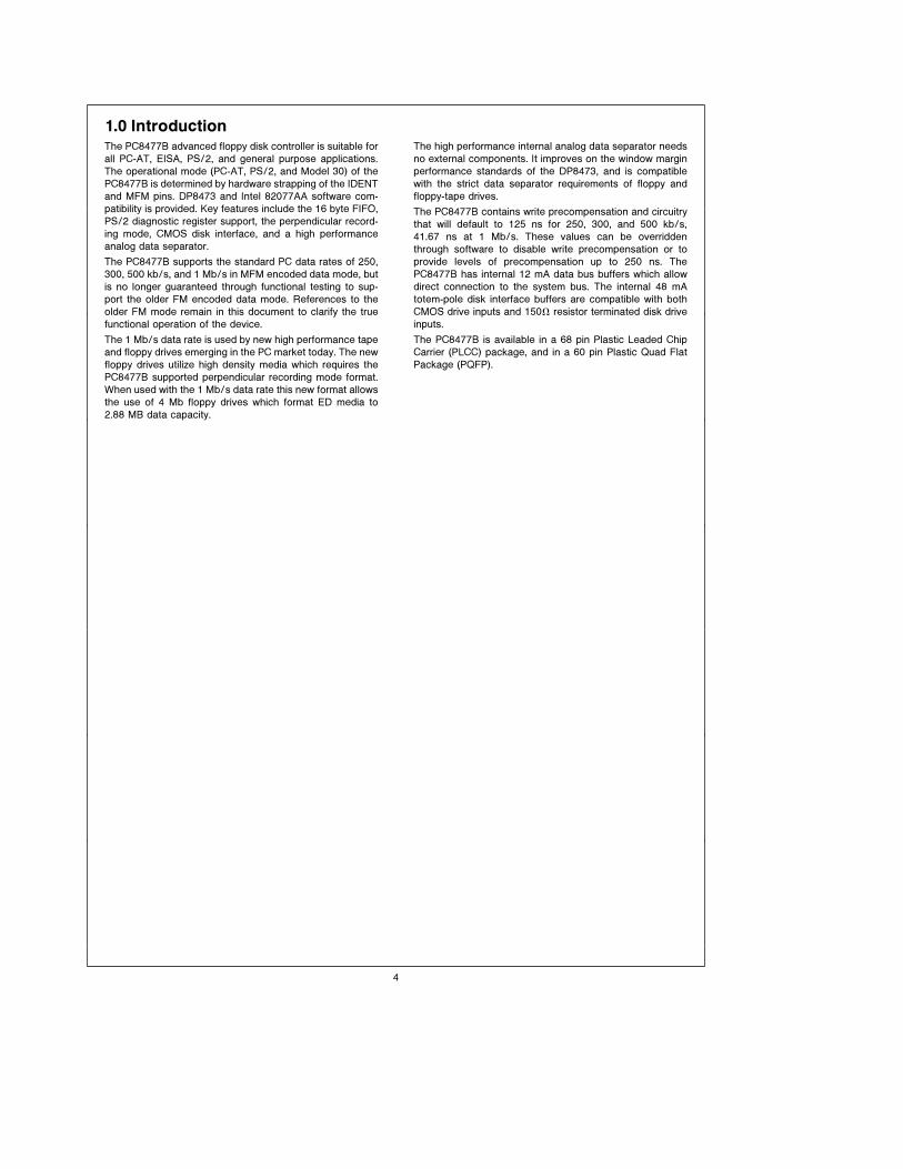
1.0 IntroductionThe PC8477B advanced floppy disk controller is suitable for
all PC-AT, EISA, PS/2, and general purpose applications.
The operational mode (PC-AT, PS/2, and Model 30) of the
PC8477B is determined by hardware strapping of the IDENT
and MFM pins. DP8473 and Intel 82077AA software com-
patibility is provided. Key features include the 16 byte FIFO,
PS/2 diagnostic register support, the perpendicular record-
ing mode, CMOS disk interface, and a high performance
analog data separator.
The PC8477B supports the standard PC data rates of 250,
300, 500 kb/s, and 1 Mb/s in MFM encoded data mode, but
is no longer guaranteed through functional testing to sup-
port the older FM encoded data mode. References to the
older FM mode remain in this document to clarify the true
functional operation of the device.
The 1 Mb/s data rate is used by new high performance tape
and floppy drives emerging in the PC market today. The new
floppy drives utilize high density media which requires the
PC8477B supported perpendicular recording mode format.
When used with the 1 Mb/s data rate this new format allows
the use of 4 Mb floppy drives which format ED media to
2.88 MB data capacity.
The high performance internal analog data separator needs
no external components. It improves on the window margin
performance standards of the DP8473, and is compatible
with the strict data separator requirements of floppy and
floppy-tape drives.
The PC8477B contains write precompensation and circuitry
that will default to 125 ns for 250, 300, and 500 kb/s,
41.67 ns at 1 Mb/s. These values can be overridden
through software to disable write precompensation or to
provide levels of precompensation up to 250 ns. The
PC8477B has internal 12 mA data bus buffers which allow
direct connection to the system bus. The internal 48 mA
totem-pole disk interface buffers are compatible with both
CMOS drive inputs and 150X resistor terminated disk drive
inputs.
The PC8477B is available in a 68 pin Plastic Leaded Chip
Carrier (PLCC) package, and in a 60 pin Plastic Quad Flat
Package (PQFP).
4
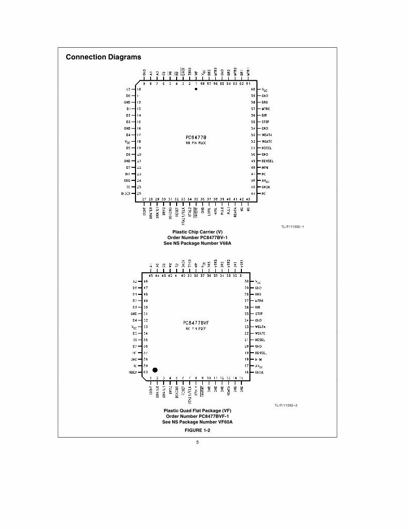
Connection Diagrams
TL/F/11332–1
Plastic Chip Carrier (V)
Order Number PC8477BV-1
See NS Package Number V68A
TL/F/11332–2
Plastic Quad Flat Package (VF)
Order Number PC8477BVF-1
See NS Package Number VF60A
FIGURE 1-2
5

2.0 Pin Description
SymbolPLCC PQFP
I/O FunctionPin Pin
A0 7 44 I Address. These address lines from the microprocessor determine which internal FDC
A1 8 45 register is accessed. See TABLE 3-1 in the Register Description section. A0–A2 are don’t
A2 10 46 cares during a DMA transfer.
AVCC 46 17 Analog Supply. This pin is the 5V supply for the analog data separator.
CS 6 43 I Chip Select. Active low input from address decoder used to enable the RD and WR inputs
during register I/O. Should be held inactive during DMA transfers.
D0 11 47 I/O Data. Bi-directional data lines to the microprocessor. D0 is the LSB and D7 is the MSB.
D1 13 48 These signals all have 12 mA buffered outputs.
D2 14 49
D3 15 50
D4 17 52
D5 19 54
D6 20 55
D7 22 56
DACK 3 40 I DMA Acknowledge. Active low input to acknowledge the DMA request and enable the RD
and WR inputs during a DMA transfer. DACK should be held inactive high during normal read
or write accesses when CS is active. When in PC-AT or Model 30 mode, this signal is
enabled by bit D3 of the DOR. When in PS/2 mode, DAK is always enabled, and bit D3 of the
DOR is reserved.
DENSEL 49 19 O Density Select. Indicates when a high density data rate (500 kb/s or 1 Mb/s) or a low
density data rate (250 or 300 kb/s) has been selected. DENSEL is active high for high
density (5.25× drives) when IDENT is high, and active low for high density (3.5× drives) when
IDENT is low. DENSEL is also programmable via the Mode command (see Section 4.2.6).
DIR 56 26 O Direction. This output determines the direction of the head movement (active e step in,
inactive e step out) during a seek operation. During read or writes, DIR will be inactive.
DR0 58 28 O Drive Select 0–3. These are the decoded drive select outputs that are controlled by Digital
DR1 62 32 Output Register bits D0, D1. The Drive Select outputs are gated by DOR bits 4–7.
DR2 64 34
DR3 67 36
DRATE0 28 2 O Data Rate 0,1. These outputs reflect the currently selected data rate, (bits 0 and 1 in the
DRATE1 29 3 CCR or the DSR, whichever was written to last). These pins are totem-pole buffered outputs
(6 mA sink, 4 mA source).
DRQ 24 58 O DMA Request. Active high output to signal the DMA controller that a data transfer is needed.
When in PC-AT or Model 30 mode, this signal is enabled by bit D3 of the DOR. When in PS/2
mode, DRQ is always enabled, and bit D3 of the DOR is reserved.
DRV2 30 4 I Drive2. This input indicates whether a second disk drive has been installed. The state of this
pin is available from Status Register A in PS/2 mode.
DSKCHG 31 5 I Disk Change. The input indicates if the drive door has been opened. The state of this pin is
available from the Digital Input register. This pin can also be configured as the RGATE data
separator diagnostic input via the Mode command (see Section 4.2.6).
GND 9, 12, 10, 11, Ground
16, 21, 12, 14,
36, 50, 15, 20,
54, 59, 24, 29,
65 51
GNDA 45 16 Analog Ground. This is the analog ground for the data separator.
6

2.0 Pin Description (Continued)
SymbolPLCC PQFP
I/O FunctionPin Pin
HDSEL 51 21 O Head Select. This output determines which side of the disk drive is accessed. Active selects side
1, inactive selects side 0.
HIFIL 38 (Note 1) High Filter. No connect. No external capacitor is required. An external capacitor can be
connected, but it will have no effect on the data separator performance.
IDENT 27 1 I Identity. During chip reset, the IDENT and MFM pins are sampled to determine the mode of
operation according to the following table:
IDENT MFM Mode
1 1 or NC PC-AT Mode
1 0 Illegal
0 1 or NC PS/2 Mode
0 0 Model 30 Mode
AT ModeÐThe DMA enable bit in the DOR is valid. TC is active high. Status Registers A and B
are disabled (TRI-STATEÉ).
Model 30 ModeÐThe DMA enable bit in the DOR is valid. TC is active high. Status Registers A
and B are enabled.
PS/2 ModeÐThe DMA enable bit in the DOR is a don’t care, and the DRQ and INT signals will
always be enabled. TC is active low. Status Registers A and B are enabled.
After chip reset, the state of IDENT determines the polarity of the DENSEL output.
When IDENT is a logic ‘‘1’’, DENSEL is active high for 500 kb/s and 1 Mb/s data rates.
When IDENT is a logic ‘‘0’’, DENSEL is active low for 500 kb/s and 1 Mb/s data rates.
(See Mode command for further explanation of DENSEL.)
INDEX 26 60 I Index. This input signals the beginning of a track.
INT 23 57 O Interrupt. Active high output to signal the completion of the execution phase for certain
commands. Also used to signal when a data transfer is ready during a Non-DMA operation. When
in PC-AT or Model 30 mode, this signal is enabled by bit D3 of the DOR. When in PS/2 mode, INT
is always enabled, and bit D3 of the DOR is reserved.
INVERT 35 9 I Invert. Determines the polarity of all disk interface signals. When tied low, the internal disk output
buffers and inverting Schmitt input receivers are enabled, and the disk interface signals are active
low. When tied high, the disk interface signals are active high, and external receivers and output
buffers are required.
LOFIL 37 (Note 1) Low Filter. No connect. No external capacitor is required. An external capacitor can be
connected, but it will have no effect on the data separator performance.
MFM 48 18 I/O MFM. During a chip reset when in PS/2 mode (IDENT low), this pin is sampled to select the PS/2
mode (MFM high), or the Model 30 mode (MFM low). An internal pull-up or external pull-down
10 kX resistor will select between the two PS/2 modes. When the PC-AT mode is desired (IDENT
high), MFM should be left pulled high internally. MFM reflects the current data encoding format
when RESET is inactive. MFM e high, FM e low. Defaults to low after a chip reset. This signal
can also be configured as the PUMP data separator diagnostic output via the Mode command (see
Section 4.2.6).
MTR0 57 27 O Motor Select 0–3. These are the motor enable lines for drives 0–3, and are controlled by bits D7–
D4 of the Digital Output register.MTR1 61 31
MTR2 63 33
MTR3 66 35
NC 42 (Note 1) No Connect. These pins must be left unconnected.
43
44
47
7

2.0 Pin Description (Continued)
SymbolPLCC PQFP
I/O FunctionPin Pin
PLL0 39 (Note 1) Phase Locked Loop 0,1. No connects. These pins can be tied high or low with no affect
PLL1 40 on the data separator performance.
RD 4 41 I Read. Active low input to signal a read from the controller to the microprocessor.
RDATA 41 13 I Read Data. This input is the raw serial data read from the disk drive.
RESET 32 6 I Reset. Active high input that resets the controller to the idle state, and resets all disk
interface outputs to their inactive states. The DOR, DSR, CCR, Mode command,
Configure command, and Lock command parameters are cleared to their default values.
The Specify command parameters are not affected.
STEP 55 25 O Step. This output signal issues pulses to the disk drive at a software programmable rate
to move the head during a seek operation.
TC 25 59 I Terminal Count. Control signal from the DMA controller to indicate the termination of a
DMA transfer. TC is accepted only when DACK is active. TC is active high in PC-AT and
Model 30 modes, and active low in PS/2 mode.
TRK0 2 39 I Track 0. This input indicates to the controller that the head of the selected disk drive is at
track zero.
VCC 18 30 Voltage. This is the a5V supply voltage for the digital circuitry.
60 37
68 53
WDATA 53 23 O Write Data. This output is the write precompensated serial data that is written to the
selected disk drive. Precompensation is software selectable.
WGATE 52 22 O Write Gate. This output signal enables the write circuitry of the selected disk drive.
WGATE has been designed to prevent glitches during power up and power down. This
prevents writing to the disk when power is cycled.
WP 1 38 I Write Protect. This input indicates that the disk in the selected drive is write protected.
WR 5 42 I Write. Active low input to signal a write from the microprocessor to the controller.
XTAL1/CLK 33 7 I Crystal1/Clock. One side of an external 24 MHz crystal is attached here. If a crystal is
not used, a TTL or CMOS compatible clock is connected to this pin.
XTAL2 34 8 I Crystal2. One side of an external 24 MHz crystal is attached here. This pin is left
unconnected if an external clock is used.
Note 1: When converting the 68 pin PLCC to a 60 pin PQFP, eight pins were removed. The following signals were affected in this conversion process:
1. NC (No Connect) signals on pins 42 and 43 of the 68 pin PLCC were converted to GND (Ground) signals on pins 14 and 15 of the 60 pin PQFP,
respectively.
2. NC (No Connect) signals on pins 44 and 47 of the 68 pin PLCC were removed for the 60 pin PQFP.
3. HIFIL (pin 38) and LOFIL (pin 37) of the 68 pin PLCC were removed for the 60 pin PQFP.
4. PLL0 (pin 39) and PLL1 (pin 40) of the 68 PLCC were converted to GND (ground) signals on the PQFP (pins 11 and 12 respectively).
5. The GND (ground) signals on pins 9, 12, 21, and 65 of the 68 pin PLCC are not available for the 60 pin PQFP. These signals are tied to ground internally.
8
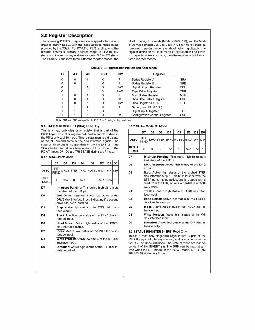
3.0 Register DescriptionThe following PC8477B registers are mapped into the ad-
dresses shown below, with the base address range being
provided by the CS pin. For PC-AT or PS/2 applications, the
diskette controller primary address range is 3F0 to 3F7
(hex), and the secondary address range is 370 to 377 (hex).
The PC8477B supports three different register modes: the
PC-AT mode, PS/2 mode (Models 50/60/80), and the Mod-
el 30 mode (Model 30). See Section 5.1 for more details on
how each register mode is enabled. When applicable, the
register definition for each mode of operation will be given.
If no special notes are made, then the register is valid for all
three register modes.
TABLE 3-1. Register Description and Addresses
A2 A1 A0 IDENT R/W Register
0 0 0 0 R Status Register A SRA
0 0 1 0 R Status Register B SRB
0 1 0 X R/W Digital Output Register DOR
0 1 1 X R/W Tape Drive Register TDR
1 0 0 X R Main Status Register MSR
1 0 0 X W Data Rate Select Register DSR
1 0 1 X R/W Data Register (FIFO) FIFO
1 1 0 X X None (Bus TRI-STATE)
1 1 1 X R Digital Input Register DIR
1 1 1 X W Configuration Control Register CCR
Note: SRA and SRB are enabled by IDENT e 0 during a chip reset only.
3.1 STATUS REGISTER A (SRA) Read Only
This is a read only diagnostic register that is part of the
PS/2 floppy controller register set, and is enabled when in
the PS/2 or Model 30 mode. This register monitors the state
of the INT pin and some of the disk interface signals. The
state of these bits is independent of the INVERT pin. The
SRA can be read at any time when in PS/2 mode. In the
PC-AT mode, D7–D0 are TRI-STATE during a mP read.
3.1.1 SRAÐPS/2 Mode
D7 D6 D5 D4 D3 D2 D1 D0
DESCINT
DRV2 STEP TRK0 HDSEL INDX WP DIRPEND
RESET0 N/A 0 N/A 0 N/A N/A 0
COND
D7 Interrupt Pending: This active high bit reflects
the state of the INT pin.
D6 2nd Drive Installed: Active low status of the
DRV2 disk interface input, indicating if a second
drive has been installed.
D5 Step: Active high status of the STEP disk inter-
face output.
D4 Track 0: Active low status of the TRK0 disk in-
terface input.
D3 Head Select: Active high status of the HDSEL
disk interface output.
D2 Index: Active low status of the INDEX disk in-
terface input.
D1 Write Protect: Active low status of the WP disk
interface input.
D0 Direction: Active high status of the DIR disk in-
terface output.
3.1.2 SRAÐ Model 30 Mode
D7 D6 D5 D4 D3 D2 D1 D0
DESCINT
DRQ STEP TRK0 HDSEL INDX WP DIRPEND
RESET0 0 0 N/A 1 N/A N/A 1
COND
D7 Interrupt Pending: This active high bit reflects
that state of the INT pin.
D6 DMA Request: Active high status of the DRQ
signal.
D5 Step: Active high status of the latched STEP
disk interface output. This bit is latched with the
STEP output going active, and is cleared with a
read from the DIR, or with a hardware or soft-
ware reset.
D4 Track 0: Active high status of TRK0 disk inter-
face input.
D3 Head Select: Active low status of the HDSEL
disk interface output.
D2 Index: Active high status of the INDEX disk in-
terface input.
D1 Write Protect: Active high status of the WP
disk interface input.
D0 Direction: Active low status of the DIR disk in-
terface output.
3.2 STATUS REGISTER B (SRB) Read Only
This is a read only diagnostic register that is part of the
PS/2 floppy controller register set, and is enabled when in
the PS/2 or Model 30 mode. The state of these bits is inde-
pendent of the INVERT pin. The SRB can be read at any
time when in PS/2 mode. In the PC-AT mode, D7–D0 are
TRI-STATE during a mP read.
9

3.0 Register Description (Continued)
3.2.1 SRBÐPS/2 Mode
D7 D6 D5 D4 D3 D2 D1 D0
DESC 1 1 DR0 WDATA RDATA WGATE MTR1 MTR0
RESETN/A N/A 0 0 0 0 0 0
COND
D7 Reserved: Always 1.
D6 Reserved: Always 1.
D5 Drive Select 0: Reflects the status of the Drive
Select 0 bit in the DOR (address 2, bit 0). This
bit is cleared after a hardware reset, not a soft-
ware reset.
D4 Write Data: Every inactive edge transition of
the WDATA disk interface output causes this bit
to change states.
D3 Read Data: Every positive edge transition of the
RDATA disk interface output causes this bit to
change states.
D2 Write Gate: Active high status of the WGATE
disk interface output.
D1 Motor Enable 1: Active high status of the
MTR1 disk interface output. Low after a hard-
ware reset, unaffected by a software reset.
D0 Motor Enable 0: Active high status of the
MTR0 disk interface output. Low after a hard-
ware reset, unaffected by a software reset.
3.2.2 SRBÐModel 30 Mode
D7 D6 D5 D4 D3 D2 D1 D0
DESC DRV2 DR1 DR0 WDATA RDATA WGATE DR3 DR2
RESETN/A 1 1 0 0 0 1 1
COND
D7 2nd Drive Installed: Active low status of the
DRV2 disk interface input.
D6 Drive Select 1: Active low status of the DR1
disk interface output.
D5 Drive Select 0: Active low status of the DR0
disk interface output.
D4 Write Data: Active high status of latched
WDATA signal. This bit is latched by the inac-
tive going edge of WDATA and is cleared by a
read from the DIR. This bit is not gated by
WGATE.
D3 Read Data: Active high status of latched
RDATA signal. This bit is latched by the inactive
going edge of RDATA and is cleared by a read
from the DIR.
D2 Write Gate: Active high status of latched
WGATE signal. This bit is latched by the active
going edge of WGATE and is cleared by a read
from the DIR.
D1 Drive Select 3: Active low status of the DR3
disk interface output.
D0 Drive Select 2: Active low status of the DR2
disk interface output.
3.3 DIGITAL OUTPUT REGISTER (DOR) Read/Write
The DOR controls the drive select and motor enable disk
interface outputs, enables the DMA logic, and contains a
software reset bit. The contents of the DOR are set to 00
(hex) after a hardware reset, and are unaffected by a soft-
ware reset. The DOR can be written to at any time.
DOR
D7 D6 D5 D4 D3 D2 D1 D0
DESC MTR3 MTR2 MTR1 MTR0 DMAEN RESETDRIVE DRIVE
SEL 1 SEL 0
RESET0 0 0 0 0 0 0 0
COND
D7 Motor Enable 3: This bit controls the MTR3
disk interface output. A 1 in this bit causes the
MTR3 pin to go active. The actual level of
MTR3 depends on the state of the INVERT pin.
D6 Motor Enable 2: Same function as D7 except
for MTR2.
D5 Motor Enable 1: Same function as D7 except
for MTR1.
D4 Motor Enable 0: Same function as D7 except
for MTR0.
D3 DMA Enable: This bit has two modes of opera-
tion. PC-AT mode or Model 30 mode: Writing
a 1 to this bit will enable the DRQ, DAK, INT
and TC pins. Writing a 0 to this bit will
TRI-STATE DRQ and INT, and disable DAK and
TC. This bit is a 0 after a reset when in these
modes. PS/2 mode: This bit is reserved, and
the DRQ, DAK, INT and TC pins will always be
enabled. During a reset, the DRQ, DAK, and
INT lines will remain enabled, and D3 will be a
0.
D2 Reset Controller: Writing a 0 to this bit resets
the controller. It will remain in the reset condi-
tion until a 1 is written to this bit. A software
reset does not affect the DSR, CCR, and other
bits of the DOR. A software reset will affect the
Configure and Mode command bits (see Sec-
tion 4.0 Command Set Description). The mini-
mum time that this bit must be low is 100 ns.
Thus, toggling the Reset Controller bit during
consecutive writes to the DOR is an acceptable
method of issuing a software reset.
D1–D0 Drive Select: These two bits are binary encod-
ed for the four drive selects DR0–DR3, so that
only one drive select output is active at a time.
The actual level of the drive select outputs is
determined by the state of the INVERT pin.
It is common programming practice to enable both the mo-
tor enable and drive select outputs for a particular drive.
Table 3-2 below shows the DOR values to enable each of
the four drives.
TABLE 3-2. Drive Enable Values
Drive DOR Value
0 1C (Hex)
1 2D
2 4E
3 8F
10

3.0 Register Description (Continued)
3.4 DRIVE REGISTER (TDR) Read/Write
This register is used to assign a particular drive number with
the tape drive support mode of the data separator. All other
logical drives are assigned floppy drive support with the
data separator. Any future reference to the assigned tape
drive will invoke tape drive support. The TDR is unaffected
by a software reset.
TDR
D7 D6 D5 D4 D3 D2 D1 D0
DESC X X X X X XTAPE TAPE
SEL1 SEL0
RESETN/A N/A N/A N/A N/A N/A 0 0
COND
D7–D2 Reserved: These bits are ignored when written
to and are TRI-STATE when read.
D1–D0 Tape Select 1,0: These two bits assign a logical
drive number to be a tape drive. Drive 0 is not
available as a tape drive, and is reserved as the
floppy disk boot drive. See Table 3-3 for the
tape drive assignment values.
TABLE 3-3. Tape Drive Assignment Values
TAPESEL1 TAPESEL0DRIVE
SELECTED
0 0 None
0 1 1
1 0 2
1 1 3
3.5 MAIN STATUS REGISTER (MSR) Read Only
The read only Main Status Register indicates the current
status of the disk controller. The Main Status Register is
always available to be read. One of its functions is to control
the flow of data to and from the Data Register (FIFO). The
Main Status Register indicates when the disk controller is
ready to send or receive data through the Data Register. It
should be read before each byte is transferred to or from
the Data Register except during a DMA transfer. No delay is
required when reading this register after a data transfer.
After a hardware or software reset, or recovery from a pow-
er down state, the Main Status Register is immediately avail-
able to be read by the mP. It will contain a value of 00 hex
until the oscillator circuit has stabilized, and the internal reg-
isters have been initialized. When the PC8477B is ready to
receive a new command, it will report an 80 hex to the mP.
The system software can poll the MSR until it is ready. The
worst case time allowed for the MSR to report an 80 hex
value (RQM set) is 2.5 ms after reset or power up.
MSR
D7 D6 D5 D4 D3 D2 D1 D0
DESCRQM DIO NON CMD DRV3 DRV2 DRV1 DRV0
DMA PROG BUSY BUSY BUSY BUSY
RESET0 0 0 0 0 0 0 0
COND
D7 Request for Master: Indicates that the control-
ler is ready to send or receive data from the mP
through the FIFO. This bit is cleared immediate-
ly after a byte transfer and will become set
again as soon as the disk controller is ready for
the next byte. During a Non-DMA Execution
phase, the RQM indicates the status of the in-
terrupt pin.
D6 Data I/O (Direction): Indicates whether the
controller is expecting a byte to be written to (0)
or read from (1) the Data Register.
D5 Non-DMA Execution: Indicates that the con-
troller is in the Execution Phase of a byte trans-
fer operation in the Non-DMA mode. Used for
multiple byte transfers by the mP in the Execu-
tion Phase through interrupts or software poll-
ing.
D4 Command in Progress: This bit is set after the
first byte of the Command Phase is written. This
bit is cleared after the last byte of the Result
Phase is read. If there is no Result Phase in a
command, the bit is cleared after the last byte
of the Command Phase is written.
D3 Drive 3 Busy: Set after the last byte of the
Command Phase of a Seek or Recalibrate com-
mand is issued for drive 3. Cleared after reading
the first byte in the Result Phase of the Sense
Interrupt Command for this drive.
D2 Drive 2 Busy: Same as above for drive 2.
D1 Drive 1 Busy: Same as above for drive 1.
D0 Drive 0 Busy: Same as above for drive 0.
3.6 DATA RATE SELECT REGISTER (DSR) Write Only
This write only register is used to program the data rate,
amount of write precompensation, power down mode, and
software reset. The data rate is programmed via the CCR,
not the DSR, for PC-AT and PS/2 Model 30 and MicroChan-
nel applications. Other applications can set the data rate in
the DSR. The data rate of the floppy controller is deter-
mined by the most recent write to either the DSR or CCR.
The DSR is unaffected by a software reset. A hardware re-
set will set the DSR to 02 (hex), which corresponds to the
default precompensation setting and 250 kb/s.
DSR
D7 D6 D5 D4 D3 D2 D1 D0
DESCS/W LOW
0PRE- PRE- PRE-
DRATE1 DRATE0RESET PWR COMP2 COMP1 COMP0
RESET0 0 0 0 0 0 1 0
COND
D7 Software Reset: A 1 in this bit location will re-
set the part similar to the DOR RESET (D2) ex-
cept that this software reset is self-clearing.
D6 Low Power: A 1 to this bit will put the controller
into the Manual Low Power mode. The oscilla-
tor and data separator circuits will be turned off.
Manual Low Power can also be accessed via
the Mode command. The chip will come out of
low power after a software reset, or access to
the Data Register or Main Status Register.
11
3.0 Register Description (Continued)
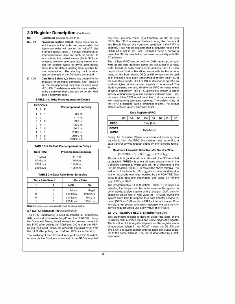
D5 Undefined: Should be set to 0.
D4–D2 Precompensation Select: These three bits se-
lect the amount of write precompensation the
floppy controller will use on the WDATA disk
interface output. Table 3-4 shows the amount of
precompensation used for each bit pattern. In
most cases, the default values (Table 3-5) can
be used; however, alternate values can be cho-
sen for specific types of drives and media.
Track 0 is the default starting track number for
precompensation. The starting track number
can be changed in the Configure command.
D1–D0 Data Rate Select 1,0: These bits determine the
data rate for the floppy controller. See Table 3-6
for the corresponding data rate for each value
of D1, D0. The data rate select bits are unaffect-
ed by a software reset, and are set to 250 kb/s
after a hardware reset.
TABLE 3-4. Write Precompensation Delays
PRECOMPPrecompensation Delay
4 3 2
1 1 1 0.0 ns
0 0 1 41.7 ns
0 1 0 83.3 ns
0 1 1 125.0 ns
1 0 0 166.7 ns
1 0 1 208.3 ns
1 1 0 250.0 ns
0 0 0 DEFAULT
TABLE 3-5. Default Precompensation Delays
Data Rate Precompensation Delay
1 Mb/s 41.7 ns
500 kb/s 125.0 ns
300 kb/s 125.0 ns
250 kb/s 125.0 ns
TABLE 3-6. Data Rate Select Encoding
Data Rate Select Data Rate
1 2 MFM FM
1 1 1 Mb/s Illegal
0 0 500 kb/s 250 kb/s
0 1 300 kb/s 150 kb/s
1 0 250 kb/s 125 kb/s
Note: FM mode is not guaranteed through functional testing.
3.7 DATA REGISTER (FIFO) Read/Write
The FIFO (read/write) is used to transfer all commands,
data, and status between the mP and the PC8477B. During
the Command Phase, the mP writes the command bytes into
the FIFO after polling the RQM and DIO bits in the MSR.
During the Result Phase, the mP reads the result bytes from
the FIFO after polling the RQM and DIO bits in the MSR.
The enabling of the FIFO and setting of the FIFO threshold
is done via the Configure command. If the FIFO is enabled,
only the Execution Phase byte transfers use the 16 byte
FIFO. The FIFO is always disabled during the Command
and Result Phases of a controller operation. If the FIFO is
enabled, it will not be disabled after a software reset if the
LOCK bit is set in the Lock Command. After a hardware
reset, the FIFO is disabled to maintain compatibility with PC-
AT systems.
The 16 byte FIFO can be used for DMA, Interrupt, or soft-
ware polling type transfers during the execution of a read,
write, format, or scan command. In addition, the FIFO can
be put into a Burst or Non-Burst mode with the Mode com-
mand. In the Burst mode, DRQ or INT remains active until
all of the bytes have been transferred to or from the FIFO. In
the Non-Burst mode, DRQ or INT is deasserted for 350 ns
to allow higher priority transfer requests to be serviced. The
Mode command can also disable the FIFO for either reads
or writes separately. The FIFO allows the system a larger
latency without causing a disk overrun/underrun error. Typi-
cal uses of the FIFO would be at the 1 Mb/s data rate, or
with multi-tasking operating systems. The default state of
the FIFO is disabled, with a threshold of zero. The default
state is entered after a hardware reset.
Data Register (FIFO)
D7 D6 D5 D4 D3 D2 D1 D0
DESC Data [7:0]
RESETByte Mode
COND
During the Execution Phase of a command involving data
transfer to/from the FIFO, the system must respond to a
data transfer service request based on the following formu-
la:
Maximum Allowable Data Transfer Service Time
(THRESH a 1) c 8 c tDRP b (16 c tICP)
This formula is good for all data rates with the FIFO enabled
or disabled. THRESH is a four bit value programmed in the
Configure command, which sets the FIFO threshold. If the
FIFO is disabled, THRESH is zero in the above formula. The
last term of the formula, (16 c tICP) is an inherent delay due
to the microcode overhead required by the PC8477B. This
delay is also data rate dependent. See Table 6-1 for the
tDRP and tICP times.
The programmable FIFO threshold (THRESH) is useful in
adjusting the floppy controller to the speed of the system. In
other words, a slow system with a sluggish DMA transfer
capability would use a high value of THRESH, giving the
system more time to respond to a data transfer service re-
quest (DRQ for DMA mode or INT for Interrupt mode). Con-
versely, a fast system with quick response to a data transfer
service request would use a low value of THRESH.
3.8 DIGITAL INPUT REGISTER (DIR) Read Only
This diagnostic register is used to detect the state of the
DSKCHG disk interface input and some diagnostic signals.
The function of this register depends on the register mode
of operation. When in the PC-AT mode, the D6–D0 are
TRI-STATE to avoid conflict with the fixed disk status regis-
ter at the same address. The DIR is unaffected by a soft-
ware reset.
12

3.0 Register Description (Continued)
3.8.1 DIRÐPC-AT Mode
D7 D6 D5 D4 D3 D2 D1 D0
DESC DSKCHG X X X X X X X
RESETN/A N/A N/A N/A N/A N/A N/A N/A
COND
D7 Disk Changed: Active high status of DSKCHG
disk interface input, independent of INVERT
value.
D6–D0 Undefined: TRI-STATE. Used by hard disk con-
troller status register.
3.8.2 DIRÐPS/2 Mode
D7 D6 D5 D4 D3 D2 D1 D0
DESC DSKCHG 1 1 1 1 DRATE1 DRATE0HIGH
DEN
RESETN/A N/A N/A N/A N/A N/A N/A 1
COND
D7 Disk Changed: Active high status of DSKCHG
disk interface input, independent of INVERT
value.
D6–D3 Reserved: Always 1.
D2–D1 Data Rate Select 1,0: These bits indicate the
status of the DRATE1–0 bits programmed
through the DSR/CCR.
D0 High Density: This bit is low when the 1 Mb/s
or 500 kb/s data rate is chosen, and high when
the 300 kb/s or 250 kb/s data rate is chosen.
This bit is independent of the IDENT or INVERT
value.
3.8.3 DIRÐModel 30 Mode
D7 D6 D5 D4 D3 D2 D1 D0
DESC DSKCHG 0 0 0 DMAEN NOPRE DRATE1 DRATE0
RESETN/A 0 0 0 0 0 1 0
COND
D7 Disk Changed: Active low status of DSKCHG
disk interface input, independent of INVERT
value.
D6–D4 Reserved: Always 0.
D3 DMA Enable: Active high status of the DMAEN
bit in the DOR.
D2 No Precompensation: Active high status of the
NOPRE bit in the CCR.
D1–D0 Data Rate Select 1,0: These bits indicate the
status of the DRATE1–0 bits programmed
through the DSR/CCR.
3.9 CONFIGURATION CONTROL REGISTER (CCR) Write
Only
This is the write only data rate register commonly used in
PC-AT applications. This register is not affected by a soft-
ware reset, and is set to 250 kb/s after a hardware reset.
The data rate of the floppy controller is determined by the
last write to either the CCR or DSR.
3.9.1 CCRÐPC-AT and PS/2 Modes
D7 D6 D5 D4 D3 D2 D1 D0
DESC 0 0 0 0 0 0 DRATE1 DRATE0
RESETN/A N/A N/A N/A N/A N/A 1 0
COND
D7–D2 Reserved: Should be set to 0.
D1–D0 Data Rate Select 1,0: These bits determine the
data rate of the floppy controller. See Table 3-6
for the appropriate values.
3.9.2 CCRÐModel 30 Mode
D7 D6 D5 D4 D3 D2 D1 D0
DESC 0 0 0 0 0 NOPRE DRATE1 DRATE0
RESETN/A N/A N/A N/A N/A 0 1 0
COND
D7–D3 Reserved: Should be set to 0.
D2 No Precompensation: This bit can be set by
software, but it has no functionality. It can be
read by bit D2 of the DIR when in the Model 30
register mode. Unaffected by a software reset.
D1–D0 Data Rate Select 1,0: These bits determine the
data rate of the floppy controller. See Table 3-6
for the appropriate values.
3.10 RESULT PHASE STATUS REGISTERS
The Result Phase of a command contains bytes that hold
status information. The format of these bytes are described
below. Do not confuse these status bytes with the Main
Status Register, which is a read only register that is always
valid. The Result Phase status registers are read from the
Data Register (FIFO) only during the Result Phase of certain
commands (see Section 4.1 Command Set Summary). The
status of each register bit is indicated when the bit is a 1.
3.10.1 Status Register 0 (ST0)
D7 D6 D5 D4 D3 D2 D1 D0
DESC IC IC SE EC 0 HDS DS1 DS0
RESET0 0 0 0 0 0 0 0
COND
D7–D6 Interrupt Code:
00 e Normal Termination of Command.
01 e Abnormal Termination of Command. Exe-
cution of command was started, but was
not successfully completed.
10 e Invalid Command Issued. Command is-
sued was not recognized as a valid com-
mand.
11 e Internal drive ready status changed state
during the drive polling mode. Only occurs
after a hardware or software reset.
D5 Seek End: Seek, Relative Seek, or Recalibrate
command completed by the controller. (Used
during a Sense Interrupt command.)
D4 Equipment Check: After a Recalibrate com-
mand, Track 0 signal failed to occur. (Used dur-
ing Sense Interrupt command.)
D3 Not Used. Always 0.
13

3.0 Register Description (Continued)
D2 Head Select: Indicates the active high status of
the HDSEL pin at the end of the Execution
Phase.
D1–D0 Drive Select 1,0: These two binary encoded
bits indicate the logical drive selected at the end
of the Execution Phase.
00 e Drive 0 selected.
01 e Drive 1 selected.
10 e Drive 2 selected.
11 e Drive 3 selected.
3.10.2 Status Register 1 (ST1)
D7 D6 D5 D4 D3 D2 D1 D0
DESC ET 0 CE OR 0 ND NW MA
RESET0 0 0 0 0 0 0 0
COND
D7 End of Track: Controller transferred the last
byte of the last sector without the TC pin be-
coming active. The last sector is the End of
Track sector number programmed in the Com-
mand Phase.
D6 Not Used. Always 0.
D5 CRC Error: If this bit is set and bit 5 of ST2 is
clear, then there was a CRC error in the Ad-
dress Field of the correct sector. If bit 5 of ST2
is also set, then there was a CRC error in the
Data Field.
D4 Overrun: Controller was not serviced by the mP
soon enough during a data transfer in the Exe-
cution Phase. For read operations, indicates a
data overrun. For write operations, indicates a
data underrun.
D3 Not Used. Always 0.
D2 No Data: Three possible problems:
1. Controller cannot find the sector specified in
the Command Phase during the execution of
a Read, Write, Scan, or Verify command. An
address mark was found however, so it is not
a blank disk.
2. Controller cannot read any Address Fields
without a CRC error during a Read ID com-
mand.
3. Controller cannot find starting sector during
execution of Read A Track command.
D1 Not Writable: Write Protect pin is active when a
Write or Format command is issued.
D0 Missing Address Mark: If bit 0 of ST2 is clear
then the controller cannot detect any Address
Field Address Mark after two disk revolutions. If
bit 0 of ST2 is set then the controller cannot
detect the Data Field Address Mark after finding
the correct Address Field.
3.10.3 Status Register 2 (ST2)
D7 D6 D5 D4 D3 D2 D1 D0
DESC 0 CM CD WT SEH SNS BT MD
RESET0 0 0 0 0 0 0 0
COND
D7 Not Used. Always 0.
D6 Control Mark: Controller tried to read a sector
which contained a deleted data address mark
during execution of Read Data or Scan com-
mands. Or, if a Read Deleted Data command
was executed, a regular address mark was de-
tected.
D5 CRC Error in Data Field: Controller detected a
CRC error in the Data Field. Bit 5 of ST1 is also
set.
D4 Wrong Track: Only set if desired sector is not
found, and the track number recorded on any
sector of the current track is different from the
track address specified in the Command Phase.
D3 Scan Equal Hit: ‘‘Equal’’ condition satisfied dur-
ing any Scan command.
D2 Scan Not Satisfied: Controller cannot find a
sector on the track which meets the desired
condition during any Scan command.
D1 Bad Track: Only set if the desired sector is not
found, the track number recorded on any sector
on the track is FF (hex) indicating a hard error in
IBM format, and is different from the track ad-
dress specified in the Command Phase.
D0 Missing Address Mark in Data Field: Control-
ler cannot find the Data Field AM during a Read,
Scan, or Verify command. Bit 0 of ST1 is also
set.
3.10.4 Status Register 3 (ST3)
D7 D6 D5 D4 D3 D2 D1 D0
DESC 0 WP 1 TK0 1 HDS DS1 DS0
RESET0 0 1 0 1 0 0 0
COND
D7 Not Used. Always 0.
D6 Write Protect: Indicates active high status of
the WP pin.
D5 Not Used. Always 1.
D4 Track 0: Indicates active high status of the
TRK0 pin.
D3 Not Used. Always 1.
D2 Head Select: Indicates the active high status of
the HD bit in the Command Phase.
D1–D0 Drive Select 1,0: These two binary encoded
bits indicate the DS1–DS0 bits in the Command
Phase.
14
4.0 Command Set DescriptionThe following is a table of the PC8477B command set. Each
command contains a unique first command byte called the
opcode byte which will identify to the controller how many
command bytes to expect. If an invalid command byte is
issued to the controller, it will immediately go into the Result
Phase and the status will be 80 (hex), which signifies Invalid
Command.
4.1 COMMAND SET SUMMARY
CONFIGURE
Command Phase
0 0 0 1 0 0 1 1
0 0 0 0 0 0 0 0
0 EIS FIFO POLL THRESH
PRETRK
Execution Phase: Internal registers written.
No Result Phase
DUMPREG
Command Phase
0 0 0 0 1 1 1 0
Execution Phase: Internal registers read.
Result Phase
PTR Drive 0
PTR Drive 1
PTR Drive 2
PTR Drive 3
Step Rate Time Motor Off Time
Motor On Time DMA
Sectors per Track/End of Track
LOCK 0 DC3 DC2 DC1 DC0 GAP WG
0 EIS FIFO POLL THRESH
PRETRK
Note: Sectors per Track parameter returned if last command issued was
Format. End of Track parameter returned if last command issued was Read
or Write.
FORMAT TRACK
Command Phase
0 MFM 0 0 1 1 0 1
X X X X X HD DR1 DR0
Bytes per Sector
Sectors per Track
Format Gap
Data Pattern
Execution Phase: System transfers four ID bytes (track,
head, sector, bytes/sector) per sector to the floppy control-
ler via DMA or Non-DMA modes. The entire track is format-
ted. The data block in the Data Field of each sector is filled
with the data pattern byte.
Result Phase
Status Register 0
Status Register 1
Status Register 2
Undefined
Undefined
Undefined
Undefined
INVALID
Command Phase
Invalid Op Codes
Result Phase
Status Register 0 (80 hex)
LOCK
Command Phase
LOCK 0 0 1 0 1 0 0
Execution Phase: Internal register is written.
Result Phase
0 0 0 LOCK 0 0 0 0
MODE
Command Phase
0 0 0 0 0 0 0 1
TMR IAF IPS 0 LOW PWR 1 ETR
FWR FRD BST R255 0 0 0 0
DENSEL BFR WLD Head Settle
0 0 0 0 0 RG O PU
Execution Phase: Internal registers are written.
No Result Phase
NSC
Command Phase
0 0 0 1 1 0 0 0
Result Phase
0 1 1 1 0 0 1 1
PERPENDICULAR MODE
Command Phase
0 0 0 1 0 0 1 0
OW 0 DC3 DC2 DC1 DC0 GAP WG
Execution Phase: Internal registers are written.
No Result Phase
15

4.0 Command Set Description (Continued)
READ DATA
Command Phase
MT MFM SK 0 0 1 1 0
IPS X X X X HD DR1 DR0
Track Number
Drive Head Number
Sector Number
Bytes per Sector
End of Track Sector Number
Intersector Gap Length
Data Length
Execution Phase: Data read from disk drive is transferred
to system via DMA or Non-DMA modes.
Result Phase
Status Register 0
Status Register 1
Status Register 2
Track Number
Head Number
Sector Number
Bytes per Sector
READ DELETED DATA
Command Phase
MT MFM SK 0 1 1 0 0
IPS X X X X HD DR1 DR0
Track Number
Drive Head Number
Sector Number
Bytes per Sector
End of Track Sector Number
Intersector Gap Length
Data Length
Execution Phase: Data read from disk drive is transferred
to system via DMA or Non-DMA modes.
Result Phase
Status Register 0
Status Register 1
Status Register 2
Track Number
Head Number
Sector Number
Bytes per Sector
READ ID
Command Phase
0 MFM 0 0 1 0 1 0
X X X X X HD DR1 DR0
Execution Phase: Controller reads first ID Field header
bytes it can find and reports these bytes to the system in the
result bytes.
Result Phase
Status Register 0
Status Register 1
Status Register 2
Track Number
Head Number
Sector Number
Bytes per Sector
READ A TRACK
Command Phase
0 MFM 0 0 0 0 1 0
IPS X X X X HD DR1 DR0
Track Number
Drive Head Number
Sector Number
Bytes per Sector
End of Track Sector Number
Intersector Gap Length
Data Length
Execution Phase: Data read from disk drive is transferred
to system via DMA or Non-DMA modes.
Result Phase
Status Register 0
Status Register 1
Status Register 2
Track Number
Head Number
Sector Number
Bytes per Sector
RECALIBRATE
Command Phase
0 0 0 0 0 1 1 1
0 0 0 0 0 0 DR1 DR0
Execution Phase: Disk drive head is stepped out to
Track 0.
No Result Phase
RELATIVE SEEK
Command Phase
1 DIR 0 0 1 1 1 1
X X X X X HD DR1 DR0
Relative Track Number
Execution Phase: Disk drive head stepped in or out a
programmable number of tracks.
No Result Phase
16

4.0 Command Set Description (Continued)
SCAN EQUAL
Command Phase
MT MFM SK 1 0 0 0 1
IPS X X X X HD DR1 DR0
Track Number
Drive Head Number
Sector Number
Bytes per Sector
End of Track Sector Number
Intersector Gap Length
Sector Step Size
Execution Phase: Data transferred from system to
controller is compared to data read from disk.
Result Phase
Status Register 0
Status Register 1
Status Register 2
Track Number
Head Number
Sector Number
Bytes per Sector
SCAN HIGH OR EQUAL
Command Phase
MT MFM SK 1 1 1 0 1
IPS X X X X HD DR1 DR0
Track Number
Drive Head Number
Sector Number
Bytes per Sector
End of Track Sector Number
Intersector Gap Length
Sector Step Size
Execution Phase: Data transferred from system to
controller is compared to data read from disk.
Result Phase
Status Register 0
Status Register 1
Status Register 2
Track Number
Head Number
Sector Number
Bytes per Sector
SCAN LOW OR EQUAL
Command Phase
MT MFM SK 1 1 0 0 1
IPS X X X X HD DR1 DR0
Track Number
Drive Head Number
Sector Number
Bytes per Sector
End of Track Sector Number
Intersector Gap Length
Sector Step Size
Execution Phase: Data transferred from system to
controller is compared to data read from disk.
Result Phase
Status Register 0
Status Register 1
Status Register 2
Track Number
Head Number
Sector Number
Bytes per Sector
SEEK
Command Phase
0 0 0 0 1 1 1 1
X X X X X HD DR1 DR0
New Track Number
MSN of Track Number 0 0 0 0
Note: Last Command Phase byte is required only if ETR is set in Mode
Command.
Execution Phase: Disk drive head is stepped in or out to a
programmable track.
No Result Phase
SENSE DRIVE STATUS
Command Phase
0 0 0 0 0 1 0 0
X X X X X HD DR1 DR0
Execution Phase: Disk drive status information is detected
and reported.
Result Phase
Status Register 3
SENSE INTERRUPT
Command Phase
0 0 0 0 1 0 0 0
Execution Phase: Status of interrupt is reported.
Result Phase
Status Register 0
Present Track Number (PTR)
MSN of PTR 0 0 0 0
Note: Third Result Phase byte can only be read if ETR is set in the Mode
Command.
17

4.0 Command Set Description (Continued)
SET TRACK
Command Phase
0 WNR 1 0 0 0 0 1
0 0 1 1 0 MSB DR1 DR0
New Track Number (PTR)
Execution Phase: Internal register is read or written.
Result Phase
Value
SPECIFY
Command Phase
0 0 0 0 0 0 1 1
Step Rate Time Motor Off Time
Motor On Time DMA
Execution Phase: Internal registers are written.
No Result Phase
VERIFY
Command Phase
MT MFM SK 1 0 1 1 0
EC X X X X HD DR1 DR0
Track Number
Drive Head Number
Sector Number
Bytes per Sector
End of Track Sector Number
Intersector Gap Length
Data Length/Sector Count
Execution Phase: Data is read from disk but not transferred
to the system.
Result Phase
Status Register 0
Status Register 1
Status Register 2
Track Number
Head Number
Sector Number
Bytes per Sector
VERSION
Command Phase
0 0 0 1 0 0 0 0
Result Phase
1 0 0 1 0 0 0 0
WRITE DATA
Command Phase
MT MFM 0 0 0 1 0 1
IPS X X X X HD DR1 DR0
Track Number
Drive Head Number
Sector Number
Bytes per Sector
End of Track Sector Number
Intersector Gap Length
Data Length
Execution Phase: Data is transferred from the system to
the controller via DMA or Non-DMA modes and written to
the disk.
Result Phase
Status Register 0
Status Register 1
Status Register 2
Track Number
Head Number
Sector Number
Bytes per Sector
WRITE DELETED DATA
Command Phase
MT MFM 0 0 1 0 0 1
IPS X X X X HD DR1 DR0
Track Number
Drive Head Number
Sector Number
Bytes per Sector
End of Track Sector Number
Intersector Gap Length
Data Length
Execution Phase: Data is transferred from the system to
the controller via DMA or Non-DMA modes and written to
the disk.
Result Phase
Status Register 0
Status Register 1
Status Register 2
Track Number
Head Number
Sector Number
Bytes per Sector
18

4.0 Command Set Description (Continued)
4.2 COMMAND DESCRIPTION
4.2.1 Configure Command
The Configure Command will control some operation modes
of the controller. It should be issued during the initialization
of the PC8477B after power up. The function of the bits in
the Configure registers is described below. These bits are
set to their default values after a hardware reset. The value
of each bit after a software reset is explained. The default
value of each bit is denoted by a ‘‘bullet’’ to the left of each
item.
EIS: Enable Implied Seeks. Default after a software reset.
# 0 e Implied seeks disabled through Configure command.
Implied seeks can still be enabled through the Mode
command when EIS e 0. (default)
1 e Implied seeks enabled for a read, write, scan, or veri-
fy operation. A seek and sense interrupt operation
will be performed prior to the execution of the read,
write, scan, or verify operation. The IPS bit does not
need to be set.
FIFO: Enable FIFO for Execution Phase data transfers. De-
fault after a software reset if the LOCK bit is 0. If the LOCK
bit is 1, then the FIFO bit will retain its previous value after a
software reset.
0 e FIFO enabled for both reads and writes.
# 1 e FIFO disabled. (default)
POLL: Disable for Drive Polling Mode. Default after a soft-
ware reset.
# 0 e Enable polling mode. An interrupt is generated after
a reset. (default)
1 e Disable drive polling mode. If the Configure com-
mand is issued within 500 ms of a hardware or soft-
ware reset, then an interrupt will not be generated. In
addition, the four Sense Interrupt commands to clear
the ‘‘Ready Changed State’’ of the four logical drives
will not be required.
THRESH: The FIFO threshold in the Execution Phase of
read and write data transfers. Programmable from 00 to 0F
hex. Defaults to 00 after a software reset if the LOCK bit is
0. If the LOCK bit is 1, then THRESH will retain its value. A
high value of THRESH is suited for slow response systems,
and a low value of THRESH is better for fast response sys-
tems.
PRETRK: Starting track number for write precompensation.
Programmable from track 0 (‘‘00’’) to track 255 (‘‘FF’’). De-
faults to track 0 (‘‘00’’) after a software reset if the LOCK bit
is 0. If the LOCK bit is 1, then PRETRK will retain its value.
4.2.2 Dumpreg Command
The Dumpreg command is designed to support system run-
time diagnostics and application software development and
debug. This command has a one byte command phase and
a ten byte result phase, which return the values of parame-
ters set in other commands. That is, the PTR (Present Track
Register) contains the least significant byte of the track the
microcode has stored for each drive. The Step Rate Time,
Motor Off and Motor On Times, and the DMA bit are all set
in the Specify command.
The sixth byte of the result phase varies depending on
which commands have been previously executed. If a for-
mat command has previously been issued, and no reads or
writes have been issued since then, then this byte will con-
tain the Sectors per track value. If a read or a write com-
mand has been executed more recently than a format com-
mand, this byte will contain the End of Track value. The
LOCK bit is set in the Lock command. The eighth result byte
also contains the bits programmed in the Perpendicular
Mode command. The last two bytes of the Dumpreg Result
Phase are set in the Configure command. After a hardware
or software reset, the parameters in the result bytes will be
set to their appropriate default values.
Note: Some of these parameters are unaffected by a software reset, de-
pending on the state of the LOCK bit.
4.2.3 Format Track Command
This command will format one track on the disk in IBM, ISO,
or Perpendicular Format. After the index hole is detected,
data patterns are written on the disk including all Gaps, Ad-
dress Marks, Address Fields, and Data Fields. The exact
format is determined by the following parameters:
1. The MFM bit in the Opcode (first command) byte, which
determines the format of the Address Marks and the en-
coding scheme.
2. The IAF bit in the Mode command, which selects be-
tween IBM and ISO format.
3. The WGATE and GAP bits in the Perpendicular Mode
command, which select between the conventional and
Toshiba Perpendicular format.
4. The Bytes per Sector code, which determines the sector
size.
5. The Sectors per Track parameter, which determines how
many sectors will be formatted on the track.
6. The Data Pattern byte, which is used as the filler byte in
the Data Field of each sector.
To allow for flexible formatting, the mP must supply the four
Address Field bytes (track, head, sector, bytes per sector
code) for each sector formatted during the Execution
Phase. This allows for non-sequential sector interleaving.
This transfer of bytes from the mP to the controller can be
done in the DMA or Non-DMA mode, with the FIFO enabled
or disabled.
19
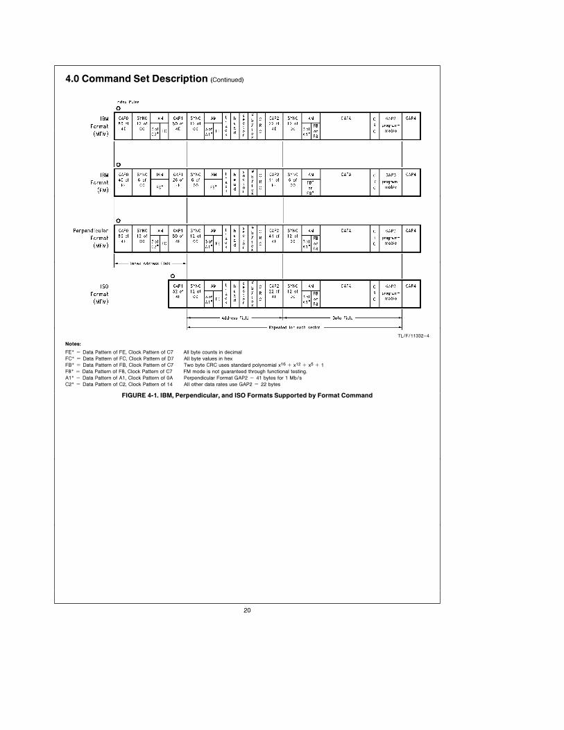
4.0 Command Set Description (Continued)
TL/F/11332–4
Notes:
FE* e Data Pattern of FE, Clock Pattern of C7 All byte counts in decimal
FC* e Data Pattern of FC, Clock Pattern of D7 All byte values in hex
FB* e Data Pattern of FB, Clock Pattern of C7 Two byte CRC uses standard polynomial x16 a x12 a x5 a 1
F8* e Data Pattern of F8, Clock Pattern of C7 FM mode is not guaranteed through functional testing.
A1* e Data Pattern of A1, Clock Pattern of 0A Perpendicular Format GAP2 e 41 bytes for 1 Mb/s
C2* e Data Pattern of C2, Clock Pattern of 14 All other data rates use GAP2 e 22 bytes
FIGURE 4-1. IBM, Perpendicular, and ISO Formats Supported by Format Command
20

4.0 Command Set Description (Continued)
The Format command terminates when the index hole is
detected a second time, at which point an interrupt is gener-
ated. Only the first three status bytes in the Result Phase
are significant. The Format Gap byte in the Command
Phase is dependent on the data rate and type of disk drive,
and will control the length of GAP3. Some typical values for
the programmable GAP3 are given in Table 4-1 below. Fig-ure 4-1 shows the track format for the different formats rec-
ognized by the Format Command.
4.2.4 Invalid Command
If an invalid command (illegal Opcode byte in the Command
Phase) is received by the controller, the controller will re-
spond with ST0 in the Result Phase. The controller does not
generate an interrupt during this condition. Bits 6 and 7 in
the MSR are both set to a 1, indicating to the mP that the
controller is in the Result Phase and the contents of ST0
must be read. The system will read an 80 (hex) value from
ST0 indicating an invalid command was received.
TABLE 4-1. Typical Format Gap Length Values
ModeSector Sector
EOTSector Format
Size Code Gap GAP3
Decimal Hex Hex Hex Hex
125 kb/s 128 00 12 07 09FM 128 00 10 10 19
256 01 08 18 30512 02 04 46 871024 03 02 C8 FF2048 04 01 C8 FF
250 kb/s 256 01 12 0A 0CMFM 256 01 10 20 32
512 02 08 2A 50512 02 09 2A 501024 03 04 80 F02048 04 02 C8 FF4096 05 01 C8 FF
250 kb/s 128 00 1A 07 1BFM 256 01 0F 0E 2A
512 02 08 1B 3A1024 03 04 47 8A2048 04 02 C8 FF4096 05 01 C8 FF
500 kb/s 256 01 1A 0E 36MFM 512 02 0F 1B 54
512 02 12 1B 6C1024 03 08 35 742048 04 04 99 FF4096 05 02 C8 FF8192 06 01 C8 FF
Note: FM mode is not guaranteed through functional testing.
Typical Values for PC Compatible Diskette Media
Media Sector SectorEOT
Sector Format
Type Size Code Gap GAP
Decimal Hex Hex Hex Hex
360K 512 02 09 2A 50
1.2M 512 02 0F 1B 54
720K 512 02 09 1B 50
1.44M 512 02 12 1B 6C
2.88M 512 02 24 1B 53
Notes:
Sector Gap refers to the Intersector Gap Length parameter specified in the Command Phase of the Read, Write, Scan, and Verify commands. Although this is the
recommended value, the PC8477B treats this byte as a don’t care in the Read, Write, Scan, and Verify commands.
Format Gap is the suggested value to use in the Format Gap parameter of the Format command. This is the programmable GAP3 as shown in Figure 4-1 .
The 2.88M diskette media is a new Barium Ferrite media intended for use in Perpendicular Recording drives at the data rate of up to 1 Mb/s.
21
4.0 Command Set Description (Continued)
4.2.5 Lock Command
The Lock command allows the user full control of the FIFO
parameters after a software reset. If the LOCK bit is set to 1,
then the FIFO, THRESH, and PRETRK bits in the Configure
command are not affected by a software reset. In addition,
the FWR, FRD, and BST bits in the Mode command will be
unaffected by a software reset. If the LOCK is 0 (default
after a hardware reset), then the above bits will be set to
their default values after a software reset. This command is
useful if the system designer wishes to keep the FIFO en-
abled and retain the other FIFO parameter values (such as
THRESH) after a software reset.
After the command byte is written, the result byte must be
read before continuing to the next command. The execution
of the Lock command is not performed until the result byte
is read by the mP. If the part is reset after the command byte
is written but before the result byte is read, then the Lock
command execution will not be performed. This is done to
prevent accidental execution of the Lock command.
4.2.6 Mode Command
This command is used to select the special features of the
controller. The bits for the Command Phase bytes are
shown in Section 4.1 Command Set Summary, and their
function is described below. These bits are set to their de-
fault values after a hardware reset. The default value of
each bit is denoted by a ‘‘bullet’’ to the left of each item. The
value of each parameter after a software reset will be ex-
plained.
TMR: Motor Timer mode. Default after a software reset.
# 0 e Timers for motor on and motor off are defined for
Mode 1. (See Specify command.) (default)
1 e Timers for motor on and motor off are defined for
Mode 2. (See Specify command.)
IAF: Index Address Format. Default after a software reset.
# 0 e The controller will format tracks with the Index Ad-
dress Field included. (IBM and Perpendicular for-
mat.)
1 e The controller will format tracks without including
the Index Address Field. (ISO format.)
IPS: Implied Seek. Default after a software reset.
# 0 e The implied seek bit in the command byte of a
read, write or scan is ignored. Implied seeks could
still be enabled by the EIS bit in the Configure
command.
1 e The IPS bit in the command byte of a read, write
or scan is enabled so that if it is set, the controller
will perform seek and sense interrupt operations
before executing the command.
LOW PWR: Low Power mode. Default after a software
reset.
# 00 e Completely disable the low power mode. (default)
01 e Automatic low power. Go into low power mode
512 ms after the head unload timer times out. This
is based on 500 kb/s or 1 Mb/s data rate. Double
this value for 250 kb/s.
10 e Manual low power. Go into low power mode now.
11 e Not used.
ETR: Extended Track Range. Default after a software reset.
# 0 e Track number is stored as a standard 8-bit value
compatible with the IBM, ISO, and Perpendicular
formats. This will allow access to up to 256 tracks
during a seek operation.
1 e Track number is stored as a 12-bit value. The up-
per four bits of the track value are stored in the
upper four bits of the head number in the sector
Address Field. This allows access to up to 4096
tracks during a seek operation. With this bit set, an
extra byte is required in the Seek Command
Phase and Sense Interrupt Result Phase.
FWR: FIFO Write Disable for mP write transfers to control-
ler. Default after a software reset if LOCK is 0. If LOCK is 1,
FWR will retain its value after a software reset.
Note: This bit is only valid if the FIFO is enabled in the Configure command.
If the FIFO is not enabled in the Configure command, then this bit is a
don’t care.
# 0 e Enable FIFO. Execution Phase mP write transfers
use the internal FIFO. (default)
1 e Disable FIFO. All write data transfers take place
without the FIFO.
FRD: FIFO Read Disable for mP read transfer from control-
ler. Default after a software reset if LOCK is 0. If LOCK is 1,
FRD will retain its value after a software reset.
Note: This bit is only valid if the FIFO is enabled in the Configure command.
If the FIFO is not enabled in the Configure command, then this bit is a
don’t care.
# 0 e Enable FIFO. Execution Phase mP read transfer
use the internal FIFO. (default)
1 e Disable FIFO. All read data transfers take place
without the FIFO.
BST: Burst Mode Disable. Default after a software reset if
LOCK is 0. If LOCK is 1, BST will retain its value after a
software reset.
Note: This bit is only valid if the FIFO is enabled in the Configure command.
If the FIFO is not enabled in the Configure command, then this bit is a
don’t care.
# 0 e Burst mode enabled for FIFO Execution Phase
data transfers. (default)
1 e Non-Burst mode enabled. The DRQ or INT pin will
be strobed once for each byte to be transferred
while the FIFO is enabled.
R255: Recalibrate Step Pulses. The bit will determine the
maximum number of recalibrate step pulses the controller
will issue before terminating with an error. Default after a
software reset.
# 0 e 85 maximum recalibrate step pulses. If ETR e 1,
controller will issue 3925 recalibrate step pulses
maximum.
1 e 255 maximum recalibrate step pulses. If ETR e 1,
controller will issue 4095 maximum recalibrate
step pulses.
DENSEL: Density Select Pin Configuration. This two bit val-
ue will configure the Density Select output to one of three
possible modes. The default mode will configure the DEN-
SEL pin according to the state of the IDENT input pin after a
data rate has been selected. That is, if IDENT is high, the
DENSEL pin is active high for the 500 kb/s or 1 Mb/s data
rates.
22

4.0 Command Set Description (Continued)
If IDENT is low, the DENSEL pin is active low for the
500 kb/s or 1 Mb/s data rates. In addition to these modes,
the DENSEL output can be set to always low or always high,
as shown in Table 4-2. This will allow the user more flexibili-
ty with new drive types.
Note: The DENSEL output values shown below are with the INVERT pin
tied low. If the INVERT pin is tied high, the outputs shown below have
the opposite polarity.
TABLE 4-2. DENSEL Decoding
Bit 1 Bit 0 DENSEL Pin Definition
0 0 low
0 1 high
1 0 undefined
1 1 DEFAULT
TABLE 4-3. DENSEL Default Encoding
Data RateDENSEL (default)
IDENT e 1 IDENT e 0
250 kb/s low high
300 kb/s low high
500 kb/s high low
1 Mb/s high low
BFR: CMOS Disk Interface Buffer Enable.
# 0 e Drive output signals configured as standard 4 mA
push-pull outputs (actually 48 mA sink, 4 mA
source). (default)
1 e Drive output signals configured as 48 mA open-
drain outputs.
WLD: Scan Wild Card.
# 0 e An FF (hex) from either the mP or the disk during a
Scan command is interpreted as a wildcard charac-
ter that will always match true. (default)
1 e The Scan commands do not recognize FF (hex) as
a wildcard character.
Head Settle: Time allowed for read/write head to settle af-
ter a seek during an Implied Seek operation.
Data Rate HST Range
250 kb/s N x 8 0–120 ms
300 kb/s N x 6.67 0–100 ms
500 kb/s N x 4 0–60 ms
1 Mb/s N x 2 0–30 ms
Note: N e 8 (default) HST e Head Settle Time
RG: Read Gate Diagnostic.
# 0 e Enable DSKCHG disk interface input for normal op-
eration. (default)
1 e Enable DSKCHG to act as an external Read Gate
input signal to the Data Separator. This is intended
as a test mode to aid in evaluation of the Data Sep-
arator.
PU: PUMP Pulse Output Diagnostic.
# 0 e Enable MFM output pin for normal operation. (de-
fault)
1 e Enable the MFM output to act as the active low out-
put of the Data Separator charge pump. This signal
consists of a series of pulses indicating when the
phase comparator is making a phase correction.
This Pump output will be active low for a pump up or
pump down signal from the phase comparator, and
is intended as a test mode to aid in the evaluation of
the Data Separator.
4.2.7 NSC Command
The NSC command can be used to distinguish between the
PC8477B version and the Intel 82077AA. The result Phase
byte uniquely identifies the floppy controller as a PC8477B,
which returns a value of 73 hex. The 82077AA and DP8473
return a value 80h signifying an invalid command. The lower
four bits of this result byte are subject to change by NSC,
and will reflect the particular version of the PC8477B part.
Note: The PC8477A will return a value of 72h in the result phase of the
NSC command.
4.2.8 Perpendicular Mode Command
The Perpendicular Mode command is designed to support
the unique Format and Write Data requirements of Perpen-
dicular (Vertical) Recording disk drives (4 Mbytes unformat-
ted capacity). The Perpendicular Mode command will con-
figure each of the four logical drives as a perpendicular or
conventional disk drive. Configuration of the four logical disk
drives is done via the D3–D0 bits, or with the GAP and WG
control bits. This command should be issued during the ini-
tialization of the floppy controller.
Perpendicular Recording drives operate in ‘‘Extra High Den-
sity’’ mode at 1 Mb/s, and are downward compatible with
1.44 Mbyte and 720 kbyte drives at 500 kb/s (High Density)
and 250 kb/s (Double Density) respectively. If perpendicular
drives are present in the system, this command should be
issued during initialization of the floppy controller, which will
configure each drive as perpendicular or conventional.
Then, when a drive is accessed for a Format or Write Data
command, the floppy controller will adjust the Format or
Write Data parameters based on the data rate (see Table
4-4).
Looking at the second command byte, DC3–DC0 corre-
spond to the four logical drives. A ‘‘0’’ written to DCn sets
drive n to conventional mode, and a ‘‘1’’ sets drive n to
perpendicular mode. Also, the OW (Overwrite) bit offers ad-
ditional control. When OW e 1, changing the values of
DC3–DC0 (drive configuration bits) is enabled. When
OW e 0, the internal values of DC3–DC0 are unaffected,
regardless of what is written to DC3–DC0.
The function of the DCn bits must also be qualified by set-
ting both WG and GAP to 0. If WG and GAP are used (i.e.,
not set to 00), they will override whatever is programmed in
the DCn bits. Table 4-4A indicates the operation of the
PC8477B based on the values of GAP and WG. Note that
when GAP and WG are both 0, the DCn bits are used to
configure each logical drive as conventional or perpendicu-
lar. DC3–DC0 are unaffected by a software reset, but WG
and GAP are both cleared to 0 after a software reset. A
hardware reset will reset all the bits to zero (conventional
mode for all drives). The Perpendicular Mode command bits
may be rewritten at any time.
Note: When in the Perpendicular Mode for any drive at any data rate via the
DC3–DC0 bits, write precompensation is set to zero.
23

4.0 Command Set Description (Continued)
TABLE 4-4. Effect of Drive Mode and Data Rate on Format and Write Commands
DriveGAP2 Length Portion of GAP2
Data RateMode
Written During Re-Written by Write
Format Data Command
250/300/500 kb/s Conventional 22 bytes 0 bytes
Perpendicular 22 bytes 19 bytes
1 Mb/s Conventional 22 bytes 0 bytes
Perpendicular 41 bytes 38 bytes
TABLE 4-4A. Effect of GAP and WG on Format and Write Commands
ModeGAP2 Length Portion of GAP2
GAP WGDescription
Written During Re-Written by Write
Format Data Command
0 0 Conventional 22 bytes 0 bytes
0 1 Perpendicular 22 bytes 19 bytes
(s500 kb/s)
1 0 Reserved 22 bytes 0 bytes
(Conventional)
1 1 Perpendicular 41 bytes 38 bytes
(1 Mb/s)
Perpendicular Recording type disk drives have a Pre-Erase
Head which leads the Read/Write Head by 200 mm, which
translates to 38 bytes at the 1 Mb/s data transfer rate (19
bytes at 500 kb/s). The increased spacing between the two
heads requires a larger GAP2 between the Address Field
and Data Field of a sector at 1 Mb/s. (See Perpendicular
Format in Table 4-1.) This GAP2 length of 41 bytes (at
1 Mb/s) will ensure that the Preamble in the Data Field is
completely ‘‘pre-erased’’ by the Pre-Erase Head. Also, dur-
ing Write Data operations to a perpendicular drive, a portion
of GAP2 must be rewritten by the controller to guarantee
that the Data Field Preamble has been pre-erased (see Ta-
ble 4-4).
4.2.9 Read Data Command
The Read Data command reads logical sectors containing a
Normal Data AM from the selected drive and makes the
data available to the host mP. After the last Command
Phase byte is written, the controller will simulate the Motor
On Time for the selected drive internally. The user must turn
on the drive motor directly by enabling the appropriate drive
and motor select disk interface outputs with the Digital Out-
put Register (DOR).
If Implied Seeks are enabled, the controller will perform a
Seek operation to the track number specified in the Com-
mand Phase. The controller will also issue a Sense Interrupt
for the seek and wait the Head Settle time specified in the
Mode command.
The correct ID information (track, head, sector, bytes per
sector) for the desired sector must be specified in the com-
mand bytes. See Table 4-5 Sector Size Selection for details
on the bytes per sector code. In addition, the End of Track
Sector Number (EOT) should be specified, allowing the con-
troller to read multiple sectors. The Data Length byte is a
don’t care and should be set to FF (hex).
TABLE 4-5. Sector Size Selection
Bytes per Number of Bytes
Sector Code in Data Field
0 128
1 256
2 512
3 1024
4 2048
5 4096
6 8192
7 16384
The controller then starts the Data Separator and waits for
the Data Separator to find the next sector Address Field.
The controller compares the Address Field ID information
(track, head, sector, bytes per sector) with the desired ID
specified in the Command Phase. If the sector ID bytes do
not match, then the controller waits for the Data Separator
to find the next sector Address Field. The ID comparison
process repeats until the Data Separator finds a sector Ad-
dress Field ID that matches that in the command bytes, or
until an error occurs. Possible errors are:
1. The mP aborted the command by writing to the FIFO. If
there is no disk in the drive, the controller will hang up.
The mP must then take the controller out of this hung
state by writing a byte to the FIFO. This will put the con-
troller into the Result Phase.
2. Two index pulses were detected since the search began,
and no valid ID has been found. If the track address ID
differs, the WT bit or BT bit (if the track address is FF hex)
will be set in ST2. If the head, sector, or bytes per sector
code did not match, the ND bit is set in ST1. If the Ad-
dress Field AM was never found, the MA bit is set in ST1.
3. The Address Field was found with a CRC error. The CE
bit is set in ST1.
24

4.0 Command Set Description (Continued)
Once the desired sector Address Field is found, the control-
ler waits for the Data Separator to find the subsequent Data
Field for that sector. If the Data Field (normal or deleted) is
not found with the expected time, the controller terminates
the operation and enters the Result Phase (MD is set in
ST2). If a Deleted Data Mark is found and SK was set in the
Opcode command byte, the controller skips this sector and
searches for the next sector Address Field as described
above. The effect of SK on the Read Data command is
summarized in Table 4-6.
Having found the Data Field, the controller then transfers
data bytes from the disk drive to the host (described in Sec-
tion 5.3 Controller Phases) until the bytes per sector count
has been reached, or the host terminates the operation
(through TC, end of track, or implicitly through overrun). The
controller will then generate the CRC for the sector and
compare this value with the CRC at the end of the Data
Field.
Having finished reading the sector, the controller will contin-
ue reading the next logical sector unless one or more of the
following termination conditions occurred:
1. The DMA controller asserted TC. The IC bits in ST0 are
set to Normal Termination.
2. The last sector address (of side 1 if MT was set) was
equal to EOT. The EOT bit in ST1 is set. The IC bits in
ST0 are set to Abnormal Termination. This is the expect-
ed condition during Non-DMA transfers.
3. Overrun error. The OR bit in ST1 is set. The IC bits in ST0
are set to Abnormal Termination. If the mP cannot service
a transfer request in time, the last correctly read byte will
be transferred.
4. CRC error. The CE bit in ST1 and CD bit in ST2 are set.
The IC bits in ST0 are set to Abnormal Termination.
If MT was set in the Opcode command byte, and the last
sector of side 0 has been transferred, the controller will then
continue with side 1, starting with sector 1 and continuing
until EOT sector number is reached or TC occurs.
Upon terminating the Execution Phase of the Read Data
command, the controller will assert INT, indicating the be-
ginning of the Result Phase. The mP must then read the
result bytes from the FIFO. The values that will be read back
in the result bytes are shown in Table 4-7. If an error occurs,
the result bytes will indicate the sector read when the error
occurred.
4.2.10 Read Deleted Data Command
The Read Deleted Data command reads logical sectors
containing a Deleted Data AM from the selected drive and
makes the data available to the host mP. This command is
identical to the Read Data command, except for the setting
of the CM bit in ST2 and the skipping of sectors. The effect
of SK on the Read Deleted Data command is summarized in
Table 4-8. See Table 4-7 for the state of the result bytes for
a Normal Termination of the command.
TABLE 4-6. SK Effect on Read Data Command
SK Data Type Sector Read? CM Bit (ST2) Description of Results
0 Normal Y 0 Normal Termination
0 Deleted Y 1 No Further Sectors Read
1 Normal Y 0 Normal Termination
1 Deleted N 1 Sector Skipped
TABLE 4-7. Result Phase Termination Values with No Error
MT HD Last SectorID Information at Result Phase
Track Head Sector Bytes/Sector
0 0 k EOT NC NC S a 1 NC
0 0 e EOT T a 1 NC 1 NC
0 1 k EOT NC NC S a 1 NC
0 1 e EOT T a 1 NC 1 NC
1 0 k EOT NC H S a 1 NC
1 0 e EOT T a 1 0 1 NC
1 1 k EOT NC H S a 1 NC
1 1 e EOT T a 1 0 1 NC
EOT e End of Track Sector Number from Command Phase
NC e No Change in Value
S e Sector Number last operated on by controller
T e Track Number programmed in Command Phase
H e Head last selected by controller
TABLE 4-8. SK Effect on Read Deleted Data Command
SK Data Type Sector Read? CM Bit (ST2) Description of Results
0 Normal Y 1 No Further Sectors Read
0 Deleted Y 0 Normal Termination
1 Normal N 1 Sector Skipped
1 Deleted Y 0 Normal Termination
25
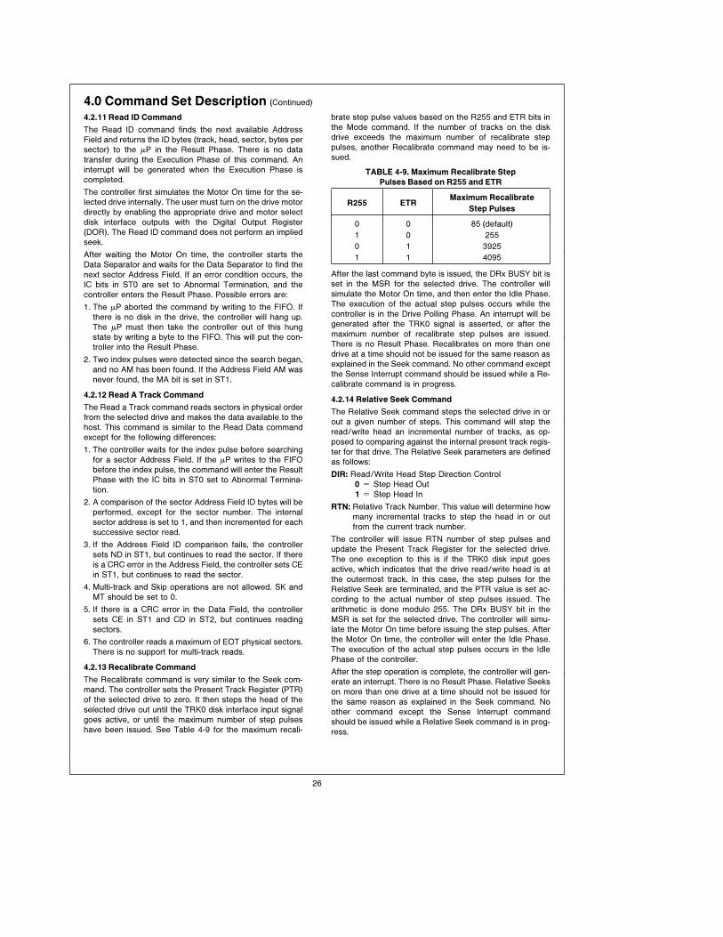
4.0 Command Set Description (Continued)
4.2.11 Read ID Command
The Read ID command finds the next available Address
Field and returns the ID bytes (track, head, sector, bytes per
sector) to the mP in the Result Phase. There is no data
transfer during the Execution Phase of this command. An
interrupt will be generated when the Execution Phase is
completed.
The controller first simulates the Motor On time for the se-
lected drive internally. The user must turn on the drive motor
directly by enabling the appropriate drive and motor select
disk interface outputs with the Digital Output Register
(DOR). The Read ID command does not perform an implied
seek.
After waiting the Motor On time, the controller starts the
Data Separator and waits for the Data Separator to find the
next sector Address Field. If an error condition occurs, the
IC bits in ST0 are set to Abnormal Termination, and the
controller enters the Result Phase. Possible errors are:
1. The mP aborted the command by writing to the FIFO. If
there is no disk in the drive, the controller will hang up.
The mP must then take the controller out of this hung
state by writing a byte to the FIFO. This will put the con-
troller into the Result Phase.
2. Two index pulses were detected since the search began,
and no AM has been found. If the Address Field AM was
never found, the MA bit is set in ST1.
4.2.12 Read A Track Command
The Read a Track command reads sectors in physical order
from the selected drive and makes the data available to the
host. This command is similar to the Read Data command
except for the following differences:
1. The controller waits for the index pulse before searching
for a sector Address Field. If the mP writes to the FIFO
before the index pulse, the command will enter the Result
Phase with the IC bits in ST0 set to Abnormal Termina-
tion.
2. A comparison of the sector Address Field ID bytes will be
performed, except for the sector number. The internal
sector address is set to 1, and then incremented for each
successive sector read.
3. If the Address Field ID comparison fails, the controller
sets ND in ST1, but continues to read the sector. If there
is a CRC error in the Address Field, the controller sets CE
in ST1, but continues to read the sector.
4. Multi-track and Skip operations are not allowed. SK and
MT should be set to 0.
5. If there is a CRC error in the Data Field, the controller
sets CE in ST1 and CD in ST2, but continues reading
sectors.
6. The controller reads a maximum of EOT physical sectors.
There is no support for multi-track reads.
4.2.13 Recalibrate Command
The Recalibrate command is very similar to the Seek com-
mand. The controller sets the Present Track Register (PTR)
of the selected drive to zero. It then steps the head of the
selected drive out until the TRK0 disk interface input signal
goes active, or until the maximum number of step pulses
have been issued. See Table 4-9 for the maximum recali-
brate step pulse values based on the R255 and ETR bits in
the Mode command. If the number of tracks on the disk
drive exceeds the maximum number of recalibrate step
pulses, another Recalibrate command may need to be is-
sued.
TABLE 4-9. Maximum Recalibrate Step
Pulses Based on R255 and ETR
R255 ETRMaximum Recalibrate
Step Pulses
0 0 85 (default)
1 0 255
0 1 3925
1 1 4095
After the last command byte is issued, the DRx BUSY bit is
set in the MSR for the selected drive. The controller will
simulate the Motor On time, and then enter the Idle Phase.
The execution of the actual step pulses occurs while the
controller is in the Drive Polling Phase. An interrupt will be
generated after the TRK0 signal is asserted, or after the
maximum number of recalibrate step pulses are issued.
There is no Result Phase. Recalibrates on more than one
drive at a time should not be issued for the same reason as
explained in the Seek command. No other command except
the Sense Interrupt command should be issued while a Re-
calibrate command is in progress.
4.2.14 Relative Seek Command
The Relative Seek command steps the selected drive in or
out a given number of steps. This command will step the
read/write head an incremental number of tracks, as op-
posed to comparing against the internal present track regis-
ter for that drive. The Relative Seek parameters are defined
as follows:
DIR: Read/Write Head Step Direction Control
0 e Step Head Out
1 e Step Head In
RTN: Relative Track Number. This value will determine how
many incremental tracks to step the head in or out
from the current track number.
The controller will issue RTN number of step pulses and
update the Present Track Register for the selected drive.
The one exception to this is if the TRK0 disk input goes
active, which indicates that the drive read/write head is at
the outermost track. In this case, the step pulses for the
Relative Seek are terminated, and the PTR value is set ac-
cording to the actual number of step pulses issued. The
arithmetic is done modulo 255. The DRx BUSY bit in the
MSR is set for the selected drive. The controller will simu-
late the Motor On time before issuing the step pulses. After
the Motor On time, the controller will enter the Idle Phase.
The execution of the actual step pulses occurs in the Idle
Phase of the controller.
After the step operation is complete, the controller will gen-
erate an interrupt. There is no Result Phase. Relative Seeks
on more than one drive at a time should not be issued for
the same reason as explained in the Seek command. No
other command except the Sense Interrupt command
should be issued while a Relative Seek command is in prog-
ress.
26
4.0 Command Set Description (Continued)
4.2.15 Scan Commands
The Scan commands allow data read from the disk to be
compared against data sent from the mP. There are three
Scan commands to choose from:
Scan Equal Disk Data e mP Data
Scan Low or Equal Disk Data s mP Data
Scan High or Equal Disk Data t mP Data
Each sector is interpreted with the most significant bytes
first. If the Wildcard mode is enabled in the Mode command,
an FF (hex) from either the disk or the mP is used as a don’t
care byte that will always match equal. After each sector is
read, if the desired condition has not been met, the next
sector is read. The next sector is defined as the current
sector number plus the Sector Step Size specified. The
Scan command will continue until the scan condition has
been met, or the EOT has been reached, or if TC is assert-
ed.
Read errors on the disk will have the same error conditions
as the Read Data command. If the SK bit is set, sectors with
deleted data marks are ignored. If all sectors read are
skipped, the command will terminate with D3 of ST2 set
(Scan Equal Hit). The Result Phase of the command is
shown in Table 4-10.
TABLE 4-10. Scan Command Termination Values
Command
Status
ConditionsRegister 2
D2 D3
Scan Equal 0 1 Disk e mP
1 0 Disk i mP
Scan Low 0 1 Disk e mP
or Equal 0 0 Disk k mP
1 0 Disk l mP
Scan High 0 1 Disk e mP
or Equal 0 0 Disk k mP
1 0 Disk l mP
4.2.16 Seek Command
The Seek command issues step pulses to move the select-
ed drive head in or out until the desired track number is
reached. During the Execution Phase of the Seek com-
mand, the track number to seek to is compared with the
present track number. The controller will determine how
many step pulses to issue and the DIR disk interface output
will indicate which direction the R/W head should move.
The DRx BUSY bit is set in the MSR for the appropriate
drive. The controller will wait the Motor On time before issu-
ing the first step pulse.
After the Motor On time, the controller will enter the Idle
Phase. The execution of the actual step pulses occurs in the
Drive Polling phase of the controller. The step pulse rate is
determined by the value programmed in the Specify com-
mand. An interrupt will be generated one step pulse period
after the last step pulse is issued. There is no Result Phase.
A Sense Interrupt command should be issued to determine
the cause of the interrupt.
While the internal microengine is capable of multiple seeks
on 2 or more drives at the same time, software should en-
sure that only one drive is seeking or recalibrating at a time.
This is because the drives are actually selected via the
DOR, which can only select one drive at a time. No other
command except a Sense Interrupt command should be is-
sued while a Seek command is in progress.
If the extended track range mode is enabled with the ETR
bit in the Mode command, a fourth command byte should be
written in the Command Phase to indicate the four most
significant bits of the desired track number. Otherwise, only
three command bytes should be written.
4.2.17 Sense Drive Status Command
The Sense Drive Status command returns the status of the
selected disk drive in ST3. This command does not gener-
ate an interrupt.
4.2.18 Sense Interrupt Command
The Sense Interrupt command is used to determine the
cause of interrupt when the interrupt is a result of the
change in status of any disk drive. Four possible causes of
the interrupt are:
1. Upon entering the Result Phase of:
a. Read Data command
b. Read Deleted Data command
c. Read a Track command
d. Read ID command
e. Write Data command
f. Write Deleted Data command
g. Format command
h. Scan command
i. Verify command
2. During data transfers in the Execution Phase while in the
Non-DMA mode.
3. Ready Changed State during the polling mode for an in-
ternally selected drive. (Occurs only after a hardware or
software reset.)
4. Seek, Relative Seek, or Recalibrate termination.
An interrupt due to reasons 1 and 2 does not require the
Sense Interrupt command and is cleared automatically. This
interrupt occurs during normal command operations and is
easily discernible by the mP via the MSR. This interrupt is
cleared reading or writing information from/to the Data Reg-
ister (FIFO).
Interrupts caused by reason 3 and 4 are identified with the
aid of the Sense Interrupt command. The interrupt is cleared
after the first result byte has been read. Use bits 5, 6, and 7
of ST0 to identify the cause of the interrupt as shown in
Table 4-11.
TABLE 4-11. Status Register 0 Termination Codes
Status Register 0
CauseInterrupt Seek
Code End
D7 D6 D5
1 1 0 Internal Ready Went True
0 0 1 Normal Seek Termination
0 1 1 Abnormal Seek Termination
Issuing a Sense Interrupt command without an interrupt
pending is treated as an Invalid command. If the extended
track range mode is enabled, a third byte should be read in
the Result Phase, which will indicate the four most signifi-
cant bits of the present track number. Otherwise, only two
result bytes should be read.
27
4.0 Command Set Description (Continued)
4.2.19 Set Track Command
This command is used to inspect or change the value of the
internal Present Track Register. This could be useful for re-
covery from disk mis-tracking errors, where the real current
track could be read through the Read ID command, and
then the Set Track command could be used to set the inter-
nal Present Track Register to the correct value.
If the WNR bit is a 0, a track register is to be read. In this
case, the Result Phase byte contains the value in the inter-
nal register specified, and the third byte in the Command
Phase is a dummy byte.
If the WNR bit is a 1, data is written to a track register. In this
case the third byte of the Command Phase is written to the
specified internal track register, and the Result Phase byte
contains this new value written.
The DS1 and DS0 bits select the Present Track Register for
the particular drive. The internal register address depends
on MSB, DS1, and DS0 as shown in Table 4-12. This com-
mand does not generate an interrupt.
TABLE 4-12. Set Track Register Address
DS1 DS0 MSB Register Addressed
0 0 0 PTR0(LSB)
0 0 1 PTR0(MSB)
0 1 0 PTR1(LSB)
0 1 1 PTR1(MSB)
1 0 0 PTR2(LSB)
1 0 1 PTR2(MSB)
1 1 0 PTR3(LSB)
1 1 1 PTR3(MSB)
4.2.20 Specify Command
The Specify command sets the initial values for three inter-
nal timers. The function of these Specify parameters is de-
scribed below. The parameters of this command are unde-
fined after power up, and are unaffected by any reset. Thus,
software should always issue a Specify command as part of
an initialization routine. This command does not generate
an interrupt.
The Motor Off and Motor On timers are artifacts of the
mPD765. These timers determine the delay from selecting a
drive motor until a read or write operation is started, and the
delay of deselecting the drive motor after the command is
completed. Since the PC8477B enables the drive and motor
select line directly through the DOR, these timers only pro-
vide some delay from the initiation of a command until it is
actually started.
Step Rate Time: These four bits define the time interval
between successive step pulses during a seek, implied
seek, recalibrate, or relative seek. The programming of this
step rate is shown in Table 4-13.
TABLE 4-13. Step Rate Time (SRT) Values
Data Rate Value Range Units
1 Mb/s (16-SRT) x 0.5 0.5–8 ms
500 kb/s (16-SRT) 1–16 ms
300 kb/s (16-SRT) x 1.67 1.67–26.7 ms
250 kb/s (16-SRT) x 2 2–32 ms
Motor Off Time: These four bits determine the simulated
Motor Off time as shown in Table 4-14.
TABLE 4-14. Motor Off Time (MFT) Values
Rate
Data Mode 1 (TMR e 0) Mode 2 (TMR e 1)Units
Value Range Value Range
1 Mb/s MFT x 8 8–128 MFT x 512 512–8192 ms
500 kb/s MFT x 16 16–256 MFT x 512 512–8192 ms
300 kb/s MFT x 80/3 26.7–427 MFT x 2560/3 853–13653 ms
250 kb/s MFT x 32 32–512 MFT x 1024 1024–16384 ms
Note: MFT e 0 is treated as Motor Off Time e 16.
Motor On Time: These seven bits determine the simulated
Motor On time as shown in Table 4-15.
TABLE 4-15. Motor On Time (MNT) Values
Rate
Data Mode 1 (TMR e 0) Mode 2 (TMR e 1)Units
Value Range Value Range
1 Mb/s MNT 1–128 MNT x 32 32–4096 ms
500 kb/s MNT 1–128 MNT x 32 32–4096 ms
300 kb/s MNT x 10/3 3.3–427 MNT x 160/3 53–6827 ms
250 kb/s MNT x 4 4–512 MNT x 64 64–8192 ms
Note 1: MNT e 0 is treated as Motor On Time e 128.
Note 2: For PC8477A at 500 kb/s when TMR e 0 the value is MNT x 2 and
range is 2–256.
DMA: This bit selects the data transfer mode in the Execu-
tion Phase of a read, write, or scan operation.
0 DMA mode is selected.
1 Non-DMA mode is selected.
4.2.21 Verify Command
The Verify command reads logical sectors containing a Nor-
mal Data AM from the selected drive without transferring
the data to the host. This command is identical to the Read
Data command, except that no data is transferred during
the Execution Phase.
The Verify command is designed for post-format or post-
write verification. Data is read from the disk, as the control-
ler checks for valid Address Marks in the Address and Data
Fields. The CRC is computed and checked against the pre-
viously stored value on the disk. The EOT value should be
set to the final sector to be checked on each side. If EOT is
greater than the number of sectors per side, the command
will terminate with an error and no useful Address Mark or
CRC data will be given.
The TC pin cannot be used to terminate this command
since no data is transferred. The command can simulate a
TC by setting the EC bit to a 1. In this case, the command
will terminate when SC (Sector Count) sectors have been
read. (If SC e 0 then 256 sectors will be verified.) If EC e
0, then the command will terminate when EOT is equal to
the last sector to be checked. In this case, the Data Length
parameter should be set to FF hex. Refer to Table 4-7 for
the Result Phase values for a successful completion of the
command. Also see Table 4-16 for further explanation of
the result bytes with respect to the MT and EC bits.
28
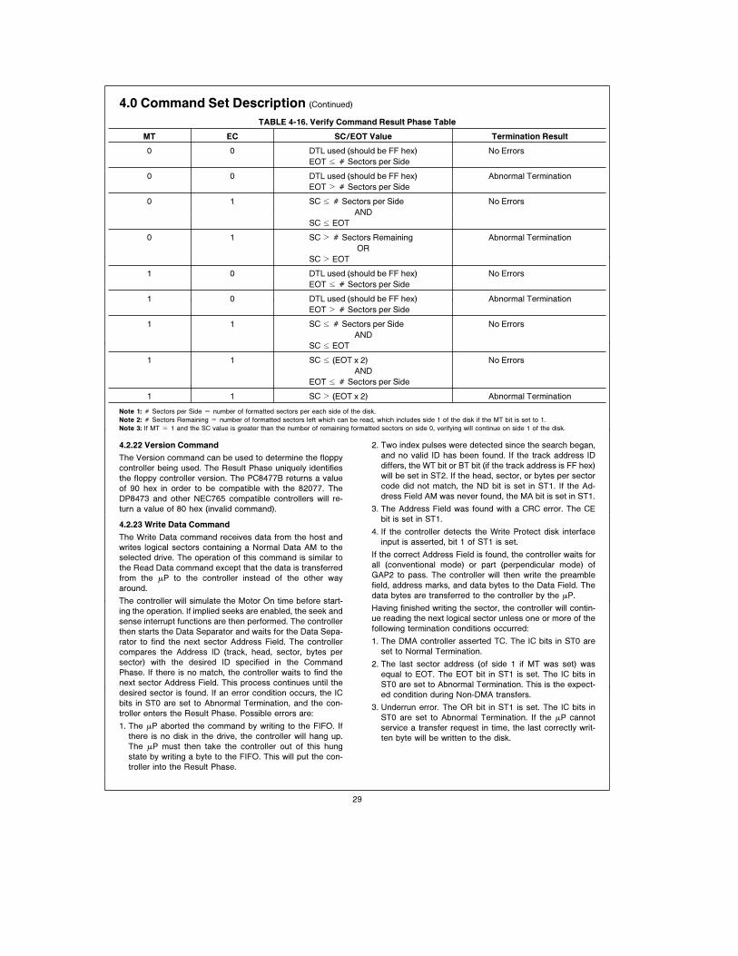
4.0 Command Set Description (Continued)
TABLE 4-16. Verify Command Result Phase Table
MT EC SC/EOT Value Termination Result
0 0 DTL used (should be FF hex) No Errors
EOT s Ý Sectors per Side
0 0 DTL used (should be FF hex) Abnormal Termination
EOT l Ý Sectors per Side
0 1 SC s Ý Sectors per Side No Errors
AND
SC s EOT
0 1 SC l Ý Sectors Remaining Abnormal Termination
OR
SC l EOT
1 0 DTL used (should be FF hex) No Errors
EOT s Ý Sectors per Side
1 0 DTL used (should be FF hex) Abnormal Termination
EOT l Ý Sectors per Side
1 1 SC s Ý Sectors per Side No Errors
AND
SC s EOT
1 1 SC s (EOT x 2) No Errors
AND
EOT s Ý Sectors per Side
1 1 SC l (EOT x 2) Abnormal Termination
Note 1: Ý Sectors per Side e number of formatted sectors per each side of the disk.
Note 2: Ý Sectors Remaining e number of formatted sectors left which can be read, which includes side 1 of the disk if the MT bit is set to 1.
Note 3: If MT e 1 and the SC value is greater than the number of remaining formatted sectors on side 0, verifying will continue on side 1 of the disk.
4.2.22 Version Command
The Version command can be used to determine the floppy
controller being used. The Result Phase uniquely identifies
the floppy controller version. The PC8477B returns a value
of 90 hex in order to be compatible with the 82077. The
DP8473 and other NEC765 compatible controllers will re-
turn a value of 80 hex (invalid command).
4.2.23 Write Data Command
The Write Data command receives data from the host and
writes logical sectors containing a Normal Data AM to the
selected drive. The operation of this command is similar to
the Read Data command except that the data is transferred
from the mP to the controller instead of the other way
around.
The controller will simulate the Motor On time before start-
ing the operation. If implied seeks are enabled, the seek and
sense interrupt functions are then performed. The controller
then starts the Data Separator and waits for the Data Sepa-
rator to find the next sector Address Field. The controller
compares the Address ID (track, head, sector, bytes per
sector) with the desired ID specified in the Command
Phase. If there is no match, the controller waits to find the
next sector Address Field. This process continues until the
desired sector is found. If an error condition occurs, the IC
bits in ST0 are set to Abnormal Termination, and the con-
troller enters the Result Phase. Possible errors are:
1. The mP aborted the command by writing to the FIFO. If
there is no disk in the drive, the controller will hang up.
The mP must then take the controller out of this hung
state by writing a byte to the FIFO. This will put the con-
troller into the Result Phase.
2. Two index pulses were detected since the search began,
and no valid ID has been found. If the track address ID
differs, the WT bit or BT bit (if the track address is FF hex)
will be set in ST2. If the head, sector, or bytes per sector
code did not match, the ND bit is set in ST1. If the Ad-
dress Field AM was never found, the MA bit is set in ST1.
3. The Address Field was found with a CRC error. The CE
bit is set in ST1.
4. If the controller detects the Write Protect disk interface
input is asserted, bit 1 of ST1 is set.
If the correct Address Field is found, the controller waits for
all (conventional mode) or part (perpendicular mode) of
GAP2 to pass. The controller will then write the preamble
field, address marks, and data bytes to the Data Field. The
data bytes are transferred to the controller by the mP.
Having finished writing the sector, the controller will contin-
ue reading the next logical sector unless one or more of the
following termination conditions occurred:
1. The DMA controller asserted TC. The IC bits in ST0 are
set to Normal Termination.
2. The last sector address (of side 1 if MT was set) was
equal to EOT. The EOT bit in ST1 is set. The IC bits in
ST0 are set to Abnormal Termination. This is the expect-
ed condition during Non-DMA transfers.
3. Underrun error. The OR bit in ST1 is set. The IC bits in
ST0 are set to Abnormal Termination. If the mP cannot
service a transfer request in time, the last correctly writ-
ten byte will be written to the disk.
29
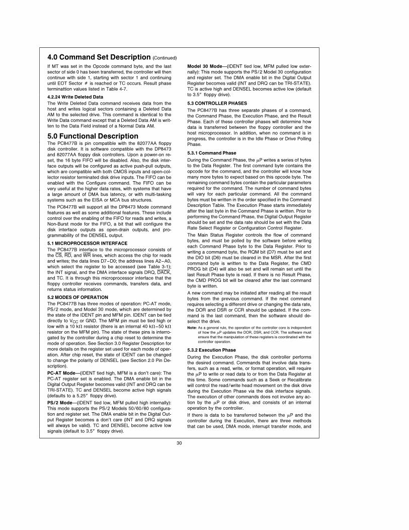
4.0 Command Set Description (Continued)
If MT was set in the Opcode command byte, and the last
sector of side 0 has been transferred, the controller will then
continue with side 1, starting with sector 1 and continuing
until EOT Sector Ý is reached or TC occurs. Result phase
terminattion values listed in Table 4-7.
4.2.24 Write Deleted Data
The Write Deleted Data command receives data from the
host and writes logical sectors containing a Deleted Data
AM to the selected drive. This command is identical to the
Write Data command except that a Deleted Data AM is writ-
ten to the Data Field instead of a Normal Data AM.
5.0 Functional DescriptionThe PC8477B is pin compatible with the 82077AA floppy
disk controller. It is software compatible with the DP8473
and 82077AA floppy disk controllers. Upon a power-on re-
set, the 16 byte FIFO will be disabled. Also, the disk inter-
face outputs will be configured as active push-pull outputs,
which are compatible with both CMOS inputs and open-col-
lector resistor terminated disk drive inputs. The FIFO can be
enabled with the Configure command. The FIFO can be
very useful at the higher data rates, with systems that have
a large amount of DMA bus latency, or with multi-tasking
systems such as the EISA or MCA bus structures.
The PC8477B will support all the DP8473 Mode command
features as well as some additional features. These include
control over the enabling of the FIFO for reads and writes, a
Non-Burst mode for the FIFO, a bit that will configure the
disk interface outputs as open-drain outputs, and pro-
grammability of the DENSEL output.
5.1 MICROPROCESSOR INTERFACE
The PC8477B interface to the microprocessor consists of
the CS, RD, and WR lines, which access the chip for reads
and writes; the data lines D7–D0; the address lines A2–A0,
which select the register to be accessed (see Table 3-1);
the INT signal, and the DMA interface signals DRQ, DACK,
and TC. It is through this microprocessor interface that the
floppy controller receives commands, transfers data, and
returns status information.
5.2 MODES OF OPERATION
The PC8477B has three modes of operation: PC-AT mode,
PS/2 mode, and Model 30 mode, which are determined by
the state of the IDENT pin and MFM pin. IDENT can be tied
directly to VCC or GND. The MFM pin must be tied high or
low with a 10 kX resistor (there is an internal 40 kX–50 kXresistor on the MFM pin). The state of these pins is interro-
gated by the controller during a chip reset to determine the
mode of operation. See Section 3.0 Register Description for
more details on the register set used for each mode of oper-
ation. After chip reset, the state of IDENT can be changed
to change the polarity of DENSEL (see Section 2.0 Pin De-
scription).
PC-AT ModeÐ(IDENT tied high, MFM is a don’t care): The
PC-AT register set is enabled. The DMA enable bit in the
Digital Output Register becomes valid (INT and DRQ can be
TRI-STATE). TC and DENSEL become active high signals
(defaults to a 5.25× floppy drive).
PS/2 ModeÐ(IDENT tied low, MFM pulled high internally):
This mode supports the PS/2 Models 50/60/80 configura-
tion and register set. The DMA enable bit in the Digital Out-
put Register becomes a don’t care (INT and DRQ signals
will always be valid). TC and DENSEL become active low
signals (default to 3.5× floppy drive).
Model 30 ModeÐ(IDENT tied low, MFM pulled low exter-
nally): This mode supports the PS/2 Model 30 configuration
and register set. The DMA enable bit in the Digital Output
Register becomes valid (INT and DRQ can be TRI-STATE).
TC is active high and DENSEL becomes active low (default
to 3.5× floppy drive).
5.3 CONTROLLER PHASES
The PC8477B has three separate phases of a command,
the Command Phase, the Execution Phase, and the Result
Phase. Each of these controller phases will determine how
data is transferred between the floppy controller and the
host microprocessor. In addition, when no command is in
progress, the controller is in the Idle Phase or Drive Polling
Phase.
5.3.1 Command Phase
During the Command Phase, the mP writes a series of bytes
to the Data Register. The first command byte contains the
opcode for the command, and the controller will know how
many more bytes to expect based on this opcode byte. The
remaining command bytes contain the particular parameters
required for the command. The number of command bytes
will vary for each particular command. All the command
bytes must be written in the order specified in the Command
Description Table. The Execution Phase starts immediately
after the last byte in the Command Phase is written. Prior to
performing the Command Phase, the Digital Output Register
should be set and the data rate should be set with the Data
Rate Select Register or Configuration Control Register.
The Main Status Register controls the flow of command
bytes, and must be polled by the software before writing
each Command Phase byte to the Data Register. Prior to
writing a command byte, the RQM bit (D7) must be set and
the DIO bit (D6) must be cleared in the MSR. After the first
command byte is written to the Data Register, the CMD
PROG bit (D4) will also be set and will remain set until the
last Result Phase byte is read. If there is no Result Phase,
the CMD PROG bit will be cleared after the last command
byte is written.
A new command may be initiated after reading all the result
bytes from the previous command. If the next command
requires selecting a different drive or changing the data rate,
the DOR and DSR or CCR should be updated. If the com-
mand is the last command, then the software should de-
select the drive.
Note: As a general rule, the operation of the controller core is independent
of how the mP updates the DOR, DSR, and CCR. The software must
ensure that the manipulation of these registers is coordinated with the
controller operation.
5.3.2 Execution Phase
During the Execution Phase, the disk controller performs
the desired command. Commands that involve data trans-
fers, such as a read, write, or format operation, will require
the mP to write or read data to or from the Data Register at
this time. Some commands such as a Seek or Recalibrate
will control the read/write head movement on the disk drive
during the Execution Phase via the disk interface signals.
The execution of other commands does not involve any ac-
tion by the mP or disk drive, and consists of an internal
operation by the controller.
If there is data to be transferred between the mP and the
controller during the Execution, there are three methods
that can be used, DMA mode, interrupt transfer mode, and
30

5.0 Functional Description (Continued)
software polling mode. The last two modes are called the
Non-DMA modes. The DMA mode is used if the system has
a DMA controller. This allows the mP to do other tasks while
the data transfer takes place during the Execution Phase. If
the Non-DMA mode is used, an interrupt is issued for each
byte transferred during the Execution Phase. Also, instead
of using the interrupt during Non-DMA mode, the Main
Status Register can be polled by software to indicate when
a byte transfer is required. All of these data transfer modes
will work with the FIFO enabled or disabled.
5.3.2.1 DMA ModeÐFIFO Disabled
The DMA mode is selected by writing a 0 to the DMA bit in
the Specify command and by setting the DMA enabled bit
(D3) in the DOR. With the FIFO disabled, a DMA request
(DRQ) is generated in the Execution Phase when each byte
is ready to be transferred. The DMA controller should re-
spond in the DRQ with a DMA acknowledge (DACK) and a
read or write strobe. The DRQ will be cleared by the leading
edge of the active low DACK input signal. After the last byte
is transferred, an interrupt is generated, indicating the begin-
ning of the Result Phase. During DMA operations the chip
select input (CS) must be held high. The DACK signal will
act as the chip select for the FIFO in this case, and the state
of the address lines A2–A0 is a don’t care. The Terminal
Count (TC) signal can be asserted by the DMA controller to
terminate the data transfer at any time. Due to internal gat-
ing, TC is only recognized when DACK is low.
PC-AT Mode: When in the PC-AT interface mode with the
FIFO disabled, the controller will be in single byte transfer
mode. That is, the system will have one byte time to service
a DMA request (DRQ) from the controller. DRQ will be deas-
serted between each byte.
PS/2 and Model 30 Modes: When in the PS/2 or Model 30
modes, DMA transfers with the FIFO disabled are per-
formed differently. Instead of a single byte transfer mode,
the FIFO will actually be enabled with THRESH e 0F (hex).
Thus, DRQ will be asserted when one byte has entered the
FIFO during reads, and when one byte can be written to the
FIFO during writes. DRQ will be deasserted by the leading
edge of the DACK input, and will be reasserted when DACK
goes inactive high. This operation is very similar to Burst
mode transfer with the FIFO enabled except that DRQ is
deasserted between each byte.
5.3.2.2 DMA ModeÐFIFO Enabled
Read Data Transfers
Whenever the number of bytes in the FIFO is greater than
or equal to (16bTHRESH), a DRQ is generated. This is the
trigger condition for the FIFO read data transfers from the
floppy controller to the mP.
Burst Mode: DRQ will remain active until enough bytes
have been read from the controller to empty the FIFO.
Non-Burst Mode: DRQ will be deasserted after each read
transfer. If the FIFO is not completely empty, DRQ will be
reasserted after a 350 ns delay. This will allow other higher
priority DMA transfers to take place between floppy trans-
fers. In addition, this mode will allow the controller to work
correctly in systems where the DMA controller is put into a
read verify mode, where only DACK signals are sent to the
FDC, with no RD pulses. This read verify mode of the DMA
controller is used in some PC software. The FIFO Non-Burst
mode allows the DACK input from the DMA controller to be
strobed, which will correctly clock data from the FIFO.
For both the Burst and Non-Burst modes, when the last byte
in the FIFO has been read, DRQ will go inactive. DRQ will
then be reasserted when the FIFO trigger condition is satis-
fied. After the last byte of a sector has been read from the
disk, DRQ is again generated even if the FIFO has not yet
reached its threshold trigger condition. This will guarantee
that all the current sector bytes are read from the FIFO
before the next sector byte transfer begins.
Write Data Transfers
Whenever the number of bytes in the FIFO is less than or
equal to THRESH, a DRQ is generated. This is the trigger
condition for the FIFO write data transfers from the mP to
the floppy controller.
Burst Mode: DRQ will remain active until enough bytes
have been written to the controller to completely fill the
FIFO.
Non-Burst Mode: DRQ will be deasserted after each write
transfer. If the FIFO is not yet full, DRQ will be reasserted
after a 350 ns delay. This deassertion of DRQ will allow
other higher priority DMA transfers to take place between
floppy transfers.
The FIFO has a byte counter which will monitor the number
of bytes being transferred to the FIFO during write opera-
tions for both Burst and Non-Burst modes. When the last
byte of a sector is transferred to the FIFO, DRQ will be
deasserted even if the FIFO has not been completely filled.
In this way, the FIFO will be cleared after each sector is
written. Only after the floppy controller has determined that
another sector is to be written will DRQ be asserted again.
Also, since DRQ is deasserted immediately after the last
byte of a sector is written to the FIFO, the system does not
need to tolerate any DRQ deassertion delay and is free to
do other work.
Read and Write Data Transfers
The DACK input signal from the DMA controller may be held
active during an entire burst or it may be strobed for each
byte transferred during a read or write operation. When in
the Burst mode, the floppy controller will deassert DRQ as
soon as it recognizes that the last byte of a burst was trans-
ferred. If DACK is strobed for each byte, the leading edge of
this strobe is used to deassert DRQ. If DACK is strobed, RD
or WR are not required. This is the case during the Read
Verify mode of the DMA Controller. If DACK is held active
during the entire burst, the trailing edge of the RD or WR
strobe is used to deassert DRQ. DRQ will be deasserted
within 50 ns of the leading edge of DACK, RD, or WR. This
quick response should prevent the DMA controller from
transferring extra bytes in most applications.
Overrun Errors
An overrun or underrun error will terminate the execution of
the command if the system does not transfer data within the
allotted data transfer time (see Section 3.7), which will put
the controller into the Result Phase. During a read overrun,
the mP is required to read the remaining bytes of the sector
before the controller will assert INT, signifying the end of
execution. During a write operation, an underrun error will
terminate the Execution Phase after the controller has writ-
ten the remaining bytes of the sector with the last correctly
written byte to the FIFO and generated the CRC bytes.
Whether there is an error or not, an interrupt is generated at
the end of the Execution Phase, and is cleared by reading
the first Result Phase byte.
31
5.0 Functional Description (Continued)
DACK asserted by itself without a RD or WR strobe is also
counted as a transfer. If RD or WR are not being strobed for
each byte, then DACK must be strobed for each byte so that
the floppy controller can count the number of bytes correct-
ly. A new command, the Verify command, has been added
to allow easier verification of data written to the disk without
the need of actually transferring the data on the data bus.
5.3.2.3 Interrupt ModeÐFIFO Disabled
If the Interrupt (Non-DMA) mode is selected, INT is asserted
instead of DRQ when each byte is ready to be transferred.
The Main Status Register should be read to verify that the
interrupt is for a data transfer. The RQM and NON DMA bits
(D7 and D5) in the MSR will be set. The interrupt will be
cleared when the byte is transferred to or from the Data
Register. CS and RD or CS and WR must be used to trans-
fer the data in or out of the Data Register (A2–A0 must be
valid). CS asserted by itself is not significant. CS must be
asserted with RD or WR for a read or write transfer to be
recognized.
The mP should transfer the byte within the data transfer
service time (see Section 3.7). If the byte is not transferred
within the time allotted, an Overrun Error will be indicated in
the Result Phase when the command terminates at the end
of the current sector.
An interrupt will also be generated after the last byte is
transferred. This indicates the beginning of the Result
Phase. The RQM and DIO bits (D7 and D6) in the MSR will
be set, and the NON DMA bit (D5) will be cleared. This
interrupt is cleared by reading the first result byte.
5.3.2.4 Interrupt ModeÐFIFO Enabled
The Interrupt (Non-DMA) mode with the FIFO enabled is
very similar to the Non-DMA mode with the FIFO disabled.
In this case, INT is asserted instead of DRQ under the exact
same FIFO threshold trigger conditions. The MSR should be
read to verify that the interrupt is for a data transfer. The
RQM and NON DMA bits (D7 and D5) in the MSR will be
set. CS and RD or CS and WR must be used to transfer the
data in or out of the Data Register (A2–A0 must be valid).
CS asserted by itself is not significant. CS must be asserted
with RD or WR for a read or write transfer to be recognized.
The Burst mode may be used to hold the INT pin active
during a burst, or the Non-Burst mode may be used to tog-
gle the INT pin for each byte of a burst. The Main Status
Register is always valid from the mP point of view. For ex-
ample, during a read command, after the last byte of data
has been read from the disk and placed in the FIFO, the
MSR will still indicate that the Execution Phase is active,
and that data needs to be read from the Data Register. Only
after the last byte of data has been read by the mP from the
FIFO will the Result Phase begin.
The same overrun and underrun error procedures from the
DMA mode apply to the Non-DMA mode. Also, whether
there is an error or not, an interrupt is generated at the end
of the Execution Phase, and is cleared by reading the first
Result Phase byte.
5.3.2.5 Software Polling
If the Non-DMA Mode is selected and interrupts are not
suitable, the mP can poll the MSR during the Execution
Phase to determine when a byte is ready to be transferred.
The RQM bit (D7) in the MSR reflects the state of the INT
signal. Otherwise, the data transfer is similar to the Interrupt
Mode described above. This is true for the FIFO enabled or
disabled.
5.3.3 Result Phase
During the Result Phase, the mP reads a series of bytes
from the data register. These bytes indicate the status of the
command. This status may indicate whether the command
executed properly, or contain some control information (see
the Command Description Table and Status Register De-
scription). These Result Phase bytes are read in the order
specified for that particular command. Some commands will
not have a result phase. Also, the number of result bytes
varies with each command. All of the result bytes must be
read from the Data Register before the next command can
be issued.
Like the Command Phase, the Main Status Register con-
trols the flow of result bytes, and must be polled by the
software before reading each Result Phase byte from the
Data Register. The RQM bit (D7) and DIO bit (D6) must both
be set before each result byte can be read. After the last
result byte is read, the COM PROG bit (D4) in the MSR will
be cleared, and the controller will be ready for the next com-
mand.
5.3.4 Idle Phase
After a hardware or software reset, or after the chip has
recovered from the power down mode, the controller enters
the Idle Phase. Also, when there are no commands in prog-
ress the controller will be in the Idle Phase. The controller
will be waiting for a command byte to be written to the Data
Register. The RQM bit will be set and the DIO bit will be
cleared in the MSR. After receiving the first command (op-
code) byte, the controller will enter the Command Phase.
When the command is completed the controller again en-
ters the Idle Phase. The Data Separator will remain synchro-
nized to the reference frequency while the controller is idle.
While in the Idle Phase, the controller will periodically enter
the Drive Polling Phase (see below).
5.3.5 Drive Polling Phase
While in the Idle Phase the controller will enter a Drive Poll-
ing Phase every 1 ms (based on the 500 kb/s data rate).
While in the Drive Polling Phase, the controller will interro-
gate the Ready Changed status for each of the four logical
drives. The internal Ready line for each drive is toggled only
after a hardware or software reset, and an interrupt will be
generated for drive 0. At this point, the software must issue
four Sense Interrupt commands to clear the Ready
Changed State status for each drive. This requirement can
be eliminated if drive polling is disabled via the POLL bit in
the Configure command. The Configure command must be
issued within 500 ms of the hardware or software reset for
drive polling to be disabled.
Even if drive polling is disabled, drive stepping and delayed
power down will occur in the Drive Polling Phase. The con-
troller will check the status of each drive and if necessary it
will issue a step pulse on the STEP output with the DIR
signal at the appropriate logic level. Also, the controller uses
the Drive Polling Phase to control the Automatic Low Power
mode. When the Motor Off time has expired, the controller
will wait 512 ms (based on 500 kb/s or 1 Mbs data rate)
before powering down if this function is enabled via the
Mode command.
32

5.0 Functional Description (Continued)
TL/F/11332–5
FIGURE 5-1. PC8477B Data Separator Block Diagram
5.4 DATA SEPARATOR
The internal data separator consists of an analog PLL and
its associated circuitry. The PLL synchronizes the raw data
signal read from the disk drive. The synchronized signal is
used to separate the encoded clock and data pulses. The
data pulses are deserialized into bytes and then sent to the
mP by the controller.
The main PLL consists of five main components, a phase
comparator, a charge pump, a filter, a voltage controlled
oscillator (VCO), and a programmable divider. The phase
comparator detects the difference between the phase of the
divider’s output and the phase of the raw data being read
from the disk. This phase difference is converted to a cur-
rent by the charge pump, which either charges or discharg-
es one of three filters which is selected based on the data
rate. The resulting voltage on the filter changes the frequen-
cy of the VCO and the divider output to reduce the phase
difference between the input data and the divider’s output.
The PLL is ‘‘locked’’ when the frequency of the divider is
exactly the same as the average frequency of the data read
from the disk. A block diagram of the data separator is
shown in Figure 5-1 .
To ensure optimal performance, the data separator incorpo-
rates several additional circuits. The quarter period delay
line is used to determine the center of each bit cell, and to
disable the phase comparator when the raw data signal is
missing a clock or data pulse in the MFM or FM pattern. A
secondary PLL is used to automatically calibrate the quarter
period delay line. The secondary PLL also calibrates the
center frequency of the VCO.
To eliminate the logic associated with controlling multiple
data rates, the PC8477B supports each of the four data
rates (250, 300, 500 kb/s, and 1 Mb/s) with a separate,
optimized internal filter. The appropriate filter for each data
rate is automatically switched into the data separator circuit
when the data rate is selected via the Data Rate Select or
Configuration Control Register. These filters have been opti-
mized through lab experimentation, and are designed into
the controller to reduce the external component cost asso-
ciated with the floppy controller. The PC8477B has a dy-
namic window margin and lock range performance capable
of handling a wide range of floppy disk drives. Also, the data
separator will work well under a variety of conditions, includ-
ing the high motor speed fluctuations of floppy compatible
tape drives.
The controller takes best advantage of the internal analog
data separator by implementing a sophisticated read algo-
rithm. The ID search algorithm, shown in Figure 5-2 , en-
hances the PLL’s lock characteristics by forcing the PLL to
relock to the crystal reference frequency any time the data
separator attempts to lock to a non-preamble pattern. This
algorithm ensures that the PLL is not thrown way out of lock
by write splices or bad data fields.
33

5.0 Functional Description (Continued)
*The PLL will remain locked to the crystal
for 4 byte times before asserting Read Gate
TL/F/11332–6
FIGURE 5-2. Read Data AlgorithmÐState Machine
250 kb/s
TL/F/11332–7
300 kb/s
TL/F/11332–8
500 kb/s
TL/F/11332–9
1 Mb/s
TL/F/11332–10
FIGURE 5-3. PC8477B Dynamic Window Margin Performance
(Typical performance at VCC e 5.0V, 25§C)
34

5.0 Functional Description (Continued)
500 kb/s
TL/F/11332–11
1 Mb/s
TL/F/11332–12
FIGURE 5-4. PC8477B Dynamic Window Margin Performance with g3% ISV at 1 kHz
(Typical performance at VCC e 5.0V, 25§C)
5.5 CRYSTAL OSCILLATOR
The PC8477B is clocked by a single 24 MHz signal for the
250 kb/s, 300 kb/s, 500 kb/s, and 1 Mb/s data rates. An
on-chip oscillator is provided to enable the attachment of a
crystal or a clock signal. If a crystal is used, the following
parameters are required:
Crystal Specifications
Frequency: 24 MHz
Mode: Parallel Resonant (preferred)
Fundamental Mode
Effective Series
Resistance (ESR): Less than 50X
Shunt Capacitance: Less than 7 pF
Recommended Crystals
NEL Frequency Controls: NEL-C5480N 24 MHz
NEL-C2800N 24 MHz
SaRonix: NMP240 24 MHz
A parallel resonant crystal is preferred if at all possible. In
some cases, a series resonant crystal can be used, but care
must be taken to ensure that the crystal does not oscillate
at a sub-harmonic frequency. The oscillator circuit is able to
utilize high profile, low profile, and surface mount type crys-
tal enclosures. External bypass capacitors (5 pF to 15 pF)
should be connected from XTAL1 and XTAL2 to GND. If an
external oscillator circuit is used, it must have a duty cycle of
at least 40%–60%, and minimum input levels of 2.0V and
0.8V. The controller should be configured so that the exter-
nal oscillator clock is input into the XTAL1/CLK pin, and
XTAL2 is left unconnected.
5.6 DYNAMIC WINDOW MARGIN PERFORMANCE
The performance of the data separator is measured by its
ability to read and decode incoming pulses shifted away
from the nominal position. The percentage window margin
indicates how much bit shift the data separator will tolerate
and still be able to read correctly. For a Dynamic Window
Margin test all the bits in the data pattern are subject to jitter
(as they would be in a real floppy drive), and the frequency
of the data stream is subject to changes arising from motor
speed variations. Typical dynamic margin performance
curves for the PC8477B are listed in Figure 5-3 . Thse mea-
surements are taken using a FlexStar FS-540 Disk Simula-
tor with a repetitive ‘‘DB6’’ data pattern. The graphs indicate
motor speed variation (MSV) vs bit jitter tolerance for the
floppy controller. For reliable performance with tape drives
the data separator needs to be able to track to instanta-
neous changes as well. Figure 5-4 shows jitter tolerance vs
MSV with an added instantaneous speed variation (ISV) ofg3% at frequency of 1 kHz. These are typical performance
curves and measured at VCC e 5.0V, and 25§C. A good
data separator should be able to tolerate at least g6%
MSV and 60% window margin.
5.7 PERPENDICULAR RECORDING MODE
The PC8477B is fully compatible with perpendicular record-
ing mode disk drives at all data rates. These perpendicular
mode drives are also called 4 Mbyte (unformatted) or
2.88 Mbyte (formatted) drives, which refers to their maxi-
mum storage capacity. Perpendicular recording will orient
the magnetic flux changes (which represent bits) vertically
on the disk surface, allowing for a higher recording density
than the conventional longitudinal recording methods. With
this increase in recording density comes an increase in the
data rate of up to 1 Mb/s, thus doubling the storage capaci-
ty. In addition, the perpendicular 2.88M drive is read/write
compatible with 1.44M and 720k diskettes (500 kb/s and
250 kb/s respectively).
The 2.88M drive has unique format and write data timing
requirements due to its read/write head and pre-erase head
design (see Figure 5-5). Unlike conventional disk drives
which have only a read/write head, the 2.88M drive has
both a pre-erase head and read/write head. With conven-
tional disk drives, the read/write head by itself is able to
rewrite the disk without problems. For 2.88M drives, a pre-
erase head is needed to erase the magnetic flux on the disk
surface before the read/write can write to the disk surface.
The pre-erase head is activated during disk write operations
only, i.e. Format and Write Data commands.
35
5.0 Functional Description (Continued)
TL/F/11332–13
FIGURE 5-5. Perpendicular Recording Drive R/W Head and Pre-Erase Head
In 2.88M drives, the pre-erase head leads the read/write
head by 200 mm, which translates to 38 bytes at 1 Mb/s
(19 bytes at 500 kb/s). For both conventional and perpen-
dicular drives, WGATE is asserted with respect to the posi-
tion of the read/write head. With conventional drives, this
means that WGATE is asserted when the read/write head is
located at the beginning of the Data Field preamble. With
the 2.88M drives, since the preamble must be pre-erased
before it is rewritten, WGATE should be asserted when the
pre-erase head is located at the beginning of the Data Field
preamble. This means that WGATE should be asserted
when the read/write head is at least 38 bytes (at 1 Mb/s)
before the preamble. See Table 4-4 for a description of the
WGATE timing for perpendicular drives at the various data
rates.
Because of the 38 byte spacing between the read/write
head and the pre-erase head at 1 Mb/s, the GAP2 length of
22 bytes used in the standard IBM disk format is not long
enough. There is a new format standard for 2.88M drives at
1 Mb/s called the Perpendicular Format, which increases
the GAP2 length to 41 bytes (see Figure 4-1).
The Perpendicular Mode command of the PC8477B will put
the floppy controller into perpendicular recording mode,
which allows it to read and write perpendicular media. Once
this command is invoked, the read, write and format com-
mands can be executed in the normal manner. The perpen-
dicular mode of the floppy controller will work at all data
rates, adjusting the format and write data parameters ac-
cordingly. See Section 4.2.8 for more details.
5.8 DATA RATE SELECTION
The data rate can be chosen two different ways with the
PC8477B. For PC compatible software, the Configuration
Control Register at address 3F7 (hex) is used to program
the data rate for the floppy controller. The lower bits D1 and
D0 are used in the CCR to set the data rate. The other bits
should be set to zero. See Table 3-6 for the data rate select
encoding.
The data rate can also be set using the Data Rate Select
Register at address 4. Again, the lower two bits of
the register are used to set the data rate. The encoding of
these bits is exactly the same as those in the CCR. The
remainder of the bits in the DSR are used for other func-
tions. Consult the Register Description (Section 5.1) for
more details.
The data rate is determined by the last value that is written
to either the CCR or the DSR. In other words, either the
CCR or the DSR can override the data rate selection of the
other register.
When the data rate is selected, the microengine and data
separator clocks are scaled appropriately. Also, the
DRATE0 and DRATE1 output pins will reflect the state of
the data select bits that were last written to either the CCR
or the DSR.
5.9 WRITE PRECOMPENSATION
Write precompensation is a way of preconditioning the
WDATA output signal to adjust for the effects of bit shift on
the data as it is written to the disk surface. Bit shift is caused
by the magnetic interaction of data bits as they are written
to the disk surface, and has the effect of shifting these data
bits away from their nominal position in the serial MFM or
FM data pattern. Data that is subject to bit shift is much
harder to read by a data separator, and can cause soft read
errors. Write precompensation predicts where bit shift could
occur within a data pattern. It then shifts the individual data
bits early, late, or not at all such that when they are written
to the disk, the resultant shifted data bits will be back in their
nominal position.
The PC8477B supports software programmable write pre-
compensation. Upon power up, the default write precomp
values will be used (see Table 3-5). The programmer can
choose a different value of write precomp with the DSR
register if desired (see Table 3-4). Also on power up, the
default starting track number for write precomp is track zero.
This starting track number for write precomp can be
changed with the Configure command.
5.10 LOW POWER MODE LOGIC
The PC8477B supports a low power mode, in which the
oscillator and data separator circuitry are turned off. The
floppy controller will typically draw about 1 mA while in low
36
5.0 Functional Description (Continued)
power. Because the internal circuitry is driven from the oscil-
lator clock, it will also be disabled while the oscillator is off.
Upon entering the power down state, the RQM (Request
For Master) bit in the MSR will be cleared.
There are two ways the part can recover from the power
down state and re-enable the oscillator and data separator.
The part will power up after a software reset via the DOR or
DSR. Since a software reset requires reinitialization of the
controller, this method can be undesirable. The part will also
power up after a read or write to either the Data Register or
Main Status Register. This is the preferred method of power
up since all internal register values are retained. It may take
a few milliseconds for the oscillator to stabilize, and the mP
will be prevented from issuing commands during this time
through the normal Main Status Register protocol. That is,
the RQM bit in the MSR will be a 0 until the oscillator has
stabilized. When the controller has completely stabilized
from power up, the RQM bit in the MSR is set to 1 and the
controller can continue where it left off.
There are two modes of low power in the floppy controller:
manual low power and automatic low power. Manual low
power is enabled by writing a 1 to bit D6 of the DSR. The
chip will go into low power immediately. This bit will be
cleared to 0 after the chip is brought out of low power. Man-
ual low power can also be accessed via the Mode com-
mand. The function of the manual low power mode is a
logical OR function between the DSR low power bit and the
Mode command manual low power bit setting. When using
an external clock with the PC8477B, you must wait at least
2 ms after low power mode is invoked before turning off the
external clock. This will insure the PC8477B is powered
down correctly.
Automatic low power mode will switch the controller into low
power 500 ms after it has entered the idle state (based on
the 500 kb/s MFM data rate). Once the auto low power
mode is set, it does not have to be set again, and the con-
troller will automatically go into low power mode after it has
entered the idle state. Automatic low power mode can only
be set with the Mode command. Power up from automatic
low power is performed by the method described above.
The Data Rate Select, Digital Output, and Configuration
Control Registers are unaffected by the power down mode.
They will remain active. It is up to the user to ensure that the
Motor and Drive Select signals are turned off.
5.11 RESET OPERATION
The PC8477B floppy controller can be reset by hardware or
software. Hardware reset is enacted by pulsing the RESET
input pin. A hardware reset will set all of the user address-
able registers and internal registers to their default values.
The Specify command values will be don’t cares, so they
must be reinitialized. The major default conditions are: FIFO
disabled, FIFO threshold e 0, Implied Seeks disabled, and
Drive Polling enabled.
A software reset can be performed through the Digital Out-
put Register or Data Rate Select Register. The DSR reset
bit is self-clearing, while the DOR reset bit is not self-clear-
ing. If the LOCK bit in the Lock command was set to a 1
previous to the software reset, the FIFO, THRESH, and
PRETRK parameters in the Configure command will be re-
tained. In addition, the FWR, FRD, and BST parameters in
the Mode command will be retained if LOCK is set to 1. This
function eliminates the need for total reinitialization of the
controller after a software reset.
After a hardware or software reset, the Main Status Register
is immediately available for read access by the mP. It will
return a 00 hex value until all the internal registers have
been updated and the data separator is stabilized. When
the controller is ready to receive a command byte, the MSR
will return a value of 80 hex (Request for Master bit is set).
The MSR is guaranteed to return the 80 hex value within
2.5 ms after a hardware or software reset. All other user
addressable registers other than the Main Status Register
and Data Register (FIFO) can be accessed at any time,
even while the part is in reset.
37

6.0 Device Description
Absolute Maximum Ratings(Notes 2 and 3)
If Military/Aerospace specified devices are required,
please contact the National Semiconductor Sales
Office/Distributors for availability and specifications.
Supply Voltage (VCC, VCCA) b0.5V to a7.0V
Supply Differential (lVCC b VCCAl) 0.6V
Input Voltage (VI) b0.5V to VCC a 0.5V
Output Voltage (VO) b0.5V to VCC a 0.5V
Storage Temperature (TSTG) b65§C to a165§CPower Dissipation (PD) 1W
Lead Temperature (TL) a260§CSoldering (10 seconds)
Recommended OperatingConditions
Min Typ Max Unit
Supply Voltage (VCC) 4.5 5.0 5.5 V
Operating Temperature(TA) 0 a70 §CESD Tolerance 2000 V
CZAP e 100 pF
RZAP e 1.5 kX
(Note 1)
Capacitance TA e 25§C, f e 1 MHz
Symbol Parameters Min Typ Max Units
CIN Input Pin Capacitance 5 7 pF
CIN1 Clock Input Capacitance 8 10 pF
CIO I/O Pin Capacitance 10 12 pF
CO Output Pin Capacitance 6 8 pF
Note 1: Value based on test complying with NSC SOP5-028 human body model ESD testing using the ETS-910 tester.
Note 2: Absolute Maximum Ratings are those values beyond which damage to the device may occur.
Note 3: Unless otherwise specified all voltages are referenced to ground.
6.1 DC ELECTRICAL CHARACTERISTICS
DC Characteristics Under Recommended Operating Conditions
Symbol Parameter Conditions Min Typ Max Units
VIH Input High Voltage 2.0 VCC V
VIL Input Low Voltage b0.5 0.8 V
ICC VCC Average Supply Current VIL e 0.5V, VIH e 2.4V10 15 mA
(Note 5) No Loads on Outputs
ICCSB VCC Quiescent Supply Current VIL e VSS
in Low Power Mode VIH e VCC 0.500 2.0 mA
No Loads on Outputs
ICCA VCCA Average Supply Current VIL e 0.5V
(Note 5) VIH e 2.4V 7 10 mA
No Loads on Outputs
ICCASB VCCA Quiescent Supply VIL e VSS
Current in Low Power Mode VIH e VCC 5 50 mA
No Loads on Outputs
IIL Input Leakage Current VIN e VCC 10 mA
(Note 4) VIN e VSS b10 mA
OSCILLATOR PIN (XTAL1/CLK)
IOSC XTAL1 Input Current VIN e VDD or GND g400 mA
VIH XTAL1 Input High Voltage 2.0 V
VIL XTAL1 Input Low Voltage 0.8 V
Note 4: The MFM pin is rated for 10 mA, b150 mA because of an internal pull-up resistor.
Note 5: 500 kb/s read of ‘‘DB6’’ pattern.
38

6.0 Device Description (Continued)
DC Characteristics Under Recommended Operating Conditions (Continued)
Symbol Parameter Conditions Min Typ Max Units
MICROPROCESSOR INTERFACE PINS (D7–D0, A2–A0, CS, RD, WR, INT, DRQ, DACK, TC, RESET)
VOH Output High Voltage IOH e b4 mA 3.0 V
VOL Output Low Voltage IOL e 12 mA 0.4 V
IOZ Input TRI-STATE VIN e VCC 10 mA
Leakage Current VIN e 0 b10 mA
(D7–D0, INT, DRQ)
DISK INTERFACE PINS
VH Input Hysteresis 250 mV
VOH Output High Voltage (Note 5) IOH e b4 mA 3.0 V
VOL Output Low Voltage IOL e 48 mA 0.4 V
ILKG Output High Leakage Current VIN e VCC, 10 mA
(Note 6) VIN e 0V b10 mA
MISCELLANEOUS PINS
VOH Output High Voltage IOH e b4 mA3.0 V
(DRATE0–1, MFM)
VOL Output Low Voltage IOL e 6 mA0.4 V
(DRATE0–1)
VOL Output Low Voltage (MFM) IOL e 4 mA 0.4 V
Note 5: VOH for the disk interface pins is valid for CMOS buffered outputs only.
Note 6: This parameter is valid for Open Drain output configuration only.
6.2 PHASE LOCKED LOOP CHARACTERISTICS
Parameter Symbol Conditions Min Typ Max Units
Dynamic Window Margin TDW (Note) 68 73 %
Note: Dynamic window margin is tested at both VCC extremes with a repeating ‘‘DB6’’ pattern and 0% MSV. 500 kb/s, 300 kb/s, 250 kb/s and 1 Mb/s are tested
at 68%.
39

6.0 Device Description (Continued)
6.2 AC ELECTRICAL CHARACTERISTICS
6.2.1. AC Test Conditions TA e 0§C to a70§C, VCC e 5.0V g10%
Load Circuit
TL/F/11332–14
AC Testing Input,Output Waveform
TL/F/11332–15
6.2.2 Clock Timing
Symbol Parameter Min Max Units
tCH Clock High Pulse Width 16 ns
tCL Clock Low Pulse Width 16 ns
tCP24 Clock Period 40 43 ns
tICP Internal Clock Period (Table 6-1)
tDRP Data Rate Period (Table 6-1)
TABLE 6-1. Nominal tICP, tDRP Values
MFM Data Rate tDRP tICP Value Units
1 Mb/s 1000 3 x tCP 125 ns
500 kb/s 2000 3 x tCP 125 ns
300 kb/s 3333 5 x tCP 208 ns
250 kb/s 4000 6 x tCP 250 ns
TL/F/11332–16
FIGURE 6-1. Clock Timing
40
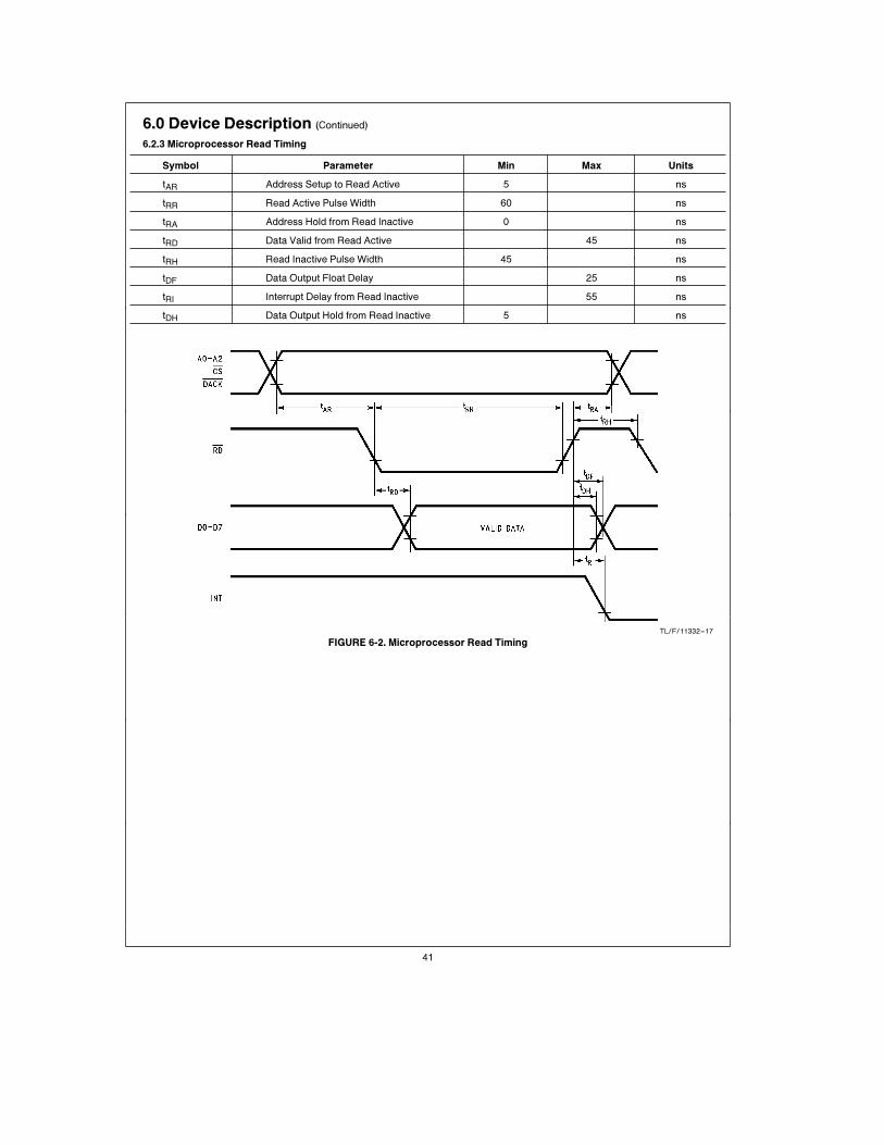
6.0 Device Description (Continued)
6.2.3 Microprocessor Read Timing
Symbol Parameter Min Max Units
tAR Address Setup to Read Active 5 ns
tRR Read Active Pulse Width 60 ns
tRA Address Hold from Read Inactive 0 ns
tRD Data Valid from Read Active 45 ns
tRH Read Inactive Pulse Width 45 ns
tDF Data Output Float Delay 25 ns
tRI Interrupt Delay from Read Inactive 55 ns
tDH Data Output Hold from Read Inactive 5 ns
TL/F/11332–17
FIGURE 6-2. Microprocessor Read Timing
41
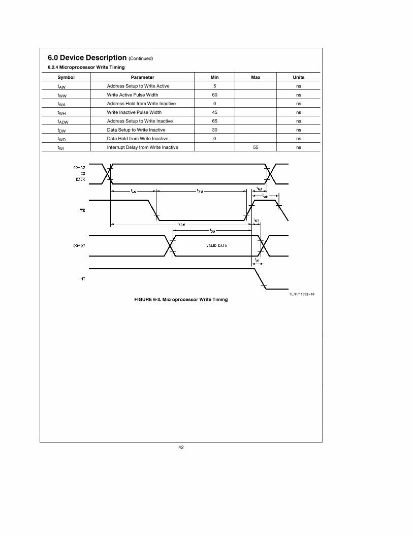
6.0 Device Description (Continued)
6.2.4 Microprocessor Write Timing
Symbol Parameter Min Max Units
tAW Address Setup to Write Active 5 ns
tWW Write Active Pulse Width 60 ns
tWA Address Hold from Write Inactive 0 ns
tWH Write Inactive Pulse Width 45 ns
tADW Address Setup to Write Inactive 65 ns
tDW Data Setup to Write Inactive 30 ns
tWD Data Hold from Write Inactive 0 ns
tWI Interrupt Delay from Write Inactive 55 ns
TL/F/11332–18
FIGURE 6-3. Microprocessor Write Timing
42

6.0 Device Description (Continued)
6.2.5 DMA Timing
Symbol Parameter Min Max Units
tQP DRQ Period (Except Non-Burst DMA) (Note 8) 8 x tDRP ms
tQQ DRQ Inactive Non-Burst Pulse Width 300 400 ns
tKQ DACK Active Edge to DRQ Inactive 65 ns
tRQ RD, WR Active Edge to DRQ Inactive (Note 7) 65 ns
tQR DRQ to RD, WR Active 15 ns
tTT TC Active Pulse Width 50 ns
tTQ TC Active Edge to DRQ Inactive (Note 9) 75 ns
tKK DACK Active Pulse Width 65 ns
tKI DACK Inactive Pulse Width 25 ns
tKR DACK Setup to RD, WR Active 5 ns
tRK DACK Hold from RD, WR Inactive 0 ns
tQW DRQ to End of RD, WR (Note 8) (8 x tDRP ms(DRQ Service Time) b16 x tICP)
tQT DRQ to TC Active (Note 8) (8 x tDRP ms(DRQ Service Time) b16 x tICP)
Note 7: The active edge of RD or WR is recognized only when DACK is active.
Note 8: Values shown are with the FIFO disabled, or with FIFO enabled and THRESH e 0. For nonzero values of THRESH, add (THRESH x 8 x tDRP) to the values
shown.
Note 9: During normal DMA operation TC should occur when DACK is active during the last byte of the last sector transferred.
TL/F/11332–19
FIGURE 6-4. DMA Timing
43

6.0 Device Description (Continued)
6.2.6 Reset Timing
Symbol Parameter Min Max Units
tRW Reset Width (Note 10) 100 ns
tRC Reset to Control Inactive 300 ns
Note 10: The software reset pulse width is 100 ns. The hardware reset pulse width with an external 10 kX pull-up or pull-down resistor on the MFM pin is 100 ns.
When using the internal pull-up resistor on the MFM pin, the hardware reset pulse width is 170 ns (assumes no load on MFM).
TL/F/11332–20
FIGURE 6-5. Reset Timing
6.2.7 Write Data Timing
Symbol Parameter Min Max Units
tWDW Write Data Pulse Width Table 6-2 ns
tHDS HDSEL Setup to WGATE Active 100 ms
tHDH HDSEL Hold from WGATE Inactive 750 ms
TABLE 6-2. Minimum tWDW Values
Data Rate tDRP tWDW tWDW Value Units
1 Mb/s 1000 2 x tICP 250 ns
500 kb/s 2000 2 x tICP 250 ns
300 kb/s 3333 2 x tICP 375 ns
250 kb/s 4000 2 x tICP 500 ns
TL/F/11332–21
FIGURE 6-6. Write Data Timing
44

6.0 Device Description (Continued)
6.2.8 Drive Control Timing
Symbol Parameter Min Max Units
tDRV DR0–DR3, MTR0–MTR3 from End of WR 100 ns
tDST DIR Setup to STEP Active 6 ms
tSTD DIR Hold from STEP Inactive tSRT ms
tSTP STEP Active High Pulse Width 8 ms
tSRT STEP Rate Time (see Table 4-13) 1 ms
tIW Index Pulse Width 100 ns
TL/F/11332–22
FIGURE 6-7. Drive Control Timing
6.2.9 Read Data Timing
Symbol Parameter Min Max Units
tRDW Read Data Pulse Width 50 ns
TL/F/11332–23
FIGURE 6-8. Read Data Timing
45

7.0 Reference Section7.1 MNEMONIC DEFINITIONS FOR PC8477B COMMANDS
Symbol Description
BFR Buffer enable bit used in the Mode command.
Enabled open-collector output buffers.
BST Burst Mode disable control bit used in Mode
command. Selects the Non-Burst FIFO mode if
the FIFO is enabled.
DC0 Drive Configuration 0–3. Used to set a drive to
conventional or perpendicular mode. Used inDC1
Perpendicular Mode command.DC2
DC3
DENSEL Density Select control bits used in the Mode
command.
DIR Direction control bit used in Relative Seek
command to indicate step in or out.
DMA DMA mode enable bit used in the Specify
command.
DR0 Drive Select 0–1 bits used in most commands.
Selects the logical drive.
DTL Data Length parameter used in the Read, Write,
Scan and Verify commands.
EC Enable Count control bit used in the Verify
command. When this bit is 1, the DTL parameter
becomes SC (Sector Count).
EIS Enable Implied Seeks. Used in the Configure
command.
EOT End of Track parameter set in the Read, Write,
Scan, and Verify commands.
ETR Extended Track Range used with the Seek
command.
FIFO First-In First-Out buffer. Also a control bit used in
the Configure command to enable or disable the
FIFO.
FRD FIFO Read disable control bit used in the Mode
command.
FWR FIFO Write disable control bit used in the Mode
command.
GAP Gap2 control bit used in the Perpendicular Mode
command.
HD Head Select control bit used in most commands.
Selects Head 0 or 1 of the disk.
IAF Index Address Field control bit used in the Mode
command. Enables the ISO Format during the
Format command.
IPS Implied Seek enable bit used in the Mode, Read,
Write, and Scan commands.
LOCK Lock enable bit in the Lock command. Used to
make certain parameters unaffected by a
software reset.
LOW Low Power control bits used in the Mode
command.PWR
Symbol Description
MFM Modified Frequency Modulation control bit used
in the Read, Write, Format, Scan and Verify
commands. Selects MFM or FM data encoding.
MFT Motor Off Time programmed in the Specify
command.
MNT Motor On Time programmed in the Specify
command.
MT Multi-Track enable bit used in the Read, Write,
Scan and Verify commands.
OW Overwrite control bit used in the Perpendicular
Mode command.
POLL Enable Drive Polling bit used in the Configure
command.
PRETRK Precompensation Track Number used in the
Configure command.
PTR Present Track Register. Contains the internal
track number for one of the four logical disk
drives.
PU Pump diagnostic enable bit used in the Mode
command.
R255 Recalibrate control bit used in Mode command.
Sets maximum recalibrate step pulses to 255.
RG Read Gate diagnostic enable bit used in the
Mode command.
RTN Relative Track Number used in the Relative
Seek command.
SC Sector Count control bit used in the Verify
command.
SK Skip control bit used in read and scan
operations.
SRT Step Rate Time programmed in the Specify
command. Determines the time between step
pulses for seek and recalibrates.
ST0 Status Register 0–3. Contains status
information about the execution of a command.ST1
Read in the Result Phase of some commands.ST2
ST3
THRESH FIFO threshold parameter used in the Configure
command.
TMR Timer control bit used in the Mode command.
Affects the timers set in the Specify command.
WG Write Gate control bit used in the Perpendicular
Mode command.
WLD Wildcard bit in the Mode command used to
enable or disable the wildcard byte (FF) during
Scan commands.
46
7.0 Reference Section (Continued)
7.2 PC8477B ENHANCEMENTS VS 82077AA
The enhancements listed below are additional functions of
the PC8477B that the 82077AA does not have, and do not
affect the compatibility between the two floppy controllers.
Commands
The following are PC8477B commands not supported by
the 82077AA.
Mode CommandÐControls several enhanced fea-
tures of the PC8477B such as: Implied Seeks, Low
Power mode, additional FIFO modes, and DENSEL
encoding. The Mode command parameters are de-
fault to 82077AA compatible states, and will be un-
affected by 82077AA-based software that does not
recognize the existence of a Mode command. See
the PC8477B data sheet for more details.
NSC CommandÐThis one byte command is used
to identify the PC8477B in the system. Other floppy
controllers will return an 80 hex (invalid command),
while the PC8477B will return a value of 73 hex (the
lower four bits are reserved to indicate revision up-
dates in the part).
Set Track CommandÐThis command allows the
user to program the value of any of the four Present
Track Registers corresponding to the four logical
drives.
FIFO Operation
The PC8477B FIFO is compatible with the 82077AA FIFO,
with the addition of a Non-Burst mode. The default setting
when the FIFO is enabled is the 82077AA compatible Burst
mode. The Non-Burst mode is enabled via the Mode com-
mand. The Non-Burst mode will pulse the DRQ or INT sig-
nals during a burst transfer to or from the FIFO.
For both the Burst and Non-Burst modes with the FIFO en-
abled, no external circuitry is required with the PC8477B
during DMA verify transfers. During verify operations, the
DMA controller will assert the DACK signal without a RD
signal in response to a DRQ from the floppy controller. The
82077AA, however, requires external circuitry to create the
RD signal during DMA verify operations with its FIFO en-
abled in order to work successfully without an overrun error.
The published Intel bug fix for the 82077AA can only be
used for motherboard applications and not for add-in
boards. The PC8477B does not have this problem.
Also, because of the byte counter in the PC8477B design,
the DRQ or INT signal will be deasserted when the last byte
of a sector is written to the FIFO during the execution phase
of a write or format operation. The 82077AA does not deas-
sert DRQ or INT until the last byte has been read out of the
FIFO. This will cause a delay in the deassertion of DRQ or
INT of up to 16 byte times, resulting in extra bytes trans-
ferred to the floppy controller. The PC8477B does not have
this problem.
Data Separator
The PC8477B data separator’s performance meets that of
the 82077AA’s. However, there are no dual modes in the
PC8477B data separator whereas the 82077AA data sepa-
rator has an internal floppy drive mode and an internal tape
drive mode. This singular mode design of the PC8477B data
separator eliminates the need for hardware or software con-
trol and provides for more consistent performance. The
PC8477B data separator is designed to work with the strict-
est motor speed and bit jitter requirements of both floppy
and tape drives.
Low Power Mode
The typical measured low power current for the PC8477B
(analog and digital) is 1 mA. The typical measured low pow-
er current for the 82077AA is 2 mA–3 mA.
The PC8477A supports the 82077AA manual low power
mode by writing to the Low Power bit (D6) in the Data Rate
Select register. The low power mode is turned off by issuing
a reset to the chip, whereupon re-initialization is necessary.
In addition, the PC8477B supports a manual low power AND
automatic low power mode via the Mode command. Manual
low power must be invoked every time the low power mode
is desired. Automatic low power mode need only be invoked
once during initialization, and then low power is entered
whenever the floppy controller is idle.
As mentioned, the 82077AA and PC8477B will exit the low
power mode after a reset. The PC8477B will also exit the
low power mode after any read or write to the Main Status
Register or Data Register. In this way, the part can exit low
power cleanly without requiring additional software initializa-
tion. This feature gives the PC8477B an advantage in that
once software has initialized it for automatic low power, no
additional software modifications are necessary, and the
chip will power down whenever it is idle. Even for manual
low power mode via the DSR or Mode command, the
PC8477B can return to normal mode without re-initialization,
as required for the 82077.
Reset Pulse Width
The PC8477B software reset pulse width is 100 ns mini-
mum. This means that software can issue two consecutive
writes to the Digital Output Register of the PC8477B to tog-
gle the Reset Controller bit (D2) without intervening delay.
This specification is significantly better than the 82077AA
minimum software reset pulse width, which is specified as
3.5 ms (worst case at the 250 kb/s data rate).
When using an external pull-up or pull-down 10 kX resistor
on the MFM pin, the hardware reset pulse width is also
100 ns minimum for the PC8477B. The minimum hardware
reset pulse width for the 82077AA is 7.1 ms. Again, the
PC8477B specification is much better, allowing the system
reset pulse to be very short.
Tape Drive Register
The PC8477B will support reads and writes to this register,
just as the 82077AA does. However, the PC8477B will not
use the information written to the Tape Drive Register to
alter the state of the Data Separator. That is, there is only
one mode of the internal PC8477B data separator, a high
performance mode that will support the requirements for all
floppy and tape drives.
Implied Seeks
The PC8477B supports our popular DP8473 method as well
as the 82077AA method of implementing Implied Seeks.
The DP8473 method is to set a bit in the Mode command
for enabling Implied Seeks, and then set the Implied Seek
bit if desired in the Read, Write, or Scan commands. The
82077AA method is to set the EIS bit (enable implied seeks)
in the Configure command, and then Implied Seeks will al-
ways be enabled for Read, Write, and Verify commands.
47

7.0 Reference Section (Continued)
TABLE 7-1 8477B–82077 Parameter Comparison
Description PC8477B 82077AA 82077SL Units
Absolute Maximum Ratings
Supply Voltage b0.5–7.0 b0.5–8.0 b0.5–8.0 V
DC Limits
VIH Clock MIN 2.0 3.9 3.9 V
IOL MFM pin (VOL e 0.4V) 4.0 2.5 2.5 mA
IOH MFM pin (VOH e 3.0V) b4.0 b2.5 b2.5 mA
ICC Low Power (Analog a Digital) Typical 0.505 1.5 Ð mA
ICCLow Power (Analog a Digital) Tested 2.05 no spec Ð mA
AC Timings
t5 (tICP)–INTERNAL Clock Period
1 Mb/s 125 125 125 ns
500 kb/s 125 250 250 ns
300 kb/s 208 420 420 ns
250 kb/s 250 500 500 ns
t8 (tRR)–Read Active Pulse Width MIN 60 90 90 ns
t10 (tRD)–Read to Valid Data 45 80 80 ns
t11 (tRH)–Read Inactive Pulse Width 45 60 60 ns
t12 (tDF)–Delay to Float 25 35 35 ns
t13 (tRI)–Interrupt Delay from Read Inactive MAX
1 Mb/s 55 250 250 ns
500 kb/s 55 375 375 ns
300 kb/s 55 545 545 ns
250 kb/s 55 625 625 ns
t16 (tWW)–Write Active Pulse Width MIN 60 90 90 ns
t19 (tDW)–Data Setup to Write Active 30 70 70 ns
t18 (tWH)–Write Inactive Pulse Width 45 60 60 ns
tADW–Address Setup to Write Inactive MIN 65 no spec no spec ns
t21 (tWI)–Interrupt Delay from Write Inactive
1 Mb/s 55 250 250 ns
500 kb/s 55 375 375 ns
300 kb/s 55 545 545 ns
250 kb/s 55 625 625 ns
t22 (tQP)–DRQ Cycle Period MIN 8 6.5 6.5 ms
t23 (tKQ)–DACK Active to DRQ Inactive MAX 65 75 75 ns
t23a (tQK a tKK)–DRQ to DACK Inactive
1 Mb/s 60 no spec 83 ns
500 kb/s 60 no spec 166 ns
300 kb/s 60 no spec 280 ns
250 kb/s 60 no spec 333 ns
t24 (tRQ)–RD, WR Active to DRQ Inactive MAX 65 100 100 ns
t27 (tQR)–DRQ to RD, WR Active MIN 15 0 0 ns
t29 (tTQ)–TC Active to DRQ Inactive MAX 75 150 150 ns
tKK–DACK Active Pulse Width MIN 65 no spec no spec ns
tKI–DACK Inactive Pulse Width MIN 25 no spec no spec ns
tQK–DRQ to DACK Active MIN 10 no spec no spec ns
t30 (tRW)–Reset Pulse Width MIN 100 7083 7083 ns
t30a (tRW)–Software Reset Pulse Width MIN (Worst Case) 100 3500 500 ns
t31 (tRC)–Reset to Control Inactive 160 2000 2000 ns
t32 (tWDW)–Write Data Pulse Width MIN
1 Mb/s 250 150 150 ns
500 kb/s 250 360 360 ns
300 kb/s 416 615 615 ns
250 kb/s 500 740 740 ns
48

7.0 Reference Section (Continued)
TABLE 7-1 8477B–82077AA Parameter Comparison (Continued)
Description PC8477B 82077AA 82077SL Units
AC Timings (Continued)
t35 (tDST)–DIR Setup to STEP Active MIN 6 4 4 ms
t36 (tSTD)–DIR Hold from STEP Inactive MIN tSRT 10 10 ms
t37 (tSTP)–STEP Active Pulse Width 8 2.5 2.5 ms
t39 (tIW)–Index Pulse Widh MIN
1 Mb/s 100 625 625 ns
500 kb/s 100 1250 1250 ns
300 kb/s 100 2100 2100 ns
250 kb/s 100 2500 2500 ns
t41 (tHDH)–HDSEL Hold from WGATE Inactive MIN
1 Mb/s *750 716 716 ms
500 kb/s *750 1432 1432 ms
300 kb/s *750 2719 2719 ms
250 kb/s *750 2864 2864 ms
tHDS–HDSEL Setup to WGATE Active *100 no spec no spec ms
*These timings are required to support perpendicular recording drives.
49
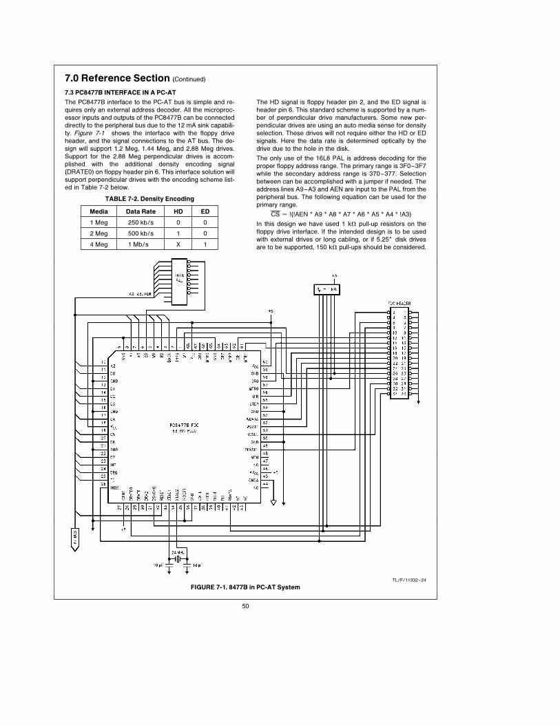
7.0 Reference Section (Continued)
7.3 PC8477B INTERFACE IN A PC-AT
The PC8477B interface to the PC-AT bus is simple and re-
quires only an external address decoder. All the microproc-
essor inputs and outputs of the PC8477B can be connected
directly to the peripheral bus due to the 12 mA sink capabili-
ty. Figure 7-1 shows the interface with the floppy drive
header, and the signal connections to the AT bus. The de-
sign will support 1.2 Meg, 1.44 Meg, and 2.88 Meg drives.
Support for the 2.88 Meg perpendicular drives is accom-
plished with the additional density encoding signal
(DRATE0) on floppy header pin 6. This interface solution will
support perpendicular drives with the encoding scheme list-
ed in Table 7-2 below.
TABLE 7-2. Density Encoding
Media Data Rate HD ED
1 Meg 250 kb/s 0 0
2 Meg 500 kb/s 1 0
4 Meg 1 Mb/s X 1
The HD signal is floppy header pin 2, and the ED signal is
header pin 6. This standard scheme is supported by a num-
ber of perpendicular drive manufacturers. Some new per-
pendicular drives are using an auto media sense for density
selection. These drives will not require either the HD or ED
signals. Here the data rate is determined optically by the
drive due to the hole in the disk.
The only use of the 16L8 PAL is address decoding for the
proper floppy address range. The primary range is 3F0–3F7
while the secondary address range is 370–377. Selection
between can be accomplished with a jumper if needed. The
address lines A9–A3 and AEN are input to the PAL from the
peripheral bus. The following equation can be used for the
primary range.
CS e !(!AEN * A9 * A8 * A7 * A6 * A5 * A4 * !A3)
In this design we have used 1 kX pull-up resistors on the
floppy drive interface. If the intended design is to be used
with external drives or long cabling, or if 5.25× disk drives
are to be supported, 150 kX pull-ups should be considered.
TL/F/11332–24
FIGURE 7-1. 8477B in PC-AT System
50

7.0 Reference Section (Continued)
7.4 SOFTWARE INITIALIZATION SEQUENCE
Following power up the system will issue a hardware reset
to the PC8477B. This will put the internal registers and cir-
cuitry into a known state after which the software initializa-
tion sequence can begin.
End ResetÐThe first task is to bring the PC8477B out of
the reset state by writing 0CH to the DOR register. The
software should then poll the MSR until 80H is returned. At
this point the controller is ready to begin processing com-
mands.
Service Ready Changed State InterruptÐOnce an inter-
rupt is received the software should issue 4 SENSE INTER-
RUPT commands for each of the 4 logical drives. This is
due to the fact that after a reset, drive polling is enabled by
default.
Set Data RateÐThe data rate should be set via a write to
the CCR register. The default state is 250 kb/s following
reset.
Configure the FIFOÐThe default setting is with the FIFO
disabled. If the perpendicular format is to be supported the
FIFO will need to be enabled due to the higher data rates
used. The FIFO threshold level should be set based on the
DMA response time of the system. A lower value of
THRESH corresponds to a fast system with a quick DMA
response time, whereas a higher value of THRESH corre-
sponds to a sluggish system with slower DMA response
time. A write to the configuration register is also used to
enable implied seeks if that feature is desired.
LockÐThis command will lock the FIFO parameters which
will leave them unaffected following a reset. Set the LOCK
bit to 1 to lock the parameters.
Specify CommandÐAfter a reset a specify command must
always be issued in the initialization sequence. This is be-
cause there is no default for these values. With this com-
mand you will set up the motor on and motor off times as
well as the step rate times. DMA mode is also enabled via
this command.
Mode CommandÐThere are several advanced features
that can be enabled via the mode command. Head settling
time for implied seeks, open collector drive interface out-
puts, ISO format pattern, low power modes, enabling 255
step pulses for higher density media, and FIFO burst mode
are just some of the features.
Recalibrate DriveÐFirst access to the drive should be to
RECALIBRATE to track 0. Following the recalibrate com-
mand it is necessary to issue a SENSE INTERRUPT com-
mand to determine if the recalibrate was successful. If no
track 0 was detected, an error will be reported. This is a
common method to determine if a drive is connected.
Seek/Read/Write/FormatÐAt this point the initialization
is complete and normal disk I/O operations would start to
occur. In normal operations it would not be necessary to re-
initialize prior to each access. Normal disk I/O operations
would include writes to CCR register to change data rates,
recalibrating to track 0, toggling the motor and drive selects
through the DOR register, seeking to the appropriate track,
and initializing the DMA controller prior to Read/Write/For-
mat commands.
Figure 7-2 shows a block diagram representing the initializa-
tion sequence for the PC8477B.
TL/F/11332–25
FIGURE 7-2. PC8477B Initialization
7.5 PC8477A/PC8477B DIFFERENCES
There are two differences to note between the 8477A and
8477B versions. The NSC command result phase returns a
73H in the 8477B, and returns a 72H in the 8477A. This
command is used strictly to distinguish new revisions of the
part. The second difference pertains to the Motor On Time
(MNT) values when the FDC is in Mode 1. The new table is
listed in Table 4-15 of this document. The MNT values at
500 kb/s for Mode 1 were changed to be the same as the
1 Mb/s values. The changes to the MNT values should not
affect application software.
7.6 REVISION HISTORY
Nov. 1990 Preliminary PC8477 datasheet
May 1992 Preliminary PC8477B datasheet
ÐAdd new part markings
ÐAdd PQFP package option
ÐAdd 1.25 Mb/s data rate support
ÐAdd Dynamic Window Margin spec.
ÐImprove ICC and AC databus timings
ÐAdd applications reference section
June 1993 Final PC8477B datasheet
ÐElimination of 1.25 Mb/s data rate support
ÐElimination of FM mode functional testing
ÐESD tolerance spec. raised to 2000V
ÐReplace tQK spec. with tKR and tRKÐChange tRC spec. from 160 ns to 300 ns
ÐChange tWDW @300 Kb/s from 416 ns to 375 ns
51

52

Physical Dimensions inches (millimeters)
Plastic Chip Carrier (V)
Order Number PC8477BV-1
NS Package Number VA68A
53

PC
8477B
(SuperF
DC
)A
dvanced
Flo
ppy
Dis
kC
ontr
oller
Physical Dimensions inches (millimeters) (Continued)
Plastic Quad Flat Package (PQFP)
Order Number PC8477BVF-1
NS Package Number VF60A
LIFE SUPPORT POLICY
NATIONAL’S PRODUCTS ARE NOT AUTHORIZED FOR USE AS CRITICAL COMPONENTS IN LIFE SUPPORT
DEVICES OR SYSTEMS WITHOUT THE EXPRESS WRITTEN APPROVAL OF THE PRESIDENT OF NATIONAL
SEMICONDUCTOR CORPORATION. As used herein:
1. Life support devices or systems are devices or 2. A critical component is any component of a life
systems which, (a) are intended for surgical implant support device or system whose failure to perform can
into the body, or (b) support or sustain life, and whose be reasonably expected to cause the failure of the life
failure to perform, when properly used in accordance support device or system, or to affect its safety or
with instructions for use provided in the labeling, can effectiveness.
be reasonably expected to result in a significant injury
to the user.
National Semiconductor National Semiconductor National Semiconductor National Semiconductor National Semiconductores National SemiconductorCorporation GmbH Japan Ltd. Hong Kong Ltd. Do Brazil Ltda. (Australia) Pty, Ltd.2900 Semiconductor Drive Livry-Gargan-Str. 10 Sumitomo Chemical 13th Floor, Straight Block, Rue Deputado Lacorda Franco Building 16P.O. Box 58090 D-82256 F 4urstenfeldbruck Engineering Center Ocean Centre, 5 Canton Rd. 120-3A Business Park DriveSanta Clara, CA 95052-8090 Germany Bldg. 7F Tsimshatsui, Kowloon Sao Paulo-SP Monash Business ParkTel: 1(800) 272-9959 Tel: (81-41) 35-0 1-7-1, Nakase, Mihama-Ku Hong Kong Brazil 05418-000 Nottinghill, MelbourneTWX: (910) 339-9240 Telex: 527649 Chiba-City, Tel: (852) 2737-1600 Tel: (55-11) 212-5066 Victoria 3168 Australia
Fax: (81-41) 35-1 Ciba Prefecture 261 Fax: (852) 2736-9960 Telex: 391-1131931 NSBR BR Tel: (3) 558-9999Tel: (043) 299-2300 Fax: (55-11) 212-1181 Fax: (3) 558-9998Fax: (043) 299-2500
National does not assume any responsibility for use of any circuitry described, no circuit patent licenses are implied and National reserves the right at any time without notice to change said circuitry and specifications.