tutorial on direct digital synthesizer structure
TRANSCRIPT

TUTORIAL ON DIRECT DIGITAL SYNTHESIZER STRUCTURE IMPROVEMENTS AND
STATIC TIMING ANALYSIS
BY
ZEXIAN LI
THESIS
Submitted in partial fulfillment of the requirements
for the degree of Master of Science in Electrical and Computer Engineering
in the Graduate College of the
University of Illinois at Urbana-Champaign, 2018
Urbana, Illinois
Adviser:
Professor Jose E. Schutt-Aine

ii
ABSTRACT
The direct digital frequency synthesizer (DDS) has been widely used in digital communication
systems due to its high frequency resolution, fast frequency conversion, and continuous phase
change. With the development of microelectronics technology, field-programmable gate array
(FPGA) devices have been rapidly developed. Because of FPGAs’ high speed, high integration
and field-programmable advantages, the devices are widely used in digital processing and are
increasingly favored by hardware circuit design engineers. FPGAs also provide a technique for
using digital data processing blocks as a means to generate a frequency and phase tunable output
signal referenced to a fixed-frequency precision clock source. Many telecommunication
applications require such high-speed switching, fine tunability and superior quality signal source
for their components. This thesis will introduce the direct digital synthesizer (DDS) and investigate
some ways to optimize the DDS structure to save hardware resources and increase chip speed
without sacrificing signal quality.
The Verilog hardware description language is used as the development language. This thesis will
describe entire designs of both DDS with traditional structure and DDS with new structures. By
comparing the outputs, it also examines the corresponding simulation results and verifies the
improvement of the signal quality.

iii
To my family, for their love, support, motivation and patience.
To my adviser, for his support, guidance and advice.
To my student coworkers, for their advice and help.

iv
ACKNOWLEDGMENTS
I would like to thank my graduate school adviser, Professor Jose E. Schutt-Aine, for all his kind
help, support, encouragement and guidance along the way. He is a very kind and knowledgeable
professor who is always willing to help the students when they are in need. I have greatly benefited
from Professor Schutt-Aine’s profound knowledge, rigorous academic attitude, practical work
style and spirit of seeking truth and knowledge. I feel very blessed that I have had the opportunity
to learn from and work with my brilliant adviser and his research group in these past years. And
thanks to the visiting scholar Lan Chen who helped me during her visiting time and gave me some
perspectives I had not thought of before.
Also, I would like to give my special thanks to my good friends and colleagues: Xinying Wang,
Xu Chen, Xiao Ma, Nancy Zhao, Ashwarya Rajwardan, Bobi Shi, Thong Nguyen, Pin-Chiao
Huang and Bohao Wu for the invaluable discussions, all the late nights and indelible memories we
have together.
Last but not least, I would like to give my sincere thanks to my parents for all their support,
patience, understanding and love.

v
TABLE OF CONTENTS
CHAPTER 1: INTRODUCTION.................................................................................................. 1
1.1 Purpose and Motivation…............................................................................................1
1.2 Outline ..........................................................................................................................3
CHAPTER 2: TRADITIONAL AND NEW STRUCTURE DDS FUNDAMENTALS................4
2.1 Basic Working Principle of Traditional DDS................................................................4
2.2 Basic Working Principle of New Structure of DDS......................................................9
CHAPTER 3: FPGA DESIGN FLOW AND DESCRIPTION.......................................................15
CHAPTER 4: DDS FPGA DESIGN AND SIMULATION RESULTS........................................19
CHAPTER 5: DDS TIMING REPORTS AND STATIC TIMING ANALYSIS TUTORIAL....24
5.1 Static Timing Analysis.................................................................................................24
5.2 Static Timing Analysis for FPGA.................................................................................24
5.3 Factors Limiting the Maximum Frequency of the FPGA.............................................25
5.4 TimeQuest Basic Process.............................................................................................26
CHAPTER 6: SPURS IN THE DDS…..........................................................................................33
CHAPTER 7: CONCLUSION AND FUTURE WORK............................................................... 37
REFERENCES ..............................................................................................................................38

1
CHAPTER 1: INTRODUCTION
1.1 Purpose and Motivation
The direct digital synthesizer (DDS) is a popular technique for frequency synthesis. The main idea
of DDS is using digital data processing blocks as a means to generate a frequency- and phase-
tunable output signal referenced to a fixed-frequency precision clock source. Today’s cost-
competitive, high-performance, functionally integrated, and small package-sized DDS products
are fast becoming an alternative to traditional frequency-agile analog synthesizer solutions [1].
The topology of a conventional direct digital synthesizer (DDS) is shown in Figure 1.1 which
consists of five primary elements: a driving clock, a phase accumulator (PA), a look-up table
(LUT), a digital-to-analog converter (DAC), and a reconstruction filter [2]. It was presented by
Tierney, Rader and Gold in 1971 [3]. The traditional DDS will be explained and discussed in more
detail in Chapter 2. [2]
Figure 1.1: Basic structure of a generic direct digital synthesizer
The PLL offers very good wide tuning bandwidth due to the use of a programmable divider as
compared to DDFS approach [4]. On the other hand, DDFS provides many significant advantages
such as fast settling time, sub-hertz frequency resolution, continuous-phase switching response

2
and low phase noise [5], [6]. Compared with other frequency synthesizing techniques such as
VCO, DDS gives much higher frequency resolution, faster frequency channel switching with
continuous phase, wider range of frequency tuning and more flexible and versatile modulation
capability [7]. Nowadays, the cost-competitive, high-performance, functionality-integrated and
small-package DDS products are widely used in the field of telecommunications and are becoming
an alternative to some traditional analog synthesizer solutions. The applications of DDS include
signal generation, local oscillators, function generators, mixers, modulators, and sound
synthesizers. The advantages of DDS are the following: (1) DDS has micro-hertz tuning resolution
of the output frequency and sub-degree phase tuning capability, all under complete digital control.
(2) DDS has extremely fast “hopping speed” in tuning output frequency (or phase), phase-
continuous frequency hops with no over/undershoot or analog-related loop settling time anomalies.
(3) The DDS digital architecture eliminates the need for the manual system tuning and tweaking
associated with component aging and temperature drift in analog synthesizer solutions. (4) The
digital control interface of the DDS architecture facilitates an environment where systems can be
remotely controlled, and minutely optimized, under processor control. (5) When utilized as a
quadrature synthesizer, DDS affords unparalleled matching and control of I and Q synthesized
outputs [8].
This thesis uses an optimized design of DDS to minimize hardware complexity, reduce chip area
and power consumption, and increase chip speed while maintaining the original advantages of
DDS. The DDS will be designed and implemented in Verilog codes that are synthesizable on an
FPGA. FPGA is widely used in digital circuit design for its flexibility, accuracy and effectiveness.

3
The most significant advantage of using an FPGA is that designs can be created and changed in a
very short period. Instead, with application-specific integrated circuits (ASICs), the designers will
have to wait months for the circuits to be fabricated.
1.2 Outline
This thesis will serve as a complete tutorial on the background knowledge of DDS with the
traditional structure and DDS with the new structure to save resources without sacrificing the
performance.
● Chapter 2 provides an overview of the theory and structure of the DDS with both traditional
and new structure.
● Chapter 3 introduces the background knowledge of FPGA and the FPGA design flow.
● Chapter 4 presents the implementation and simulation difference between traditional DDS
and DDS with new structure on FPGA in Altera Quartus FPGA development software.
● Chapter 5 presents the simulation results from the different structures of DDS and some
theoretical analysis of the results. This chapter will focus on the optimized design of DDS
which is to minimize hardware complexity, reduce chip area and power consumption, and
increase chip speed while maintaining the original advantages of DDS.
● Chapter 6 concludes this thesis with a summary and potential research topics and
improvements.
4
CHAPTER 2: TRADITIONAL AND NEW STRUCTURE DDS FUNDAMENTALS
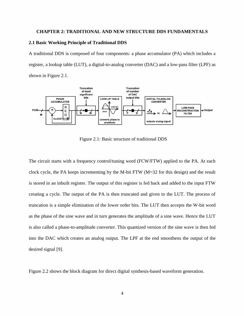
2.1 Basic Working Principle of Traditional DDS
A traditional DDS is composed of four components: a phase accumulator (PA) which includes a
register, a lookup table (LUT), a digital-to-analog converter (DAC) and a low-pass filter (LPF) as
shown in Figure 2.1.
Figure 2.1: Basic structure of traditional DDS
The circuit starts with a frequency control/tuning word (FCW/FTW) applied to the PA. At each
clock cycle, the PA keeps incrementing by the M-bit FTW (M=32 for this design) and the result
is stored in an inbuilt register. The output of this register is fed back and added to the input FTW
creating a cycle. The output of the PA is then truncated and given to the LUT. The process of
truncation is a simple elimination of the lower order bits. The LUT then accepts the W-bit word
as the phase of the sine wave and in turn generates the amplitude of a sine wave. Hence the LUT
is also called a phase-to-amplitude converter. This quantized version of the sine wave is then fed
into the DAC which creates an analog output. The LPF at the end smoothens the output of the
desired signal [9].
Figure 2.2 shows the block diagram for direct digital synthesis-based waveform generation.

5
Figure 2.2: Direct digital synthesis block diagram
Phase Accumulator (PA): The PA is principally a combination of an adder, a counter and a register.
At each clock cycle the M-bit word of the PA increments by the FTW, thereby producing a
quantized saw-tooth waveform as in Figure 2.3 [2]. Each dot on the saw-tooth waveform is the
value that comes out of the register.
Figure 2.3: Saw-tooth output of phase accumulator
Now since we give an input of an M-bit word, the PA has 2^M possible values. The final frequency
of the sine wave is directly dependent on the frequency of this saw-tooth waveform produced at

6
the PA. Thus, the larger the M word, the faster the PA jumps, which leads to a higher frequency
at the output. From the output of the PA we could derive the ultimate frequency of the sine wave
as in Equation 2.1:
fout = FTW/2M * fclk (2.1)
And because DDS follows Nyquist’s sampling law, the highest output frequency is half the clock
frequency. In practice, the highest output frequency of the DDS is determined by the spur level of
the allowable output, which is generally fo ≤ 40% fc.
As Figure 2.2 illustrates, a phase accumulator compares the sample clock and desired frequency
to increment a phase register. Again, the fundamental idea is that we can generate signals with
precise frequencies by generating an appropriate sample based on the phase of that frequency at
any point in time. In addition, by representing our waveform with 214 (16,384) points, we are able
to represent exactly 16,384 phase increments with our lookup table. The phase accumulator uses
simple arithmetic operations to calculate the lookup table address for each generated sample. It
does this by dividing the desired frequency by the sample clock and multiplying the result by 248.
This number is based on the bit resolution of the phase register. For NI signal generators, a 48-bit
phase register is used for maximum precision. Of these, 34 bits are used to store the remainder
phase, and 14 bits are used to choose a sample from the lookup table.
Thus, the phase accumulator produces a 14-bit address that corresponds to the exact phase of the
signal. For example, an address of ‘00000000000000’ corresponds to 0°. On the other hand, an
address of ‘11111111111111’ corresponds to 359.978°. Thus, the signal generator can use this
address to control the phase of the signal at any point in time. This process is shown in Figure 2.4.

7
Figure 2.4: Computation of the phase register
As Figure 2.4 suggests, the phase accumulator is able to represent the phase of the generated signal
with 248 points of precision. However, because we only have 214 available points in our waveform,
only the 14 most significant bits of the phase register are used in the lookup table. The remaining
34 bits are used to store the remainder of the phase increment. This remainder enables the DDS
precision by ensuring that the lookup table will return the appropriate phase information after the
phase register rolls over (once per period of the waveform) [8].
Lookup Table (LUT): The LUT behaves as a phase-to-amplitude conversion unit, thereby giving
us a discrete sine wave at the output. To keep the LUT reasonably sized we truncate the bits from
the PA and feed the higher order bits to the LUT [10]. For our design we choose bits 29 through
18 as the 12 bit W-word. This allows the hardware to be reasonably sized and not extremely power
hungry. The LUT will contain unique values of a sine wave over one period; however even in that
one period, the sine wave is symmetrical. To further exploit this symmetrical nature, we can fill
the table with values that correspond to only a quarter of a sine wave period [10].

8
For the FPGA design, one will need a coefficients file containing the values of the LUT. Generate
this file with the help of Matlab and store it as a ‘*.coe’. This file will then be added to the ROM.
Digital-to-Analog Converter (DAC): A second truncation process is carried out here, as the output
of the LUT is truncated to the appropriate number of bits and then given to the DAC. The DAC
creates an analog waveform from the discretized sine wave. An important fact to note here is that
the DAC is solely responsible for limiting the design’s maximum attainable frequency. It does not
matter how fast the PA is clocked as the DAC (which is one of two analog components in the
entire design) forms the bottleneck.
Low-Pass Filter (LPF): The LPF behaves as a reconstruction filter that smoothens the signal from
the DAC. Since we do not want any aliases of the fundamental frequency, this LPF also behaves
as an antialiasing filter [3], thereby limiting us to the Nyquist frequency. Typically, a Chebyshev
filter is used to build this stage due to its sharp frequency response characteristics [3].
In summary, the traditional DDS structure can be simplified as shown in Figure 2.5.
Figure 2.5: Traditional DDS structure block diagram
And the traditional DDS structure Quartus generated block diagram is as shown in Figure 2.6.

9
Figure 2.6: Traditional DDS Quartus generated block diagram
2.2 Basic Working Principle of New Structure of DDS
Similar to the traditional DDS structure, the new structure DDS block diagram is in Figure 2.7.
Figure 2.7: New structure DDS block diagram
The new DDS’s address converter is based on the value of the 2nd most significant address bit to
determine whether the value is increasing from cycle 0 to π / 2 or decreasing from cycle π / 2 to π,
while the data converter is based on the most significant address bit to determine whether the first
half of the generated waveform is from cycle 0 to π or the second half-cycle from π to 2π.

10
Based on the above theory, the sine address change converter block module is shown below in
Figure 2.8:
Figure 2.8: Sine address change module codes
And the data change converter block Verilog code is provided in Figure 2.9.
Figure 2.9 Data change module codes
The new DDS structure employs four pipelines. The 32-bit accumulator is divided into four
pipelines, each pipeline completing the 8-bit addition operation, and the pipeline’s carry is
cascaded. The pipeline structure can improve the accumulator operation speed by more than three
times. In order to improve the operation speed, the adder uses the fastest carry-lookahead bit
algorithm. The pipeline structure can improve the operation speed of the device. However, the

11
disadvantage is that the data needs to be kept for four clock cycles, which reduces the frequency
of the system hopping. The main codes of the four carry-forward adders are shown in Figure 2.10
and Figure 2.11. And the block diagram for the four-pipelining structure is shown in Figure 2.12.
Figure 2.10: Four carry-lookahead adders codes partI
Figure 2.11: Four carry-lookahead adders codes partII

12
Figure 2.12: Four pipeline structure block diagram
And after simulation, Figure 2.13 and 2.14 below show that with the new pipeline structure, the
maximum operating frequency rises from 284.82 MHz to 307.22 MHz, which is consistent with
the goal of the design. And the maximum allowed frequency (Fmax) can be found under the
TimeQuest Timing Analyzer -> Fmax Summary. The TimeQuest Timing Analyzer is used for
timing analysis in Quartus II which will be explained in more detail in Chapter 5.
Figure 2.13: Maximum operating frequency of traditional DDS
Figure 2.14: Maximum operating frequency of new structure DDS

13
For the compression of the ROM table, the second highest bit of the phase accumulator is used to
determine the quadrant, and the sinusoidal composite wave is synthesized into the range of 0 to π;
the highest bit is used as the sign bit, and the sine wave is synthesized into the range of 0 to 2π.
For a cosine wave, the sign bit is obtained by XORing the highest bit and the next highest bit
because the cosine waveform is π/2 phase ahead of the sinusoidal waveform. But since the sine
function and the cosine function are symmetric about π/4, it is possible to store only the sine and
cosine function values of (0 to π/4), so that the memory size will be reduced by half. The second
highest bit of the phase accumulator can be selected between 0 to π/4 and π/4 to π/2. When the
actual circuit is implemented, the next high bit is XORed with the next highest bit to generate this
signal. In addition, in order to complete the quadrature output, two 2:1 multiplexer circuits are
added.
Last but not the least, the last block change is the amplitude change module which saves more
resources to select to output the corresponding amplitude. The Verilog code for the amplitude
change module is provided in Figure 2.15.
Figure 2.15: Amplitude change module codes

14
The new DDS structure Quartus generated block diagram is shown in Figure 2.16.
Figure 2.16: New structure DDS Quartus generated block diagram
Figure 2.17: New structure DDS signals waveform
Figure 2.17 shows the intermediate signals in the new structure DDS design implementation.
Based on these new improvements analysis, the new DDS’s resource usages should be saved as
compared to the traditional DDS structure. More simulation results and comparisons will be shown
in the later chapters.

15
CHAPTER 3: FPGA DESIGN FLOW AND DESCRIPTION
There are two typical ways to design and implement digital circuits: application-specific
integrated circuits (ASIC) implementation and field-programmable gate array (FPGA)
implementation. The main difference between the two is that in the case of the FPGAs one can
program a ready development board and thus implement and test the design setup more quickly.
ASICs, however, are capable of a complete custom design, which makes them cheaper and smaller
since the device only contains components that are absolutely necessary to run the application.
More comparisons are listed in Figure 3.1. From a research standpoint it is recommended to use
an FPGA since one can easily modify designs and test them using the numerous test switches and
ports that are present on board. Hence for this project a DDS will be implemented on an FPGA.
Figure 3.1: Computing element choices pros and cons comparisons

16
Shown in Figure 3.2 is a rough FPGA process design flow that every person should follow when
designing a circuit [11]. Note that Design Entry includes Functional/Device Specification and
HDL Coding, and Implementation includes Mapping and Placement and Route.
Figure 3.2: FPGA design flow block diagram
Functional/Device Specifications: In this stage, the designer sets up the configuration
(make/model/speed/class/device family) of the FPGA. After that, the design software will conduct
some preliminary setup for the particular FPGA device’s intellectual property (IP), designs and
components [12], [13].
Hardware Description Language (HDL) Coding: For this step, the designer codes the entire design
into a hardware-readable language (Verilog or VHDL). The designer also has the option to

17
implement the project via a schematic based entry; however, when one needs to utilize algorithms
for the design, an HDL-based entry is preferred [12], [13].
Logic Synthesis: Synthesis is a process that converts the HDL codes to the gate-level netlist, which
describes the different types of components, elements, and interconnections between the
components and other details like area occupied and temperature of operation, etc. Also, synthesis
will help check the syntax of the HDL codes and map the design to a particular FPGA family [12],
[13].
Mapping: This process maps the generic logic design (which is composed of different gates, flip
flops, modules and inputs/output switches) to the logic technology contained in the selected FPGA
device [12], [13].
Placement and Route (PAR): This stage is one of the most important steps in the entire
implementation. Placement decides where the components should be placed on the FPGA while
routing is responsible for the connections between different components. PAR is crucial because
it is related with the timing and area constraints of the design. A bad placement will result in
problematic routing, which leads to design violations [14].
FPGA Configuration and Programming: The last step of the FPGA design flow is to program the
designs on the FPGA and test the circuit. In this stage, the software converts the entire design to a
“bitstream” file, which is loaded on the FPGA board. After that, the FPGA is ready to run the
digital design [14].

18
Design Verification: It is extremely important for every design to meet certain standards and
satisfy certain conditions. After each design step, the designers need to check whether the circuits
meet various constraints such as timing, area and functional logic. In this thesis, we will use
ModelSim as the simulation tool for design verification. The descriptions of each testing stage are
given below:
1. Behavioral Simulation: This task is to verify the functionality of the HDL codes.
2. Gate-Level Simulation: The gate-level netlist is generated after the completion of
synthesis. This task is to test the timing and gate-level functionality of the design.
3. Static Timing Analysis (STA): Once the PnR is completed and the STA is carried out,
the designer can analyze important aspects of the circuit like setup and hold times for the
circuit, critical paths within the circuit and clock skew rates. The STA will examine every
possible path in the circuit and help debugging glitches and slow paths.
4. Post-PAR Timing Simulation: This is the final timing simulation after PnR. This
simulation gives the designer an entire timing summary of the circuit, which is very close
to the actual results seen when implemented on the FPGA [15].

19
Chapter 4: DDS FPGA DESIGN AND SIMULATION RESULTS
The traditional DDS device usage summary based on device Cyclone IV E EP4CE115F29C7 (the
device used in ECE385 class) is shown in Figure 4.1.
Figure 4.1: Traditional DDS structure resource usage summary on device Cyclone
IV E: EP4CE115F29C7
The new structure DDS device utilization summary is shown in Figure 4.2.

20
Figure 4.2: New structure DDS structure resource usage summary on device Cyclone IV E:
EP4CE115F29C7
The above device usage summary reports show that the new structure of DDS reduces the
resource usage by three quarters from total memory bits 20480 to 4608.
Figures 4.3–4.6 show that the new structure DDS behavioral simulations are successful.
Figure 4.3: 32-bit 2MHz and 1MHz new structure DDS sine wave behavioral simulation

21
Figure 4.4: 32-bit 2MHz and 1MHz new structure DDS triangular wave behavioral simulation
Figure 4.5: 32-bit 2MHz and 1MHz new structure DDS sawtooth wave behavioral simulation

22
Figure 4.6: 32-bit 2MHz and 1MHz new structure DDS triangular wave behavioral simulation
Based on Figures 4.3–4.6, the proposed design is verified through the application of different
input frequencies.
In Figures 4.3–4.6, given decimal number
85899345 (0b0000101000111101011100001010001)
and
171798691 (0b00001010001111010111000010100011)
as the FCW, we can calculate the output frequency to be 2MHz and 1MHz. From the distance in
Figures 4.3–4.6, we can see that one full cycle of sine wave is 500ns and 1000ns, so the output
frequency matches what we should have in theory. The 1MHz waveform’s operating frequency
amplitude is half of the 2MHz waveform’s operating frequency, which could be selected by the
amplitude select signal.
Figure 4.7 shows a summary of DDS waveforms in sine wave, triangular, sawtooth and square
waveforms in two different frequencies and different amplitudes.

23
Figure 4.7: 32-bit 2MHz and 1MHz new structure DDS waves behavioral simulation summary
24
CHAPTER 5: DDS TIMING REPORTS AND STATIC TIMING ANALYSIS TUTORIAL
5.1 Static Timing Analysis
In static timing analysis, designers propose specific timing requirements (or add specific timing
constraints), apply specific timing models, and analyze for specific circuits. The final result of the
analysis is to require the system timing to meet the requirements set by the designer, that is, to
achieve timing convergence.
5.2 Static Timing Analysis for FPGA
STA is applied to FPGA because the development tools do not know the requirements on our path.
The designer tells the development tools the timing constraints and the tools re-plan according to
the requirements to achieve the designer’s timing requirements and to achieve timing closure.
After running the Implement Design process, Timing Analyzer could be used for a detailed
analysis of the FPGA design. This ensures that the specified timing constraints were properly
passed to the implementation tools. In addition, it is faster than timing-driven, gate-level
simulation and helps design debugging. Performing a detailed analysis includes the following: (1)
Verify that timing requirements were met for all paths in the design. (2) Analyze setup and hold
performance for all constrained paths in the design. (3) Verify that operational frequencies are
within component performance limits. (4) Analyze unconstrained paths to determine if any critical
timing paths have been left unconstrained.
In a simple circuit, when the frequency is low, the edge time of the digital signal can be ignored,
and there is no need to consider timing constraints. However, in complex circuits, in order to

25
reduce the delay of each part of the system, to make the system work together and improve the
operating frequency, timing constraints are required. Usually, when the frequency is higher than
50 MHz, timing constraints need to be considered.
5.3 Factors Limiting the Maximum Frequency of the FPGA
Several factors limit the maximum frequency of the FPGA. The more the combination logic delays
the gate circuit, the larger the combined logic delay. The FPGA actually uses the four-input look-
up table (LUT, look-up-table) to implement the gate circuit, and the number of variables is less
than four. All combinational logic delays are the same. When the number of variables is greater
than four, multiple lookup table combinations are required, and the delay is increased. Signal path
delay is the most important of all delays, and can even account for more than half of the total delay.
Generally, EDA tools will not find the fastest path and need to apply timing constraints. The time
that the clock is passed to each flip-flop will be offset by the length of the path from the clock
source. The clock offset can be resolved by the structure of the H-tree. The clock jitter is caused
by factors such as temperature distribution, signal crosstalk, etc., which cause the clock signals
generated by the crystal oscillator, PLL, etc., to be not strictly equal. Additional constraints can be
used to control the synthesis, mapping, placement, and routing of logic to reduce logic and routing
delays, thereby increasing the operating frequency. In this thesis, path margin (slack) value will be
analyzed, and based on this margin the FPGA synthesis, mapping, layout and routing will be
optimized.
If there is a lot of combination logic in the design, then the signal will pass through multiple LUTs,
which will also generate delay. In order to avoid the above problems, we need a high-speed

26
compiler as fast as the clock, and phase relationship and duty cycle. In this way, the compiler can
calculate the delay according to our needs to compute the risk. All timing constraints are to tell the
compiler what kind of relationship the clock and data should satisfy, and then hand it to the
compiler to calculate the worst-case conditions that can be met, and how many will not satisfy the
condition.
5.4 TimeQuest Basic Process
1). Precompile
As usual, first create a project, type the code as follows, assign the pin, and compile the project
to get the gate-level netlist.
module dds
#( parameter PHASE_W = 24,
parameter DATA_W = 16,
parameter TABLE_AW = 12,
parameter MEM_FILE = "SineTable.dat")
( input [PHASE_W - 1 : 0] FreqWord,
input [PHASE_W - 1 : 0] PhaseShift,
input Clock,
input ClkEn,
output signed [DATA_W - 1 : 0] Out
);
reg signed [DATA_W - 1 : 0] sinTable[2 ** TABLE_AW - 1 : 0]; // Sine
table ROM
reg [PHASE_W - 1 : 0] phase; // Phase Accumulater
wire [PHASE_W - 1 : 0] addr = phase + PhaseShift; // Phase Shift

27
assign Out = sinTable[addr[PHASE_W - 1 : PHASE_W -
TABLE_AW]]; // Look up the table
initial begin
phase = 0;
$readmemh("SineTable.dat", sinTable); // Initialize the ROM
end
always@(posedge Clock) begin
if(ClkEn)
phase <= phase + FreqWord;
end
endmodule
module dds_test(
input CLOCK_50,
output [15:0]GPIOO_D
);
dds
he_dds_inst(.FreqWord(24'h10000),.PhaseShift(24'h0),.Clock(CLOCK_5
0),.ClkEn(1'b1),.Out(GPIOO_D));
Endmodule

28
Figure 5.1: TimeQuest timing analyzer tab in the console
After compiling this time, the timing constraint report is red as shown in Figure 5.1, indicating
that the timing is wrong, but generally for some small program mentioned before, it can be run.
A red error indicating the negative slack will be reported at this time as shown in Figures 5.2 –
5.4 (more descriptions can be found under the pictures).
Figure 5.2: TimeQuest timing analyzer console

29
Figure 5.3: Compiling window showing successful compilation with timing not converged
Figure 5.4: Red error indicating the setup negative slack
The time at which the data of the input pin must appear before the clock is valid is called the setup
time Tsu; the hold time Th is the minimum time that the data must be held after the edge of the
clock.

30
Figure 5.5: Console showing timing netlist generation successful
As shown in Figure 5.5, after the successful generation of Timing Netlist, the SDC file needs to
be read in.
2). Include the Experiment code in .sdc file.
Create_clock -period 20.000 -name mainclk {get_ports {CLOCK_50}}]
Derive_pll_clocks
Derive_clock_uncertainty
3). Set a non-ideal clock.
The clocks we use are all non-ideal and generally give the clock a margin. Latency is the phase
difference between the register clock signal and the clock source signal; the uncertainty is the
phase difference of the clock signal between the register and the register, where the uncertainty is

31
set. Constraints->Set Clock Uncertainty sets the setup uncertainty of the clock source to 1 ns as
shown in Figures 5.6–5.7 as procedures. When designing any circuit for an FPGA, the different
processes involved will continuously try and optimize the code, thereby making it more efficient.
Figure 5.6: Create clock tab
Figure 5.7: Create main clk with 50 MHz

32
Figure 5.8: Timing report
As shown in Figure 5.8, after recompiling, there is no more negative setup slack, which means
there are no more setup timing violations in this design shown in the console. This chapter has
discussed the final timing results and different simulation waveforms that were achieved with the
DDS design for the FPGA.

33
CHAPTER 6: SPURS IN THE DDS
Due to the design’s inherent qualities, the generated sinusoid is not perfect and contains certain
disturbances/spikes/spurs. Following are the spurs the DDS’s embedded spurs.
Phase Truncation Spurs: To design a smaller LUT which draws less power, we eliminate some of
the least significant bits (LSBs) of the 32 bit word from the PA. This truncation of bits leads to
spectral impurity known as phase truncation spurs, which are the biggest cause of noise and spikes
in the DDS system. Since this part of the system is completely digitally designed, there are many
algorithms that can be implemented to reduce these spurs.
Quantization Noise Spurs: In the DDS design presented here, we truncate the output of the LUT
even further and then give it to the DAC. The DAC, however, accepts a signed binary number with
a certain precision. To achieve this, the input bits are further rounded. This modification and
quantization lead to quantization noise spurs.
Quantization Nonlinearity Spurs: According to the technical tutorial on DDS by Analog Devices,
these spurs are caused by the inability to design a perfect DAC [2]. Due to the DAC’s inherent
design and non-ideal transfer function behavior, every input will have a few errors associated with
it and thus one will not attain an ideal output. These errors, essentially caused by the non-linearity
of the DAC, lead to quantization nonlinearity spurs that can only be reduced by increasing the
precision of the DAC.

34
Figure 6.1: Phase truncation spur in traditional DDS
Figure 6.2: Phase truncation spur in new structure DDS

35
Based on Figure 6.1 and Figure 6.2, the phase truncation spur is almost the same for the traditional
DDS and new structure DDS. There is not much difference in the spurious spur difference between
the traditional DDS and new structure DDS, which is consistent with the goal: to minimize
hardware complexity, reduce chip area and power consumption, and increase chip speed without
sacrificing the signal quality of DDS.
Figure 6.3: Power spectrum density result in Matlab
The Matlab simulation result of power spectrum density is shown above in Figure 6.3 with
(2^N=1024).

36
Figure 6.4: Output spectrum result in Matlab
Based on Figure 6.4, the harmonic frequency is much less than the output frequency: 178.34 dB
at -2 MHz and 2 MHz. At -20MHz, the harmonic frequency is 102.12dB.
37
CHAPTER 7: CONCLUSION AND FUTURE WORK
In summary, this thesis laid down the path necessary to design any circuit for an FPGA, using a
new structure of DDS as an example. The results for the new structure DDS were presented and
they are consistent with the goal. Future research topics related to involving DDS in a more
complex circuit design are also worth exploring. In the future, an ASIC approach to designing the
DDS and fabricating the real circuit for testing is also worth exploring.

38
REFERENCES
[1] T. M. Comberiate, “Phase noise spur reduction in an array of direct digital synthesizers,”
M.S. thesis, University of Illinois at Urbana-Champaign, Urbana, IL, 2010.
[2] Analog Devices, “A technical tutorial on digital signal synthesis,” Application Note, 1999.
Available: https://www.analog.com/media/en/training-seminars/design-handbooks/Technical-
Tutorial-DDS/technical-tutorial-DDS.pdf
[3] J. Tierney, C. Rader, and B. Gold, “A digital frequency synthesizer,” IEEE Trans. Audio
Electroacoust., vol. AU-19, no. 1, pp. 48–57, 1971.
[4] D. A. Sunderland, R. A. Strauch, S. S. Wharfield, H. T. Peterson and C. R. Cole,
“CMOS/SOS frequency synthesizer LSI circuit for spread spectrum communications,” in IEEE
Journal of Solid-State Circuits, vol. 19, no. 4, pp. 497-506, Aug. 1984.
[5] P. O’Leary and F. Maloberti, “A direct-digital synthesizer with improved spectral
performance,” in IEEE Transactions on Communications, vol. 39, no. 7, pp. 1046-1048, July
1991.
[6] S. Mortezapour and E. K. F. Lee, “Design of low-power ROM-less direct digital frequency
synthesizer using nonlinear digital-to-analog converter,” in IEEE Journal of Solid-State Circuits,
vol. 34, no. 10, pp. 1350-1359, Oct. 1999.
[7] G. Chen, D. Wu, Z. Jin and X. Liu, “An ultra-high-speed direct digital synthesizer MMIC,”
in International Conf. Mirrow. Millim. Wave Techn., Chengdu, China, 2010.
[8] National Instruments, “Understanding direct digital synthesis,” Application Note, 2006.
Available: http://www.ni.com/white-paper/5516/en/

39
[9] K. Bhagat, “Tutorial on designing and implementing a direct digital synthesizer (DDS) on a
field programmable gate array (FPGA),” M.S. thesis, University of Illinois at Urbana-
Champaign, Urbana, IL, 2012.
[10] Y. Yang, J. Cai and J. Schutt-Aine, “A novel truncation spurs free structure of direct digital
synthesizer,” COMPEL - The International Journal for Computation and Mathematics in
Electrical and Electronic Engineering, vol. 32 issue no. 2, pp. 454 – 466, 2013
[11] B. Mullane and C. MacNamee, “Developing a reusable IP platform within a system-on-chip
design framework targeted towards an academic R&D environment,” Circuits and System
Research Centre (CSRC), University of Limerick, Limerick, Ireland. Web page. Available:
http://www.design-reuse.com/articles/16039/developing-a-reusable-ip-platform-within-a-system-
on-chip-design-framework-targeted-towards-an-academic-r-d-environment.html
[12] M. Chaitanya, “FPGA design flow,” Available:
http://digitaltagebuch.wordpress.com/2012/11/26/fpga-design-flow/, 2012.
[13] FPGA Design Flow Overview, FPGA Central, Available:
http://www.fpgacentral.com/docs/fpga-tutorial/fpga-design-flow-overview, 2009.
[14] Intel, “DE2-115 User Manual,” Available:
https://www.intel.com/content/www/us/en/programmable/solutions/partners/partner-
profile/terasic-inc-/board/altera-de2-115-development-and-education-board.html?wapkw=de2-
115+user+manual#overview, 2018.
[15] S. Li, “Tutorial on designing and simulating a truncation spurs-free direct digital synthesizer
(DDS) on a field-programmable gate array (FPGA)” M.S. thesis, University of Illinois at
Urbana-Champaign, Urbana, IL, 2015