ts08n 8-channel self calibration capacitive touch sensor ...8ch_sensor)_e/ts0… · 16 imp_sel...
TRANSCRIPT
SPECIFICATION V1.5
TS08N
8-Channel Self Calibration Capacitive Touch Sensor

TS08N (8-CH Auto Sensitivity Calibration Capacitive Touch Sensor)
1 Specification
1.1 General Feature
8-Channel capacitive sensor with auto sensitivity calibration
Selectable output operation (single or multi output mode)
Low current consumption
Uniformly adjustable 3 step sensitivity
Sync function for parallel operation
Adjustable internal frequency with external resister
Selectable sense line impedance out of scanning
Open-drain digital output
Embedded common and normal noise elimination circuit
RoHS compliant 24SOP and 32QFN package
1.2 Application
Home application
Membrane switch replacement
Sealed control panels, keypads
Door key-lock matrix application
Touch screen replacement application
1.3 Package (24SOP / 32QFN)
1
24SOP
Drawings not to scale
32QFN

TS08N (8-CH Auto Sensitivity Calibration Capacitive Touch Sensor)
2
2 Pin Description
2.1 24SOP package PIN
Number Name I/O Description Protection
1 CS6 Analog Input CH6 capacitive sensor input VDD/GND
2 CS7 Analog Input CH7 capacitive sensor input VDD/GND
3 CS8 Analog Input CH8 capacitive sensor input VDD/GND
4 CDEG Analog Input 3 step sensitivity level selection VDD/GND
5 N.C. - - -
6 VSS Ground Supply ground VDD
7 RST Digital Input System reset (High reset) VDD/GND
8 OUT1 Digital Output CH1 output (Open drain) VDD/GND
9 OUT2 Digital Output CH2 output (Open drain) VDD/GND
10 OUT3 Digital Output CH3 output (Open drain) VDD/GND
11 OUT4 Digital Output CH4 output (Open drain) VDD/GND
12 OUT5 Digital Output CH5 output (Open drain) VDD/GND
13 OUT6 Digital Output CH6 output (Open drain) VDD/GND
14 OUT7 Digital Output CH7 output (Open drain) VDD/GND
15 OUT8 Digital Output CH8 output (Open drain) VDD/GND
16 IMP_SEL Digital Input Sense line impedance selection VDD/GND
17 SYNC/OPT Analog
Input/Output
Output mode selection (Note 1)
Sync input/output VDD/GND
18 VDD Power Power (2.5V~5.0V) GND
19 CS1 Analog Input CH1 capacitive sensor input VDD/GND
20 CS2 Analog Input CH2 capacitive sensor input VDD/GND
21 CS3 Analog Input CH3 capacitive sensor input VDD/GND
22 CS4 Analog Input CH4 capacitive sensor input VDD/GND
23 R_BIAS Analog Input Internal bias adjust input VDD/GND
24 CS5 Analog Input CH5 capacitive sensor input VDD/GND
Note 1 : Refer to 6.4 SYNC/OPT implementation

TS08N (8-CH Auto Sensitivity Calibration Capacitive Touch Sensor)
3
2.2 32QFN package PIN No. Name I/O Description Protection
1 RBIAS Analog Input Internal bias adjust input VDD/GND
2 VSS Analog Input - VDD/GND
3 CS5 Analog Input CH5 capacitive sensor input VDD/GND
4 CS6 Analog Input CH6 capacitive sensor input VDD/GND
5 CS7 Analog Input CH7 capacitive sensor input VDD/GND
6 CS8 Analog Input CH8 capacitive sensor input VDD/GND
7 CDEG Analog Input 3 step sensitivity level selection VDD/GND
8 N.C. - No Connection -
9 N.C. - No Connection -
10 N.C. - No Connection -
11 N.C. - No Connection -
12 N.C. - No Connection -
13 VSS Ground Supply ground VDD
14 DUMMY - No Connection Note 1 -
15 N.C. - No Connection -
16 RST Digital Input System reset (High reset) VDD/GND
17 OUT1 Digital Output CH1 output (Open drain) VDD/GND
18 OUT2 Digital Output CH2 output (Open drain) VDD/GND
19 OUT3 Digital Output CH3 output (Open drain) VDD/GND
20 OUT4 Digital Output CH4 output (Open drain) VDD/GND
21 N.C. - No Connection -
22 OUT5 Digital Output CH5 output (Open drain) VDD/GND
23 OUT6 Digital Output CH6 output (Open drain) VDD/GND
24 OUT7 Digital Output CH7 output (Open drain) VDD/GND
25 OUT8 Digital Output CH8 output (Open drain) VDD/GND
26 IMP_SEL Digital Input Sense line impedance selection VDD/GND
27 SYNC/OPT Digital
Input/Output
Output mode selection
(Single Output / Multi Output Note 2)
Sync pulse input /output
VDD/GND
28 VDD Power Power (2.5V~5.0V) GND
29 CS1 Analog Input CH1 capacitive sensor input VDD/GND
30 CS2 Analog Input CH2 capacitive sensor input VDD/GND
31 CS3 Analog Input CH3 capacitive sensor input VDD/GND
32 CS4 Analog Input CH4 capacitive sensor input VDD/GND
Note 1 : DUMMY pin should be no connection. Note 2 : Refer to 6.4 SYNC/OPT implementation

TS08N (8-CH Auto Sensitivity Calibration Capacitive Touch Sensor)
4
3 Absolute Maximum Rating Battery supply voltage 5.5V
Maximum voltage on any pin VDD+0.3
Maximum current on any PAD 100mA
Power Dissipation 800mW
Storage Temperature -50 ~ 150
Operating Temperature -20 ~ 75
Junction Temperature 150
Note Unless any other command is noted, all above are operated in normal temperature.
4 ESD & Latch-up Characteristics
4.1 ESD Characteristics
Mode Polarity Max Reference
2000V VDD
2000V VSS H.B.M Pos / Neg
2000V P to P
200V VDD
200V VSS M.M Pos / Neg
200V P to P
500V C.D.M Pos / Neg
800V DIRECT
4.2 Latch-up Characteristics
Mode Polarity Max Test Step
Positive 200mA I Test
Negative -200mA 25mA
V supply over 5.0V Positive 8.0V 1.0V

TS08N (8-CH Auto Sensitivity Calibration Capacitive Touch Sensor)
5
5 Electrical Characteristics (Preliminary)
VDD=3.3V, Rb=510k, (Unless otherwise noted), TA = 25
Characteristics Symbol Test Condition Min Typ Max Units
Operating supply voltage VDD 2.5 3.3 5.0 V
VDD= 3.3V RB=510k - 80 130Current consumption IDD
VDD= 5.0V RB=510k - 200 315
Output maximum sink
current IOUT TA = 25 - - 4.0
Sense input
capacitance range Note1
CS - 10 100
Sense input
resistance range RS - 200 1000 Ω
Cs = 10pF, CDEG = 200pF 0.2 - -
Cs = 10pF, CDEG = 470pF 0.4 - - Minimum detective
capacitance difference ΔC
Cs = 10pF, CDEG = 1000pF 0.8 - -
ΔC > 0.2pF, Cs = 10pF,
CDEG = 200pF - 12 -
Output impedance
(open drain) Zo
ΔC < 0.2pF, Cs = 10pF,
CDEG = 200pF - 30M -
Ω
VDD = 3.3V RB = 510k - 100 - Self calibration time after
system reset TCAL
VDD = 5.0V RB = 510k - 80 - ms
VDD = 2.5V 100 200 470
VDD = 3.3V 200 330 680
Recommended bias
resistance range Note2
RB
VDD = 5.0V 300 510 1000
kΩ
Maximum bias
capacitance CB_MAX - 820 1000 pF
Recommended sync
resistance range RSYNC 1 2 20 MΩ
High sensitivity Note 4 Short
Medium sensitivity Open
Low sensitivity @VDD=3.3V, 5.0V - 430 - Sensitivity level selection
CDEG
Note 3
Low sensitivity @VDD=2.5V - 470 -
Note 1: The sensitivity can be increased with lower CS value.
The recommended value of CS is 10pF when using 3T PC(Poly Carbonate) cover and
10 x 7 touch pattern.
Note 2: The lower RB is recommended in noisy condition.
Note 3: CDEG should be in ± 5% tolerance.
Note 4: High sensitivity is not recommended in noisy application.
TS08N (8-CH Auto Sensitivity Calibration Capacitive Touch Sensor)
6 TS08N Implementation
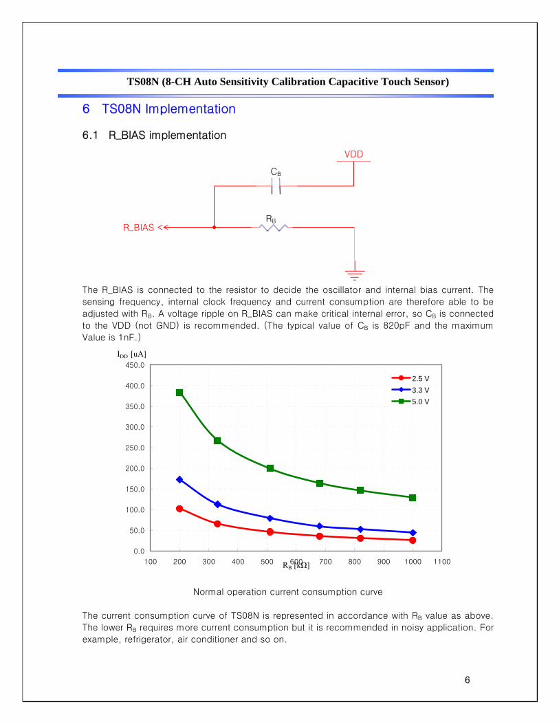
6.1 R_BIAS implementation
6
The R_BIAS is connected to the resistor to decide the oscillator and internal bias current. The
sensing frequency, internal clock frequency and current consumption are therefore able to be
adjusted with RB. A voltage ripple on R_BIAS can make critical internal error, so CB is connected
to the VDD (not GND) is recommended. (The typical value of CB is 820pF and the maximum
Value is 1nF.)
0.0
50.0
100.0
150.0
200.0
250.0
300.0
350.0
400.0
450.0
100 200 300 400 500 600 700 800 900 1000 1100RB [kΩ]
IDD [uA]
2.5 V3.3 V5.0 V
Normal operation current consumption curve
The current consumption curve of TS08N is represented in accordance with RB value as above.
The lower RB requires more current consumption but it is recommended in noisy application. For
example, refrigerator, air conditioner and so on.
R_BIAS << RB
CB
VDD
TS08N (8-CH Auto Sensitivity Calibration Capacitive Touch Sensor)
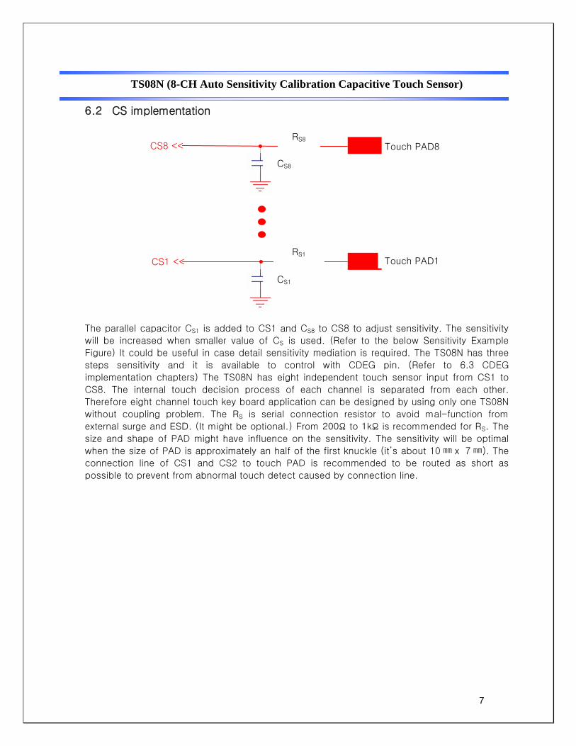
6.2 CS implementation
7
The parallel capacitor CS1 is added to CS1 and CS8 to CS8 to adjust sensitivity. The sensitivity
will be increased when smaller value of CS is used. (Refer to the below Sensitivity Example
Figure) It could be useful in case detail sensitivity mediation is required. The TS08N has three
steps sensitivity and it is available to control with CDEG pin. (Refer to 6.3 CDEG
implementation chapters) The TS08N has eight independent touch sensor input from CS1 to
CS8. The internal touch decision process of each channel is separated from each other.
Therefore eight channel touch key board application can be designed by using only one TS08N
without coupling problem. The RS is serial connection resistor to avoid mal-function from
external surge and ESD. (It might be optional.) From 200Ω to 1kΩ is recommended for RS. The
size and shape of PAD might have influence on the sensitivity. The sensitivity will be optimal
when the size of PAD is approximately an half of the first knuckle (it’s about 10 x 7 ). The
connection line of CS1 and CS2 to touch PAD is recommended to be routed as short as
possible to prevent from abnormal touch detect caused by connection line.
CS8 << RS8
Touch PAD8
CS8
CS1 << RS1
Touch PAD1
CS1
TS08N (8-CH Auto Sensitivity Calibration Capacitive Touch Sensor)
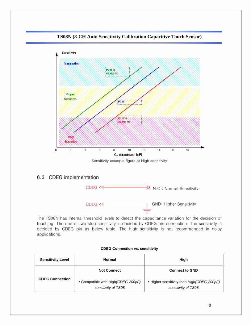
Sensitivity example figure at High sensitivity
6.3 CDEG implementation
8
The TS08N has internal threshold levels to detect the capacitance variation for the decision of
touching. The one of two step sensitivity is decided by CDEG pin connection. The sensitivity is
decided by CDEG pin as below table. The high sensitivity is not recommended in noisy
applications.
CDEG Connection vs. sensitivity
Sensitivity Level Normal High
CDEG Connection
Not Connect
Compatible with High(CDEG 200pF) sensitivity of TS08
Connect to GND
Higher sensitivity than High(CDEG 200pF)sensitivity of TS08
CDEG <<
CDEG << N.C.: Normal Sensitivity
GND: Higher Sensitivity

TS08N (8-CH Auto Sensitivity Calibration Capacitive Touch Sensor)
6.4 SYNC/OPT implementation
6.4.1 Single Connection This pin will be assigned for the output option selection. It will decide that TS08N is working on
single or multi touch detection mode. It should be implemented as below for these.
9
6.4.2 Multi Connection Over two TS08N can work on the one application at the same time thanks to SYNC function
with this pin. The SYNC pulse prevents over two sensing signal from interfering with each other.
RSYNC is pull-down resistor of SYNC/OPT pin. Too big value of RSYNC makes the SYNC pulse
falling delay, and too small value of RSYNC makes rising delay. Typical value of RSYNC is 2MΩ.The
Sync pin should be implemented as below. The TS08N can also be used with the other TSxx
series by employing this SYNC function. The TS08N could only operate on multi output mode in
this configuration.
SYNC/OPT <<
SYNC(/OPT)<<
RSYNC
1 TS08N st
2 TS08N or TS** nd
SYNC/OPT <<
SYNC/OPT <<
VDD
(Single Mode Implementation)
(Multi Mode Implementation)
TS08N (8-CH Auto Sensitivity Calibration Capacitive Touch Sensor)
10
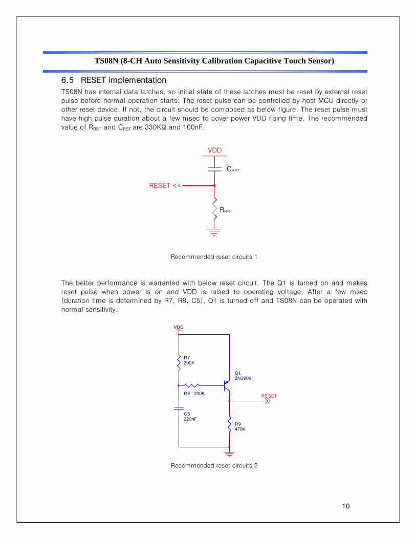
6.5 RESET implementation
TS08N has internal data latches, so initial state of these latches must be reset by external reset
pulse before normal operation starts. The reset pulse can be controlled by host MCU directly or
other reset device. If not, the circuit should be composed as below figure. The reset pulse must
have high pulse duration about a few msec to cover power VDD rising time. The recommended
value of RRST and CRST are 330KΩ and 100nF.
Recommended reset circuits 1
The better performance is warranted with below reset circuit. The Q1 is turned on and makes
reset pulse when power is on and VDD is raised to operating voltage. After a few msec
(duration time is determined by R7, R8, C5), Q1 is turned off and TS08N can be operated with
normal sensitivity.
Recommended reset circuits 2
RESETR8 200K
R7200K
R9470K
Q12N3906
VDD
C5220nF
RESET <<
RRST
CRST
VDD
TS08N (8-CH Auto Sensitivity Calibration Capacitive Touch Sensor)
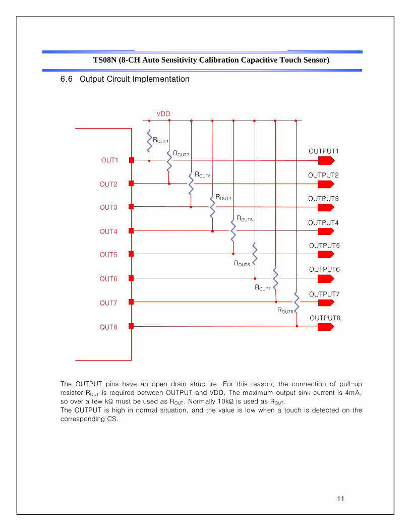
6.6 Output Circuit Implementation
sistor ROUT is required between OUTPUT and VDD. The maximum output sink current is 4mA,
11
The OUTPUT pins have an open drain structure. For this reason, the connection of pull-up
re
so over a few kΩ must be used as ROUT. Normally 10kΩ is used as ROUT.
The OUTPUT is high in normal situation, and the value is low when a touch is detected on the
corresponding CS.
OUT1
ROUT1
VDD
OUTPUT1
OUT2
OUT3
OUT4
OUT5
OUT6
OUT7
ROUT2
OUTPUT2
OUTPUT3
OUTPUT4
OUTPUT5
OUTPUT6
OUTPUT7
OUTPUT8
ROUT3
ROUT4
ROUT5
ROUT6
ROUT7
ROUT8
OUT8

TS08N (8-CH Auto Sensitivity Calibration Capacitive Touch Sensor)
6.7 IMP_SEL (Sense Line Impedance) Implementation
12
The sense input impedance might be selected by the IMP_SEL pin. In case of multi channel
touch sensor application, the sense lines could be drawing side by side with very small gap. In
this case, the sensitivity could be affected by the neighbor channel during out of scanning.
Therefore the connection of IM_SEL pin is recommended to connect with VDD (low impedance
mode). In the other case, the high impedance mode (connection with GND) has an advantage
for sensitivity.
IMP_SEL <<
IMP_SEL <<
VDD
(Sense Line Low Impedance Implementation)
(Sense Line High Impedance Implementation)

TS08N (8-CH Auto Sensitivity Calibration Capacitive Touch Sensor)
7 Recommended Circuit Diagram
13
330k
10pVDD (5V)
OU
TPU
T2
TS08N
3
19
8
5
9
11
67
4
10
12
18
13141516
2021222324
12
17
Cs8
Cs1
Out1
N.C.
Out2
Out4
VssRST
Cdeg
Out3
Cs6Cs7
Vdd
Out6Out7Out8Vss
Cs2Cs3Cs4Rb
Cs5
Out5
Sy nc
OU
TPU
T8
N.C.
10K
10K
200
SEN8
200p
10K
200SEN7SEN6
10K
10p
VDD (5V)
200
10p
VDD (5V)
10p
820p
10K
OU
TPU
T5
10pO
UT
PUT
6
200
SEN1
200
OU
TPU
T4
SEN2
10p
200 SEN3
OU
TPU
T1
510k
2M
SEN4
10p200
10K
10p
VDD (5V)
SEN5
100n
200
OU
TPU
T7
OU
TPU
T3
10K10K
TS08N Application Example Circuit
The VDD periodic voltage ripple over 50mV and the ripple frequency is lower than 10 kHz can
cause wrong sensitivity calibration. To prevent above problem, power (VDD, GND) line of touch circuit should be separated from other circuit. Especially LED driver power line or digital switching circuit power line certainly should be treated to be separated from touch circuit.
When TS08N used in noisy environment, Lower RB is recommended. B
In PCB layout, RB should not be placed on touch pattern. If not, CB BB has to be connected. The RB pattern should be routed as short as possible. B
The CS patterns also should be routed as short as possible and the width of line might be about 0.25mm.
The capacitor that is between VDD and GND is an obligation. It should be located as close as possible from TS08N.
The CS pattern routing should be formed by bottom metal (opposite metal of touch PAD). The empty space of PCB must be filled with GND pattern to strengthen GND pattern and to
prevent external noise from interfere with sensing frequency. The capacitor which is connected with CDEG allows changing the sensitivity. (See 6.3 CDEG
implementation chapter) The TS08N is reset if RST Pin is high. (See 6.5 Reset implementation chapter) The OUT1 ~ OUT8 are open drain output ports. Therefore the pull-up resistor should be
needed as above figure. The TS08N is working with single output mode if SYNC pin is high and it will be in multi output
mode when it’s low. The resistor which is connected with GND should be connected with SYNC pin when the application is required over two TS08N devices.
Connect to the
other TS08N
Note
Note : Refer to 6.3 CDEG Implementation

TS08N (8-CH Auto Sensitivity Calibration Capacitive Touch Sensor)
7.1 Example – Power Line Split Strategy PCB Layout
A. Not split power Line (Bad power line design)
The noise that is generated by AC load or relay can be loaded at 5V power line. A big inductance might be appeared in case of the connection line between main board and
display board is too long, moreover the voltage ripple could be generated by LED (LCD) display driver at VDD (5V).
B. Split power Line (One 5V regulator used) – Recommended
14
C. Split power Line (Separated 5V regulator used) – Strongly recommended

TS08N (8-CH Auto Sensitivity Calibration Capacitive Touch Sensor)
8 MECHANICAL DRAWING
8.1 Mechanical Drawing (24 SOP)
15

TS08N (8-CH Auto Sensitivity Calibration Capacitive Touch Sensor)
8.2 Mechanical Drawing (32 QFN)
16

TS08N (8-CH Auto Sensitivity Calibration Capacitive Touch Sensor)
DIM MIN NOM MAX NOTES A 0.80 0.85 0.90
A1 0.00 0.05 A3 0.203 REF b 0.18 0.23 0.30 D 5.00 BSC E 5.00 BSC
D2 3.20 3.30 3.40 E2 3.20 3.30 3.40 e 0.50 BSC L 0.35 0.40 0.45
L1 - - 0.10 P 45o BSC
aaa 0.15 ccc 0.10
1. ALL DIMENSIONS ARE IN MILLIMETERS. ANGLES ARE IN DEGREES.
2. DIMENSION b APPLIES TO METALLIZED TERMINAL AND IS MEASURED BETWEEN 0.25mm AND 0.30mm FROM TERMINAL TIP. DIMENSION L1 REPRESENTS TERMINAL FULL BACK FROM PACKAGE EDGE UP TO 0.1mm IS ACCEPTABLE.
3. COPLANARITY APPLIES TO THE EXPOSED HEAT SLUG AS WELL AS THE TERMINAL.
4. RADIUS ON TERMINAL IS OPTIONAL.
17

TS08N (8-CH Auto Sensitivity Calibration Capacitive Touch Sensor)
9 MARKING DESCRIPTION
Device Code : T S 0 8 N
Type of version Channel Number Touch Switch Group
Weekly Code : YY ZZ Manufacturing Year Manufacturing Week
18
