transistor design & analysis (inverter) -...
TRANSCRIPT

DIGITAL ELECTRONIC CIRCUIT
M. ZAHID TUFAIL 10-EL-60
Experiment No. 1:
Transistor Design & Analysis (Inverter)
APPARATUS:
Transistor Resistors Connecting Wires Bread Board Dc Power Supply
THEORY:
Digital electronics circuits operate at fixed voltage levels corresponding
to a logical 0 or 1. An inverter circuit serves as the basic logic gate to swap between those two voltage levels. Implementation determines the actual voltage, but common levels include for TTL circuits.
Inverters are available on logic ICs but if you only require one inverter it is usually better to use this circuit. The output signal voltage is the inverse of the input signal:
When the input is high (+Vs) the output is low (0V). When the input is low (0V) the output is high (+Vs).
Any general purpose low power NPN transistor can be used. For general use RB = 10k and RC = 50ohm, then the inverter output can be connected to a device with an input impedance of at least 10k.
If you are connecting the inverter to a CMOS logic IC input with very high impedance you can increase RB to 100k and RC to 10k, this will reduce the current used by the inverter.

DIGITAL ELECTRONIC CIRCUIT
M. ZAHID TUFAIL 10-EL-60
CIRCUIT DIAGRAM:
OBSERVATIONS AND
CALCULATION:
Here, IMAX = 100 mA, VCC = 5 v,
Rc = Vcc /IMAX = 50 Ω VBE = 0.7 v
In our experiment the value of β is 240.
IB = 0.41 mA So,
RB = 10.3 KΩ
Vin Vout 0.0 4.98 0.5 4.90 1 4.16
1.5 3.04 1.8 2.44 2 2.16
2.3 1.90 2.5 1.66 2.8 1.48 3 1.38
3.3 1.28 3.5 1.21 3.8 1.08 4 1.00
4.3 0.91 4.5 0.83 4.8 0.79 5 0.00

DIGITAL ELECTRONIC CIRCUIT
M. ZAHID TUFAIL 10-EL-60
SIMULATED CIRCUIT AND GRAPH:
DIGITAL ELECTRONIC CIRCUIT
M. ZAHID TUFAIL 10-EL-60
Conclusion:
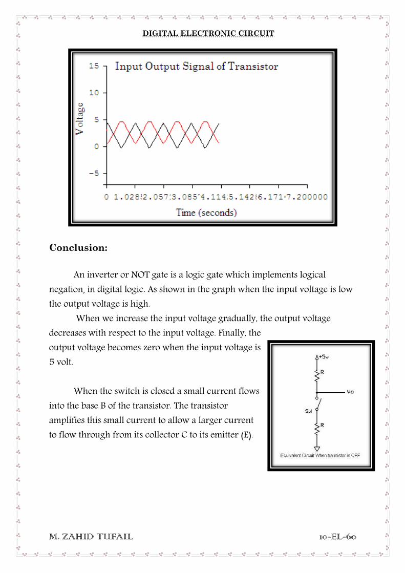
An inverter or NOT gate is a logic gate which implements logical
negation, in digital logic. As shown in the graph when the input voltage is low the output voltage is high.
When we increase the input voltage gradually, the output voltage decreases with respect to the input voltage. Finally, the output voltage becomes zero when the input voltage is 5 volt.
When the switch is closed a small current flows into the base B of the transistor. The transistor amplifies this small current to allow a larger current to flow through from its collector C to its emitter (E).

DIGITAL ELECTRONIC CIRCUIT
M. ZAHID TUFAIL 10-EL-60
When the switch is open no base current flows, so the transistor switches off the collector current.
When the transistor is on, the collector is connected to 0V, the current through the transistor is limited by RC. The Current through the base-emitter junction is limited by RB.
When the transistor is off, no current flows through the transistor, so no voltage is dropped across RC, So the collector is at the supply voltage.
When base is high, collector is low. When base is low, collector is high.

DIGITAL ELECTRONIC CIRCUIT
M. ZAHID TUFAIL 10-EL-60
Experiment No. 2:
To Observe The Noise Margin
& Propagation Delay
APPARATUS:
Transistor Resistors Connecting Wires Bread Board Dc Power Supply
THEORY:
Noise Margin:
Logic gate circuits are designed to input and output only two types of
signals. High (1) and Low (0) are represented by a variable voltage. Full power supply voltage for a High state and zero voltage for a Low state. In a perfect world, all logic circuit signals would exist at these extreme voltage limits, and never deviate from them. However, in reality, logic signal voltage levels rarely attain these perfect limits due to stray voltage drops in the transistor circuitry, and so we must understand the signal level limitations of gate circuits as they try to interpret signal voltages lying somewhere between full supply voltage and zero.
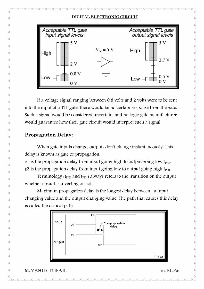
TTL gates operate on a nominal power supply voltage of 5 volts. Ideally, a TTL High signal would be 5.00 volts exactly, and a TTL Low signal 0.00 volts exactly. However, real TTL gate circuits cannot output such perfect voltage levels, and are designed to accept High and Low signals deviating substantially from these ideal values.
Acceptable input signal voltages range from 0 volts to 0.8 volts for a Low logic state, and 2 volts to 5 volts for a High logic state. Acceptable output signal voltages range from 0 volts to 0.5 volts for a Low logic state, and 2.7 volts to 5 volts for a High logic state.
DIGITAL ELECTRONIC CIRCUIT
M. ZAHID TUFAIL 10-EL-60
If a voltage signal ranging between 0.8 volts and 2 volts were to be sent
into the input of a TTL gate, there would be no certain response from the gate. Such a signal would be considered uncertain, and no logic gate manufacturer would guarantee how their gate circuit would interpret such a signal.
Propagation Delay:
When gate inputs change, outputs don’t change instantaneously. This delay is known as gate or propagation. ε1 is the propagation delay from input going high to output going low tPHL. ε2 is the propagation delay from input going low to output going high tPLH.
Terminology (tPHL and tPLH) always refers to the transition on the output whether circuit is inverting or not.
Maximum propagation delay is the longest delay between an input changing value and the output changing value. The path that causes this delay is called the critical path

DIGITAL ELECTRONIC CIRCUIT
M. ZAHID TUFAIL 10-EL-60
Circuit Diagram & Graph:

DIGITAL ELECTRONIC CIRCUIT
M. ZAHID TUFAIL 10-EL-60
Calculations & Observations:
Vin Vout
5 1 0 5
0.5 4.5 1 4
1.5 3.7 2 3.4
2.5 3.1 3 2.5
3.5 2 4 1.8
4.4 1.7 5 0.1

DIGITAL ELECTRONIC CIRCUIT
M. ZAHID TUFAIL 10-EL-60
Conclusions:
The tolerable ranges for output signal levels are narrower than for input
signal levels, to ensure that any TTL gate outputting a digital signal into the input of another TTL gate will transmit voltages acceptable to the receiving gate. The difference between the tolerable output and input ranges is called the noise margin of the gate. For TTL gates, the low-level noise margin is the difference between 0.8 volts and 0.5 volts (0.3 volts), while the high-level noise margin is the difference between 2.7 volts and 2 volts (0.7 volts).
Simply put, the noise margin is the peak amount of spurious or "noise" voltage that may be superimposed on a weak gate output voltage signal before the receiving gate might interpret it wrongly.
In simple words, Noise margin in circuits is the amount of noise that a
circuit can withstand. Propagation delay increases with operating temperature. The largest change in Propagation delay will be due to change in output Load, CL. Normally a typical value of CL is provided in the data sheet, the value for Propagation delay is based on this load. As the load is increased the Propagation delay increases. Some families which provide a Propagation delay number at 50pF [CL] show an increase of 1nS per increase in load. Or, a device may have a 5nS Propagation delay with a 50pF load, 6nS Propagation delay with a 100pF load, a 7nS Propagation delay with a 150pF load and so on.
DIGITAL ELECTRONIC CIRCUIT
M. ZAHID TUFAIL 10-EL-60
Experiment No. 3:
To Observe The Operation Of
Astable Multi-vibrator
APPARATUS:
Op-Amp Resistors Capacitor Connecting Wires Bread Board Dc Power Supply
THEORY:
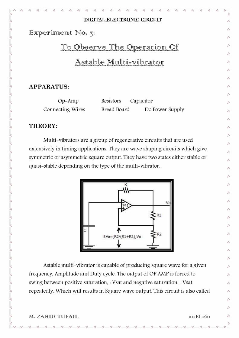
Multi-vibrators are a group of regenerative circuits that are used extensively in timing applications. They are wave shaping circuits which give symmetric or asymmetric square output. They have two states either stable or quasi-stable depending on the type of the multi-vibrator.
Astable multi-vibrator is capable of producing square wave for a given frequency, Amplitude and Duty cycle. The output of OP AMP is forced to swing between positive saturation, +Vsat and negative saturation, -Vsat repeatedly. Which will results in Square wave output. This circuit is also called

DIGITAL ELECTRONIC CIRCUIT
M. ZAHID TUFAIL 10-EL-60
as Free Running Oscillator. Because, it doesn't requires any trigger pulse to get active.
The frequency, f = 1/T , of the square-wave is independent of output voltage Vout. This circuit is also known as free-running or astable multi-vibrator because it has two quasi-stable states. The output remains in one state for time T1 and then makes an abrupt transition to the second state and re-mains in that state for time T2.
The cycle repeats itself after time T = (T1 + T2) where T is the time period of the square-wave. The output of an operational amplifier will be in positive saturation
Vsat, if the differential input voltage is negative and vice versa. The differential voltage, Vd=Vc-βVsat. Where β is the feedback factor and βVsat is the potential at non-inverting terminal of the op amp.
Circuit Diagram:
DIGITAL ELECTRONIC CIRCUIT
M. ZAHID TUFAIL 10-EL-60
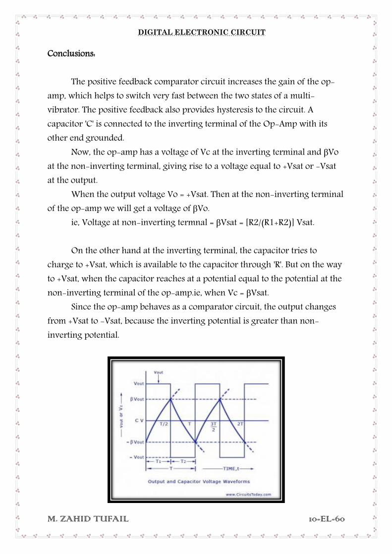
Conclusions: The positive feedback comparator circuit increases the gain of the op-
amp, which helps to switch very fast between the two states of a multi-vibrator. The positive feedback also provides hysteresis to the circuit. A capacitor 'C' is connected to the inverting terminal of the Op-Amp with its other end grounded.
Now, the op-amp has a voltage of Vc at the inverting terminal and βVo at the non-inverting terminal, giving rise to a voltage equal to +Vsat or -Vsat at the output.
When the output voltage Vo = +Vsat. Then at the non-inverting terminal of the op-amp we will get a voltage of βVo.
ie, Voltage at non-inverting termnal = βVsat = [R2/(R1+R2)] Vsat. On the other hand at the inverting terminal, the capacitor tries to
charge to +Vsat, which is available to the capacitor through 'R'. But on the way to +Vsat, when the capacitor reaches at a potential equal to the potential at the non-inverting terminal of the op-amp.ie, when Vc = βVsat.
Since the op-amp behaves as a comparator circuit, the output changes from +Vsat to -Vsat, because the inverting potential is greater than non-inverting potential.

DIGITAL ELECTRONIC CIRCUIT
M. ZAHID TUFAIL 10-EL-60
Now, the output is -Vsat, the feedback voltage reverses the polarity to
-βVsat, which is available at the non-inverting terminal of the op-amp. The capacitor holds a voltage of +βVsat initially at the begining of the second stage, since the output voltage Vo = -Vsat which can flow to the capacitor.
Due to this potential the capacitor tries to discharge to a maximum of
-Vsat, but on the way to -Vsat, when the capacitor reaches a potential equal to the potential of the non-inverting terminal of the op-amp.
ie, when Vc = -βVsat. The comparator circuit changes the output voltage from -Vsat to +Vsat.
Which will repeat in cycles. Astable multivibrator is useful for generating audio frequency signals.

DIGITAL ELECTRONIC CIRCUIT
M. ZAHID TUFAIL 10-EL-60
Experiment No. 4:
To Observe The Operation Of
Mono-stable & Bi-stable Multi-vibrator
APPARATUS:
Op-Amp Resistors Capacitor Connecting Wires Bread Board Dc Power Supply
THEORY:
Mono-Stable:
Multi-vibrators are a group of regenerative circuits that are used
extensively in timing applications. They are wave shaping circuits which give symmetric or asymmetric square output.
They have two states either stable or quasi-stable depending on the type of the multi-vibrator.
Mono-stable multi-vibrator is also called as One Shot Multi-vibrator. A
mono-stable multi-vibrator (MMV) has one stable state and one quasi-stable state. The circuit remains in its stable state till an external triggering pulse causes a transition to the quasi-stable state. After getting the triggering signal the output transit from stable to Quasi-stable state and return back after a time period. So a Single Pulse is generated for single Trigger.
Thus it generates a single output pulse in response to an input pulse and
is referred to as a one shot or single shot. An external trigger signal generated due to charging and discharging of the capacitor produces the transition to the original stable state. So, mono stable multi vibrator is one which generates a single pulse of specified duration in response to each external trigger signal.

DIGITAL ELECTRONIC CIRCUIT
M. ZAHID TUFAIL 10-EL-60
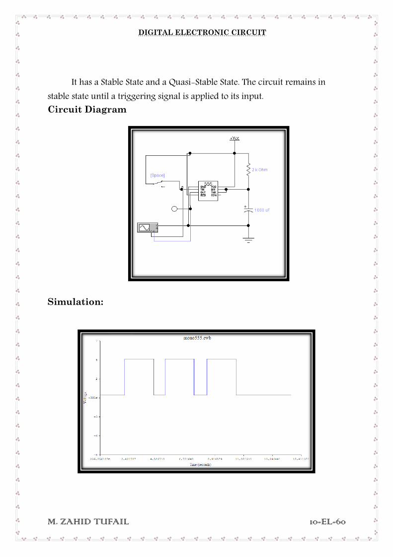
It has a Stable State and a Quasi-Stable State. The circuit remains in stable state until a triggering signal is applied to its input. Circuit Diagram
Bi-Stable:
Bistable multi-vibrator maintains a given out put voltage level unless an
external trigger signal is applied. Application of an external trigger signal causes a change of state, and this output level is maintained indefinitely until a second trigger is applied. Thus it requires two external triggers before it returns to its initial state. So, it has two stable states.
DIGITAL ELECTRONIC CIRCUIT
M. ZAHID TUFAIL 10-EL-60
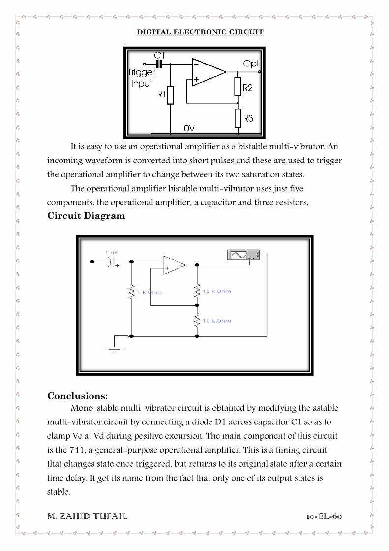
It is easy to use an operational amplifier as a bistable multi-vibrator. An
incoming waveform is converted into short pulses and these are used to trigger the operational amplifier to change between its two saturation states.
The operational amplifier bistable multi-vibrator uses just five components, the operational amplifier, a capacitor and three resistors. Circuit Diagram
Conclusions:
Mono-stable multi-vibrator circuit is obtained by modifying the astable multi-vibrator circuit by connecting a diode D1 across capacitor C1 so as to clamp Vc at Vd during positive excursion. The main component of this circuit is the 741, a general-purpose operational amplifier. This is a timing circuit that changes state once triggered, but returns to its original state after a certain time delay. It got its name from the fact that only one of its output states is stable.

DIGITAL ELECTRONIC CIRCUIT
M. ZAHID TUFAIL 10-EL-60
Under steady-state condition, this circuit will remain in its stable state
with the output Vout = +Vsat and the capacitor C1, is clamped at the voltage VD on-
voltage of diode, D1, i.e. VD = 0.7 V. The voltage VD must be less than (β Vout ) for Vin < 0. The circuit can
be switched to the other state by applying a negative pulse with amplitude greater than (β Vout –
VD) to the non-inverting (+) input terminal. When the negative trigger is applied, the potential at Non-Inverting
terminal becomes less than 0.7v the output switches to -Vsat, which makes the diode more negative than -βVsat. Comparator switches back to +Vsat.
The capacitor C1 now charges exponentially with a time constant
τ = R3C1 toward –Vsat diode Dl being reverse-biased. When capacitor voltage Vc becomes more negative than – βVsat, Vin becomes negative and, therefore, output swings back to +Vsat steady state output.
The capacitor now charges towards +Vsat till Vc attain VD and capacitor
C1 becomes clamped at VD. The width of the trigger pulse Tp is much smaller than the duration of the output pulse T generated. i.e. TP << T.
For reliable operation the circuit should not be triggered again before T. During the quasi-stable state.
At instant t = T and Vc = – β V out Where β = R2/(R1+R2) = Feed back factor
T = 0.693 R3 C1

DIGITAL ELECTRONIC CIRCUIT
M. ZAHID TUFAIL 10-EL-60
The bistable circuit has two stable states. These are the positive and negative saturation voltages of the operational amplifier operating with the given supply voltages. The circuit can then be switched between them by applying pulses. A negative going pulse will switch the circuit into the positive saturation voltage, and a positive going pulse will switch it into the negative state.
Waveforms for the bistable multivibrator operational amplifier circuit It is very easy to calculate the points at which the circuit will trigger.
The positive going pulses need to be greater than -VSat through the potential divider, i.e.
- VSat . (R3 / (R2 + R3)) And similarly the negative going pulses will need to be greater than +VSat through the potential divider, i.e.
+VSat (R3 / (R2 + R3)). If they are not sufficiently large then the bistable will not change state.

DIGITAL ELECTRONIC CIRCUIT
M. ZAHID TUFAIL 10-EL-60
Experiment No. 5 & 6:
To Design and Implement monostable and astable multivibrators using 555 timer I.C.
APPARATUS:
555 ic Resistors Capacitor CRO Connecting Wires Bread Board Dc Power Supply
THEORY:
Mono-Stable:
Multi-vibrators are a group of regenerative circuits that are used
extensively in timing applications. They are wave shaping circuits which give symmetric or asymmetric square output.
They have two states either stable or quasi-stable depending on the type of the multi-vibrator.
Mono-stable multi-vibrator is also called as One Shot Multi-vibrator. A
mono-stable multi-vibrator (MMV) has one stable state and one quasi-stable state. The circuit remains in its stable state till an external triggering pulse causes a transition to the quasi-stable state. After getting the triggering signal the output transit from stable to Quasi-stable state and return back after a time period. So a Single Pulse is generated for single Trigger.
Thus it generates a single output pulse in response to an input pulse and
is referred to as a one shot or single shot. An external trigger signal generated due to charging and discharging of the capacitor produces the transition to the original stable state. So, mono stable multi vibrator is one which generates a single pulse of specified duration in response to each external trigger signal.
DIGITAL ELECTRONIC CIRCUIT
M. ZAHID TUFAIL 10-EL-60
It has a Stable State and a Quasi-Stable State. The circuit remains in stable state until a triggering signal is applied to its input. Circuit Diagram
Simulation:

DIGITAL ELECTRONIC CIRCUIT
M. ZAHID TUFAIL 10-EL-60
AStable:
The astable multivibrator generates a square wave, the period of which
is determined by the circuit external to IC 555. The astable multivibrator does not require any external trigger to change the state of the output. Hence the name free running oscillator. The time during which the output is either high or low is determined by the two resistors and a capacitor which are externally connected to the 555 timer.Initially when the output is high capacitor C starts charging towards Vcc through RA and RB.
However as soon as the voltage across the capacitor equals 2/3 Vcc , comparator1 triggers the flip-flop and the output switches to low state. Now capacitor C discharges through RB and the transistor Q1. When voltage across C equals 1/3 Vcc, comparator 2’s output triggers the flip-flop and the output goes high. Then the cycle repeats. The capacitor is periodically charged and discharged between 2/3 Vcc and 1/3 Vcc respectively. The time during which the capacitor charges from 1/3 Vcc to 2/3 Vcc is equal to the time the output remains high and is given by
where RA and RB are in ohms and C is in Farads. Similarly the time
during which the capacitor discharges from 2/3 Vcc to 1/3 Vccis equal to the time the output is low and is given by
Thus the total time period of the output waveform is

DIGITAL ELECTRONIC CIRCUIT
M. ZAHID TUFAIL 10-EL-60
Circuit Diagram
Simulation:

DIGITAL ELECTRONIC CIRCUIT
M. ZAHID TUFAIL 10-EL-60
Conclusions:
Mono-stable multi-vibrator circuit is obtained by modifying the astable multi-vibrator circuit by disconnecting pin 2 from pin 6. The main component of this circuit is the 555, a general-purpose timer ic. This is a timing circuit that changes state once triggered, but returns to its original state after a certain time delay. It got its name from the fact that only one of its output states is stable.
If we use large value of capacitor, then we will be unable to get ideal
square wave because the fan out of device is low .capacitor is not getting proper current.
For this reason we have to use low value of capacitor, no doubt RC constant will remain same, but small value of capacitor will receive the current quickly.
Across capacitor, voltage charges exponentially. Negative pulse is to provide to disturb its positive level.

DIGITAL ELECTRONIC CIRCUIT
M. ZAHID TUFAIL 10-EL-60
Experiment No. 7:
To make a Trigger circuit with Comparator
APPARATUS:
471 Op-Amp Resistors CRO Connecting Wires Bread Board Dc Power Supply
THEORY:
A circuit or network in which the output changes abruptly with an infinitesimal change in input at a predetermined operating point. Also known as trigger.
A circuit in which an action is initiated by an input pulse, as in a radar modulator. A standard op-amp operating in open-loop configuration (without negative feedback) may be used as a low-performance comparator. When the non-inverting input (V+) is at a higher voltage than the inverting input (V-), the high gain of the op-amp causes the output to saturate at the highest positive voltage it can output. When the non-inverting input (V+) drops below the inverting input (V-), the output saturates at the most negative voltage it can output. The op-amp's output voltage is limited by the supply voltage. An op-amp operating in a linear mode with negative feedback, using a balanced, split-voltage power supply, (powered by ± VS) its transfer function is typically written as: . However, this equation may not be applicable to a comparator circuit which is non-linear and operates open-loop (no negative feedback).
Op-amps are designed to operate in the linear mode with negative
feedback. Hence, an op-amp typically has a lengthy recovery time from saturation. Almost all op-amps have an internal compensation capacitor
DIGITAL ELECTRONIC CIRCUIT
M. ZAHID TUFAIL 10-EL-60
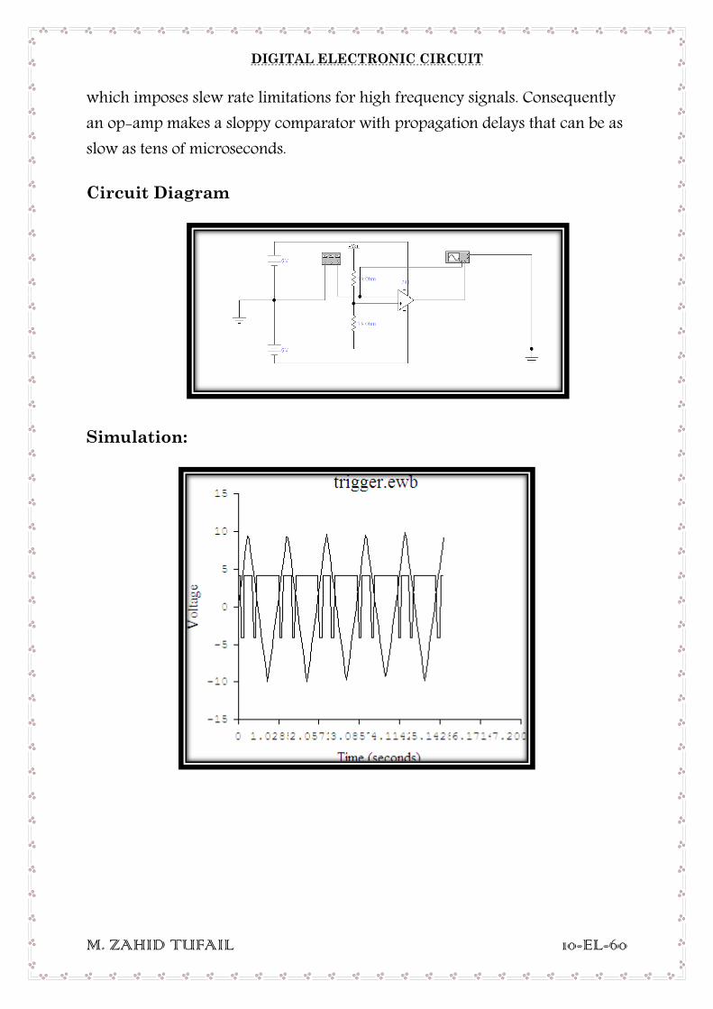
which imposes slew rate limitations for high frequency signals. Consequently an op-amp makes a sloppy comparator with propagation delays that can be as slow as tens of microseconds.
Circuit Diagram
Simulation:

DIGITAL ELECTRONIC CIRCUIT
M. ZAHID TUFAIL 10-EL-60
Conclusions:
A comparator is designed to produce well limited output voltages that easily interface with digital logic. Compatibility with digital logic must be verified while using an op-amp as a comparator.
Op-amps are designed to operate in the linear mode with negative
feedback. Hence, an op-amp typically has a lengthy recovery time from saturation. Almost all op-amps have an internal compensation capacitor which imposes slew rate limitations for high frequency signals. Consequently an op-amp makes a sloppy comparator with propagation delays that can be as slow as tens of microseconds.
A comparator normally changes its output state when the voltage
between its inputs crosses through approximately zero volts. Small voltage fluctuations due to noise, always present on the inputs, can cause undesirable rapid changes between the two output states when the input voltage difference is near zero volts.
Smith trigger can absorb noise which is in range of guard band. In
guard band previous state retains. Smith trigger cannot be formed with input at non inverting terminal of op-amp .because there occur continuous switching on output. We cannot make smith trigger directly. Smith trigger is formed by smith invertor. We attach inverting op-amp in front of smith invertor.

DIGITAL ELECTRONIC CIRCUIT
M. ZAHID TUFAIL 10-EL-60
Experiment No. 8:
To Study and Design the Schmitt Trigger
APPARATUS:
471 Op-Amp Resistors CRO Connecting Wires Bread Board Dc Power Supply
THEORY:
The Schmitt Trigger is a type of comparator with two different threshold voltage levels. Whenever the input voltage goes over the High Threshold Level, the output of the comparator is switched HIGH (if is a standard ST) or LOW (if is an inverting ST). The output will remain in this state, as long as the input voltage is above the second threshold level, the Low Threshold Level. When the input voltage goes below this level, the output of the Schmitt Trigger will switch.
There are basically two symbols for the Schmitt Trigger. The symbol is a triangle with an input and an output, just like the one used for the non-inverting buffers. Inside there is the hysteresis symbol. Depending on the type of Schmitt Trigger, inverting or non-inverting (standard), the hysteresis curve sign differs.
The HIGH and LOW output voltages are actually the POSITIVE and
NEGATIVE power supply voltages of the comparator. The comparator needs to have positive and negative power supply (like + and -) to operate as a Schmitt Trigger normally.

DIGITAL ELECTRONIC CIRCUIT
M. ZAHID TUFAIL 10-EL-60
The Schmitt trigger is a comparator application which switches the output negative when the input passes upward through a positive reference voltage. It then uses negative feedback to prevent switching back to the other state until the input passes through a lower threshold voltage, thus stabilizing the switching against rapid triggering by noise as it passes the trigger point.
Circuit Diagram

DIGITAL ELECTRONIC CIRCUIT
M. ZAHID TUFAIL 10-EL-60
Conclusions:
When the non-inverting input (+) is higher than the inverting input (-), the comparator output switches to the POSITIVE voltage supply. On the contrary, the non-inverting input (+) is lower than the inverting input (-), the output switches to the NEGATIVE voltage supply.
The inverting input (-) is grounded, so someone would expect that the turn-on and off point would be the ground (0). The function of the ST comes from the feedback resistor RFB. When for example the output of the comparator is to the POSITIVE voltage supply, then the non-inverting input has through the RFB this voltage! The same happens when the output is to the NEGATIVE power supply.
The voltage needed to switch the output of the comparator must be above or below zero (ground), according to the POSITIVE and NEGATIVE power supply and according to the resistors RI and RFB. More specific, the formula to calculate the threshold voltage is:
VTHRESHOLD = VSUPPLY x RI RFB + RI
So, if the output is to the POSITIVE voltage, the required negative voltage
that must be applied to Vin is:
VINPUT <= - VTHRESHOLD If the output is to the NEGATIVE voltage, the required positive voltage
that must be applied to Vin is:
VINPUT >= VTHRESHOLD

DIGITAL ELECTRONIC CIRCUIT
M. ZAHID TUFAIL 10-EL-60
Experiment No. 9:
Analysis of the Operation of the Counter Converter
APPARATUS:
ADC Trainer CRO DMM Connecting Wires Dc Power Supply
THEORY:
Most signal we want to process are analog i.e. they are continuous and can take an inifinity of values. Digital systems require discrete digital data. ADC converts an analog information into a digital information. An analog-to-digital converter is a device that converts a continuous physical quantity to a digital number that represents the quantity's amplitude. The conversion involves quantization of the input, so it necessarily introduces a small amount of error. An ADC may also provide an isolated measurement such as an electronic device that converts an input analog voltage or current to a digital number proportional to the magnitude of the voltage or current. However, some non-electronic or only partially electronic devices, such as rotary encoders, can also be considered ADCs.
The digital output may use different coding schemes. Typically the
digital output will be a two's complement binary number that is proportional to the input, but there are other possibilities. An encoder, for example, might output a Gray code.

DIGITAL ELECTRONIC CIRCUIT
M. ZAHID TUFAIL 10-EL-60
Ramp ADC:
One method of addressing the digital ramp ADC's shortcomings is the so-called successive-approximation ADC. The only change in this design is a very special counter circuit known as a successive-approximation register. Instead of counting up in binary sequence, this register counts by trying all values of bits starting with the most-significant bit and finishing at the least-significant bit. Throughout the count process, the register monitors the comparator's output to see if the binary count is less than or greater than the analog signal input, adjusting the bit values accordingly. The way the register counts is identical to the "trial-and-fit" method of decimal-to-binary conversion, whereby different values of bits are tried from MSB to LSB to get a binary number that equals the original decimal number.
A successive-approximation ADC uses a comparator to successively narrow a range that contains the input voltage. At each successive step, the converter compares the input voltage to the output of an internal digital to analog converter which might represent the midpoint of a selected voltage range. At each step in this process, the approximation is stored in a successive approximation register (SAR). For example, consider an input voltage of 6.3 V and the initial range is 0 to 16 V. For the first step, the input 6.3 V is compared to 8 V the midpoint of the 0–16 V range. The comparator reports that the input voltage is less than 8 V, so the SAR is updated to narrow the range to 0–8 V. For the second step, the input voltage is compared to 4 V midpoint of 0–8.

DIGITAL ELECTRONIC CIRCUIT
M. ZAHID TUFAIL 10-EL-60
Observation & Calculation:
Analog input (V)
D3 D2 D1 D0
0.00 0 0 0 0
0.13 0 0 0 1
0.36 0 0 1 0
0.72 0 0 1 1
1.08 0 1 0 0
1.43 0 1 0 1
1.80 0 1 1 0
2.18 0 1 1 1
2.58 1 0 0 0
2.84 1 0 0 1
3.26 1 0 1 0
3.62 1 0 1 1
3.93 1 1 0 0
4.28 1 1 0 1
4.63 1 1 1 0
5.00 1 1 1 1

DIGITAL ELECTRONIC CIRCUIT
M. ZAHID TUFAIL 10-EL-60
Conclusions:
A ramp-compare ADC produces a saw-tooth signal that ramps up or down then quickly returns to zero. When the ramp starts, a timer starts counting. When the ramp voltage matches the input, a comparator fires, and the timer's value is recorded. Timed ramp converters require the least number of transistors. The ramp time is sensitive to temperature because the circuit generating the ramp is often just some simple oscillator. There are two solutions: use a clocked counter driving a DAC and then use the comparator to preserve the counter's value, or calibrate the timed ramp. A special advantage of the ramp-compare system is that comparing a second signal just requires another comparator, and another register to store the voltage value. A very simple (non-linear) ramp-converter can be implemented with a microcontroller and one resistor and capacitor. Vice versa, a filled capacitor can be taken from an integrator, time-to-amplitude converter, phase detector, sample and hold circuit, or peak and hold circuit and discharged. This has the advantage that a slow comparator cannot be disturbed by fast input changes.

DIGITAL ELECTRONIC CIRCUIT
M. ZAHID TUFAIL 10-EL-60
Experiment No. 10:
To Analyze of the Operation of the Monolithic Converter
APPARATUS:
ADC Trainer CRO DMM Connecting Wires Dc Power Supply
THEORY:
Most signal we want to process are analog i.e. they are continuous and can take an inifinity of values. Digital systems require discrete digital data. ADC converts an analog information into a digital information. An analog-to-digital converter is a device that converts a continuous physical quantity to a digital number that represents the quantity's amplitude. The conversion involves quantization of the input, so it necessarily introduces a small amount of error. An ADC may also provide an isolated measurement such as an electronic device that converts an input analog voltage or current to a digital number proportional to the magnitude of the voltage or current. However, some non-electronic or only partially electronic devices, such as rotary encoders, can also be considered ADCs.
The digital output may use different coding schemes. Typically the
digital output will be a two's complement binary number that is proportional to the input, but there are other possibilities. An encoder, for example, might output a Gray code.
DIGITAL ELECTRONIC CIRCUIT
M. ZAHID TUFAIL 10-EL-60
Ramp ADC:
One method of addressing the digital ramp ADC's shortcomings is the so-called successive-approximation ADC. The only change in this design is a very special counter circuit known as a successive-approximation register. Instead of counting up in binary sequence, this register counts by trying all values of bits starting with the most-significant bit and finishing at the least-significant bit. Throughout the count process, the register monitors the comparator's output to see if the binary count is less than or greater than the analog signal input, adjusting the bit values accordingly. The way the register counts is identical to the "trial-and-fit" method of decimal-to-binary conversion, whereby different values of bits are tried from MSB to LSB to get a binary number that equals the original decimal number.
A successive-approximation ADC uses a comparator to successively narrow a range that contains the input voltage. At each successive step, the converter compares the input voltage to the output of an internal digital to analog converter which might represent the midpoint of a selected voltage range. At each step in this process, the approximation is stored in a successive approximation register (SAR). For example, consider an input voltage of 6.3 V and the initial range is 0 to 16 V. For the first step, the input 6.3 V is compared to 8 V the midpoint of the 0–16 V range. The comparator reports that the input voltage is less than 8 V, so the SAR is updated to narrow the range to 0–8 V. For the second step, the input voltage is compared to 4 V midpoint of 0–8.

DIGITAL ELECTRONIC CIRCUIT
M. ZAHID TUFAIL 10-EL-60
Observation & Calculation:
Analog input (V)
D7 D6 D5 D4 D3 D2 D1 D0
0.00 0 0 0 0 0 0 0 0
0.02 0 0 0 0 0 0 0 1
0.04 0 0 0 0 0 0 1 0
0.06 0 0 0 0 0 0 1 1
0.08 0 0 0 0 0 1 0 0
0.10 0 0 0 0 0 1 0 1
0.17 0 0 0 0 1 0 0 1
0.28 0 0 0 0 1 1 1 1
0.45 0 0 0 1 1 0 0 0
0.55 0 0 0 1 1 1 0 1
0.78 0 0 1 0 1 0 0 1
1.19 0 0 1 1 1 1 1 1
1.61 0 1 0 1 0 1 0 1
1.78 0 1 0 1 1 1 1 0
2.64 1 0 0 0 1 0 1 1
3.14 1 0 1 0 0 1 1 0
3.28 1 0 1 0 1 1 0 1
3.58 1 0 1 1 1 1 0 1
4.15 1 1 0 1 1 0 1 1
4.47 1 1 1 0 1 1 0 0

DIGITAL ELECTRONIC CIRCUIT
M. ZAHID TUFAIL 10-EL-60
Conclusions:
A ramp-compare ADC produces a saw-tooth signal that ramps up or down then quickly returns to zero. When the ramp starts, a timer starts counting. When the ramp voltage matches the input, a comparator fires, and the timer's value is recorded. Timed ramp converters require the least number of transistors. The ramp time is sensitive to temperature because the circuit generating the ramp is often just some simple oscillator. There are two solutions: use a clocked counter driving a DAC and then use the comparator to preserve the counter's value, or calibrate the timed ramp. A special advantage of the ramp-compare system is that comparing a second signal just requires another comparator, and another register to store the voltage value. A very simple (non-linear) ramp-converter can be implemented with a microcontroller and one resistor and capacitor. Vice versa, a filled capacitor can be taken from an integrator, time-to-amplitude converter, phase detector, sample and hold circuit, or peak and hold circuit and discharged. This has the advantage that a slow comparator cannot be disturbed by fast input changes.
4.80 1 1 1 1 1 1 0 1
4.84 1 1 1 1 1 1 1 1
DIGITAL ELECTRONIC CIRCUIT
M. ZAHID TUFAIL 10-EL-60
Experiment No. 11:
Analysis of the Operation of the DAC
APPARATUS:
ADC Trainer CRO DMM Connecting Wires Dc Power Supply
THEORY:
In electronics, a digital-to-analog converter (DAC or D-to-A) is a device that converts a digital (usually binary) code to an analog signal (current, voltage, or electric charge). An analog-to-digital converter (ADC) performs the reverse operation. Signals are easily stored and transmitted in digital form, but a DAC is needed for the signal to be recognized by human senses or other non-digital systems.
A common use of digital-to-analog converters is generation of audio signals from digital information in music players. Digital video signals are converted to analog in televisions and mobile phones to display colors and shades. Digital-to-analog conversion can degrade a signal, so conversion details are normally chosen so that the errors are negligible.
Due to cost and the need for matched components, DACs are almost exclusively manufactured on integrated circuits (ICs). There are many DAC architectures which have different advantages and disadvantages. The suitability of a particular DAC for an application is determined by a variety of measurements including speed and resolution.
Instead of impulses, usually the sequence of numbers update the analog voltage at uniform sampling intervals.
These numbers are written to the DAC, typically with a clock signal that causes each number to be latched in sequence, at which time the DAC output voltage changes rapidly from the previous value to the value represented by the currently latched number. The effect of this is that the output voltage is held in time at the current value until the next input number is latched
DIGITAL ELECTRONIC CIRCUIT
M. ZAHID TUFAIL 10-EL-60
resulting in a piecewise constant or 'staircase' shaped output. This is equivalent to a zero-order hold operation and has an effect on the frequency response of the reconstructed signal.
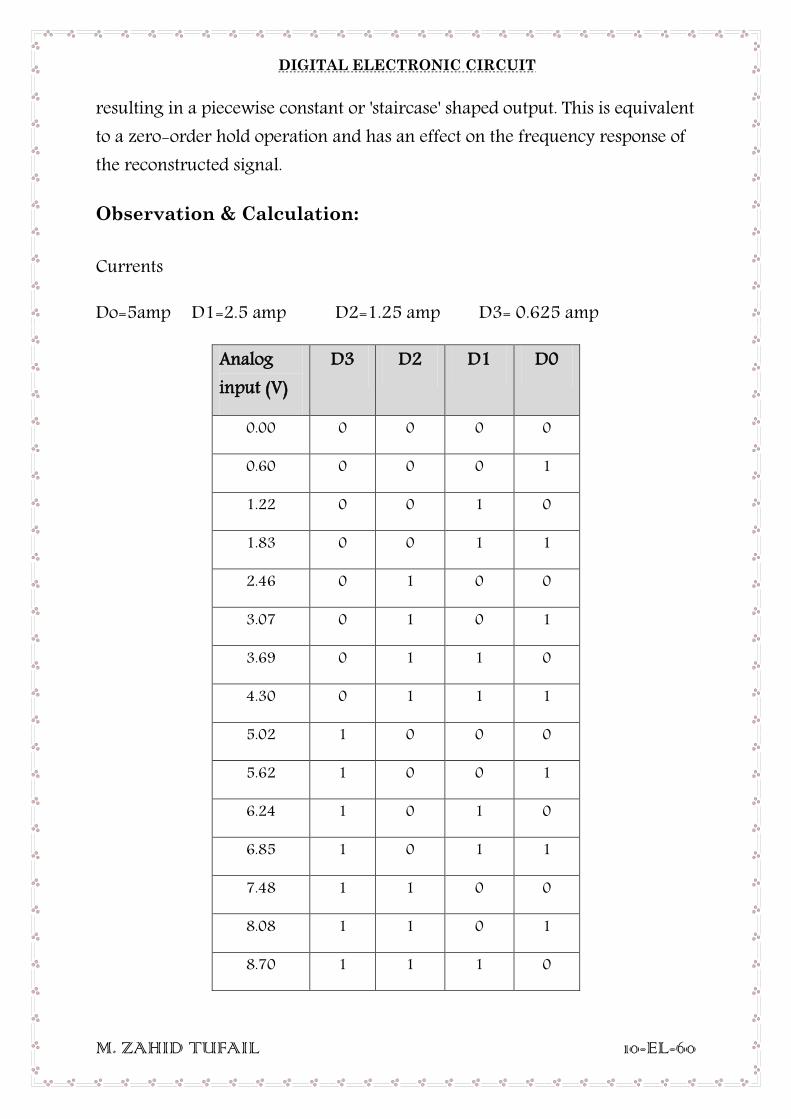
Observation & Calculation:
Currents
Do=5amp D1=2.5 amp D2=1.25 amp D3= 0.625 amp
Analog input (V)
D3 D2 D1 D0
0.00 0 0 0 0
0.60 0 0 0 1
1.22 0 0 1 0
1.83 0 0 1 1
2.46 0 1 0 0
3.07 0 1 0 1
3.69 0 1 1 0
4.30 0 1 1 1
5.02 1 0 0 0
5.62 1 0 0 1
6.24 1 0 1 0
6.85 1 0 1 1
7.48 1 1 0 0
8.08 1 1 0 1
8.70 1 1 1 0

DIGITAL ELECTRONIC CIRCUIT
M. ZAHID TUFAIL 10-EL-60
9.30 1 1 1 1
Ladder network DAC
Analog input (V)
D3 D2 D1 D0
0.00 0 0 0 0
0.64 0 0 0 1
0.96 0 0 1 0
1.29 0 0 1 1
1.48 0 1 0 0
1.88 0 1 0 1
2.05 0 1 1 0
2.27 0 1 1 1
2.58 1 0 0 0
3.23 1 0 0 1
3.55 1 0 1 0
3.88 1 0 1 1
4.07 1 1 0 0
4.48 1 1 0 1

DIGITAL ELECTRONIC CIRCUIT
M. ZAHID TUFAIL 10-EL-60
4.64 1 1 1 0
4.96 1 1 1 1
Conclusions:
The fact that DACs output a sequence of piecewise constant values (known as zero-order hold in sample data textbooks) or rectangular pulses causes multiple harmonics above the Nyquist frequency. Usually, these are removed with a low pass filter acting as a reconstruction filter in applications that require it.
The analog to digital conversion requires two step to perform its process. Quantization Coding Quantization involves the transformation of the continuous analog
signal in a set of discrete values. The quantized signal involves the threshold to be set accurately to divide the range of the signal to be quantize in accurate quantized signals.
Resolution is a term used for the output efficiency of an analog to digital converter which is the number of bits in ADC. While the threshold is defined as (2n – 1) where n represents the number of bits of ADC.
The trainer could be used as a counter or servo analog to digital converter and also as successive approximation analog to digital converter.