supplementary information - media.nature.com · supplementary information for improved performance...
TRANSCRIPT
Supplementary Information for Improved performance and stability in quantum dot solar cells through band alignment engineering Chia-‐Hao M. Chuang1, Patrick R. Brown2, Vladimir Bulović3 & Moungi G. Bawendi4*
1Department of Materials Science and Engineering, 2Department of Physics, 3Department of Electrical Engineering and Computer Science, 4Department of Chemistry, Massachusetts Institute of Technology, Cambridge, Massachusetts, 02139, United States. *email: [email protected]
SUPPLEMENTARY INFORMATIONDOI: 10.1038/NMAT3984
NATURE MATERIALS | www.nature.com/naturematerials 1
© 2014 Macmillan Publishers Limited. All rights reserved.
a
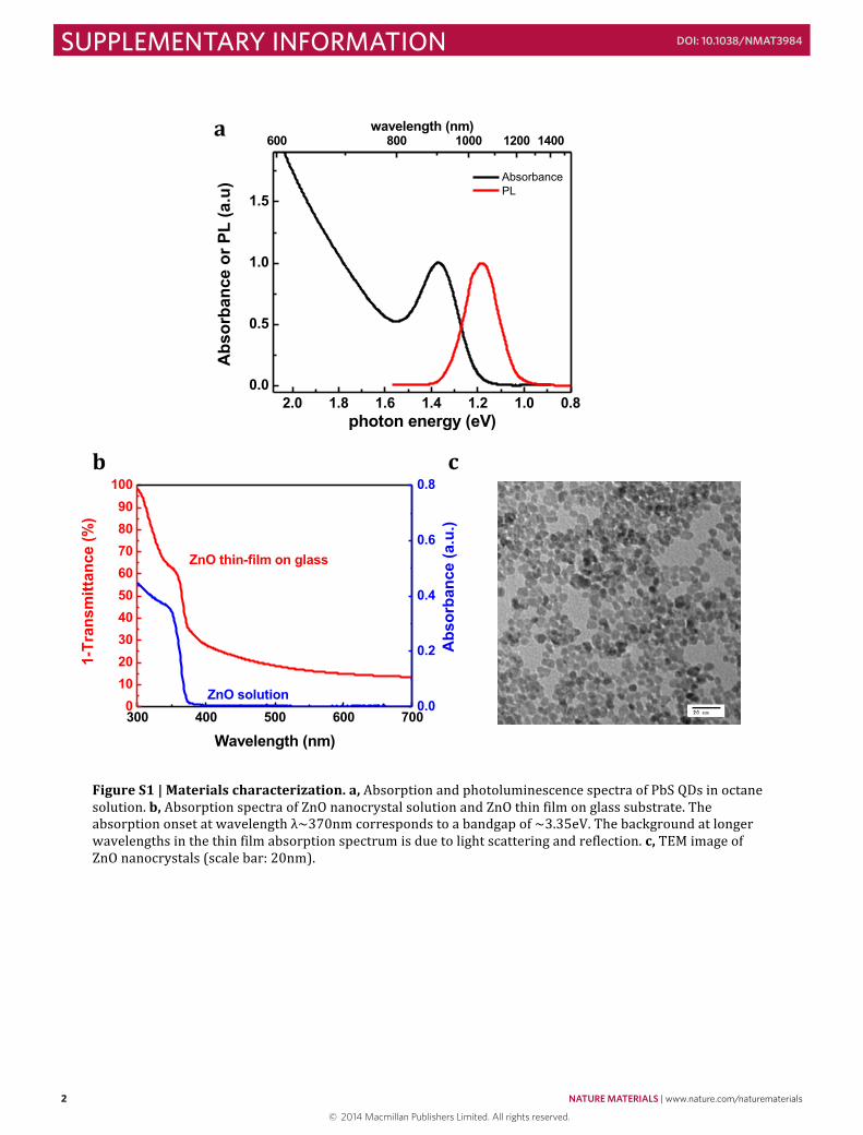
b c Figure S1 | Materials characterization. a, Absorption and photoluminescence spectra of PbS QDs in octane solution. b, Absorption spectra of ZnO nanocrystal solution and ZnO thin film on glass substrate. The absorption onset at wavelength λ~370nm corresponds to a bandgap of ~3.35eV. The background at longer wavelengths in the thin film absorption spectrum is due to light scattering and reflection. c, TEM image of ZnO nanocrystals (scale bar: 20nm).
2.0 1.8 1.6 1.4 1.2 1.0 0.80.0
0.5
1.0
1.5
Abs
orba
nce
or P
L (a
.u)
photon energy (eV)
Absorbance PL
600 800 1000 1200 1400wavelength (nm)
300 400 500 600 7000
102030405060708090
100
1-Tr
ansm
ittan
ce (%
)
Wavelength (nm)
ZnO thin-film on glass
0.0
0.2
0.4
0.6
0.8
ZnO solution
Abs
orba
nce
(a.u
.)
a
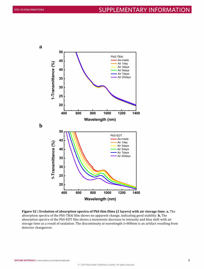
b Figure S2 | Evolution of absorption spectra of PbS thin films (2 layers) with air storage time. a, The absorption spectra of the PbS-‐TBAI film shows no apparent change, indicating good stability. b, The absorption spectra of the PbS-‐EDT film shows a monotonic decrease in intensity and blue shift with air storage time as a result of oxidation. The discontinuity at wavelength λ=800nm is an artifact resulting from detector changeover.
400 600 800 1000 1200 1400
20
25
30
35
40
45
50PbS-TBAI
As-made Air 1day Air 3days Air 5days Air 7days Air 20days
1-Tr
ansm
ittan
ce (%
)
Wavelength (nm)
400 600 800 1000 1200 1400
20
25
30
35
40
45
50PbS-EDT
As-made Air 1day Air 3days Air 5days Air 7days Air 20days
1-Tr
ansm
ittan
ce (%
)
Wavelength (nm)
2 NATURE MATERIALS | www.nature.com/naturematerials
SUPPLEMENTARY INFORMATION DOI: 10.1038/NMAT3984
© 2014 Macmillan Publishers Limited. All rights reserved.
a
b c Figure S1 | Materials characterization. a, Absorption and photoluminescence spectra of PbS QDs in octane solution. b, Absorption spectra of ZnO nanocrystal solution and ZnO thin film on glass substrate. The absorption onset at wavelength λ~370nm corresponds to a bandgap of ~3.35eV. The background at longer wavelengths in the thin film absorption spectrum is due to light scattering and reflection. c, TEM image of ZnO nanocrystals (scale bar: 20nm).
2.0 1.8 1.6 1.4 1.2 1.0 0.80.0
0.5
1.0
1.5
Abs
orba
nce
or P
L (a
.u)
photon energy (eV)
Absorbance PL
600 800 1000 1200 1400wavelength (nm)
300 400 500 600 7000
102030405060708090
100
1-Tr
ansm
ittan
ce (%
)
Wavelength (nm)
ZnO thin-film on glass
0.0
0.2
0.4
0.6
0.8
ZnO solution
Abs
orba
nce
(a.u
.)
a
b Figure S2 | Evolution of absorption spectra of PbS thin films (2 layers) with air storage time. a, The absorption spectra of the PbS-‐TBAI film shows no apparent change, indicating good stability. b, The absorption spectra of the PbS-‐EDT film shows a monotonic decrease in intensity and blue shift with air storage time as a result of oxidation. The discontinuity at wavelength λ=800nm is an artifact resulting from detector changeover.
400 600 800 1000 1200 1400
20
25
30
35
40
45
50PbS-TBAI
As-made Air 1day Air 3days Air 5days Air 7days Air 20days
1-
Tran
smitt
ance
(%)
Wavelength (nm)
400 600 800 1000 1200 1400
20
25
30
35
40
45
50PbS-EDT
As-made Air 1day Air 3days Air 5days Air 7days Air 20days
1-Tr
ansm
ittan
ce (%
)
Wavelength (nm)
NATURE MATERIALS | www.nature.com/naturematerials 3
SUPPLEMENTARY INFORMATIONDOI: 10.1038/NMAT3984
© 2014 Macmillan Publishers Limited. All rights reserved.
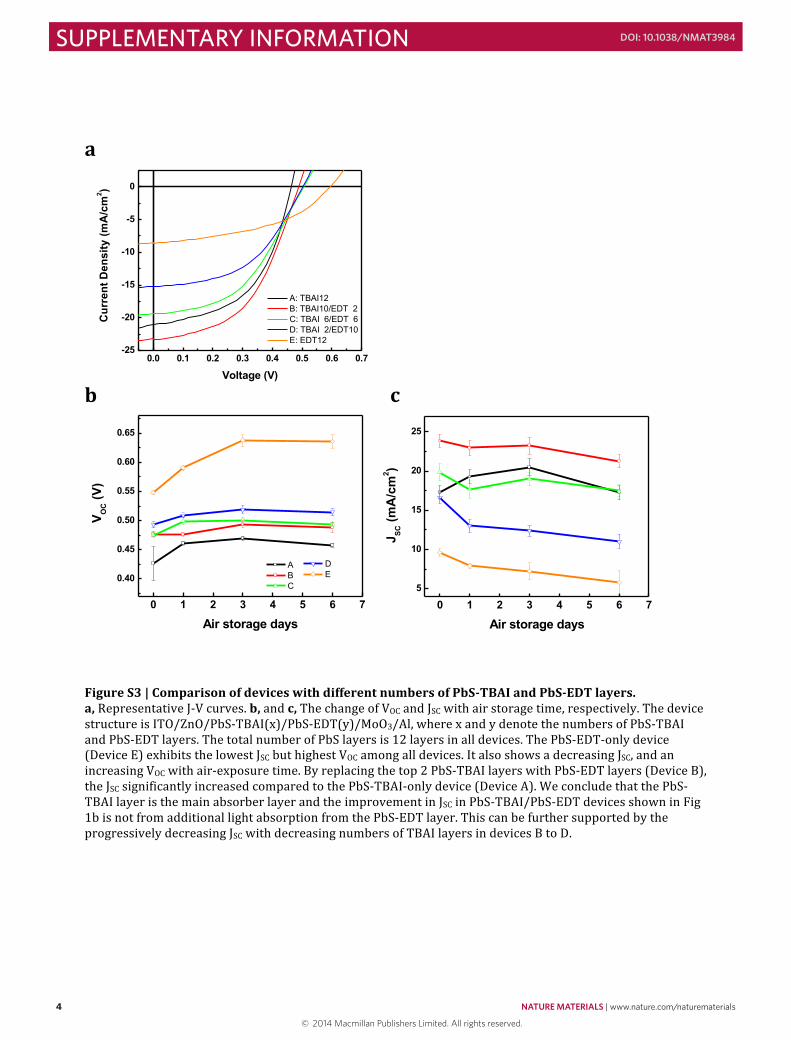
a b c Figure S3 | Comparison of devices with different numbers of PbS-‐TBAI and PbS-‐EDT layers. a, Representative J-‐V curves. b, and c, The change of VOC and JSC with air storage time, respectively. The device structure is ITO/ZnO/PbS-‐TBAI(x)/PbS-‐EDT(y)/MoO3/Al, where x and y denote the numbers of PbS-‐TBAI and PbS-‐EDT layers. The total number of PbS layers is 12 layers in all devices. The PbS-‐EDT-‐only device (Device E) exhibits the lowest JSC but highest VOC among all devices. It also shows a decreasing JSC, and an increasing VOC with air-‐exposure time. By replacing the top 2 PbS-‐TBAI layers with PbS-‐EDT layers (Device B), the JSC significantly increased compared to the PbS-‐TBAI-‐only device (Device A). We conclude that the PbS-‐TBAI layer is the main absorber layer and the improvement in JSC in PbS-‐TBAI/PbS-‐EDT devices shown in Fig 1b is not from additional light absorption from the PbS-‐EDT layer. This can be further supported by the progressively decreasing JSC with decreasing numbers of TBAI layers in devices B to D.
0.0 0.1 0.2 0.3 0.4 0.5 0.6 0.7-25
-20
-15
-10
-5
0
Cur
rent
Den
sity
(mA
/cm
2 )
Voltage (V)
A: TBAI12 B: TBAI10/EDT 2 C: TBAI 6/EDT 6 D: TBAI 2/EDT10 E: EDT12
0 1 2 3 4 5 6 7
0.40
0.45
0.50
0.55
0.60
0.65
D E
A B C
V OC (V
)
Air storage days0 1 2 3 4 5 6 7
5
10
15
20
25
J SC
(mA
/cm
2 )
Air storage days
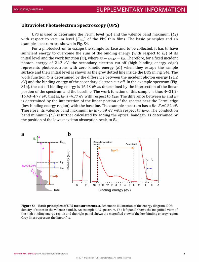
Ultraviolet Photoelectron Spectroscopy (UPS)
UPS is used to determine the Fermi level (EF) and the valence band maximum (EV) with respect to vacuum level (EVAC) of the PbS thin films. The basic principles and an example spectrum are shown in Fig. S4.
For a photoelectron to escape the sample surface and to be collected, it has to have sufficient energy to overcome the sum of the binding energy (with respect to EF) of its initial level and the work function (Φ), where Φ = 𝐸𝐸!"# − 𝐸𝐸! . Therefore, for a fixed incident photon energy of 21.2 eV, the secondary electron cut-‐off (high binding energy edge) represents photoelectrons with zero kinetic energy (Ek) when they escape the sample surface and their initial level is shown as the grey dotted line inside the DOS in Fig. S4a. The work function Φ is determined by the difference between the incident photon energy (21.2 eV) and the binding energy of the secondary electron cut-‐off. In the example spectrum (Fig. S4b), the cut-‐off binding energy is 16.43 eV as determined by the intersection of the linear portion of the spectrum and the baseline. The work function of this sample is thus Φ=21.2-‐16.43=4.77 eV; that is, EF is -‐4.77 eV with respect to EVAC. The difference between EF and EV is determined by the intersection of the linear portion of the spectra near the Fermi edge (low binding energy region) with the baseline. The example spectrum has a EF -‐ EV=0.82 eV. Therefore, its valence band maximum EV is -‐5.59 eV with respect to EVAC. The conduction band minimum (EC) is further calculated by adding the optical bandgap, as determined by the position of the lowest exciton absorption peak, to EV.
a b Figure S4 | Basic principles of UPS measurements. a, Schematic illustration of the energy diagram. DOS: density of states in the valence band. b, An example UPS spectrum. The left panel shows the magnified view of the high binding energy region and the right panel shows the magnified view of the low binding energy region. Grey lines represent the linear fits.
4 NATURE MATERIALS | www.nature.com/naturematerials
SUPPLEMENTARY INFORMATION DOI: 10.1038/NMAT3984
© 2014 Macmillan Publishers Limited. All rights reserved.
a b c Figure S3 | Comparison of devices with different numbers of PbS-‐TBAI and PbS-‐EDT layers. a, Representative J-‐V curves. b, and c, The change of VOC and JSC with air storage time, respectively. The device structure is ITO/ZnO/PbS-‐TBAI(x)/PbS-‐EDT(y)/MoO3/Al, where x and y denote the numbers of PbS-‐TBAI and PbS-‐EDT layers. The total number of PbS layers is 12 layers in all devices. The PbS-‐EDT-‐only device (Device E) exhibits the lowest JSC but highest VOC among all devices. It also shows a decreasing JSC, and an increasing VOC with air-‐exposure time. By replacing the top 2 PbS-‐TBAI layers with PbS-‐EDT layers (Device B), the JSC significantly increased compared to the PbS-‐TBAI-‐only device (Device A). We conclude that the PbS-‐TBAI layer is the main absorber layer and the improvement in JSC in PbS-‐TBAI/PbS-‐EDT devices shown in Fig 1b is not from additional light absorption from the PbS-‐EDT layer. This can be further supported by the progressively decreasing JSC with decreasing numbers of TBAI layers in devices B to D.
0.0 0.1 0.2 0.3 0.4 0.5 0.6 0.7-25
-20
-15
-10
-5
0
Cur
rent
Den
sity
(mA
/cm
2 )
Voltage (V)
A: TBAI12 B: TBAI10/EDT 2 C: TBAI 6/EDT 6 D: TBAI 2/EDT10 E: EDT12
0 1 2 3 4 5 6 7
0.40
0.45
0.50
0.55
0.60
0.65
D E
A B C
V OC (V
)
Air storage days0 1 2 3 4 5 6 7
5
10
15
20
25
J SC (m
A/c
m2 )
Air storage days
Ultraviolet Photoelectron Spectroscopy (UPS)
UPS is used to determine the Fermi level (EF) and the valence band maximum (EV) with respect to vacuum level (EVAC) of the PbS thin films. The basic principles and an example spectrum are shown in Fig. S4.
For a photoelectron to escape the sample surface and to be collected, it has to have sufficient energy to overcome the sum of the binding energy (with respect to EF) of its initial level and the work function (Φ), where Φ = 𝐸𝐸!"# − 𝐸𝐸! . Therefore, for a fixed incident photon energy of 21.2 eV, the secondary electron cut-‐off (high binding energy edge) represents photoelectrons with zero kinetic energy (Ek) when they escape the sample surface and their initial level is shown as the grey dotted line inside the DOS in Fig. S4a. The work function Φ is determined by the difference between the incident photon energy (21.2 eV) and the binding energy of the secondary electron cut-‐off. In the example spectrum (Fig. S4b), the cut-‐off binding energy is 16.43 eV as determined by the intersection of the linear portion of the spectrum and the baseline. The work function of this sample is thus Φ=21.2-‐16.43=4.77 eV; that is, EF is -‐4.77 eV with respect to EVAC. The difference between EF and EV is determined by the intersection of the linear portion of the spectra near the Fermi edge (low binding energy region) with the baseline. The example spectrum has a EF -‐ EV=0.82 eV. Therefore, its valence band maximum EV is -‐5.59 eV with respect to EVAC. The conduction band minimum (EC) is further calculated by adding the optical bandgap, as determined by the position of the lowest exciton absorption peak, to EV.
a b Figure S4 | Basic principles of UPS measurements. a, Schematic illustration of the energy diagram. DOS: density of states in the valence band. b, An example UPS spectrum. The left panel shows the magnified view of the high binding energy region and the right panel shows the magnified view of the low binding energy region. Grey lines represent the linear fits.
NATURE MATERIALS | www.nature.com/naturematerials 5
SUPPLEMENTARY INFORMATIONDOI: 10.1038/NMAT3984
© 2014 Macmillan Publishers Limited. All rights reserved.
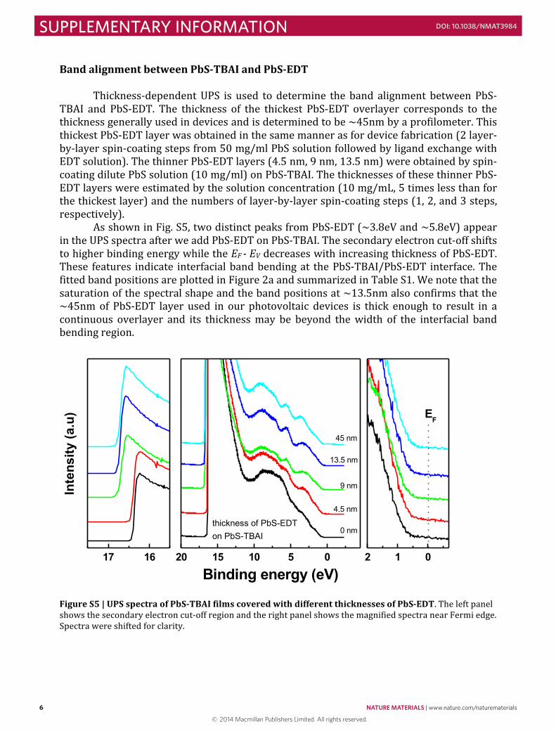
Band alignment between PbS-‐TBAI and PbS-‐EDT Thickness-‐dependent UPS is used to determine the band alignment between PbS-‐
TBAI and PbS-‐EDT. The thickness of the thickest PbS-‐EDT overlayer corresponds to the thickness generally used in devices and is determined to be ~45nm by a profilometer. This thickest PbS-‐EDT layer was obtained in the same manner as for device fabrication (2 layer-‐by-‐layer spin-‐coating steps from 50 mg/ml PbS solution followed by ligand exchange with EDT solution). The thinner PbS-‐EDT layers (4.5 nm, 9 nm, 13.5 nm) were obtained by spin-‐coating dilute PbS solution (10 mg/ml) on PbS-‐TBAI. The thicknesses of these thinner PbS-‐EDT layers were estimated by the solution concentration (10 mg/mL, 5 times less than for the thickest layer) and the numbers of layer-‐by-‐layer spin-‐coating steps (1, 2, and 3 steps, respectively).
As shown in Fig. S5, two distinct peaks from PbS-‐EDT (~3.8eV and ~5.8eV) appear in the UPS spectra after we add PbS-‐EDT on PbS-‐TBAI. The secondary electron cut-‐off shifts to higher binding energy while the EF -‐ EV decreases with increasing thickness of PbS-‐EDT. These features indicate interfacial band bending at the PbS-‐TBAI/PbS-‐EDT interface. The fitted band positions are plotted in Figure 2a and summarized in Table S1. We note that the saturation of the spectral shape and the band positions at ~13.5nm also confirms that the ~45nm of PbS-‐EDT layer used in our photovoltaic devices is thick enough to result in a continuous overlayer and its thickness may be beyond the width of the interfacial band bending region.
Figure S5 | UPS spectra of PbS-‐TBAI films covered with different thicknesses of PbS-‐EDT. The left panel shows the secondary electron cut-‐off region and the right panel shows the magnified spectra near Fermi edge. Spectra were shifted for clarity.
17 16
Inte
nsity
(a.u
)
20 15 10 5 0
13.5 nm
0 nm
45 nm
9 nm
4.5 nm
Binding energy (eV)
thickness of PbS-EDTon PbS-TBAI
EF
2 1 0
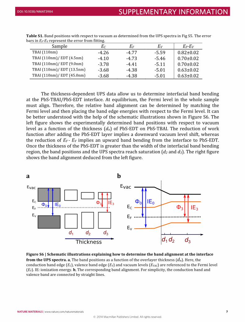
Table S1. Band positions with respect to vacuum as determined from the UPS spectra in Fig S5. The error bars in EF-‐EV represent the error from fitting.
Sample EC EF EV EF-‐EV TBAI (110nm) -‐4.26 -‐4.77 -‐5.59 0.82±0.02 TBAI (110nm)/ EDT (4.5nm) -‐4.10 -‐4.73 -‐5.46 0.70±0.02 TBAI (110nm)/ EDT (9.0nm) -‐3.78 -‐4.41 -‐5.11 0.70±0.02 TBAI (110nm)/ EDT (13.5nm) -‐3.68 -‐4.38 -‐5.01 0.63±0.02 TBAI (110nm)/ EDT (45.0nm) -‐3.68 -‐4.38 -‐5.01 0.63±0.02
The thickness-‐dependent UPS data allow us to determine interfacial band bending at the PbS-‐TBAI/PbS-‐EDT interface. At equilibrium, the Fermi level in the whole sample must align. Therefore, the relative band alignment can be determined by matching the Fermi level and then placing the band edge energies with respect to the Fermi level. It can be better understood with the help of the schematic illustrations shown in Figure S6. The left figure shows the experimentally determined band positions with respect to vacuum level as a function of the thickness (dn) of PbS-‐EDT on PbS-‐TBAI. The reduction of work function after adding the PbS-‐EDT layer implies a downward vacuum level shift, whereas the reduction of EF -‐ EV implies an upward band bending from the interface to PbS-‐EDT. Once the thickness of the PbS-‐EDT is greater than the width of the interfacial band bending region, the band positions and the UPS spectra reach saturation (d2 and d3). The right figure shows the band alignment deduced from the left figure. a b
Figure S6 | Schematic illustrations explaining how to determine the band alignment at the interface from the UPS spectra. a, The band positions as a function of the overlayer thickness (dn). Here, the conduction band edge (EC), valence band edge (EV) and vacuum levels (EVAC) are referenced to the Fermi level (EF). IE: ionization energy. b, The corresponding band alignment. For simplicity, the conduction band and valence band are connected by straight lines.
6 NATURE MATERIALS | www.nature.com/naturematerials
SUPPLEMENTARY INFORMATION DOI: 10.1038/NMAT3984
© 2014 Macmillan Publishers Limited. All rights reserved.
Band alignment between PbS-‐TBAI and PbS-‐EDT Thickness-‐dependent UPS is used to determine the band alignment between PbS-‐
TBAI and PbS-‐EDT. The thickness of the thickest PbS-‐EDT overlayer corresponds to the thickness generally used in devices and is determined to be ~45nm by a profilometer. This thickest PbS-‐EDT layer was obtained in the same manner as for device fabrication (2 layer-‐by-‐layer spin-‐coating steps from 50 mg/ml PbS solution followed by ligand exchange with EDT solution). The thinner PbS-‐EDT layers (4.5 nm, 9 nm, 13.5 nm) were obtained by spin-‐coating dilute PbS solution (10 mg/ml) on PbS-‐TBAI. The thicknesses of these thinner PbS-‐EDT layers were estimated by the solution concentration (10 mg/mL, 5 times less than for the thickest layer) and the numbers of layer-‐by-‐layer spin-‐coating steps (1, 2, and 3 steps, respectively).
As shown in Fig. S5, two distinct peaks from PbS-‐EDT (~3.8eV and ~5.8eV) appear in the UPS spectra after we add PbS-‐EDT on PbS-‐TBAI. The secondary electron cut-‐off shifts to higher binding energy while the EF -‐ EV decreases with increasing thickness of PbS-‐EDT. These features indicate interfacial band bending at the PbS-‐TBAI/PbS-‐EDT interface. The fitted band positions are plotted in Figure 2a and summarized in Table S1. We note that the saturation of the spectral shape and the band positions at ~13.5nm also confirms that the ~45nm of PbS-‐EDT layer used in our photovoltaic devices is thick enough to result in a continuous overlayer and its thickness may be beyond the width of the interfacial band bending region.
Figure S5 | UPS spectra of PbS-‐TBAI films covered with different thicknesses of PbS-‐EDT. The left panel shows the secondary electron cut-‐off region and the right panel shows the magnified spectra near Fermi edge. Spectra were shifted for clarity.
17 16
Inte
nsity
(a.u
)
20 15 10 5 0
13.5 nm
0 nm
45 nm
9 nm
4.5 nm
Binding energy (eV)
thickness of PbS-EDTon PbS-TBAI
EF
2 1 0
Table S1. Band positions with respect to vacuum as determined from the UPS spectra in Fig S5. The error bars in EF-‐EV represent the error from fitting.
Sample EC EF EV EF-‐EV TBAI (110nm) -‐4.26 -‐4.77 -‐5.59 0.82±0.02 TBAI (110nm)/ EDT (4.5nm) -‐4.10 -‐4.73 -‐5.46 0.70±0.02 TBAI (110nm)/ EDT (9.0nm) -‐3.78 -‐4.41 -‐5.11 0.70±0.02 TBAI (110nm)/ EDT (13.5nm) -‐3.68 -‐4.38 -‐5.01 0.63±0.02 TBAI (110nm)/ EDT (45.0nm) -‐3.68 -‐4.38 -‐5.01 0.63±0.02
The thickness-‐dependent UPS data allow us to determine interfacial band bending at the PbS-‐TBAI/PbS-‐EDT interface. At equilibrium, the Fermi level in the whole sample must align. Therefore, the relative band alignment can be determined by matching the Fermi level and then placing the band edge energies with respect to the Fermi level. It can be better understood with the help of the schematic illustrations shown in Figure S6. The left figure shows the experimentally determined band positions with respect to vacuum level as a function of the thickness (dn) of PbS-‐EDT on PbS-‐TBAI. The reduction of work function after adding the PbS-‐EDT layer implies a downward vacuum level shift, whereas the reduction of EF -‐ EV implies an upward band bending from the interface to PbS-‐EDT. Once the thickness of the PbS-‐EDT is greater than the width of the interfacial band bending region, the band positions and the UPS spectra reach saturation (d2 and d3). The right figure shows the band alignment deduced from the left figure. a b
Figure S6 | Schematic illustrations explaining how to determine the band alignment at the interface from the UPS spectra. a, The band positions as a function of the overlayer thickness (dn). Here, the conduction band edge (EC), valence band edge (EV) and vacuum levels (EVAC) are referenced to the Fermi level (EF). IE: ionization energy. b, The corresponding band alignment. For simplicity, the conduction band and valence band are connected by straight lines.
NATURE MATERIALS | www.nature.com/naturematerials 7
SUPPLEMENTARY INFORMATIONDOI: 10.1038/NMAT3984
© 2014 Macmillan Publishers Limited. All rights reserved.
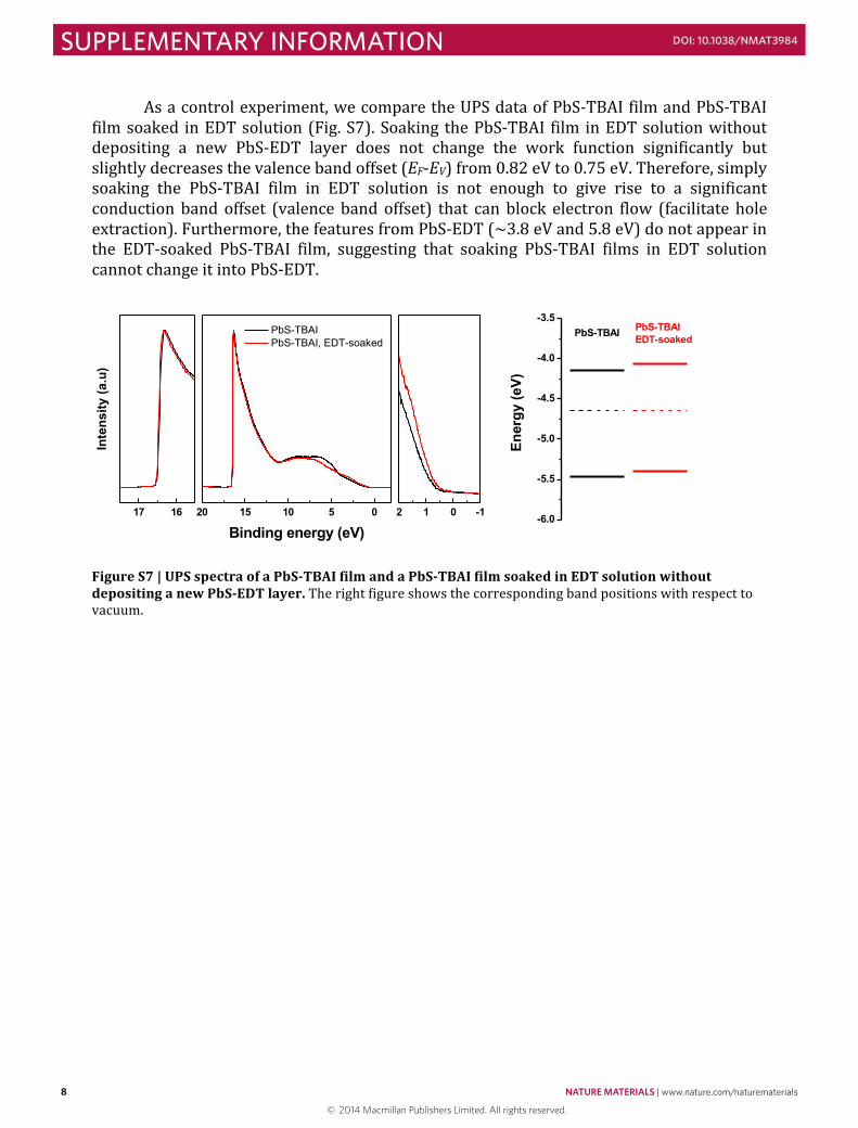
As a control experiment, we compare the UPS data of PbS-‐TBAI film and PbS-‐TBAI film soaked in EDT solution (Fig. S7). Soaking the PbS-‐TBAI film in EDT solution without depositing a new PbS-‐EDT layer does not change the work function significantly but slightly decreases the valence band offset (EF-‐EV) from 0.82 eV to 0.75 eV. Therefore, simply soaking the PbS-‐TBAI film in EDT solution is not enough to give rise to a significant conduction band offset (valence band offset) that can block electron flow (facilitate hole extraction). Furthermore, the features from PbS-‐EDT (~3.8 eV and 5.8 eV) do not appear in the EDT-‐soaked PbS-‐TBAI film, suggesting that soaking PbS-‐TBAI films in EDT solution cannot change it into PbS-‐EDT.
Figure S7 | UPS spectra of a PbS-‐TBAI film and a PbS-‐TBAI film soaked in EDT solution without depositing a new PbS-‐EDT layer. The right figure shows the corresponding band positions with respect to vacuum.
17 16
PbS-TBAI PbS-TBAI, EDT-soaked
Inte
nsity
(a.u
)
20 15 10 5 0
Binding energy (eV)2 1 0 -1
-6.0
-5.5
-5.0
-4.5
-4.0
-3.5PbS-TBAI EDT-soaked
Ener
gy (e
V)
PbS-TBAI
a b
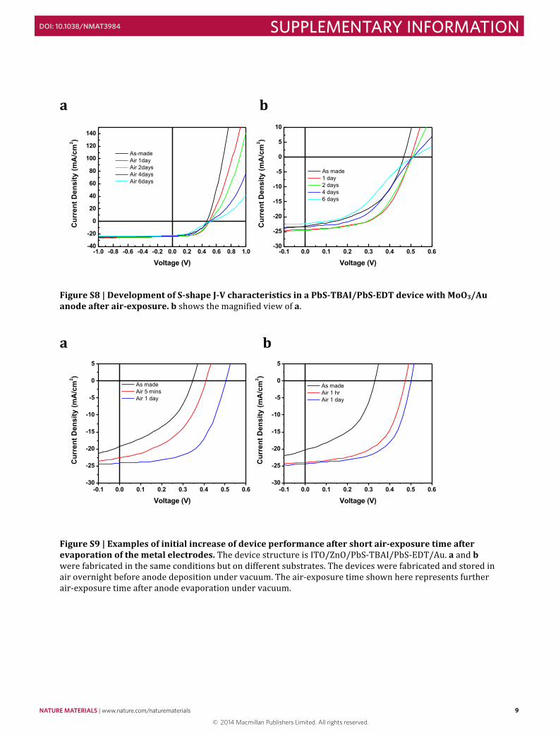
Figure S8 | Development of S-‐shape J-‐V characteristics in a PbS-‐TBAI/PbS-‐EDT device with MoO3/Au anode after air-‐exposure. b shows the magnified view of a.
a b
Figure S9 | Examples of initial increase of device performance after short air-‐exposure time after evaporation of the metal electrodes. The device structure is ITO/ZnO/PbS-‐TBAI/PbS-‐EDT/Au. a and b were fabricated in the same conditions but on different substrates. The devices were fabricated and stored in air overnight before anode deposition under vacuum. The air-‐exposure time shown here represents further air-‐exposure time after anode evaporation under vacuum.
-0.1 0.0 0.1 0.2 0.3 0.4 0.5 0.6-30
-25
-20
-15
-10
-5
0
5
10
Cur
rent
Den
sity
(mA
/cm
2 )
Voltage (V)
As made 1 day 2 days 4 days 6 days
-1.0 -0.8 -0.6 -0.4 -0.2 0.0 0.2 0.4 0.6 0.8 1.0-40
-20
0
20
40
60
80
100
120
140
As-made Air 1day Air 2days Air 4days Air 6days
Cur
rent
Den
sity
(mA
/cm
2 )
Voltage (V)
-0.1 0.0 0.1 0.2 0.3 0.4 0.5 0.6-30
-25
-20
-15
-10
-5
0
5
Cur
rent
Den
sity
(mA
/cm
2 )
Voltage (V)
As made Air 5 mins Air 1 day
-0.1 0.0 0.1 0.2 0.3 0.4 0.5 0.6-30
-25
-20
-15
-10
-5
0
5
As made Air 1 hr Air 1 day
Cur
rent
Den
sity
(mA
/cm
2 )
Voltage (V)
8 NATURE MATERIALS | www.nature.com/naturematerials
SUPPLEMENTARY INFORMATION DOI: 10.1038/NMAT3984
© 2014 Macmillan Publishers Limited. All rights reserved.
As a control experiment, we compare the UPS data of PbS-‐TBAI film and PbS-‐TBAI film soaked in EDT solution (Fig. S7). Soaking the PbS-‐TBAI film in EDT solution without depositing a new PbS-‐EDT layer does not change the work function significantly but slightly decreases the valence band offset (EF-‐EV) from 0.82 eV to 0.75 eV. Therefore, simply soaking the PbS-‐TBAI film in EDT solution is not enough to give rise to a significant conduction band offset (valence band offset) that can block electron flow (facilitate hole extraction). Furthermore, the features from PbS-‐EDT (~3.8 eV and 5.8 eV) do not appear in the EDT-‐soaked PbS-‐TBAI film, suggesting that soaking PbS-‐TBAI films in EDT solution cannot change it into PbS-‐EDT.
Figure S7 | UPS spectra of a PbS-‐TBAI film and a PbS-‐TBAI film soaked in EDT solution without depositing a new PbS-‐EDT layer. The right figure shows the corresponding band positions with respect to vacuum.
17 16
PbS-TBAI PbS-TBAI, EDT-soaked
Inte
nsity
(a.u
)
20 15 10 5 0
Binding energy (eV)2 1 0 -1
-6.0
-5.5
-5.0
-4.5
-4.0
-3.5PbS-TBAI EDT-soaked
Ener
gy (e
V)
PbS-TBAI
a b
Figure S8 | Development of S-‐shape J-‐V characteristics in a PbS-‐TBAI/PbS-‐EDT device with MoO3/Au anode after air-‐exposure. b shows the magnified view of a.
a b
Figure S9 | Examples of initial increase of device performance after short air-‐exposure time after evaporation of the metal electrodes. The device structure is ITO/ZnO/PbS-‐TBAI/PbS-‐EDT/Au. a and b were fabricated in the same conditions but on different substrates. The devices were fabricated and stored in air overnight before anode deposition under vacuum. The air-‐exposure time shown here represents further air-‐exposure time after anode evaporation under vacuum.
-0.1 0.0 0.1 0.2 0.3 0.4 0.5 0.6-30
-25
-20
-15
-10
-5
0
5
10
Cur
rent
Den
sity
(mA
/cm
2 )Voltage (V)
As made 1 day 2 days 4 days 6 days
-1.0 -0.8 -0.6 -0.4 -0.2 0.0 0.2 0.4 0.6 0.8 1.0-40
-20
0
20
40
60
80
100
120
140
As-made Air 1day Air 2days Air 4days Air 6days
Cur
rent
Den
sity
(mA
/cm
2 )
Voltage (V)
-0.1 0.0 0.1 0.2 0.3 0.4 0.5 0.6-30
-25
-20
-15
-10
-5
0
5
Cur
rent
Den
sity
(mA
/cm
2 )
Voltage (V)
As made Air 5 mins Air 1 day
-0.1 0.0 0.1 0.2 0.3 0.4 0.5 0.6-30
-25
-20
-15
-10
-5
0
5
As made Air 1 hr Air 1 day
Cur
rent
Den
sity
(mA
/cm
2 )
Voltage (V)
NATURE MATERIALS | www.nature.com/naturematerials 9
SUPPLEMENTARY INFORMATIONDOI: 10.1038/NMAT3984
© 2014 Macmillan Publishers Limited. All rights reserved.
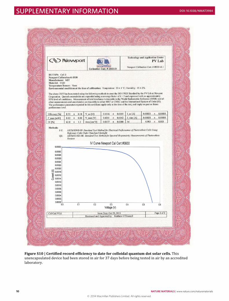
Figure S10 | Certified record efficiency to date for colloidal quantum dot solar cells. This unencapsulated device had been stored in air for 37 days before being tested in air by an accredited laboratory.
Figure S11 | J-‐V characteristics of an unencapsulated PbS-‐TBAI/PbS-‐EDT device with Au anode measured in air and under inert N2-‐atmosphere. No significant difference in performance was found when the device was measured in air. The slight difference is attributed to the different solar simulators used for each measurement and other experimental uncertainties. Figure S12| J-‐V characteristics of devices with different device areas. To test the scalability and reduce the experimental error in determining device area, we fabricated devices with a device area of 5.44 mm2, ~4 times larger than our typical devices (1.24 mm2). The figure plots the J-‐V curves of nine devices with 1.24 mm2 and six devices with 5.44 mm2 area. Devices with a larger device area show similar performance.
-0.6 -0.4 -0.2 0.0 0.2 0.4 0.6-30
-20
-10
0
10
20
30
Cur
rent
Den
sity
(mA
/cm
2 )
Voltage (V)
Measured in air Measured in N2
-0.1 0.0 0.1 0.2 0.3 0.4 0.5 0.6-30
-25
-20
-15
-10
-5
0
5
10
Cur
rent
Den
sity
(mA
/cm
2 )
Voltage (V)
TBAI/EDT/AuDevice area:
1.24 mm2
5.44 mm2
10 NATURE MATERIALS | www.nature.com/naturematerials
SUPPLEMENTARY INFORMATION DOI: 10.1038/NMAT3984
© 2014 Macmillan Publishers Limited. All rights reserved.
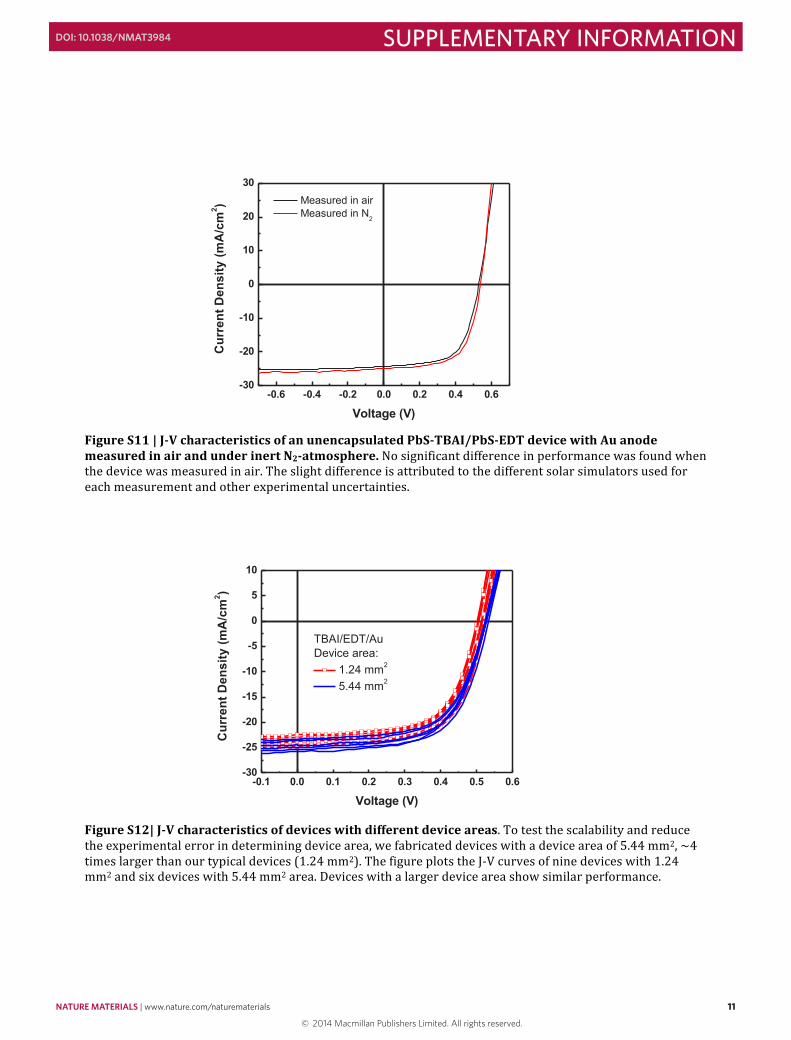
Figure S10 | Certified record efficiency to date for colloidal quantum dot solar cells. This unencapsulated device had been stored in air for 37 days before being tested in air by an accredited laboratory.
Figure S11 | J-‐V characteristics of an unencapsulated PbS-‐TBAI/PbS-‐EDT device with Au anode measured in air and under inert N2-‐atmosphere. No significant difference in performance was found when the device was measured in air. The slight difference is attributed to the different solar simulators used for each measurement and other experimental uncertainties. Figure S12| J-‐V characteristics of devices with different device areas. To test the scalability and reduce the experimental error in determining device area, we fabricated devices with a device area of 5.44 mm2, ~4 times larger than our typical devices (1.24 mm2). The figure plots the J-‐V curves of nine devices with 1.24 mm2 and six devices with 5.44 mm2 area. Devices with a larger device area show similar performance.
-0.6 -0.4 -0.2 0.0 0.2 0.4 0.6-30
-20
-10
0
10
20
30
Cur
rent
Den
sity
(mA
/cm
2 )
Voltage (V)
Measured in air Measured in N2
-0.1 0.0 0.1 0.2 0.3 0.4 0.5 0.6-30
-25
-20
-15
-10
-5
0
5
10
Cur
rent
Den
sity
(mA
/cm
2 )
Voltage (V)
TBAI/EDT/AuDevice area:
1.24 mm2
5.44 mm2
NATURE MATERIALS | www.nature.com/naturematerials 11
SUPPLEMENTARY INFORMATIONDOI: 10.1038/NMAT3984
© 2014 Macmillan Publishers Limited. All rights reserved.
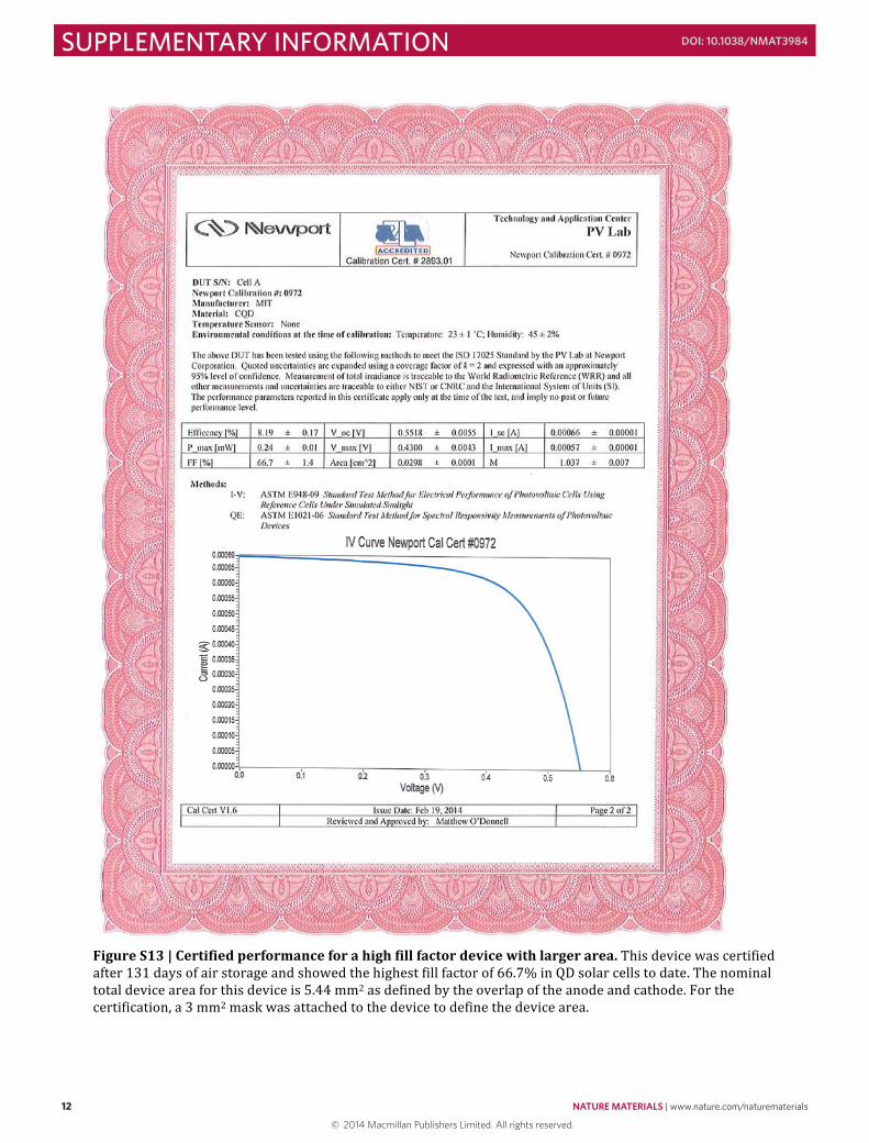
Figure S13 | Certified performance for a high fill factor device with larger area. This device was certified after 131 days of air storage and showed the highest fill factor of 66.7% in QD solar cells to date. The nominal total device area for this device is 5.44 mm2 as defined by the overlap of the anode and cathode. For the certification, a 3 mm2 mask was attached to the device to define the device area.
Figure S14 | Histograms of JSC and power conversion efficiency of devices with MoO3 anodes. The histograms show the performance of devices on different substrates from different batches using the same size of PbS QDs. The PbS-‐TBAI/PbS-‐EDT devices consistently outperform the PbS-‐TBAI devices in every batch of devices we fabricated.
Figure S15 | Histograms of power conversion efficiency of PbS-‐TBAI/PbS-‐EDT devices with Au anodes. The histogram shows the efficiency of more than 30 devices with Au anodes on different substrates. Unlike the devices with MoO3 anodes whose air-‐stability vary due to the uncontrolled ambient humidity, all of the devices with Au anode exhibit excellent air stability.
12 NATURE MATERIALS | www.nature.com/naturematerials
SUPPLEMENTARY INFORMATION DOI: 10.1038/NMAT3984
© 2014 Macmillan Publishers Limited. All rights reserved.
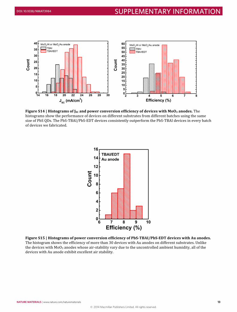
Figure S13 | Certified performance for a high fill factor device with larger area. This device was certified after 131 days of air storage and showed the highest fill factor of 66.7% in QD solar cells to date. The nominal total device area for this device is 5.44 mm2 as defined by the overlap of the anode and cathode. For the certification, a 3 mm2 mask was attached to the device to define the device area.
Figure S14 | Histograms of JSC and power conversion efficiency of devices with MoO3 anodes. The histograms show the performance of devices on different substrates from different batches using the same size of PbS QDs. The PbS-‐TBAI/PbS-‐EDT devices consistently outperform the PbS-‐TBAI devices in every batch of devices we fabricated.
Figure S15 | Histograms of power conversion efficiency of PbS-‐TBAI/PbS-‐EDT devices with Au anodes. The histogram shows the efficiency of more than 30 devices with Au anodes on different substrates. Unlike the devices with MoO3 anodes whose air-‐stability vary due to the uncontrolled ambient humidity, all of the devices with Au anode exhibit excellent air stability.
NATURE MATERIALS | www.nature.com/naturematerials 13
SUPPLEMENTARY INFORMATIONDOI: 10.1038/NMAT3984
© 2014 Macmillan Publishers Limited. All rights reserved.
a
b c
d e
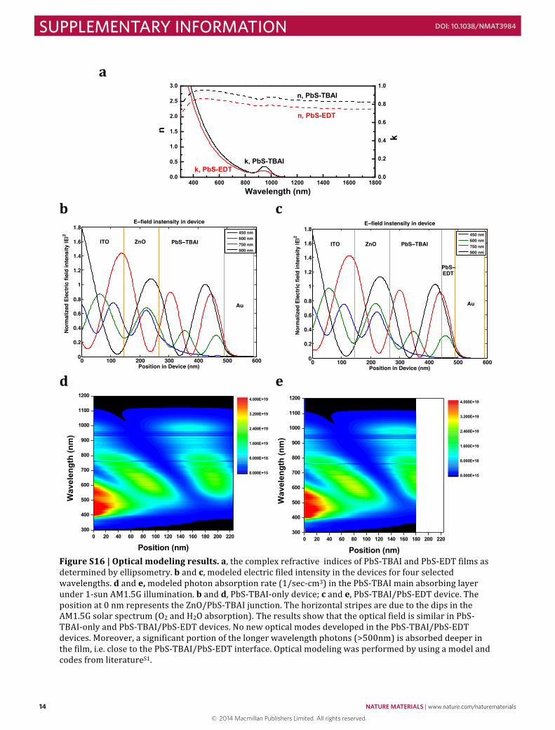
Figure S16 | Optical modeling results. a, the complex refractive indices of PbS-‐TBAI and PbS-‐EDT films as determined by ellipsometry. b and c, modeled electric filed intensity in the devices for four selected wavelengths. d and e, modeled photon absorption rate (1/sec-‐cm3) in the PbS-‐TBAI main absorbing layer under 1-‐sun AM1.5G illumination. b and d, PbS-‐TBAI-‐only device; c and e, PbS-‐TBAI/PbS-‐EDT device. The position at 0 nm represents the ZnO/PbS-‐TBAI junction. The horizontal stripes are due to the dips in the AM1.5G solar spectrum (O2 and H2O absorption). The results show that the optical field is similar in PbS-‐TBAI-‐only and PbS-‐TBAI/PbS-‐EDT devices. No new optical modes developed in the PbS-‐TBAI/PbS-‐EDT devices. Moreover, a significant portion of the longer wavelength photons (>500nm) is absorbed deeper in the film, i.e. close to the PbS-‐TBAI/PbS-‐EDT interface. Optical modeling was performed by using a model and codes from literatureS1.
400 600 800 1000 1200 1400 1600 18000.0
0.5
1.0
1.5
2.0
2.5
3.0
n
Wavelength (nm)
0.0
0.2
0.4
0.6
0.8
1.0
k, PbS-EDTk, PbS-TBAI
n, PbS-EDT
k
n, PbS-TBAI
0 100 200 300 400 500 6000
0.2
0.4
0.6
0.8
1
1.2
1.4
1.6
1.8
ITO ZnO PbS−TBAI
Au
E−field instensity in device
Position in Device (nm)
Nor
mal
ized
Ele
ctric
fiel
d in
tens
ity |E
|2
450 nm600 nm750 nm900 nm
0 100 200 300 400 500 6000
0.2
0.4
0.6
0.8
1
1.2
1.4
1.6
1.8
ITO ZnO PbS−TBAI
PbS−EDT
Au
E−field instensity in device
Position in Device (nm)
Nor
mal
ized
Ele
ctric
fiel
d in
tens
ity |E
|2
450 nm600 nm750 nm900 nm
0 20 40 60 80 100 120 140 160 180 200 220300
400
500
600
700
800
900
1000
1100
1200
Position (nm)
Wav
elen
gth
(nm
)
8.000E+15
8.000E+18
1.600E+19
2.400E+19
3.200E+19
4.000E+19
0 20 40 60 80 100 120 140 160 180 200 220300
400
500
600
700
800
900
1000
1100
1200
Position (nm)
Wav
elen
gth
(nm
)
8.000E+15
8.000E+18
1.600E+19
2.400E+19
3.200E+19
4.000E+19
Reference S1. Burkhard, G. F., Hoke, E. T. & McGehee, M.D. Accounting for interference, scattering, and electrode
absorption to make accurate internal quantum efficiency measurements in organic and other thin solar cells. Adv. Mater. 22, 3293 (2010) ; code: http://www.stanford.edu/group/mcgehee/transfermatrix/index.html.
14 NATURE MATERIALS | www.nature.com/naturematerials
SUPPLEMENTARY INFORMATION DOI: 10.1038/NMAT3984
© 2014 Macmillan Publishers Limited. All rights reserved.

a
b c
d e
Figure S16 | Optical modeling results. a, the complex refractive indices of PbS-‐TBAI and PbS-‐EDT films as determined by ellipsometry. b and c, modeled electric filed intensity in the devices for four selected wavelengths. d and e, modeled photon absorption rate (1/sec-‐cm3) in the PbS-‐TBAI main absorbing layer under 1-‐sun AM1.5G illumination. b and d, PbS-‐TBAI-‐only device; c and e, PbS-‐TBAI/PbS-‐EDT device. The position at 0 nm represents the ZnO/PbS-‐TBAI junction. The horizontal stripes are due to the dips in the AM1.5G solar spectrum (O2 and H2O absorption). The results show that the optical field is similar in PbS-‐TBAI-‐only and PbS-‐TBAI/PbS-‐EDT devices. No new optical modes developed in the PbS-‐TBAI/PbS-‐EDT devices. Moreover, a significant portion of the longer wavelength photons (>500nm) is absorbed deeper in the film, i.e. close to the PbS-‐TBAI/PbS-‐EDT interface. Optical modeling was performed by using a model and codes from literatureS1.
400 600 800 1000 1200 1400 1600 18000.0
0.5
1.0
1.5
2.0
2.5
3.0
n
Wavelength (nm)
0.0
0.2
0.4
0.6
0.8
1.0
k, PbS-EDTk, PbS-TBAI
n, PbS-EDT
k
n, PbS-TBAI
0 100 200 300 400 500 6000
0.2
0.4
0.6
0.8
1
1.2
1.4
1.6
1.8
ITO ZnO PbS−TBAI
Au
E−field instensity in device
Position in Device (nm)
Nor
mal
ized
Ele
ctric
fiel
d in
tens
ity |E
|2
450 nm600 nm750 nm900 nm
0 100 200 300 400 500 6000
0.2
0.4
0.6
0.8
1
1.2
1.4
1.6
1.8
ITO ZnO PbS−TBAI
PbS−EDT
Au
E−field instensity in device
Position in Device (nm)
Nor
mal
ized
Ele
ctric
fiel
d in
tens
ity |E
|2
450 nm600 nm750 nm900 nm
0 20 40 60 80 100 120 140 160 180 200 220300
400
500
600
700
800
900
1000
1100
1200
Position (nm)
Wav
elen
gth
(nm
)
8.000E+15
8.000E+18
1.600E+19
2.400E+19
3.200E+19
4.000E+19
0 20 40 60 80 100 120 140 160 180 200 220300
400
500
600
700
800
900
1000
1100
1200
Position (nm)
Wav
elen
gth
(nm
)
8.000E+15
8.000E+18
1.600E+19
2.400E+19
3.200E+19
4.000E+19
Reference S1. Burkhard, G. F., Hoke, E. T. & McGehee, M.D. Accounting for interference, scattering, and electrode
absorption to make accurate internal quantum efficiency measurements in organic and other thin solar cells. Adv. Mater. 22, 3293 (2010) ; code: http://www.stanford.edu/group/mcgehee/transfermatrix/index.html.
NATURE MATERIALS | www.nature.com/naturematerials 15
SUPPLEMENTARY INFORMATIONDOI: 10.1038/NMAT3984
© 2014 Macmillan Publishers Limited. All rights reserved.