supplementary information - media.nature.com · i o ed. © m publisher l s n a eserved....
TRANSCRIPT

In the format provided by the authors and unedited.
© 2017 Macmillan Publishers Limited, part of Springer Nature. All rights reserved.
SUPPLEMENTARY INFORMATIONDOI: 10.1038/NMAT5038
NATURE MATERIALS | www.nature.com/naturematerials 1
1
Supplementary Information for
Sub-Nanometer Channels Embedded in Two-Dimensional
Materials
Yimo Han1*, Ming-Yang Li2,3*, Gang-Seob Jung4*, Mark A. Marsalis5, Zhao Qin4, Markus
J. Buehler4, Lain-Jong Li2†, David A. Muller1,6†
1. School of Applied & Engineering Physics, Cornell University, Ithaca, NY, 14850, USA 2. Physical Science and Engineering Division, King Abdullah University of Science and Technology, Thuwal, 23955-6900, Kingdom of Saudi Arabia 3. Research Center for Applied Sciences, Academia Sinica, Taipei, 10617, Taiwan 4. Department of Civil and Environmental Engineering, MIT, Cambridge, MA, 02139, USA 5. Department of Physics, Texas Tech University, Lubbock, TX, 79416, USA 6. Kavli Institute at Cornell for Nanoscale Science, Cornell University, Ithaca, NY, 14850, USA
† Corresponding authors: [email protected]; [email protected]

© 2017 Macmillan Publishers Limited, part of Springer Nature. All rights reserved.
NATURE MATERIALS | www.nature.com/naturematerials 2
SUPPLEMENTARY INFORMATIONDOI: 10.1038/NMAT5038
2
Extended Figure 1 | Dislocations at abrupt MoS2-WSe2 junctions. a, Diffraction pattern
of the abrupt junction from a micron-sized area with magnified diffracted spots on the right,
indicating that the two materials are flat and fully relaxed. We fit the peaks to Gaussian and
located the centers, showing a 3.6% lattice mismatch between MoS2 and WSe2. b, Atomic
resolution ADF-STEM image of the abrupt MoS2-WSe2 junction with two misfit
dislocations appearing at the interface. The magnified images of the dislocations are shown
on the right with the atoms marked. They are pentagon-heptagon pair dislocations with Mo-
Mo bonds (red border) or S-S bonds (yellow border). In the formation of 1D MoS2, both
types of the 5|7 dislocations behave similarly as catalysts. c-f, GPA maps of (b), indicating
the lattice strain, in addition to the location and orientation of the misfit dislocations. The
GPA method is discussed in Methods, Extended Fig. 4, and reference 20 in the main
manuscript. g-m, Additional ADF images (g, l) and the overlay with εxx strain maps (h, m)
of abrupt junctions with dislocations at the interface.
© 2017 Macmillan Publishers Limited, part of Springer Nature. All rights reserved.
NATURE MATERIALS | www.nature.com/naturematerials 3
SUPPLEMENTARY INFORMATIONDOI: 10.1038/NMAT5038
3
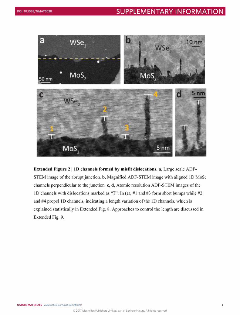
Extended Figure 2 | 1D channels formed by misfit dislocations. a, Large scale ADF-
STEM image of the abrupt junction. b, Magnified ADF-STEM image with aligned 1D MoS2
channels perpendicular to the junction. c, d, Atomic resolution ADF-STEM images of the
1D channels with dislocations marked as “T”. In (c), #1 and #3 form short bumps while #2
and #4 propel 1D channels, indicating a length variation of the 1D channels, which is
explained statistically in Extended Fig. 8. Approaches to control the length are discussed in
Extended Fig. 9.

© 2017 Macmillan Publishers Limited, part of Springer Nature. All rights reserved.
NATURE MATERIALS | www.nature.com/naturematerials 4
SUPPLEMENTARY INFORMATIONDOI: 10.1038/NMAT5038
4
Extended Figure 3 | Color coded ADF-STEM images making lighter Mo and S more
visible. a, Color coded ADF-STEM image of a 1D MoS2 channel with brightness and
contrast optimized to make lighter Mo and S atoms more visible. We observed one sulfur
vacancy (white circle) in this region, showing a sulfur vacancy density of 0.091 nm-2 (1 in
11 nm2). b, Color coded ADF-STEM image of a MoS2 sheet with the same color scale as (a).
We observed three vacancies (white circles), giving a sulfur vacancy density of 0.094 nm-2
(3 in 32 nm2). The comparable density of sulfur vacancies is consistent with the rate of our
electron beam damage (i.e. we lose a few sulfur atoms every scan).

© 2017 Macmillan Publishers Limited, part of Springer Nature. All rights reserved.
NATURE MATERIALS | www.nature.com/naturematerials 5
SUPPLEMENTARY INFORMATIONDOI: 10.1038/NMAT5038
5
Extended Figure 4 | Geometric phase analysis (GPA). a, ADF-STEM showing the 1D
MoS2 channel embedded within WSe2. b, The Fourier transform of a with apertures
indicated by red and blue circles. c, d, The geometric phase images calculated from g1 and
g2 in (b). e, f, The scale of the reciprocal lattice vectors g1 and g2 respectively. g-j, The strain
maps: εxx, εyy, εxy, and rotation respectively. k, The screen capture of the control panel in the
GPA plugin. See Methods for more details.
© 2017 Macmillan Publishers Limited, part of Springer Nature. All rights reserved.
NATURE MATERIALS | www.nature.com/naturematerials 6
SUPPLEMENTARY INFORMATIONDOI: 10.1038/NMAT5038
6
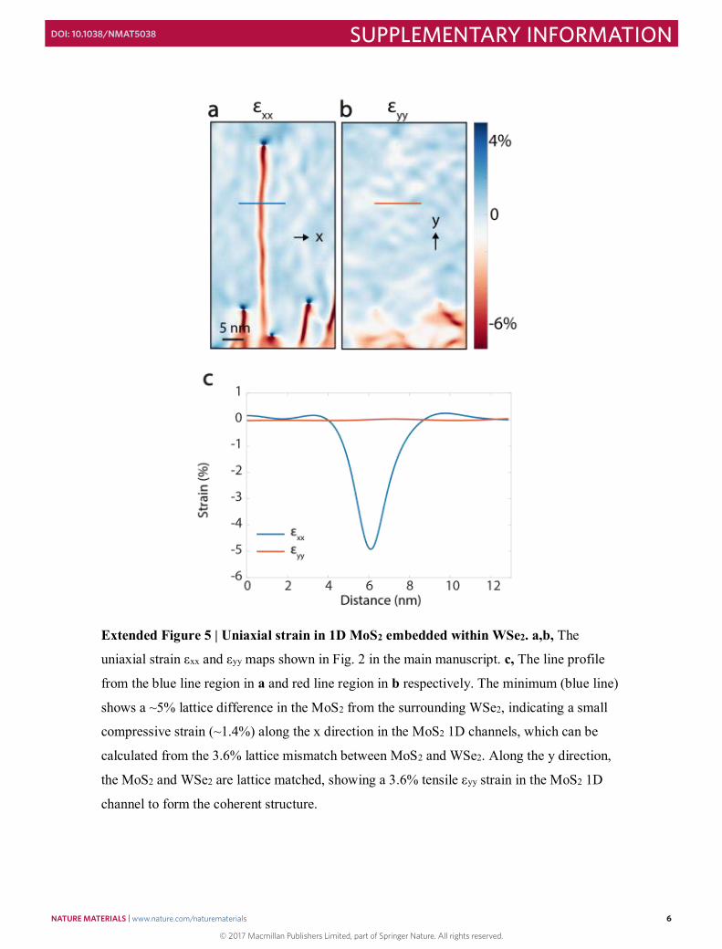
Extended Figure 5 | Uniaxial strain in 1D MoS2 embedded within WSe2. a,b, The
uniaxial strain εxx and εyy maps shown in Fig. 2 in the main manuscript. c, The line profile
from the blue line region in a and red line region in b respectively. The minimum (blue line)
shows a ~5% lattice difference in the MoS2 from the surrounding WSe2, indicating a small
compressive strain (~1.4%) along the x direction in the MoS2 1D channels, which can be
calculated from the 3.6% lattice mismatch between MoS2 and WSe2. Along the y direction,
the MoS2 and WSe2 are lattice matched, showing a 3.6% tensile εyy strain in the MoS2 1D
channel to form the coherent structure.

© 2017 Macmillan Publishers Limited, part of Springer Nature. All rights reserved.
NATURE MATERIALS | www.nature.com/naturematerials 7
SUPPLEMENTARY INFORMATIONDOI: 10.1038/NMAT5038
7
Extended Figure 6 | 1D channels guided by intrinsic dislocations. a, ADF-STEM image
of the 1D channel guided by the intrinsic 5|7 dislocation that is originally embedded within
WSe2. b, The magnified images of the head (tail) of the 1D channel, showing sharp
(alloyed) interfaces. c, The GPA maps from (a), indicating that the dislocation climbs up,
towards its heptagon direction, which is consistent with the 1D channels from interface
dislocations (Fig. 1, 2 and Extended Fig. 2).

© 2017 Macmillan Publishers Limited, part of Springer Nature. All rights reserved.
NATURE MATERIALS | www.nature.com/naturematerials 8
SUPPLEMENTARY INFORMATIONDOI: 10.1038/NMAT5038
8
Extended Figure 7 | Strain guides the migration direction. a-c, Schematic of the 1D
channels migrating via a zigzag path perpendicular to the interface (a), path 30o to the left (b)
and right (c). d-f, The corresponding strain maps of a, b, and c. The strain map of 0o 1D
channel (d) shows a symmetric strain, while (e) and (f) show clear asymmetric strain. g,
Schematic of the catalyst dislocation. h, Table of the local bond angle (θ), atomic strain (ε),
atomic stress (σ) and total energy (E) differentiations between Se1 and Se2 selenium atoms
(g) for the three migrating paths shown in a-c. The initial one is calculated from the case
where the dislocation is at the interface without migrating. The bond angle, strain, and stress
differences between the two W-Se bonds reveal a local asymmetry in the dislocation core.
This asymmetry affects the breaking of left or right W-Se bonds (i.e. migrating toward left
or right) when the precursors insert into the lattice. The comparison of total energy confirms
the dislocation prefers to form a zigzag path that is perpendicular to the interface.

© 2017 Macmillan Publishers Limited, part of Springer Nature. All rights reserved.
NATURE MATERIALS | www.nature.com/naturematerials 9
SUPPLEMENTARY INFORMATIONDOI: 10.1038/NMAT5038
9
Extended Figure 8 | Statistics of 1D channels. a, The histogram of the distance between
two neighboring 1D channels. The average distance is 10.9 (± 0.9) nm, indicating 92 (±8)
1D channels per micron along the MoS2-WSe2 interface. Meanwhile, the measured mean
spacing between dislocations at this interface is 8.3 (± 0.6) nm, indicating a density of 121
(±10) misfit dislocations per micron. This result shows that 76% (± 8%) of the dislocations
tend to migrate and form 1D channels. Errors reported are twice the standard error of the
mean. b, The length distribution of the 1D channels displays an abrupt drop below 2 nm,
suggesting that most 1D channels tend to grow once the catalyst dislocations start to migrate.
Using our current recipe, the longest channel that has been observed is 80 nm. c, The scatter
plot of the channel width according to their length shows that more than 90% of the
channels have widths less than 2 nm. Overall, we ran more than 10 growth rounds and
prepared more than 20 TEM samples. We see 1D channels in all the samples. Our statistics
of the length, width, and neighboring distance are from ~150 1D MoS2 channels. The

© 2017 Macmillan Publishers Limited, part of Springer Nature. All rights reserved.
NATURE MATERIALS | www.nature.com/naturematerials 10
SUPPLEMENTARY INFORMATIONDOI: 10.1038/NMAT5038
10
statistics are taken from the growth condition in Extended Fig. 9c and 9d, where the MoS2
surrounding the WSe2 triangle is micron-meter-sized.
Extended Figure 9 | Controlling the lengths of the 1D channels. a, b, ADF-STEM images
of the 1D channels (a) and the overview of the lateral junction (b). The MoS2 surrounding
the WSe2 triangles is 435 nm (indicated by the yellow arrow) in this sample, while the 1D
channel lengths are only several nanometers. c, d, ADF-STEM images of the sample with
the surrounding MoS2 1.65 µm wide (yellow arrow). The 1D channels are much longer than
those in nanometer-wide MoS2 samples (b). In our study, we focused on samples in this
regime (c and d). To conclude, the dislocation tended to form longer channels with wider
surrounding MoS2 sheets, which can be controlled by the growth time or the precursor ratio
(S:Mo). Slightly increasing the S:Mo ratio helps to grow longer 1D channels. However, S-
excess conditions cause the substitution of the WSe2 layers by MoS2 (ref. 6 in main
manuscript and Extended Fig. 10a and b).

© 2017 Macmillan Publishers Limited, part of Springer Nature. All rights reserved.
NATURE MATERIALS | www.nature.com/naturematerials 11
SUPPLEMENTARY INFORMATIONDOI: 10.1038/NMAT5038
11
Extended Figure 10 | Branching of 1D channels under sulfur excess growth condition.
a, Large field-of-view ADF-STEM image, where the MoS2 replace the some existing WSe2
and form the dendritic shapes at a MoS2-WSe2 junction (the yellow dashed line) in a sulfur
excess growth condition, which was discussed in reference 6 in the main manuscript. The
inset shows the outside MoS2 grows ~10 µm or even more from the WSe2 edges, where the
MoS2 also nucleate and form a second layer on top of WSe2, which are the small brighter
triangles. b, Region with the massive replacements can form periodic wave fronts. c-g,
Catalyst dislocations split into two partial dislocations and form branches. The dislocation
splitting and channel branching process are explained in Extended Fig. 11.

© 2017 Macmillan Publishers Limited, part of Springer Nature. All rights reserved.
NATURE MATERIALS | www.nature.com/naturematerials 12
SUPPLEMENTARY INFORMATIONDOI: 10.1038/NMAT5038
12
Extended Figure 11 | Dislocation splitting and 1D channel branching. a, ADF-STEM
images and their corresponding strain maps of the Y-shaped and fork-shaped junctions. b-e,
Atomic model for the dislocation splitting. The red arrows represent the Burger’s vector,
which is conserved during the splitting process. The black circles indicate the excess Mo and
S atoms inserted into the system during the dislocation splitting process.

© 2017 Macmillan Publishers Limited, part of Springer Nature. All rights reserved.
NATURE MATERIALS | www.nature.com/naturematerials 13
SUPPLEMENTARY INFORMATIONDOI: 10.1038/NMAT5038
13

© 2017 Macmillan Publishers Limited, part of Springer Nature. All rights reserved.
NATURE MATERIALS | www.nature.com/naturematerials 14
SUPPLEMENTARY INFORMATIONDOI: 10.1038/NMAT5038
14
Extended Figure 12 | Electronic properties of 1D MoS2 channels embedded within
WSe2 monolayer. a, DFT calculation of the orbital projected band structure (left) and the
projected density of state (PDOS) (right) of three-unit-cell wide MoS2 1D channel
embedded within WSe2. In the orbital projected band structures, the blue dot lines are
corresponding to the weighted contribution from 1D MoS2, where the dot size is
proportional to the MoS2 contribution. Our calculations show our 1D MoS2 forms a direct
band gap, which is different from the indirect band gap of uniaxially strained MoS2 that has
been reported before (ref. 22 in main manuscript). The gray dot lines are corresponding to
the weighted contribution from the WSe2, while the red lines show the total band structure.
Moreover, the PDOS plots show clear type II band alignment (blue lines) that can
potentially be used for charge separation. b, DFT calculations of 1D MoS2 channels with
two-unit-cell and four-unit-cell width. The band structure and PDOS show little difference
from the three-unit-cell 1D channel, indicating robust 1D confinement even in the presence
of small width variations. We chose the vacuum level as reference (0 eV). The spin-orbital
coupling is not considered in this calculation.

© 2017 Macmillan Publishers Limited, part of Springer Nature. All rights reserved.
NATURE MATERIALS | www.nature.com/naturematerials 15
SUPPLEMENTARY INFORMATIONDOI: 10.1038/NMAT5038
15
Extended Figure 13 | Generation of superlattices. a, Magnified ADF-STEM image from
Fig. 4b with the original WSe2 grain boundary marked with blue dashed lines. The green
arrows indicate the collective migration direction of dislocations. Since the original grain
boundary is not a straight line, the dislocations from the top and bottom parts migrate
towards different directions to form a new straight grain boundary, where all dislocations
tend to lie vertically above one another to achieve the lowest energy. b, The rotation map of
a, showing the new straight grain boundary. c, The overlay of a and b.

© 2017 Macmillan Publishers Limited, part of Springer Nature. All rights reserved.
NATURE MATERIALS | www.nature.com/naturematerials 16
SUPPLEMENTARY INFORMATIONDOI: 10.1038/NMAT5038
16
Extended Figure 14 | MoS2 superlattice forming at a 7o grain boundary in WSe2. a,
ADF-STEM image of the MoS2 superlattice forming at a 7o grain boundary. b, The
diffractogram with the twisted angle measured. c, Another region of the grain boundary. The
low-angle grain boundaries are lines of 5|7 dislocation arrays with the spacing following the
classic dislocation theory d = b/θ, where b is the Burger’s vector and θ is the tilt angle. For
example, at this 7o (0.12 in radians) grain boundary, the dislocation spacing should be 2.77
nm.
© 2017 Macmillan Publishers Limited, part of Springer Nature. All rights reserved.
NATURE MATERIALS | www.nature.com/naturematerials 17
SUPPLEMENTARY INFORMATIONDOI: 10.1038/NMAT5038
17
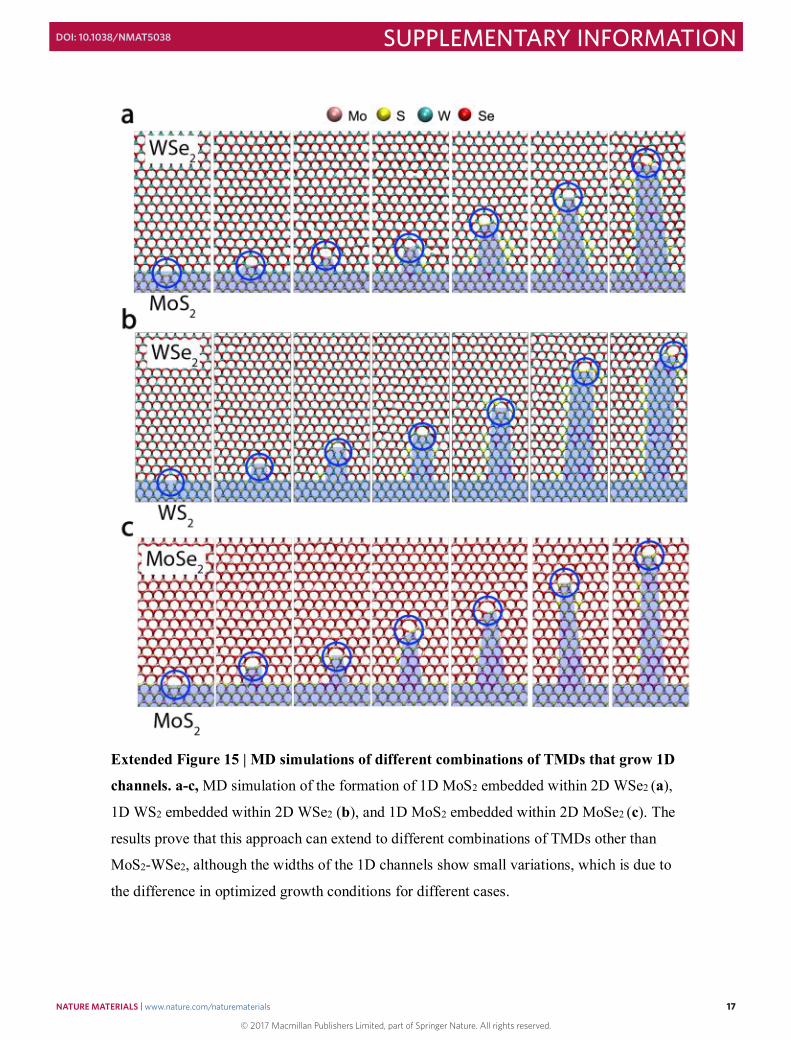
Extended Figure 15 | MD simulations of different combinations of TMDs that grow 1D
channels. a-c, MD simulation of the formation of 1D MoS2 embedded within 2D WSe2 (a),
1D WS2 embedded within 2D WSe2 (b), and 1D MoS2 embedded within 2D MoSe2 (c). The
results prove that this approach can extend to different combinations of TMDs other than
MoS2-WSe2, although the widths of the 1D channels show small variations, which is due to
the difference in optimized growth conditions for different cases.

© 2017 Macmillan Publishers Limited, part of Springer Nature. All rights reserved.
NATURE MATERIALS | www.nature.com/naturematerials 18
SUPPLEMENTARY INFORMATIONDOI: 10.1038/NMAT5038
18
Extended Figure 16 | Lack of 1D channels between MoS2-WS2. a, Atomic-resolution
ADF-STEM image of the MoS2-WS2 lateral heterojunction interface. b, The GPA maps of a,
showing no strain, dislocations, or 1D channels forming at the MoS2-WS2 junction because
the two materials are originally lattice matched.

© 2017 Macmillan Publishers Limited, part of Springer Nature. All rights reserved.
NATURE MATERIALS | www.nature.com/naturematerials 19
SUPPLEMENTARY INFORMATIONDOI: 10.1038/NMAT5038
19
Supplementary Discussion 1: Development of reactive force field for molecular
dynamics.
Molecular Dynamics (MD) simulations in this study were performed via LAMMPS MD
package1 using the Reactive Empirical Bond Order (REBO) force field2-4 to model the
interactions among Mo-W-S-Se atoms in the atomically sharp MoS2-WSe2, WS2-WSe2, and
MoS2-MoSe2 lateral heterojunctions. We utilized the optimized version of Mo-S REBO for
MoS2 monolayer by adjusting radius cutoffs and rescaling the attractive and repulsive terms
of the original form3,4, which have successfully described the experimental observation of
MoS2 monolayer crack propagation with vacancies of sulfides5. We developed W-Se, W-S,
and Mo-Se REBO with the same bond-order parameters of Mo and S but different ionic
radiuses on the basis of their chemical and structural similarities. The REBO force field has
the form
Eb =12
fijC (rij
i¹ jå ) 1+
Qrij
æ
èçö
ø÷Ae-arij - bijBe
-brijé
ëêê
ù
ûúú , (5)
where Eb is the binding energy, fijC (rij ) is a switching function, bij is bond-order term, and
rij is the interatomic distance between atom i and j. We note that Q,a and b , are related to
geometries such as equilibrium distances, A and B are related to the energy of attractive and
repulsive terms. The radius cutoffs of the switching functions are critical to realistic bond
breaking and forming because the functions can cause artificial forces near the failure
points5-7.
We obtained the geometric parameters for MoS2, MoSe2, WS2, and WSe2 from our Density
Functional Theory (DFT) calculations by Quantum-Espresso package8 using Perdew Burke
Ernzerhof (PBE) functional9 and norm-conserving type pseudopotentials10,11. We prepared a
rectangular shape cell containing 6 atoms with the periodic boundary condition in the x
(along the zigzag edge) and y (along the armchair edge) directions. To model each 2D
material, the vacuum space of 15 Å in the z direction is inserted to avoid unphysical
interactions between periodic images. The energy cutoff for the wave functions is 60 Ry and

© 2017 Macmillan Publishers Limited, part of Springer Nature. All rights reserved.
NATURE MATERIALS | www.nature.com/naturematerials 20
SUPPLEMENTARY INFORMATIONDOI: 10.1038/NMAT5038
20
11×11×1 grids are adopted for the K space sampling. Table S1 shows the results of the
geometric parameters of four different monolayers.
The equilibrium distances between Mo-S and W-S are very similar (2.09 and 2.08 Å from
our DFT calculations, respectively). In the REBO forms for MoS2, the equilibrium distance
between sulfides does not affect the lattice constants of monolayers. The difference of lattice
parameters between WS2 and MoS2 mainly comes from the larger ionic radius of W than
Mo. Thus, we parameterized Q,a and b in Eq. (5) of W-W to fit WS2 lattice constants,
while for the FF parameters of W-S we use the same Q,a and b of Mo-S.
Based on the obtained new parameters of W-W, Q,a and b of W-Se were parameterized
to match the lattice parameters of WSe2. In the same way, Q,a and b of Mo-Se are
parameterized. We used Q,a and b of S-S for the parameters of Se-Se because Se-Se/S-S
interaction are not important for the lattice constants of the monolayers. Table S2 shows the
geometric parameters obtained from new REBO force field, which describes the difference
between four different monolayers well.
Afterwards, we re-parameterized A and B, which are related to repulsive and attractive
terms. We followed the same strategy of the previous study5, adjusting radius cut-offs, and
rescaling A and B simultaneously to match stress-strain curves of monolayers, which were
obtained from our DFT calculations (All conditions are the same as those for geometric
parameters). We adjusted the radius cutoffs of the switching functions, fijC (rij ), to match the
failure strains, and rescaled A and B in Eq. (5) to match the stresses at 0.1 strains in the y
direction. The elastic constants from DFT and REBO are shown in Table S3 and S4. The
new parameters well describe the relative differences of four different monolayers.
Finally, we extended the code from handling two atom types (Mo-S) to four different atom
types (Mo-S-W-Se). For Mo-W and S-Se interactions, we used Tersoff potential mixing
rules12 for a , b , A, B and radius cutoffs of the switching functions.

© 2017 Macmillan Publishers Limited, part of Springer Nature. All rights reserved.
NATURE MATERIALS | www.nature.com/naturematerials 21
SUPPLEMENTARY INFORMATIONDOI: 10.1038/NMAT5038
21
DFT (Å) MoS2 WS2 MoSe2 WSe2
Mo/W-Mo/W 3.18 3.23 3.32 3.36
Mo/W-S/Se 2.45 2.45 2.55 2.58
S/Se-S/Se 3.18 3.23 3.32 3.36
t(top-bottom) 3.20 3.19 3.35 3.40
Supplementary Table 1. The geometric parameters obtained from DFT calculations.
REBO (Å) MoS2 WS2 MoSe2 WSe2
Mo/W-Mo/W 3.17 3.24 3.28 3.33
Mo/W-S/Se 2.46 2.46 2.55 2.56
S/Se-S/Se 3.17 3.24 3.28 3.33
t(top-bottom) 3.23 3.21 3.41 3.38
Supplementary Table 2. The geometric parameters obtained from REBO potential
DFT (N/m) MoS2 WS2 MoSe2 WSe2
C11 129.9 129.3 104.7 113.1
C22 130.2 132.6 105.6 112.2
C12 29.25 30.15 24.9 25.8
E 123.5 124 99.2 106.7
Supplementary Table 3. Elastic constants and Young’s modulus (averaged in the x and y
directions) from DFT calculations
REBO (N/m) MoS2 WS2 MoSe2 WSe2
C11 115.1 118.3 90.1 96.3
C22 115.1 118.3 90.1 96.3
C12 34.1 34.8 26.7 28.6
E 105.0 108.1 82.2 87.8
Supplementary Table 4. Elastic constants and Young’s modulus (averaged in the x and y
directions) from the current REBO potential

© 2017 Macmillan Publishers Limited, part of Springer Nature. All rights reserved.
NATURE MATERIALS | www.nature.com/naturematerials 22
SUPPLEMENTARY INFORMATIONDOI: 10.1038/NMAT5038
22
Supplementary Discussion 2: Molecular dynamics model for 1D channels.
We utilized our new REBO force fields for 1D MoS2 channel evolution study. The
computational model is a heterojunction composed of MoS2 (4 nm x 7 nm) and WSe2 (6 nm
x 7 nm) with an interface along the zigzag edge of the 2D lattice. The 7 nm as the length of
the material interface of this heterojunction is naturally given by the ~5% lattice mismatch
between MoS2 and WSe2 (Supplementary Table 1). Periodic boundary conditions were
applied to the zigzag direction along the interface of the heterojunction. Perpendicular to the
interface, the model has 2 nm spacing between the simulation box boundary and the MoS2
edge, and 2 nm spacing for the WSe2 edge from the simulation box boundary. In addition,
we set a 10 nm void region in the out-of-plane direction of the 2D material. These margins
are large enough to guarantee that MoS2 and WSe2 only interact at the interface of the
heterojunction.
We applied an interaction between the bottom layer of S/Se atoms and the substrate by using
a Lennard-Jones (LJ) intermolecular potential with the 9-3 form13 of
𝐸𝐸Sub = 𝜖𝜖 [ 215 (𝜎𝜎
𝑟𝑟)9
− (𝜎𝜎𝑟𝑟)
3], (6)
where r is the distance from an atom to the surface of substrate; 𝜎𝜎 and 𝜖𝜖 are parameters that
relates to the equilibrium distance 𝑟𝑟 = 0.858𝜎𝜎 and adhesion energy 1.054𝜖𝜖 per atom. The
form is related to the integration over a half-lattice of particles with LJ 12-6 intermolecular
potential. In the simulation, we used 𝜎𝜎=2.3 Å and 𝜖𝜖 = 0.1 eV through our simulations. We
chose the adhesion energy as the system is stabilized during the annealing process (See more
details in Supplementary discussion 3). We note that the substrate model is simplified as an
infinite wall to prevent the out-of-plane deformation and the penetration of atoms, which is
similar to the sapphire substrate we used in experiments.
We applied a number of cyclic annealing processes to study the behaviors of the
dislocations. As a result, the pentagon-heptagon dislocations clearly climb towards the
heptagon direction after hundreds of iterations as shown in Extended Fig. 15 and
Supplementary movie #9, which matches our experimental results and represents the

© 2017 Macmillan Publishers Limited, part of Springer Nature. All rights reserved.
NATURE MATERIALS | www.nature.com/naturematerials 23
SUPPLEMENTARY INFORMATIONDOI: 10.1038/NMAT5038
23
dynamic process for 1D MoS2 formation. The supplementary movie #10 and #11 show the
growth for 1D WS2 in WSe2 and 1D MoS2 in MoSe2, indicating that this approach can be
extended to other combinations of transition metal dichalcogenides (TMDs).

© 2017 Macmillan Publishers Limited, part of Springer Nature. All rights reserved.
NATURE MATERIALS | www.nature.com/naturematerials 24
SUPPLEMENTARY INFORMATIONDOI: 10.1038/NMAT5038
24
Supplementary Discussion 3: Annealing process for structural evolution.
A number of cyclic annealing processes with adding or deleting atoms near the dislocation
equilibrate the MoS2-WSe2 model, which is an algorithm combining Monte Carlo and
Molecular Dynamics to accelerate the evolutions of the structures. Each of the cycles is
composed of 4 stages by using NPT or NVT ensemble: heating, relaxing at high
temperature, cooling, and relaxing at low temperature. The periodic condition and NPT
ensemble are applied during the 2nd stage (relaxing at high temperature) to allow the
structural relaxation along the junction direction. We have Tlow=600 K for all atoms, and
Thigh=1100 K for W, Thigh=900 K for Mo and Se, and Thigh=600 K for S with 25 ps for the 2nd
stage and 5 ps for the others. Before the 1st stage (heating) and after the 4th stage (relaxing at
low temperature), conjugate gradient minimizations are applied for 5,000 steps. To simulate
the experimental process of depositing Mo and S precursors at high temperature, we add
MoS2 nanoparticles 3 Å above the Mo/W plane over the dislocation with random variations
less than 1.0 Å in both lattice directions, which allows both simulation efficiency and natural
reaction between the nanoparticles and the MoS2-WSe2 heterojunction to be possible.
After every annealing process, we estimate a position of the next Mo for the most spacious
region. When an estimated Mo position is located 2.4 Å away from the Mo/W atoms, the
precursor nanoparticle (MoS2) is added on the top of the system for the next cycle. The S2 or
S4 is added based on the total number of sulfur and selenium atoms. After the 2nd stage, we
check the out-of-plane displacements of atoms, and delete S/Se above 3.0 Å and Mo/W
above 1.5 Å away from the Mo/W plane. We note that all these processes are setup to
accelerate the reactions without forcibly forming bonds or other structures. The result
confirms the generation of a straight 1D channel from the catalyst 5|7 dislocation with
atomic thickness and reveals the physics behind the growing process in atomic scale. To
predict whether the approach can be applied to other TMDs, similar annealing process was
conducted during the simulation in WS2-WSe2 and MoS2-MoSe2 as well.

© 2017 Macmillan Publishers Limited, part of Springer Nature. All rights reserved.
NATURE MATERIALS | www.nature.com/naturematerials 25
SUPPLEMENTARY INFORMATIONDOI: 10.1038/NMAT5038
25
Supplementary Discussion 4: 1D MoS2 channels step-by-step formation
Extended Movie #1 shows how the precursor nanoparticle (MoS2) around the 5|7 dislocation
inserts into the lattice and forms an intermediate state (Fig. 3a in the main manuscript).
Although the metal precursor comes with sulfur atoms around, in some cases the sulfurs are
released back to the environment due to the lack of the preferable condition. The reaction
can occur with different number of sulfur atoms (movie #2: MoS, movie #3: MoS3,
movie#4: MoS4), but it does not occur without sulfur due to the low coordination number of
molybdenum atom (the Mo bonded to four local S or Se). In this case, the injection is
forbidden, ending with the Mo taking local S or Se out of the system. This is a very
localized reduction around the dislocation region, indicating that the catalyst dislocation
cannot grow 1D channel with little sulfur precursor in the system (movie #5). Moreover, the
precursors away from the catalyst misfit dislocation can’t substitute or insert into the
original lattice, indicating the highly confinement of this dislocation catalyzed approach
(movie #6).
The injection of the metal atom still leaves space for the next coming sulfur atoms to enter
and bond to metal atoms, which may involve breaking and reforming bonds. As a result, the
misfit dislocation climbs. Supplementary movie #7&8 show the side and top view of how
the dislocation climbs up, trying to form the next 5|7 dislocation. In these movies (#7&8),
due to insufficient S in the system, the atoms near the dislocation move actively to find
energetically favorable configuration. During this process, some atoms near the catalyst
dislocation were pushed out of plane and left the system, and the newly introduced
molybdenum or sulfur atoms sometimes substitute the original tungsten or selenium. We
note only atoms near dislocation can be substituted.
We also found that the ratio between the precursors (S:Mo) is critical to stabilize the growth
in MD simulation and form perfect 5|7 dislocation, which is consistent with the growth
conditions in experiments. Sufficient sulfur should be provided to form perfect 5|7
dislocation for the stable and long growth. However, too much sulfur would take too much
pre-existing metal atoms out before forming the next dislocation. We also found the same

© 2017 Macmillan Publishers Limited, part of Springer Nature. All rights reserved.
NATURE MATERIALS | www.nature.com/naturematerials 26
SUPPLEMENTARY INFORMATIONDOI: 10.1038/NMAT5038
26
mechanisms with other combination of TMDs, such as 1D WS2 channel embedded in WSe2
and 1D MoS2 embedded in MoSe2 (Movie #10&11).
We summarized and simplified the entire process into four main steps:
1) Insertion of the Mo atom from precursors at the 5|7 catalyst dislocation.
2) Reconstruction and relaxation of the structure with more S precursor atoms to form the
next 5|7 dislocation.
3) Repeat the process to form 1D channels.

© 2017 Macmillan Publishers Limited, part of Springer Nature. All rights reserved.
NATURE MATERIALS | www.nature.com/naturematerials 27
SUPPLEMENTARY INFORMATIONDOI: 10.1038/NMAT5038
27
Supplementary discussion 5: DFT calculation of 1D MoS2 channel embedded in WSe2
To demonstrate possible applications of 1D MoS2 channel embedded in WSe2, we obtained
orbital projected band structures and projected density of state (PDOS) of six different
models by QE package using the same functional and pseudopotentials used for geometric
parameters in Supplementary Discussion 1. The rectangular shape unit cells are replicated in
the x direction containing 60 atoms with the periodic boundary condition in the x (along the
zigzag edge) and y (along the armchair edge) directions. The energy cutoff for the wave
functions is set to 60 Ry and 2×8×1 and 4x32x1 Monkhost-Pack grids are adopted for the K
space sampling for structure relaxation and PDOS, respectively. We prepare 6 models with
different ratios of MoS2 and WSe2 to represent 1D MoS2 channels. The cells and atomistic
structures are fully relaxed with convergence thresholds of 0.5 kbar and 10-3 (a.u.) for the
pressure and atomic forces, respectively. Due to the rectangular unit shape of the system, we
used Γ-Κ-Υ-Γ for the bands structure to see the difference between the gap at the Γ the K
points in hexagonal Brillouin zone (BZ) as suggested in the previous study14. Absolute
conduction band minimum (CBM) and valence band maximum (VBM) relative to the
vacuum level are calculated for all models. The obtained energy levels of pristine MoS2 and
WSe2 show good agreement with those from the previous study15, confirming the reliability
of our calculation.
From the orbital projected band structures and PDOS shown in Extended Fig 16, the 1D
channel of MoS2 mainly contributes to the CBM and the major contribution for the VBM
comes from WSe2. To estimate the local band gaps of MoS2, we evaluated the contributions
of MoS2 for each eigenvalue in the band structures from the orbital projected band structure.
As shown in Extended Fig 16, the blue dot lines are corresponding to the weighted
contribution from 1D MoS2, where the dot size is proportional to the MoS2 contribution. The
DFT calculations show that the gap of 1D MoS2 embedded in WSe2 is direct band gap even
if we consider both K and Γ points while the uniaxial strain applied to pristine MoS2 results
in the transition from the direct to indirect band gap. Due to the 1D confinement, the
uniqueness of the band structure of 1D MoS2 becomes more distinct, considering only Κ-Υ

© 2017 Macmillan Publishers Limited, part of Springer Nature. All rights reserved.
NATURE MATERIALS | www.nature.com/naturematerials 28
SUPPLEMENTARY INFORMATIONDOI: 10.1038/NMAT5038
28
or Γ-Y path in the BZ, where K-Γ path is ignored due to the translational symmetry broken
in that path. The detailed values are listed in Supplementary Table 6.
(MoS2)10 (WSe2)10
(MoS2)1
(WSe2)9
(MoS2)2
(WSe2)8
(MoS2)3
(WSe2)7
(MoS2)4
(WSe2)6
A in x (Å) 31.86 33.60 33.43 33.24 33.07 32.90
B in y (Å) 5.52 5.82 5.79 5.76 5.73 5.70
εy in MoS2 0 - 4.9% 4.3% 3.8% 3.2%
εy in WSe2 - 0 -0.5% -1.0% -1.5% -2.0%
CBM (eV) -4.21 (-4.29)17 -3.64 (-3.69)17 -3.72 -3.8 -3.85 -3.92
VBM (eV) -5.92 (-5.98)17 -5.09 (-5.20)17 -5.15 -5.21 -5.27 -5.33
Gap (eV) 1.71 (1.69)17 1.45 (1.51)17 1.43 1.41 1.42 1.41
Supplementary Table 5. The relaxed lattice parameters (A in the x direction and B in the y
direction), CBM, VBM and band gap of each model. The reference values of pristine MoS2
and WSe2 are obtained from the previous study17. Here we use the foot notation to indicate
the width of the materials in rectangular unit cells. For example, (MoS2)3(WSe2)7 indicate a
three-unit-cell wide MoS2 1D channel embedded within a seven-unit-cell WSe2 matrix,
which is schematically described in Extended Fig. 16a.
(MoS2)1
(WSe2)9
(MoS2)2
(WSe2)8
(MoS2)3
(WSe2)7
(MoS2)4
(WSe2)6
CBM@MoS2 (eV) -3.72 -3.80 -3.85 -3.92
VBM@MoS2 (eV) -5.24 -5.47 -5.51 -5.56
Gap@MoS2 (eV) 1.52 1.67 1.66 1.64
Supplementary Table 6. The estimation of localized band-edge of MoS2 from the orbital
projected band structures. With widths from one rectangular unit cell to four unit cells, the
MoS2 channels all present direct band gaps even if we consider the Γ point in the
calculation.
Reference

© 2017 Macmillan Publishers Limited, part of Springer Nature. All rights reserved.
NATURE MATERIALS | www.nature.com/naturematerials 29
SUPPLEMENTARY INFORMATIONDOI: 10.1038/NMAT5038
29
1. Plimpton, S. Fast Parallel Algorithms for Short-Range Molecular-Dynamics. Journal
of Computational Physics 117, 1-19 (1995).
2. Brenner, D. W. et al. A second-generation reactive empirical bond order (REBO)
potential energy expression for hydrocarbons. Journal of Physics: Condensed Matter
14, 783-802, (2002).
3. Liang, T., Phillpot, S. R. & Sinnott, S. B. Parametrization of a reactive many-body
potential for Mo–S systems. Phys. Rev. B 79, 245110-245114, (2009).
4. Stewart, J. A. & Spearot, D. E. Atomistic simulations of nanoindentation on the basal
plane of crystalline molybdenum disulfide (MoS2). Modelling Simul. Mater. Sci.
Eng. 21, 045003-045015, (2013).
5. Wang, S. et al. Atomically Sharp Crack Tips in Monolayer MoS2 and Their
Enhanced Toughness by Vacancy Defects. ACS Nano, 10, 9831-9839, (2016).
6. Jung, G. S., Qin, Z. & Buehler, M. J. Molecular mechanics of polycrystalline
graphene with enhanced fracture toughness. Extreme Mechanics Letters 2, 52-59,
(2015).
7. Qin, Z., Jung, G. S., Kang, M. J. & Buehler, M. J. The mechanics and design of a
lightweight three-dimensional graphene assembly. Science Advances 3 (2017).
8. Giannozzi, P. et al. QUANTUM ESPRESSO: a modular and open-source software
project for quantum simulations of materials. Journal of Physics: Condensed Matter
21, 395502, (2009).
9. Perdew, J. P., Burke, K. & Ernzerhof, M. Generalized Gradient Approximation
Made Simple. Phys. Rev. Lett. 77, 3865-3868, (1996).
10. Troullier, N. & Martins, J. L. Efficient pseudopotentials for plane-wave calculations.
Phys. Rev. B 43, 1993-2006, (1991).
11. Goedecker, S., Teter, M. & Hutter, J. Separable dual-space Gaussian
pseudopotentials. Physical Review B 54, 1703-1710, (1996).
12. Tersoff, J. Modeling solid-state chemistry: Interatomic potentials for
multicomponent systems. Physical Review B 39, 5566-5568, (1989).
13. Magda, J. J., Tirrell, M. & Davis, H. T. Molecular dynamics of narrow, liquid-filled
pores. J. Chem. Phys. 83, 1888-1901, (1985).

© 2017 Macmillan Publishers Limited, part of Springer Nature. All rights reserved.
NATURE MATERIALS | www.nature.com/naturematerials 30
SUPPLEMENTARY INFORMATIONDOI: 10.1038/NMAT5038
30
14. Ghorbani-Asl, M. et al. Electromechanics in MoS2 and WS2: nanotubes vs.
monolayers. Sci. Rep. 3, 2961, (2013).
15. Liang, Y., Huang, S., Soklaski, R. & Yang, L. Quasiparticle band-edge energy and
band offsets of monolayer of molybdenum and tungsten chalcogenides. Appl. Phys.
Lett. 103, 042106, (2013).