solar bag for mobile charging with battery status
TRANSCRIPT

MSCET Page 1
SOLAR BAG FOR MOBILE CHARGING WITH
BATTERY STATUS
A PROJECT REPORT
Submitted by
SINGH SHIVAM M. (121110109045)
SINGH PRASHANT S. (121110109044)
THAKUR ALOK R. (121110109022)
ANSARI ASHAB A. (121110109025)
In fulfillment for the award of the degree
of
BACHELOR OF ENGINEERING
in
ELECTRICAL ENGINEERING
MAHAVIR SWAMI COLLEGE OF ENGINEERING & TECHNOLOGY,
SURAT (INDIA) -395 017
Gujarat Technological University 2015-2016

MSCET Page 2
MAHAVIR SWAMI COLLEGE OF ENGG.& TECH.
Electrical Department
2015
CERTIFICATE
Date:
This is to certify that the dissertation entitled “ SOLAR BAG FOR
MOBILE CHARGING WITH BATTERY STATUS” has been carried out
by, SINGH SHIVAM(121110109045), SINGH PRASHANT
(121110109044), ASHAB ANSARI(121110109025), THAKUR
ALOK(121110109022) under the guidance in fulfillment of the degree of
Bachelor of Engineering in Electrical 7th semester of Gujarat Technological
University, Ahmadabad during the academic year 2015-16.
Guide: Prof. VIVEK PATEL
Mahavir Swami college of Engg. & Tech.

MSCET Page 3
ACKNOWLEDGEMENT
First of all, we are thankful to god and our parents who always bless & inspire us to achieve
our goal.
It’s our great pleasure at the completion of our project on “SOLAR BAG FOR MOBILE
CHARGING WITH BATTERY STATUS”. It has given us great joy of working with
challenges and complexity of manufacturing system or process &
term work. This project work will be really helpful for our carrier.
We are very much thankful to our guide, MR. VIVEK PATEL for giving us individual
guidance throughout the project work.
We have completed our project with great satisfaction. We are very thankful to our head of
department, Mrs. SUMITA CHAKRABORTTY to help us for providing required lab
facility to complete our project in college. Also all of us thankful to the entire electrical
department’s faculties who directly or indirectly help us.
For all these, the credit goes to unity and management of our project group. Our group
members give their best efforts for it.
~ THAKUR ALOK
SINGH SHIVAM
SINGH PRASHANT
ASHAB ANSARI

MSCET Page 4
ABSTRACT
Energy is the requirement of this era, without energy no one can think
to light a bulb or move a vehicle. However to get along with the
modern time and technology, there is a need of more energy that
cannot be fulfilled by the nuclear and hydro plants. Today, people
enjoy the services of smart phones, digital cameras and various other
devices that keep in instant touch of beautiful world . It is important to
keep up the charging of these equipment's and for this electric port is needed,
but it is not easy to arrange the electric socket at each and every place. To
fulfill the requirement , we have decided to develop solar bag.

MSCET Page 5
List of Contents
Sr.
No.
Topic Page No.
1. CHAPTER-1 Introduction 7
1.1 Introduction to solar bag 8
1.2 solar energy description 9
1.3 Advantages of solar bag 9
1.4 application 10
2. CHAPTER-2 COMPONENTS 11
2.1 Solar Panel 12
2.2 Relay Switch 14
2.3 Voltage Regulator 15
2.4 ADC 0804 16
2.4.1 Pin description 17
2.5 Microcontroller 89S52 18
2.5.2 Pin out Description 19
2.6 LCD 20
2.6.1 Pin out description of LCD 21
3. CHAPTER -3 LITERATURE SURVEY 22
3.1 Title 1 23
3.2 Title 2 24
3.3 Title 3 25
3.4 Title 4 26
3.5 Title 5 27
4. CHAPTER -4 PROJECT IMPLIMENTATION 30
4.1 Block diagram 31

MSCET Page 6
4.2 Circuit design 32
4.3 Interfacing of LCD with MICRO CONTROLLER89S52 33
5 CHAPTER -5 HARDWARE IMPLEMENTATION 34
5.1 Basic working model of “solar bag” 35
5.2 Initial condition of working model after applying supply 36
5.3 condition of working model after reset 37

MSCET Page 7
CHAPTER 1
INTRODUCTION

MSCET Page 8
1.1 INTRODUCTION TO SOLAR BAG
Solar bag is like a simple bag, but it`s has solar thin cell and battery with charge ports. A
Solar bag is a cloth sack carried on one`s back and secured with two straps that go over the
shoulders, equipped with thin film solar cells and batteries. The solar panels convert
sunlight into electricity, which is stored in the batteries and can be used to power portable
electronic appliances like mobile phones and many other digital equipments.
The solar bag usually contains a flexible mono crystalline solar panel, battery, charge
controller, plugs and cords. Energy is very important factor of this generation, so this energy
cant be fulfilled by present facilities like nuclear and hydro power plants. So its decided to
developed the solar bag because its not possible to arrange the electric port to charge the
equipment. solar bag can charge the mobile, digital camera and also laptops. with solar bag
its possible to charge the mobile phones each and every place.
Solar bag is very important device of this era, with solar bag its possible to go any where, Its
very cheap system with bag facility. Solar bag is also can use as laptop bag, school bag etc..,
its one in many facilities bag, every average people can use this bag because its very cheap
and eco friendly bag. Solar bag very useful product that can use each and every person. Its
has so many advantages that define later. Solar bag can be use as well as simple bags , its has
facilities to charging port that is very much attractive factor of solar cell bag.

MSCET Page 9
1.2 SOLAR ENERGY DESCRIPTION
Solar energy is radiant light and heat from the Sun harnessed using range of technologies
such as solar heating, solar thermal energy, solar architecture and photosynthesis. It is
important source of renewable energy and it technologies are broadly characterized as either
passive solar or active solar depending on way they capture and distribute solar energy.
Active solar techniques include use of photovoltaic systems, concentrated solar power and
solar water heating to harness the energy. Passive solar technique include orienting building
to Sun, selecting materials with favorable thermal mass, and designing spaces that naturally
circulate air.
Solar technology is broadly characterized as either passive or active depending on way they
capture, convert & distribute sunlight and enable solar energy to be harnessed at different
levels around the world, mostly depending on distance from equator. Although solar energy
refers primarily to use of solar radiation for practical ends, all renewable energies, other than
geothermal & tidal, derive their energy from the Sun in direct or indirect way.
The potential solar energy that could be used by humans differs from amount of solar energy
present near surface of the planet because factors such as geography, cloud cover, and land
available to humans limits the amount of solar energy that it can acquire
Solar concentrating technologies like as parabolic dish, trough and Scheffler reflectors can
provide process heat for commercial and industrial applications. first commercial system was
the Solar Total Energy Project in Shenandoah, Georgia. Its grid-connected cogeneration
system provided 400 kW of electricity plus thermal energy in form of 401 kW steam and 468
kW chilled water and had one-hour peak load thermal storage. Evaporation pond is shallow
pool that concentrate dissolved solid through evaporation. The use of evaporation ponds to
obtain salt from sea water one of the oldest application of solar energy. Modern use of
include concentrating brine solution used in leach mining and removing dissolved solid from
waste stream.
Solar power is the conversion of sunlight into electricity or directly using photo voltaics,
indirectly using concentrated solar power. CSP systems use lenses or mirrors and tracking
system to focus large area of sunlight into little beam. PV convert the light into electric
current using the photoelectric effect.
The variety of fuels can be produced by artificial photosynthesis. The Solar chemical
process use solar energy to drive chemical reaction. Hydrogen production technology has
been significant area of the solar chemical research. Another vision involves all the human
structures covering the earth surface doing photosynthesis much efficiently than plants.
1.3 ADVANTAGES OF SOLAR BAG
Solar bags are light-weight, hence making it easier to carry.
Solar bags carry a green energy source for the environment.
They have a wide range of ideas and opportunities to the society itself.
Modern phones use about 1-2 amps of energy. according to research, calculations expected as
10-20% of our electric bills. this can decrease the usage of our energy bills.
Solar panels are also light and portable, as well as waterproof.

MSCET Page 10
High Price: A good quality Portable Power bank will always cost you more which makes it
little expensive portable device. But this bag is cost efficient with respect to performance.
Heavy and bulky product: Some of the portable power banks are really heavy and bulky
which makes them difficult to carry around , and this bag fits on your back perfectly.
Needs to be charged: A portable power bank should also be charged before you carry this
with yourself. But this bag is charged from sunlight without disturbing any of your important
work.
Shorter cords of power bank: Using the phone while it is attached to a power bank is difficult.
Power banks usually have very short cords (2-3inch) which means one has to hold the phone
while it is charging. While we can adjust the cord size according to our convenience.
1.4 APPLICATIONS
Solar bags are able to charge a mobile phone, tablet and mp3 player.
After an exposure of about six hours, it can power an emergency light for 14 hours.
Solar bags can also be used to power medical equipment and humanitarian relief
efforts where power from the utility grid is not available.
These types of bags can also be used to power cameras for use in remote areas.
Solar bags can also power laptops for up to 3 hours.
Solar bags can use as school and travelling bags.
Solar bags can charge mobile phones as well as other electronic equipment.
Solar bags is very use full to businessman because they have very less time for charge the
equipment with travelling.
Solar bag is very useful where electricity is not possible. Solar bag use in absence of light as
emergency electric source.

MSCET Page 11
CHAPTER 2 :
COMPONENTS

MSCET Page 12
2.1 Solar Panel
Solar panel refers to a panel designed to absorb the sun's rays as a source of energy for
generating electricity or heating.
A photovoltaic (in short PV) module is a packaged, connected assembly of typically 6×10
solar cells. Solar Photovoltaic panels constitute the solar array of a photovoltaic system that
generates and supplies solar electricity in commercial and residential applications. Each
module is rated by its DC output power under standard test conditions, and typically ranges
from 100 to 365 watts. The efficiency of a module determines the area of a module given the
same rated output – an 8% efficient 230 watt module will have twice the area of a 16%
efficient 230 watt module. There are a few solar panels available that are exceeding 19%
efficiency. A single solar module can produce only a limited amount of power; most
installations contain multiple modules. A photovoltaic system typically includes a panel or an
array of solar modules, a solar inverter, and sometimes a battery and/or solar tracker and
interconnection wiring.
Fig 1: solar panel
Solar modules use light energy (photons) from the sun to generate electricity through the
photovoltaic effect. The majority of modules use wafer-based crystalline silicon cells or thin-
film cells based on cadmium telluride or silicon. The structural (load carrying) member of a
module can either be the top layer or the back layer. Cells must also be protected from
mechanical damage and moisture. Most solar modules are rigid, but semi-flexible ones are

MSCET Page 13
available, based on thin-film cells. These early solar modules were first used in space in
1958.
Electrical connections are made in series to achieve a desired output voltage and/or in
parallel to provide a desired current capability. The conducting wires that take the current
off the modules may contain silver, copper or other non-magnetic conductive transition
metals. The cells must be connected electrically to one another and to the rest of the
system. Externally, popular terrestrial usage photovoltaic modules use MC3 (older) or MC4
connectors to facilitate easy weatherproof connections to the rest of the system.
Fig 2 : solar panel mounted on a roof
Bypass diodes may be incorporated or used externally, in case of partial module shading, to maximize the output of module sections still illuminated.
Some recent solar module designs include concentrators in which light is focused by lenses or mirrors onto an array of smaller cells. This enables the use of cells with a high cost per unit area (such as gallium arsenide) in a cost-effective way.

MSCET Page 14
2.2 Relay Switch
Relay is one of the most important electromechanical devices used in industrial applications
specifically in automation. A relay is used for electronic to electrical interfacing i.e. it is used
to switch on or off electrical circuits operating at high AC voltage using a low DC control
voltage. A relay generally has two parts, a coil which operates at the rated DC voltage and a
mechanically movable switch. The electronic and electrical circuits are electrically isolated
but magnetically connected to each other, hence any fault on either side does not affects the
other side.
Fig 1 : Relay Switch

MSCET Page 15
Fig 2 : relay switch
Relay shown in the image above consists of five terminals. Two terminals are used to give
the input DC voltage also known as the operating voltage of the relay. Relay are available in
various operating voltages like 6V, 12V, 24V etc. The rest of the three terminals are used to
connect the high voltage AC circuit. The terminals are called Common, Normally Open (NO)
and Normally Closed (NC). Relays are available in various types & categories and in order to
identify the correct configuration of the output terminals, it is best to see the data sheet or
manual. Terminals can also be identified using a multimeter and at times it is printed on the
relay itself.
2.3 Voltage Regulator
A voltage regulator generates a fixed output voltage of a preset magnitude that remains
constant regardless of changes to its input voltage or load conditions. There are two types of
voltage regulators : linear and switching.
A linear regulator employs an active (BJT or MOSFET) pass device (series or shunt)
controlled by a high gain differential amplifier. It compares the output voltage with a precise
reference voltage and adjusts the pass device to maintain a constant output voltage.
A switching regulator converts the dc input voltage to a switched voltage applied to a power
MOSFET or BJT switch. The filtered power switch output voltage is fed back to a circuit
that controls the power switch on and off times so that the output voltage remains constant
regardless of input voltage or load current changes.

MSCET Page 16
Fig 3 : LM7805 Pinout diagram
7805 is a regulated integrated circuit. It is a member of 78xx series of fixed linear voltage
regulator ICs. The voltage source in a circuit may have fluctuations and would not give the
fixed voltage output. The voltage regulator IC maintains the output voltage at a constant
value. The xx in 78xx indicates the fixed output voltage it is designed to provide. 7805
provides +5V regulated power supply. Capacitors of suitable values may be connected at
input and output pins depending upon the respective voltage levels.
2.4 ADC 0804
ADC0804 is connected as shown in the circuit diagram. Here the input is taken from a preset,
which gives different analog signals to the ADC. The output pins of the ADC are connected
to LEDs. The control pins of the ADC are connected to the microcontroller AT89C51.
ADC0804 is a single channel analog to digital convertor i.e., it can take only one analog
signal.
An ADC has n bit resolution (binary form) where n can be 8,10,12,16 or even 24 bits. ADC
0804 has 8 bit resolution. The higher resolution ADC gives smaller step size. Step size is
smallest change that can be measured by an ADC. For an ADC with resolution of 8 bits, the
step size is 19.53mV (5V/255).
The time taken by the ADC to convert analog data into digital form is dependent on the
frequency of clock source. ADC0804 can be given clock from external source. It also has an
internal clock. However the conversion time cannot be more than110us.
The frequency is given by the relation f= 1/ (1.1RC). The circuit uses a resistance of 10k and
a capacitor of 150pF to generate clock for ADC0804. Vin, which is the input pin, is
connected to a preset to provide analog input.
Fig 4 : ADC 0804

MSCET Page 17
2.4.1 Pin Description
1.CS, Chip Select: This is an active low pin and used to activate the ADC0804.
2. RD, Read: This is an input pin and active low. After converting the analog data, the ADC
stores the result in an internal register. This pin is used to get the data out of the ADC 0804
chip. When CS=0 & high to low pulse is given to this pin, the digital output is shown on the
pins D0-D7.
3. WR, Write: This is an input pin and active low. This is used to instruct the ADC to start
the conversion process. If CS=0 and WR makes a low to high transition, the ADC starts the
conversion process.
4. CLK IN, Clock IN: This is an input pin connected to an external clock source.
5. INTR, Interrupt: This is an active low output pin. This pin goes low when the
conversion is over.
6. Vin+ : Analog Input .
7. Vin- : Analog Input. Connected to ground.
8. AGND: Analog Ground.
9. Vref/2: This pin is used to set the reference voltage. If this is not connected the default
reference voltage is 5V. In some application it is required to reduce the step size. This can be
done by using this pin.
10. DGND: Digital Ground.
11-18. Output Data Bits (D7-D0).
19. CLKR: Clock Reset.
20. Vcc: Positive Supply
The following steps are used to interface the ADC0804.
1. Send a low to high pulse to pin WR to start the conversion.
2. Keep monitoring the INTR pin. If INTR is low, go to next step else keep checking the
status.
3. A high to low pulse is sent to the RD pin to bring the converted data on the output pins.

MSCET Page 18
2.5 Microcontroller : 89S52
2.5.1 Features
Compatible with MCS-51 Products
8K Bytes of In-System Programmable (ISP) Flash Memory – Endurance: 10,000
Write/Erase Cycles
4.0V to 5.5V Operating Range
Fully Static Operation: 0 Hz to 33 MHz
Three-level Program Memory Lock
256 x 8-bit Internal RAM
32 Programmable I/O Lines
Three 16-bit Timer/Counters
Eight Interrupt Sources
Full Duplex UART Serial Channel
Low-power Idle and Power-down Modes
Interrupt Recovery from Power-down Mode
Watchdog Timer
Power-off Flag
Fast Programming Time
Flexible ISP Programming (Byte and Page Mode)

MSCET Page 19
Fig 5 : 89S52 Pinout Diagram
2.5.2 Pinout Description
Pins 1-8: Port 1 Each of these pins can be configured as an input or an output.
Port 1: Alternate Functions
P1.0 T2 (external count input to Timer/Counter 2), clock-out
P1.1 T2EX (Timer/Counter 2 capture/reload trigger and direction control)
P1.5 MOSI-Master Out Serial In.(used for In-System Programming)
P1.6 MISO-Master In Serial Out. (used for In-System Programming)
P1.7 SCK (used for In-System Programming)
Pin 9: RS A logic one on this pin disables the microcontroller and clears the contents of most
registers. In other words, the positive voltage on this pin resets the microcontroller. By
applying logic zero to this pin, the program starts execution from the beginning.
Pins10-17: Port 3 Similar to port 1, each of these pins can serve as general input or output.
Besides, all of them have alternative functions:
Port 2 (P2.0-P2.7) Whether configured as an input or an output, this port acts the same as Port
1. If external memory is used, the high byte of the address (A8-A15) comes out on the Port 2
which is thus used for addressing it.
Port 3 (P3.0-P3.7) Similar to P1, Port 3 pins can be used as general inputs or outputs. They
also have additional functions to be explained later in the chapter.
Pin 18, 19: X2, X1 Internal oscillator input and output. A quartz crystal which specifies
operating frequency is usually connected to these pins. Instead of it, miniature ceramics
resonators can also be used for frequency stability. Later versions of microcontrollers operate
at a frequency of 0 Hz up to over 50 Hz.
Pin 20: GND Ground.
Pin 21-28: Port 2 If there is no intention to use external memory then these port pins are
configured as general inputs/outputs. In case external memory is used, the higher address
byte, i.e. addresses A8-A15 will appear on this port. Even though memory with capacity of
64Kb is not used, which means that not all eight port bits are used for its addressing, the rest
of them are not available as inputs/outputs.
Pin 29: PSEN If external ROM is used for storing program then a logic zero (0) appears on it
every time the microcontroller reads a byte from memory.
Pin 30: ALE Prior to reading from external memory, the microcontroller puts the lower
address byte (A0-A7) on P0 and activates the ALE output. After receiving signal from the
ALE pin, the external register (usually 74HCT373 or 74HCT375 add-on chip) memorizes the
state of P0 and uses it as a memory chip address. Immediately after that, the ALU pin is
returned its previous logic state and P0 is now used as a Data Bus. As seen, port data
multiplexing is performed by means of only one additional (and cheap) integrated circuit. In
other words, this port is used for both data and address transmission.

MSCET Page 20
Pin 31: EA By applying logic zero to this pin, P2 and P3 are used for data and address
transmission with no regard to whether there is internal memory or not. It means that even
there is a program written to the microcontroller, it will not be executed. Instead, the program
written to external ROM will be executed. By applying logic one to the EA pin, the
microcontroller will use both memories, first internal then external (if exists).
Pin 32-39: Port 0 Similar to P2, if external memory is not used, these pins can be used as
general inputs/outputs. Otherwise, P0 is configured as address output (A0-A7) when the ALE
pin is driven high (1) or as data output (Data Bus) when the ALE pin is driven low (0).
Pin 40: VCC +5V power supply.
2.6 LCD
The most commonly used LCDs found in the market today are 1 Line, 2 Line or 4 Line LCDs
which have only 1 controller and support at most of 80 characters, whereas LCDs supporting
more than 80 characters make use of 2 HD44780 controllers.
Most LCDs with 1 controller has 14 Pins and LCDs with 2 controller has 16 Pins (two pins
are extra in both for back-light LED connections). Pin description is shown in the table
below.
Fig 6 : LCD pinout
2.6.1 Pinout description of LCD
Pin No. Name Description
1 VSS Power supply (GND)
2 VCC Power supply (+5V)

MSCET Page 21
Pin No. Name Description
3 VEE Contrast adjust
4 RS 0 = Instruction input 1 = Data input
5 R/W 0 = Write to LCD module 1 = Read from LCD module
6 EN Enable signal
7 D0 Data bus line 0 (LSB)
8 D1 Data bus line 1
9 D2 Data bus line 2
10 D3 Data bus line 3
11 D4 Data bus line 4
12 D5 Data bus line 5
13 D6 Data bus line 6
14 D7 Data bus line 7 (MSB)
Table No : 1

MSCET Page 22
CHAPTER 3:
LITERATURE SURVEY

MSCET Page 23
3.1 TITLE 1
Off-Grid, Low-Cost, Electrical Sun-Car System for Developing Countries
AUTHORS:
Otward M. Mueller1 and Eduard K. Mueller
MTECH Laboratories, LLC Ballston Spa, NY, USA
DISCRIPTION:
Fully electric cars are now available. This technology offers exciting opportunities, especially
to citizens of developing countries in equatorial regions having highconcentrations of solar
energy. The major motivation behind adoption of electric vehicles is reduced CO2 output.
However, most electric vehicle batteries are charged by electrical grids powered by coal and
oil, which themselves produce significant amounts of CO2. Charging electric vehicles with
solar energy can dramatically reduce CO2 generation. The authors have demonstrated a low-
cost electric vehicle charging station using 4 solar panels of 255 watts each, batteries, a
charge controller, and an inverter. For 3 months, a SMART Electric Drive automobile was
successfully charged using only solar energy. The proposed “Sun-Car System” presents a
low-cost opportunity for poorer populations such as those found on Indian reservations in the
southwestern United States and tribal Africa. Community owned electric vehicles could be
charged solely with solar power.The demonstrated off-grid solar charging system is relatively
low-cost, and would not require an electrical grid or an expensive gasoline/diesel delivery
infrastructure.
Keywords: — solar; electric vehicle; battery charging; solar power.
INFORMATIONS COLLECTED:
The solar electric vehicle charging station is also an excellent teaching tool for high-school
and college students,who need to understand the concepts of volts, amperes, watts,kilowatt-
hours, miles per gallon, MPGe, and the intricacies of solar collectors, charge controllers,
batteries, kilowatt inverters,and of energy and transportation systems in general.This idea is
certainly not new. Solar charging stations for electric vehicles already exist in places such as
New Mexico and Arizona, Mississippi, and even Maine. However,the concept is especially
promising in developing nations and areas. The introduction in these regions can have a
profound effect in raising the quality of life for vast populations around the world, which, in
turn, will bring new educational and economic possibilities to millions. This can only benefit
the world as a whole.
MSCET Page 24
3.2 TITLE 2
Enhanced Offset Averaging Technique for Flash ADC Design
AUTHORS:
Siqiang FAN, He TANG, Hui ZHAO, Xin WANG, Albert WANG, Bin ZHAO, Gary G
ZHANG
1. Freescale Semiconductor, Inc, Irvine, CA 92618, USA;
2. Department of Electrical Engineering, University of California, Riverside, CA 92521,
USA;
3. Skyworks Solutions, Inc., Irvine, CA 92617, USA
DISCRIPTION:
This paper presents a new combined AC/DC-coupled output averaging technique for input
amplifier design of flash analog to digital converters (ADC). The new offset averaging design
technique takes full advantage of traditional DC-coupled resistance averaging and AC-
coupled capacitance averaging techniques to minimize offset-induced ADC nonlinearities.
Circuit analysis allows selection of optimum resistance and capacitance averaging factors to
achieve maximum offset reduction in ADC designs. The new averaging method is verified in
designing a 4 bit 1 Gs/s flash ADC that is implemented in foundry 0.13m CMOS technology
Key words: analog-to-digital converter; flash analog to digital converters
(ADC); integrated circuit (IC); offset averaging; resistor averaging; capacitor
averaging
INFORMATION COLLECTED:
High-speed ADCs are essential to high-performance systems, such as disk drive read
channels, fiber optic receiver front-end and data communication links using multilevel
signaling. Flash ADC structure is the architecture of choice for ADCs featuring very high
sampling rates and low to moderate resolution. For highspeedADCs designed in advanced
integrated circuit (IC) technologies, a reduced power supply voltage is essential to prevent
CMOS gate oxide breakdowns,which, in turn, requires smaller signal swings that can
significantly affect the critical signal-to-noise ratio (SNR). As the signal quantization level
decreases, the offset-introduced integral non-linearity (INL) and differential non-linearity
(DNL) will become a severe problem in ADC designs. It is well-known that the static and
dynamic offset reduction is a challenge in flash type ADC designs. Meanwhile, low-voltage
low-power ADCs are highly desired potable electronics to improve operation hours.
Apparently, complex design tradeoffs among power dissipation, sampling speed, resolution,
and chip size are challenging ADC design tasks. Though some offset averaging techniques
have been demonstrated to effectively reduce the DNL and INL of flash ADCs where the
averaging devices can be resistors or capacitors used to reduce the offset of the amplifiers,
advanced flash ADCs require further offset reduction in designs. This paper presents an
enhanced coupled resistor-capacitor offset averaging design technique to achieve better
amplifier offset reduction in flash ADC circuitry.

MSCET Page 25
3.3 TITLE 3
Transistor Switches Using Active Piezoelectric Gate Barriers
AUTHORS:
RAJ K. JANA, ARVIND AJOY, GREGORY SNIDER (Senior Member, IEEE),
AND DEBDEEP JENA
Department of Electrical Engineering, University of Notre Dame, Notre Dame, IN 46556
USA CORRESPONDING
DISCRIPTION:
This paper explores the consequences of introducing a piezoelectric gate barrier in a normal
field-effect transistor. Because of the positive feedback of strain and piezoelectric charge,
internal charge amplification occurs in such an electromechanical capacitor resulting in a
negative capacitance. The first consequence of this amplification is a boost in the ON-current
of the transistor. As a second consequence, employing the Lagrangian method, we and that
using the negative capacitance of a highly compliant piezoelectric barrier, one can potentially
reduce the subthresholdslope of a transistor below the room-temperature Boltzmann limit of
60 mV/decade. However, this may come at the cost of hysteretic behavior in the transfer
characteristics.
INFORMATION COLLECTED:
SCALING of the size of field-effect transistors (FETs) has improved their performance and
integration densities in integrated circuits for over two decades. Most conventional transistors
make use of a passive insulating barrier layer between the gate metal and the semiconductor
channel to modulate the density of the conduction channel electrons or holes. Because the
intrinsic properties of a passive-gate barrier do not change with the applied voltage, they
impose certain fundamental limitations on the resulting device performance. One such
limitation is the sub threshold slope (SS), i.e., the gate voltage required to change the drain
current by an order of magnitude given by SS D m _ 60mV/decade at room temperature.
Here, m D 1CCsc=Cinsis the body factor, Csc is the semiconductor channel capacitance, and
Cins is the gate insulator capacitance. In a traditional FET switch with a passive-gate
dielectric, such as SiO2, Cins>0 and thus m > 1, which leads to SS >60 mV/decade. This
result, combined with circuit requirements for the ON-current ION and the ON/OFF ratio
ION=IOFF, establishes a minimum supply voltage Vdd, which does not scale in direct
proportion with the feature size. Scaling of Vdd has hita roadblock, giving rise to heat
generation associated with the large power dissipation density in ICs. To conclude, the
behavior of transistor switches using active piezoelectric gate barriers was explored. Because
of electrostriction and piezoelectricity, negative capacitance is predicted to appear in a
piezoelectric capacitor. Using this negative capacitance and a ballistic transport model, we
predict that compliant piezoelectric barriers can boost the gate capacitance and increase the
ON-currents of transistors. In addition, steep switching with sub-60-mV/decade SS is
predicted when the negative capacitance of the piezoelectric barrier is accessed in the OFF-

MSCET Page 26
state operation of the transistor ,and this steep behavior is predicted to be assisted by
hysteresis based on the Lagrangian method of stability of the transistor system.
3.4 TITLE 4
Charge Pump for LCD Driver Used in Cell Phone
AUTHORS: YU Hairong , CHEN Zhiliang
Institute of Microelectronics, Tsinghua University, Beijing 100084, China
DISCRIPTION: A charge pump design is presented to operate at 10 kHz with 100 ìÁin a liquid crystal
display(LCD) driver for cell phone. Optimal channel widths are designed by estimating the
power consumption of the Fibonacci-like charge pump. An optimal frequency is a
compromise between the rise time and the dynamic power dissipation. The optimization of
the two-phase non overlapping clock generator circuit improves the efficiency. Simulation
results based on1. 2 complementary metal-oxide-semiconductor (CMOS) technology
parameters verify the efficiency of the design.
INFORMATION COLLECTED:
Most topologies of charge pumps are based on three types — Dickson,Makowski, and cross
connecting. Cross-connecting is always used in a voltage doubler. For k capacitors, in two-
phase multipliers the attainable DC conversion ratio for a Makowski circuit is the £-th
Fibonacci number[ 1 ' 2 ].The ratio is higher than the same stage in a Dickson circuit. A
Makowski charge pump is illustrated in Fig. 1. It can reach the maximal boosting ratio.The
canon Makowski circuit realization ofmaximum voltage ratio (M = Vout/Vin = 5).In this
work, a charge pump is designed which can step up to two, three, four or five times toward
10 - 15 V with 100 ìÁfrom a 2. 4 - 5. 5 source. Dickson and cross-connecting circuits are
not suitable for high boosting ratios and heavy load applications, for they need more stages to
reach the goal. To reduce the die size, the Makowski, or 518 Tsinghua Science and
Technology, October 2002, 7(5): 517 – 520 called Fibonacci-like, circuit is chosen in this
two-phase charge pump with four or five boosting research demonstrates the four-stage ratios
on which the following discussion is based.

MSCET Page 27
3.5 TITLE 5
An Efficient Automatic Repeat Request Mechanism for Wireless Multihop Relay Networks
AUTHORS:
Tzu-Ming Lin, Wen-Tsuen Chen,
Fellow, IEEE, and Shiao-Li Tsao
DISCRIPTION:
Recently, relay technology has been adopted to enhance the coverage and performance of
wireless networks such as Worldwide Interoperability for Microwave Access and Long-Term
Evolution Advanced (LTE-A). However, using relays to forward packets may induce more
packet losses than traditional single-hop wireless networks because transmissions are
conducted through multiple radio links. When there are lost packets, relay stations (RSs)
decide whether to retransmit these packets with automatic repeat request (ARQ) strategies.
We observe that an improper ARQ strategy increases latency, blocked packets, and
workloads on the multihop relay network. This paper proposes a new relay ARQ (RARQ)
scheme, providing efficient acknowledgement to reduce packet latency and the number of
blocked packets with small workloads. We also propose an analytic model to evaluate the
performance of the proposed mechanism. Simulation results have validated the proposed
model and demonstrated that our ARQ scheme outperforms conventional approaches.

MSCET Page 28
1) When an Rsi receives a data packet from the BS or its preceding RS and successfully
decodes it, Rsi triggers a timer for receivinga feedback message and forwards the packet to
the next hop. If RSi fails to decode the received packet, the timer is also triggered, and RSi
waits for a feedback message from the MS. Go to Step 2 if RSi does not receive the feedback
message from the MS, or go to Step 3 if it receives a feedback message before the timer
expires.
2) If the data packet is successfully decoded, RSi sends a standaloneRACK message to the
BS; otherwise, RSi transmits a stand-alone RNACK message to the BS.

MSCET Page 29
3) When RSi receives an E2E ACK from its preceding node, RSiforwards it to the BS
directly. However, if an E2E NACK, a stand-alone RACK, or a RNACK is received, RSi
attaches its local RARQ state (e.g., RACKi or RNACKi) to the feedback message and
forwards it to the BS.
4) After sending a data packet, the BS waits feedback messages from the RSs and the MS.
When the BS receives an E2E ACK from the MS, the transmission is complete. The BS can
release the buffer space that temporarily keeps the packet. If the BS receives an E2E NACK
from the MS, or a stand-alone RACK or RNACK from RSs, the BS can determine the
intermediate RS RSj in which the packet was lost.RSj is identified by examining the feedback
message in which RSj attaches a RACK, whereas RSj+1 appends a RNACK.
5) The BS then arranges radio resources and triggers the retransmission from RSj .
INFORMATION COLLECTED:
The achievable diversity order analyzed by Yang et al. for a
class of distributed space–time–frequency codes (DSTFCs) is erroneous in
general. Therefore, this commentary corrects their analysis and shows the
true diversity order achieved by the DSTFCs.

MSCET Page 30
CHAPTER 4 :
PROJECT IMPLIMENTATION

MSCET Page 31
1. Block Diagram
The block diagram of the project “ SOLAR BAG FOR MOBILE CHARGING WITH
BATTERY STATUS “ is shown below :
Fig. 4.1 Block diagram of “SOLAR BAG FOR MOBIOLE CHARGING WITH
BATTERY STATUS”

MSCET Page 32
4.2 CIRCUIT DESIGN
The circuit design of the project “ SOLAR BAG FOR MOBILE CHARGING WITH
BATTERY STATUS “ is shown below :
Fig : 4.2 circuit design of “solar bag for mobile charging with battery status”
MSCET Page 33
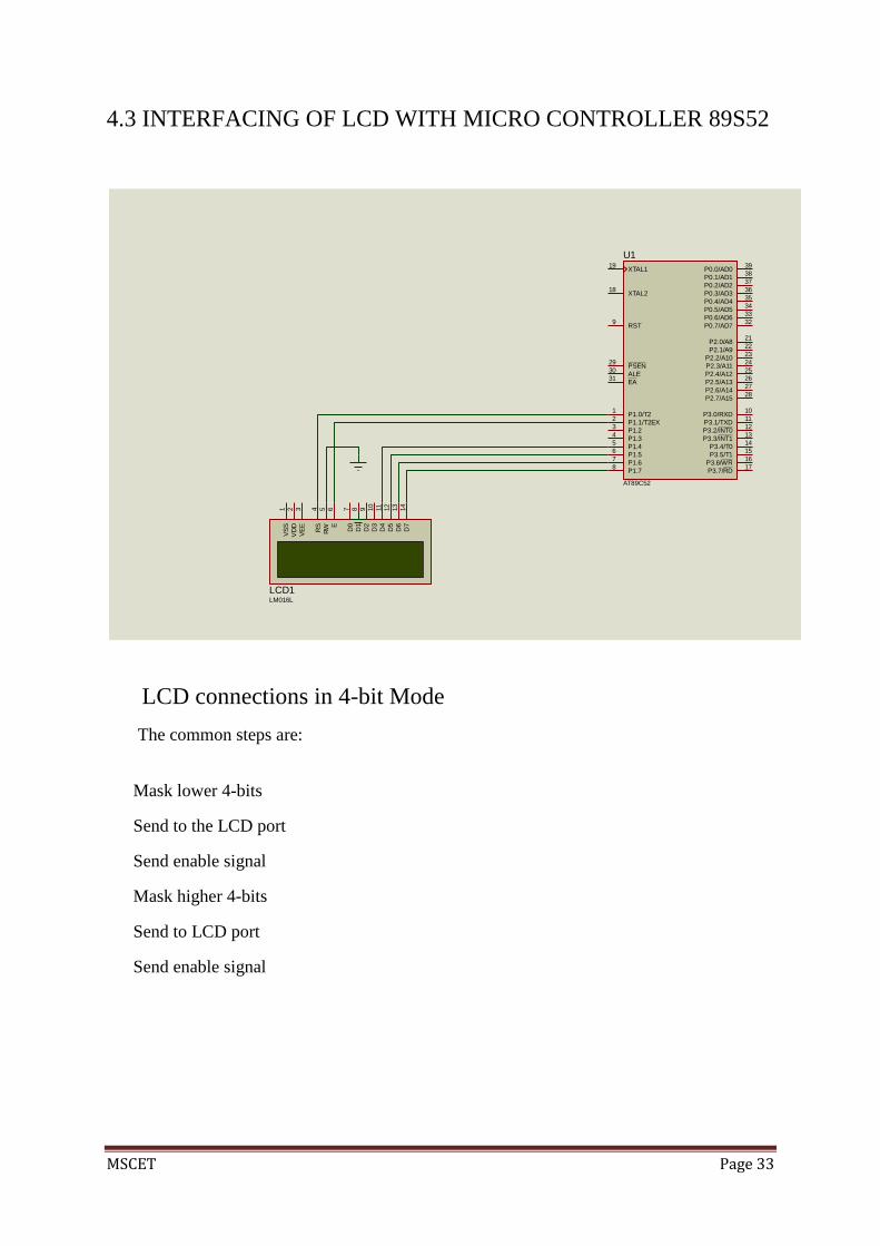
4.3 INTERFACING OF LCD WITH MICRO CONTROLLER 89S52
LCD connections in 4-bit Mode
The common steps are:
Mask lower 4-bits
Send to the LCD port
Send enable signal
Mask higher 4-bits
Send to LCD port
Send enable signal
XTAL218
XTAL119
ALE30
EA31
PSEN29
RST9
P0.0/AD039
P0.1/AD138
P0.2/AD237
P0.3/AD336
P0.4/AD435
P0.5/AD534
P0.6/AD633
P0.7/AD732
P1.0/T21
P1.1/T2EX2
P1.23
P1.34
P1.45
P1.56
P1.67
P1.78
P3.0/RXD10
P3.1/TXD11
P3.2/INT012
P3.3/INT113
P3.4/T014
P3.7/RD17
P3.6/WR16
P3.5/T115
P2.7/A1528
P2.0/A821
P2.1/A922
P2.2/A1023
P2.3/A1124
P2.4/A1225
P2.5/A1326
P2.6/A1427
U1
AT89C52
D7
14
D6
13
D5
12
D4
11
D3
10
D2
9D
18
D0
7
E6
RW
5R
S4
VS
S1
VD
D2
VE
E3
LCD1LM016L

MSCET Page 34
CHAPTER 5
HARDWARE IMPLEMENTATION

MSCET Page 35
5.1 FINAL WORKING MODEL:
Fig no :5.2 basic working model of solar bag.

MSCET Page 36
Fig no:- 5.3 Initial condition of working model after applying supply

MSCET Page 37
Fig no:5.3 condition of working model after reset

MSCET Page 38
CONCLUSION
From this project we observed that this bag is a portable electricity provider charging the
electronics devices. Also it is very cost effective and has many features.