sem and tem - personal webpages at ntnufolk.ntnu.no/jonathrg/fag/tfe4180/slides/jenkins 7-2 sem and...
TRANSCRIPT
1
TFE4180 Semiconductor Manufacturing Technology, TEM and SEM
SEM and TEMChapter 7.2 : Semiconductor Science by Tudor E. Jenkins
Saroj Kumar Patra,Department of Electronics and Telecommunication,
Norwegian University of Science and Technology ( NTNU )
2
Contents Why use electrons?
• De-Broglie Hypothesis• Electromagnetic lenses and Numerical Aperture
Transmission Electron Microscopy (TEM)• Structure• Use Mode• Practical complications
Scanning Electron Microscopy (SEM)• Structure• Use Mode
Scanning Transmission Electron Microscopy (STEM) Energy Dispersive X-ray Spectroscopy (EDS) Electron Energy Loss Spectroscopy (EELS)
TFE4180 Semiconductor Manufacturing Technology, TEM and SEM
3
Contents Why use electrons?
• De-Broglie Hypothesis• Electromagnetic lenses and Numerical Aperture
Transmission Electron Microscopy (TEM)• Structure• Use Mode• Practical complications
Scanning Electron Microscopy (SEM)• Structure• Use Mode
Scanning Transmission Electron Microscopy (STEM) Energy Dispersive X-ray Spectroscopy (EDS) Electron Energy Loss Spectroscopy (EELS)
TFE4180 Semiconductor Manufacturing Technology, TEM and SEM
4
Why use electrons?
TFE4180 Semiconductor Manufacturing Technology, TEM and SEM
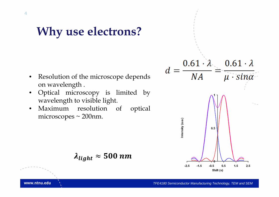
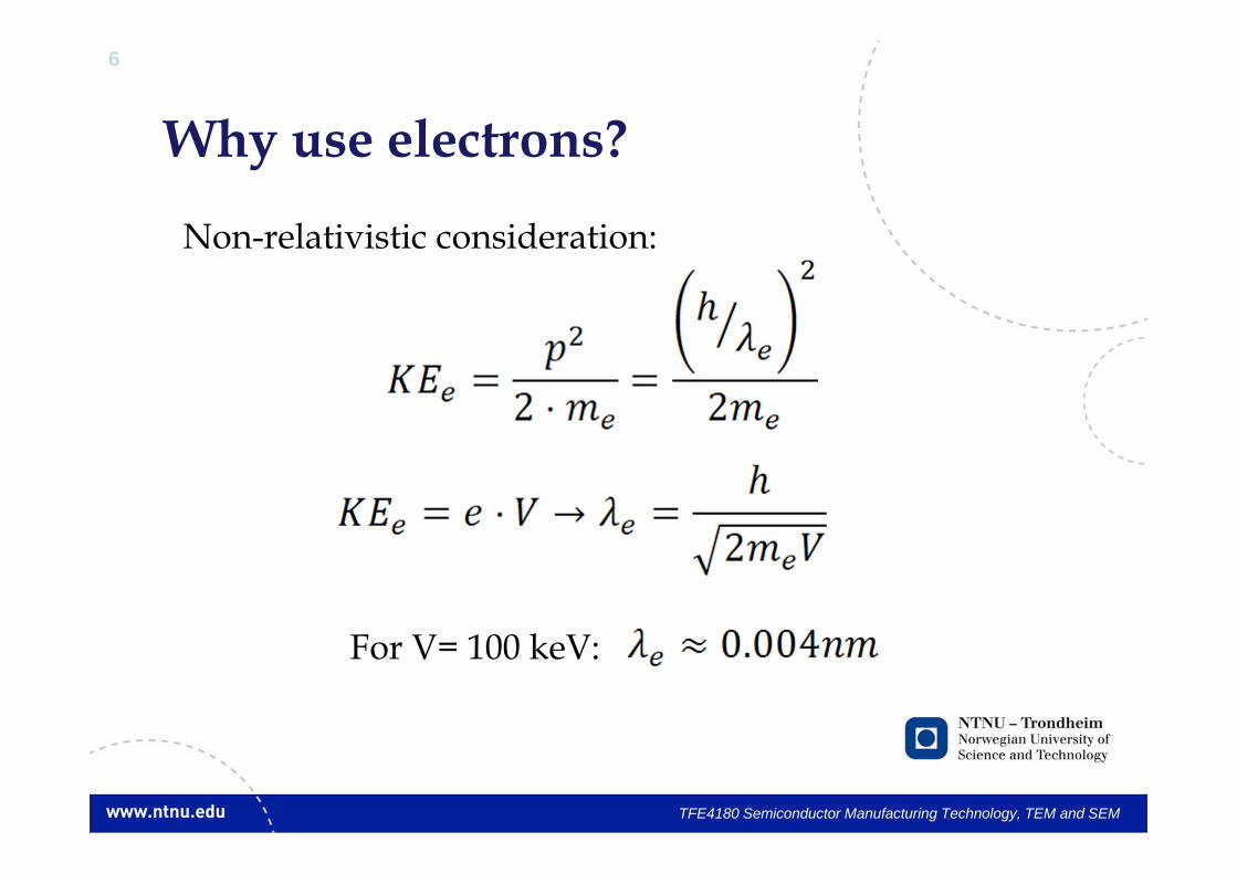
• Resolution of the microscope dependson wavelength .
• Optical microscopy is limited bywavelength to visible light.
• Maximum resolution of opticalmicroscopes ~ 200nm.
5
Why use electrons?
TFE4180 Semiconductor Manufacturing Technology, TEM and SEM
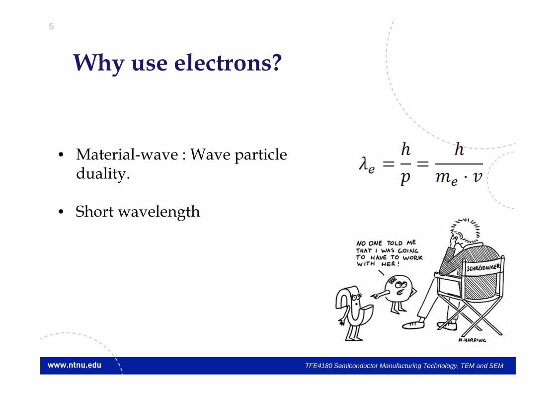
• Material-wave : Wave particle duality.
• Short wavelength
6
Why use electrons?
TFE4180 Semiconductor Manufacturing Technology, TEM and SEM
For V= 100 keV:
Non-relativistic consideration:
7
Electromagnetic Lenses
TFE4180 Semiconductor Manufacturing Technology, TEM and SEM
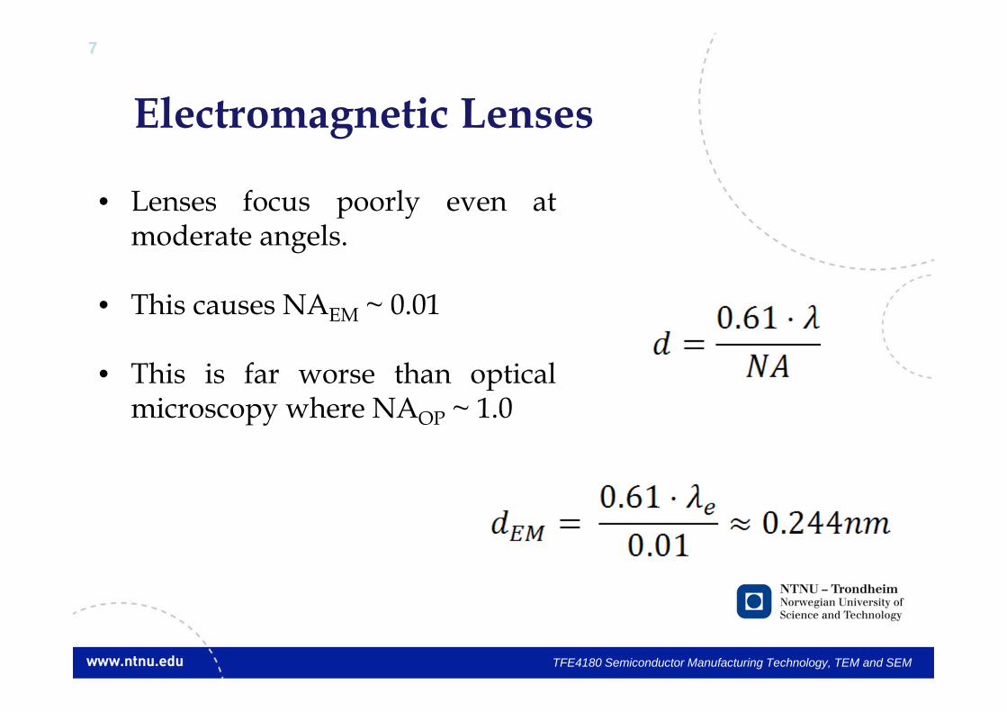
• Lenses focus poorly even atmoderate angels.
• This causes NAEM ~ 0.01
• This is far worse than opticalmicroscopy where NAOP ~ 1.0
8
Contents Why use electrons?
• De-Broglie Hypothesis• Electromagnetic lenses and Numerical Aperture
Transmission Electron Microscopy (TEM)• Structure• Use Mode• Practical complications
Scanning Electron Microscopy (SEM)• Structure• Use Mode
Scanning Transmission Electron Microscopy (STEM) Energy Dispersive X-ray Spectroscopy (EDS) Electron Energy Loss Spectroscopy (EELS)
TFE4180 Semiconductor Manufacturing Technology, TEM and SEM
9
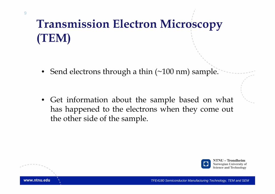
Transmission Electron Microscopy (TEM)
TFE4180 Semiconductor Manufacturing Technology, TEM and SEM
• Send electrons through a thin (~100 nm) sample.
• Get information about the sample based on whathas happened to the electrons when they come outthe other side of the sample.
10
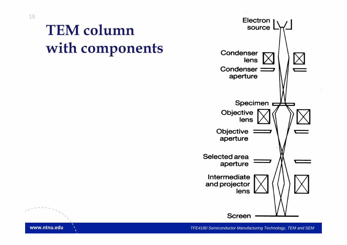
TEM column with components
TFE4180 Semiconductor Manufacturing Technology, TEM and SEM
11
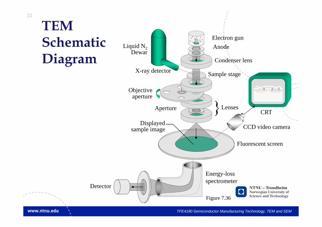
TEMSchematicDiagram
TFE4180 Semiconductor Manufacturing Technology, TEM and SEM
Energy-loss spectrometer
Aperture
Sample stage
Detector
CCD video camera
Fluorescent screen
CRT
Condenser lens
Anode
Lenses
Electron gun
X-ray detector
Objective aperture
Displayed sample image
Liquid N2Dewar
Figure 7.36
12
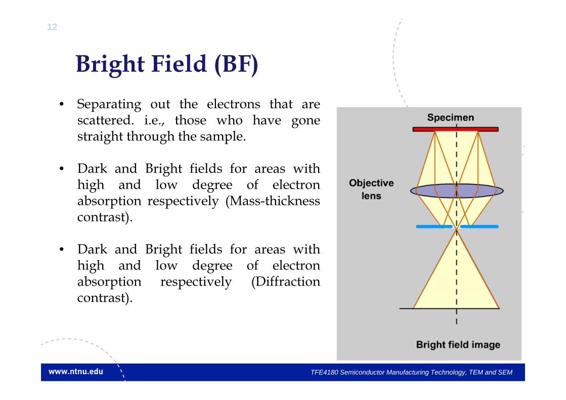
Bright Field (BF)
TFE4180 Semiconductor Manufacturing Technology, TEM and SEM
• Separating out the electrons that arescattered. i.e., those who have gonestraight through the sample.
• Dark and Bright fields for areas withhigh and low degree of electronabsorption respectively (Mass-thicknesscontrast).
• Dark and Bright fields for areas withhigh and low degree of electronabsorption respectively (Diffractioncontrast).
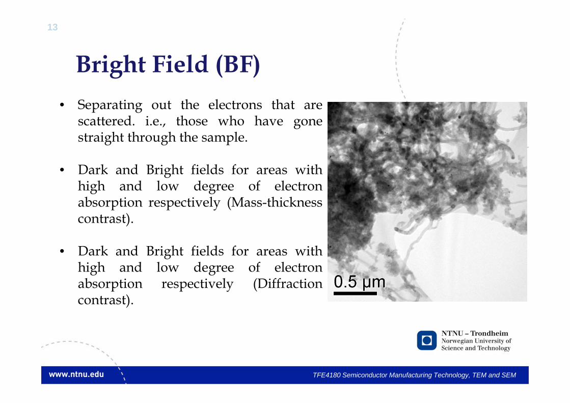
13
Bright Field (BF)
TFE4180 Semiconductor Manufacturing Technology, TEM and SEM
• Separating out the electrons that arescattered. i.e., those who have gonestraight through the sample.
• Dark and Bright fields for areas withhigh and low degree of electronabsorption respectively (Mass-thicknesscontrast).
• Dark and Bright fields for areas withhigh and low degree of electronabsorption respectively (Diffractioncontrast).
14
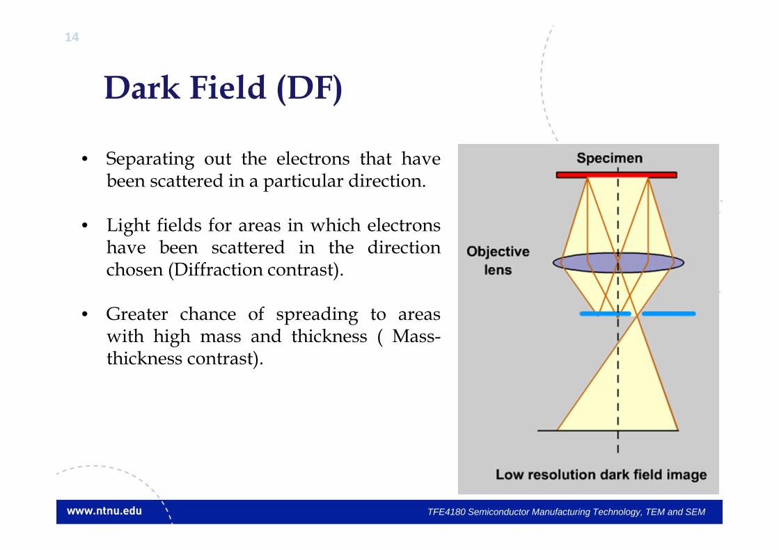
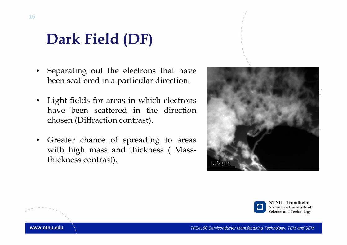
Dark Field (DF)
TFE4180 Semiconductor Manufacturing Technology, TEM and SEM
• Separating out the electrons that havebeen scattered in a particular direction.
• Light fields for areas in which electronshave been scattered in the directionchosen (Diffraction contrast).
• Greater chance of spreading to areaswith high mass and thickness ( Mass-thickness contrast).
15
Dark Field (DF)
TFE4180 Semiconductor Manufacturing Technology, TEM and SEM
• Separating out the electrons that havebeen scattered in a particular direction.
• Light fields for areas in which electronshave been scattered in the directionchosen (Diffraction contrast).
• Greater chance of spreading to areaswith high mass and thickness ( Mass-thickness contrast).
16
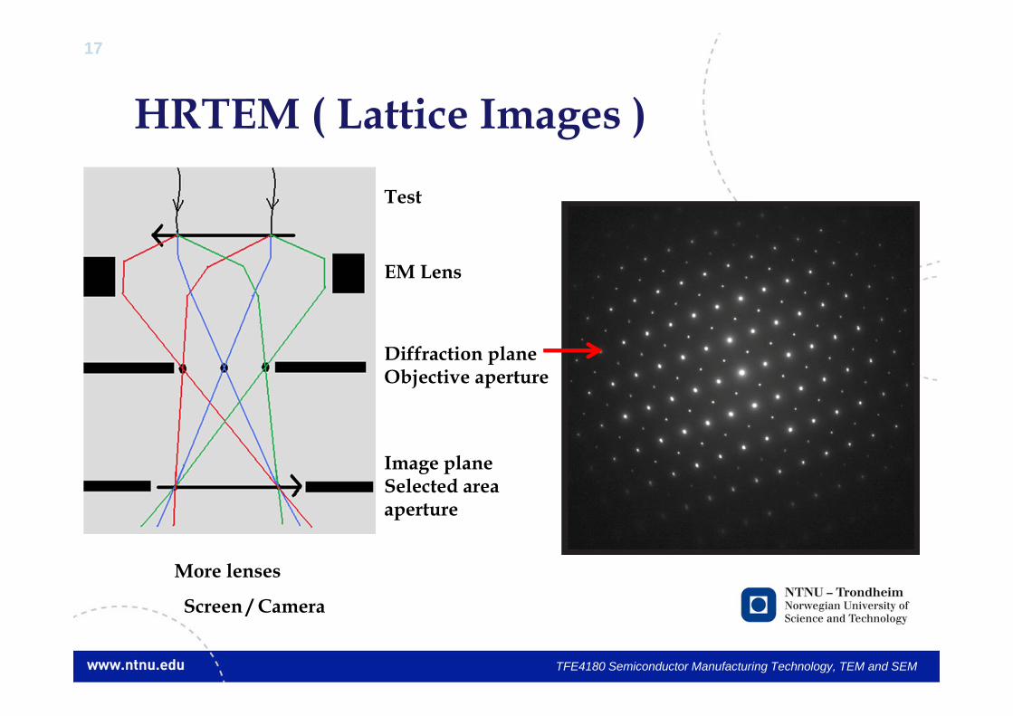
HRTEM ( Lattice Images )
TFE4180 Semiconductor Manufacturing Technology, TEM and SEM
• Why ? : To take the “image” of the crystal planes in thematerial.
• How ? : Setting out both the non-diffracted beam andone of the diffracted rays with lens aperture and letthem interfere in the image plane.
Lets go back a little…..
17
HRTEM ( Lattice Images )
TFE4180 Semiconductor Manufacturing Technology, TEM and SEM
Test
EM Lens
Diffraction planeObjective aperture
Image planeSelected area aperture
More lenses
Screen / Camera
18
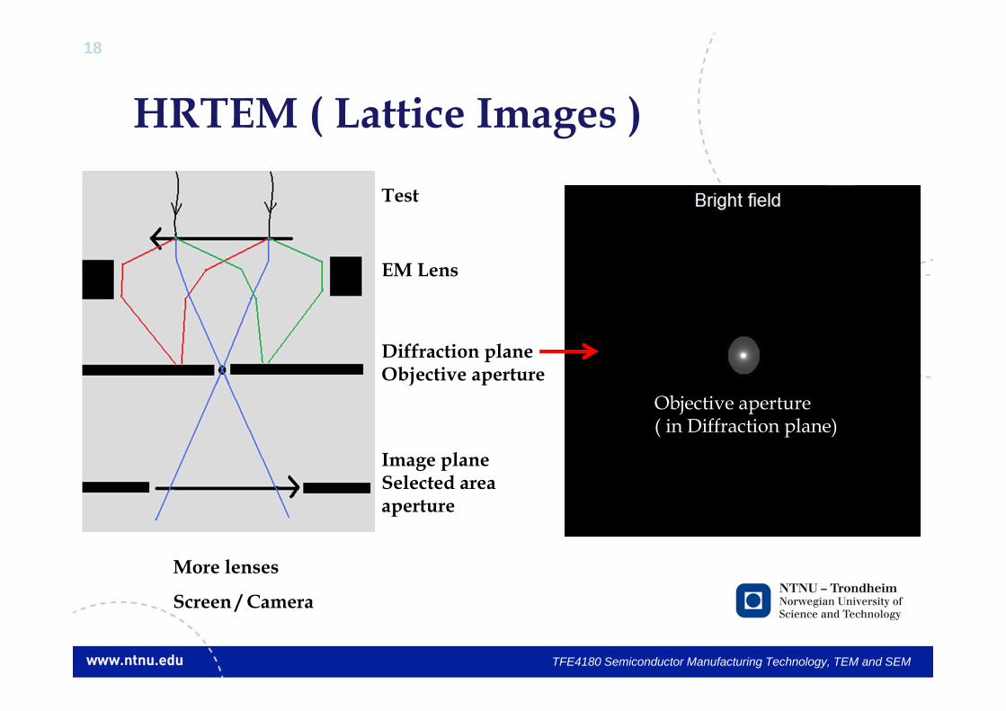
HRTEM ( Lattice Images )
TFE4180 Semiconductor Manufacturing Technology, TEM and SEM
Test
EM Lens
Diffraction planeObjective aperture
Image planeSelected area aperture
More lenses
Screen / Camera
Objective aperture ( in Diffraction plane)

19
HRTEM ( Lattice Images )
TFE4180 Semiconductor Manufacturing Technology, TEM and SEM
Test
EM Lens
Diffraction planeObjective aperture
Image planeSelected area aperture
More lenses
Screen / Camera
Objective aperture ( in Diffraction plane)
20
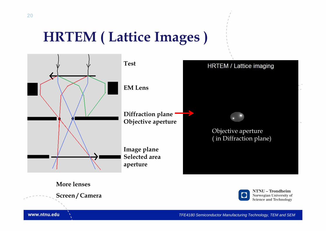
HRTEM ( Lattice Images )
TFE4180 Semiconductor Manufacturing Technology, TEM and SEM
Test
EM Lens
Diffraction planeObjective aperture
Image planeSelected area aperture
More lenses
Screen / Camera
Objective aperture ( in Diffraction plane)
21
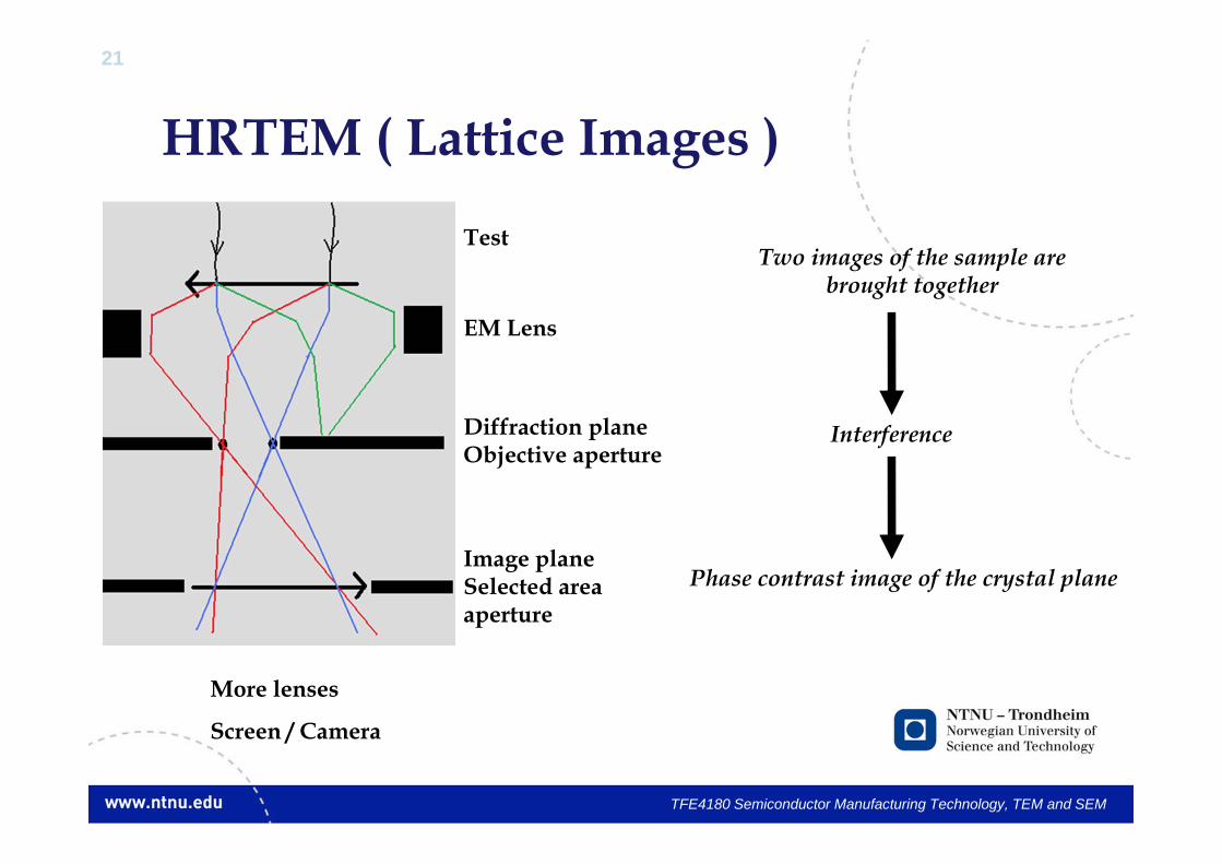
HRTEM ( Lattice Images )
TFE4180 Semiconductor Manufacturing Technology, TEM and SEM
Test
EM Lens
Diffraction planeObjective aperture
Image planeSelected area aperture
More lenses
Screen / Camera
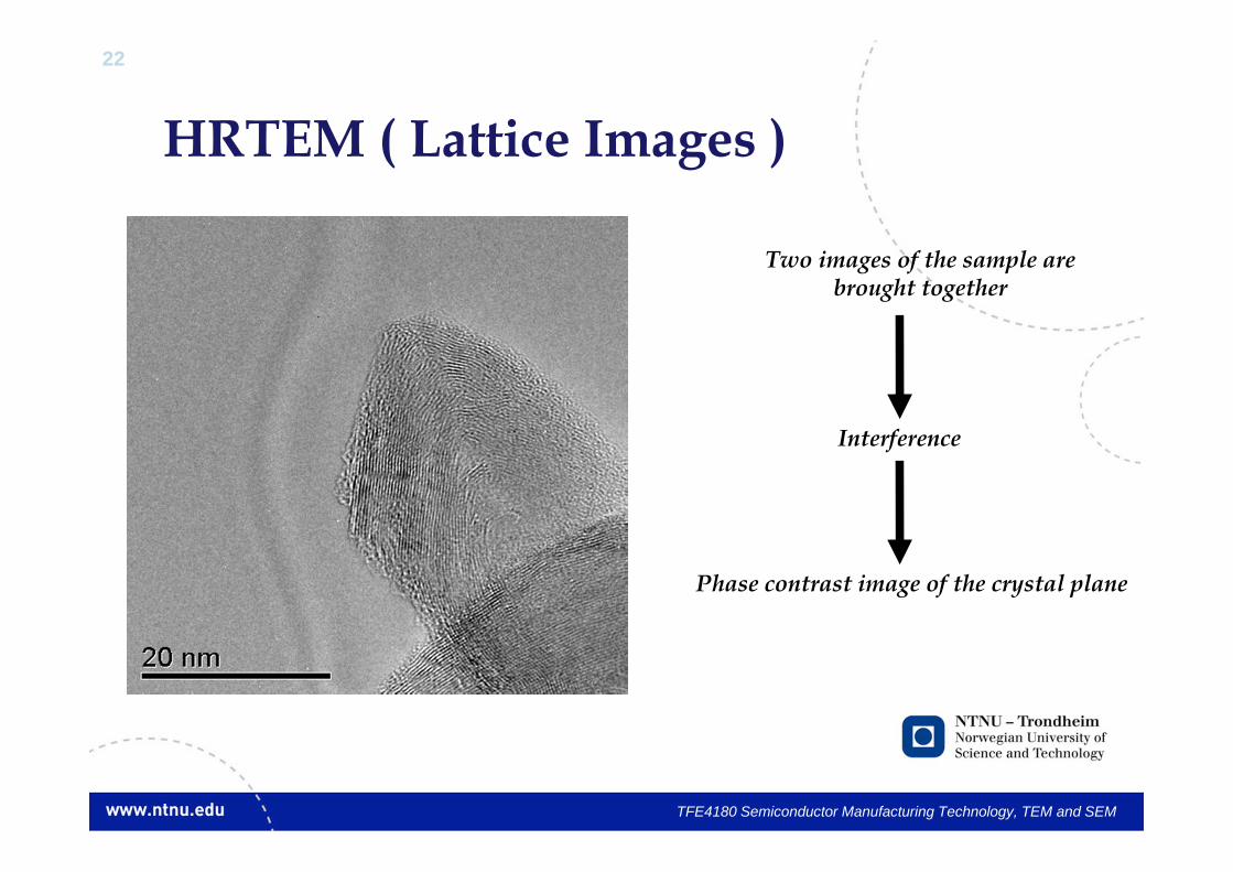
Two images of the sample are brought together
Interference
Phase contrast image of the crystal plane
22
HRTEM ( Lattice Images )
TFE4180 Semiconductor Manufacturing Technology, TEM and SEM
Two images of the sample are brought together
Interference
Phase contrast image of the crystal plane
23
Electron Diffraction
TFE4180 Semiconductor Manufacturing Technology, TEM and SEM
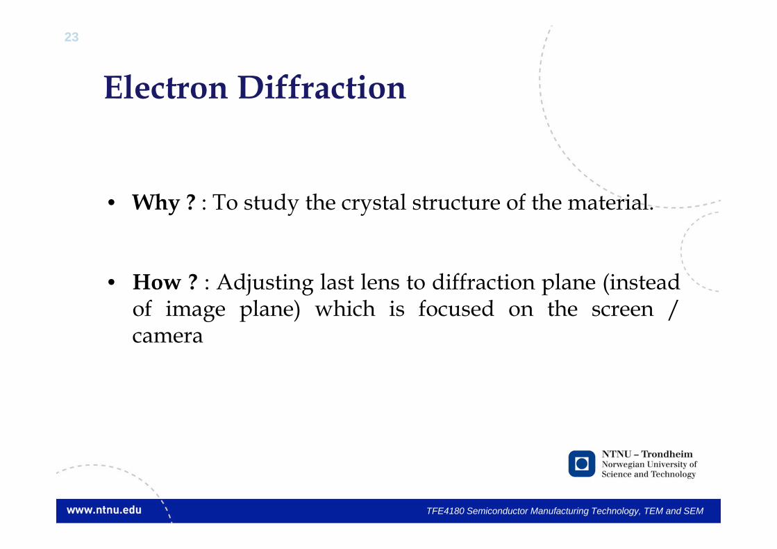
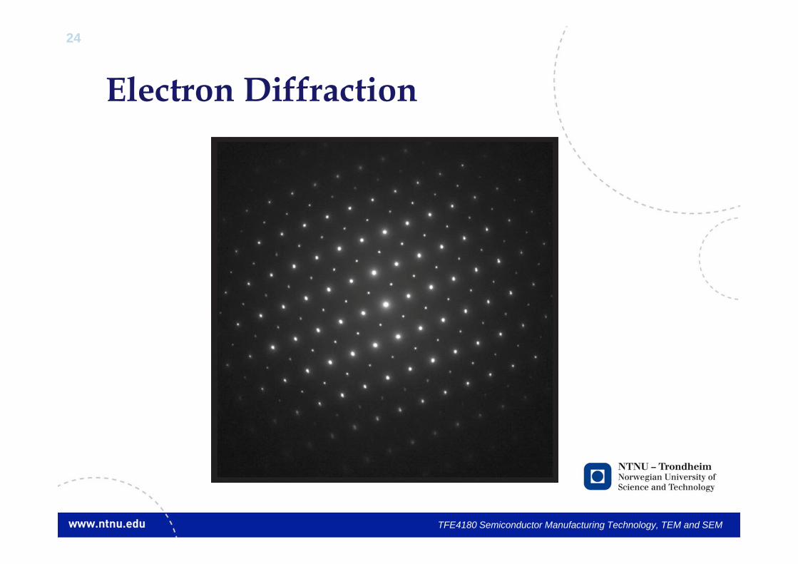
• Why ? : To study the crystal structure of the material.
• How ? : Adjusting last lens to diffraction plane (insteadof image plane) which is focused on the screen /camera
24
Electron Diffraction
TFE4180 Semiconductor Manufacturing Technology, TEM and SEM
25
Electron Diffraction
TFE4180 Semiconductor Manufacturing Technology, TEM and SEM
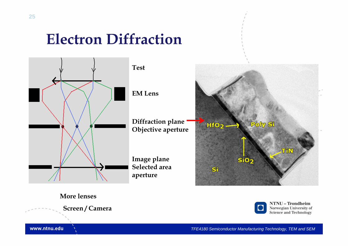
Test
EM Lens
Diffraction planeObjective aperture
Image planeSelected area aperture
More lenses
Screen / Camera
26
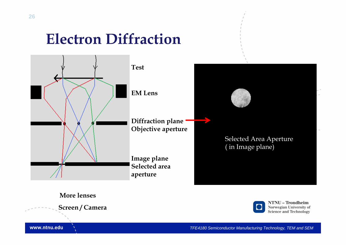
Electron Diffraction
TFE4180 Semiconductor Manufacturing Technology, TEM and SEM
Test
EM Lens
Diffraction planeObjective aperture
Image planeSelected area aperture
More lenses
Screen / Camera
Selected Area Aperture ( in Image plane)
27
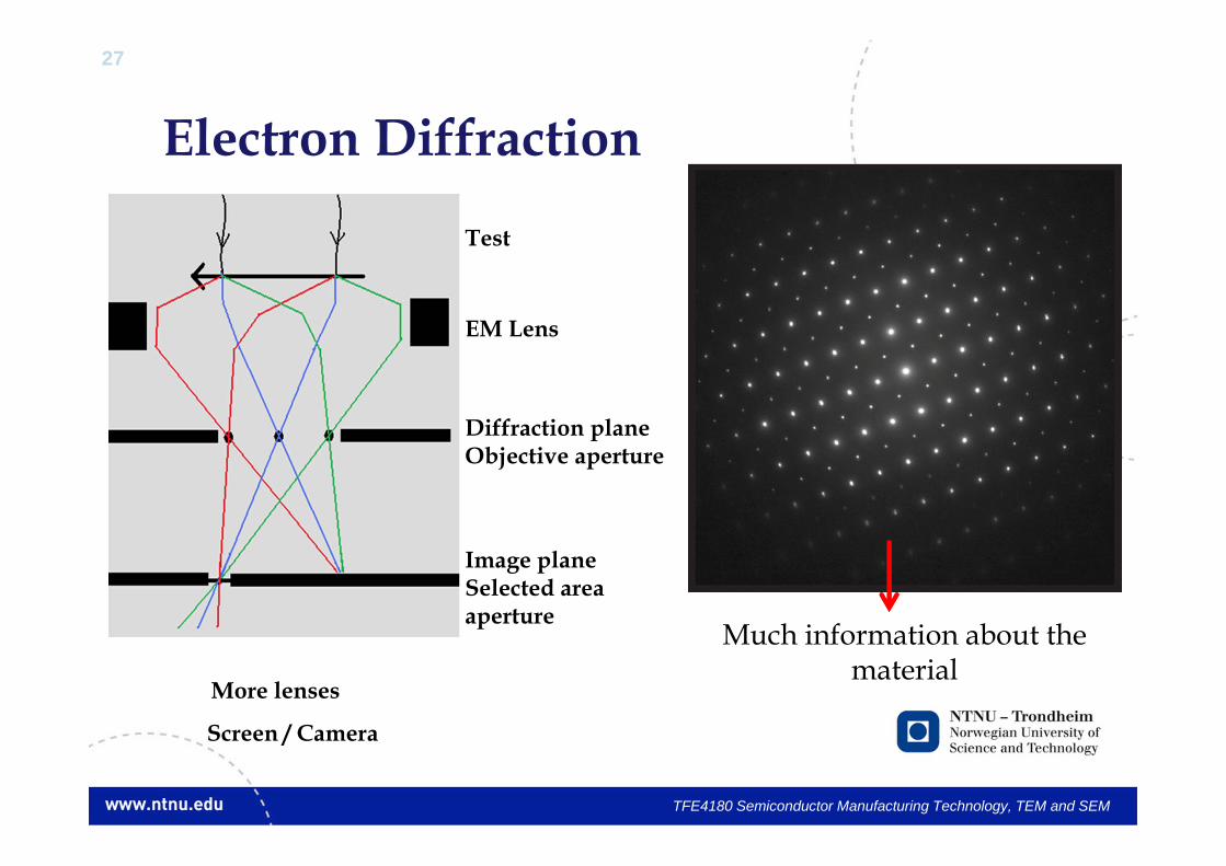
Electron Diffraction
TFE4180 Semiconductor Manufacturing Technology, TEM and SEM
Test
EM Lens
Diffraction planeObjective aperture
Image planeSelected area aperture
More lenses
Screen / Camera
Much information about the material

28
TEM Practical Complications
TFE4180 Semiconductor Manufacturing Technology, TEM and SEM
• Must have thin samples (e.g., ~ 100 nm) Difficult
Time consuming
Can change the sample
• Damage to the sample
• Narrow view
29
Contents Why use electrons?
• De-Broglie Hypothesis• Electromagnetic lenses and Numerical Aperture
Transmission Electron Microscopy (TEM)• Structure• Use Mode• Practical complications
Scanning Electron Microscopy (SEM)• Structure• Use Mode
Scanning Transmission Electron Microscopy (STEM) Energy Dispersive X-ray Spectroscopy (EDS) Electron Energy Loss Spectroscopy (EELS)
TFE4180 Semiconductor Manufacturing Technology, TEM and SEM
30
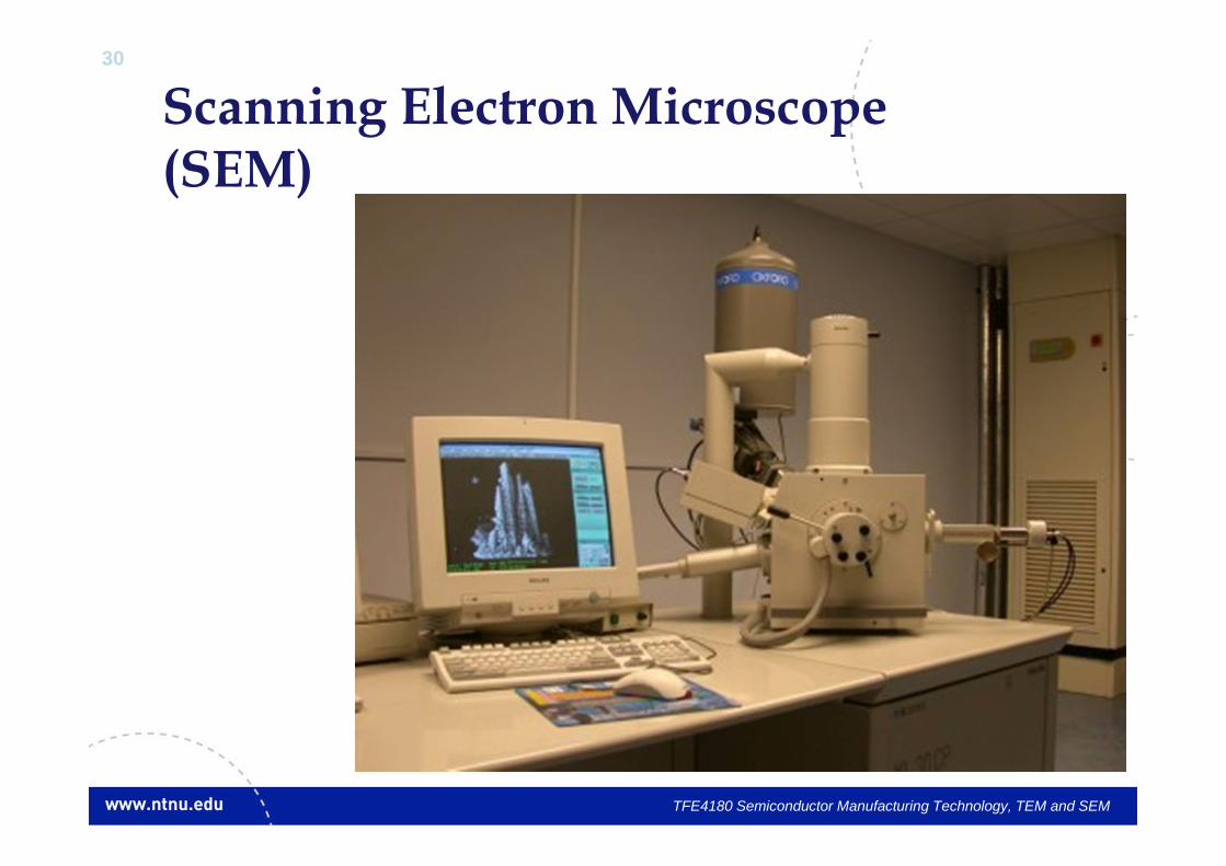
Scanning Electron Microscope (SEM)
TFE4180 Semiconductor Manufacturing Technology, TEM and SEM
31
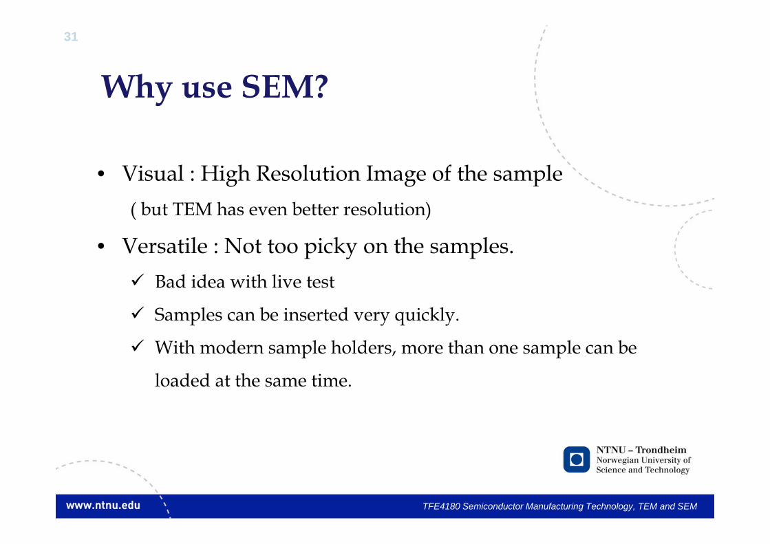
Why use SEM?
TFE4180 Semiconductor Manufacturing Technology, TEM and SEM
• Visual : High Resolution Image of the sample ( but TEM has even better resolution)
• Versatile : Not too picky on the samples. Bad idea with live test
Samples can be inserted very quickly.
With modern sample holders, more than one sample can be
loaded at the same time.
32
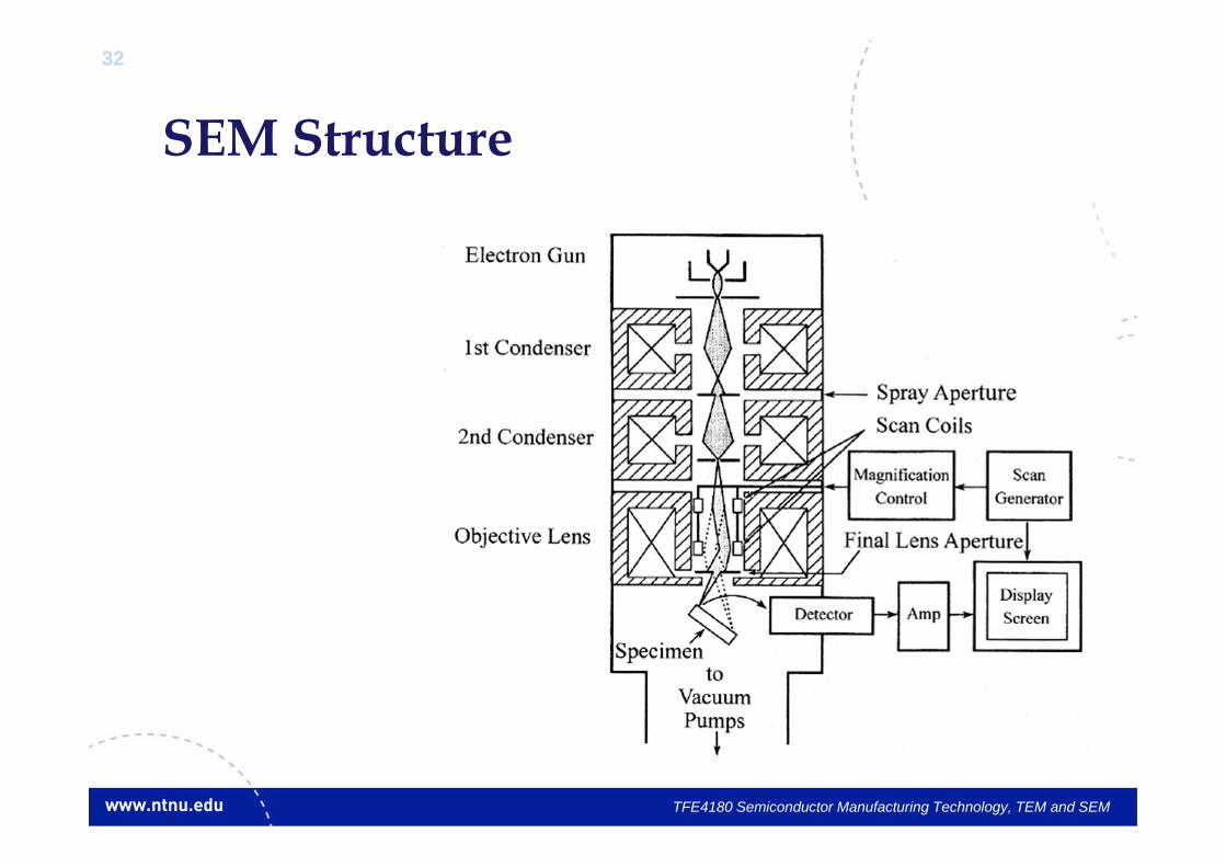
SEM Structure
TFE4180 Semiconductor Manufacturing Technology, TEM and SEM
33
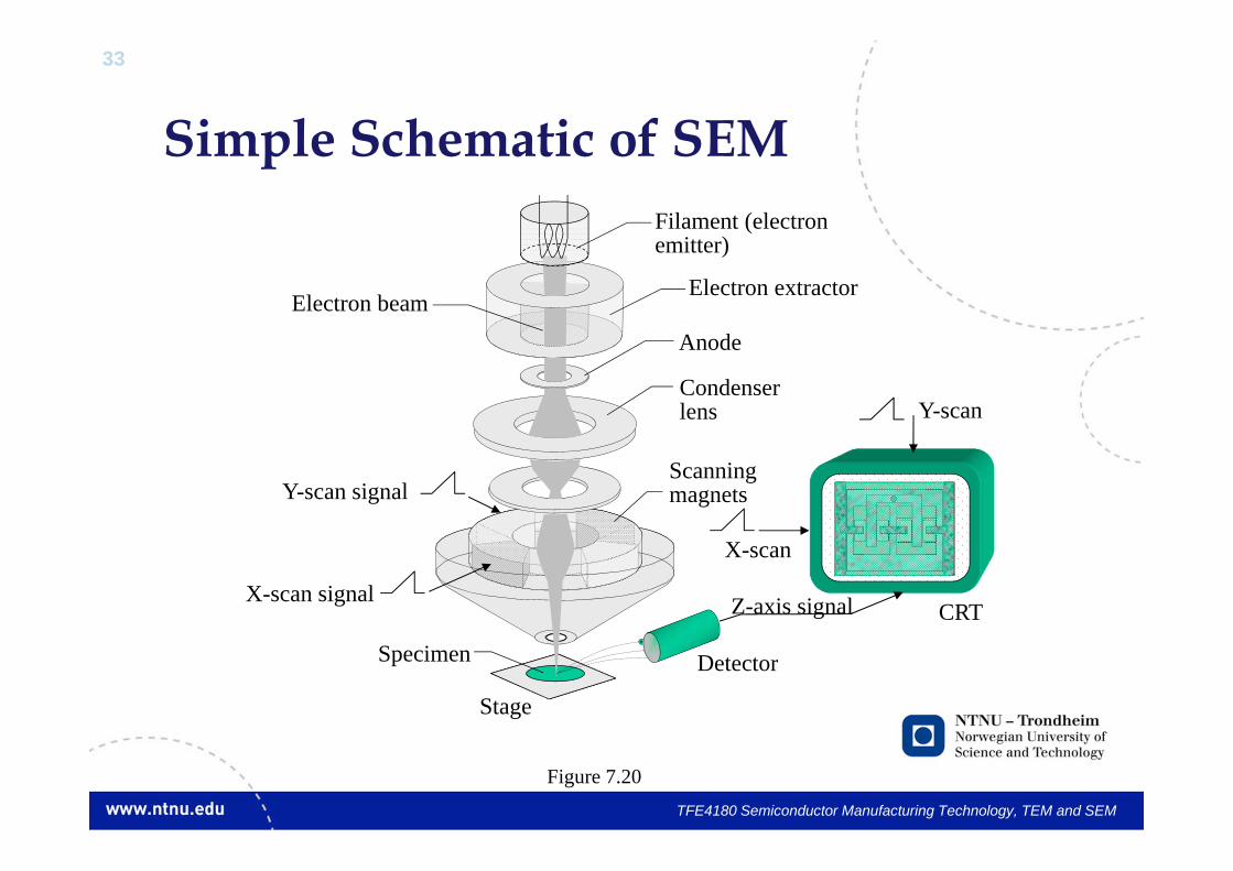
Simple Schematic of SEM
TFE4180 Semiconductor Manufacturing Technology, TEM and SEM
X-scan signal
Specimen
Scanning magnets
Stage
Detector
Y-scan signal
X-scan
Y-scan
Z-axis signal CRT
Condenser lens
Anode
Electron extractor
Filament (electron emitter)
Electron beam
Figure 7.20
34
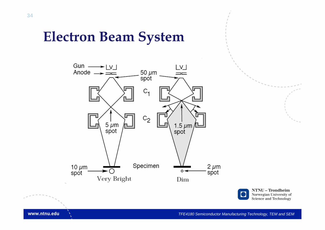
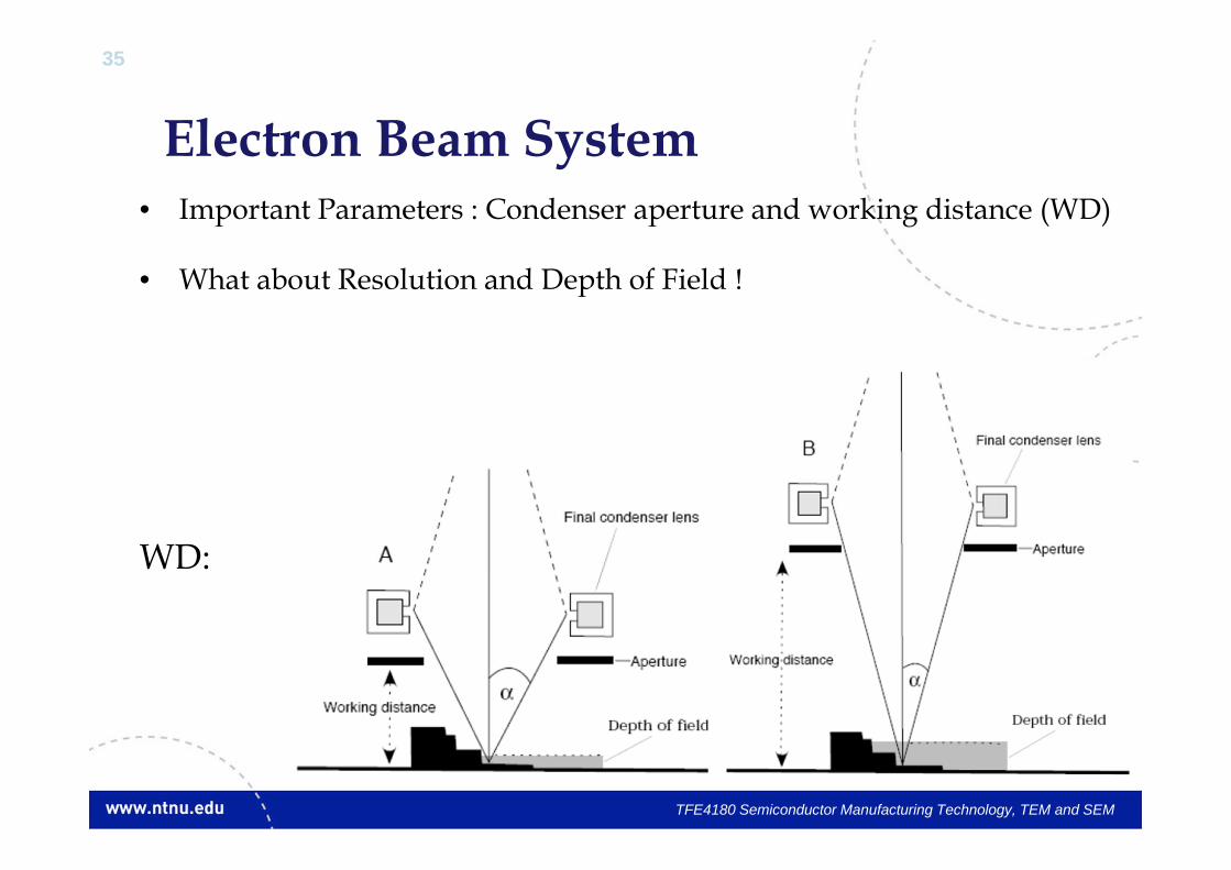
Electron Beam System
TFE4180 Semiconductor Manufacturing Technology, TEM and SEM
35
Electron Beam System
TFE4180 Semiconductor Manufacturing Technology, TEM and SEM
WD:
• Important Parameters : Condenser aperture and working distance (WD)
• What about Resolution and Depth of Field !
36
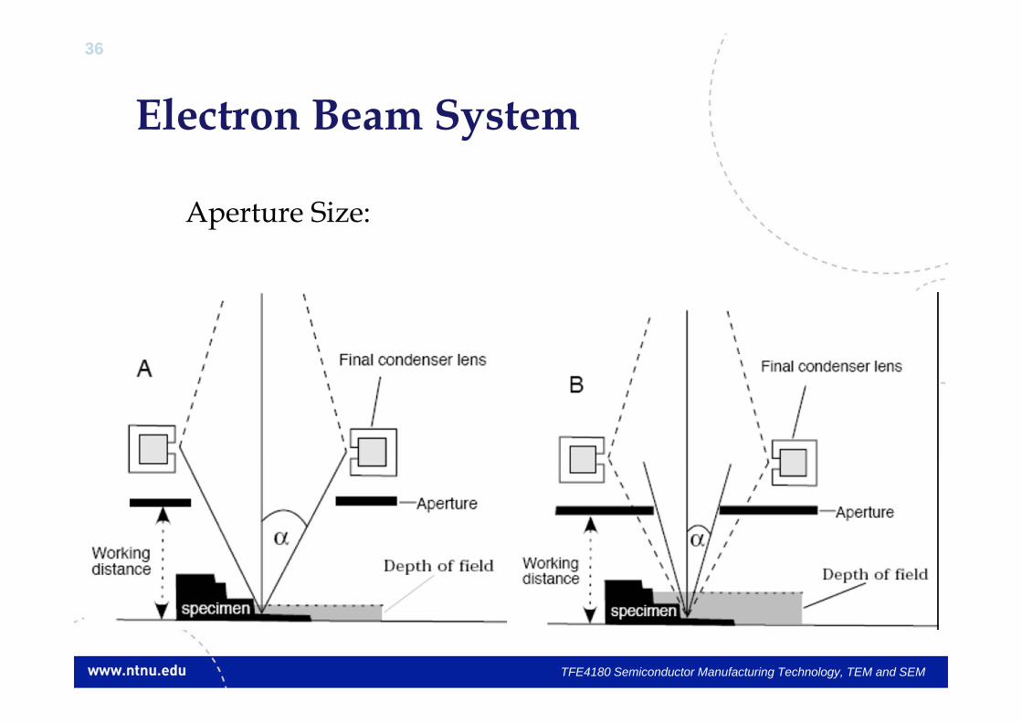
Electron Beam System
TFE4180 Semiconductor Manufacturing Technology, TEM and SEM
Aperture Size:
37
Electron Beam System
TFE4180 Semiconductor Manufacturing Technology, TEM and SEM
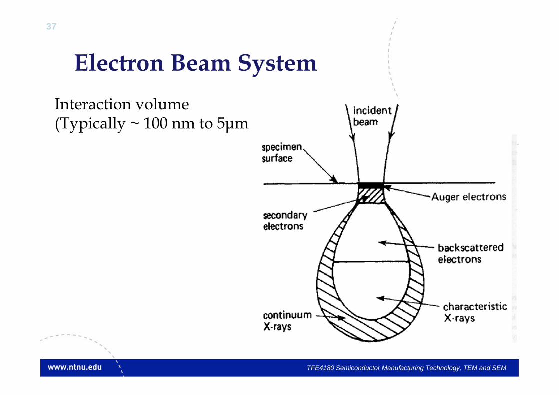
Interaction volume(Typically ~ 100 nm to 5μm
38
Secondary Electrons
TFE4180 Semiconductor Manufacturing Technology, TEM and SEM
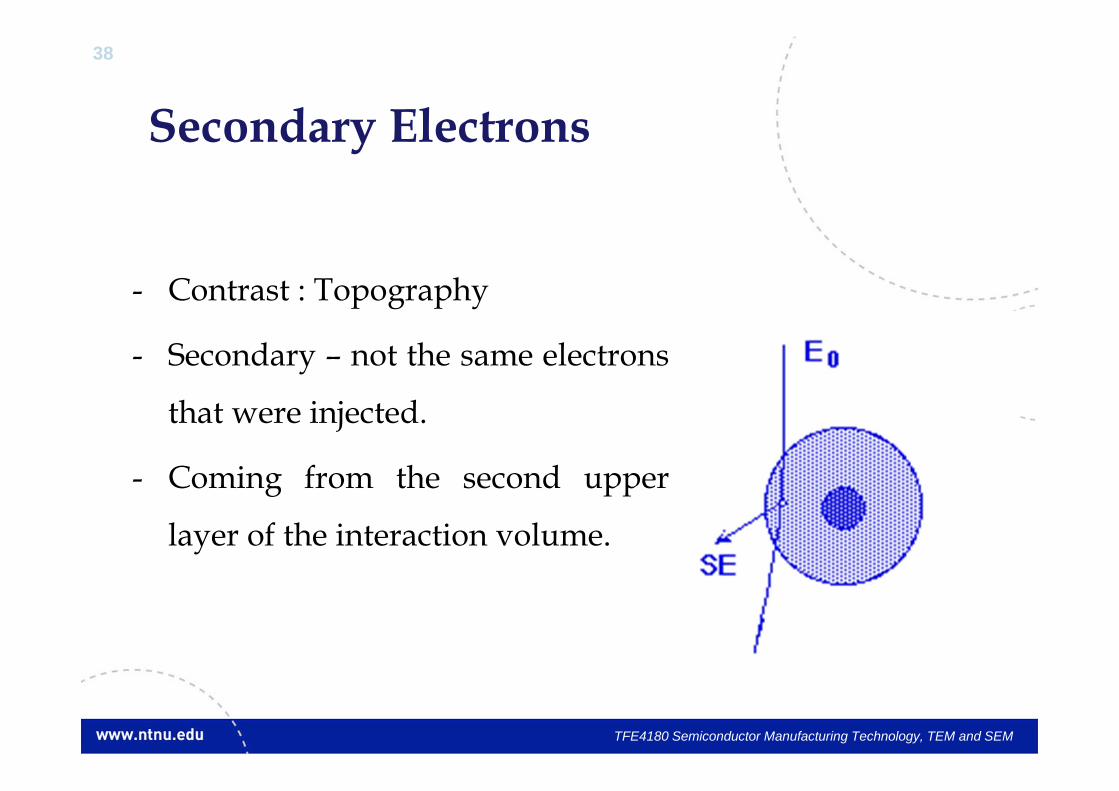
- Contrast : Topography
- Secondary – not the same electrons
that were injected.
- Coming from the second upper
layer of the interaction volume.

39
SEM Image
TFE4180 Semiconductor Manufacturing Technology, TEM and SEM
40
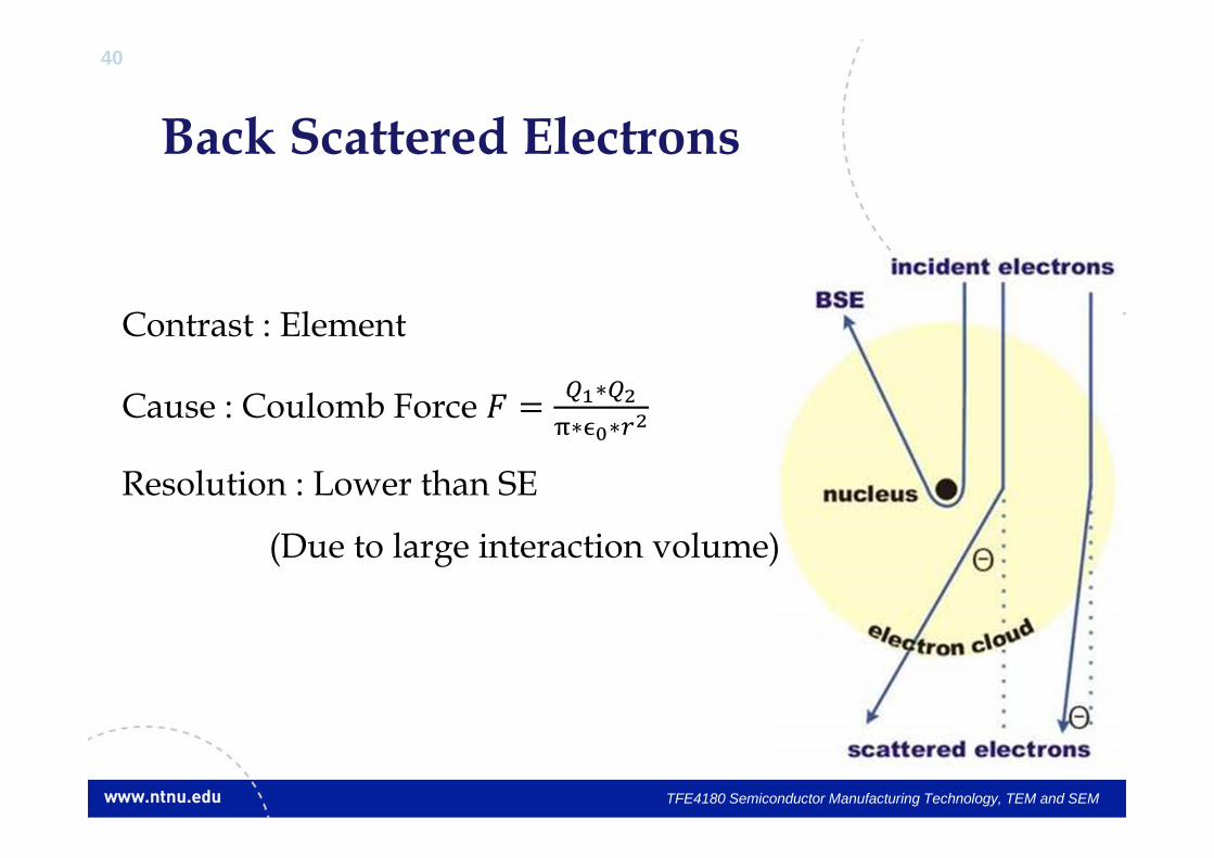
Back Scattered Electrons
TFE4180 Semiconductor Manufacturing Technology, TEM and SEM
Contrast : Element
Cause : Coulomb Force ∗∗ ∗
Resolution : Lower than SE
(Due to large interaction volume)
41
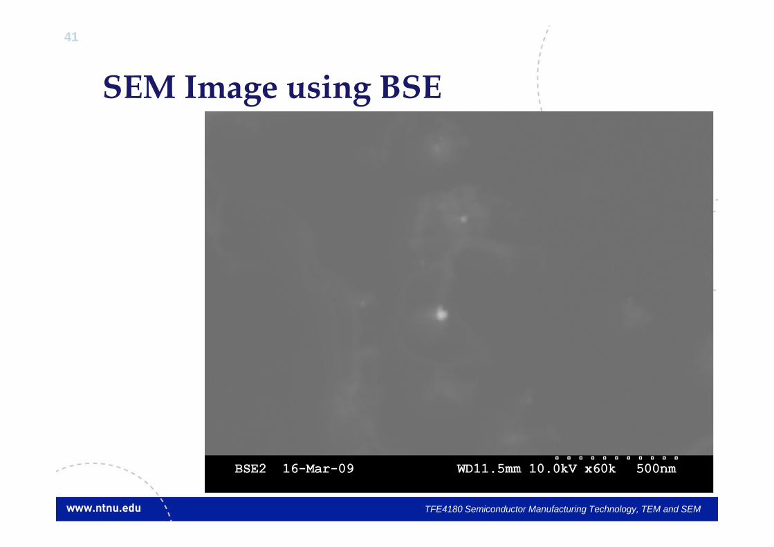
SEM Image using BSE
TFE4180 Semiconductor Manufacturing Technology, TEM and SEM
42
Contents Why use electrons?
• De-Broglie Hypothesis• Electromagnetic lenses and Numerical Aperture
Transmission Electron Microscopy (TEM)• Structure• Use Mode• Practical complications
Scanning Electron Microscopy (SEM)• Structure• Use Mode
Scanning Transmission Electron Microscopy (STEM) Energy Dispersive X-ray Spectroscopy (EDS) Electron Energy Loss Spectroscopy (EELS)
TFE4180 Semiconductor Manufacturing Technology, TEM and SEM
43
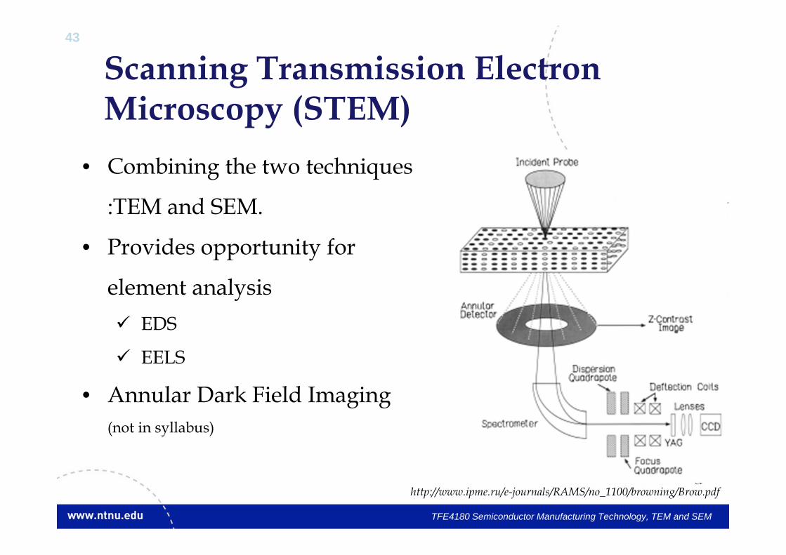
Scanning Transmission Electron Microscopy (STEM)
TFE4180 Semiconductor Manufacturing Technology, TEM and SEM
http://www.ipme.ru/e-journals/RAMS/no_1100/browning/Brow.pdf
• Combining the two techniques
:TEM and SEM.
• Provides opportunity for
element analysis EDS
EELS
• Annular Dark Field Imaging (not in syllabus)
44
Contents Why use electrons?
• De-Broglie Hypothesis• Electromagnetic lenses and Numerical Aperture
Transmission Electron Microscopy (TEM)• Structure• Use Mode• Practical complications
Scanning Electron Microscopy (SEM)• Structure• Use Mode
Scanning Transmission Electron Microscopy (STEM) Energy Dispersive X-ray Spectroscopy (EDS) Electron Energy Loss Spectroscopy (EELS)
TFE4180 Semiconductor Manufacturing Technology, TEM and SEM
45
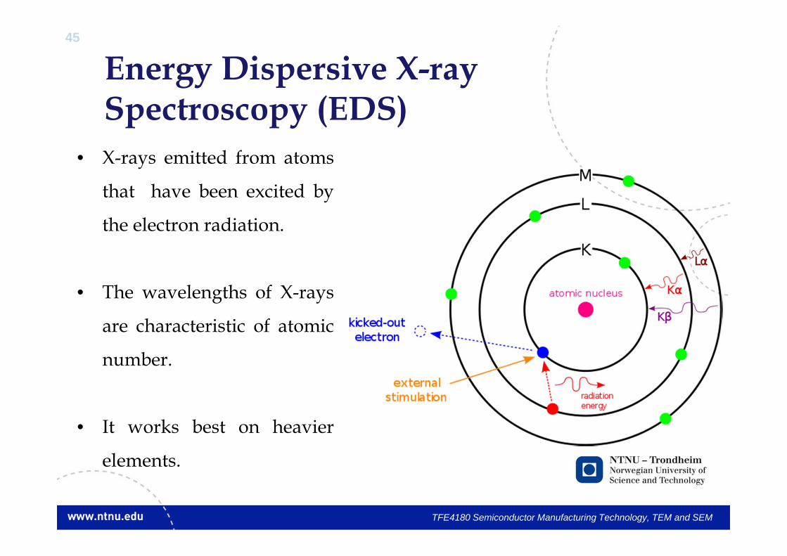
Energy Dispersive X-ray Spectroscopy (EDS)
TFE4180 Semiconductor Manufacturing Technology, TEM and SEM
• X-rays emitted from atoms
that have been excited by
the electron radiation.
• The wavelengths of X-rays
are characteristic of atomic
number.
• It works best on heavier
elements.
46
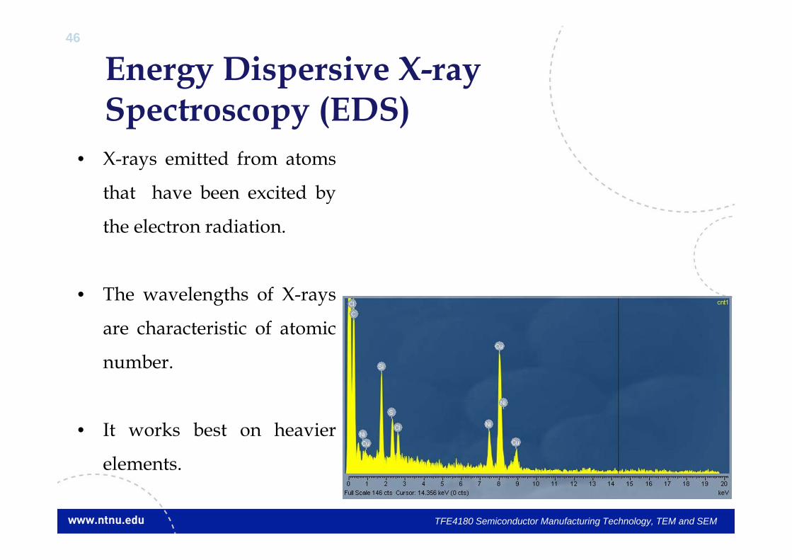
Energy Dispersive X-ray Spectroscopy (EDS)
TFE4180 Semiconductor Manufacturing Technology, TEM and SEM
• X-rays emitted from atoms
that have been excited by
the electron radiation.
• The wavelengths of X-rays
are characteristic of atomic
number.
• It works best on heavier
elements.

47
Contents Why use electrons?
• De-Broglie Hypothesis• Electromagnetic lenses and Numerical Aperture
Transmission Electron Microscopy (TEM)• Structure• Use Mode• Practical complications
Scanning Electron Microscopy (SEM)• Structure• Use Mode
Scanning Transmission Electron Microscopy (STEM) Energy Dispersive X-ray Spectroscopy (EDS) Electron Energy Loss Spectroscopy (EELS)
TFE4180 Semiconductor Manufacturing Technology, TEM and SEM
48
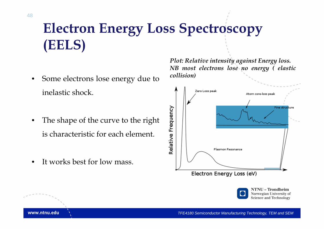
Electron Energy Loss Spectroscopy(EELS)
TFE4180 Semiconductor Manufacturing Technology, TEM and SEM
Plot: Relative intensity against Energy loss.NB most electrons lose no energy ( elasticcollision)• Some electrons lose energy due to
inelastic shock.
• The shape of the curve to the right
is characteristic for each element.
• It works best for low mass.

49
g{tÇ~ lÉâ
TFE4180 Semiconductor Manufacturing Technology, TEM and SEM