school of electrical and electronic engineering queen’s university belfast, n.ireland course tutor...
TRANSCRIPT

School of Electrical and Electronic EngineeringQueen’s University Belfast, N.Ireland
Course TutorDr R E Hurley
Semiconductor Device and Processing Technology
Northern Ireland Semiconductor Research Centre
School of Electrical & Electronic Engineering
The Queen’s University of Belfast
School of Electrical and Electronic EngineeringQueen’s University Belfast, N.Ireland
Semiconductor Device and Processing Technology
2. Silicon – properties and preparation

School of Electrical and Electronic EngineeringQueen’s University Belfast, N.Ireland
• Atomic no. 14. All levels filled to 3p.
• 3p has 2 electrons in levels with capacity 6.
• Hence Si shares with 4 nearest neighbours to satisfy unfilled 3p energy levels.

School of Electrical and Electronic EngineeringQueen’s University Belfast, N.Ireland
Silicon physical properties in the solid state
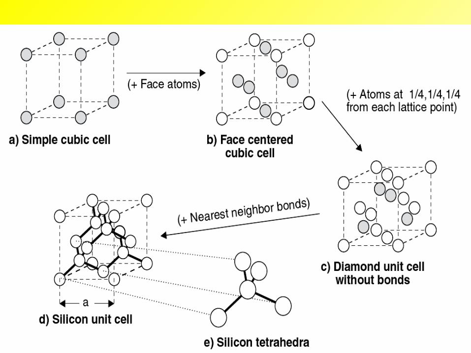
• Si is atomic number 14 and shares its outer electrons with the 4 nearest neighbour atoms forming covalent bonds
School of Electrical and Electronic EngineeringQueen’s University Belfast, N.Ireland
School of Electrical and Electronic EngineeringQueen’s University Belfast, N.Ireland
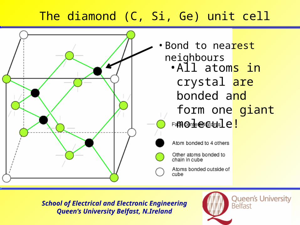
The diamond (C, Si, Ge) unit cell
• Bond to nearest neighbours
• All atoms in crystal are bonded and form one giant molecule!

School of Electrical and Electronic EngineeringQueen’s University Belfast, N.Ireland
• s2p2 electrons → sp3 → shared electron pairs → crystal formation
• s2p2 electrons → sp3 → shared electron pairs → crystal formation
Hybridization(the electron clouds
repel each other)

School of Electrical and Electronic EngineeringQueen’s University Belfast, N.Ireland
Silicon unit cell facts
• Lattice constant, a = 0.543 nm• Unit cell has 8 atoms• 1 atom corner, 3 atoms face, 4 atoms at ¼, ¼,
¼ lattice points• Unit cell volume is 1.6 × 10⁻²² cm3• 6.25 × 10²¹ unit cells/ cm3 = 5 × 10²²
atoms/cm3
• Nearest neighbour distance in 0.235 nm• Covalent radius is 0.118 nm → 27% packing
ratio

School of Electrical and Electronic EngineeringQueen’s University Belfast, N.Ireland
Silicon crystal for integrated circuits (ICs)
• (111) is the cheapest. Used for bipolars
• (110) is difficult to produce (experimental)
• (100) have best surface properties and used for MOST ICs.

School of Electrical and Electronic EngineeringQueen’s University Belfast, N.Ireland
Effect of (100), (110), (100) on surface properties
• (100) – 4 dangling surface bonds per unit cell
• (110) - 8 dangling (+parallel) bonds per unit cell
• (111) - 4 surface bonds per unit cell

School of Electrical and Electronic EngineeringQueen’s University Belfast, N.Ireland

School of Electrical and Electronic EngineeringQueen’s University Belfast, N.Ireland

School of Electrical and Electronic EngineeringQueen’s University Belfast, N.Ireland
• Allowed energy levels of 1 atom overlap and form bands when atoms form solid
• The outer 2 levels → valence and conduction band
• At 0 degrees Kelvin, conduction band is empty, valence band is full.
• Forbidden energy gap exists
Band structure of semiconductor

School of Electrical and Electronic EngineeringQueen’s University Belfast, N.Ireland
Silicon band structure at 3000K

School of Electrical and Electronic EngineeringQueen’s University Belfast, N.Ireland
Silicon band structure
• Semiconductors. Eg = 0.1 - 2.0 eV
• Insulators. Eg = several eV
• Conductors. Overlapping valence and conduction bands
For silicon, Eg (T) is given by
T is in 0K and 1.17 = Eg for Si at 0 0K.

School of Electrical and Electronic EngineeringQueen’s University Belfast, N.Ireland
• Silicon energy gap v. Temperature
School of Electrical and Electronic EngineeringQueen’s University Belfast, N.Ireland
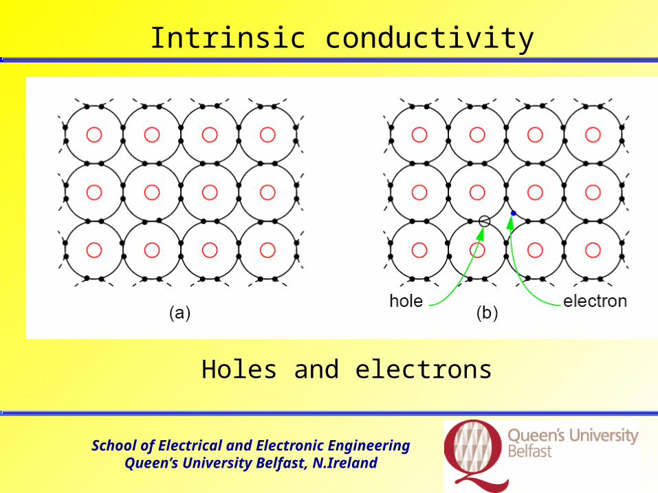
Intrinsic conductivity
Holes and electrons

School of Electrical and Electronic EngineeringQueen’s University Belfast, N.Ireland
• Electrons excited by thermal energy jump to conduction band and become mobile intrinsic carriers with density, ni :
k is Boltzmann’s constant
Intrinsic conductivity

School of Electrical and Electronic EngineeringQueen’s University Belfast, N.Ireland
Si intrinsic carrier concentration v. temperature

School of Electrical and Electronic EngineeringQueen’s University Belfast, N.Ireland
Doping silicon
• Group III → excess +ve carriers = holes = p-type
• Group V → excess –ve carriers = electrons = n-type
(Excess = excess of intrinsic concentration)
• Carriers can be majority or minority

School of Electrical and Electronic EngineeringQueen’s University Belfast, N.Ireland
School of Electrical and Electronic EngineeringQueen’s University Belfast, N.Ireland
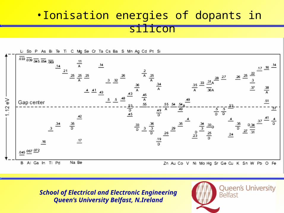
• Ionisation energies of dopants in silicon

School of Electrical and Electronic EngineeringQueen’s University Belfast, N.Ireland
Law of Mass Action
• In equilibrium:
Majority carrier density x Minority carrier density = constant for material and temperature
i.e. nh x ne = constant = ni2
ni = 1.4 x 1010 cm3 for silicon
Why?Generation rate is constant, f(T)Recombination rate is f(nh x ne, T)

School of Electrical and Electronic EngineeringQueen’s University Belfast, N.Ireland
Mobility
• Average velocity of carriers = carrier drift velocity, vd = E, where µ is the mobility = qτ/m*, E is the field.
(τ is meant time between scattering collisions, m* is effective mass)
• This is not valid at very high fields when scattering processes are non-uniform
School of Electrical and Electronic EngineeringQueen’s University Belfast, N.Ireland
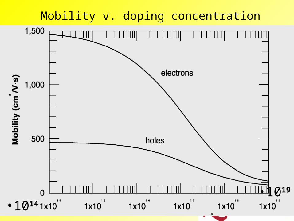
Mobility v. doping concentration
• 1019
• 1014

School of Electrical and Electronic EngineeringQueen’s University Belfast, N.Ireland
Resistivity
Standard well-known formula
For a doped semiconductor, n is carrier concentration

School of Electrical and Electronic EngineeringQueen’s University Belfast, N.Ireland
• Resistivity of silicon v. impurity concentration at 300K.
• 1021
• 1011
• 10-3
• 105
School of Electrical and Electronic EngineeringQueen’s University Belfast, N.Ireland
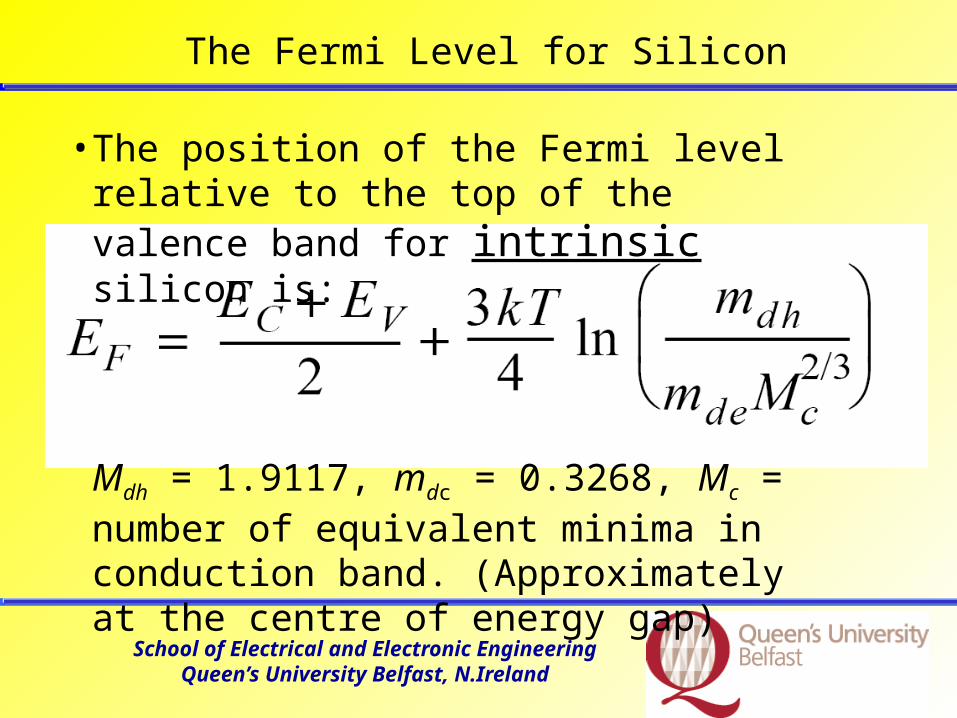
The Fermi Level for Silicon
• The position of the Fermi level relative to the top of the valence band for intrinsic silicon is:
Mdh = 1.9117, mdc = 0.3268, Mc = number of equivalent minima in conduction band. (Approximately at the centre of energy gap)

School of Electrical and Electronic EngineeringQueen’s University Belfast, N.Ireland
Fermi Level for extrinsic silicon
n or p >> ni,
Ei is the Fermi level for intrinsic silicon

School of Electrical and Electronic EngineeringQueen’s University Belfast, N.Ireland
• Fermi level v. temperature and doping

School of Electrical and Electronic EngineeringQueen’s University Belfast, N.Ireland
Defects in crystals
• In a crystal point defect concentration depends on thermal fluctuations and vapour pressure
• In silicon only thermal fluctuations important
• Defects will affect electronic properties
• Defect concentration depends on energy of formation and equilibrium temperature.
• Processes can produce defects and affect performance

School of Electrical and Electronic EngineeringQueen’s University Belfast, N.Ireland
Vacancy defects in silicon

School of Electrical and Electronic EngineeringQueen’s University Belfast, N.Ireland
Ways to form defects in silicon• In silicon unit cell there are 5 interstitial positions(½, ½, ½,),(¼, ¼, ¼),(¼,¾, ¼), and (¾, ¾, ¼)
3 ways to make point defects:
1. Schottky defect – silicon atom jumps to interstitial position and diffuses to surface, leaving vacancy.
2. Frenkel defect – silicon atom jumps to an interstitial, creating vacancy/interstitial pair.
3. Surface generation – surface atoms move to interstitial sites within lattice.

School of Electrical and Electronic EngineeringQueen’s University Belfast, N.Ireland
surface

School of Electrical and Electronic EngineeringQueen’s University Belfast, N.Ireland
No. of Frenkel defects per unit volume
School of Electrical and Electronic EngineeringQueen’s University Belfast, N.Ireland
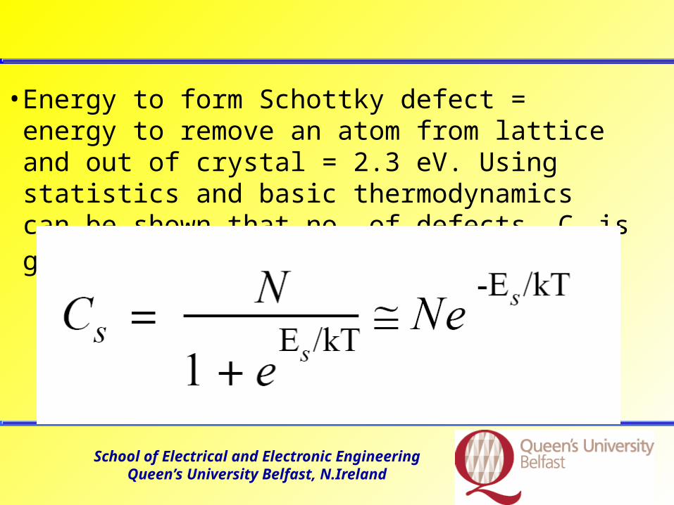
• Energy to form Schottky defect = energy to remove an atom from lattice and out of crystal = 2.3 eV. Using statistics and basic thermodynamics can be shown that no. of defects, Cs is given by: (N = atoms/cm3)
School of Electrical and Electronic EngineeringQueen’s University Belfast, N.Ireland
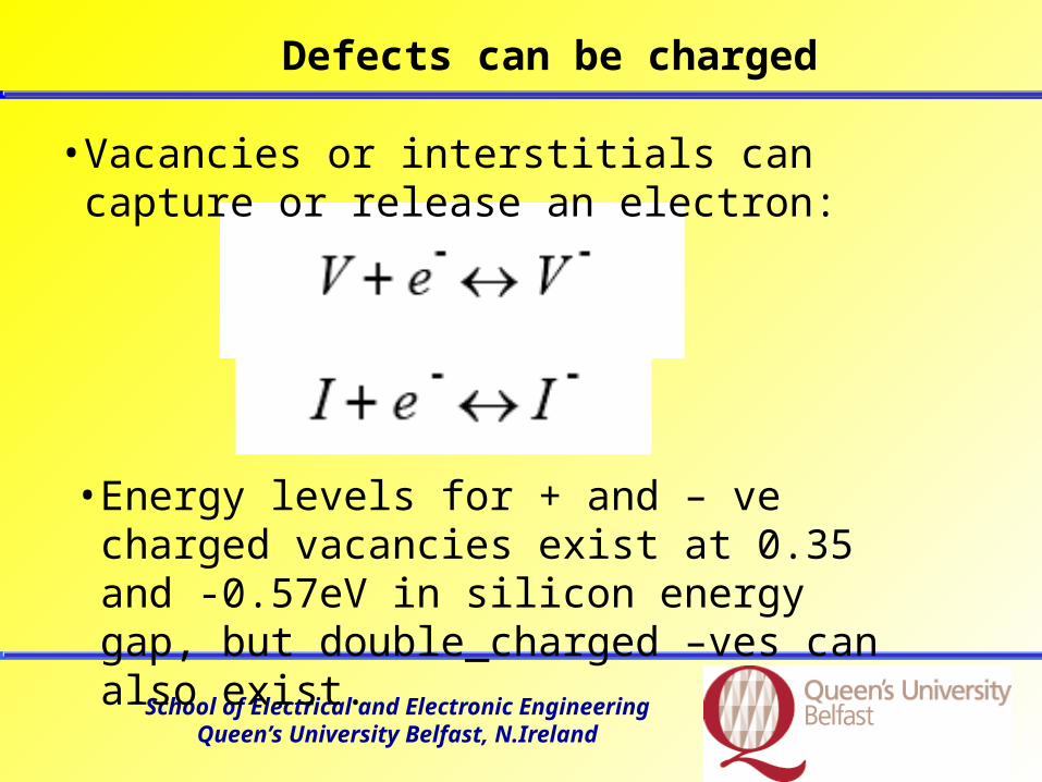
Defects can be charged
• Vacancies or interstitials can capture or release an electron:
• Energy levels for + and – ve charged vacancies exist at 0.35 and -0.57eV in silicon energy gap, but double_charged –ves can also exist.

School of Electrical and Electronic EngineeringQueen’s University Belfast, N.Ireland
Interstitial defects in silicon

School of Electrical and Electronic EngineeringQueen’s University Belfast, N.Ireland
• Processes causing defects:
• Thermal oxidation
• Thermal nitriding
• Ion implantation
• Exposure to radiation
Effect of silicon processing

School of Electrical and Electronic EngineeringQueen’s University Belfast, N.Ireland
Extended defects
Silicon processing may produce extended defects:
1. Dislocations
2. Twinning
3. Stacking faults

School of Electrical and Electronic EngineeringQueen’s University Belfast, N.Ireland
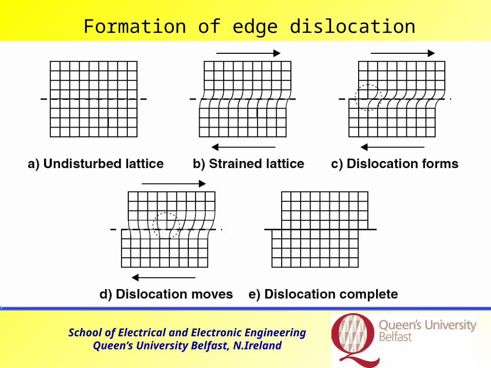
Dislocations in silicon
• Strain, a distortion of the crystal lattice is produced by stress. Sources of stress are:
1. Mechanical forces (high temperatures2. High dopant levels (dopants with size
mismatch to silicon)3. Thermal gradients:Thermal gradient strain, S = α Y ΔTα = coefficient of expansion, Y = Youngs Modulus,
ΔT is temperature difference between centre and edge of wafer.
If Stress > yield strength of silicon → dislocation
School of Electrical and Electronic EngineeringQueen’s University Belfast, N.Ireland
Formation of edge dislocation

School of Electrical and Electronic EngineeringQueen’s University Belfast, N.Ireland
Twinning (2 regions at differing orientations.)
Usually means many dislocations, micro-twinning can be produced by ion implantation
School of Electrical and Electronic EngineeringQueen’s University Belfast, N.Ireland
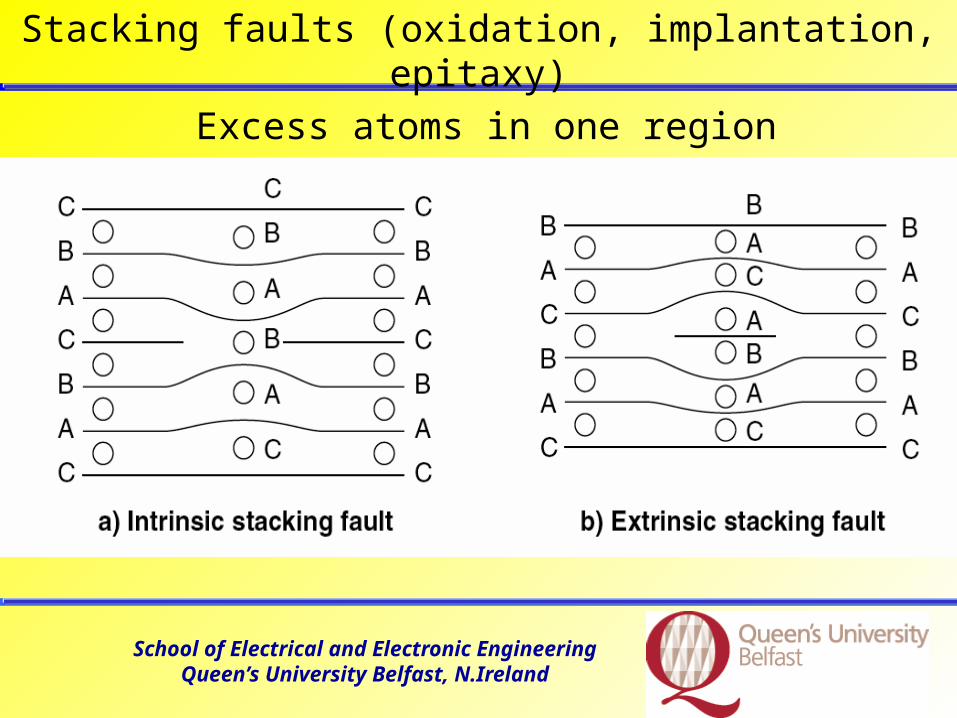
Stacking faults (oxidation, implantation, epitaxy)
Excess atoms in one region

School of Electrical and Electronic EngineeringQueen’s University Belfast, N.Ireland
Production of electronic grade polysilicon from SiO2
Arc furnace with coal or wood reduces SiO2 making 98% pure solid silicon.
Si powdered with HCl in fluid bed to form SiHCl3 .
The process starts with sand from Australian beaches

School of Electrical and Electronic EngineeringQueen’s University Belfast, N.Ireland
Reduced with high purity hydrogen to yield high purity silicon..
Then distilled to high purity.
This is one large polycrystal
Making silicon

School of Electrical and Electronic EngineeringQueen’s University Belfast, N.Ireland
Impurities in silicon
School of Electrical and Electronic EngineeringQueen’s University Belfast, N.Ireland
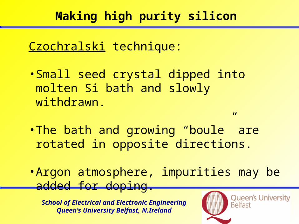
Making high purity silicon
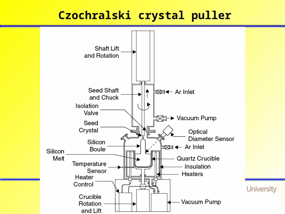
Czochralski technique:
• Small seed crystal dipped into molten Si bath and slowly withdrawn.
• The bath and growing “boule” are rotated in opposite directions.
• Argon atmosphere, impurities may be added for
doping.
School of Electrical and Electronic EngineeringQueen’s University Belfast, N.Ireland
Czochralski crystal puller
School of Electrical and Electronic EngineeringQueen’s University Belfast, N.Ireland
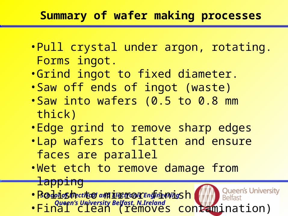
Summary of wafer making processes
• Pull crystal under argon, rotating. Forms ingot.• Grind ingot to fixed diameter.• Saw off ends of ingot (waste)• Saw into wafers (0.5 to 0.8 mm thick)• Edge grind to remove sharp edges• Lap wafers to flatten and ensure faces are
parallel• Wet etch to remove damage from lapping• Polish to mirror finish• Final clean (removes contamination)

School of Electrical and Electronic EngineeringQueen’s University Belfast, N.Ireland
• Silicon wafer manufacturing process

School of Electrical and Electronic EngineeringQueen’s University Belfast, N.Ireland
• The best sand comes from the beaches of Australia.
Pulling the crystal boule

School of Electrical and Electronic EngineeringQueen’s University Belfast, N.Ireland
• Diamond saw
• Polishing
• Ingots
Sawing and polishing

School of Electrical and Electronic EngineeringQueen’s University Belfast, N.Ireland

School of Electrical and Electronic EngineeringQueen’s University Belfast, N.Ireland
Standard wafer sizes

School of Electrical and Electronic EngineeringQueen’s University Belfast, N.Ireland
Removing impurities
• For high quality VLSI impurities can be reduced to a low level from device regions by gettering:
1. Impurities released into solid solution2. Impurities diffused through silicon3. Impurities trapped by dislocations or precipitates
• Extrinsic gettering creates damage or defects on backside of wafer. After annealing → dislocations
• Intrinsic gettering – precipitate supersaturated oxygen (out of wafer) into clusters → stress.
School of Electrical and Electronic EngineeringQueen’s University Belfast, N.Ireland
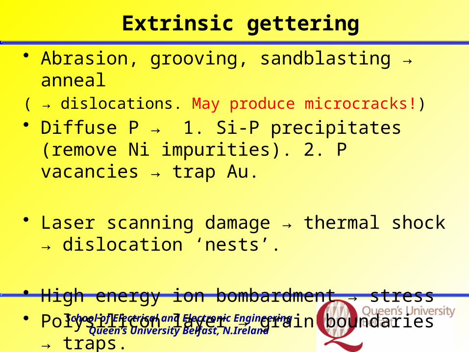
Extrinsic gettering
• Abrasion, grooving, sandblasting → anneal( → dislocations. May produce microcracks!)
• Diffuse P → 1. Si-P precipitates (remove Ni impurities). 2. P vacancies → trap Au.
• Laser scanning damage → thermal shock → dislocation ‘nests’.
• High energy ion bombardment → stress• Polysilicon layer → grain boundaries → traps.
School of Electrical and Electronic EngineeringQueen’s University Belfast, N.Ireland
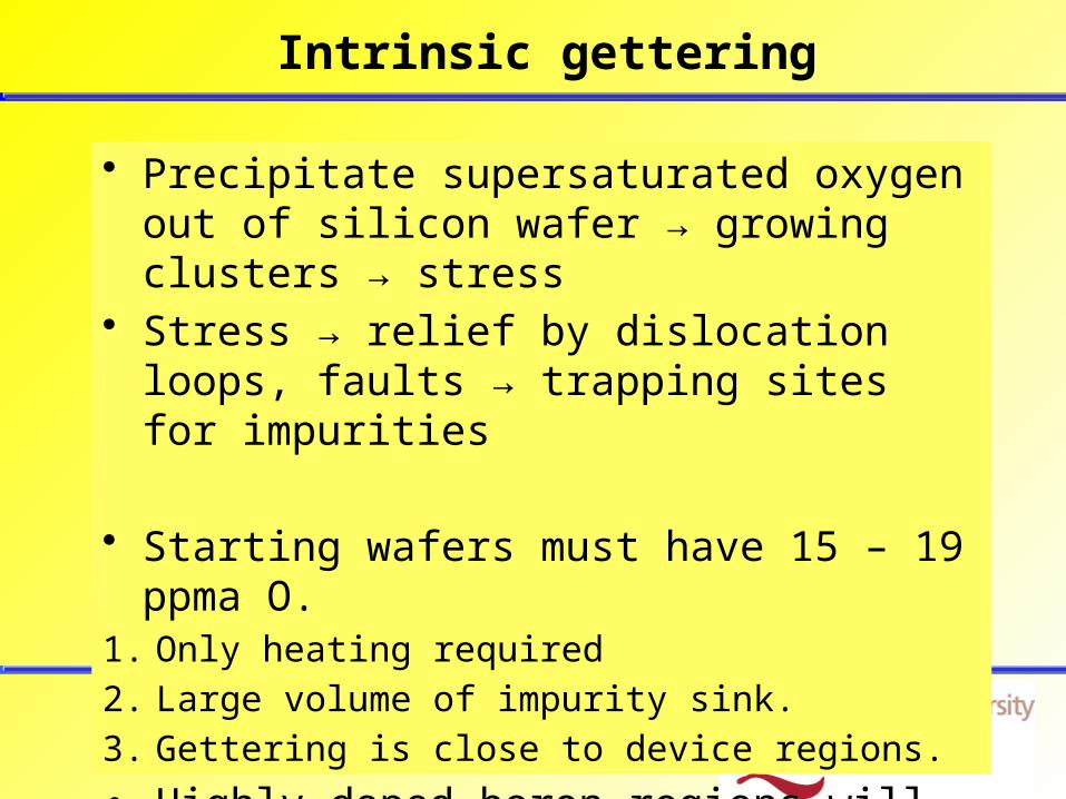
Intrinsic gettering
• Precipitate supersaturated oxygen out of silicon wafer → growing clusters → stress
• Stress → relief by dislocation loops, faults → trapping sites for impurities
• Starting wafers must have 15 – 19 ppma O.1. Only heating required
2. Large volume of impurity sink.
3. Gettering is close to device regions.
• Highly doped boron regions will getter Fe (B may be incorporated or high-doped B substrate + epitaxial layer)
School of Electrical and Electronic EngineeringQueen’s University Belfast, N.Ireland
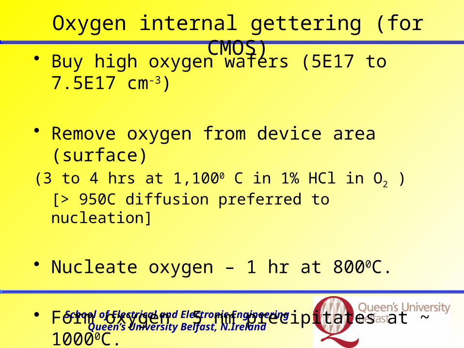
Oxygen internal gettering (for CMOS)
• Buy high oxygen wafers (5E17 to 7.5E17 cm-3)
• Remove oxygen from device area (surface)(3 to 4 hrs at 1,1000 C in 1% HCl in O2 ) [> 950C diffusion
preferred to nucleation]
• Nucleate oxygen – 1 hr at 8000C.
• Form oxygen 5 nm precipitates at ~ 10000C.(Precipitates create volume mismatch → dislocations)

School of Electrical and Electronic EngineeringQueen’s University Belfast, N.Ireland
• Oxygen-free zone > deepest active device area. Oxygen < 2E17 cm-3 .
(Oxygen can degrade device!)
• e.g. For CMOS with 250 nm feature size, oxygen-free zone >> 1.5 µm. (Use 2 hr steam cycle at 10000 C).
Oxygen internal gettering (for CMOS)

School of Electrical and Electronic EngineeringQueen’s University Belfast, N.Ireland
Oxygen internal gettering (for CMOS)

School of Electrical and Electronic EngineeringQueen’s University Belfast, N.Ireland
Oxygen nucleation rate and denuded (oxygen-free) zone depth

School of Electrical and Electronic EngineeringQueen’s University Belfast, N.Ireland
• Oxygen profile through the denuded zone
School of Electrical and Electronic EngineeringQueen’s University Belfast, N.Ireland
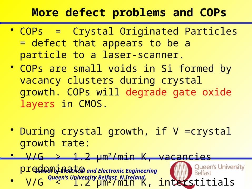
More defect problems and COPs
• COPs = Crystal Originated Particles = defect that appears to be a particle to a laser-scanner.
• COPs are small voids in Si formed by vacancy clusters during crystal growth. COPs will degrade gate oxide layers in CMOS.
• During crystal growth, if V =crystal growth rate:• V/G > 1.2 µm2/min K, vacancies predominate• V/G < 1.2 µm2/min K, interstitials predominate• G = axial temperature gradient near interface.

School of Electrical and Electronic EngineeringQueen’s University Belfast, N.Ireland
More defect problems and COPs
During crystal growth
if V =crystal growth rate:
V/G > 1.2 µm2/min K, vacancies predominate
V/G < 1.2 µm2/min K, interstitials predominate
G = axial temperature gradient near interface.
Hence slow cool silicon during crystal growth in temperature range ~ 11000 C. Also, high temperature annealing (see graph)

School of Electrical and Electronic EngineeringQueen’s University Belfast, N.Ireland
Number of LPDs v. depth of anneal (defects or particles)

School of Electrical and Electronic EngineeringQueen’s University Belfast, N.Ireland
Light point defects (LPDs), as in Figure.
• LPDs may be COPs or actual particles for 150 mm dia (100) Si after various anneals.
[Surface and depth(by polishing into crystal)]
• For 180 nm the COP goal was < 38COPs/200mm wafer or < 21COPs/150mm wafer.
• Thus, slow cooling and annealing to reduce COP levels become very critical as linewidths become smaller.