processor trends towards high performance 2.1 the...
TRANSCRIPT
26
2.1 The Conceptual Evolution of processors
The most motivating aspect of microprocessor evolution is keeping Moore’s law
alive. If we look at the journey from very first on chip microprocessor to the latest
one available in market it can be derived that series of new techniques have been
thought and in turn implemented to satisfy the greed for more speed and having
reduction in the size of the circuit initially. This greed is than transformed to the less
power consumption too in the processors which arrived later on after 1990. Some of
the techniques have been survived and some had been become obsolete. This chapter
presents the clear picture of this exciting journey of processor development with
comparative study of various actual processors as examples to throw light on the
road of processor technological development upto the multicore era from very
preliminary understanding of computer to the most advance technology. It helps in
justifying the need of such analytical and comparative study of the various
techniques of enhancing processor performance.
The Computer is a combination of hardware and software. Hardware means the parts
of a computer that we can see and touch and feel like the case and the circuit inside.
The most important example of hardware is a small chip inside our computer called
as microprocessor. It is major part of computer to which we can refer as brain of the
computer. It is the part that translates instructions and performs calculations.
Hardware items such as monitor, keyboard, mouse, printer, and other components
are often called hardware. The Software means the instructions, or programs, that
Chapter 2 Processor trends towards high performance

27
direct hardware about what to do. The Microsoft office - a kind of program that one
can use to write letters calculate audit reports, preparing presentation using the
computer is one type of software. The operating system is also software which helps
user in operating the computer and managing resources. Microprocessor is the main
and vital part of Computer. It is made up of many transistors fabricated on a single
chip. The size of microprocessor vary according to the length of the data and as per
the data format it may of of 4-bit , 8, 16,32 or 64-bit microprocessor. As the human
need is grown, as the technology has been grown the size of microprocessor in terms
of the data length (Maximum data bits processed at a time) is also grown.
2.1.1 The First Arrival of Microprocessor on Globe
The first fully functional processor from 4004 in 1971 to the Intel core i3 processor
journey is full of ups and downs but though it is literally succeeded in keeping
consistent growth both the speed as well as performance wise. In parallel to Intel the
other industries like Motorola, DEC (Digital Equipment Corporation) and TI (Texas
Instruments) had also launched the microprocessor in sequence of time. The various
vendors have designed microcomputers based on these processors and they were like
IBM, MIPS, Apple, and Sun etc.
Microcomputers arrived at the service of People :
Before 1980 the manual semiconductor chip design was existing. By invention of
VLSI design which was introduced in 1980 by Carver Mead and Lynn Convay. It
was a revolutionary point and later on they explained forming complex circuitry on a
single chip like pipeline and prefetch buffers etc. Analysis tools such as switch level
simulator and static timing analyzers have provided ease to designers for designing

28
the modules. The decade which started with 3 micron technology has reached upto
1.25 micron by the time 1985 arrived. The Intel 386DX was launched in 1985
having 1 micron gate length. The entire CPU was on a single die however FPU and
MMU still was on different chips. As time p assed CMOS became dominant on
NMOS due to its low power consumption. In mid-1980 GaAS was experimented
over silicon. The Desktop technology than started from hobby to business
applications and the first operating system supporting this was MS-DOS. Some basic
Desktop featured BASIC as the primary programming Language. Later on the wide
use of Unix and C-Programming accelerated the need of advance processors. Apple
introduced Apple-III in 1980 using 6502 having MODEM, Hard Disk and floppy
drive. In 1981 IBM launched a desktop using Intel 8088 having 64KB RAM and
40KB ROM and 4.77MHz clock with PC DOS 1.0 OS. In June 1982 IBM PC clone
was released. The availability of BIOS was the theme behind clone and once BIOS
is made available anyone can assemble PC was the concept. IBM continued to
develop with XT in 1983 having 10MB hard drive, 128KB RAM. IBM introduced
AT in 1984 with 6MHZ 80286 processor, 256KB RAM, 1.25MB floppy drive and
PC DOS 3.0 OS. The first Desktop based on 68000 was Apple Lisa in 1983 having
5MHz clock, 1MB RAM, 2MB ROM and 5MB hard drive. Lisa was the first
introducing GUI. Later on Apple introduce Macintosh based on 8MHz 68000 CPU.
The era began for IBM compatible and IBM clone PCs. The advances in application
were possible by having WordPerfect in 1982, Lotus1-2-3 in 1984 and first Desktop
publishing by Aldus Page Maker.

29
2.1.2 Before and after MS-DOS
The Operating System development was very interesting and it has very big impact
on the landscape of Microprocessor design. The Control Program/Monitor
abbreviated as CP/M was the first OS for Microprocessor based computer systems.
IBM contacted Digital Researchers for their CP/M-86 OS to be used for its future
microcomputers but they remain isolated and as a result after almost a decade cross
platform OS other than UNIX available to none X-86 systems. Microsoft at that time
was merely selling BASIC and FORTRAN Compilers. Seattle Computer products
(SCP) developed disk operating system due to delay in CP/M-86 for Intel 8086
based systems. Microsoft has got licence from SCP and the OS was than renamed as
MS-DOS in 1981. In 1985 than Microsoft introduced Windows 1.0 for X86 PCs.
2.1.3 Advance Microprocessors and RISC
The 16-Bit processor were developed which were having lower8-bit compatibility.
8086 was having two units like BIU and EU. It was a specific design having
Memory Segmentation and 20 bit physical address with six byte FIFO buffer for
storing instructions fetched in advance. Than later version 80286 came in market
having 16MB address space supporting separate FPU chip 80287.The 6800o had
linear address space with 32-bit address and data registers and simple pipeline. The
variant of Motorola 68000 like 68010 added virtual memory support and 68020 was
true 32-bit processor having true pipeline and overlapping operand fetch and
internal execution. Zilog variant Z8000 chosen to leave the compatibility with Z80
for taking better use of 16-bit registers and bus. The concept of RISC was already
evident in system like IBM 801 non microprocessor architecture. RISC used
Load/Store architecture and no memory to memory direct transfer with fixed length

30
instructions. In CISC there was a multi cycle execution but in contrast to that the
RISC processor employed single cycle execution. VAX IBM 370 was a CISC based
having small frequently used many instructions. The Research team at Berkeley and
Stanford have analysed and based on result designed RISC-I and RISC-II based on
large register file. RISC-I was having two stage pipeline and RISC-II with three
stage pipeline. This idea was than utilized in Sun’s SPARC architecture. The same
team started working on making compiler for performance enhancement and
considering system and compiler as a one system. They have started working on
Microprocessor without interlocking pipe stages(MIPS) for optimizing compiler
technology further.MIPS Architecture requires a kind of compiler capable of
managing all interlocking and data dependencies between instructions and control
dependencies of branches. They also introduced VLIW kind of structure where two
instructions incorporated in one 32-bit long instruction.
2.1.4 RISC on way proving superiority over CISC
Berkeley RISC and Stanford MIPS shown path for RISC based processor
development. The MIPS R2000 based on Stanford MIPS was launched in 1986. The
RISC processor was basically focused on performance and hence there was a big
competition between lower price CISC systems and higher performing UNIX based
RISC systems. The IBM Compatible PCs were lower in price as compared to Apple
Branded Macintosh. The upper advance processors as 80386 and 80486 were grown
in market due to the low cost and open standard.
Additional Architectural Features evolved in second Generation Advance processors
.The Pipeline is more deepened and designed having 5 stages. The Inclusion of Data
and Code cache Memory, on Chip floating point Unit along with Memory

31
management Unit are the additional features making the processors more powerful
and having improved performance over the past designs. All these were possible due
to advancement in Microelectronics and fabrication technology. The no. of
transistors increased from 275000 in 80386DX to 120000 in Intel 80486DX. The
Intel 80386 and Motorola 68020 are considered as the second generation CISC
processors with limited capacity pipeline. More than 30 new instructions were added
with MMU and 4 modes of privilege. Motortola launched 68030 in 1987 with 3
stage pipeline having 20MHz clock. Still the FPU was there as a separate chip to be
interfaced as coprocessor. The first CPU with on chip FPU and Cache Memory came
with 1 million transistors in one micron CMOS technology operating at clock speed
of 25MHz. In 1991 Motorola again came with 68040 with 1.2 million transistor, two
4K cache and on chip FPU.
2.1.5 RISC from various vendors
RISC processors basically inspired from Stanford MIPS and Berkeley RISC having
32-bit long instructions and single cycle execution. The Load and Store are the only
instructions to access Memory and Memory mapped I/O and hence it is also referred
as Load and Store architecture. Two separate source Registers from destination
register allowed reuse of registers unlike in CISC where one of the operand is
overwritten by the result. Big register file and two read and one write operation in
one cycle was the unique feature of RISC. The instruction decoding is made simple
and faster avoiding complex instructions. MIPS R2000 was the first commercial
available RISC microprocessor. Interlocks avoided and registers are ensured having
the latest value always and thus there is an insertion of one clock cycle delay by
compiler to ensure correct operation. The best feature that MIPS offered was loading

32
and storing misaligned data using only two instructions. Two special registers HI
and LO for holding quotient and remainder. The theme was to have processor with
efficient pipeline as there was no interlocks in MIPS. MIPS3000 was launched in
1989 having 144 pins and 54 sq-mm die clocked at 25 MHz. During which Intel
introduced 80486 having on chip FPU and 8K Cache on chip with 168 pins and 33
MHz clock with 165 sq-mm die size. But though Intel was cheaper than MIPS3000.
Parallel to that sun Microsystem had introduce SPARC named RISC based
architecture having unique feature of window register file which allows saving and
restoring registers while call of the program routine. It also had tagged addition
feature to support Artificial Intelligence languages.
2.1.6 RISC era & deeper pipeline Architecture
The middle generation microprocessor cam with deeper pipeline in RISC era. Intel,
AMD Motorola all have thought to introduce RISC and going on that line they gave
80960K, AMD 29000 and 88100 from Motorola for embedded feature support. But
the Motorola failed in competition with Intel and AMD. During this era RISC has
already been popular and looking to that New Advanced RISC Machine (ARM)
Architecture came in market. In general purpose computing the success of X86 was
extraordinary and hence other vendors like AMD also started building clones of
X86. The number of instructions per second and the clock frequency was the major
issue at that time. IBM, Motorola and Apple had joined hands to build RISC
processor and was named Power PC to cope up the threat of Intel but it this alliance
failed and during which Intel has just concentrated on market and launched designs
which is performance oriented keeping the theme aside whether it is RISC or CISC?
In the middle generation microprocessors it was necessary to highlight the

33
throughput and performance to project it among users and PC manufacturer. The
processor Designer have than used Standard Performance Evaluation Corporation
designed benchmarks later on called as SPEC Benchmarks. SPECint based on six
integer applications and SPECfp based on 14 different floating point operations.
Alpha 21064 and Power PC601 were the designs having Load and store structures
with 32-bit instructions and 32/64 bit register file. Alpha was a design with simple
instruction set, fast clocks and deep pipelines. On contrast Power PC had more
powerful instruction. Alpha has more number of instructions but at the cost of low
clocking and low CPI. The deeper and longer the pipeline, smaller and lower the
logical operation at particular stage and it directly resulted in faster clocking. Only
negative point of deeper pipeline is penalty we pay for branching and looping. This
can be avoided by introducing Branch prediction Unit. Looking to the simplicity and
64-bit architecture without 32-bit compatibility it was became wider choice over
Power PC. Only addressing mode in Alpha was Register plus whereas Power PC
provided register plus register as well with post modification of index register. Byte
alignment was done by separate instructions and hence the alpha load and store
pipeline was more simpler and allowing faster access to 8KB cache for instruction
and data. The Power PC601 had unified, eight ways set associative Cache which was
slow but offered high bit rate. Alpha has single instruction for testing conditions and
branching, whereas if same is to be done in alpha was requiring two instructions.
The alpha had 7-stage integer pipe and 10-stage floating point pipe on contrast
Power PC601 had shorter pipelines. As the deep pipeline increases branch
latency(number of idle cycles caused by branching).To compensate this Alpha
designer have included dynamic branch prediction unit maintaining the history table
34
of most recent as well as frequent branching. The Power PC was poor in this area
having simple static branch prediction.
2.1.7 Super pipeline architecture and Intel dominancy
In year 1992 MIPS 4000 was launched having super pipelined 64-bit architecture.
Address and data bus doubled with high clock frequency of 100MHz. It was mainly
used in Graphics and game machines. Sun also came with super Sparc having dual
processor but remained non popular. The SUN came back into the picture by launch
of UltraSparc having 167MHZ clock, two integer Units, 5 Floating point Units , A
branch Unit and A load/Store unit . The Cache were 16K having direct mapped
cache for data and 2-way set associative for address. Visual Instruction set for pixel
processing was the unique feature introduced first time. It has supported Motion
Picture Expert Group (MPEG) standards in estimating the speed of motions
computations. In this race HP also joined and designed PA-RISC 7100 and 7200 32-
bit processor series having high speed external cache to be used using static RAMs.
The PA-RISC 8000 180MHz was first 64-bit processor from HP launched in 1996.
All new processor generally were dominating older one only the Alpha which
became poular for a decade or long over its newly arrived processors.
The Intel dominancy :
After invention of Mouse Microsoft designed interactive OS called Windows 3.o for
IBM pC. The large market was covered by the windows based IBM PC. 80386 and
80486 were cloned by manufacturer called AMD and CYRIX. To be distinguished
from all these clones and other trademark problem Intel had changed name of its
80586 processor as Pentium. Pentium was launched having Super scaled pipeline, 60

35
MHz clock , two integer pipes, dual instruction issue, deep pipelines, separate data
and code Cache and made up of BiCMOS technology to get more speed than
CMOS. The clock was than increased to 100MHz without major changes. The
Macintosh system based on Power PC at that time was costlier and that is why apple
slowly loose the market. In year 1995 Microsoft launched Windows- 95 OS having
device recognition and with facility for installation of CD-ROM drive , printers ,
modems etc. Windows NT was prior introduction to the workstation having database
management and spread sheets applications with multi-tasking. The Pentium was
further improved and launched as Pentium pro in 1996.Many new pixel recessing
instructions were added for animation and graphics processing improvement which
was a feature declared as MMX. Having more facilities and inspite of that cut in
price put Intel in the leading processor manufacturer and seller of that time. Still
AMD and CYRIX of followed but was a bit lagging to Intel all the time.
2.1.8 Speed increasing mechanism and thermal Problem
The method which was employed in year 1995 and ahead to increase speed was by
increasing the clock frequency and making devices faster by using improved
fabrication technologies. Reducing delay in flow of data between gates and faster
switching of transistors. But the great loop hall found of this approach was more
power consumption and in turn heat generation. The solution found at that time was
to drop the voltage to 2 to 3 volts which had reduced the power consumption by
considerable amount. The solution of heat was solved by proper heat sink and fan
cooling methods. Out of order issue, Speculative Execution, Branch prediction,
Register Renaming and prefetch buffers all have increased complexity. It was
challenge to have such kind of processor having no bugs. Floating point division was

36
a kind of bug which Intel was not at all happy with and Intel was in big trouble for
some time due to this bug.
The shrinking line width of the IC of the next generation IC was in need of better
and more sophisticated lithographic techniques to draw more and finer lines. It was
made possible at that time to reduce an intrinsic delay and hence increasing clock by
same proportion. Later on Resistance – Capacitance delay became prominent at high
clock. Attempt was made to lower resistance by using aluminium instead of copper
and using lower dielectric constant insulator for reducing capacitance. Now delay
remained significance is only due to interconnects. Again after saturation designer
have looked towards VLIW approach making processor more complex and
exploring the rigorous parallelism. Multiple operations in one very long instruction
word brought extensive parallelism into action. The problem of requirement of fast
buses for feeding multiple processors was the challenge.
2.1.9 Chip Multi Processing (CMP) and Multicore Era
The traditional way of increasing speed of processor was to increase the clock
frequency and by higher package densities including more hardware to cope up with
the more work in less time. The increased power dissipation due to increasing clock
put the physical limitation and hence it became difficult to get speed enhancement
simply by this traditional approach. CMP came to existence when it was decided to
add more transistors and fabricating more number of processor threads on same chip
to carry out parallel processing and exchange of hardware, later on this architecture
was known as Multi Core processor Technology. According to flynn’s classification
it is real MOMD architecture. On the lowest level, the execution unit itself can have
a super-scalar architecture. A hardware-controlled parallel usage of execution unit
37
components enables the execution of multiple processor instructions during one
clock cycle. This approach of instruction-level parallelism (ILP) is limited, but
widely realized approach in modern processor designs. Each execution unit can
additionally support the concept of a logical processor, which allows a simultaneous
multi-threading (SMT) inside the processor pipeline. This approach allows to hide
data access latencies for some of the threads, by utilizing the execution unit for other
tasks during a blocking period. This realizes a virtual sharing of one execution unit
within a processor. SMT is better known under the marketing term hyper threading
from Intel. It maintains the architectural state of the execution unit (mostly CPU
registers) separately per logical processor, in order to allow context switching in
hardware. Each processor has its own L1 Cache and separate L2 Cache. The speed
can be increased by having more and more number of execution units. It may range
from few ten to one thousand even in forthcoming years. It is possible to keep
Moore’s law alive by this technology. There are two concepts developed like
homogeneous cores having similar simple many cores and other approach of having
heterogeneous architecture having one master processor and others like vector
processor or small slave processors. This type of task level parallelism is popular in
dedicated systems like for graphics and other scientific applications. The Intel
launched Core-i5 , i-7 and i-3 processors in 2008 , 2009 and 2010 respectively. The
major change took place in last few years where the design philosophy had been
changed from Single core processor to Multi core processor design. The ILP
(Instruction level Parallelism had been seen as the only way to get increased
performance .How to make the best use of cores is now central theme. It always
depend on application whether parallel architecture is helping in getting improved
performance or not? The task involving much similar parallel operations may be

38
more benefited by similar parallel cores but in each case it will not be the experience
at all. Many applications are lagging in providing inherent TLP making
parallelization impossible. In such cases the advantage of Multicore processor will
only be possible if heterogeneous cores are used according to requirement. The
parallel applications divided into several similar operations and can be operated
using homogeneous cores.
2.2 Emerging Processor Technology Trends
The revolution of computer system has moved up enormously. From the age of
heavy, bulky and large sized computers today we have moved to thinnest notebooks.
From the era of simple 4 bit Intel 4004 processors, we have moved up to Intel Core
i7 extremes. From the first computer named as ENIAC, we now have palmtops.
There had been a lot of changes in the way of computing technology. The design
direction is moved towards multi core processors from the single core processors.
Single core processors who served the computing generation for quite a long time is
now vanishing. It’s the Multi-core CPUs that are in action now. With lots of new
functionality, great features, new up gradation Multicore processors are surely the
future product. The purpose of this study is to carry out comparative studies of all
design concepts with pro and cones and highlighting the techniques, idea as well as
design concept which is more useful in designing the modern High performance
computer satisfying the Moore’s law.
The processor technology is observed changing at such a fast rate that it is almost
difficult for the supporting technology designers to meet the need of the customers.
The Number of transistor per chip: The Fig.2.1 shows the trend of increase in
number of transistors from basic 4004 to the predicted future microprocessors.
Core i7 4770K is 177 millimeters squared and it features 1.4 billion transistors on

39
chip. The size reduction is also going on in parallel which in turn increasing the
device density. It had lead to many problems which had been tackled and still we
are struggling.
Fig 2.1 Processor evolution in light of Moore’s law
The reduction manufacturing process size: The Fig.2.1 shows the trend how
manufacturing process size reduction is achieved from 182 nm to 22 nm and the
research is going on for getting 14nm soon till the end of year 2014.

40
Fig.2.2 Manufacturing process size evolution in light of Moore’s law
Fig.2.3 Combined projection of evolution in number of transistor & process
technology
2.2.1 Obsolete Single Core Processor
A processor containing a single core is known as single core processor. If we see in
depth the single core processor architecture consists of several parts like he

41
processor core, two levels of cache, a memory controller , three coherent
HyperTransport (CHT) links, and a non-blocking crossbar switch that connects the
parts together. A single-core Opteron processor design is illustrated in Fig.2.4. The
CHT links may be connected to another processor or to peripheral devices. The
NUMA design is apparent from the diagram, as each processor in a system has its
own local memory, memory to which it is closer than any other processor. Memory
commands may come from the local core or from another processor or a device over
a CHT link. In the latter case the command comes from the CHT link to the crossbar
and from there to the MCT.
Fig 2.4 Single core processor Block Diagram
The local processor core does not see or have to process outside memory commands,
although some commands may cause data in cache to be invalidated or flushed from
cache.
2.2.2 Speed enhancement efforts
As touched upon above, from the introduction of Intel’s 8086 through the Pentium 4
an increase in performance, from one generation to the next, was seen as an increase

42
in processor frequency. For example, the Pentium 4 ranged in speed (frequency)
from 1.3 to 3.8 GHz over its 8 year lifetime. The physical size of chips decreased
while the number of transistors per chip increased; clock speeds in-creased which
boosted the heat dissipation across the chip to a dangerous level. To gain
performance within a single core many techniques are used. Superscalar processors
with the ability to issue multiple instructions concurrently are the standard. In these
pipelines, instructions are pre-fetched, split into sub components and executed out of
order. A major focus of computer architects is the branch instruction. Branch
instructions are the equivalent of a fork in the road; the processor has to gather all
necessary information before making a decision. In order to speed up this process,
the processor predicts which path will be taken, if the wrong path is chosen the
processor must throw out any data computed while taking the wrong path and
backtrack to take the correct path. Often even when an incorrect branch is taken the
effect is equivalent to having waited to take the correct path. Branches are also
removed using loop unrolling and sophisticated neural network-based predict-tors
are used to minimize the miss prediction rate. Other techniques used for performance
enhancement include register renaming, trace caches, reorder buffers,
dynamic/software scheduling, and data value prediction. There have also been
advances in power- and temperature-aware architectures. There are two flavors of
power-sensitive architectures: low-power and power aware designs. Low power
architectures minimize power consumption while satisfying performance constraints,
e.g. embedded systems where low-power and real-time performance are vital.
Power-aware architectures maximize performance parameters while satisfying power
constraints. Temperature aware design uses simulation to determine where hot spots
43
lie on the chips and revises the architecture to decrease the number and effect of hot
spots.
2.2.3 Why switching Multicore technology?
It is well-recognized that computer processors have increased in speed and decreased
in cost at a tremendous rate for a very long time. This observation was first made
popular by Gordon Moore in 1965, and is commonly referred to as Moore’s Law.
Specifically, Moore’s Law states that the advancement of electronic manufacturing
technology makes it possible to double the number of transistors per unit area about
every 12 to 18 months. It is this advancement that has fueled the phenomenal growth
in computer speed and accessibility over more than four decades. Smaller transistors
have made it possible to increase the number of transistors that can be applied to
processor functions and reduce the distance signals must travel, allowing processor
clock frequencies to soar. This simultaneously increases system performance and
reduces system cost. All of this is well-understood. But lately Moore’s Law has
begun to show signs of failing. It is not actually Moore’s Law that is showing
weakness, but the performance increases people expect and which occur as a side
effect of Moore’s Law. One often associates performance with high processor clock
frequencies. In the past, reducing the size of transistors has meant reducing the
distances between the transistors and decreasing transistor switching times.
Together, these two effects have contributed significantly to faster processor clock
frequencies. Another reason processor clocks could increase is the number of 2
transistors available to implement processor functions. Most processor functions, for
example, integer addition, can be implemented in multiple ways. One method uses
very few transistors, but the path from start to finish is very long. Another method
shortens the longest path, but it uses many more transistors. Clock frequencies are

44
limited by the time it takes a clock signal to cross the longest path within any stage.
Longer paths require slower clocks. Having more transistors to work with allows
more sophisticated implementations that can be clocked more rapidly. But there is a
down side. As processor frequencies climb, the amount of waste heat produced by
the processor climbs with it. The ability to cool the processor inexpensively within
the last few years has become a major factor limiting how fast a processor can go.
This is offset, somewhat, by reducing the transistor size because smaller transistors
can operate on lower voltages, which allows the chip to produce less heat.
Unfortunately, transistors are now so small that the quantum behavior of electrons
can affect their operation. According to quantum mechanics, very small particles
such as electrons are able to spontaneously tunnel, at random, over short distances.
The transistor base and emitter are now close enough together that a measurable
number of electrons can tunnel from one to the other, causing a small amount of
leakage current to pass between them, which causes a small short in the transistor.
As transistors decrease in size, the leakage current increases. If the operating
voltages are too low, the difference between a logic one and a logic zero becomes
too close to the voltage due to quantum tunneling, and the processor will not operate.
In the end, this complicated set of problems allows the number of transistors per unit
area to increase, but the operating frequency must go down in order to be able to
keep the processor cool. This issue of cooling the processor places processor
designers in a dilemma. The approach toward making higher performance has
changed. The market has high expectations that each new generation of processor
will be faster than the previous generation, if not why one should buy it? But
quantum mechanics and thermal constraints may actually make successive
generations slower. On the other hand, later generations will also have more

45
transistors to work with and they will require less power. Speeding up processor
frequency had run its course in the earlier part of this decade, computer architects
needed a new approach to improve performance. Adding an additional processing
core to the same chip would, in theory, result in twice the performance and dissipate
less heat; though in practice the actual speed of each core is slower than the fastest
single core processor. In September 2005 the IEE Review noted that “power
consumption increases by 60% with every 400MHz rise in clock speed”. So, what is
a designer to do? Manufacturing technology has now reached the point where there
are enough transistors to place two processor cores a dual core processor on a
single chip. The tradeoff that must now be made is that each processor core is slower
than a single-core processor, but there are two cores, and together they may be able
to provide greater throughput even though the individual cores are slower. Each
following generation will likely increase the number of cores and decrease the clock
frequency. The slower clock speed has significant implications for processor
performance, especially in the case of the AMD Opteron processor. The fastest dual-
core Opteron processor will have higher throughput than the fastest single core
Opteron, at least for workloads that are processor core limited, but each task may be
completed more slowly. The application does not spend much time waiting for data
to come from memory or from disk, but finds most of its data in registers or cache.
Since each core has its own cache, adding the second core doubles the available
cache, making it easier for the working set to fit. For dual core to be effective, the
work load must also have parallelism that can use both cores. When an application is
not multi threaded, or it is limited by memory performance or by external devices
such as disk drives, dual core may not offer much benefit, or it may even deliver less
performance. Opteron processors use a memory controller that is integrated into the

46
same chip and is clocked at the same frequency as the processor. Since dual core
processors use a slower clock, memory latency will be slower for dual core Opteron
processors than for single core, because commands take longer to pass through the
memory controller. Applications that perform a lot of random access read and write
operations to memory, applications that are latency bound, may see lower
performance using dual core. On the other hand, memory bandwidth increases in
some cases. Two cores can provide more sequential requests to the memory
controller than can a single core, which allows the controller to intern eave
commands to memory more efficiently. Another factor that affects system
performance is the operating system. The memory architecture is more complex, and
an operating system not only has to be aware that the system is NUMA (that is, it has
Non- Uniform Memory Access), but it must also be prepared to deal with the more
complex memory arrangement. It must be dual-core-aware. The performance
implications of operating systems that are dual core aware will not be explored here,
but we state without further justification that operating systems without such
awareness show considerable variability when used with dual core processors.
Operating systems that are dual-core-aware show better performance, though there is
still room for improvement.
2.2.4 The study of Multicore Fundamentals
The following isn’t specific to any one multicore design, but rather is a basic
overview of multi-core architecture. Although manufacturer designs differ from one
another, multicore architectures need to look at certain aspects. The basic
configuration of a microprocessor is seen in Fig.2.5 with multicore concept and
Fig.2.6 with a distributed memory model.
47
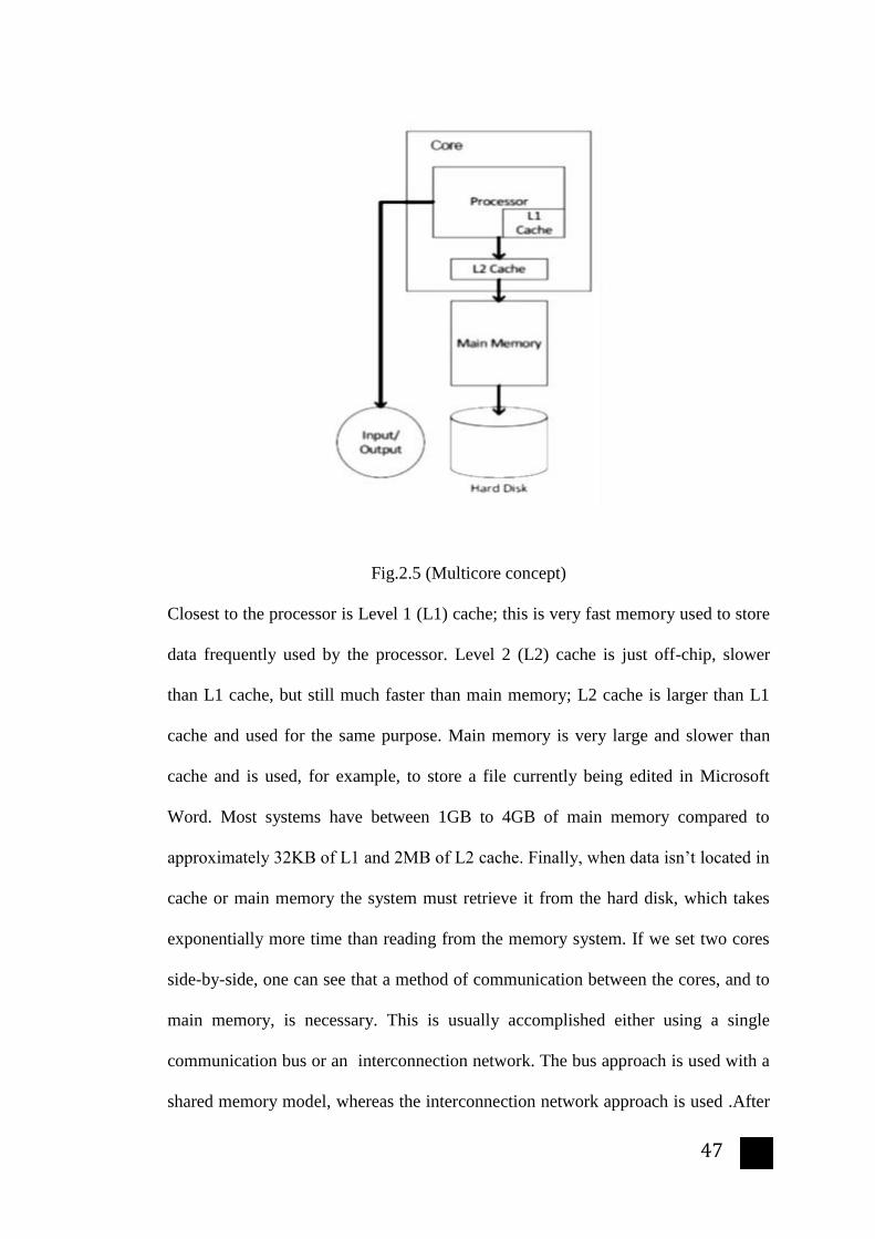
Fig.2.5 (Multicore concept)
Closest to the processor is Level 1 (L1) cache; this is very fast memory used to store
data frequently used by the processor. Level 2 (L2) cache is just off-chip, slower
than L1 cache, but still much faster than main memory; L2 cache is larger than L1
cache and used for the same purpose. Main memory is very large and slower than
cache and is used, for example, to store a file currently being edited in Microsoft
Word. Most systems have between 1GB to 4GB of main memory compared to
approximately 32KB of L1 and 2MB of L2 cache. Finally, when data isn’t located in
cache or main memory the system must retrieve it from the hard disk, which takes
exponentially more time than reading from the memory system. If we set two cores
side-by-side, one can see that a method of communication between the cores, and to
main memory, is necessary. This is usually accomplished either using a single
communication bus or an interconnection network. The bus approach is used with a
shared memory model, whereas the interconnection network approach is used .After

48
approximately 32 cores the bus is overloaded with the amount of processing,
communication, and competition, which leads to diminished performance therefore a
communication bus has a limited scalability.
Fig.2.6 (Multicore processor designs)
Thus in order to continue delivering regular performance improvements for general-
purpose processors, manufacturers such as Intel and AMD have turned to multi-core
designs, sacrificing lower manufacturing-costs for higher performance in some
applications and systems. Multi-core architectures are being developed, but so are
the alternatives. An especially strong contender for established markets is the further
integration of peripheral functions into the chip. The above two figures shows the
actual implementation of multi-core processor with shared memory and distributed
memory. As with any technology, multicore architectures from different
manufacturers vary greatly. Along with differences in communication and memory
configuration another variance comes in the form of how many cores the
microprocessor has. And in some multicore architecture different cores have
different functions, hence they are heterogeneous. Differences in architectures are
Cache
Processor
Cache
Single Bus
Memory
Processor
or
Processor
or Cache
I/O
Processor
or
Cache
Processor
or
Cache
Processor
or
Cache
Memory
or
Memory
or
Memory
or
Network

49
discussed below for Intel’s Core 2 Duo, Advanced Micro Devices‟ Athlon 64 X2,
Sony-Toshiba- IBM‟s CELL Processor, and finally Tilera’s TILE64.
2.3 Comparative study of various processor in Multicore domain
2.3.1 Intel & AMD Dual-Core Processor
Intel and AMD are the mainstream manufacturers of microprocessors. Intel produces
many different flavors of multicore processors: the Pentium D is used in desktops,
Core 2 Duo is used in both laptop and desktop environments, and the Xeon
processor is used in servers. AMD has the Althon lineup for desktops, Turion for
laptops, and Opteron for servers/workstations. Although the Core 2 Duo and Athlon
64 X2 run on the same platforms their architectures differ greatly.
Fig 2.7 (a) Intel Core 2 Duo (b) AMD Athlon 64 X2
Figure 6 shows block diagrams for the Core 2 Duo and Athlon 64 X2, respectively.
Both the Intel and AMD popular in the market of Microprocessors. Both
architectures are homogenous dual-core processors. The Core 2 Duo adheres to a
shared memory model with private L1 caches and a shared L2 cache which
“provides a peak transfer rate of 96 GB/sec.” If a L1 cache miss occurs both the L2
cache and the second core’s L1 cache are traversed in parallel before sending a
50
request to main memory. In contrast, the Athlon follows a distributed memory model
with discrete L2 caches. These L2 caches share a system request interface,
eliminating the need for a bus. The system request interface also connects the cores
with an on-chip memory controller and an interconnect called Hyper Transport.
Hyper Transport effectively reduces the number of buses required in a system,
reducing bottlenecks and increasing bandwidth. The Core 2 Duo instead uses a bus
interface. The Core 2 Duo also has explicit thermal and power control unit’s on-chip.
There is no definitive performance advantage of a bus v/s an interconnect, and the
Core 2 Duo and Athlon 64 X2 achieve similar performance measures, each using a
different communication protocol.
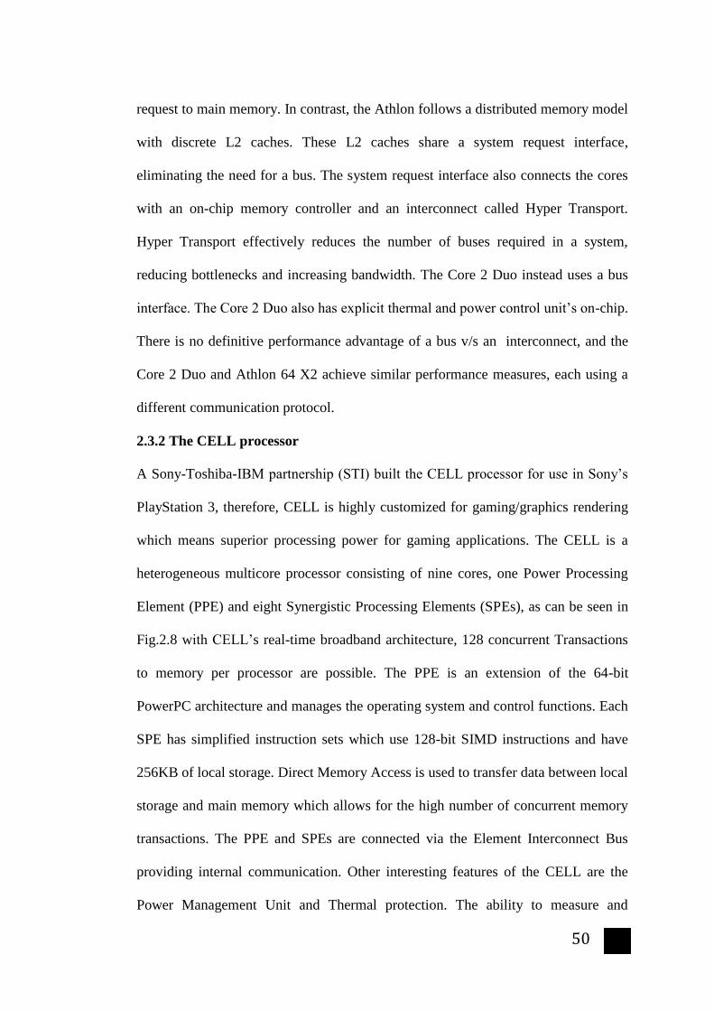
2.3.2 The CELL processor
A Sony-Toshiba-IBM partnership (STI) built the CELL processor for use in Sony’s
PlayStation 3, therefore, CELL is highly customized for gaming/graphics rendering
which means superior processing power for gaming applications. The CELL is a
heterogeneous multicore processor consisting of nine cores, one Power Processing
Element (PPE) and eight Synergistic Processing Elements (SPEs), as can be seen in
Fig.2.8 with CELL’s real-time broadband architecture, 128 concurrent Transactions
to memory per processor are possible. The PPE is an extension of the 64-bit
PowerPC architecture and manages the operating system and control functions. Each
SPE has simplified instruction sets which use 128-bit SIMD instructions and have
256KB of local storage. Direct Memory Access is used to transfer data between local
storage and main memory which allows for the high number of concurrent memory
transactions. The PPE and SPEs are connected via the Element Interconnect Bus
providing internal communication. Other interesting features of the CELL are the
Power Management Unit and Thermal protection. The ability to measure and

51
account for power and temperature changes has a great advantage in that the
processor should never overheat or draw too much power.
Fig.2.8 ( Cell Processor Internal Diagram )
2.3.3 Tilera TILE64
Tilera has developed a multicore chip with 64 homogeneous cores set up in a grid,
shown in Fig.2.9. An application that is written to take advantage of these additional
cores will run far faster than if it were run on a single core. Imagine having a project
to finish, but instead of having to work on it alone you have 64 people to work for
you. Each processor has its own L1 and L2 cache for a total of 5MB on-chip and a
switch that connects the core into the mesh network rather than a bus or interconnect.
The TILE64 also includes on-chip memory and I/O controllers. Like the CELL
processor, unused tiles (cores) can be put into a sleep mode to further decrease
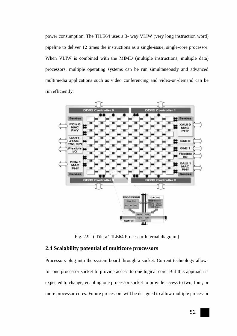
52
power consumption. The TILE64 uses a 3- way VLIW (very long instruction word)
pipeline to deliver 12 times the instructions as a single-issue, single-core processor.
When VLIW is combined with the MIMD (multiple instructions, multiple data)
processors, multiple operating systems can be run simultaneously and advanced
multimedia applications such as video conferencing and video-on-demand can be
run efficiently.
Fig. 2.9 ( Tilera TILE64 Processor Internal diagram )
2.4 Scalability potential of multicore processors
Processors plug into the system board through a socket. Current technology allows
for one processor socket to provide access to one logical core. But this approach is
expected to change, enabling one processor socket to provide access to two, four, or
more processor cores. Future processors will be designed to allow multiple processor
53
cores to be contained inside a single processor module. For example, a tightly
coupled set of dual processor cores could be designed to compute independently of
each other allowing applications to interact with the processor cores as two separate
processors even though they share a single socket. This design would allow the OS
to thread the application across the multiple processor cores and could help improve
processing efficiency. A multicore structure would also include cache modules.
These modules could either be shared or independent. Actual implementations of
multicore processors would vary depending on manufacturer and product
development over time. Variations may include shared or independent cache
modules, bus implementations, and additional threading capabilities such as Intel
Hyper- Threading (HT) Technology. A multicore arrangement that provides two or
more low clock speed cores could be designed to provide excellent performance
while minimizing power consumption and delivering lower heat output than
configurations that rely on a single high clock speed core. The following example
shows how multicore technology could manifest in a standard server configuration
and how multiple low clock speed cores could deliver greater performance than a
single high clock speed core for networked applications. This example uses some
simple math and basic assumptions about the scaling of multiple processors and is
included for demonstration purposes only. Until multicore processors are available,
scaling and performance can only be estimated based on technical models. The
example described in this article shows one possible method of addressing relative
performance levels as the industry begins to move from platforms based on single-
core processors to platforms based on multicore processors. Other methods are
possible, and actual processor performance and processor scalability are tied to a
variety of platform variables, including the specific configuration and application

54
environment. Several factors can potentially affect the internal scalability of multiple
cores, such as the system compiler as well as architectural considerations including
memory, I/O, front side bus (FSB), chip set, and so on. For instance, enterprises can
buy a dual-processor server today to run Microsoft Exchange and provide e-mail,
calendaring, and messaging functions. Dual-processor servers are designed to deliver
excellent price/performance for messaging applications
Fig. 2.10 ( Dual 3.6 GHz Xeon processors )
A typical configuration might use dual 3.6 GHz 64-bit Intel Xeon™ processors
supporting HT Technology. In the future, organizations might deploy the same
application on a similar server that instead uses a pair of dual-core processors at a
clock speed lower than 3.6 GHz. The four cores in this example configuration might
each run at 2.8 GHz. The following simple example can help explain the relative
performance of a low clock speed, dual-core processor versus a high clock speed,
dual-processor counterpart. Dual-processor systems available today offer a
scalability of roughly 80 percent for the second processor, depending on the OS,
application, compiler, and other factors. That means the first processor may deliver
100 percent of its processing power, but the second processor typically suffers some
55
overhead from multiprocessing activities. As a result, the two processors do not scale
linearly that is, a dual processor system does not achieve a 200 percent performance
increase over a single-processor system, but instead provides approximately 180
percent of the performance that a single-processor system provides. In this article,
the single-core scalability factor is referred to as external, or socket-to-socket,
scalability. When comparing two single-core processors in two individual sockets,
the dual 3.6 GHz processors would result in an effective performance level of
approximately 6.48 GHz. For multicore processors, administrators must take into
account not only socket-to-socket scalability but also internal, or core to core,
scalability, the scalability between multiple cores that reside within the same
processor module. In this example, core to core scalability is estimated at 70 percent,
meaning that the second core delivers 70 percent of its processing power. Thus, in
the example system using 2.8 GHz dual-core processors, each dual core processor
would behave more like a 4.76 GHz processor when the performance of the two
cores 2.8 GHz plus 1.96 GHz is combined. For demonstration purposes, this
example assumes that, in a server that combines two such dual-core processors
within the same system architecture, the socket to socket scalability of the two dual
core processors would be similar to that in a server containing two single core
processors—80 percent scalability. This would lead to an effective performance
level of 8.57 GHz. To continue the example comparison by postulating that socket
to socket scalability would be the same for these two architectures, a multicore
architecture could enable greater performance than single-core processor
architecture, even if the processor cores in the multicore architecture are running at a
lower clock speed than the processor cores in the single core architecture. In this
way, a multicore architecture has the potential to deliver higher performance than
56
single-core architecture for enterprise applications. On-going progress in processor
designs has enabled servers to continue delivering increased performance, which in
turn helps fuel the powerful applications that support rapid business growth.
However, increased performance incurs a corresponding increase in processor power
consumption and heat is a consequence of power use. As a result, administrators
must determine not only how to supply large amounts of power to systems, but also
how to contend with the large amounts of heat that these systems generate in the data
Centre.
2.5 Multicore Design Challenges
Having multiple cores on a single chip gives rise to some problems and challenges.
Power and temperature management are two concerns that can increase
exponentially with the addition of multiple cores. Memory/cache coherence is
another challenge, since all designs discussed above have distributed L1 and in some
cases L2 caches which must be coordinated. And finally, using a multicore processor
to its full potential is another issue. If programmers don’t write applications that take
advantage of multiple cores there is no gain, and in some cases there is a loss of
performance. Application need to be written so that different parts can be run
concurrently.
2.5.1 Power and Temperature
If two cores were placed on a single chip without any modification, the chip would,
in theory, consume twice as much power and generate a large amount of heat. In the
extreme case, if a processor overheats your computer may even combust. To account
for this each design above runs the multiple cores at a lower frequency to reduce
power consumption. To combat unnecessary power consumption many designs also
incorporate a power control unit that has the authority to shut down unused cores or

57
limit the amount of power. By powering off unused cores and using clock gating the
amount of leakage in the chip is reduced. To lessen the heat generated by multiple
cores on a single chip, the chip is architected so that the number of hot spots doesn’t
grow too large and the heat is spread out across the chip. The majority of the heat in
the CELL processor is dissipated in the Power Processing Element and the rest is
spread across the Synergistic Processing Elements. The CELL processor follows a
common trend to build temperature monitoring into the system, with its one linear
sensor and ten internal digital sensors.
2.5.2 Cache Coherence
Coherence is a concern in a multicore environment because of distributed L1 and L2
cache. Since each core has its own cache, the copy of the data in that cache may not
always be the most up-to-date version. For example, imagine a dual-core processor
where each core brought a block of memory into its private cache. One core writes a
value to a specific location; when the second core attempts to read that value from its
cache it won’t have the updated copy unless its cache entry is invalidated and a
cache miss occurs. This cache miss forces the second core’s cache entry to be
updated. If this coherence policy wasn’t in place garbage data would be read and
invalid results would be produced, possibly crashing the program or the entire
computer. In general there are two schemes for cache coherence, a snooping protocol
and a directory-based protocol. The snooping protocol only works with a bus based
system, and uses a number of states to determine whether or not it needs to update
cache entries and if it has control over writing to the block. The directory-based
protocol can be used on an arbitrary network and is, there-fore, scalable to many
processors or cores, in contrast to snooping which isn’t scalable. In this scheme a
directory is used that holds information about which memory locations are being

58
shared in multiple caches and which are used exclusively by one core’s cache. The
directory knows when a block needs to be updated or invalidated. Intel’s Core 2 Duo
tries to speed up cache coherence by being able to query the second core’s L1 cache
and the shared L2 cache simultaneously. Having a shared L2 cache also has an added
benefit since a coherence protocol doesn’t need to be set for this level. AMD‟s
Athlon 64 X2, however, has to monitor cache coherence in both L1 and L2 caches.
This is sped up using the Hyper Transport connection, but still has more overhead
than Intel’s model.
2.5.3 Multithreading
The last, and most important, issue is using multithreading or other parallel
processing techniques to get the most performance out of the multicore processor.
Also to get the full functionality we have to have program that support the feature of
TLP. Rebuilding applications to be multithreaded means a complete rework by
programmers in most cases. Programmers have to write applications with
subroutines able to be run in different cores, meaning that data dependencies will
have to be resolved or accounted for (e.g. latency in communication or using a
shared cache). Applications should be balanced. If one core is being used much more
than another, the programmer is not taking full advantage of the multi-core system.
Some companies have heard the call and designed new products with multicore
capabilities; Microsoft and Apple’s newest operating systems can run on up to 4
cores, for example.
2.5.4 Crucial design Issues
With numerous cores on a single chip there is an enormous need for increased
memory. 32-bit processors, such as the Pentium 4, can address up to 4GB of main
memory. With cores now using 64-bit addresses the amount of addressable memory
59
is almost infinite. An improved memory system is a necessity; more main memory
and larger caches are needed for multithreaded multiprocessors.
System Bus and Interconnection Networks
Extra memory will be useless if the amount of time required for memory requests
doesn’t improve as well. Redesigning the interconnection network between cores is a
major focus of chip manufacturers. A faster network means a lower latency in inter-
core communication and memory transactions. Intel is developing their Quick path
interconnect, which is a 20- bit wide bus running between 4.8 and 6.4 GHz; AMD‟s
new HyperTransport 3.0 is a 32-bit wide bus and runs at 5.2 GHz. A different kind
of interconnect is seen in the TILE64‟s iMesh, which consists of five networks used
to fulfill I/O and off-chip memory communication. Using five mesh networks gives
the Tile architecture a per tile (or core) bandwidth of up to 1.28 Tbps (terabits per
second).
Parallel Programming:
In May 2007, Intel fellow Shekhar Borkar stated that “The software has to also start
following Moore’s Law, software has to double the amount of parallelism that it can
support every two years.” Since the number of cores in a processor is set to double
every 18 months, it only makes sense that the software running on these cores takes
this into account. Ultimately, programmers need to learn how to write parallel
programs that can be split up and run concurrently on multiple cores instead of
trying to exploit single-core hardware to increase parallelism of sequential programs.
Developing software for multicore processors brings up some latent concerns. How
does a programmer ensure that a high priority task gets priority across the processor,
not just a core? In theory even if a thread had the highest priority within the core on
which it is running it might not have a high priority in the system as a whole.
60
Another necessary tool for developers is debugging. However, how do we guarantee
that the entire system stops and not just the core on which an application is running?
These issues need to be addressed along with teaching good parallel programming
practices for developers. Once programmers have a basic grasp on how to
multithread and program in parallel, instead of sequentially, ramping up to follow
Moore’s law will be easier.
If a program isn’t developed correctly for use in a multicore processor one or more
of the cores may starve for data. This would be seen if a single-threaded application
is run in a multicore system. The thread would simply run in one of the cores while
the other cores sat idle. This is an extreme case, but illustrates the problem. With a
shared cache, for example Intel Core 2 Duo’s shared L2 cache, if a proper
replacement policy isn’t in place one core may starve for cache usage and
continually make costly calls out to main memory. The replacement policy should
include stipulations for evicting cache entries that other cores have recently loaded.
This becomes more difficult with an increased number of cores effectively reducing
the amount of evict able cache space without increasing cache misses.
Homogenous Versus heterogeneous Core:
Architects have debated whether the cores in a multicore environment should be
homogeneous or heterogeneous, and there is no definitive answer yet. Homogenous
cores are all exactly the same in equivalent frequencies, cache sizes, functions, etc.
However, each core in a heterogeneous system may have a different function,
frequency, memory model, etc. There is an apparent tradeoff between processor
complexity and customization. All of the designs discussed above have used
homogeneous cores except for the CELL processor, which has one Power Processing
Element and eight Synergistic Processing Elements. Homogeneous cores are easier

61
to produce since the same instruction set is used across all cores and each core
contains the same hardware. But are they the most efficient use of multicore
technology? Each core in a heterogeneous environment could have a specific
function and run its own specialized instruction set. Building on the CELL example,
a heterogeneous model could have a large centralized core built for generic
processing and running an OS, a core for graphics, a communications core, an
enhanced mathematics core, an audio core, a cryptographic core, and the list goes on.
[33] This model is more complex, but may have efficiency, power, and thermal
benefits that outweigh its complexity. With major manufacturers on both sides of
this issue, this debate will stretch on for years to come; it will be interesting to see
which side comes out on top.
2.5.5 Multicore Advantages
Although the most important advantage of having multi-core architecture is already
been discussed there are many more advantages of multicore processors stated here.
Power and cooling advantages of multicore processors: Although the preceding
example explains the scalability potential of multicore processors, scalability is only
part of the challenge for IT organizations. High server density in the data center can
create significant power consumption and cooling requirements. A multicore
architecture can help alleviate the environmental challenges created by high clock
speed, single core processors. Heat is a function of several factors, two of which are
processor density and clock speed. Other drivers include cache size and the size of
the core itself. In traditional architectures, heat generated by each new generation of
processors has increased at a greater rate than clock speed. In contrast, by using a
shared cache (rather than separate dedicated caches for each processor core) and low
clock speed processors, multicore processors may help administrators minimize heat

62
while maintaining high overall performance. This capability may help make future
multicore processors attractive for IT deployments in which density is a key factor,
such as high-performance computing (HPC) clusters, Web farms, and large clustered
applications. Environments in which blade servers are being deployed today could
be enhanced by potential power savings and potential heat reductions from multicore
processors. Currently, technologies such as demand-based switching (DBS) are
beginning to enter the mainstream, helping organizations reduce the utility power
and cooling costs of computing. DBS allows a processor to reduce power
consumption (by lowering frequency and voltage) during periods of low computing
demand. In addition to potential performance advances, multicore designs also hold
great promise for reducing the power and cooling costs of computing, given DBS
technology. DBS is available in single-core processors today, and its inclusion in
multicore processors may add capabilities for managing power consumption and,
ultimately, heat output. This potential utility cost savings could help accelerate the
movement from proprietary platforms to energy efficient industry standard
platforms.
Significance of sockets in a multicore architecture:
As they become available, multicore processors will require IT organizations to
consider system architectures for industry-standard servers from a different
perspective. For example, administrators currently segregate applications into single
processor, dual processor, and quad processor classes. However, multicore
processors will call for a new mind-set that considers processor cores as well as
sockets. Single threaded applications that perform best today in a single processor
environment will likely continue to be deployed on single-processor, single core
system architectures. For single threaded applications, which cannot make use of
63
multiple processors in a system, moving to a multiprocessor, multicore architecture
may not necessarily enhance performance. Most of today’s leading operating
systems, including Microsoft Windows Server System™ and Linux® variants, are
multithreaded, so multiple single-threaded applications can run on a multicore
architecture even though they are not inherently multithreaded. However, for
multithreaded applications that is currently deployed on single-processor
architectures because of cost constraints, moving to a single-processor, dual-core
architecture has the potential to offer performance benefits while helping to keep
costs low. For the bulk of the network infrastructure and business applications that
organizations run today on dual-processor servers, the computing landscape is
expected to change over time. However, while it may initially seem that applications
running on a dual processor, single core system architecture can migrate to a single
processor, dual core system architecture as a cost-saving initiative, this is not
necessarily the case. To maintain equivalent performance or achieve a greater level
of performance, the dual processor applications of today will likely have to migrate
to dual socket, dual-core systems. Two sockets can be designed to deliver superior
performance relative to a dual-socket, single-core system architecture, while also
delivering potential power and cooling savings to the data center. The potential to
gradually migrate a large number of older dual socket, single-core servers to energy
efficient dual socket, multicore systems could enable significant savings in power
and cooling costs over time. Because higher powered, dual socket systems typically
run applications that are more mission critical than those running on less powerful,
single-processor systems, organizations may continue to expect more availability,
scalability, and performance features to be designed for dual-socket systems relative
to single-socket systems just as they do today. For applications running today on

64
high performing quad processor systems, a transition to multicore technology is not
necessarily an opportunity to move from four socket, four-core systems to dual-
socket, four-core systems. Rather, the architectural change suggests that today’s
four-processor applications may migrate to four socket systems with eight or
potentially more processor cores helping to extend the range of cost effective,
industry standard alternatives to large, proprietary symmetric multiprocessing (SMP)
systems. Because quad-processor systems tend to run more mission-critical
applications in the data center as compared to dual processor systems and single-
processor systems, administrators can expect quad processor platforms to be
designed with the widest range of performance, availability, and scalability features
across Dell™ PowerEdge™ server offerings. When comparing relative processing
performance of one generation of servers to the next, a direct comparison should not
focus on the number of processor cores but rather on the number of sockets.
However, the most effective comparison is ultimately not one of processors or
sockets alone, but a thorough comparison of the entire platform including scalability,
availability, memory, I/O, and other features. By considering the entire platform and
all the computing components that participate in it, organizations can best match a
platform to their specific application and business needs.
Evolution of software toward multicore technology:
Multicore processing continues to exert a significant impact on software evolution.
Before the advent of multicore processor technology, both SMP systems and HT
Technology motivated many OS and application vendors to design software that
could take advantage of multithreading capabilities. As multicore processor–based
systems enter the mainstream and evolve, it is likely that OS and application vendors
will optimize their offerings for multicore architectures, resulting in potential

65
performance increases over time through enhanced software efficiency. Most
application vendors will likely continue to develop on industry-standard processor
platforms, considering the power, flexibility, and huge installed base of these
systems. Currently, 64-bit. Intel Xeon processors have the capability to run both 32-
bit applications and 64-bit applications through the use of Intel Extended Memory 64
Technology (EM64T). The industry is gradually making the transition from a 32-bit
standard to a 64-bit standard, and similarly, software can be expected to make the
transition to take advantage of multicore processors over time. Applications that are
designed for a multiprocessor or multithreaded environment can currently take
advantage of multicore processor architectures. However, as software becomes
optimized for multicore processors, organizations can expect to see overall
application performance enhancements deriving from software innovations that take
advantage of multicore-processor–based system architecture instead of increased
clock speed. In addition, compilers and application development tools will likely
become available to optimize software code for multi core processors, enabling long-
term optimization and enhanced efficiency for multicore processors which also may
help realize performance improvements through highly tuned software design rather
than a brute-force increase in clock speed. Intel is working toward introducing
software tools and compilers to help optimize threading performance for both single-
core and multicore architectures. Organizations that begin to optimize their software
today for multicore system architecture may gain significant business advantages as
these systems become main-stream over the next few years. For instance, today’s
dual Intel Xeon processor–based system with HT Technology can support four
concurrent threads (two per processor). With the advent of dual-core Intel Xeon
processors with HT Technology, these four threads would double to eight. An OS

66
would then have eight concurrent threads to distribute and manage workloads,
leading to potential performance increases in processor utilization and processing
efficiency.
2.6 Single Core V/S Multi-Core
The table below shows a comparison of a single and multicore (8 cores in this case)
processor used by the Packaging Research Centre at Georgia Tech. With the same
source voltage and multiple cores run at a lower frequency we see an al-most tenfold
increase in bandwidth while the total power consumption is reduced by a factor of
four.
Parameter 45nm – Single Core 45-nm – Multi Core
Operating frequency 7.8 GHz 4GHz
Chip Package Data Rate 7.8 Gb/s 4 Gb/s
Bandwidth 125 Gbytes 1 Tera Bytes
Power 429.78 W 107.39 watt
Total Pins in chip 3840 9000 Estimated
Total Pins on package 2840 4500 Estimated
Table 2.1 ( Single core versus Multicore parameters)
The recent well known processor having state of the art technology having moderate
power consumption with optimum performance are listed below .
Processor No.of
Cores
Speed Power
Consumption
Dual Core 2 2.70GHz 65W

67
Core 2 duo 2 2.93GHz 65W
Core i3 540 2 3.06GHz 73W
Core i5 660 2 3.33GHz 87W
Core i7 950 4 3.06GHz 130W
Core i7 980x Extreme 6 3.33GHz 130W
AMD Athalon II X2 245 2 2.90GHz 60W
AMD Athalon II X3 440 3 3.00GHz 95W
AMD Phenom II X4 945 4 3.00GHz 95W
AMD Phenom II X6 1075T 6 3.00GHz 125W
Table 2.2 (Comparison of various processor parameters)
2.7 Conclusion
Shift in focus toward multi-core technology: Before multicore processors the
performance increase from generation to generation was easy to see, an increase in
frequency. This model broke when the high frequencies caused processors to run at
speeds that caused increased power consumption and heat dissipation at unpractical
levels. Adding multiple cores within a processor gave the solution of running at
lower frequencies, but added interesting new problems. Multicore processors are
architectured to cope up with the increased power consumption, heat dissipation, and
cache coherence protocols. However, many issues remain unsolved. In order to use a
multicore processor at full capacity the applications run on the system must be
multithreaded. There are relatively few applications (and more importantly few
programmers with the knowhow) written with any level of parallelism. The memory
systems and interconnection net-works also need improvement. And finally, it is still

68
unclear whether homogeneous or heterogeneous cores are more efficient. With so
many different designs (and potential for even more) it is nearly impossible to set
any standard for cache coherence, interconnections, and layout. The greatest
difficulty remains in teaching parallel programming techniques and in redesigning
current applications to run optimally on a multicore system. Multicore processors are
an important innovation in the microprocessor timeline. With skilled programmers
capable of writing parallelized applications multicore efficiency could be increased
dramatically. In years to come we will see much in the way of improvements to
these systems. These improvements will provide faster programs and a better
computing experience.