preliminary reliability data from accelerated rf life tests on...
TRANSCRIPT
Preliminary Reliability Data from Accelerated RF Life Tests on European GaN HEMTs
A. R. Barnes, F. Vitobello
Materials and Components Technology Division, ESA/ESTEC Noordwijk, The Netherlands Email:[email protected]
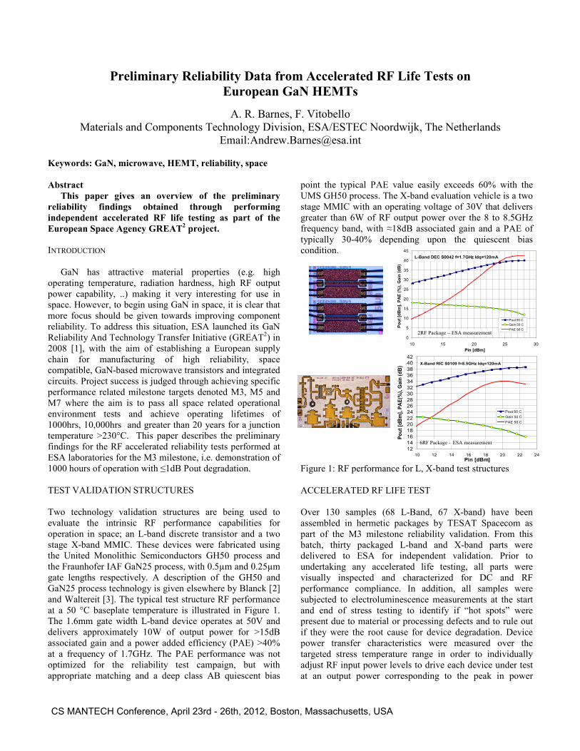
Keywords: GaN, microwave, HEMT, reliability, space Abstract This paper gives an overview of the preliminary reliability findings obtained through performing independent accelerated RF life testing as part of the European Space Agency GREAT2 project. INTRODUCTION GaN has attractive material properties (e.g. high operating temperature, radiation hardness, high RF output power capability, ..) making it very interesting for use in space. However, to begin using GaN in space, it is clear that more focus should be given towards improving component reliability. To address this situation, ESA launched its GaN Reliability And Technology Transfer Initiative (GREAT2) in 2008 [1], with the aim of establishing a European supply chain for manufacturing of high reliability, space compatible, GaN-based microwave transistors and integrated circuits. Project success is judged through achieving specific performance related milestone targets denoted M3, M5 and M7 where the aim is to pass all space related operational environment tests and achieve operating lifetimes of 1000hrs, 10,000hrs and greater than 20 years for a junction temperature >230°C. This paper describes the preliminary findings for the RF accelerated reliability tests performed at ESA laboratories for the M3 milestone, i.e. demonstration of 1000 hours of operation with ≤1dB Pout degradation. TEST VALIDATION STRUCTURES Two technology validation structures are being used to evaluate the intrinsic RF performance capabilities for operation in space; an L-band discrete transistor and a two stage X-band MMIC. These devices were fabricated using the United Monolithic Semiconductors GH50 process and the Fraunhofer IAF GaN25 process, with 0.5µm and 0.25µm gate lengths respectively. A description of the GH50 and GaN25 process technology is given elsewhere by Blanck [2] and Waltereit [3]. The typical test structure RF performance at a 50 °C baseplate temperature is illustrated in Figure 1. The 1.6mm gate width L-band device operates at 50V and delivers approximately 10W of output power for >15dB associated gain and a power added efficiency (PAE) >40% at a frequency of 1.7GHz. The PAE performance was not optimized for the reliability test campaign, but with appropriate matching and a deep class AB quiescent bias
point the typical PAE value easily exceeds 60% with the UMS GH50 process. The X-band evaluation vehicle is a two stage MMIC with an operating voltage of 30V that delivers greater than 6W of RF output power over the 8 to 8.5GHz frequency band, with ≈18dB associated gain and a PAE of typically 30-40% depending upon the quiescent bias condition.
Figure 1: RF performance for L, X-band test structures ACCELERATED RF LIFE TEST Over 130 samples (68 L-Band, 67 X-band) have been assembled in hermetic packages by TESAT Spacecom as part of the M3 milestone reliability validation. From this batch, thirty packaged L-band and X-band parts were delivered to ESA for independent validation. Prior to undertaking any accelerated life testing, all parts were visually inspected and characterized for DC and RF performance compliance. In addition, all samples were subjected to electroluminescence measurements at the start and end of stress testing to identify if “hot spots” were present due to material or processing defects and to rule out if they were the root cause for device degradation. Device power transfer characteristics were measured over the targeted stress temperature range in order to individually adjust RF input power levels to drive each device under test at an output power corresponding to the peak in power
L-Band DEC S0042 f=1.7GHz Idq=120mA
0
5
10
15
20
25
30
35
40
45
10 15 20 25 30Pin [dBm]
Pout
[dB
m],
PAE
(%),
Gai
n (d
B)
Pout 50 CGain 50 CPAE 50 C
2RF Package – ESA measurement
L-Band DEC S0042 f=1.7GHz Idq=120mA
0
5
10
15
20
25
30
35
40
45
10 15 20 25 30Pin [dBm]
Pout
[dB
m],
PAE
(%),
Gai
n (d
B)
Pout 50 CGain 50 CPAE 50 C
2RF Package – ESA measurement
X-Band RIC S0109 f=8.5GHz Idq=120mA
12141618202224262830323436384042
10 12 14 16 18 20 22 24Pin [dBm]
Pout
[dBm
], PA
E(%
), G
ain
(dB)
Pout 50 CGain 50 CPAE 50 C
6RF Package – ESA measurement
X-Band RIC S0109 f=8.5GHz Idq=120mA
12141618202224262830323436384042
10 12 14 16 18 20 22 24Pin [dBm]
Pout
[dBm
], PA
E(%
), G
ain
(dB)
Pout 50 CGain 50 CPAE 50 C
6RF Package – ESA measurement
CS MANTECH Conference, April 23rd - 26th, 2012, Boston, Massachusetts, USA
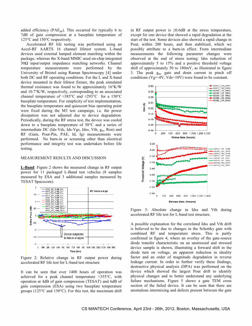
added efficiency (PAEpk). This occurred for typically 6 to 7dB of gain compression at a baseplate temperature of 125°C and 150°C respectively. Accelerated RF life testing was performed using an Accel-RF AARTS 16 channel lifetest system. L-band devices used external lumped element matching within the package, whereas the X-band MMIC used on-chip integrated 50Ω input/output impedance matching networks. Channel temperature measurements were performed by the University of Bristol using Raman Spectroscopy [4] under both DC and RF operating conditions. For the L and X-band device mounted in their lifetest fixture, the peak simulated thermal resistance was found to be approximately 16°K/W and 10.7°K/W, respectively, corresponding to an associated channel temperature of ≈385°C and ≈293°C for a 150°C baseplate temperature. For simplicity of test implementation, the baseplate temperature and quiescent bias operating point were fixed during the M3 test campaign, i.e. the power dissipation was not adjusted due to device degradation. Periodically, during the RF stress test, the device was cooled down to a baseplate temperature of 50°C and a series of intermediate DC (Ids-Vds, Ids-Vgs, Idss, Vth, gm, Ron) and RF (Gain, Pout-Pin, PAE, Id, Ig) measurements were performed. No burn-in or screening other than electrical performance and integrity test was undertaken before life testing. MEASUREMENT RESULTS AND DISCUSSION L-Band: Figure 2 shows the measured change in RF output power for 11 packaged L-Band test vehicles (8 samples measured by ESA and 3 additional samples measured by TESAT Spacecom).
Figure 2: Relative change in RF output power during accelerated RF life test for L-band test structure It can be seen that over 1400 hours of operation was achieved for a peak channel temperature >355°C, with operation at 4dB of gain compression (TESAT) and 6dB of gain compression (ESA) using two baseplate temperature groups (125°C and 150°C). For this test, the maximum drift
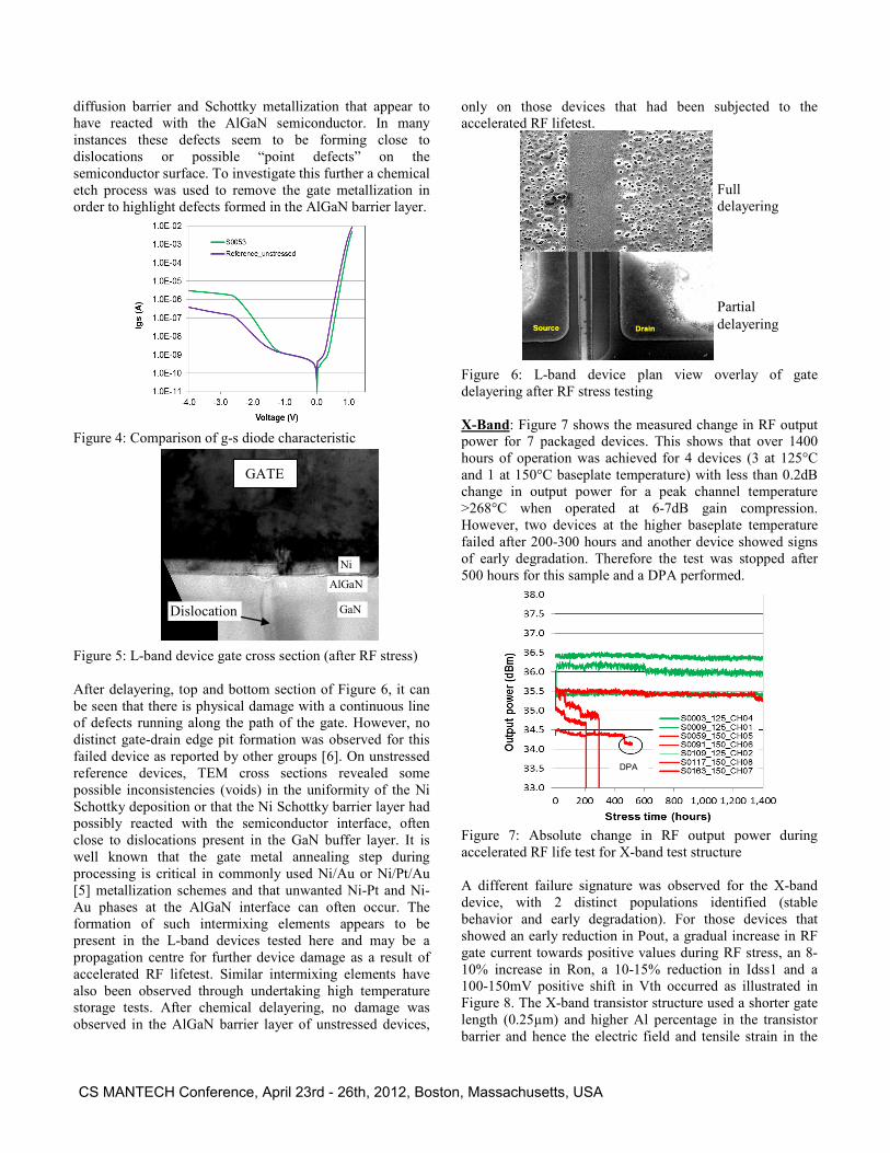
in RF output power is ≤0.6dB at the stress temperature, except for one device that showed a rapid degradation at the start of the test. Some devices also showed a rapid change in Pout, within 200 hours, and then stabilized, which we possibly attribute to a burn-in effect. From intermediate measurements the following parameter changes were observed at the end of stress testing: Idss reduction of approximately 5 to 15% and a positive threshold voltage shift of approximately 50 to 180mV, as illustrated in figure 3. The peak gm, gate and drain current in pinch off conditions (Vg=-4V, Vds=10V) were found to be constant.
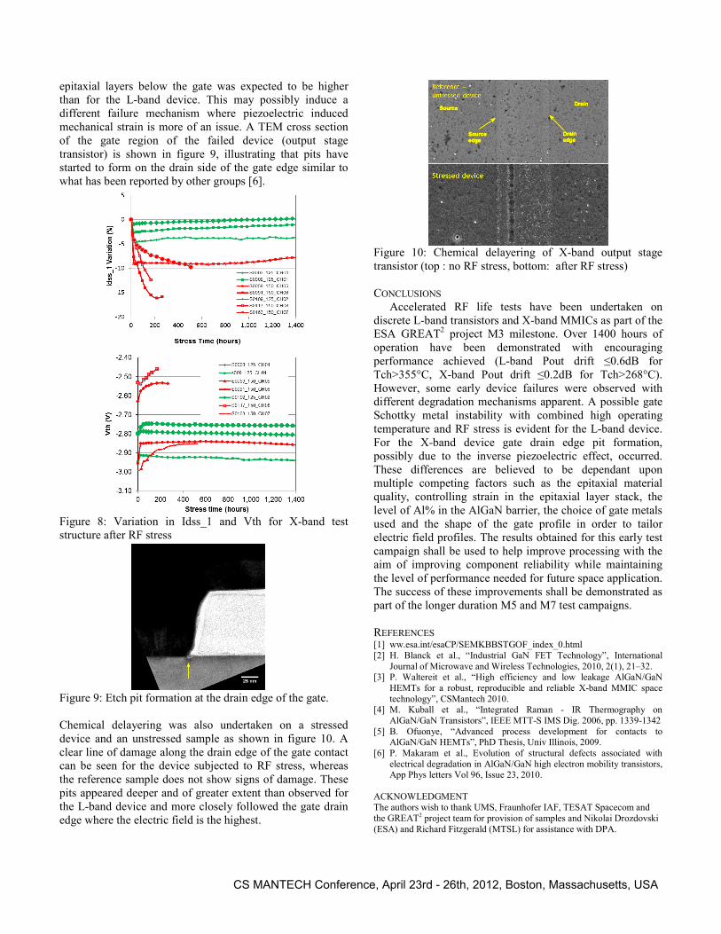
Figure 3: Absolute change in Idss and Vth during accelerated RF life test for L-band test structure. A possible explanation for the correlated Idss and Vth drift is believed to be due to changes in the Schottky gate with combined RF and temperature stress. This is partly confirmed in figure 4, where an overlay of the gate-source diode transfer characteristic on an unstressed and stressed device sample is shown, illustrating a forward shift in the diode turn on voltage, an apparent reduction in ideality factor and an order of magnitude degradation in reverse leakage current. In order to further verify these findings, destructive physical analysis (DPA) was performed on the device which showed the largest Pout drift to identify physical changes and to better understand any underlying failure mechanisms. Figure 5 shows a gate TEM cross section of the failed device. It can be seen that there are anomalous intermixing and defects present between the gate
CS MANTECH Conference, April 23rd - 26th, 2012, Boston, Massachusetts, USA
diffusion barrier and Schottky metallization that appear to have reacted with the AlGaN semiconductor. In many instances these defects seem to be forming close to dislocations or possible “point defects” on the semiconductor surface. To investigate this further a chemical etch process was used to remove the gate metallization in order to highlight defects formed in the AlGaN barrier layer.
Figure 4: Comparison of g-s diode characteristic
Figure 5: L-band device gate cross section (after RF stress) After delayering, top and bottom section of Figure 6, it can be seen that there is physical damage with a continuous line of defects running along the path of the gate. However, no distinct gate-drain edge pit formation was observed for this failed device as reported by other groups [6]. On unstressed reference devices, TEM cross sections revealed some possible inconsistencies (voids) in the uniformity of the Ni Schottky deposition or that the Ni Schottky barrier layer had possibly reacted with the semiconductor interface, often close to dislocations present in the GaN buffer layer. It is well known that the gate metal annealing step during processing is critical in commonly used Ni/Au or Ni/Pt/Au [5] metallization schemes and that unwanted Ni-Pt and Ni-Au phases at the AlGaN interface can often occur. The formation of such intermixing elements appears to be present in the L-band devices tested here and may be a propagation centre for further device damage as a result of accelerated RF lifetest. Similar intermixing elements have also been observed through undertaking high temperature storage tests. After chemical delayering, no damage was observed in the AlGaN barrier layer of unstressed devices,
only on those devices that had been subjected to the accelerated RF lifetest. Figure 6: L-band device plan view overlay of gate delayering after RF stress testing X-Band: Figure 7 shows the measured change in RF output power for 7 packaged devices. This shows that over 1400 hours of operation was achieved for 4 devices (3 at 125°C and 1 at 150°C baseplate temperature) with less than 0.2dB change in output power for a peak channel temperature >268°C when operated at 6-7dB gain compression. However, two devices at the higher baseplate temperature failed after 200-300 hours and another device showed signs of early degradation. Therefore the test was stopped after 500 hours for this sample and a DPA performed.
Figure 7: Absolute change in RF output power during accelerated RF life test for X-band test structure A different failure signature was observed for the X-band device, with 2 distinct populations identified (stable behavior and early degradation). For those devices that showed an early reduction in Pout, a gradual increase in RF gate current towards positive values during RF stress, an 8-10% increase in Ron, a 10-15% reduction in Idss1 and a 100-150mV positive shift in Vth occurred as illustrated in Figure 8. The X-band transistor structure used a shorter gate length (0.25µm) and higher Al percentage in the transistor barrier and hence the electric field and tensile strain in the
DPA
Full delayering Partial delayering
Dislocation GaN
AlGaN
Ni
GATE
CS MANTECH Conference, April 23rd - 26th, 2012, Boston, Massachusetts, USA
epitaxial layers below the gate was expected to be higher than for the L-band device. This may possibly induce a different failure mechanism where piezoelectric induced mechanical strain is more of an issue. A TEM cross section of the gate region of the failed device (output stage transistor) is shown in figure 9, illustrating that pits have started to form on the drain side of the gate edge similar to what has been reported by other groups [6].
Figure 8: Variation in Idss_1 and Vth for X-band test structure after RF stress Figure 9: Etch pit formation at the drain edge of the gate.
Chemical delayering was also undertaken on a stressed device and an unstressed sample as shown in figure 10. A clear line of damage along the drain edge of the gate contact can be seen for the device subjected to RF stress, whereas the reference sample does not show signs of damage. These pits appeared deeper and of greater extent than observed for the L-band device and more closely followed the gate drain edge where the electric field is the highest.
Figure 10: Chemical delayering of X-band output stage transistor (top : no RF stress, bottom: after RF stress) CONCLUSIONS Accelerated RF life tests have been undertaken on discrete L-band transistors and X-band MMICs as part of the ESA GREAT2 project M3 milestone. Over 1400 hours of operation have been demonstrated with encouraging performance achieved (L-band Pout drift ≤0.6dB for Tch>355°C, X-band Pout drift ≤0.2dB for Tch>268°C). However, some early device failures were observed with different degradation mechanisms apparent. A possible gate Schottky metal instability with combined high operating temperature and RF stress is evident for the L-band device. For the X-band device gate drain edge pit formation, possibly due to the inverse piezoelectric effect, occurred. These differences are believed to be dependant upon multiple competing factors such as the epitaxial material quality, controlling strain in the epitaxial layer stack, the level of Al% in the AlGaN barrier, the choice of gate metals used and the shape of the gate profile in order to tailor electric field profiles. The results obtained for this early test campaign shall be used to help improve processing with the aim of improving component reliability while maintaining the level of performance needed for future space application. The success of these improvements shall be demonstrated as part of the longer duration M5 and M7 test campaigns. REFERENCES [1] ww.esa.int/esaCP/SEMKBBSTGOF_index_0.html [2] H. Blanck et al., “Industrial GaN FET Technology”, International
Journal of Microwave and Wireless Technologies, 2010, 2(1), 21–32. [3] P. Waltereit et al., “High efficiency and low leakage AlGaN/GaN
HEMTs for a robust, reproducible and reliable X-band MMIC space technology”, CSMantech 2010.
[4] M. Kuball et al., “Integrated Raman - IR Thermography on AlGaN/GaN Transistors”, IEEE MTT-S IMS Dig. 2006, pp. 1339-1342
[5] B. Ofuonye, “Advanced process development for contacts to AlGaN/GaN HEMTs”, PhD Thesis, Univ Illinois, 2009.
[6] P. Makaram et al., Evolution of structural defects associated with electrical degradation in AlGaN/GaN high electron mobility transistors, App Phys letters Vol 96, Issue 23, 2010.
ACKNOWLEDGMENT The authors wish to thank UMS, Fraunhofer IAF, TESAT Spacecom and the GREAT2 project team for provision of samples and Nikolai Drozdovski (ESA) and Richard Fitzgerald (MTSL) for assistance with DPA.
CS MANTECH Conference, April 23rd - 26th, 2012, Boston, Massachusetts, USA