perovskites for ultrafast active terahertz photonics
TRANSCRIPT

This document is downloaded from DR‑NTU (https://dr.ntu.edu.sg)Nanyang Technological University, Singapore.
Perovskites for ultrafast active terahertzphotonics
Kumar, Abhishek
2020
Kumar, A. (2020). Perovskites for ultrafast active terahertz photonics. Doctoral thesis,Nanyang Technological University, Singapore.
https://hdl.handle.net/10356/145567
https://doi.org/10.32657/10356/145567
This work is licensed under a Creative Commons Attribution‑NonCommercial 4.0International License (CC BY‑NC 4.0).
Downloaded on 18 Mar 2022 19:23:09 SGT

1
[PEROVSKITES FOR ULTRAFAST ACTIVE TERAHERTZ
PHOTONICS]
[ABHISHEK KUMAR]
SCHOOL OF PHYSICAL AND MATHEMATICAL SCIENCES
[2020]

2
[PEROVSKITES FOR ULTRAFAST ACTIVE TERAHERTZ
PHOTONICS]
[ABHISHEK KUMAR]
SCHOOL OF PHYSICAL AND MATHEMATICAL SCIENCES
A thesis submitted to the Nanyang Technological University
in partial fulfilment of the requirement for the degree of
Doctor of Philosophy
2020

3
Statement of Originality
I hereby certify that the work embodied in this thesis is the result of original research done by me
except where otherwise stated in this thesis. The thesis work has not been submitted for a degree
or professional qualification to any other university or institution. I declare that this thesis is
written by myself and is free of plagiarism and of sufficient grammatical clarity to be examined.
I confirm that the investigations were conducted in accord with the ethics polices and integrity
standards of Nanyang Technological University and that the research data presented honestly and
without prejudice.
23-11-2020 Abhishek Kumar
Date Input Name Here

4
Supervisor Declaration Statement
I have reviewed the content and presentation style of this thesis and declare it of sufficient
grammatical clarity to be examined. To the best of my knowledge, the thesis is free of plagiarism
and the research and writing are those of the candidate’s except as acknowledged in the Author
Attribution Statement. I confirm that the investigations were conducted in accord with the ethics
policies and integrity standards of Nanyang Technological University and that the research data
are presented honestly and without prejudice.
23-11-2020 Assoc. Prof Ranjan Singh
Date Input Supervisor Name Here
5
Authorship Attribution Statement
The thesis contains material from 3 papers published in the following peer-
reviewed journal where the author’s contributions are listed below:
Chapter 3 is published as Manu Manjappa, Ankur Solanki, Abhishek Kumar, Tze Chien Sum,
and Ranjan Singh, "Solution-Processed Lead Iodide for Ultrafast All-Optical Switching of
Terahertz Photonic Devices,” Advanced Materials, vol. 31, no. 32, p. 1901455, 2019, doi:
10.1002/adma.201901455.
The contributions of the authors are following:
• Manukumara Manjappa and I performed the experiments and done the terahertz
characterization.
• Manukumara Manjappa and I fabricated the metamaterial samples.
• Ankur Solanki has done the perovskite thin film fabrication, characterization and
deposition on metamaterial samples.
• Prof Ranjan Singh and Prof Tze Chien Sum supervised the whole project and edited the
manuscript drafts.
Chapter 4 is published as Abhishek Kumar, Ankur Solanki, Manukumara Manjappa, Sankaran
Ramesh, Yogesh Kumar Srivastava, Piyush Agarwal, Tze Chien Sum and R. Singh, "Excitons in
2D perovskites for ultrafast terahertz photonic devices," Science Advances, vol. 6, no. 8, p.
eaax8821, 2020, doi: 10.1126/sciadv. aax8821.
The author’s contributions are following:
• Abhishek Kumar, Ankur Solanki, Prof Ranjan Singh and Prof Tze Chien Sum
conceived the idea.
• Abhishek Kumar designed the experiments and performed all the terahertz
measurements and theoretical analysis.
• Yogesh and Abhishek fabricated the metamaterial samples.
• Ankur Solanki prepared all the perovskite thin films and performed the characterization
• Sankaran Ramesh performed the transient PL measurement.
• Abhishek, Manu and Piyush performed the analysis in THz measurements.
• Prof Ranjan Singh and Prof Tze Chien Sum supervised the overall work.
• Abhishek wrote the manuscript drafts and all other co-authors provided their feedback
to improve it.
Chapter 5 is published as Abhishek Kumar, Anish Priyadarshi, Sudhanshu Shukla, Manukumara
Manjappa, Lew Jia Haur, Subodh G Mhaisalkar, Ranjan Singh, "Ultrafast THz photophysics of

6
solvent engineered triple-cation halide perovskites,” Journal of Applied Physics, vol. 124, no.
21, p. 215106, 2018, doi: 10.1063/1.5051561.
The author’s contributions are mentioned below:
• Abhishek Kumar Prof Ranjan Singh conceived the idea.
• Abhishek Kumar performed the THz measurements and performed the analysis with the
help of Manukumara Manjappa.
• Anish Priyadarshi, Sudhanshu Shukla and Lew Jia Haur prepared the perovskite
samples and done the characterization of film quality.
• Prof Ranjan Singh and Prof Subodh G. Mhaisalkar supervised the overall project.
• Abhishek Kumar wrote the manuscript with the inputs from all other co-authors.
23-11-2020 Abhishek Kumar
Date Input Name here

7
Abstract
In the electromagnetic spectrum terahertz (THz) frequency that lies between
conventional electronics and photonics is vital due to its uniqueness and high
potential for many disruptive applications such as security, high-resolution
imaging, ultrasensitive sensors and high-speed wireless communication for the
sixth generation (6G). THz waves hold the potential to boost the key performance
of many existing technologies thus, the emergence of THz photonics is inevitable.
Hence, it is of paramount importance to develop the technology that provides
unprecedented control on terahertz waves. The difficulties to control the
properties of THz waves using natural existing materials led to the development
of artificial composite materials known as metamaterial (MM).
Metamaterial (MM) offers a simple and effective platform to develop the terahertz
technologies owing to its scalable and on demand optical property that could be
tuned. Active control of metamaterial response enables realization of THz
functional devices. More importantly, the ability to control THz waves at ultrafast
time scale is extremely crucial for developing next generation high-speed wireless
communication. Integrating dynamic material such as semiconductors with MM
offers a possible solution. However, for commercial large-scale deployment a
cost-effective high performing functional solution is desired for advance
manipulation of THz waves in emerging THz technologies.
This thesis aims to address these questions and provides a possible route to
develop cost effective, easily integrable and high performing ultrafast THz
photonic devices by integrating solution processed perovskite with metallic THz
8
metamaterial (MM) structures. In the development of ultrafast active THz devices,
the natural progression is to introduce multifunctionalities in active metamaterial
for advance manipulation of THz waves. In this context, strong interaction of
perovskite thin film with confined THz electric field offers a viable route to tune
the carrier dynamics which is key to the foundation for next generation
multifunctional active metamaterials.
In this thesis, solution processed perovskite has been explored to develop ultrafast
THz photonics device. Fano resonant metamaterial structures owing to strong THz
electric field confinement were employed to integrate with perovskites. The high
photoconductivity and ultrafast free carrier dynamics in perovskite thin film
enabled near unity modulation of THz electric field at ultrafast timescale. The
existence of self-assembled quantum well (QW) in 2D perovskite provides an
additional channel for the photoexcited free carrier to relax at ultrafast time scales
(~ 20 ps) which is fastest in the family of solution processed semiconductors. We
demonstrated 2D perovskite integrated hybrid metadevice at rigid as well as
flexible platform that showed modulation of THz waves at ~ 50 GHz modulation
speed.
In the future prospect of the thesis we provide an outlook to achieve wavelength
dependent response of active THz metadevice through integration of perovskites
with silicon. The large band gap tunability, ease of integration and ultrafast carrier
dynamics of perovskite opens a new paradigm to develop multifunctional ultrafast
active THz photonic devices for advance manipulation of THz waves.

9
Acknowledgements
First and foremost, I would like to express my sincere gratitude to my supervisor Prof
Ranjan Singh for his continuous encouragement and unwavering support and trust on me.
I was blessed to have his continuous guidance and immense support in all possible means
throughout my PhD journey. He facilitated all the resources and his valuable time for
discussions at any time whenever needed. He has taught me the value of hard work,
discipline and dedication that will help me in all the ways of my life. I would also like to
acknowledge my thesis advisory committee members Prof Cesare Soci and Prof Shuzhou
Li for their critical evaluation and suggestions throughout my PhD journey. I would like
to thank Prof Tze Chien Sum for his valuable discussion and guidance.
I would like to thank all faculty members and admin staffs of our centre CDPT (Centre
for disruptive photonic technologies) for providing state-of-the art facilities and
competitive research ambience. The weekly organized CDPT meetings not only allowed
to learn the research works from other people but also helped me to shape idea in a better
way from the constructive criticism of CDPT members.
I deeply thank to all my lab members for all the wonderful times that made the PhD
journey easy. It has been a great pleasure to work with all the lab members. You guys
were always there for discussion. Whenever I needed any help in experiments, simulation
and fabrications you guys helped me a lot in every sense. I extend my sincere thanks to
Manu, Prakash, Yogesh, Manoj, Piyush, Thomas, Yi Ji, Song Han and Sreekanth for their
encouragement and fruitful discussion. Especially, I would like to thank Manu who
mentored throughout my PhD journey. I learnt a lot from you either it is experimental
skill or writing a research article. I would also like to thank Prakash who taught me how
to frame an idea and be professional. I always get new perspectives after discussing with
you either it is scientific or non-scientific topics.
None of this would have been possible without the love and support of my family. I
cannot thank enough my Mummy and Daddy, who always have given me the freedom to
make my decisions for life. Both of you guys always understand me without even saying
any words. Your encouragement and mental support always helped me to handle the ups
and down of my PhD journey. I am blessed to have siblings like Golu and Sweety. I
cannot thank enough to both of you for your constant support and involvement any day,
anytime.
The list of acknowledgements is incomplete if I won’t include my friends. Mayank,
Raghav, Shubham chetta, Subrata, Rahul and Anand. It is not less than blessing to have
friends like you. Right from IISER to throughout the PhD journey it’s not easy to
maintain the true friendship. Despite of having time differences you guys were always
there for moral support and all the fun discussions. I would also like to thank my flat

10
mates Durgesh, Udvas, Piyush and Poulomi. Because of you guys it was bit easy to spend
time away from family. Celebrating each other’s birthday and our festivals compensated
the missing of families. I must say having you guys were very important which never
isolated me in my PhD journey.
I would like to thank the most special person, Dipa, for her constant support and always
being there for me any day and anytime. Thank you for always keep me motivated. I
cannot thank enough to you in words. It is not less than blessing to have you in this
journey. Your enthusiasm towards work and immense amount of dedication always keep
me motivated. I learnt a lot from you and my perspective towards life became more
positive.

11
Chapter 1 .................................................................................................................................. 13
Introduction: Theory and Overview ....................................................................................... 13
1. 1 Why terahertz frequencies are important: A motivation behind closing the “terahertz
gap” ................................................................................................................................... 14
1.2 A brief history of THz technologies .............................................................................. 16
1.3 Metamaterial ................................................................................................................ 19
1.4 Metamaterial: A perfect platform for THz .................................................................... 28
1.5 Research gap in active THz photonics and motivation of the thesis............................... 29
1.6 Fano resonance in terahertz metamaterials .................................................................... 30
1.7 Dynamic metamaterial in THz frequency ..................................................................... 34
1.9 Why Perovskite for THz applications? ......................................................................... 38
1.10 Scope of the thesis ...................................................................................................... 39
1.11 References .................................................................................................................. 42
Chapter 2 .................................................................................................................................. 46
Simulation, Characterization technique and Fabrication ......................................................... 46
2.1 Electromagnetic Simulation of terahertz metamaterial .................................................. 46
2.2 Terahertz time domain spectroscopy (THz-TDS) .......................................................... 55
2.3 Optical Pump Terahertz Probe spectroscopy (OPTP) .................................................... 66
2.4 Sample fabrication ....................................................................................................... 68
2.5 References.................................................................................................................... 70
Chapter 3 .................................................................................................................................. 73
Solution-processed Lead iodide for Ultrafast Terahertz Photonic devices............................... 73
3.1 Introduction .................................................................................................................. 73
3.2 Terahertz time resolved spectroscopy (TRTS) of PbI2 thin film .................................... 76
3.3 PbI2 integrated hybrid metadevice ................................................................................ 78
3.4 Effect of thickness on ultrafast dynamics ...................................................................... 88
3.5 References.................................................................................................................... 91
Chapter 4 .................................................................................................................................. 93
Excitons in 2D perovskites for ultrafast terahertz photonic devices ........................................ 93
4.1 Introduction .................................................................................................................. 93
4.2 Structural and optical characterization of 2D perovskite thin film ................................. 96
12
4.3 Integration of 2D perovskite with metamaterial .......................................................... 106
4.4 Active flexible metadevice ......................................................................................... 114
4.5 References.................................................................................................................. 119
Chapter 5 ................................................................................................................................ 122
Ultrafast THz photo physics of solvent engineered triple-cation halide perovskite ............... 122
5.1 Introduction ................................................................................................................ 122
5.2 Why mixed cation perovskite?.................................................................................... 123
5.3 Optical pump terahertz probe (OPTP) of mixed cation/anion perovskite ..................... 123
5.4 References.................................................................................................................. 130
Chapter 6 ................................................................................................................................ 133
Conclusion and Future direction .......................................................................................... 133
6.1 Future works .............................................................................................................. 135
6.2 References.................................................................................................................. 139
Appendix A ......................................................................................................................... 140

13
Chapter 1
Introduction: Theory and Overview
The remarkable properties of electromagnetic waves have led the development of many
disruptive technologies and changed the life in an unimaginable way. This has always motivated
to develop a platform that provides unprecedented control on the electromagnetic waves. In the
EM spectrum, “terahertz (THz)” which lies between the electronics and photonics realm was
largely unexplored due to the lack of the natural material that responds to the THz region. At
lower frequencies (less than a few hundred of GHz), the motion of free electrons characterizes
the EM devices, and generally known as electronics. The output power of EM waves decreases
with increasing the frequencies as a consequence of mainly following factors: (i) carriers
saturation velocity, that typically falls in the range of 105 m/s (ii) maximum electric field
supported by the device before breakdown. These majorly limits the source power to sub-
milliwatt level for 300 GHz and few microns level for frequencies near to 1 THz[1]. While on the
other hand, the photonics realm of EM spectrum that spans optical and ultra-violet wavelength
region shows a decrease in output power with a decrease in frequencies. The main reason behind
this is the lack of natural materials that satisfy the bandgap requirement for photonic sources. In
contrast, the terahertz electric field oscillations are too fast for conventional high-speed
electronics devices to respond and at the same time their energy is too low to provide efficient
photonics devices. This has hindered the technological advancement in terahertz technologies for
14
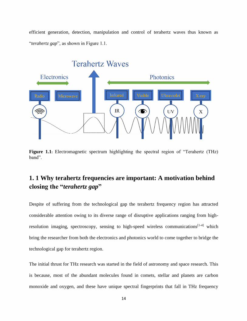
efficient generation, detection, manipulation and control of terahertz waves thus known as
“terahertz gap”, as shown in Figure 1.1.
Figure 1.1: Electromagnetic spectrum highlighting the spectral region of “Terahertz (THz)
band”.
1. 1 Why terahertz frequencies are important: A motivation behind
closing the “terahertz gap”
Despite of suffering from the technological gap the terahertz frequency region has attracted
considerable attention owing to its diverse range of disruptive applications ranging from high-
resolution imaging, spectroscopy, sensing to high-speed wireless communications[1-4] which
bring the researcher from both the electronics and photonics world to come together to bridge the
technological gap for terahertz region.
The initial thrust for THz research was started in the field of astronomy and space research. This
is because, most of the abundant molecules found in comets, stellar and planets are carbon
monoxide and oxygen, and these have unique spectral fingerprints that fall in THz frequency

15
region[5]. Slowly, THz spectroscopy became an important tool for material characterization
owing to its noninvasive and low photon energy (~ 4.1 meV) nature. THz time-domain
spectroscopy (THz-TDS) has been intensively employed to unravel the carrier dynamics of many
important materials like 2D materials (graphene, WSe2, MoS2), high-temperature
superconductor and semiconductors (GaAs, perovskites, Ge and many more)[6-8]. The ability to
capture directly both the amplitude and phase at individual frequencies in THZ-TDS without
employing Kramers-Kronig relation allows to extract the frequency dependent complex optical
constants of materials.
As THz waves can penetrate most dielectric and non-polar liquids thus it is very useful for
applications like security screening, food and pharmaceutical quality control monitoring, and
medical diagnosis[1, 9]. Its harmless interaction with human tissue owing to low photon energy (in
the range of meV) has allowed the use of THz waves for a wide range of applications such as
skin cancer detection, bio and drug detection.
In recent years information and communication technology (ICT) has been seen to be benefited
by terahertz technology due to the availability of huge spectral bandwidth that offers high-speed
wireless communication, high volume data processing, and satellite communication[3, 10]. THz
frequency has been envisioned as the next frontier for high-speed wireless communication for
beyond 5G communication: 6G communication[11, 12]. With the current implementation of 5G
networks underway, the pursuit for 6G wireless communication has already begun. 6G wireless
communication is expected to provide terabit per second (Tbps) data rates, which will lead to
novel applications such as a fully connected cyber-physical world (internet of everything),
wireless data centers, massively multicore processors, and will foster the Industry 4.0 revolution.
Carrier waves operating at THz frequencies are vital for achieving the desired data rates of 6G
16
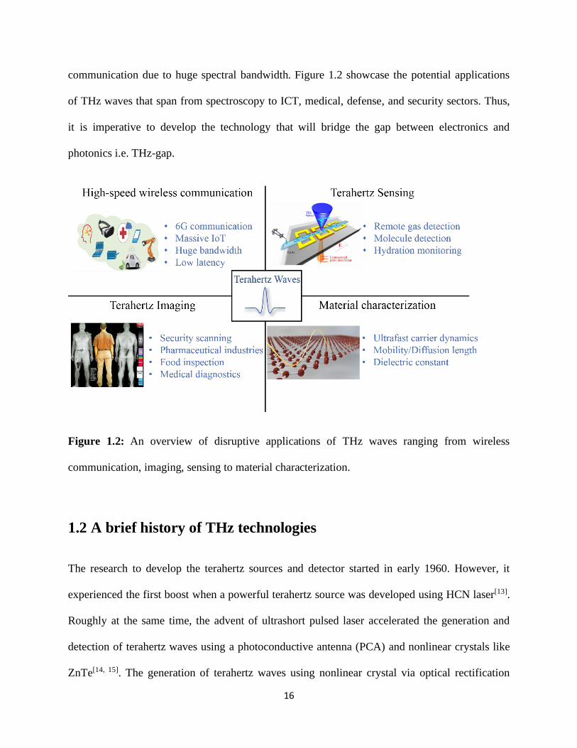
communication due to huge spectral bandwidth. Figure 1.2 showcase the potential applications
of THz waves that span from spectroscopy to ICT, medical, defense, and security sectors. Thus,
it is imperative to develop the technology that will bridge the gap between electronics and
photonics i.e. THz-gap.
Figure 1.2: An overview of disruptive applications of THz waves ranging from wireless
communication, imaging, sensing to material characterization.
1.2 A brief history of THz technologies
The research to develop the terahertz sources and detector started in early 1960. However, it
experienced the first boost when a powerful terahertz source was developed using HCN laser[13].
Roughly at the same time, the advent of ultrashort pulsed laser accelerated the generation and
detection of terahertz waves using a photoconductive antenna (PCA) and nonlinear crystals like
ZnTe[14, 15]. The generation of terahertz waves using nonlinear crystal via optical rectification
17
started in 1970’s. Later between 1975-82 the generation of terahertz was demonstrated using
Auston switch. It was the combination of ultrashort pulsed laser and electrooptic sampling which
opened up a new spectroscopic modality, terahertz time domain spectroscopy (THz-TDS) in
1989[16].
The success of semiconductor-based laser in the visible and near-infrared frequency region has
always motivated the researcher to develop similar technology for THz frequencies. However,
the lack of appropriate interband materials pushed the researcher to develop an artificially
engineered material that could generate THz waves. The pursuit of developing efficient
THz sources led to the first demonstration of quantum cascade laser (QC) in 1988[17, 18]. This was
one of the remarkable discoveries that boosted THz research activities. Since then significant
research has been done in the development of QC lasers. Currently, the QC laser has a broad
frequency range of operation that can emit THz waves from 0.8-5 THz[19]. However, one of the
major problems with QC laser was its inability to operate at room temperature. That prevented
the QC lasers from finding the place directly into the commercial applications. But owing to its
high resolution spectral and high output power many investigations even in recent time going to
improve the functionality. For example, the recent work in 2012 has shown the operation of QC
laser at 200 K[20]. Very recently the topological Valley Hall crystal-based THz QC has been
demonstrated where the topologically protected Valley Hall cavity has been utilized which is
more robust and immune from back scattering[21]. Despite of not being operating at room
temperature, the future of QC laser is healthy. It is still a high power (> 1W)[22] THz source that
serves many applications such as high-resolution imaging[23-25].

18
The potential of terahertz waves for wireless communication was first demonstrated by Gebbie
in 1970. It was the lack of appropriate source, detector, and modulators that halted the
application of terahertz waves for wireless communication. However, looking at the current trend
of data consumption, particularly in the wireless domain, there is a huge demand to develop a
wireless system that could support tens to hundreds of gigabits per second. To accommodate this
demands the obvious route is to increase the carrier frequency towards a higher node. The
current 5G communication is using up to 100 GHz as a carrier frequency. But 5G is not an
ultimate solution to communicate the gigantic volume of data at a near-instant time scale. Thus,
for the next generation wireless communication: i.e. 6G communication, the terahertz wave is
inevitable. Hence, foreseeing the bright future of terahertz-based communication, global intense
research effort has been started in recent few years. Researchers have taken photonics-based
route to demonstrate the high-speed terahertz wireless communication[3, 10, 26]. In this approach
uni traveling carrier photodiode (UTC-PD) is employed as a THz source. The added advantage
with the photonics-based approach is that a mature developed modulation technology can be
used to implement an advanced modulation scheme for the THz wireless communication. To
showcase the potential of THz waves for high-speed wireless communication a photonics-based
THz wireless system with an operating frequency 120 GHz has been successfully demonstrated
data transmission of 4K video streaming at a distance of 100 m[27, 28]. Also, the recent
development in semiconductor IC technologies allowed to develop the low cost, miniaturized
terahertz system that brings the terahertz technologies one step closer towards consumer
operation[29, 30]. In this direction, the electronics-based source like resonant tunneling diode
(RTD) is viable that can emit terahertz waves with output power up to 1 mW. The development
of RTD has opened up a new avenue for portable terahertz sources that could easily integrate
19
with existing silicon-based technologies. In summary, the journey of terahertz technologies is
witnessing rapid development that is inspired and accelerated by its disruptive applications.
These technological advancements will bridge the gap between electronics and photonics which
is known as “terahertz gap”
1.3 Metamaterial
Metamaterial, an artificially engineered structure with exotic and tunable materials properties has
emerged as a new frontier of science involving physics, chemistry engineering, and material
science. The advent of metamaterials has opened a new paradigm for controlling electromagnetic
waves. Just after the first experimental demonstration of metamaterials, the scientific community
quickly realized that the potential of metamaterials is unprecedented.
In general, the property of bulk material is essentially derived from its chemical elements. People
have always intended to control and tune the optical properties of materials. For instance, slight
doping of silicon enhances the conductivity by an order of magnitudes that led to the foundation
of the whole semiconductor industry. Similarly, the recent nanoscience and technology have
always targeted to better understand the material properties starting from the atom to the
molecule level. All these efforts have been put to enhance the applications using materials.
In this context, metamaterial emerged as a new frontier for technologies. It offered an entirely
new route to further enhance the capability to design the material properties at will. As
compared to natural existing materials, the physical and optical properties of metamaterials are
not primarily dependent on chemical compositions rather it derives its properties from the
geometry of meta-atoms.

20
1.3.1 A brief history of metamaterial
The root of “artificial materials or metamaterials” can be found in 1898 when Jagadish Chandra
Bose showed the polarization of microwaves using the twisted jute[31]. Then after a decade in
1914, Lindman showed an “artificial chiral materials” [32]. The concept of negative refractive
index came after a long pause.
It was Veselago’s seminal work that again created the noise about metamaterials. In his seminal
work, he showed the theoretical overview of left-handed materials (LHM). LHM is characterized
as a material having simultaneous negative value of permittivity (ɛ) and permeability (μ). He
showed a systematic analysis of the behavior of electromagnetic waves in LHM, that predicted
exotic features like backward Cerenkov radiation and reversed Doppler shift[33].
Despite of having theoretical framework for LHM, the works of Veselago and others went
unnoticed for almost 30 years due to the lack of experimental evidence. It was Sir John Pendry,
who demonstrated negative permittivity (ɛ) and permeability (μ). The demonstration of negative
permittivity came in 1996 using a thin wire medium, followed by the demonstration of negative
permeability in 1999 by using the well-known split ring resonator (SRR) as magnetic element[34,
35]. Using both the concepts of negative ɛ and μ, in 2000 Smith et al. experimentally showed the
first negative refractive index artificial material[36].
Since then, the research in metamaterial has seen an unprecedented rise. Many exotic phenomena
have been shown such as negative refractive[37-40] , super-lensing[41-43], cloaking[44, 45] , perfect
absorbers[46, 47] and transformation materials[48, 49]. However, all these pioneering works are based
on passive metamaterials. Although, passive metamaterials have provided a route to engineer the
optical properties of materials on demand, but their dynamic tunability is missing. For many
21
potential applications the dynamic control on the material properties is desirable that has given
the birth of “active metamaterial”.
In the quest of developing active metamaterial, the first work came in 2006, where Padilla et al.
[50] demonstrated dynamic control of electric response of SRR through photoexcitation of free
carriers in the substrate. Followed by this Chen et al.[51] showed electrical control of terahertz
metamaterials using electric biasing. Since then, the field of active metamaterials has seen rapid
growth and expanded the horizon of metamaterials applications. In active metamaterial most of
the work includes the dynamic control by means of optical, electrical, thermal and mechanical [8,
50-52]. Each has their own advantages and limitations. For the development of ultrafast devices,
the optical control is viable as it provides fast tunability.
1.3.2 Overview of metamaterial
In general, the isotropic materials are characterized by their effective permittivity (ɛ) and
permeability (μ), where ɛ contains the properties corresponds to electric field while μ
corresponds to magnetic field. The ɛ and μ of most of the natural materials are defined with
reference to free space as: ɛ𝑟 =ɛɛ0⁄ and μ𝑟 =
μμ0⁄ , where ɛ𝑟 and μ𝑟 are the relative permittivity
and permeability of material respectively, ɛ0 and μ0 are the free space permittivity and
permeability respectively. The refractive index of material can be written as: 𝑛 = √ɛ𝑟 μ𝑟 . Figure
1.5 shows the classification of isotropic materials based on their ɛ and μ in the ɛ - μ space. The
first quadrant characterizes as positive ɛ and μ. Most of the natural existing dielectric materials
fall in this region. They are also called as right-handed material (RHM). According to Maxwell’s
equation the electric field E, the magnetic field H, and the propagation direction k form right-
handed triplet as shown in Figure 1.5. The second quadrant characterizes as negative permittivity

22
(ɛ < 0) and positive permeability (μ > 0). Most of the plasmonic materials such as gold (Au),
silver (Ag) in visible and ultra-violet frequencies fall in this region. The materials fall in this
region support evanescent decay fields. The third quadrant which characterizes as ɛ < 0 and μ < 0
is known as left-handed material (LHM) that supports many exotic phenomena such as negative
refractive index, backward propagating waves, and many more. No known natural materials fall
in this quadrant. The artificially engineered materials by selectively designing the permittivity
and permeability to negative value lie in this quadrant. For this quadrant, the triplet E-H-k
follow left-hand rule. The fourth quadrant (ɛ > 0 and μ < 0) is known as magnetic plasma, which
supports evanescent waves. Only few ferromagnetic materials at sub-GHz frequencies fall in this
region.
Figure 1.3: Material parameters space characterized by permittivity (ɛ) and permeability (μ).
23
After looking at the classifications of materials based on their ɛ and μ, we talk about a new form
of material: metamaterial. A metamaterial (MM) is an artificially designed material that attains
its properties from its sub-wavelength sized unit structure rather than its constituent materials.
The sub-wavelength sized unit cell is called as “meta-atoms”. The meta-atoms of MM are
typically arranged in the periodic fashion on dielectric substrate. As depicted in Figure 1, the
periodicity of meta-atoms is much smaller than the wavelength of the incident light, thus
allowing the incoming light to see the MM system as an effective homogeneous medium. The
total electromagnetic response from the MM system is considered as collective response of the
constituent unit cells. Thus, by tuning the geometrical parameters of the unit cell, the EM
response of MM can be tuned. This remarkable feature of MM allowed to realize many exotic
electromagnetic phenomena such as negative refractive index and inverse Doppler shift.
The EM response of MM is characterized by effective permittivity and permeability which is
derived from the homogenization of the sub-wavelength structures by averaging the local
fields[53, 54]. At the early days, negative-refractive index material or LHM used to be considered
as metamaterials as predicted by Vesalago in 1968[33]. In contrast, the material falls in the third
quadrant of Figure 1.5 used to be considered as metamaterial. But nowadays, the term
metamaterial is used not only to address the LHM rather it has a much broader scope than LHM.
In a more general way, any artificial EM materials that derive its optical properties like ɛ and μ
from the constituent periodic inclusions are referred as metamaterial. Thus, for the classification
shown in Figure 1.5, today metamaterials denote any artificial effective medium that can belong
in any of the second, third and fourth quadrant.
24
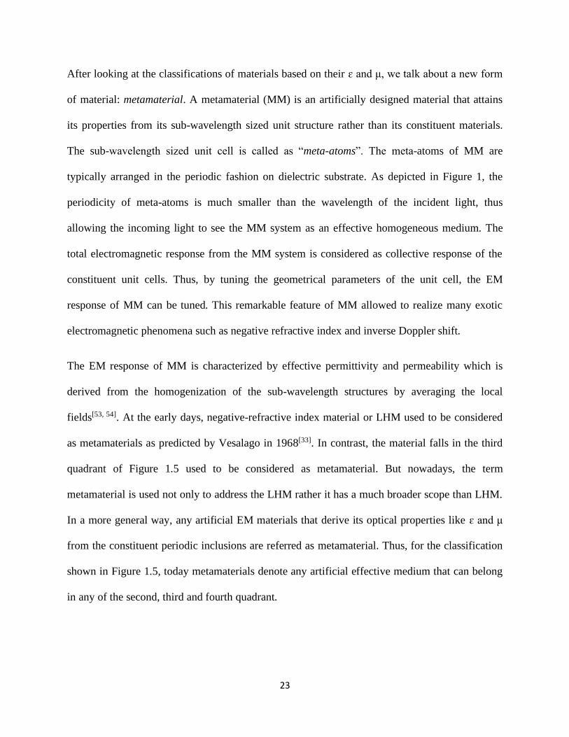
Figure 1.4 Periodic arrangement of metamaterial (MM) array illustrating the periodicity (p) is
much less than the wavelength of incident EM waves. Inset shows the unit cell of MM, where l is
the side length, w is the width and g are the width of gap.
Next, we talk about the two most common types of unit cells that comprise metamaterials and
allow to demonstrate negative ɛ and μ. These are magnetic split ring resonator (mSRR) and
electric split ring resonator (eSRR). By changing the geometrical parameters of these unit cells,
the range of operating frequency can be tuned.
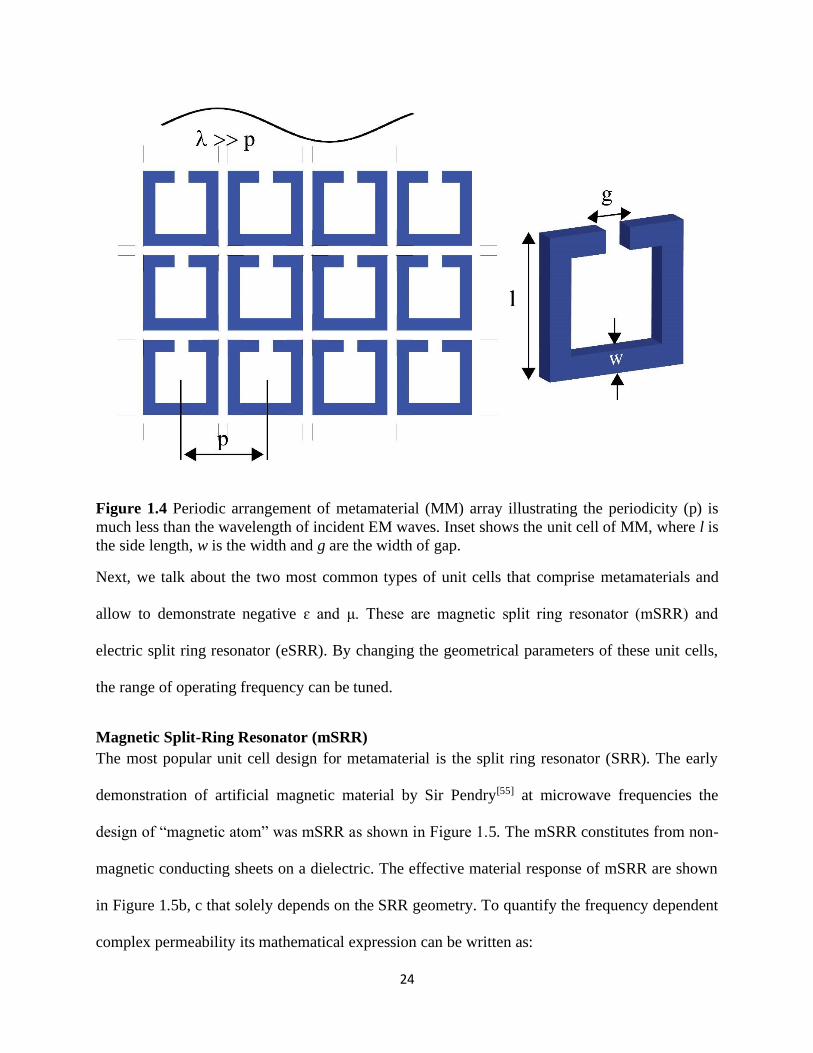
Magnetic Split-Ring Resonator (mSRR)
The most popular unit cell design for metamaterial is the split ring resonator (SRR). The early
demonstration of artificial magnetic material by Sir Pendry[55] at microwave frequencies the
design of “magnetic atom” was mSRR as shown in Figure 1.5. The mSRR constitutes from non-
magnetic conducting sheets on a dielectric. The effective material response of mSRR are shown
in Figure 1.5b, c that solely depends on the SRR geometry. To quantify the frequency dependent
complex permeability its mathematical expression can be written as:

25
μ𝑒𝑓𝑓 = 1 +
𝐹 𝜔2
𝜔02 − 𝜔2 − 𝑖𝛾𝜔
= μ𝑒𝑓𝑓1 + 𝑖μ𝑒𝑓𝑓
2 (1.1)
where, ω0 is the resonant frequency, F and γ are geometrical and damping constants respectively.
To quantify the resonance strength the quality factor (Q) is defined as 𝑄 = 𝜔0
𝛾 where γ
characterizes the bandwidth of the resonance. From equation 1, it is clear that at high Q of the
resonator near the vicinity of 𝜔0 the real part of μ𝑒𝑓𝑓 will be negative. To get more intuitive
picture, we consider mSRR as inductor-capacitor (LC) resonator, where the inductance (L) arises
from the circulating current in the periphery of mSRR and capacitance (C) comes from the
dielectric gap of the split ring. The resonance frequency of the SRR can be given as 𝜔0 =
√1 𝐿𝐶⁄ . When a time varying magnetic field polarized perpendicular to the plane of mSRR is
incident (Figure 1.5a), it induces a circulating current that causes accumulation of charges with
opposite polarity at the split gap. This induces strong field confinement across the split gap as
shown in Figure 1.5e. Below the resonant frequency, ω0, the currents in the loop are in phase
with the incident field that results in a positive response that also manifests as positive
permeability (μ). But at the proximity of resonant frequency, ω0, the currents in the loop lag thus
results as negative response that manifests as negative value of permeability (μ).
26
Figure 1.5 Split ring resonator (SRR) (a) Array of SRR with periodicity is much less than (a ~
λ0/10) the wavelength of incident EM wave. (b) Reflection (red solid line) and transmission
(black solid line) spectra from the SRR (c) The extracted and simulated magnetic response of the
SRR (d) Surface current distribution at resonant frequency (e and f) Simulated electric and
magnetic field distributions at resonant frequency.
Electrical Split Ring Resonator (eSRR)
Figure 1.6 shows the most common eSRR. The frequency dependent permittivity of natural
occurring material can be written using Drude-Lorentz relation:
ɛ𝑒𝑓𝑓 = 1 −
𝜔𝑝2
𝜔2 − 𝜔0 2 − 𝑖𝛾𝜔
(1.2)
where, ωp is the plasma frequency given by
𝜔𝑝2 =
4𝜋𝑛𝑒2
𝑚∗
(1.3)

27
here, n is the carrier density, e is the electronic charge, γ is damping factor and m* is the
effective mass of electrons. In the case of artificial EM materials, the n and m* are related to
geometrical parameters thus provides great flexibility to tune the ɛ𝑒𝑓𝑓 as compared to natural
materials. The schematic of electric SRR is shown in Figure 1.6a. One of the major advantages
of this structure is that the plane EM wave can be incident normal to the planar SRR with electric
field polarized perpendicular to the split gap as shown in Figure 1.6a. Similar to magnetic
response the effective permittivity of eSRR can be given as:
ɛ𝑒𝑓𝑓 = ɛ𝑖𝑛𝑓 +
𝐹 𝜔2
𝜔02 − 𝜔2 − 𝑖𝛾𝜔
= ɛ𝑒𝑓𝑓1 + 𝑖ɛ𝑒𝑓𝑓
2 (1.4)
where, ɛ𝑖𝑛𝑓 is the frequency independent dielectric constant, F is geometrical factor, ω0 is
resonance frequency. Similar to μ at the vicinity of resonance frequency, the real part of ɛ will
result in a negative value. Figure 1.6b, c and d show the simulated surface current, electric field
and magnetic field confinement in eSRR at the resonant frequency.

28
Figure 1.6 Electric SRR (eSRR) (a) Array of electrically coupled LC resonators. The EM
waves is incident normal to the surface of the eSRR. (b, c) Simulated electric and magnetic
distribution at resonant frequency (d) Surface current distribution at resonance frequency (e) The
extracted and simulated electric response of eSRR.
1.4 Metamaterial: A perfect platform for THz
So far, we have seen that, metamaterials can provide a flexible and versatile approach to tune the
optical properties by changing the geometrical parameters of unit cell. One of the major
advantages of MM structure is its scalability whereby changing the size of unit cell the response
of MM can be tuned from microwave to optical frequency. For THz frequencies (0.1 - 2 THz or
150 - 3000 μm), the length scale required to achieve resonance response is on the order of
microns (~ 10 -100 µm). The size of these features allows to successfully use the conventional
micro photolithography technique resulting in low cost and highly efficient means of production.
29
As discussed in the previous section, the SRR structure near the vicinity of resonance frequency
may lead to negative permittivity and permeability. In the THz frequency where most of the
natural existing materials do not show proper response, the MM offers to control both the electric
and magnetic response of THz waves. More importantly, these artificial materials offer the
benefits to dynamically control the material response as well as spectral selectivity. Both of these
are paramount important for the development of THz based applications like communication,
sensing, and high-resolution imaging.
1.5 Research gap in active THz photonics and motivation of the
thesis
THz frequency has just started witnessing rapid development. Still, many efforts are going to
develop cost and power effective THz sources and detectors. In parallel to this it is also
paramount important to develop the technologies for advanced manipulation of THz waves such
as spectral selectivity, polarization filter, reconfigurable beam steering, and spatial-temporal
control. To develop these functionalities MM is a perfect platform owing to its structural
simplicity and on-demand optical properties tunability. In the context of active THz device, the
integration of active materials like semiconductors, phase change materials and superconductors
have shown a promising future. However, to bring this into the practical applications many
parameters such as cost, ease of integration, performance efficiency, and tunability need to be
carefully addressed. The research of active THz photonics is still in its early stage. In the
timeline of the development of active THz photonics the very next step is to develop cost
effective, ease of integrable and high functional THz devices. And the natural progression in the
development of active metadevice is to achieve multifunctionalities without changing the
structures passively. Also, tuning the operational frequency of active metadevice is missing.

30
Most active metamaterial operates in the narrowband frequency region owing to the resonant
properties of MM. Thus, it is paramount important to develop spectral tunability along with
temporal control. The works in this thesis address the prospect to develop cost-efficient and
high-performance ultrafast THz metadevice. The results presented in the thesis will led the path
for the development of ultrafast THz photonic devices on rigid as well as flexible platform. In
addition to this, the prospect of tuning the carrier dynamics of perovskite thin film by interacting
with a strongly confined THz electric field is presented. This is important to develop the
multifunctional active THz metadevice as it allows to tailor the MM properties in the temporal
domain. Further, as a future outlook, we presented the device architect to realize wavelength-
dependent active THz metadevice. For this particular study, the halide perovskite is an ideal
candidate owing to its tunable bandgap and absorption coefficient which allows using the various
optical pump with different wavelengths. In the thesis, we utilized the Fano resonant
metamaterial to demonstrate for the demonstration of ultrafast THz switching.
1.6 Fano resonance in terahertz metamaterials
The flexibility of tuning the EM response of metamaterial (MM) by changing the geometrical
parameters of meta-atoms has provided unprecedented control on EM wave manipulation. As a
result of this many exotic phenomena like super lens, invisible cloaking, transformation optics
and novel biosensors have been demonstrated[43, 45, 46]. In addition to this, at the same time MM
structures have shown to emulate number of basic optical phenomena such as
electromagnetically induced transparency (EIT) [56, 57] and slow light[58]. One of the interesting
and application rich optical phenomena emulated by MM structure is Fano resonance. In the
context of photonics, the origin of the appearance of Fano resonance is related to the constructive
31
and destructive interference of narrow discrete resonance with a broad linewidth resonance that
serves as a continuum. To put into a perspective, the spectrum overlap of broad and narrow
resonance leads to the Fano resonance. However, the concept of Fano resonance was first
introduced in quantum physics to explain the asymmetrically line shape of ionization spectral
line[59]. Since the wave interference is not specific to the quantum world, many classical systems
have been identified to exhibit Fano resonance. The emergence of Fano resonance is not only
restricted to the photonics rather many other areas of physics such as atomic and solid-state
physics have also witnessed the existence of Fano resonance[60]. Various solid-state systems for
example 2D electronic waveguide, Aharonov-Bohm (AB) have shown Fano resonance[61]. The
uniqueness of Fano resonance is that it manifests as asymmetry spectral shape in transmission or
absorption spectra that mathematically can be explained by the following expression:
𝑇(𝐸) =
1
1 + 𝑞2 (𝑞 + ɛ)2
1 + ɛ2
(1.5)
where ɛ is the reduced energy equal to (𝐸 − 𝐸0)
𝛤⁄ , E0 and 𝛤 are energy and width of resonance
respectively, q is the coupling strength which also quantifies the degree of asymmetricity of
spectra. For example, q ~ ± ∞ characterizes the Lorentzian line shape while q = ± 1 refers to
maximum asymmetricity in spectra. Fano resonance is important as it offers a diverse range of
potential applications such as highly sensitive sensors, low- threshold lasers, enhanced Raman
scattering, and nonlinear effects, thus it is useful to understand the physics behind the emergence
of Fano resonance. In the classical mechanics framework, Fano resonance can be explained by
using a coupled harmonic oscillator. The equation of motion for the damped coupled oscillators
shown in Figure 1.7a can be written as:

32
𝑑2𝑥1𝑑𝑡2
+ 𝛾1 𝑑𝑥1𝑑𝑡+ 𝜔1
2𝑥1 + 𝑔𝑥2 = 𝑓1𝑒𝑖𝜔𝑡
(1.6)
𝑑2𝑥2𝑑𝑡2
+ 𝛾2 𝑑𝑥2𝑑𝑡+ 𝜔2
2𝑥2 + 𝑔𝑥1 = 0 (1.7)
where 𝛾1𝑎𝑛𝑑 𝛾2 are the damping constants for first and second oscillators respectively, g is the
coupling constant. The steady solutions of these equations are
𝑥1 = 𝑐1𝑒𝑖𝜔𝑡 ; 𝑥2 = 𝑐2𝑒
𝑖𝜔𝑡
where, the complex amplitudes are given by:
𝑐1(𝜔) =
(𝜔22 − 𝜔2 + 𝑖𝛾2𝜔)𝑓1
(𝜔12 − 𝜔2 + 𝑖𝛾1𝜔) (𝜔2
2 − 𝜔2 + 𝑖𝛾2𝜔) − 𝑔2
(1.8)
𝑐2(𝜔) =
𝑔𝑓1
(𝜔12 − 𝜔2 + 𝑖𝛾1𝜔) (𝜔2
2 − 𝜔2 + 𝑖𝛾2𝜔) − 𝑔2
(1.9)
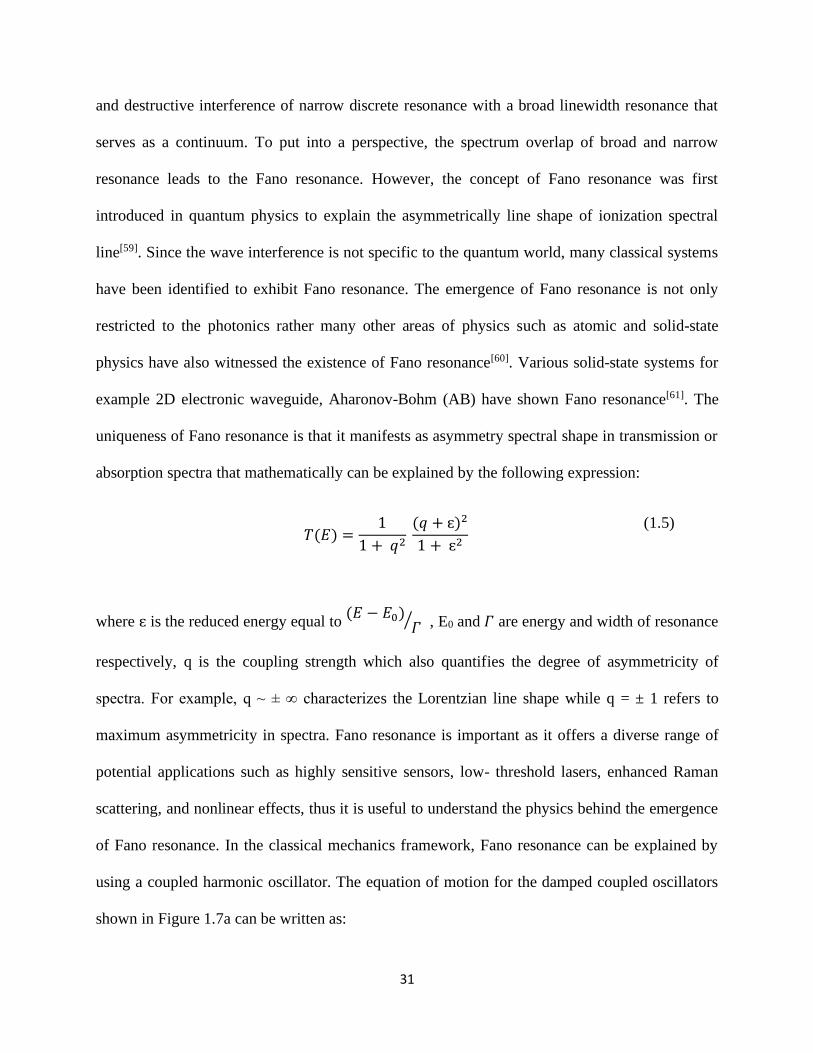
The amplitude of c1 and c2 are plotted in Figure 1.7 band d, where the position of resonance
corresponds to the real part of complex eigenmodes of equations 2 and 3. For frictionless second
oscillator i.e. 𝛾2 = 0 it is clear from Equation 4 that c1 = 0 at w = w2. This condition leads to the
sudden change in phase for the first oscillator at w= w2 as can be seen in Figure 1.7c. From the
phase plots of both the oscillators (Figure 1.7 c and e) it is clear that the first oscillator is out of
phase with the second oscillator at w = w2 which leads to the destructive interference. Here in
this system, the first oscillator can be consider as broad continuum as it is driven by continuous
external force while the second oscillator can be consider as discrete mode thus at the frequency
w = w2 the interference leads to the asymmetric spectra which is known as Fano resonance.
33
Figure 1.7 Classical picture of Fano resonance in coupled oscillator system (a) Artistic
sketch of the two coupled damped oscillators where one of them is driven by external force f1. (b
and d) Amplitude of the first and second coupled oscillator respectively (e and f) Phase acquired
by the first and second oscillators in the coupled system respectively[62].
In the context of MM structure, the emergence of Fano resonance in MM structure allows high-
density electric field confinement. This is useful for studying light-matter interactions for
example plasmon-phonon coupling and enhancing the nonlinear effect. In addition to this, the
high sensitivity of Fano resonance towards external perturbations make it an ideal candidate for
ultra-sensitive sensors.
For THz frequencies, the planar MM structures that support Fano resonance are vital for the
development of THz-based imaging, sensors, and communication systems. Many 2D materials
have spectral signature of phonon modes in THz region, thus the interaction of such 2D materials
with highly confined THz electric field would be interesting in unraveling the dynamics of
photon-phonon quasi particles.
In the scope of this thesis, we have taken the advantage of Fano resonance in planar THz
metamaterial to demonstrate ultrafast THz photonic devices. Fano resonance has been used as a
34
tool to quantify the ultrafast features of THz photonic devices. The unique asymmetric spectral
shape is the signature of Fano resonance. In MM there are multiple ways to achieve the Fano
resonance. Following the first demonstration of Fano resonance in the asymmetric split ring
arrays in microwave frequency[56], there have been many demonstrations based on breaking the
structural symmetry of split-ring resonator. The detailed discussion on the excitation of Fano
resonance in planar THz split-ring resonators is given in chapter 3.
1.7 Dynamic metamaterial in THz frequency
To add the active functionality in MM, the inclusion of dynamic materials with MM offers a
promising route. In this section, we present the potential of solution-processed perovskite as
dynamic material for ultrafast THz photonic devices.
1.7.1 Solution-processed semiconductor an effective route for ultrafast THz
devices
1.7.1a An overview of Halide perovskite vs conventional semiconductor
In modern days nanophotonics as well as optoelectronics and photovoltaics, the conventional
semiconductors like silicon (Si), gallium arsenide (GaAs) and germanium (Ge) have shown
remarkable performance. They have laid the foundation for many disruptive applications. In
recent years, a new family of semiconductors named as “halide perovskites” have emerged and
shown promising potentials for many applications ranging from optoelectronics, photovoltaics to
nanophotonics due to their unique electronic and optical properties (Figure 1.8). As compared to

35
conventional semiconductor perovskite shows inverted band structure[63] as shown in Figure 1.7.
That means in comparison to conventional semiconductors for example GaAs, the valence and
conduction band of perovskite shows opposite orbital characteristics. For example, the
conduction band of GaAs has s orbital character, whereas the valence band has p orbital
character. While on other hand, the valence band of perovskite has s orbital character whereas
the conduction band has p orbital character. This is because the valence band of perovskite is
mainly comprised with lead’s (Pb) s and X (i.e. halide) p anti bonding character whereas the
conduction band is composed of Pb p bands as shown in Figure. The advantage of having p
orbital character in the conduction band is having high density of states in the lower conduction
band owing to less dispersive nature of p orbital. Thus, halide perovskites have a stronger
interband transition dipole moment that yields a high absorption coefficient and high quantum
efficiency.
In addition to unique electronic band structure, the reversible bandgap tunability, supporting
stable excitons at room temperature, morphology engineering, and large scale ease of fabrication
at low cost, these are the added remarkable properties of perovskites that makes them important
and alternative promising options of materials for next-generation optoelectronics, photovoltaics,
nanophotonics, and ultrafast photonic devices. Below we briefly discuss the promising potential
of perovskite in various applications.
36
Figure 1.7 Band structure comparison of conventional semiconductor with halide
perovskite (a) Artistic sketch of the band structures of silicon (Si) and gallium arsenide (GaAs)
(b) Sketch of band structure of halide perovskite illustrating broadband and reverse tuning of
bandgap via changing anions. Dashed parabolic curve shows the existence of excitons in
perovskite at room temperature.
1.7.1b Photovoltaics:
In photovoltaic application silicon-based solar cells are well established at the commercial level
and used as sustainable energy sources. At wafer-scale both the polycrystalline and
monocrystalline silicon-based solar cells show remarkable ambience stability, heat resistivity and
good photoconversion efficiency. However, the major disadvantage of this silicon-based solar
device is poor absorbance owing to the indirect bandgap of silicon. To boost the absorption
requires an increase in active layer that increases the cost and puts a constraint in creating
flexible thin-film photovoltaic devices. On other hand, GaAs offer high absorption coefficient
due to their direct bandgap, better carrier lifetime and mobility, and low nonradiative energy
losses. But its high cost of production puts a major constraint for large-scale translation thus not
a feasible option at commercial scale.

37
In contrast, the halide perovskites offer optical properties close to GaAs i.e. high absorption
coefficient, and excellent electronic properties such as high electron mobility and
photoconversion efficiency (> 20 %)[64] that is favorable for thin-film photovoltaics application.
In addition to this, the major advantage offer by perovskite is its low production cost without
involving complex manufacturing processes. The wet chemistry and roll-to-roll techniques make
it possible to create cheap, flexible, and effective photovoltaics devices.
1.7.1c Lasers and LEDs:
Perovskites have shown excellent performance as light emitting devices (LEDs). Perovskite-
based LEDs have shown the efficiencies higher than 20%[64-66] owing to their direct bandgap,
strong excitons, high defect tolerance, and excellent color tunability features.
Also, the perovskite lasers based on microdisks, nanowires, and nano grating have shown low-
lasing thresholds, high defect stability, and spectral tunability[67]. In contrast, the pure silicon and
GaAs require additional doping or integration with quantum wells to perform as laser. However,
we should acknowledge that silicon and GaAs based sources widely used in telecom
wavelengths, where no compositions of halide perovskites are yet available.
1.7.1d Nonlinear optics:
In recent years there are many reports that shows the excellent nonlinear properties of halide
perovskites[68, 69]. Among the various perovskite family, the lead-free perovskites such as CsGeI3
and MAGeI3 have shown giant second harmonic generation with χ2 value exceeding 150 pm V-1,
which is comparable to GaAs and far better than silicon[70]. Also, third-harmonic generation with
third order susceptibilities χ3 exceeding 10-17 m2 V-2 has shown in perovskites[70, 71].
1.7.1e Integrated photonics:

38
Due to bandgap tunability and high refractive index, perovskite can be a potential option to
develop integrated photonics devices. The bandgap tunability offers unprecedented opportunities
for the reconfigurable photonic devices which is not possible with conventional semiconductors
like Si and GaAs. In addition, the ease of fabrication and process of perovskite-based nanowire,
nano-disks, nano grating, and metasurfaces offer a cheap and convenient route for futuristic nano
circuitry. However, we want to stress that the perovskite cannot overrule the existing developed
and advanced silicon-based platform for on-chip integrated photonics rather it offers an
additional alternative option for futuristic photonic devices owing to its excellent and tunable
optical properties.
1.9 Why Perovskite for THz applications?
In the quest for the development of ultrafast THz photonic devices, the active metamaterial is
vital. More particular, the dynamic material based active metamaterials have shown
unprecedented performance. For the candidate of dynamic materials, many semiconductor
options are available such silicon (Si), germanium (Ge) and gallium arsenide (GaAs). Among all
these conventional semiconductors each has their own advantage and disadvantages such as Si-
based active metamaterial can be CMOS compatible but require complex fabrication processes.
Ge based active metamaterials are ultrafast in nature but require high pump fluence to switch ON
and OFF the resonance[72]. Similarly, GaAs based active metadevice is good for ultrafast low
pump switching but requires complex fabrication process. In addition to these liquid crystals[73],
superconductor[8], graphene[74], VO2[75] and micro-electromechanical system (MEMS)[76] also
provides an effective route for realizing THz photonic devices.

39
On the other hand, halide perovskite presents itself as a potential candidate for ultrafast THz
photonic devices owing to its excellent electronic and optical properties and ease of fabrication
process and integration with metamaterials. This also allows to translate the perovskite based
active metamaterials to realize at flexible platform too that opens up a new avenue for flexible
THz photonic devices. Here we highlight a comparison between conventional semiconductors
and halide perovskite in Table.
Table 1: Comparison of different dynamic material based active THz metadevice.
Materials Speed Stimuli Modulation
amplitude
Integrated with
flexible platform
Silicon on sapphire
(SOS)[77]
~ ms 200 μJ/cm2 100 % No
GaAs (Gated)[51] ~ kHz 16 V 50 % No
GaAs
(photoexcitation)[50]
~ 1 ns 2 μJ/cm2 55 % No
VO2[75] 50 ms 40.5 K ~ 10 % No
Superconductor
(YBCO)[8]
~ ps 100 μJ/cm2 70 % No
MEMS[76] 30 kHz 16 V 56 % No
Ge[72] ~ ps ~ 1500 μJ/cm2 90 % Yes
Perovskite[78] ps-ns ~ 10 μJ/cm2 100 % Yes
1.10 Scope of the thesis
The area of photonics has seen rapid growth where significant efforts have been done in
understanding the fundamental as well as technological counterpart of electromagnetic waves. In
the electromagnetic spectrum, terahertz frequencies remained unnoticed till decades. However,
the vision of many disruptive applications such as high-speed wireless communication, high-
resolution imaging, sensing and spectroscopy has forced the researcher from both the world of

40
electronics as well as photonics to come together to elevate the field of terahertz research.
Metamaterial has played a significant role in fueling the terahertz research. It offers a simple and
efficient platform to potentially develop applications in the diverse field of technology such as
sensing, high volume data processing, wireless communication, and light-matter interactions.
This thesis aims to develop solution-processed semiconductor-based ultrafast terahertz photonic
devices. The control and manipulation of THz waves at ultrafast time scales is of great interest
for the basic as well as from technological aspects. Numerous interesting phenomena such as
altering the carrier dynamics due to strongly confined THz electric fields and quantum well
assisted excitonic effects at room temperature are effectively probed and discussed in the scope
of this thesis. The results presented in the thesis offer useful insight in light-matter interactions
and opens up an exciting and efficient way to develop THz photonic devices. The focus of the
thesis is not only to integrate dynamic material with metamaterials rather it also includes the
investigation of the effect of strongly confined THz electric field on the carrier dynamics of the
semiconductor. We for the first time unravel the dynamics of excitons in 2D perovskite using
time-resolved THz spectroscopy.
So far in this chapter, the overview and technical concepts of the MMs have been briefly
discussed. Further, a comprehensive comparison of solution-processed halide perovskite with
conventional semiconductors is also presented.
In chapter 2 we presented the detail of numerical tools that have been utilized to characterize the
optical properties of MM. Further, a detailed outlook of THz generation and detection for
photoconductive antenna and ZnTe crystal-based THz systems is presented. It also includes a

41
brief description of optical pump terahertz probe (OPTP) spectroscopy as it has been intensively
used in the latter part of the thesis.
Chapter 3 presents the ultrafast optical characterization of lead iodide (PbI2) followed by its
integration with terahertz Fano resonator metamaterial. This chapter discusses the all-optical
ultrafast switching of the THz electric field. Further, at the end of this chapter PbI2 thickness
dependent carrier dynamics are presented and showed that thickness indeed an important
parameter for dynamic materials-based active metadevices. And at the end, this chapter
concludes with altering the carrier dynamics of PbI2 thin film using the Purcell effect.
Chapter 4 includes the investigation of excitons as well as free carrier dynamics of 2D
perovskites using OPTP spectroscopy. For the first time using time-resolved THz spectroscopy,
we unravel the dynamics of excitons. Thanks to the quantum well structure of 2D perovskite that
enables the formation of stable exciton at room temperature as well as provides an additional
relaxation channel for the free electrons to relax back at ultrafast timescale. We leveraged the
ultrafast properties of 2D perovskite to develop ultrafast THz photonic devices by integrating 2D
perovskite with MM at rigid as well as a flexible platform.
The study presented in chapter 5 is important as it gives an insight on the carrier dynamics of
perovskite thin-film fabricated using various method. The results revealed that the choice of
solvent used in the fabrication of perovskite thin film is important as it affects the morphology as
result carrier dynamics. Thus, to utilize the perovskite thin film for various optoelectronic
applications these findings are vital.
42
Finally, in chapter 6, we presented the conclusion of each chapter and given a future outlook to
develop a multifunctional active THz device for next-generation applications like high-speed
wireless communication and THz interconnects.
1.11 References
[1] M. Tonouchi, Nature Photonics 2007, 1, 97.
[2] K. Ajito, Y. Ueno, IEEE Transactions on Terahertz Science and Technology 2011, 1, 293. [3] S. Koenig, D. Lopez-Diaz, J. Antes, F. Boes, R. Henneberger, A. Leuther, A. Tessmann, R.
Schmogrow, D. Hillerkuss, R. Palmer, T. Zwick, C. Koos, W. Freude, O. Ambacher, J. Leuthold, I.
Kallfass, Nature Photonics 2013, 7, 977.
[4] J. Federici, L. Moeller, Journal of Applied Physics 2010, 107, 111101. [5] W. S. Holland, J. S. Greaves, B. Zuckerman, R. A. Webb, C. McCarthy, I. M. Coulson, D. M.
Walther, W. R. F. Dent, W. K. Gear, I. Robson, Nature 1998, 392, 788.
[6] P. Han, X. Wang, Y. Zhang, Advanced Optical Materials 2020, 8, 1900533. [7] A. Tomadin, S. M. Hornett, H. I. Wang, E. M. Alexeev, A. Candini, C. Coletti, D. Turchinovich,
M. Kläui, M. Bonn, F. H. L. Koppens, E. Hendry, M. Polini, K.-J. Tielrooij, Science Advances 2018, 4,
eaar5313.
[8] Y. K. Srivastava, M. Manjappa, L. Cong, H. N. S. Krishnamoorthy, V. Savinov, P. Pitchappa, R. Singh, Advanced Materials 2018, 30, 1801257.
[9] B. Ferguson, X.-C. Zhang, Nature Materials 2002, 1, 26.
[10] T. Nagatsuma, G. Ducournau, C. C. Renaud, Nature Photonics 2016, 10, 371. [11] Y. Yuan, Y. Zhao, B. Zong, S. Parolari, Science China Information Sciences 2020, 63, 183301.
[12] I. F. Akyildiz, J. M. Jornet, C. Han, Physical Communication 2014, 12, 16.
[13] H. A. Gebbie, N. W. B. Stone, F. D. Findlay, Nature 1964, 202, 685. [14] D. H. Auston, A. M. Glass, P. LeFur, Applied Physics Letters 1973, 23, 47.
[15] D. H. Auston, K. P. Cheung, J. Opt. Soc. Am. B 1985, 2, 606.
[16] D. Grischkowsky, S. Keiding, M. van Exter, C. Fattinger, J. Opt. Soc. Am. B 1990, 7, 2006.
[17] M. Helm, E. Colas, P. England, F. DeRosa, S. J. A. Jr., Applied Physics Letters 1988, 53, 1714. [18] J. Faist, F. Capasso, D. L. Sivco, C. Sirtori, A. L. Hutchinson, A. Y. Cho, Science 1994, 264, 553.
[19] A. W. M. Lee, Q. Qin, S. Kumar, B. S. Williams, Q. Hu, J. L. Reno, Applied Physics Letters
2006, 89, 141125. [20] M. Franckié, D. O. Winge, J. Wolf, V. Liverini, E. Dupont, V. Trinité, J. Faist, A. Wacker, Opt.
Express 2015, 23, 5201.
[21] Y. Zeng, U. Chattopadhyay, B. Zhu, B. Qiang, J. Li, Y. Jin, L. Li, A. G. Davies, E. H. Linfield, B. Zhang, Y. Chong, Q. J. Wang, Nature 2020, 578, 246.
[22] Y. Ren, R. Wallis, D. S. Jessop, R. Degl'Innocenti, A. Klimont, H. E. Beere, D. A. Ritchie,
Applied Physics Letters 2015, 107, 011107.
[23] J. Darmo, V. Tamosiunas, G. Fasching, J. Kröll, K. Unterrainer, M. Beck, M. Giovannini, J. Faist, C. Kremser, P. Debbage, Opt. Express 2004, 12, 1879.
[24] Y. Chassagneux, J. Palomo, R. Colombelli, S. Dhillon, C. Sirtori, H. Beere, J. Alton, D. Ritchie,
Applied Physics Letters 2007, 90, 091113. [25] K. Lien Nguyen, M. L. Johns, L. F. Gladden, C. H. Worrall, P. Alexander, H. E. Beere, M.
Pepper, D. A. Ritchie, J. Alton, S. Barbieri, E. H. Linfield, Opt. Express 2006, 14, 2123.

43
[26] T. Nagatsuma, Y. Fujita, Y. Yasuda, Y. Kanai, S. Hisatake, M. Fujiwara, J. Kani, "Real-time 100-Gbit/s QPSK transmission using photonics-based 300-GHz-band wireless link", presented at 2016 IEEE
International Topical Meeting on Microwave Photonics (MWP), 31 Oct.-3 Nov. 2016, 2016.
[27] A. Hirata, T. Kosugi, H. Takahashi, R. Yamaguchi, F. Nakajima, T. Furuta, H. Ito, H. Sugahara,
Y. Sato, T. Nagatsuma, IEEE Transactions on Microwave Theory and Techniques 2006, 54, 1937. [28] A. Hirata, H. Takahashi, R. Yamaguchi, T. Kosugi, K. Murata, T. Nagatsuma, N. Kukutsu, Y.
Kado, J. Lightwave Technol. 2008, 26, 2338.
[29] N. Nishigami, Y. Nishida, S. Diebold, J. Kim, M. Fujita, T. Nagatsuma, "Resonant Tunneling Diode Receiver for Coherent Terahertz Wireless Communication", presented at 2018 Asia-Pacific
Microwave Conference (APMC), 6-9 Nov. 2018, 2018.
[30] S. Diebold, K. Tsuruda, M. Fujita, T. Nagatsuma, J. Kim, T. Mukai, "Terahertz resonant tunneling diode systems for next generation wireless communication", presented at 2015 IEEE
International Meeting for Future of Electron Devices, Kansai (IMFEDK), 4-5 June 2015, 2015.
[31] S. Dasgupta, Notes and Records of the Royal Society of London 1998, 52, 307.
[32] I. V. Lindell, A. H. Sihvola, J. Kurkijarvi, IEEE Antennas and Propagation Magazine 1992, 34, 24.
[33] V. G. Veselago, Soviet Physics Uspekhi 1968, 10, 509.
[34] J. B. Pendry, A. J. Holden, W. J. Stewart, I. Youngs, Physical Review Letters 1996, 76, 4773. [35] D. R. Smith, D. C. Vier, W. Padilla, S. C. Nemat-Nasser, S. Schultz, Applied Physics Letters
1999, 75, 1425.
[36] D. R. Smith, W. J. Padilla, D. C. Vier, S. C. Nemat-Nasser, S. Schultz, Physical Review Letters 2000, 84, 4184.
[37] D. R. Smith, J. B. Pendry, M. C. K. Wiltshire, Science 2004, 305, 788.
[38] J. Pendry, Nature 2009, 460, 579.
[39] J. Pendry, Nature Materials 2006, 5, 599. [40] W. J. Padilla, D. N. Basov, D. R. Smith, Materials Today 2006, 9, 28.
[41] K. Aydin, I. Bulu, E. Ozbay, Opt. Express 2005, 13, 8753.
[42] N. Fang, H. Lee, C. Sun, X. Zhang, Science 2005, 308, 534. [43] X. Zhang, Z. Liu, Nature Materials 2008, 7, 435.
[44] J. B. Pendry, D. Schurig, D. R. Smith, Science 2006, 312, 1780.
[45] D. Schurig, J. J. Mock, B. J. Justice, S. A. Cummer, J. B. Pendry, A. F. Starr, D. R. Smith,
Science 2006, 314, 977. [46] N. I. Landy, S. Sajuyigbe, J. J. Mock, D. R. Smith, W. J. Padilla, Physical Review Letters 2008,
100, 207402.
[47] H. Tao, N. I. Landy, C. M. Bingham, X. Zhang, R. D. Averitt, W. J. Padilla, Opt. Express 2008, 16, 7181.
[48] X. Q. Lin, T. J. Cui, J. Y. Chin, X. M. Yang, Q. Cheng, R. Liu, Applied Physics Letters 2008, 92,
131904. [49] Q. Cheng, H. F. Ma, T. J. Cui, Applied Physics Letters 2009, 95, 181901.
[50] W. J. Padilla, A. J. Taylor, C. Highstrete, M. Lee, R. D. Averitt, Physical Review Letters 2006,
96, 107401.
[51] H.-T. Chen, W. J. Padilla, J. M. O. Zide, A. C. Gossard, A. J. Taylor, R. D. Averitt, Nature 2006, 444, 597.
[52] P. Pitchappa, M. Manjappa, C. P. Ho, R. Singh, N. Singh, C. Lee, Advanced Optical Materials
2016, 4, 541. [53] R. Liu, T. J. Cui, D. Huang, B. Zhao, D. R. Smith, Physical Review E 2007, 76, 026606.
[54] D. R. Smith, J. B. Pendry, J. Opt. Soc. Am. B 2006, 23, 391.
[55] J. B. Pendry, A. J. Holden, D. J. Robbins, W. J. Stewart, IEEE Transactions on Microwave Theory and Techniques 1999, 47, 2075.
[56] V. A. Fedotov, M. Rose, S. L. Prosvirnin, N. Papasimakis, N. I. Zheludev, Physical Review
Letters 2007, 99, 147401.
44
[57] N. Papasimakis, V. A. Fedotov, N. I. Zheludev, S. L. Prosvirnin, Physical Review Letters 2008, 101, 253903.
[58] C. Wu, A. B. Khanikaev, G. Shvets, Physical Review Letters 2011, 106, 107403.
[59] U. Fano, Physical Review 1961, 124, 1866.
[60] A. B. Khanikaev, C. Wu, G. Shvets, Nanophotonics 2013, 2, 247. [61] A. R. P. Rau, Physica Scripta 2004, 69, C10.
[62] Y. S. Joe, A. M. Satanin, C. S. Kim, Physica Scripta 2006, 74, 259.
[63] A. S. Berestennikov, P. M. Voroshilov, S. V. Makarov, Y. S. Kivshar, Applied Physics Reviews 2019, 6, 031307.
[64] A. Fakharuddin, F. D. Rossi, T. M. Watson, L. Schmidt-Mende, R. Jose, APL Materials 2016, 4,
091505. [65] K. Lin, J. Xing, L. N. Quan, F. P. G. de Arquer, X. Gong, J. Lu, L. Xie, W. Zhao, D. Zhang, C.
Yan, W. Li, X. Liu, Y. Lu, J. Kirman, E. H. Sargent, Q. Xiong, Z. Wei, Nature 2018, 562, 245.
[66] W. Xu, Q. Hu, S. Bai, C. Bao, Y. Miao, Z. Yuan, T. Borzda, A. J. Barker, E. Tyukalova, Z. Hu,
M. Kawecki, H. Wang, Z. Yan, X. Liu, X. Shi, K. Uvdal, M. Fahlman, W. Zhang, M. Duchamp, J.-M. Liu, A. Petrozza, J. Wang, L.-M. Liu, W. Huang, F. Gao, Nature Photonics 2019, 13, 418.
[67] Q. Wei, X. Li, C. Liang, Z. Zhang, J. Guo, G. Hong, G. Xing, W. Huang, Advanced Optical
Materials 2019, 7, 1900080. [68] A. Ferrando, J. P. Martínez Pastor, I. Suárez, The Journal of Physical Chemistry Letters 2018, 9,
5612.
[69] J. Xu, X. Li, J. Xiong, C. Yuan, S. Semin, T. Rasing, X.-H. Bu, Advanced Materials 2020, 32, 1806736.
[70] I. Abdelwahab, G. Grinblat, K. Leng, Y. Li, X. Chi, A. Rusydi, S. A. Maier, K. P. Loh, ACS
Nano 2018, 12, 644.
[71] S. V. Makarov, M. I. Petrov, U. Zywietz, V. Milichko, D. Zuev, N. Lopanitsyna, A. Kuksin, I. Mukhin, G. Zograf, E. Ubyivovk, D. A. Smirnova, S. Starikov, B. N. Chichkov, Y. S. Kivshar, Nano
Letters 2017, 17, 3047.
[72] W. X. Lim, M. Manjappa, Y. K. Srivastava, L. Cong, A. Kumar, K. F. MacDonald, R. Singh, Advanced Materials 2018, 30, 1705331.
[73] S. Savo, D. Shrekenhamer, W. J. Padilla, Advanced Optical Materials 2014, 2, 275.
[74] S. H. Lee, M. Choi, T.-T. Kim, S. Lee, M. Liu, X. Yin, H. K. Choi, S. S. Lee, C.-G. Choi, S.-Y.
Choi, X. Zhang, B. Min, Nature Materials 2012, 11, 936. [75] T. Driscoll, H.-T. Kim, B.-G. Chae, B.-J. Kim, Y.-W. Lee, N. M. Jokerst, S. Palit, D. R. Smith,
M. Di Ventra, D. N. Basov, Science 2009, 325, 1518.
[76] X. Liu, W. J. Padilla, Advanced Optical Materials 2013, 1, 559. [77] J. Gu, R. Singh, X. Liu, X. Zhang, Y. Ma, S. Zhang, S. A. Maier, Z. Tian, A. K. Azad, H.-T.
Chen, A. J. Taylor, J. Han, W. Zhang, Nature Communications 2012, 3, 1151.
[78] M. Manjappa, Y. K. Srivastava, A. Solanki, A. Kumar, T. C. Sum, R. Singh, Advanced Materials
2017, 29, 1605881.

45
46
Chapter 2
Simulation, Characterization technique and
Fabrication
This chapter overviews the basics of the numerical tool that has been extensively used to
simulate the electromagnetic response of the metamaterial (MM). Section 2.1 describes the steps
involved in modeling the metasurface using CST Microwave studio. To characterize the
metamaterial resonance spectra, we used the latest version of CST 2019. Section 2.2 discusses
the theoretical details of terahertz time domain spectroscopy (THz-TDS). The detailed discussion
on Photoconductive antenna (PCA) and ZnTe crystal-based THz-TDS are given in sections 2.2a
and 2.2b respectively. Section 2.3 sketches the theoretical and experimental outline of an optical
pump and terahertz probe (OPTP), which is the heart of this thesis. Section 2.4 discusses the
fabrication procedure, which is utilized for fabricating the metamaterial (MM) structures.
2.1 Electromagnetic Simulation of terahertz metamaterial
This section describes the principle and techniques involved in numerical simulation to
characterize the electromagnetic response of metamaterial (MM) resonators. Numerical
simulation provides an ideal platform to design, optimize and analyze the electromagnetic
response of metamaterial structures. We used a commercially available software named
Computer Simulation Technology Microwave studio (CST-MWS). It solves the integral form of
Maxwell’s equation using Finite Integral Technique (FIT) and Finite element method (FEM)

47
based on the selected solver. The Maxwell’s equation in integral form in a medium of volume
“V” containing charge density “ρ” and current density “𝐽” can be written as:
∮𝑫.⃗⃗ ⃗⃗𝑆
𝑑𝑆⃗⃗ ⃗⃗⃗ = ∫ ρ𝐝𝐕 𝑉
∮𝑩.⃗⃗ ⃗⃗𝑆
𝑑𝑆⃗⃗ ⃗⃗⃗ = 0
∮ 𝑬.⃗⃗⃗⃗⃗𝑙
𝑑𝑙⃗⃗⃗⃗ = ∫ (−∂�⃗⃗�
∂t. 𝑑𝑆⃗⃗ ⃗⃗⃗)
𝑆
∮𝑯.⃗⃗⃗⃗⃗𝑙
𝑑𝑙⃗⃗⃗⃗
(2.1)
where, �⃗⃗⃗�, �⃗⃗⃗�, �⃗⃗⃗� and �⃗⃗⃗⃗� are the displacement current, electric field, magnetic field and
magnetizing field, respectively.
One of the significant added advantages of using CST-MWS is its enrich CAD environment that
allows designing the MM structure in a simple way. In addition to this, CST-MWS contains a
wide range of materials library which includes frequency-dependent complex permittivity of
many commonly used materials like silicon, quartz etc. It also provides the freedom to define a
broad range of user-defined materials with frequency-dependent dispersion. The predefined
model such as Drude and Lorentz can also be used by defining the appropriate parameters
require like scattering rate, plasma frequency etc.
CST offers mainly two types of solvers to characterize the MM structures: these are frequency
domain solver and time domain solver. Although, both give similar output results but the
implementation of both is specific to the problems. The frequency-domain solver is more
appropriate for the structures with the resonant response, while on the other hand, time domain
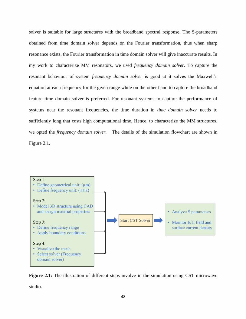
48
solver is suitable for large structures with the broadband spectral response. The S-parameters
obtained from time domain solver depends on the Fourier transformation, thus when sharp
resonance exists, the Fourier transformation in time domain solver will give inaccurate results. In
my work to characterize MM resonators, we used frequency domain solver. To capture the
resonant behaviour of system frequency domain solver is good at it solves the Maxwell’s
equation at each frequency for the given range while on the other hand to capture the broadband
feature time domain solver is preferred. For resonant systems to capture the performance of
systems near the resonant frequencies, the time duration in time domain solver needs to
sufficiently long that costs high computational time. Hence, to characterize the MM structures,
we opted the frequency domain solver. The details of the simulation flowchart are shown in
Figure 2.1.
Figure 2.1: The illustration of different steps involve in the simulation using CST microwave
studio.
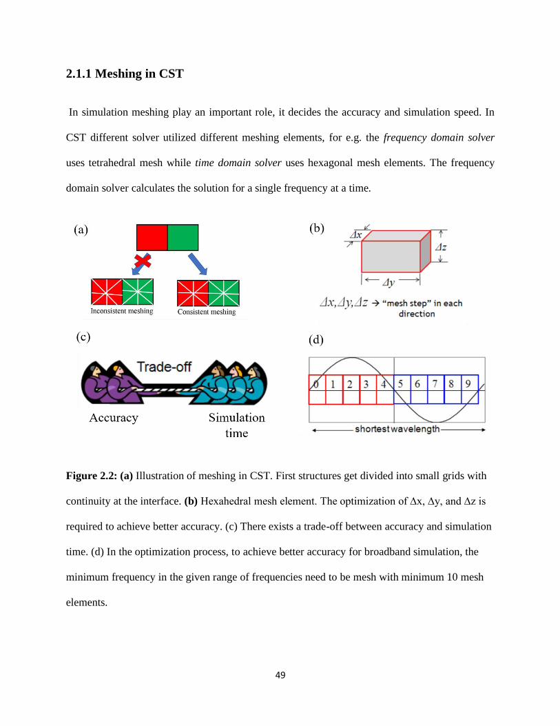
49
2.1.1 Meshing in CST
In simulation meshing play an important role, it decides the accuracy and simulation speed. In
CST different solver utilized different meshing elements, for e.g. the frequency domain solver
uses tetrahedral mesh while time domain solver uses hexagonal mesh elements. The frequency
domain solver calculates the solution for a single frequency at a time.
Figure 2.2: (a) Illustration of meshing in CST. First structures get divided into small grids with
continuity at the interface. (b) Hexahedral mesh element. The optimization of ∆x, ∆y, and ∆z is
required to achieve better accuracy. (c) There exists a trade-off between accuracy and simulation
time. (d) In the optimization process, to achieve better accuracy for broadband simulation, the
minimum frequency in the given range of frequencies need to be mesh with minimum 10 mesh
elements.

50
For each frequency sample, the linear equation system is solved either by iterative solver or
sparse direct solver. The solution for each frequency consists of S-parameters, field distribution
and derived parameters. In order to get the accurate results, the solver requires consistent
meshing specially at the interface of the different medium as shown in Figure 2.2 in red and
green color.
How meshing works: - To solve the Maxwell’s equation numerically the entire geometry is
divided into a small volume and to do so different solver uses different types of mesh element
which is called “mesh cell”. For example, time domain solver uses hexahedral mesh where the
computational volume is discretized by using variable sized rectangular cuboids as shown in
Figure 2.2b. While frequency domain solver utilizes tetrahedral mesh elements. In both the cases
the in discretized form each mesh elements represents the small volume where electric and
magnetic field are computed. Thus, more the number of mesh elements the more accurately field
gradient will be captured but at the cost of high computational time. There exists a trade off
between accuracy and computational time (Figure 2.2c). To optimize this the time step at which
signal propagates into the computational domains need to be optimized. The time step of the
signal depends on mesh element size according to Courant stability condition as:
𝛥𝑡𝑚𝑎𝑥 <
1
𝑢𝑚𝑎𝑥 [1
𝛥𝑋2+
1
𝛥𝑌2+
1
𝛥𝑍2]−1/2
(2.2)
where, 𝑢𝑚𝑎𝑥 is the maximum phase velocity and ΔX, ΔY and ΔZ are the change in length of
mesh cell in x, y and z-direction respectively. From Equation 2.2 it is clear that to maximize the
time step the smallest mesh cell need to be large. While on the other hand, the largest mesh cell
size is also an important parameter. The mesh size cannot be arbitrarily large as it will induce
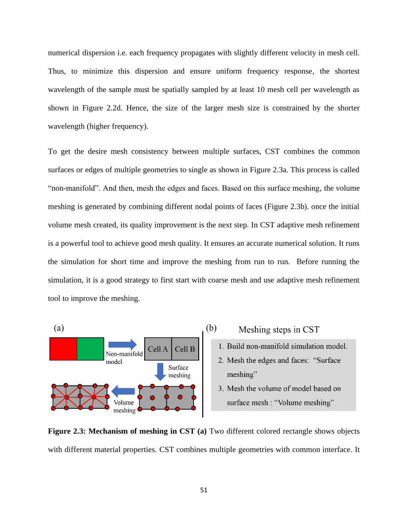
51
numerical dispersion i.e. each frequency propagates with slightly different velocity in mesh cell.
Thus, to minimize this dispersion and ensure uniform frequency response, the shortest
wavelength of the sample must be spatially sampled by at least 10 mesh cell per wavelength as
shown in Figure 2.2d. Hence, the size of the larger mesh size is constrained by the shorter
wavelength (higher frequency).
To get the desire mesh consistency between multiple surfaces, CST combines the common
surfaces or edges of multiple geometries to single as shown in Figure 2.3a. This process is called
“non-manifold”. And then, mesh the edges and faces. Based on this surface meshing, the volume
meshing is generated by combining different nodal points of faces (Figure 2.3b). once the initial
volume mesh created, its quality improvement is the next step. In CST adaptive mesh refinement
is a powerful tool to achieve good mesh quality. It ensures an accurate numerical solution. It runs
the simulation for short time and improve the meshing from run to run. Before running the
simulation, it is a good strategy to first start with coarse mesh and use adaptive mesh refinement
tool to improve the meshing.
Figure 2.3: Mechanism of meshing in CST (a) Two different colored rectangle shows objects
with different material properties. CST combines multiple geometries with common interface. It

52
is called non-manifold. In the next step the meshing of common edges or surfaces occur followed
by volume meshing. (b) Illustrates the steps involve in the meshing as shown in (a).
After the adequate quality of meshing, CST shows the meshed structure in mesh view option.
Here, to avoid the simulation artifact the we keep the number of cells per wavelength 10 as
shown in Figure 2.4.
Figure 2.4: Schematic after mesh adaptation using tetrahedral mesh grids in frequency domain
solver. The metallic part of the resonators is shown in yellow color and the thick substrate is
shown in blue. For better accuracy of the simulation results we select 10 mesh cells per
wavelength.
2.1.2 Boundary conditions
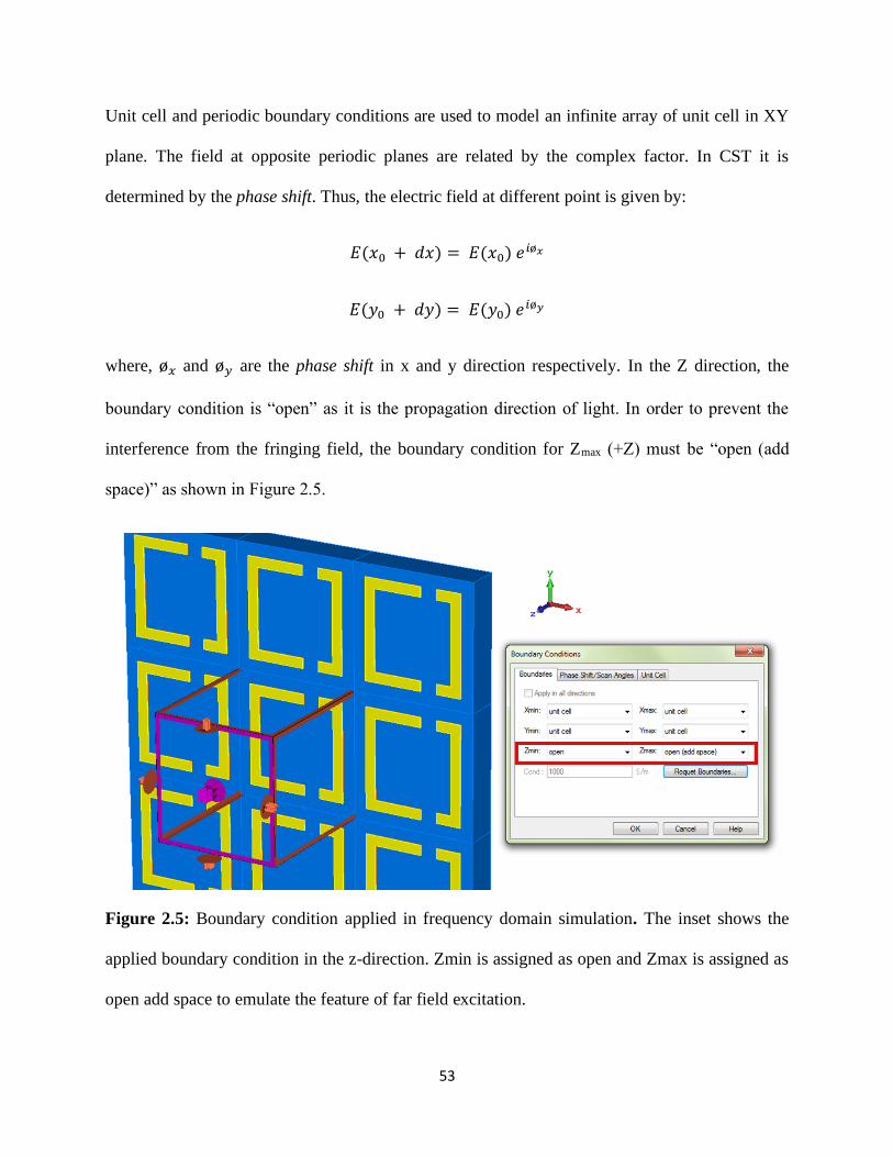
53
Unit cell and periodic boundary conditions are used to model an infinite array of unit cell in XY
plane. The field at opposite periodic planes are related by the complex factor. In CST it is
determined by the phase shift. Thus, the electric field at different point is given by:
𝐸(𝑥0 + 𝑑𝑥) = 𝐸(𝑥0) 𝑒𝑖ø𝑥
𝐸(𝑦0 + 𝑑𝑦) = 𝐸(𝑦0) 𝑒𝑖ø𝑦
where, ø𝑥 and ø𝑦 are the phase shift in x and y direction respectively. In the Z direction, the
boundary condition is “open” as it is the propagation direction of light. In order to prevent the
interference from the fringing field, the boundary condition for Zmax (+Z) must be “open (add
space)” as shown in Figure 2.5.
Figure 2.5: Boundary condition applied in frequency domain simulation. The inset shows the
applied boundary condition in the z-direction. Zmin is assigned as open and Zmax is assigned as
open add space to emulate the feature of far field excitation.

54
2.1.3 Interpretation of simulated data
After the simulation, the transmission and reflection spectra are calculated using S-parameters,
that relates the input and output waves via scattering matrix (as shown in Figure 2.6).
Mathematically for two ports system it can be written as:
(𝑏1𝑏2) = (
𝑆11 𝑆12𝑆21 𝑆22
) (𝑎1𝑎2)
(2.4)
where, ai represents the incident wave to port i and bj represents the reflected wave from port j.
The elements in S-matrix Spq are complex in nature which contains both the information of
amplitude and phase. Here subscript “q” represents the excitation port (i.e. input port) while “p”
represents the output port. Thus, S11 represents the ratio of the amplitude of wave reflects from
port 1 to the amplitude of signal incident on port 1. Mathematically, all the elements of S-matrix
can be calculated using:
𝑆11 =𝑏1𝑎1⁄ ; 𝑆12 =
𝑏1𝑎2⁄
𝑆21 =𝑏2𝑎1⁄ ; 𝑆22 =
𝑏2𝑎2⁄
(2.5)
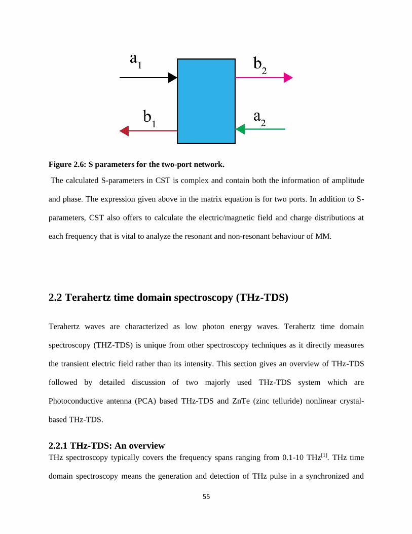
55
Figure 2.6: S parameters for the two-port network.
The calculated S-parameters in CST is complex and contain both the information of amplitude
and phase. The expression given above in the matrix equation is for two ports. In addition to S-
parameters, CST also offers to calculate the electric/magnetic field and charge distributions at
each frequency that is vital to analyze the resonant and non-resonant behaviour of MM.
2.2 Terahertz time domain spectroscopy (THz-TDS)
Terahertz waves are characterized as low photon energy waves. Terahertz time domain
spectroscopy (THZ-TDS) is unique from other spectroscopy techniques as it directly measures
the transient electric field rather than its intensity. This section gives an overview of THz-TDS
followed by detailed discussion of two majorly used THz-TDS system which are
Photoconductive antenna (PCA) based THz-TDS and ZnTe (zinc telluride) nonlinear crystal-
based THz-TDS.
2.2.1 THz-TDS: An overview
THz spectroscopy typically covers the frequency spans ranging from 0.1-10 THz[1]. THz time
domain spectroscopy means the generation and detection of THz pulse in a synchronized and

56
coherent manner[2]. In other words, THZ-TDS is an efficient technique for generation and
detection of broadband coherent THz radiation. Other spectroscopy techniques such as vector
network analyzers or IR-Vis-UV spectroscopy performs frequency domain measurement via
frequency sweeping. While Fourier-transformed infrared spectrometers (FTIR) indirectly
measure the time domain via interferometry[3].
In contrast, THz TDS offers direct access to the amplitude and phase of the THz electric field
that makes it unique. It allows to capture many useful information such as complex optical
constants of material without using Kramer-Kronig transformation relation. In the context of
material characterization, it is extremely useful, as the free carriers either reflect or absorb the
THz radiation. THz-TDS has been intensively utilized for the characterization of topological
insulators (TI)[4, 5], superconductors[6, 7], phase change materials[8] and 2D materials[9, 10]. In
addition to this, THz-TDS has broad prospect for various real-life applications such as virus
detection[11], food-quality inspection[1] and security scanning[12].
An ultrafast femtosecond laser with a pulse width ranging from 100-10 fs plays a crucial role in
THz-TDS as it utilizes for both the generation and detection of THz waves. Section 2.2.2 and
2.2.3 present the detailed discussion of PCA and ZnTe based THz-TDS, respectively. Since the
THz electric field has a time duration of few picoseconds, thus it requires a fast and sensitive
detection technique. The electronic circuit-based detector lacks such fast sensitivity and high
time resolution. Thus, it requires a special detection technique. One of the ways to reach sub-
picosecond resolution is by using an optical technique where an ultrafast laser pulse can be used
to generate and detect the transient THz field.

57
Concept behind detecting the THz pulse: Capturing the time-domain spectra of THz field can
be seen as sampling unknown THz field with a known femtosecond laser pulse. The
femtosecond laser pulse that samples the THz electric field is known as “read-out pulse”.
Usually, in the THz-TDS, the convolution of short readout pulse and long THz pulse is being
detected. To perform coherent detection, the optical read out and THz pulse must arrive
simultaneously. Figure 2.7.a shows the schematic of the experimental setup to capture the full-
time domain THz pulse. The femtosecond laser pulse split into two parts by beam splitter. One
part being used for THz generation thus send to the emitter and other part used for coherent
detection of THz wave. To achieve the time delay between optical and THz pulse, a mechanical
delay stage is used with micrometer precision thus picosecond resolution in time domain. The
different colors marked in Figure 2.7.a represents the various time instance of the delay stage,
and the corresponding amplitude of THz electric field is shown in Figure 2.7.b. Thus, by moving
the delay stage with smaller steps full THz time domain electric pulse mapped out.
Here two important points to be noted:
a. Femtosecond laser and THz pulse must arrive simultaneously.
b. The width of optical pulse must be significantly shorter than THz pulse.
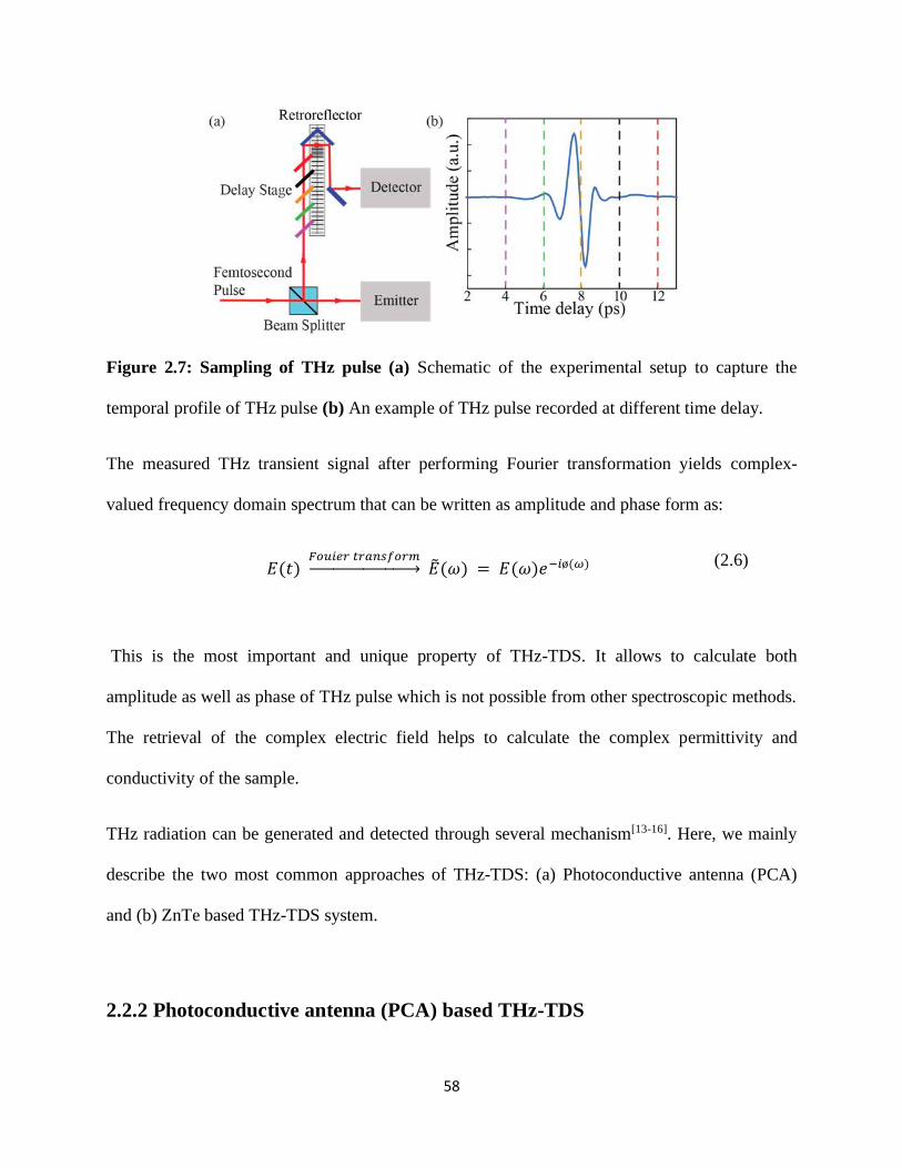
58
Figure 2.7: Sampling of THz pulse (a) Schematic of the experimental setup to capture the
temporal profile of THz pulse (b) An example of THz pulse recorded at different time delay.
The measured THz transient signal after performing Fourier transformation yields complex-
valued frequency domain spectrum that can be written as amplitude and phase form as:
𝐸(𝑡) 𝐹𝑜𝑢𝑖𝑒𝑟 𝑡𝑟𝑎𝑛𝑠𝑓𝑜𝑟𝑚→ �̃�(𝜔) = 𝐸(𝜔)𝑒−𝑖ø(𝜔) (2.6)
This is the most important and unique property of THz-TDS. It allows to calculate both
amplitude as well as phase of THz pulse which is not possible from other spectroscopic methods.
The retrieval of the complex electric field helps to calculate the complex permittivity and
conductivity of the sample.
THz radiation can be generated and detected through several mechanism[13-16]. Here, we mainly
describe the two most common approaches of THz-TDS: (a) Photoconductive antenna (PCA)
and (b) ZnTe based THz-TDS system.
2.2.2 Photoconductive antenna (PCA) based THz-TDS

59
PCA based THz-TDS is one of the most widely used THz spectroscopy systems with high
signal-to-noise ratio (~ 10000:1)[17, 18]. The generation and detection of THz is based on
photocarrier transport process. An antenna is used to generate and detect the THz waves. The
commonly used antenna architect contains parallel metallic microstrip lines fabricated on
photoconductive substrate (low-temperature GaAs). The schematic of PCA-based THz-TDS is
shown in Figure 2.9.
2.2.2a THz generation from PCA
An ultrafast optical pulse with a high repetition rate ((1 kHz)) is used for the generation and
detection of THz pulse. Figure 2.8 shows the schematic of PCA based THz spectroscopy setup.
The optical laser pulse (in Figure 2.8 Femtosecond laser pulse, 800 nm) is divided into two parts
using beam splitter. One part of beam is directed to the emitter antenna while the second beam is
utilized for THz detection. The emitter PCA consists of two metallic electrodes on low
semiconducting substrate as shown by dashed circles in Figure 2.8. In our setup the PCA antenna
was fabricated on GaAs substrate owing to high electronic mobility and ultrafast photocarrier
relaxation[19]. One part of the femtosecond pulse incident on the antenna with photon energy
higher than the bandgap of the semiconductor substrate (Eg for GaAs 1.424eV[20] and E800nm ~
1.51 eV) results in generating a transient photocurrent. Upon laser illumination, there exists a
rapid rise in transient current followed by a longer decay due to finite carrier lifetime. These
transient photocurrents induces the time-varying surface currents (J(t)) which are accelerated by
applying DC voltage across the electrodes of antenna which in turn emits THz radiation[21-23].
Mathematically, the photogenerated current density (J(t)) can be written as:
𝐽(𝑡) = 𝑁(𝑡) 𝑒 µ 𝐸𝑏 (2.7)
60
where, Eb is the electric field produced by biasing electrodes with DC voltage, N(t) is the
photoinduced free carrier density, e is the electronic charge and µ is the mobility of electrons. To
achieve large current density (J(t)), high electronic mobility is favorable. In Eqn.2.7, we neglect
the contribution of holes owing to is low mobility as compared to electrons. The strength of
radiated THz electric field is given by i.e. ETHz[24]:
𝐸𝑇𝐻𝑧 =
𝐴𝑒
4𝜋ɛ0𝑐2𝑧 𝜕𝑁(𝑡)
𝜕𝑡 µ 𝐸𝑏
(2.8)
where, A is the optically illuminated area in the semiconductor substrate located between the
electrodes, ɛ0 is the vacuum permittivity, c is the speed of light and z is the distance between the
emitter and far-field probe. To achieve high bandwidth, the lifetime of free carriers must be short
(in the range of picoseconds), thus substrate with ultrafast free carrier dynamics are always
preferable. Low temperature gallium arsenide (LT-GaAs) is one of the commonly used
substrates for PCA emitter. Also, the strength of THz electric field is directly proportional to the
electron mobility of the substrate. Thus, high mobility substrates are an ideal choice for
fabricating PCA emitter. In this regard, LT-GaAs substrate is perfect candidate owing to high
electronic mobility (~ 8500 cm2V-1s-1 [20]) and ultrafast carrier relaxation (~ few picoseconds[19]).
The polarization of emitted THz radiation is along the biased field direction. This information is
vital to detect the THz radiation using PCA (described in section 2.2.2b). One important point
must be noted here that, significant part of the energy of THz radiation is emitted during the rise
of photocurrent and most of the energy is coupled to the substrate rather than air, this the reason
why a hemispherical silicon lens is attached to the substrate opposite to the dipole antenna as
shown in left dashed circle in Figure 2.8.

61
Figure 2.7: Schematic of Photoconductive antenna-based THz-TDS. The inset shows the
zoomed part of THz emitter and detector section.
2.2.2b THz detection using PCA
The detection process using PCA is the reverse of the generation process. At the detector side,
the second optical pulse generates free carriers which recombine in the absence of incidence THz
pulse. Once the THz pulse focused in the active region of PCA with polarization parallel to the
dipole, THz electric field acts as bias and sweep the free carriers across the photoconductive gap
and generates photocurrent (J) across the electrodes which is given as:
𝐽 = 𝑁 𝑒 µ 𝐸(𝜏) (2.9)

62
where N is the photocarrier density µ is electronic mobility, and 𝜏 is the temporal delay between
the optical probe and THz pulse. Since the lifetime of free carrier is much shorter than the THz
pulse duration, thus the magnitude of generated photocurrent represents the amplitude of THz
electric field at an instant. This process is called photoconductive sampling. At last, by varying
the time delay between THz and optical laser pulse, the entire waveform of THz pulse can be
recorded. In this process, the amplitude of generated photocurrent is very low typically on the
order of nanoampere thus current amplifier is used to amplify the photocurrent. To probe the full
waveform of THz electric field in time domain, 𝜏 is varied using mechanic delay stage as shown
in Figure 2.8.
2.2.3 ZnTe based THz-TDS
This is also one of the most intensively used THz-TDS system. As compared to PCA based THz-
TDS, the output of THz pulse is high in nonlinear crystal-based THz-TDS, which is vital for
many nonlinear spectroscopic applications. Nonlinear crystal is the key component for the
generation and detection of THz waves via a nonlinear optical process. In general, nonlinear
crystals uses amplifier laser system with high pulse energy for generating the THz waves. Thus,
it can also be utilized to develop a robust optical-pump terahertz probe (OPTP) spectroscopic
systems which is described in section 2.3.
A suitable nonlinear crystal should have a high transparency in both the optical and THz regime
to avoid the energy dissipation. In addition to this, to facilitate the high conversion efficiency, its
electrooptic coefficient must be sufficiently large. A number of materials satisfy these
requirements, that includes dielectric crystals e.g. LiNbO3, LiTaO3, semiconductors e.g. ZnTe,
GaAs, spintronics based emitter e.g. FeNi. In our studies, we employ ZnTe crystal-based THz-
63
TDS which further served as OPTP setup as well. A major factor that degrades the performance
of nonlinear crystal is the optical phonon absorption which typically falls in the THz region and
restrict the bandwidth of the THz generation. For example, ZnTe has optical phonon mode at 5.3
THz.
2.2.3a Generation process
The generation of THz from ZnTe crystal involves a nonlinear process which is known as optical
rectification. In this process, high intense optical beam induces a polarization in a nonlinear
medium. The most commonly used nonlinear crystal is ZnTe. It is noncentrosymmetric crystal
that has large 2nd order nonlinear susceptibility (χ2 = 1.6 × 10⁻⁷ m/V) and high electro-optic
coefficient r41 = 4.04 pm/V[25]. There are many parameters such as thickness, the orientation of
crystal, wavelength and intensity of incident beam that affects the efficiency of THz generation
from the ZnTe crystal. In the generation process, an ultrafast optical pulse (35 fs in our case)
interacts with the crystal that induces the transient polarization with the low frequency that
radiates transient electromagnetic field, whose frequencies span the THz region.
The optical rectification process requires second-order frequency mixing. Given that E(t) is the
electric field of the incident optical pulse, thus the second-order polarization induced inside a
nonlinear crystal is given by:
𝑃2(𝑡) 𝛼 𝜒2 𝐸(𝑡)2 (2.10)
where, χ is the second-order susceptibility of ZnTe crystal. Since the femtosecond optical pulse
contains many frequencies, by assuming only the two frequency components i.e.

64
𝑃2(𝑡) 𝛼 𝜒2[𝐸12𝑒−2𝑖𝜔1𝑡 + 𝐸2
2𝑒−2𝑖𝜔2𝑡 + 2𝐸1𝐸2𝑒−2𝑖(𝜔1+𝜔2)𝑡
+ 2𝐸1𝐸2∗𝑒−2𝑖(𝜔1−𝜔2)𝑡 + 𝑐. 𝑐. ]
+ 2𝜒2[𝐸1𝐸1∗ + 𝐸2𝐸2
∗]
(2.11)
here c.c. represents the complex conjugate. The polarization expression contains second
harmonics of E1, E2, sum-frequency and difference frequency. In optical rectification only the
difference frequency component i.e. E (ω1 – ω2) will be useful. Mathematically, the far-field
radiated THz electric field is related to the second-order derivative of second-order polarization:
𝐸𝑇𝐻𝑧(𝑡) 𝛼
𝛿2𝑃2(𝑡)
𝛿𝑡2
(2.12)
2.2.3b Detection process
The ZnTe based THz-TDS utilizes linear electro-optic (EO) effect or Pockels effect to resolve
the amplitude of subpicosecond transient THz electric field. It is the reverse of the optical
rectification process. This effect is related to the local change in optical birefringence (i.e.
different refractive index for light polarized in different axes of the crystal) of a crystal-induced
by the THz electric field. The change in birefringence induces the polarization change in low
intense optical probe pulse as shown in Figure 2.10. Modulating the probe laser pulse inside the
EO crystal is the basics behind the THz detection in EO sampling.

65
Figure 2.9: Schematic of free space electro-optic detection using ZnTe crystal.
In the presence of THz electric field, the co-propagated optical probe pulse experiences phase
delay due to induced birefringence that results in polarization change of probe pulse after passing
through the crystal. Generally, the optical probe pulse with linear polarization is incident to the
ZnTe crystal. That acquires modification in polarization due to birefringence of crystal and
become elliptically polarized. This change in polarization is recorded via polarization-sensitive
balanced detection. Figure 2.9 shows the schematic of THz detection using ZnTe crystal. In the
absence of THz pulse, the polarization of optical pulse does not change and remains linear which
by using the combination of QWP (quarter wave plate) and Wollaston prism that splits the
circularly polarized light into orthogonally polarized light with equal intensities is detected by
balanced detector. The output signal of the balanced detector is the intensity difference of two
orthogonally polarized beam (Figure 2.9), which is zero in this case. While on the other hand in
the presence of THz pulse, the polarization of optical probe pulse changes that results in nonzero
signal in the balanced detector for the scheme shown in Figure 2.9. Thus, by recording the
change in signal strength, we record the instantaneous amplitude of THz pulse i.e. ETHz. Hence,
by adjusting the time delay between the optical probe and THz pulse, entire THz wavefront can
be sampled.

66
2.3 Optical Pump Terahertz Probe spectroscopy (OPTP)
Figure 2.10 depicts the ZnTe crystal-based THz-TDS experimental setup integrated with optical
pump, which serves as OPTP spectroscopy setup. An amplifier laser pulse (pulse width 35 fs,
central frequency 800 nm) is split into two parts using a 70:30 beam splitter where the
transmitted beam is utilized in the generation and detection of THz pulse. And the reflected beam
is utilized as pump beam for photoexciting the sample in OPTP. This beam as per requirement
can also be frequency-doubled to generated 400 nm optical pump beam using BBO crystal as
shown in Figure 2.10.
Figure 2.10: Schematic of Optical Pump Terahertz Probe (OPTP) system using ZnTe crystal
based THz system.
The transmitted beam (70 % from beam splitter) from the beam splitter is further split into two
parts using 90:10 beam splitter, where the transmitted beam from the second beam splitter

67
incident on ZnTe crystal for THz generation via above mentioned optical rectification process
while the reflected beam is used to map the THz pulse via electro-optic process as discussed
above. At the emitter side, THz pulse diverges with propagation which is collimated using
parabolic mirror followed by focusing to the sample using another parabolic mirror as shown in
Figure 2.10. Thus, the combination of two pairs of parabolic mirrors is used to guide the THz
beam from emitter to sample to the detector. At the detector end, the THz is detected using above
mentioned EO detection process. By varying the delay stage THz time domain signal is mapped
out, which further in the post processing step Fourier transformed to extract the frequency
spectrum and phase. Another important point in the OPTP is the time matching of optical pump
beam with THz beam as it offers to capture the time-resolved dynamics. Thus, by varying the
time delay between optical pump beam and THz probe beam, we can scan the dynamics of
species such as free carriers, excitons or copper pairs with picoseconds time resolution.
For OPTP setup, we utilized ZnTe based system owing to the high peak power of laser pulse in
amplifier laser. The laser pulse of an amplifier laser has average power 6W with 1 kHz repetition
rate and 35 fs pulse width that outputs approx. ~ 170 GW of peak power of pulse. On the other
hand, for PCA based THz system, we use oscillator laser that has 1 W average pulse power with
80 MHz repetition rate and 12 fs pulse width that outputs approx. 1MW peak power laser pulse.
An oscillator laser is ideal for PCA based THz system as the peak laser pulse power is low that
does not spoil the PCA while on the other hand, an amplifier laser with high peak pulse power
will damage the PCA thus it is not suitable. In principle, we can build OPTP setup with PCA and
oscillator laser but at the cost of low peak pulse power which put limitations in pump-probe
measurement as for carrier dynamics, high peak power is required. Also, the high THz output
68
power in ZnTe system is an added advantage for developing OPTP in ZnTe based THz system.
To calculate the peak pump power, we used the following formula:
𝑃𝑒𝑎𝑘 𝑙𝑎𝑠𝑒𝑟 𝑝𝑜𝑤𝑒𝑟 =
𝑃𝑜𝑤𝑒𝑟𝑎𝑣𝑒𝑟𝑎𝑔𝑒𝑃𝑢𝑙𝑠𝑒 𝑤𝑖𝑑𝑡ℎ × 𝑅𝑒𝑝𝑒𝑡𝑖𝑡𝑖𝑜𝑛 𝑟𝑎𝑡𝑒
(2.13)
2.4 Sample fabrication
As we discussed in Chapter 1 that, the electromagnetic response of metamaterial is attributed to
the resonant excitation of each unit cell that constitutes the whole array. In principle, the unit cell
can be made of metal, dielectric or both depending on the demand of operation. In the scope of
this thesis, the metamaterial structure used is fabricated using standard cleanroom fabrication
processes. For THz frequencies, the dimension of unit cell structures is in micron length scale
thus standard photolithography technique is suitable. Figure 2.11 shows the processes involved
in the fabrication of metallic resonators. This is a single step lithography. The detailed
fabrication steps are following:
1. The substrate (in our case z-cut quartz) are cleaned using acetone solvent in the ultrasonic
baths followed by washing from isopropyl alcohol (IPA) to remove the traces of acetone.
Then these cleaned substrates are dried using dry nitrogen to remove the moisture.
2. In the next step, a positive photoresist (AZ5214E) is deposited on the substrate using spin
coating technique. The parameters of spin coating (4000 rpm for 40 seconds) are
optimized to achieve the desired thickness of photoresist 1.5 μm. Later, the coated
photoresist is baked on a hot plate at 1050C for about 60 seconds.
69
3. Now in the mask aligner MJB04, we aligned the mask of the desired pattern of resonator
structures, then UV light is illuminated. To get better resolution of pattern, we use hard
contact mode setting for the UV illumination in mask aligner.
4. In the next step, the photoresist coated substrate is soaked into the developer solution (AZ
developer) for 30 seconds and then rinsed with deionized water. The developer solution
dissolves the UV exposed area of photoresist, thus imprint the desired pattern on the
photoresist as shown in Figure 2.11.
5. Now, we deposit the metal (in our case Aluminium) of thickness 200 nm on the substrate
containing the patterned photoresist using thermal evaporation. To achieve better film
quality, we keep the deposition rate very low (~ 0.5 A0/sec).
6. In the final step, the metal deposited substrate is soaked into the acetone for lift-off where
the undesired metal and photoresist film get remove from the substrate and left behind the
patterned metal film.

70
Figure 2.11: Pictorial representation of photolithography steps involved for the fabrication of
metamaterials.
2.5 References [1] M. Tonouchi, Nature Photonics 2007, 1, 97.
[2] P. Y. Han, X. C. Zhang, Measurement Science and Technology 2001, 12, 1747. [3] C. Berthomieu, R. Hienerwadel, Photosyn. Res. 2009, 101, 157.
[4] R. Valdés Aguilar, A. V. Stier, W. Liu, L. S. Bilbro, D. K. George, N. Bansal, L. Wu, J. Cerne, A.
G. Markelz, S. Oh, N. P. Armitage, Physical Review Letters 2012, 108, 087403. [5] S. Sim, M. Brahlek, N. Koirala, S. Cha, S. Oh, H. Choi, Physical Review B 2014, 89, 165137.
[6] R. Matsunaga, Y. I. Hamada, K. Makise, Y. Uzawa, H. Terai, Z. Wang, R. Shimano, Physical
Review Letters 2013, 111, 057002. [7] M. C. Nuss, K. W. Goossen, P. M. Mankiewich, M. L. O’Malley, Applied Physics Letters 1991,
58, 2561.
[8] J. Li, K. Chang, Applied Physics Letters 2009, 95, 222110.
[9] P. A. George, J. Strait, J. Dawlaty, S. Shivaraman, M. Chandrashekhar, F. Rana, M. G. Spencer, Nano Letters 2008, 8, 4248.
71
[10] T. Otsuji, S. A. Boubanga Tombet, A. Satou, H. Fukidome, M. Suemitsu, E. Sano, V. Popov, M. Ryzhii, V. Ryzhii, Journal of Physics D: Applied Physics 2012, 45, 303001.
[11] S. J. Park, S. H. Cha, G. A. Shin, Y. H. Ahn, Biomed. Opt. Express 2017, 8, 3551.
[12] K. Kawase, Y. Ogawa, Y. Watanabe, H. Inoue, Opt. Express 2003, 11, 2549.
[13] A. Schneider, M. Stillhart, P. Günter, Opt. Express 2006, 14, 5376. [14] S. Vidal, J. Degert, M. Tondusson, E. Freysz, J. Oberlé, J. Opt. Soc. Am. B 2014, 31, 149.
[15] J. Zhang, Y. Hong, S. L. Braunstein, K. A. Shore, IEE Proceedings - Optoelectronics 2004, 151,
98. [16] N. A. Charipar, H. Kim, S. A. Mathews, A. Piqué, AIP Advances 2016, 6, 015113.
[17] C. Fattinger, D. Grischkowsky, Applied Physics Letters 1989, 54, 490.
[18] C. Fattinger, D. Grischkowsky, Applied Physics Letters 1988, 53, 1480. [19] S. Gupta, M. Y. Frankel, J. A. Valdmanis, J. F. Whitaker, G. A. Mourou, F. W. Smith, A. R.
Calawa, Applied Physics Letters 1991, 59, 3276.
[20] N. Burford, M. El-Shenawee, Optical Engineering 2017, 56, 010901.
[21] D. H. Auston, Applied Physics Letters 1983, 43, 713. [22] D. H. Auston, K. P. Cheung, P. R. Smith, Applied Physics Letters 1984, 45, 284.
[23] P. R. Smith, D. H. Auston, M. C. Nuss, IEEE Journal of Quantum Electronics 1988, 24, 255.
[24] P. K. Benicewicz, J. P. Roberts, A. J. Taylor, J. Opt. Soc. Am. B 1994, 11, 2533.
[25] X.-C. Zhang, J. Xu, in Introduction to THz Wave Photonics, Springer US, Boston, MA 2010, 27.

72
73
Chapter 3
Solution-processed Lead iodide for Ultrafast
Terahertz Photonic devices
Solution-processed lead iodide (PbI2) governs the charge transport properties in hybrid metal
halide perovskites. Besides being a precursor in enhancing the photoconversion efficiency of
solar cells, PbI2 alone offers remarkable high photoconductivity and ultrasensitive photo
response that has been unexplored yet. In this chapter, we present the photo physics of PbI2
explored using time resolved terahertz spectroscopy (TRTS). As an application prospect, an
ultrafast terahertz (THz) modulator (which is a key component for next generation high-speed
wireless communication) has been demonstrated by integrating the PbI2 with THz metamaterial.
Further, at the end of the chapter, the influence of strongly confined THz electric field on the
transient photo carrier dynamics of PbI2 has been probed by varying the thickness in
metamaterial system. Such control in tailoring the nonequilibrium dynamics of PbI2 is very
important in realizing a broad range of applications ranging from on-chip reconfigurable devices
to ultrafast all-optical switchable photonic devices.
3.1 Introduction
The active control of metamaterial resonances is highly desired as it can facilitate myriad
applications and unprecedented control on light-matter interactions. The dynamic tuning of
phase, frequency and amplitude of the electromagnetic wave is the heart of the technological
revolution. Since, THz lies between the electronics and photonics regime of the electromagnetic

74
spectrum and has been envisioned as a potential candidate for many disruptive applications like
high-speed wireless communication[1, 2], high-resolution imaging[3, 4] and ultra-sensitive bio,
chemical and gas sensors[5]. However, to utilize the full potential of THz waves, the development
of active devices for on-demand manipulation is vital. In this context, various approaches have
been demonstrated such as: interfacing metamaterials with semiconductors like Si[6], Ge[7], phase
change materials[8], superconductors[9] and micro-electromechanical systems[10].
Nevertheless, in terms of enhancing practical applications and technological relevance, there has
been a huge quest for tunable metadevices possess ultrafast switching speed, low threshold
switching, cost-effective and ease of fabrication techniques. In this regard, solution-processed
semiconductors present themselves as a potential candidate. Their remarkable and tunable
optoelectronics properties allow them for a broad range of applications such as light-emitting
diode, low threshold lasing, cost effective large area solar cells and highly sensitive
photodiodes[11-13]. Organic-inorganic perovskites is one of the key examples in the solution-
processed family of semiconductors. Recently, in THz frequencies the integration of 3D
perovskites (methyl ammonium lead iodide: CH3NH3PbI3) has shown ultrasensitive
reconfigurable metadevice[14]. The ease of fabrication which just involve the spin coating on the
metamaterial structures allow to realize the reconfigurable THz metamaterial even at flexible
substrate. The integration of 3D perovskites with THz metamaterials have opened many avenues
for practical applications, however, the major limitation of such devices is the stability. 3D
perovskite has very low ambience stability. It degrades under the presence of moisture, which
majorly hinder the practical applications. To mitigate this major limitation, motivated to
investigate other alternatives which exhibit excellent optoelectronics properties with great
ambience stability. Solution-processed lead iodide (PbI2) offers the above-mentioned desired

75
properties. In organic-inorganic perovskite (for e.g. CH3NH3PbI3) the inorganic component i.e.
PbI2 is the one which predominantly contributes the optoelectronics properties due to its rich
chemical and photophysical properties.
PbI2 is a direct bandgap semiconductor with bandgap 2.35 eV[15], shows high photon absorption
and photon-electron conversion efficiency thereby favouring for low threshold THz active
devices. In contrast, it has shown to exhibit excellent optical properties as detector material with
high stability, high efficiency and excellent charge transport properties[16, 17]. However, in the
context of PbI2 most of the studies has been restricted to enhance the performance of perovskite-
based photovoltaic devices as the presence of PbI2 in perovskite films passive the defects in grain
boundaries thereby enhance the photoconversion efficiency (PCE) in solar cells[18-20]. In this
work, we experimentally probe the photocarrier dynamics and pump fluence dependent
photoconductivity of solution-processed lead iodide (PbI2) thin film using the time resolved
terahertz spectroscopy (TRTS). We show that the PbI2 thin film exhibits excellent
photoconductivity and ultrafast carrier relaxation dynamics, which are further used to
demonstrate a solution processed PbI2 thin film coated sensitive and ultrafast tunable
metasurface with a switching time of less than 150 ps. Furthermore, we observe the interactions
between the confined THz electric field and the photoexcited free carriers in thin film, that
results in Purcell modified recombination dynamics for varying thickness of the PbI2 thin film
spin coated on the metasurface. Consequently, the ultrafast switching time and the sensitivity of
the active metasurface is tailored by varying the thickness of the spin coated PbI2 thin film.
Hence, our technique enables tailoring the nonequilibrium properties of semiconductor through
Purcell enhanced fields using resonant metamaterials which is vital for the development of next
generation multifunctional active THz devices.

76
3.2 Terahertz time resolved spectroscopy (TRTS) of PbI2 thin film
The PbI2 thin film is photoexcited with 400 nm (E = 3.1 eV) optical pump beam having energy
higher than the bandgap (Eg = 2.35 eV)[15], results in interband excitation of electrons from
valance band to the conduction band. Terahertz is used to probe the relaxation dynamics of free
carrier. Photoexciting the electrons with high energy photon excites the electron to higher energy
states of the conduction band and generates nonequilibrium of electrons. Further these excited
electrons arrange themselves as Fermi Dirac distribution due to thermalization. It occurs at
femtosecond time scale which could not be captured by our spectroscopy technique due to
resolution limitation. After thermalization these photo excited electrons relax to conduction band
minima by either electron phonon coupling, or electron-electron scattering and further relax back
to valance band via various relaxation channels such as bi-molecular recombination or
monomolecular recombination[21].
The change in THz transmission (- T/T) is used as a probe to monitor the free carrier relaxation
dynamics which is shown in Figure 3.1a. The transient photoconductivity for various pump
fluence is calculated using the thin film formula:
∆𝜎(𝑡) = −ɛ0𝑐
𝑑(𝑛𝑎𝑖𝑟 + 𝑛𝑠𝑢𝑏)|
∆T𝑇⁄ |
(3.1)
where 𝑛𝑎𝑖𝑟 and 𝑛𝑠𝑢𝑏 are the refractive index of air and substrate (in this case quartz)
respectively, c is the speed of light, ɛ0 is the vacuum permittivity and d is the thickness of PbI2
thin film, which is 160 nm for this case. The extracted transient photoconductivity at various
pump fluence is shown in Figure 3.1b. With increasing the pump fluence the photoconductivity
increases and gets saturates at higher pump fluence due to fully occupied density of states. The
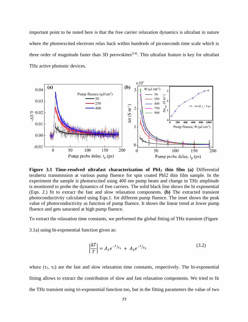
77
important point to be noted here is that the free carrier relaxation dynamics is ultrafast in nature
where the photoexcited electrons relax back within hundreds of picoseconds time scale which is
three order of magnitude faster than 3D perovskites[14]. This ultrafast feature is key for ultrafast
THz active photonic devices.
Figure 3.1 Time-resolved ultrafast characterization of PbI2 thin film (a) Differential
terahertz transmission at various pump fluence for spin coated PbI2 thin film sample. In the
experiment the sample is photoexcited using 400 nm pump beam and change in THz amplitude
is monitored to probe the dynamics of free carriers. The solid black line shows the bi exponential
(Eqn. 2.) fit to extract the fast and slow relaxation components. (b) The extracted transient
photoconductivity calculated using Eqn.1. for different pump fluence. The inset shows the peak
value of photoconductivity as function of pump fluence. It shows the linear trend at lower pump
fluence and gets saturated at high pump fluence.
To extract the relaxation time constants, we performed the global fitting of THz transient (Figure
3.1a) using bi-exponential function given as:
|∆𝑇
𝑇| = 𝐴1𝑒
−𝑡 𝜏1⁄ + 𝐴2𝑒−𝑡 𝜏2⁄
(3.2)
where (τ1, τ2) are the fast and slow relaxation time constants, respectively. The bi-exponential
fitting allows to extract the contribution of slow and fast relaxation components. We tried to fit
the THz transient using tri-exponential function too, but in the fitting parameters the value of two

78
different time constants came identical which suggest that bi-exponential function is the best fit
for this. Further, to identify the nature of recombination, we performed fluence dependent
dynamics, and the fitting revealed that the fast component “τ1” decreases from 12.8 ± 1 to 8.2 ±
0.6 ps by increasing the pump fluence (Φ) from 50 to 400 µJ/cm2. This decrease in time constant
suggest that the fast relaxation process is Auger recombination, as Auger process is directly
proportional to the number densities. Increasing the pump fluences increase the carrier densities
which in turn facilitate the faster relaxation process via Auger recombination. Figure 3.1b shows
the transient photoconductivity (∆σ) extracted using Eq. 1. The extracted photoconductivity
value varies in the order of ~ 103 S/m which ensures the excellent photoconductive nature of PbI2
thin film. Increasing the pump fluence increases the photoconductivity. Inset shows the peak of
∆σmax as function of pump fluence which suggest that ∆σmax increases linearly with pump fluence
till 400 µJ/cm2 and starts getting saturated at higher pump fluence. Thus, operating below 400
µJ/cm2 ensures that there won’t be any nonlinear effects in the PbI2 thin film. The number 400
µJ/cm2 is not very specific, it may vary from thickness and morphology (i.e. film quality) of the
film. After characterizing the ultrafast feature of PbI2 thin film, we next integrate it with THz
metamaterial to realize active control of THz waves which is essential for THz based
applications.
3.3 PbI2 integrated hybrid metadevice
The advent of metamaterials (MMs) has allowed the advance manipulation of THz waves such
as amplitude, phase and polarization[22]. MMs are topologically flat, functionally versatile and
spectrally scalable. However, the optical properties of these MMs are static once they fabricated
that put constraint for many applications. Thus, it of desire to tune the optical properties of MMs
79
actively by external means. In this section, we describe the active modulation of THz waves by
integrating MM structure with PbI2 thin film. The first part of section (i.e. 3.3.1) is devoted to
THz MM that exhibits Fano resonance and its advantages. In the next section (3.3.2), we present
all optical ultrafast active modulation of THz in PbI2 spin-coated hybrid metadevice. Further, the
effect of optical pump fluence and the effect of thickness of PbI2 on Fano resonance modulation
are investigated in section 3.3.3.
In the quest of developing active metadevice, many approaches have been demonstrated like
mechanical[10], electrical and integrating with semiconductors[23, 24] and superconductors[9]. Each
of these approaches has its advantage and limitations and should be chosen appropriately
depending on the required applications. For example, electrical and mechanical based active
control exhibit slow switching speed so can’t be used for high-speed modulator in
communication scenario. Similarly, superconductor-based approach cannot be used for large
scale applications due to cost restriction. Integrating the semiconductor offers vast range of
options as we can choose the semiconductors smartly depending on the applications. Since, our
aim is to develop high-speed THz modulators which could be used in next generation high-speed
wireless communication, thus, the integration of PbI2 with metamaterials opens up a potential
avenue.
3.3.1 THz Fano resonator
In chapter 2, we discussed the basic physics of metamaterial. In this work, we choose
asymmetric split ring resonator, which we call as terahertz asymmetric split ring (TASR)
resonator throughout in this chapter. The TASR is a ring resonator with dual split capacitive gaps
on opposite arms, and one of the gaps is displaced from the central position to create the
80
structural asymmetricity as shown in Figure 3.3a. When a terahertz waves with the electric field
polarized perpendicular to the gap incidence, a sharp asymmetric Fano resonance along with
broad dipole resonance are excited as shown in Figure 3.2a. The Fano resonator consists of two
near field coupled dipole resonators with broken structural symmetry, defined by the asymmetry
parameter, ‘d’. The broad dipole resonance of the individual resonator acts as the bright
continuum which manifests as parallel surface currents at both the arms as shown in Figure 3.2b,
while the broken symmetry encompasses the dark mode. When the dipole resonators are
perfectly symmetric, Fano resonance ceases to exist (Red solid line, Figure 3.2a). Upon
introducing the small structural asymmetry between the resonators, a sharp asymmetric line-
shaped Fano resonance appears due to interference between sharp discrete resonance and much
broader continuum-like dipole resonance as shown in Figure 3.2a, solid black line. The narrow
linewidth of Fano resonance arises due to suppressed radiation mode. The structural
asymmetricity leads to weak coupling to free space which results strongly suppression of
radiation losses. In addition to high Q the circulating surface currents is also the characteristic
feature of Fano resonance which is shown in Figure 3.2b. With increasing asymmetry, the Fano
resonance strength increases, while the quality factor decreases. Hence, at the optimal
asymmetry of d = 15 µm, the figure-of-merit in terms of resonance strength and terahertz field
confinement is maximum. Hence, Fano resonators with d = 15 µm is chosen as the resonator
design.

81
Figure 3.2: (a) Simulated transmission spectra for symmetric (red solid line) and asymmetric
(black solid line) resonator. (b) Surface current distribution at Fano resonant and dipole
frequency. At Fano resonance the surface current forms close loop that results as out of plane
magnetic dipole. While at the other end, surface currents at dipole resonance frequency are
symmetric in nature.
In our study, Fano resonance is selected owing to its high Q response that enables enhanced
sensitivity to an external perturbation. The proposed metamaterial consists of a 2D periodic array
of Fano resonators made of 200 nm thick aluminum (Al) on z-cut quartz substrate as shown in
Figure 3.3a. The geometrical dimensions of the Fano resonator are as follows – square
periodicity, px = py = p = 75 µm, length (l) = 60 µm, width (w) = 6 µm, gap (g) = 3 µm and
asymmetry (d) = 15 µm as shown in the inset of Figure 3.3a.
3.3.2 Active modulation of THz in PbI2 integrated hybrid metadevice
The artistic schematic of PbI2 coated hybrid metasurface is shown in Figure 3.3a, where the PbI2
is spin coated on the top of TASR fabricated on z-cut quartz. The optical image of PbI2 coated
hybrid metadevice i.e. PbI2-TASR is shown in the inset of Figure 3.3a. The PbI2 thin film covers
the entire metasurface allowing it to uniformly influence the localized THz electric field in the
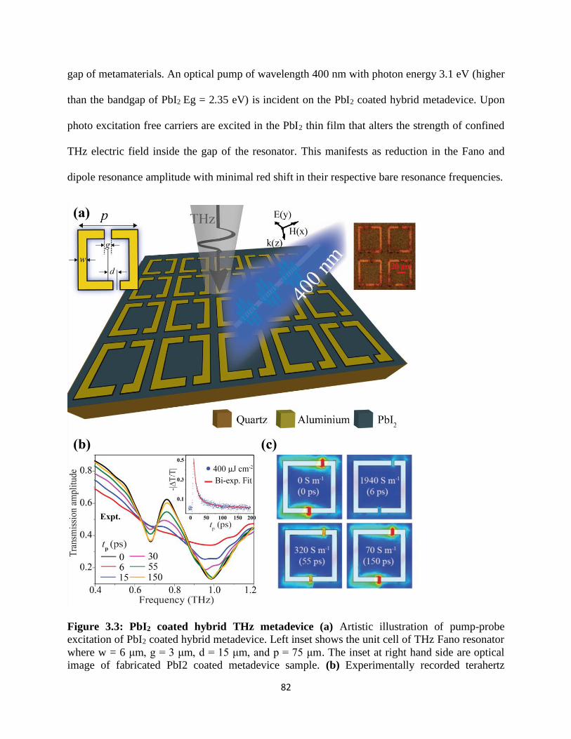
82
gap of metamaterials. An optical pump of wavelength 400 nm with photon energy 3.1 eV (higher
than the bandgap of PbI2 Eg = 2.35 eV) is incident on the PbI2 coated hybrid metadevice. Upon
photo excitation free carriers are excited in the PbI2 thin film that alters the strength of confined
THz electric field inside the gap of the resonator. This manifests as reduction in the Fano and
dipole resonance amplitude with minimal red shift in their respective bare resonance frequencies.
Figure 3.3: PbI2 coated hybrid THz metadevice (a) Artistic illustration of pump-probe
excitation of PbI2 coated hybrid metadevice. Left inset shows the unit cell of THz Fano resonator
where w = 6 μm, g = 3 μm, d = 15 μm, and p = 75 μm. The inset at right hand side are optical
image of fabricated PbI2 coated metadevice sample. (b) Experimentally recorded terahertz

83
transmission at different pump-probe delay time from PbI2 coated hybrid metadevice sample.
The pump fluence of optical pump beam was kept 400 uJ/cm2 as it was enough to switch off the
amplitude of Fano resonance completely. The inset shows the free carrier dynamics fitted with
bi-exponential (red solid line) of PbI2 thin film measured using time-resolved THz spectroscopy
at 400 uJ/cm2. (c) Simulated electric field distribution in PbI2 coated hybrid metadevice at
different conductivity of PbI2 thin film. 0 ps represents the case when pump is not arrived with
probe pulse thus resulting as 0 S/m photoconductivity. At 6 ps, the pump and probe arrive at
sample simultaneously resulting as high photoconductivity which quenches the Fano resonance
that manifests as no electric field confinement. As the free carrier relax back to equilibrium the
strength of confined electric field retrieves back.
We used the OPTP experiment setup (details are discussed in chapter 2) to characterize the
metadevice. The ultrafast modulation characteristics are shown by the measured terahertz
transmission spectra at different time instants of the pump-probe delay time (tp) starting from the
position, where pump beam has not yet arrived (tp < 0 ps) to the complete recovery (steady) state
of the system (tp ~ 150 ps). Before the optical excitation (at tp < 0 ps) of the PbI2 sample, the
structure exhibits the strongest Fano and dipole resonances (black line Figure 3.3b). Once the
sample is photoexcited, the Fano resonance (near 0.7 THz) shows complete switch-off at tp = 6
ps after the arrival of the optical pulse at the sample, where the photoexcitation of the PbI2 is the
maximum (red line Figure 3.3b). At the same time dipole resonance (near 1 THz) shows the
amplitude modulation of nearly 50 %. Once the recombination of photocarriers in PbI2 thin film
reaches the steady state equilibrium (tp ~ 150 ps), both the Fano and dipole resonance features
are fully recovered to their original strengths, thereby showing profound and complete
modulation of the Fano resonance feature of the metasurface (orange line Figure 3.3b). The
pump fluence of optical beam was 400 µJ/cm2.
Figure 3.3c shows the simulated electric field at Fano resonant frequency for different
photoconductivity of PbI2. The electric fields are simulated using CST microwave studio under
the unit cell boundary condition offered by the frequency domain solver (more details on the
simulations are given in chapter 2). By tuning the conductivity of PbI2, the strength of the

84
confined fields in the gaps is adequately controlled at the ultrafast time scales. To simulate the
electric field confined at various photoconductivity of PbI2 thin film, we used the experimentally
extracted photoconductivity at pump fluence 400 µJ/cm2 as shown in Figure 3.1b (solid blue
line). The ultrafast modulation of Fano resonance amplitude is reflected in the ultrafast switch-
off and recovery of the confined electric fields present in the resonator gaps with respect to
change in the conductivity of the PbI2 thin film. Since the fields are sensitive to the screening
effect from the photoexcited electrons, they are annihilated when the conductivity of the film is
high σPbI2 = 1940 S/m (tp = 6 ps) (as can be seen in Figure 3.1b) and are recovered to their
maximum strength in 150 ps (70 S/m).
3.3.3 Effect of optical pump fluence and thickness of PbI2
Alongside the ultrafast modulation of the Fano resonance spectra, we study the influence of
pump fluence and thickness of the PbI2 thin film on modulation (M) depth of Fano resonance
and sensitivity of the device. Before explaining the results, let's define the modulation depth (M).
In rest of this chapter, the modulation depth (M) of the Fano resonance is calculated using the
expression, 𝑀 =𝑇𝑛𝑝 − 𝑇 𝑝
𝑇𝑛𝑝 , where 𝑇𝑝 and 𝑇𝑛𝑝 are the amplitude of Fano resonance in the
transmission spectra with and without pump respectively. Figure 3.4 shows the THz transmission
spectra of PbI2 coated hybrid metadevice, where the green solid line represents the no pump case
while red solid line represents the presence of pump.

85
Figure 3.4: Terahertz transmission spectra at different pump-probe delay time. Tnp and Tp are the
amplitudes of Fano resonance representing the case of no pump and pump. It is used to calculate
the modulation (M) depth.
Figure 3.5 a-c shows the pump fluence dependent spectra for PbI2 coated metadevice for various
thickness of PbI2 thin films (160, 500 nm and 2.5 µm). The black curve in all three plots
represents the THz transmission spectrum through the bare metamaterial i.e. without PbI2
coating. It shows the Fano and dipole resonances at 0.75 THz and 1.1 THz respectively. Upon
spin coating with PbI2 thin films of various thickness, the resonances show the reduced
amplitude and redshift owing to change in the base conductivity and dielectric constants in the
vicinity of the resonators. Under the pump incidence, amplitude of the Fano and dipole
resonances decreases with increasing the pump fluence, which is also reflected as the increase in
the modulation depth (M) of the corresponding resonances. Figure 3.5 d-f shows the modulation
depths of Fano and dipole resonances for various thickness of PbI2 in PbI2-TASR. Figure 3.5d-f
reveal that, Fano follows the exponential trend, while the dipole modulation exhibits linear
response.
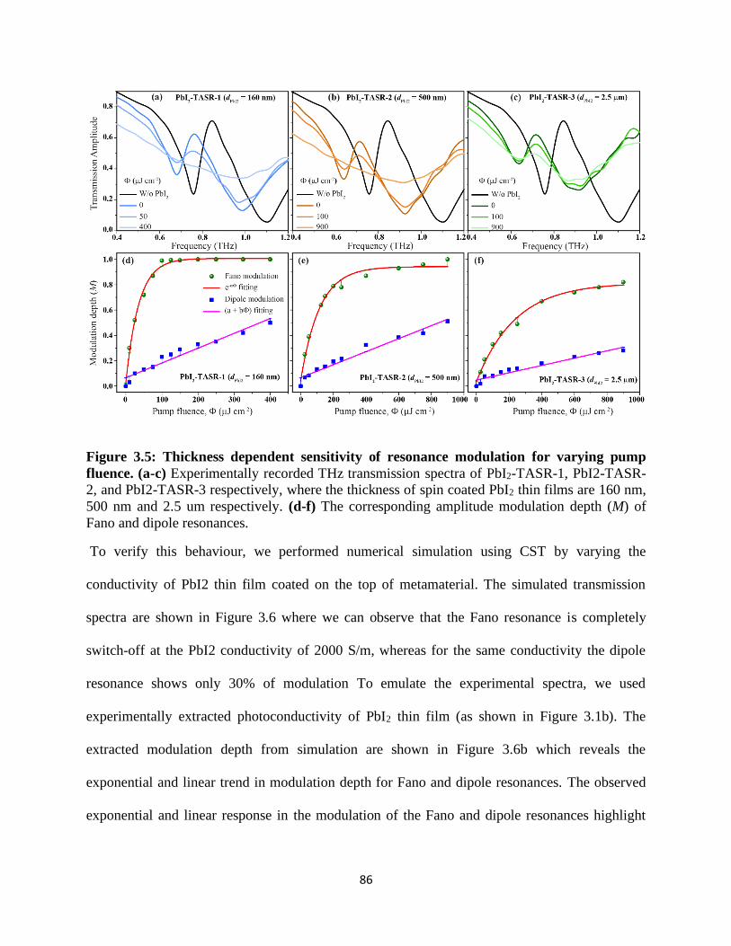
86
Figure 3.5: Thickness dependent sensitivity of resonance modulation for varying pump
fluence. (a-c) Experimentally recorded THz transmission spectra of PbI2-TASR-1, PbI2-TASR-
2, and PbI2-TASR-3 respectively, where the thickness of spin coated PbI2 thin films are 160 nm,
500 nm and 2.5 um respectively. (d-f) The corresponding amplitude modulation depth (M) of
Fano and dipole resonances.
To verify this behaviour, we performed numerical simulation using CST by varying the
conductivity of PbI2 thin film coated on the top of metamaterial. The simulated transmission
spectra are shown in Figure 3.6 where we can observe that the Fano resonance is completely
switch-off at the PbI2 conductivity of 2000 S/m, whereas for the same conductivity the dipole
resonance shows only 30% of modulation To emulate the experimental spectra, we used
experimentally extracted photoconductivity of PbI2 thin film (as shown in Figure 3.1b). The
extracted modulation depth from simulation are shown in Figure 3.6b which reveals the
exponential and linear trend in modulation depth for Fano and dipole resonances. The observed
exponential and linear response in the modulation of the Fano and dipole resonances highlight

87
the distinctive nature of their respective near-field confinement, where the strong field
confinement for Fano resonance aids higher sensitivity in resonance switching.
Figure 3.6 (a) Simulated transmission spectra for different photoconductivity of PbI2 thin film.
(b) The variation of modulation depths for Fano and dipole resonance are fitted with exponential
and linear function. The rate constant for exponential fit is α = 0.003 and slope of dipole
variation is b = 0.0019
As shown in Figure 3.5d, for the PbI2-TASR-1, where the thickness of PbI2 thin film is dPbI2 =
160 nm, shows near unity modulation at Φ = 400 µJ/cm2 pump fluence. The Fano modulation
starts to saturate at 100 µJ/cm2 owing to its exponential behaviour. While for PbI2-TASR-2 and
PbI2-TASR-3 the where the thickness of PbI2 thin films are 500 nm and 2.5 um respectively,
require high pump fluence to quench the resonances. The change in the depths of modulation
(M) for Fano resonance with respect to pump fluence is fitted with an exponential function,
𝑀𝐹𝑎𝑛𝑜 = 𝑒−𝛼𝛷 where α is the rate constant and Φ is the pump fluence, whereas the linear change
in dipole modulation is fitted using linear function, 𝑀𝑑𝑖𝑝𝑜𝑙𝑒 = 𝑎 + 𝑏𝛷 where, a is the intercept
and b is the slope of the linear fitting. The extracted rate constants (α) for Fano modulation are
0.028, 0.009, and 0.004 for the PbI2-TASR-1, PbI2-TASR-2, and PbI2-TASR-3 respectively

88
which affirms that the sensitivity and the rate of modulation are better for the PbI2-TASR-1 i.e.
metadevice with thinner PbI2 film. The modulation depth for the dipole resonance in PbI2-TASR-
1 reaches as high as 𝑀𝑑𝑖𝑝𝑜𝑙𝑒 = 0.5 at Φ = 400 µJ/cm2, whereas for in PbI2-TASR-2 and 3, the
maximum achieved modulation for dipole even at high pump fluence: Φ = 900 µJ/cm2 reaches
0.52 and 0.28 respectively. The slope of linear response for three metasurface is 0.0012, 0.0005,
and 0.00025 for increasing thickness of PbI2. The decreasing trend in slopes affirms the different
sensitivity of photoswitching. In conclusion, these results affirm that modulation of metasurface
resonances depend on the thickness of the spin coated PbI2 thin film, where the thinner films aid
ultrasensitive modulation at low pump fluences.
3.4 Effect of thickness on ultrafast dynamics
In section 3.2 we have investigated the ultrafast and high photoconductivity properties of bare
PbI2 thin film by using TRTS. Also, section 3.3 shows the influence of PbI2 thin film thickness
on the modulation depth of MM resonances. As a natural progression in the development of
active metamaterial, it is important to develop multi functionalities where we can tune the
properties of active device such as switching effect, threshold pump fluence for active
modulation. In this regard, we observed the tunability of relaxation dynamics of PbI2 thin film
when coated on MM structure by varying the thickness of PbI2 thin film. The interaction between
the localized THz field and photoexcited electrons in PbI2 thin film manifests as change in
carrier dynamics for different thickness of PbI2 thin film coated in metamaterial structure. Thus,
we devote a dedicated section to discuss the effect of thickness of PbI2 thin film on its relaxation
dynamics when coated on MM structures.
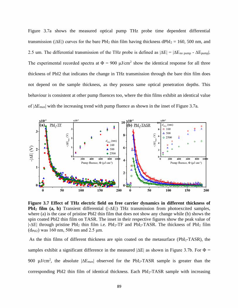
89
Figure 3.7a shows the measured optical pump THz probe time dependent differential
transmission (|∆E|) curves for the bare PbI2 thin film having thickness dPbI2 = 160, 500 nm, and
2.5 um. The differential transmission of the THz probe is defined as |∆E| = |∆Eno pump - ∆Epump|.
The experimental recorded spectra at Φ = 900 µJ/cm2 show the identical response for all three
thickness of PbI2 that indicates the change in THz transmission through the bare thin film does
not depend on the sample thickness, as they possess same optical penetration depths. This
behaviour is consistent at other pump fluences too, where the thin films exhibit an identical value
of |∆Emax| with the increasing trend with pump fluence as shown in the inset of Figure 3.7a.
Figure 3.7 Effect of THz electric field on free carrier dynamics in different thickness of
PbI2 film (a, b) Transient differential (|-∆E|) THz transmission from photoexcited samples,
where (a) is the case of pristine PbI2 thin film that does not show any change while (b) shows the
spin coated PbI2 thin film on TASR. The inset in their respective figures show the peak value of
|-∆E| through pristine PbI2 thin film i.e. PbI2-TF and PbI2-TASR. The thickness of PbI2 film
(dPbI2) was 160 nm, 500 nm and 2.5 μm.
As the thin films of different thickness are spin coated on the metasurface (PbI2-TASR), the
samples exhibit a significant difference in the measured |∆E| as shown in Figure 3.7b. For Φ =
900 µJ/cm2, the absolute |∆Emax| observed for the PbI2-TASR sample is greater than the
corresponding PbI2 thin film of identical thickness. Each PbI2-TASR sample with increasing

90
thickness of PbI2 thin film exhibits a decrease in |∆Emax|, thus signifies the film thickness
dependent change in the THz transmission. Again, we want to highlight that for the given pump
fluence “Φ” the value of |∆Emax| is high for 160 nm coated TASR as shown in the inset of the
Figure 3.7b. This suggests the fact that TASR coated with the thinnest film are more sensitive
towards external perturbation.
To unravel the reason behind the thickness dependent dynamics, we look into the THz field
confinement in TASR. At Fano resonance frequency there exists THz electric field confined in
the capacitive gap of the TASR as shown in Figure 3.3c. In addition to in-plane confinement, this
electric field exponentially extends out of plane (i.e. in both directions perpendicular to the
substrate). Thus, the interaction of this confined THz electric field acts as a probe in the OPTP
measurement. Based on the interaction volume with PbI2 thin film, the observed dynamics can be
divided as surface dynamics and bulk dynamics. Similar strategy has been followed to isolate the
surface carrier dynamics from the bulk dynamics in GaAs and InP thin film using THz
nanoprobing technique[25]. For 160 nm PbI2 thin film the interaction volume of THz probe is
high compared to 500 nm and 2.5 um thick films thus the observed carrier dynamics in 160 nm
coated thin film contains the bulk as well as surface dynamics as also discussed in[25]. While on
the other hand the carrier dynamics for 500 nm and 2.5 um PbI2 thick film majorly contains the
surface dynamics thus faster in nature as shown in Figure 3.7b. The thickness dependent ultrafast
properties of PbI2-TASR hybrid device can also be quantified by Purcell factor due to resonant
nature of TASR. The Purcell factor for the metamaterial cavity can be calculated as 𝐹𝑝 =
3
4𝜋2(λ
n)3
(Q
V), where λ is the wavelength of confined electric field, n is the refractive index of
thin-film, Q is the quality factor of metamaterial cavity and V is the cavity volume. For our
TASR, the calculated Purcell factor 𝐹𝑝 for Fano (λ = 440 μm) and dipole (λ = 300 μm)
91
resonances are 1080 and 6 respectively. The strong field confinement at Fano resonance
frequency results to higher Purcell factor thus strong interaction with PbI2 thin film and modifies
the surface properties of the photoexcited thin film.
In conclusion, this chapter discusses about the photo-physics of PbI2 thin film, where time-
resolved THz spectroscopic measurement reveals the ultrafast feature of photo excited free
carriers which relax back within 150 ps time scale. Further, integrating the PbI2 thin film with
TASR enable ultrasensitive and ultrafast THz modulators which is vital for the next generation
THz wireless communication. PbI2 integrated hybrid metadevice (PbI2-TASR) exhibits near
unity modulation of THz electric field at optical pump fluence (Φ = 400 µJ/cm2) with 150 ps
switching time speed. The thickness of PbI2 plays an important role towards the sensitivity and
ultrafast feature of PbI2-TASR. The thinner PbI2 film showed low threshold switching and high
photoconductivity while on the other hand thick PbI2 film exhibits faster switching speed owing
to domination of surface dynamics detected by THz probe. The development of on-demand
manipulation of carrier dynamics is of high interest to realize advance level functionalities of
THz based devices. Thus, altering the ultrafast switching time of PbI2-TASR hybrid metadevice
by varying the thickness of spin coated PbI2 film provides a novel platform to realize most-
efficient, reusable, cost-effective, sensitive, and real-time tunable ultrafast all optical THz
modulators. The design of optimized Q/V THz cavities could also play an important in altering
the semiconductor dynamics quoted on it. In chapter X, we have discussed few strategies to
design metadevice with on-demand altering the switching time, which is useful for next-
generation high-speed THz wireless communication and THz based ultrasensitive sensors.
3.5 References [1] I. F. Akyildiz, J. M. Jornet, C. Han, Physical Communication 2014, 12, 16.
[2] J. Federici, L. Moeller, Journal of Applied Physics 2010, 107, 111101.

92
[3] K. Ajito, Y. Ueno, IEEE Transactions on Terahertz Science and Technology 2011, 1, 293. [4] J. Darmo, V. Tamosiunas, G. Fasching, J. Kröll, K. Unterrainer, M. Beck, M. Giovannini, J.
Faist, C. Kremser, P. Debbage, Opt. Express 2004, 12, 1879.
[5] Y. Xiang, J. Zhu, L. Wu, Q. You, B. Ruan, X. Dai, IEEE Photonics Journal 2018, 10, 1.
[6] P. Pitchappa, M. Manjappa, C. P. Ho, R. Singh, N. Singh, C. Lee, Advanced Optical Materials 2016, 4, 541.
[7] W. X. Lim, M. Manjappa, Y. K. Srivastava, L. Cong, A. Kumar, K. F. MacDonald, R. Singh,
Advanced Materials 2018, 30, 1705331. [8] P. Pitchappa, A. Kumar, S. Prakash, H. Jani, T. Venkatesan, R. Singh, Advanced Materials 2019,
31, 1808157.
[9] Y. K. Srivastava, M. Manjappa, L. Cong, H. N. S. Krishnamoorthy, V. Savinov, P. Pitchappa, R. Singh, Advanced Materials 2018, 30, 1801257.
[10] X. Liu, W. J. Padilla, Advanced Optical Materials 2013, 1, 559.
[11] S. A. Veldhuis, P. P. Boix, N. Yantara, M. Li, T. C. Sum, N. Mathews, S. G. Mhaisalkar,
Advanced Materials 2016, 28, 6804. [12] G. Xing, N. Mathews, S. S. Lim, N. Yantara, X. Liu, D. Sabba, M. Grätzel, S. Mhaisalkar, T. C.
Sum, Nature Materials 2014, 13, 476.
[13] L. Li, Y. Deng, C. Bao, Y. Fang, H. Wei, S. Tang, F. Zhang, J. Huang, Advanced Optical Materials 2017, 5, 1700672.
[14] M. Manjappa, Y. K. Srivastava, A. Solanki, A. Kumar, T. C. Sum, R. Singh, Advanced Materials
2017, 29, 1605881. [15] A. F. d. Silva, N. Veissid, C. Y. An, I. Pepe, N. B. d. Oliveira, A. V. B. d. Silva, Applied Physics
Letters 1996, 69, 1930.
[16] S. Roth, W. R. Willig, Applied Physics Letters 1971, 18, 328.
[17] M. Matuchová, K. Žďánský, M. Svatuška, J. Zavadil, O. Procházková, Chemical Papers 2007, 61, 36.
[18] L. Wang, C. McCleese, A. Kovalsky, Y. Zhao, C. Burda, Journal of the American Chemical
Society 2014, 136, 12205. [19] T. J. Jacobsson, J.-P. Correa-Baena, E. Halvani Anaraki, B. Philippe, S. D. Stranks, M. E. F.
Bouduban, W. Tress, K. Schenk, J. Teuscher, J.-E. Moser, H. Rensmo, A. Hagfeldt, Journal of the
American Chemical Society 2016, 138, 10331.
[20] J. S. Yun, J. Seidel, J. Kim, A. M. Soufiani, S. Huang, J. Lau, N. J. Jeon, S. I. Seok, M. A. Green, A. Ho-Baillie, Advanced Energy Materials 2016, 6, 1600330.
[21] L. M. Herz, Annual Review of Physical Chemistry 2016, 67, 65.
[22] Y. Liu, X. Zhang, Chemical Society Reviews 2011, 40, 2494. [23] W. J. Padilla, A. J. Taylor, C. Highstrete, M. Lee, R. D. Averitt, Physical Review Letters 2006,
96, 107401.
[24] J. Gu, R. Singh, X. Liu, X. Zhang, Y. Ma, S. Zhang, S. A. Maier, Z. Tian, A. K. Azad, H.-T. Chen, A. J. Taylor, J. Han, W. Zhang, Nature Communications 2012, 3, 1151.
[25] G. Choi, Y.-M. Bahk, T. Kang, Y. Lee, B. H. Son, Y. H. Ahn, M. Seo, D.-S. Kim, Nano Letters
2017, 17, 6397.

93
Chapter 4
Excitons in 2D perovskites for ultrafast
terahertz photonic devices
In chapter 3, we discussed about PbI2 based all-optical ultrafast terahertz (THz) metadevice,
which showed 150 ps (~ 6.7 GHz) switching speed at Φ = 400 μJ/cm2 optical pump fluence. This
remarkable ultrafast control on THz waves opens the avenue for the development of the solution-
processed semiconductor based ultrafast THz metadevice. However, the development of ultrafast
THz devices is still at the heart of many practical applications such as high-speed wireless
communications. To give a perspective, in the wireless communication, modulators are the key
component that decides the data transfer speed. Thus, switching the THz electric field with GHz
modulation speed restrict the data transfer rate in gigabits per second range. Thus, switching the
THz waves with high-speed will enhance the data transfer speed.
In this chapter, we will discuss 2D perovskite-based ultrafast terahertz photonic devices, where
the ultrafast feature arises due to self-assembled quantum well structures in 2D perovskites.
Further, we unravel the photo-physics of 2D perovskite including free carriers and exciton
dynamics using time-resolved THz spectroscopy (TRTS).
4.1 Introduction
In recent years, organic-inorganic hybrid three-dimensional (3D) perovskites have seen
unprecedented rapid development owing to their outstanding optoelectronic properties such as

94
larger diffusion lengths, excellent charge carrier mobilities, bandgap tunability, high optical gain,
and nonlinear response along with low fabrication cost[1-5]. However, their instability in ambient
conditions hinders their large-scale applications[6, 7]. In contrast, 2D Ruddlesden Popper (RP)
perovskites offer better opportunities compared to their 3D counterparts[8, 9]. Their excellent
ambient stability, along with abundant tunable optoelectronic properties and high quantum
efficiency, makes them ideal for a wide range of electronic and optical applications[10-13]. In the
recent times, RP perovskites have shown excellent efficiency for light-emitting diode (LED)[8,
14]. The existence of self-assembled quantum wells (QWs) due to alternative arrangement of
organic and inorganic atomic layers provides an additional relaxation pathway for the
photoexcited free carrier to relax back at ultrafast time scales, that makes them a perfect
candidate for ultrafast active photonic devices[5, 15, 16]. Since past few decades, there has been
huge demand for ultrafast tunable devices at terahertz (THz) frequencies owing to their wide
range of disruptive applications ranging from imaging, sensing and high-speed wireless
communications[17-20]. To achieve unprecedented control over THz waves, metamaterials (MMs)
have been extensively used due to their structural simplicity and tunable optical properties[21, 22].
Furthermore, integrating the MMs with semiconductors offer a unique platform to dynamically
control and manipulate the THz waves.
Recently, many developments have focused on developing the active MMs by integrating with
dynamic materials such as liquid crystals[23, 24], semiconductors[25-28] (e.g. Si, GaAs etc),
superconductors[29], graphene[30], and microelectromechanical systems[31] where the intrinsic
properties of MMs can be modulated by external stimuli such as voltage bias, optical light,
electrical bias, and temperature. However, among these approaches translating them for large
scale practical applications require either huge cost investment or advance level fabrication.

95
Thus, solution-processed semiconductors are a viable alternative that provides ease of integration
with diverse range of optoelectronics functionalities. On the other hand, split ring resonators are
the most commonly studied meta-atoms owing to its structural simplicity and ease of tuning
optical parameters by structural reconfiguration[32]. In this study we employed, asymmetric split
ring resonator that exhibits high field confinement due to excitation of non-radiative mode which
is known as Fano resonance owing to its asymmetric line shape in the transmission spectra[33-35].
In chapter 3 we discussed about the terahertz split ring resonator (TASR) and its surface current
characteristic for different resonances. Thus, we opted TASR due to Fano resonance and its
strong sensitivity towards the surrounding medium as a metadevice for studying the 2D
perovskite based ultrafast THz devices.
In this chapter, we report a facile ultrafast THz photonic device by integrating 2D perovskites
with THz metamaterial for advanced manipulation of THz waves. The existence of QWs in the
2D perovskite thin film offers stable excitons at room temperature. Thus, the presence of QWs
provides an additional relaxation channel to the photoexcited free carrier that manifests as
ultrafast relaxation. The synergic relation between 2D perovskite with scalable metamaterials
offer an efficient active metamaterial with enhanced optical features. In this work, we explore the
free carrier as well as exciton dynamics using time-resolved THz spectroscopy (TRTS).
Furthermore, we demonstrate an ultrafast active metadevice using solution-processed 2D
perovskite thin film spin coated over TASR. Here, we achieve 93% modulation of Fano
resonance amplitude, showing ultrafast switching times of 20 ps (i.e., ~ 50 GHz modulation
speed) which is fastest for the solution processed semiconductor-based hybrid metadevice.

96
4.2 Structural and optical characterization of 2D perovskite thin
film
The general formula for Ruddlesden-Popper (RP) perovskites family is (RNH3)2An-1MnX3n+1
where RNH3 is an organic cation; A is monovalent organic cation; M is a divalent metal cation,
X is a halide anion and n represent the number of [MX6]4- octahedral layers sandwiched between
organic cation layers. Since the density of QWs decreases by increasing the layers of 2D
perovskites (n). Thus, as control reference we used n = 1, 2 and ∞ (i.e. 3D perovskite). The
chemical formula for n = 1, 2, and ∞ are C6H5(CH2)2NH3)2PbI4 or ((PEA)2PbI4),
((C6H5(CH2)2NH3)2)2(CH3NH3) PbI7) and CH3NH3PbI3 respectively. The AFM image for all
these films were measured to confirm the good quality of the films and presented in
Appendix A. Structurally, in pure 2D perovskite film the two-consecutive lead iodide
octahedral layers [MX6]4- are separated by two layers of large organic spacer cations, which
are held together via weak Van der Waals forces. The octahedral structure of lead halide leads
to the low energy barrier for the charge carriers while poor conductivity of organic spacer
leads to the high energy barrier and thus form the QW structure as shown in Figure 4.1a.
While n = 2 contains stacks of organic and inorganic layers supporting both in-plane and bulk
transport of charge carrier. In 3D, each layer of [MX6]4- octahedral connected with six
neighbors at halogen atoms that forms a network where small organic cations located at the
void of the network[5] as shown in Figure 4.1c.

97
Figure 4.1 Charge transport in different dimensioned perovskite (a) shows the in-plane
charge transport in 2D perovskite. The out of plane movement of free carriers is restricted due to
insulating organic barrier. (b) in mixed 2D and 3D perovskite both the in-plane and out of plane
motion of free carrier are allowed. (c) 3D perovskite facilitates the charge transport through bulk.
The existence of QWs structure in 2D perovskites makes it unique in the solution-processed
semiconductor family. Excitons are formed with high binding energy (Eb – 0.1-0.5 eV)[9] in
2D perovskite due to low dielectric screening from the surrounding organic ligands and
electrons and holes get confined within the 2D inorganic lattices[36]. Due its unique structural
arrangement, 2D perovskite offer unique spatial redistribution of photogenerated species that
is vital for the development of multifunctional active metadevice. By changing the 2D
perovskite layer the charge carrier dynamics can be altered. For instance, Blancon et al.
showed that there exists an “edge states”[37] at the interface of perovskite layers for n > 2 as
shown in Figure 4.2a. The unique feature of these “edge states” is that it provides a direct
pathway for dissociating excitons into longer-lived free carriers. Such dissociated free carriers
are expected to be protected from nonradiative decay channel thus contribute to the
photocurrent in solar cells or radiative recombination for LED applications. The presence of
these edge states alters the carrier dynamics from fast recombination to slow recombination,
thus the integration of different layered 2D perovskite i.e. with different n can enable active
THz metadevice with various range of switching speed ranging from picosecond to
nanoseconds. In addition to this unique feature the presence of QWs aids the ultrafast

98
relaxation to the photo excited free carrier. In this study we have taken the advantage of this
remarkable feature of 2D perovskite for ultrafast THz photonic devices.
Figure 4.2 Various unique properties of 2D perovskite (a) shows the existence of edge states
in 2D perovskite for n > 2. The existence of this edge states increases the lifetime of free carrier
and protected from nonradiative decay. The detailed discussion is given in [37]. (b) The existence
of quantum well (QW) in 2D perovskite where inorganic layers act as potential well and organic
layers serve as potential barriers. (c) Comparison of free carrier dynamics (normalized) for 2D,
mixed 2D and 3D and pure 3D perovskite. The presence of QW in 2D perovskite provides an
additional relaxation channel for the photoexcited free carrier as compared to other alternative
that manifests as ultrafast relaxation.
Figure 4.2b shows the schematic of QW structure formed by altering semiconductor inorganic
layers and organic layers. The excitons are formed inside the QW with binding energy ranging
from 0.1-0.5 eV[9]. Photoexciting with optical pump beam with energy above the bandgap of
perovskite generates free carriers. We employed Optical Pump and Terahertz Probe (OPTP)
spectroscopic technique to monitor the free carrier relaxation dynamics. We discussed the detail
of OPTP in chapter 2. Figure 4.2c shows the normalized free carrier dynamics measured using
OPTP for 2D, mixed 2D -3D and 3D perovskites. Increasing “n” reduces the density of QWs
thus the additional relaxation channel for photo excited free carrier reduces as result we observe
slow relaxation while moving from 2D to 3D as shown in Figure 4.2c. All the samples were
photoexcited above the bandgap (Eg, 3D = 1.5 eV, Eg, 3D-2D = 1.8 eV, Eg, 2D = 2.2 eV) with 400
nm (E = 3.1 eV) optical pump beam and THz waves used as probe to record the free carrier
relaxation dynamics. Pumping the 2D perovskite above the bandgap generates free carriers and
99
excitons. We employed OPTP to unveil the dynamics of free carriers as well as excitons. In
OPTP experiment the attenuation in the peak amplitude of THz waves is proportional to the real
part of photoconductivity which mostly arise due to in-phase motion of free electrons with THz
electric fields[38, 39]. The free carrier dynamics is recorded by monitoring the change in peak
amplitude of THz waves by varying pump delay time. A translational delay stage with
micrometers spatial precision is used for inducing delay between pump and probe. The detailed
experimental procedure of OPTP measurements are discussed in chapter 2. In contrast, the
presence of excitons or bound electrons induces a phase shift in THz waves which is
proportional to the imaginary part of photoconductivity. Thus, by monitoring the change in THz
amplitude at zero crossing of THz pulse gives the excitons dynamics[38-40]. In order to validate
that the presence of excitons in 2D perovskite induces phase shift, we recorded differential
change in THz electric field as shown in Figure 4.3a. The phase shift in differential THz electric
field ensures that each point has been phase shifted due to presence of excitons. Figure 4.3 shows
the differential change in THz electric field (Red solid line) at τpump = 1.5 ps. It is clearly evident
that the present of excitons induced phase shift in the THz pulse thus monitoring the change in
THz amplitude at zero crossing reflects the exciton dynamics.
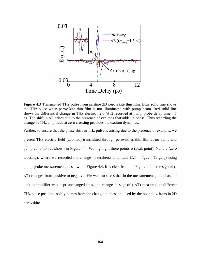
100
Figure 4.3 Transmitted THz pulse from pristine 2D perovskite thin film. Blue solid line shows
the THz pulse when perovskite thin film is not illuminated with pump beam. Red solid line
shows the differential change in THz electric field (∆E) recorded at pump probe delay time 1.5
ps. The shift in ∆E arises due to the presence of excitons that adds up phase. Thus recording the
change in THz amplitude at zero crossing provides the exciton dynamics.
Further, to ensure that the phase shift in THz pulse is arising due to the presence of excitons, we
present THz electric field (zoomed) transmitted through perovskites thin film at no pump and
pump condition as shown in Figure 4.4. We highlight three points a (peak point), b and c (zero
crossing), where we recorded the change in terahertz amplitude (∆T = Tpump -Tno pump) using
pump-probe measurement, as shown in Figure 4.4. It is clear from the Figure 4.4 is the sign of (-
∆T) changes from positive to negative. We want to stress that in the measurements, the phase of
lock-in-amplifier was kept unchanged thus, the change in sign of (-∆T) measured at different
THz pulse positions solely comes from the change in phase induced by the bound excitons in 2D
perovskite.

101
Figure 4.4 Effect of phase change induced by exciton in THz amplitude where the change in
sign of (-∆T = Tpump – Tno pump) changes from positive to negative from point “a” to “c”. The THz
pulse shifts due to presence of excitons which induces the negative sign of (-∆T) at zero
crossing.
Figure 4.5a represents the 3D color plot of ∆T at different THz pulse position (shown as blue
dots in Figure 4.5b). In 3D plot, the gradual change in color represents the change in sign of (-
∆T) from positive (measured at peak position, marked as (i) in Figure 4.5b) to negative
(measured at zero crossing, marked as (iii) in Figure 4.5b). This change in sign of (-∆T) can be
clearly explained by Figure 4.4, where at peak point (point a in Figure 4.4a) the THz amplitude
is modulated by free carrier (i.e. Tno pump > Tpump). Similarly, at point “b” there is no in amplitude
modulation (i.e. Tno pump = Tpump) and at point “c” (i.e. Tno pump < Tpump). This occur due to phase
shift in THz pulse owing to the presence of excitons. Thus, the presence of excitons set the sign
of (-∆T) to vary from positive to negative.

102
Figure 4.5 (a) 3D color plot of ∆T recorded at different THz delay position shows as blue dots in
“b”. (b) Transmitted THz pulse recorded from non-excited 2D perovskite thin film. Blue dots
represent the delay positions where change in THz amplitude (∆T) are recorded which shows the
change in sign from positive to negative while moving from point (i) to (iii)
Now we know that the presence of excitons imparts the phase shift in THz pulse. Hence using
OPTP, we monitor the dynamics of both the species (free electrons as well as excitons) in 2D
perovskite that is critical in terms of understanding the fundamental physics as well as device
applications. Figure 4.6 shows the real and imaginary part of photoconductivity at various pump
fluences recorded using time-resolved THz spectroscopy. The real of photoconductivity is
recorded by monitoring the change in THz peak amplitude by varying the pump-probe delay
time. The change in THz peak (∆Tpeak) amplitude is proportional to the free electrons number
densities thus monitoring the change in ∆Tpeak captures the free electrons dynamics. While on the
other hand monitor the change in THz amplitude at zero crossing (∆Tzero crossing) (see zero
crossing marked in Figure 4.3) mostly capture the dynamics of bound electrons or excitons as
shown in Figure 4.6b. Mathematically the real and imaginary part of photoconductivity is written
as:

103
𝛥𝜎𝑟𝑒𝑎𝑙(𝜏) =
−휀0𝑐
𝑑(𝑛𝑎𝑖𝑟 + 𝑛𝑠𝑢𝑏)
𝛥𝑇𝑝𝑒𝑎𝑘(𝜏)
𝑇
(4.1)
𝛥𝜎𝑖𝑚𝑎𝑔(𝜏) =
−휀0𝑐
𝑑(𝑛𝑎𝑖𝑟 + 𝑛𝑠𝑢𝑏)
𝛥𝑇𝑧𝑒𝑟𝑜 𝑐𝑟𝑜𝑠𝑠𝑖𝑛𝑔(𝜏)
𝑇
(4.2)
where d is the thickness of perovskite film (in our case it is 60 nm), c is the speed of light, 휀0 is
the vacuum permittivity, 𝑛𝑎𝑖𝑟 and 𝑛𝑠𝑢𝑏 are the refractive indices of air and substrate (in our case
substrate is quartz and THz refractive index is 2.1), T is the THz transmission through perovskite
thin film at no optical pump, 𝛥𝑇𝑝𝑒𝑎𝑘 and 𝛥𝑇𝑧𝑒𝑟𝑜 𝑐𝑟𝑜𝑠𝑠𝑖𝑛𝑔 are the change in THz amplitude
recorded at peak and zero crossing of THz pulse at different pump-probe delay time “𝜏” . The
detail derivation of photoconductivity from experimentally recorded THz transients are given in
Appendix A (section A2).
For clarity the plots corresponding to different pump fluence are vertically offset in Figure 4.6.
To understand the relaxation dynamics of photoexcited free carriers and excitons, THz transient
dynamics at different pump fluences are fitted using bi-exponential decay function (A1exp(-t/τ1)
+ A2exp(-t/τ2)), where τ1 and τ2 represent the time constants for the fast and slow processes,
respectively. To include the instrument response, we convoluted the bi-exponential decay
function with instrumental response function as shown:

104
𝑦 = 𝑐 + [(𝐴1𝑒−𝑥−𝑥0𝜏1 )(1 − erf (
−(𝑥 − 𝑥0 −𝑠2
𝜏1)
𝑠))]
+ [(𝐴2𝑒−𝑥−𝑥0𝜏2 )(1
− erf (−(𝑥 − 𝑥0 −
𝑠2
𝜏2)
𝑠))]
(4.3)
where 𝜏1 and 𝜏2 are the lifetimes corresponds to fast and slow process respectively and A1, A2
are their respective amplitudes, s is the erf (error function) parameter and x0, c are the axis
offsets.
Figure 4.6 Transient real and imaginary THz photoconductivity (∆σ) at different pump
fluences (a) Transient real photoconductivity recorded by monitoring the change in THz peak
amplitude at various pump fluences. (b) Transient imaginary photoconductivity recorded by
monitoring the change in THz amplitude recorded at zero crossing of THz pulse. For clarity the
graphs at various pump fluences are vertically offsets. Black solid line in a and b represent the
biexponential fit.
The extracted time constants for free electrons dynamics and excitons are shown in Table 1 and 2
respectively. In free carrier relaxation processes, the biexponential fit reveals that the initial fast

105
relaxation process is independent of pump fluences (~ 0.2 ps). The relaxation of photoexcited
free carriers follows various pathways to relax back to the equilibrium. It includes trap-assisted
monomolecular recombination, bi-molecular recombination and many-body Auger
recombination. The detailed discussion on various type of recombination are presented in
Appendix A (section A5). In the context of 2D perovskites by examining the behaviour of time
constants at various pump fluence, we identify the relaxation pathway. Since, the initial fast
relaxation process is independent of pump fluence (~ 0.2 ps), thus we attribute this fast
relaxation process to be phonon-mediated, as phonon-mediated relaxations are either
independent of pump fluence or increase with pump fluence due to hot phonon effect[41, 42].
While on the other hand the time constant for slow relaxation process decrease with pump
fluence. We attribute this to be trap-assisted relaxation because the densities of traps decrease
with increasing pump fluence. An important point to be noted here is that the slow relaxation
time (τ2) shows the ultrafast recovery, which falls in picoseconds time scales. This remarkable
feature in 2D perovskite arises due to the presence of QWs that provides an additional relaxation
channel for the photo excited free carrier. The free carriers get localized in the QWs due to
quantum confinement and form an exciton.
Following the previous studies on 2D materials and transition metal dichalcogenides, to unveil
the exciton dynamics in 2D perovskite, the measured imaginary part of photoconductivity is
fitted using biexponential decay function. The extracted time constants are shown in Table 2.
The fit reveals that both the decay time constant decrease with pump fluence. We attribute this as
many body assisted Auger recombination, as Auger assisted recombination highly depends on
carrier densities and becomes faster with an increase in pump fluences.
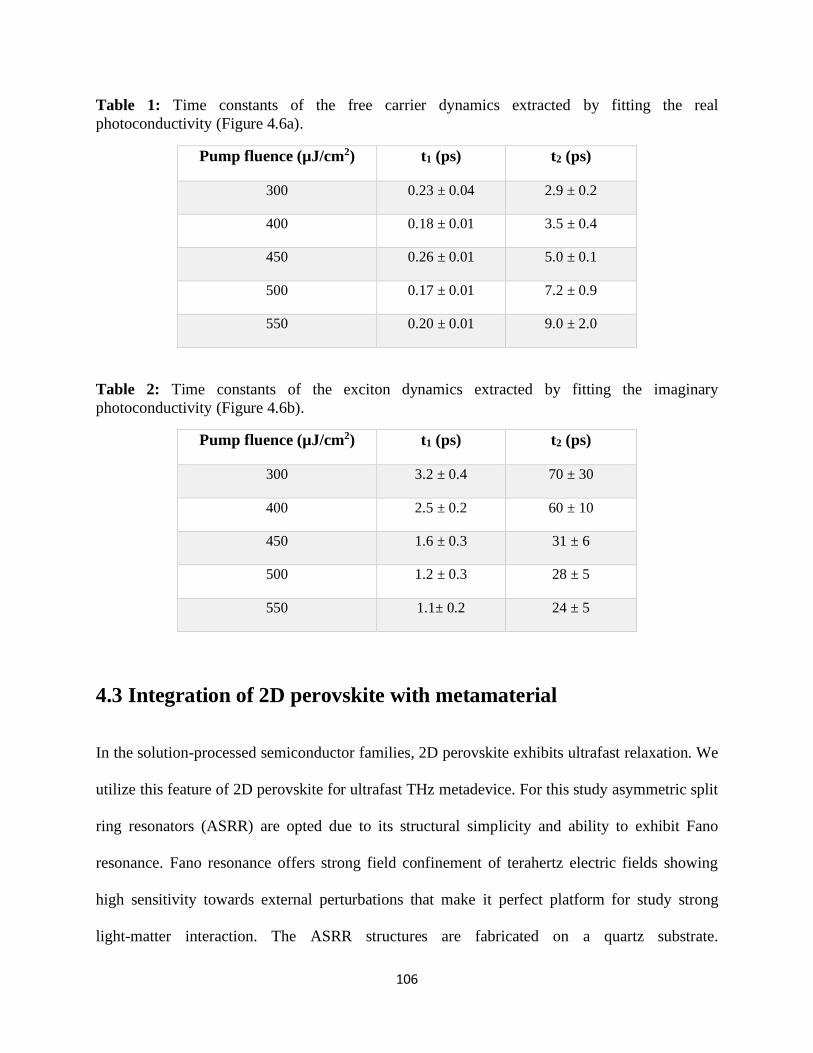
106
Table 1: Time constants of the free carrier dynamics extracted by fitting the real
photoconductivity (Figure 4.6a).
Pump fluence (µJ/cm2) t1 (ps) t2 (ps)
300 0.23 ± 0.04 2.9 ± 0.2
400 0.18 ± 0.01 3.5 ± 0.4
450 0.26 ± 0.01 5.0 ± 0.1
500 0.17 ± 0.01 7.2 ± 0.9
550 0.20 ± 0.01 9.0 ± 2.0
Table 2: Time constants of the exciton dynamics extracted by fitting the imaginary
photoconductivity (Figure 4.6b).
Pump fluence (µJ/cm2) t1 (ps) t2 (ps)
300 3.2 ± 0.4 70 ± 30
400 2.5 ± 0.2 60 ± 10
450 1.6 ± 0.3 31 ± 6
500 1.2 ± 0.3 28 ± 5
550 1.1± 0.2 24 ± 5
4.3 Integration of 2D perovskite with metamaterial
In the solution-processed semiconductor families, 2D perovskite exhibits ultrafast relaxation. We
utilize this feature of 2D perovskite for ultrafast THz metadevice. For this study asymmetric split
ring resonators (ASRR) are opted due to its structural simplicity and ability to exhibit Fano
resonance. Fano resonance offers strong field confinement of terahertz electric fields showing
high sensitivity towards external perturbations that make it perfect platform for study strong
light-matter interaction. The ASRR structures are fabricated on a quartz substrate.
107
Photolithography was used to define the Fano resonant metamaterial structures. 200 nm
Aluminium (Al) was thermally deposited and lifted off using acetone. The thin film of 2D
perovskite is spin coated on the top of fabricated metamaterial. Figure 4.7a shows the optical
image of 2D perovskite coated hybrid metadevice. The geometrical dimensions of Fano
resonators are marked in the inset of Figure 4.7c. It has a square periodicity Px = Py = P = 75
um, length (l) = 60 um, width (w) = 6 um, gap (g) = 3 um and asymmetry (x) = 15 um. Figure
4.7c shows the schematic of optical pump and terahertz probe of the 2D perovskite coated hybrid
metadevice. 400 nm is used as optical pump beam due to having energy higher than the bandgap
of 2D perovskite (Eg = 2.4 eV). Pumping the perovskite thin film above the bandgap
instantaneously generates free carriers in the conduction band that undergoes via various
relaxation channels to reach equilibrium.

108
Figure 4.7 Artistic illustration of the perovskite-coated hybrid metadevice (a) optical image
of the fabricated metadevice (b) Schematic of the quantum confinement of free carriers within
the quantum well (QW) structure of pure 2D perovskite. The quantum confinement leads to
formation stable exciton at room temperature. (c) Schematic of optical pumping scheme
illustrates the THz transmission measurement from 2D perovskite coated hybrid metadevice.
The free carrier relaxation dynamics in 2D perovskite is discussed in detail in the previous
section. The photo excited free carriers increase the conductivity of perovskite thin film and
decrease the terahertz transmission. To be more precise the conductive patch of perovskite thin
film that lies in the capacitive gap of the ASRR quench the amplitude of Fano resonance. At the
capacitive gap, the conductive patch of perovskite thin film connects both the metallic arms of
ASRR that manifests as switching off the Fano resonance in the transmission spectra. Figure 4.8

109
summarize the above-mentioned concept. Figure 4.8a shows the schematic of optical pump
excitation of 2D perovskite coated hybrid metadevice. The transmission spectra correspond to no
pump and the presence of pump case are shown in Figure 4.8b. As mentioned above the
increasing the photoconductivity of perovskite thin film shorts the capacitive gap of ASRR that
manifests as switching off the Fano resonance as shown in Figure 4.6: red solid line. The
switching behavior of Fano resonance can also be seen in terms of quenching of confined THz
field as shown in the insets of Figure 4.8b. Such active control on THz field is of great interest,
particularly in sensing and communication applications.
Figure 4.8 (a) Schematic of optical pump for 2D perovskite coated hybrid metadevice, where
400 nm is used as optical pump beam to photoexcite the free carrier in 2D perovskite thin film.
(b) Simulated THz transmission from the system architect shown in a. Black solid line shows the
Fano resonance which is simulated for ∆σ = 0 and red solid line shows the Fano switching
simulated for ∆σ = 3500 S/m. Insets show the simulated THz electric field for both the cases
where strong THz electric field is confined in the capacitive gap for Fano resonance case.
The optical characterization of 2D perovskite coated hybrid metadevice was done using ZnTe
based OPTP measurement scheme. The detailed discussion on OPTP measurements are given in

110
Chapter 2. Figure 4.7c shows the schematic of optical characterization of hybrid metadevice
where the perovskite film is photoexcited using 400 nm optical pump beam to generates
photocarrier. The frequency dependent transmission spectra at various pump fluences are shown
in Figure 4.9a. The normalized transmission spectra were calculated using 𝑇(𝜔) = |𝐸𝑠(𝜔)
𝐸𝑟(𝜔)|,
where 𝐸𝑠(𝜔) and 𝐸𝑟(𝜔) are Fourier transformed frequency domain electric field of sample and
substrate respectively. In the absence of an optical pump beam, the transmission spectra exhibit
strong asymmetric spectral profile (black solid curve, Figure 4.9a) at 0.7 THz. The strong
asymmetric line shape in the transmission spectra is the signature of Fano resonance. As
explained above, generating the free carrier quenches the amplitude of Fano resonance. Hence,
by increasing the optical pump fluence the amplitude of Fano resonance gradually reduces and
completely switch off at 250 µJ/cm2, as shown in Figure 4.9a. To emulate the experimentally
recorded spectra, we performed full-wave 3D frequency domain simulation in CST microwave
studio. In the simulation the quartz substrate is treated as lossless material with refractive index
2.1 and Al is treated as lossy metal with predefined permittivity for terahertz frequencies. The
floquet periodic boundary conditions are applied in both x and y directions to emulate the
collective response of ASRR. The simulated transmission spectra is shown Figure 4.9b that
shows close resemblence with experimentally recorded spectra (Figure 4.9a). In simulation the
perovskite thin is characterized with variable conductivity. Varying the photoconductivity in
simulation is equivalent to increasing the pump fluence in the experiment. Additionally, we
provide the simulated electric field distribution at the Fano resonance frequency (0.7 THz) for
different photoconductivity (σ) values of perovskite thin film. When σ = 0 S/m, there exists high
THz electric field confinement in the capacitive gap of ASRR as shown in Figure 4.9c. Further,

111
increase the value of σ results in a pronounced suppression of Fano resonance amplitude that
manifests as reduction in electric field strength in the capacitive gap, as shown in Figure 4.9c.
Figure 4.9 Photo switching response of the 2D perovskite-based hybrid metadevice. (a)
Experimentally measured amplitude transmission spectra recorded at various pump fluence
illustrating the switching of Fano resonance. (b) Numerically simulated THz transmission
emulating the experimental condition of a. (c) Numerically simulated electric field distribution in
hybrid metadevice for different photoconductivity values of 2D perovskite thin film.
To unveil the ultrafast feature of 2D perovskite coated hybrid metadevice, we performed the
transmission measurement at different pump-probe delay time (p). Figure 4.10a shows the
experimentally recorded transmission spectra at various p where the respective solid colors
correspond to the pump-probe delay showed using dots in the inset of Figure 4.10a. Black dot
represents the scenario when pump and probe beams are time-matched thus giving rise to
maximum change in ∆T. This results in the maximum amplitude quenching of Fano resonance as
evident in Figure 4.10 black solid line. Further, the gradual increase in Fano resonance amplitude
is evident as free carriers relax back to the equilibrium state, as shown in solid green line in
Figure 4.10a. The important point to be noted here that the recovery of Fano occurs within 20 ps
time scale. To quantify the modulation depth of Fano resonance, it is calculated as,
𝑀𝑜𝑑𝑢𝑙𝑎𝑡𝑖𝑜𝑛 (𝑀) =|𝑇𝑂𝑓𝑓− 𝑇𝑂𝑛|
𝑇𝑂𝑓𝑓 × 100 %, where Ton and Toff are the amplitude of Fano
112
resonance with and without optical pump respectively. Figure 4.10b shows the experimentally
calculated modulation depth (M) with pump fluence. We observe a systematic increment in M
with pump fluence and reach close to unity (M = 93 %) at 250 μJ/cm2. In compare to PbI2
(Chapter 3) coated hybrid metadevice the value of pump fluence is low in 2D perovskite. The
inset of Figure 4.10b shows the contour plot of amplitude modulation of Fano resonance at
different pump fluence. The color gradient shows the strength of normalized modulation. At
Fano resonance frequency (0.7 THz), the maximum modulation is achieved at 250 μJ/cm2.
Figure 4.10 Ultrafast switching of Fano resonance (a) Measured THz transmission spectra
recorded at different pump-probe delay instances. It is clear that at peak photoconductivity i.e.
black solid line (black dot in inset) the strength of Fano resonance is weak which further
strengthen when free carriers are relax to equilibrium i.e. green solid line (green dot in inset).
Inset shows the free carrier dynamics where different color dots show the pump-probe delay
instances where THz transmission is recorded and shown with same colored solid line. (b)
Amplitude modulation (M) of Fano resonance at different optical pump fluences. The contour
plot represents the amplitude modulation of Fano resonance at different pump fluence. It is
evident that modulation depth for Fano resonance is near unity.
Further to ensure the effect of optical heating on device performance, we measured the terahertz
transmission through bare perovskite thin film under the constant illumination of 400 nm optical
pump beam. We choose the pump fluence to be 300 μJ/cm2 which is slightly higher than the

113
pump fluence to achieve near unity modulation. The recorded terahertz transmission spectra are
shown in Figure 4.11a. From the Figure 4.11 it is evident that the perovskite film does not
degrade under the illumination of optical pump even at 45 min heating. This shows the
robustness of our proposed hybrid metadevice.
Figure 4.11 THz transmission through the perovskite thin film. (a) The perovskite thin film
is illuminated with 400 nm pump beam to observe the effect of optical heating. The pump
fluence is kept at 300 μJ/cm2. It is evident that the effect of optical heating is negligible in THz
transmission. (b) Effect of optical pump fluence in the THz transmission through bare z-cut
quartz
Further to eliminate any nonlinear effect from substrate (here quartz) in the range of operating
pump fluence we performed THz transmission through bare quartz substrate where quartz was
kept under 400 nm optical pump. Figure 4.11b shows the recorded THz transmission from bare
quartz substrate. It shows that quartz does not include any nonlinear absorption even at 600
μJ/cm2, which is much higher than the operating range of pump fluence i.e. ~ 250 μJ/cm2.

114
4.4 Active flexible metadevice
In the quest of developing ultrafast THz device with low cost and ease of integration, the
solution processed semiconductors specially 2D perovskite has shown promising potential. The
2D perovskite has shown low threshold switching (~ 250 μJ/cm2), high stability and ultrafast
control on THz waves. In the previous section we have shown the 2D perovskite-based hybrid
metadevice performs really well with rigid substrate (quartz in this case). In the recent years,
there has been ever increasing demand for developing flexible metadevice that has huge potential
in imaging, wearable device, flexible sensors and portable solar cells. In particular the THz
frequency region has attracted considerable attention owing to its unique properties that spans its
application domains from non-destructive imaging, material characterization to high-speed
wireless communication. To put into a perspective, in current technologies, THz images for
security applications are obtained by rotating the detectors through 3600. This makes devices
bulky and less portable. Thus, to significantly expand the usable range of THz devices for future
disruptive applications, a flexible and portable platform is vital.
In this direction, significant research has been done, such as flexible THz scanner and
detectors[43, 44]. These findings have opened the avenue for the flexible THz photonics. The ease
of integration just by spin coating of solution processed 2D perovskite with metasurface allow us
to easily translate the ultrafast THz modulation functionalities on flexible platform. For this
study, we used polyimide substrate owing to its mechanical flexibility, high thermal stability and
low THz absorption. To maintain the simplicity, we fabricated identical ASRR (similar to quartz,
previous section) on the flexible polyimide substrate. Figure 4.12a shows the schematic of 2D
Perovskite coated hybrid metadevice on flexible substrate where the dimensions of ASRR are

115
labelled in Figure 4.12b. The optical image of fabricated device along with its bending features
are shown in Figure 4.12c. We employed OPTP measurement scheme to record the transmission
through metadevice. 400 nm optical light is used as pump beam owing to energy higher than the
band gap of perovskite thin film. Here again, pumping the perovskite thin film above the
bandgap generates the charge carrier which quenches the amplitude of Fano resonance. The
advantage of using polyimide substrate is its high thermal stability (stable between -270 to
4000C)[45], thus the performance of the device does not get affected even at high pump fluence.
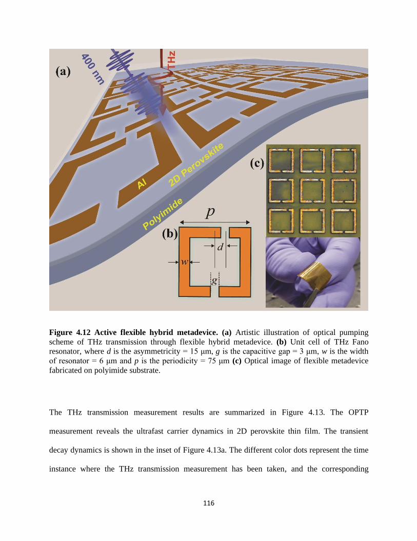
116
Figure 4.12 Active flexible hybrid metadevice. (a) Artistic illustration of optical pumping
scheme of THz transmission through flexible hybrid metadevice. (b) Unit cell of THz Fano
resonator, where d is the asymmetricity = 15 μm, g is the capacitive gap = 3 μm, w is the width
of resonator = 6 μm and p is the periodicity = 75 μm (c) Optical image of flexible metadevice
fabricated on polyimide substrate.
The THz transmission measurement results are summarized in Figure 4.13. The OPTP
measurement reveals the ultrafast carrier dynamics in 2D perovskite thin film. The transient
decay dynamics is shown in the inset of Figure 4.13a. The different color dots represent the time
instance where the THz transmission measurement has been taken, and the corresponding

117
transmission spectra are shown with their respective colors in Figure 4.13a. We used a
mechanical delay stage to introduce the time delay between pump and probe beam. Red dot
represents the time instance when the pump and probe beam are time matched thus the change in
THz transmission i.e. ∆T is maximum. At this instance, the density of charge carrier in
perovskite thin film are maximum thus manifesting as highly quenched Fano resonance
amplitude as shown by solid red line in Figure 4.13. The subsequent relaxation of free carriers
results in strengthening the Fano resonance as shown by yellow and green solid colors plots. The
complete retrieval of Fano resonance occur within 20 ps. Thus, changing the substrate does not
alter the performance of 2D perovskite coated hybrid metadevice in terms of its ultrafast
response. Further, we performed pump fluence dependent THz transmission measurement.
Increasing the pump fluence increases the number densities of charge carrier, thus Fano
resonance amplitude decrease. Figure 4.13b shows the pump fluence dependent THz
transmission. We observed complete modulation of Fano resonance at 350 µJ/cm2. As compared
to quartz substrate, the pump fluence number is slightly higher. It occurs may be due to the
difference in morphology of spin coated perovskite thin film on flexible substrate.

118
Figure 4.13 THz transmission through flexible metadevice (a) THz transmission for different
pump-probe delay time. The red solid line represents the maximum Fano resonance modulation
owing to maximum photoconductivity. The strength of Fano resonance is retrieved back as
farrier carriers are relax to equilibrium (green solid line). Inset shows the free carrier dynamics of
pristine 2D perovskite coated on polyimide substrate where dots represent the pump-probe time
instances where THz transmission measurements are taken. (b) Optical modulation of Fano
resonance. Complete quenching occurs for optical pump of fluence 350 µJ/cm2.
Further to show the robustness and flexibility of device performance, we performed the
transmission measurement by bending the flexible metadevice. Figure 4.14 shows the
experimentally measured THz transmission for bent metasurface. We observe THz modulation
for different bent metasurface. The detailed calculation of the curvature of metasurface is given
in Appendix A (section A3).

119
Figure 4.14 Curvature dependent THz transmission measurement (a, b and c) THz
transmission measurement from flexible device with radius of curvature (κ) 1.03, 0.84 and 0 cm-1
respectively.
4.5 References [1] A. Kojima, K. Teshima, Y. Shirai, T. Miyasaka, Journal of the American Chemical Society 2009,
131, 6050.
[2] J.-H. Im, C.-R. Lee, J.-W. Lee, S.-W. Park, N.-G. Park, Nanoscale 2011, 3, 4088. [3] M. M. Lee, J. Teuscher, T. Miyasaka, T. N. Murakami, H. J. Snaith, Science 2012, 338, 643.
[4] M. Liu, M. B. Johnston, H. J. Snaith, Nature 2013, 501, 395.
[5] L. M. Herz, Annual Review of Physical Chemistry 2016, 67, 65. [6] Y. Rong, L. Liu, A. Mei, X. Li, H. Han, Advanced Energy Materials 2015, 5, 1501066.
[7] Z. Wang, Z. Shi, T. Li, Y. Chen, W. Huang, Angewandte Chemie International Edition 2017, 56,
1190.
[8] H. Tsai, W. Nie, J.-C. Blancon, C. C. Stoumpos, R. Asadpour, B. Harutyunyan, A. J. Neukirch, R. Verduzco, J. J. Crochet, S. Tretiak, L. Pedesseau, J. Even, M. A. Alam, G. Gupta, J. Lou, P. M.
Ajayan, M. J. Bedzyk, M. G. Kanatzidis, A. D. Mohite, Nature 2016, 536, 312.
[9] Y. Chen, Y. Sun, J. Peng, J. Tang, K. Zheng, Z. Liang, Advanced Materials 2018, 30, 1703487. [10] M. Yuan, L. N. Quan, R. Comin, G. Walters, R. Sabatini, O. Voznyy, S. Hoogland, Y. Zhao, E.
M. Beauregard, P. Kanjanaboos, Z. Lu, D. H. Kim, E. H. Sargent, Nature Nanotechnology 2016, 11, 872.
[11] D. H. Cao, C. C. Stoumpos, O. K. Farha, J. T. Hupp, M. G. Kanatzidis, Journal of the American Chemical Society 2015, 137, 7843.
[12] L. Pedesseau, D. Sapori, B. Traore, R. Robles, H.-H. Fang, M. A. Loi, H. Tsai, W. Nie, J.-C.
Blancon, A. Neukirch, S. Tretiak, A. D. Mohite, C. Katan, J. Even, M. Kepenekian, ACS Nano 2016, 10,
9776. [13] I. C. Smith, E. T. Hoke, D. Solis-Ibarra, M. D. McGehee, H. I. Karunadasa, Angewandte Chemie
International Edition 2014, 53, 11232.
[14] X. Yang, X. Zhang, J. Deng, Z. Chu, Q. Jiang, J. Meng, P. Wang, L. Zhang, Z. Yin, J. You, Nature Communications 2018, 9, 570.
[15] R. L. Milot, R. J. Sutton, G. E. Eperon, A. A. Haghighirad, J. Martinez Hardigree, L. Miranda, H.
J. Snaith, M. B. Johnston, L. M. Herz, Nano Letters 2016, 16, 7001.
120
[16] G. Xing, B. Wu, X. Wu, M. Li, B. Du, Q. Wei, J. Guo, E. K. L. Yeow, T. C. Sum, W. Huang, Nature Communications 2017, 8, 14558.
[17] M. Tonouchi, Nature Photonics 2007, 1, 97.
[18] A. Y. Pawar, D. D. Sonawane, K. B. Erande, D. V. Derle, Drug Invention Today 2013, 5, 157.
[19] Applied Physics Letters 2006, 88, 153903. [20] T. Yasuda, T. Yasui, T. Araki, E. Abraham, Optics Communications 2006, 267, 128.
[21] Y. Liu, X. Zhang, Chemical Society Reviews 2011, 40, 2494.
[22] N. K. Grady, J. E. Heyes, D. R. Chowdhury, Y. Zeng, M. T. Reiten, A. K. Azad, A. J. Taylor, D. A. R. Dalvit, H.-T. Chen, Science 2013, 340, 1304.
[23] A. Minovich, J. Farnell, D. N. Neshev, I. McKerracher, F. Karouta, J. Tian, D. A. Powell, I. V.
Shadrivov, H. H. Tan, C. Jagadish, Y. S. Kivshar, Applied Physics Letters 2012, 100, 121113. [24] S. Savo, D. Shrekenhamer, W. J. Padilla, Advanced Optical Materials 2014, 2, 275.
[25] H.-T. Chen, W. J. Padilla, J. M. O. Zide, A. C. Gossard, A. J. Taylor, R. D. Averitt, Nature 2006,
444, 597.
[26] W. J. Padilla, A. J. Taylor, C. Highstrete, M. Lee, R. D. Averitt, Physical Review Letters 2006, 96, 107401.
[27] M. Manjappa, Y. K. Srivastava, L. Cong, I. Al-Naib, R. Singh, Advanced Materials 2017, 29,
1603355. [28] H. Tao, A. C. Strikwerda, K. Fan, W. J. Padilla, X. Zhang, R. D. Averitt, Physical Review Letters
2009, 103, 147401.
[29] Y. K. Srivastava, M. Manjappa, L. Cong, H. N. S. Krishnamoorthy, V. Savinov, P. Pitchappa, R. Singh, Advanced Materials 2018, 30, 1801257.
[30] S. H. Mousavi, I. Kholmanov, K. B. Alici, D. Purtseladze, N. Arju, K. Tatar, D. Y. Fozdar, J. W.
Suk, Y. Hao, A. B. Khanikaev, R. S. Ruoff, G. Shvets, Nano Letters 2013, 13, 1111.
[31] P. Pitchappa, M. Manjappa, C. P. Ho, R. Singh, N. Singh, C. Lee, Advanced Optical Materials 2016, 4, 541.
[32] Applied Physics Letters 2006, 88, 041109.
[33] B. Luk'yanchuk, N. I. Zheludev, S. A. Maier, N. J. Halas, P. Nordlander, H. Giessen, C. T. Chong, Nature Materials 2010, 9, 707.
[34] R. Singh, I. A. I. Al-Naib, M. Koch, W. Zhang, Opt. Express 2011, 19, 6312.
[35] R. Singh, I. Al-Naib, W. Cao, C. Rockstuhl, M. Koch, W. Zhang, IEEE Transactions on
Terahertz Science and Technology 2013, 3, 820. [36] D. Ghosh, D. Acharya, L. Pedesseau, C. Katan, J. Even, S. Tretiak, A. J. Neukirch, Journal of
Materials Chemistry A 2020, 8, 22009.
[37] J.-C. Blancon, H. Tsai, W. Nie, C. C. Stoumpos, L. Pedesseau, C. Katan, M. Kepenekian, C. M. M. Soe, K. Appavoo, M. Y. Sfeir, S. Tretiak, P. M. Ajayan, M. G. Kanatzidis, J. Even, J. J. Crochet, A.
D. Mohite, Science 2017, 355, 1288.
[38] F. Wang, J. Shan, M. A. Islam, I. P. Herman, M. Bonn, T. F. Heinz, Nature Materials 2006, 5, 861.
[39] C. He, L. Zhu, Q. Zhao, Y. Huang, Z. Yao, W. Du, Y. He, S. Zhang, X. Xu, Advanced Optical
Materials 2018, 6, 1800290.
[40] H. Shi, R. Yan, S. Bertolazzi, J. Brivio, B. Gao, A. Kis, D. Jena, H. G. Xing, L. Huang, ACS Nano 2013, 7, 1072.
[41] Z. Nie, R. Long, L. Sun, C.-C. Huang, J. Zhang, Q. Xiong, D. W. Hewak, Z. Shen, O. V.
Prezhdo, Z.-H. Loh, ACS Nano 2014, 8, 10931. [42] B. Gao, G. Hartland, T. Fang, M. Kelly, D. Jena, H. Xing, L. Huang, Nano Letters 2011, 11,
3184.
[43] D. Suzuki, S. Oda, Y. Kawano, Nature Photonics 2016, 10, 809. [44] X. Yang, A. Vorobiev, A. Generalov, M. A. Andersson, J. Stake, Applied Physics Letters 2017,
111, 021102.

121
[45] D. Simon, T. Ware, R. Marcotte, B. R. Lund, D. W. Smith, M. Di Prima, R. L. Rennaker, W.
Voit, Biomedical Microdevices 2013, 15, 925.
122
Chapter 5
Ultrafast THz photo physics of solvent
engineered triple-cation halide perovskite
5.1 Introduction
So far in the previous chapters, we have seen the positive performance of solution-processed
halide perovskite for ultrafast terahertz photonic devices. The performance of perovskite
integrated terahertz (THz) metadevice is highly depends on the free carrier dynamics of
perovskite. Thus, it is imperative to understand the mechanism of free carrier relaxation and the
factors that affect it. The theme of this chapter is to address this important question. In this
chapter, we investigate the nature of conduction and charge carrier dynamics of mixed organic-
inorganic cations [methylammonium (MA), formamidinium (FA) and cesium (Cs)] along with
mixed halides [iodine (I) and bromine (Br)] perovskite synthesized in different solvents using
optical pump terahertz probe (OPTP) spectroscopy. The reason for selecting mixed cation-anions
perovskite is its high ambience stability as compared to single cation-anion. Our studies reveal
that carrier mobilities, diffusion length and carrier relaxation dynamics strongly depend on the
type of solvent used for the preparation of the perovskite thin film. The mixed cation prepared
using dimethylforamide/dimethylsulfoxide (DMSO) solvent shows greater electronic properties
like mobility and diffusion length compared to γ-butyrolactone solvent. These findings provide
valuable insight to improve the charge carrier transport of perovskite thin film through solvent

123
engineering that not only is extremely useful for ultrafast THz photonic devices but also benefit
in improving the perovskite based solar cell performances.
5.2 Why mixed cation perovskite?
The emergence of hybrid organic-inorganic perovskite (HOIP) has revolutionize the field of
solar energy and optoelectronics application such as light emitting devices and lasing owing to
its excellent photoconversion efficiency and distinct optical features like high absorption and
tunable bandgap. However, one of the major challenges to realize the practical applications using
perovskite is its very low ambience instability particularly in the presence of moisture. To
mitigate this limitation engineering, the compositions of perovskites offer a positive route.
Substituting and mixing the various cations or anions or both offers a broad window for
performance optimization. In this regard, mixing the smaller inorganic cation, such as cesium
(Cs), has proven to be more effective in stabilizing the phase owing to its smaller size. Recently,
mixed organic-inorganic cations (methylammonium, formamidinium and cesium) along with the
mixed halides (iodine and bromine) [Cs0.05(MA0.17FA0.83)(0.95)Pb(I0.83Br0.17)3] have emerged as
promising candidate for solar cells with excellent photoconversion efficiency (~ 21 %)[1] and
better ambience stability.
5.3 Optical pump terahertz probe (OPTP) of mixed cation/anion
perovskite
To study the carrier dynamics and investigate we employed ZnTe based optical pump terahertz
probe spectroscopy where perovskite thin film was photoexcited using 400 nm pump beam and
the dynamics of excited carrier were probed using terahertz pulse. In the experiment, the
diameter of the optical pump and terahertz probe were kept 6 and 4 mm respectively, to ensure

124
the uniform excitation of the probe region. Terahertz radiation owing to its low photon energy (1
THz = 4.1 meV) is a perfect candidate to probe the free carrier dynamics in a non-contact way.
Additionally, the OPTP spectroscopy gives both the real and imaginary part of the complex
optical constants which allows to extract the carrier density, electronic mobility and diffusion
lengths.
We prepared the mixed cations (MA/FA/Cs) and anions (I/Br) using two different solutions
named as DMF/DMSO and GBL. Both the perovskite thin film spin coated on quartz substrate
for OPTP measurement. Photoexciting the perovskite thin film above the bandgap
instantaneously generate the free carrier that interacts with terahertz probe pulse, thereby
reducing the transmission. Thus, monitoring the change in terahertz transmission (∆T/T)
unravels the free carrier relaxation dynamics. We employed 400 nm as an optical pump beam
owing to energy (E ~ 3.1 eV) higher than the bandgap (Eg ~ 1.58 eV)[2] of perovskite thin film.
To unravel the carrier dynamics, we measured the change in transient photoconductivity of the
perovskite thin film as terahertz photoconductivity is directly proportional to the product of
charge carrier and carrier mobilities. Here, we assume that the carrier mobilities do not change
with pump-probe delay thus decay in terahertz transient reflects the temporal evolution of charge
carrier densities. To illustrate it more clearly, we write the mathematical expression of terahertz
photoconductivity using thin film approximation[3] as:
∆𝜎(𝑡𝑝) =
ɛ0𝑐
𝑑(𝑛𝑎𝑖𝑟 + 𝑛𝑠𝑢𝑏)
−∆𝑇(𝑡𝑝)
𝑇𝑁𝑜 𝑝𝑢𝑚𝑝 (5.1)
where, ∆T is the change in terahertz transmission, c is the velocity of light, TNo pump is the
terahertz transmission when the optical pump is absent, ɛ0 is the vacuum permittivity, 𝑛𝑎𝑖𝑟, 𝑛𝑠𝑢𝑏
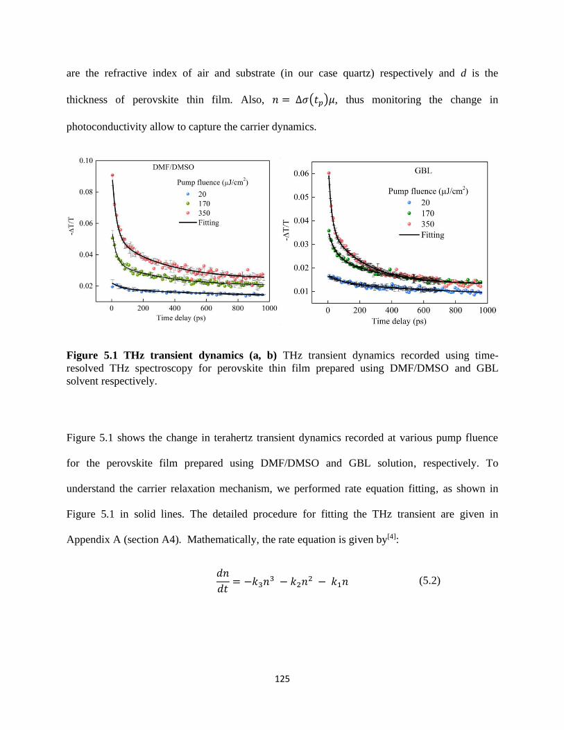
125
are the refractive index of air and substrate (in our case quartz) respectively and d is the
thickness of perovskite thin film. Also, 𝑛 = ∆𝜎(𝑡𝑝)𝜇, thus monitoring the change in
photoconductivity allow to capture the carrier dynamics.
Figure 5.1 THz transient dynamics (a, b) THz transient dynamics recorded using time-
resolved THz spectroscopy for perovskite thin film prepared using DMF/DMSO and GBL
solvent respectively.
Figure 5.1 shows the change in terahertz transient dynamics recorded at various pump fluence
for the perovskite film prepared using DMF/DMSO and GBL solution, respectively. To
understand the carrier relaxation mechanism, we performed rate equation fitting, as shown in
Figure 5.1 in solid lines. The detailed procedure for fitting the THz transient are given in
Appendix A (section A4). Mathematically, the rate equation is given by[4]:
𝑑𝑛
𝑑𝑡= −𝑘3𝑛
3 − 𝑘2𝑛2 − 𝑘1𝑛 (5.2)
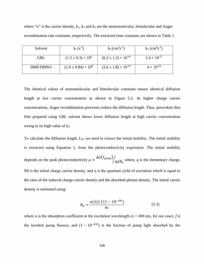
126
where “n” is the carrier density, k1, k2 and k3 are the monomolecular, bimolecular and Auger
recombination rate constants, respectively. The extracted time constants are shown in Table 1.
Solvent k1 (s-1) k2 (cm3s-1) k3 (cm6s-1)
GBL (1.5 ± 0.3) × 108 (6.2 ± 1.2) × 10-10 2.4 × 10⁻²⁷
DMF/DMSO (1.0 ± 0.84) × 108 (2.6 ± 1.8) × 10-10 4 × 10-28
The identical values of monomolecular and bimolecular constants ensure identical diffusion
length at low carrier concentration as shown in Figure 5.2. At higher charge carrier
concentrations, Auger recombination processes reduce the diffusion length. Thus, perovskite thin
film prepared using GBL solvent shows lower diffusion length at high carrier concentration
owing to its high value of k3.
To calculate the diffusion length, LD, we need to extract the initial mobility. The initial mobility
is extracted using Equation 1, from the photoconductivity expression. The initial mobility
depends on the peak photoconductivity 𝜇 =∆𝜎(𝑡𝑝𝑒𝑎𝑘)
𝑞𝜂𝑁0⁄ where, q is the elementary charge,
N0 is the initial charge carrier density, and η is the quantum yield of excitation which is equal to
the ratio of the induced charge-carrier density and the absorbed photon density. The initial carrier
density is estimated using:
𝑁0 =
𝛼(𝜆)𝜆 𝑓(1 − 10−𝑂𝐷)
ℎ𝑐 (5.3)
where α is the absorption coefficient at the excitation wavelength (λ = 400 nm, for our case), f is
the incident pump fluence, and (1 − 10−𝑂𝐷) is the fraction of pump light absorbed by the

127
sample, where OD is the optical density given by OD = 0.434 αl, where l is the thickness of
perovskite thin film.
Since the value of η lies between 0 and 1 (0 ≤ η ≤ 1), we extract the lower limit of charge-carrier
mobility using η = 1. The extracted mobilities at various pump fluences are shown in Figure 5.2.
The figure shows that the carrier mobilities for the perovskite thin film prepared using
DMF/DMSO (shown as solid red line) is high as compared to the thin film prepared using GBL
solvent (shown as solid black line). Also, by increasing the pump fluences, the mobilities
decrease from 300 to 80 cm2 (V s)-1 for the DMF/DMSO prepared film, while it decreases from
90 to 15 cm2 (V s)-1 for the GBL solvent. Both types of thin films exhibits the identical
decreasing trend with increasing pump fluence. We attribute this to increase in electron
scattering rate. At high pump fluences, the rise in free carrier densities leads to Auger
recombination which mainly involves many-body effects thus increases the scattering rate of free
carriers. The mathematical relation between mobility and scattering rate is following: 𝜇 = 𝑒 𝛤𝑚⁄ ,
where e, 𝛤, and m are the elementary charge, scattering rate and mass of free carrier respectively.
From the mathematical relation, it is clear that increasing scattering rates reduces the carrier
mobilities which is also evident in the experimentally extracted mobilities shown in Figure 5.2.
The solid red line represents the variation of carrier mobility as a function of pump fluence for
the perovskite film prepared using DMF/DMSO solvent, while the solid black line depicts the
mobilities for GBL prepared solvents. Figure 5.2 clearly shows that the film prepared using
DMF/DMSO solvent shows higher mobility compared to GBL solvent. This reflects the fact that
the morphology of film affects the electronic mobility.
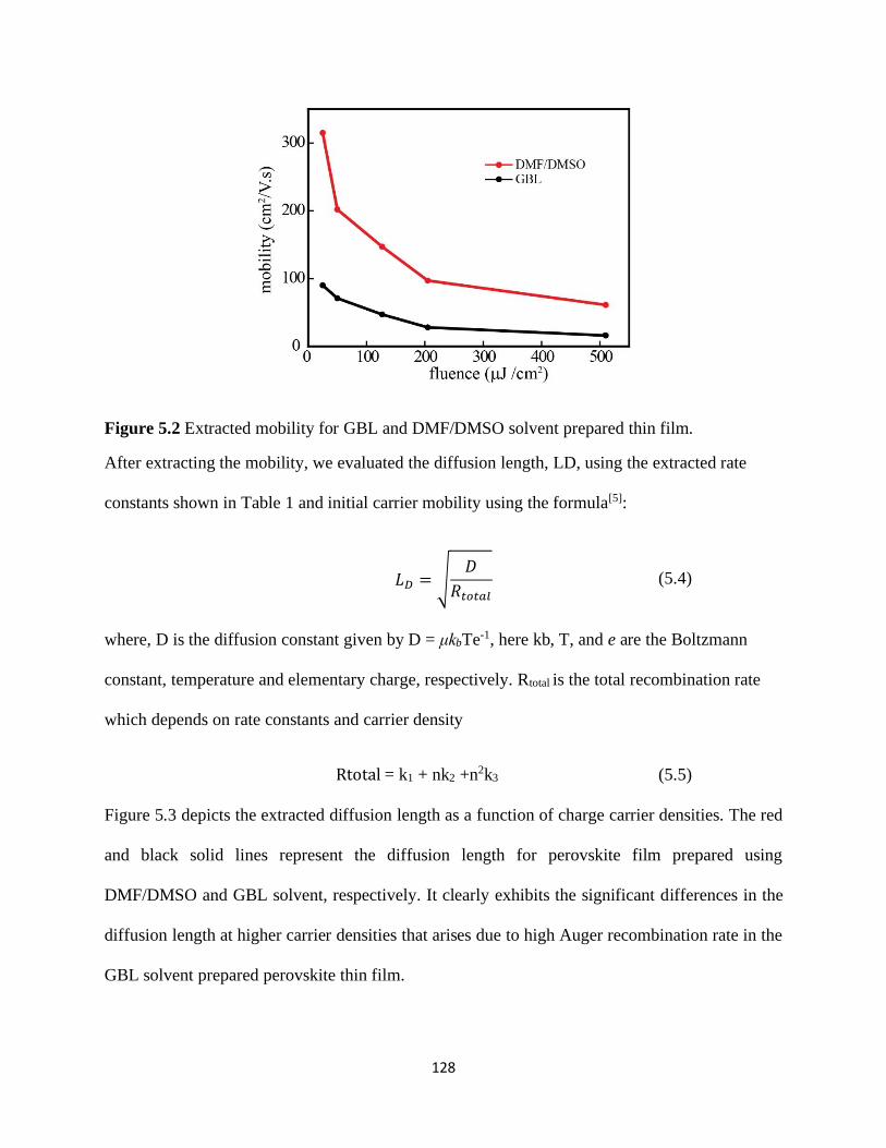
128
Figure 5.2 Extracted mobility for GBL and DMF/DMSO solvent prepared thin film.
After extracting the mobility, we evaluated the diffusion length, LD, using the extracted rate
constants shown in Table 1 and initial carrier mobility using the formula[5]:
𝐿𝐷 = √𝐷
𝑅𝑡𝑜𝑡𝑎𝑙 (5.4)
where, D is the diffusion constant given by D = μkbTe-1, here kb, T, and e are the Boltzmann
constant, temperature and elementary charge, respectively. Rtotal is the total recombination rate
which depends on rate constants and carrier density
Rtotal = k1 + nk2 +n2k3 (5.5)
Figure 5.3 depicts the extracted diffusion length as a function of charge carrier densities. The red
and black solid lines represent the diffusion length for perovskite film prepared using
DMF/DMSO and GBL solvent, respectively. It clearly exhibits the significant differences in the
diffusion length at higher carrier densities that arises due to high Auger recombination rate in the
GBL solvent prepared perovskite thin film.

129
Figure 5.3 Diffusion length calculated by THz spectroscopy reveals that the perovskite film
fabricated using DMF/DMSO solvent has high diffusion length.
The extracted mobilities and the diffusion length for the perovskite film prepared using
DMF/DMSO and GBL solutions exhibit significant differences. These differences can be
attributed to the difference in the film quality due to perovskite-solvent interaction. Figure 5.4
shows the morphology of the spin-coated perovskite thin films prepared using both the solvents.
Clearly, the morphology appears to be strongly dependent on the choice of the solvent. The SEM
images of the perovskite thin film prepared using DMF/DMSO (Figure 5.4a), and GBL (Figure
5.4b) solvents reveal that the film quality does depend on solvent. The DMF/DMSO solvent
prepared films have compact and bigger grain sizes, while GBL based solvent results in a
granular texture film. The slow crystallization in GBL solvent gives more defect dominated
films, that in turn restricts the mobility and the diffusion length.
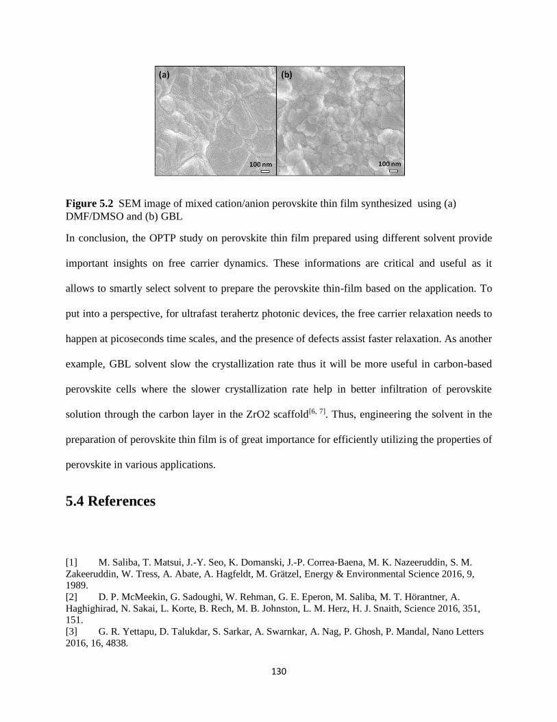
130
Figure 5.2 SEM image of mixed cation/anion perovskite thin film synthesized using (a)
DMF/DMSO and (b) GBL
In conclusion, the OPTP study on perovskite thin film prepared using different solvent provide
important insights on free carrier dynamics. These informations are critical and useful as it
allows to smartly select solvent to prepare the perovskite thin-film based on the application. To
put into a perspective, for ultrafast terahertz photonic devices, the free carrier relaxation needs to
happen at picoseconds time scales, and the presence of defects assist faster relaxation. As another
example, GBL solvent slow the crystallization rate thus it will be more useful in carbon-based
perovskite cells where the slower crystallization rate help in better infiltration of perovskite
solution through the carbon layer in the ZrO2 scaffold[6, 7]. Thus, engineering the solvent in the
preparation of perovskite thin film is of great importance for efficiently utilizing the properties of
perovskite in various applications.
5.4 References
[1] M. Saliba, T. Matsui, J.-Y. Seo, K. Domanski, J.-P. Correa-Baena, M. K. Nazeeruddin, S. M.
Zakeeruddin, W. Tress, A. Abate, A. Hagfeldt, M. Grätzel, Energy & Environmental Science 2016, 9, 1989.
[2] D. P. McMeekin, G. Sadoughi, W. Rehman, G. E. Eperon, M. Saliba, M. T. Hörantner, A.
Haghighirad, N. Sakai, L. Korte, B. Rech, M. B. Johnston, L. M. Herz, H. J. Snaith, Science 2016, 351, 151.
[3] G. R. Yettapu, D. Talukdar, S. Sarkar, A. Swarnkar, A. Nag, P. Ghosh, P. Mandal, Nano Letters
2016, 16, 4838.

131
[4] L. M. Herz, Annual Review of Physical Chemistry 2016, 67, 65. [5] C. Wehrenfennig, G. E. Eperon, M. B. Johnston, H. J. Snaith, L. M. Herz, Advanced Materials
2014, 26, 1584.
[6] A. Mei, X. Li, L. Liu, Z. Ku, T. Liu, Y. Rong, M. Xu, M. Hu, J. Chen, Y. Yang, M. Grätzel, H.
Han, Science 2014, 345, 295.
[7] J. Li, G. Niu, W. Li, K. Cao, M. Wang, L. Wang, Nanoscale 2016, 8, 14163.

132

133
Chapter 6
Conclusion and Future direction
With the advent of metamaterials (MMs), there has been rapid growth in terahertz (THz)
research activities. Over the year, MMs have offered exciting features and application in the field
of photonics. Their structural simplicity and ease to tune on-demand optical properties are the
major driving force that provided unprecedented control on electromagnetic waves (specifically
here THz waves).
The objective of this thesis was to develop ultrafast THz photonic devices based on solution
processed semiconductors (perovskite). A systematic study on the optical characterization of
perovskite thin films were presented to unravel the charge carrier dynamics. Followed by this,
the integration of MM with perovskite thin film on rigid as well as flexible substrate were
presented to demonstrate the ultrafast modulation of THz electric field. The works presented in
the thesis show a new prospect to develop a cost effective and efficient ultrafast THz device.
This will lay a platform for the new generation of MM based photonic devices in the THz region
and bridge the existing gap which is known as “THz-gap”.
Here we present the chapter wise conclusion: In chapter 1, we presented the general introduction
of THz waves, metamaterial and optical properties of the solution processed perovskite family. A
comparative study between conventional and halide perovskite semiconductor is presented to
showcase the potential of perovskite for new generation of ultrafast THz photonic devices.
In the first section of chapter 2, we discussed about the basics of numerical tools that have been
utilized to simulate the optical properties of MMs. Followed by this, a detailed section dedicated
134
to THz time domain spectroscopy (THz-TDS) is presented. It included both the photoconductive
antenna and nonlinear crystal (ZnTe) based THz TDS systems and their underlying working
mechanism. The experimental layout of Optical pump and terahertz probe (OPTP) is shown
which is the heart of this thesis. And the chapter is concluded with the fabrication details of
MMs.
Chapter 3,4 and 5 outline the different works of solution-processed perovskite-based hybrid MM
hybrid system. In chapter 3, we unravel the ultrafast free carrier dynamics in PbI2 thin film using
time-resolved THz spectroscopy. The integration of thin film of PbI2 with MM structures
enables near unity switching of Fano resonance at 150 ps time scale. Further, the interaction of
strongly confined THz electric field with PbI2 exhibit the change in carrier dynamics. This
finding is important as it provides a viable route to develop next-generation active metadevice
with multifunctionalities.
Chapter 4 includes the optical characterization of 2D perovskite where using for the first-time
using time resolved THz spectroscopy, we showed the dynamics of excitons. The results reveal
that the quantum well structure present in 2D perovskite act as an additional channel for the
photoexcited free carrier to relax back at ultrafast time scale which is fastest in the solution
processed perovskite semiconductor family. As an application outlook, we integrated the MM
with 2D perovskite in rigid as well flexible platform and experimentally demonstrated near unity
switching of Fano resonance at 20 ps time scales.
The chapter 5, discusses about the optical properties of perovskites prepared using a different
solvent. This study suggests that the optical properties of perovskites highly depends on the type
of solvent which being used during the fabrication process. These findings are important as it
135
provides an insight to smartly fabricate the perovskite based on the required optoelectronic
properties.
6.1 Future works
6.1.1 Active tuning of photon-phonon coupling
Strong light-matter interaction is the key enabler for numerous potential applications in various
branches of science such as chemistry, photonics, biosensing, nonlinear physics and many more.
Metamaterial offers a simple and tunable platform to confine on-demand terahertz (THz) electric
field inside a cavity. Thus, MMs can be an ideal platform to study the coupling of THz electric
field and matter resonance interactions. There are many materials whose lattice vibrations lie in
THz spectral region, thus integration of such materials with MM opens up new avenue to study
the light-matter interactions which are vital from fundamental as well as a technological point of
view.
In this prospect, interaction of THz electric field with halide perovskite is important as it offers a
potential way to tune the optoelectronic properties of perovskite. In general, the interaction
between light and matters are quantified based on the interaction strength and can be categorized
as strong and weak coupling. Both interactions regime is important and offers unique
phenomena, as an example, the weak coupling interaction of emitter with cavity alters the
spontaneous emission rate of emitter which is given by Purcell factors. Similarly, the strong
coupling regime is important to probe many fundamental phenomena and overcome the losses in
the coupled system. In this regard, the investigation of perovskite with a strongly confined THz

136
electric field facilitated by MMs is important. To start, we plan to couple the perovskite phonon
mode with MM resonance. The preliminary experimental results show that perovskite has
phonon modes which lie in the THz spectral region. Figure 6.1 shows the measured complex
conductivity of perovskite which suggest a phonon mode neat 1 THz associated with the bending
and stretching of the Pb-X (halide) bonds[1, 2]. Appearance of phonon modes in conductivity
spectra follows Lorentz behavior, where the real and imaginary parts are fitted simultaneously
using the standard Lorentz Oscillator model described in Eqn. 1
𝜎(𝜔) = −𝑖휀0ω(휀∞ − 1) + (휀0𝜔𝑝
2 𝜔
𝑖(𝜔0 2 −𝜔2) + 𝜔Г1
) (6.1)
where 𝜔𝑝, 𝜔0 and Г1 are plasma frequency, phonon resonance frequencies and the scattering rate
for the oscillator, respectively. The fitting parameters are show in Table 1 which confirms the
phonon resonance frequency at 1 THz.
Perovskite f0 (THz) 𝝎𝒑(THz) Г1 (THz) 𝜺∞
0.99 10.07 2.53 1
To investigate the coupling, we plan to integrate LC resonator with perovskite. The coupling of
strongly confined THz electric field in the capacitive gap of the LC resonator with phonon
resonance may lead to a strongly coupled system. That manifests as splitting in the transmission
spectra of perovskite integrated MM hybrid system. Further, the active tuning of coupling
strength via optical pumping is also an important aspect that we will investigate in this study.
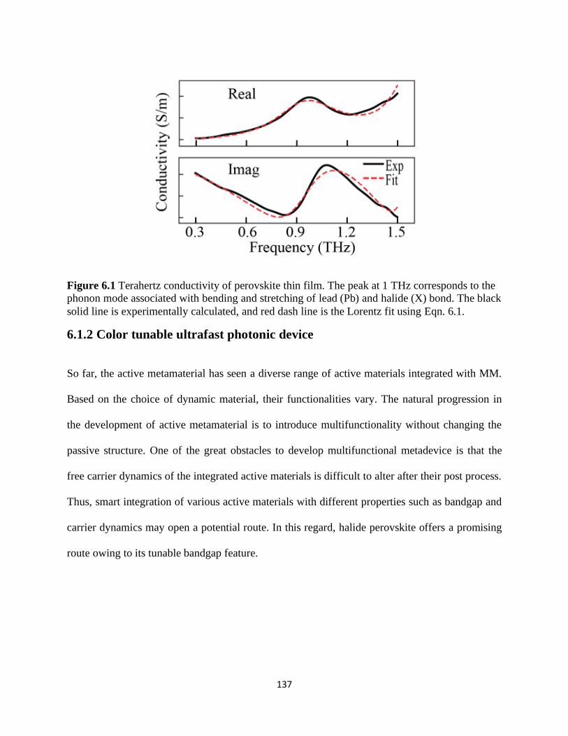
137
Figure 6.1 Terahertz conductivity of perovskite thin film. The peak at 1 THz corresponds to the
phonon mode associated with bending and stretching of lead (Pb) and halide (X) bond. The black
solid line is experimentally calculated, and red dash line is the Lorentz fit using Eqn. 6.1.
6.1.2 Color tunable ultrafast photonic device
So far, the active metamaterial has seen a diverse range of active materials integrated with MM.
Based on the choice of dynamic material, their functionalities vary. The natural progression in
the development of active metamaterial is to introduce multifunctionality without changing the
passive structure. One of the great obstacles to develop multifunctional metadevice is that the
free carrier dynamics of the integrated active materials is difficult to alter after their post process.
Thus, smart integration of various active materials with different properties such as bandgap and
carrier dynamics may open a potential route. In this regard, halide perovskite offers a promising
route owing to its tunable bandgap feature.
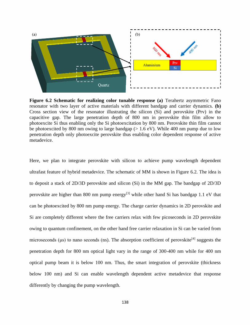
138
Figure 6.2 Schematic for realizing color tunable response (a) Terahertz asymmetric Fano
resonator with two layer of active materials with different bandgap and carrier dynamics. (b)
Cross section view of the resonator illustrating the silicon (Si) and perovskite (Prv) in the
capacitive gap. The large penetration depth of 800 nm in perovskite thin film allow to
photoexcite Si thus enabling only the Si photoexcitation by 800 nm. Perovskite thin film cannot
be photoexcited by 800 nm owing to large bandgap (> 1.6 eV). While 400 nm pump due to low
penetration depth only photoexcite perovskite thus enabling color dependent response of active
metadevice.
Here, we plan to integrate perovskite with silicon to achieve pump wavelength dependent
ultrafast feature of hybrid metadevice. The schematic of MM is shown in Figure 6.2. The idea is
to deposit a stack of 2D/3D perovskite and silicon (Si) in the MM gap. The bandgap of 2D/3D
perovskite are higher than 800 nm pump energy[3] while other hand Si has bandgap 1.1 eV that
can be photoexcited by 800 nm pump energy. The charge carrier dynamics in 2D perovskite and
Si are completely different where the free carriers relax with few picoseconds in 2D perovskite
owing to quantum confinement, on the other hand free carrier relaxation in Si can be varied from
microseconds (μs) to nano seconds (ns). The absorption coefficient of perovskite[4] suggests the
penetration depth for 800 nm optical light vary in the range of 300-400 nm while for 400 nm
optical pump beam it is below 100 nm. Thus, the smart integration of perovskite (thickness
below 100 nm) and Si can enable wavelength dependent active metadevice that response
differently by changing the pump wavelength.

139
Figure 6.3 (a) Absorption coefficient of methyl ammonium lead iodide perovskite to calculate
the wavelength dependent penetration depth[4]. (b) Penetration depth of perovskite for 800 and
400 nm are 400 nm and 50 nm calculated using l = 1/α, where α is the absorption coefficient of
perovskite shown in a.
6.2 References
[1] C. La-o-vorakiat, H. Xia, J. Kadro, T. Salim, D. Zhao, T. Ahmed, Y. M. Lam, J.-X. Zhu, R. A.
Marcus, M.-E. Michel-Beyerle, E. E. M. Chia, The Journal of Physical Chemistry Letters 2016, 7, 1. [2] F. Brivio, J. M. Frost, J. M. Skelton, A. J. Jackson, O. J. Weber, M. T. Weller, A. R. Goñi, A. M.
A. Leguy, P. R. F. Barnes, A. Walsh, Physical Review B 2015, 92, 144308.
[3] Z. Xiao, Y. Zhou, H. Hosono, T. Kamiya, N. P. Padture, Chemistry – A European Journal 2018, 24, 2305.
[4] Y. Li, W. Yan, Y. Li, S. Wang, W. Wang, Z. Bian, L. Xiao, Q. Gong, Scientific Reports 2015, 5,
14485.
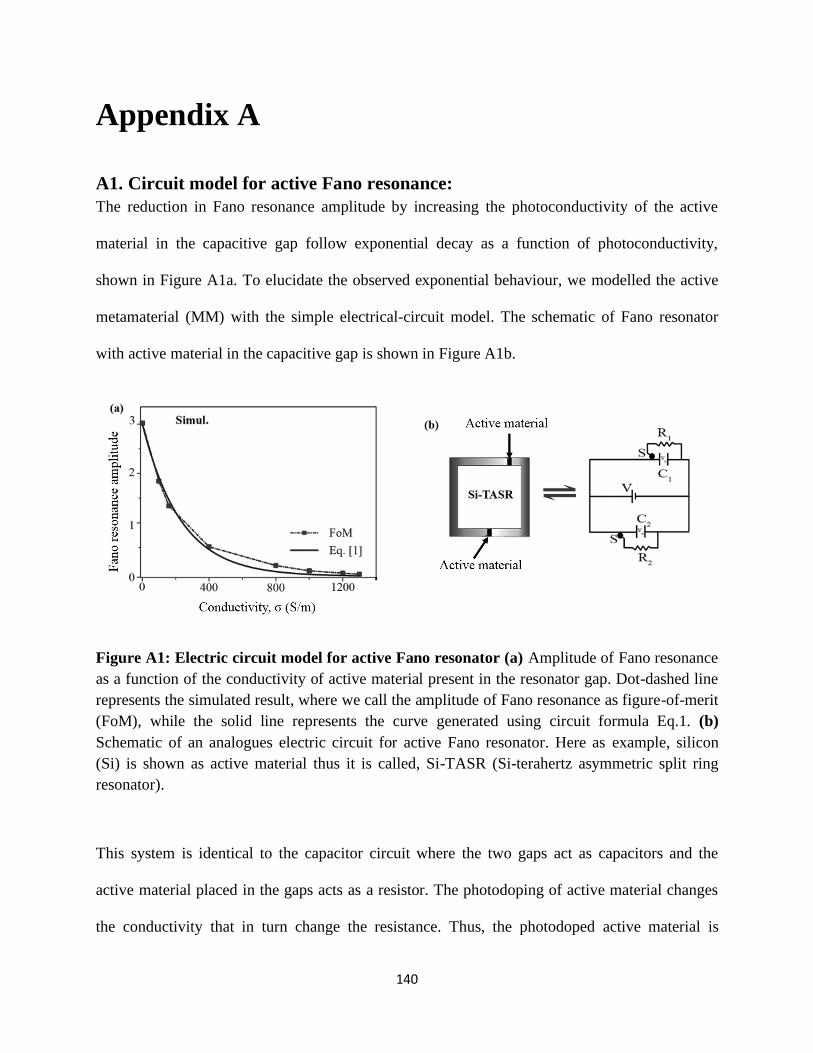
140
Appendix A
A1. Circuit model for active Fano resonance:
The reduction in Fano resonance amplitude by increasing the photoconductivity of the active
material in the capacitive gap follow exponential decay as a function of photoconductivity,
shown in Figure A1a. To elucidate the observed exponential behaviour, we modelled the active
metamaterial (MM) with the simple electrical-circuit model. The schematic of Fano resonator
with active material in the capacitive gap is shown in Figure A1b.
Figure A1: Electric circuit model for active Fano resonator (a) Amplitude of Fano resonance
as a function of the conductivity of active material present in the resonator gap. Dot-dashed line
represents the simulated result, where we call the amplitude of Fano resonance as figure-of-merit
(FoM), while the solid line represents the curve generated using circuit formula Eq.1. (b)
Schematic of an analogues electric circuit for active Fano resonator. Here as example, silicon
(Si) is shown as active material thus it is called, Si-TASR (Si-terahertz asymmetric split ring
resonator).
This system is identical to the capacitor circuit where the two gaps act as capacitors and the
active material placed in the gaps acts as a resistor. The photodoping of active material changes
the conductivity that in turn change the resistance. Thus, the photodoped active material is

141
modelled as a variable resistor. The equivalent circuit model is shown in Figure A1b. The
exponential decay of Fano resonance amplitude as a function of photoconductivity can be
understood by charge-discharge effect in the capacitor circuit. In the absence of an optical pump,
the incidence terahertz (THz) induces a circulating surface current and strong electric field
confinement in the gap as can be seen in Figure A1c. This induces a net capacitance in the
system. In the presence of the optical pump, the conductivity of active material that is present in
gap increases which gradually shorts the gap by increasing the photoconductivity. It results in a
reduction of electric field in the gap exponentially analogous to discharging of charge in RC
circuit. The relation between electric potential stored in Fano resonator gap and conductivity can
be given by:
𝑉𝑐 = 𝑉0𝑒−𝑅𝜎 (1)
here, 𝑉𝑐 is the stored electric potential, 𝑉0 is applied voltage, R0 is a constant which depends on
inversely proportional to the permittivity of active material present in gaps, and 𝜎 is the
conductivity of active material. Equation 1 is derived using the concept of discharging of the RC
circuit. The discharge in RC circuit is written by:
𝑉𝑐 = 𝑉0𝑒
−𝑡𝜏
(2)
where 𝜏 is the RC time constant equal to 𝜏 = 𝑅𝐶. Expressing the R in terms of conductivity σ
and using the expression of the parallel plate capacitor, the equation 2 can be rewritten as:
𝑉𝑐 = 𝑉0𝑒
−𝑡0𝐴1𝑔𝑙𝜀𝑟𝐴2
𝜎= 𝑉0𝑒
−𝑅𝜎 (3)
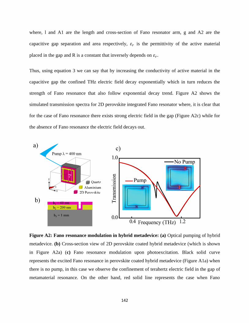
142
where, l and A1 are the length and cross-section of Fano resonator arm, g and A2 are the
capacitive gap separation and area respectively, 휀𝑟 is the permittivity of the active material
placed in the gap and R is a constant that inversely depends on 휀𝑟 .
Thus, using equation 3 we can say that by increasing the conductivity of active material in the
capacitive gap the confined THz electric field decay exponentially which in turn reduces the
strength of Fano resonance that also follow exponential decay trend. Figure A2 shows the
simulated transmission spectra for 2D perovskite integrated Fano resonator where, it is clear that
for the case of Fano resonance there exists strong electric field in the gap (Figure A2c) while for
the absence of Fano resonance the electric field decays out.
Figure A2: Fano resonance modulation in hybrid metadevice: (a) Optical pumping of hybrid
metadevice. (b) Cross-section view of 2D perovskite coated hybrid metadevice (which is shown
in Figure A2a) (c) Fano resonance modulation upon photoexcitation. Black solid curve
represents the excited Fano resonance in perovskite coated hybrid metadevice (Figure A1a) when
there is no pump, in this case we observe the confinement of terahertz electric field in the gap of
metamaterial resonance. On the other hand, red solid line represents the case when Fano
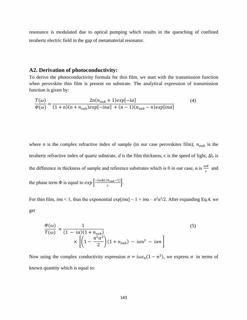
143
resonance is modulated due to optical pumping which results in the quenching of confined
terahertz electric field in the gap of metamaterial resonator.
A2. Derivation of photoconductivity:
To derive the photoconductivity formula for thin film, we start with the transmission function
when perovskite thin film is present on substrate. The analytical expression of transmission
function is given by:
𝑇(𝜔)
𝛷(𝜔)=
2n(𝑛𝑠𝑢𝑏 + 1)𝑒𝑥𝑝[−𝑖𝛼]
(1 + n)(n + 𝑛𝑠𝑢𝑏)𝑒𝑥𝑝[−𝑖𝑛𝛼] + (𝑛 − 1)(𝑛𝑠𝑢𝑏 − 𝑛)𝑒𝑥𝑝[𝑖𝑛𝛼]
(4)
where n is the complex refractive index of sample (in our case perovskites film), 𝑛𝑠𝑢𝑏 is the
terahertz refractive index of quartz substrate, d is the film thickness, c is the speed of light, ΔL is
the difference in thickness of sample and reference substrates which is 0 in our case, α is 𝜔𝑑
𝑐 and
the phase term Φ is equal to 𝑒𝑥𝑝 [−𝑖𝜔Δ𝐿(𝑛𝑠𝑢𝑏−1)
𝑐].
For thin film, inα < 1, thus the exponential exp[inα] ~ 1 + inα – n2α2/2. After expanding Eq.4. we
get
𝛷(𝜔)
𝑇(𝜔) ≈
1
(1 − 𝑖𝛼)(1 + 𝑛𝑠𝑢𝑏)
× [(1 − n2𝛼2
2) (1 + 𝑛𝑠𝑢𝑏) − 𝑖𝛼n
2 − 𝑖𝛼𝑛 ]
(5)
Now using the complex conductivity expression 𝜎 = 𝑖𝜔휀0(1 − 𝑛2), we express 𝜎 in terms of
known quantity which is equal to:
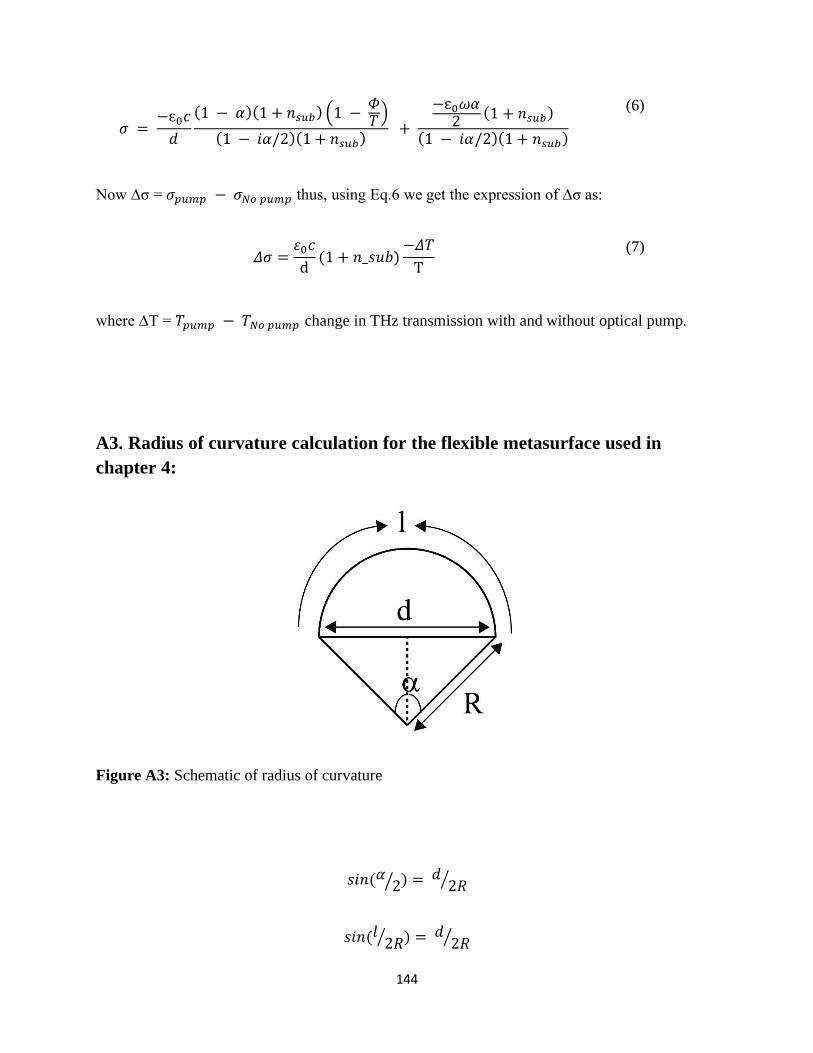
144
𝜎 = −ɛ0𝑐
𝑑
(1 − 𝛼)(1 + 𝑛𝑠𝑢𝑏) (1 − 𝛷𝑇)
(1 − 𝑖𝛼/2)(1 + 𝑛𝑠𝑢𝑏) +
−ɛ0𝜔𝛼2
(1 + 𝑛𝑠𝑢𝑏)
(1 − 𝑖𝛼/2)(1 + 𝑛𝑠𝑢𝑏)
(6)
Now ∆σ = 𝜎𝑝𝑢𝑚𝑝 − 𝜎𝑁𝑜 𝑝𝑢𝑚𝑝 thus, using Eq.6 we get the expression of ∆σ as:
𝛥𝜎 =
휀0𝑐
d(1 + 𝑛_𝑠𝑢𝑏)
−𝛥𝑇
T
(7)
where ∆T = 𝑇𝑝𝑢𝑚𝑝 − 𝑇𝑁𝑜 𝑝𝑢𝑚𝑝 change in THz transmission with and without optical pump.
A3. Radius of curvature calculation for the flexible metasurface used in
chapter 4:
Figure A3: Schematic of radius of curvature
𝑠𝑖𝑛(𝛼 2⁄ ) = 𝑑2𝑅⁄
𝑠𝑖𝑛(𝑙 2𝑅⁄ ) = 𝑑 2𝑅⁄
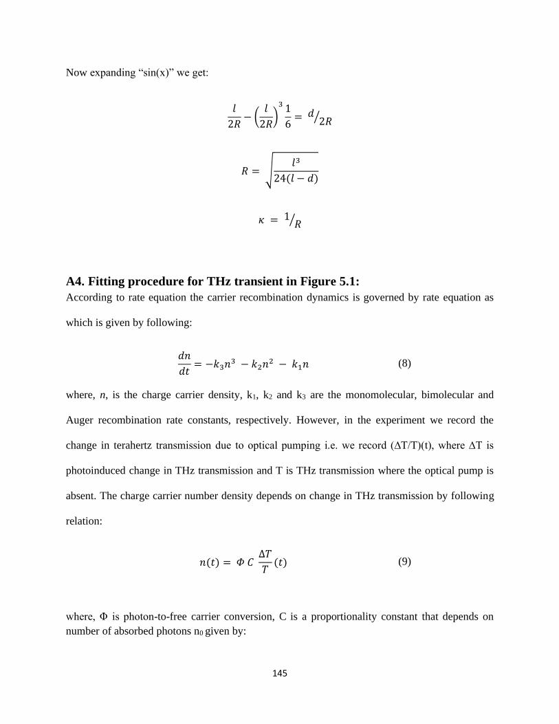
145
Now expanding “sin(x)” we get:
𝑙
2𝑅− (
𝑙
2𝑅)3 1
6= 𝑑 2𝑅⁄
𝑅 = √𝑙3
24(𝑙 − 𝑑)
𝜅 = 1 𝑅⁄
A4. Fitting procedure for THz transient in Figure 5.1:
According to rate equation the carrier recombination dynamics is governed by rate equation as
which is given by following:
𝑑𝑛
𝑑𝑡= −𝑘3𝑛
3 − 𝑘2𝑛2 − 𝑘1𝑛 (8)
where, n, is the charge carrier density, k1, k2 and k3 are the monomolecular, bimolecular and
Auger recombination rate constants, respectively. However, in the experiment we record the
change in terahertz transmission due to optical pumping i.e. we record (∆T/T)(t), where ∆T is
photoinduced change in THz transmission and T is THz transmission where the optical pump is
absent. The charge carrier number density depends on change in THz transmission by following
relation:
𝑛(𝑡) = 𝛷 𝐶
∆𝑇
𝑇(𝑡) (9)
where, Φ is photon-to-free carrier conversion, C is a proportionality constant that depends on
number of absorbed photons n0 given by:

146
𝑛0 =
𝛼(𝜆)𝜆 𝑓(1 − 10−𝑂𝐷)
ℎ𝑐 (10)
where α is the absorption coefficient at the excitation wavelength (λ = 400 nm, for our case), f is
the incident pump fluence, and (1 − 10−𝑂𝐷) is the fraction of pump light absorbed by the
sample, where OD is the optical density given by OD = 0.434 αl, where l is the thickness of
perovskite thin film.
Thus, substituting the expression of “n” in Eq.8. results in following:
𝑑𝑥
𝑑𝑡= −𝐶2𝛷2𝑘3𝑥
3 − 𝐶𝛷𝑘2𝑥2 − 𝑘1𝑛 (11)
where x = ∆𝑇
𝑇. Hence, we fit the Figure 5.1 (in main text, chapter 5) with Eq.11. that gives the
values of 𝛷2𝑘3, 𝛷𝑘2 and 𝑘1. Since the value of Φ is unknown, and its value lies between 0 < Φ <
1, thus we calculate the upper limit of rate constants.
A5. Carrier dynamics explanation:
The relaxation of photoexcited charge carrier follows various paths to relax back to the
equilibrium state. Figure A4 shows the schematic diagram that illustrates the recombination
mechanism for the photoexcited free carrier to relax back in semiconductor. Typically, the free
carrier follows trap-mediated, bimolecular recombination or many-body assisted Auger
recombination.
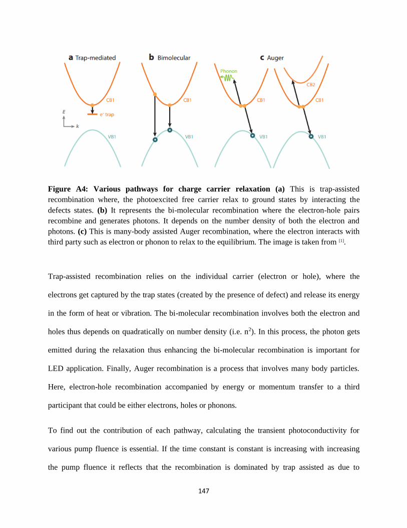
147
Figure A4: Various pathways for charge carrier relaxation (a) This is trap-assisted
recombination where, the photoexcited free carrier relax to ground states by interacting the
defects states. (b) It represents the bi-molecular recombination where the electron-hole pairs
recombine and generates photons. It depends on the number density of both the electron and
photons. (c) This is many-body assisted Auger recombination, where the electron interacts with
third party such as electron or phonon to relax to the equilibrium. The image is taken from [1].
Trap-assisted recombination relies on the individual carrier (electron or hole), where the
electrons get captured by the trap states (created by the presence of defect) and release its energy
in the form of heat or vibration. The bi-molecular recombination involves both the electron and
holes thus depends on quadratically on number density (i.e. n2). In this process, the photon gets
emitted during the relaxation thus enhancing the bi-molecular recombination is important for
LED application. Finally, Auger recombination is a process that involves many body particles.
Here, electron-hole recombination accompanied by energy or momentum transfer to a third
participant that could be either electrons, holes or phonons.
To find out the contribution of each pathway, calculating the transient photoconductivity for
various pump fluence is essential. If the time constant is constant is increasing with increasing
the pump fluence it reflects that the recombination is dominated by trap assisted as due to
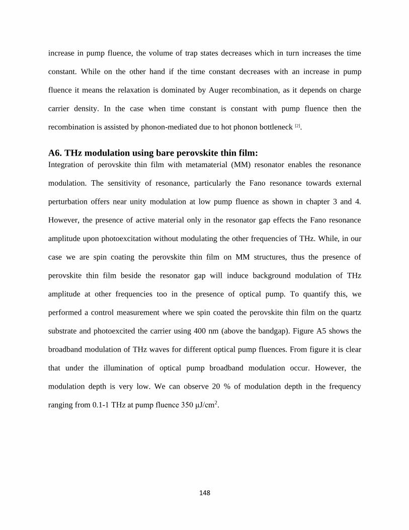
148
increase in pump fluence, the volume of trap states decreases which in turn increases the time
constant. While on the other hand if the time constant decreases with an increase in pump
fluence it means the relaxation is dominated by Auger recombination, as it depends on charge
carrier density. In the case when time constant is constant with pump fluence then the
recombination is assisted by phonon-mediated due to hot phonon bottleneck [2].
A6. THz modulation using bare perovskite thin film:
Integration of perovskite thin film with metamaterial (MM) resonator enables the resonance
modulation. The sensitivity of resonance, particularly the Fano resonance towards external
perturbation offers near unity modulation at low pump fluence as shown in chapter 3 and 4.
However, the presence of active material only in the resonator gap effects the Fano resonance
amplitude upon photoexcitation without modulating the other frequencies of THz. While, in our
case we are spin coating the perovskite thin film on MM structures, thus the presence of
perovskite thin film beside the resonator gap will induce background modulation of THz
amplitude at other frequencies too in the presence of optical pump. To quantify this, we
performed a control measurement where we spin coated the perovskite thin film on the quartz
substrate and photoexcited the carrier using 400 nm (above the bandgap). Figure A5 shows the
broadband modulation of THz waves for different optical pump fluences. From figure it is clear
that under the illumination of optical pump broadband modulation occur. However, the
modulation depth is very low. We can observe 20 % of modulation depth in the frequency
ranging from 0.1-1 THz at pump fluence 350 μJ/cm2.

149
Figure A5: Broadband modulation of THz using optical pumping of bare perovskite thin film.
A7. Effect of background modulation in THz Fano resonator:
In case of spin coating the perovskite thin film on MM resonator the remnant perovskite thin film
apart from resonator gap induces the background modulation of THz waves. However, there
exists contrasting difference between THz amplitude modulation at Fano resonance frequency
and other frequency where Fano resonance is not present. This is due to the highly sensitive
nature of Fano resonance towards external perturbation. Thus, Fano resonance switch off at very
low pump fluence which is low enough to induce contrasting difference in THz amplitude
modulation at other frequencies other than Fano resonance frequency. For example, in Figure
A5, we noticed that under the presence of an optical pump with pump fluence 350 μJ/cm2, there
is very low amplitude modulation. However, the presence of perovskite thin film on the top of
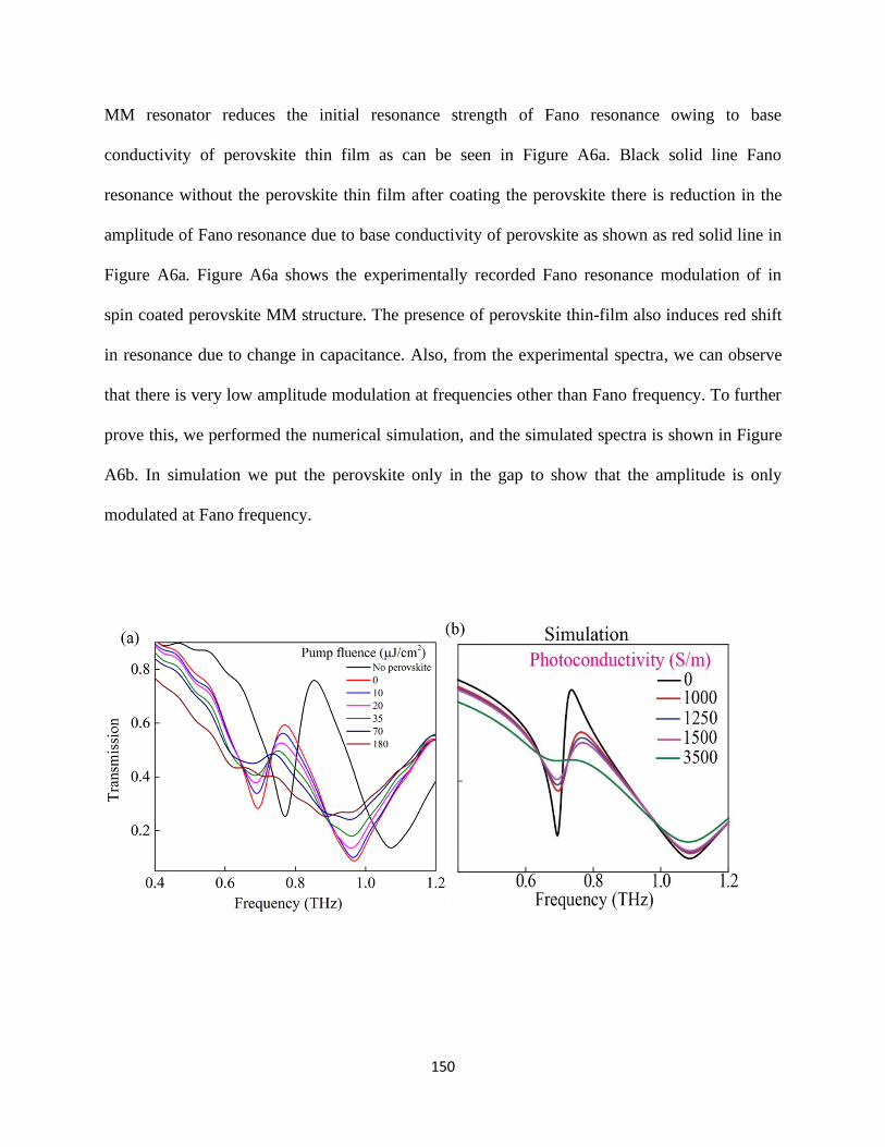
150
MM resonator reduces the initial resonance strength of Fano resonance owing to base
conductivity of perovskite thin film as can be seen in Figure A6a. Black solid line Fano
resonance without the perovskite thin film after coating the perovskite there is reduction in the
amplitude of Fano resonance due to base conductivity of perovskite as shown as red solid line in
Figure A6a. Figure A6a shows the experimentally recorded Fano resonance modulation of in
spin coated perovskite MM structure. The presence of perovskite thin-film also induces red shift
in resonance due to change in capacitance. Also, from the experimental spectra, we can observe
that there is very low amplitude modulation at frequencies other than Fano frequency. To further
prove this, we performed the numerical simulation, and the simulated spectra is shown in Figure
A6b. In simulation we put the perovskite only in the gap to show that the amplitude is only
modulated at Fano frequency.

151
Figure A6: Effect of eminent perovskite on Fano modulation (a) Experimentally recorded
transmission spectra for spin-coated perovskite on MM resonator (b) Simulated transmission
spectra for perovskite coated MM resonator system.
A7: AFM images of perovskite thin film
Figure A7: AFM images (a, b, c) AFM images of 2D, mixed 2D-3D and 3D perovskite
respectively.
References:
[1] L. M. Herz, Annual Review of Physical Chemistry 2016, 67, 65. [2] Z. Nie, R. Long, L. Sun, C.-C. Huang, J. Zhang, Q. Xiong, D. W. Hewak, Z. Shen, O. V.
Prezhdo, Z.-H. Loh, ACS Nano 2014, 8, 10931.

152
153
Copy Right/Reprint permission
Chapter 3 has been reproduced from the article “Solution-Processed Lead Iodide for Ultrafast
All-Optical Switching of Terahertz Photonic Devices”, Manu Manjappa, Ankur Solanki,
Abhishek Kumar, Tze Chien Sum, and Ranjan Singh, Advanced Materials, vol. 31, no. 32, p.
1901455, 2019. Copyright Wiley-VCH Verlag GmbH & Co. KGaA. Reproduced with
permission
Chapter 4 has been reproduced from the article “Excitons in 2D perovskites for ultrafast terahertz
photonic devices”, Abhishek Kumar, Ankur Solanki, Manukumara Manjappa, Sankaran
Ramesh, Yogesh Kumar Srivastava, Piyush Agarwal, Tze Chien Sum and R. Singh, Science
Advances, vol. 6, no. 8, p. eaax8821, 2020, From [Sci. Adv. 6, eaax8821 (2020)]. © The
Authors, some rights reserved; exclusive licensee American Association for the Advancement of
Science. Distributed under a Creative Commons Attribution NonCommercial License 4.0 (CC
BY-NC).
Chapter 5 has been reproduced from the article “Ultrafast THz photophysics of solvent
engineered triple-cation halide perovskites”, Abhishek Kumar, Anish Priyadarshi, Sudhanshu
Shukla, Manukumara Manjappa, Lew Jia Haur, Subodh G Mhaisalkar, Ranjan Singh, Reproduced
from [Journal of Applied Physics, vol. 124, no. 21, p. 215106, 2018, doi: 10.1063/1.5051561],
with the permission of AIP Publishing.
154
Appendix 1
Journal publications:
1. Abhishek Kumar, Ankur Solanki, Manukumara Manjappa, Sankaran Ramesh, Yogesh Kumar
Srivastava, Piyush Agarwal, Tze Chien Sum and R. Singh, "Excitons in 2D perovskites for
ultrafast terahertz photonic devices," Science Advances, vol. 6, no. 8, p. eaax8821, 2020, doi:
10.1126/sciadv. aax8821.
2. Abhishek Kumar, Anish Priyadarshi, Sudhanshu Shukla, Manukumara Manjappa, Lew Jia Haur,
Subodh G Mhaisalkar, Ranjan Singh, "Ultrafast THz photophysics of solvent engineered triple-
cation halide perovskites,” Journal of Applied Physics, vol. 124, no. 21, p. 215106, 2018, doi:
10.1063/1.5051561.
3. Abhishek Kumar, Yogesh Kumar Srivastava, Manukumara Manjappa, and Ranjan Singh,
“Color-Sensitive Ultrafast Optical Modulation and Switching of Terahertz Plasmonic Devices,"
Advanced Optical Materials, vol. 6, no. 15, p. 1800030, 2018, doi: 10.1002/adom.201800030.
4. Prakash Pitchappa, Abhishek Kumar, Haidong Liang, Saurav Prakash, Nan Wang, Andrew A
Bettiol, Thirumalai Venkatesan, Chengkuo Lee, Ranjan Singh, "Frequency-Agile Temporal Terahertz Metamaterials," Advanced Optical Materials, doi: 10.1002/adom.202000101.
5. Prakash Pitchappa, Abhishek Kumar, Saurav Prakash, Hariom Jani, Thirumalai Venkatesan, and
Ranjan Singh, "Chalcogenide Phase Change Material for Active Terahertz Photonics," Advanced
Materials, vol. 31, no. 12, p. 1808157, 2019, doi: 10.1002/adma.201808157.
6. Manu Manjappa, Ankur Solanki, Abhishek Kumar, Tze Chien Sum, and Ranjan Singh,
"Solution-Processed Lead Iodide for Ultrafast All-Optical Switching of Terahertz Photonic
Devices," Advanced Materials, vol. 31, no. 32, p. 1901455, 2019, doi:
10.1002/adma.201901455.
7. Song Han, Longqing Cong, Yogesh Kumar Srivastava, Bo Qiang, Mikhail V Rybin, Abhishek
Kumar, Ravi Jain, Wen Xiang Lim, Venu Gopal Achanta, Shriganesh S Prabhu, Qi Jie Wang,
Yuri S Kivshar, Ranjan Singh, "All-Dielectric Active Terahertz Photonics Driven by Bound
States in the Continuum," Advanced Materials, vol. 31, no. 37, p. 1901921, 2019, doi:
10.1002/adma.201901921.
8. Wen Xiang Lim, Manukumara Manjappa, Yogesh Kumar Srivastava, Longqing Cong, Abhishek
Kumar, Kevin F MacDonald, Ranjan Singh, “Ultrafast All-Optical Switching of Germanium-
Based Flexible Metaphotonic Devices," Advanced Materials, vol. 30, no. 9, p. 1705331,
2018, doi: 10.1002/adma.201705331.
9. Yogesh Kumar Srivastava, Apoorva Chaturvedi, Manukumara Manjappa, Abhishek Kumar,
Govind Dayal, Christian Kloc, Ranjan Singh, “MoS2 for Ultrafast All-Optical Switching and
Modulation of THz Fano Metaphotonic Devices," Advanced Optical Materials, vol. 5, no.
23, p. 1700762, 2017, doi: 10.1002/adom.201700762.
10. Manukumara Manjappa, Yogesh Kumar Srivastava, Ankur Solanki, Abhishek Kumar, Tze
Chien Sum, and Ranjan Singh, "Hybrid Lead Halide Perovskites for Ultrasensitive
Photoactive Switching in Terahertz Metamaterial Devices,” Advanced Materials, vol. 29,
no. 32, p. 1605881, 2017, doi: 10.1002/adma.201605881.