ultrafast carrier dynamics in microcrystalline silicon ...lts.fzu.cz/pdfpub/09-prb.pdf · ultrafast...
TRANSCRIPT
Ultrafast carrier dynamics in microcrystalline silicon probed by time-resolvedterahertz spectroscopy
L. Fekete, P. Kužel,* H. Němec, F. Kadlec, A. Dejneka, J. Stuchlík, and A. FejfarInstitute of Physics, Academy of Sciences of the Czech Republic, Na Slovance 2, 182 21 Prague 8, Czech Republic
Received 24 November 2008; revised manuscript received 27 January 2009; published 10 March 2009
We present the results of optical-pump–terahertz probe experiments applied to a set of thin-film microcrys-talline silicon samples, with structures varying from amorphous to fully microcrystalline. The samples wereexcited at wavelengths 800 and 400 nm and studied at temperatures down to 20 K. The character of nanoscopicelectrical transport properties markedly change on a subpicosecond time scale. The initial transient photocon-ductivity of the samples is dominated by hot free carriers with a mobility of 70 cm2 /Vs. These carriers arerapidly within 0.6 ps trapped into weakly localized hopping states. The hopping process dominates theterahertz spectra on the picosecond and subnanosecond time scales. The saturated high-frequency value of thehopping mobility is limited by the sample disorder in the amorphous sample and by electron-phonon interac-tion for microcrystalline samples.
DOI: 10.1103/PhysRevB.79.115306 PACS numbers: 72.20.i, 78.47.jc, 73.50.h
I. INTRODUCTION
Hydrogenated microcrystalline silicon c-Si:H is a ma-terial with a wide range of potential applications not only inthe solar cell industry, but also in the technology of activematrices of displays and other optoelectronic elements.1 As itcombines the advantages of crystalline silicon c-Si, cur-rently the most important material for electronic applica-tions, with those of low-cost thin-film technology, it has be-come very attractive for large-area applications. Thec-Si:H has a complicated heterogeneous microstructure,which consists of a mixture of crystalline silicon grains,grain boundaries, voids, and amorphous silicon “tissue.”Samples with different structure and therefore different elec-tronic transport properties such as the lifetime and mobilityof charge carriers can be prepared by tuning the depositionparameters. The lifetime and the mobility of the carriers onpicosecond and nanosecond timescales are significantly in-fluenced by the material structure degree of crystallinity,grain arrangements, and sizes.
The methods classically used to investigate the photocon-ductivity of the samples, namely, transient photocurrentspectroscopy TPC and time-of-flight TOF spectros-copy,2,3 are able to characterize the carrier transport overmacroscopic distances drift mobility with a time resolutionof about 10 ns or lower. However, the samples have to haveohmic contacts TPC or p-i-n structure TOF. In contrast,the time-resolved terahertz spectroscopy4,5 is a contact-freemethod able to follow the local 110−7 m in-plane mo-tion of charges with a subpicosecond to nanosecond timeresolution. With this time resolution it is possible to investi-gate the carrier transport within the nanostructural compo-nents and the different conductivity mechanisms may thenappear simultaneously as different fingerprints in the time-resolved terahertz spectra Drude-like conductivity, hopping,etc.5,6 The investigation of the electronic hopping processesin disordered semiconductors in the terahertz range is of par-ticular interest as this range may overlap with the frequencyregion where the hopping mechanism saturates and the re-lated conductivity reaches its maximum. This regime is sel-dom observed in other experiments.
In this contribution we report on optical pump-terahertzprobe OPTP experiments with a series of thin microcrys-talline silicon c-Si:H layers with different crystallinity.Preliminary results on these samples were presented in Ref. 6with the following correspondence in the notation a-C0=Ca; C20=Cm1; C47=Cm2; C72=Cm3. Here we ap-ply two different excitation wavelengths 400 and 800 nmallowing us to probe the films to different depths. In addition,measurements at various temperatures 20, 100, 150, 300 Kprovide a way to identify the origin of the observed localizedstates.
II. EXPERIMENTAL PART
A. Samples
We studied one fully amorphous Ca and three c-Sisamples Cm1, Cm2, Cm3 prepared by plasma enhancedchemical vapor deposition 70 Pa; 250 °C; other depositionparameters are summarized in Table I. The hydrogen/silanedilution was adjusted to obtain samples with a different de-gree of crystallinity. The samples were deposited on
1102-oriented 1050.5 mm3 sapphire substrates andtheir thickness was measured by a surface profilometer Ten-cor AlphaStep.
The surface of the samples was investigated by ambientair Veeco atomic force microscope Dimension 3100, yield-ing an average grain size and rms roughness of the samples
TABLE I. Deposition parameters and surface characteristics ofsamples; rms stands for the rms roughness of the surface.
Samplecode
Thicknessnm
RF powerW H2 /SiH4
Grain sizenm
rms
nm
Ca 89050 9.5 12.8 5
Cm1 92050 9.5 23.8 720100 70
Cm2 77050 9.5 29.4 47050 22
Cm3 77050 9.7 47.6 28050 10
PHYSICAL REVIEW B 79, 115306 2009
1098-0121/2009/7911/11530613 ©2009 The American Physical Society115306-1
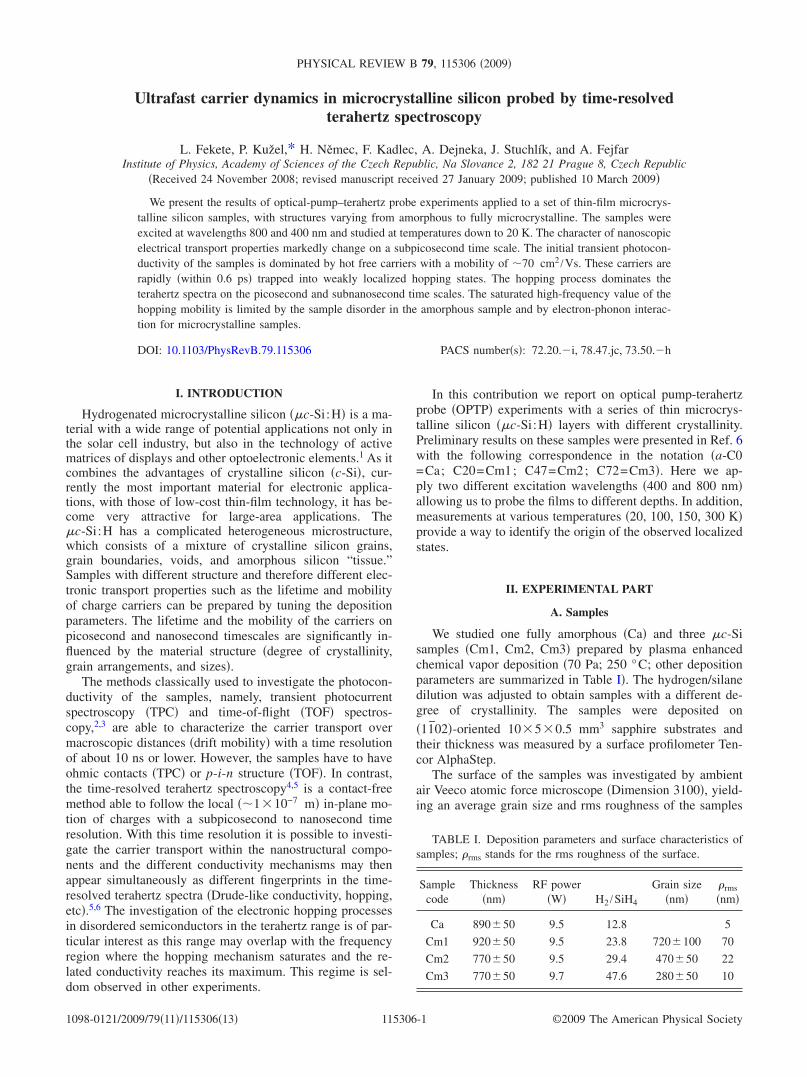
Table I. The growth itself starts from isolated Si microcrys-tals from an amorphous incubation layer. The microcrystalsare approximately spherically capped conical structures,7,8
but once they collide during their growth, they create bound-aries which are almost straight. The boundaries divide thesample area into natural neighboring areas available for thegrowth of each grain and this kind of growth can be modeledas a Voronoi tessellation.9 As the grains are sphericallycapped, the increasing rms roughness is a measure of theincreasing grain size see Fig. 1.
B. Raman spectroscopy
Exact evaluation of the crystallinity in microcrystallinesilicon is rather complicated10,11 because of its complexstructure. Consequently, several different methods for the de-composition of Raman spectra, leading to different values ofcrystallinity, can be found in the literature.12–14 In our case,the crystallinity Table II was obtained from the decompo-sition of the Raman spectra into areas of amorphous andmicrocrystalline grain contributions,14 taking into accountthe ratio of back-scattering cross sections of the phases.15
Several different excitation wavelengths were used: 442nm He-Cd laser, 514 nm Ar+laser, 633 nm He-Ne la-ser, and 785 nm semiconductor diode laser. Since the lightpenetration depth decreases with increasing excitation wave-length, we could analyze the crystallinity from differentdepths of the samples.
Probing with 785 and 633 nm wavelength yields informa-tion about the average thin-film crystallinity nominal pen-etration depths for the crystalline Si are 10 and 1.5 m,respectively. In contrast, the penetration depths for excita-tion at 514 nm 0.25 m and 442 nm 40 nm are smaller
than the thickness of the samples and the crystallinity eithernear the front or near the back side of the thin film illumi-nated then through the sapphire substrate is obtained. Ana-logically, the entire film or only its surface are probed in theOPTP experiments with 800 and 400 nm excitation, respec-tively.
C. Spectroscopic ellipsometry
A quantitative evaluation of OPTP experiments requiresthe knowledge of initial concentration of photoexcited carri-ers, which is directly linked to the absorption coefficient ofthin films. For this purpose, the optical properties of the fullyamorphous and of the most crystalline samples labeled Caand Cm3, respectively were studied using spectroscopic el-lipsometry. Ellipsometric measurements were performedwith a J. A. Woollam spectral ellipsometer working in therotating analyzer mode at the incidence angle of 70°. A spe-cially designed ultrahigh vacuum UHV cryostat system al-lowed the low-temperature measurements of ellipsometricangles and at various wavelengths and at temperaturesdown to 20 K.
The spectral measurements were performed in the wave-length range from 350 to 1000 nm. It is well known that theabsorption coefficients of Si at the wavelengths of interest,400 and 800 nm, differ by about three orders of magnitude;furthermore, the layers exhibit a complex vertical micro-structure on a scale comparable with the wavelength. Forthese reasons, the task to set up a layered model appropriatefor the whole spectral range would be too complex. Instead,we have calculated effective optical constants separately inthe intervals 375–425 and 775–825 nm, assuming a singlehomogeneous layer on an infinite substrate. The experimen-tal data were analyzed with the software package WVASE32.The best agreement of our model with the experimental re-sults was achieved for the values of surface roughness from15 to 30 nm, which is consistent with the atomic force mi-croscopy results. While this approximative approach doesnot guarantee a high precision of the values of the absorptioncoefficient, it is a reliable way of determining its relativechanges with temperature, needed for the evaluation ofOPTP experiments. The results are summarized in Table III.We stress that these results correctly reflect the temperaturedependence of the absorption coefficient for our samples. Inthe cases when the absolute values at room temperature are
FIG. 1. Scheme of the crystalline grain growth in the amorphousmatrix.
TABLE II. Raman crystallinity of the samples in %; illumination from the front side FS and from theback side BS.
Samplecode
Excitation wavelength
442 nm 514 nm 633 nm 785 nm
FS BS FS BS FS BS FS BS
Ca 0 0 0 0 0 0 0 0
Cm1 62 0 57 0 20 19 23 23
Cm2 75 3 73 67 52 53 58 58
Cm3 80 47 75 70 70 70 73 73
FEKETE et al. PHYSICAL REVIEW B 79, 115306 2009
115306-2
expected to play an important role, data from Ref. 16 areconsidered instead.
D. Time-resolved terahertz spectroscopy
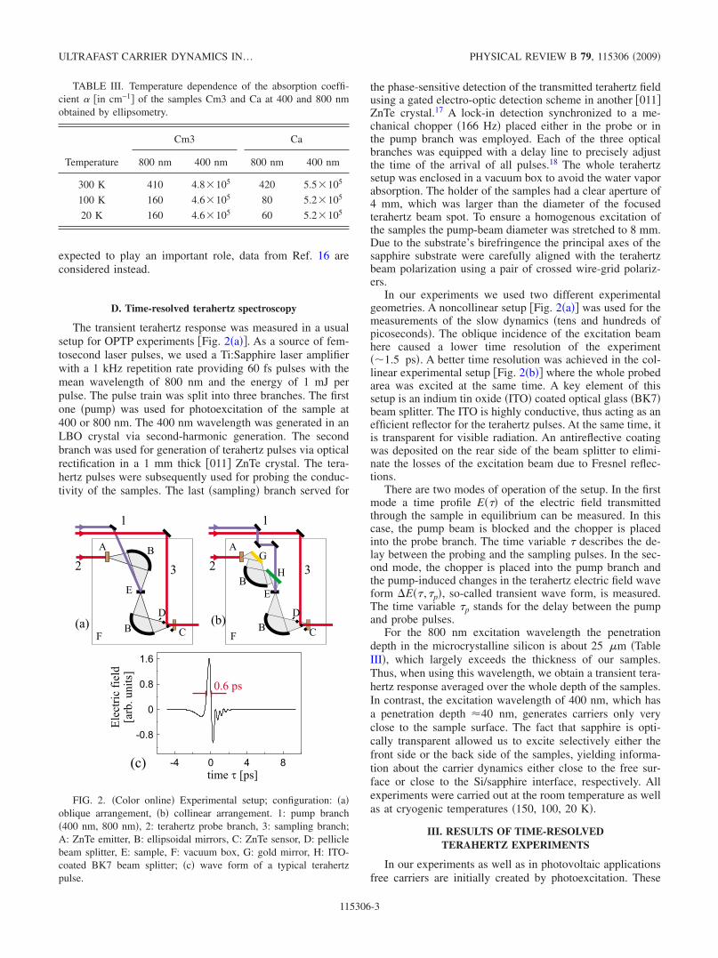
The transient terahertz response was measured in a usualsetup for OPTP experiments Fig. 2a. As a source of fem-tosecond laser pulses, we used a Ti:Sapphire laser amplifierwith a 1 kHz repetition rate providing 60 fs pulses with themean wavelength of 800 nm and the energy of 1 mJ perpulse. The pulse train was split into three branches. The firstone pump was used for photoexcitation of the sample at400 or 800 nm. The 400 nm wavelength was generated in anLBO crystal via second-harmonic generation. The secondbranch was used for generation of terahertz pulses via opticalrectification in a 1 mm thick 011 ZnTe crystal. The tera-hertz pulses were subsequently used for probing the conduc-tivity of the samples. The last sampling branch served for
the phase-sensitive detection of the transmitted terahertz fieldusing a gated electro-optic detection scheme in another 011ZnTe crystal.17 A lock-in detection synchronized to a me-chanical chopper 166 Hz placed either in the probe or inthe pump branch was employed. Each of the three opticalbranches was equipped with a delay line to precisely adjustthe time of the arrival of all pulses.18 The whole terahertzsetup was enclosed in a vacuum box to avoid the water vaporabsorption. The holder of the samples had a clear aperture of4 mm, which was larger than the diameter of the focusedterahertz beam spot. To ensure a homogenous excitation ofthe samples the pump-beam diameter was stretched to 8 mm.Due to the substrate’s birefringence the principal axes of thesapphire substrate were carefully aligned with the terahertzbeam polarization using a pair of crossed wire-grid polariz-ers.
In our experiments we used two different experimentalgeometries. A noncollinear setup Fig. 2a was used for themeasurements of the slow dynamics tens and hundreds ofpicoseconds. The oblique incidence of the excitation beamhere caused a lower time resolution of the experiment1.5 ps. A better time resolution was achieved in the col-linear experimental setup Fig. 2b where the whole probedarea was excited at the same time. A key element of thissetup is an indium tin oxide ITO coated optical glass BK7beam splitter. The ITO is highly conductive, thus acting as anefficient reflector for the terahertz pulses. At the same time, itis transparent for visible radiation. An antireflective coatingwas deposited on the rear side of the beam splitter to elimi-nate the losses of the excitation beam due to Fresnel reflec-tions.
There are two modes of operation of the setup. In the firstmode a time profile E of the electric field transmittedthrough the sample in equilibrium can be measured. In thiscase, the pump beam is blocked and the chopper is placedinto the probe branch. The time variable describes the de-lay between the probing and the sampling pulses. In the sec-ond mode, the chopper is placed into the pump branch andthe pump-induced changes in the terahertz electric field waveform E ,p, so-called transient wave form, is measured.The time variable p stands for the delay between the pumpand probe pulses.
For the 800 nm excitation wavelength the penetrationdepth in the microcrystalline silicon is about 25 m TableIII, which largely exceeds the thickness of our samples.Thus, when using this wavelength, we obtain a transient tera-hertz response averaged over the whole depth of the samples.In contrast, the excitation wavelength of 400 nm, which hasa penetration depth 40 nm, generates carriers only veryclose to the sample surface. The fact that sapphire is opti-cally transparent allowed us to excite selectively either thefront side or the back side of the samples, yielding informa-tion about the carrier dynamics either close to the free sur-face or close to the Si/sapphire interface, respectively. Allexperiments were carried out at the room temperature as wellas at cryogenic temperatures 150, 100, 20 K.
III. RESULTS OF TIME-RESOLVEDTERAHERTZ EXPERIMENTS
In our experiments as well as in photovoltaic applicationsfree carriers are initially created by photoexcitation. These
TABLE III. Temperature dependence of the absorption coeffi-cient in cm−1 of the samples Cm3 and Ca at 400 and 800 nmobtained by ellipsometry.
Temperature
Cm3 Ca
800 nm 400 nm 800 nm 400 nm
300 K 410 4.8105 420 5.5105
100 K 160 4.6105 80 5.2105
20 K 160 4.6105 60 5.2105
FIG. 2. Color online Experimental setup; configuration: aoblique arrangement, b collinear arrangement. 1: pump branch400 nm, 800 nm, 2: terahertz probe branch, 3: sampling branch;A: ZnTe emitter, B: ellipsoidal mirrors, C: ZnTe sensor, D: pelliclebeam splitter, E: sample, F: vacuum box, G: gold mirror, H: ITO-coated BK7 beam splitter; c wave form of a typical terahertzpulse.
ULTRAFAST CARRIER DYNAMICS IN… PHYSICAL REVIEW B 79, 115306 2009
115306-3
carriers can be characterized by a delocalized wave function.Their interaction with terahertz radiation is typically verystrong due to their high mobility. By contrast, if the carriersare captured in deep or shallow traps or if they are localizedat grain boundaries by potential barriers, their motion can bedescribed by a localized wave function and the carriers canbe detected in terahertz experiments only if their resonantfrequency lies near the terahertz range or if they remain mo-bile. These different types of behavior represent several con-tributions in the terahertz response with quite different spec-tral and temporal characteristics.
A. Pump-probe scans
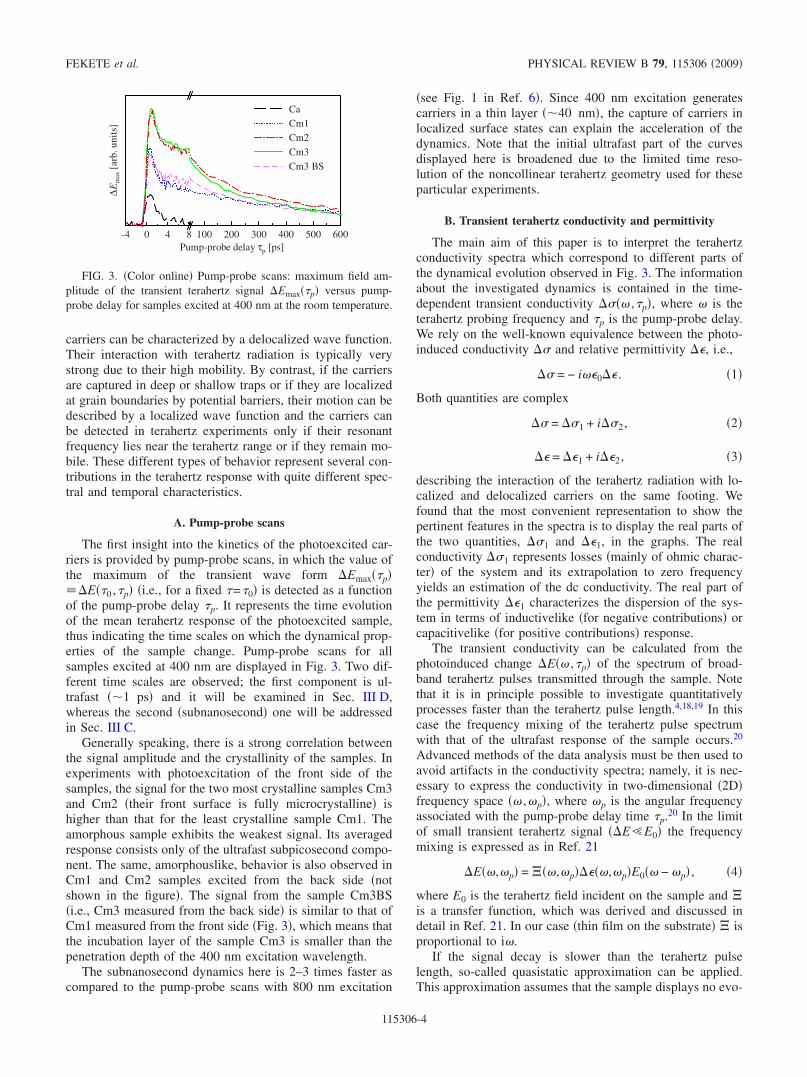
The first insight into the kinetics of the photoexcited car-riers is provided by pump-probe scans, in which the value ofthe maximum of the transient wave form EmaxpE0 ,p i.e., for a fixed =0 is detected as a functionof the pump-probe delay p. It represents the time evolutionof the mean terahertz response of the photoexcited sample,thus indicating the time scales on which the dynamical prop-erties of the sample change. Pump-probe scans for allsamples excited at 400 nm are displayed in Fig. 3. Two dif-ferent time scales are observed; the first component is ul-trafast 1 ps and it will be examined in Sec. III D,whereas the second subnanosecond one will be addressedin Sec. III C.
Generally speaking, there is a strong correlation betweenthe signal amplitude and the crystallinity of the samples. Inexperiments with photoexcitation of the front side of thesamples, the signal for the two most crystalline samples Cm3and Cm2 their front surface is fully microcrystalline ishigher than that for the least crystalline sample Cm1. Theamorphous sample exhibits the weakest signal. Its averagedresponse consists only of the ultrafast subpicosecond compo-nent. The same, amorphouslike, behavior is also observed inCm1 and Cm2 samples excited from the back side notshown in the figure. The signal from the sample Cm3BSi.e., Cm3 measured from the back side is similar to that ofCm1 measured from the front side Fig. 3, which means thatthe incubation layer of the sample Cm3 is smaller than thepenetration depth of the 400 nm excitation wavelength.
The subnanosecond dynamics here is 2–3 times faster ascompared to the pump-probe scans with 800 nm excitation
see Fig. 1 in Ref. 6. Since 400 nm excitation generatescarriers in a thin layer 40 nm, the capture of carriers inlocalized surface states can explain the acceleration of thedynamics. Note that the initial ultrafast part of the curvesdisplayed here is broadened due to the limited time reso-lution of the noncollinear terahertz geometry used for theseparticular experiments.
B. Transient terahertz conductivity and permittivity
The main aim of this paper is to interpret the terahertzconductivity spectra which correspond to different parts ofthe dynamical evolution observed in Fig. 3. The informationabout the investigated dynamics is contained in the time-dependent transient conductivity ,p, where is theterahertz probing frequency and p is the pump-probe delay.We rely on the well-known equivalence between the photo-induced conductivity and relative permittivity , i.e.,
= − i0 . 1
Both quantities are complex
= 1 + i2, 2
= 1 + i2, 3
describing the interaction of the terahertz radiation with lo-calized and delocalized carriers on the same footing. Wefound that the most convenient representation to show thepertinent features in the spectra is to display the real parts ofthe two quantities, 1 and 1, in the graphs. The realconductivity 1 represents losses mainly of ohmic charac-ter of the system and its extrapolation to zero frequencyyields an estimation of the dc conductivity. The real part ofthe permittivity 1 characterizes the dispersion of the sys-tem in terms of inductivelike for negative contributions orcapacitivelike for positive contributions response.
The transient conductivity can be calculated from thephotoinduced change E ,p of the spectrum of broad-band terahertz pulses transmitted through the sample. Notethat it is in principle possible to investigate quantitativelyprocesses faster than the terahertz pulse length.4,18,19 In thiscase the frequency mixing of the terahertz pulse spectrumwith that of the ultrafast response of the sample occurs.20
Advanced methods of the data analysis must be then used toavoid artifacts in the conductivity spectra; namely, it is nec-essary to express the conductivity in two-dimensional 2Dfrequency space ,p, where p is the angular frequencyassociated with the pump-probe delay time p.20 In the limitof small transient terahertz signal E E0 the frequencymixing is expressed as in Ref. 21
E,p = ,p,pE0 − p , 4
where E0 is the terahertz field incident on the sample and is a transfer function, which was derived and discussed indetail in Ref. 21. In our case thin film on the substrate isproportional to i.
If the signal decay is slower than the terahertz pulselength, so-called quasistatic approximation can be applied.This approximation assumes that the sample displays no evo-
100 200 300 400 500 600Pump-probe delay τp [ps]
-4 0 4 8
∆Em
ax[a
rb.u
nits
]CaCm1Cm2
Cm3Cm3 BS
FIG. 3. Color online Pump-probe scans: maximum field am-plitude of the transient terahertz signal Emaxp versus pump-probe delay for samples excited at 400 nm at the room temperature.
FEKETE et al. PHYSICAL REVIEW B 79, 115306 2009
115306-4
lution of its state during the probing event 1–2 ps, cf.Fig. 2c. In other words, all the relevant dynamics are con-nected to small p compared to the terahertz frequenciesp and the frequency mixing in Eq. 4 can be ne-glected,
E,p = ,0,pE0 , 5
or in the time p domain
E,p = ,0,pE0 . 6
C. Subnanosecond dynamics
1. Model
We first study the spectra related to the subnanosecondpart using the above described quasistatic approximation.The transient conductivity ,p is then extracted fromEqs. 6 and 1,
,p =− i0E,p
ErefT
,0, 7
where T is the equilibrium transmission spectrum of thesample and Eref is a reference wave form transmittedthrough the sample with the pump-beam blocked.
Generally, the dynamical response in the quasistatic ap-proximation can be written in the factorized form
,p = ei
ginip , 8
where the sum is made over the individual contributions tothe terahertz response; gi describes the spectral responsei.e., frequency-dependent mobility of the ith componentand nip corresponds to its carrier density decay.
In our previous paper6 we analyzed the room-temperaturedata within a model comprising a Drude term and relaxationterms. The Drude model accounts for delocalized carriers,
gD;D =e
m
1
1/D − i= D
1
1 − iD, 9
where D is the momentum scattering time of the carriers;D=De /m is the dc limit of their microscopic mobility andm is their effective mass. Note that D scales the amplitudeof the conductivity and determines its spectrum. An impor-tant characteristic of this model is that the real part of thepermittivity is negative 10 and that the dc conductivityis nonzero. In contrast, the response of localized carrierscase of hopping or localization within a well is frequentlydescribed by an overdamped oscillator or Debye relaxator.22
In the case of a Debye term with the relaxation frequency1 /R one gets
gR;R = R− i
1/R − i. 10
Carriers in this case feel a restoring force and, as a conse-quence, they do not contribute to the dc conductivity. Theconductivity increases with frequency and in the high-frequency regime R1 it saturates; the coefficient R
then can be understood as a saturated high-frequency mobil-ity.
In the case of the hopping conductivity more complexmodels should be used; their particular form reflects the un-derlying hopping mechanism. Here we used the model pro-posed by Dyre23
gH = iH1 −lnmin/max
ln1 − imin − ln1 − imax
lnmax/min
1/min − 1/max, 11
where 1 /max and 1 /min are low and high cutoff frequencies,respectively, which roughly delimit the range of the conduc-tivity dispersion. This model has qualitatively similar fea-tures to the Debye relaxator; however, it permits to describethe dispersion of the conductivity due to the hopping overseveral frequency decades as well as dc conduction.23 Notethat in real physical situations a drop of the conductivity dueto the inertia of carriers must always occur above somethreshold in the high-frequency regime. This is not taken intoaccount either in Debye or in the above hopping model.However, our experimental data show that the dynamics weobserve does not enter this regime.
2. Results and interpretation
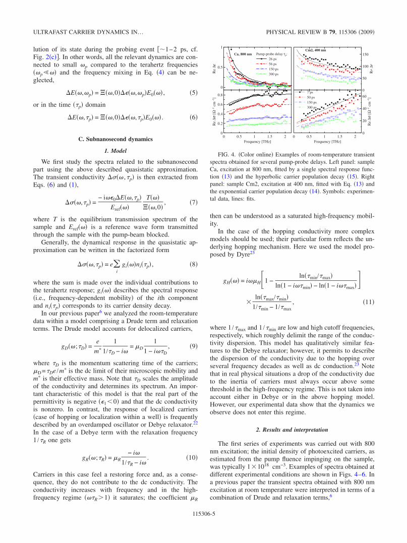
The first series of experiments was carried out with 800nm excitation; the initial density of photoexcited carriers, asestimated from the pump fluence impinging on the sample,was typically 11018 cm−3. Examples of spectra obtained atdifferent experimental conditions are shown in Figs. 4–6. Ina previous paper the transient spectra obtained with 800 nmexcitation at room temperature were interpreted in terms of acombination of Drude and relaxation terms,6
0.5 1 1.5 2
1
0.5
0
Re
∆ε
0 0.5 1 1.5 2Frequency [THz]
0.8
0.6
0.4
0.2
0
Re
∆σ[Ω
-1cm
-1]
Pump-probe delay τp:26 ps56 ps
150 ps300 ps
Ca, 800 nm
0.5 1 1.5 2
150
100
50
0
Re
∆ε
0 0.5 1 1.5 2Frequency [THz]
60
40
20
0
Re
∆σ[Ω
-1cm
-1]
7 ps
50 ps150 ps300 ps
Cm2, 400 nm
FIG. 4. Color online Examples of room-temperature transientspectra obtained for several pump-probe delays. Left panel: sampleCa, excitation at 800 nm, fitted by a single spectral response func-tion 13 and the hyperbolic carrier population decay 15. Rightpanel: sample Cm2, excitation at 400 nm, fitted with Eq. 13 andthe exponential carrier population decay 14. Symbols: experimen-tal data, lines: fits.
ULTRAFAST CARRIER DYNAMICS IN… PHYSICAL REVIEW B 79, 115306 2009
115306-5
,p/e = gDnDp + gR,slownR,slowp
+ gR,fastnR,fastp . 12
However, further investigation presented in the current paperhas revealed that the expected temperature dependence of thepertinent model parameters within this interpretation wouldcontradict the experimental data. These issues will be ad-dressed in the discussion.
We think that the observed spectra can be understoodwithin a hypothesis of a dominant hopping carrier transport,i.e., without a significant Drude-like contribution of the car-riers. We assume that the activation of the hopping process
occurs at frequencies much below the terahertz range1 /max 1 THz. Also our experimental data show that theconductivity drops with decreasing frequency in the subtera-hertz range and does not show any leveling off. In this re-gime Eq. 11 can be replaced by
gH = 0 − iHmin ln1 + i/min , 13
where the static mobility 0 accounts for some conductivityprocess occurring below the accessible terahertz spectralrange. This contribution is very small for all microcrystallinesamples and our data do not allow discussing its origin. Thesubnanosecond charge transport in both microcrystalline andamorphous samples can be thus described by a single for-mula. The essential difference in the behavior of the samplesconsists in very different values of min and H.
The same kind of fitting was performed for the data ob-tained with 400 nm excitation see Figs. 4–6. Here the ini-tial density of carriers is of about 51019 cm−3 and thisexplains the experimentally obtained higher values of theconductivity than for excitation at 800 nm. However, thenumber of carriers interacting with the terahertz wave issmaller than for the 800 nm excitation due to a much shorterabsorption length. As a consequence the transient terahertzsignal obtained with 400 nm pump is weaker and the corre-sponding conductivity data appear more noisy.
We found that the evolution of the carrier density n ofmicrocrystalline samples can be well described by a singleexponential decay with time constant H,
nHp = nH0e−p/H. 14
For the amorphous sample, the carrier density displays a hy-perbolic decay as previously observed also by optical pump-probe spectroscopy24,
nHp =nH0
1 + p/H. 15
An important quantity directly accessible from experimentaldata is the initial transient conductivity defined as
H = eHnH0 . 16
For each sample and each temperature transient spectra atseveral pump-probe delays were acquired 5–6 spectra for800 nm excitation wavelength and 4–7 spectra for 400 nmexcitation wavelength. The spectra for all measured pump-probe delays were fitted simultaneously in one global fit byEq. 8 with a single spectral response function describinghopping process 13 and with a single function describingthe population decay. Each curve presented in the figures is aresult of this global fit for a particular pump-probe delay. Forone sample and pump wavelength at a given temperature wethus have four fitting parameters 0, H, H, min to de-scribe 4–7 complex spectra. The quality of these fits can bechecked in Fig. 4 for both excitation wavelengths. Note thatwe used the complex conductivity data in the fits; in thisrepresentation the low-frequency part of the spectrum has asmaller weight than in the permittivity plots. This is at the
0.5 1 1.5 2
20
10
0
Re
∆ε
0.5 1 1.5 2
0
-5
-10
Im∆σ
[Ω-1
cm-1
]
0 0.5 1 1.5 2Frequency [THz]
12
8
4
0
Re
∆σ[Ω
-1cm
-1]
800 nm
Cm2
Cm3Cm1Ca
0.5 1 1.5 2
120
80
40
Re
∆ε
0.5 1 1.5 2Frequency [THz]
0
-20
-40
-60
-80
Im∆σ
[Ω-1
cm-1
]
0 0.5 1 1.5 2Frequency [THz]
60
40
20
0
Re
∆σ[Ω
-1cm
-1]
400 nm
Cm3BS
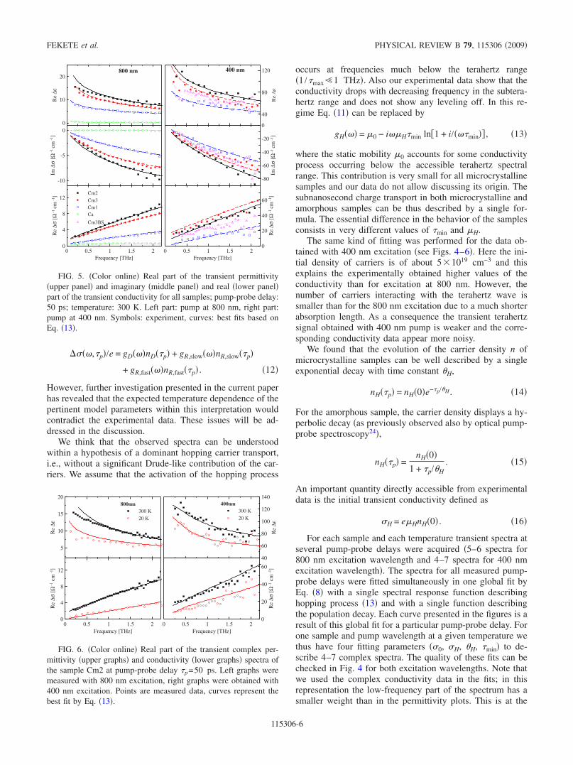
FIG. 5. Color online Real part of the transient permittivityupper panel and imaginary middle panel and real lower panelpart of the transient conductivity for all samples; pump-probe delay:50 ps; temperature: 300 K. Left part: pump at 800 nm, right part:pump at 400 nm. Symbols: experiment, curves: best fits based onEq. 13.
0.5 1 1.5 2
20
15
10
5
Re
∆ε
0 0.5 1 1.5 2Frequency [THz]
12
8
4
0
Re
∆σ[Ω
-1cm
-1]
0.5 1 1.5 2
140
120
100
80
60
40
Re
∆ε
400nm300 K
20 K
0 0.5 1 1.5 2Frequency [THz]
60
40
20
0
Re
∆σ[Ω
-1cm
-1]
800nm300 K
20 K
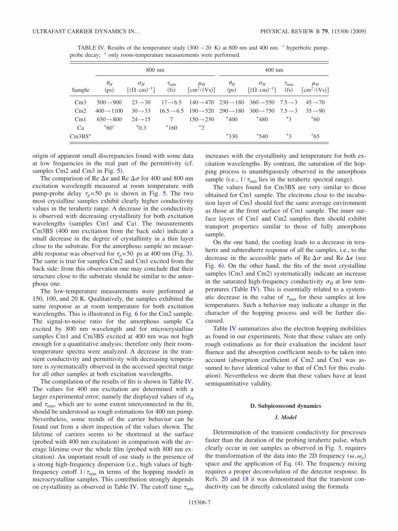
FIG. 6. Color online Real part of the transient complex per-mittivity upper graphs and conductivity lower graphs spectra ofthe sample Cm2 at pump-probe delay p=50 ps. Left graphs weremeasured with 800 nm excitation, right graphs were obtained with400 nm excitation. Points are measured data, curves represent thebest fit by Eq. 13.
FEKETE et al. PHYSICAL REVIEW B 79, 115306 2009
115306-6
origin of apparent small discrepancies found with some dataat low frequencies in the real part of the permittivity cf.samples Cm2 and Cm3 in Fig. 5.
The comparison of Re and Re for 400 and 800 nmexcitation wavelength measured at room temperature withpump-probe delay p=50 ps is shown in Fig. 5. The twomost crystalline samples exhibit clearly higher conductivityvalues in the terahertz range. A decrease in the conductivityis observed with decreasing crystallinity for both excitationwavelengths samples Cm1 and Ca. The measurementsCm3BS 400 nm excitation from the back side indicate asmall decrease in the degree of crystallinity in a thin layerclose to the substrate. For the amorphous sample no measur-able response was observed for p=50 ps at 400 nm Fig. 3.The same is true for samples Cm2 and Cm1 excited from theback side: from this observation one may conclude that theirstructure close to the substrate should be similar to the amor-phous one.
The low-temperature measurements were performed at150, 100, and 20 K. Qualitatively, the samples exhibited thesame response as at room temperature for both excitationwavelengths. This is illustrated in Fig. 6 for the Cm2 sample.The signal-to-noise ratio for the amorphous sample Caexcited by 800 nm wavelength and for microcrystallinesamples Cm1 and Cm3BS excited at 400 nm was not highenough for a quantitative analysis; therefore only their room-temperature spectra were analyzed. A decrease in the tran-sient conductivity and permittivity with decreasing tempera-ture is systematically observed in the accessed spectral rangefor all other samples at both excitation wavelengths.
The compilation of the results of fits is shown in Table IV.The values for 400 nm excitation are determined with alarger experimental error; namely the displayed values of Hand min, which are to some extent interconnected in the fit,should be understood as rough estimations for 400 nm pump.Nevertheless, some trends of the carrier behavior can befound out from a short inspection of the values shown. Thelifetime of carriers seems to be shortened at the surfaceprobed with 400 nm excitation in comparison with the av-erage lifetime over the whole film probed with 800 nm ex-citation. An important result of our study is the presence ofa strong high-frequency dispersion i.e., high values of high-frequency cutoff 1 /min in terms of the hopping model inmicrocrystalline samples. This contribution strongly dependson crystallinity as observed in Table IV. The cutoff time min
increases with the crystallinity and temperature for both ex-citation wavelengths. By contrast, the saturation of the hop-ping process is unambiguously observed in the amorphoussample i.e., 1 /min lies in the terahertz spectral range.
The values found for Cm3BS are very similar to thoseobtained for Cm1 sample. The electrons close to the incuba-tion layer of Cm3 should feel the same average environmentas those at the front surface of Cm1 sample. The inner sur-face layers of Cm1 and Cm2 samples then should exhibittransport properties similar to those of fully amorphoussample.
On the one hand, the cooling leads to a decrease in tera-hertz and subterahertz response of all the samples, i.e., to thedecrease in the accessible parts of Re and Re seeFig. 6. On the other hand, the fits of the most crystallinesamples Cm3 and Cm2 systematically indicate an increasein the saturated high-frequency conductivity H at low tem-peratures Table IV. This is essentially related to a system-atic decrease in the value of min for these samples at lowtemperatures. Such a behavior may indicate a change in thecharacter of the hopping process and will be further dis-cussed.
Table IV summarizes also the electron hopping mobilitiesas found in our experiments. Note that these values are onlyrough estimations as for their evaluation the incident laserfluence and the absorption coefficient needs to be taken intoaccount absorption coefficient of Cm2 and Cm1 was as-sumed to have identical value to that of Cm3 for this evalu-ation. Nevertheless we deem that these values have at leastsemiquantitative validity.
D. Subpicosecond dynamics
1. Model
Determination of the transient conductivity for processesfaster than the duration of the probing terahertz pulse, whichclearly occur in our samples as observed in Fig. 3, requiresthe transformation of the data into the 2D frequency ,pspace and the application of Eq. 4. The frequency mixingrequires a proper deconvolution of the detector response. InRefs. 20 and 18 it was demonstrated that the transient con-ductivity can be directly calculated using the formula
TABLE IV. Results of the temperature study 300→20 K at 800 nm and 400 nm. hyperbolic pump-probe decay; + only room-temperature measurements were performed.
Sample
800 nm 400 nm
H
psH
· cm−1min
fsH
cm2 / VsH
psH
· cm−1min
fsH
cm2 / Vs
Cm3 500→900 23→30 17→6.5 140→470 230→180 360→550 7.5→3 45→70
Cm2 400→1100 30→33 16.5→6.5 190→520 290→180 300→750 7.5→3 35→90
Cm1 650→800 24→15 7 150→230 +400 +480 +3 +60
Ca +60 +0.3 +160 +2
Cm3BS+ +330 +540 +3 +65
ULTRAFAST CARRIER DYNAMICS IN… PHYSICAL REVIEW B 79, 115306 2009
115306-7
,p = − i0TE,pE0
D − p,pErefE0
D − p,
17
where E is the measured transient signal and Eref is thereference signal obtained with the pump beam off; T is thecomplex equilibrium transmission function of the sample and is the transfer function from Eq. 4; E0
D is the wave formincident on the sample as measured by replacing the sampleby the sensor and is the sensor response function.
Models describing the carrier dynamics are then set up inthe 2D frequency domain. The carrier concentration is as-sumed to exhibit an exponential decay in p with a timeconstant ; i.e., we obtain in the frequency space for the jthprocess
njp; j =nj0
1/ j − ip
. 18
The photoinduced complex Drude conductivity of the delo-calized carriers is19
D,p = egD ;D ,D nDp;D , 19
where the Drude mobility spectrum gD is similar to that de-fined by Eq. 9,
gD ;D ,D =e
m
1
1/D + 1/D − i. 20
D is the carrier lifetime and D,eff = 1 /D +1 /D −1 is aneffective carrier momentum scattering time which adjoinsthe carrier trapping process as an additional damping mecha-nism to the usual collision term D ; nD0 is the initial carrierconcentration. The conductivity shows a single pole at =p=0. The conductivity amplitude decreases with increas-ing frequencies; the speed of this decrease along and p isa measure of D,eff and D , respectively.
The response of the Debye relaxator is a limiting case ofan overdamped oscillator. Here we derive it simply from theresponse of a damped oscillator which was shown in Ref. 19.In terms of this reference, the Green’s function of the groundstate is GG=0 no mobile carriers in the ground state; therelaxation time is R =e /e
2, where the eigenfrequency eand damping e in the excited state are much higher than theprobing terahertz angular frequency . The response of therelaxator then reads
R,p = egR;R ,RnRp;R , 21
where R is the lifetime of the carriers. The mobility gR reads
gR;R ,R = R1/R − i
1/R + 1/R − i22
and it is a analogous to the steady-state formula 10, wherea renormalization owing to the additional damping mecha-nism R appears. Similarly as in the Drude model, the decayof the conductivity amplitude in the p direction is con-nected to the carrier density lifetime R; note, however, thatthe conductivity is now an increasing function of the fre-quency .
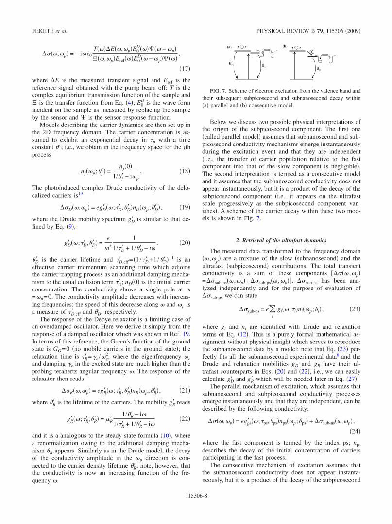
Below we discuss two possible physical interpretations ofthe origin of the subpicosecond component. The first onecalled parallel model assumes that subnanosecond and sub-picosecond conductivity mechanisms emerge instantaneouslyduring the excitation event and that they are independenti.e., the transfer of carrier population relative to the fastcomponent into that of the slow component is negligible.The second interpretation is termed as a consecutive modeland it assumes that the subnanosecond conductivity does notappear instantaneously, but it is a product of the decay of thesubpicosecond component i.e., it appears on the ultrafastscale progressively as the subpicosecond component van-ishes. A scheme of the carrier decay within these two mod-els is shown in Fig. 7.
2. Retrieval of the ultrafast dynamics
The measured data transformed to the frequency domain ,p are a mixture of the slow subnanosecond and theultrafast subpicosecond contributions. The total transientconductivity is a sum of these components ,p=sub-ns ,p+sub-ps ,p. sub-ns has been ana-lyzed independently and for the purpose of evaluation ofsub-ps we can state
sub-ns = ei
gi;inip;i , 23
where gi and ni are identified with Drude and relaxationterms of Eq. 12. This is a purely formal mathematical as-signment without physical insight which serves to reproducethe subnanosecond data by a model; note that Eq. 23 per-fectly fits all the subnanosecond experimental data6 and theDrude and relaxation mobilities gD and gR have their ul-trafast counterparts in Eqs. 20 and 22, i.e., we can easilycalculate gD and gR which will be needed later in Eq. 27.
The parallel mechanism of excitation, which assumes thatsubnanosecond and subpicosecond conductivity processesemerge instantaneously and that they are independent, can bedescribed by the following conductivity:
,p = egps ;ps,psnpsp;ps + sub-ns,p ,
24
where the fast component is termed by the index ps; npsdescribes the decay of the initial concentration of carriersparticipating in the fast process.
The consecutive mechanism of excitation assumes thatthe subnanosecond conductivity does not appear instanta-neously, but it is a product of the decay of the subpicosecond
Dθ′Hθ
(a)
Dθ ′′
Hθ
(b)
FIG. 7. Scheme of electron excitation from the valence band andtheir subsequent subpicosecond and subnanosecond decay withina parallel and b consecutive model.
FEKETE et al. PHYSICAL REVIEW B 79, 115306 2009
115306-8
component. Assuming the photoexcitation event is instanta-neous the conductivity owing to the fast component reads
sub-ps,p = en0gps ;ps,psYpexp− p/ps ,
25
where Y is the Heaviside function. The subnanosecond con-tribution appears on the ultrafast scale progressively as thesubpicosecond component vanishes,
sub-ns,p = eYpn0i
i
i − ps
gi;i,iexp− p/i
− gi;i,psexp− p/ps . 26
Taking into account the fact that gi ;i ,igi ;i forthe subnanosecond components where ii we obtain forthe total transient conductivity in the ,p space
,p = egps ;ps,psnp;ps
+ ei
i
i − psgi;inip;i
− gi;ps,psnp;ps . 27
The ultrafast onset of the slowly decaying component is ac-counted for by the right-most term of this equation.
The parameters relevant for the subpicosecond dynamicsare then allowed to vary in the fitting procedure while theparameters relative to the slow decay are held fixed. Thesubnanosecond and ns conductivity dominates around p0 while the subpicosecond conductivity extends muchmore in the p direction. Here we are interested in the sub-picosecond dynamics, therefore areas p /20.1 THzwere ignored in our fits.
3. Results and interpretation
The subpicosecond response was measured in the collin-ear experimental setup in Fig. 2b to achieve the ultimatetime resolution. Our measurements and analysis followed theprocedure described in Ref. 18. A set of transient wave formsE ,p was measured for several pump-probe delays toobtain a dense 2D grid of data. Typically, we obtained a gridwith the dimensions of 1012 ps 100120 points forthe 800 nm excitation and a grid with the dimensions of 65 ps 6050 points for the 400 nm excitation.
An example of the measured conductivity in the 2D fre-quency domain is shown in Fig. 8a. The spectra consist ofseveral segments, representing experimentally accessibleareas.20 The measured data transformed to the frequency do-main ,p are a mixture of the slow subnanosecond andthe ultrafast subpicosecond contributions and we retrievethe parameters of the ultrafast component following the pro-cedure described in the previous paragraph.
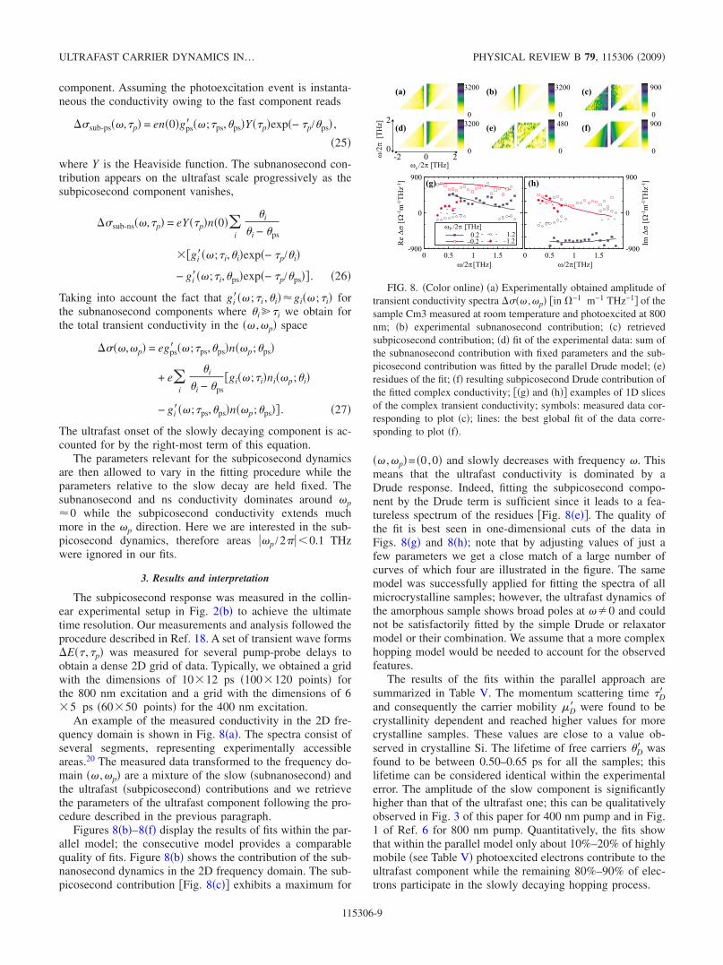
Figures 8b–8f display the results of fits within the par-allel model; the consecutive model provides a comparablequality of fits. Figure 8b shows the contribution of the sub-nanosecond dynamics in the 2D frequency domain. The sub-picosecond contribution Fig. 8c exhibits a maximum for
,p= 0,0 and slowly decreases with frequency . Thismeans that the ultrafast conductivity is dominated by aDrude response. Indeed, fitting the subpicosecond compo-nent by the Drude term is sufficient since it leads to a fea-tureless spectrum of the residues Fig. 8e. The quality ofthe fit is best seen in one-dimensional cuts of the data inFigs. 8g and 8h; note that by adjusting values of just afew parameters we get a close match of a large number ofcurves of which four are illustrated in the figure. The samemodel was successfully applied for fitting the spectra of allmicrocrystalline samples; however, the ultrafast dynamics ofthe amorphous sample shows broad poles at 0 and couldnot be satisfactorily fitted by the simple Drude or relaxatormodel or their combination. We assume that a more complexhopping model would be needed to account for the observedfeatures.
The results of the fits within the parallel approach aresummarized in Table V. The momentum scattering time Dand consequently the carrier mobility D were found to becrystallinity dependent and reached higher values for morecrystalline samples. These values are close to a value ob-served in crystalline Si. The lifetime of free carriers D wasfound to be between 0.50–0.65 ps for all the samples; thislifetime can be considered identical within the experimentalerror. The amplitude of the slow component is significantlyhigher than that of the ultrafast one; this can be qualitativelyobserved in Fig. 3 of this paper for 400 nm pump and in Fig.1 of Ref. 6 for 800 nm pump. Quantitatively, the fits showthat within the parallel model only about 10%–20% of highlymobile see Table V photoexcited electrons contribute to theultrafast component while the remaining 80%–90% of elec-trons participate in the slowly decaying hopping process.
FIG. 8. Color online a Experimentally obtained amplitude oftransient conductivity spectra ,p in −1 m−1 THz−1 of thesample Cm3 measured at room temperature and photoexcited at 800nm; b experimental subnanosecond contribution; c retrievedsubpicosecond contribution; d fit of the experimental data: sum ofthe subnanosecond contribution with fixed parameters and the sub-picosecond contribution was fitted by the parallel Drude model; eresidues of the fit; f resulting subpicosecond Drude contribution ofthe fitted complex conductivity; g and h examples of 1D slicesof the complex transient conductivity; symbols: measured data cor-responding to plot c; lines: the best global fit of the data corre-sponding to plot f.
ULTRAFAST CARRIER DYNAMICS IN… PHYSICAL REVIEW B 79, 115306 2009
115306-9
In the frame of the consecutive approach all the photoex-cited electrons participate in the ultrafast process immedi-ately after the excitation p=0 and similarly as in the caseof the parallel model they are found to exhibit the Drudebehavior for all crystalline samples. The experimental datawere successfully fitted within this model and their mobilitywas observed to be significantly lower as compared to that ofthe parallel approach; we found D 10 fs and D70 cm2 /Vs for all microcrystalline samples. Within theconsecutive model the decay times D display the same val-ues as for the parallel model D , D 0.55–0.65 ps.
IV. DISCUSSION
The structure of c-Si:H consists of large grains sur-rounded by an amorphous tissue. The large grains with sizeof hundreds of nm are built of small grains with typical sizeof about 20 nm.25 These two distinct length scales appearas different time scales in our time-resolved experiments.A characteristic time of the subpicosecond dynamics isD 0.5 ps Table V. If we assume that the diffusionof the photogenerated electrons is the same as in c-SiD=36 cm2 s−1, we find a characteristic length of DD40 nm. The subpicosecond dynamics is then determinedby intrinsic properties of small grains and/or by their bound-aries, while the large grain boundaries may control only thesubnanosecond dynamics.
Due to the inhomogeneity of c-Si:H, one should care-fully consider which parts of the sample can significantlycontribute to the transient conductivity. Upon excitation at800 nm the amorphous tissue absorbs considerably less thanthe c-Si and c-Si:H Ref. 16; however, the reverse canhold for excitation at 400 nm, where the beam is absorbedwithin a very thin layer which is almost crystalline in somesamples for excitation at the front surface. This means thatfor both excitation wavelengths it is reasonable to assumethat the majority of the pump photons is absorbed in crystal-line parts of the films. Since the transient conductivity ofthe amorphous sample is smaller than that of the c onesFig. 3, we neglect any possible contribution due to directexcitation of amorphous tissue when discussing the proper-ties of c samples.
The mobility of holes in c-Si is approximately four timeslower than the mobility of electrons.26 The contribution of
electrons to the transient conductivity spectra is then ex-pected to be dominant; however, there may be a small con-tribution of holes in the measured spectra as well. The sub-sequent discussion considers electrons only, but similararguments can be reused to include also the hole dynamics.
A. Subpicosecond dynamics in c samples
Within the parallel model, the ultrafast component of theconductivity spectra is accounted for by a single Drude termwith a mobility comparable to that found in c-Si. From theamplitude of the subpicosecond conductivity and from theknown excitation fluence we can estimate that within thishypothesis only a very low fraction of the absorbed photonswould generate the mobile electrons e.g., 20% at 800 nmand 8% at 400 nm for the Cm3 sample. Since we haveruled out that photons are absorbed in the amorphous tissue,the hypothesis of the parallel model would require to admitthat a large majority of photogenerated electrons is capturedinto hopping states on a time scale shorter than the temporalresolution of the setup 50 fs while only a minority iscaptured with a quite longer time-constant of 0.5 ps orthat localized hopping states are populated directly duringthe photoexcitation event.
In the consecutive model, we start from the assumptionthat all absorbed photons generate mobile electrons in theX valley of Si. The ultrafast drop in the conductivity thenrepresents capturing the electrons in hopping states. Theincrease in occupation of the hopping states appears as asubpicosecond rise of the subnanosecond component. Theconductivity of the nascent free electrons is well describedby a Drude model with a low initial mobility D70 cm2 V−1 s−1.
Both hypotheses lead to fits with a comparable quality.We believe that the consecutive model more properly reflectsthe photoinduced dynamics. A capture time shorter than 100fs seems to interfere with the fact that c-Si:H is a materialwith a high fraction of well crystalline component—mostultrafast materials are highly defective and rarely show suchshort lifetimes.27 Moreover, the photogenerated carriers havevery high excess energy which makes their efficient capturedifficult.
Such discrepancies are not encountered in the consecutivemodel, and we show below that the speed of decay and themagnitude of the mobility are well explained by the fact thatthe carriers are initially hot. The initial electron temperaturein c-Si upon photoexcitation at 800 nm is Te,02000 K, andthe cooling occurs with a rate of a few hundreds of fs.28,29
The mobility D then corresponds to electron temperatureTe=1000 K, which represents a reasonable estimate of anaverage electron temperature during the subpicosecond de-cay. Note that we did not observe any significant differenceeither in amplitude or in time constants in the ultrafast partof pump-probe scans within the broad investigated tempera-ture range. The independence of these results on the latticetemperature corroborates the conclusion that hot carriers areresponsible for the subpicosecond component. If the carrierswere equilibrated with lattice then their mobility, decay time,and the ultrafast conductivity amplitude would be stronglytemperature dependent.
TABLE V. Parameters of the ultrafast subpicosecond conductiv-ity at 300 K for both 800 and 400 nm excitation; parallel model,fitting using a Drude term Eq. 19.
Sample
800 nm 400 nm
Dfs
Dcm2 /Vs
Dps
Dfs
Dcm2 /Vs
Dps
Cm3 90 610 0.55 55 370 0.55
Cm2 60 410 0.65 80 540 0.60
Cm1 55 370 0.55 70 470 0.55
Cm3BS 45 300 0.50
FEKETE et al. PHYSICAL REVIEW B 79, 115306 2009
115306-10
Although we are far from equilibrium, we tentatively ap-ply Einstein relation to estimate the diffusion coefficient:D=D kBTe /e05 cm2 s−1. With these values, the diffusion
length DD is less than 17 nm, and it delimits the dis-tance through which the electrons can travel prior to theirrelaxation to states with much lower mobility. The similarityof the small grain size and the diffusion length argues for anexplanation that these states are located at the small-grainboundaries. Jepsen et al.30 previously performed optical-pump–terahertz probe experiments without spectral reso-lution in c-Si:H and observed a similar decay time of 0.7ps, which they assigned to capture in trapping states. In ourstudy, we have an additional spectral resolution which allowsus to demonstrate that there is a slower transport processbetween these states which is responsible for the subnano-second conductivity discussed in the next section. Ultrafastdynamics in microcrystalline silicon was studied also by op-tical transient absorption technique;31 in this work the au-thors observed a fast 240-fs component which was indepen-dent of the crystallinity degree of the investigated samples.This component has been attributed to the intraband relax-ation of hot carriers within crystallites. This component, evenif twice faster, should have the same origin as that observedin our experiments.
B. Subnanosecond dynamics in c :H samples
It has been demonstrated in the previous section that thecharacter of the carrier transport changes at about 0.6 ps afterphotoexcitation event. The observed slow component decayson a subnanosecond time scale in agreement with previouslypublished data obtained by optical transient gratingtechnique.32 The aim of this paragraph is to attribute theobserved signal to the underlying transport processes.
1. Absence of Drude contribution
In our previous paper6 we showed that the room-temperature spectra can be well fitted by a sum of threeterms: a Drude term, a relaxation in the 3–7 terahertz rangefast relaxation and a relaxation in the subterahertz rangeslow relaxation. We found that all the temperature depen-dent data can be fitted by this model; the amplitudes of theseterms as it can be expected from the experimental datashown in Fig. 6 decrease with decreasing temperature. Theaim of this paragraph is to refute this hypothesis with physi-cal arguments.
It was shown that no fast relaxation contribution is ob-served in the amorphous sample and that its characteristicdecay time in microcrystalline samples is similar to that ofthe Drude term.6 This suggested us a hypothesis that theprocess could be connected to the localization of free carrierswithin nanoscopic crystalline grains. Similar picture hasbeen recently proposed to explain photoexcited carrier dy-namics in Si nanocrystals embedded in SiO2 matrix.33 Withinsuch a model the conduction-band carriers would exhibit twofingerprints in the spectra: a localized contribution occurringat 3–7 terahertz and a delocalized Drude-like one. We madean attempt to model the transport of electrons inter and in-tragrains using a Monte Carlo method. In brief, we simulated
a thermal motion of free electrons in spherical potential wellsrepresenting crystalline grains. Inside the spheres the elec-tron momentum randomly changes with a mean time s be-tween the scattering events. This scattering time, which char-acterizes in fact the microscopic intragrain mobility, istemperature dependent similarly as that in crystallinesilicon;26,34 in our simulations we used the room-temperaturevalue of the crystalline silicon mobility and its temperaturedependence which was reported for moderately dopedsilicon.26 Upon hitting the grain boundary an electron canenter into the neighboring grain with some probability p de-scribing the permeability of the boundaries for conductionelectrons. The spectral response of electrons was then cal-culated using Kubo formula;35 more details are provided inRef. 36.
We found that our room-temperature data are quantita-tively well described by this model provided the involvedgrains have a 20–30 nm size and provided the permeabilityof the grain boundaries is p1% i.e., one particle out of100 will pass through the boundary without feeling the lo-calization. The results are shown in Fig. 9. When largergrains and/or higher permeability of the grain boundaries areintroduced into the simulation the resulting dc mobilityreaches significantly higher values and cannot reproduce theexperimental data. The found extent of the carrier localiza-tion 20–30 nm then implies the leading role of the so-called“small grains”37 in this process. On the other hand, thesesmall grains cause only a small perturbation in the drift mo-bility of free electrons.25 This is in a contrast with the re-quirement of our simulation of the very low permeability ofthe grain boundaries for conduction electrons.
Even more severe discrepancy is found if we compare theresults of the low-temperature experiments with the resultsof the simulation. Besides the temperature dependent intra-
10-1 100 101
Frequency (THz)
200
150
100
50
0
-50
-100
-150
-200
Img
(cm
2 V-1
s-1)
Re
g(c
m2 V
-1s-1
)
300 K100 K
20 K
FIG. 9. Color online Mobility spectra of the subnanosecondcontribution pump-probe delay p=50 ps of Cm2 sample for sev-eral temperatures; pump wavelength: 800 nm. Symbols: experimen-tal data, thick lines: results of the Monte Carlo simulation describedin the text grain size 20 nm, grain-boundary permeability 1%, thinlines: extrapolation of the fit of the data by hopping model 13.
ULTRAFAST CARRIER DYNAMICS IN… PHYSICAL REVIEW B 79, 115306 2009
115306-11
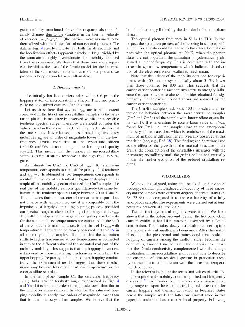
grain mobility mentioned above the response also signifi-cantly changes due to the variation in the thermal velocityof carriers v=3kBTe /m the carriers were assumed to bethermalized with the lattice for subnanosecond process. Thedata in Fig. 9 clearly indicate that both the dc mobility andthe localization effects apparent namely in Im g yielded bythe simulation highly overestimate the mobility deducedfrom the experiment. We deem that these severe discrepan-cies invalidate the use of the Drude model for the interpre-tation of the subnanosecond dynamics in our sample, and wepropose a hopping model as an alternative.
2. Hopping dynamics
The initially hot free carriers relax within 0.6 ps to thehopping states of microcrystalline silicon. There are practi-cally no delocalized carriers after this time.
Let us stress here that H and min are to some extentcorrelated in the fits of microcrystalline samples as the satu-ration plateau is not directly observed within the accessibleterahertz spectral range. Therefore we should consider thevalues found in the fits as an order of magnitude estimates ofthe true values. Nevertheless, the saturated high-frequencymobilities H are an order of magnitude lower than the low-frequency Drude mobilities in the crystalline silicon1400 cm2 /Vs at room temperature for a good qualitycrystal. This means that the carriers in microcrystallinesamples exhibit a strong response in the high-frequency re-gime.
An estimate for Cm2 and Cm3 of min16 fs at roomtemperature corresponds to a cutoff frequency of 10 terahertzand min7 fs obtained at low temperatures corresponds toa cutoff frequency of 22 terahertz. Figure 9 displays an ex-ample of the mobility spectra obtained for Cm2 sample. Thereal part of the mobility exhibits quantitatively the same be-havior in the terahertz spectral range between 20 and 300 K.This indicates that the character of the carrier transport doesnot change with temperature, and it is compatible with thehypothesis of largely dominating hopping process providedour spectral range is close to the high-frequency cut 1 /min.The different slopes of the negative imaginary conductivityfor the room and low temperatures are connected to the shiftof the conductivity minimum, i.e., to the shift of 1 /min withtemperature this trend can be clearly observed in Table IV inall microcrystalline samples. The fact that the saturationshifts to higher frequencies at low temperatures is connectedin turn to the different values of the saturated real part of themobility mobility. This suggests that the hopping of carriersis hindered by some scattering mechanisms which limit theupper hopping frequency and the maximum hopping conduc-tivity; the experimental results suggest that these mecha-nisms may become less efficient at low temperatures in mi-crocrystalline samples.
In the amorphous sample Ca the saturation frequency1 /min falls into the terahertz range as observed in Figs. 4and 5 and it is about an order of magnitude lower than that inthe microcrystalline samples. In addition the saturated hop-ping mobility is nearly two orders of magnitude lower thanthat for the microcrystalline samples. We believe that the
hopping is strongly limited by the disorder in the amorphousphase.
The optical phonon frequency in Si is 16 THz. In thisrespect the saturation process of the hopping in samples witha high crystallinity could be related to the interaction of car-riers with the optical phonon. At 20 K, when the phononstates are not populated, the saturation is systematically ob-served at higher frequency. This is correlated with the in-crease in H at low temperatures which indicates deactiva-tion of the electron-phonon scattering mechanism.
Note that the values of the mobility obtained for experi-ments with 400 nm are systematically about 3–5 lowerthan those obtained for 800 nm. This suggests that thecarrier-carrier scattering mechanisms starts to strongly influ-ence the transport: the terahertz mobilities obtained for sig-nificantly higher carrier concentrations are reduced by thecarrier-carrier scattering.
The Cm3BS sample back side, 400 nm exhibits an in-termediate behavior between the most crystalline samplesCm2 and Cm3 and the sample with intermediate crystallin-ity Cm1. It is interesting to note a large value of 1 /minfound for Cm1, i.e., the sample close to the amorphous/microcrystalline transition, which is reminiscent of the maxi-mum of ambipolar diffusion length typically observed at thistransition see, e.g., Ref. 38. This finding can be rationalizedas the effect of the growth on the internal structure of thegrains: the contribution of the crystallites increases with theincreasing crystallinity until the grains collide and mutuallyhinder the further evolution of the ordered crystalline re-gions.
V. CONCLUSION
We have investigated, using time-resolved terahertz spec-troscopy, ultrafast photoinduced conductivity of three micro-crystalline samples with different degrees of crystallinity 23,58, 73 % and compared it to the conductivity of a fullyamorphous sample. The experiments were carried out at tem-peratures between 300 and 20 K.
Two distinct dynamical regimes were found. We haveshown that in the subpicosecond regime, the hot conductioncarriers exhibit a bandlike transport described by a Drudecontribution. The ultrafast decay is a result of carrier capturein shallow states at small-grain boundaries. After this initialphase—on the picosecond and nanosecond time scales—hopping of carriers among the shallow states becomes thedominating transport mechanism. Our analysis has shownthat the Drude conductivity complemented with the chargelocalization in microcrystalline grains is not able to describethe ensemble of time-resolved spectra: in particular, thesehypotheses are in contradiction with the measured tempera-ture dependence.
In the relevant literature the terms and values of drift andmicroscopic band mobility are distinguished and frequentlydiscussed.39 The former one characterizes a macroscopiclong-range transport between electrodes, and it accounts forcarrier trapping and thermal activation in localized statesacross the sample while the latter one investigated in thispaper is understood as a carrier local property. Following
FEKETE et al. PHYSICAL REVIEW B 79, 115306 2009
115306-12
our experiments the low-frequency mobility of the observedhopping process is of the order of 20 cm2 /Vs. This value isin agreement with the estimations of the microscopic mobil-ity obtained by means of transient photocurrent or time-of-flight spectroscopies in c-Si:H samples. The results of thiswork then indicate that the microscopic mobility is of hop-ping nature in microcrystalline silicon.
ACKNOWLEDGMENTS
We thank J. Kočka and M. Ledinský for valuable discus-sions. This research was supported by the Ministry of Edu-cation Project No. LC06040 and by the Academy of Sci-ences of the Czech Republic Project Nos. A100100902,AVOZ10100520, and AVOZ10100521.
*[email protected] A. Shah, P. Torres, R. Tscharner, N. Wyrsch, and H. Keppner,
Science 285, 692 1999.2 S. Reynolds, Mater. Res. Soc. Symp. Proc. 910, 3 2007.3 M. Brinza, J. Willekens, M. L. Benkhedir, E. V. Emelianova, and
G. J. Adriaenssens, J. Mater. Sci.: Mater. Electron. 16, 7032005.
4 C. A. Schmuttenmaer, Chem. Rev. 104, 1759 2004.5 F. A. Hegmann, O. Ostroverkhova, and D. G. Cooke, Photophys-
ics of Molecular Materials Wiley-VCH, New York, 2006,Chap. 7, pp. 367–428.
6 L. Fekete, H. Němec, F. Kadlec, P. Kužel, J. Stuchlík, A. Fejfar,and J. Kočka, J. Non-Cryst. Solids 352, 2846 2006.
7 H. Fujiwara, M. Kondo, and A. Matsuda, Phys. Rev. B 63,115306 2001.
8 S. Koynov, S. Grebner, P. Radojkovic, E. Hartmann, R. Schwarz,L. Vasilev, R. Krankenhagen, I. Sieber, W. Henrion, and M.Schmidt, J. Non-Cryst. Solids 198-200, 1012 1996.
9 A. Fejfar, T. Mates, O. Čertík, B. Rezek, J. Stuchlík, I. Pelant,and J. Kočka, J. Non-Cryst. Solids 338-340, 303 2004.
10 M. Ledinský, L. Fekete, J. Stuchlík, T. Mates, A. Fejfar, and J.Kočka, J. Non-Cryst. Solids 352, 1209 2006.
11 M. Ledinský, A. Vetushka, J. Stuchlík, T. Mates, A. Fejfar, J.Kočka, and J. Štěpánek, J. Non-Cryst. Solids 354, 2253 2008.
12 M. Kondo, Y. Toyoshima, A. Matsuda, and K. Ikuta, J. Appl.Phys. 80, 6061 1996.
13 D. Han, K. Wang, J. M. Owens, L. Gedvilas, B. Nelson, H.Habuchi, and M. Tanaka, J. Appl. Phys. 93, 3776 2003.
14 C. Smit, R. A. C. M. M. van Swaaij, H. Donker, A. M. H. N.Petit, W. M. M. Kessels, and M. C. M. van de Sanden, J. Appl.Phys. 94, 3582 2003.
15 R. Tsu, J. Gonzalez-Hernandez, S. S. Chao, S. C. Lee, and K.Tanaka, Appl. Phys. Lett. 40, 534 1982.
16 A. Poruba, J. Springer, L. Mullerova, A. Beitlerova, M. Vaněček,N. Wyrsch, and A. Shah, J. Non-Cryst. Solids 338-340, 2222004.
17 A. Nahata, A. S. Weling, and T. F. Heinz, Appl. Phys. Lett. 69,2321 1996.
18 H. Němec, F. Kadlec, C. Kadlec, P. Kužel, and P. Jungwirth, J.Chem. Phys. 122, 104504 2005.
19 H. Němec, F. Kadlec, S. Surendran, P. Kužel, and P. Jungwirth, J.
Chem. Phys. 122, 104503 2005.20 H. Němec, F. Kadlec, and P. Kužel, J. Chem. Phys. 117, 8454
2002.21 P. Kužel, F. Kadlec, and H. Němec, J. Chem. Phys. 127, 024506
2007.22 S. R. Elliott, Adv. Phys. 36, 135 1987.23 J. C. Dyre, J. Appl. Phys. 64, 2456 1988.24 J. Kudrna, P. Malý, F. Trojánek, J. Štěpánek, T. Lechner, I. Pel-
ant, J. Meier, and U. Kroll, Mater. Sci. Eng., B 69-70, 2382000.
25 J. Kočka, H. Stuchlíková, J. Stuchlík, B. Rezek, T. Mates, V.Švrček, P. Fojtik, I. Pelant, and A. Fejfar, J. Non-Cryst. Solids299-302, 355 2002.
26 F. J. Morin and J. P. Maita, Phys. Rev. 96, 28 1954.27 J.-L. Coutaz, Acta Phys. Pol. A 102, 495 2002.28 A. J. Sabbah and D. M. Riffe, Phys. Rev. B 66, 165217 2002.29 J. R. Goldman and J. A. Prybyla, Phys. Rev. Lett. 72, 1364
1994.30 P. Uhd Jepsen, W. Schairer, I. H. Libon, U. Lemmer, N. E.
Hecker, M. Birkholz, K. Lips, and M. Schall, Appl. Phys. Lett.79, 1291 2001.
31 K. E. Myers, Q. Wang, and S. L. Dexheimer, Phys. Rev. B 64,161309R 2001.
32 J. Kudrna, F. Trojánek, P. Malý, and I. Pelant, Appl. Phys. Lett.79, 626 2001.
33 D. G. Cooke, A. N. MacDonald, A. Hryciw, J. Wang, Q. Li, A.Meldrum, and F. A. Hegmann, Phys. Rev. B 73, 193311 2006.
34 P. Norton, T. Braggins, and H. Levinstein, Phys. Rev. B 8, 56321973.
35 R. Kubo, Rep. Prog. Phys. 29, 255 1966.36 H. Němec, P. Kužel, and V. Sundström, Phys. Rev. B to be
published.37 J. Kočka, H. Stuchlíková, J. Stuchlík, B. Rezek, V. Švrček, P.
Fojtík, I. Pelant, and A. Fejfar, in Polycrystalline Semiconduc-tors: VI. Bulk Materials, Thin Films, and Devices, edited by O.Bonnaud, T. Mohammed-Brahim, H. P. Strunk, and J. H.Werner, Solid State Phenomena Vols. 80–81 Scitech, Uettikonam See, Switzerland, 2001, pp. 213–224.
38 J. Kočka, T. Mates, H. Stuchlíková, J. Stuchlík, and A. Fejfar,Thin Solid Films 501, 107 2006.
39 E. A. Schiff, J. Phys.: Condens. Matter 16, S5265 2004.
ULTRAFAST CARRIER DYNAMICS IN… PHYSICAL REVIEW B 79, 115306 2009
115306-13