ultrafast terahertz nanoelectronics lab jae-seok kim 1 terabus : terabit/second-class card-level...
Post on 21-Dec-2015
215 views
TRANSCRIPT
Ultrafast Terahertz Nanoelectronics Lab
Jae-seok Kim
1
Terabus : Terabit/Second-Class Card-Level Op-tical Interconnect Technologies
Lautent Schares, Jeffrey A.Kash, …
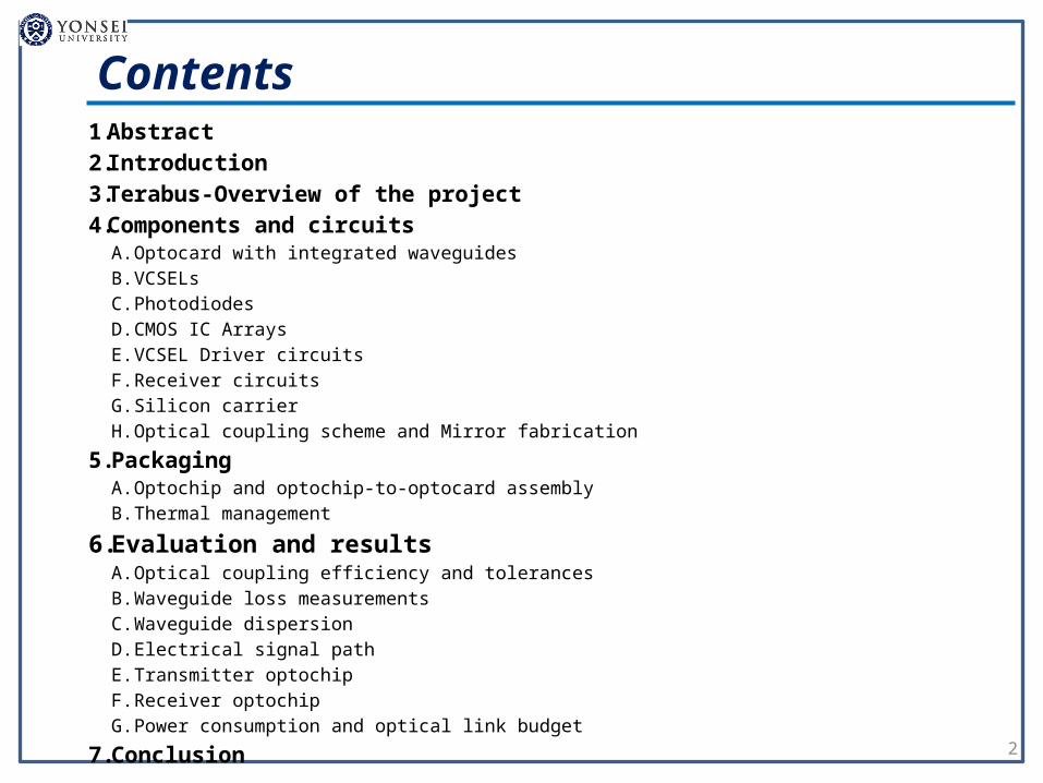
Contents1.Abstract
2.Introduction
3.Terabus-Overview of the project
4.Components and circuitsA. Optocard with integrated waveguidesB. VCSELsC. PhotodiodesD. CMOS IC ArraysE. VCSEL Driver circuitsF. Receiver circuitsG. Silicon carrierH. Optical coupling scheme and Mirror fabrication
5. PackagingA. Optochip and optochip-to-optocard assemblyB. Thermal management
6. Evaluation and resultsA. Optical coupling efficiency and tolerancesB. Waveguide loss measurementsC. Waveguide dispersionD. Electrical signal pathE. Transmitter optochipF. Receiver optochipG. Power consumption and optical link budget
7. Conclusion2
Abstract
3
In the “Terabus” optical interconnect program, optical data bus technologies are developed
→ For terabit/second chip-to-chip data transfers over organic cards within high-perfor-mance servers, switch routers, and other intensive computing systems
Chip-like optoelectronic packaging structure(Optochip), assembled directly onto an organic card(Optocard)
Vertical-cavity surface emitting laser(VCSEL) and photodiode arrays(4×12) are flip-chip bonded to the driver and receiver IC arrays implemented in 0.13-μm CMOS
The IC arrays are in turn flip-chip assembled onto a 1.2-cm2 silicon carrier in-terposer to complete the transmitter and receiver Optochips
The organic Optocard incorporates 48 parallel multimode optical waveguides on a 62.5-μm pitch
based on a single-lens array etched onto the backside of the optoelectronic arrays and on 45 ◦ mirrors in the waveguides
Transmitter and receiver operation is demonstrated up to 20 and 14Gb/s per channel
The power dissipation of 10-Gb/s single-channel links over multimode fiber is as low as 50 mW
Introduction
4
The bandwidth and density requirements for interconnects within high-performance computing systems are growing fast, owing to increasing chip speeds, wider buses, and larger numbers of processors per system
Parallel optical interconnects (POIs) promise to enable links with terabit/second-class data transfer capability in a small form factor, at higher density and with less con-straint on link length than electrical interconnects
→ Several POIs based on multimode fiber (MMF) ribbons >100-Gb/s-range→ for links between racks of servers or between boards, over lengths ranging from about one meter
up to hundreds of meters If optics are to compete with copper-based electrical backplanes for on-board inter-
connects→ significant advances in terms of speed, power consumption, density, and cost A number of research programs have started to develop components and work on the
integration for high-density on-board optical interconnects it is challenging to fulfill all these requirements together, and to develop simple pack-
aging processes that permit the dense integration of high-speed components The Terabus project addresses these packaging, density, and speed issues, and a
complete technology set is developed in order to realize a terabit/second-class optical bus for chip-to-chip interconnects on printed circuit boards
The strategy for reducing the size and increasing the speed is to develop optoelec-tronic modules that simultaneously push the data rate per line up to 20 Gb/s and the number of channels in the bus up to 48 in order to achieve data transfers approaching 0.5–1 Tb/s
Terabus-Overview of the project
5
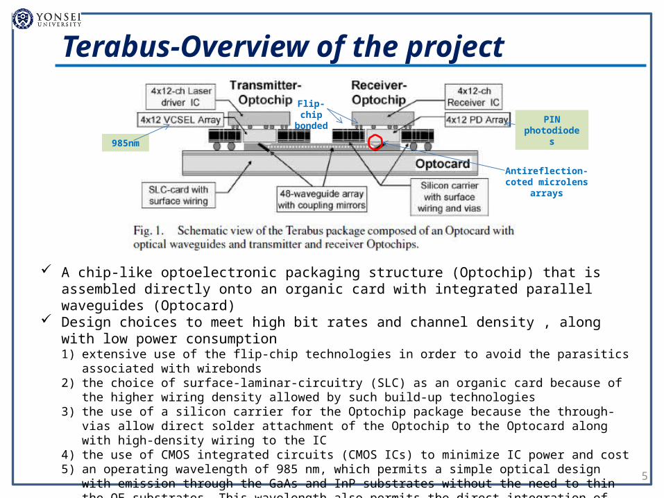
A chip-like optoelectronic packaging structure (Optochip) that is assembled directly onto an organic card with integrated parallel waveguides (Optocard)
Design choices to meet high bit rates and channel density , along with low power consump-tion1) extensive use of the flip-chip technologies in order to avoid the parasitics associated with wirebonds2) the choice of surface-laminar-circuitry (SLC) as an organic card because of the higher wiring density al-
lowed by such build-up technologies3) the use of a silicon carrier for the Optochip package because the through-vias allow direct solder at-
tachment of the Optochip to the Optocard along with high-density wiring to the IC4) the use of CMOS integrated circuits (CMOS ICs) to minimize IC power and cost5) an operating wavelength of 985 nm, which permits a simple optical design with emission through the
GaAs and InP substrates without the need to thin the OE substrates. This wavelength also permits the direct integration of lenses into the substrates
985nm
PIN photodi-odes
Flip-chip bonded
Antireflection-coted microlens arrays
Components and circuits
6
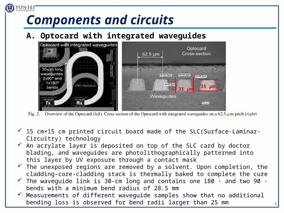
15 cm×15 cm printed circuit board made of the SLC(Surface-Laminar-Circuitry) technology An acrylate layer is deposited on top of the SLC card by doctor blading, and waveguides are
photolithographically patterned into this layer by UV exposure through a contact mask The unexposed regions are removed by a solvent. Upon completion, the cladding-core-
cladding stack is thermally baked to complete the cure The waveguide link is 30-cm long and contains one 180 ◦ and two 90 ◦ bends with a mini-
mum bend radius of 28.5 mm Measurements of different waveguide samples show that no additional bending loss is ob-
served for bend radii larger than 25 mm
A. Optocard with integrated waveguides
35 μm 35 μm
B. VCSELs(Vertical Cavity Surface Emitting Laser)
7
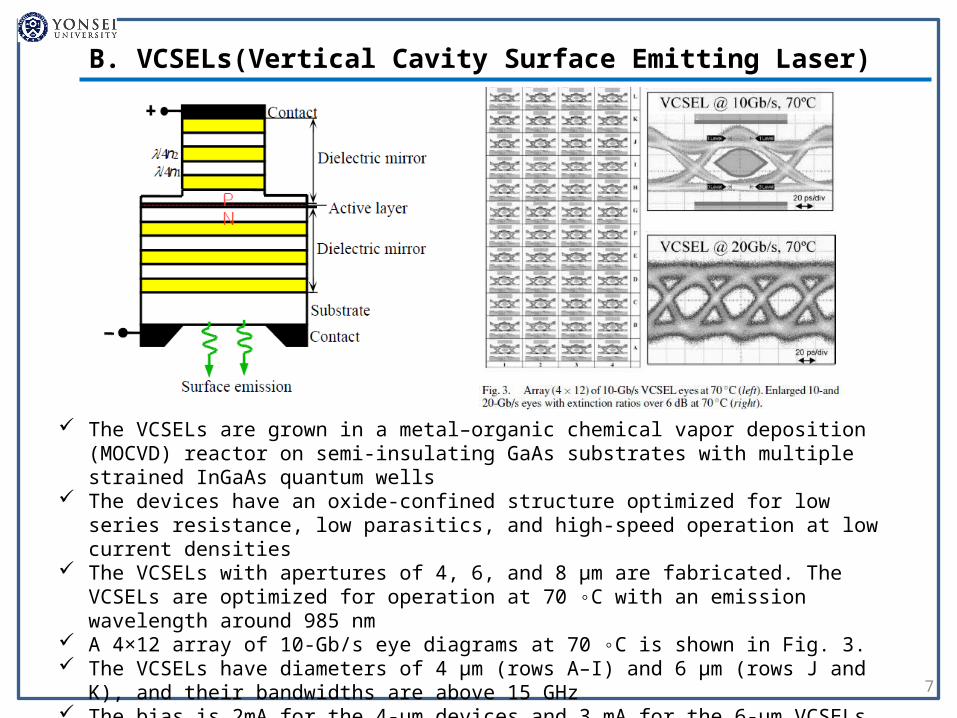
The VCSELs are grown in a metal–organic chemical vapor deposition (MOCVD) reactor on semi-insulating GaAs substrates with multiple strained InGaAs quantum wells
The devices have an oxide-confined structure optimized for low series resistance, low para-sitics, and high-speed operation at low current densities
The VCSELs with apertures of 4, 6, and 8 μm are fabricated. The VCSELs are optimized for operation at 70 ◦C with an emission wavelength around 985 nm
A 4×12 array of 10-Gb/s eye diagrams at 70 ◦C is shown in Fig. 3. The VCSELs have diameters of 4 μm (rows A–I) and 6 μm (rows J and K), and their band-
widths are above 15 GHz The bias is 2mA for the 4-μm devices and 3 mA for the 6-μm VCSELs Fig. 3 also shows a zoom on a 10- and a 20-Gb/s eye of a 6-μm VCSEL at 70 ◦C
C. Photodiodes
8
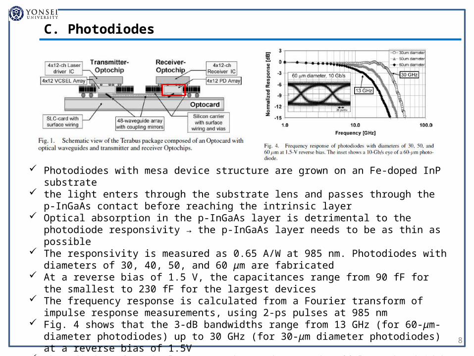
Photodiodes with mesa device structure are grown on an Fe-doped InP substrate the light enters through the substrate lens and passes through the p-InGaAs contact before
reaching the intrinsic layer Optical absorption in the p-InGaAs layer is detrimental to the photodiode responsivity → the
p-InGaAs layer needs to be as thin as possible The responsivity is measured as 0.65 A/W at 985 nm. Photodiodes with diameters of 30, 40,
50, and 60 μm are fabricated At a reverse bias of 1.5 V, the capacitances range from 90 fF for the smallest to 230 fF for
the largest devices The frequency response is calculated from a Fourier transform of impulse response mea-
surements, using 2-ps pulses at 985 nm Fig. 4 shows that the 3-dB bandwidths range from 13 GHz (for 60-μm-diameter photodi-
odes) up to 30 GHz (for 30-μm diameter photodiodes) at a reverse bias of 1.5V Photodiodes of optimal size can be used to trade off lower bandwidth for increased align-
ment tolerance
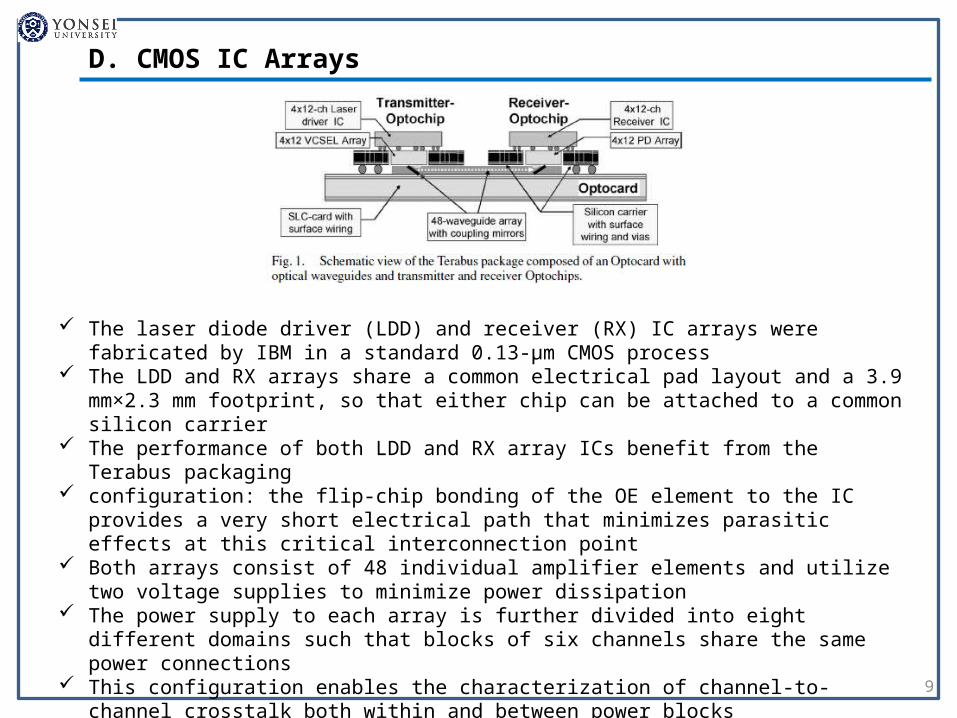
D. CMOS IC Arrays
9
The laser diode driver (LDD) and receiver (RX) IC arrays were fabricated by IBM in a stan-dard 0.13-μm CMOS process
The LDD and RX arrays share a common electrical pad layout and a 3.9 mm×2.3 mm foot-print, so that either chip can be attached to a common silicon carrier
The performance of both LDD and RX array ICs benefit from the Terabus packaging configuration: the flip-chip bonding of the OE element to the IC provides a very short electri -
cal path that minimizes parasitic effects at this critical interconnection point Both arrays consist of 48 individual amplifier elements and utilize two voltage supplies to
minimize power dissipation The power supply to each array is further divided into eight different domains such that
blocks of six channels share the same power connections This configuration enables the characterization of channel-to-channel crosstalk both within
and between power blocks The on-chip power supply decoupling is extensively employed and the layout of the ampli -
fier array elements is carefully considered to minimize intra and interchannel crosstalk
E. VCSEL driver circuits
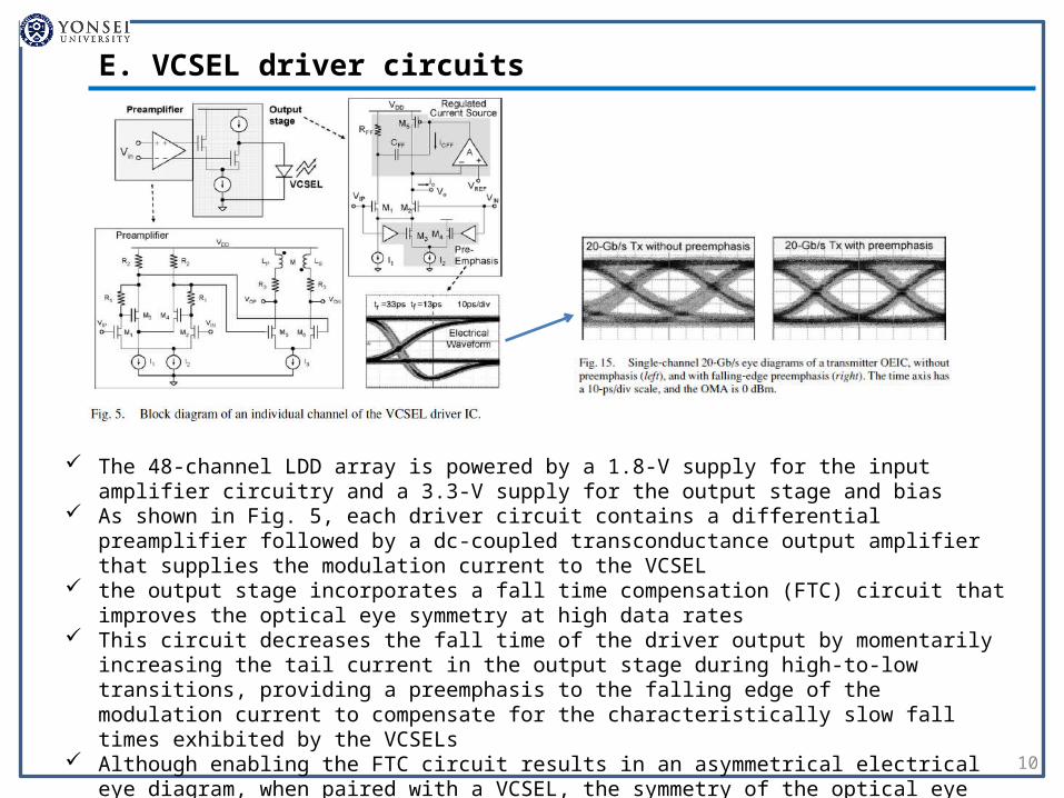
10
The 48-channel LDD array is powered by a 1.8-V supply for the input amplifier circuitry and a 3.3-V supply for the output stage and bias
As shown in Fig. 5, each driver circuit contains a differential preamplifier followed by a dc-coupled transconductance output amplifier that supplies the modulation current to the VCSEL
the output stage incorporates a fall time compensation (FTC) circuit that improves the optical eye symmetry at high data rates
This circuit decreases the fall time of the driver output by momentarily increasing the tail current in the output stage during high-to-low transitions, providing a preemphasis to the falling edge of the modulation current to compensate for the characteristically slow fall times exhibited by the VC-SELs
Although enabling the FTC circuit results in an asymmetrical electrical eye diagram, when paired with a VCSEL, the symmetry of the optical eye diagram is improved, as Fig. 15 in Section V-E illus-trates
F. Receiver circuits
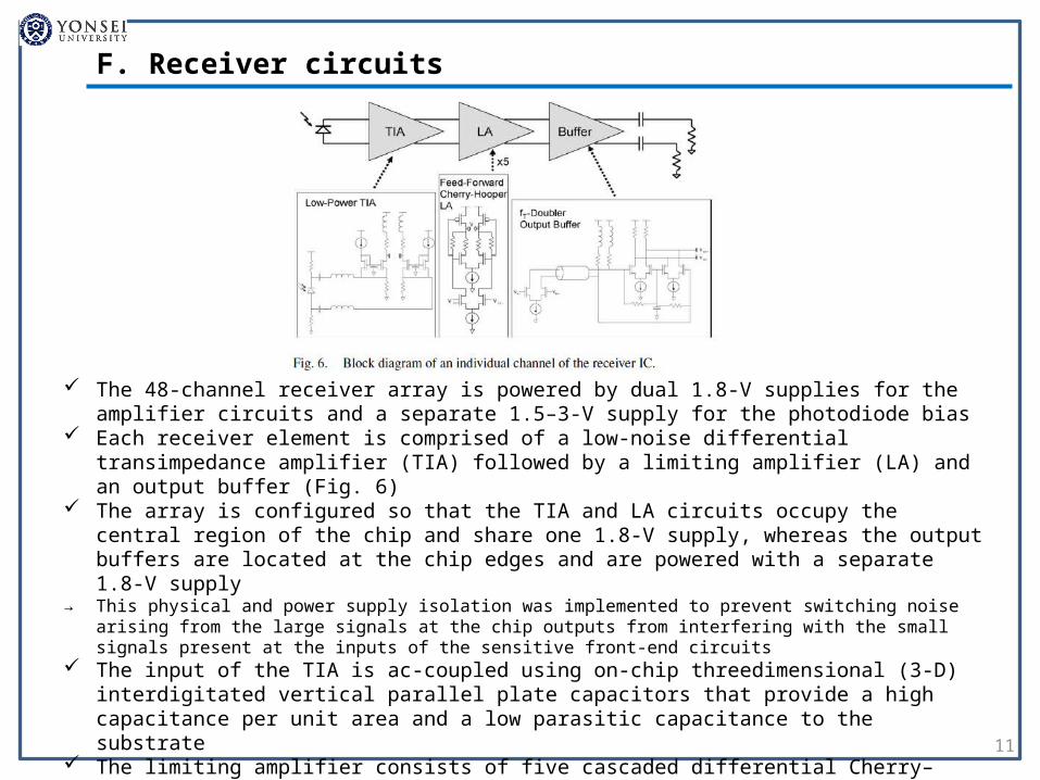
11
The 48-channel receiver array is powered by dual 1.8-V supplies for the amplifier circuits and a separate 1.5–3-V supply for the photodiode bias
Each receiver element is comprised of a low-noise differential transimpedance amplifier (TIA) fol-lowed by a limiting amplifier (LA) and an output buffer (Fig. 6)
The array is configured so that the TIA and LA circuits occupy the central region of the chip and share one 1.8-V supply, whereas the output buffers are located at the chip edges and are powered with a separate 1.8-V supply
→ This physical and power supply isolation was implemented to prevent switching noise arising from the large signals at the chip outputs from interfering with the small signals present at the inputs of the sensitive front-end circuits
The input of the TIA is ac-coupled using on-chip threedimensional (3-D) interdigitated vertical paral-lel plate capacitors that provide a high capacitance per unit area and a low parasitic capacitance to the substrate
The limiting amplifier consists of five cascaded differential Cherry–Hooper gain stages with an off-set cancellation feedback loop around the final four stages
The output buffer circuit also employs inductive peaking at its input, and is designed to drive an ac-coupled, off-chip 50-Ω load
G. Silicon carrier
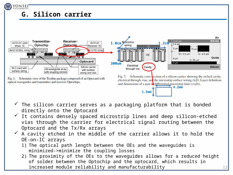
12
The silicon carrier serves as a packaging platform that is bonded directly onto the Optocard It contains densely spaced microstrip lines and deep silicon-etched vias through the carrier
for electrical signal routing between the Optocard and the Tx/Rx arrays A cavity etched in the middle of the carrier allows it to hold the OE-on-IC arrays
1) The optical path length between the OEs and the waveguides is minimized->minimize the coupling losses
2) The proximity of the OEs to the waveguides allows for a reduced height of solder between the Optochip and the optocard, which results in increased module reliability and manufacturability
1.0cm 1.2cm
300um
1.5mm
4.2mm
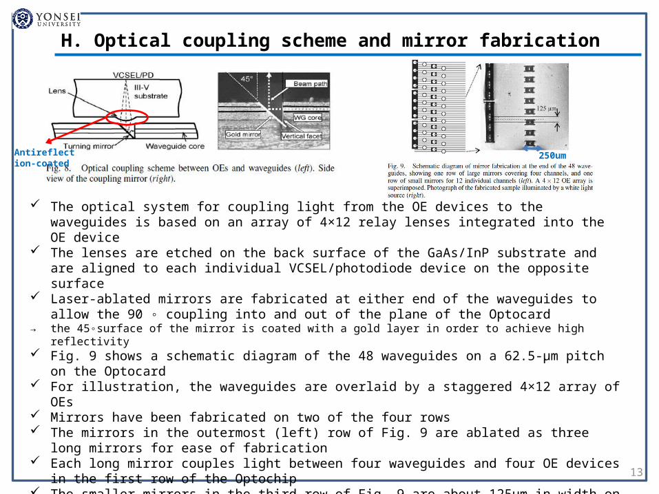
H. Optical coupling scheme and mirror fabrication
13
The optical system for coupling light from the OE devices to the waveguides is based on an array of 4×12 relay lenses integrated into the OE device
The lenses are etched on the back surface of the GaAs/InP substrate and are aligned to each indi-vidual VCSEL/photodiode device on the opposite surface
Laser-ablated mirrors are fabricated at either end of the waveguides to allow the 90 ◦ coupling into and out of the plane of the Optocard
→ the 45◦surface of the mirror is coated with a gold layer in order to achieve high reflectivity Fig. 9 shows a schematic diagram of the 48 waveguides on a 62.5-μm pitch on the Optocard For illustration, the waveguides are overlaid by a staggered 4×12 array of OEs Mirrors have been fabricated on two of the four rows The mirrors in the outermost (left) row of Fig. 9 are ablated as three long mirrors for ease of fabrica-
tion Each long mirror couples light between four waveguides and four OE devices in the first row of the
Optochip The smaller mirrors in the third row of Fig. 9 are about 125μm in width on a 250-μm pitch It can be seen that some light is leaking through the neighboring channels of the illuminated channel
in the large mirrors, owing to the fact that the individual mirrors of row three only partially extend over the neighboring waveguides and allow some light through to the row with the large mirrors
Antireflection-coated
250um
Packaging
14
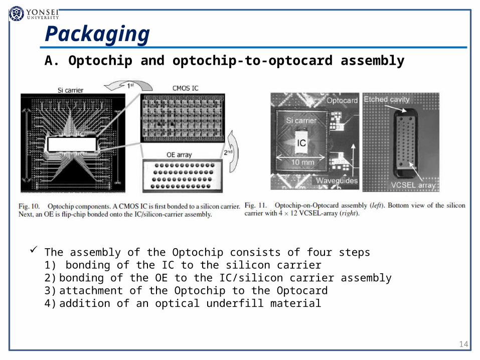
The assembly of the Optochip consists of four steps1) bonding of the IC to the silicon carrier2) bonding of the OE to the IC/silicon carrier assembly3) attachment of the Optochip to the Optocard4) addition of an optical underfill material
A. Optochip and optochip-to-optocard assembly
Packaging
15
Due to the high degree of integration of the Terabus package, thermal chal-lenges arise
high-speed performance and lifetime of VCSELs are strongly temperature sensitive, as is the photodiode leakage
strategy to deal with these issues is threefold1) based on thermal modeling of the full Optochip, the OE devices are optimized for
operation at 70 ◦C at the contact pads2) the ICs are designed for low-power operation, with a total link power consumption
of less than 100 mW per channel being targeted in an initial phase and 50 mW per channel being a more aggressive objective
3) the thermal simulations of the full package suggest that an additional cooling sys-tem able to handle a heat flux of up to 60 W/cm2 is necessary
B. Thermal management
Evaluation and results
16
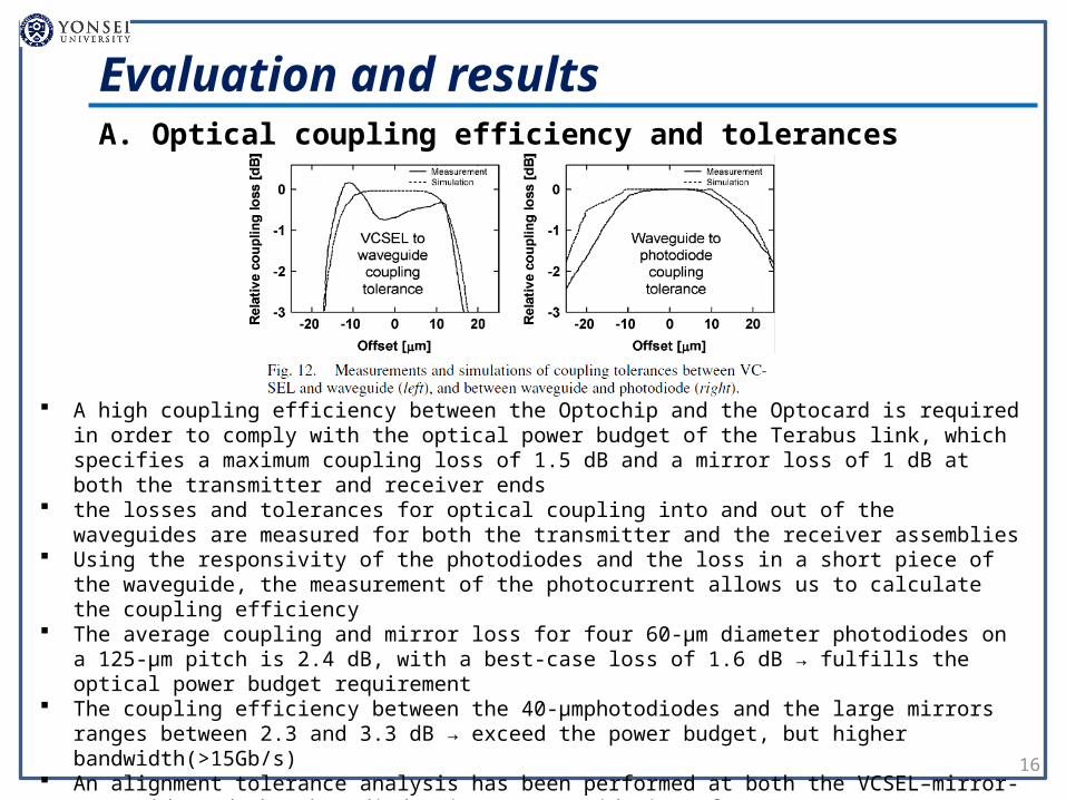
A high coupling efficiency between the Optochip and the Optocard is required in order to comply with the optical power budget of the Terabus link, which specifies a maximum coupling loss of 1.5 dB and a mirror loss of 1 dB at both the transmitter and receiver ends
the losses and tolerances for optical coupling into and out of the waveguides are measured for both the transmitter and the receiver assemblies
Using the responsivity of the photodiodes and the loss in a short piece of the waveguide, the mea-surement of the photocurrent allows us to calculate the coupling efficiency
The average coupling and mirror loss for four 60-μm diameter photodiodes on a 125-μm pitch is 2.4 dB, with a best-case loss of 1.6 dB → fulfills the optical power budget requirement
The coupling efficiency between the 40-μmphotodiodes and the large mirrors ranges between 2.3 and 3.3 dB → exceed the power budget, but higher bandwidth(>15Gb/s)
An alignment tolerance analysis has been performed at both the VCSEL–mirror-waveguide and the photodiode–mirror-waveguide interfaces
The tolerance required for less than 0.7 dB (85%) of change in the coupling efficiency is better than ±13 μm on the VCSEL-side and better than ±14 μm for coupling to the photodiodes of 60-μm diameter
A. Optical coupling efficiency and tolerances
B. Waveguide loss measurements
17
The average loss of the 30-cm waveguides is found to be −4.8 dB, with a best channel loss of −3 dB, corresponding to an average of 0.16 dB/cm and a best-case loss of 0.10 dB/cm
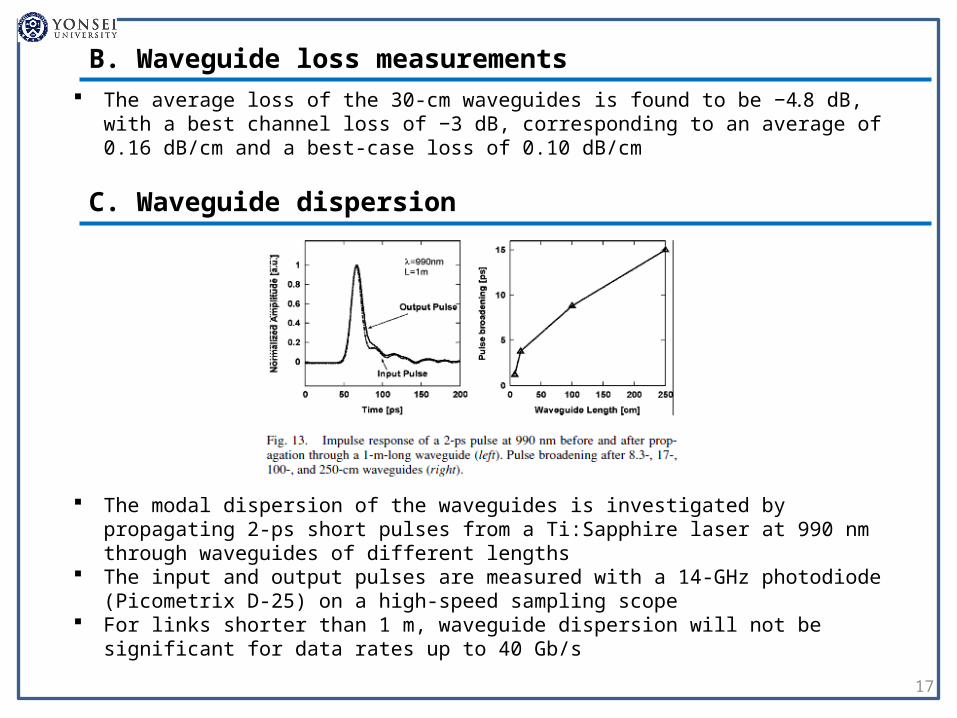
C. Waveguide dispersion
The modal dispersion of the waveguides is investigated by propagating 2-ps short pulses from a Ti:Sapphire laser at 990 nm through waveguides of different lengths
The input and output pulses are measured with a 14-GHz photodiode (Picometrix D-25) on a high-speed sampling scope
For links shorter than 1 m, waveguide dispersion will not be significant for data rates up to 40 Gb/s
D. Electrical signal path
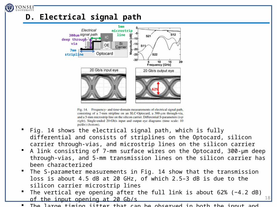
18
Fig. 14 shows the electrical signal path, which is fully differential and consists of striplines on the Optocard, silicon carrier through-vias, and microstrip lines on the silicon carrier
A link consisting of 7-mm surface wires on the Optocard, 300-μm deep through-vias, and 5-mm transmission lines on the silicon carrier has been characterized
The S-parameter measurements in Fig. 14 show that the transmission loss is about 4.5 dB at 20 GHz, of which 2.5–3 dB is due to the silicon carrier microstrip lines
The vertical eye opening after the full link is about 62% (−4.2 dB) of the input opening at 20 Gb/s
The large timing jitter that can be observed in both the input and the output eyes is mostly due to the pattern generator used in these measurements and not due to the interconnect
7mm stripline
5mm microstrip line
300um deep through-via
62%
E. Transmitter optochip
19
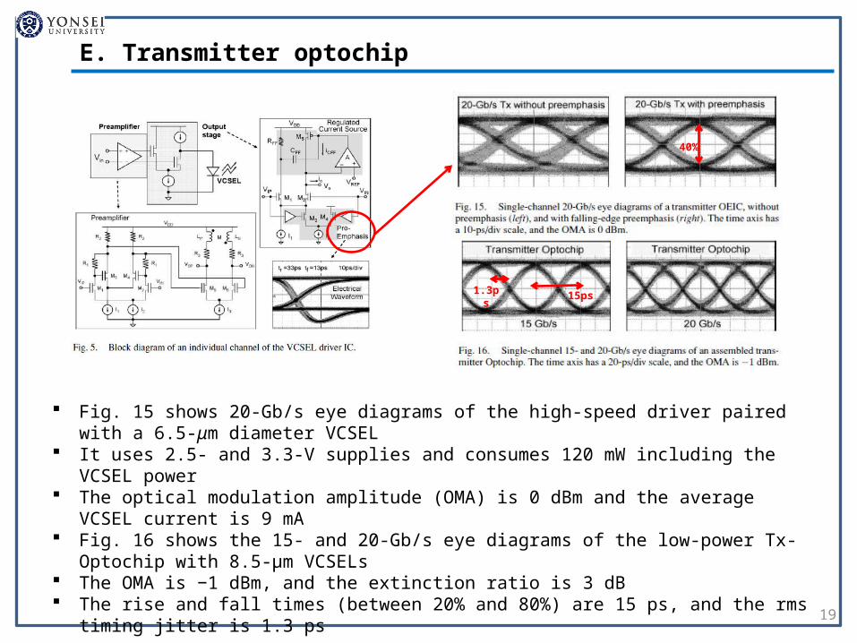
Fig. 15 shows 20-Gb/s eye diagrams of the high-speed driver paired with a 6.5-μm diameter VCSEL
It uses 2.5- and 3.3-V supplies and consumes 120 mW including the VCSEL power The optical modulation amplitude (OMA) is 0 dBm and the average VCSEL current is 9 mA Fig. 16 shows the 15- and 20-Gb/s eye diagrams of the low-power Tx-Optochip with 8.5-μm
VCSELs The OMA is −1 dBm, and the extinction ratio is 3 dB The rise and fall times (between 20% and 80%) are 15 ps, and the rms timing jitter is 1.3 ps
40%
15ps1.3ps
F. Receiver optochip
20
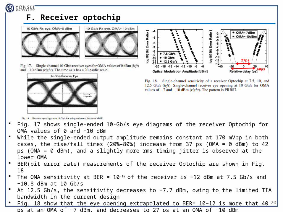
Fig. 17 shows single-ended 10-Gb/s eye diagrams of the receiver Optochip for OMA values of 0 and −10 dBm
While the single-ended output amplitude remains constant at 170 mVpp in both cases, the rise/fall times (20%–80%) increase from 37 ps (OMA = 0 dBm) to 42 ps (OMA = 0 dBm), and a slightly more rms timing jitter is observed at the lower OMA
BER(bit error rate) measurements of the receiver Optochip are shown in Fig. 18 The OMA sensitivity at BER = 10−12 of the receiver is −12 dBm at 7.5 Gb/s and −10.8 dBm at 10 Gb/s At 12.5 Gb/s, the sensitivity decreases to −7.7 dBm, owing to the limited TIA bandwidth in the current de-
sign Fig. 18 show that the eye opening extrapolated to BER= 10−12 is more that 40 ps at an OMA of −7 dBm,
and decreases to 27 ps at an OMA of −10 dBm Fig. 19 shows a 14-Gb/s eye diagram of a receiver Optochip after transmission over a short 5-m MMF
link
40ps
27ps
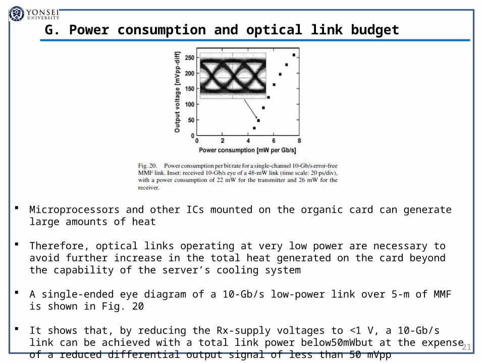
G. Power consumption and optical link budget
21
Microprocessors and other ICs mounted on the organic card can generate large amounts of heat
Therefore, optical links operating at very low power are necessary to avoid further increase in the total heat generated on the card beyond the capability of the server’s cooling system
A single-ended eye diagram of a 10-Gb/s low-power link over 5-m of MMF is shown in Fig. 20
It shows that, by reducing the Rx-supply voltages to <1 V, a 10-Gb/s link can be achieved with a total link power below50mWbut at the expense of a reduced differential output signal of less than 50 mVpp
Conclusion
22
The next phase of Terabus will focus on parallel system-level demonstration of the components developed to date
Terabus is an initial step toward a complete technology for chip-to-chip or board-to-board optical buses
Such systems would permit greater bandwidths between proces-sors or modules in highperformance computer systems
While much additional work needs to be carried out before a complete com-mercial technology becomes realistic, the results summarized earlier are promising and demonstrate that such interconnects are possible