nanotechnology applications to telecommunications and networking (minoli/nanotechnology applications...
TRANSCRIPT
CHAPTER 1
Nanotechnology and Its Business Applications
1.1 INTRODUCTION AND SCOPE
1.1.1 Introduction to the Nanoscale
Nanotechnology is receiving a lot of attention of late across the globe. The termnano originates etymologically from the Greek, and it means “dwarf.” The term indi-cates physical dimensions that are in the range of one-billionth (10�9) of a meter.This scale is called colloquially nanometer scale, or also nanoscale. One nanometeris approximately the length of two hydrogen atoms. Nanotechnology relates to thedesign, creation, and utilization of materials whose constituent structures exist at thenanoscale; these constituent structures can, by convention, be up to 100 nm in size.1–3
Nanotechnology is a growing field that explores electrical, optical, and magneticactivity as well as structural behavior at the molecular and submolecular level. Oneof the practical applications of nanotechnology (but certainly not the only one) is thescience of constructing computer chips and other devices using nanoscale buildingelements. This book is a basic practical survey of this field with an eye on comput-ing and telecom applications.
The nanoscale dimension is important because quantum mechanical (non-Newtonian) properties of electronics, photons, and atoms are evident at this scale.Nanoscale structures permit the control of fundamental properties of materials withoutchanging the materials’ chemical status. Nanostructure, such as nanophotonic devices,nanowires, carbon nanotubes, plasmonics devices, among others, are planned to be
1
Nanotechnology Applications to Telecommunications and Networking, By Daniel MinoliCopyright © 2006 John Wiley & Sons, Inc.
1Measures are relatives; hence, one can talk about something being 1000 nanometers (nm), or 1 microm(µm), of 10,000 Angstroms (Å). A micron is a unit of measurement representing one-millionth of a meterand is equivalent to a micrometer. An angstrom is a unit of measurement indicating one-tenth of ananometer, or one ten-billionth of a meter (often used in physics and/optics to measure atoms and wave-lengths of light).2Atoms are typically between 0.1 and 0.5 nm wide.3For comparison, a human hair is between 100,000 and 200,000 nm in diameter and a virus is typically100 nm wide.
Minoli_ch01.qxd 9/27/2005 8:49 AM Page 1
incorporated into telecommunication components and into microprocessors in thenext few years, leading to more powerful communication systems and computers—these nanostructures are discussed in the chapters that follow. Nanotechnology isseen as a high-profile emerging area of science and technology. Proponents prog-nosticate that, in the next few years, nanotechnology will have a major impact onsociety. Recently, Charles Vest [1], the president of MIT, observed: “The gatheringnanotechnology revolution will eventually make possible a huge leap in computingpower, vastly stronger yet much lighter materials, advances in medical technologies,as well as devices and processes with much lower energy and environmental costs.”There already are an estimated 20,000 researchers worldwide working in nanotech-nology today.
In the sections that follow in this chapter we preliminarily answer questions suchas: What is nanotechnology? What are the applications of nanotechnology? What isthe market potential for nanotechnology? What are the global research activities innanotechnology? Why would a practitioner (the likely reader of this book), need tocare? We then position the reader for the balance of the book, which looks at the nan-otechnology topic from an application, and, more specifically, from a telecom- andnetworking-perspective angle.
While many definitions for nanotechnology exist, the National NanotechnologyInitiative (NNI4), calls an area of research, development, and engineering “nano-technology” only if it involves all of the following [2]:
1. Research and technology development at the atomic, molecular, or macromol-ecular levels, in the length scale of approximately 1- to 100-nm range
2. Creating and using structures, devices, and systems that have novel propertiesand functions because of their small and/or intermediate size
3. Ability to control or manipulate matter on the atomic scale
Hence, nanotechnology can be defined as the ability to work at the molecularlevel, atom by atom, to create large structures with fundamentally new properties andfunctions. Nanotechnology can be described as the precision-creation and precision-manipulation of atomic-scale matter [3]; hence, it is also referred to as precisionmolecular engineering. Nanotechnology is the application of nanoscience to controlprocesses on the nanometer scale, that is, between 0.1 and 100 nm [4]. The field isalso known as molecular engineering or molecular nanotechnology (MNT). MNTdeals with the control of the structure of matter based on atom-by-atom and/ormolecule-by-molecule engineering; also, it deals with the products and processes ofmolecular manufacturing [5]. The term engineered nanoparticles describes particlesthat do not occur naturally; humans have been putting together different materialsthroughout time, and now with nanotechnology they are doing so at the nanoscale.
2 NANOTECHNOLOGY AND ITS BUSINESS APPLICATIONS
4The National Nanotechnology Initiative (NNI) is a U.S. government-funded R&D and commercializa-tion initiative for nanoscience and nanotechnology. The 21st Century Nanotechnology Research andDevelopment Act of 2003 put into law programs and activities supported by the initiative.
Minoli_ch01.qxd 9/27/2005 8:49 AM Page 2
As it might be inferred, nanotechnology is highly interdisciplinary as a field, and itrequires knowledge drawn from a variety of scientific and engineering arenas:Designing at the nanoscale is working in a world where physics, chemistry, electri-cal engineering, mechanical engineering, and even biology become unified into anintegrated field. “Building blocks” for nanomaterials include carbon-based compo-nents and organics, semiconductors, metals, and metal oxides; nanomaterials are theinfrastructure, or building blocks, for nanotechnology.
The term nanotechnology was introduced by Nori Taniguchi in 1974 at the TokyoInternational Conference on Production Engineering. He used the word to describeultrafine machining: the processing of a material to nanoscale precision. This workwas focused on studying the mechanisms of machining hard and brittle materialssuch as quartz crystals, silicon, and alumina ceramics by ultrasonic machining. Yearsearlier, in a lecture at the annual meeting of the American Physical Society in 1959(There’s Plenty of Room at the Bottom) American Physicist and Nobel LaureateRichard Feynman argued (although he did not coin or use the word nanotechnology)that the scanning electron microscope could be improved in resolution and stability,so that one would be able to “see” atoms. Feynman proceeded to predict the abilityto arrange atoms the way a researcher would want them, within the bounds of chem-ical stability, in order to build tiny structures that in turn would lead to molecular oratomic synthesis of materials [6]. Based on Feynman’s idea, K. E. Drexler advancedthe idea of “molecular nanotechnology” in 1986 in the book Engines of Creation,where he postulated the concept of using nanoscale molecular structures to act in amachinelike manner to guide and activate the synthesis of larger molecules. Drexlerproposed the use of a large number (billions) of roboticlike machines called “assem-blers” (or nanobots) that would form the basis of a molecular manufacturing tech-nology capable of building literally anything atom by atom and molecule bymolecule. Quite a bit of work has been done in the field since the publication of thebook, although the concept of nanobots is still speculative.5
At this time, an engineering discipline has already grown out of the pure andapplied science; however, nanoscience still remains somewhat of a maturing field.Nanotechnology can be identified precisely with the concept of “molecular manu-facturing” (molecular nanotechnology) introduced above or with a broader definitionthat also includes laterally related subdisciplines [7]. This text will encompass bothperspectives; the context should make clear which of the definitions we are using.The nanoscale is where physical and biological systems approach a comparabledimensional scale. A basic “difference” between systems biology and nanotechnol-ogy is the goal of the science: systems biology aims to uncover the fundamentaloperation of the cell in an effort to predict the exact response to specific stimuli andgenetic variations (has scientific discovery focus); nanotechnology, on the otherhand, does not attempt to be so precise but is chiefly concerned with useful design
INTRODUCTION AND SCOPE 3
5The possibility of building tiny motors on the scale of a molecule appears to have been brought onestep closer of late: researchers recently have described how they were able—using light or electricalstimulation—to cause a molecule to rotate on an axis in a controlled fashion, similar to the action of amotor [8].
Minoli_ch01.qxd 9/27/2005 8:49 AM Page 3
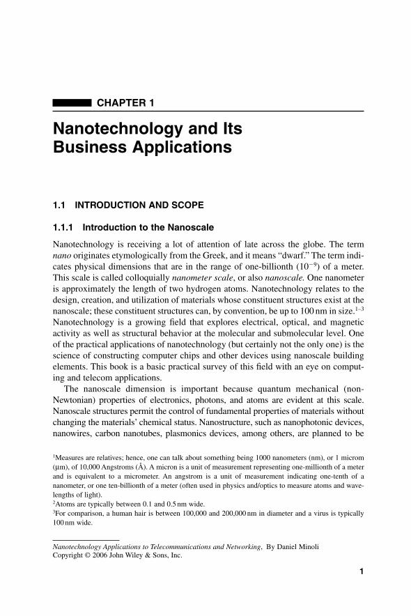
(has engineering design focus) [9]. Figure 1.1 depicts the current evolution of vari-ous disciplines toward a nanoscale focus.
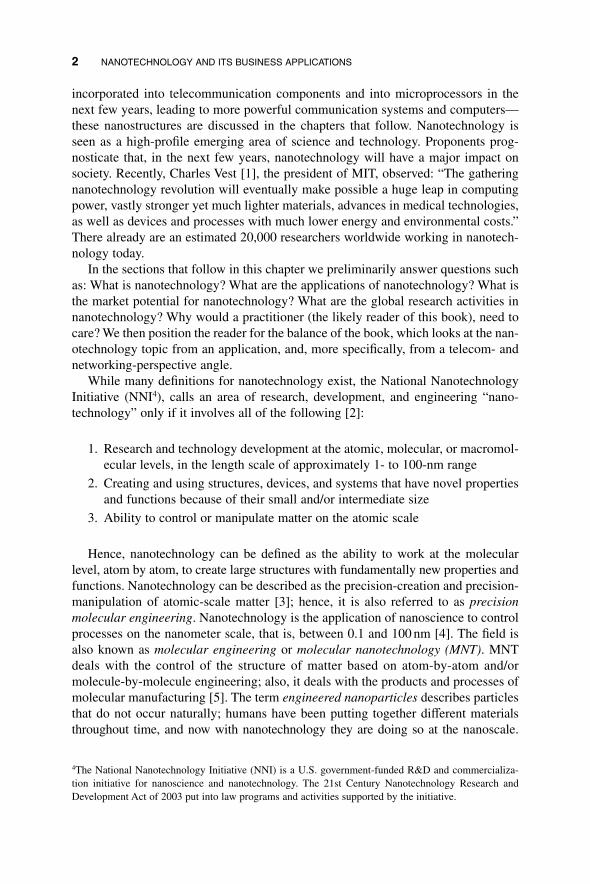
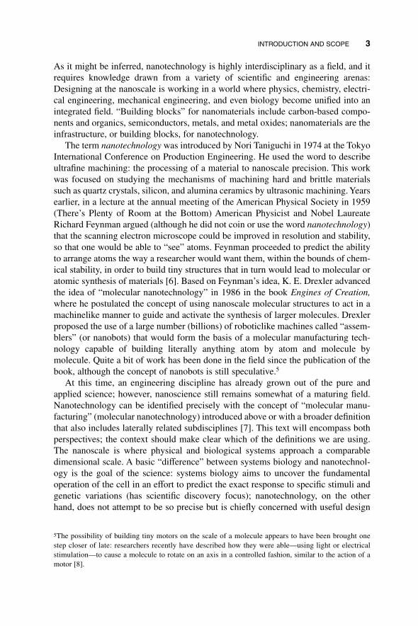
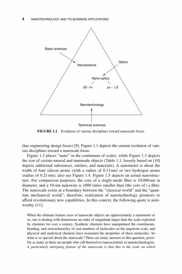
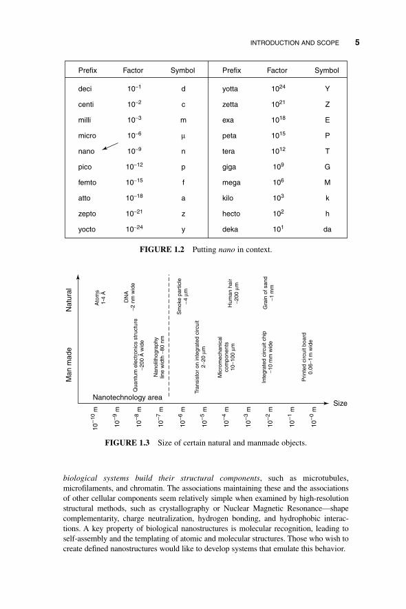
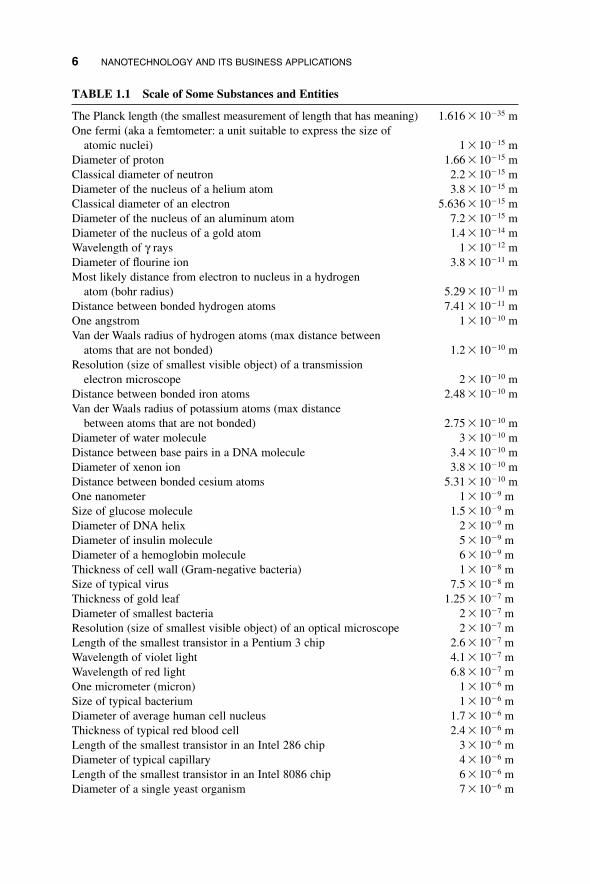
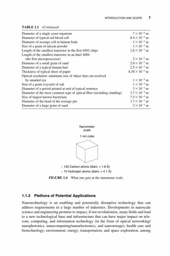
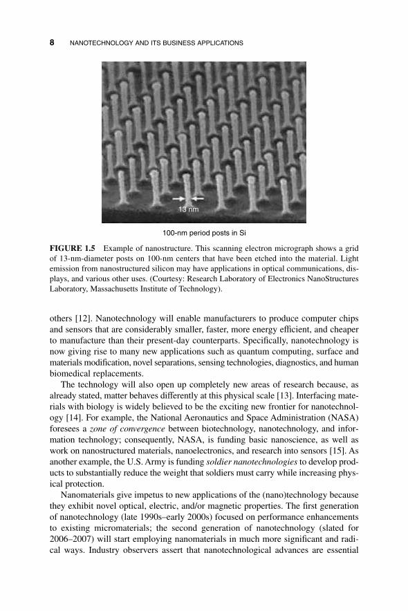
Figure 1.2 places “nano” in the continuum of scales, while Figure 1.3 depictsthe size of certain natural and manmade objects (Table 1.1, loosely based on [10]depicts additional substances, entities, and materials). A nanometer is about thewidth of four silicon atoms (with a radius of 0.13 nm) or two hydrogen atoms(radius of 0.21 nm); also see Figure 1.4. Figure 1.5 depicts an actual nanostruc-ture. For comparison purposes, the core of a single-mode fiber is 10,000 nm indiameter, and a 10-nm nanowire is 1000 times smaller than (the core of ) a fiber.The nanoscale exists at a boundary between the “classical world” and the “quan-tum mechanical world”; therefore, realization of nanotechnology promises toafford revolutionary new capabilities. In this context, the following quote is note-worthy [11]:
When the ultimate feature sizes of nanoscale objects are approximately a nanometer orso, one is dealing with dimensions an order of magnitude larger than the scale exploitedby chemists for over a century. Synthetic chemists have manipulated the constituents,bonding, and stereochemistry of vast numbers of molecules on the angstrom scale, andphysical and analytical chemists have examined the properties of these molecules. Sowhat is so special about the nanoscale? There are many answers to this question, possi-bly as many as there are people who call themselves nanoscientists or nanotechnologists.A particularly intriguing feature of the nanoscale is that this is the scale on which
4 NANOTECHNOLOGY AND ITS BUSINESS APPLICATIONS
Basic sciences
Nanoscience
Nano-optics
Nanotechnology
∆x ~ � /2∆E~ h�
Technical sciences
Optics
FIGURE 1.1 Evolution of various disciplines toward nanoscale focus.
Minoli_ch01.qxd 9/27/2005 8:49 AM Page 4
INTRODUCTION AND SCOPE 5
Prefix
deci 10−1
centi 10−2
milli 10−3
micro 10−6
nano 10−9
pico 10−12
femto 10−15
atto 10−18
zepto 10−21
yocto
d
c
m
µ
n
p
f
a
z
y10−24
Factor Symbol Prefix
yotta 1024
zetta 1021
exa 1018
peta 1015
tera 1012
giga 109
mega 106
kilo 103
hecto 102
deka
Y
Z
E
P
T
G
M
k
h
da101
Factor Symbol
FIGURE 1.2 Putting nano in context.
Man
mad
e
Size
Nat
ural
Nanotechnology area
10− 1
0 m
10− 9
m
10−8
m
10−7
m
10−6
m
10−5
m
10−4
m
10−3
m
10− 2
m
10−1
m
10− 0
m
Ato
ms
1-4
A
DN
A−2
nm
wid
eQ
uant
um e
lect
roni
cs s
truc
ture
−200
A w
ide
Nan
olith
ogra
phy
line
wid
th −
80 n
m
Sm
oke
part
icle
−4 µ
m
Tran
sist
or o
n in
tegr
ated
circ
uit
2−20
µm
Mic
rom
echa
nica
lco
mpo
nent
s10
−100
µm
Hum
an h
air
−200
µm
Gra
in o
f san
d−1
mm
Inte
grat
ed c
ircui
t chi
p−1
0m
m w
ide
Prin
ted
circ
uit b
oard
0.06
−1m
wid
e
°
°
FIGURE 1.3 Size of certain natural and manmade objects.
biological systems build their structural components, such as microtubules,microfilaments, and chromatin. The associations maintaining these and the associationsof other cellular components seem relatively simple when examined by high-resolutionstructural methods, such as crystallography or Nuclear Magnetic Resonance—shapecomplementarity, charge neutralization, hydrogen bonding, and hydrophobic interac-tions. A key property of biological nanostructures is molecular recognition, leading toself-assembly and the templating of atomic and molecular structures. Those who wish tocreate defined nanostructures would like to develop systems that emulate this behavior.
Minoli_ch01.qxd 9/27/2005 8:49 AM Page 5
6 NANOTECHNOLOGY AND ITS BUSINESS APPLICATIONS
TABLE 1.1 Scale of Some Substances and Entities
The Planck length (the smallest measurement of length that has meaning) 1.616 � 10�35 mOne fermi (aka a femtometer: a unit suitable to express the size of
atomic nuclei) 1 � 10�15 mDiameter of proton 1.66 � 10�15 mClassical diameter of neutron 2.2 � 10�15 mDiameter of the nucleus of a helium atom 3.8 � 10�15 mClassical diameter of an electron 5.636 � 10�15 mDiameter of the nucleus of an aluminum atom 7.2 � 10�15 mDiameter of the nucleus of a gold atom 1.4 � 10�14 mWavelength of γ rays 1 � 10�12 mDiameter of flourine ion 3.8 � 10�11 mMost likely distance from electron to nucleus in a hydrogen
atom (bohr radius) 5.29 � 10�11 mDistance between bonded hydrogen atoms 7.41 � 10�11 mOne angstrom 1 � 10�10 mVan der Waals radius of hydrogen atoms (max distance between
atoms that are not bonded) 1.2 � 10�10 mResolution (size of smallest visible object) of a transmission
electron microscope 2 � 10�10 mDistance between bonded iron atoms 2.48 � 10�10 mVan der Waals radius of potassium atoms (max distance
between atoms that are not bonded) 2.75 � 10�10 mDiameter of water molecule 3 � 10�10 mDistance between base pairs in a DNA molecule 3.4 � 10�10 mDiameter of xenon ion 3.8 � 10�10 mDistance between bonded cesium atoms 5.31 � 10�10 mOne nanometer 1 � 10�9 mSize of glucose molecule 1.5 � 10�9 mDiameter of DNA helix 2 � 10�9 mDiameter of insulin molecule 5 � 10�9 mDiameter of a hemoglobin molecule 6 � 10�9 mThickness of cell wall (Gram-negative bacteria) 1 � 10�8 mSize of typical virus 7.5 � 10�8 mThickness of gold leaf 1.25 � 10�7 mDiameter of smallest bacteria 2 � 10�7 mResolution (size of smallest visible object) of an optical microscope 2 � 10�7 mLength of the smallest transistor in a Pentium 3 chip 2.6 � 10�7 mWavelength of violet light 4.1 � 10�7 mWavelength of red light 6.8 � 10�7 mOne micrometer (micron) 1 � 10�6 mSize of typical bacterium 1 � 10�6 mDiameter of average human cell nucleus 1.7 � 10�6 mThickness of typical red blood cell 2.4 � 10�6 mLength of the smallest transistor in an Intel 286 chip 3 � 10�6 mDiameter of typical capillary 4 � 10�6 mLength of the smallest transistor in an Intel 8086 chip 6 � 10�6 mDiameter of a single yeast organism 7 � 10�6 m
Minoli_ch01.qxd 9/27/2005 8:49 AM Page 6
INTRODUCTION AND SCOPE 7
TABLE 1.1 (Continued)
Diameter of a single yeast organism 7 � 10�6 mDiameter of typical red blood cell 8.4 � 10�6 mDiameter of average cell in human body 1 � 10�5 mSize of a grain of talcum powder 1 � 10�5 mLength of the smallest transistor in the first 6502 chips 1.6 � 10�5 mLength of the smallest transistor in an Intel 4004
(the first microprocessor) 2 � 10�5 mDiameter of a small grain of sand 2.0 � 10�5 mDiameter of a typical human hair 2.5 � 10�5 mThickness of typical sheet of paper 8.38 � 10�5 mOptical resolution: minimum size of object that can resolved
by unaided eye 1 � 10�4 mSize of a grain (crystal) of salt 1 � 10�4 mDiameter of a period printed at end of typical sentence 3 � 10�4 mDiameter of the most common type of optical fiber (including cladding) 3.7 � 10�4 mSize of largest known bacterium 7.5 � 10�4 mDiameter of the head of the average pin 1.7 � 10�3 mDiameter of a large grain of sand 2 � 10�3 m
~ 125 Carbon atoms (diam. = 1.8 A)
Nanometerscale
1 nm cube
~ 15 Hydrogen atoms (diam. = 4.1 A)
°
°
FIGURE 1.4 What one gets at the nanometer scale.
1.1.2 Plethora of Potential Applications
Nanotechnology is an enabling and potentially disruptive technology that canaddress requirements in a large number of industries. Developments in nanoscalescience and engineering promise to impact, if not revolutionize, many fields and leadto a new technological base and infrastructure that can have major impact on tele-com, computing, and information technology (in the form of optical networking/nanophotonics, nanocomputing/nanoelectronics, and nanostorage); health care andbiotechnology; environment; energy; transportation; and space exploration, among
Minoli_ch01.qxd 9/27/2005 8:49 AM Page 7
others [12]. Nanotechnology will enable manufacturers to produce computer chipsand sensors that are considerably smaller, faster, more energy efficient, and cheaperto manufacture than their present-day counterparts. Specifically, nanotechnology isnow giving rise to many new applications such as quantum computing, surface andmaterials modification, novel separations, sensing technologies, diagnostics, and humanbiomedical replacements.
The technology will also open up completely new areas of research because, asalready stated, matter behaves differently at this physical scale [13]. Interfacing mate-rials with biology is widely believed to be the exciting new frontier for nanotechnol-ogy [14]. For example, the National Aeronautics and Space Administration (NASA)foresees a zone of convergence between biotechnology, nanotechnology, and infor-mation technology; consequently, NASA, is funding basic nanoscience, as well aswork on nanostructured materials, nanoelectronics, and research into sensors [15]. Asanother example, the U.S. Army is funding soldier nanotechnologies to develop prod-ucts to substantially reduce the weight that soldiers must carry while increasing phys-ical protection.
Nanomaterials give impetus to new applications of the (nano)technology becausethey exhibit novel optical, electric, and/or magnetic properties. The first generationof nanotechnology (late 1990s–early 2000s) focused on performance enhancementsto existing micromaterials; the second generation of nanotechnology (slated for2006–2007) will start employing nanomaterials in much more significant and radi-cal ways. Industry observers assert that nanotechnological advances are essential
8 NANOTECHNOLOGY AND ITS BUSINESS APPLICATIONS
13 nm
100-nm period posts in Si
FIGURE 1.5 Example of nanostructure. This scanning electron micrograph shows a gridof 13-nm-diameter posts on 100-nm centers that have been etched into the material. Lightemission from nanostructured silicon may have applications in optical communications, dis-plays, and various other uses. (Courtesy: Research Laboratory of Electronics NanoStructuresLaboratory, Massachusetts Institute of Technology).
Minoli_ch01.qxd 9/27/2005 8:49 AM Page 8

if one is to continue the revolution in computer hardware beyond about the nextdecade; furthermore, nanotechnology will also allow us to fabricate an entire newgeneration of products that are cleaner, stronger, lighter, and more precise6 [7].Nanomaterials with structural features at the nanoscale can be found in the form ofclusters, thin films, multilayers, and nanocrystalline materials often expressed by thedimensionality of 0, 1, 2 and 3; the materials of interest include metals, amorphousand crystalline alloys, semiconductors, oxides, nitride and carbide ceramics in theform of clusters, thin films, multilayers, and bulk nanocrystalline materials [16].
All products are manufactured from atoms, however, interestingly, the propertiesof those products depend on how those atoms are arranged. For example, by rear-ranging the atoms in coal (carbon), one can make diamonds. It should be noted thatcurrent manufacturing techniques are very rudimentary at the atomic/molecularlevel: casting, grinding, milling, and even lithography move atoms in bulk ratherthan in a “choreographed” or “highly controlled” fashion. On the other hand, withnanotechnology one is able to assemble the fundamental building blocks of nature(atoms, molecules, etc.), within the constraints of the laws of physics, but in waysthat may not occur naturally or in ways to create some existing structure but by syn-thesizing it out of cheaper forms or constituent elements. Nanomaterials often haveproperties dramatically different from their bulk-scale counterparts; for example,nanocrystalline copper is five times harder than ordinary copper with its microme-ter-sized crystalline structure [17]. A goal of nanotechnology is to close the size gapbetween the smallest lithographically fabricated structures and chemically synthe-sized large molecules [18].
As scientists and engineers continue to push forward the limits of computer chipmanufacturing, they have entered into the nanometer realm in recent years withoutmuch public fanfare: The first transistor gates under 100 nm went into production in2000, and microprocessor chips that were coming to market at press time had gates45 nm wide [19]. A Pentium 4 chip contains in the range of 50 million transistors.However, as the physical laws related to today’s telecom chipsets, computer memory,and processor fabrication reach their limits, new approaches such as single-electrontechnology (nanoelectronics) or plasmonics (nanophotonics) are needed. The inven-tion of the scanning tunneling microscope, the discovery of the fullerene family ofmolecules, the development of materials with size-dependent properties, and the abil-ity to encode with and manipulate biological molecules such as deoxyribonucleic acid(DNA), are a few of the crucial developments that have advanced nanotechnology inthe recent past [20]. A gamut of products featuring the unique properties of nanoscalematerials are already available to consumers and industry at this time. For example,most computer hard drives contain giant magnetoresistance (GMR) heads that,through nanothin layers of magnetic materials, allow for a significant increase instorage capacity. Other electronic applications include nonvolatile magnetic memory,automotive sensors, landmine detectors, and solid-state compasses. Some other
INTRODUCTION AND SCOPE 9
6It is worth noting that the National Science Foundation has estimated that 2 million workers will beneeded to support nanotechnology industries worldwide within 15 years.
Minoli_ch01.qxd 9/27/2005 8:49 AM Page 9
nanotechnology uses that are already in the marketplace include (also see Table 1.2[2] and Table 1.3 [21]):
• Burn and wound dressings
• Water filtration
• Catalysis
• A dental-bonding agent
• Coatings for easier cleaning glass
• Bumpers and catalytic converters on cars
• Protective and glare-reducing coatings for eyeglasses and cars
• Sunscreens and cosmetics
• Longer-lasting tennis balls
10 NANOTECHNOLOGY AND ITS BUSINESS APPLICATIONS
TABLE 1.2 Recent Achievements in Nanotechnology (Partial List)
Use of the bright fluorescence of semiconductor nanocrystals for dynamic angiographyin capillaries hundreds of micrometers below the skin of living mice—about twice thedepth of conventional angiographic materials—and obtained with one-fifth theirradiation power.
Nanoelectromechanical sensors that can detect and identify a single molecule of a chemicalwarfare agent—an essential step toward realizing practical field sensors.
Nanotube-based fibers requiring 3 times the energy to break of the strongest silk fibers and15 times that of Kevlar fiber.
Nanocomposite energetic materials for propellants and explosives that have over twice theenergy output of typical high explosives.
Prototype data storage devices based on molecular electronics with data densities over 100times that of today’s highest density commercial devices.
Field demonstration that iron nanoparticles can remove up to 96% of a major contaminant(trichloroethylene) from groundwater at an industrial site.
TABLE 1.3 Short-Term Commercially Viable Nanotechnology Products
Examples of Products Generating Sector Revenues in 2005 and Beyond
Building materials Scratchless long endurance treatments for vinyl,roofing, furniture, etc.; self-cleaning windows
Communications and computers Nanodrives and memory, enhanced displays and electronic paper, copiers and printers; sensors as inputs for security and monitoring systems
Military and aerospace Materials and coatings for hardening products; sensorsChemicals Advanced catalysts and additivesPharmaceuticals and medical Better targeted pharmaceuticals and cosmetics; drug
devices delivery systems; nanobiotechnology productsEnergy Filters, additives, and catalysts for hydrocarbon-based
fuels; photovoltaics
Minoli_ch01.qxd 9/27/2005 8:49 AM Page 10
• Light-weight, stronger tennis racquets
• Stain-free clothing and mattresses
• Ink
Telecommunications- and computing-specific applications include, among others:
• Nanoelectronics, nanophotonics, nanomaterials, new chipsets
• Optical transmission [e.g., in the emerging optical transport network (OTN)]
• Optical switching [e.g., in the emerging automatically switched optical network(ASON)]
• Microelectromechanical systems (MEMS) and microoptical-electromechanicalsystems (MOEMS) applications [e.g., tunable optical components and modules,optical switches, fiber-optic networks, electromagnetic radio frequency (RF)MEMS switch; sensor; actuators; information storage systems including mag-netic recording, optical recording, and other recording devices, e.g., rigid disk,flexible disk, tape and card drives; processing systems including copiers, print-ers, scanners, and digital cameras]
• Speech recognition/pattern recognition/imaging
• Advanced computing (e.g., quantum computing, pervasive computing, ubiquitouscomputing, autonomic computing, utility computing, grid computing, molecularcomputing, massively parallel computing, and amorphous computing)
• Storage
• “Terascale integration” microprocessors
• Quantum cryptography
• Nanosensors and nanoactuators
Focusing on electronics and photonics, note that the micrometer (10�6 m) range isrepresentative of typical computing technology of the late 1990s–early 2000s: random-access memory (RAM), read-only memory (ROM), and microprocessors have fea-ture sizes on the order of micrometers. The entire advancement of processor technologyand (optical) communication is essentially the effort to shrink circuits from microm-eters down to fractions of a micrometer (e.g., 0.1 µm or less). Silicon can bemachined into slabs 0.3–0.1 µm wide (this is smaller than the wavelength of deepviolet light). This is what one could do at press time with conventional processingtechnology. Somewhere between 0.5 and 0.1 µm some of the basic laws (such asOhm’s law) begin to break down, and the rules of quantum theory begin to becomeimportant if not overriding [5].
Consider for illustrative purposes one example of nanoelectronic (nano)structures,specifically nanowires. Nanowires are electrical conductors that function like wiresbut exist at the nanoscale. Nanowires can be used to manufacture faster computerchips, higher-density memory, and smaller lasers. Nanowires are molecular struc-tures with characteristic electrical or optical properties. They are one of the key com-ponents to be used for the creation of “molecular electronics chips.” These wireshave been manufactured in the 40- to 80-nm-diameter range. Nanowires are relatively
INTRODUCTION AND SCOPE 11
Minoli_ch01.qxd 9/27/2005 8:49 AM Page 11
easy to produce, and they can be assembled in grids to become the basis of nanoscalelogic circuits. Nanowires can have a number of (very) different shapes: They oftenare thin and short “threads” but also have other shapes.
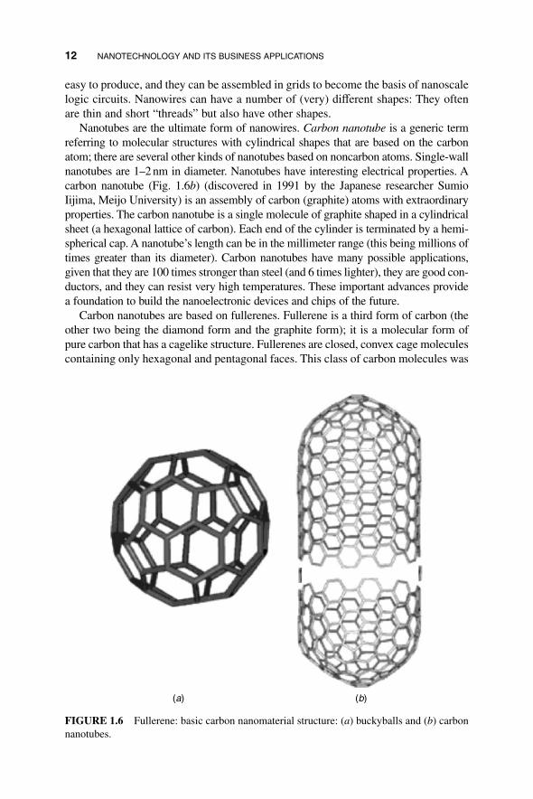
Nanotubes are the ultimate form of nanowires. Carbon nanotube is a generic termreferring to molecular structures with cylindrical shapes that are based on the carbonatom; there are several other kinds of nanotubes based on noncarbon atoms. Single-wallnanotubes are 1–2 nm in diameter. Nanotubes have interesting electrical properties. Acarbon nanotube (Fig. 1.6b) (discovered in 1991 by the Japanese researcher SumioIijima, Meijo University) is an assembly of carbon (graphite) atoms with extraordinaryproperties. The carbon nanotube is a single molecule of graphite shaped in a cylindricalsheet (a hexagonal lattice of carbon). Each end of the cylinder is terminated by a hemi-spherical cap. A nanotube’s length can be in the millimeter range (this being millions oftimes greater than its diameter). Carbon nanotubes have many possible applications,given that they are 100 times stronger than steel (and 6 times lighter), they are good con-ductors, and they can resist very high temperatures. These important advances providea foundation to build the nanoelectronic devices and chips of the future.
Carbon nanotubes are based on fullerenes. Fullerene is a third form of carbon (theother two being the diamond form and the graphite form); it is a molecular form ofpure carbon that has a cagelike structure. Fullerenes are closed, convex cage moleculescontaining only hexagonal and pentagonal faces. This class of carbon molecules was
12 NANOTECHNOLOGY AND ITS BUSINESS APPLICATIONS
(b)(a)
FIGURE 1.6 Fullerene: basic carbon nanomaterial structure: (a) buckyballs and (b) carbonnanotubes.
Minoli_ch01.qxd 9/27/2005 8:49 AM Page 12
discovered by Richard Smalley in 1985. The fullerene structure can be spherical ortubular in shape, as shown in Figure 1.6 (this form of carbon is named in honor ofthe architect Buckminster Fuller, who designed the geodesic structures that thefullerene resembles7). Fullerenes are formed when vaporized carbon condenses in anatmosphere of inert gas. Fullerenes enjoy extraordinary properties, such as supercon-ducting. Buckyballs are the most famous fullerene molecules (pictorially they are closeto the shape of an European soccer ball.) The buckminsterfullerene (buckyball C60)(Fig. 1.6b) is a nanostructure composed of 60 atoms of carbon, organized in a perfectlysymmetric closed cage; much larger fullerenes also exist as seen in Figure 1.6.
1.1.3 Challenges and Opportunities
In 2004 the semiconductor industry reliably crossed the 100-nm fabrication barrier,and manufacturers were able to place 100 million transistors on a chip, but from 2005onward, major challenges were expected to begin to materialize, according to observers.Continued improvements in lithography have resulted in integrated circuits (ICs) withlinewidths that are less than 1 µm (1000 nm): This work is often called “nanotechnology,”especially if/when the 100-nm barrier is crossed.8 However, the challenge arises whenscientists seek to create structures less than 100 nm in two or three dimensions [22].Submicron lithography is a useful technique, but it is equally clear that conventionallithography will not permit the building of semiconductor devices in which individualdopant atoms are located at specific lattice sites: Many of the exponentially improvingtrends in computer hardware capability have remained operative for the last 50 years, andthere is fairly widespread belief that these trends are likely to continue for a number ofyears, but thereafter conventional lithography will start to reach its limits [7].
There are challenges in the area of the gate dielectric, gate electrodes, substrate anddevice structure, and device interconnects [23]. Specifically, (i) there are the powerimplications of Moore’s law9; (ii) two major gaps in the EDA (electronic designautomation) chain, at the architectural and the physical levels; and, (iii) the deep-sub-micron physical effects that jeopardize the separation of design and manufacturing [24].To continue to follow (and/or exceed) the performance goals of Moore’s law, one needsto develop new manufacturing techniques and approaches that will let one build com-puter systems with “mole quantities” of logic elements that are molecular in both sizeand precision and are interconnected in complex patterns, in an inexpensive manner [7].
INTRODUCTION AND SCOPE 13
7American architect Richard Buckminster Fuller designed a dome presenting this kind of symmetric pat-tern for the 1967 Montreal World Exhibition.8For example, in early 2004 Intel announced the first lot of chips based on the 65-nm process: Itannounced the first fully functional 4-Mbit SRAM chips (static random access memory). Intel was plan-ning mass production for 2005. In early 2002, Intel demonstrated prototypes of first SRAM chips basedon the 90-nm process. At that time this was a technological breakthrough; but at press time the 90 nm iswell in reach, with many chip makers releasing such chips [24a].9Gordon Moore made his well-known observation (now known as Moore’s law) in 1965, just a few yearsafter the first ICs were developed. In his original paper Moore observed an exponential growth in the num-ber of transistors per integrated circuit and predicted that this trend would continue. Through technologyadvances, Moore’s law, the doubling of transistors every couple of years, has been maintained and still holdstrue today. Observers (such as Intel) expect that it will continue at least through the end of this decade [25].
Minoli_ch01.qxd 9/27/2005 8:49 AM Page 13
The silicon transistor, as embodied in the complementary metal oxide semicon-ductor (CMOS), is the dominant technology and will likely remain so for the fore-seeable future; only a breakdown in Moore’s law provides a chance for othertechnologies, including nanotechnology, to compete. However, such a break is morelikely to be the result of economics rather than technological problems, according tosome [26]. Nanoelectronics and nanophotonics are of particular interest in this con-text. Contemporary nanotechnology research is concerned, at the macrolevel, withtwo avenues of research: (i) the development of new manufacturing techniques and(ii) the development of new devices, for example, single-electron transistors, nano-wires, and photonic bandgap devices (to mention only a few).
Manufacturing techniques for growing and fabricating structures with dimen-sions as small as a few nanometers using electron beam lithography, dry etching, andmolecular beam epitaxial growth are under development. Novel techniques of man-ufacturing nanometer-scale structures by stamping are also under development. Recentaccomplishments have included the first demonstration of 3-nm electron beamlithography and the invention of new low-damage dry etch processes for selectiveand unselective patterning of the Ga(Al, In)As and InP systems [27].
In reference to new devices, research work in this arena goes on in earnest. Forexample, a baseline 2001 paper for nanoelectronic circuit design demonstrated thatall of the important logic functions for building complex circuits can be built from abottom-up assembly process of chemically synthesized nanowires [28] and/or nan-otubes. As far back as 2001, a team at Nanosys Incorporated (Cambridge, MA)arranged nanowires into a simple crossbar architecture that allowed communicationamong nanowires; the team constructed logic circuits from silicon and galliumnitride nanowires. A team at UCLA demonstrated more recently that a simple 16-bitmemory circuit could be built from semiconducting crossbars that took advantage ofchemical transistor switches made from organically synthesized molecules [29].Advancements like these and other nanotechnology-driven developments will playan important role in the future of telecommunications.
Major opportunities exist for the development of new usable technologies duringthe next few years. As stated earlier, nanostructure, such as nanophotonic devices,nanowires, carbon nanotubes, plasmonics devices, among others, are being devel-oped to the point where these devices can be incorporated into telecommunicationcomponents and into microprocessors, leading to powerful new communication sys-tems and computers. These opportunities will be described throughout this text.
To provide a balance to this discussion, note that some see nanotechnology ( just)as a new label for chemistry, materials science, and applied physics as the industrystarts working at the molecular level. Others see nanotechnology as being hyped asthe next “dot.com” and call for a need to recognize the opportunities and discountthe hype. Yet others make the case that because near-term applications will be largelyinvisible in existing products—offering higher strength, safety, sensitivity, accuracy,and overall performance—the nanotechnology phenomenon is an incremental one,not revolutionary [30]. Also, despite much recent publicity concerning potentialapplications of new inorganic materials in nanotechnology and optoelectronics, anumber of chemists believe that self-organizing organic polymers hold the greatestpromise for future important discoveries and applications [31]; the previously
14 NANOTECHNOLOGY AND ITS BUSINESS APPLICATIONS
Minoli_ch01.qxd 9/27/2005 8:49 AM Page 14
discovered polymers comprise only a small set from a large array of possible chainmolecules.
1.1.4 Technology Scope
As implied by the discussion above, significant breakthroughs have taken place duringthe past two decades in a wide range of issues related to nanoscale science and engi-neering. Progress in molecular nanotechnology is being made on several fronts, pro-ducing breakthroughs in molecular manipulation for chemical bond formation,molecular electronics, and the harnessing of biomolecular motors [32]. Nanomaterialsand nanoscience concepts have evolved rapidly of late, and at this point in timenanoscience concepts are becoming broadly understood. Nanotechnology is now aninterdisciplinary science that spans topics such as microengineering, precision machin-ery, nanoelectronics, nanophotonics, nanomaterials/nanostructures, and bio/biomed-ical nanotechnology.
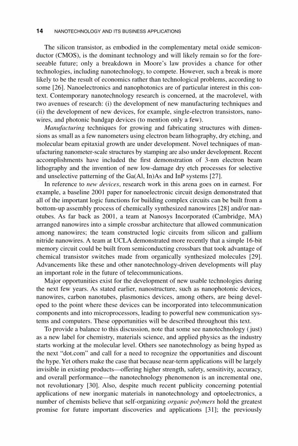
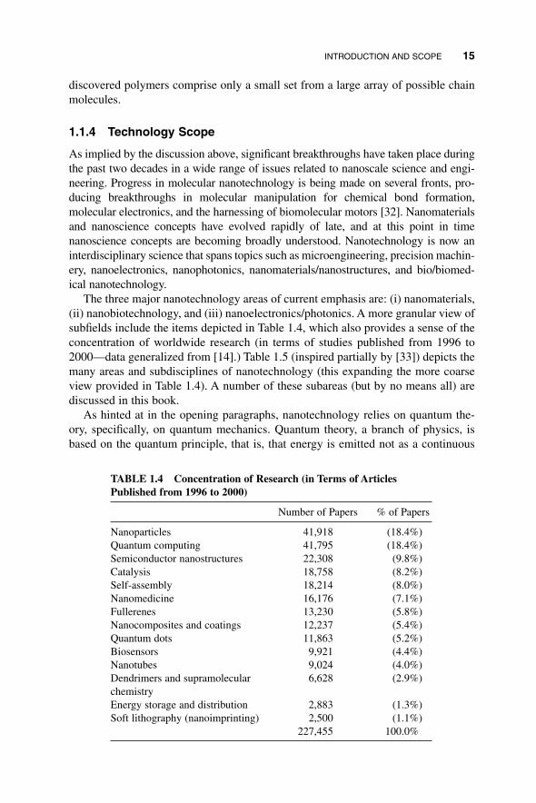
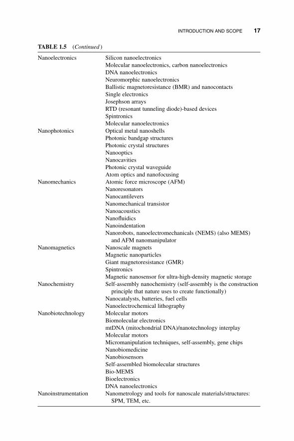
The three major nanotechnology areas of current emphasis are: (i) nanomaterials,(ii) nanobiotechnology, and (iii) nanoelectronics/photonics. A more granular view ofsubfields include the items depicted in Table 1.4, which also provides a sense of theconcentration of worldwide research (in terms of studies published from 1996 to2000—data generalized from [14].) Table 1.5 (inspired partially by [33]) depicts themany areas and subdisciplines of nanotechnology (this expanding the more coarseview provided in Table 1.4). A number of these subareas (but by no means all) arediscussed in this book.
As hinted at in the opening paragraphs, nanotechnology relies on quantum the-ory, specifically, on quantum mechanics. Quantum theory, a branch of physics, isbased on the quantum principle, that is, that energy is emitted not as a continuous
INTRODUCTION AND SCOPE 15
TABLE 1.4 Concentration of Research (in Terms of ArticlesPublished from 1996 to 2000)
Number of Papers % of Papers
Nanoparticles 41,918 (18.4%)Quantum computing 41,795 (18.4%)Semiconductor nanostructures 22,308 (9.8%)Catalysis 18,758 (8.2%)Self-assembly 18,214 (8.0%)Nanomedicine 16,176 (7.1%)Fullerenes 13,230 (5.8%)Nanocomposites and coatings 12,237 (5.4%)Quantum dots 11,863 (5.2%)Biosensors 9,921 (4.4%)Nanotubes 9,024 (4.0%)Dendrimers and supramolecular 6,628 (2.9%)chemistryEnergy storage and distribution 2,883 (1.3%)Soft lithography (nanoimprinting) 2,500 (1.1%)
227,455 100.0%
Minoli_ch01.qxd 9/27/2005 8:49 AM Page 15
16 NANOTECHNOLOGY AND ITS BUSINESS APPLICATIONS
TABLE 1.5 Taxonomy of Areas and Subdisciplines in the Nanotechnology Field
Nanostructured Nanofunctional materialsmaterials Nanoparticles
Carbon nanotubesCarbon nanotube “peapod”NanodiamondNanowiresNanorodsNanostructured polymerNanoscale manipulation of polymersNanostructured coatingsNanocatalysisNanocrystalsNanocrystals in Si-based semiconductorsNanocrystalline materials and nanocompositesThin-film photonic crystalsBiomolecules
Nanomaterials Nanoparticlessynthesis and Carbon nanotubeassembly Nanomachining
NanodepositionSol–gel methodsBall-millingNanocomposites
Nanofabrication “Top-down” approaches: lithography (E-beam, extreme methods ultraviolet); Dip-Pen nanolithography
“Bottom-up” approaches: selective growth; self-assembly; scanning tip manipulation
Nanomanipulation Scanning probe microscope-based nanomanipulatorNanotweezer
Nanolithography Scanning probe microscope (SPM)Dip-pen nanolithographyExtreme ultraviolet (EUV)Electron beam nanolithography/X-rayFocused ion beamLight coupling nanolithographyImprint nanolithography
Nanosensors Nanotube and nanowire sensorsNanocomposite sensor
Quantum behaviors Moore’s law/scaling and limits of CMOSand scaling limit Quantum theory/mechanicsof CMOS Wave interference, quantum mechanics, tunneling,
diffractionQuantum dotsQuantum wiresQuantum wellsQuantum corrals
Minoli_ch01.qxd 9/27/2005 8:49 AM Page 16
INTRODUCTION AND SCOPE 17
TABLE 1.5 (Continued )
Nanoelectronics Silicon nanoelectronicsMolecular nanoelectronics, carbon nanoelectronicsDNA nanoelectronicsNeuromorphic nanoelectronicsBallistic magnetoresistance (BMR) and nanocontactsSingle electronicsJosephson arraysRTD (resonant tunneling diode)-based devicesSpintronicsMolecular nanoelectronics
Nanophotonics Optical metal nanoshellsPhotonic bandgap structuresPhotonic crystal structuresNanoopticsNanocavitiesPhotonic crystal waveguideAtom optics and nanofocusing
Nanomechanics Atomic force microscope (AFM)NanoresonatorsNanocantileversNanomechanical transistorNanoacousticsNanofluidicsNanoindentationNanorobots, nanoelectromechanicals (NEMS) (also MEMS)
and AFM nanomanipulatorNanomagnetics Nanoscale magnets
Magnetic nanoparticlesGiant magnetoresistance (GMR)SpintronicsMagnetic nanosensor for ultra-high-density magnetic storage
Nanochemistry Self-assembly nanochemistry (self-assembly is the construction principle that nature uses to create functionally)
Nanocatalysts, batteries, fuel cellsNanoelectrochemical lithography
Nanobiotechnology Molecular motorsBiomolecular electronicsmtDNA (mitochondrial DNA)/nanotechnology interplayMolecular motorsMicromanipulation techniques, self-assembly, gene chipsNanobiomedicineNanobiosensorsSelf-assembled biomolecular structuresBio-MEMSBioelectronicsDNA nanoelectronics
Nanoinstrumentation Nanometrology and tools for nanoscale materials/structures:SPM, TEM, etc.
Minoli_ch01.qxd 9/27/2005 8:49 AM Page 17
quantity but in discrete discontinuous units. Quantum theory is the science of allcomplex elements of atomic and molecular spectra and the interaction of radiationand matter [34]. Quantum physics/mechanics principles will be covered in this text.Table 1.6 identifies some key terms of interest in nanotechnology; other terms areprovided in the Glossary at the end of the book. Related to the Glossary, we havemade every effort to include as many of the terms used in this text as possible.Hence, unfamiliar terms should, in most instances, be defined in the glossary.
1.1.5 Commercialization Scope
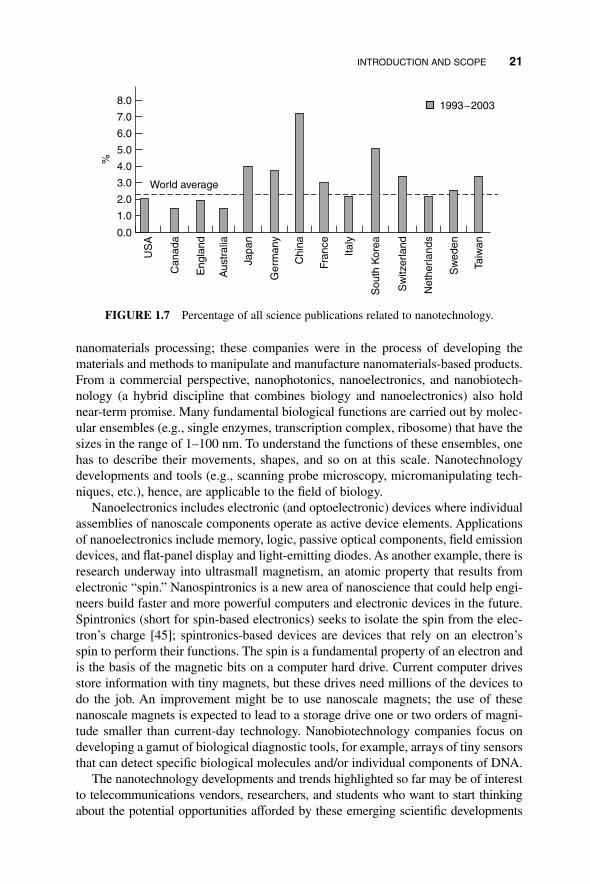
Commercial R&D work is now being focused on nanotechnology in order to translatethe pure science discoveries into usable products. While there is extensive academicand institutional interest and activity, there is also rapidly expanding commercial activ-ity. Significant nanotechnology research work has been undertaken in recent years atthe six national Nanoscale Science and Engineering Centers, located at ColumbiaUniversity (New York), Cornell University (Ithaca, NY), Rensselaer PolytechnicInstitute (Troy, NY), Harvard University (Cambridge, MA), Northwestern University(Evanston, IL), and, Rice University (Houston). In the past few years there has been alot of coverage on nanotechnology in scientific journals, at conferences, in universityprograms, in market research reports, and even in the financial and business press (inthe United States, press-time network TV advertisements from NEC also extolled thevirtues of nanotechnology). For example, in 2002 Merrill Lynch published the firstnanotechnology equity report. Science Magazine named nanotechnology the 2001Breakthrough of the Year,10 and quantum dot nanocrystals (“tiny” 5- to 10-nm semi-conductor nanocrystals that glow in various colors when excited by laser light and usedto tag biological molecules) were named by Science Magazine as Breakthrough of theYear #5 in 2003 [35]. High-tech companies such as, but not limited to, NEC have high-lighted its nanotechnology research in its corporate ads. There are now hundreds oflabs, companies, and academic institutions involved in this work (ranging at the cor-porate level, to name a few, from IBM, Intel, NEC, and HP to Veeco Instruments,Perkin-Elmer, and FEI Corp). As of the early 2000s there were more than 100 startupsdeveloping nanotechnology-based products that will be marketable in the 2005–2007timeframe. Figure 1.7 (based on data from [14]) shows that some countries are focus-ing more research (as a percentage of the total scientific publications) on nanotechnol-ogy than other countries. This book is a step in the direction of advocating practicalattention to this field, specifically from a computing and telecom perspective.
As noted in the previous section, at a macrolevel, commercially focused researchfalls into six functional categories, as follows: (i) nanomaterials and nanomateri-als processing, (ii) nanophotonics, (iii) nanoelectronics, (iv) nanoinstrumentation,(v) nanobiotechnology, and (vi) software. This is generally how this book is organ-ized (with the exception of nanobiotechnology, which is not covered here.) As a pointof reference, in 2002 there were around 50 companies focused on nanomaterials and
18 NANOTECHNOLOGY AND ITS BUSINESS APPLICATIONS
10Science Magazine cited work of the team at Nanosys Incorporated (Cambridge, MA) that arrangednanowires into a simple crossbar architecture that allowed communication among nanowires.
Minoli_ch01.qxd 9/27/2005 8:49 AM Page 18
INTRODUCTION AND SCOPE 19
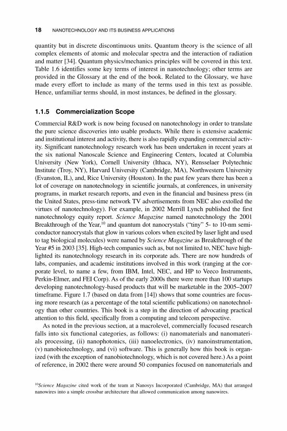
TABLE 1.6 Glossary of Key Nanotechnology-Related Terms Assembled from Various Scientific Sources
Buckminsterfullerene Most famous of the fullerenes, it is a nanostructure composed of (aka Buckyball, C60) 60 atoms of carbon arranged in a perfectly symmetric closed
cage. Discovered in 1985 by Richard Smalley, Harold Kroto,and Robert Curl for which they won the 1996 Nobel Prize in chemistry [36].
Carbon nanotube Cylinder-shaped structure resembling a rolled-up sheet of graphite (carbon) that can be a conductor or semiconductor depending on the alignment of its carbon atoms. It is 100 times stronger than steel of the same weight, although due to high fabrication costs, widespread commercial use is still distant [36].
Fullerene Third form of carbon, after diamond and graphite. Can be spherical or tubular in shape [36].
Nanotechnology Creation and utilization of materials, devices, and systems through the control of matter on the nanometer-length scale,that is, at the level of atoms, molecules, and supramolecular structures [37].
Quanta a. Fundamental units of energy.b. Light can carry energy only in specific amounts, proportional
to the frequency, as though it came in packets. The term quanta was given to these discrete packets of electromagnetic energy by Max Planck [38].
c. Smallest physical units into which something can be partitioned,according to the laws of quantum mechanics. For example,photons are the quanta of the electromagnetic field [38].
d. Each particle is surrounded by a field for each of the kinds of charges it carries, such as an electromagnetic field if it has electric charge. In the quantum theory, the field is described as made up of particles that are the quanta of the field. More loosely, the smallest amount of something that can exist [38].
Quantum chemistry Application of quantum mechanics to the study of chemical phenomena.
Quantum device Semiconductor device whose operation is based on quantum effects [36, 39].
Quantum dot (QD) Nanometer-scale “boxes” for selectively holding or releasing electrons; the size of the box can be from 30 to 1000 nm [40, 41]. Something (usually a semiconductor island) capable of confining a single (or a few) electron and in which the electrons occupy discrete energy states just as they would in an atom [42]. QDs are grouping of atoms so small that the addition or removal of an electron will change its properties in a significant way [36]. QDs are small devices fabricated in semiconductor materials that contain a tiny droplet of free electrons; the size and shape of these structures and, hence, the number of electrons theycontain, can be precisely controlled; a QD can have from a single electron to a collection of several thousands [43, 44].
Minoli_ch01.qxd 9/27/2005 8:49 AM Page 19
20 NANOTECHNOLOGY AND ITS BUSINESS APPLICATIONS
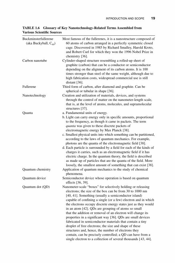
TABLE 1.6 (Continued)
Quantum effect Properties of transistors and wires become altered at the nanoscale level, so that they can no longer be characterized by classical electronic circuit theory. Quantum effects, such as the quantization of electronic charge and the interfering wave properties of electrons as they propagate through transistors and wires, need to be take into account [36].
Quantum electronics Name used for those parts of quantum optics that have practical device applications [36, 38].
Quantum optics Science concerned with the applications of the quantum theory of optics; i.e., optics defined in terms of the quanta of radiant energy or photons [34].
Quantum physics Physics based upon the quantum principle that energy is emitted not as a continuum but in discrete units [38].
Quantum theory a. General term describing quantum physics.b. Theory that seeks to explain that the action of forces is a
result of the exchange of subatomic particles [38].c. Theory used to describe physical systems that are very small, of
atomic dimensions or less. A feature of the theory is that certain quantities (e.g., energy, angular momentum, light) can only exist in certain discrete amounts, called quanta.
d. Initially, the theory developed by Planck that radiating bodies emit energy not in a continuous stream but in discrete units called quanta, the energy of which is directly proportional to the frequency. Now, all aspects of quantum mechanics.
e. Quantum theory provides the rules with which to calculate howmatter behaves. Once scientists specify what system they want to describe and what the interactions among the parti-cles of the system are, then the equations of the quantum theory are solved to learn the properties of the system.
Quantum well (QW) In a diode laser, a region between layers of gallium arsenide and aluminum gallium arsenide, where the density of electrons is very high, resulting in increased lasing efficiency and reduced generation of heat [34]. Semiconductor heterostructure fabricated to implement quantum effects in electronic and photonic applications; typically an ultrathin layer of narrower bandgap semiconductor is sandwiched between two layers of larger bandgap semiconductor; electrons and holes are free to move in the direction perpendicular to the crystal growth direction but not in the direction of crystal growth, hence,they are “confined” [36, 39].
Quantum wire Narrow channel created by cleaving a crystal made of alternating layers of gallium arsenide and aluminum gallium arsenide, and adding additional layers on the cleaved end face, at right angles to the first, resulting in an efficient diode laser [34].
Minoli_ch01.qxd 9/27/2005 8:49 AM Page 20
nanomaterials processing; these companies were in the process of developing thematerials and methods to manipulate and manufacture nanomaterials-based products.From a commercial perspective, nanophotonics, nanoelectronics, and nanobiotech-nology (a hybrid discipline that combines biology and nanoelectronics) also holdnear-term promise. Many fundamental biological functions are carried out by molec-ular ensembles (e.g., single enzymes, transcription complex, ribosome) that have thesizes in the range of 1–100 nm. To understand the functions of these ensembles, onehas to describe their movements, shapes, and so on at this scale. Nanotechnologydevelopments and tools (e.g., scanning probe microscopy, micromanipulating tech-niques, etc.), hence, are applicable to the field of biology.
Nanoelectronics includes electronic (and optoelectronic) devices where individualassemblies of nanoscale components operate as active device elements. Applicationsof nanoelectronics include memory, logic, passive optical components, field emissiondevices, and flat-panel display and light-emitting diodes. As another example, there isresearch underway into ultrasmall magnetism, an atomic property that results fromelectronic “spin.” Nanospintronics is a new area of nanoscience that could help engi-neers build faster and more powerful computers and electronic devices in the future.Spintronics (short for spin-based electronics) seeks to isolate the spin from the elec-tron’s charge [45]; spintronics-based devices are devices that rely on an electron’sspin to perform their functions. The spin is a fundamental property of an electron andis the basis of the magnetic bits on a computer hard drive. Current computer drivesstore information with tiny magnets, but these drives need millions of the devices todo the job. An improvement might be to use nanoscale magnets; the use of thesenanoscale magnets is expected to lead to a storage drive one or two orders of magni-tude smaller than current-day technology. Nanobiotechnology companies focus ondeveloping a gamut of biological diagnostic tools, for example, arrays of tiny sensorsthat can detect specific biological molecules and/or individual components of DNA.
The nanotechnology developments and trends highlighted so far may be of interestto telecommunications vendors, researchers, and students who want to start thinkingabout the potential opportunities afforded by these emerging scientific developments
INTRODUCTION AND SCOPE 21
8.0
7.0
6.0
5.0
4.0
3.0
2.0
1.0
0.0
US
A
%
Can
ada
Eng
land
Aus
tral
ia
Japa
n
Ger
man
y
Chi
na
Fran
ce
Italy
Sou
th K
orea
Sw
itzer
land
Net
herla
nds
Sw
eden
Taiw
an
World average
1993−2003
FIGURE 1.7 Percentage of all science publications related to nanotechnology.
Minoli_ch01.qxd 9/27/2005 8:49 AM Page 21
and approaches for the next-generation networks to be deployed 5–10 years in thefuture; advanced planning is a valuable and effective exercise. For example, nanopho-tonics companies are developing highly integrated optical-communications compo-nents using nanooptic and nanomanufacturing technologies (nanomanufacturing asapplied to optical components allows rapid prototyping, performance improvements,smaller forms, and lower costs [12].) MEMSs are microscale systems (∼100 µm)(but not nanoscale yet) that include both mechanical and electrical devices integratedon a single die or chip. MOEMS consist of MEMS devices with integral opticalcomponents such as mirrors, lenses, filters, laser diodes, emitters or other optics. AMEMS system may include microfluidic elements, integral microelectronics or ICs,“lab-on-chip” systems, actuators, micromotors, or sensors. Lab-on-chip (also knownas nanolab) is a chip that uses (i) microfluidics to transport individual cells across thedevice, (ii) nanowire sensors ∼10 nm in diameter to identify genes and proteins in thecell, and, (iii) nanomechanical sensors to detect protein and gene interactions.
These and other nanoscale advances will be critical to the computing and telecomindustry in the coming decade; hence, the focus of this book.
1.1.6 Opportunities of the Technology and the 21st CenturyNanotechnology Research and Development Act of 2003
National Science Foundation (NSF11) representatives have been quoted as saying:“Some call [nanotechnology] the next industrial revolution, anticipating an eco-nomic bonanza that dollar for dollar, and job for job, will outstrip the introductionof electricity, the automobile or the new information and communications technolo-gies. . . . The expectations raised by nanotechnology have inspired governments world-wide to increase support for nanotechnology research and education, and sparkedinternational competition to bring nanotechnology from the bench to the boardroom”[46]. The NSF has recently being advocating for closer cooperation between thescientific and engineering research communities on nanotechnology development;this cooperation would create what has been dubbed “nanotransformations” in scientificand social fields.
From a current market point of view, there was an expectation that about $1 bil-lion would be invested in nanotech by the venture capital (VC) community in 2003(about 2% of the total VC pool of money), and most of that investment will bein software (e.g., computer-based development/modeling tools). Nanomaterials areestimated to have a $150 million market in the short term [47]. In addition to this pri-vate investment, there is government-based funding.
In late 2003, President George W. Bush signed the 21st Century NanotechnologyResearch and Development Act into law. The $3.7 billion appropriation, which earlierhad been approved by Congress, was to be divided among eight government agencies.Nanotechnology “has the potential to be the making of a revolution because it can bean enabling technology, fundamentally changing the way many items are designed andmanufactured,” said Rep. Mike Honda, D-Calif. “And we’ve all probably heard the
22 NANOTECHNOLOGY AND ITS BUSINESS APPLICATIONS
11The NSF invests over $3.3 billion per year in about 20,000 research and education projects in scienceand engineering.
Minoli_ch01.qxd 9/27/2005 8:49 AM Page 22
National Science Foundation prediction that the worldwide market for nanotechnologyproducts and services could reach $1 trillion by 2015.” The bill authorizes the presi-dent to create a permanent National Nanotechnology Research Program (NNRP) toreplace the expiring National Nanotechnology Initiative. The NNRP, according to thebill, is a “coordinated interagency program that will support long-term nanoscaleresearch and development leading to potential breakthroughs in areas such as materi-als and manufacturing, nanoelectronics, medicine and health care, environment, energy,chemicals, biotechnology, agriculture, information technology, and national and home-land security.” The act encourages the development of networked facilities linking aca-demic institutions, national labs and industry12 [48].
The act identifies a list of “grand challenges” as the long-term guiding principlesfor individual research groups and for the national Nanoscale Science and EngineeringCenters. Those grand challenges include [48]13: (i) To design materials (nanoelec-tronics, optoelectronics, and magnetics) that are stronger, lighter, harder, safer, andself-repairing. Health care applications are specifically cited and so are nanoscaleprocesses, environmental solutions, energy management, and energy conservation.(ii) To foster the development of economical, efficient, and safe transportation, includ-ing the development of microspacecraft that can overcome Earth’s gravity field whenblasting off and survive the rigors of space flight in a manner that is cheaper andmore environmentally friendly than current technology. (iii) To foster the develop-ment of biologically oriented nanodevices for detection and mitigation of biologi-cally based threats to humans.
These funding initiatives will be a major impetus to the science, the engineering,and the applications of nanotechnology. Hence, this practical book comes at anopportune time. We focus on applied technology and product development.
1.2 PRESENT COURSE OF INVESTIGATION
We have so far implied that at the nanoscale ordinary matter often displays surprisingproperties that can be exploited to increase computer speed and memory capacity andto manufacture materials that are stronger, lighter, and “smarter” by orders of mag-nitude. The underlying principles for nanoscale devices are significantly differentthan ordinary semiconductor techniques because the systems are so small that quan-tum effects govern their behavior. Recent developments in surface microscopy, silicon
PRESENT COURSE OF INVESTIGATION 23
12The president’s 2005 budget provides about $1 billion for the multiagency National NanotechnologyInitiative (NNI), a doubling over levels in 2001, the first year of the initiative. The 2005 budget request isdesigned to support the NNI activities of 10 federal agencies in order to advance understanding ofnanoscale phenomena [2].13The act also directs the establishment of a National Nanotechnology Coordination Office to handle day-to-day technical and administrative support and act as the point of contact on all federal nanotechnologyactivities for government organizations, academia, industry, professional societies, state nanotechnologyprograms, and others wishing to exchange technical and programmatic information. The act also seeks to“establish a new center for societal, ethical, educational, legal and work force issues related to nanotech-nology. . . to encourage, conduct, coordinate, commission, collect and disseminate research.” The act alsoauthorizes public hearings and expert advisory panels, as well as an American Nanotechnology PreparednessCenter that will study nanotechnology’s potential societal and ethical impact [48].
Minoli_ch01.qxd 9/27/2005 8:49 AM Page 23
fabrication, physical chemistry, and computational engineering have come togetherto help scientists better understand, fabricate, and manipulate structures at this level.The ability to construct matter and molecules one atom at a time, coupled with newmethods to fabricate novel materials and devices, has made the field of nanosciencean interesting discipline for both scientists and engineers [22].
Furthermore, nanotechnology operates at the dimension where the living and non-living worlds meet [46]. Quantum dots (grouping of atoms so small that the additionor removal of an electron alters the properties of the grouping in a significant way),nanowires, and related nanoscale structures are now key topics in contemporary semi-conductor research; this research is aimed at downsizing chip components to themolecular scale. These just-named factors and the issues listed earlier in the chaptermake this body of research a very interesting topic of investigation. As noted, in thistext we focus on telecom and networking applications of nanotechnology.
In the chapters that follow, we discuss at a high level the basic science (physics andchemistry) behind nanotechnology. In Chapters 2 (physics) and 3 (chemistry) we covertopics such as: physics and chemistry basics (e.g., electron, atoms, atomic structures,molecules, bonded structures), electrical properties (e.g., insulators, semiconductors,conductors), and chemical bonds and reactions. Chapter 2 also provides a basic intro-duction to transistors, in support of the discussion to follow in Chapter 6. It turns outthat while classical Newtonian mechanics can predict with precision the motions ofmasses ranging in size from microscopic particles to very large stars, it cannot predictthe behavior of the particles in the atomic domain; quantum theory comes into playinstead. Hence, taking off from the coverage of Chapters 2 and 3, in Appendices D andE we discuss some of the basic scientific principles that support this field; the readerwho may find these two appendices somewhat demanding may chose to skip this mate-rial and move on to the chapters that follow; which are generally self-contained.
In Chapter 4 we look at nanomaterials and nanomaterial processing: Individ-ual nanoparticles and nanostructure (e.g., nanotubes, nanowires) are discussed.Nanophotonics is discussed in Chapter 5 (e.g., nanocrystals, nanocrystal fibers).Nanoelectronics (e.g., metal nanoclusters, semiconducting nanoclusters, nanocrystals,quantum dots) is covered in Chapter 6. Both Chapters 5 and 6 provide a discussion ofnear-term and longer-term applications to the field of computers, telecommunications,and networking. Appendix F discusses nanoinstrumentation, while Appendices A, B,and C provide other background material. Appendix G provides information onquantum computing.
The goal of this book is to provide a self-contained, reasonably pedagogical intro-duction to the field for professionals wanting to obtain an entry-level view of thisrapidly evolving field. It is not the purpose of this book to be a research monogramfor the in-field scientist, nor to describe ultrarecent research breakthroughs. Thetreatment is not intended to be exhaustive: We only survey some of the more well-established/well-developed areas. We believe that we have provided for the prospec-tive reader a reasonable mix of technical (introductory) material and a sense of theapplications to enable the practitioner to get started in this field.
24 NANOTECHNOLOGY AND ITS BUSINESS APPLICATIONS
Minoli_ch01.qxd 9/27/2005 8:49 AM Page 24