modeling and design of high-resolution sigma-delta
TRANSCRIPT
MODELING AND DESIGN OF
HIGH-RESOLUTION
SIGMA-DELTA MODULATORS
A DISSERTATION
SUBMITTED TO THE DEPARTMENT OF
ELECTRICAL ENGINEERING
AND THE COMMITTEE ON GRADUATE STUDIES
OF STANFORD UNIVERSITY
IN PARTIAL FULFILLMENT OF THE REQUIREMENTS
FOR THE DEGREE OF
DOCTOR OF PHILOSOPHY
IN
ELECTRICAL ENGINEERING
Louis Albert Williams III
August 1993

ii
© Copyright by Louis Albert Williams III 1993
All Rights Reserved

iii
I certify that I have read this dissertation and that in my opinion it is fully adequate,
in scope and quality, as a dissertation for the degree of Doctor of Philosophy.
Bruce A. Wooley (Principal Advisor)
I certify that I have read this dissertation and that in my opinion it is fully adequate,
in scope and quality, as a dissertation for the degree of Doctor of Philosophy.
Robert W. Dutton
I certify that I have read this dissertation and that in my opinion it is fully adequate,
in scope and quality, as a dissertation for the degree of Doctor of Philosophy.
Robert M. Gray
Approved for the University Committee on Graduate Studies:

iv
Abstract
Analog-to-digital (A/D) conversion based on sigma-delta modulation has enjoyed
increasing popularity in a wide variety of applications. Through the use of oversampling,
noise shaping, and coarse quantization, sigma-delta modulation provides a means of
achieving high-resolution A/D conversion without requiring precise component matching.
In this dissertation, a method for analytically modeling sigma-delta modulators is pro-
posed, and an implementation of an audio-band converter design based on the results of
this modeling is described.
Analytical modeling of oversampling A/D converters is complicated by the presence
of a strong non-linearity in the modulator’s feedback loop. In this research a combination
of describing functions, approximations, and empirical fits have been used to develop a
method for modeling this nonlinearity. The model, referred to herein as the adaptive gain
model, can be used to evaluate concisely the influence of various parameters on the per-
formance of a modulator and choose values that represent the best design compromise
between the quantization noise at low-level inputs and the overload characteristics at high-
level inputs.
Circuit design for high-resolution A/D converters based on sigma-delta modulation
involves simultaneously achieving low noise performance while accommodating large
input signal levels. Modulator parameters derived from the adaptive gain model and reso-
lution enhancing techniques in the architecture and the integrator circuits within that
architecture have been used to design an experimental audio-band converter. Based on a
third-order cascaded architecture comprising a second-order modulator followed by a
first-order modulator and implemented in a 1-µm CMOS process, the experimental con-
verter achieves a dynamic range of 104 dB at a signal bandwidth of 25 kHz while operat-
ing from a single 5-V supply.
v
Acknowledgments
The completion of this dissertation would not have been possible without the support
and encouragement of many people, including colleagues, advisors, friends, and associ-
ates. First and foremost, I wish to thank Professor Bruce Wooley for his support and guid-
ance. By allowing freedom in the course of my research while requiring significant and
useful results, he enabled me to go beyond the original scope of my research and explore
areas such as the adaptive gain model described in Chapter 3. I also appreciate and have
benefited greatly from his emphasis on producing high quality publications. Among the
other faculty at Stanford, I am indebted to Professors Robert Dutton and Robert Gray for
the review of this dissertation, and to Professor Teresa Meng for serving on my oral exam-
ination committee. As I recall, it was Professor Dutton who indirectly introduced me to
Professor Wooley some five years ago.
Among my colleagues, Dr. Brian Brandt deserves special recognition. While a student
here at Stanford, his assistance was instrumental in the initial phases of my research.
Later, as a member of the Semiconductor Process and Design Center at Texas Instruments
Incorporated, his support was invaluable. I am grateful to him and the other members of
that research group for the fabrication of the experimental circuit described in this disser-
tation.
Many other students have contributed significantly to my research. I would like to
thank Dr. Behzad Razavi and Dr. Peter Lim for their circuit expertise, Marc Loinaz and
Dave Su for helping to develop our current test methodology, Drew Wingard for being the
resident unpaid Magic expert, and Tallis Blalack for his bond pad experiments.
Among the staff, I am most grateful to Ann Guerra for her amazing ability to cut
through the Stanford bureaucracy and for being the most organized person on the face of
the earth. Irene Sweeney, having the misfortune of being in the office adjacent to mine,
has always been willing to answer my questions. Charley Orgish and Laura Schrager also
need to be commended for their support of the computer systems.

vi
Most of all, I am grateful for the love, support, and patience of my family. The caring
and encouragement of my parents, Louis and Patricia Williams, my wife Beverly, and my
daughter Rachel, have greatly enriched my life. I am especially indebted to Bev for sur-
viving her tenure as the wife of a starving student.
This dissertation is dedicated to my grandfathers Louis Williams Sr. and Howard
Plummer.

vii
Table of Contents
Abstract .............................................................................................................................. iv
Acknowledgments ...............................................................................................................v
List of Tables .......................................................................................................................x
List of Figures .................................................................................................................... xi
1 Introduction 1
1.1 Organization..........................................................................................................2
1.2 Simulation Details.................................................................................................3
2 Analog-to-Digital Conversion 4
2.1 Nyquist-Rate Converters.......................................................................................4
2.1.1 Limitations of Nyquist-Rate Converters...................................................8
2.2 Oversampled A/D Converters...............................................................................8
2.3 Feedback A/D Converters...................................................................................10
2.4 Noise-Differencing Sigma-Delta Modulators.....................................................12
2.4.1 Considerations in High-Performance Audio...........................................15
2.5 Cascaded Sigma-Delta Modulators ....................................................................17
2.5.1 1-1-1 Architecture...................................................................................18
2.5.2 2-1 Architecture ......................................................................................22
2.6 Spectral Tones.....................................................................................................24
2.7 Summary.............................................................................................................33
3 Adaptive Gain Model 34
3.1 Describing Function Representation...................................................................35
3.2 The White Noise Approximation........................................................................38
3.2.1 Quantizer Error Power Spectrum............................................................38
3.2.2 The Quasi-Static Approximation ............................................................40
3.2.3 Linear System Analysis ..........................................................................43
viii
3.3 Quantizer Error Variance....................................................................................43
3.3.1 Statistical Properties of the Error Variance ............................................44
3.3.2 The Spread Factor ...................................................................................45
3.3.3 Error Variance Estimation ......................................................................46
3.4 Modeling the 2-1 Architecture............................................................................48
3.4.1 Baseband .................................................................................................50
3.4.2 First Stage ...............................................................................................51
3.4.3 Second Stage...........................................................................................53
3.4.4 Results.....................................................................................................55
3.5 Summary.............................................................................................................59
4 Modulator Design 60
4.1 Modulator Building Blocks ................................................................................60
4.2 Circuit Noise .......................................................................................................63
4.2.1 Noise Reduction......................................................................................64
4.2.2 Noise Shaping in the Modulator .............................................................66
4.2.3 Noise Sources .........................................................................................67
4.2.4 Switch Noise ...........................................................................................68
4.3 Integrator Circuits ...............................................................................................70
4.3.1 Continuous-Time Integrators ..................................................................70
4.3.2 Sampled-Data Integrator.........................................................................72
4.3.3 Correlated Double Sampling Integrator..................................................74
4.4 Amplifier Design ................................................................................................75
4.4.1 Single-Stage Amplifier ...........................................................................76
4.4.2 Two-Stage Amplifier ..............................................................................78
4.5 Integrator Limitations .........................................................................................80
4.5.1 Integrator Speed ......................................................................................80
4.5.2 Integrator Leak........................................................................................82
4.5.3 Signal Swing ...........................................................................................84
4.6 Specifications for the 2-1 Modulator ..................................................................86
4.6.1 Integrator Gains ......................................................................................86
4.6.2 Circuit Specifications..............................................................................87
4.7 Summary.............................................................................................................89
5 Implementation 90
5.1 The Integrators ....................................................................................................92
ix
5.1.1 The First Integrator .................................................................................93
5.1.2 The First Amplifier .................................................................................96
5.1.3 The Second and Third Integrators ........................................................100
5.2 Other Circuitry ..................................................................................................106
5.2.1 Comparator-D/A Subsystem.................................................................106
5.2.2 Clock Generators ..................................................................................111
5.3 Experimental Results ........................................................................................115
5.4 Summary...........................................................................................................121
6 Test Setup 122
7 Conclusion 130
7.1 Recommendations for Further Investigation ....................................................131
References 133

x
List of Tables
2.1 Required oversampling ratios. ...............................................................................15
4.1 Integrator gain values.............................................................................................87
5.1 Switch types and sizes. ..........................................................................................96
5.2 Second integrator switches. .................................................................................103
5.3 Third integrator switches. ....................................................................................103
5.4 Modulator performance. ......................................................................................117
6.1 Test setup equipment list. ....................................................................................124
xi
List of Figures
2.1 Nyquist-rate A/D converter. ....................................................................................5
2.2 Uniform quantizer transfer function. .......................................................................5
2.3 Quantizer error. ........................................................................................................6
2.4 Quantizer error distribution. ....................................................................................6
2.5 Oversampled A/D converter. ...................................................................................9
2.6 Feedback modulator...............................................................................................10
2.7 Integrating sigma-delta modulator.........................................................................12
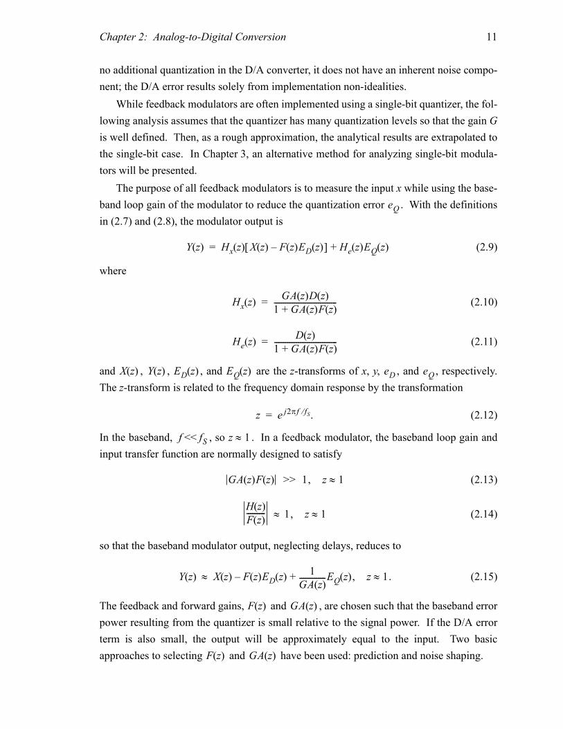
2.8 Calculated dynamic range vs. oversampling ratio. ................................................14
2.9 Cascaded modulator architecture. ..........................................................................17
2.10 1-1-1 Architecture..................................................................................................18
2.11 Effect of matching errors in the 1-1-1 architecture................................................21
2.12 2-1 Architecture. ....................................................................................................22
2.13 Effect of matching errors in the 2-1 architecture. ..................................................25
2.14 (a) Output sequence with average of 0.0005. (b) Running average of (a)............26
2.15 Spectral tone in a second-order modulator. ...........................................................27
2.16 Spectral tones in a fourth-order modulator. ...........................................................27
2.17 Tone power vs. dc input level for a second-order modulator, b = 2.0. ..................28
2.18 Tone power vs. dc input level for a second-order modulator, b = 2.5. ..................29
2.19 Colored spectrum of a second-order modulator with b = 2.5. ...............................30
2.20 Tone power vs. dc input level for a fourth-order modulator. ................................30
2.21 Tone elimination in the 2-1 architecture................................................................31
2.22 Tone power vs. dc input level for the 2-1 architecture. .........................................32
3.1 Generalized sigma-delta modulator. ......................................................................36
3.2 Describing function superposition of random and bias systems............................37
3.3 Error power spectrum for pure dc input.................................................................39
3.4 Error power spectrum with input noise..................................................................40
3.5 Error power spectrum in a cascaded stage.............................................................41

xii
3.6 The peaking function. ............................................................................................47
3.7 2-1 Architecture. ....................................................................................................48
3.8 Quantizer error variance and gain vs. the input mean. ..........................................52
3.9 Variance-gain ratio vs. the input mean. .................................................................53
3.10 Adaptive gain model and simulation comparison..................................................56
3.11 Noise and overload level trade-off.........................................................................57
3.12 Dynamic range vs. error gain.................................................................................57
3.13 Dynamic range vs. feedback coefficient................................................................58
3.14 Dynamic range vs. error mixing. ...........................................................................59
4.1 Integrator block diagram........................................................................................61
4.2 2-1 architecture implementation. ...........................................................................62
4.3 Small signal MOS model with noise. ....................................................................68
4.4 Switched capacitor noise subcircuit.......................................................................69
4.5 Continuous-time integrator. ...................................................................................70
4.6 Sampled-data integrator. ........................................................................................73
4.7 Correlated double sampling integrator. .................................................................74
4.8 Single-stage folded-cascode amplifier...................................................................76
4.9 Two-stage amplifier. ..............................................................................................78
4.10 Integrator speed SNDR contours. ..........................................................................81
4.11 Maximum integrator swings in the 2-1 architecture. .............................................85
5.1 2-1 architecture implementation. ...........................................................................91
5.2 Clock phase timing diagram. .................................................................................92
5.3 The first integrator. ................................................................................................93
5.4 (a) Standard transmission gate. (b) Linear resistance transmission gate. .............94
5.5 Switch resistance vs. input voltage for standard transmission gates
and linear resistance transmission gates (WS = 10 µm). ..................................95
5.6 The amplifier for the first integrator. .....................................................................97
5.7 Common-mode feedback for the first amplifier. ...................................................98
5.8 First amplifier bias circuitry. .................................................................................99
5.9 The second integrator...........................................................................................101
5.10 The third integrator. .............................................................................................102
5.11 The amplifier for the second and third integrators. .............................................104
5.12 Common-mode feedback for the second and third amplifiers.............................104
5.13 Second and third amplifier bias circuitry.............................................................105
5.14 Comparator-D/A subsystem. ...............................................................................106
5.15 The differential comparator. ................................................................................108

xiii
5.16 The differential SR latch......................................................................................109
5.17 The feedback D/A converter. ...............................................................................110
5.18 Differential current-mode output buffer. .............................................................112
5.19 Non-overlapping clock generator. .......................................................................113
5.20 Differential NOR gate..........................................................................................114
5.21 Die photomicrograph of the 2-1 architecture implementation.............................116
5.22 Measured signal-to-noise+distortion ratio. ..........................................................117
5.23 Reduced SNDR degradation with a 6-V supply ..................................................118
5.24 Output spectrum for −10-dB 2-kHz input............................................................118
5.25 Measured dynamic range versus oversampling ratio...........................................119
5.26 Measured tone reduction in the 2-1 architecture. ................................................120
6.1 Experimental test setup. .......................................................................................123
6.2 Differential sinewave generator load circuit........................................................124
6.3 Voltage bias generator. ........................................................................................125
6.4 6 V voltage reference. ..........................................................................................126
6.5 Current generators................................................................................................126
6.6 7 V voltage reference. ..........................................................................................127
6.7 −2 V voltage reference.........................................................................................127
6.8 LC decoupling circuit. .........................................................................................127
6.9 RC decoupling circuit. .........................................................................................127

1
Chapter
1 Introduction
With the continued scaling of integrated circuit technologies and digital storage media,
digital signal processing systems have supplanted their analog counterparts in many appli-
cations. In audio systems, for example, this displacement has been evident both in the
consumer and communications markets. The compact disc has replaced the long-play
record to such a degree that many “record” stores no longer sell records, and the digital
audio tape may soon do the same to the cassette tape. Telecommunication networks are
digital internally, and, with the advent of ISDN, even the external consumer link is becom-
ing digital.
Since digitally processed signals usually originate in the analog domain and once pro-
cessed must be returned to the analog domain, the proliferation of digital processing sys-
tems has generated the need for high-performance analog-to-digital (A/D) and digital-to-
analog (D/A) converters. Many factors, including cost, reliability, and speed, have fueled
the desire to implement these converters in the same integrated circuit technologies that
provide the inexpensive, high-speed medium for digital processor design. However, the
precision with which components match in scaled integrated circuit technologies is often
less than the desired converter precision and thereby limits the accuracy that can be
achieved in A/D and D/A converters.
In applications such as digital audio, in which the signal bandwidth is much less than
the operating speeds typical in digital circuits, a technique called sigma-delta modulation
can be used to overcome limited device matching and achieve high resolution perfor-
mance. In a sigma-delta modulator, a combination of oversampling, negative feedback,
and filtering is used to trade speed for resolution. While this technique is applicable to
both A/D and D/A conversion in many signal processing applications, this research
focuses on the design and implementation of a high-resolution audio-band A/D converter
using sigma-delta modulation.
Chapter 1: Introduction 2
Previous research has demonstrated the feasibility of using sigma-delta modulation in
high-resolution audio applications [1, 2]. This work seeks to discover the factors that ulti-
mately limit the resolution, or dynamic range, of sigma-delta converters. The specific
goal is to demonstrate a sigma-delta modulator architecture capable of a dynamic range of
better than 100 dB for a signal bandwidth of 25 kHz when integrated in a digital-compati-
ble 5-V CMOS technology.
A complete sigma-delta A/D converter comprises two main components: a modulator
and a decimation filter. The modulator is an analog circuit and usually limits the perfor-
mance of the converter. The decimation filter is a digital circuit and usually occupies most
of the circuit area. Both offer challenging areas of research, but this work concentrates on
the performance limiting component — the modulator. All decimation filtering, both for
simulations and experimental measurements, is done by computer as described in
Section 1.2.
1.1 Organization
Following this introduction, several aspects of sigma-delta A/D conversion are covered in
detail. Chapter 2 begins with a description of the classic Nyquist-rate A/D converter and
uses this both as an introduction to the concepts involved in A/D conversion and as a basis
for evaluating the merits of other A/D conversion techniques. This analysis is expanded to
include oversampling converters and feedback modulators and then focuses on the class of
feedback modulators known as sigma-delta modulators. The theoretical performance of
various sigma-delta modulator architectures is compared using a simplifying approxima-
tion referred to herein as the unity gain approximation. Based on this comparison, an
architecture is chosen as the vehicle for achieving the design goals of this research.
In Chapter 3, a model of sigma-delta modulators is developed that is more detailed
than the unity gain approximation. Called the adaptive gain model, it uses the method of
describing functions to develop a partially analytic, partially empirical model accurate
enough to optimize the design parameters of a sigma-delta modulator architecture. This
model is used to select the gain coefficients for the architecture chosen in Chapter 2.
Turning from the theoretical to the practical, several design limitations at the architec-
tural level are discussed in Chapter 4. This discussion includes issues such as circuit out-
put signal range and thermal noise considerations. Techniques for overcoming these
limitations are described, and a circuit topology is outlined.
In Chapter 5, the actual circuit implementation of the high-resolution modulator devel-
oped in the preceding chapters is covered. Experimental results for a modulator prototype

Chapter 1: Introduction 3
fabricated in a 1-µm CMOS process are presented. This prototype exceeds the design
goal, achieving a dynamic of 104 dB for a signal bandwidth of 25 kHz. Issues specific to
testing a high-performance circuit such as this are covered in Chapter 6.
The results of the research are summarized in Chapter 7, and additional areas of
research are suggested.
1.2 Simulation Details
Throughout this work, the results of simulations of various modulator architectures are
used to verify analytic approximations and predict modulator performance. These simula-
tions were generated using the program MIDAS [3]. Spectra were estimated using a dis-
crete Fourier transform (DFT) in conjunction with a windowing function described by
Nuttall [4]. Autocorrelation and cross-correlation power spectra were estimated using a
variation on the technique described by Oppenheim and Schafer [5].
The decimation filtering was done using the MIDAS program. A two-step architec-
ture was used; the first stage was a comb filter [6] and the second stage was an FIR filter.
The FIR filter coefficients were generated using a program based on the Remez exchange
algorithm [7] that was modified to compensate for the droop of the comb filter [2].
4
Chapter
2 Analog-to-Digital
Conversion
Analog-to-digital (A/D) conversion is the process of transforming a continuous-time,
continuous-amplitude signal into a discrete-time, discrete-amplitude signal. It comprises
two fundamental operations: sampling and amplitude quantization. The performance of
an A/D converter is limited by its sampling speed and quantization accuracy; sampling
bounds the signal bandwidth and quantization produces noise. This chapter focuses on
quantization noise and the oversampling techniques that can be used to reduce its effect.
In the first section, basic quantization noise theory is reviewed through the description
of a Nyquist-rate A/D converter. Using this converter as a foundation, the discussion
expands to oversampling and feedback A/D converters and the quantization noise reduc-
tions they provide. The remainder of the chapter is devoted to one important class of feed-
back A/D converters, sigma-delta modulators. Both single-stage and cascaded sigma-
delta modulators are analyzed and compared. The chapter closes with a brief discussion
of the tones, or coloration, that can be present in the quantizer error spectrum of a sigma-
delta modulator.
2.1 Nyquist-Rate Converters
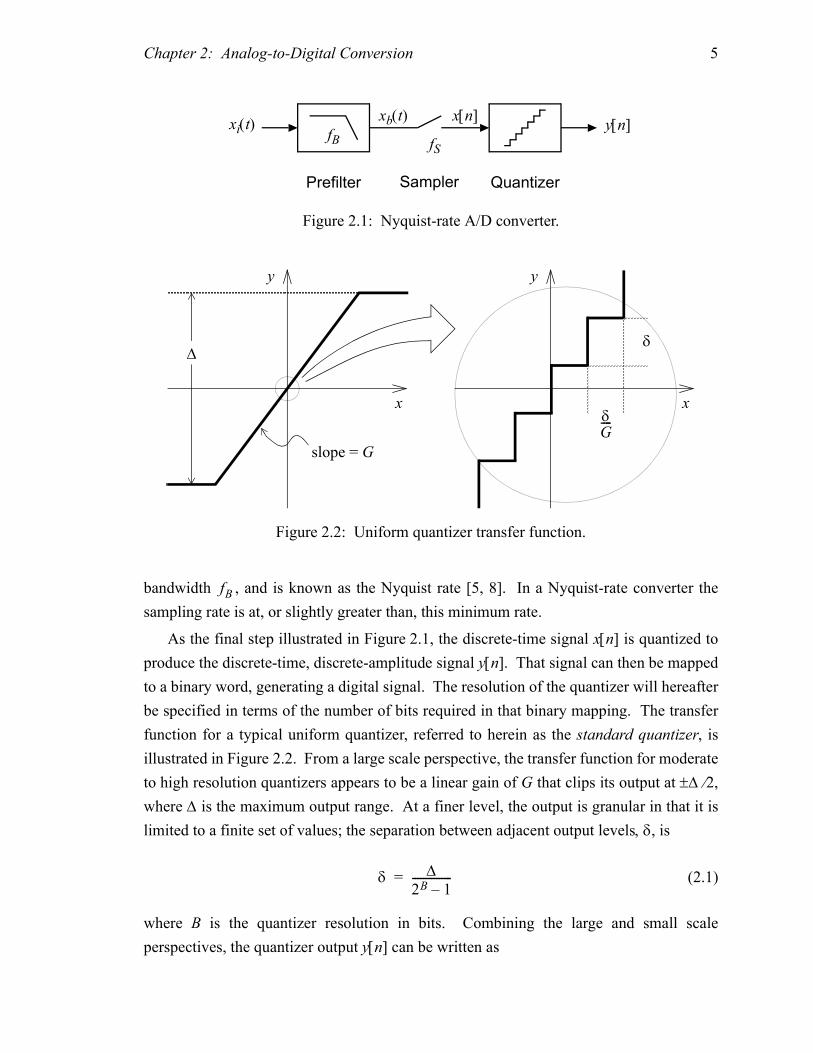
The block diagram of a structure that illustrates the basic functions in a Nyquist-rate con-
verter is shown in Figure 2.1. The input signal is lowpass filtered, restricting the
bandwidth of the resulting signal to . The bandlimited signal is sampled at
uniform time intervals with the sampling rate , producing the discrete-time signal x[n].
If the sampling rate is sufficiently high, there is no loss of information in the sampling pro-
cess. The minimum rate at which the signal can be sampled is twice the signal
xi t( )
xb t( ) fB xb t( )
fS
xb t( )
Chapter 2: Analog-to-Digital Conversion 5
bandwidth , and is known as the Nyquist rate [5, 8]. In a Nyquist-rate converter the
sampling rate is at, or slightly greater than, this minimum rate.
As the final step illustrated in Figure 2.1, the discrete-time signal x[n] is quantized to
produce the discrete-time, discrete-amplitude signal y[n]. That signal can then be mapped
to a binary word, generating a digital signal. The resolution of the quantizer will hereafter
be specified in terms of the number of bits required in that binary mapping. The transfer
function for a typical uniform quantizer, referred to herein as the standard quantizer, is
illustrated in Figure 2.2. From a large scale perspective, the transfer function for moderate
to high resolution quantizers appears to be a linear gain of G that clips its output at ±∆ ⁄ 2,
where ∆ is the maximum output range. At a finer level, the output is granular in that it is
limited to a finite set of values; the separation between adjacent output levels, δ, is
(2.1)
where B is the quantizer resolution in bits. Combining the large and small scale
perspectives, the quantizer output y[n] can be written as
fBxi(t)
xb(t) x[n]y[n]
Prefilter Sampler Quantizer
fS
Figure 2.1: Nyquist-rate A/D converter.
fB
Figure 2.2: Uniform quantizer transfer function.
x
y
∆
slope = G
δG----
δ
x
y
δ ∆2B 1–---------------=
Chapter 2: Analog-to-Digital Conversion 6
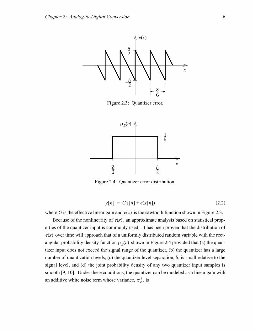
(2.2)
where G is the effective linear gain and is the sawtooth function shown in Figure 2.3.
Because of the nonlinearity of , an approximate analysis based on statistical prop-
erties of the quantizer input is commonly used. It has been proven that the distribution of
over time will approach that of a uniformly distributed random variable with the rect-
angular probability density function shown in Figure 2.4 provided that (a) the quan-
tizer input does not exceed the signal range of the quantizer, (b) the quantizer has a large
number of quantization levels, (c) the quantizer level separation, δ, is small relative to the
signal level, and (d) the joint probability density of any two quantizer input samples is
smooth [9, 10]. Under these conditions, the quantizer can be modeled as a linear gain with
an additive white noise term whose variance, , is
y[n] Gx[n] e x[n]( )+=
e x( )
δG----
δ2---–
δ2---
e x( )
x
Figure 2.3: Quantizer error.
e x( )
e x( )
ρE e( )
δ2---δ
2---–
1δ---
ρE e( )
e
Figure 2.4: Quantizer error distribution.
σe2

Chapter 2: Analog-to-Digital Conversion 7
(2.3)
This model, referred to hereafter as Bennett’s noise model, forms the basis of much of the
analysis in this work.
Unfortunately, many of the systems and input signals studied herein fail to meet one or
more of the conditions of Bennett’s noise model. For example, a pure sinusoidal quantizer
input violates the smooth joint probability condition and produces a quantizer error that
has a power spectrum comprising discrete tones [11]. Nonetheless, even if the conditions
of Bennett’s white noise model are not satisfied, it is useful to define a white noise approx-
imation in which the quantizer error, , is assumed to be (a) white with a variance
given by (2.3), and (b) uncorrelated with the input. While property (a) is loosely based on
Bennett’s white noise model, the only justification for the white noise approximation is
empirical evidence that supports the results obtained from this approximation. With the
white noise approximation, some important performance metrics of A/D converters can be
easily derived.
The primary A/D converter performance metric used in this work is the useful signal
range, or dynamic range (DR). It is defined as the ratio of the full-scale input power to the
input power at which the signal-to-noise ratio (SNR) is one. The full-scale input power is
defined to be the largest input power that does not cause the signal range of the quantizer
to be exceeded, and the SNR is defined to be the ratio of the signal power at the output,
, to the noise power at the output, . Inputs that exceed the full-scale input are said
to overload the quantizer.
With the white noise approximation, the average output noise power is equal to the
error variance . For a sinusoidal input of , the output signal power is
. For inputs at or below full-scale, the resulting signal-to-noise ratio (SNR) is
(2.4)
For inputs above full-scale, the signal range of the quantizer is exceeded and clipping dis-
tortion will cause harmonics of the input to appear at the output. Since the output range is
limited to ±∆ ⁄ 2, the largest input amplitude that does not produce clipping, , is
∆ ⁄ 2G, and the full-scale input power is . If (2.4) is extrapolated to very small
input levels, the input power at which the SNR is one is , and the dynamic range
for the Nyquist rate converter is
σe2 e2ρE e( ) ed
∞–
∞
∫ δ2
12------.= =
e x( )
Sxx See
σe2 Ax ωxtsin
G2Ax2 2⁄
SNRSxx
See
------- 6G2Ax
2
δ2-------------.= =
Ax max,
Ax max,2 2⁄
δ2 12G2⁄
Chapter 2: Analog-to-Digital Conversion 8
(2.5)
where again B is the quantizer resolution in bits. Strictly speaking, (2.4) is not valid for
very small input levels because the assumption that the signal levels are large compared to
the quantizer level separation is violated. Nonetheless, (2.5) provides a useful benchmark
for comparison with the A/D architectures described later in this chapter.
2.1.1 Limitations of Nyquist-Rate Converters
Many techniques have been used to implement the quantizer in a Nyquist-rate converter,
including level-at-a-time, bit-at-a-time, word-at-a-time, and partial word-at-a-time archi-
tectures [12]. Each of these architectures involve different trade-offs among throughput,
latency, power, and area, but they all have the common limiting factor that some reference
or component ratio must either be inherently accurate or calibrated to be accurate to the
dynamic range of the A/D converter. For example, to achieve a dynamic range of better
than 100 dB, more than 16 bits of resolution are needed. In the absence of special calibra-
tion techniques, 16-bit resolution requires that at least two components in the Nyquist-rate
converter circuit match to one part in , or 0.0015%. This is currently impossible in an
untrimmed VLSI technology [13, 14].
An additional limitation of Nyquist-rate converters is the steep anti-aliasing filter
required at the input. To prevent aliasing of out-of-band components into the signal band,
the stopband corner frequency of the input filter must be less than half the sampling fre-
quency. However, for the signal bandwidth to be close to the Nyquist limit, the passband
cutoff frequency for the input filter must also be near half the sampling frequency. To
meet both of these criterion, the input filter must have a narrow transition region. Such a
filter requires several precisely positioned poles and is difficult to implement in an analog
circuit.
In contrast to the above limitations, the sampling rate required for many signal pro-
cessing applications, including audio-band signals, is at least two orders of magnitude less
than the clock speeds that can be achieved in a VLSI technology. This excess speed can
be exchanged for increased dynamic range by using the oversampling techniques
described in the following sections.
DR 32---∆
2
δ2------ 3
2--- 2B 1–( )2= =
216
Chapter 2: Analog-to-Digital Conversion 9
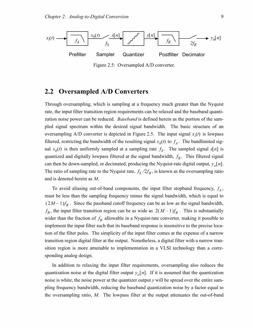
2.2 Oversampled A/D Converters
Through oversampling, which is sampling at a frequency much greater than the Nyquist
rate, the input filter transition region requirements can be relaxed and the baseband quanti-
zation noise power can be reduced. Baseband is defined herein as the portion of the sam-
pled signal spectrum within the desired signal bandwidth. The basic structure of an
oversampling A/D converter is depicted in Figure 2.5. The input signal is lowpass
filtered, restricting the bandwidth of the resulting signal to . The bandlimited sig-
nal is then uniformly sampled at a sampling rate . The sampled signal x[n] is
quantized and digitally lowpass filtered at the signal bandwidth, . This filtered signal
can then be down-sampled, or decimated, producing the Nyquist-rate digital output, [n].
The ratio of sampling rate to the Nyquist rate, , is known as the oversampling ratio
and is denoted herein as M.
To avoid aliasing out-of-band components, the input filter stopband frequency, ,
must be less than the sampling frequency minus the signal bandwidth, which is equal to
. Since the passband cutoff frequency can be as low as the signal bandwidth,
, the input filter transition region can be as wide as . This is substantially
wider than the fraction of allowable in a Nyquist-rate converter, making it possible to
implement the input filter such that its baseband response is insensitive to the precise loca-
tion of the filter poles. The simplicity of the input filter comes at the expense of a narrow
transition region digital filter at the output. Nonetheless, a digital filter with a narrow tran-
sition region is more amenable to implementation in a VLSI technology than a corre-
sponding analog design.
In addition to relaxing the input filter requirements, oversampling also reduces the
quantization noise at the digital filter output [n]. If it is assumed that the quantization
noise is white, the noise power at the quantizer output y will be spread over the entire sam-
pling frequency bandwidth, reducing the baseband quantization noise by a factor equal to
the oversampling ratio, M. The lowpass filter at the output attenuates the out-of-band
fAxi(t)
xb(t) x[n] y[n]
Prefilter Sampler Quantizer
fSfB
Postfilter Decimator
2fB
yo[n]
Figure 2.5: Oversampled A/D converter.
xi t( )
xb t( ) fA
xb t( ) fS
fB
yo
fS 2fB⁄
fA
2M 1–( )fBfB 2 M 1–( )fB
fB
yo
Chapter 2: Analog-to-Digital Conversion 10
noise components, leaving only the baseband noise. Using the standard quantizer, the
dynamic range is then
(2.6)
and is a factor of M larger than the dynamic range of a Nyquist-rate converter with the
same quantizer resolution. Even greater improvements can be attained through the use of
feedback.
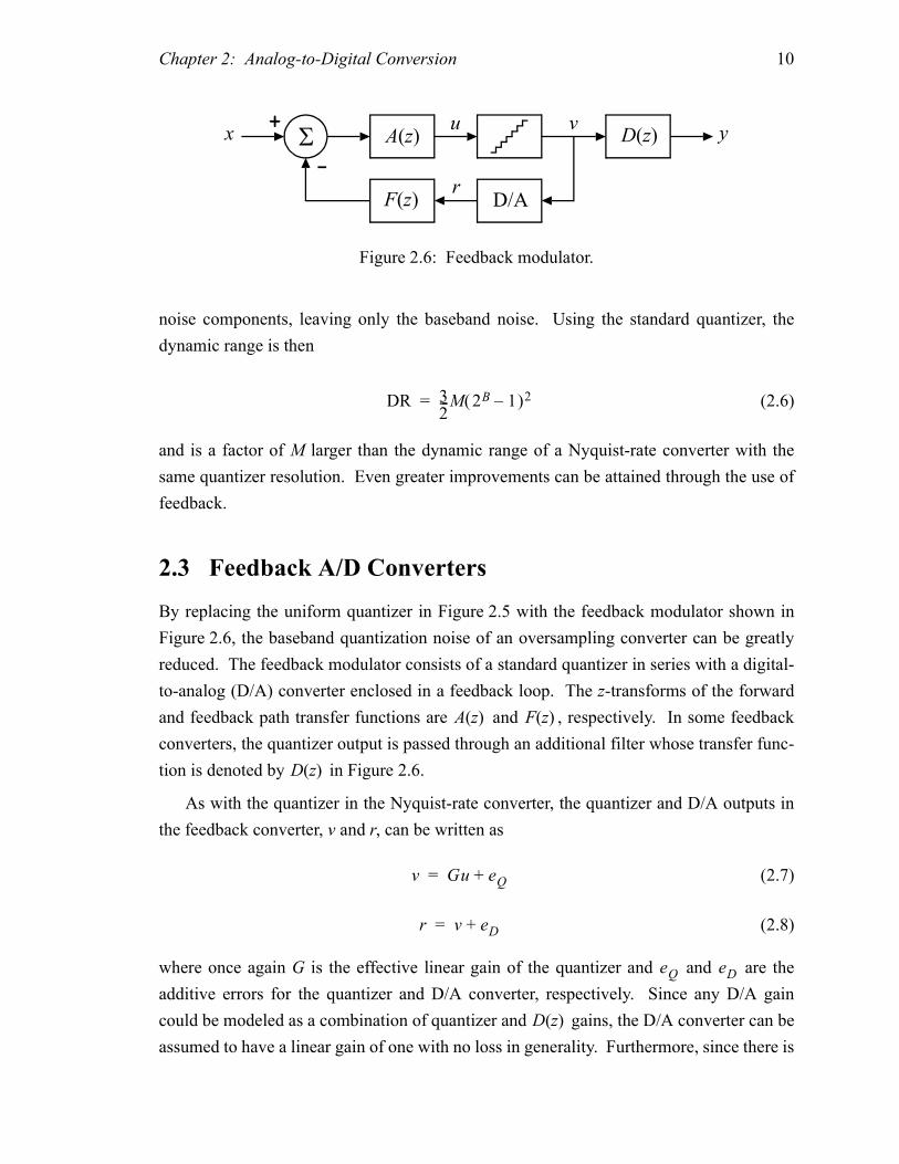
2.3 Feedback A/D Converters
By replacing the uniform quantizer in Figure 2.5 with the feedback modulator shown in
Figure 2.6, the baseband quantization noise of an oversampling converter can be greatly
reduced. The feedback modulator consists of a standard quantizer in series with a digital-
to-analog (D/A) converter enclosed in a feedback loop. The z-transforms of the forward
and feedback path transfer functions are and , respectively. In some feedback
converters, the quantizer output is passed through an additional filter whose transfer func-
tion is denoted by in Figure 2.6.
As with the quantizer in the Nyquist-rate converter, the quantizer and D/A outputs in
the feedback converter, v and r, can be written as
(2.7)
(2.8)
where once again G is the effective linear gain of the quantizer and and are the
additive errors for the quantizer and D/A converter, respectively. Since any D/A gain
could be modeled as a combination of quantizer and gains, the D/A converter can be
assumed to have a linear gain of one with no loss in generality. Furthermore, since there is
DR 32---M 2B 1–( )2=
A(z)
-
+
F(z) D/A
Σx yvu
D(z)
Figure 2.6: Feedback modulator.
r
A z( ) F z( )
D z( )
v Gu eQ+=
r v eD+=
eQ eD
D z( )
Chapter 2: Analog-to-Digital Conversion 11
no additional quantization in the D/A converter, it does not have an inherent noise compo-
nent; the D/A error results solely from implementation non-idealities.
While feedback modulators are often implemented using a single-bit quantizer, the fol-
lowing analysis assumes that the quantizer has many quantization levels so that the gain G
is well defined. Then, as a rough approximation, the analytical results are extrapolated to
the single-bit case. In Chapter 3, an alternative method for analyzing single-bit modula-
tors will be presented.
The purpose of all feedback modulators is to measure the input x while using the base-
band loop gain of the modulator to reduce the quantization error . With the definitions
in (2.7) and (2.8), the modulator output is
(2.9)
where
(2.10)
(2.11)
and , , , and are the z-transforms of x, y, , and , respectively.
The z-transform is related to the frequency domain response by the transformation
(2.12)
In the baseband, , so . In a feedback modulator, the baseband loop gain and
input transfer function are normally designed to satisfy
(2.13)
(2.14)
so that the baseband modulator output, neglecting delays, reduces to
(2.15)
The feedback and forward gains, and , are chosen such that the baseband error
power resulting from the quantizer is small relative to the signal power. If the D/A error
term is also small, the output will be approximately equal to the input. Two basic
approaches to selecting and have been used: prediction and noise shaping.
eQ
Y z( ) Hx z( ) X z( ) F z( )ED z( )–[ ] He z( )EQ z( )+=
Hx z( )GA z( )D z( )
1 GA z( )F z( )+----------------------------------=
He z( )D z( )
1 GA z( )F z( )+----------------------------------=
X z( ) Y z( ) ED z( ) EQ z( ) eD eQ
z e j2πf fS⁄ .=
f << fS z 1≈
GA z( )F z( ) >> 1, z 1≈
H z( )
F z( )---------- 1, z 1≈ ≈
Y z( ) X z( ) F z( )ED z( )1
GA z( )--------------EQ z( ), z 1.≈+–≈
F z( ) GA z( )
F z( ) GA z( )

Chapter 2: Analog-to-Digital Conversion 12
In predictive or delta modulators, the baseband forward gain, , is unity and the
feedback filter, , is designed to predict the input x [15, 16, 17]. If the predicted value
is close to the input value, the signal level at the quantizer input u will be small compared
to the signal level at the input x. This reduces the required quantizer range, ∆. For a
uniform quantizer with a fixed number of bits, a reduction in ∆ also reduces the quantizer
step size, δ, which in turn reduces the error power at the output. The principle disadvan-
tage to this approach is the presence of the D/A converter error, . In general, the pre-
dicting filter has a large baseband gain, and, according to (2.15), this gain greatly
amplifies .
In contrast to predictive modulators, noise-shaping or sigma-delta modulators have a
baseband feedback gain, , of unity and a baseband forward gain, , that is much
greater than one [18]. According to (2.15), a large forward gain reduces the baseband
quantization noise appearing at the output. More precisely, the noise is spectrally shaped
such that the noise energy is concentrated outside the signal band and can be attenuated by
the digital filter at the output. Because of the unity baseband feedback gain, the noise-
shaping technique has the advantage that the D/A error term is not amplified.
A third approach to oversampled modulator design called interpolation uses a combi-
nation of prediction and noise-shaping [19, 20, 21]. Both the baseband feedback gain and
the baseband forward gain are greater than one. Unfortunately, this approach retains the
disadvantage of the predictive modulator in that any D/A converter errors are amplified by
the feedback gain, . Therefore, sigma-delta or noise-shaping modulation, having the
least sensitivity to D/A errors, is the approach used in this work.
While there are many high-gain transfer functions that could be used in a sigma-delta
modulator, one class of transfer functions that is particularly well suited to a VLSI imple-
mentation comprises a linear combination of delaying integrators that differentiate the
quantization noise. The remainder of this chapter is devoted to noise-differencing sigma-
delta modulators.
2.4 Noise-Differencing Sigma-Delta Modulators
The forward path in a noise-differencing sigma-delta modulator consists of a series of
delaying integrators and a standard quantizer enclosed in a feedback loop. The input to
each integrator is the difference between the output of the previous integrator and a scaled
version of the D/A converter output, as shown in Figure 2.7. The order of the modulator
is defined as the number of integrators in the forward path. The forward gain of an L-th
order modulator is
GA z( )
F z( )
eD
F z( )
eD
F z( ) GA z( )
F z( )

Chapter 2: Analog-to-Digital Conversion 13
(2.16)
and the modulator loop gain is
(2.17)
where the transfer function for the delaying integrator is
(2.18)
For the feedback gain, , in the baseband to be approximately unity, must be one.
If (2.16)–(2.18) are substituted into (2.10) and (2.11), the signal and error transfer
functions for the modulator, and , are
(2.19)
(2.20)
For the modulator to be stable, the poles of and must be within the unit circle.
In general, this limits the quantization gain, G. For example, if the feedback terms are
the binomial coefficients, the denominators in (2.19) and (2.20) reduce to
(2.21)
and the modulator is stable if
-
+ +
-
+
-
I(z) I(z) I(z)
b0 b1 bn
x y
D/A
Σ Σ Σ
Figure 2.7: Integrating sigma-delta modulator.
A z( ) I z( )L=
GA z( )F z( ) G bnI z( )L n–
n 0=
L 1–
∑=
I z( )
I z( )z 1–
1 z 1––---------------- .=
F z( ) b0
Hx z( ) He z( )
Hx z( )Gz L–
G bnzn L– 1 z 1––( )n
n 0=
L 1–
∑ 1 z 1––( )L+
---------------------------------------------------------------------------------------=
He z( )1 z 1––( )L
G bnzn L– 1 z 1––( )n
n 0=
L 1–
∑ 1 z 1––( )L+
---------------------------------------------------------------------------------------.=
Hx z( ) He z( )
bn
G 1 G–( ) 1 z 1––( )L+

Chapter 2: Analog-to-Digital Conversion 14
(2.22)
To insure that (2.22) is satisfied and to simplify the mathematics, G is often chosen to be
one.
It follows from (2.15) that the baseband output for an L-th order noise-differencing
sigma-delta modulator, neglecting delays, is
(2.23)
With the white noise approximation, the quantizer noise power in the signal band is
(2.24)
If is neglected and it is assumed that, as in the Nyquist-rate converter, a full-scale sinu-
soidal input has an amplitude of ∆ ⁄ 2G, the dynamic range of a noise-differencing sigma-
delta modulator is
(2.25)
Thus, the dynamic range is proportional to the power of the oversampling ratio, a
tremendous improvement over simple oversampling. Because the dynamic range is such a
strong function of the oversampling ratio, the number of bits required to achieve a given
dynamic range is substantially less in a sigma-delta modulator than in a Nyquist-rate con-
verter. To illustrate this, the dynamic range is shown as a function of the of oversampling
ratio, M, in Figure 2.8 for three combinations of modulator order, L, and quantizer resolu-
tion, B. The equivalent resolution in bits that would be required of a Nyquist-rate con-
verter to achieve the same dynamic range is shown in the right-hand axis of this figure.
It can be inferred from (2.25) that a large dynamic range can be obtained even with
only one bit of resolution in the modulator’s quantizer. One-bit quantization has several
advantages, the most important being that it is inherently uniform. Because there is only
one comparison level and only two output levels, there can be no differential or integral
nonlinearity. Furthermore, the D/A error term at worst introduces a DC offset and gain
error. In many signal processing applications, including the audio-band systems that are
the focus of this work, neither of these D/A errors degrade system performance. With
0 G2L
2L 1–--------------.< <
Y z( ) X z( ) ED z( )1 z 1––( )L
G-----------------------EQ z( ).+–≈
See
σe2
fS------ 1 e j2πf fS⁄––( )L
G-----------------------------------
2df
fB–
fB
∫σe2
G2------
π2L
2L 1+----------------
1
M2L 1+-----------------≈ ≈ .
eD
DR 32--- 2L 1+
π2L---------------- G2M2L 1+ 2B 1–( )2=
2L 1+
eD
Chapter 2: Analog-to-Digital Conversion 15
one-bit quantization, high-resolution performance can then be achieved without precise
component matching.
Unfortunately, a one-bit quantizer in a sigma-delta modulator violates most, if not all,
of the conditions of Bennett’s noise model given in Section 2.1, and the justification for
the white noise approximation is considerably weaker than it is in a multi-bit sigma-delta
modulator. In addition, both the quantizer gain G and the clipping level that was hereto-
fore used to define the maximum input level are undefined. Nonetheless, (2.25) is still a
reasonable approximation for noise-differencing sigma-delta modulators if the quantizer
gain is assumed to be one; this will be referred to as the unity gain approximation.
For the remainder of this chapter, the unity gain approximation will be used to derive
some general properties of noise-differencing modulators. These results will be verified
through computer simulations that use the one-bit quantization function explicitly. In
Chapter 3, an alternative model of one-bit sigma-delta modulators based on the method of
describing functions will be developed.
2.4.1 Considerations in High-Performance Audio
The first step in the design of a noise-differencing sigma-delta modulator is to choose the
modulator order and oversampling ratio. Table 2.1 lists the oversampling ratios required
8 16 32 64 128 256 51260
70
80
90
100
110
120
130
140
10
12
14
16
18
20
22
Oversampling Ratio
Dynamic Range (dB)
Resolution (bits)
L = 2, B = 4
L = 2, B = 1
L = 3, B = 1
Figure 2.8: Calculated dynamic range vs. oversampling ratio.
Chapter 2: Analog-to-Digital Conversion 16
for various combinations of dynamic range and modulator order. These values were cal-
culated for a one-bit quantizer using the unity gain approximation. Although increasing
the modulator order greatly reduces the oversampling ratio required for a given dynamic
range, it also increases the complexity of the modulator and the subsequent decimation fil-
ter.
For a given modulator order, increasing the oversampling ratio reduces both the base-
band quantization noise and the baseband thermal noise produced by the integrator cir-
cuits. Conversely, reducing the oversampling ratio reduces the clock speed required for a
given signal bandwidth. This in turn reduces the integrator speed and slewing require-
ments and the noise generated by the clock edges and coupled through the chip substrate.
All of these effects will be discussed in more detail in later chapters; the point here is that
the choice of oversampling ratio involves a compromise. From both calculations of the
modulator noise performance and empirical evidence from previously published designs,
a target oversampling ratio of 128 was chosen for this work.
According to Table 2.1, achieving a dynamic range of more than 100 dB at an over-
sampling ratio of 128 requires at least a third-order sigma-delta modulator. Unfortunately,
implementation of a third-order modulator is complicated by fact that unstable oscillations
can be excited in modulators employing a single one-bit quantizer with more than two
integrators in the forward path [22]. Various techniques have been used to reduce or elim-
inate the effect of these oscillations while achieving higher-order performance, including
limiting the magnitude of the error transfer function, , at higher frequencies [23, 24,
25], placing limiters at the integrator outputs [26], and cascading lower order modulators
[27, 28, 29].
Cascaded architectures of the form shown in Figure 2.9 have two advantages over
other high-order techniques. First, because stable first- and second-order modulator
Dynamic Range
L 100 dB 110 dB 120 dB
1 2799 6031 12993
2 167 265 419
3 51 71 99
4 27 35 45
Table 2.1: Required oversampling ratios.
He z( )

Chapter 2: Analog-to-Digital Conversion 17
stages can be used to compose a cascaded modulator, no unstable oscillations will be
excited in the modulator as a whole. The second advantage involves noise tones in the
output. In the error spectrum of a single-stage sigma-delta modulator, discrete spectral
peaks or tones can be generated. These tones are most evident in first-order modulators,
have been demonstrated in second- and fourth-order modulators, and are believed to exist
in all single-stage modulators. In a cascaded modulator, the later stages tend to randomize
the noise and eliminate these tones. Noise tones are discussed further in Section 2.6; they
are mentioned here because the motivating factors behind the study of cascaded sigma-
delta modulators were the inherent stability and the improved suppression of noise tones.
2.5 Cascaded Sigma-Delta Modulators
In a cascaded architecture, each of the multiple stages is itself a single-stage sigma-delta
modulator. As depicted in Figure 2.9, the quantizer error in each stage serves as the input
to the following stage. The output of that following stage is then an approximation of the
quantizer error. By subtracting the approximate error from the previous stage’s output,
most of the quantization error can be canceled, and the performance of a cascaded archi-
tecture is approximately equivalent to that of a single-stage architecture having the same
total number of integrators. Instability is avoided because each individual stage is a self-
contained first- or second-order sigma-delta modulator with only one or two integrators in
its forward path.
1st Stage
e1
. . .
2nd Stage
Error Cancellation
e2
xy1
y2 y
Figure 2.9: Cascaded modulator architecture.
Chapter 2: Analog-to-Digital Conversion 18
To concisely differentiate among the various cascade combinations, cascaded modula-
tor topologies will be referred to herein by a sequence of numbers corresponding to the
order of the differential noise shaping provided by each stage in the cascade. The first
number corresponds to the first stage, the second to the second stage, and so on. For
example, a cascade of a first-order stage followed by a second-order stage followed by a
first-order stage would be identified as a 1-2-1 architecture.
In this section, the basic behavior of third-order cascades and the effect of mismatch
among the stages are discussed. Two such architectures for which specific topologies
have been described in the published literature are the 1-1-1 architecture and the
2-1 architecture. Both of these architectures are examined in detail herein. Higher order
cascades could be built, but the performance gains would be minimal due to thermal noise
limitations in the circuit. Even the performance of third-order cascades tends to be limited
by thermal noise in high-resolution applications, as discussed in Chapter 4.
2.5.1 1-1-1 Architecture
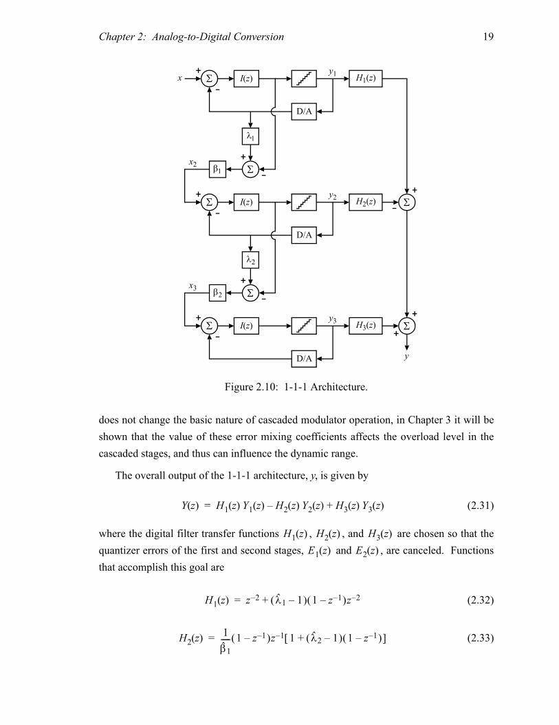
A block diagram of the 1-1-1 architecture is shown in Figure 2.10. It comprises three
first-order modulators coupled through two error mixing networks formed by , , ,
and . The quantized output of each modulator is combined in a digital filtering network
designed to cancel the quantizer errors of the first two stages.
If D/A errors are neglected and it is assumed that either the quantizer has a linear gain
term of unity or that the unity gain approximation holds, the modulator outputs are
(2.26)
(2.27)
(2.28)
where , , and are the z-transforms of the quantizer errors for the first,
second, and third stages, respectively. The inputs to the second and third stages are
(2.29)
(2.30)
where and are the error mixing coefficients and and are the error gain coef-
ficients. Note that if or are not equal to one, the cascaded stage inputs will not be
simply a fraction of the quantizer error as indicated in Figure 2.9. While this modification
β1 λ1 β2
λ2
Y1 z( ) z 1– X z( ) 1 z 1––( )E1 z( )+=
Y2 z( ) z 1– X2 z( ) 1 z 1––( )E2 z( )+=
Y3 z( ) z 1– X3 z( ) 1 z 1––( )E3 z( )+=
E1 z( ) E2 z( ) E3 z( )
X2 z( ) β1 λ1 1–( )Y1 z( ) E1 z( )+[ ]=
X3 z( ) β2 λ2 1–( )Y2 z( ) E2 z( )+[ ]=
λ1 λ2 β1 β2
λ1 λ2
Chapter 2: Analog-to-Digital Conversion 19
does not change the basic nature of cascaded modulator operation, in Chapter 3 it will be
shown that the value of these error mixing coefficients affects the overload level in the
cascaded stages, and thus can influence the dynamic range.
The overall output of the 1-1-1 architecture, y, is given by
(2.31)
where the digital filter transfer functions , , and are chosen so that the
quantizer errors of the first and second stages, and , are canceled. Functions
that accomplish this goal are
(2.32)
(2.33)
-
+
Σ I(z)
D/A
+
-Σ
λ2
β2
-
+
Σ I(z)
D/A
+
-Σ
λ1
β1
-
+
Σ I(z)
D/A
H1(z)
H2(z)
H3(z)
-
+
+
+
Σ
Σ
xy1
y3
y2
x3
x2
y
Figure 2.10: 1-1-1 Architecture.
Y z( ) H1 z( ) Y1 z( ) H2 z( ) Y2 z( ) H3 z( ) Y3 z( )+–=
H1 z( ) H2 z( ) H3 z( )
E1 z( ) E2 z( )
H1 z( ) z 2– λ1 1–( ) 1 z 1––( )z 2–+=
H2 z( )1
β1
----- 1 z 1––( )z 1– 1 λ2 1–( ) 1 z 1––( )+[ ]=

Chapter 2: Analog-to-Digital Conversion 20
(2.34)
where , , , and are the digital estimates of , , , and , respectively.
Since , , , and are analog gains, while , , and are imple-
mented digitally, , , , and will not precisely match , , , and . The
matching errors, represented herein by and , are defined such that
(2.35)
(2.36)
for and 2.
If higher order difference terms are neglected, it follows from equations (2.26)–(2.36)
that the overall output is
(2.37)
From (2.37) it is apparent that if there are no matching errors, the quantizer errors of the
first and second stages are canceled and the only remaining quantizer error term, , is
shaped by a third-order difference similar to that of a third-order single-stage sigma-delta
modulator. With matching errors, fractions of the first- and second-stage quantizer errors,
and , appear at the output, and those quantizer errors are only shaped by first- and
second-order differences, respectively.
Neither and nor the error terms and appear in (2.37). To the extent
that (2.37) is valid, the values of and and errors in those values have no effect on
the output. There are higher order error terms, which have been neglected in (2.37), that
are dependent on and . Nonetheless, the sensitivity to these errors is much less
than that to errors in and .
Simulations of the 1-1-1 architecture reveal that in addition to the and depen-
dence in (2.37), the system parameters , , , and affect both the small signal
quantization noise and the large signal overload level. The combination of parameter val-
ues that represents the best design compromise can be found empirically [30] or by using
the adaptive gain model described in Chapter 3. The unity gain approximation cannot be
used to choose the system parameters because it assumes that the effective quantizer gain
H3 z( )1
β1β2
----------- 1 z 1––( )2=
β1 β2 λ1 λ2 β1 β2 λ1 λ2
β1 β2 λ1 λ2 H1 z( ) H2 z( ) H3 z( )
β1 β2 λ1 λ2 β1 β2 λ1 λ2
δβn δλn
βn βn 1 δβn+( )=
λn λn 1 δ+ λn( )=
n 1=
Y z( )
Y z( ) z 3– X z( ) δβ1 1 z 1––( )z 2– E1 z( )–≈
δβ2
β1
--------+ 1 z 1––( )2z 1– E2 z( )1
β1β2
----------- 1 z 1––( )3E3 z( ).+
e3
e1 e2
λ1 λ2 δλ1 δλ2
λ1 λ2
δλ1 δλ2
β1 β2
β1 β2
β1 β2 λ1 λ2

Chapter 2: Analog-to-Digital Conversion 21
and noise power are constant with respect to the input amplitude and independent of the
system parameters. Nonetheless, the unity gain approximation is still useful in predicting
many aspects of modulator performance, including the effects of matching errors among
the stages.
If it is assumed that the three quantizer error terms in the modulator output are random
and uncorrelated with each other and the input, it follows from (2.37) that the total noise
power in the signal band is
(2.38)
With the unity gain approximation and the assumption that a full-scale sinusoidal input
has an amplitude of ∆ ⁄ 2G, the dynamic range for a 1-1-1 cascade of one-bit stages is
(2.39)
If is defined as the fractional reduction in the dynamic range due to matching
errors, then
(2.40)
If and are of the same order of magnitude, the term will dominate and the
dynamic range reduction is proportional to the fourth power of the oversampling ratio.
Figure 2.11 illustrates the dynamic range reduction versus for an oversampling ratio
of 128 and = = 1. Both simulations that use a one-bit quantization function and
calculations that use (2.40) are shown. For the dynamic range reduction in this example to
be less than 1 dB, the matching error in the first stage must be less than 0.02%. Such a
strict matching requirement defeats much of the purpose of using sigma-delta modulation.
Fortunately, the matching requirements are much less severe in the 2-1 architecture.
2.5.2 2-1 Architecture
A block diagram of the 2-1 architecture is shown in Figure 2.12. It is a cascade of a
second-order modulator followed by a first-order modulator coupled through an error
mixing network formed by and . In a fashion similar to the 1-1-1 architecture, the
See δβ12 π2
3M3----------σe1
2δβ22
β12
--------π4
5M5----------σe2
2 1
β12β2
2------------
π6
7M7----------σe3
2 .+ +≈
DR111 δβ1 δβ2,( ) δβ12 2π2
9M3----------
δβ22
β12
--------2π4
15M5-------------
1
β12β2
2------------
2π6
21M7-------------+ +
1–
.≈
∆S111
∆S111DR111 0 0,( )
DR111 δβ1 δβ2,( )-------------------------------------- 1 β2
27M2
5π2----------δβ2
2 β12β2
27M4
3π4----------δβ1
2 .+ +≈=
δβ1 δβ2 δβ1
δβ1
β1 β2
β λ

Chapter 2: Analog-to-Digital Conversion 22
quantized output of each modulator is combined in a digital filtering network designed to
cancel the quantizer error of the first stage.
Historically, the second-order feedback coefficient b has been chosen to be 2 [22, 31,
32]. This is not necessary, and in certain circumstances is not optimum. The value of b
Figure 2.11: Effect of matching errors in the 1-1-1 architecture.
-2.0 -1.5 -1.0 -0.5 0.0 0.5 1.0 1.5 2.00
5
10
15
20
25
30
35
Matching Error (%)
Loss in Dynamic Range (dB)
u u u u u u u u u uuuuuu
uu
u
u
u u
u
u
uuuuuuuu u
u uu u
u uu u
u Simulated
Calculated
-
+
Σ
y
-
+
Σ I(z)
D/A
-
+
Σ I(z)
D/A
+
-Σ
λ
β
H1(z)
H2(z)
+
y1
y2
x2
-
+
Σ I(z)x
b
Figure 2.12: 2-1 Architecture.
Chapter 2: Analog-to-Digital Conversion 23
affects both the overload level of the modulator and the location and amplitude of spectral
noise tones in the output; these effects are discussed in more detail later in this work. In
this section, however, the unity gain approximation and a b value of 2 will be used for sim-
plicity. This simplification does not alter the results pertaining to the basic operation of
the 2-1 architecture or the effects of matching errors, which are the subjects of this section.
If D/A errors are neglected and it is assumed either that the quantizer has a linear gain
term of unity or that the unity gain approximation holds, the modulator outputs are
(2.41)
(2.42)
where and are the z-transforms of the quantizer errors for the first and second
stages, respectively. The input to the second stage is
(2.43)
where is the error mixing coefficient and is the error gain coefficient. The overall
output of the 2-1 architecture, , is given by
(2.44)
The digital filters and are chosen such that the quantizer error of the first
stage, , is canceled. Functions that accomplish this goal are
(2.45)
(2.46)
where and are the digital estimates of and , respectively.
Since and are analog gains, while and are implemented digitally,
and will not precisely match and . These errors, represented herein by and ,
are defined so that
(2.47)
(2.48)
If higher order difference terms are neglected, it follows from equations (2.41)–(2.48)
that the overall output is
Y1 z( ) z 2– X z( ) 1 z 1––( )2E1 z( )+=
Y2 z( ) z 1– X2 z( ) 1 z 1––( )E2 z( )+=
E1 z( ) E2 z( )
X2 z( ) β λ 1–( )Y1 z( ) E1 z( )+[ ]=
λ β
Y z( )
Y z( ) H1 z( ) Y1 z( ) H2 z( ) Y2 z( ).–=
H1 z( ) H2 z( )
E1 z( )
H1 z( ) z 1– λ 1–( ) 1 z 1––( )2z 1–+=
H2 z( )1
β--- 1 z 1––( )2=
β λ β λ
β λ H1 z( ) H2 z( ) β
λ β λ δβ δλ
β β 1 δβ+( )=
λ λ 1 δ+ λ( ).=
Y z( )
Chapter 2: Analog-to-Digital Conversion 24
(2.49)
From (2.49) it is apparent that if there are no matching errors, then the only remaining
quantizer error term, , is shaped by a third-order difference similar to that of a third-
order single-stage sigma-delta modulator. With matching errors, some of the first-stage
error, , appears at the output, and that error is shaped by a second-order difference.
As with the 1-1-1 architecture, neither nor its error term appear in (2.49). To the
extent that (2.49) is valid, the value of and errors in that value have no effect on the out-
put. There are higher order error terms, which have been neglected in (2.49), that are
dependent on . Nonetheless, the sensitivity to this error is much less than that to errors
in .
As mentioned in the preceding section, β and λ primarily affect the overload level of
the modulator. This effect is not modeled by the unity gain approximation, but is modeled
by the adaptive gain model introduced in Chapter 3.
If the effects of β and λ are neglected and it is assumed that the two error terms in the
modulator output are random and uncorrelated with each other and the input, then it fol-
lows from (2.49) that the total noise power in the baseband is
(2.50)
With the unity gain approximation and the assumption that a full-scale sinusoidal input
has an amplitude of ∆ ⁄ 2G, the dynamic range for a 2-1 cascade of one-bit stages is
(2.51)
If is defined as the fractional reduction in the dynamic range due to matching errors,
then
(2.52)
In the 2-1 architecture, the dynamic range reduction is proportional to the square of the
oversampling ratio. The reduction calculated from (2.52) for an oversampling ratio of 128
and = 0.5 is plotted in Figure 2.13, along with simulation results that use a one-bit quan-
tization function explicitly. For the dynamic range reduction in this example to be less
Y z( ) z 3– X z( ) δβ 1 z 1––( )2z 1– E1 z( )1
β--- 1 z 1––( )3E2 z( )– .–≈
E2 z( )
E1 z( )
λ δλ
λ
δλ
β
See δβ2 π4
5M5----------σe1
2 1
β2-----
π6
7M7----------σe2
2 .+≈
DR21 δβ( ) δβ2 2π4
15M5-------------
1
β2-----
2π6
21M7-------------+
1–.≈
∆S21
∆S21DR21 0( )
DR21 δβ( )---------------------- 1 β27M2
5π2----------δβ
2 .+≈=
β
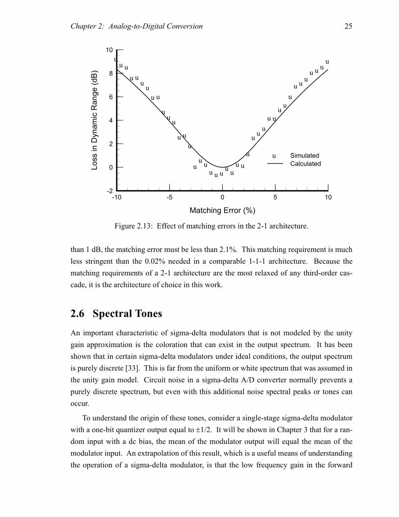
Chapter 2: Analog-to-Digital Conversion 25
than 1 dB, the matching error must be less than 2.1%. This matching requirement is much
less stringent than the 0.02% needed in a comparable 1-1-1 architecture. Because the
matching requirements of a 2-1 architecture are the most relaxed of any third-order cas-
cade, it is the architecture of choice in this work.
2.6 Spectral Tones
An important characteristic of sigma-delta modulators that is not modeled by the unity
gain approximation is the coloration that can exist in the output spectrum. It has been
shown that in certain sigma-delta modulators under ideal conditions, the output spectrum
is purely discrete [33]. This is far from the uniform or white spectrum that was assumed in
the unity gain model. Circuit noise in a sigma-delta A/D converter normally prevents a
purely discrete spectrum, but even with this additional noise spectral peaks or tones can
occur.
To understand the origin of these tones, consider a single-stage sigma-delta modulator
with a one-bit quantizer output equal to ±1/2. It will be shown in Chapter 3 that for a ran-
dom input with a dc bias, the mean of the modulator output will equal the mean of the
modulator input. An extrapolation of this result, which is a useful means of understanding
the operation of a sigma-delta modulator, is that the low frequency gain in the forward
Figure 2.13: Effect of matching errors in the 2-1 architecture.
-10 -5 0 5 10-2
0
2
4
6
8
10
Matching Error (%)
Loss in Dynamic Range (dB)
uu u
u uuu
u u
uuu
u u
u
uuuu u u
uuu u
u
uuu
u u
uu
u
u uuu u
uu
u Simulated
Calculated

Chapter 2: Analog-to-Digital Conversion 26
path of the modulator causes the running average of the output to equal the running
average of the input. For example, with a dc input of 0.0005, the quantizer output will be
a sequence of +0.5 and –0.5’s, such that the average output is 0.0005.
One possible sequence of +0.5 and –0.5’s whose average is 0.0005 is shown in
Figure 2.14a. The output consists of a stream of alternating +0.5 and –0.5’s, except that
every 1000 clock cycles an extra +0.5 is output. The two cycle running average of this
output is shown in Figure 2.14b. For the most part, this running average is zero, except
that at every 1000 clock cycles there is a one clock cycle pulse. This repetitive pulse pro-
duces a tone in the output spectrum at a frequency of
(2.53)
If the oversampling ratio M is less than 500, this tone will appear in the baseband spec-
trum.
In actual sigma-delta modulators, the output sequence is typically more complex than
that illustrated in Figure 2.14. Nonetheless, the concept underlying baseband tones is that
a repeating pattern in the one-bit output whose frequency is within the baseband causes
coloration in the output spectrum. Examples of these tones for a second-order modulator
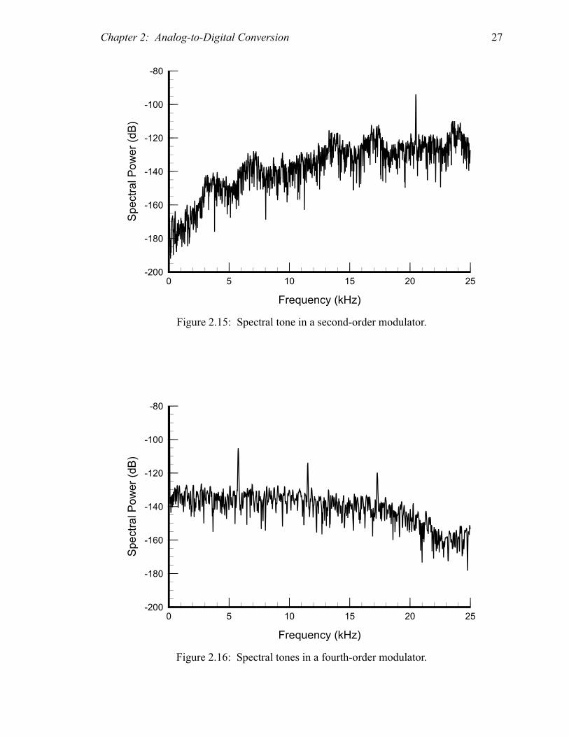
(b = 2.5, x = 0.16560) and a fourth-order modulator (architecture in [23], x = 0.00045) are
shown in Figures 2.15 and 2.16, respectively.
1000 T
T1000 T
(a)
(b)
+0.5
–0.5
+0.5
0
Figure 2.14: (a) Output sequence with average of 0.0005.
(b) Running average of (a).
fP1
1000T---------------
M
500--------- fB.= =
Chapter 2: Analog-to-Digital Conversion 27
Figure 2.15: Spectral tone in a second-order modulator.
0 5 10 15 20 25-200
-180
-160
-140
-120
-100
-80
Frequency (kHz)
Spectral Power (dB)
0 5 10 15 20 25-200
-180
-160
-140
-120
-100
-80
Frequency (kHz)
Spectral Power (dB)
Figure 2.16: Spectral tones in a fourth-order modulator.
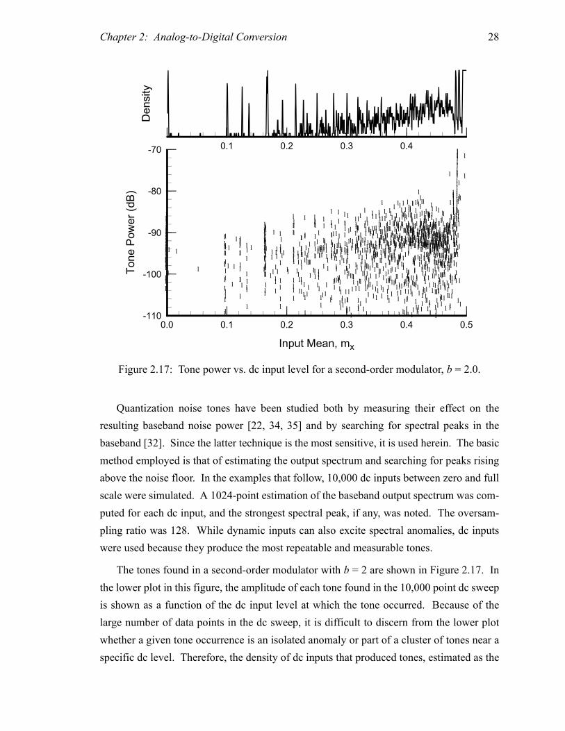
Chapter 2: Analog-to-Digital Conversion 28
Quantization noise tones have been studied both by measuring their effect on the
resulting baseband noise power [22, 34, 35] and by searching for spectral peaks in the
baseband [32]. Since the latter technique is the most sensitive, it is used herein. The basic
method employed is that of estimating the output spectrum and searching for peaks rising
above the noise floor. In the examples that follow, 10,000 dc inputs between zero and full
scale were simulated. A 1024-point estimation of the baseband output spectrum was com-
puted for each dc input, and the strongest spectral peak, if any, was noted. The oversam-
pling ratio was 128. While dynamic inputs can also excite spectral anomalies, dc inputs
were used because they produce the most repeatable and measurable tones.
The tones found in a second-order modulator with b = 2 are shown in Figure 2.17. In
the lower plot in this figure, the amplitude of each tone found in the 10,000 point dc sweep
is shown as a function of the dc input level at which the tone occurred. Because of the
large number of data points in the dc sweep, it is difficult to discern from the lower plot
whether a given tone occurrence is an isolated anomaly or part of a cluster of tones near a
specific dc level. Therefore, the density of dc inputs that produced tones, estimated as the
Figure 2.17: Tone power vs. dc input level for a second-order modulator, b = 2.0.
0.1 0.2 0.3 0.4Density
0.0 0.1 0.2 0.3 0.4 0.5-110
-100
-90
-80
-70
Input Mean, mx
Tone Power (dB)
l
lll
llllllllllllllllllll
l
l l
l
ll
ll
ll
l
l
l
ll
ll
ll
l
lll
l
l
l
l
l
l ll
l
l
l
l
l
l
l
ll
l l
l
l
l
l
l
l
l l
l
lll
llllll
ll
l
ll
l
l
l
ll
ll
l
l
l
ll
llll
lllll
lll
l
l
l
ll
l
l
ll
l
l
lll
l
l
l
l
l
ll
l
lll
ll
ll
l
ll
ll
l
l
l
l
l
lll
lll
l
lll
ll
l
ll
l
l
l
l
l
l
l
l
l
l
l
l
l
l
l
l
l
l
l
l
l
ll
l
ll
l
ll
l
l
ll
lll
l
l
ll
ll
l
ll
l
l
lll
lll
l
l
lllll
ll
llll
l
l
l
l
ll
l
ll
l
ll
l
ll
l
l
l
l
l
ll
l
l
l
ll
ll
l
l
l
l
ll
ll
l
ll
l
l
l
l
l
l
l
lll
l
l
l
ll
l
l
l
l
l
l
l
l
ll
l
l
lll
l
lll
l
l
l
l
l
l
l
ll
l
ll
l
l
l
ll
ll
l
l
l
l
l
l
l
l
lll
l
l
l
l
l
l
l
l
l
l
l
l
l
ll
lll
l
l
l
l
l
l
l
l
l
ll
ll
l
l
l
l
ll
l
l
ll
l
l
l
l
l
l
l
l
ll
l
l
l
l
l
l
l
l
ll
llll
l
l
l
l
l
l
l
l
l
l
l
l
l
l
l
l
ll
l
l
l
l
l
ll
l
l
l
l
l
ll
l
l
l
ll
l
ll
l
l
l
l
l
l
lll
l
l
l
l
l
l
l
l
l
l
l
l
l
lll
l
lllll
l
l
ll
l
l
l
l
l
ll
l
l
ll
l
l
l
l
l
l
l
l
ll
ll
l
l
llll
l
ll
l
l
lll
l
l
l
l
ll
l
l
lll
l
l
l
l
l
l
l
l
l
l
l
ll
l
l
l
l
ll
l
l
l
ll
l
ll
l
lll
l
ll
l
l
l
l
l
l
l
l
l
l
l
l
ll
l
l
l
l
l
l
ll
l
l
l
ll
l
l
l
l
l
l
l
l
ll
l
l
l
l
ll
l
l
ll
l
l
l
l
lll
l
l
l
l
l
l
l
ll
l
l
l
l
l
ll
l
l
l
ll
l
l
l
l
l
l
l
l
l
ll
l
l
ll
l
l
l
l
l
ll
l
l
ll
l
l
l
l
l
l
l
l
l
l
lll
l
l
l
l
l
l
l
ll
l
l
l
l
l
l
l
l
l
l
l
lll
l
l
l
l
l
l
l
l
ll
l
l
ll
l
l
l
ll
l
l
l
ll
l
l
l
l
l
l
ll
ll
l
l
l
l
l
l
l
l
l
l
l
l
l
l
l
l
l
l
l
l
l
l
llll
l
ll
l
l
l
ll
l
l
l
ll
l
l
l
l
ll
l
ll
l
l
l
l
l
l
l
l
l
l
llll
l
l
l
lll
l
l
l
l
l
l
l
l
l
ll
l
l
l
l
l
l
l
l
l
l
l
l
l
l
l
l
l
l
l
l
l
l
l
l
l
ll
l
l
ll
l
l
l
ll
l
l
l
lll
l
l
l
ll
l
lll
l
l
ll
l
l
l
l
l
l
l
l
llll
l
ll
ll
l
l
llll
l
l
l
l
l
l
l
l
l
l
l
l
l
l
l
ll
l
l
l
l
ll
l
lll
l
ll
l
l
l
l
ll
l
l
l
l
l
l
l
ll
l
lll
ll
l
l
l
l
lll
l
l
l
l
ll
l
l
l
l
l
l
l
l
l
l
l
l
l
ll
l
l
l
l
l
l
l
lll
ll
ll
l
l
l
l
l
l
l
l
l
l
l
l
l
l
ll
l
l
l
ll
l
l
ll
l
ll
l
l
l
ll
l
l
l
l
l
l
ll
ll
l
l
l
l
l
l
l
lll
l
l
lllll
l
l
l
lll
l
ll
ll
l
l
ll
l
ll
l
l
ll
ll
l
l
l
l
l
l
l
l
llll
l
l
l
l
l
l
l
l
l
lll
l
l
l
l
lll
l
l
l
l
l
ll
l
l
l
l
l
l
l
l
l
l
l
l
ll
l
l
l
l
ll
ll
l
l
ll
l
l
l
l
l
ll
l
l
lll
l
l
l
l
l
l
l
lll
ll
l
l
l
l
l
ll
ll
l
l
l
l
l
l
ll
l
llll
l
ll
l
ll
l
l
l
l
l
l
l
lllll
l
l
l
l
lll
l
l
l
l
l
l
l
l
lll
l
l
l
l
l
l
l
l
ll
llll
ll
ll
l
ll
l
l
llll
l
l
l
l
l
l
l
l
l
l
l
ll
l
ll
l
l
l
ll
l
l
l
l
l
l
l
ll
l
l
l
l
l
lll
l
l
l
l
l
ll
ll
l
l
l
l
ll
l
l
ll
l
ll
llllllllllllll
lll
l
l
ll
lllll
ll
l
l
l
l
l
l
l
l
l
l
l
l
l
l
l
l
l
l
l
l
l
ll
llll
ll
lll
llllllllllllllll
l
lllllll
ll
l
l
l
lll
l
l
l
l
l
l
l
l
l
l
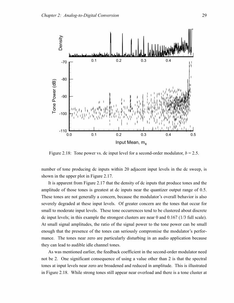
Chapter 2: Analog-to-Digital Conversion 29
number of tone producing dc inputs within 20 adjacent input levels in the dc sweep, is
shown in the upper plot in Figure 2.17.
It is apparent from Figure 2.17 that the density of dc inputs that produce tones and the
amplitude of those tones is greatest at dc inputs near the quantizer output range of 0.5.
These tones are not generally a concern, because the modulator’s overall behavior is also
severely degraded at these input levels. Of greater concern are the tones that occur for
small to moderate input levels. These tone occurrences tend to be clustered about discrete
dc input levels; in this example the strongest clusters are near 0 and 0.167 (1/3 full scale).
At small signal amplitudes, the ratio of the signal power to the tone power can be small
enough that the presence of the tones can seriously compromise the modulator’s perfor-
mance. The tones near zero are particularly disturbing in an audio application because
they can lead to audible idle channel tones.
As was mentioned earlier, the feedback coefficient in the second-order modulator need
not be 2. One significant consequence of using a value other than 2 is that the spectral
tones at input levels near zero are broadened and reduced in amplitude. This is illustrated
in Figure 2.18. While strong tones still appear near overload and there is a tone cluster at
Figure 2.18: Tone power vs. dc input level for a second-order modulator, b = 2.5.
0.1 0.2 0.3 0.4Density
0.0 0.1 0.2 0.3 0.4 0.5-110
-100
-90
-80
-70
Input Mean, mx
Tone Power (dB)
l
lll
l
ll
l
l
l
l
ll
l
ll
l
ll
l
ll
llll
ll
ll
l
ll
l
ll
ll
l
ll
l
l
l
ll
l
llll
l
ll
l
l
l
l
l
l
l
l
l
ll
ll
lll
lll
l
l
lll
ll
ll
l
ll
l
llll
lllllllllll
lll
l
ll
l
l
ll
lll
ll
llllll
l
l
l
lll
l
ll
l
l
ll
ll
l
l
ll
ll
lll
l
ll
lll
ll
l
ll
ll
l
l
l
l
l
l
ll
ll
ll
l
l
l
ll
lll
l
lll
ll
ll
l
l
ll
l
l
l
ll
l
lll
ll
ll
ll
l
ll
l
lll
l
l
l
l
l
l
l
l
l
l
l
ll
l
l
l
l
l
l
l
l
l
l
l
l
l
l
l
l
lll
l
lll
ll
ll
ll
l
l
ll
l
l
l
l
l
ll
l
lll
l
l
ll
l
l
l
ll
l
l
l
l
l
l
l
l
l
l
l
l
l
ll
l
l
l
l
l
l
l
l
lll
l
l
ll
l
ll
ll
l
l
l
l
l
l
l
ll
l
l
lll
l
l
l
l
l
l
l
l
l
l
l
ll
ll
l
ll
l
l
l
l
l
l
l
l
l
l
l
l
l
l
l
l
l
l
l
l
ll
l
l
ll
l
l
l
l
l
l
l
l
ll
l
l
lll
l
l
l
l
l
l
l
l
ll
l
l
l
ll
l
l
l
l
l
l
l
l
l
l
ll
l
l
l
l
l
l
l
l
l
l
l
l
l
l
l
l
l
l
l
l
l
l
l
ll
l
l
l
ll
l
l
l
ll
l
l
l
l
l
l
l
l
l
l
ll
l
lll
l
l
l
l
ll
l
l
l
l
l
l
ll
ll
l
ll
l
ll
lll
l
l
l
l
l
l
l
l
l
ll
ll
l
l
l
l
l
l
l
l
l
l
l
l
l
l
l
l
l
l
l
l
l
l
l
ll
ll
ll
l
ll
l
l
l
l
l
l
l
l
l
ll
l
l
lll
l
l
l
l
ll
l
l
l
ll
l
ll
l
l
l
l
l
ll
l
l
ll
l
l
l
l
l
l
l
l
l
ll
l
l
ll
l
l
l
l
l
l
l
l
l
l
lll
llll
l
l
l
l
l
l
l
l
l
l
l
lll
lll
l
l
l
l
l
l
l
l
l
ll
l
l
lll
l
l
l
lll
l
l
l
l
l
l
l
l
l
l
l
l
l
l
ll
l
ll
l
l
l
l
l
l
l
l
l
l
l
l
l
l
lll
l
l
l
l
lll
lll
l
l
l
ll
l
l
l
ll
ll
l
l
l
l
lll
l
l
l
l
l
l
l
l
l
l
l
lll
l
l
l
ll
l
l
l
l
l
l
ll
l
l
l
l
ll
l
ll
l
l
ll
l
l
l
l
l
l
l
l
l
l
l
l
l
l
ll
l
l
l
l
l
lllll
ll
l
l
l
l
l
l
l
l
llllll
l
lll
l
l
l
l
l
l
l
l
l
l
ll
l
ll
l
l
l
l
l
l
l
l
l
l
l
l
ll
l
l
ll
l
l
ll
l
l
l
l
l
l
llllll
lllll
l
lllll
lll
l
lll
lll
llll
l
l
l
l
lllll
l
ll
l
ll
l
ll
l
lllllll
l
l
lllll
llllllllllllllllllllll
l
l
l
l
l
ll
l
l
l
l
l
l
l
l
l
l
l
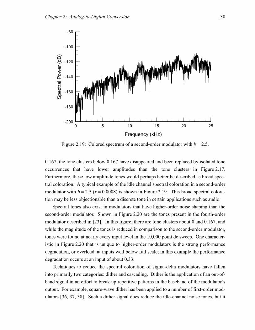
Chapter 2: Analog-to-Digital Conversion 30
0.167, the tone clusters below 0.167 have disappeared and been replaced by isolated tone
occurrences that have lower amplitudes than the tone clusters in Figure 2.17.
Furthermore, these low amplitude tones would perhaps better be described as broad spec-
tral coloration. A typical example of the idle channel spectral coloration in a second-order
modulator with b = 2.5 (x = 0.0008) is shown in Figure 2.19. This broad spectral colora-
tion may be less objectionable than a discrete tone in certain applications such as audio.
Spectral tones also exist in modulators that have higher-order noise shaping than the
second-order modulator. Shown in Figure 2.20 are the tones present in the fourth-order
modulator described in [23]. In this figure, there are tone clusters about 0 and 0.167, and
while the magnitude of the tones is reduced in comparison to the second-order modulator,
tones were found at nearly every input level in the 10,000 point dc sweep. One character-
istic in Figure 2.20 that is unique to higher-order modulators is the strong performance
degradation, or overload, at inputs well below full scale; in this example the performance
degradation occurs at an input of about 0.33.
Techniques to reduce the spectral coloration of sigma-delta modulators have fallen
into primarily two categories: dither and cascading. Dither is the application of an out-of-
band signal in an effort to break up repetitive patterns in the baseband of the modulator’s
output. For example, square-wave dither has been applied to a number of first-order mod-
ulators [36, 37, 38]. Such a dither signal does reduce the idle-channel noise tones, but it
0 5 10 15 20 25-200
-180
-160
-140
-120
-100
-80
Frequency (kHz)
Spectral Power (dB)
Figure 2.19: Colored spectrum of a second-order modulator with b = 2.5.

Chapter 2: Analog-to-Digital Conversion 31
has been shown that the tones are simply shifted and occur for different dc inputs [2]. As
discussed earlier in this section, the same effect in a second-order modulator can be
achieved by simply changing the feedback coefficient from 2.0 to 2.5. A more effective
means of eliminating noise tones is to use a cascaded architecture.
In a cascaded modulator, the successive stages tend to randomize the quantization
error, and the quantization error of the final stage approaches being white noise [35, 39].
If the quantization error from the previous stages is completely canceled, the coloration in
the output from the first stage is eliminated. This is illustrated in Figure 2.21, where a
spectral tone that was present in the second-order modulator is reduced by at least 50 dB
in the 2-1 architecture. However, the caveat that the error cancellation be complete is
important. As the analysis in the previous section indicated, if there is any parameter mis-
match the quantizer error from the first stage of the cascade will leak though to the output.
Any first-stage error appearing at the output will include the tones from the first-stage
error spectrum. This effect is quite pronounced in the 1-1-1 architecture because of the
strong tones present in a first-order modulator. In a 2-1 architecture, the tones in the first
stage are much weaker than those in the first stage of a 1-1-1 architecture. Consequently,
Overload Region
Figure 2.20: Tone power vs. dc input level for a fourth-order modulator.
0.0 0.1 0.2 0.3 0.4 0.5-120
-110
-100
-90
-80
-70
Input Mean, mx
Tone Power (dB)
llllllllllllllllllllllllllllll
l
l
l
ll
lll
ll
lll
l
l
l
l
l
l
l
lll
ll
ll
ll
l
ll
l
l
l
l
l
l
lll
l
l
l
llllll
l
lllllll
l
l
l
l
llllll
l
l
lll
l
l
l
l
ll
ll
ll
ll
l
l
lll
l
l
l
l
lll
l
lll
ll
l
lll
l
l
ll
l
ll
l
l
ll
l
l
ll
l
l
l
l
l
lllll
l
l
l
l
l
l
l
l
ll
l
l
lll
l
ll
l
ll
l
ll
l
lll
l
l
ll
l
lll
l
lll
l
l
ll
ll
lllll
llll
l
l
l
lllllll
llll
l
llllll
llll
ll
llll
l
lll
l
l
llllll
l
ll
ll
lllllll
l
l
l
ll
l
ll
l
l
l
ll
l
ll
l
l
l
ll
lll
ll
l
l
l
l
llllll
l
lll
l
l
lll
ll
ll
lll
ll
lll
l
l
lll
lll
ll
l
l
l
l
l
lll
lll
ll
lllllllll
l
lll
ll
l
l
llll
ll
llll
l
l
llllll
l
l
llll
l
l
ll
l
l
l
lllll
lll
l
lll
lll
l
l
l
l
l
l
l
l
l
ll
l
l
l
l
l
l
lllll
ll
lll
l
l
l
ll
l
l
lll
l
l
llll
l
ll
l
l
l
ll
l
ll
l
lll
ll
l
llllll
l
l
l
lllll
l
l
l
l
l
l
l
ll
ll
l
ll
lllll
ll
llll
ll
l
lll
l
ll
l
l
lll
lll
llll
l
l
lll
ll
l
llll
l
ll
l
ll
l
llll
l
l
ll
l
l
lll
ll
l
l
l
llll
l
lll
l
ll
ll
l
llllll
l
l
l
l
l
lll
l
l
l
l
l
l
l
l
ll
ll
l
ll
llll
l
lll
l
l
l
ll
l
ll
ll
l
l
l
lll
l
llll
ll
lllll
l
l
lll
ll
ll
llll
l
l
ll
lll
lll
ll
l
l
lllll
ll
l
ll
l
l
ll
l
l
l
ll
l
l
l
ll
ll
l
llll
l
ll
l
ll
l
l
l
ll
l
l
l
l
l
l
l
l
l
lll
l
l
l
lll
ll
l
l
l
l
ll
lllll
l
l
ll
llllll
ll
l
l
l
l
lll
ll
l
l
l
ll
l
ll
l
ll
ll
l
l
l
ll
l
l
lll
llll
l
l
l
l
ll
l
l
l
l
llll
l
l
l
l
l
ll
lll
ll
l
llll
l
l
l
l
l
l
l
ll
l
ll
l
l
l
l
l
lll
l
ll
l
l
lll
l
l
ll
l
l
l
l
l
l
l
l
l
lll
ll
l
l
l
ll
lllll
ll
l
l
lll
l
llllll
l
l
l
lllll
l
l
l
ll
ll
ll
l
l
l
l
llllll
l
lll
l
l
l
ll
ll
l
l
llll
l
l
lll
l
l
lll
ll
ll
ll
l
l
l
l
l
l
ll
l
l
l
ll
ll
l
ll
llll
l
l
llll
ll
l
l
ll
ll
l
l
l
l
ll
l
l
lll
ll
lll
l
lll
l
l
ll
lllll
lll
ll
l
l
l
ll
l
l
l
lll
l
ll
l
l
l
l
ll
l
l
l
l
l
lll
lll
l
lll
ll
ll
lll
lll
l
lll
l
l
l
lll
l
l
l
l
l
l
l
lllllllllllllllll
l
l
llllllllllll
lllll
l
l
ll
lllll
l
llll
lll
ll
l
l
l
ll
ll
l
ll
ll
ll
l
lll
l
llll
l
l
l
l
l
l
l
l
l
l
l
l
lll
l
l
l
l
lllllll
lll
ll
l
lll
lllllll
ll
ll
l
l
l
l
l
ll
l
l
lll
llll
l
l
l
l
lll
lll
l
lll
l
l
l
lll
lll
l
llllll
l
l
ll
l
ll
l
ll
lll
l
l
l
l
ll
l
l
l
l
lll
ll
ll
lllll
llllll
l
l
lll
ll
l
llll
l
l
l
ll
lll
lll
l
l
llllll
l
l
lll
l
l
ll
ll
l
l
l
l
l
l
l
l
ll
l
l
l
l
ll
l
ll
l
l
l
ll
l
l
l
ll
l
l
l
lll
lll
l
l
l
lll
l
lllll
l
l
l
ll
l
llll
l
l
ll
lll
l
l
l
l
llll
l
l
l
ll
l
l
l
l
lll
ll
l
l
l
l
l
ll
l
l
ll
lll
l
l
l
l
ll
l
l
ll
l
ll
l
l
l
ll
l
l
ll
l
l
ll
ll
ll
ll
l
l
l
ll
l
l
ll
l
l
ll
l
l
l
ll
l
ll
l
l
lll
ll
l
l
l
l
l
l
ll
l
ll
ll
ll
l
l
l
l
lll
ll
l
l
l
l
l
l
l
ll
ll
l
llll
l
llll
l
l
llll
l
l
l
ll
ll
l
ll
l
ll
l
ll
l
l
l
l
l
l
l
l
ll
l
lllll
ll
l
l
l
l
ll
lll
ll
l
ll
l
ll
ll
l
l
l
l
l
l
l
l
l
l
lll
l
l
ll
lll
l
ll
l
l
lll
llll
l
l
lll
ll
ll
l
l
llll
l
llll
l
l
lllll
l
ll
l
ll
l
l
ll
llll
l
l
l
lllll
ll
ll
llll
llll
l
ll
ll
l
l
ll
ll
l
l
lll
l
l
l
lll
ll
l
l
l
l
l
l
l
lll
ll
ll
ll
l
l
l
ll
l
l
ll
l
l
ll
l
l
l
l
l
l
l
ll
l
ll
llll
lll
l
ll
ll
l
llll
l
l
l
l
l
llllll
l
l
ll
l
l
l
ll
ll
l
l
l
l
l
l
l
lll
l
lll
l
ll
l
ll
l
l
l
l
ll
ll
ll
ll
l
lll
l
l
l
l
l
l
l
l
llll
lllll
l
lll
l
l
lll
l
l
l
l
ll
ll
l
l
ll
ll
ll
ll
l
l
l
l
ll
ll
l
ll
lll
l
ll
ll
llll
llll
l
ll
ll
l
l
l
l
l
l
l
ll
l
l
lllll
l
lllll
llll
l
l
l
lll
l
l
l
l
l
ll
ll
l
ll
l
l
l
l
l
lll
ll
l
ll
l
ll
l
l
ll
l
l
l
l
l
l
l
l
ll
l
l
l
ll
lll
ll
ll
l
l
ll
l
ll
l
l
l
l
l
l
l
l
ll
ll
l
ll
l
l
l
l
l
ll
l
l
l
l
l
l
ll
l
l
l
lll
ll
l
l
l
ll
l
l
l
l
ll
l
l
l
l
l
l
l
l
l
l
ll
l
l
lll
lll
l
l
lll
l
ll
ll
l
l
l
l
ll
l
l
l
l
lll
l
ll
l
ll
l
llll
l
lll
l
lll
lll
llll
l
l
l
l
l
l
lll
llll
l
l
l
l
l
l
l
ll
l
lllll
l
l
ll
ll
l
l
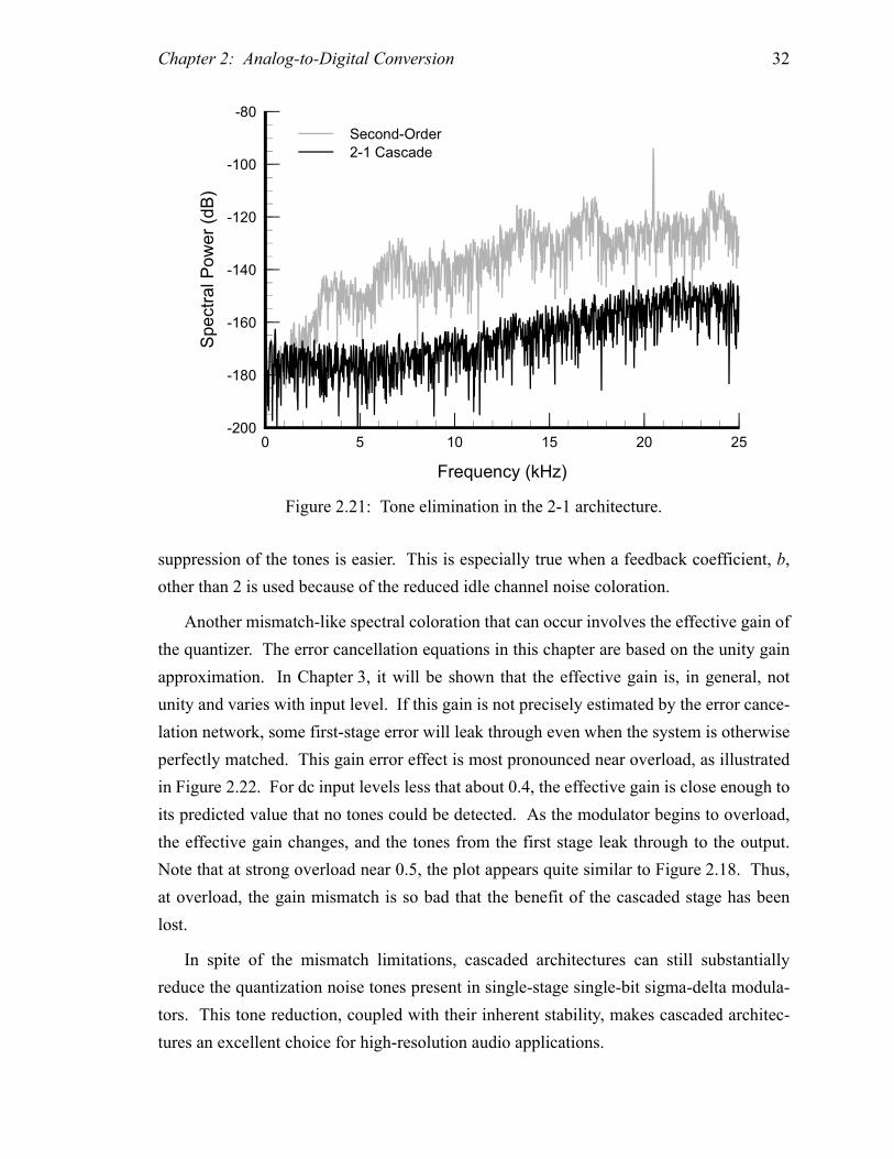
Chapter 2: Analog-to-Digital Conversion 32
suppression of the tones is easier. This is especially true when a feedback coefficient, b,
other than 2 is used because of the reduced idle channel noise coloration.
Another mismatch-like spectral coloration that can occur involves the effective gain of
the quantizer. The error cancellation equations in this chapter are based on the unity gain
approximation. In Chapter 3, it will be shown that the effective gain is, in general, not
unity and varies with input level. If this gain is not precisely estimated by the error cance-
lation network, some first-stage error will leak through even when the system is otherwise
perfectly matched. This gain error effect is most pronounced near overload, as illustrated
in Figure 2.22. For dc input levels less that about 0.4, the effective gain is close enough to
its predicted value that no tones could be detected. As the modulator begins to overload,
the effective gain changes, and the tones from the first stage leak through to the output.
Note that at strong overload near 0.5, the plot appears quite similar to Figure 2.18. Thus,
at overload, the gain mismatch is so bad that the benefit of the cascaded stage has been
lost.
In spite of the mismatch limitations, cascaded architectures can still substantially
reduce the quantization noise tones present in single-stage single-bit sigma-delta modula-
tors. This tone reduction, coupled with their inherent stability, makes cascaded architec-
tures an excellent choice for high-resolution audio applications.
Figure 2.21: Tone elimination in the 2-1 architecture.
0 5 10 15 20 25-200
-180
-160
-140
-120
-100
-80
Frequency (kHz)
Spectral Power (dB)
Second-Order
2-1 Cascade

Chapter 2: Analog-to-Digital Conversion 33
2.7 Summary
In high-resolution integrated circuit A/D converters, the matching requirements of the
more traditional Nyquist-rate converters make their use difficult if not impossible. As an
alternative, A/D converters based on sigma-delta modulation can achieve high-resolution
performance without strict matching requirements through the use of oversampling and
noise shaping, effectively trading speed for resolution. Several sigma-delta architectures
have been presented in this chapter; in a high-resolution audio application, a third-order
modulator represents the best compromise between noise reduction and circuit complex-
ity. Specifically, the cascaded 2-1 architecture achieves stable third-order noise shaping
with the additional benefit of spectral noise tone suppression. In the next chapter, this
architecture will be analyzed in greater detail through the use of the adaptive gain model.
The model will be used to choose the modulator parameters so as to maximize the
dynamic range.
Figure 2.22: Tone power vs. dc input level for the 2-1 architecture.
0.0 0.1 0.2 0.3 0.4 0.5-120
-110
-100
-90
-80
-70
Input Mean, mx
Tone Power (dB)
ll
l
ll
l
llll
l
llll
ll
l
llll
lllll
l
l
l
lll
l
l
l
lll
l
ll
l
ll
lll
l
l
l
l
ll
l
ll
ll
ll
l
l
l
l
l
l
l
l
llll
ll
l
l
l
l
l
l
l
l
l
l
ll
l
l
l
l
l
l
l
l
l
l
l
ll
l
l
l
ll
ll
l
ll
l
l
l
l
l
ll
l
lll
lll
l
l
l
ll
l
l
l
l
l
l
l
ll
l
l
l
lll
l
l
l
l
l
l
l
l
l
l
l
l
l
l
l
l
l
l
l
l
l
l
l
ll
l
l
l
lll
ll
lll
ll
lll
l
l
l
l
l
ll
l
l
l
l
l
l
ll
l
ll
l
l
l
l
l
l
l
l
l
l
l
l
l
l
ll
l
l
lll
l
l
l
l
l
ll
l
l
l
l
l
l
l
l
l
l
l
lllll
l
ll
ll
l
ll
l
l
l
l
l
l
l
l
l
l
l
l
l
l
l
l
l
lll
l
l
l
l
l
ll
l
l
l
l
ll
l
l
l
ll
l
l
l
ll
ll
l
l
l
l
ll
l
l
l
l
l
ll
l
l
l
l
l
l
l
ll
l
ll
lll
l
l
l
l
l
l
l
l
l
l
l
l
l
l
l
ll
l
l
l
l
l
ll
l
ll
l
l
ll
l
l
l
l
l
l
l
l
l
ll
l
l
l
ll
l
l
l
l
l
lllll
ll
l
l
l
l
l
l
l
l
l
lll
l
lll
l
lll
l
l
l
l
l
l
l
l
l
l
l
l
ll
l
l
l
l
l
l
l
l
l
l
l
l
l
ll
l
l
l
ll
l
l
ll
l
l
l
l
l
l
llllll
lllll
l
lllll
lll
l
lll
lll
llll
l
l
l
l
lllll
l
ll
lll
l
ll
l
lllllll
l
l
lllll
llllllllllllllllllllll
l
l
l
l
l
ll
l
l
l
l
l
l
l
l
l
l
l
l
l
l

34
Chapter
3 Adaptive Gain Model
In Chapter 2, each of the uniform quantizers in the analog-to-digital converters was
modeled as a linear gain plus an additive white noise term. This model was loosely based
on Bennett’s noise model which assumed that there were many quantization levels, that
the signal at the input of the quantizer was large relative to the quantization level separa-
tion, that the quantizer input did not exceed the signal range of the quantizer, and that any
two quantizer inputs have a smooth joint probability density. These assumptions are
invalid for single-bit quantizers. Nonetheless, a unity gain approximation was used in
which the quantizer was modeled as a linear gain of one plus an additive white noise term.
This approximation proved to be useful in predicting some basic characteristics of sigma-
delta modulators, such as the dependency of the dynamic range on the oversam-
pling ratio and the effects of mismatches in cascaded architectures. However, it failed to
account for many aspects of single-bit sigma-delta modulator performance, including col-
oration in the noise spectrum and the effect of some system parameters on the small signal
quantization noise and the large signal overload level.
To formulate an accurate description of the quantization noise spectrum, an exact ana-
lytical solution of the sigma-delta modulator has been found for a small but important set
of architectures, including the first-order modulator [40, 41], the second-order modulator
with a two-bit quantizer [42], and first-order cascades [39]. These complex analyses have
led to important discoveries such as the discrete nature of the quantization spectrum in a
first-order modulator and the whitening of the spectrum in cascaded architectures. How-
ever, analysis of the architecture of most interest in this work, the 2-1 architecture, has not
been solved to date.
The difficulty in analyzing one-bit sigma-delta modulators lies in the strong nonlinear-
ity of the quantizer. One classical approach to modeling nonlinear systems is the method
of describing functions [43]. In this approach, the nonlinearity is assumed to have a spe-
cific input, such as a dc bias or sinusoidal input. The nonlinearity is then modeled by a
M2L 1+
Chapter 3: Adaptive Gain Model 35
linear gain chosen to minimize the mean squared error of the approximation. This
approach was extended to systems with random inputs by Booton [44], and adapted for
sigma-delta modulators by Ardalan and Paulos [45]. In this chapter, a variation on the
Ardalan and Paulos approach, termed the adaptive gain model, is introduced.
In the adaptive gain model, a combination of describing function analysis, approxima-
tions, and empirical modeling are used to produce a reasonably accurate estimate of the
signal-to-noise ratio versus the input amplitude, including the effects of system parameters
on the quantization noise and overload characteristics. In the first section of this chapter,
the method of describing functions is briefly introduced and applied to sigma-delta modu-
lators. In Section 3.2, the white noise approximation is defined and results based on this
approximation are derived. Because of this white noise approximation, spectral tones can-
not be modeled using the adaptive gain model. It will be found that estimating the quan-
tizer error variance is an integral part of the adaptive gain model, so in the third section
some properties of the error variance are derived, and an approximate expression for the
error variance is introduced. Finally, in Section 3.4, the adaptive gain model is used to
analyze the 2-1 architecture. While the adaptive gain model could in principle be applied
to any sigma-delta architecture, the 2-1 architecture is studied both because it provides an
illustrative example and because it is the architecture used in the remainder of this work.
3.1 Describing Function Representation
The block diagram for a generalized single-stage sigma-delta modulator is shown in
Figure 3.1. It comprises a one-bit quantizer enclosed in a feedback loop with the z-trans-
forms of the forward and feedback transfer functions being and , respectively.
The one-bit quantizer is represented by the quantization function , where
(3.1)
For simplicity, the quantizer output range, denoted ∆ in Chapter 2, has been chosen to be
one. This simplification affects only the relative scaling of the input.
While the analysis will later be expanded to model sinusoidal inputs, the adaptive gain
model begins by assuming that the modulator input x is a stationary and ergodic random
signal [5] with a mean . Such an input can be thought of as a dc input with an additive
random, but not necessarily white, noise. It is then reasonable to assume that the quantizer
A z( ) F z( )
Q u( )
Q u( )
1
2--, u 0≥
1
2--– , u 0.<
=
mx

Chapter 3: Adaptive Gain Model 36
input u and output y will also be ergodic random signals. With this assumption, the quan-
tizer input u can be split into its mean, , and a zero-mean random signal, , such that
(3.2)
In the method of describing functions, the quantizer is modeled as linear gains for the
dc and random portions of u, denoted herein as K and G respectively. The error in this lin-
earization, hereafter referred to as the quantization error, is then
(3.3)
The gains G and K are chosen to minimize the mean squared error , where is the
time average operator. From (3.3) and the linearity of the time average operator, the mean
squared error is
(3.4)
where and are the variances of u and y, respectively, is the mean of y, and
y = . The second derivatives of with respect to G and K, and , are
necessarily non-negative, so the error is minimized when
(3.5)
By substituting (3.4) into (3.5), the gain values that minimize the error are found to be
(3.6)
(3.7)
mu ur
u ur mu.+=
A(z)
F(z)
Q(u)u
x y+
-
Σ
Figure 3.1: Generalized sigma-delta modulator.
e u( ) Q u( ) Gur Kmu.––=
e2⟨ ⟩ ⟨ ⟩
e2⟨ ⟩ σy2 2G yur⟨ ⟩– G2σu
2 my Kmu–( )2+ +=
σu2 σy
2 my
Q u( ) e2⟨ ⟩ 2σu2 2mu
2
e2⟨ ⟩∂G∂
-------------e2⟨ ⟩∂K∂
------------- 0.= =
Gyur⟨ ⟩
σu2
-------------=
Kmy
mu
------ .=

Chapter 3: Adaptive Gain Model 37
With the gain values given above, the mean and variance of the error are
(3.8)
(3.9)
Because the error mean is zero, the entire modulator can be modeled as a superposition of
a dc bias system and a random system as illustrated in Figure 3.2, where
(3.10)
(3.11)
and and are the means of x and y, respectively. The outputs of the dc and random
systems can then be written as
(3.12)
(3.13)
where
(3.14)
me my Kmu– 0= =
σe2 e2⟨ ⟩ σy
2 G2σu2.–= =
A(z)
F(z)
Σ+
-
A(z)
F(z)
Σ+
-
+
+
++
Σ
Σ
G
K
y
e
ur
mu
yr
my
xr
mx
x
Figure 3.2: Describing function superposition of random and bias systems.
x xr mx+=
y yr my+=
mx my
my Hxm 1( )mx=
Yr z( ) Hx z( )Xr z( ) He z( )E z( )+=
Hxm 1( )KA 1( )
1 KA 1( )F 1( )+-----------------------------------=
Chapter 3: Adaptive Gain Model 38
(3.15)
(3.16)
and , , and are the z-transforms of , , and e, respectively. In the base-
band response of all sigma-delta modulators, that is, for as discussed in Section 2.3,
the magnitude of the loop gain is very large and , so ,
, , and
(3.17)
Since the mean of the output is equal to the mean of the input, one way to view a sigma-
delta modulator is that the low frequency gain in the forward path of the modulator forces
the running average of the output to equal the running average of the input.
In traditional applications of nonlinear describing functions such as control systems,
any error attributed to a given nonlinearity is assumed to be reduced by the system feed-
back loop and is neglected at the input of that nonlinearity. If this approach were applied
to sigma-delta modulators, the gains G and K could be computed given the transfer func-
tions and and the input x. In sigma-delta modulators, however, the quantizer
error forms a significant portion of the quantizer input u and cannot be neglected.
For the describing function analysis to be useful, the nature of the quantizer error must be
understood.
3.2 The White Noise Approximation
For the standard quantizer introduced in Chapter 2, a white noise approximation was used
in which the quantizer error was assumed to be white noise that was uncorrelated with the
input. In this section, it will be shown that, in the context of the adaptive gain model, this
is a reasonable approximation for single-bit sigma-delta modulators. Using this approxi-
mation, the baseband performance of the modulator as a function of the gain G and the
error variance can be determined and a relationship between G and can be derived.
3.2.1 Quantizer Error Power Spectrum
Exact analysis of the first-order modulator [40] and simulations of higher-order modula-
tors indicate that for pure dc inputs ( ), the autocorrelation power spectrum of the
quantizer error is composed of discrete spectral lines. As an example, an estimate of
the error power spectrum of a second-order modulator with and is
Hx z( )GA z( )
1 GA z( )F z( )+----------------------------------=
He z( )1
1 GA z( )F z( )+----------------------------------=
Xr z( ) Yr z( ) E z( ) xr yr
z 1≈
A z( )F z( ) F z( ) 1≈ Hxm 1( ) 1≈
Hx z( ) 1≈ He z( ) << 1
my mx.≈
A z( ) F z( )
e u( )
σe2 σe
2
xr 0=
e u( )
b 2.5= mx 0.11=
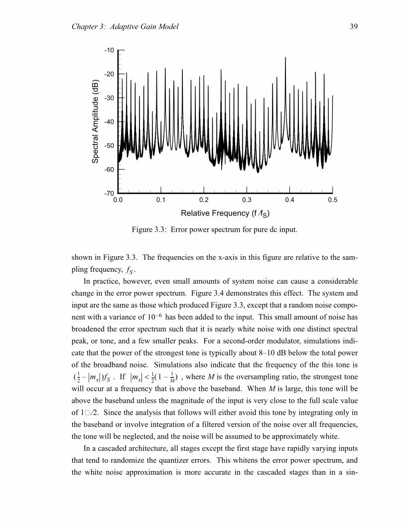
Chapter 3: Adaptive Gain Model 39
shown in Figure 3.3. The frequencies on the x-axis in this figure are relative to the sam-
pling frequency, .
In practice, however, even small amounts of system noise can cause a considerable
change in the error power spectrum. Figure 3.4 demonstrates this effect. The system and
input are the same as those which produced Figure 3.3, except that a random noise compo-
nent with a variance of has been added to the input. This small amount of noise has
broadened the error spectrum such that it is nearly white noise with one distinct spectral
peak, or tone, and a few smaller peaks. For a second-order modulator, simulations indi-
cate that the power of the strongest tone is typically about 8–10 dB below the total power
of the broadband noise. Simulations also indicate that the frequency of the this tone is
. If , where M is the oversampling ratio, the strongest tone
will occur at a frequency that is above the baseband. When M is large, this tone will be
above the baseband unless the magnitude of the input is very close to the full scale value
of 1 ⁄ 2. Since the analysis that follows will either avoid this tone by integrating only in
the baseband or involve integration of a filtered version of the noise over all frequencies,
the tone will be neglected, and the noise will be assumed to be approximately white.
In a cascaded architecture, all stages except the first stage have rapidly varying inputs
that tend to randomize the quantizer errors. This whitens the error power spectrum, and
the white noise approximation is more accurate in the cascaded stages than in a sin-
0.0 0.1 0.2 0.3 0.4 0.5-70
-60
-50
-40
-30
-20
-10
Relative Frequency (f ⁄ fS)
Spectral Amplitude (dB)
Figure 3.3: Error power spectrum for pure dc input.
fS
10 6–
1
2-- mx–( )fS mx
1
2-- 1
1
M---–( )<
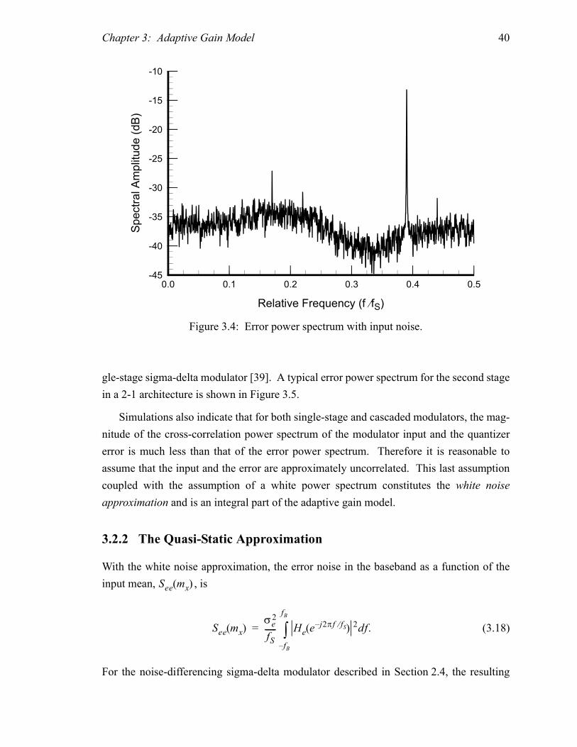
Chapter 3: Adaptive Gain Model 40
gle-stage sigma-delta modulator [39]. A typical error power spectrum for the second stage
in a 2-1 architecture is shown in Figure 3.5.
Simulations also indicate that for both single-stage and cascaded modulators, the mag-
nitude of the cross-correlation power spectrum of the modulator input and the quantizer
error is much less than that of the error power spectrum. Therefore it is reasonable to
assume that the input and the error are approximately uncorrelated. This last assumption
coupled with the assumption of a white power spectrum constitutes the white noise
approximation and is an integral part of the adaptive gain model.
3.2.2 The Quasi-Static Approximation
With the white noise approximation, the error noise in the baseband as a function of the
input mean, , is
(3.18)
For the noise-differencing sigma-delta modulator described in Section 2.4, the resulting
0.0 0.1 0.2 0.3 0.4 0.5-45
-40
-35
-30
-25
-20
-15
-10
Relative Frequency (f ⁄ fS)
Spectral Amplitude (dB)
Figure 3.4: Error power spectrum with input noise.
See mx( )
See mx( )σe2
fS------ He e j2πf fS⁄–( ) 2df.
fB–
fB
∫=
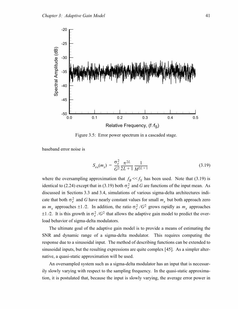
Chapter 3: Adaptive Gain Model 41
baseband error noise is
(3.19)
where the oversampling approximation that has been used. Note that (3.19) is
identical to (2.24) except that in (3.19) both and G are functions of the input mean. As
discussed in Sections 3.3 and 3.4, simulations of various sigma-delta architectures indi-
cate that both and G have nearly constant values for small but both approach zero
as approaches ±1 ⁄ 2. In addition, the ratio grows rapidly as approaches
±1 ⁄ 2. It is this growth in that allows the adaptive gain model to predict the over-
load behavior of sigma-delta modulators.
The ultimate goal of the adaptive gain model is to provide a means of estimating the
SNR and dynamic range of a sigma-delta modulator. This requires computing the
response due to a sinusoidal input. The method of describing functions can be extended to
sinusoidal inputs, but the resulting expressions are quite complex [45]. As a simpler alter-
native, a quasi-static approximation will be used.
An oversampled system such as a sigma-delta modulator has an input that is necessar-
ily slowly varying with respect to the sampling frequency. In the quasi-static approxima-
tion, it is postulated that, because the input is slowly varying, the average error power in
0.0 0.1 0.2 0.3 0.4 0.5-50
-45
-40
-35
-30
-25
-20
Relative Frequency, (f ⁄ fS)
Spectral Amplitude (dB)
Figure 3.5: Error power spectrum in a cascaded stage.
See mx( )σe2
G2------
π2L
2L 1+----------------
1
M2L 1+-----------------=
fB << fS
σe2
σe2 mx
mx σe2 G2⁄ mx
σe2 G2⁄

Chapter 3: Adaptive Gain Model 42
the baseband for a sinusoidal input with amplitude , denoted , is equal to the dc
error power averaged over the sinusoid, that is,
(3.20)
No proof is offered for this claim; however, the results generated by using this approxima-
tion agree well with simulations that use the quantization function in (3.1) explicitly.
Since (3.20) is only an approximation, and since explicit integration of is in
practice quite complicated, the integration will be computed using the simple trapezoidal
approximation
(3.21)
where = 1 ⁄ 8 for n = 0 and 4, and = 1 ⁄ 4 for n = 1, 2, and 3.
In addition to quantization noise, real sigma-delta A/D converters have circuit noise
components. Let the circuit noise be modeled as an input referred noise source, and let the
baseband output power due to circuit noise be denoted . If the input referred noise is
white with a variance of , the output power of this noise is
(3.22)
As discussed in Section 3.1, the input transfer function is approximately unity in the
baseband, so is simply
(3.23)
If it is assumed that the quantization noise and the circuit noise are uncorrelated, the
total output noise power is the sum of the quantization noise power and the circuit noise
power. The SNR is the ratio of the output signal power to the total output noise power.
For a sinusoidal input with an amplitude of , the input signal power is . Since the
input transfer function is unity in the baseband, the output signal power is equal to the
input signal power. With the quasi-static approximation, the signal-to-noise ratio includ-
ing the circuit noise and the quantization noise is thus
Ax Sse Ax( )
Sse Ax( ) See Ax 2πtsin( )dt.
0
1
∫=
See mx( )
Sse Ax( ) anSee Ax
πn8------sin
n 0=
4
∑≈
an an
Sxx
σx2
Sxx
σx2
fS------ Hx e j2πf fS⁄–( ) 2df.
fB–
fB
∫=
Hx z( )
Sxx
Sxx
σx2
M------.=
Ax Ax2 2⁄
Chapter 3: Adaptive Gain Model 43
(3.24)
and the task of computing the SNR is reduced to finding expressions for and G as
functions of a dc input.
3.2.3 Linear System Analysis
By using the white noise approximation and the system equations given in (3.12)–(3.16),
the gain G can be derived as a function of and the output mean . Because the quan-
tizer output is by definition ±1 ⁄ 2, the average total output power of the quantizer must be
1 ⁄ 4. The total output power can also be computed from the linear systems equations
(3.12)–(3.16), and the result is
(3.25)
where
(3.26)
(3.27)
is the z-transform of the autocorrelation of . Note that the integrations in (3.26)
and (3.27) differ significantly from the integrations in (3.18) and (3.22); here the integra-
tion bandwidth spans the entire bandwidth of the modulator, not just the baseband.
Given the modulator architecture and the input x, the expressions in (3.26) and (3.27)
can be evaluated, and (3.25) can be used to solve for G as a function of and . As
shown in (3.17), the output mean is approximately equal to the input mean . Thus,
the only unknown in the SNR expression (3.24) that remains is the error variance .
3.3 Quantizer Error Variance
In this section, it is shown that the quantizer error variance can be expressed as a function
of the output mean and the shape of the quantizer input probability density function, and
some properties of the error variance are derived. Unfortunately, a satisfactory means of
deriving an expression for the error variance itself has not been found. Instead, an expres-
sion that has proven useful in approximating the error variance will be given.
SNRAx2
2 Sse Ax( ) Sxx+( )---------------------------------------=
σe2
σe2 my
y2⟨ ⟩ 1
4--- my
2 Stx Ste+ += =
Stx1
2πj-------- Hx z( ) 2Ψxr z( )
dz
z-----
z =1∫°=
Ste
σe2
2πj-------- He z( ) 2dz
z-----
z =1∫° .=
Ψxr z( ) xr
σe2 my
my mx
σe2
Chapter 3: Adaptive Gain Model 44
3.3.1 Statistical Properties of the Error Variance
To study the statistical properties of the error variance, , the following theorem is
needed. Let w be a function of the stationary and ergodic random signal v, such that
, and let the probability density function (PDF) of v be . It can be shown
[5] that w is also a stationary and ergodic random signal, and that the time average of w is
given by
(3.28)
To simplify the notation in the analysis that follows, it will be useful to make some
additional definitions. Let the PDF, mean, and variance of the quantizer input u be given
by , , and , respectively. A normalized quantizer input PDF, , can then
be defined such that
(3.29)
This normalized PDF has a mean of zero, a variance of one, and will depend only on the
shape of . Using , the following functions can be defined
(3.30)
(3.31)
With the definitions above, the mean of the quantizer output y is
(3.32)
and the cross-correlation of y and is
(3.33)
σe2
w w v( )= ρV v( )
w⟨ ⟩ wρV v( ) dv.
∞–
∞
∫=
ρU u( ) mu σu2 ρN v( )
ρN v( ) σuρU σuv mu+( ).=
ρU u( ) ρN v( )
Φ0 x( ) ρN v( ) dv
x–
∞
∫ ρN v( ) dv
∞–
x–
∫–=
Φ1 x( ) vρN v( ) dv
x–
∞
∫ vρN v( ) dv
∞–
x–
∫ .–=
my yρU u( ) du
∞–
∞
∫1
2---Φ0
mu
σu
------ = =
ur
yur⟨ ⟩ yuρU u( ) du
∞–
∞
∫ mymu–σu
2------Φ1
mu
σu
------ .= =

Chapter 3: Adaptive Gain Model 45
If the inverse of , denoted , exists, (3.32) can be inverted and the normalized
quantizer input mean, , can be written as
(3.34)
Let the spread factor, , be defined as
(3.35)
Note that the spread factor is a function only of and the shape of the PDF of u; it is
independent of and . Substitution of (3.33)–(3.35) into (3.6) and (3.9) yields a
quantizer gain G of
(3.36)
and an error variance of
(3.37)
Because the average quantizer output power, , is by definition 1 ⁄ 4, the output vari-
ance is simply , and (3.37) reduces to
(3.38)
Thus, the error variance is a function solely of the output mean and the shape of the quan-
tizer input PDF.
3.3.2 The Spread Factor
An important component of the error variance expression in (3.38) is the spread factor
. Unfortunately, a means of deriving an expression for the spread factor has not
been found.
Ardalan and Paulos propose assuming a gaussian distribution for the quantizer input u
[45] because the forward path of a sigma-delta modulator is a lowpass filter. Lowpass fil-
tering of a random variable tends to produce a gaussian random variable under certain
Φ0 x( ) Φ01– x( )
mu σu⁄
mu
σu
------ Φ01– 2my( ).=
χu my( )
χu my( ) Φ1 Φ01– 2my( )( ).=
my
mu σu2
Gχu my( )
2σu
----------------=
σe2 σy
2χu2 my( )
4----------------.–=
y2⟨ ⟩
σy2 1 4⁄ my
2–
σe2 1
4--- 1 4my
2– χu2 my( )–( ).=
χu my( )

Chapter 3: Adaptive Gain Model 46
circumstances [46]. Under the assumption that the quantizer input u is a gaussian random
variable, the functions and are
(3.39)
(3.40)
and the spread factor can be computed from (3.39) and (3.40). While this approx-
imation was claimed to be useful in determining the stability of higher-order modulators,
it proved to be inadequate for the architecture optimization purposes of this work. Instead,
empirical studies were used to determine an adequate approximation for the error variance
as a function of the output mean.
One fact about the spread factor that can be derived is the following. From (3.32), it is
evident that when , . Since , by virtue of being a
probability density, is non-negative and integrates to one over all space, can
only be ±1 if one of the two integrations in (3.30) completely encompasses the non-zero
portion of and the remaining integration only includes portions of equal to
zero. Under these circumstances, is simply the mean of , which is zero,
and
(3.41)
As inferred from (3.36) and (3.38), when the spread factor is zero, the quantizer gain G
and error variance must also be zero, and any function designed to approximate the
error variance must satisfy these conditions.
3.3.3 Error Variance Estimation
From studies of the error variance in various sigma-delta architectures, it was found that
the error variance as a function of the output mean can be closely approximated by
(3.42)
where , , and are architecture dependent parameters that are independent of ,
and , defined below, is a peaking function. The first term in this
Φ0 x( ) Φ1 x( )
Φ0 x( ) erfx
2-------
2
π------- e v2– dv
0
x
2-------
∫= =
Φ1 x( )2
π--- e x2 2⁄–=
χu my( )
my 1 2⁄±= Φ0 mu σu⁄( ) 1±= ρn v( )
Φ0 mu σu⁄( )
ρn v( ) ρn v( )
Φ1 mu σu⁄( ) ρn v( )
χu1
2--±( ) 0.=
σe2
σe2 my( ) 1 4my
2–( ) σeo2 1 4my
2–( ) 4κhmy2 κpP my( )+ +[ ]=
σeo2 κh κp my
P x( ) 1 4my2–( )
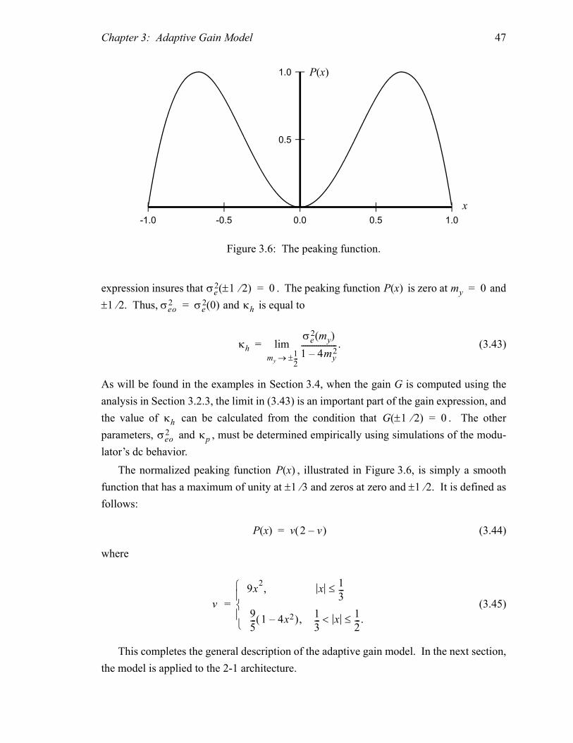
Chapter 3: Adaptive Gain Model 47
expression insures that . The peaking function is zero at and
±1 ⁄ 2. Thus, and is equal to
(3.43)
As will be found in the examples in Section 3.4, when the gain G is computed using the
analysis in Section 3.2.3, the limit in (3.43) is an important part of the gain expression, and
the value of can be calculated from the condition that . The other
parameters, and , must be determined empirically using simulations of the modu-
lator’s dc behavior.
The normalized peaking function , illustrated in Figure 3.6, is simply a smooth
function that has a maximum of unity at ±1 ⁄ 3 and zeros at zero and ±1 ⁄ 2. It is defined as
follows:
(3.44)
where
(3.45)
This completes the general description of the adaptive gain model. In the next section,
the model is applied to the 2-1 architecture.
σe2 1 2⁄±( ) 0= P x( ) my 0=
σeo2 σe
2 0( )= κh
κh
σe2 my( )
1 4my2–
------------------- .
my1
2---±→
lim=
κh G 1 2⁄±( ) 0=
σeo2 κp
P x( )
-1.0 -0.5 0.0 0.5 1.0
0.5
1.0 P(x)
x
Figure 3.6: The peaking function.
P x( ) v 2 v–( )=
v
9x2, x
1
3---≤
9
5--- 1 4x2–( ), 1
3--- x
1
2---.≤<
=

Chapter 3: Adaptive Gain Model 48
3.4 Modeling the 2-1 Architecture
The block diagram of the 2-1 architecture shown earlier in Chapter 2 is repeated here as
Figure 3.7. The standard quantizers and D/A converters from Chapter 2 have been
replaced by the quantization function , and the integration function is again the
delaying integrator defined in (2.18). Heretofore, the adaptive gain model has been
described in terms of a single-stage architecture. The extension to cascaded architectures
is straightforward; the adaptive gain model is applied individually to each stage, and then
the overall baseband performance is computed using the linearized models of each stage.
In the following analysis, a numerical subscript refers to the stage in the 2-1 cascade.
Application of describing functions to the first stage yields a first stage output mean
equal to and a first stage random output that has a z-transform of
(3.46)
where
(3.47)
-
+
Σ
y
-
+
Σ I(z)
-
+
Σ I(z)
+
-Σ
λ
β
H1(z)
H2(z)
+
y1
y2
x2
-
+
Σ I(z)x
b
Figure 3.7: 2-1 Architecture.
Q(u1)
Q(u2)
u1
u2
Q u( ) I z( )
mx
Yr1 z( ) Hx1 z( )Xr z( ) He1 z( )E1 z( )+=
Hx1 z( )G1z
2–
G1 z 2– bz 1– 1 z 1––( )+( ) 1 z 1––( )2+----------------------------------------------------------------------------------------=

Chapter 3: Adaptive Gain Model 49
(3.48)
The dc bias and random inputs to the second stage are then
(3.49)
(3.50)
where
(3.51)
(3.52)
A similar application of describing functions to the second stage yields a second-stage
output mean equal to and a random portion of the second stage output of
(3.53)
where
(3.54)
(3.55)
The dc bias and random outputs of the modulator as a whole are then
(3.56)
(3.57)
where and are chosen to cancel the baseband quantizer error from the first
stage.
The remainder of this section is organized into four subsections as follows. In
Section 3.4.1, expressions for the baseband output and the SNR of the 2-1 architecture are
given. In Sections 3.4.2 and 3.4.3, the adaptive gain model is applied to the first and sec-
He1 z( )1 z 1––( )2
G1 z 2– bz 1– 1 z 1––( )+( ) 1 z 1––( )2+----------------------------------------------------------------------------------------.=
mx2 β λmy1 mu1–( ) β λ 1
K1
------– mx= =
Xr2 z( ) β λYr1 z( ) Ur1 z( )–( ) Hxc z( )Xr z( ) Hec z( )E1 z( )+= =
Hxc z( ) β λ 1
G1
------– Hx1 z( )=
Hec z( ) β λ 1
G1
------– He1 z( )
1
G1
------+ .=
mx2
Yr2 z( ) Hx2 z( )Xr2 z( ) He2 z( )E2 z( )+=
Hx2 z( )G2z
1–
G2z1– 1 z 1––( )+
------------------------------------------=
He2 z( )1 z 1––( )
G2z1– 1 z 1––( )+
------------------------------------------ .=
my H1 1( )mx H2 1( )mx2–=
Yr z( ) H1 z( )Yr1 z( ) H2 z( )Yr2 z( )–=
H1 z( ) H2 z( )
Chapter 3: Adaptive Gain Model 50
ond stages of the modulator, resulting in expressions for the quantizer error variance and
gain for each stage. The parameters for the 2-1 architecture that represent the best design
compromise are then found in Section 3.4.4.
3.4.1 Baseband
It will be found that the digital filters that cancel most of the first-stage quantizer error in
the baseband are
(3.58)
(3.59)
where
(3.60)
As in Chapter 2, is the digital estimate of β, and represents the matching error.
In the baseband, . Neglecting higher order terms and delays, the mean of the
modulator output is equal to and the z-transform of the random portion of modulator’s
baseband output is
(3.61)
As discussed in Section 2.5.2, matching errors in the 2-1 architecture cause a second-order
noise shaped portion of the first-stage quantizer error to leak through to the output. How-
ever, even with perfect matching, for all of the first-stage error to be canceled it is neces-
sary that a be chosen to cancel the third-order shaped component of the first-stage error
appearing in (3.61). Unfortunately, since is a function of the input mean, no single
value of a can cancel this error term for all inputs. So that the best error cancelation is
achieved for low input levels, a is chosen to be
(3.62)
where . For this value for a the baseband modulator output, neglecting
H1 z( ) z 1– 1 a 1 z 1––( )–( )=
H2 z( )1
β--- 1 z 1––( )2=
β β 1 δβ+( ).=
β δβ
z 1≈
mx
Yr z( ) Xr z( ) a 1 b–1
G2
------+ + 1 z1–( )3 δβ 1 z 1––( )2+
E1 z( )
G1
------------+≈
1
β--- 1 z 1––( )3
E2 z( )
G2
------------ .–
G2
a b 1–1
G20
---------–=
G20 G2 mx= 0( )=

Chapter 3: Adaptive Gain Model 51
matching errors, is
(3.63)
Note that under the unity gain approximation in Chapter 2 it was assumed that
= = 1. With this assumption, b = 2, and a = 0, the digital filter functions (3.58)
and (3.59) are identical to (2.45) and (2.46), with the exception of the high order term in
(2.45). From the analysis in this chapter it can be inferred that that higher order term is
superfluous in as much as it cancels a term whose magnitude is smaller than the modeling
error of the unity gain approximation.
Another important aspect of (3.63) is the following. As the input levels increase, the
effective second-stage gain will change, and some of the first-stage error will leak
through to the output. From a total noise perspective, this effect is usually negligible
because both errors are third-order shaped. However, the first-stage error can contain
tones, and as indicated in Figure 2.22, these tones can leak through to the output.
Substitution of each error term from (3.63) into (3.19) yields an error noise in the base-
band of
(3.64)
With this expression and the quasi-static approximation, the SNR can be computed using
(3.24), given expressions for , , , and as functions of the input mean.
These expressions are given below.
3.4.2 First Stage
Substitution of (3.48) into (3.27) results in an average total output error power in the
first stage of
(3.65)
If it is assumed that the input-referred circuit noise variance is much less than the
quantizer error variance , the average total noise power due to can be neglected.
By substituting (3.65) into (3.25), the gain can be written as
(3.66)
Yr z( ) Xr z( )≈ 1
G2
------1
G20
---------– 1 z 1––( )3
E1 z( )
G1
------------1
β--- 1 z 1––( )3
E2 z( )
G2
------------.–+
G20 G2
G2
See mx( )1
G2
------1
G20
---------– 2 σe1
2
G12
--------σe22
β2G22
-------------+π6
7M7----------.=
σe12 G1 σe2
2 G2
Ste12 2b 1–( )
b 1–( ) 4 G1 2b 1–( )–( )---------------------------------------------------------- σe1
2 .=
σx2
σe12 xr
G1
G1
4
2b 1–---------------
8σe12
b 1–( ) 1 4mx2–( )
-----------------------------------------.–=

Chapter 3: Adaptive Gain Model 52
By substituting the approximation expression (3.42) into (3.66) and evaluating the result
in the limit as approaches 1 ⁄ 2, it can be shown that
(3.67)
DC simulations of the first stage for various values of b indicate that reasonable
approximations for and are
(3.68)
(3.69)
It should be noted that there is not thought to be any profound significance to the arctan-
gent function in (3.69); it was simply a readily available function that happened to fit the
data well.
From (3.67)–(3.69), values for and can be computed as a function of the input
mean. Plots of these quantities for b = 2.5 are shown in Figure 3.8, and a plot of
is shown in Figure 3.9. As mentioned previously, an important property of the adaptive
gain model is that both and approach zero as the input mean approaches ±1 ⁄ 2,
mx
κhb 1–
2 2b 1–( )-----------------------.=
σeo12 κp
σeo2 0.0733=
κp 0.0390 0.0423 arctan b 1.741–0.267
---------------------------
.–=
σe12 G1
0.0 0.1 0.2 0.3 0.4 0.50.00
0.02
0.04
0.06
0.08
0.10
0.12
0.14
0.0
0.1
0.2
0.3
0.4
0.5
0.6
0.7
Input Mean (mx)
Quantizer Error Variance (
σe12)
Quantizer Gain (G1)
σe12
G1
Figure 3.8: Quantizer error variance and gain vs. the input mean.
σe12 G1
2⁄
σe12 G1
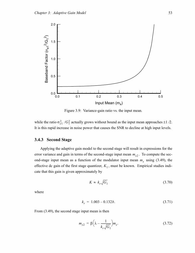
Chapter 3: Adaptive Gain Model 53
while the ratio actually grows without bound as the input mean approaches ±1 ⁄ 2.
It is this rapid increase in noise power that causes the SNR to decline at high input levels.
3.4.3 Second Stage
Applying the adaptive gain model to the second stage will result in expressions for the
error variance and gain in terms of the second-stage input mean . To compute the sec-
ond-stage input mean as a function of the modulator input mean using (3.49), the
effective dc gain of the first stage quantizer, , must be known. Empirical studies indi-
cate that this gain is given approximately by
(3.70)
where
(3.71)
From (3.49), the second stage input mean is then
(3.72)
0.0 0.1 0.2 0.3 0.4 0.50.0
0.5
1.0
1.5
2.0
Input Mean (mx)
Baseband Factor (σ
e12/G
12)
Figure 3.9: Variance-gain ratio vs. the input mean.
σe12 G1
2⁄
mx2
mx
K1
K kr G1≈
kr 1.003 0.132b.–=
mx2 β λ 1
kr G1
----------------– mx.=
Chapter 3: Adaptive Gain Model 54
Though the second stage is only a first order modulator, the computations are signifi-
cantly more complex than those for the first stage because the input to the second stage
has a very strong frequency-shaped random component. Neglecting any random noise
components at the modulator input x, it can be inferred from (3.50) that the random input
to the second stage is a shaped version of the first-stage error. With the white noise
approximation, the average total output power in the second stage due to the second-stage
random input is then
(3.73)
This integral can be evaluated using residue calculus, and the result is
(3.74)
where
(3.75)
(3.76)
(3.77)
(3.78)
(3.79)
The expression for the average total output power in the second stage due to the sec-
ond-stage quantizer error is considerably less complicated than (3.74); substitution of
(3.55) into (3.27) yields
(3.80)
From (3.25), it can be shown that the gain of the second stage, , is a root of the equa-
tion
(3.81)
where
Stx2
σe12
2πj-------- Hec z( )Hx2 z( ) 2 dz
z----- .
z =1∫°=
Stx2βG1
------ 2 G2
2 G2–--------------- 1
c4G2 c5G22+
c1 G1 c2G2 c3G22+ +( )
------------------------------------------------------–
σe12=
c1 b 1–( ) G1 2b 1–( ) 4–( )=
c2 G1 b 2–( )=
c3 1 G1 b 1–( )–=
c4 4 1 λG1–( )2=
c5 2 2b 3–( ) 1 λG1–( )2 2c1 1 λG1–( ).+=
Ste22
2 G2–--------------- σe2
2= .
G2
0 d0 d1G2 d2G22 d3G2
3+ + +=
Chapter 3: Adaptive Gain Model 55
(3.82)
(3.83)
(3.84)
(3.85)
(3.86)
(3.87)
The roots of (3.81) can be computed analytically using the general solution of the
cubic equation [47]. While the roots to (3.81) are quite complicated, one simple fact is
readily derived, namely that for to be zero at = ±1 ⁄ 2, the constant must be
(3.88)
DC simulations of the second stage for various values of b, β, and λ indicate that rea-
sonable approximations for and are
(3.89)
(3.90)
3.4.4 Results
At this point the adaptive gain model for the 2-1 architecture is completely specified.
A comparison between the values calculated using the adaptive gain model and simulated
using the quantization function explicitly for two typical sets of modulator parame-
ters is shown in Figure 3.10. The oversampling ratio is 128. The simulation data points
are shown with circles and diamonds; the smooth lines are computed using the adaptive
gain model. The full scale, or 0 dB, input is defined to be a sinusoid whose amplitude is
equal to the magnitude of the quantizer output level, which in this case is 1 ⁄ 2. For the
examples in Figure 3.10, the model and simulation results agree to within 1 dB, and both
the low- and high-level input characteristics appear to be modeled quite well.
d0 2c1G1 1 σe2n2–( )=
d1 c1 2c2 1 σe2n2–( ) G1 1 σe1n
2+( )–[ ]=
d2 2c1c2 1 σe2n2–( ) c1c2– c4 c1c2–( )σe1n
2+=
d3 c1c3– c5 c1c3–( )σe1n2+=
σe1n2 4
βG1
------ 2 σe1
2
1 4mx22–
---------------------=
σe2n2
4σe22
1 4mx22–
--------------------- .=
G2 mx2 κh
κh
1
4---= .
σeo22 κp
σeo22 0.0824=
κp 0.208 0.0865 b– 0.0242 λ.+=
Q u( )

Chapter 3: Adaptive Gain Model 56
An important characteristic evident from Figure 3.10 is that the SNR peaks at an input
level well below full scale and then declines rapidly for input levels above this peak.
Because of this, the definition of the useful signal range or dynamic range given in
Chapter 2 must be modified. Let the input overload level be defined as the highest input
level at which the SNR is no more than 3 dB below its peak value. The dynamic range is
hereafter defined as the ratio of the input overload power to the input power at which the
SNR is one.
Another aspect of sigma-delta performance exemplified in Figure 3.10 is the trade-off
between the input overload level and low-level signal-to-noise ratio. This is further illus-
trated in Figure 3.11. Here the input overload level and the idle channel noise (the quanti-
zation noise with no input signal) are plotted versus the error gain coefficient β. Both the
input overload level and the idle channel noise increase with decreasing β. In the absence
of any circuit noise, the optimum β is simply the value that maximizes the difference
between the input overload level and the idle channel noise; that is, the value that maxi-
mizes the dynamic range.
On the other hand, if circuit noise, modeled as a non-zero random input , is signifi-
cantly larger than the baseband quantization noise, the dynamic range is much more
dependent on the input overload level. This is illustrated in Figure 3.12. The dynamic
range is plotted both for a quantization noise limited architecture and a circuit noise lim-
b = 2.5 β = 0.5 λ = 2.0 b = 2.0 β = 1.0 λ = 1.0
Figure 3.10: Adaptive gain model and simulation comparison.
-20 -15 -10 -5 090
95
100
105
110
115
120
125
Input Amplitude (dB)
Signal-to-Noise Ratio (dB)
uu u
uu
uu
u u
u u uu
u u u
u uuuuu
u
u
u
ll
l l
ll l l
l ll l l
l
l
l
l
l
l
ll
ul
xr

Chapter 3: Adaptive Gain Model 57
0.0 0.2 0.4 0.6 0.8 1.0 1.2 1.4 1.6-126
-124
-122
-120
-118
-116
-114
-112
-110
-3.5
-3.0
-2.5
-2.0
-1.5
-1.0
-0.5
0.0
Error Gain (β)
Idle Channel Noise (dB)
Input Overload Level (dB)
Noise
Overload
Figure 3.11: Noise and overload level trade-off.
0.0 0.2 0.4 0.6 0.8 1.0 1.2 1.4 1.688
90
92
94
96
98
100
102
Error Gain (β)
Dynamic Range (dB)
M = 64, Quantization Limited
M = 128, Circuit Limited
Figure 3.12: Dynamic range vs. error gain.

Chapter 3: Adaptive Gain Model 58
ited architecture. The oversampling ratios and the amount of circuit noise in the circuit
noise limited architecture are chosen so that the maximum dynamic range attainable in the
quantization and circuit limited cases is approximately the same. In the quantization-
limited case, the maximum dynamic range is obtained at approximately β = 0.9. As the
circuit noise is increased, the maximum dynamic range occurs at lower and lower values
of β. In the strongly circuit noise limited case pictured here, the maximum dynamic range
is obtained at approximately β = 0.12. In this work, the sigma-delta modulator circuit is
expected to operate between these two extremes, so a value of β = 0.5 was chosen as the
design value.
The parameters b and λ are chosen in a similar manner. Plots for these values are
shown in Figures 3.13 and 3.14. In the case of the feedback coefficient b, there is a broad
range of values for which the dynamic range is near its maximum. In both the quantiza-
tion noise limited and the circuit noise limited cases, this range is approximately between
2 and 3. To operate in the middle of this range and to use a value that will be easy to
implement, a value of b = 2.5 was chosen. As discussed in Section 2.6, a feedback coeffi-
cient, b, of 2.5 also has advantages in terms of the spectral noise tone performance.
In the absence of circuit noise, there is a definite peak in the dynamic range as a func-
tion of the error mixing coefficient, λ, at approximately λ = 1.3. As the circuit noise is
increased, this peak broadens and occurs at increasing values of λ. In the strongly circuit
1.5 2.0 2.5 3.0 3.5 4.094
95
96
97
98
99
100
Feedback Coefficient (b)
Dynamic Range (dB)
M = 64, Quantization Limited
M = 128, Circuit Limited
Figure 3.13: Dynamic range vs. feedback coefficient.
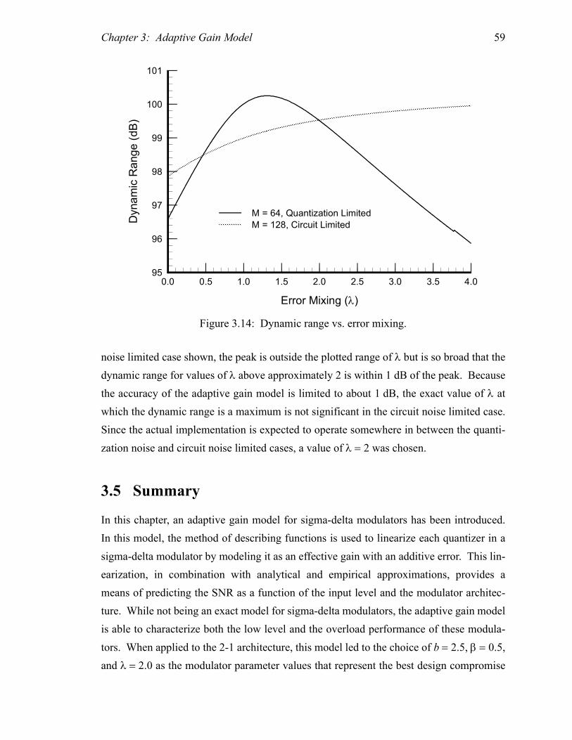
Chapter 3: Adaptive Gain Model 59
noise limited case shown, the peak is outside the plotted range of λ but is so broad that the
dynamic range for values of λ above approximately 2 is within 1 dB of the peak. Because
the accuracy of the adaptive gain model is limited to about 1 dB, the exact value of λ at
which the dynamic range is a maximum is not significant in the circuit noise limited case.
Since the actual implementation is expected to operate somewhere in between the quanti-
zation noise and circuit noise limited cases, a value of λ = 2 was chosen.
3.5 Summary
In this chapter, an adaptive gain model for sigma-delta modulators has been introduced.
In this model, the method of describing functions is used to linearize each quantizer in a
sigma-delta modulator by modeling it as an effective gain with an additive error. This lin-
earization, in combination with analytical and empirical approximations, provides a
means of predicting the SNR as a function of the input level and the modulator architec-
ture. While not being an exact model for sigma-delta modulators, the adaptive gain model
is able to characterize both the low level and the overload performance of these modula-
tors. When applied to the 2-1 architecture, this model led to the choice of b = 2.5, β = 0.5,
and λ = 2.0 as the modulator parameter values that represent the best design compromise
0.0 0.5 1.0 1.5 2.0 2.5 3.0 3.5 4.095
96
97
98
99
100
101
Error Mixing (λ)
Dynamic Range (dB)
M = 64, Quantization Limited
M = 128, Circuit Limited
Figure 3.14: Dynamic range vs. error mixing.

Chapter 3: Adaptive Gain Model 60
in a high-resolution audio application. The remainder of this work is devoted to the imple-
mentation of this architecture.
60
Chapter
4 Modulator Design
Transferring the block diagram of the 2-1 architecture to a device-level description
involves the design of circuits that implement summing integrators, comparators, and one-
bit D/A converters. Circuit deficiencies such as finite speed, thermal noise, and finite sig-
nal swing ultimately limit the performance of the modulator. In this chapter, these limita-
tions are quantified, and means of overcoming some of them are proposed.
The first section in this chapter introduces the circuit blocks that compose a noise-dif-
ferencing sigma-delta modulator, and these blocks are combined to produce a 2-1 architec-
ture. Because circuit noise is such an important factor in high-resolution modulator
design, Section 4.2 provides an extended overview of the types of circuit noise typically
found in modulator circuits, and means of reducing some of the noise components are dis-
cussed. Building on this noise discussion, the remainder of the chapter addresses design
issues specific to the integrators in noise-differencing sigma-delta modulators. In
Section 4.3, various integrator circuit architectures are compared, and in Section 4.4 two
amplifier topologies that can be used to implement the integrators are contrasted. In
Section 4.5, models for three types of integrator circuit limitations are proposed and used
to establish the design specifications for the integrator circuit elements. Finally, the analy-
ses in this chapter are combined in Section 4.6, leading to the specification of a high-reso-
lution sigma-delta modulator circuit topology.
4.1 Modulator Building Blocks
Typically, the most important building blocks in the analog portion of a noise-differ-
encing sigma-delta modulator are the summing integrators. These integrator circuits are
normally designed to implement the block diagram shown in Figure 4.1. The output of

Chapter 4: Modulator Design 61
this integrator, w, is a delayed integration of a weighted sum of inputs, . In the time
domain, the output is
(4.1)
where is the sampling period. The output can also be written in the z-transform
domain as
(4.2)
where and are the z-transforms of and w, respectively.
The remaining building blocks in the analog portion of the modulator are comparators
and one-bit D/A converters. The comparator circuits act as a one-bit A/D converters; they
map their inputs to one of two digital output codes. These two digital output codes are
then mapped back into analog levels by the D/A converters. For simplicity, let the two
output codes of the comparators be defined as ±1 ⁄ 2. With this definition, the comparators
can be described by the quantization function defined in (3.1) and the D/A convert-
ers, neglecting D/A errors, can be represented simply by gain blocks.
By combining three summing integrators with two comparators and two one-bit D/A
converters, a 2-1 architecture can be constructed as shown in Figure 4.2. The D/A con-
verters are represented by the gain blocks and . Since ideally the gain at the input
of a comparator is irrelevant, this system produces outputs identical to those in the 2-1
architecture depicted in Figure 3.7, provided that
(4.3)
v1
v2
a1
a2 Σ+
z-1 w
Figure 4.1: Integrator block diagram.
vi
w n 1+( )TS( ) w nTS( ) aivi nTS( )
i∑+=
TS
W z( )z 1–
1 z 1––---------------- aiVi z( )
i∑=
Vi z( ) W z( ) vi
Q x( )
∆1 ∆2
xai1
af1∆1
------------- vi=

Chapter 4: Modulator Design 62
(4.4)
(4.5)
(4.6)
While Figure 4.2 shows the basic form of the implementation of a 2-1 architecture,
real analog circuit blocks do not precisely perform their ideal function. The remainder of
this chapter is devoted to studying the effect of non-idealities in the modulator building
blocks in an effort to determine the circuit topologies that best meet the performance
requirements of the modulator. The primary emphasis in this discussion is on the limita-
tions in modulator performance imposed by the integrators.
ai1
−af1
ai2
−af2
−au3
ai3
−af3
Σ ∫ Σ ∫
Σ ∫
Q(w2)
Q(w3)
∆1
∆2
y1
y2
vi
Integrator #1 Integrator #2
Integrator #3
w1
w2
w3
Figure 4.2: 2-1 architecture implementation.
baf2
af1ai2
--------------=
βaf1ai2au3
af3
----------------------∆1
∆2
------=
λai3
af1ai2au3
----------------------.=
Chapter 4: Modulator Design 63
4.2 Circuit Noise
In high-resolution sigma-delta modulators, the signal-to-noise ratio at low input levels is
often limited by circuit noise rather than quantization noise. There are two types of circuit
noise that dominate in typical sigma-delta modulator implementations: white noise and
flicker, or 1 ⁄ f, noise [48]. White noise is characterized by a power spectral density that is
constant with frequency. 1 ⁄ f noise, as the name indicates, has a power spectral density
that is inversely proportional to frequency. Since these random noise sources are statisti-
cally independent, their power spectra add. The total noise power is usually limited by the
overall bandwidth of the circuit. If this bandwidth is expressed as a one-pole roll-off in
the power spectrum, the total noise spectral density, , can be written
(4.7)
where is the white noise density, K is the 1 ⁄ f noise coefficient, and τ is the time con-
stant of the single-pole band limit. As is traditional in circuit noise expressions, this
power spectrum is single-sided. The lower limit of this single-sided spectrum is defined
arbitrarily to be some , where . Since the power spectrum of a random sequence
is symmetric, the equivalent two-sided noise spectrum, , is simply
(4.8)
When the noise is sampled by a sigma-delta modulator, any noise components appear-
ing at frequencies greater than half the modulator’s sampling frequency will be aliased or
folded into the modulator’s sampling bandwidth. The effect of this aliasing is that the
total noise power in the output signal’s baseband, , is equal to the sum of the noise
found within baseband-width windows centered about multiples of the sampling fre-
quency. Expressed mathematically,
(4.9)
where is the baseband width, is the low frequency limit, and is the sampling fre-
quency. If it is assumed that << << , then the total baseband noise power is
ξ f( )
ξ f( )
ξo
K
f----+
1 2πτf( )2+----------------------------=
ξo
fL fL 0>
ξ2 f( )
ξ2 f( ) 12---ξ f( ).=
SN
SN ξ f mfS–( ) df
fL
fB
∫m ∞–=
∞
∑=
fB fL fS
fL fB fS
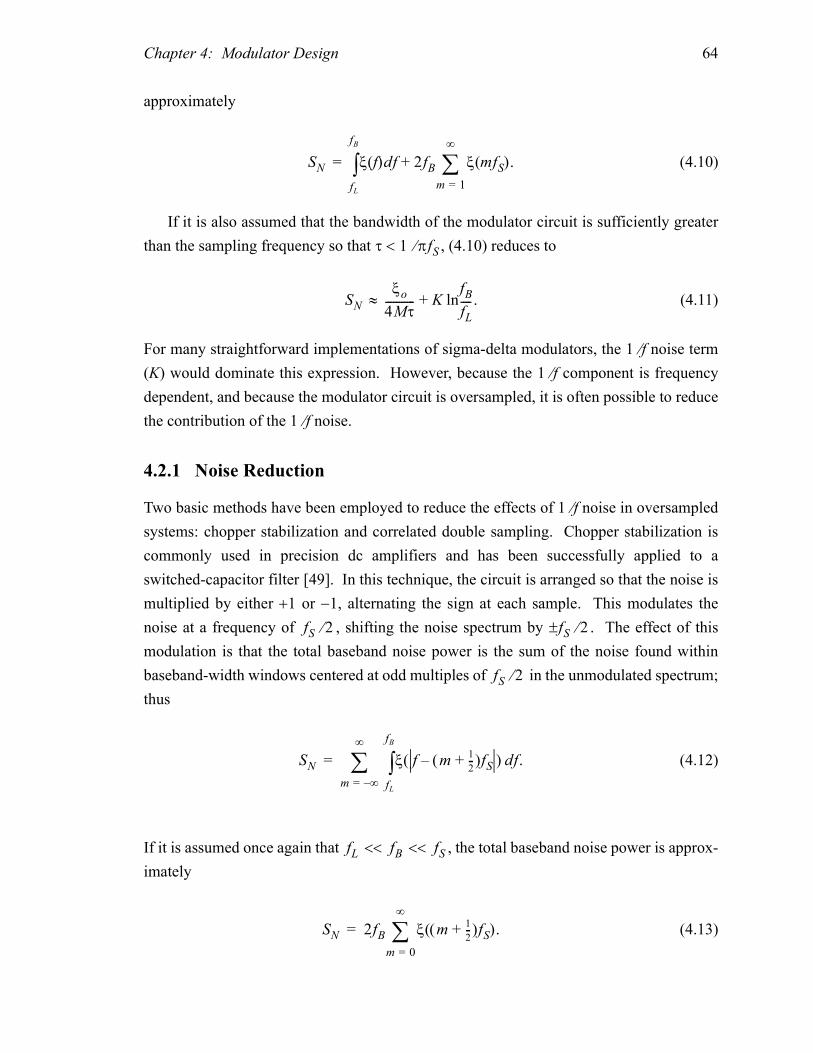
Chapter 4: Modulator Design 64
approximately
(4.10)
If it is also assumed that the bandwidth of the modulator circuit is sufficiently greater
than the sampling frequency so that , (4.10) reduces to
(4.11)
For many straightforward implementations of sigma-delta modulators, the 1 ⁄ f noise term
(K) would dominate this expression. However, because the 1 ⁄ f component is frequency
dependent, and because the modulator circuit is oversampled, it is often possible to reduce
the contribution of the 1 ⁄ f noise.
4.2.1 Noise Reduction
Two basic methods have been employed to reduce the effects of 1 ⁄ f noise in oversampled
systems: chopper stabilization and correlated double sampling. Chopper stabilization is
commonly used in precision dc amplifiers and has been successfully applied to a
switched-capacitor filter [49]. In this technique, the circuit is arranged so that the noise is
multiplied by either +1 or −1, alternating the sign at each sample. This modulates the
noise at a frequency of , shifting the noise spectrum by . The effect of this
modulation is that the total baseband noise power is the sum of the noise found within
baseband-width windows centered at odd multiples of in the unmodulated spectrum;
thus
(4.12)
If it is assumed once again that << << , the total baseband noise power is approx-
imately
(4.13)
SN ξ f( )df
fL
fB
∫ 2fB ξ mfS( )
m 1=
∞
∑ .+=
τ 1 πfS⁄<
SN
ξo
4Mτ----------- K ln
fB
fL----+ .≈
fS 2⁄ fS 2⁄±
fS 2⁄
SN ξ f m1
2--+( )fS–( ) df.
fL
fB
∫m ∞–=
∞
∑=
fL fB fS
SN 2fB ξ m1
2--+( )fS( )
m 0=
∞
∑ .=

Chapter 4: Modulator Design 65
If it is also assumed that the modulator circuit is enough faster than the sampling fre-
quency such that , (4.13) reduces to
(4.14)
In comparison to the unchopped case in (4.11), there is no change in the total white noise
component but the 1 ⁄ f noise has been reduced by a factor on the order of the oversampling
ratio.
An alternative to chopper stabilization is correlated double sampling (CDS). CDS was
first developed for charge-coupled devices [50, 51]. In a CDS system, the noise is mea-
sured in one sampling time period and subtracted in the next sampling period. This pro-
duces a first-order difference that shapes the circuit noise much like a sigma-delta
modulator shapes its quantization noise. The resulting shaped noise spectrum, , is
(4.15)
where is the correlation sampling rate. The total noise in the baseband is found by sub-
stituting (4.15) into (4.9).
Typically, the correlation sampling rate is either or ; that is, the sample delay is
either one clock period or one-half of one clock period. When the correlation sampling
rate is equal to the modulator’s sampling rate, the nulls in the noise shaping occur at mul-
tiples of the sampling frequency, and all of the aliased noise components are greatly
reduced. If it is assumed that << , the total baseband noise power is approximately
(4.16)
This is a substantial improvement over chopper stabilization with respect to both white
and 1 ⁄ f noise reduction.
On the other hand, when the correlation sampling rate is twice the modulator’s sam-
pling rate, peaks in the noise shaping occur at odd multiples of the sampling frequency.
The low frequency components are still reduced, but the aliased components are actually
amplified. The total baseband noise power in this case is approximately
(4.17)
τ 1 πfS⁄<
SN
ξo
4Mτ-----------
4K
M-------+ .≈
ξS f( )
ξS f( ) ξ f( ) 1 e j2πf fC⁄–– 2=
fC
fS 2fS
fB fS
SN
ξoπ2
12M3τ----------------
Kπ2
2M2----------+≈ .
SN
ξo
2Mτ-----------
8K
M-------+ .≈

Chapter 4: Modulator Design 66
Thus, instead of being an improvement over chopper stabilization, both the white and 1 ⁄ f
noise power are a factor of 2 larger. Even so, CDS at twice the sampling rate offers a sub-
stantial reduction in 1 ⁄ f noise compared to the uncorrelated 1 ⁄ f noise in (4.11).
4.2.2 Noise Shaping in the Modulator
In addition to chopper stabilization and CDS techniques, the noise from many components
in a sigma-delta modulator is naturally reduced by the same processes that reduce the
quantization noise. In the modulator depicted in Figure 4.2, each of the circuit blocks con-
tains components that generate noise. All of these noise sources except those in the first
integrator and the first stage D/A converter are attenuated by the noise shaping feedback
of the modulator.
Noise generated in the integrators can be modeled with input-referred noise generators
at the , , and inputs. Let these noise generators be denoted , , and ,
respectively. These noise generators can equivalently be modeled by a single noise gener-
ator at the input , which will be denoted . If delays are neglected, the equivalent
input-referred noise is
(4.18)
The noise generated in the second and third integrators is shaped by the feedback loops of
the modulator. The noise in the second integrator is shaped by a first-order difference, and
the noise in the third integrator is shaped by a second-order difference.
Let the white noise components of the noise sources and be and ,
respectively, and let the 1 ⁄ f noise coefficients of these noise terms be and , respec-
tively. If it is assumed that << , the total input-referred baseband noise power is
approximately
(4.19)
where is the input-referred baseband noise power of the first integrator. In high-reso-
lution applications, the oversampling ratio, M, is usually large enough that both the white
and 1 ⁄ f noise components from the second and third integrators are negligible, and the
first integrator’s noise dominates the circuit noise of the modulator.
Input-referred noise in the comparators is also shaped. In fact, this noise receives the
same shaping and error cancellation as the quantizer error. Since the unshaped quantizer
ai1 ai2 au3 ni1 ni2 nu3
vi ni
ni ni11 z 1––( )ai1
--------------------- ni21 z 1––( )2
ai1ai2
----------------------- nu3.+ +=
ni2 nu3 ξo1 ξo2
K2 K3
fB fS
SN SN1π2
ai1M2
--------------ξo2
12Mτ--------------
K2
2-------+
+≈ π4
ai1ai2M4
----------------------ξo3
20Mτ--------------
K3
4-------+
+
SN1

Chapter 4: Modulator Design 67
error power is quite large, it is relatively easy to design the comparator such that its noise
contribution is negligible. On the other hand, noise in the D/A converters adds directly to
the input. Fortunately, the one-bit D/A converters can be implemented simply as a switch
between two reference levels, and many applications are insensitive to the accuracy of
these reference levels. Nonetheless, care must be taken in the design of the reference sup-
plies to insure that their noise does not impact the modulator.
4.2.3 Noise Sources
To quantify circuit noise in the modulator, the white noise density and the 1 ⁄ f noise
coefficient K must be computed. For compatibility with existing CMOS processes, the
only components used in the circuits in this work are MOS transistors and capacitors.
Since capacitors have no inherent noise components, the circuit noise is generated only by
the MOS devices. In this section, the origins of MOS noise sources are discussed and
their magnitudes are quantified.
In an MOS transistor, white noise is thermally generated by the resistance in the con-
ducting channel. This is comparable to a conventional resistor, wherein white noise is
generated thermally by the random motion of electrons. In a resistor, the noise produced
by this random motion can be modeled as a parallel current source whose noise spectrum
is flat with a spectral density of
(4.20)
where k is Boltzmann’s constant ( J ⁄ K), T is the absolute temperature, and R
is the resistance [52]. Alternatively, this thermal noise can be represented by a series volt-
age source whose spectral density is
(4.21)
Although thermal noise in the conductive channel of an MOS transistor is caused by a
mechanism similar to that in a conventional resistor, the situation is complicated by the
position dependance of the resistance through the channel when there is a non-zero drain
voltage. Ideally, the noise in the channel can be represented by an additional drain current
component that has a spectral density of
(4.22)
where is the transconductance of the MOS device in saturation and γ varies from a
value of 1 at zero drain-to-source voltage to a value of approximately 2 ⁄ 3 in saturation
ξo
ξo 4kT1
R---=
1.380623–×10
ξo 4kTR.=
in
ξo 4kTγgm=
gm
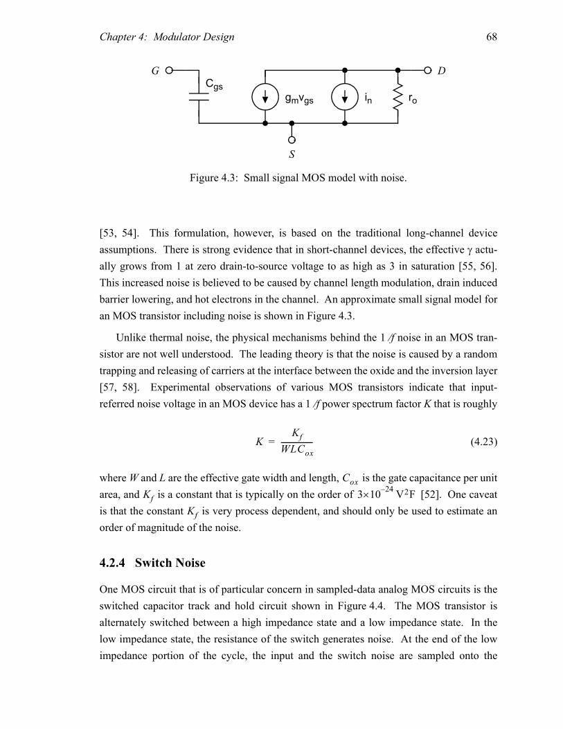
Chapter 4: Modulator Design 68
[53, 54]. This formulation, however, is based on the traditional long-channel device
assumptions. There is strong evidence that in short-channel devices, the effective γ actu-
ally grows from 1 at zero drain-to-source voltage to as high as 3 in saturation [55, 56].
This increased noise is believed to be caused by channel length modulation, drain induced
barrier lowering, and hot electrons in the channel. An approximate small signal model for
an MOS transistor including noise is shown in Figure 4.3.
Unlike thermal noise, the physical mechanisms behind the 1 ⁄ f noise in an MOS tran-
sistor are not well understood. The leading theory is that the noise is caused by a random
trapping and releasing of carriers at the interface between the oxide and the inversion layer
[57, 58]. Experimental observations of various MOS transistors indicate that input-
referred noise voltage in an MOS device has a 1 ⁄ f power spectrum factor K that is roughly
(4.23)
where W and L are the effective gate width and length, is the gate capacitance per unit
area, and is a constant that is typically on the order of [52]. One caveat
is that the constant is very process dependent, and should only be used to estimate an
order of magnitude of the noise.
4.2.4 Switch Noise
One MOS circuit that is of particular concern in sampled-data analog MOS circuits is the
switched capacitor track and hold circuit shown in Figure 4.4. The MOS transistor is
alternately switched between a high impedance state and a low impedance state. In the
low impedance state, the resistance of the switch generates noise. At the end of the low
impedance portion of the cycle, the input and the switch noise are sampled onto the
G
S
D
Cgs
gmvgs in ro
Figure 4.3: Small signal MOS model with noise.
KKf
WLCox
-----------------=
Cox
Kf 324–×10 V2F
Kf

Chapter 4: Modulator Design 69
capacitor. The spectral density of the noise voltage sampled across the capacitor has a
white noise coefficient that is
(4.24)
where is the transconductance that the switch transistor would have if it were in satura-
tion, which, according to the simple square law model of MOS devices, is equal to the
channel conductance with zero drain-to-source voltage. The drain-to-source voltage of
the transistor has been assumed to be close to zero so that γ for the transistor is approxi-
mately 1. Since the bandlimiting time constant of the circuit is τ = C ⁄ , the total sam-
pled noise power in the baseband, according to (4.11), is
(4.25)
Thus, the switch noise is independent of the switch resistance and inversely proportional
to the capacitance and the oversampling ratio.
The analysis leading to (4.25) was simple largely because the calculation of the noise
bandwidth was simple. In general, computing the noise bandwidth in a switched capacitor
circuit is much more complex [59]. To simplify the analysis in the sections that follow, the
switch noise will simply be estimated by assuming one kT ⁄ MC noise contribution from
each independent switch path.
In the above discussion, no mention was made of the switch’s 1 ⁄ f noise. Traditionally,
the 1 ⁄ f noise of the switch is neglected, and empirical evidence supports this omission.
An intuitive explanation for this is that the MOS devices are constantly being turned off,
resetting the oxide trap states. Because of this, the low frequency trapping that causes the
flicker noise never has an opportunity to occur.
vin vout
φ
gmC
Figure 4.4: Switched capacitor noise subcircuit.
ξo 4kT1
gm
------=
gm
gm
SN
kT
MC---------= .
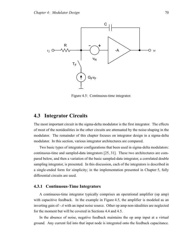
Chapter 4: Modulator Design 70
4.3 Integrator Circuits
The most important circuit in the sigma-delta modulator is the first integrator. The effects
of most of the nonidealities in the other circuits are attenuated by the noise-shaping in the
modulator. The remainder of this chapter focuses on integrator design in a sigma-delta
modulator. In this section, various integrator architectures are compared.
Two basic types of integrator configurations that been used in sigma-delta modulators:
continuous-time and sampled-data integrators [25, 31]. These two architectures are com-
pared below, and then a variation of the basic sampled-data integrator, a correlated double
sampling integrator, is presented. In this discussion, each of the integrators is described in
a single-ended form for simplicity; in the implementation presented in Chapter 5, fully
differential circuits are used.
4.3.1 Continuous-Time Integrators
A continuous-time integrator typically comprises an operational amplifier (op amp)
with capacitive feedback. In the example in Figure 4.5, the amplifier is modeled as an
inverting gain of −A with an input noise source. Other op amp non-idealities are neglected
for the moment but will be covered in Sections 4.4 and 4.5.
In the absence of noise, negative feedback maintains the op amp input at a virtual
ground. Any current fed into that input node is integrated onto the feedback capacitance.
Figure 4.5: Continuous-time integrator.
-A
C
w
vN
+-
vI
R
TF
GFvF
Chapter 4: Modulator Design 71
In practice, the input current is generated either by an input voltage source connected
through a resistor or by a clocked current source; both are illustrated in Figure 4.5. The
resistor injects a current of into the op amp input node. The clocked current source
is typically used to provide the feedback from the one-bit D/A converter in the modulator
loop [25]; a current of is injected into the integrator for a time , where
. The current injection period is typically half of the sampling period.
If it is assumed that the integrator output is ultimately sampled with a sampling period
and that the integrator inputs are approximately constant over the sampling period, the
integrator output at a time for the continuous-time integrator is approximately
(4.26)
A significant difference between this expression and (4.1) is the presence of a leakage
term. In the absence of any inputs, that is if = = = 0, the integrator output will
not hold the value from the previous clock cycle indefinitely. Instead, the output will
decay toward zero, losing a fraction, , of its value at each clock cycle. As will be
discussed in Section 4.5.2, this leakage limits the ability of the modulator to shape the
noise and thus increases the baseband noise due to quantization.
Because the noise generated in the continuous-time integrator by the resistor R and the
amplifier is not sampled until after it is integrated, any input-referred noise components
that are aliased into the baseband by that sampling are also spectrally shaped by the feed-
back loop of the modulator. Thus, the only significant noise components in this integrator
are those in the baseband, and the input-referred baseband noise power is
(4.27)
where is the amplifier’s input-referred white noise spectral density, and is the
amplifier’s 1 ⁄ f noise coefficient. Because of the absence of noise aliasing, the input-
referred white noise of this integrator is usually much lower than that in a comparable
sampled-data integrator. Unfortunately, the techniques that can be used in a sampled-data
integrator to reduce the 1 ⁄ f noise, such as chopper stabilization or CDS, require sampling,
or switching, within the integrator and cannot be used in a continuous-time integrator.
An additional, and perhaps most troublesome, source of noise in the continuous-time
integrator is clock jitter in the switched-current feedback. Clock jitter manifests itself as a
vI R⁄
GFvF TF
vF ∆1 2⁄±= TF
TS
n 1+( )TS
w n 1+( )TS( ) 1TS
ARC------------–
w nTS( )TS
RC--------– vI nTS( ) vN nTS( )+( )=
GFTF
C-------------vF nTS( ).–
vI vN vF
TS ARC⁄
SN 4kT R ξoa+( )fB Ka lnfB
fL----
+=
ξoa Ka
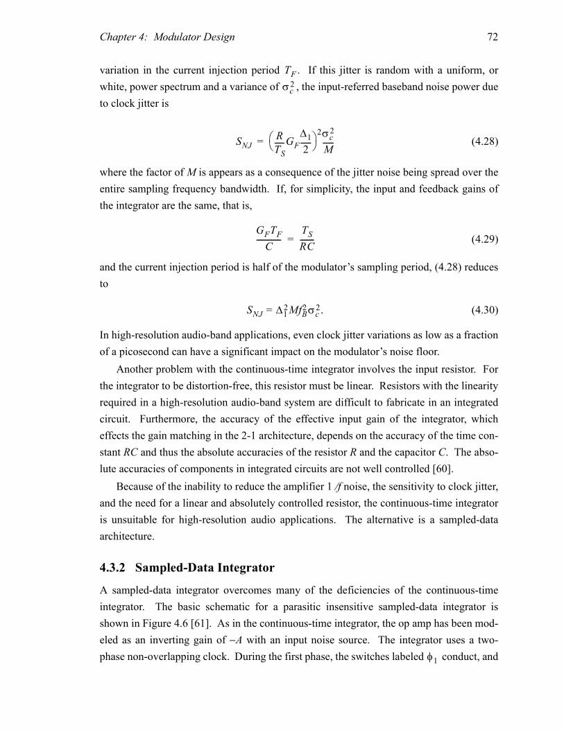
Chapter 4: Modulator Design 72
variation in the current injection period . If this jitter is random with a uniform, or
white, power spectrum and a variance of , the input-referred baseband noise power due
to clock jitter is
(4.28)
where the factor of M is appears as a consequence of the jitter noise being spread over the
entire sampling frequency bandwidth. If, for simplicity, the input and feedback gains of
the integrator are the same, that is,
(4.29)
and the current injection period is half of the modulator’s sampling period, (4.28) reduces
to
(4.30)
In high-resolution audio-band applications, even clock jitter variations as low as a fraction
of a picosecond can have a significant impact on the modulator’s noise floor.
Another problem with the continuous-time integrator involves the input resistor. For
the integrator to be distortion-free, this resistor must be linear. Resistors with the linearity
required in a high-resolution audio-band system are difficult to fabricate in an integrated
circuit. Furthermore, the accuracy of the effective input gain of the integrator, which
effects the gain matching in the 2-1 architecture, depends on the accuracy of the time con-
stant RC and thus the absolute accuracies of the resistor R and the capacitor C. The abso-
lute accuracies of components in integrated circuits are not well controlled [60].
Because of the inability to reduce the amplifier 1 ⁄ f noise, the sensitivity to clock jitter,
and the need for a linear and absolutely controlled resistor, the continuous-time integrator
is unsuitable for high-resolution audio applications. The alternative is a sampled-data
architecture.
4.3.2 Sampled-Data Integrator
A sampled-data integrator overcomes many of the deficiencies of the continuous-time
integrator. The basic schematic for a parasitic insensitive sampled-data integrator is
shown in Figure 4.6 [61]. As in the continuous-time integrator, the op amp has been mod-
eled as an inverting gain of −A with an input noise source. The integrator uses a two-
phase non-overlapping clock. During the first phase, the switches labeled conduct, and
TF
σc2
SNJR
TS
-----GF
∆1
2------
2σc2
M------=
GFTF
C-------------
TS
RC--------=
SNJ ∆12MfB
2σc2= .
φ1
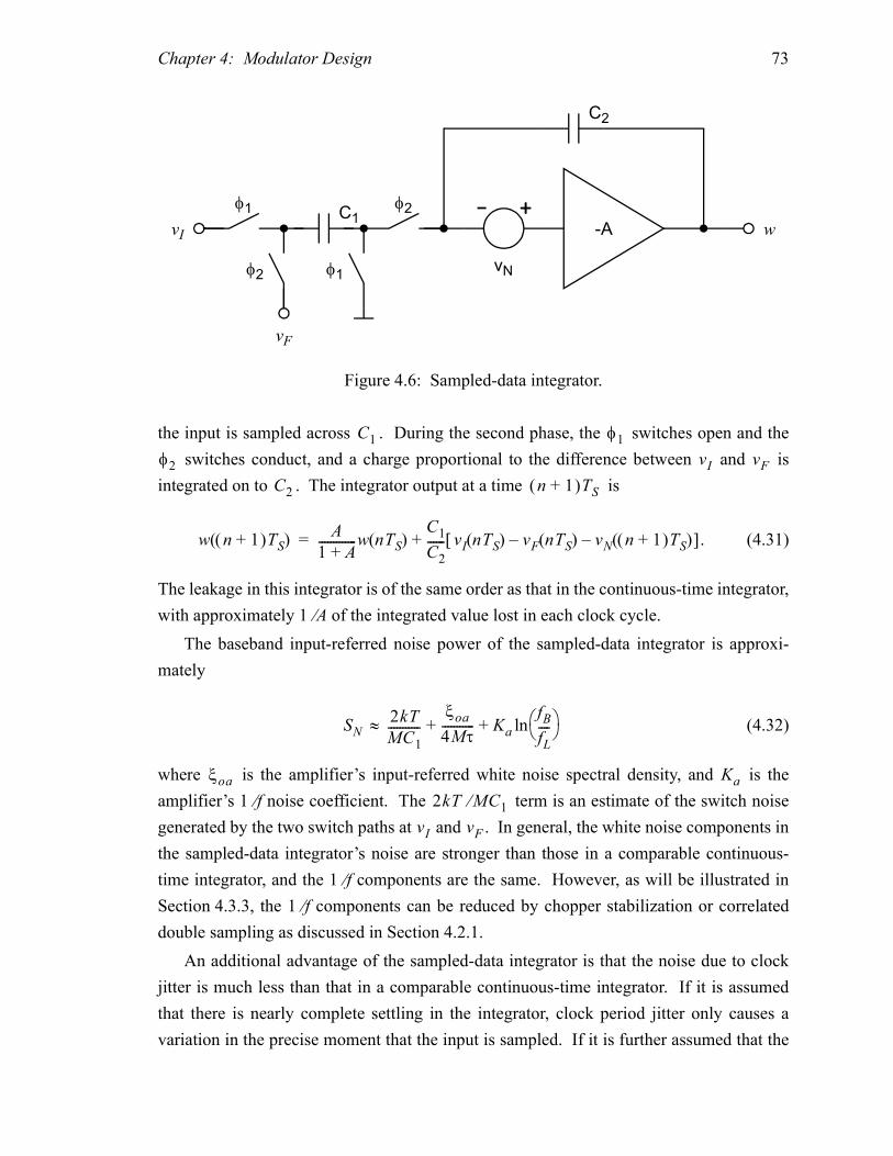
Chapter 4: Modulator Design 73
the input is sampled across . During the second phase, the switches open and the
switches conduct, and a charge proportional to the difference between and is
integrated on to . The integrator output at a time is
(4.31)
The leakage in this integrator is of the same order as that in the continuous-time integrator,
with approximately 1 ⁄ A of the integrated value lost in each clock cycle.
The baseband input-referred noise power of the sampled-data integrator is approxi-
mately
(4.32)
where is the amplifier’s input-referred white noise spectral density, and is the
amplifier’s 1 ⁄ f noise coefficient. The term is an estimate of the switch noise
generated by the two switch paths at and . In general, the white noise components in
the sampled-data integrator’s noise are stronger than those in a comparable continuous-
time integrator, and the 1 ⁄ f components are the same. However, as will be illustrated in
Section 4.3.3, the 1 ⁄ f components can be reduced by chopper stabilization or correlated
double sampling as discussed in Section 4.2.1.
An additional advantage of the sampled-data integrator is that the noise due to clock
jitter is much less than that in a comparable continuous-time integrator. If it is assumed
that there is nearly complete settling in the integrator, clock period jitter only causes a
variation in the precise moment that the input is sampled. If it is further assumed that the
Figure 4.6: Sampled-data integrator.
-A
C2
w
vN
+-
vI
φ1
vF
φ2
C1
φ1
φ2
C1 φ1
φ2 vI vF
C2 n 1+( )TS
w n 1+( )TS( )A
1 A+-------------w nTS( )
C1
C2
------ vI nTS( ) vF nTS( )– vN n 1+( )TS( )–[ ]+ .=
SN2kT
MC1
-----------ξoa
4Mτ----------- Ka ln
fB
fL----
+ +≈
ξoa Ka
2kT MC1⁄
vI vF
Chapter 4: Modulator Design 74
jitter is random with a uniform, or white, power spectrum, the input-referred noise caused
by this jitter has been shown to be bounded by [31]
(4.33)
Therefore, the jitter noise in a sampled-data integrator is a factor of less than that
in a continuous-time integrator.
In addition to the improvement in sensitivity to clock jitter, the linearity of the sam-
pled-data integrator is not limited by a resistive component. The integrator gains are set
by capacitance ratios, rather than absolute capacitance values, and ratios of components
are much better controlled in integrated circuits than are absolute component values [60].
Because of their improved jitter sensitivity, linearity, and capability to reduce the
effect of the amplifier’s 1 ⁄ f noise, sampled-data integrators were used to implement the
2-1 architecture in this work. The thermal noise was controlled by using sufficiently large
capacitors, and the 1 ⁄ f noise was attenuated by incorporating correlated double sampling
into the integrator.
4.3.3 Correlated Double Sampling Integrator
The basic schematic of a correlated double sampling (CDS) integrator is shown in
Figure 4.7 [62]. As with the simple sampled-data integrator in Figure 4.6, a two-phase
non-overlapping clock is used. During the first phase the switches labeled close. The
input is sampled across , and the amplifier noise is sampled onto . During the
second phase, the switches open and the switches conduct. A charge proportional
SNJ
∆12
8------
2πfB( )2σc2
M------------------------- .≤
4M2 π2⁄
-A
C2
w
vN
+-
vI
φ1
vF
φ2
C1
φ1
C3
φ2 φ1
Figure 4.7: Correlated double sampling integrator.
φ1
vI C1 C3
φ1 φ2

Chapter 4: Modulator Design 75
to the difference between and is integrated on to , and the low frequency 1 ⁄ f
noise of the amplifier is canceled by the voltage stored on . The offset capacitor is
normally designed to be much larger than the amplifier’s input capacitance; if this is so,
the integrator output is
(4.34)
Not only does the CDS integrator shape the amplifier noise by a first-order difference, but
the integrator leak is now 1 ⁄ compared to 1 ⁄ A for the simple sampled-data integrator.
In a chopper stabilized version of the sampled-data integrator [49], the integrator leak is
still roughly 1 ⁄ A. Thus, while the correlation sampling rate of means that the ampli-
fier noise in the CDS integrator will be twice that of a chopper-stabilized integrator, the
leakage is greatly reduced. For this reason, the CDS integrator was used for the first inte-
grator in this work. In other implementations in which integrator leak was not an issue, a
chopper stabilized integrator might be preferable.
From the derivation in Section 4.2.1 it can be deduced that the baseband input-referred
noise power of the CDS integrator is approximately
(4.35)
where is the amplifier’s input-referred white noise spectral density, is the ampli-
fier’s 1 ⁄ f noise coefficient and the term is an estimate of the switch noise gen-
erated by the two switch paths at and .
4.4 Amplifier Design
In capacitive load applications, such as the CDS integrator in Figure 4.7, several amplifier
architectures have been used successfully. The more common approaches include single-
stage class A amplifiers, two-stage class A amplifiers, and single-stage class AB amplifi-
ers [65]. Among these types of amplifiers, the single-stage class A amplifier has the wid-
est bandwidth and the single-stage class AB has the best slew rate.
This section focuses on single-stage and two-stage class A amplifiers. While class AB
amplifiers can have a slew rate that is superior to class A amplifiers [63], they were not
considered for this work primarily because they have the highest input-referred noise of
vI vF C2
C3 C3
w n 1+( )TS( ) 11
A2------–
w nTS( )=
C1
C2
------ vI nTS( ) vF nTS( )– vN n 1+( )TS( ) vN n1
2--+( )TS( )+–[ ].+
A2
2fS
SN2kT
MC1
-----------ξoa
2Mτ-----------
8Ka
M---------+ +≈
ξoa Ka
2kT MC1⁄
vI vF

Chapter 4: Modulator Design 76
the three types of amplifiers mentioned above. In addition, they have the greatest circuit
complexity and the possibility of crossover distortion. Recently published work [64] pro-
poses an alternative AB biasing scheme that reduces the input-referred noise, and this
arrangement should be considered in future designs.
4.4.1 Single-Stage Amplifier
A simplified, single-ended, folded-cascode version of the single-stage amplifier [66] is
shown in Figure 4.8. The bias circuitry is not shown in this figure, and it is assumed that
all transistors are biased in the saturation region. The amplifier is shown enclosed in a
capacitive feedback loop to approximate its environment within the integrator. The small-
signal open loop gain of the amplifier is approximately
vI w
bias
bias
bias
bias
M1
M2
M3
M4
M5
C1
C2
ID ID
Figure 4.8: Single-stage folded-cascode amplifier.
Chapter 4: Modulator Design 77
(4.36)
where , , and are the transconductance, output conductance, and output resis-
tance, respectively, of the transistor Mi.
By replacing each of the transistors in the amplifier with the small signal model of
Figure 4.3, the white noise coefficient of the input-referred noise voltage is found to be
(4.37)
This noise is approximately bandlimited by a single pole whose time constant, τ, is
(4.38)
This time constant is also approximately the settling time constant of the amplifier. The
amplifier also has a non-dominant pole at the frequency , where
(4.39)
and is the node capacitance at the source of M3. This non-dominant pole is near the
unity gain frequency of M3, which is close to the upper limit of the speed of the technol-
ogy.
Like all op amps, the amplifier of Figure 4.8 has a maximum rate at which the output
voltage can change. This rate, called the slew rate, is denoted herein as ζ and is approxi-
mately
(4.40)
where is the quiescent drain current in the transistors M1 and M3–M5. A useful mea-
sure of the amplifier’s noise and slew performance is the product of the noise bandwidth
time constant and the slew rate, hereafter called the noise-slew product. For the single-
stage amplifier, the noise-slew product is
(4.41)
Agm1
go1 go2+
gm3ro3----------------------
go5
gm4ro4----------------+
---------------------------------------------=
gmi goi roi
ξoa 4γkT 1
gm1
-------- 1gm2
gm1
--------gm5
gm1
--------+ + .=
τC1
gm1
--------.=
ωnd
ωnd
gm3
Cx
--------=
Cx
ζID
C2
------=
ID
τζC1
C2
------ID
gm1
--------C1
2C2
--------- VGS1 VT1–( )= =

Chapter 4: Modulator Design 78
where is the quiescent gate-to-source voltage of M1, is the threshold of M1,
and a simple square law model of the MOS devices has been used. Note that the noise-
slew product is independent of all transistor sizes. In the next section, the noise-slew
product is used to compare this amplifier to the two-stage amplifier.
4.4.2 Two-Stage Amplifier
A single-ended version of a two-stage amplifier that uses pole-splitting compensation [65]
is shown in Figure 4.9. As in the previous section, the bias circuitry is not shown, and the
amplifier is enclosed in a capacitive feedback loop to approximate its environment within
the integrator. The inversion at the input of the amplifier is needed so that the feedback is
negative. In a differential design, this inversion can be achieved simply by cross-coupling
the differential inputs. The resistor is chosen to cancel the feedforward zero of the
compensation capacitor, , and nominally is set equal to the transconductance of M3,
.
The small-signal open loop gain of the two-stage amplifier is approximately
(4.42)
Thus, the open loop gain of the two-stage amplifier is of the same order of magnitude as
that of the single-stage folded-cascode amplifier.
The white noise coefficient of the input-referred noise voltage is
VGS1 VT1
vI
w
bias bias
M1
M2
M3
M4
C1
C2
CCRC
(-1)
ID1 ID3
Figure 4.9: Two-stage amplifier.
RC
CC
gm3
Agm1
go1 go2+----------------------
gm3
go3 go4+----------------------.=

Chapter 4: Modulator Design 79
(4.43)
where the gain of the first stage is assumed to reduce the input-referred noise voltage gen-
erated by the second stage to negligible levels. The input-referred noise of the two-stage
amplifier is approximately bandlimited by a single pole with a time constant
(4.44)
This time constant is also approximately the settling time constant of the amplifier. The
amplifier has a non-dominant pole at the frequency , where
(4.45)
In general, the non-dominant pole is considerably lower than that in the folded-cascode
amplifier. One might presume that this would make the folded-cascode amplifier the
faster amplifier. However, in the CDS integrator, settling speed tends to ultimately be lim-
ited by a non-dominant pole caused by the finite switch resistance in the feedback path,
not by poles in the amplifier. Therefore, in the CDS integrator the use of a folded-cascode
amplifier does not produce a faster integrator than the use of a two-stage amplifier.
The advantage of a two-stage amplifier in comparison with the folded-cascode ampli-
fier is evident in the slew rate. In a two-stage amplifier, the slew rate is limited both by the
current available at the output to drive the capacitance loading the output node and by the
current available at the output of the first stage to drive the compensation capacitance. If
(4.46)
where and are the quiescent drain currents of M1 and M3, respectively, the slew
rate will be limited by the current available at the output of the first stage, and the maxi-
mum slew rate ζ will be
(4.47)
The noise-slew product, τζ, is then
(4.48)
ξoa 4γkT 1
gm1
-------- 1gm2
gm1
--------+ =
τCC
gm1
--------C1 C2+
C2
-------------------.=
ωnd
ωnd gm3
C1 C2+
C1C2
-------------------.=
ID3 ID1
CC C2+
CC
-------------------->
ID1 ID3
ζID1
CC
-------.=
τζC1 C2+
C2
-------------------ID1
gm1
--------C1 C2+
2C2
------------------- VGS1 VT1–( )= =
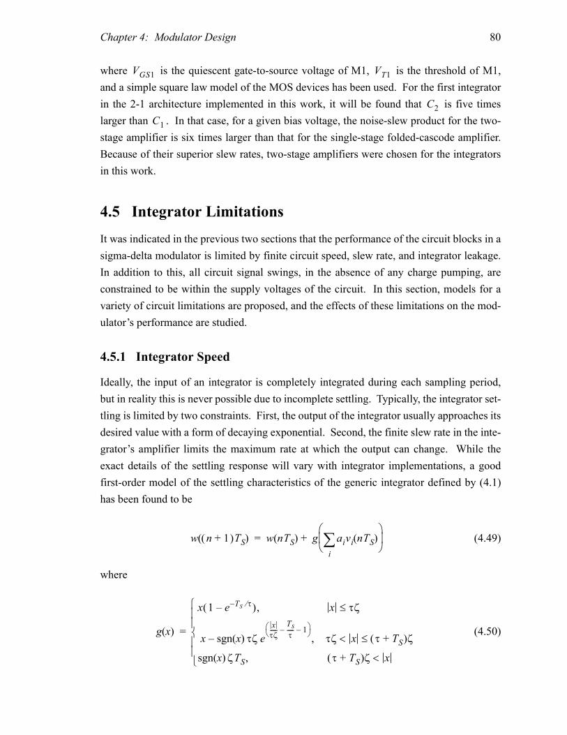
Chapter 4: Modulator Design 80
where is the quiescent gate-to-source voltage of M1, is the threshold of M1,
and a simple square law model of the MOS devices has been used. For the first integrator
in the 2-1 architecture implemented in this work, it will be found that is five times
larger than . In that case, for a given bias voltage, the noise-slew product for the two-
stage amplifier is six times larger than that for the single-stage folded-cascode amplifier.
Because of their superior slew rates, two-stage amplifiers were chosen for the integrators
in this work.
4.5 Integrator Limitations
It was indicated in the previous two sections that the performance of the circuit blocks in a
sigma-delta modulator is limited by finite circuit speed, slew rate, and integrator leakage.
In addition to this, all circuit signal swings, in the absence of any charge pumping, are
constrained to be within the supply voltages of the circuit. In this section, models for a
variety of circuit limitations are proposed, and the effects of these limitations on the mod-
ulator’s performance are studied.
4.5.1 Integrator Speed
Ideally, the input of an integrator is completely integrated during each sampling period,
but in reality this is never possible due to incomplete settling. Typically, the integrator set-
tling is limited by two constraints. First, the output of the integrator usually approaches its
desired value with a form of decaying exponential. Second, the finite slew rate in the inte-
grator’s amplifier limits the maximum rate at which the output can change. While the
exact details of the settling response will vary with integrator implementations, a good
first-order model of the settling characteristics of the generic integrator defined by (4.1)
has been found to be
(4.49)
where
(4.50)
VGS1 VT1
C2
C1
w n 1+( )TS( ) w nTS( ) g aivi nTS( )
i
∑
+=
g x( )
x 1 e TS τ⁄––( ), x τζ≤
x sgn x( ) τζ e
x
τζ-----
TS
τ----- 1––
, τζ x τ TS+( )ζ≤<–
sgn x( ) ζTS, τ TS+( )ζ x<
=
Chapter 4: Modulator Design 81
τ is the settling time constant for the integrator, and ζ is the maximum slew rate of the
amplifier. In this model, the integrator is assumed to approach its final value with a single
exponential time constant τ, but the slope of this exponential is limited to ζ. For the CDS
integrator with a two-stage amplifier, τ and ζ are approximately given by (4.44) and
(4.47), respectively.
Simulation results of a 2-1 cascaded modulator’s performance for various combina-
tions of speed limitations in the first integrator are summarized in Figure 4.10. In this
plot, contours of the signal-to-noise+distortion ratio (SNDR) for a −3 dB input are shown
as functions of the normalized slew rate and the number of settling time constants .
The normalized slew rate for the first integrator in the 2-1 architecture of Figure 4.2 is
defined to be
(4.51)
and the number of settling time constants is
(4.52)
0 2 4 6 8 10 12 14 160
1
2
3
4
5
Number of Settling Time Constants (nτ)
Norm
alized Slew Rate (
ζ N)
80 dB
90 dB
100 dB
110 dB
Figure 4.10: Integrator speed SNDR contours.
Slow Regime
Fast Regime
ζN nτ
ζN
ζTS
2af1∆1
----------------=
nτ
TS
2τ-----=
Chapter 4: Modulator Design 82
where the factor of 2 in each of these expressions is to account for the fact that in a two-
phase system only half of the sampling period is available for settling. These simulations
indicate that there are essentially two regimes in which high-resolution performance can
be achieved, denoted hereafter as the slow regime and the fast regime.
In the slow regime, no slew limiting occurs, and the settling time constant acts as an
equivalent gain error as discussed in Section 2.5. The number of settling time constants
can be as low as 3 or 4, but the normalized slew rate must be greater . If, in a
given design, the process results in circuits that are faster than expected and increases
without a corresponding increase in the , the SNDR of the modulator could actually
decrease. In other words, the slow regime depends on the settling being linear, and any
deviation from linear setting degrades the modulator’s performance.
In the fast regime, the integrator is strongly slew-rate limited, but the amplifier settling
is sufficiently fast to reduce the nonlinear effects of the slew limiting to negligible levels.
For the first integrator in the architecture of Figure 4.2, this regime occurs for . In
this regime, the normalized slew rate need only be greater than about 2, which is less than
that required in the slow regime. In contrast to the slow regime, if increases due to pro-
cess variations, the modulator performance in the fast regime is improved. Furthermore,
for the first integrator in the modulator design detailed in Chapter 5, it is easier to design a
circuit that operates in the fast regime, and therefore, a fast regime integrator has been
used.
For the second and third integrators in the 2-1 architecture, similar slow and fast
regimes exist, but their location is slightly different. In the second integrator, the fast
regime occurs for and the normalized slew rate, defined for the second integrator to
be
(4.53)
must be greater than 2.5. In the third integrator, the modulator noise shaping greatly
relaxes the speed requirements; the fast regime occurs for and the normalized slew
rate, defined for the third integrator to be
(4.54)
must be greater than 2. As is the case for the first integrator in the modulator design
detailed in Chapter 5, it is easier to design circuits for the second and third integrators that
operate in the fast regime, and therefore, fast regime integrators have been used.
nτ ζN nτ
nτ
ζN
nτ 12>
nτ
nτ 8>
ζN
ζTS
2af1ai2∆1
------------------------=
nτ 2>
ζN
ζTS
2af3∆2
----------------=

Chapter 4: Modulator Design 83
4.5.2 Integrator Leak
As discussed in Section 4.3, all practical integrator circuits exhibit integrator leak. For the
generic integrator defined by (4.1), integrator leak can be modeled by a leak parameter ε
where
(4.55)
In the z-transform domain,
(4.56)
While the effect of integrator leak has been solved exactly for a simple first-order sigma-
delta modulator [67], integrator leak in a 2-1 architecture can, to date, only be analyzed
using an approximate approach similar to that in Section 3.4.1. By replacing (4.1) with
(4.55) for the integrators in Figure 4.2, the baseband output of a 2-1 modulator architec-
ture, neglecting higher order terms, is found to be
(4.57)
If it is assumed that the quantization errors are random and uncorrelated, the total noise
power in the baseband is
(4.58)
where , , and are the leak parameters for the first, second, and third integrators,
respectively. Note that unlike many other non-idealities, the increase in baseband noise
caused by integrator leak in the second integrator, , is not attenuated by noise shaping.
If the integrator leak is to have a negligible impact on the modulator, the leak parame-
ters must satisfy the conditions
(4.59)
w n 1+( )TS( ) 1 ε–( )w nTS( ) aivi nTS( ).
i∑+=
W z( )z 1–
1 1 ε–( )z 1––--------------------------------- aiVi z( ).
i∑=
Yr z( ) Xr z( ) ε1ε2 1 z 1––( ) ε1 e2+( )+[ ]E1 z( )
G1
------------+=
1
β--- 1 z 1––( )2ε3 1 z 1––( )3+[ ]
E2 z( )
G2
------------– .
See
ε12ε2
2
M----------- ε1 ε2+( )2 π
3M3----------+
σe12
G12
--------1
β2----- ε3
2 π4
5M5----------
π6
7M7----------+
σe22
G22
--------+=
ε1 ε2 ε3
ε2
ε1 ε2, 1
β---
3
7---
π2
M2-------<
Chapter 4: Modulator Design 84
(4.60)
where it has been assumed that and are roughly of the same order of
magnitude. With = 0.5 and M = 128, and must be less than and
must be less than 0.021. For the sampled-data integrator described in Section 4.3.2, these
leak requirements correspond to a minimum amplifier gain of 1300 in the first and second
integrators in Figure 4.2, and a minimum amplifier gain of 48 in the third integrator. For
the CDS integrator described in Section 4.3.3, the minimum amplifier gain required to
meet (4.59) is reduced from 1300 to 36; in reality, however, nonlinearity concerns force
the amplifier gain to be much higher than 36.
4.5.3 Signal Swing
The final integrator limitation discussed in this section is limited signal swing in the inte-
grator circuits. As discussed in Section 3.4, a full scale, or 0-dB, input for the normalized
2-1 architecture in Figure 3.7 is a peak-to-peak swing in x of unity. From (4.3), it can be
inferred that the corresponding full-scale input to the 2-1 modulator architecture in
Figure 4.2, denoted , is a peak-to-peak swing in of
(4.61)
With the exception of some specialized transducer applications, both the peak input swing
and the D/A outputs and must be less than some maximum signal voltage
. In order that both the input and the D/A output signals will be as high above the
circuit noise floor as possible, the integrator gains and D/A outputs are chosen so that
(4.62)
In addition to limits on , , and , the integrator outputs must be less than some
clipping voltage to avoid clipping distortion in the modulator. Let the normalized
integrator outputs for the 2-1 architecture in Figure 4.2 be defined as
(4.63)
(4.64)
ε35
7---
πM-----<
σe12 G1
2⁄ σe22 G2
2⁄
β ε1 ε2 7.94–×10 ε3
vipp vi
vippaf1∆1
ai1
-------------.=
vipp ∆1 ∆2
VMAX
vipp ∆1 ∆2 VMAX.= = =
vipp ∆1 ∆2
VCLIP
w1N
w1
af1∆1
-------------=
w2N
w2
af2∆1
-------------=

Chapter 4: Modulator Design 85
(4.65)
Simulations of the maximum normalized integrator output swings for this 2-1 architecture
with moderate to full-scale sinusoidal inputs are shown in Figure 4.11. These simulations
demonstrate that as the input level approaches full-scale, the first integrator output swing
increases slightly while the second and third integrator output swings increase dramati-
cally. For input signals less than −3 dB below full-scale, the normalized first integrator
output, , is bounded by approximately 3.5, and the normalized second and third inte-
grator outputs, and , are bounded by approximately 3.
is constrained by the supply voltages and the ability of the integrator circuits to
drive their outputs close to the supply voltages. While is similarly constrained by
the supply voltages and the device technology, it is typically reduced below this system
limit so that the signal levels are small enough to avoid integrator outputs that exceed
. However, because of the rapid increase in the output swing of the second and third
integrators as the input approaches full-scale, it is impractical to restrict so that the
integrator outputs never exceed . Nonetheless, for input signals that do not overload
the modulator, the integrator outputs for the modulator in Figure 4.2 will be less than
if
w3N
w3
af3∆2
-------------.=
-10 -8 -6 -4 -2 00
2
4
6
8
10
Input Amplitude (dB)
Maximum Norm
alized Integrator Swing
First integrator (w1N)
Second integrator (w2N)
Third integrator (w3N)
Figure 4.11: Maximum integrator swings in the 2-1 architecture.
w1N
w2N w3N
VCLIP
VMAX
VCLIP
VMAX
VCLIP
VCLIP
Chapter 4: Modulator Design 86
(4.66)
(4.67)
(4.68)
4.6 Specifications for the 2-1 Modulator
In this chapter, a variety of circuit architectures have been examined for use in the imple-
mentation of a 2-1 cascaded sigma-delta modulator architecture. Based on the overall
modulator structure shown in Figure 4.2 and the analyses described in this chapter, the
topology and circuit specifications for a high-resolution sigma-delta modulator are pre-
sented in this section. First, integrator gains that maximize the dynamic range for a given
noise floor and voltage supply limits are computed. Second, the topology and basic circuit
specifications for the integrators are summarized.
4.6.1 Integrator Gains
In the 2-1 modulator architecture shown in Figure 4.2, nine design parameters must be
determined: seven integrator gains and two D/A gains. The values of b, β, and λ in (4.4)–
(4.6) are set to 2.5, 0.5, and 2.0, respectively, as chosen in Chapter 3. These equations
combined with (4.61) and (4.62) limit the degrees of freedom to three. The remaining
degrees of freedom are resolved by choosing integrator gains in conjunction with
and so that the integrator outputs do not exceed . Since, for a given noise
floor, the dynamic range is maximized by using the largest allowable in the system,
the goal in choosing the integrator gains is to insure that is not constrained by any-
thing other than the supply voltages and the device technology.
In previously reported designs, the first and second integrator gains have simply been
chosen so that = and = [31, 32]. With b = 2.5, it can then be inferred from
(4.4) that = 0.4. According to (4.66), setting equal to 0.4 requires that
However, since both and are ultimately limited by the
same supply voltage, requiring that be less than unnecessarily restricts
.
If the second integrator gains, and , are chosen independently, need not be
0.4, and can be greater than . The design approach used herein was to first
select a to ratio that best fits within the system and technology constraints,
and then choose the integrator gains , , and so that (4.66)–(4.68) are satisfied.
3.5 af1VMAX VCLIP<
3af2VMAX VCLIP<
3af3VMAX VCLIP< .
VMAX
VCLIP VCLIP
VMAX
VMAX
ai1 af1 ai2 af2
af1 af1
VMAX VCLIP 1.4.⁄< VMAX VCLIP
VMAX VCLIP
VMAX
ai2 af2 af1
VMAX VCLIP
VCLIP VMAX
af1 af2 af3

Chapter 4: Modulator Design 87
In the experimental modulator described in Chapter 5, it was assumed that it would be rea-
sonable to achieve a that was at least 70% of . Given a to ratio
of 0.7, integrator gain values that both satisfy (4.66)–(4.68) and can be readily imple-
mented are = 0.2, = 0.25, and = 0.1. By combining these integrator gains with
(4.4)–(4.6), (4.61), and (4.62), it is possible to compute the remaining integrator gains.
All of the integrator gains for the 2-1 modulator architecture in Figure 4.2 are summarized
in Table 4.1.
By abandoning the traditional design approach wherein the integrator gains are equal,
with the result in this case that the first integrator gains, and , would be 0.4, for an
approach in which the gains of the first integrator are 0.2, the allowable input signal range
for a given has been doubled. For a given dynamic range, this increases the allow-
able noise floor, which in turn relaxes the noise requirements of the circuit components.
The cost of the reduced gain in the first integrator, in addition to requiring unequal gains in
the second and third integrators, is that the input-referred noise of the second and third
integrators, as given by (4.19), is increased. However, since these noise sources undergo
at least first-order noise shaping, their influence remains negligible.
4.6.2 Circuit Specifications
In this section, the basic circuit topology and specifications for each of the three integra-
tors in Figure 4.2 are proposed, and the requirements for the remaining modulator compo-
nents are briefly mentioned. The circuit specifications are stated in terms of the
oversampling ratio, M, the sampling period, , and the maximum signal voltage .
VCLIP VMAX VCLIP VMAX
af1 af2 af3
Gain Value
0.2
0.2
0.5
0.25
0.5
0.1
0.1
Table 4.1: Integrator gain values.
ai1
af1
ai2
af2
au3
ai3
af3
ai1 af1
VCLIP
TS VMAX
Chapter 4: Modulator Design 88
So that the input-referred 1/f noise of the first integrator is reduced to negligible levels,
a correlated double sampling (CDS) topology is used. From Table 4.1, the integrator is
required to have equal input and feedback gains of 0.2. From (4.34) it can then be inferred
that = . For good slewing performance, a two-stage class A design is used for the
amplifier within the first integrator. For the integrator in Figure 4.7 and the amplifier in
Figure 4.9, if it is assumed that < ⁄ 2 and that the 1 ⁄ f noise is reduced to
negligible levels, the total baseband input-referred noise for the first stage, as given by
(4.35), (4.43), and (4.44), is bounded by
(4.69)
The baseband noise power relative to a full-scale sinusoidal input is then
(4.70)
From the integrator speed requirements, the settling time constant τ for the first integrator
must be less than ⁄ 24, and the slew rate must be
(4.71)
Finally, the integrator leak requirements coupled with the leak term for the CDS integrator
require that the amplifier gain be at least
(4.72)
but in reality, because of amplifier non-linearity, it is usually desirable to have an amplifier
gain that is significantly higher.
As discussed in Section 4.2.2, the input-referred 1 ⁄ f noise in the second integrator is
attenuated by first-order noise-shaping, so a CDS integrator is not necessary. Instead a
simple switched-capacitor sampled-data integrator is used. An input gain of 0.5 and a
feedback gain of 0.25 are used. The settling time constant τ for the second integrator must
be less than ⁄ 16, and the slew rate must be
(4.73)
To meet the integrator leak requirements, the amplifier gain in the second integrator must
be at least
C2 5C1
gm2 gm1
SN2kT
M-----------
1
C1
------5γ4CC
----------+ .<
SNR
8SN
VMAX2
-------------.=
TS
ζ 0.8VMAX
TS
-------------.>
AM
3.6------->
TS
ζ 0.5VMAX
TS
-------------.>
Chapter 4: Modulator Design 89
(4.74)
For the third integrator, as in the second integrator, a simple sampled-data integrator is
used. However, as depicted in Figure 4.2, the third integrator requires three inputs: an
input with a negative gain of 0.5, an input with a positive gain of 0.1, and a feedback gain
of 0.1. The settling time constant τ for the third integrator must be less than ⁄ 4, and the
slew rate must be
(4.75)
To meet the integrator leak requirements, the amplifier gain in the third integrator must be
at least
(4.76)
The remaining blocks in the modulator circuit, the comparators and feedback D/A
converters, have only minimal design requirements. Since the comparator noise is attenu-
ated along with the quantization noise, little attention needs to be paid to comparator non-
idealities such as dc offset and hysteresis. The primary requirement is that the comparator
be able to complete a comparison well within one clock phase, which is ⁄ 2. The D/A
converters will be implemented as switches to external voltage references, so the principle
requirement for these blocks is that the external reference have very low noise.
4.7 Summary
In a high-resolution sigma-delta modulator design, it is imperative that architecture and
circuit topologies be chosen carefully in order to obtain the widest dynamic range possible
in a given technology. In this chapter, a 2-1 cascaded sigma-delta modulator design with
many topological improvements over previous designs has been proposed. These
improvements include an architectural arrangement in which the integrator gains are cho-
sen to maximize the allowable signal levels, a correlated double sampling integrator that
attenuates the 1 ⁄ f noise in the amplifier, and a two-stage amplifier that achieves a high
slew rate. Circuit limitations, such as noise, settling time, slew rate, and integrator leak,
have been analyzed, culminating in the specification of a 2-1 modulator circuit design.
The circuit specifications are given in general terms that are intended to be applicable to
any high-resolution CMOS 2-1 architecture design. An experimental audio-band modula-
AM2
12.9----------.>
TS
ζ 0.4VMAX
TS
-------------.>
AM
2.7-------.>
TS

Chapter 4: Modulator Design 90
tor implementation based on these specifications is described in Chapter 5; this prototype
is used as a vehicle to validate much of the analyses in the preceding chapters.

90
Chapter
5 Implementation
As stated in Chapter 1, one goal of this work is the design and implementation of a
sigma-delta modulator with of a dynamic range of better than 100 dB for a signal band-
width of 25 kHz when integrated in a digital-compatible 5-V CMOS technology. Towards
this goal, the 2-1 architecture established in Chapter 4 has been implemented in a 1-µm
CMOS technology with metal-to-polycide capacitors [68]. The details of this experimen-
tal circuit and the measured test results are presented in this chapter.
The overall structure of the analog portion of the 2-1 modulator implementation is
shown in Figure 5.1. The digital components, including the error cancellation network
and the decimation filter have not been integrated; they are implemented in software. The
implementation in Figure 5.1 is basically the same as the modulator architecture shown in
Figure 4.2 with the gain values from Table 4.1, except that there is a sign reversal in the
second stage. This sign reversal is easily corrected in the error cancellation network and,
as will be discussed in Section 5.1.3, allows to sampled during the clock phase in
which it is valid.
The principle difference between the circuits topologies discussed in Chapter 4 and the
implementation described in this chapter is that the circuits in the implementation are fully
differential. A fully differential arrangement is used because of its immunity to switch
charge injection, substrate noise, supply noise, and other common-mode disturbances [49,
65]. The differential arrangement also doubles the effective signal voltages and slewing
currents. Doubling the signal voltages increases the signal power by a factor of four.
Compared to the single-ended illustrations in the previous chapter, the effective noise
power is doubled because of the two independent signal paths, so the net result is a factor
of two increase in the dynamic range of the circuits.
Throughout this chapter, the two individual components of a differential signal will be
denoted by adding an additional subscript of “p” or “m” to the differential signal name.
For example, the signal has two components and , where = − .
vf1
vi vip vim vi vip vim
Chapter 5: Implementation 91
The experimental modulator described in this chapter uses an oversampling ratio, M,
of 128, which, according to the analyses and simulations in Chapters 2 and 3, is sufficient
to reduce the quantization noise in a third-order modulator to well below the design
requirements. With a signal bandwidth of 25 kHz, this oversampling ratio corresponds to
a sampling frequency, , of 6.4 MHz and a sampling period, , of 156 ns. The maxi-
mum signal voltage, , is constrained by the single 5-V supply. So that the integrator
inputs and outputs are centered between the single 5-V supply and ground, the differential
circuits are designed to operate with a common-mode voltage, , of 2.5 V. To keep the
signal levels comfortably between the 5-V supply and ground, the signal swings were lim-
ited to ±2.0 V about , resulting in an effective differential of 8 V.
The only circuit blocks implemented in the experimental circuit but not shown explic-
itly in Figure 5.1 are the clock generators. Eight clock signals are needed in the modula-
tor, comprising four basic clock phases and the complements of those four clock phases.
The primary clock phases are two non-overlapping clocks, and , and their comple-
ments, and . From the primary clock phases, two delayed versions of the
0.2
−0.2
0.5
−0.25
0.5
−0.1
−0.1
Σ ∫ Σ ∫
Σ ∫
Q(w2)
Q(w3)
∆1
∆2
y1
−y2
vi
Integrator #1 Integrator #2
Integrator #3
w1
w2
w3
vf1
vf2
Figure 5.1: 2-1 architecture implementation.
fS TS
VMAX
VCM
VCM VMAX
φ1 φ2
φ1 φ2

Chapter 5: Implementation 92
non-overlapping clocks, and , and their complements, and , are gener-
ated. A timing diagram that illustrates , , , and is provided in Figure 5.2.
The details of the 2-1 architecture implementation, including the first, second, and
third integrators, the comparator-D/A subsystems, and the clock generators are described
in the next two sections. In the third section, measured results from this experimental cir-
cuit are presented.
5.1 The Integrators
The integrators are the most important components in the modulator circuit. Of the inte-
grators, the first integrator is the most critical. The first two subsections in this section
detail the design of the first integrator and the amplifier within the first integrator. The last
subsection then describes the remaining integrators.
φ1D φ2D φ1D φ2D
φ1 φ2 φ1D φ2D
φ1
t
t
t
t
TS ⁄ 2
φ1D
φ2
φ2D
Figure 5.2: Clock phase timing diagram.
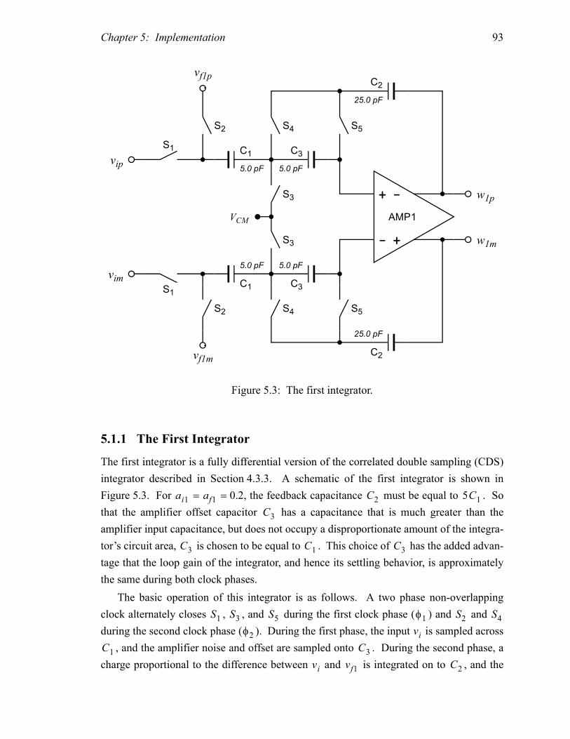
Chapter 5: Implementation 93
5.1.1 The First Integrator
The first integrator is a fully differential version of the correlated double sampling (CDS)
integrator described in Section 4.3.3. A schematic of the first integrator is shown in
Figure 5.3. For = = 0.2, the feedback capacitance must be equal to . So
that the amplifier offset capacitor has a capacitance that is much greater than the
amplifier input capacitance, but does not occupy a disproportionate amount of the integra-
tor’s circuit area, is chosen to be equal to . This choice of has the added advan-
tage that the loop gain of the integrator, and hence its settling behavior, is approximately
the same during both clock phases.
The basic operation of this integrator is as follows. A two phase non-overlapping
clock alternately closes , , and during the first clock phase ( ) and and
during the second clock phase ( ). During the first phase, the input is sampled across
, and the amplifier noise and offset are sampled onto . During the second phase, a
charge proportional to the difference between and is integrated on to , and the
AMP1
-
+
+
-
C1
5.0 pF
C1
5.0 pF
C2
25.0 pF
C2
25.0 pF
C3
5.0 pF
C3
5.0 pF
S1
S1
S2
S2
S3
S3
S4
S4
S5
S5
vim
vip
vf1m
vf1p
w1m
w1p
VCM
Figure 5.3: The first integrator.
ai1 af1 C2 5C1
C3
C3 C1 C3
S1 S3 S5 φ1 S2 S4
φ2 vi
C1 C3
vi vf1 C2
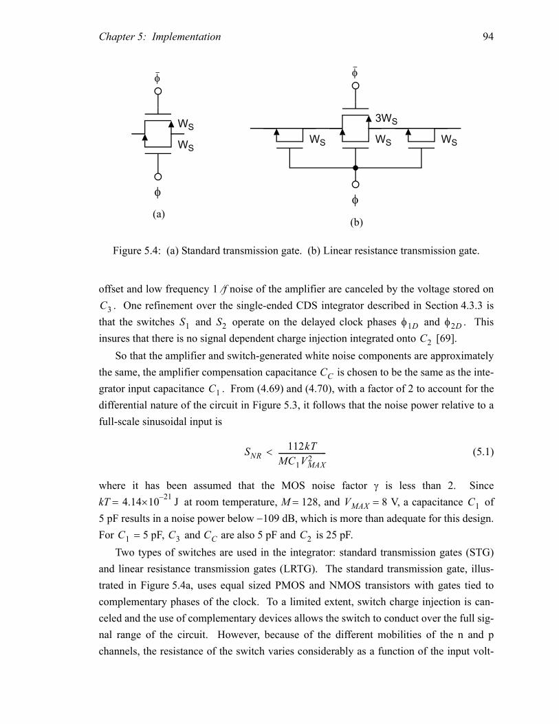
Chapter 5: Implementation 94
offset and low frequency 1 ⁄ f noise of the amplifier are canceled by the voltage stored on
. One refinement over the single-ended CDS integrator described in Section 4.3.3 is
that the switches and operate on the delayed clock phases and . This
insures that there is no signal dependent charge injection integrated onto [69].
So that the amplifier and switch-generated white noise components are approximately
the same, the amplifier compensation capacitance is chosen to be the same as the inte-
grator input capacitance . From (4.69) and (4.70), with a factor of 2 to account for the
differential nature of the circuit in Figure 5.3, it follows that the noise power relative to a
full-scale sinusoidal input is
(5.1)
where it has been assumed that the MOS noise factor γ is less than 2. Since
kT = at room temperature, M = 128, and = 8 V, a capacitance of
5 pF results in a noise power below −109 dB, which is more than adequate for this design.
For = 5 pF, and are also 5 pF and is 25 pF.
Two types of switches are used in the integrator: standard transmission gates (STG)
and linear resistance transmission gates (LRTG). The standard transmission gate, illus-
trated in Figure 5.4a, uses equal sized PMOS and NMOS transistors with gates tied to
complementary phases of the clock. To a limited extent, switch charge injection is can-
celed and the use of complementary devices allows the switch to conduct over the full sig-
nal range of the circuit. However, because of the different mobilities of the n and p
channels, the resistance of the switch varies considerably as a function of the input volt-
C3
S1 S2 φ1D φ2D
C2
CC
C1
SNR112kT
MC1VMAX2
--------------------------<
4.1421–×10 J VMAX C1
C1 C3 CC C2
φ
3WS
WS WS WS
φ
φ
WS
WS
φ
(a)(b)
Figure 5.4: (a) Standard transmission gate. (b) Linear resistance transmission gate.
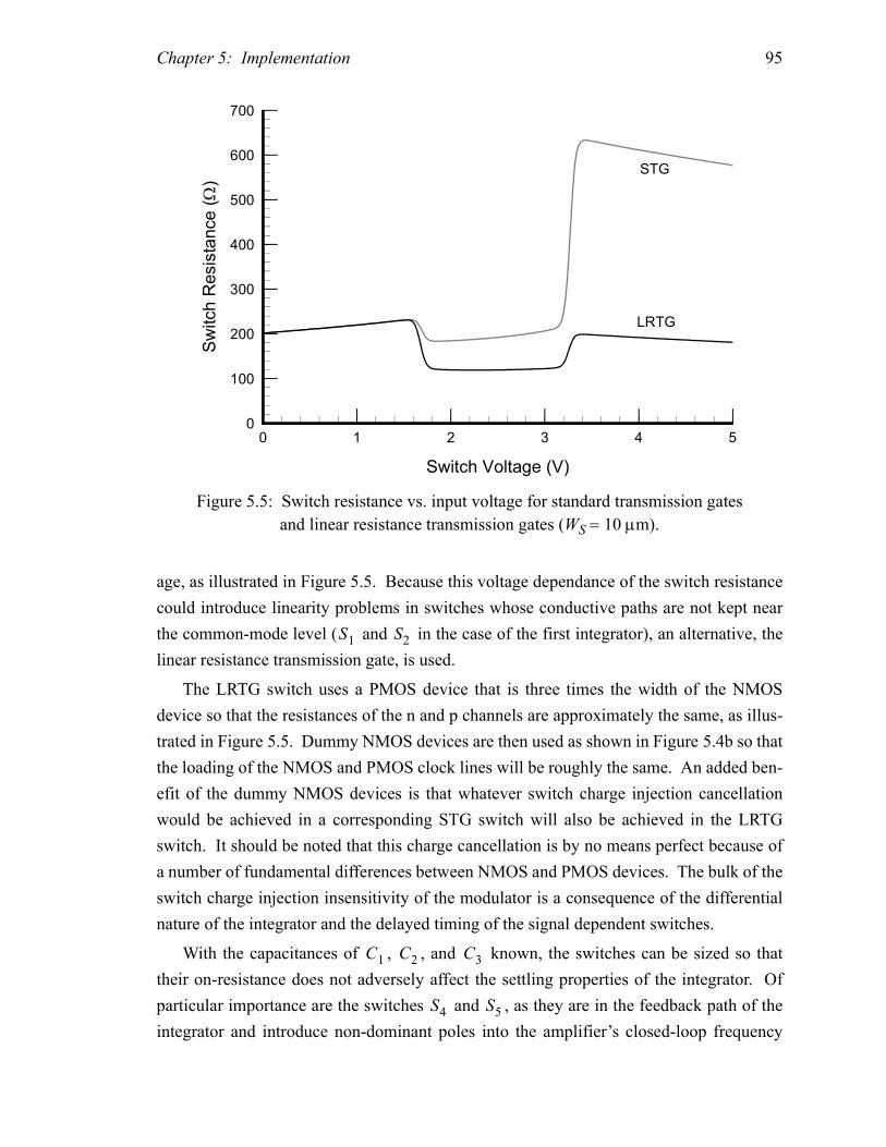
Chapter 5: Implementation 95
age, as illustrated in Figure 5.5. Because this voltage dependance of the switch resistance
could introduce linearity problems in switches whose conductive paths are not kept near
the common-mode level ( and in the case of the first integrator), an alternative, the
linear resistance transmission gate, is used.
The LRTG switch uses a PMOS device that is three times the width of the NMOS
device so that the resistances of the n and p channels are approximately the same, as illus-
trated in Figure 5.5. Dummy NMOS devices are then used as shown in Figure 5.4b so that
the loading of the NMOS and PMOS clock lines will be roughly the same. An added ben-
efit of the dummy NMOS devices is that whatever switch charge injection cancellation
would be achieved in a corresponding STG switch will also be achieved in the LRTG
switch. It should be noted that this charge cancellation is by no means perfect because of
a number of fundamental differences between NMOS and PMOS devices. The bulk of the
switch charge injection insensitivity of the modulator is a consequence of the differential
nature of the integrator and the delayed timing of the signal dependent switches.
With the capacitances of , , and known, the switches can be sized so that
their on-resistance does not adversely affect the settling properties of the integrator. Of
particular importance are the switches and , as they are in the feedback path of the
integrator and introduce non-dominant poles into the amplifier’s closed-loop frequency
0 1 2 3 4 50
100
200
300
400
500
600
700
Switch Voltage (V)
Switch Resistance (
Ω)
STG
LRTG
Figure 5.5: Switch resistance vs. input voltage for standard transmission gates
and linear resistance transmission gates (WS = 10 µm).
S1 S2
C1 C2 C3
S4 S5
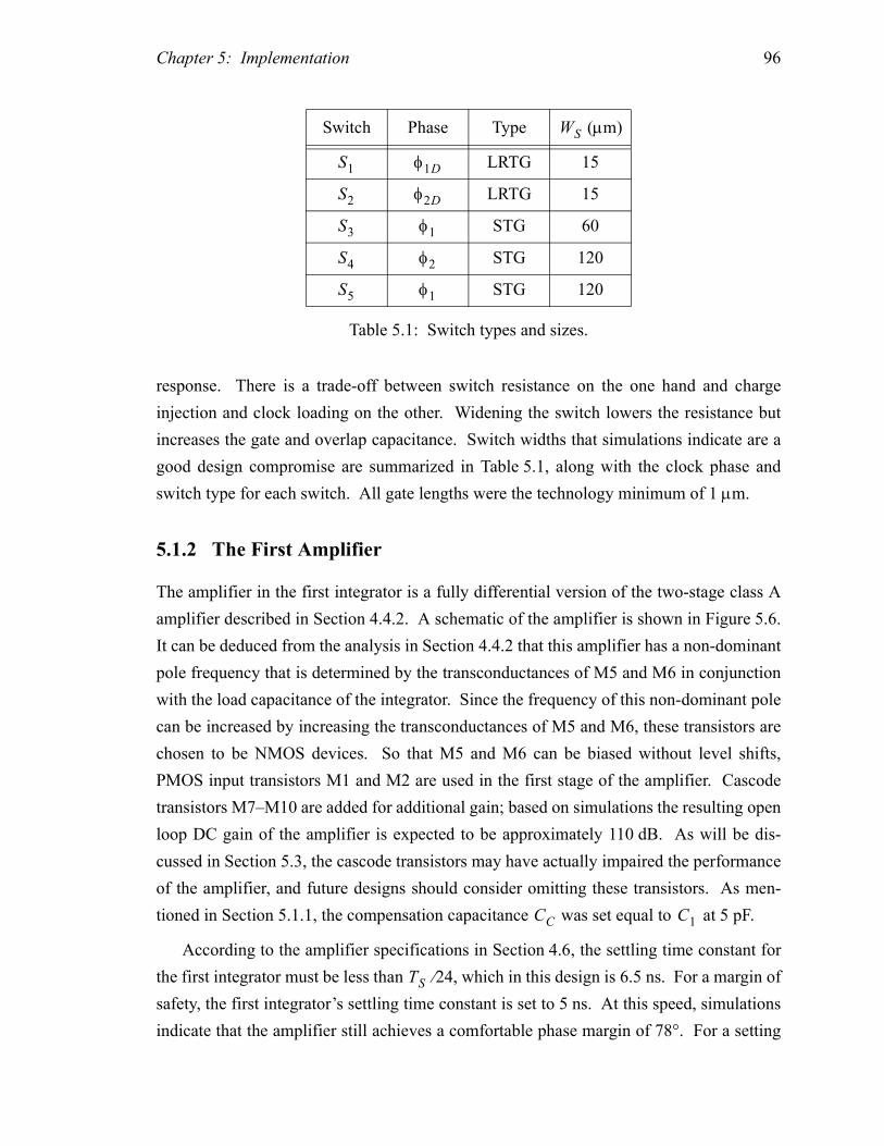
Chapter 5: Implementation 96
response. There is a trade-off between switch resistance on the one hand and charge
injection and clock loading on the other. Widening the switch lowers the resistance but
increases the gate and overlap capacitance. Switch widths that simulations indicate are a
good design compromise are summarized in Table 5.1, along with the clock phase and
switch type for each switch. All gate lengths were the technology minimum of 1 µm.
5.1.2 The First Amplifier
The amplifier in the first integrator is a fully differential version of the two-stage class A
amplifier described in Section 4.4.2. A schematic of the amplifier is shown in Figure 5.6.
It can be deduced from the analysis in Section 4.4.2 that this amplifier has a non-dominant
pole frequency that is determined by the transconductances of M5 and M6 in conjunction
with the load capacitance of the integrator. Since the frequency of this non-dominant pole
can be increased by increasing the transconductances of M5 and M6, these transistors are
chosen to be NMOS devices. So that M5 and M6 can be biased without level shifts,
PMOS input transistors M1 and M2 are used in the first stage of the amplifier. Cascode
transistors M7–M10 are added for additional gain; based on simulations the resulting open
loop DC gain of the amplifier is expected to be approximately 110 dB. As will be dis-
cussed in Section 5.3, the cascode transistors may have actually impaired the performance
of the amplifier, and future designs should consider omitting these transistors. As men-
tioned in Section 5.1.1, the compensation capacitance was set equal to at 5 pF.
According to the amplifier specifications in Section 4.6, the settling time constant for
the first integrator must be less than ⁄ 24, which in this design is 6.5 ns. For a margin of
safety, the first integrator’s settling time constant is set to 5 ns. At this speed, simulations
indicate that the amplifier still achieves a comfortable phase margin of 78°. For a setting
Switch Phase Type (µm)
LRTG 15
LRTG 15
STG 60
STG 120
STG 120
Table 5.1: Switch types and sizes.
WS
S1 φ1D
S2 φ2D
S3 φ1
S4 φ2
S5 φ1
CC C1
TS

Chapter 5: Implementation 97
time constant of 5 ns, it can be inferred from (4.44) that M1 and M2 should be sized so
that their transconductances are 1.2 mS.
The bias voltages and set the first and second stage quiescent drain currents,
which are chosen so as to meet the slew current requirements. From (4.71), the minimum
differential slew rate is 41 V ⁄ µs. The differential slew rate for this two-stage amplifier
can be found by multiplying (4.47) by a factor of two; it can be inferred from this that the
quiescent drain currents for M1–M4 must be greater than 103 µA and the quiescent drain
currents for M5–M12 must be greater than 615 µA. To provide a margin of safety, the
first-stage drain currents are set to 200 µA and the second-stage drain currents are set to
1.2 mA. The bias voltages and are set so that M5, M6, M11 and M12 remain in
saturation.
The common-mode levels in the fully-differential amplifier are established by the
common-mode feedback circuit shown in Figure 5.7. The output common-mode level is
continuously fed back through the capacitors . The common-mode level is set by the
voltages and , and the difference between these two voltages is sampled onto
the feedback capacitors through a switched capacitor network [63]. The bias network,
280
2
M1
280
2
M2
44
4
M3
44
4
M4
300
1
M5
300
1
M6
300
1
M7
300
1
M8
720
1
M9
720
1
M10
1200
1.5
M11
1200
1.5
M12
15
1
M1315
1
M14CC
5.0 pF
CC
5.0 pF
vap vam
w1p w1m
VB1
VB2 VB2
VB3 VB3
VB4 VB4
ICMF
Figure 5.6: The amplifier for the first integrator.
VB1 VB4
VB2 VB3
CF
VCMO VCMB

Chapter 5: Implementation 98
described below, sets so that is the common-mode output voltage. is
connected to the global common-mode voltage , which is 2.5 V.
The common-mode feedback controls the bias current in M1 and M2, essentially using
MF1 as the input of a common-mode amplifier [70]. This common-mode amplifier has
the same output stage and load as the differential amplifier. The common-mode ampli-
fier’s first stage comprises the input transistor MF1, the current mirror formed by MF2
and MF3, transistors M1 and M2 (which act as cascode transistors), and the active loads
M3 and M4. The transconductance of MF1 is chosen so that the unity-gain frequency of
the common-mode closed-loop circuit is less than that of the differential-mode closed-
loop circuit, insuring that the common-mode circuit has adequate phase margin. The
switches and are all STG type switches that are clocked on the delayed phases
and , respectively. These switches have gate widths of 2.5 µm and gate lengths of
1 µm.
The bias voltages – and are generated by the bias circuitry is shown in
Figure 5.8. An external current reference is applied to M21 and M22, generating the
voltage . So that the nominal common-mode feedback current, , is , M21
is sized to be one half the width of MF1. The reference current is mirrored through M23
and M24, and those currents are applied to M25-M28. M26 is sized to be 1 ⁄ 6 of M11 and
60
4
MF1
240
1
MF2
240
1
MF3
CF510 fF CF 510 fFCS250 fF CS 250 fF
S2 S2
S2 S2
S1 S1
S1 S1
w1p w1m
ICMF
VCMO VCMO
VCMB VCMB
Figure 5.7: Common-mode feedback for the first amplifier.
VCMB VCMO VCMO
VCM
S1 S2 φ1D
φ2D
VB1 VB4 VCMB
I1
VCMB ICMF 2I1

Chapter 5: Implementation 99
30 4
M21
60 1
M22
30 4
M23
30 4
M24
120
1
M25
200
1.5
M26
120
1
M27
30
1.5
M28
120
1
M29
200
1.5
M30
120
1
M31
200
1.5
M32
44 4
M33
10 1
M34
10 1
M35
50 1
M36
CB
CB1
CB2
CB3
CB4
I 1 200 µA
VCMB
VB1
VB2
VB3
VB4
Figure 5.8: First amplifier bias circuitry.

Chapter 5: Implementation 100
M12 so that the quiescent current in the second stage is . To allow M11 and M12 to
have a drain-to-source voltage lower (in magnitude) than their gate-to-source voltage,
M28 operates in the triode region. M28 is sized so that M11 and M12 still operate in satu-
ration. M25 and M27 are sized to replicate M9 and M10. The reference current is
again mirrored by M29–M32. M33 is sized the same as M3 and M4 so that the quiescent
current in those transistors is equal to . M14–M16 operate in the triode region and are
sized so that M5 and M6 operate in saturation. To limit the effect of process variations
across the integrated circuit, M25–M36 are imbedded within the amplifier in the circuit
layout.
5.1.3 The Second and Third Integrators
Since the input-referred 1 ⁄ f noise of the second and third integrators in Figure 5.1 is atten-
uated by the noise-shaping of the modulator, a noise reduction scheme such as CDS is not
needed, and the second and third integrators are implemented as fully differential versions
of the simple sampled-data integrator described in Section 4.3.2. As circuit noise is not an
issue, the feedback capacitances for the second and third integrators are arbitrarily chosen
to be 1.0 pF — a capacitance that is small compared to the feedback capacitance of the
first integrator (25 pF), but large enough to insure reliable integrator operation in the pres-
ence of parasitic capacitances.
A schematic of the second integrator is shown in Figure 5.9. The integrator operation
is as follows. During the first phase ( ), the switches , , and conduct. The input
, which is the output of the first integrator, is sampled across both and . Dur-
ing the second phase ( ), the switches , , and open and the switches , , and
conduct. A charge proportional to the difference between and is integrated
from to , and a charge proportional to is integrated from to . Thus,
the effective gain at the input is , which, with = = 0.25 pF,
is 0.5, and the effective gain at the input is , which is 0.25.
A schematic of the third integrator is shown in Figure 5.10. The integrator operation is
as follows. During the first phase ( ), the switches , , , and conduct. The
input , which is the output of the second integrator, is sampled across , and
. During the second phase ( ), the switches , , , and open and the
switches , , , and conduct. A charge proportional to the difference between
and is integrated from to , a charge proportional to the difference between
and is integrated from to , and a charge proportional to is integrated
from to . Thus the effective gain at the input is ,
6I1
I1
I1
φ1 S1 S3 S5
w1 C1A C1B
φ2 S1 S3 S5 S2 S4
S6 w1 vf1
C1A C2 w1 C1B C2
w1 C1A C1B+( ) C2⁄ C1A C1B
vf1 C1A C2⁄
φ1 S1 S3 S5 S7
w2 C1A C1B
C1C φ2 S1 S3 S5 S7
S2 S4 S6 S8
w2 vf1 C1A C2
w2 vf2 C1B C2 w2
C1C C2 w2 C1A C1B C1C+ +( ) C2⁄
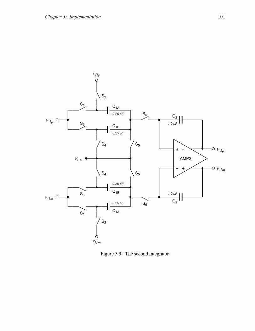
Chapter 5: Implementation 101
AMP2
-
+
+
-
C1A
0.25 pF
C1A
0.25 pF
C1B
0.25 pF
C1B
0.25 pF
C2
1.0 pF
C2
1.0 pF
S1
S1
S2
S2
S3
S3
S4
S4
S5
S5
S6
S6
w1m
w1p
vf1m
vf1p
w2m
w2p
VCM
Figure 5.9: The second integrator.

Chapter 5: Implementation 102
AMP3
-
+
+
-
C1A
0.1 pF
C1A
0.1 pF
C1B
0.1 pF
C1B
0.1 pF
C1C
0.3 pF
C1C
0.3 pF
C2
1.0 pF
C2
1.0 pF
S1
S1
S2
S2
S3
S3
S4
S4
S5
S5
S6
S6
S7
S7
S8
S8
w2m
w2p
vf1m
vf1p
vf2m
vf2p
w3m
w3p
VCM
Figure 5.10: The third integrator.

Chapter 5: Implementation 103
which, with = = 0.1 pF and = 0.3 pF, is 0.5, and the effective gain at the
and inputs are and , respectively, which are both 0.1. Note that
without the second-stage sign reversal between Figure 4.2 and Figure 5.1, the feedback
voltage would have to be sampled during the first clock phase ( ), but, as will be dis-
cussed below, the comparators are strobed during the first clock phase and do not have
valid outputs until the second clock phase ( ).
All of the switches in Figures 5.9 and 5.10 are STG types; the clock phases and gate
widths for the switches are tabulated in Tables 5.2 and 5.3. All of the switch gate lengths
were the technology minimum of 1 µm.
The amplifiers for the second and third integrators are identical, and are simply scaled
versions of the amplifier in the first integrator. The quiescent bias currents in the first and
second stages of these amplifiers are 100 µΑ and 300 µA, respectively. Schematics of the
second and third integrator’s amplifier, common-mode feedback, and bias circuitry with
the scaled device sizes are shown in Figures 5.11, 5.12, and 5.13, respectively. Because
the capacitances in the second and third integrators are much smaller than those in the first
integrator, the scaled amplifiers still exceed the speed and slew requirements specified in
Section 4.6.
C1A C1B C1C
vf1 vf2 C1A C2⁄ C1B C2⁄
vf1 φ1
φ2
Switch Phase (µm)
, 5
, 5
10
10
Table 5.2: Second integrator switches.
WS
S1 S3 φ1D
S2 S4 φ2D
S5 φ1
S6 φ2
Switch Phase (µm)
, , 5
, , 5
10
10
WS
S1 S3S5
φ1D
S2 S4S6
φ2D
S7 φ1
S8 φ2
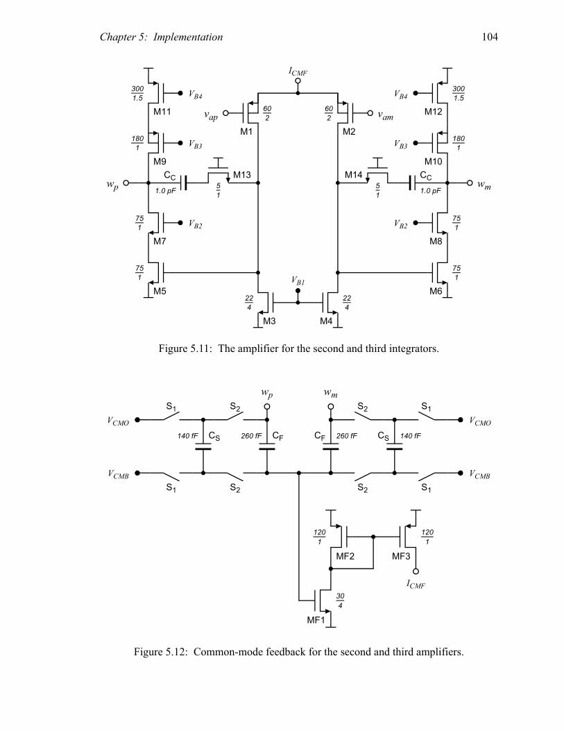
Chapter 5: Implementation 104
60
2
M1
60
2
M2
22
4
M3
22
4
M4
75
1
M5
75
1
M6
75
1
M7
75
1
M8
180
1
M9
180
1
M10
300
1.5
M11
300
1.5
M12
5
1
M135
1
M14CC
1.0 pF
CC
1.0 pF
vap vam
wp wm
VB1
VB2 VB2
VB3 VB3
VB4 VB4
ICMF
Figure 5.11: The amplifier for the second and third integrators.
30
4
MF1
120
1
MF2
120
1
MF3
CF260 fF CF 260 fFCS140 fF CS 140 fF
S2 S2
S2 S2
S1 S1
S1 S1
wp wm
ICMF
VCMO VCMO
VCMB VCMB
Figure 5.12: Common-mode feedback for the second and third amplifiers.
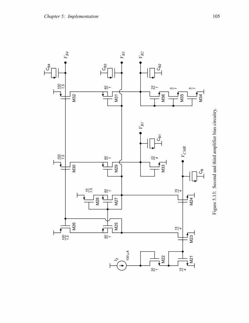
Chapter 5: Implementation 105
15 4
M21
30 1
M22
15 4
M23
15 4
M24
60 1
M25
100
1.5
M26
60 1
M27
15
1.5
M28
60 1
M29
100
1.5
M30
60 1
M31
100
1.5
M32
22 4
M33
5 1
M34
5 1
M35
25 1
M36
CB
CB1
CB2
CB3
CB4
I 2 100 µA
VCMB
VB1
VB2
VB3
VB4
Figure 5.13: Second and third amplifier bias circuitry.

Chapter 5: Implementation 106
5.2 Other Circuitry
The remaining circuit blocks in the experimental modulator are the comparator-D/A sub-
system and the clock generators. Both are described in this section.
5.2.1 Comparator-D/A Subsystem
The comparator and one-bit D/A converter are combined in a single circuit subsystem,
a block diagram of which is shown in Figure 5.14. In this figure, the thick lines indicate
differential signals. The comparator-D/A subsystem comprises five components: a differ-
COMP LATCH OUTvi vo
vfp
vfm
VFP
VFM
VFP
VFM
Figure 5.14: Comparator-D/A subsystem.

Chapter 5: Implementation 107
ential strobed comparator, a differential SR latch, a differential output buffer, and two
feedback D/A converters. When the comparator is strobed, its outputs switch regenera-
tively from a reset state to one of two digital states depending on the input. Once the com-
parator outputs reach a valid data state, that state is stored in the SR latch. The latch
outputs control the feedback D/A converters so as to switch to either or and,
correspondingly, to or . and are externally supplied dc reference
voltages. The state of the latch is also propagated outside the chip by the output buffer.
The details of the various circuits in the subsystem of Figure 5.14 are given below.
A schematic of the differential comparator is shown in Figure 5.15. As long as the
comparator strobe is high, M7 and M8 force the comparator outputs, and , to
the bottom rail (which in this design is ground); this is the reset state. When transi-
tions from high to low, the output nodes are released. Any differential voltage at the com-
parator inputs and results in a differential current being fed to the output nodes
after propagating though the current mirrors M3–M6. This current is amplified by the
regenerative feedback at M9–M12, quickly producing complementary comparison results
at the comparator outputs. The comparator strobe is driven by the clock phase so
that the comparison occurs after the integrator outputs have settled. The comparison
speed is designed to be fast enough that the entire comparator-D/A subsystem settles
before the clock phase begins.
The outputs of the comparator, and , are fed into the differential SR latch illus-
trated in Figure 5.16. The latch has inverters at each of its inputs and a core consisting of
two cross-coupled CMOS NAND gates. The input inverters are sized so that the input
threshold level is high enough to avoid false triggering when the comparator is regenerat-
ing.
The outputs of the latch, and , control the feedback D/A converters and the out-
put buffer. A schematic of one of the feedback D/A converters is shown in Figure 5.17.
In this circuit, transistors M9 and M10 act as switches between the analog output, , and
the positive and negative reference voltages, and . and are set to
± 2.0 V, that is, 4.5 V and 0.5 V, respectively. The gates of M9 and M10 are inde-
pendently driven by two-inverter buffers that serve two purposes. First, they buffer the
latch output from the large gate capacitances of M9 and M10. Second, they are sized so
that M9 and M10 never conduct simultaneously, even during a latch output transition.
Specifically, M1 and M2 are sized so that a falling edge at propagates faster than a ris-
ing edge, and M5 and M6 are sized so that a rising edge at propagates faster than a fall-
ing edge.
vfp VFP VFM
vfm VFM VFP VFP VFM
φC vcp vcm
φC
vip vim
φC φ1D
φ2
vcp vcm
vlp vlm
vf
VFP VFM VFP VFM
VCM
vl
vl
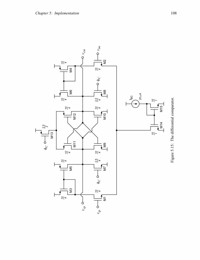
Chapter 5: Implementation 108
10 4
M1
10 4
M2
10 4
M3
10 4
M4
10 4
M5
10 4
M6
2.5 4
M7
2.5 4
M8
10 4
M9
10 4
M10
10 4
M11
10 4
M12
2.5 2
M13 10 1
M14
10 1
M15
I BC
20 µA
v ip
v im
v cp
v cm
φ C
φ Cφ C
Figure 5.15: The differential comparator.

Chapter 5: Implementation 109
2.5 4
M1
2.5 4
M2
2.5 1
M3
2.5 1
M4
10 1
M5
10 1
M6
10 1
M7
10 1
M8
2.5 1
M9
2.5 1
M10
2.5 1
M11
2.5 1
M12
v cp
v cm
v lp
v lm
Figure 5.16: The differential SR latch.

Chapter 5: Implementation 110
2.5
6
M1
15
1
M2
10
1
M3
25
1
M4
5
1
M5
2.5
2.5
M6
10
1
M7
25
1
M8
80
1
M9
200
1
M10
vl vf
VFP
VFM
Figure 5.17: The feedback D/A converter.

Chapter 5: Implementation 111
The final circuit in the comparator-D/A subsystem is the output buffer. Previous mod-
ulator designs have exhibited a sensitivity to signal-dependent substrate coupling through
the output buffers and pads [71]. To minimize the signal dependent bounce, the modulator
outputs are generated as currents that are converted off-chip to voltages by discrete, low-
impedance amplifiers. A schematic of the complete output interface for one modulator
output, including both the on- and off-chip circuits, is shown in Figure 5.18. The local
feedback around Q1 and Q2 produces a very low impedance at the bases of Q1 and Q2.
The latch output causes current to flow through one of the two transistors M1 or M2. This
current is translated into a voltage at the collectors of Q1 and Q2, which in turn controls
the differential pair formed by Q5 and Q6. The output of one side of the differential pair is
applied to a high-speed optocoupler, and the optocoupler output is fed to a data buffer for
storage and processing.
5.2.2 Clock Generators
The basic structure of the clock generator circuitry is illustrated in Figure 5.19. An off-
chip reference clock, , drives a cross-coupled pair of NOR gates. The cross-coupling
network uses inverter chains to generate delays. All gates are fully differential as
described below with the exception of the inverter at the input of NOR1, which is actually
an implicit inversion accomplished by cross-coupling the differential signal. Because all
of the switches in the integrators are CMOS transmission gates, complementary clock sig-
nals are needed for all clock phases. In contrast to a single-ended design, the fully differ-
ential clock circuits generate the complementary clock phases without requiring an
inverter between a clock phase and its complement; such an inverter would introduce
clock skew between the clock phase and its complement. In addition, the fully differential
arrangement reduces the substrate noise injection from the clock circuitry.
The non-overlapping clocks are generated as follows. Consider the case in which
is high and is low. When the clock reference, , transitions from low to high, the out-
put of NOR2, , is forced low. also remains low temporarily because one of the
inputs to NOR1, , is still high. After two inverter delays, goes low, forcing
high. Because of these inverter delays, and are never simultaneously high, and
thus, as desired, they are non-overlapping.
As an example of the fully differential CMOS topology used in the clock generators,
the schematic of a fully differential NOR gate is shown in Figure 5.20. The core of the
differential NOR gate is formed by two single-ended CMOS gate cores, a CMOS NOR
gate formed by M3, M5, M7, and M9, and a CMOS NAND gate formed by M4, M6, M8,
φR
φ2
φ1 φR
φ2 φ1
φ2D φ2D φ1
φ1 φ2
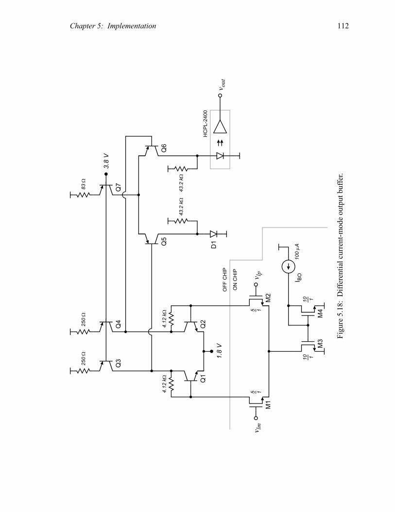
Chapter 5: Implementation 112
5 1
M1
5 1
M2
10 1
M3
10 1
M4
Q1
Q2
Q3
Q4
Q5
Q6
Q7
4.12 k
Ω4.12 k
Ω
250 Ω
250 Ω
83 Ω
43.2 k
Ω43.2 k
Ω
D1
HCPL-2400
I BO
100 µA
v lm
v lp
v out
1.8 V
3.8 V
OFF CHIP
ON CHIP
Figure 5.18: Differential current-mode output buffer.
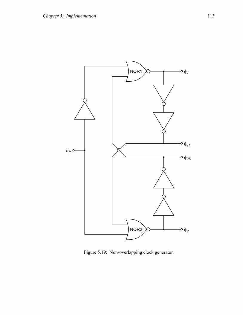
Chapter 5: Implementation 113
NOR1
NOR2
φR
φ1
φ2
φ1D
φ2D
Figure 5.19: Non-overlapping clock generator.

Chapter 5: Implementation 114
M1 M2
M3
M4
M5
M6
M7
M8
M9
M10
M11 M21
vap
vam
vbp
vbm
vop vom
Figure 5.20: Differential NOR gate.

Chapter 5: Implementation 115
and M10. The positive phase inputs are fed into the NOR gate and produce the positive
component of the NOR output, . The negative phase inputs are fed into the NAND
gate and produce the negative, or complementary, component of the NOR output, .
The transistors M1, M2, M11, and M12 form a feedback network that tends to attenuate
any clock skew that existed between the inputs and their complements.
5.3 Experimental Results
The 2-1 sigma-delta modulator circuit described in Sections 5.1 and 5.2 has been inte-
grated in a 1-µm CMOS technology; a photomicrograph of the modulator is shown in
Figure 5.21. The active circuitry occupies an area of 5.2 mm2. The performance of the
modulator was evaluated by driving its input with a high-quality differential sinusoidal
signal source [72], acquiring the one-bit output code from each of the two stages in the
modulator, and transferring the acquired data to a workstation for subsequent processing.
Decimation filtering and signal analysis were performed as described in Section 1.2 using
the same software that was used in simulations of the modulator. Full details of the test
setup are given in Chapter 6.
The modulator operates from a single 5-V supply. The differential reference voltage is
8 V, and the chip dissipates 47 mW. The sampling frequency is 6.4 MHz and the oversam-
pling ratio is 128, yielding an equivalent Nyquist sampling rate of 50 kHz and a signal
bandwidth of 25 kHz. Plots of the signal-to-noise ratio (SNR) and signal-to-noise+distor-
tion ratio (SNDR) for a 2-kHz sinusoidal input are shown in Figure 5.22. An input level
of 0 dB corresponds to a sinusoidal input whose peak-to-peak differential voltage is equal
to the differential reference voltage of 8 V. As is evident from Figure 5.22, the modulator
achieves a dynamic range of 104 dB and a peak SNDR of 98 dB. The measurement
results are summarized in Table 5.4.
Degradation in the SNDR at inputs above 5 dB is believed to be caused by distortion
in the amplifiers. While the amplifier transistors are theoretically always in saturation,
large signal swings in the amplifiers cause the cascode transistors, such as M7–M10 in
Figure 5.6, to operate near the triode region. As a consequence, these devices have a
highly nonlinear output resistance for large signals. This effect can be offset by increasing
the supply voltage, which increases the headroom between the drains of the cascode tran-
sistors and allows these transistors to operate well within the saturation region. As shown
in Figure 5.23, measurements with a 6-V supply demonstrate significantly less SNDR
degradation at high signal levels. As the extra small-signal gain provided by the cascode
vop
vom

Chapter 5: Implementation 116
Figure 5.21: Die photomicrograph of the 2-1 architecture implementation.
(die photo here)
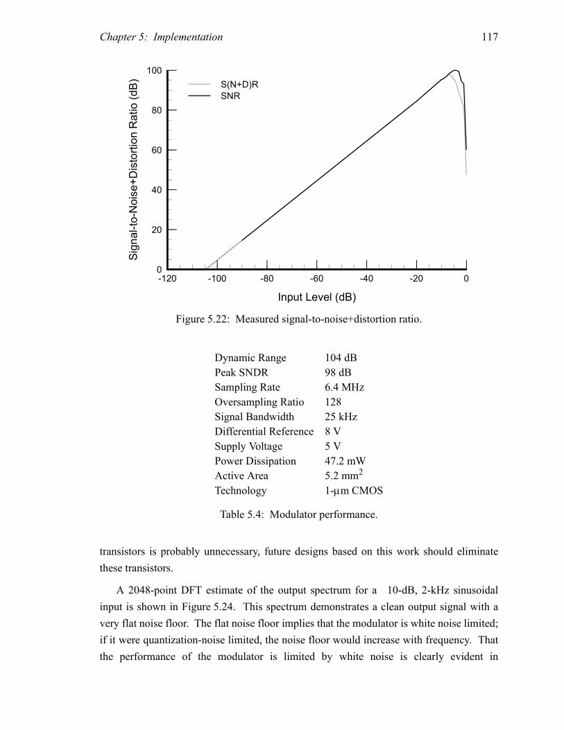
Chapter 5: Implementation 117
transistors is probably unnecessary, future designs based on this work should eliminate
these transistors.
A 2048-point DFT estimate of the output spectrum for a 10-dB, 2-kHz sinusoidal
input is shown in Figure 5.24. This spectrum demonstrates a clean output signal with a
very flat noise floor. The flat noise floor implies that the modulator is white noise limited;
if it were quantization-noise limited, the noise floor would increase with frequency. That
the performance of the modulator is limited by white noise is clearly evident in
-120 -100 -80 -60 -40 -20 00
20
40
60
80
100
Input Level (dB)
Signal-to-Noise+Distortion Ratio (dB)
S(N+D)R
SNR
Figure 5.22: Measured signal-to-noise+distortion ratio.
Dynamic Range 104 dB
Peak SNDR 98 dB
Sampling Rate 6.4 MHz
Oversampling Ratio 128
Signal Bandwidth 25 kHz
Differential Reference 8 V
Supply Voltage 5 V
Power Dissipation 47.2 mW
Active Area 5.2 mm2
Technology 1-µm CMOS
Table 5.4: Modulator performance.
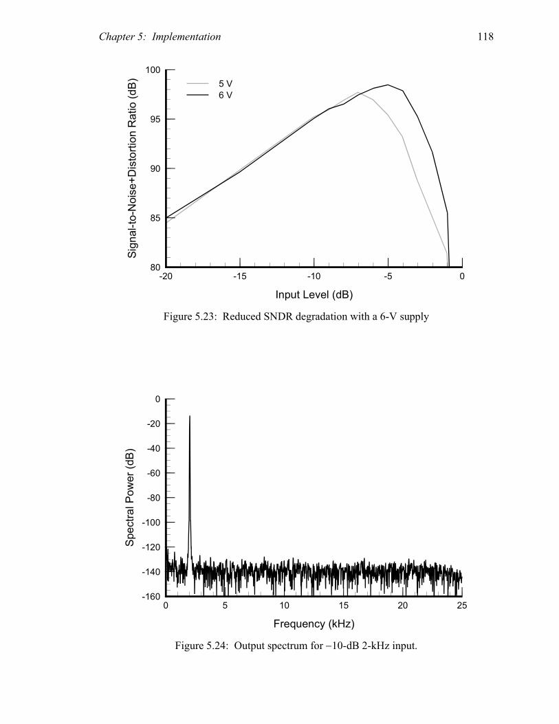
Chapter 5: Implementation 118
-20 -15 -10 -5 080
85
90
95
100
Input Level (dB)
Signal-to-Noise+Distortion Ratio (dB)
5 V
6 V
Figure 5.23: Reduced SNDR degradation with a 6-V supply
0 5 10 15 20 25-160
-140
-120
-100
-80
-60
-40
-20
0
Frequency (kHz)
Spectral Power (dB)
Figure 5.24: Output spectrum for −10-dB 2-kHz input.

Chapter 5: Implementation 119
Figure 5.25, where the measured dynamic range of the modulator is plotted as a function
of the oversampling ratio. When a third-order sigma-delta modulator is quantization noise
limited, the dynamic range increases 21 dB per octave increase in the oversampling ratio,
as indicated by (2.25). In the white noise limit, the dynamic range increases only 3 dB per
octave increase in the oversampling ratio, as given in (4.69). For oversampling ratios
below 64, this modulator is quantization noise limited, and for oversampling ratios above
64, this modulator is white noise limited. At the intended operating oversampling ratio of
128, the modulator is clearly white noise limited, implying that its performance is limited
by circuit noise.
The noise power calculations in Section 5.1 estimated that the noise power relative to
full scale would be less than 109 dB, but measurements of the experimental modulator
show a noise power relative to full scale of approximately 105 dB. The source of the
additional noise eluded discovery, but there are several facts about this additional noise
that have been determined. The most important of these is that the additional noise source
is somehow related to the slope of the input clock edge. When the rise and fall times of
the off-chip clock reference are increased from 5 ns to 20 ns, there is a 2–3 dB drop in the
noise power. Unfortunately, the slow clock edges cause the ostensibly non-overlapping
clock phases to overlap, resulting in increased distortion at high signal levels. The noise
power is also reduced when the signal swing of the clock is reduced from full 0–5 V
Quantization Limited
White Noise Limited
Figure 5.25: Measured dynamic range versus oversampling ratio.
4 5 6 7 8 950
60
70
80
90
100
110
120
130
Oversampling Ratio
Dynamic Range (dB)
l
l
l
l
ll
l ll l
l
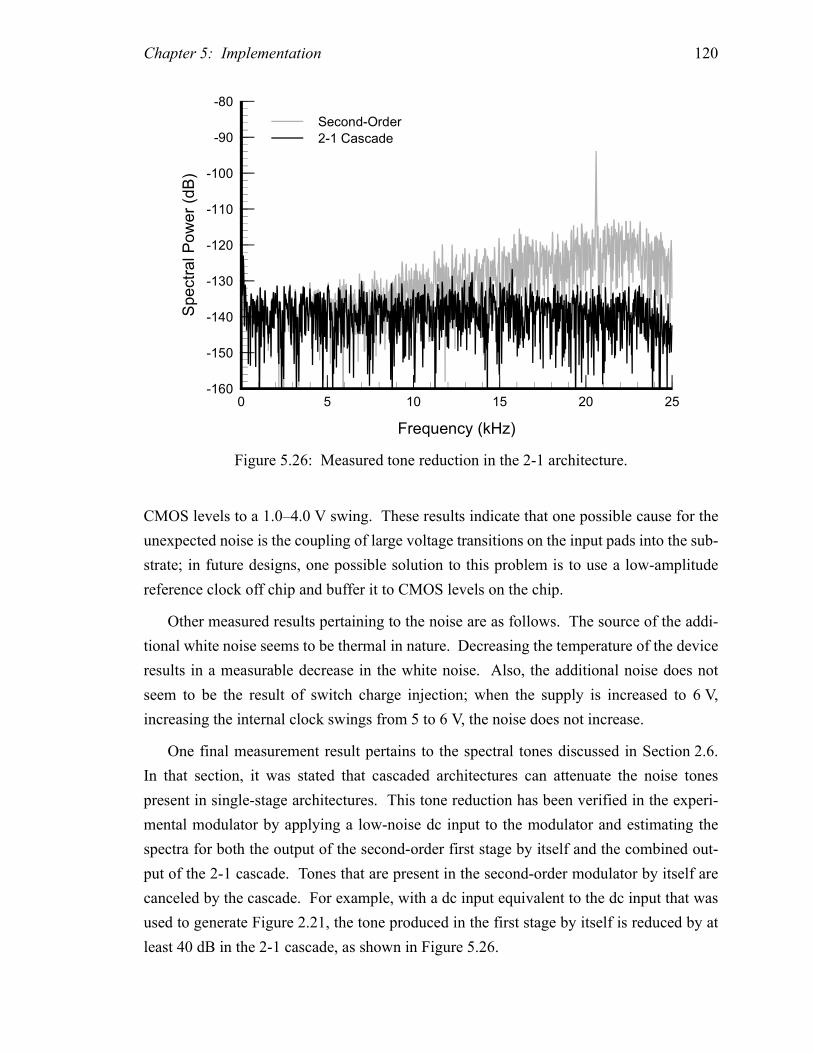
Chapter 5: Implementation 120
CMOS levels to a 1.0–4.0 V swing. These results indicate that one possible cause for the
unexpected noise is the coupling of large voltage transitions on the input pads into the sub-
strate; in future designs, one possible solution to this problem is to use a low-amplitude
reference clock off chip and buffer it to CMOS levels on the chip.
Other measured results pertaining to the noise are as follows. The source of the addi-
tional white noise seems to be thermal in nature. Decreasing the temperature of the device
results in a measurable decrease in the white noise. Also, the additional noise does not
seem to be the result of switch charge injection; when the supply is increased to 6 V,
increasing the internal clock swings from 5 to 6 V, the noise does not increase.
One final measurement result pertains to the spectral tones discussed in Section 2.6.
In that section, it was stated that cascaded architectures can attenuate the noise tones
present in single-stage architectures. This tone reduction has been verified in the experi-
mental modulator by applying a low-noise dc input to the modulator and estimating the
spectra for both the output of the second-order first stage by itself and the combined out-
put of the 2-1 cascade. Tones that are present in the second-order modulator by itself are
canceled by the cascade. For example, with a dc input equivalent to the dc input that was
used to generate Figure 2.21, the tone produced in the first stage by itself is reduced by at
least 40 dB in the 2-1 cascade, as shown in Figure 5.26.
0 5 10 15 20 25-160
-150
-140
-130
-120
-110
-100
-90
-80
Frequency (kHz)
Spectral Power (dB)
Second-Order
2-1 Cascade
Figure 5.26: Measured tone reduction in the 2-1 architecture.
Chapter 5: Implementation 121
5.4 Summary
The 2-1 cascaded modulator architecture established in Chapter 4 has been successfully
integrated in a 1-µm CMOS technology without error correction or component trimming.
This architecture has proven to be tolerant of mismatch errors in that no performance deg-
radation can be attributed to component mismatch. At a signal bandwidth of 25 kHz, the
modulator exceeds the design goal of a 100-dB dynamic range, achieving a dynamic range
of 104 dB. This wide dynamic range is attained in part by using fully differential topolo-
gies throughout the modulator. With tone reduction capabilities that reduce the unwanted
spectral tones in the second-order first stage by at least 40 dB and a dynamic range equiv-
alent to that of a 17-bit Nyquist-rate converter, this 2-1 cascaded modulator is suitable for
use as a high-performance audio-band A/D converter.

122
Chapter
6 Test Setup
Because of its wide dynamic range, testing of the experimental sigma-delta modulator
described in Chapter 5 required as much care as its design. The test setup, constructed
from custom PC boards in conjunction with high performance test equipment, is described
in detail in this chapter.
The basic organization of the test setup is shown in Figure 6.1, and the instruments in
that figure are identified in Table 6.1. The input to the device under test (DUT) is gener-
ated by a high-performance audio signal generator. The bias voltages and currents for
both the analog and digital portions of the DUT are generated with custom low-noise bias
generators that are independently driven by stand-alone DC power supplies. The two out-
put bits of the modulator are passed through a serial-to-parallel converter and then stored
in the digital analysis system (DAS). The data is then downloaded to a UNIX workstation
for processing. The system clocks are generated by a pulse generator that is locked to a
precision RF signal source. Details of the various components of the test system are
described below.
The modulator input is generated by a low-distortion balanced sinewave generator.
The balanced output and common lines of this generator are floating with respect to earth
ground and are connected to the DUT board though a three conductor shielded audio cable
with a 100% foil shield (Belden 8771). The common line is connected to the common
mode voltage , and the shield is connected to the DUT board ground. The output of
the sinewave generator is terminated on the DUT board by the one-pole low pass filter
shown in Figure 6.2. The bandlimiting provided by the 1 nF capacitors would be insuffi-
cient for a general input, but in this case the out-of-band noise produced by the signal
source is already low enough that the 1 nF capacitors are sufficient to prevent measurable
aliasing of the signal source noise into the baseband. Polystyrene capacitors are used as
they introduce less distortion than other types of capacitors. It is especially important to
VCM
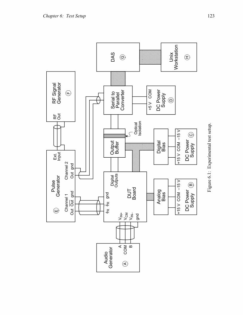
Chapter 6: Test Setup 123
AAudio
Generator
DUT
BoardPulse
Generator
RF Signal
Generator
Output
Buffer
Serial to
Parallel
Converter
DAS
Unix
Workstation
Analog
Bias
Digital
Bias
VIN+
VCM
VIN–
gnd
φ Rφ R
gnd
Digital
Outputs
+5 V
COM
Optical
Isolation
OutOutgnd
Outgnd
DC Power
Supply
DC Power
Supply
+15 V
COM
–15 V
BDC Power
Supply
+15 V
COM
–15 V
C
Ext.
Input
RF
Out
E
F
G
D
H
A
COM B
Channel 1
Channel 2
Figure 6.1: Experim
ental test setup.

Chapter 6: Test Setup 124
avoid the use ceramic chip capacitors at the input as they produce measurable distortion at
high signal levels.
The bias voltages and currents are generated by low-noise sources on custom PC
boards. Two types of boards were constructed: voltage generator boards and current gen-
erator boards. The analog bias drivers depicted in Figure 6.1 comprise one voltage bias
board and one current bias board, both connected to a ±15 V power supply that is floating
with respect to its earth ground. The common terminal of the power supply is connected
to the voltage and current bias board grounds, which are in turn connected to the DUT
board ground. The digital bias drivers are contained on one voltage bias board that is con-
nected to a separate ±15 V power supply that is also floating with respect to its earth
ground. The common terminal of that power supply is connected to the ground on the dig-
ital bias board, which in turn is connected to the DUT board ground.
A: Panasonic VP-7214A RC Oscillator
B: Hewlett-Packard 6237B Triple Output Power Supply
C: Hewlett-Packard 6236A Triple Output Power Supply
D: Harrison 6200B DC Power Supply
E: Hewlett-Packard 8130A 300 MHz Pulse Generator
F: Hewlett-Packard 8640B Signal Generator
G: Tektronix DAS 9200 Digital Analysis System with 92A90 Retargetable Buffer Probe
H: Digital DECstation 3100 with IOTech SCSI 488/D Bus Controller
Table 6.1: Test setup equipment list.
vsrc
+
-
vsrc
+
-
300 Ω
300 Ω
150 Ω
150 Ω
150 Ω
150 Ω
1 nF
1 nF
vip
vim
VCM
VP-7214A
Figure 6.2: Differential sinewave generator load circuit.
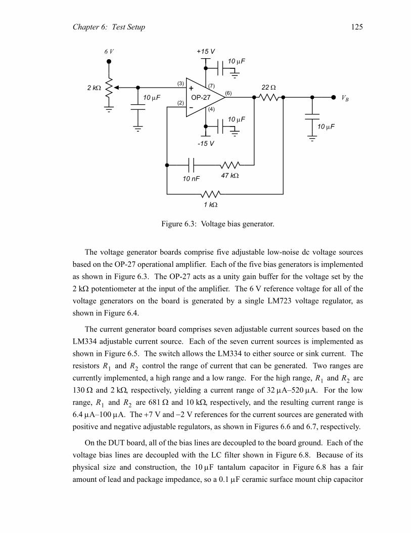
Chapter 6: Test Setup 125
The voltage generator boards comprise five adjustable low-noise dc voltage sources
based on the OP-27 operational amplifier. Each of the five bias generators is implemented
as shown in Figure 6.3. The OP-27 acts as a unity gain buffer for the voltage set by the
2 kΩ potentiometer at the input of the amplifier. The 6 V reference voltage for all of the
voltage generators on the board is generated by a single LM723 voltage regulator, as
shown in Figure 6.4.
The current generator board comprises seven adjustable current sources based on the
LM334 adjustable current source. Each of the seven current sources is implemented as
shown in Figure 6.5. The switch allows the LM334 to either source or sink current. The
resistors and control the range of current that can be generated. Two ranges are
currently implemented, a high range and a low range. For the high range, and are
130 Ω and 2 kΩ, respectively, yielding a current range of 32 µA–520 µA. For the low
range, and are 681 Ω and 10 kΩ, respectively, and the resulting current range is
6.4 µA–100 µA. The +7 V and −2 V references for the current sources are generated with
positive and negative adjustable regulators, as shown in Figures 6.6 and 6.7, respectively.
On the DUT board, all of the bias lines are decoupled to the board ground. Each of the
voltage bias lines are decoupled with the LC filter shown in Figure 6.8. Because of its
physical size and construction, the 10 µF tantalum capacitor in Figure 6.8 has a fair
amount of lead and package impedance, so a 0.1 µF ceramic surface mount chip capacitor
10 nF
+
-
OP-27(2)
(3) (7)
(4)
(6)2 kΩ
1 kΩ
47 kΩ
22 Ω
10 µF
10 µF
10 µF10 µF
VB
6 V +15 V
-15 V
Figure 6.3: Voltage bias generator.
R1 R2
R1 R2
R1 R2

Chapter 6: Test Setup 126
is mounted as close to the DUT as possible to provide a low impedance path to the DUT
board ground plane. Each of the current sources are similarly bypassed on the DUT board
with the RC filter shown in Figure 6.9.
A discrete output buffer for each modulator output, illustrated in Figure 5.18, is imple-
mented on the output buffer board shown in Figure 6.1. As indicated in Figure 5.18, the
+
-
7 V ref.
(2)
(3)
(4)
(5)
(6)
(7)
(10)
(11)(12)LM723
1 kΩ
5.6 kΩ
825 Ω
10 Ω
5 µF
100 pF6 V
+15 V
Figure 6.4: 6 V voltage reference.
V+
R
V-
LM334
R1
R2
+7 V
-2 V
IOUT
SOURCE SINK
Figure 6.5: Current generators.
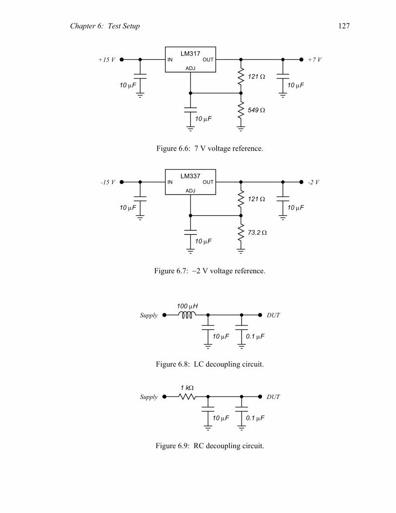
Chapter 6: Test Setup 127
IN
ADJ
OUTLM317
121 Ω
549 Ω
10 µF
10 µF
10 µF
+15 V +7 V
Figure 6.6: 7 V voltage reference.
IN
ADJ
OUTLM337
121 Ω
73.2 Ω
10 µF
10 µF
10 µF
-15 V -2 V
Figure 6.7: −2 V voltage reference.
100 µH
10 µF 0.1 µF
Supply DUT
Figure 6.8: LC decoupling circuit.
Figure 6.9: RC decoupling circuit.
1 kΩ
10 µF 0.1 µF
Supply DUT
Chapter 6: Test Setup 128
modulator outputs are optically isolated from the digital data acquisition hardware to
prevent ground noise in that hardware from corrupting the modulator’s ground plane.
Each of the one-bit, 6.4 MHz modulator outputs is converted to a 32-bit, 200 kHz output
word by a serial-to-parallel converter. The serial-to-parallel converter for each output
comprises four TTL 8-bit serial-to-parallel shift registers (SN74164) clocked in parallel
into four TTL 8-bit D-type latches (SN74377). The 32-bit output derived from each mod-
ulator output is collected by the 92A90 buffer probe on the DAS. This buffer is 32 K
deep, allowing over one million output bits to be collected from each of the two modulator
outputs. Once the modulator output data has been acquired by the DAS buffer, it is trans-
ferred through the IEEE 488 bus to a workstation for subsequent processing.
The modulator and acquisition clocks are produced by a two-channel pulse generator
that is locked to a precision RF signal generator. The ground of the pulse generator is con-
nected to the DUT board ground and is the only earth ground connection for the entire
analog portion of the test setup. The use of the RF signal generator greatly reduces the
phase noise in the pulse generator output.
The modulator clock is fully differential and is driven by the output and complemen-
tary output of one channel from the pulse generator. This clock is nominally set to have a
pulse width of 78.1 ns, rise and fall times of 5 ns, and high and low clock levels of 4 V and
1 V, respectively. The clock is connected to the DUT board through a balanced triaxial
cable (Belden 9272). Each of the two differential clock lines is terminated to the DUT
board ground by a 50 Ω surface mount resistor located adjacent to the DUT.
The second channel of the pulse generator produces the acquisition clock that is used
to clock the serial-to-parallel converter, which in turn clocks the DAS. Like the modulator
clock, the acquisition clock is set to have a pulse width of 78.1 ns and rise and fall times of
5 ns; however, the acquisition clock is delayed with respect to the modulator clock to com-
pensate for the propagation delay though the modulator and its output buffer. With a
6.4 MHz clock having 5 ns rise and fall times, the appropriate delay is approximately
20 ns. The output levels of the acquisition clock are set to 3.5 V and 0 V to be compatible
with the TTL integrated circuits used to implement the serial-to-parallel converters.
The DUT itself is packaged in a PLCC package with very low lead inductance
(approximately 10 nH at each pin). Other research has shown that multiple ground pins
can further reduce the noise induced on the substrate [73]; therefore, several ground pins
were included in the chip layout. It turned out that in this prototype, multiple ground pins
were not required; removing all but one ground bond wire produced no degradation in the
modulator performance. The insensitivity of the circuit to the number of ground pads is
most likely a consequence of its differential topology. Designs that incorporate large

Chapter 6: Test Setup 129
amounts of single-ended digital circuitry should carefully consider the number of ground
pads to be used.
The modulator circuit itself employs separate and ground lines for the analog and
digital circuitry. Specifically, the analog and ground are connected to the integrators,
and the digital and ground lines are connected to the clock generators and the com-
parator-D/A subsystems. The substrate in the analog circuitry is tied directly to the analog
ground, while the substrate in the digital circuitry is tied to a separate substrate ground that
is connected to the analog ground on chip at the chip periphery.
The test setup described in this chapter has made it possible to repeatedly reproduce
measurements of the modulator. The total effective input referred noise voltage of the test
setup is less than 20 µV rms, and measurements taken months apart indicated little drift in
the setup. This repeatability is attributed to the use of custom printed circuit (PC) boards
rather than wire-wrap, breadboard, or other test board techniques. PC boards create a
clean layout with a good ground plane, and the time taken to produce the PC boards is
more than compensated by the time saved in testing.
VDD
VDD
VDD
130
Chapter
7 Conclusion
The use of sigma-delta modulation to achieve high-resolution A/D conversion in a
VLSI technology has gained wide acceptance in the engineering community. Applica-
tions employing sigma-delta modulation range from high-performance multi-chip mod-
ules in which the analog portion of the modulator occupies an entire chip to single-chip
systems in which the analog portion of the modulator occupies only a small fraction of the
total chip area. As the use of sigma-delta modulation becomes more commonplace, it is
important that the principles of sigma-delta modulation be well understood and that the
performance limits of sigma-delta modulators be discovered.
This work has sought to extend the understanding of sigma-delta modulation in three
principle areas: the analysis of cascaded architectures, the modeling of sigma-delta modu-
lators, and the design of high-resolution modulators.
In the area of cascaded architectures, a comparison of third-order cascaded sigma-
delta modulators using a simplified unity gain approximation indicates that the cascade of
a second-order modulator followed by a first-order modulator (the 2-1 architecture) is
much less sensitive to matching errors in the modulator circuit than a cascade of three
first-order modulators (the 1-1-1 architecture). With the 2-1 architecture, it is possible to
achieve high-resolution A/D conversion without stringent component matching require-
ments. In addition, the 2-1 architecture greatly attenuates the coloration in the quantiza-
tion error spectrum that can be present in single-stage architectures.
When the unity gain approximation yields an insufficient characterization of a sigma-
delta modulator architecture, the adaptive gain model can provide a more accurate repre-
sentation. This model uses a combination of describing function analysis, analytical mod-
eling, and empirical approximation to accurately estimate the baseband quantization noise
power as a function of the input signal level. Through this model, it is possible to charac-
terize both the low level and the overload performance of sigma-delta modulators.

Chapter 7: Conclusion 131
In this work, the adaptive gain model has been applied to a 2-1 cascaded architecture
in order to determine the architectural parameter values for a high-resolution audio-band
modulator design. To extend the dynamic range beyond that of previous implementations,
this design employs reduced gains in the integrators to maximize the allowable signal lev-
els, a correlated double sampling integrator to attenuate the 1 ⁄ f noise of the amplifier, and
a two-stage amplifier to achieve a high slew rate. An experimental modulator based on
this design has been implemented in a 1-µm CMOS technology, and this modulator
achieves a dynamic range of 104 dB at a signal bandwidth of 25 kHz.
7.1 Recommendations for Further Investigation
There are several aspects of the adaptive gain model that could be explored in more detail;
among them are the following. First, several architectures besides the 2-1 cascade would
be worthy of study, including a second-order architecture with feedforward zeros and
higher-order single-stage architectures. Second, the describing function analysis could be
extended to include clipping at the integrator outputs. Third, the input dependent gain of
the adaptive gain model could be used to predict the harmonic distortion that can occur in
ideal modulators at input levels near full scale [74]. Finally, if a method could be found to
analytically predict the quantizer error variance, and thus eliminate the empirical compo-
nent of the adaptive gain model, the model’s utility would be enhanced.
On the subject of modulator design, extending the dynamic range of audio-band
sigma-delta modulators beyond 104 dB will probably involve pursuing a greater under-
standing of the second-order effects that limit the experimental modulator in this work.
One possible course of action is to implement a modulator that uses an on-chip reference
clock buffer, or perhaps even an on-chip oscillator based on an external quartz crystal, in
an effort to limit the signal swings on the clock pads. However, a dynamic range of
104 dB may be sufficient for all but the most demanding applications; other avenues of
research that may generate greater interest include low power designs, integration of the
analog and digital circuitry on a single substrate, and direct transducer coupling.
Recently, there has been increasing demand for high-performance portable audio sys-
tems. Portable systems typically involve lower power and lower supply voltages than sta-
tionary systems. As a means of achieving high-resolution A/D conversion in a low power
environment, sigma-delta modulation offers promise because of its limited analog circuit
requirements. The modulator design in Chapter 4 should provide a good starting point for
a low power design; the most substantial modifications will be needed in the amplifier
Chapter 7: Conclusion 132
design in order to produce an integrator that functions adequately under reduced supply
voltages.
Another important area for further investigation is the issue of integrating the analog
modulator and the digital filter on a single substrate. While the modulator in this work did
not have to contend with a noisy digital circuit on the same substrate, practical modulator
designs typically incorporate the digital filter as well as other digital processing circuitry
on a common substrate. A better understanding of the types of noise generated by digital
circuits and the effect of this noise on the analog portions of a sigma-delta modulator is
needed.
Finally, the pursuit of higher performance A/D converter circuits will eventually reach
a point where the capabilities of the converter exceed those of the signal source. For
example, in a typical digital audio recording system, sound waves are measured by a
microphone, amplified, and then digitized by an A/D converter. The performance of this
system could be improved by eliminating the intermediate amplifications if the A/D con-
verter could be directly coupled to the microphone. In general, the fundamental perfor-
mance limits of an A/D system will be reached only when the A/D conversion occurs
directly at the signal source. In applications involving a transducer such as a microphone,
switched-capacitor sigma-delta modulators may provide ideal interfaces because of their
high input impedance, and direct transducer coupling may be possible.
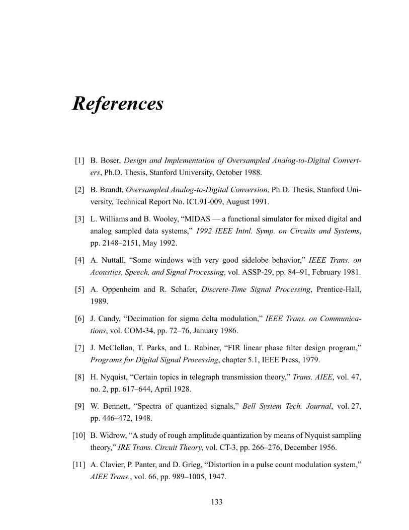
133
References
[1] B. Boser, Design and Implementation of Oversampled Analog-to-Digital Convert-
ers, Ph.D. Thesis, Stanford University, October 1988.
[2] B. Brandt, Oversampled Analog-to-Digital Conversion, Ph.D. Thesis, Stanford Uni-
versity, Technical Report No. ICL91-009, August 1991.
[3] L. Williams and B. Wooley, “MIDAS — a functional simulator for mixed digital and
analog sampled data systems,” 1992 IEEE Intnl. Symp. on Circuits and Systems,
pp. 2148–2151, May 1992.
[4] A. Nuttall, “Some windows with very good sidelobe behavior,” IEEE Trans. on
Acoustics, Speech, and Signal Processing, vol. ASSP-29, pp. 84–91, February 1981.
[5] A. Oppenheim and R. Schafer, Discrete-Time Signal Processing, Prentice-Hall,
1989.
[6] J. Candy, “Decimation for sigma delta modulation,” IEEE Trans. on Communica-
tions, vol. COM-34, pp. 72–76, January 1986.
[7] J. McClellan, T. Parks, and L. Rabiner, “FIR linear phase filter design program,”
Programs for Digital Signal Processing, chapter 5.1, IEEE Press, 1979.
[8] H. Nyquist, “Certain topics in telegraph transmission theory,” Trans. AIEE, vol. 47,
no. 2, pp. 617–644, April 1928.
[9] W. Bennett, “Spectra of quantized signals,” Bell System Tech. Journal, vol. 27,
pp. 446–472, 1948.
[10] B. Widrow, “A study of rough amplitude quantization by means of Nyquist sampling
theory,” IRE Trans. Circuit Theory, vol. CT-3, pp. 266–276, December 1956.
[11] A. Clavier, P. Panter, and D. Grieg, “Distortion in a pulse count modulation system,”
AIEE Trans., vol. 66, pp. 989–1005, 1947.
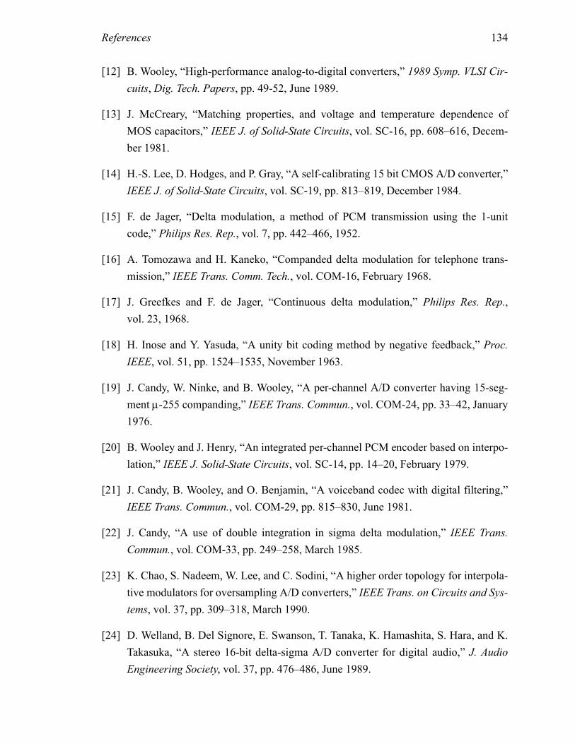
References 134
[12] B. Wooley, “High-performance analog-to-digital converters,” 1989 Symp. VLSI Cir-
cuits, Dig. Tech. Papers, pp. 49-52, June 1989.
[13] J. McCreary, “Matching properties, and voltage and temperature dependence of
MOS capacitors,” IEEE J. of Solid-State Circuits, vol. SC-16, pp. 608–616, Decem-
ber 1981.
[14] H.-S. Lee, D. Hodges, and P. Gray, “A self-calibrating 15 bit CMOS A/D converter,”
IEEE J. of Solid-State Circuits, vol. SC-19, pp. 813–819, December 1984.
[15] F. de Jager, “Delta modulation, a method of PCM transmission using the 1-unit
code,” Philips Res. Rep., vol. 7, pp. 442–466, 1952.
[16] A. Tomozawa and H. Kaneko, “Companded delta modulation for telephone trans-
mission,” IEEE Trans. Comm. Tech., vol. COM-16, February 1968.
[17] J. Greefkes and F. de Jager, “Continuous delta modulation,” Philips Res. Rep.,
vol. 23, 1968.
[18] H. Inose and Y. Yasuda, “A unity bit coding method by negative feedback,” Proc.
IEEE, vol. 51, pp. 1524–1535, November 1963.
[19] J. Candy, W. Ninke, and B. Wooley, “A per-channel A/D converter having 15-seg-
ment µ-255 companding,” IEEE Trans. Commun., vol. COM-24, pp. 33–42, January
1976.
[20] B. Wooley and J. Henry, “An integrated per-channel PCM encoder based on interpo-
lation,” IEEE J. Solid-State Circuits, vol. SC-14, pp. 14–20, February 1979.
[21] J. Candy, B. Wooley, and O. Benjamin, “A voiceband codec with digital filtering,”
IEEE Trans. Commun., vol. COM-29, pp. 815–830, June 1981.
[22] J. Candy, “A use of double integration in sigma delta modulation,” IEEE Trans.
Commun., vol. COM-33, pp. 249–258, March 1985.
[23] K. Chao, S. Nadeem, W. Lee, and C. Sodini, “A higher order topology for interpola-
tive modulators for oversampling A/D converters,” IEEE Trans. on Circuits and Sys-
tems, vol. 37, pp. 309–318, March 1990.
[24] D. Welland, B. Del Signore, E. Swanson, T. Tanaka, K. Hamashita, S. Hara, and K.
Takasuka, “A stereo 16-bit delta-sigma A/D converter for digital audio,” J. Audio
Engineering Society, vol. 37, pp. 476–486, June 1989.

References 135
[25] B. DelSignore, D. Kerth, N. Sooch, and E. Swanson, “A monolithic 20-b delta-
sigma A/D converter,” IEEE J. of Solid-State Circuits, vol. 25, pp. 1311–1317,
December 1990.
[26] E. Stikvoort, “Some remarks on the stability and performance of the noise shaper or
sigma-delta modulator,” IEEE Trans. on Communications, vol. 36, pp. 1157–1162,
October 1988.
[27] Y. Matsuya, K. Uchimura, A. Iwata, T. Kobayashi, M. Ishikawa, and T. Yoshitome,
“A 16-bit oversampling A-to-D conversion technology using triple-integration noise
shaping,” IEEE J. of Solid-State Circuits, vol. SC-22, pp. 921–929, December 1987.
[28] M. Rebeschini, N. van Bavel, P. Rakers, R. Greene, J. Caldwell, and J. Haug, “A
16-b 160-kHz CMOS A/D converter using sigma-delta modulation,” IEEE J. of
Solid-State Circuits, vol. 25, pp. 431-440, April 1990.
[29] L. Longo and M. Copeland, “A 13 bit ISDN-band oversampling ADC using two-
stage third order noise shaping,” IEEE 1988 Custom Integrated Circuits Conference,
pp. 21.2.1–4, 1988.
[30] L. Williams and B. Wooley, “Third-order cascaded sigma-delta modulators,” IEEE
Trans. on Circuits and Systems, vol. 38, pp. 489–498, May 1991.
[31] B. Boser and B. Wooley, “The design of sigma-delta modulation analog-to-digital
converters,” IEEE J. of Solid-State Circuits, vol. 23, pp. 1298–1308, December
1988.
[32] B. Brandt, D. Wingard, and B. Wooley, “Second-order sigma-delta modulation for
digital-audio signal acquisition,” IEEE J. of Solid-State Circuits, vol. 26, pp. 618–
627, April 1991.
[33] R. Gray, “Quantization noise spectra,” IEEE Trans. Information Theory, vol. 36,
pp. 1220–1244, November 1990.
[34] J. Candy and O. Benjamin, “The structure of quantization noise from sigma-delta
modulation,” IEEE Trans. on Communications, vol. COM-29, pp. 1316–1323, Sep-
tember 1981.
[35] B. Boser and B. Wooley, “Quantization error spectrum of sigma-delta modulators,”
1988 IEEE Intnl. Symp. on Circuits and Systems, pp. 2331–2334, 1988.
[36] J. Everard, “A single-channel PCM codec,” IEEE J. Solid-State Circuits, vol. SC-14,
pp. 25–37, February 1979.
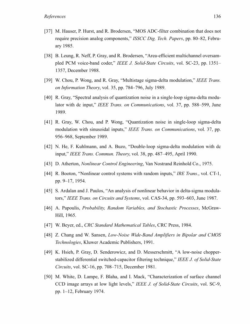
References 136
[37] M. Hauser, P. Hurst, and R. Brodersen, “MOS ADC-filter combination that does not
require precision analog components,” ISSCC Dig. Tech. Papers, pp. 80–82, Febru-
ary 1985.
[38] B. Leung, R. Neff, P. Gray, and R. Brodersen, “Area-efficient multichannel oversam-
pled PCM voice-band coder,” IEEE J. Solid-State Circuits, vol. SC-23, pp. 1351–
1357, December 1988.
[39] W. Chou, P. Wong, and R. Gray, “Multistage sigma-delta modulation,” IEEE Trans.
on Information Theory, vol. 35, pp. 784–796, July 1989.
[40] R. Gray, “Spectral analysis of quantization noise in a single-loop sigma-delta modu-
lator with dc input,” IEEE Trans. on Communications, vol. 37, pp. 588–599, June
1989.
[41] R. Gray, W. Chou, and P. Wong, “Quantization noise in single-loop sigma-delta
modulation with sinusoidal inputs,” IEEE Trans. on Communications, vol. 37, pp.
956–968, September 1989.
[42] N. He, F. Kuhlmann, and A. Buzo, “Double-loop sigma-delta modulation with dc
input,” IEEE Trans. Commun. Theory, vol. 38, pp. 487–495, April 1990.
[43] D. Atherton, Nonlinear Control Engineering, Van Nostrand Reinhold Co., 1975.
[44] R. Booton, “Nonlinear control systems with random inputs,” IRE Trans., vol. CT-1,
pp. 9–17, 1954.
[45] S. Ardalan and J. Paulos, “An analysis of nonlinear behavior in delta-sigma modula-
tors,” IEEE Trans. on Circuits and Systems, vol. CAS-34, pp. 593–603, June 1987.
[46] A. Papoulis, Probability, Random Variables, and Stochastic Processes, McGraw-
Hill, 1965.
[47] W. Beyer, ed., CRC Standard Mathematical Tables, CRC Press, 1984.
[48] Z. Chang and W. Sansen, Low-Noise Wide-Band Amplifiers in Bipolar and CMOS
Technologies, Kluwer Academic Publishers, 1991.
[49] K. Hsieh, P. Gray, D. Senderowicz, and D. Messerschmitt, “A low-noise chopper-
stabilized differential switched-capacitor filtering technique,” IEEE J. of Solid-State
Circuits, vol. SC-16, pp. 708–715, December 1981.
[50] M. White, D. Lampe, F. Blaha, and I. Mack, “Characterization of surface channel
CCD image arrays at low light levels,” IEEE J. of Solid-State Circuits, vol. SC-9,
pp. 1–12, February 1974.
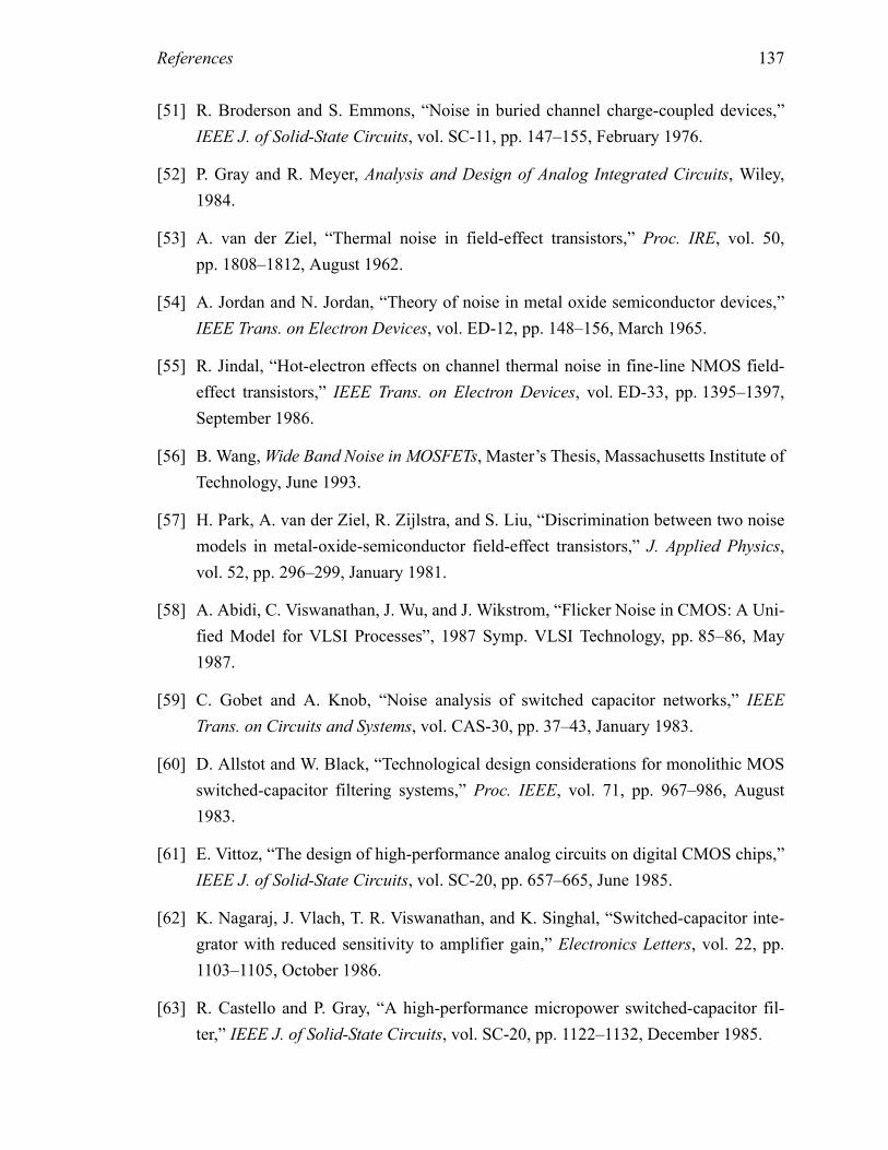
References 137
[51] R. Broderson and S. Emmons, “Noise in buried channel charge-coupled devices,”
IEEE J. of Solid-State Circuits, vol. SC-11, pp. 147–155, February 1976.
[52] P. Gray and R. Meyer, Analysis and Design of Analog Integrated Circuits, Wiley,
1984.
[53] A. van der Ziel, “Thermal noise in field-effect transistors,” Proc. IRE, vol. 50,
pp. 1808–1812, August 1962.
[54] A. Jordan and N. Jordan, “Theory of noise in metal oxide semiconductor devices,”
IEEE Trans. on Electron Devices, vol. ED-12, pp. 148–156, March 1965.
[55] R. Jindal, “Hot-electron effects on channel thermal noise in fine-line NMOS field-
effect transistors,” IEEE Trans. on Electron Devices, vol. ED-33, pp. 1395–1397,
September 1986.
[56] B. Wang, Wide Band Noise in MOSFETs, Master’s Thesis, Massachusetts Institute of
Technology, June 1993.
[57] H. Park, A. van der Ziel, R. Zijlstra, and S. Liu, “Discrimination between two noise
models in metal-oxide-semiconductor field-effect transistors,” J. Applied Physics,
vol. 52, pp. 296–299, January 1981.
[58] A. Abidi, C. Viswanathan, J. Wu, and J. Wikstrom, “Flicker Noise in CMOS: A Uni-
fied Model for VLSI Processes”, 1987 Symp. VLSI Technology, pp. 85–86, May
1987.
[59] C. Gobet and A. Knob, “Noise analysis of switched capacitor networks,” IEEE
Trans. on Circuits and Systems, vol. CAS-30, pp. 37–43, January 1983.
[60] D. Allstot and W. Black, “Technological design considerations for monolithic MOS
switched-capacitor filtering systems,” Proc. IEEE, vol. 71, pp. 967–986, August
1983.
[61] E. Vittoz, “The design of high-performance analog circuits on digital CMOS chips,”
IEEE J. of Solid-State Circuits, vol. SC-20, pp. 657–665, June 1985.
[62] K. Nagaraj, J. Vlach, T. R. Viswanathan, and K. Singhal, “Switched-capacitor inte-
grator with reduced sensitivity to amplifier gain,” Electronics Letters, vol. 22, pp.
1103–1105, October 1986.
[63] R. Castello and P. Gray, “A high-performance micropower switched-capacitor fil-
ter,” IEEE J. of Solid-State Circuits, vol. SC-20, pp. 1122–1132, December 1985.
References 138
[64] J. Fattaruso, S. Kiriaki, G. Warwar, M. de Wit, “Self-calibration techniques for a sec-
ond-order multibit sigma-delta modulator,” 1993 IEEE Intnl. Solid-State Circuits
Conf., pp. 228–229, February 1993.
[65] P. Gray and R. Meyer, “MOS operational amplifier design — a tutorial overview,”
IEEE J. of Solid-State Circuits, vol. SC-17, pp. 969–982, December 1982.
[66] T. Choi, R. Kaneshiro, R. Brodersen, P. Gray, W. Jett, and M. Wilcox, “High-fre-
quency CMOS switched-capacitor filters for communications application,” IEEE J.
Solid-State Circuits, vol. SC-18, pp. 652–664, December 1983.
[67] O. Feely and L. Chua, “The effect of integrator leak in Σ-∆ modulation,” IEEE
Trans. on Circuits and Systems, vol. 38, pp. 1293–1305, November 1991.
[68] C. Kaya, H. Tigelaar, J. Paterson, M. de Wit, J. Fattaruso, D. Hester, S. Kiriaki, K.
Tan, and F. Tsay, “Polycide/metal capacitors for high precision A/D converters,”
IEDM Tech. Digest, pp. 782–783, December 1988.
[69] K. Lee and R. Meyer, “Low-distortion switched-capacitor filter design techniques,”
IEEE J. of Solid-State Circuits, vol. SC-20, pp. 1103–1113, December 1985.
[70] A. Karanicolas, K. O, J. Wang, H.-S. Lee, and R. Reif, “A high-frequency fully dif-
ferential BiCMOS operational amplifier,” IEEE J. of Solid-State Circuits, vol. 26,
pp. 203–208, March 1991.
[71] B. Brandt and B. Wooley, “A 50-MHz multibit sigma-delta modulator for 12-b 2-
MHz A/D conversion,” IEEE J. of Solid-State Circuits, vol. 26, pp. 1746–1756,
December 1991.
[72] Panasonic VP-7214A RC Oscillator Instruction Manual, Matsushita Communica-
tion Industrial Co., Ltd., Yokohama, Japan.
[73] D. Su, M. Loinaz, S. Masui, and B. Wooley, “Experimental results and modeling
techniques for substrate noise in mixed-signal integrated circuits,” IEEE J. of Solid-
State Circuits, vol. 28, pp. 420–430, April 1993.
[74] S. Norsworthy, I. Post, and H. Fetterman, “A 14-bit 80-kHz sigma-delta A/D con-
verter: Modeling, design, and performance evaluation,” IEEE J. of Solid-State Cir-
cuits, vol. 24, pp. 256–266, April 1989.