j-std-001f feb 2012 - · pdf file1.1 scope this standard prescribes practices and requirements...
TRANSCRIPT

J-STD-001 Revision F Draft for February 2012
©Copyright IPC, copying permitted only for use in developing J-STD-001 Revision F. 1
J-STD-001F
Requirements for Soldered Electrical and Electronic Assemblies
Working Draft February 2012

J-STD-001 Revision F Draft for February 2012
©Copyright IPC, copying permitted only for use in developing J-STD-001 Revision F. 2
1 GENERAL 1.1 Scope This standard prescribes practices and requirements for the manufacture of soldered electrical and electronic assemblies. Historically, electronic assembly (soldering) standards contained a more comprehensive tutorial addressing principles and techniques. For a more complete understanding of this document’s recommendations and requirements, one may use this document in conjunction with IPC-HDBK-001 and IPC-A-610. 1.2 Purpose This standard describes materials, methods and acceptance criteria for producing soldered electrical and electronic assemblies. The intent of this document is to rely on process control methodology to ensure consistent quality levels during the manufacture of products. It is not the intent of this standard to exclude any procedure for component placement or for applying flux and solder used to make the electrical connection. 1.3 Classification This standard recognizes that electrical and electronic assemblies are subject to classifications by intended end-item use. Three general end-product classes have been established to reflect differences in producibility, complexity, functional performance requirements, and verification (inspection/test) frequency. It should be recognized that there may be overlaps of equipment between classes. The user (see 1.8.13) is responsible for defining the product class. The product class should be stated in the procurement documentation package. CLASS 1 General Electronic Products Includes products suitable for applications where the major requirement is function of the completed assembly. CLASS 2 Dedicated Service Electronic Products Includes products where continued performance and extended life is required, and for which uninterrupted service is desired but not critical. Typically the end-use environment would not cause failures. CLASS 3 High Performance Electronic Products Includes products where continued high performance or performance-on-demand is critical, equipment downtime cannot be tolerated, end-use environment may be uncommonly harsh, and the equipment must function when required, such as life support or other critical systems. 1.4 Measurement Units and Applications All dimensions and tolerances, as well as other forms of measurement (temperature, weight, etc.) in this standard are expressed in SI (System International) units (with Imperial English equivalent dimensions provided in brackets). Dimensions and tolerances use millimeters as the main form of dimensional expression; micrometers are used when the precision required makes millimeters too cumbersome. Celsius is used to express temperature. Weight is expressed in grams. 1.4.1 Verification of Dimensions Actual measurement of specific part mounting and solder fillet dimensions and determination of percentages are not required except for referee purposes. For the purposes of determining conformance to this specification, all specified limits in this standard are absolute limits as defined in ASTM E29. 1.5 Definition of Requirements The word shall is used in the text of this document wherever there is a requirement for materials, preparation, process control or acceptance of a soldered connection. Where the word shall is used in this Standard, the requirements for each class are in brackets next to the shall requirement. N = No requirement has been established for this Class A = Acceptable P = Process Indicator D = Defect Examples: [A1P2D3] is Acceptable Class 1, Process Indicator Class 2 and Defect Class 3 [N1D2D3] is Requirement Not Establish Class 1, Defect Classes 2 and 3 [A1A2D3] is Acceptable Classes 1 and 2, Defect Class 3 [D1D2D3] is Defect for all Classes.

J-STD-001 Revision F Draft for February 2012
©Copyright IPC, copying permitted only for use in developing J-STD-001 Revision F. 3
A defect for a Class 1 product means that the characteristic is also a defect for Class 2 and 3. A defect for a Class 2 product means that the characteristic is also a defect for a Class 3 product, but may not be a defect for a Class 1 product where less demanding criteria may apply. The word “should” reflects recommendations and is used to reflect general industry practices and procedures for guidance only. Line drawings and illustrations are depicted herein to assist in the interpretation of the written requirements of this standard. Text takes precedence over the figures. IPC-HDBK-001, a companion document to this specification, contains valuable explanatory and tutorial information compiled by IPC Technical Committees that is relative to this specification. Although the Handbook is not a part of this specification, when there is confusion over the specification verbiage, the reader is referred to the Handbook for assistance. When the space shuttle symbol appears next to a paragraph it indicates that J-STD-001ES Space Applications Electronic Hardware Addendum to J-STD-001E contains different requirements to this paragraph. The criteria in J-STD-001ES are not applicable unless the addendum is specifically required by procurement documentation. 1.5.1 Hardware Defects and Process Indicators Hardware characteristics or conditions that do not conform to the requirements of this specification are classified as either hardware defects or hardware process indicators. A defect is a condition that may affect the form, fit, or function of the item in its end use environment, or other risk factors as identified by the manufacturer (see 1.8.5). Defects shall [D1D2D3] be identified, documented, and dispositioned by the manufacturer based on the design, service, and customer requirements. Disposition is the determination of how defects are to be treated, and include, but are not limited to, rework, scrap, use as-is, or repair. A process indicator is a condition (not a defect) that is attributable to variation in material, equipment operation, workmanship or processes, but that does not affect the form, fit, or function of a product. Not all process indicators specified by this standard are noted. Hardware process indicator data should be monitored (see 11.3), but the hardware need not be dispositioned. It is the responsibility of the user (see 1.8.13) to define additional defect categories applicable to the product. It is the responsibility of the manufacturer (see 1.8.5) to identify defects and process indicators that are unique to the assembly process (see 1.13.2). 1.5.2 Material and Process Nonconformance Hardware found to be produced using either materials or processes that do not conform to the requirements of this standard shall [D1D2D3] be dispositioned when the condition is a defect. This disposition shall [D1D2D3] address the potential effect of the nonconformance on functional capability of the hardware such as reliability and design life (longevity). Note: Material and process nonconformance differs from hardware defects or hardware process indicators in that the material/process nonconformance often does not result in an obvious change in the hardware’s appearance but can impact the hardware’s performance; e.g., contaminated solder, incorrect solder alloy (per drawing/procedure). 1.6 General Requirements When this standard is used, the user and manufacturer shall [D1D2D3] agree on the class to which the product belongs.” If the user and manufacturer do not establish and document the acceptance class, the manufacturer may do so. The soldering operations, equipment, and conditions described in this document are based on electrical/ electronic circuits designed and fabricated in accordance with the specifications listed in Table 1-1. Table 1-1 Design, Fabrication and Acceptability Specification
Board Type Design Specification Fabrication Specification Generic Requirements IPC-2221 IPC-6011
Rigid Printed Boards IPC-2222 IPC-6012
IPC-A-600 Flexible Circuits IPC-2223 IPC-6013 Rigid Flex Board IPC-2223 IPC-6013
1.7 Order of Precedence The contract shall [D1D2D3] take precedence over this standard, referenced standards and drawings.
J-STD-001 Revision F Draft for February 2012
©Copyright IPC, copying permitted only for use in developing J-STD-001 Revision F. 4
1.7.1 Conflict In the event of conflict between the requirements of this standard and the applicable assembly drawing(s)/ documentation, the applicable user approved assembly drawing(s)/documentation govern. In the event of a conflict between the text of this standard and the applicable documents cited herein, the text of this standard takes precedence. In the event of conflict between the requirements of this standard and an assembly drawing(s)/documentation that has not been user approved, this standard governs. When IPC J-STD-001 is cited or required by contract, the requirements of IPC-A-610 do not apply unless separately or specifically required. When IPC-A-610 or other related documents are cited along with IPC J-STD-001 the order of precedence shall (D1D2D3) be defined in the procurement documents. Note: When IPC-A-610 is used as a companion document to J-STD-001, the revisions of J-STD-001 and IPC-A-610 should correspond, e.g., J-STD-001D and IPC-A-610D. The likelihood of criteria not aligning increases when different revisions are used together. The user (customer) has the responsibility to specify acceptance criteria. If no criteria is specified, required, or cited, then best manufacturing practice applies. 1.7.2 Clause References When a clause in this document is referenced, its subordinate clauses also apply. 1.7.3 Appendices Appendices to this Standard are not binding requirements unless separately and specifically required by the applicable contracts, assembly drawing(s), documentation or purchase orders. 1.8 Terms and Definitions Other than those terms listed below, the definitions of terms used in this standard are in accordance with IPC-T-50. 1.8.1 Defect A nonconformance to the requirements of this standard or other risk factors as identified by the manufacturer (see 1.8.5). 1.8.2 Disposition The determination of how defects should be treated. Dispositions include, but are not limited to, rework, use as is, scrap or repair. 1.8.3 Electrical Clearance The minimum spacing between noncommon uninsulated conductors (e.g., patterns, materials, hardware, residue) is referred to as “minimum electrical clearance” throughout this document and is defined in the applicable design standard or on the approved or controlled documentation. Insulating material needs to provide sufficient electrical isolation. In the absence of a known design standard use Appendix B (derived from IPC-2221). 1.8.4 High Voltage The term “high voltage” will vary by design and application. The high voltage criteria in this document are only applicable when specifically required in the drawings/procurement documentation. 1.8.5 Manufacturer (Assembler) The individual, organization, or company responsible for the assembly process and verification operations necessary to ensure full compliance of assemblies to this standard. 1.8.6 Objective Evidence Documentation in the form of hard copy, computer data, video, or other media. 1.8.7 Process Control A system or method to continually steer an operation in reducing variation in the processes or products to meet or exceed the goal in quality and performance. 1.8.8 Process Indicator A detectable anomaly, other than a defect, that is attributable to variation in material, equipment operation, workmanship or processes. 1.8.9 Proficiency The capability to perform tasks in accordance with the requirements and verification procedures detailed in this standard. 1.8.10 Solder Destination Side The solder destination side is that side of the printed circuit board (PCB) that the solder flows toward in a plated-through hole application. 1.8.11 Solder Source Side The solder source side is the side of the PCB to which solder is applied. 1.8.12 Supplier The individual, organization or company which provides the manufacturer (assembler) components (electronic, electromechanical, mechanical, printed boards, etc.) and/or materials (solder, flux, cleaning agents, etc.).

J-STD-001 Revision F Draft for February 2012
©Copyright IPC, copying permitted only for use in developing J-STD-001 Revision F. 5
1.8.13 User The individual, organization, company, contractually designated authority, or agency responsible for the procurement of electrical/electronic hardware, and having the authority to define the class of equipment and any variation or restrictions to the requirements of this standard (i.e., the originator/custodian of the contract detailing these requirements). 1.8 .14 Wire Overwrap Wire overwrap occurs when a wire/lead is wrapped more than 360° and remains in contact with the terminal post, see Figure 1-1. 1.8.15 Wire Overlap Wire overlap occurs when a wire/lead is wrapped more than 360° and crosses over itself, i.e., does not remain in contact with the terminal post, see Figure 1-2. Figure 1-1 Overwrap Figure 1-2 Overlap 1.9 Requirements Flowdown When this standard is contractually required, the applicable requirements of this standard (including product class - see 1.3) shall [D1D2D3] be imposed on all applicable subcontracts, assembly drawing(s), documentation and purchase orders. Unless otherwise specified the requirements of this standard are not imposed on the procurement of commercial-off-the-shelf (COTS or catalog) assemblies or subassemblies. When a part is adequately defined by a specification, then the requirements of this standard should be imposed on the manufacture of that part only when necessary to meet end-item requirements. When it is unclear where flowdown should stop, it is the responsibility of the manufacturer to establish that determination with the user. When an assembly (i.e., daughterboard,) is procured that assembly should meet the requirements of this standard. If the assembly is manufactured by the same manufacturer, the solder requirements are as stated in the contract for the entire assembly. 1.10 Personnel Proficiency All instructors, operators, and inspection personnel shall [N1D2D3] be proficient in the tasks to be performed. Objective evidence of that proficiency shall [N1D2D3] be maintained and be available for review. Objective evidence should include records of training to the applicable job functions being performed, work experience, testing to the requirements of this standard, and/or results of periodic reviews of proficiency. Supervised on-the-job training is acceptable until proficiency is demonstrated. 1.11 Acceptance Requirements All products shall [D1D2D3] meet the requirements of the assembly drawing(s)/ documentation and the requirements for the applicable product class specified herein. Manufacturers shall [N1D2D3] perform 100% inspection unless sampling inspection is defined as part of a documented process control plan (see 11.2.2). 1.12 General Assembly Requirements The electrical and mechanical integrity of components and assemblies shall [D1D2D3] be retained after exposure to processes employed during manufacture and assembly (e.g., handling, baking, fluxing, soldering, and cleaning). 1.13 Miscellaneous Requirements 1.13.1 Health and Safety The use of some materials referenced in this standard may be hazardous. To provide for personnel safety, follow the applicable local and Federal (National) occupational, safety and health regulations. 1.13.2 Procedures for Specialized Technologies As an industry consensus standard, this document cannot address all of the possible components and product design combinations, e.g., magnetic windings, high frequency, high voltage, etc. Where uncommon or specialized technologies are used, it may be necessary to develop unique process and/or acceptance criteria. Often, unique definition is necessary to consider the specialized characteristics while considering product performance criteria. The development should include user involvement. The acceptance criteria shall [N1N2D3] have user agreement. Mounting and soldering requirements for specialized processes and/or technologies not specified herein shall [N1D2D3] be performed in accordance with documented procedures which are available for review. Whenever possible these criteria should be submitted to the IPC Technical Committee to be considered for inclusion in upcoming revisions of this standard.

J-STD-001 Revision F Draft for February 2012
©Copyright IPC, copying permitted only for use in developing J-STD-001 Revision F. 6
1.13.2.1 Manufacture of Devices Incorporating Magnetic Windings This standard is very limited in its applicability to the manufacturing processes associated with the mounting of internal electronic elements and the soldering of the internal connections of transformers, motors, and similar devices. Unless a user has a specific need for the controls provided by this standard, it should not be imposed relative to the manufacture of the internal elements of these devices. The external interconnect points (e.g., terminals, pins, etc.) shall [D1D2D3] meet the solderability requirements of 4.3. 1.13.2.2 High Frequency Applications High frequency applications (i.e., radio wave and microwaves) may require part clearances, mounting systems, and assembly designs which vary from the requirements stated herein. 1.13.2.3 High Voltage Applications High voltage applications may require part clearances, mounting systems, and assembly designs which vary from the requirements stated herein. There shall [D1D2D3] be no broken strands for wires used at a potential of 6 kV or greater. 2 APPLICABLE DOCUMENTS <UPDATE AT PUBLICATION> The following documents, of the issue in effect on the invitation for bid, form a part of this specification to the extent specified herein. 2.1 EIA1 EIA-557-1 Statistical Process Control Guidance for Selection of Critical Manufacturing Operations for Use Implementing an SPC System for Passive Components 2.2 IPC2 HDBK-001 Requirements for Soldered Electrical Electronic Assemblies Handbook IPC-T-50 Terms and Definitions for Interconnecting and Packaging Electronic Circuits IPC-D-279 Design Guidelines for Reliable Surface Mount Technology Printed Board Assemblies IPC-A-600 Acceptability of Printed Boards IPC-A-610 Acceptability of Electronic Assemblies IPC-OI-645 Standard for Visual Optical Inspection Aids IPC-SM-785 Guidelines for Accelerated Reliability Testing of Surface Mount Attachments IPC-TM-650 Test Methods Manual3 2.3.25 Detection and Measurement of Ionizable Surface Contaminants 2.3.27 Cleanliness Test Residual Rosin 2.3.39 Surface Organic Contamination Identification Test (Infrared Analytical Method) 2.4.22 Bow and Twist 2.6.9.1 Test to Determine Sensitivity of Electronic Assemblies to Ultrasonic Energy and Test Method 2.6.9.2 Test to Determine Sensitivity of Electronic Components to Ultrasonic Energy 2.6.23 Conductive Anodic Filament (CAF) Resistance Test: X-Y Axis IPC-SM-817 General Requirements for Dielectric Surface Mounting Adhesives IPC-CC-830 Qualification and Performance of Electrical Insulating Compound for Printed Board Assemblies IPC-2221 Generic Standard on PWB Design IPC-2222 Sectional Standard on Rigid PWB Design IPC-2223 Sectional Design Standard for Flexible Printed Boards IPC-6011 Generic Performance Specification of Printed Boards IPC-6012 Qualification and Performance Specification for Rigid Printed Boards IPC-6013 Qualification and Performance for Flexible Printed Boards IPC-7095 Design and Assembly Process Implementation for BGAs IPC-7530 Guidelines for Temperature Profiling for Mass Soldering Processes (Reflow & Wave) IPC-9191 General Guidelines for Implementation of Statistical Process Control (SPC) IPC-9201 Surface Insulation Resistance Handbook IPC-9261 In-Process DPMO and Estimated Yield for PWAs IPC-9691 User Guide for the IPC-TM-650, Method 2.6.25, Conductive Anodic Filament (CAF) Resistance Test (Electrochemical Migration Testing) IPC-9701 Performance Test Methods and Qualification Requirements for Surface Mount Solder Attachments 2.3 Joint Industry Standards4 IPC/EIA J-STD-002 Solderability Tests for Component Leads, Terminations, Lugs, Terminals and Wires

J-STD-001 Revision F Draft for February 2012
©Copyright IPC, copying permitted only for use in developing J-STD-001 Revision F. 7
J-STD-003 Solderability Tests for Printed Boards J-STD-004 Requirements for Soldering Fluxes J-STD-005 Requirements for Soldering Paste J-STD-006 Requirements for Electronic Grade Solder Alloys and Fluxed and Non-Fluxed Solid Solders for Electronic Soldering Applications IPC/JEDEC J-STD-020 Moisture/Reflow Sensitivity Classification for Plastic Integrated Circuit Surface Mount Devices IPC/JEDEC J-STD-033 Standard for Handling, Packing, Shipping and Use of Moisture/Reflow Sensitive Surface Mount Devices IPC/JEDEC J-STD-075 Classification of Non-IC Electronic Components for Assembly Processes IPC/JEDEC-9701 Performance Test Methods and Qualification Requirements for Surface Mount Solder Attachments 2.4 ASTM5 ASTM E29 Standard Practice for Using Significant Digits in Test Data to Determine Conformance with Specifications 2.5 Electrostatic Discharge Association6 ANSI/ESD-S-20.20 Protection of Electrical and Electronic Parts, Assemblies and Equipment 3 MATERIALS, COMPONENTS AND EQUIPMENT REQUIREMENTS 3.1 Materials The materials and processes used to assemble/manufacture electronic assemblies shall [D1D2D3] be selected such that their use, in combination, produce products acceptable to this standard. When major elements of the proven processes are changed, (e.g., flux, solder paste, cleaning media or system, solder alloy or soldering system) validation of the acceptability of the change(s) shall [N1N2D3] be performed and documented. They can also pertain to a change in bare boards, solder resist or metallization. 3.2 Solder Solder alloys shall [D1D2D3] be in accordance with J-STD-006 or equivalent. Solder alloys other than Sn60Pb40, Sn62Pb36Ag2, and Sn63Pb37 that provide the required electrical and mechanical attributes may be used if all other conditions of this standard are met and objective evidence of such is available for review. Flux that is part of flux-cored solder wire shall [D1D2D3] meet the requirements of 3.3. Flux percentage is optional. 3.2.1 Solder - Lead Free Solder alloys less than 0.1% lead by weight not listed by J-STD-006 may be used when such use is agreed upon by the manufacturer and the user. 3.2.2 Solder Purity Maintenance Solder used for preconditioning, gold removal, tinning of parts, and machine soldering shall [N1D2D3] be analyzed, replaced or replenished at a frequency to ensure compliance with the limits specified in Table 3-1. Solder alloys other than Sn60Pb40, Sn62Pb36Ag2, or Sn63Pb37 tin/lead solders shall [N1D2D3] be in compliance with equivalent documented limits. If contamination exceeds the limits, intervals between the analyses, replacement or replenishment shall [N1D2D3] be shortened. The frequency of analysis should be determined on the basis of historical data, or monthly analyses. Records containing the results of all analyses and solder bath usage (e.g., total time in use, amount of replacement solder, or area throughput) shall [N1D2D3] be maintained for a minimum of one year for each process/ system. SnPb alloys used for preconditioning or assembly shall [N1D2D3] have a tin content maintained within ± 1.5% of the nominal alloy being used. Tin content for SnPb alloys shall [N1D2D3] be tested at the same frequency as testing for copper/gold contamination. The balance of the SnPb bath shall [N1D2D3] be lead and/or the items listed in Table 3-1. Lead-free alloys used for preconditioning or assembly shall [N1D2D3] have a tin content maintained within ± 1% of the nominal alloy being used. Tin content for lead-free alloys shall [N1D2D3] be tested at the same frequency as testing for copper/silver contamination. The balance of the lead-free bath shall [N1D2D3] be the items listed in Table 3-1.
J-STD-001 Revision F Draft for February 2012
©Copyright IPC, copying permitted only for use in developing J-STD-001 Revision F. 8
Table 3-1 Maximum Limits of Solder Bath Contaminant
Contaminant
Preconditioning Maximum Contaminant Weight
Percentage Limit SnPb Alloys
Assembly Maximum Contaminant Weight
Percentage Limit SnPb Alloys
Preconditioning and Assembly Maximum Contaminant Weight Percentage Limit
Lead-free Alloys1 Copper 0.75 0.3 1.13 Gold 0.5 0.2 0.2
Cadmium 0.01 0.005 0.005 Zinc 0.008 0.005 0.005
Aluminum 0.008 0.006 0.006 Antimony 0.5 0.5 0.2
Iron 0.02 0.02 0.02 Arsenic 0.03 0.03 0.03 Bismuth 0.25 0.25 0.25 Silver2 0.75 0.1 4.0 Nickel 0.025 0.01 0.05 Lead N/A N/A 0.1
Total of Copper, Gold, Cadmium, Zinc,
Aluminum Contaminates N/A 0.4 N/A
Note 1: Maximum contamination limits are applicable for Sn96.5Ag3.0Cu0.5 (SAC305) per J-STD-006. Other Lead-free solder alloy contamination limits may be used upon agreement between user and vendor.
Note 2: Not applicable for Pb36B: limits to be 1.75% to 2.25%. Note 3: A maximum copper limit of 1.0% may be specified as agreed between user and supplier. Printed circuit assemblies that are
characterized as thick and thermally demanding may have potential plated through hole fill and/or solder joint defects due to the impact of copper on solder flow characteristics.
3.3 Flux Flux shall [D1D2D3] be in accordance with J-STD-004 or equivalent. Flux shall [N1N2D3] conform to flux activity levels L0 and L1 of flux materials rosin (RO), resin (RE), or organic (OR), except ORL1 shall not [N1N2D3] be used for no-clean soldering. When other activity levels or flux materials are used, data demonstrating compatibility shall [N1N2D3] be available for review (see 3.1). Note: Flux or solder paste soldering process combinations previously tested or qualified in accordance with other specifications do not require additional testing. Type H or M fluxes shall not [D1D2D3] be used for tinning or attachment of stranded wires. 3.3.1 Flux Application When an external flux is used in conjunction with flux cored solders, the fluxes shall [D1D2D3] be compatible. 3.4 Solder Paste Solder paste shall [D1D2D3] be in accordance with J-STD-005 or equivalent. Solder paste shall [D1D2D3] also meet the requirements of 3.2 and 3.3. 3.5 Solder Preforms Solder preforms shall [D1D2D3] meet the requirements of 3.2 and 3.3. 3.6 Adhesives Electrically nonconductive adhesive materials used for attachment of components should conform to an acceptable document or standard, e.g., IPC-SM-817, or as otherwise specified. The adhesives selected shall not [D1D2D3] be detrimental to the component or assembly they are used on. The material shall [D1D2D3] be cured. 3.7 Chemical Strippers Chemical solutions, pastes, and creams shall not [D1D2D3] cause damage or degradation. 3.8 Components Components (e.g., electronic devices, mechanical parts, printed boards) selected for assembly shall [D1D2D3] be compatible with all materials and processes, e.g., temperature ratings, used to manufacture the assembly/ product. Moisture or process sensitive components (as classified by IPC/JEDEC J-STD-020, ECA/IPC/JEDEC J-STD-075 or other documented classification procedure) shall [D1D2D3] be handled in a manner consistent with IPC/JEDEC J-STD-033 or other documented procedure.

J-STD-001 Revision F Draft for February 2012
©Copyright IPC, copying permitted only for use in developing J-STD-001 Revision F. 9
3.8.1 Component and Seal Damage Components and lead seals shall not [D1D2D3] be degraded below the part specification requirements. Minor surface flaws, discoloration, meniscus cracks, or chips in component bodies are acceptable. However, they shall not [D1D2D3] expose the component substrate or active element nor affect structural integrity. Components shall not [D1D2D3] be charred. Note: Visual aids can be found in IPC-A-610. 3.8.2 Coating Meniscus Component coating meniscus shall not [N1D2D3] be trimmed. 3.9 Soldering Tools and Equipment Tools and equipment shall [D1D2D3] be selected, used and maintained such that no damage or degradation that would be detrimental to the designed function of parts or assemblies would result from their use. Soldering irons, equipment, and systems shall [D1D2D3] be chosen and employed to provide temperature control and isolation from electrical overstress or ESD (see 4.1). A tool used to cut leads shall not [D1D2D3] impart shock that damages a component lead seal or internal connection. See Appendix A for guidelines on tool selection and maintenance. 4 GENERAL SOLDERING AND ASSEMBLY REQUIREMENTS 4.1 Electrostatic Discharge (ESD) If any ESD susceptible devices are employed, the manufacturer shall [D1D2D3] establish and implement a documented ESD control program in accordance with ANSI/ESD-S-20.20 or as otherwise specified. Documentation necessary for an effective program shall [D1D2D3] be available for review. 4.2 Facilities Cleanliness and ambient environments in all work areas shall [D1D2D3] be maintained at levels that prevent contamination or deterioration of soldering tools, materials, and surfaces to be soldered. Eating, drinking, and/or use of tobacco products shall [D1D2D3] be prohibited in the work area. 4.2.1 Environmental Controls The soldering facility should be enclosed, temperature and humidity controlled, and maintained at a positive pressure. 4.2.2 Temperature and Humidity When humidity decreases to a level of 30% or lower, the manufacturer shall [N1D2D3] verify that electrostatic discharge control is adequate, and that the range of humidity in the assembly area is sufficient to allow soldering and assembly materials to function correctly in the process, based on vendor recommendations or documented evidence of process performance. For operator comfort and solderability maintenance, the temperature should be maintained between 18°C [64.4°F] and 30°C [86°F] and the relative humidity should not exceed 70%. For process control, more restrictive temperature and humidity limits may be required. 4.2.3 Lighting Illumination at the surface of workstations should be at least 1000 lm/m2 (approximately 93 foot candles). Supplemental lighting may be necessary to assist in visual inspection. Light sources should be selected to prevent shadows on the item being inspected except those caused by the item being inspected. Note: In selecting a light source, the color temperature of the light is an important consideration. Light ranges from 3000- 5000° K enable users to distinguish various printed circuit assembly features and contaminates with increased clarity. 4.2.4 Field Assembly Operations In field assembly operations on Class 3 products where the controlled environmental conditions required by this standard cannot be effectively achieved, precautions shall [N1N2D3] be taken to maximize the quality of solder connections and minimize the effects of the uncontrolled environment on the operation being performed on the hardware. 4.3 Solderability Electronic/mechanical components (including PCBs) and wires to be soldered shall [D1D2D3] meet the solderability requirements of J-STD-002 or equivalent and printed boards shall [D1D2D3] meet the requirements of J-STD003 or equivalent. When a solderability inspection operation or pretinning and inspection operation is performed as part of the documented assembly process, that operation may be used in lieu of solderability testing (see 4.4). 4.4 Solderability Maintenance The manufacturer shall [D1D2D3] ensure that all components, parts, leads, wiring, terminals, and printed boards that have met the requirements of 4.3 are solderable at the start of hand and/or machine soldering operations. The manufacturer should establish procedures to minimize part solderability degradation (see IPC-HDBK-001). 4.5 Removal of Component Surface Finishes Certain surface finishes on component terminations or PCB lands may impact the quality of the solder connection. Follow the requirements of 4.5.1 and 4.5.2.

J-STD-001 Revision F Draft for February 2012
©Copyright IPC, copying permitted only for use in developing J-STD-001 Revision F. 10
The following requirements may be eliminated: a. If there is documented objective evidence, available for review, that there are no gold related solder embrittlement issues, or
other metallic surface finish solder joint integrity problems (e.g., with Sn or SnBi) associated with the soldering process being used (see IPC-HDBK-001 or IPC-AJ-820 handbook for guidance).
b. For electroless nickel immersion gold (ENIG), nickel-palladium-gold (NiPdAu), or electroless nickel electroless palladium immersion gold (ENEPIG) finishes.
4.5.1 Gold Removal Gold shall [N1P2D3] be removed: a. From at least 95% of the surfaces to be soldered of the through-hole component leads with >2.54 µm [100 µin] or more of gold
thickness. <Sep2011> b. From 95% of all surfaces to be soldered of surface mount components regardless of gold thickness. c. From the surfaces to be soldered of solder terminals plated with >2.54 µm [100 µin] or more of gold thickness. <Sep2011>
A double tinning process or dynamic solder wave may be used for gold removal prior to mounting the component on the assembly. 4.5.2 Other Metallic Surface Finishes Removal Other metallic surface finishes shall [N1P2D3] be removed from 95% of the surfaces to be soldered on components if it is determined that the solder joint integrity will be compromised. 4.6 Thermal Protection When hand soldering, tinning or reworking a component identified as heat sensitive, protective measures shall [D1D2D3] be taken to minimize component heating or prevent thermal shock, e.g., heat sink, thermal shunt, preheat. Protection may be provided through a controlled heating process. 4.7 Rework of Nonsolderable Parts A component lead, termination, or board not conforming to the solderability requirements of 4.3 may be reworked (e.g., by dipping in hot solder) before soldering. A reworked part shall [D1D2D3] conform to the requirements of 4.3, less steam conditioning. 4.8 Presoldering Cleanliness Requirements The assembly shall [D1D2D3] be clean of any matter that will inhibit compliance to the requirements of this standard. 4.9 General Part Mounting Requirements When design restrictions mandate mounting components incapable of withstanding soldering temperatures incident to a particular process, such components shall [D1D2D3] be mounted and soldered to the assembly as a separate operation. If cleaning is required, parts shall [D1D2D3] be mounted with sufficient clearances between the body and the PCB to assure adequate cleaning and cleanliness testing. Assemblies should be cleaned after each soldering operation so that subsequent placement and soldering operations are not impaired by contamination (see 8, Cleaning Process Requirements). Parts should be mounted such that part markings and reference designators are visible (see 9.2). Any violation of minimum electrical clearance as a result of nonconformance to defined criteria is a defect condition. 4.9.1 Stress Relief At least one component lead shall [D1D2D3] have stress relief (see Figure 5-7) provided the component is not clip or adhesive mounted, or otherwise constrained. All leads shall [D1D2D3] have stress relief when the component is clip or adhesive mounted or otherwise constrained. Wires connected to terminals shall [A1P2D3] have stress relief. 4.9.2 General Requirements Unless otherwise defined, the requirements for mounting apply to both wires and component leads (see 5.1). 4.9.3 Lead Deformation Limits Leads shall not [D1D2D3] have nicks or deformation exceeding 10% of the diameter, width, or thickness of the lead except as allowed for flattened leads (see 7.1.4). 4.10 Hole Obstruction Parts and components shall [A1P2D3] be mounted such that they do not obstruct solder flow onto the solder destination side lands of plated through holes (PTHs) required to be soldered (see Figure 4-1 and 4.18.3).

J-STD-001 Revision F Draft for February 2012
©Copyright IPC, copying permitted only for use in developing J-STD-001 Revision F. 11
Figure 4-1 Hole Obstruction 1. Hard mount 2. Air 3. Component body 4. Solder 4.11 Metal-Cased Component Isolation Metal-cased components shall [D1D2D3] be isolated from adjacent electrically conductive elements. 4.12 Adhesive Coverage Limits Adhesive materials, when used, shall not [D1D2D3] preclude the formation of an acceptable solder connection. Adhesive materials extending from under SMT components shall not [A1P2D3] be visible in the termination area. Adhesives, e.g., staking, bonding, shall not [D1D2D3] contact an unsleeved area of a sleeved glass body component. 4.13 Mounting of Parts on Parts (Stacking of Components) When part stacking is permitted by the assembly drawing(s)/ documentation, parts shall not [D1D2D3] violate minimum electrical clearance between other parts or components. 4.14 Connectors and Contact Areas The mating surface(s) of connectors or contact areas intended for electrical connection shall [D1D2D3] be free of contaminants or foreign material. 4.15 Handling of Parts Parts shall [D1D2D3] be handled in a manner to preclude damage to terminations and to avoid the need for subsequent lead straightening operations. Once parts are mounted on printed boards, the unsoldered assembly shall [D1D2D3] be handled, transported (e.g., hand or conveyor) and processed in a manner to preclude movement that would detrimentally affect formation of acceptable solder connections. When parts are mounted in solder paste, the unsoldered assembly should be processed so that the part does not move within the solder paste such that the final soldered connection results in part misalignment exceeding the requirements of Section 7. After soldering operations have been performed, the assembly shall [D1D2D3] be sufficiently cooled so the solder is solidified prior to further handling. 4.15.1 Preheating For other than hand soldering, assemblies should be preheated to minimize the presence of volatile solvents prior to exposure to molten solder to reduce thermal shock to boards and components, to improve solder flow, and to reduce the solder dwell time. The preheat temperature exposure shall not [D1D2D3] degrade printed boards, components, or soldering performance. 4.15.2 Controlled Cooling Controlled cooling may be used. If used, controlled (accelerated or slowed ramp) cooling shall [N1D2D3] be in accordance with documented procedures. 4.15.3 Drying/Degassing Prior to soldering, the assembly may be treated to reduce detrimental moisture and other volatiles. 4.15.4 Holding Devices and Materials Equipment, devices, materials, or techniques used to handle boards or retain parts and components to the printed boards through any and all stages of soldering shall not [D1D2D3] contaminate, damage, or degrade printed boards or components. The equipment, devices, materials or techniques should be adequate to maintain component positioning and permit solder flow through plated-through holes and/or onto terminal areas. 4.16 Machine (Nonreflow) Soldering 4.16.1 Machine Controls The manufacturer shall [N1D2D3] maintain operating procedures describing the soldering process and the proper operation of the automatic soldering machine and associated equipment. For the soldering machine, these procedures, as a minimum, shall [N1D2D3] define the preheat temperature, flux application procedures and coverage, solder temperature, controlled atmosphere (if used), rate of travel, frequency of temperature verification measurements, and frequency of solder bath analysis. If any of the above mentioned characteristics require an adjustment for a different printed circuit assembly, drawing number, or other positive identification element, the setting to be utilized shall [N1D2D3] be identified. IPC-7530 provides guidance on developing an appropriate profile for wave and reflow soldering. 4.16.2 Solder Bath The period of exposure of any printed board to a solder bath shall [D1D2D3] be limited to a duration that will not degrade the board or parts mounted thereon. The solder bath temperature, based on the solder alloy in use, shall [N1D2D3] be set at a predetermined value with a tolerance of ± 5°C [± 9°F].

J-STD-001 Revision F Draft for February 2012
©Copyright IPC, copying permitted only for use in developing J-STD-001 Revision F. 12
4.16.2.1 Solder Bath Maintenance Solder bath purity in machine soldering of printed board assemblies shall [N1N2D3] be maintained in accordance with 3.2.2. Dross shall [N1N2D3] be removed from the solder bath in a manner that assures that dross does not contact the items being soldered. Automatic or manual methods for dross removal are acceptable. 4.17 Reflow Soldering The manufacturer shall [N1D2D3] develop and maintain operating procedures describing the reflow soldering process and the proper operation of the equipment. These procedures shall [N1D2D3] include, as a minimum, a reproducible time/temperature envelope including the flux and solder paste application procedures and coverage, drying/degassing operation (when required), preheating operation (when required), controlled atmosphere (if used), solder reflow operation, and a cooling operation (see 4.15.2). These steps may be part of an integral or in-line system or may be accomplished through a series of separate operations. 4.17.1 Intrusive Soldering (Paste-in-Hole) See 6.2.2 for criteria when using reflow processes to form plated through-hole connections (intrusive soldering). 4.18 Solder Connection All solder connections shall [D1D2D3] indicate evidence of wetting and adherence where the solder blends to the soldered surface. The solder connections should have a generally smooth appearance. Marks or scratches, e.g., probe marks, in the solder connection shall not [D1D2D3] degrade the integrity of the connection. There are solder alloy compositions, component lead and terminal finishes, or printed board platings and special soldering processes (e.g., slow cooling with large mass PCBs) that may produce dull, matte, satin, gray, or grainy appearing solders that are normal for the material or process involved. These solder connections are acceptable. Wetting cannot always be judged by surface appearance. The wide range of solder alloys in use may exhibit from low or near zero degree contact angles to nearly 90° contact angles as typical. The solder connection wetting angle (solder to component and solder to PCB termination) shall not [D1D2D3] exceed 90° (Figure 4-2 A, B). As an exception, the solder connection to a termination may exhibit a wetting angle exceeding 90° (Figure 4-2 C, D) when it is created by the solder contour extending over the edge of the solderable termination area or solder resist. Figure 4-2 Acceptable Wetting Angles The primary difference between the solder connections created with processes using tin-lead alloys and processes using lead free alloys is related to the visual appearance of the solder. All other solder fillet criteria are the same. Lead-free and tin-lead connections may exhibit similar appearances but lead free alloys are more likely to have surface roughness (grainy or dull) or different wetting contact angles. 4.18.1 Exposed Surfaces Except as noted elsewhere in this standard, the following requirements apply to exposed surfaces: a. Exposed basis metal shall not [D1D2D3] prevent the formation of an acceptable solder connection. b. Exposed Organic Solderability Preservatives (OSP) shall not (D1D2D3) prevent the formation of an acceptable solder connection. 4.18.2 Solder Connection Defects The following solder connection conditions shall [D1D2D3] be considered defects: a. Fractured solder connections. b. Disturbed solder connections. c. Cold or rosin solder connections. d. Solder that violates minimum electrical clearance (e.g., bridges), or contacts the component body (except as noted in 7.5.7
and 7.5.8). e. Fails to comply with wetting criteria of 4.18. f. Solder bridging between connections except when path is present by design. 4.18.3 Partially Visible or Hidden Solder Connections Partially visible or hidden solder connections shall [A1P2D3] meet the following conditions: a. The design does not restrict solder flow to any connection element on the solder destination side lands (e.g., PTH component)
of the assembly. b. The visible portion, if any, of the connection on either side of the PTH solder connection (or the visible portion of the SMD
connection) is acceptable. c. Process controls are maintained in a manner assuring repeatability of assembly techniques.
\

J-STD-001 Revision F Draft for February 2012
©Copyright IPC, copying permitted only for use in developing J-STD-001 Revision F. 13
4.19 Heat Shrinkable Soldering Devices When heat shrinkable soldering devices are used the following criteria shall [D1D2D3] be met: a. Wires overlap for at least 3 conductor diameters and are approximately parallel. b. The solder preform (ring) is centered over the splice. c. Solder preform has melted and forms a fillet joining the connection (no evidence of the preform outline is visible). d. Conductor contour is discernible. e. Sleeving covers wire insulation on both ends of the spliced area by a minimum of 1 wire diameter. f. No conductor strands piercing the sleeving. g. Sleeve is may be discolored but not burned or charred.<Sep2011> h. Meltable sealing ring does not interfere with formation of required solder connection. i. Meltable sealing ring provides a seal at both ends. Terminations made using heat shrinkable solder devices are exempt from the cleaning requirements. 5 WIRES AND TERMINAL CONNECTIONS 5.1 Wire and Cable Preparation 5.1.1 Insulation Damage. Chemical stripping material criteria are provided in 3.7. Insulation deformation may be allowed provided: a. Insulation shall not [D1D2D3] have cuts, breaks, cracks, or splits. b. Insulation shall not [D1D2D3] be melted into the wire strands. c. Insulation thickness shall not [D1D2D3] be reduced by more than 20%. d. Insulation shall not [D1D2D3] have uneven or ragged pieces of insulation (frays, tails, tags) greater than 50% of the
insulation outside diameter or 1 mm [0.039 in] whichever is more. e. Insulation may have slight discoloration as a result of thermal stripping, but shall not [D1D2D3] be charred. Chemical insulation stripping agents shall [D1D2D3] be used only for solid wire. Chemical solutions, pastes and creams used to strip solid wire shall [D1D2D3] be neutralized or removed prior to soldering. Note: To prevent continuing degradation of the wire surface, the residue of chemical insulation stripping products should be removed within three (3) hours of the completion of chemical stripping activity. 5.1.2 Strand Damage The number of damaged (nicked or broken) strands in a multistranded wire shall not [D1D2D3] exceed the limits given in Table 5-1. See 6.1.2 for damage criteria applicable to solid conductor wires/leads. There shall [A1D2D3] be no strand separation (birdcaging) greater than one strand diameter or beyond the outside diameter of the insulation. (Recommendations and requirements on wires used in high voltage applications are provided in 1.13.2.3.) Wire strands shall not [N1D2D3] be altered or cut to fit terminals.
Table 5-1 Allowable Strand Damage
Number of Strands
Maximum Allowable Strands, Scraped, Nicked or
Severed for Class 1,2
Maximum Allowable Strands, Scraped, Nicked or Severed for Class 3 for Wires that will not be Tinned Before Installation
Maximum Allowable Strands, Scraped, Nicked or Severed for Class 3 for Wires that will be Tinned Prior to Installation
2-6 0 0 0 7-15 1 0 1
16-25 3 0 2 26-40 4 3 3 41-60 5 4 4 61-120 6 5 5
121 or more 6% 5% 5% Note 1: No damaged strands for wires used at a potential for 6 kV or greater. Note 2: For plated wires, a visual anomaly that does not expose basis metal is not considered to be strand damage. Note 3: Damaged strands have nicks or scrapes exceeding 10% of cross sectional area.

J-STD-001 Revision F Draft for February 2012
©Copyright IPC, copying permitted only for use in developing J-STD-001 Revision F. 14
5.1.3 Tinning of Stranded Wire <Sep2011 clause divided, walkin-comment> 5.1.3.1 Tinning of Stranded Wire – Forming Portions of stranded wire that will be soldered shall [N1D2D3] be tinned prior to mounting when: a. Wires will be formed for attachment to solder terminals. b. Wires will be formed into splices (other than mesh) and optional when heat shrinkable solder devices are used.
5.1.3.2 Tinning of Stranded Wire – Wicking Solder wicking shall not [D1D2D3] extend to a portion of the wire which is required to remain flexible. The solder shall [N1D2D3] wet the tinned portion of the wire and should penetrate to the inner strands of the wire. 5.1.3.3 Tinning of Stranded Wire – Solder Build-Up Solder build-up or icicles within the tinned wire area shall not [D1D2D3] affect subsequent assembly steps. 5.1.3.4 Tinning of Stranded Wire – Exceptions Stranded wires shall not [D1D2D3] be tinned when: a. Wires will be used in crimp terminations. b. Wires will be used in threaded fasteners. c. Wires will be used in forming mesh splices. 5.2 Solder Terminals Terminals and solder cups shall not [A1D2D3] be modified to accept oversize conductors. 5.3 Bifurcated, Turret and Slotted Terminal Installation 5.3.1 Shank Damage The shank shall not [D1D2D3] have circumferential cracks or splits, regardless of extent. The shank of the terminal shall not [D1D2D3] be perforated nor split, cracked, or otherwise damaged to the extent that oils, flux, inks, or other liquid substances utilized for processing the printed board can be entrapped within the mounting hole. 5.3.2 Flange Damage The rolled or flared area of the flange shall [D1D2D3] be free of missing pieces, circumferential splits or cracks. The rolled or flared area of the flange shall [D1D2D3] have no more than three radial splits or cracks provided that the splits or cracks are separated by at least 90° and do not extend into the barrel of the terminal (see Figure 5-1). The flange shall not [D1D2D3] be split, cracked or otherwise damaged to the extent that flux, oils, inks, or other liquid substances utilized for processing the printed board can be entrapped within the mounting hole. Figure 5-1 Flange Damage 1. Radial split (3 max) 2. Split extends into barrel 5.3.3 Flared Flange Angles Flared flanges should be formed to an included angle of between 35° and 120° and should extend between 0.4 mm [0.0157 in] and 1.5 mm [0.0591 in] beyond the surface of the land. Minimum electrical clearance shall [D1D2D3] be maintained and the flare diameter should not exceed the diameter of the land (see Figure 5-2). Figure 5-2 Flare Angles 1. 0.4 mm [0.0157 in] min to 1.5 mm [0.0591 in] max 5.3.4 Terminal Mounting - Mechanical Terminals not connected to printed circuit or ground planes shall [N1D2D3] be of the rolled flange configuration (see Figure 5-3). A printed foil land shall not [N1D2D3] be used as a seating surface for a rolled flange unless the land is electrically isolated and not connected to an active printed circuit or ground plane.

J-STD-001 Revision F Draft for February 2012
©Copyright IPC, copying permitted only for use in developing J-STD-001 Revision F. 15
Figure 5-3 Terminal Mounting - Mechanical PROPOSED REPLACEMENT PIX 1. Shank 2. Terminal base 3. Rolled flange 5.3.5 Terminal Mounting - Electrical Terminals shall [N1D2D3] be mounted with flared flanges in noninterfacial PTHs provided the mounting is in conjunction with a land or ground plane on the flared side as shown in Figure 5-4A. Terminals shall not [N1D2D3] be flared to the base material of the printed board. Terminals may be mounted in unsupported holes with active circuitry on the top side and a roll flange on the back side of the board (see Figure 5-4B). Figure 5-4 Terminal Mounting - Electrical IPC ACTION TO MODIFY 5-4B TO SHOW CONDUCTOR EXTENDING FROM THE LAND 1. Flat shoulder 2. Nonfunctional land 3. Plated-through hole 4. Flared flange 5. Conductor 6. Board 7. Rolled flange 5.3.6 Terminal Mounting - Soldering Terminals mounted and soldered to the printed board shall [D1D2D3] meet the requirements shown in Table 5-2. <Sep2011> Table 5-2 Terminal Mounting Soldering Requirements <Sep2011>
Criteria Class 1 Class 2 Class 3 A. Circumferential fillet and wetting - solder source side 270° 330° B. Percentage of solder source side land area covered with wetted
solder 75%
5.4 Mounting to Terminals 5.4.1 General Requirements 5.4.1.1 Insulation Clearance (C) The clearance (C) (Figure 5-5) between the end of the insulation and the solder of the connection shall not [D1D2D3] permit shorting or violation of minimum electrical clearance between noncommon conductors. The clearance between the end of wire insulation and the solder of the connection is as follows: a. Minimum Clearance: The insulation shall not [A1D2D3] be embedded in the solder connection and shall not [D1D2D3] interfere
with formation of the required solder connection. The contour of the wires should not be obscured at the termination of the insulation.
b. Maximum Clearance: Clearance shall [A1P2D3] be two wire diameters (including insulation) or 1.5 mm [0.0591 in], whichever is larger.
Figure 5-5 Insulation Clearance Measurement 5.4.1.2 Service Loops When service loops are required by the user approved drawing/documentation, wires shall [N1P2D3] have sufficient length to allow at least one field repair as shown in Figure 5-6.<Sep2011>

J-STD-001 Revision F Draft for February 2012
©Copyright IPC, copying permitted only for use in developing J-STD-001 Revision F. 16
Figure 5-6 Service Loop for Lead Wiring 1. Service loop 2. No service loop 5.4.1.3 Stress Relief At least one component lead shall [D1D2D3] have stress relief (see Figure 5-7) provided the component is not clip or adhesive mounted, or otherwise constrained. All leads shall [D1D2D3] have stress relief when the component is clipped or adhesive mounted or otherwise constrained. Wires connected to terminals shall [A1P2D3] have stress relief. Figure 5-7 Stress Relief Examples 5.4.1.4 Orientation of Lead or Wire Wrap Attachments to terminals that require a wrap may be wrapped clockwise or counterclockwise (consistent with the direction of potential stress application). The lead or wire shall [A1P2D3] continue the curvature of the dress of the lead/wire and shall not [A1D2D3] interfere with the wrapping of other leads or wires on the terminal or overlap itself or each other. 5.4.1.5 Continuous Runs A continuous solid bus wire may be run from terminal to terminal if three or more bifurcated, turret, or pierced terminals are to be connected (see Figure 5-8). A curvature shall [D1D2D3] be included in the unwrapped wire portion of the jumper to provide relief of tension from environmental loading. The connections to the first and last terminals shall [D1D2D3] meet the required wrap for individual terminals. Figure 5-8 Continuous Runs The following additional requirements shall [A1P2D3] be met: a. For each intermediate turret terminal, the wire is wrapped around or interweaves each terminal. b. For each intermediate bifurcated terminal, the wire passes through the slot and is in contact with the base of the terminal or a
previously installed wire. c. For each intermediate pierced or perforated terminal, the wire is in contact with at least two nonadjacent contact surfaces of each
intermediate terminal. 5.4.1.6 Insulation Sleeving (Wires Soldered to Pierced, Hook and Cup Terminals) When insulation sleeving is installed over a wire soldered to a pierced, hook or cup terminal, there shall [D1D2D3] be no damage, e.g., splits, holes, cracks or exposure of conductors, etc., to the sleeving. The sleeving shall [D1D2D3] fit snugly and extend over the insulation a minimum of 6.0 mm [0.236 in], or two wire diameters, whichever is greater, and extend over the terminal beyond the solder termination. 5.4.1.7 Lead and Wire End Extensions The lead and wire ends should not extend beyond the terminal more than one (1) lead diameter. Minimum electrical clearance requirements shall [D1D2D3] be met. 5.4.2 Bifurcated and Turret Terminals 5.4.2.1 Wire and Lead Wrap-Around - Turret and Straight Pin Leads and wires shall [D1D2D3] meet the requirements of Table 5-3 and should be mechanically secured to their terminals before soldering (Figure 5-9). Such mechanical securing should prevent movement between the parts of the connection during the soldering operation. On straight pins, the top wire on the terminal shall [A1P2D3] be at least one wire diameter below the top of the terminal. Table 5-3 Turret and Straight Pin Wire Placement
Criteria Class 1 Class 2 Class 3 <90° contact between the lead/wire and terminal post
Defect
90° to <180° contact between the lead/wire and terminal post.
Accept Process
Indicator Defect
≥180° Contact between lead/wire and post Accept >360° and overlaps itself. Note 1 Accept Defect Wire violates minimum electrical clearance. Defect
Note 1: A wire that is wrapped more than 360° and remains in contact with the terminal post is considered an overwrap or spiral wrap and is not a defect. A wire that is wrapped more than 360° and crosses over itself, i.e., does not remain in contact with the terminal post, is an overlap and is a defect. See Figures 1-1 and 1-2.

J-STD-001 Revision F Draft for February 2012
©Copyright IPC, copying permitted only for use in developing J-STD-001 Revision F. 17
Figure 5-9 Wire and Lead Wrap Around 1. Upper guide slot 2. Lower guide slot 3. Base 5.4.2.2 Termination of Small Gauge Wire (AWG 30 and Smaller) As an exception to the requirements of 5.4.2.1Table 5-3, AWG 30 and smaller wires shall [D1D2D3] meet the wrap requirements of Table 5-4. Table 5-4 AWG 30 and Smaller Wire Wrap Requirements
Criteria Class 1 Class 2 Class 3 <90° Defect
90 ° to <180° Accept Defect 180° to <360° Accept Process Indicator Defect
≥360° Accept 5.4.2.3 Side Route Connection - Bifurcated Terminals When practical, except for bus wire, wires should be placed in ascending order with the largest on the bottom. Lead and wire ends may extend beyond the base of terminals provided the minimum electrical clearance is maintained. The wires attached to a terminal should be parallel to each other or the board and separated only by the thickness of the wire(s) insulation. For side route connections wrapped to a post on the terminal, the wire or component lead shall [D1D2D3] be dressed through the slot. Wires may be wrapped to either post of the terminal assuring positive contact of the wire with at least one corner of the post (see Figure 5-10). There shall [A1P2D3] be positive contact of the wire with at least one corner of the post (Figure 5-10) and shall [D1D2D3] meet the requirements of Table 5-5. As an exception on Class 1 and Class 2 assemblies, wires/leads 0.75 mm [0.0295 in] or larger may be routed straight through. Figure 5-10 Side Route Connections and Wrap on Bifurcated Terminal
Table 5-5 Bifurcated Terminal Wire Placement - Side Route Criteria Class 1 Class 2 Class 3 <90° wrap Defect ≥90° wrap Accept >360° and wire end overlaps itself, Note 1 Accept Defect
Violates Minimum Electrical Clearance Defect Note 1: A wire that is wrapped more than 360° and remains in contact with the terminal post is considered an overwrap or spiral
wrap and is not a defect. A wire that is wrapped more than 360° and crosses over itself, i.e., does not remain in contact with the terminal post, is an overlap and is a defect. See Figures 1-1 and 1-2.
Table 5-6 provides the staking criteria for side route connections that do not meet minimum wrap criteria. Wires or leads shall [A1P2D3] extend beyond the post of the terminal and be in contact with the base of the terminal or the previously installed wire.
Table 5-6 Staking Requirements of Side Route Straight Through Connections - Bifurcated Terminals Wire Diameter Class 1 Class 2 Class 3
<0.75 mm [0.0295 in]1 Defect if not staked ≥0.75 mm [0.0295 in]2 Acceptable if not staked Process Indicator if not staked Defect if not staked
1. AWG-22 and smaller 2. AWG-20 and larger 5.4.2.4 Top and Bottom Route Connections Bottom routed wires shall [D1D2D3] meet the requirements of Table 5-7 (see Figure 5-11). Wire insulation shall not [A1P2D3] enter the base of or post of terminal. When top routed wires to bifurcated terminals are required by the design, the wire shall [A1P2D3] feed straight into the terminal between the posts. Remaining space between the posts shall [A1P2D3] be filled by having the wire bent double or by using a separate filler wire (see Figure 5-11).
Table 5-7 Bifurcated Terminal Wire Placement - Bottom Route Criteria Class 1 Class 2 Class 3
<90° wrap Accept Process Indicator Defect 90° to 180° wrap Accept

J-STD-001 Revision F Draft for February 2012
©Copyright IPC, copying permitted only for use in developing J-STD-001 Revision F. 18
Figure 5-11 Top and Bottom Route Terminal Connection 5.4.3 Slotted Terminals Slotted terminals shall [A1P2D3] be terminated with the lead/wire extending straight through the opening of the terminal with no wrap. The wire shall not [A1P2D3] extend above the top of the terminal post. The lead/wire end shall [A1P2D3] be discernable on the exit side of the terminal and shall not [D1D2D3] violate minimum electrical clearance. Solder as a minimum shall [D1D2D3] wet 100% of the portion of the lead/wire that is in contact with the terminal. Solder may completely fill the slot. 5.4.4 Hook Terminals Connections to hook terminals shall [D1D2D3] meet the requirements of Table 5-8 (see Figure 5-12).
Table 5-8 Hook Terminal Wire Placement Criteria Class 1 Class 2 Class 3
<90° contact between the lead/wire and terminal post Defect 90° to <180° contact between the lead/wire and terminal post
Accept Process Indicator Defect
≥180° contact between the lead/wire and terminal post Accept >360° and wire end overlaps itself1 Accept Defect Less than one wire diameter space from end of hook to closest wire
Accept Process Indicator Defect
Wire less than two lead diameters or 1 mm [0.039 in],whichever is greater, from the terminal base
Accept Process Indicator Defect
Wire violates minimum electrical clearance. Defect Note 1: A wire that is wrapped more than 360° and remains in contact with the terminal post is considered an overwrap or spiral
wrap and is not a defect. A wire that is wrapped more than 360° and crosses over itself, i.e., does not remain in contact with the terminal post, is an overlap and is a defect. See Figures 1-1 and 1-2.
Figure 5-12 Hook Terminal Connections 5.4.5 Pierced or Perforated Terminals For wiring to a single terminal, the wire(s) shall [D1D2D3] meet the requirements of Table 5-9, (see Figure 5-13). For user approved designs that incorporate staking/bonding of wires, the wire(s) attached to pierced terminals shall [A1D2D3] contact at least two surfaces of the terminal.
Table 5-9 Pierced/Perforated Wire Placement Criteria Class 1 Class 2 Class 3
<90° wrap Accept Defect ≥90° wrap Accept >360° and wire end overlaps itself1 Accept Defect Wire does not pass through the eye and contact two sides of the terminal.
Accept Defect
Wire end violates minimum electrical clearance Defect Note 1: A wire that is wrapped more than 360° and remains in contact with the terminal post is considered an overwrap or spiral
wrap and is not a defect. A wire that is wrapped more than 360° and crosses over itself, i.e., does not remain in contact with the terminal post, is an overlap and is a defect. See Figures 1-1 and 1-2.
Figure 5-13 Pierced or Perforated Terminal Wire Wrap Table 5-10 Solder Requirements Wire to Post
Class 1 Class 2 Class 3 Depression of solder between the post and the
lead/wire is not greater than: 50% of wire/lead radius 25% wire/lead radius
5.4.6 Cup and Hollow Cylindrical Terminals – Placement <Sep2011> The strands of any wire shall [D1D2D3] meet the requirements of 5.1. The wire or wires shall [N1P2D3] be inserted for the full depth of the terminal. The wire or wires shall [A1P2P3] be in contact with the back wall of the cup or other wires.

J-STD-001 Revision F Draft for February 2012
©Copyright IPC, copying permitted only for use in developing J-STD-001 Revision F. 19
5.5 Soldering to Terminals A solder fillet shall [D1D2D3] join the wire/lead to the terminal. Leads with a wrap of 180° or greater shall [D1D2D3] show evidence of good wetting for a minimum of 75% of the minimum required wrap area. Straight through terminations or leads wrapped less than 180° shall [D1D2D3] show evidence of good wetting for 100% of the lead to terminal contact area. For top routed wires in bifurcated terminals, solder shall [D1D2D3] be wetted at least 75% of the height of the terminal posts. Wetted solder in the wire to post contact area (Figure 5-14) shall [D1D2D3] conform to Table 5-10. Figure 5-14 Solder Height 5.5.1 Cup and Hollow Cylindrical Terminals – Soldering (Sep2011> a. A fillet shall [N1P2D3] be formed along the surfaces of contact between the wire and terminal. b. Solder shall [D1D2D3] fill at least 75% of terminal. c. Any solder buildup on the outside of the cup shall not [D1D2D3] affect form, fit or function. d. Solder shall [N1P2D3] wet the entire inside of a terminal. e. Solder shall [D1D2D3] be visible in the inspection hole (if present). 6 THROUGH-HOLE MOUNTING AND TERMINATIONS 6.1 Through-Hole Terminations - General Axial Leaded components, when mounted horizontal to the board surface, should be approximately centered between the mounting holes. The entire length of the component body should be in contact with the board surface. The maximum space between the component body and the board shall not [N1N2P3] exceed 0.7 mm [0.028 in]. Components that are required to be mounted off the board shall [D1D2D3] be elevated at least 1.5 mm [0.059 in]. Components mounted in unsupported holes and required to be elevated shall [D1D2D3] be provided with lead forms at the board surface, or other mechanical support. Axial leaded components mounted vertically in unsupported holes shall [D1D2D3] be mounted with lead forms or other mechanical support. Axial lead components mounted vertically in supported holes shall [D1D2D3] have component height and clearance (from the board to the body or weld bead) requirements in accordance with the user determined dimension and shall not [D1D2D3] impact form, fit or function. 6.1.1 Lead Forming Part and component leads should be preformed to the final configuration excluding the final clinch or retention bend before assembly or installation. The lead forming process shall not [D1D2D3] damage lead seals, welds, or connections internal to components. Leads shall [A1P2D3] extend at least one lead diameter or thickness but not less than 0.8 mm [0.031 in] from the body or weld before the start of the bend radius (see Figure 6-1). The lead bend radius shall [A1P2D3] be in accordance with Table 6-1. Note: Measurement is made from the end of the part. (The end of the part is defined to include any coating, solder seal, solder or weld bead, or any other extension.) Figure 6-1 Lead Bends 1. Standard bend 2. Welded bend 3. Straight for 1 diameter/lead thickness, but not less than 0.8 mm [0.031 in] 4. Diameter/Thickness 5. Weld
Table 6-1 Lead Bend Radius Lead Diameter Minimum Bend Radius (R)
<0.8 mm [0.031 in] 1 diameter/thickness 0.8 to 1.2 mm [0.031 to 0.047 in] 1.5 diameters/thickness
>1.2 mm [0.047 in] 2 diameters/thickness
J-STD-001 Revision F Draft for February 2012
©Copyright IPC, copying permitted only for use in developing J-STD-001 Revision F. 20
6.1.26.1.3 Termination Requirements Component leads in supported holes may be terminated using a straight through, partially clinched, or clinched configuration. The clinch should be sufficient to provide mechanical restraint during the soldering process. The orientation of the clinch relative to any conductor is optional. DIP leads should have at least two diagonally opposing leads partially bent outward. Lead Terminations in unsupported holes shall [N1N2D3] be clinched a minimum of 45°. If a lead or wire is clinched, the lead shall [N1N2D3] be wetted in the clinched area. The outline of the lead should be discernible in the solder connection. Tempered leads shall not [D1D2D3] be terminated with a (full) clinched configuration. Lead protrusion shall not [D1D2D3] violate minimum electrical clearance requirements. Lead protrusion shall [D1D2D3] be in accordance with Table 6-2 for supported holes or Table 6-3 for unsupported holes. Connector leads, relay leads, tempered leads and leads greater than 1.3 mm [0.051 in] diameter are exempt from the maximum length requirement provided that they do not violate minimum electrical spacing.
Table 6-2 Protrusion of Leads in Supported Holes Class 1 Class 2 Class 3
(L) min. End is discernible in solder1 (L) max. No danger of shorts 2.5 mm [0.0984 in] 1.5 mm [0.0591 in]
Note 1: For boards greater than 2.3 mm [0.0906 in] thick, with components having preestablished lead lengths, e.g., DIPs, sockets, connectors, as a minimum have the component or lead shoulder flush to the board surface, but the lead end may not be discernible in the subsequent solder connection.
Table 6-3 Protrusion of Leads in Unsupported Holes Class 1 Class 2 Class 3
(L) min. End is discernible in solder Sufficient to clinch (L) max1 No danger of shorts
Note 1: Lead protrusion should not exceed 2.5 mm [0.0984 in] if there is a possibility of violation of minimum electrical spacing, damage to soldered connections due to lead deflection or penetration of static protective packaging during subsequent handling or operating environments. 6.1.36.1.4 Lead Trimming Leads may be trimmed after soldering provided the cutters do not damage the component or solder connection due to physical shock. Tempered leads shall not [N1D2D3] be trimmed unless specified on the drawings. When lead cutting is performed after soldering, the solder terminations shall [N1D2D3] either be reflowed or visually inspected at 10X to ensure that the original solder connection has not been damaged (e.g., fractured) or deformed. Lead trimming after soldering that cuts into solder fillets shall [N1N2D3] be reflowed (Figure 6-2). If the solder connection is reflowed this is considered part of the soldering process and not rework. This requirement does not apply to components that are designed such that a portion of the lead is intended to be removed after soldering (e.g., break-away tie bars). Figure 6-2 Lead Trimming 6.1.46.1.5 Interfacial Connections PTHs without leads used for interfacial connections need not be filled with solder. 6.1.56.1.6 Coating Meniscus In Solder For Class 1 and 2 as an exception to Tables 6-4, or 6-5, as appropriate for supported or unsupported holes, on the solder destination side the meniscus may be covered by solder but on the solder source side there shall [D1D2D3] be 360° visible solder wetting and no visible coating meniscus in the solder connection. Solder connections shall [N1N2D3] meet the requirements of Tables 6-4 or 6-5, as appropriate. <Sep2011> 6.2 Supported Holes 6.2.1 Solder Application Solder shall [N1D2D3] only be applied to one side of a PTH except for intrusive soldering. Heat may be simultaneously applied to both sides of the PTH. 6.2.2 Through-Hole Component Lead Soldering When soldering component leads into PTH connections, the goal of the process is to accomplish 100% fill of the PTH with solder and good wetting to the lands, lead, and barrel top and bottom. The solder

J-STD-001 Revision F Draft for February 2012
©Copyright IPC, copying permitted only for use in developing J-STD-001 Revision F. 21
connection shall [D1D2D3] meet the requirements of Table 6-4, regardless of the soldering process, e.g., hand soldering, wave soldering, intrusive soldering, etc. As an exception to the Class 2 fill requirements in Table 6-4, the minimum permissible vertical fill of a PTH is 50% or 1.19 mm [0.047 in], whichever is less, provided the following conditions are met: a. The PTH is connected to thermal or conductor layers that act as thermal heat sinks. b. The component lead is discernible in the lead termination side. c. The solder fillet on the lead termination side is wetted 360° of the PTH barrel and 360° of the lead. d. Surrounding PTHs meet requirements of Table 6-4.
Note: Less than 100% solder fill may not be acceptable in some applications, e.g., thermal shock, electrical performance. The user is responsible for identifying these situations to the manufacturer.

J-STD-001 Revision F Draft for February 2012
©Copyright IPC, copying permitted only for use in developing J-STD-001 Revision F. 22
Table 6-4 Supported Holes with Component Leads, Minimum Acceptable Conditions1 Criteria Class 1 Class 2 Class 3
A Vertical fill of solder. Notes 2,3 and Figure 6-3 Not specified 75%
B Circumferential wetting of lead and barrel on solder destination side.
Not specified 180° 270°
C Percentage of original land area covered with wetted solder on solder destination side. <Sep2011>
0
D Circumferential fillet and wetting of lead and barrel on solder source side.
270° 330°
E Percentage of original land area covered with wetted solder on solder source side. Note 1 <Sep2011>
75%
Note 1: Wetted solder refers to solder applied by any solder process including intrusive soldering. For intrusive soldering there may not be an external fillet between the lead and the land.
Note 2: The 25% unfilled height includes the sum of both source and destination side depressions. Note 3: Class 2 may have less than 75% vertical fill as noted in 6.2.2. Figure 6-3 Vertical Fill Example 1. Vertical fill 6.3 Unsupported Holes 6.3.1 Lead Termination Requirements for Unsupported Holes Lead protrusion for unsupported holes shall [D1D2D3] meet the requirements of Table 6-3. Solder shall [D1D2D3] meet the requirements of Table 6-5.
Table 6-5 Unsupported Holes with Component Leads, Minimum Acceptable Conditions1,4 Criteria Class 1 Class 2 Class 3
A. Fillet wetted to lead and land 270° 330°2 B. Percentage of land area covered with wetted solder3 75%
Note 1: Double sided boards with functional lands on both sides need to comply to A and B on both sides. Note 2: For Class 3, lead is wetted in the clinched area. Note 3: Solder is not required to cap or cover the hole. Note 4: Wetted solder refers to solder applied by the solder process. 7 SURFACE MOUNTING OF COMPONENTS 7.1 Surface Mount Device Lead Forming Leads shall [D1D2D3] be formed in such a manner that the lead-to-body seal is not damaged or degraded (see Figures 7-1 and 7-2). When lead forming is required during the assembly process leads shall [D1D2D3] be formed such that there is an available minimum lead length for contact to the solder land as shown in Table 7-1. The leads of surface mounted components shall [D1D2D3] be formed to their final configuration prior to soldering. Note: Where severe loading conditions exist such as Coefficient of Thermal Expansion (CTE) mismatches or severe operational environments, extra consideration should be given to the minimum available contact length. Figure 7-1 Surface Mount Device Lead Forming 1. No bend into the seal Figure 7-2 Surface Mount Device Lead Forming
Table 7-1 SMT Lead Forming Minimum Lead Length a. One lead width for flat leads. b. Two lead widths for coined leads. c. Two lead diameters for round leads.
7.1.1 Lead Deformation Limits Whether leads are formed manually or by machine or die, parts or components shall not [D1D2D3] be mounted if the part or component lead has nicks or deformation exceeding 10% of the diameter, width, or thickness of the lead except as allowed for flattened leads (see 7.1.4). Exposed basis metal is acceptable if deformation does not exceed 10% of the diameter, width, or thickness of the lead.

J-STD-001 Revision F Draft for February 2012
©Copyright IPC, copying permitted only for use in developing J-STD-001 Revision F. 23
Lead deformation (unintentional bending) may be allowed provided: a. There shall [D1D2D3] be no evidence of a short or potential short existing. b. The lead-to-body seal or weld shall not [D1D2D3] be damaged by the deformation. c. The minimum electrical clearance shall not [D1D2D3] be violated. d. The top of the lead should not extend beyond the top of the component body, except for preformed stress loops. e. If present on ends, toe curl should not exceed two times the thickness of the lead. 7.1.2 Flat Pack Parallelism Leads on opposite sides of surface mounted flatpacks should be formed such that the nonparallelism between the base surface of the component and the surface of the printed board (i.e., component cant) is minimal. Component tilt is permissible; however, the final configuration should not exceed the clearance limit of 2.0 mm [0.0787 in] (see Figure 7-1). 7.1.3 Surface Mount Device Lead Bends Bends shall not [D1D2D3] extend into the seal. The lead-bend radius shall [A1P2D3] be 1T where T= nominal lead thickness/ diameter (see Figure 7-1). Leads shall [D1D2D3] be supported during forming to protect the lead-to-body seal. 7.1.4 Flattened Leads Components with axial leads of round cross-section may be flattened (coined) for positive seating in surface mounting. If flattening is used, the flattened thickness shall not [N1N2D3] be less than 40% of the original diameter. Flattened areas of leads are excluded from the 10% deformation requirement of 7.1.1. 7.1.5 Dual-in-Line Packages (DIPs) Dual-in-line packages may be surface mounted provided the leads are configured to meet the mounting requirements for surface mounted leaded parts. 7.1.6 Parts Not Configured for Surface Mounting Components of the through-hole configuration (e.g., transistors, metal power packages, and other nonaxial leaded components), shall not [D1D2D3] be surface mounted unless the leads are formed to meet the surface mount device lead forming requirements. 7.2 Leaded Component Body Clearance The maximum clearance between the bottom of a leaded component body and the printed circuit surface should be 2 mm [0.078 in]. Parts insulated from circuitry or over surfaces without exposed circuitry may be mounted flush. Uninsulated parts mounted over exposed circuitry shall [N1N2D3] have their leads formed to provide a minimum of 0.25 mm [0.00984 in] between the bottom of the component body and the exposed circuitry. 7.2.1 Axial-Leaded Components The body of a surface mounted axial-leaded component should not be spaced above the surface of the printed board more than 2 mm [0.078 in], unless the component is mechanically attached to the substrate by adhesive or other mechanical means. 7.3 Parts Configured for Butt/I Lead Mounting Parts may be configured for surface butt mounting on Class 1 and 2 products. Components designed for pin-in-hole application and modified for butt connection attachment, or stiff-leaded dual-inline packages (e.g., alloy 42, brazed or tempered leads, etc.) may be butt mounted. Butt mounting shall not [N1N2D3] be permitted on Class 3 products, see 7.5.10. 7.4 Hold Down of Surface Mount Leads Surface mounted device leads shall not [N1N2D3] be held down under stress (e.g., by probes) during solder solidification such that the resulting residual stresses remain. The resistance reflow system shall not [N1N2D3] deflect the leads more than two times the lead thickness during reflow. 7.5 Soldering Requirements Solder connections or terminations on components designed for surface mounting shall [D1D2D3] exhibit conditions that meet the general descriptions of 4.18, and shall not [D1D2D3] exhibit any of the defect conditions of4.18.2, with the specific dimensions defined in 7.5.3 through 7.5.17 (see Table 7-2). 7.5.1 Misaligned Components Some surface mounted components will self-align during reflow soldering but a degree of misalignment is permitted to the extent specified in Tables 7-3 through 7-19; however, minimum design electrical clearance shall not [D1D2D3] be violated. 7.5.2 Unspecified and Special Requirements Some dimensions, e.g., solder thickness, are not inspectable conditions and are identified by notes. Dimension (G) is the solder fillet from the top of the land to the bottom of the termination. Dimension (G) is the prime parameter in the determination of solder connection reliability for leadless components. A thick (G) is desirable.

J-STD-001 Revision F Draft for February 2012
©Copyright IPC, copying permitted only for use in developing J-STD-001 Revision F. 24
Additional information related to reliability of surface mount connections is available in IPC-D-279, IPC-SM-785 and IPC-9701.
Table 7-2 Surface Mount Components Bottom Only Terminations 7.5.3 Rectangular or Square End Chip Components 7.5.4 Cylindrical End Cap Terminations 7.5.5 Castellated Terminations 7.5.6 Flat Gull Wing Leads 7.5.7 Round or Flattened (Coined) Gull Wing Leads 7.5.8 “J” Lead Terminations 7.5.9 Butt Connection Terminations 7.5.10 Flat Lug Lead Terminations 7.5.11 Tall Profile Components Having Bottom Only Terminations 7.5.12 Inward Formed L-shaped Ribbon Lead Terminations 7.5.13 Surface Mount Area Array Packages 7.5.14 Bottom Termination Components (BTC) 7.5.15 Bottom Thermal Plane Terminations 7.5.16 Flattened Post Connections 7.5.17
7.5.3 Bottom Only Terminations Discrete chip components, leadless chip carriers, and other devices having metallized terminations on the bottom side only (except ball grid arrays) shall [D1D2D3] meet the dimensional and solder fillet requirements of Table 7-3 and Figure 7-3 for each product classification. The widths of the component and land are W and P, respectively, and the termination overhang describes the condition whereby the smaller extends beyond the larger termination (i.e., W or P). The length of the component termination is (R) and the length of the land is (S).
Table 7-3 Dimensional Criteria - Bottom Only Terminations Feature Dim. Class 1 Class 2 Class 3
Maximum Side Overhang A 50% (W) or 50% (P),
whichever is less; Note 1 25% (W) or 25% (P),
whichever is less; Note 1End Overhang B Not permitted
Minimum End Joint Width C 50% (W) or 50% (P),
whichever is less 75% (W) or 75% (P),
whichever is less Minimum Side Joint Length D Note 3 Maximum Fillet Height E Note 3 Minimum Fillet Height F Note 3 Solder Thickness G Note 3 Minimum End Overlap J Note 3 50% R 75% R Termination/Plating Length R Note 2 Land Length S Note 2 Land Width P Note 2 Termination Width W Note 2 Note 1: Does not violate minimum electrical clearance. Note 2: Unspecified parameter or variable in size, determined by design. Note 3: Wetting is evident. Figure 7-3 Bottom Only Terminations 1. Side overhang 2. End overhang 3. End joint width 4. Side joint length, end overlap

J-STD-001 Revision F Draft for February 2012
©Copyright IPC, copying permitted only for use in developing J-STD-001 Revision F. 25
7.5.4 Rectangular or Square End Chip Components - 1, 3 or 5 Side Termination These criteria apply to component types such as Chip Resistor, Chip Capacitor, Square End MELF and network passive parts (R-NET, etc.) that have this type of termination. Solder connections to components having terminations of a square or rectangular configuration shall [D1D2D3] meet the dimensional and solder fillet requirements of Table 7-4 and Figure 7-4 for each product classification. For 1 sided termination, the solderable side is the vertical end face of the component. The element of chip component with exposed deposited electrical element shall [N1P2P3] be mounted away from the board.
Table 7-4 Dimensional Criteria - Rectangular or Square End Chip Components - 1, 3 or 5 Side Termination Feature Dim. Class 1 Class 2 Class 3
Maximum Side Overhang A 50% (W) or 50% (P),
whichever is less; Note 1 25% (W) or 25% (P),
whichever is less; Note 1 End Overhang B Not permitted
Minimum End Joint Width C 50% (W) or 50% (P),
whichever is less; Note 5 75% (W) or 75% (P),
whichever is less; Note 5 Minimum Side Joint Length
D Note 3
Maximum Fillet Height E Note 4
Minimum Fillet Height F Wetting is evident on the vertical surface(s)
of the component termination. Note 6 (G) + 25% (H) or (G) + 0.5 mm [0.02 in],
whichever is less; Note 6 Solder Thickness G Note 3 Termination Height H Note 2 Minimum End Overlap J Required Width of Land P Note 2 Termination Width W Note 2
Side Mounting/Billboarding, Notes 7, 8 Width to Height Ratio Does not exceed 2:1 End Cap and Land Wetting
100% wetting land to end metallization contact areas
Minimum End Overlap J 100% Maximum Side Overhang A Not permitted End Overhang B Not permitted Maximum Component Size
No limits 1206
Terminations Component has three or more wettable termination areas on each end. Note 1: Does not violate minimum electrical clearance. Note 2: Unspecified parameter or variable in size as determined by design. Note 3: Wetting is evident. Note 4: The maximum fillet may overhang the land and/or extend onto the top of the end cap metallization; however, the solder
does not extend further onto the top of the component body. Note 5: (C) is measured from the narrowest side point of the solder fillet. Note 6: Designs with open, unfilled via in land may preclude meeting these criteria. Solder acceptance criteria should be defined
between the user and the manufacturer. Note 7: These criteria are for chip components that may flip (rotate) onto the narrow edge during assembly. Note 8: These criteria may not be acceptable for certain high frequency or high vibration applications. Figure 7-4 Rectangular or Square End Chip Components 1. Side overhang 2. End overhang 3. End joint width 4. See Note 4, Table 7-4 5. Side joint length, end overlap 6. One or two face termination 7. Three face termination 8. Five face termination

J-STD-001 Revision F Draft for February 2012
©Copyright IPC, copying permitted only for use in developing J-STD-001 Revision F. 26
7.5.5 Cylindrical End Cap Terminations This component is sometimes referred to as MELF (Metal Electrode Leadless Face). Solder connections to components having cylindrical end cap terminations shall [D1D2D3] meet the dimensional and solder fillet requirements of Table 7-5 and Figure 7-5 for each product classification.
Table 7-5 Dimensional Criteria - Cylindrical End Cap Terminations Feature Dim. Class 1 Class 2 Class 3
Maximum Side Overhang A 25% (W) or 25% (P),
whichever is less; Note 1 End Overhang B Not permitted Minimum End Joint Width, Note 2
C Note 4 50% (W) or 50% (P), whichever is less
Minimum Side Joint Length D Note 4 50% (R) or 50% (S),
whichever is less; Note 675% (R) or 75% (S),
whichever is less; Note 6Maximum Fillet Height E Note 5
Minimum Fillet Height (end and side)
F Wetting is evident on the vertical surface(s)
of the component termination. Note 7
(G) + 25% (W) or (G) + 1.0 mm [0.0394 in],
whichever is less; Note 7Solder Thickness G Note 4 Minimum End Overlap J Notes 4, 6 50% (R) Note 6 75% (R) Note 6 Land Width P Note 3 Termination/Plating Length R Note 3 Land Length S Note 3 Termination Diameter W Note 3
Note 1: Does not violate minimum electrical clearance. Note 2: (C) is measured from the narrowest point of the solder fillet. Note 3: Unspecified parameter or variable in size as determined by design. Note 4: Wetting is evident. Note 5: The maximum fillet may overhang the land or extend onto the top of the component termination; however, the solder does
not extend further onto the component body. Note 6: Does not apply to components with end-only terminations. Note 7: Designs with via in land may preclude meeting these criteria. Solder acceptance criteria should be defined between the
user and the manufacturer. Figure 7-5 Cylindrical End Cap Terminations 1. Side overhang 2. End overhang 3. End joint width 4. See Note 4, Table 7-5 5. Side joint length and end overlap

J-STD-001 Revision F Draft for February 2012
©Copyright IPC, copying permitted only for use in developing J-STD-001 Revision F. 27
7.5.6 Castellated Terminations Connections formed to castellated terminations shall [D1D2D3] meet the dimensional and solder fillet requirements of Table 7-6 and Figure 7-6 for each product classification.
Table 7-6 Dimensional Criteria - Castellated Terminations Feature Dim. Class 1 Class 2 Class 3
Maximum Side Overhang A 50% (W), Note 1 25% (W), Note 1 End Overhang B Not permitted Minimum End Joint Width C 50% (W) 75% (W) Minimum Side Joint Length D Note 3 Depth of castellation Maximum Fillet Height E Notes 1, 4 Minimum Fillet Height F Note 3 (G) + 25% (H) (G) + 50% (H) Solder Thickness G Note 3 Castellation Height H Note 2 Land Length S Note 2 Castellation Width W Note 2
Note 1: Does not violate minimum electrical clearance. Note 2: Unspecified parameter or variable in size as determined by design. Note 3: Wetting is evident. Note 4: The maximum fillet may extend past the top of the castellation provided it does not contact the body. Figure 7-6 Castellated Terminations 1. Side overhang 2. Side joint length 3. Side overhang/end joint width

J-STD-001 Revision F Draft for February 2012
©Copyright IPC, copying permitted only for use in developing J-STD-001 Revision F. 28
7.5.7 Flat Gull Wing Leads Connections formed to flat gull wing shaped leads of either stiff or flexible materials shall [D1D2D3] meet the alignment and solder fillet requirements of Table 7-7 and Figure 7-7 for each product classification. In the following criteria, the word “plastic” is used in the generic sense to differentiate between plastic components and those made of other materials, e.g., ceramic/alumina or metal (normally hermetically sealed).
Table 7-7 Dimensional Criteria - Flat Gull Wing Leads Feature Dim. Class 1 Class 2 Class 3
Maximum Side Overhang A 50% (W) or 0.5 mm [0.02 in],
whichever is less; Note 1 25% (W) or 0.5 mm [0.02 in],
whichever is less; Note 1 Maximum Toe Overhang B Note 1 Minimum End Joint Width C 50% (W) 75% (W) Minimum Side Joint Length; Note 6
when (L) is ≥3 W
D (1 W) or 0.5 mm [0.02 in],
whichever is less
3 (W) or 75% (L), whichever is longer
when (L) is <3 W
100% (L)
Maximum Heel Fillet Height
E Note 4
Minimum Heel FilletHeight
(T) ≤0.38 mm [0.0149 in]
F Note 3 (G) + (T), Note 5
(G) + (T), Note 5 (T) >0.38 mm
[0.0149 in] (G) + 50% (T), Note 5
Solder Thickness G Note 3 Formed Foot Length L Note 2 Lead Thickness T Note 2 Lead Width W Note 2
Note 1: Does not violate minimum electrical clearance. Note 2: Unspecified parameter or variable in size as determined by design. Note 3: Wetting is evident. Note 4: Solder fillet may extend through the top bend. Solder does not touch package body or end seal, except for plastic SOIC or
SOT devices. Solder should not extend under the body of surface mount components whose leads are made of Alloy 42 or similar metals.
Note 5: In the case of a toe-down lead configuration, the minimum heel fillet height (F) extends at least to the mid-point of the outside lead bend.
Note 6: Fine pitch leads (component terminations on less than 0.65 mm [0.025 in] centers as defined by IPC-T-50) require a minimum side fillet length of 0.5 mm [0.02 in].
Figure 7-7 Flat Gull Wing Leads 1. Side overhang 2. Toe overhang 3. End joint width 4. Land 5. Lead 6. See 7.5.11 Flat Lug Leads <IPC ACTION TO MODIFY PIX AND RENUMBER KEYS> 7. See Note 4, Table 7-7 8. Center line of (T) 9. Line bisecting lower bend 10. Toe down heel fillet height 11. Side joint length

J-STD-001 Revision F Draft for February 2012
©Copyright IPC, copying permitted only for use in developing J-STD-001 Revision F. 29
7.5.8 Round or Flattened (Coined) Gull Wing Leads Connections formed to round or flattened (coined) leads shall [D1D2D3] meet the dimensional and fillet requirements of Table 7-8 and Figure 7-8 for each product classification.
Table 7-8 Dimensional Criteria - Round or Flattened (Coined) Gull Wing Leads Feature Dim. Class 1 Class 2 Class 3
Maximum Side Overhang A 50% (W) or 0.5 mm [0.02 in],
whichever is less; Note 1
25% (W) or 0.5 mm [0.02 in], whichever
is less; Note 1 Maximum Toe Overhang B Note 1 Minimum End Joint Width C Note 3 75% (W) Minimum Side Joint Length D 100% (W) 150% (W) Maximum Heel Fillet Height E Note 4 Minimum Heel Fillet Height F Note 3 (G) + 50% (T), Note 5 (G) + (T), Note 5 Solder Thickness G Note 3 Formed Foot Length L Note 2 Minimum Side Joint Height Q Note 3 (G) + 50% (T) Thickness of Lead at Joint Side T Note 2 Flattened Lead Width or Diameter of Round Lead
W Note 2
Note 1: Does not violate minimum electrical clearance. Note 2: Unspecified parameter or variable in size as determined by design. Note 3: Wetting is evident. Note 4: Solder fillet may extend through the top bend. Solder does not touch package body or end seal. Solder should not extend
under the body of surface mount components whose leads are made of Alloy 42 or similar metals. Note 5: In the case of a toe-down lead configuration, the minimum heel fillet height (F) extends at least to the mid-point of the
outside lead bend. Figure 7-8 Round or Flattened (Coined) Gull Wing Leads 1. Side overhang 2. Toe overhang 3. End joint width 4. See Note 4, Table 7-8 5. Side joint length 6. Line bisecting lower bend 7. Toe down heel fillet height 8. Other land configurations

J-STD-001 Revision F Draft for February 2012
©Copyright IPC, copying permitted only for use in developing J-STD-001 Revision F. 30
7.5.9 “J” Leads Connections formed to leads having a “J” shape at the connection site shall [D1D2D3] meet the dimensional and fillet requirements of Table 7-9 and Figure 7-9 for each product classification.
Table 7-9 Dimensional Criteria - “J” Leads Feature Dim. Class 1 Class 2 Class 3 Maximum Side Overhang A 50% (W), Note 1 25% (W), Note 1 Maximum Toe Overhang B Notes 1, 2 Minimum End Joint Width C 50% (W) 75% (W) Minimum Side Joint Length D Note 3 150% (W) Maximum Fillet Height E Note 4 Minimum Heel Fillet Height F (G) + 50% (T) (G) + (T) Solder Thickness G Note 3 Lead Thickness T Note 2 Lead Width W Note 2 Note 1: Does not violate minimum electrical clearance. Note 2: Unspecified parameter or variable in size as determined by design. Note 3: Wetting is evident. Note 4: Solder fillet does not touch package body. Figure 7-9 “J” Leads 1. Side overhang 2. Toe overhang 3. Lead 4. Land 5. End joint width 6. See Note 4, Table 7-9 7. Side joint length 7.5.10 Butt/I Connections (Not Permitted for Class 3 Products) Connections formed to leads positioned perpendicular to a circuit land in a butt/I configuration shall [D1D2D3] meet the dimensional and solder fillet requirements of Table 7-10 and Figure 7-10 for each product classification.
Table 7-10 Dimensional Criteria - Butt/I Connections Feature Dim. Class 1 Class 2
Maximum Side Overhang A 25% (W), Note 1 Not permitted Toe Overhang B Not permitted Minimum End Joint Width C 75% (W) Minimum Side Joint Length D Note 2 Maximum Fillet Height E Note 4 Minimum Fillet Height F 0.5 mm [0.0197 in] Solder Thickness G Note 3 Lead Thickness T Note 2 Lead Width W Note 2
Note 1: Does not violate minimum electrical clearance. Note 2: Unspecified parameter or variable in size as determined by design. Note 3: Wetting is evident. Note 4: Maximum fillet may extend into the bend radius. Solder does not touch package body. Figure 7-10 Butt/I Connection 1. Side overhang 2. Toe overhang 3. Lead 4. Land 5. End joint width 6. See Note 4, Table 7-10 7. Side joint length

J-STD-001 Revision F Draft for February 2012
©Copyright IPC, copying permitted only for use in developing J-STD-001 Revision F. 31
7.5.11 Flat Lug Leads Connections formed to the leads of power dissipating components with flat lug lead shall [D1D2D3] meet the dimensional and solder fillet requirements of Table 7-11 and Figure 7-11.
Table 7-11 Dimensional Criteria - Flat Lug Leads Feature Dim. Class 1 Class 2 Class 3
Maximum Side Overhang A 50% (W) Note 1 25% (W) Note 1 Not permitted Maximum Toe Overhang B Note 1 Not permitted
Minimum End Joint Width C 50% (W) 75% (W) (W) Minimum Side Joint Length D Note 3 (L)-(M), Note 4
Maximum Fillet Height E Note 2 (G) +(T) + 1.0 mm [0.039 in]Minimum Fillet Height F Note 3 (G) + (0.5 T) Solder Fillet Thickness G Note 3
Lead Length L Note 2 Maximum Gap M Note 2
Land Width P Note 2 Lead Thickness T Note 2
Lead Width W Note 2 Note 1: Does not violate minimum electrical clearance. Note 2: Unspecified parameter or variable in size as determined by design. Note 3: Wetting is evident. Note 4: Where the lug is intended to be soldered beneath the component body and the land is designed for the purpose, the lead
shows evidence of wetting in the gap M. Figure 7-11 Flat Lug Leads 7.5.12 Tall Profile Components Having Bottom Only Terminations Connections formed to the termination areas of tall profile components (component height is more than twice the component width or thickness, whichever is less) having bottom only terminations shall [D1D2D3] meet the dimensional and solder fillet requirements of Table 7-12 and Figure 7-12. If the height of the component exceeds the thickness of the component, it should not be used in products subject to vibration and/or shock unless an appropriate adhesive is used to reinforce the component mounting.
Table 7-12 Dimensional Criteria - Tall Profile Components Having Bottom Only Terminations Feature Dim. Class 1 Class 2 Class 3
Maximum Side Overhang A 50% (W); Notes 1, 4 25% (W); Notes 1, 4 Not permitted; Note 4 Maximum End Overhang B Notes 1, 4 Not permitted, Notes 1.4 Minimum End Joint Width C 50% (W) 75% (W) (W) Minimum Side Joint Length D Note 3 50% (S) 75% (S) Solder Fillet Thickness G Note 3 Termination/Plating Length R Note 2 Land Length S Note 2 Termination Width W Note 2
Note 1: Does not violate minimum electrical clearance. Note 2: Unspecified parameter or variable in size as determined by design. Note 3: Wetting is evident. Note 4: As a function of the component design, the termination may not extend to the component edge, and the component body
may overhang the PCB land area. The component solderable termination area does not overhang PCB land area. Figure 7-12 Tall Profile Components Having Bottom Only Terminations

J-STD-001 Revision F Draft for February 2012
©Copyright IPC, copying permitted only for use in developing J-STD-001 Revision F. 32
7.5.13 Inward Formed L-Shaped Ribbon Leads Connections formed to components having Inward Formed L-shaped lead terminations shall [D1D2D3] meet the dimensional and solder fillet requirements of Table 7-13 and Figure 7-13.
Table 7-13 Dimensional Criteria - Inward Formed L-Shaped Ribbon Leads5 Feature Dim. Class 1 Class 2 Class 3
Maximum Side Overhang A 50% (W), Notes 1 25% (W) or 25% (P),
whichever is less; Notes 1, 5Maximum Toe Overhang B Note 1
Minimum End Joint Width C 50% (W) 75% (W) or 75% (P),
whichever is less Minimum Side Joint Length
D Note 3 50% (L) 75% (L)
Maximum Fillet Height E (H) + (G), Note 4 (H) + (G), Note 4 (H) + (G), Note 4
Minimum Fillet Height, Notes 5, 6
F Wetting is evident on the vertical surface(s) of the component termination
(G) + 25% (H) or (G) + 0.5 mm [0.0197 in], whichever is less
Solder Fillet Thickness G Note 3 Lead Height H Note 2 Minimum Land Extension K Note 2 Lead Length L Note 2 Land Width P Note 2 Land Length S Note 2 Lead Width W Note 2
Note 1: Does not violate minimum electrical clearance. Note 2: Unspecified parameter or variable in size as determined by design. Note 3: Wetting is evident. Note 4: Solder does not contact the component body on the inside of the lead bend. Note 5: Where a lead has two prongs, the connection to each prong is to meet all the specified requirements. Note 6: Designs with via in land may preclude meeting these criteria. Solder acceptance criteria should be defined between the
user and the manufacturer. Figure 7-13 Inward Formed L-Shaped Ribbon Lead 1. Toe 2. Heel
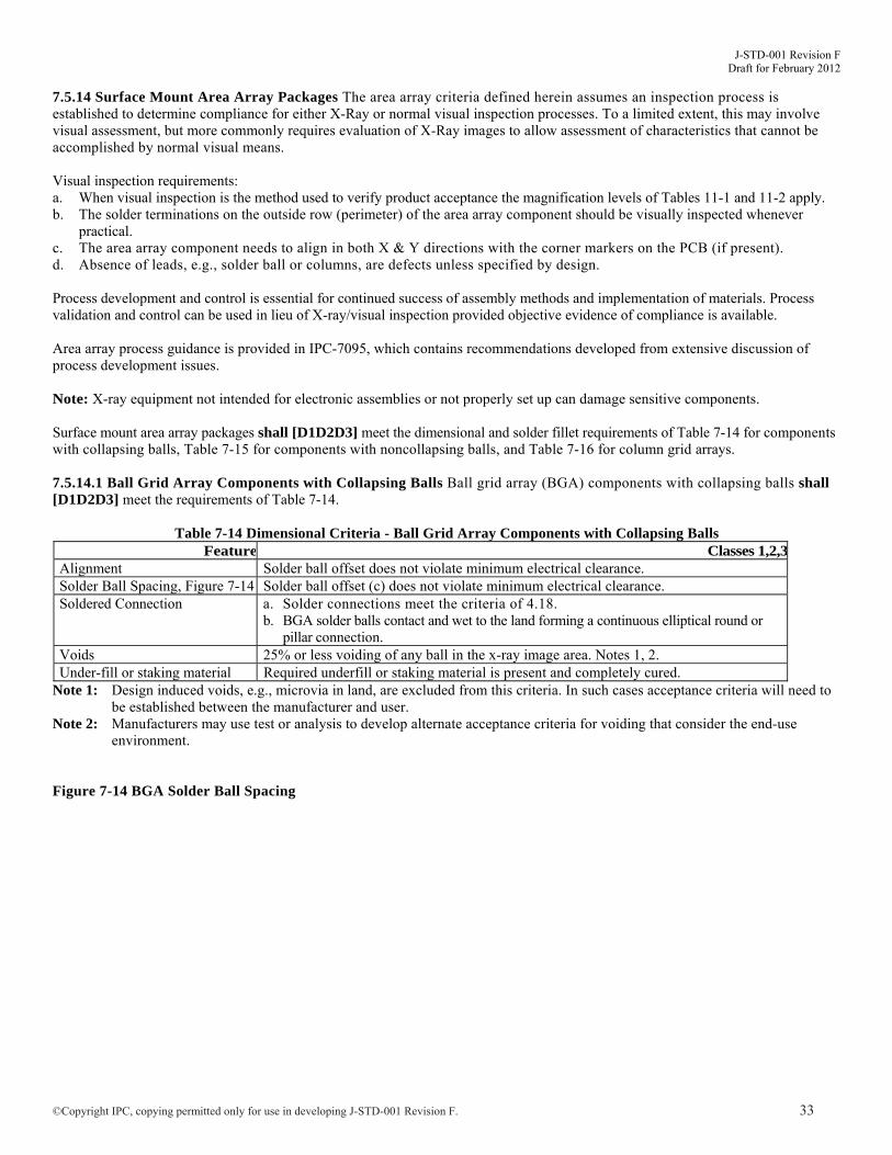
J-STD-001 Revision F Draft for February 2012
©Copyright IPC, copying permitted only for use in developing J-STD-001 Revision F. 33
7.5.14 Surface Mount Area Array Packages The area array criteria defined herein assumes an inspection process is established to determine compliance for either X-Ray or normal visual inspection processes. To a limited extent, this may involve visual assessment, but more commonly requires evaluation of X-Ray images to allow assessment of characteristics that cannot be accomplished by normal visual means. Visual inspection requirements: a. When visual inspection is the method used to verify product acceptance the magnification levels of Tables 11-1 and 11-2 apply. b. The solder terminations on the outside row (perimeter) of the area array component should be visually inspected whenever
practical. c. The area array component needs to align in both X & Y directions with the corner markers on the PCB (if present). d. Absence of leads, e.g., solder ball or columns, are defects unless specified by design. Process development and control is essential for continued success of assembly methods and implementation of materials. Process validation and control can be used in lieu of X-ray/visual inspection provided objective evidence of compliance is available. Area array process guidance is provided in IPC-7095, which contains recommendations developed from extensive discussion of process development issues. Note: X-ray equipment not intended for electronic assemblies or not properly set up can damage sensitive components. Surface mount area array packages shall [D1D2D3] meet the dimensional and solder fillet requirements of Table 7-14 for components with collapsing balls, Table 7-15 for components with noncollapsing balls, and Table 7-16 for column grid arrays. 7.5.14.1 Ball Grid Array Components with Collapsing Balls Ball grid array (BGA) components with collapsing balls shall [D1D2D3] meet the requirements of Table 7-14.
Table 7-14 Dimensional Criteria - Ball Grid Array Components with Collapsing Balls Feature Classes 1,2,3
Alignment Solder ball offset does not violate minimum electrical clearance. Solder Ball Spacing, Figure 7-14 Solder ball offset (c) does not violate minimum electrical clearance. Soldered Connection a. Solder connections meet the criteria of 4.18.
b. BGA solder balls contact and wet to the land forming a continuous elliptical round or pillar connection.
Voids 25% or less voiding of any ball in the x-ray image area. Notes 1, 2. Under-fill or staking material Required underfill or staking material is present and completely cured.
Note 1: Design induced voids, e.g., microvia in land, are excluded from this criteria. In such cases acceptance criteria will need to be established between the manufacturer and user.
Note 2: Manufacturers may use test or analysis to develop alternate acceptance criteria for voiding that consider the end-use environment.
Figure 7-14 BGA Solder Ball Spacing

J-STD-001 Revision F Draft for February 2012
©Copyright IPC, copying permitted only for use in developing J-STD-001 Revision F. 34
7.5.14.2 Ball Grid Array Components with Noncollapsing Balls Ball grid array components with noncollapsing balls shall [D1D2D3] meet the requirements of Table 7-15.
Table 7-15 Ball Grid Array Components with Noncollapsing Balls Feature Classes 1,2,3
Alignment Solder ball offset does not violate minimum electrical clearance.
Soldered Connection a. Solder connections meet the criteria of 4.18 b. Solder is wetted to the solder balls and land terminations.
Under-fill or staking material Required underfill or staking material is present and completely cured. 7.5.14.3 Column Grid Array Components Column grid array (CGA) components shall [D1D2D3] meet the requirements of Table 7-16.
Table 7 16 Column Grid Array Feature Class 1 Classes 2,3
Alignment Column offset does not violate minimum electrical clearance.
Column perimeter does not extend beyond the perimeter of the land.
Solder connections Meet the criteria of 4.18 External columns show complete filleting for the portions of the columns that are visible
Under-fill or staking material Required underfill or staking material is present and completely cured. 7.5.15 Bottom Termination Components (BTC) These criteria are also applicable to Small Outline Integrated Circuit (No Leads) [SOICNL]. Criteria for nonvisible part of thermal plane solder connections are not described in this document and will need to be established by agreement between the user and the manufacturer. The thermal transfer plane acceptance criteria are design and process related. Issues to consider include but are not limited to component manufacturer’s application notes, solder coverage, voids, solder height, etc. When soldering these types of components voiding in the thermal plane is common. Solder, when required, shall [D1D2D3] meet documented requirements. Connections formed to components having no significant external lead form shall [D1D2D3] meet the dimensional and solder fillet requirements of Table 7-17 and Figure 7-15. There are some package configurations that have no toe exposed or do not have a continuous solderable surface on the exposed toe on the exterior of the package and a toe fillet will not form. Bottom Termination Component (BTC) process guidance is provided in IPC-7093, which contains recommendations developed from extensive discussion of BTC process development issues. Process development and control is essential for continued success of assembly methods and implementation of materials. Process validation and control can be used in lieu of X-ray/visual inspection provided objective evidence of compliance is available.

J-STD-001 Revision F Draft for February 2012
©Copyright IPC, copying permitted only for use in developing J-STD-001 Revision F. 35
Table 7-17 Dimensional Criteria - BTC
Feature Dim. Class 1 Class 2 Class 3 Maximum Side Overhang A 50% (W), Note 1 25% (W), Note 1
Toe Overhang (outside edge of component termination)
B Not Permitted`
Minimum End Joint Width C 50% (W) 75% (W) Minimum Side Joint Length D Note 4 Solder Fillet Thickness G Note 3 Minimum Toe (End) Fillet Height F Notes 2, 5 Notes 2, 5 Termination Height H Note 5
Solder coverage of thermal land Note 4 Land Width P Note 2
Termination Width W Note 2 Thermal Plane Void Criteria Note 6
Note 1: Does not violate minimum electrical clearance. Note 2: Unspecified parameter or variable in size as determined by design. Note 3: Wetting is evident. Note 4: Not a visually inspectable attribute. See 4.18.3. Note 5: “H”= height of solderable surface of lead, if present. Some package configurations do not have a continuous solderable surface on the
sides and do not require a toe (end) fillet. Note 6: Acceptance criteria will need to be established between the manufacturer and user. Figure 7-15 Bottom Termination Component 7.5.16 Components with Bottom Thermal Plane Terminations (D-Pak) Criteria for nonvisible part of thermal plane solder connections are not described in this document and will need to be established by agreement between the user and the manufacturer. The thermal transfer plane acceptance criteria are design and process related. Issues to consider include but are not limited to component manufacturer’s application notes, solder coverage, voids, solder height, etc. Solder, when required, shall [D1D2D3] meet documented requirements. When soldering these types of components voiding in the thermal plane is common. Note: The criteria for leads other than the thermal plane termination are provided in the criteria for the type of lead termination used. Connections formed to components with bottom thermal plane terminations shall [D1D2D3] meet the dimensional and solder fillet requirements of Table 7-18.
Table 7-18 Dimensional Criteria - Bottom Thermal Plane Terminations Feature (all connections except thermal plane) Dim.
The mounting and solder requirements for SMT terminations shall [D1D2D3] meet the criteria for the
type of lead termination being used.
Maximum Side Overhang A Toe Overhang B Minimum End Joint Width C Minimum Side Joint Length D Maximum Heel Fillet Height E Minimum Heel Fillet Height F Solder Fillet Thickness G Lead Thickness T
Feature (only for the thermal plane connection) Class 1,2,3 Thermal Plane Side Overhang (Figure 7-16) Not greater than 25% of termination width. Thermal Plane End Overhang No overhang. Thermal Plane End Joint Width 100% wetting to land in the end-joint contact area.
Figure 7-16 Bottom Thermal Plane Termination

J-STD-001 Revision F Draft for February 2012
©Copyright IPC, copying permitted only for use in developing J-STD-001 Revision F. 36
7.5.17 Flattened Post Connections This termination style is sometimes referred to as nail-head pin. Criteria have not been established for Class 3 for this termination style. Process development and control is essential for continued success of assembly methods and implementation of materials. Connections formed to components with flattened post connections (Figure 7-17) shall [D1D2N3] meet the dimensional and solder fillet requirements of Table 7-19.
Table 7-19 Dimensional Criteria Flattened Post Connections Feature Class 1 Class 2 Class 3 Maximum Termination Overhang, Square Solder Land
75% Termination Width (W), Notes 1, 2
50% Termination Width (W), Notes 1, 2
Criteria not established
Maximum Termination Overhang, Round Solder Land
50% Termination Width (W), Notes 1, 2
25% Termination Width (W), Notes 1, 2
Maximum Fillet Height Note 4 Minimum Fillet Height Note 3 Note 1: Does not violate minimum electrical clearance. Note 2: Lead diameter is less than diameter or side length of the solder land. Note 3: Wetting is evident. Note 4: Solder does not touch component body. Figure 7-17 Flattened Post Termination 7.5.18 P-Style Connections P-Style termination has a soldering termination that resembles the letter “P”. This is typically found on edge mounted connectors that will be soldered on both sides of the board. Precursor Requirements: Criteria established for Class 3 assemblies At no time may there be any violation of Minimum Electrical Clearance (MEC) Lead damage criteria is per current IPC/J-STD requirements Maximum Side Overhang (A) ACCEPTABLE: 25% (W) or 0.5 mm (0.02 in), whichever is less DEFECT: Greater than 25% (W) or 0.5 mm (0.02 in), whichever is less
Maximum Toe Overhang (B) ACCEPTABLE: Per design, with no violation of MEC DEFECT: Any violation of MEC Minimum End Joint Width (C) ACCEPTABLE: 75% (W) Wetted with Solder DEFECT: Less than 75% (W) wetted with Solder Minimum Side Joint Length (D) ACCEPTABLE: 100% (L) wetted with solder (“P” is wetted with solder) DEFECT: Less than 100% (L) wetted with solder

J-STD-001 Revision F Draft for February 2012
©Copyright IPC, copying permitted only for use in developing J-STD-001 Revision F. 37
Maximum Fillet Height (E) No violation of MEC Minimum Fillet Height (F) ACCEPTABLE: G + Thickness of Contact Area (ABOVE YELLOW LINE ON IMAGE) “P” portion is embedded in wetted solder
Solder Thickness (G) Unspecified and Un-measurable dimension Contact Area / Foot Length (L) P-shaped area of lead. Dimension varies with design (Red outlined area represents the “contact area” or Length that must be embedded in wetted solder)
Lead Thickness (T) Unspecified dimension, or variable in size as determined by design Lead Width (W) Unspecified dimension, or variable in size as determined by design

J-STD-001 Revision F Draft for February 2012
©Copyright IPC, copying permitted only for use in developing J-STD-001 Revision F. 38
7.6 Specialized SMT Terminations The IPC committee that maintains this standard has received requests to include a number of specialized SMT termination styles. Often these termination styles are unique to a particular component or are specially made for a limited number of users. Before acceptance criteria can be developed there needs to be significant use so that a history of failure data can be captured from multiple users. Clause 1.13.2 of this standard is repeated here.
1.13.2 Procedures for Specialized Technologies As an industry consensus standard, this document cannot address all of the possible components and product design combinations, e.g., magnetic windings, high frequency, high voltage, etc. Where uncommon or specialized technologies are used, it may be necessary to develop unique process and/or acceptance criteria. Often, unique definition is necessary to consider the specialized characteristics while considering product performance criteria. The development should include user involvement. The acceptance criteria shall [N1N2D3] have user agreement. Mounting and soldering requirements for specialized processes and/or technologies not specified herein shall [N1D2D3] be performed in accordance with documented procedures which are available for review. Whenever possible these criteria should be submitted to the IPC Technical Committee to be considered for inclusion in upcoming revisions of this standard.
8 CLEANING PROCESS REQUIREMENTS An item that is required to be cleaned shall [N1N2D3] be cleaned per a documented process to allow removal of all contaminants (especially flux residue). The items cleaned shall [D1D2D3] be capable of meeting the cleanliness requirement as specified herein (see 8.3). All items to be cleaned shall [D1D2D3] be cleaned in a manner that will prevent thermal shock and/or detrimental intrusion of cleaning media into components that are not totally sealed. 8.1 Cleanliness Exemptions Terminations internal to self-sealing devices (e.g., heat shrinkable solder devices) are exempt from the cleaning requirements of this standard when the device encapsulates the solder connection. 8.2 Ultrasonic Cleaning Ultrasonic cleaning is permissible: a. On bare boards or assemblies, provided only terminals or connectors without internal electronics are present. b. On electronic assemblies with electrical components, provided the manufacturer has documentation available for review showing
that the use of ultrasonics does not damage the mechanical or electrical performance of the product or components being cleaned, see IPC-TM-650, Test Method 2.6.9.1, Test to Determine Sensitivity of Electronic Assemblies to Ultrasonic Energy and Test Method 2.6.9.2, Test to Determine Sensitivity of Electronic Components to Ultrasonic Energy.
8.3 Post-Solder Cleanliness Inspection is used to assess the presence of visible foreign particulate matter as required in 8.3.1, or flux and other ionic or organic residues as required in 8.3.2 (see 11.2.2). 8.3.1 Particulate Matter Assemblies shall [D1D2D3] be free of dirt, lint, solder webbing, dross, wire clippings, etc. Solder balls or solder splash shall [D1D2D3] neither be loose (i.e., be dislodged in the normal service environment of the product) nor violate minimum electrical clearance. 8.3.2 Flux Residues and Other Ionic or Organic Contaminants Unless specified by the user, the manufacturer should specify a cleanliness designator that establishes the cleaning option and test for cleanliness in accordance with 8.3.3 and in compliance with 3, Materials, Components and Equipment Requirements. In the absence of a specified cleanliness designator, the designator C-22 as described in the following paragraphs and the visual requirements for cleanliness shall [D1D2D3] apply. Note: This requirement may be eliminated when visible residue has been identified as benign through laboratory analysis or other means. 8.3.3 Post-Soldering Cleanliness Designator The cleanliness designator is to be in the following form: A 2-digit (minimum) code describes the cleanliness requirements for all assemblies covered under this standard. This code begins with the letter “C” then a dash followed by two or more digits. The first digit represents the cleaning option described in 8.3.4 and the second and following digits indicate the requirements for cleanliness testing described in 8.3.5.

J-STD-001 Revision F Draft for February 2012
©Copyright IPC, copying permitted only for use in developing J-STD-001 Revision F. 39
8.3.4 Cleaning Option The first digit of the cleanliness designator defines the cleaning option. The digits in Table 8-1 are used to define the surfaces of the assembly that are to be cleaned.
Table 8-1 Designation of Surfaces to be Cleaned 0 No surfaces to be cleaned 1 One side (solder source side) of assembly to be cleaned 2 Both sides of assembly to be cleaned
8.3.5 Test for Cleanliness The second and following digits of the cleanliness designator define the requirements for cleanliness testing. The digits in Table 8-2 apply.
Table 8-2 Cleanliness Testing Designators 0 No test for cleanliness required 1 Test for rosin residues required (8.3.6.1) 2 Test for ionic residues required (8.3.6.2 and/or 8.3.6.3) 3 Test for surface insulation resistance (8.3.6.4) 4 Test for other surface organic contaminants (8.3.6.5) 5 Other tests as defined by user/manufacturer agreement
8.3.6 Testing If required, periodic testing of cleanliness of the printed circuit assemblies after final cleaning (e.g., the cleaning prior to conformal coating, encapsulation, or incorporation into the next higher assembly) shall [D1D2D3] be conducted on a random sample basis (see 11.2.3) to ensure the adequacy of the cleaning process(es). If any printed circuit assembly fails, the entire lot shall [D1D2D3] be evaluated and recleaned if necessary and a random sample of this lot and each lot cleaned since performing the last acceptable cleanliness test shall [D1D2D3] be tested. The frequency of testing shall [N1P2D3] be a minimum of once each production shift unless the process control system data supports a change in frequency. 8.3.6.1 Rosin Flux Residues When rosin flux residue testing is required, assemblies shall [D1D2D3] be tested in accordance with IPC-TM-650, Test Method 2.3.27 and shall [D1D2D3] comply with the following requirements for the maximum allowable level of flux residues: Class 1 assemblies less than 200 micrograms/cm2
Class 2 assemblies less than 100 micrograms/cm2
Class 3 assemblies less than 40 micrograms/cm2 8.3.6.2 Ionic Residues (Instrument Method) When ionic residue (instrument method) testing is required, assemblies shall [D1D2D3] be tested in accordance with IPC-TM-650, Method 2.3.25, Detection and Measurement of Ionizable Surface Contaminants. Dynamic Extraction Methods should be performed in compliance with Test Method 2.3.25, item 5. Static Extraction Methods should be performed in compliance with Test Method 2.3.25, item 6. Other methods may be used when the sensitivity of the alternative method is shown to be equal to or better than the above methods with respect to detecting ionizable surface contamination. In comparing the sensitivity between methods, the solvent used to extract the residue, the method used to present the solvent to the assembly, and the method of detecting the residue should all be considered. For assemblies soldered with ROL0 or ROL1 fluxes, and tested by Static Extraction Method, contamination shall [D1D2D3] be less than 1.56 micrograms/cm2 sodium chloride (NaCl) equivalent ionic or ionizable flux residue. When another test method or flux is used (see 3.3), contamination shall not [D1D2D3] exceed a limit to be established by the manufacturer or by the user. When established by the manufacturer, the limit shall [D1D2D3] be supported by historical data (indicating that the cleaning and testing processes are proven, well established, and in control), or by process qualification test data (see 3.1) that are available for review. 8.3.6.3 Ionic Residues (Manual Method) When ionic residue (manual method) testing is required, assemblies shall [D1D2D3] be tested in accordance with IPC-TM-650, Test Method 2.3.25, Detection and Measurement of Ionizable Surface Contaminants. For assemblies soldered with ROL0 or ROL1 fluxes, surface contamination shall [D1D2D3] be less than 1.56 micrograms/cm2 NaCl equivalent ionic or ionizable flux residue. When another flux is used (see 3.3), contamination shall not [D1D2D3] exceed a limit to be established by the manufacturer or by the user. When established by the manufacturer, the limit shall [D1D2D3] be supported by

J-STD-001 Revision F Draft for February 2012
©Copyright IPC, copying permitted only for use in developing J-STD-001 Revision F. 40
historical data (indicating that the cleaning process is proven, well established, and in control), or by process qualification test data (see 3.1) that are available for review. 8.3.6.4 Surface Insulation Resistance (SIR) When surface insulation resistance testing (SIR) is required, it shall [D1D2D3] be performed using a documented method that includes pass/fail criteria and is available for review. See IPC-9201. 8.3.6.5 Other Contamination When surface organic contamination testing is required, assemblies tested in accordance with IPC-TM-650, Test Method 2.3.39, Surface Organic Contamination Identification Test (Infrared Analytical Method) shall not [D1D2D3] exceed the maximum acceptance level established by mutual agreement between user and manufacturer. 9 PCB REQUIREMENTS This section applies to PCB defects regardless of when they occur in the assembly process. 9.1 Printed Circuit Board Damage 9.1.1 Blistering/Delamination Blistering or delamination(s) shall not [D1D2D3] exceed 25% of the distance between plated-through holes or internal conductors or reduce the space between conductive patterns to less than the minimum electrical clearance. Note: Blisters or delamination areas may propagate during assembly or operation. Separate criteria may need to be established. Measling is NOT the same as blistering and/or delamination. See IPC-T-50 and IPC-A-610 for clarification. 9.1.2 Weave Exposure/Cut Fibers Weave exposure shall not [D1D2D3] reduce the clearance between noncommon conductive patterns to less than the minimum electrical clearance. There shall [N1D2D3] be no surface damage that cuts into laminate fibers. 9.1.3 Haloing Penetration of haloing or edge delamination shall not [D1D2D3] affect the physical spacing from the edge to the closest conductive pattern by more than 50% or more than 2.5 mm [0.0984 in], whichever is less. 6012C 3.3.1: The distance between the haloing penetration and the nearest conductive feature shall not be less than the minimum lateral conductor spacing, or 100 μm [3,937 μin] if not specified. 9.1.4 Land Separation The outer, lower edge of land areas shall not [D1D2D3] be lifted or separated more than the thickness (height) of the land. For Class 3 assemblies, the land areas shall not [N1N2D3] be lifted when there is an unfilled via or via with no lead in the land. 9.1.5 Land/Conductor Reduction in Size The width of printed conductors or width/ length of lands shall not [D1D2D3] be reduced by more than 20% for Class 2 and 3 and 30% for Class 1(see IPC-A-600, IPC-6011 and IPC-6012). 9.1.6 Flexible Circuitry Delamination Separation or bubbles shall not [D1D2D3] bridge conductors in the cover layer of flexible printed circuit boards or assemblies. 9.1.7 Flexible Circuitry Damage There shall not [D1D2D3] be evidence of tearing, blistering, charring, or melting of the insulation. Nicks shall not [D1D2D3] extend deeper than 50% of the distance from the edge to the nearest conductor or 2.5 mm [0.0984 in], whichever is less. Note: Mechanically created indentions caused by contact between the coverlayer of flexible printed circuit boards or assemblies and molten solder are not rejectable. Additionally, care should be taken to avoid bending or flexing conductors during inspection. 9.1.8 Burns Burns shall not [D1D2D3] physically damage the surface of the assembly. 9.1.9 Solder on Gold Contacts Solder shall not [D1D2D3] be in the contact area of gold edge connector contact lands (i.e., “gold fingers”). 9.1.10 Measles Measling is acceptable for Class 1, 2 and 3 printed board assemblies. Measled areas in laminate substrates shall not [N1N2P3] exceed 50% of the spacing between noncommon conductors. Note: Measling is an internal condition which may not propagate under thermal stress and has not been conclusively shown to be a catalyst for conductive anodic filament (CAF) growth. Delamination is an internal condition which may propagate under thermal stress and may be a catalyst for CAF growth. The IPC-9691 user’s guide for CAF resistance testing and IPCTM-650, Method 2.6.25, provide additional information for determining laminate performance regarding CAF growth. Users who wish to incorporate additional

J-STD-001 Revision F Draft for February 2012
©Copyright IPC, copying permitted only for use in developing J-STD-001 Revision F. 41
criteria for measle conditions may consider incorporating the provisions of IPC-6012, Appendix A which does not allow measles for Class 3 product. Note: Visual aids can be found in IPC-A-610 and IPC-HDBK-001. 9.2 Marking Assembly identification such as part numbers and serial numbers shall [N1D2D3] remain legible (capable of being read and understood) after all tests, cleaning and other processes to which the item is subjected. Additional markings (such as labels added during the manufacturing process) should not obscure the original supplier’s markings. Individual component markings, reference designators and polarity indicators should remain legible and components should be mounted in such a manner that markings are visible. 9.3 Bow and Twist (Warpage) Bow and twist after soldering should not exceed 1.5% for through-hole, or 0.75% for surface mount printed board applications (see IPC-TM 650, 2.4.22). Bow and twist shall not [D1D2D3] cause damage during post solder assembly operations or use. 10 COATING, ENCAPSULATION AND STAKING (ADHESIVE) When coating or encapsulation materials are applied to glass body components, the components shall [D1D2D3] be sleeved to prevent cracking, unless the material has been selected so as not to damage the components/assembly in its service environment. The material specification or other documented procedure shall [D1D2D3] be followed for mixing and curing. The material shall [D1D2D3] be used within the time period specified (both shelf life and pot life) or used within the time period indicated by a documented system the manufacturer has established to mark and control age-dated material. Equipment used for measuring viscosity, mixing, applying and or curing silicone material shall not [D1D2D3] be used for processing other material. >Sep2011> 10.1 Conformal Coating Conformal coating material shall [D1D2D3] conform to the material specification (IPC-CC-830 or equivalent). The coating manufacturers supplier’s instructions or other documented process shall [D1D2D3] be followed. When curing conditions (temperature, time, Infra Red (I.R.) intensity, etc.) vary from supplier recommended instructions, they shall [D1D2D3] be documented and available for review. The material shall [D1D2D3] be used within the time period specified (both shelf life and pot life) or used within the time period indicated by a documented system the manufacturer (assembler) has established to mark and control age-dated material. 10.1.1 Application Coating shall [D1D2D3] be applied in a continuous manner to all areas designated for coverage on the assembly drawing/documentation. The coating fillets should be kept to a minimum. When used, masking materials shall [D1D2D3] have no deleterious effect and shall [D1D2D3] be removable without leaving contaminant residue. Dimensions of masked areas shall not [D1D2D3] be decreased in length, width, or diameter by more than 0.75 mm [0.0295 in] by application of conformal coating. 10.1.1.1 Components Required to be Uncoated The adjustable portion of adjustable components, as well as electrical and mechanical mating surfaces such as connector contacts, probe points, screw threads, bearing surfaces (e.g., card guides) shall [D1D2D3] be left uncoated as specified on the assembly drawing(s)/ documentation. 10.1.1.2 Conformal Coating on Connectors Mating connector surfaces of printed circuit assemblies shall [D1D2D3] be free of conformal coating. 10.1.1.3 Conformal Coating on Brackets The mating (contact) surface of brackets or other mounting devices shall not [D1D2D3] be coated with conformal coating unless specifically required by the assembly drawing(s)/documentation. 10.1.1.4 Conformal Coating for Tin Whisker Risk Mitigation Conformal coating used for the purpose of tin whisker risk mitigation will be documented in terms of conformal coating thickness and coverage. The documented objective evidence shall [N1D2D3] be available for review. 10.1.2 Performance Requirements

J-STD-001 Revision F Draft for February 2012
©Copyright IPC, copying permitted only for use in developing J-STD-001 Revision F. 42
10.1.2.1 Thickness The thickness of the conformal coating shall [D1D2D3] be as shown in Table 10-1 for the type specified (see IPC-2221): Note: Table 10-1 of this standard is to be used for printed circuit assemblies. The coating thickness requirements in IPC-CC-830 Table 4-2 are to be used only for test vehicles associated with coating material testing and qualification.
Table 10-1 Coating Thickness Type AR Acrylic Resin 0.03-0.13 mm [0.00118 to 0.00512 in] Type ER Epoxy Resin 0.03-0.13 mm [0.00118 to 0.00512 in] Type UR Urethane Resin 0.03-0.13 mm [0.00118 to 0.00512 in] Type SR Silicone Resin 0.05-0.21 mm [0.00197 to 0.00827 in] Type XY Paraxylylene Resin 0.01-0.05 mm [0.000394 to 0.00197 in]
The thickness is measured on a flat, unencumbered, cured surface of the printed circuit assembly or a coupon that has been processed with the assembly. Coupons may be of the same type of material as the printed board or may be of a nonporous material such as metal or glass. As an alternative, wet film or viscosity measurement may be used to establish the coating thickness provided there is documentation that correlates dry film thickness to the alternate measurement technique. 10.1.2.2 Coating Coverage Conformal coating shall [D1D2D3]: a. Be completely cured and homogeneous. b. Cover only those areas specified on the assembly drawing(s)/documentation. c. Be free of blisters, or breaks that could affect the operations of the assembly or sealing properties of the conformal coating. d. Be free of cracks, crazing, voids, bubbles, mealing, peeling, wrinkles or foreign material which expose component conductors,
printed circuit conductors, (including ground planes) or other conductors and/or violates design electrical clearance.
10.1.3 Conformal Coating Inspection Inspection of conformal coating shall [A1P2D3] be performed (see Table 11-2) and may be performed without magnification. Inspection for conformal coating coverage may be performed under an ultraviolet (UV) light source when using conformal coating material containing a UV tracer. Magnification up to 4X may be used for referee purposes. 10.1.4 Rework of Conformal Coating Procedures which describe the removal and replacement of conformal coating shall [N1D2D3] be documented and available for review. 10.2 Encapsulation The material specification and supplier’s instructions, as applicable, shall [D1D2D3] be followed. The material shall [D1D2D3] be used within the time period specified (both shelf life and pot life) or used within the time period indicated by a documented system the manufacturer has established to mark and control age-dated material. 10.2.1 Application Encapsulant material shall [D1D2D3] be applied in a continuous manner to all areas designated for coverage on the assembly drawing/ documentation. When used, masking material shall [D1D2D3] have no deleterious effect on the printed boards and shall [D1D2D3] be removable without contaminant residue. 10.2.1.1 Encapsulant Free Surfaces All portions of the assembly not designated to receive encapsulant material shall [D1D2D3] be free of any encapsulant material. 10.2.2 Performance Requirements The applied encapsulant shall [N1D2D3] be completely cured, homogeneous, and cover only those areas specified on the assembly drawing(s)/documentation. The encapsulant shall [D1D2D3] be free of bubbles, blisters, or breaks that affect the assembly operation or sealing properties of the encapsulant material. There shall [N1P2D3] be no visible cracks, crazing, mealing, peeling, and/or wrinkles in the encapsulant material. Minor surface swirls, striations, or flow marks are not considered defects. 10.2.3 Rework of Encapsulant Material Procedures which describe the removal and replacement of encapsulant material shall [N1N2D3] be documented and available for review. 10.2.4 Encapsulant Inspection Visual inspection of encapsulation shall [A1P2D3] be performed per 11.2. 10.3 Staking (Adhesive) The criteria below shall [D1D2D3] be used when staking is required and criteria are not provided on the drawing.

J-STD-001 Revision F Draft for February 2012
©Copyright IPC, copying permitted only for use in developing J-STD-001 Revision F. 43
a. Placement – Staking materials shall not [P1D2D3] contact component lead seals unless the material has been selected so as not to damage the components/assembly in its service environment.
b. Unsleeved axial leaded components mounted horizontally – Staking material shall [N1N2D3] be applied to both sides of the component. The length of the fillets of the staking material shall [D1D2D3] extend between 50% and 100% of the component length. Minimum fillet height shall [D1D2D3] be 25% of the height of the component. For maximum fillet height, the top of the component shall [N1P2D3] be visible for the entire length of the component body.
c. Unsleeved axial leaded components mounted vertically – A minimum of two beads of staking material shall [N1D2D3] be placed approximately evenly around the periphery of the component. For each bead, the staking material shall [N1D2D3] contact a minimum-25% to maximum-100% of the height of the component body. Slight flow of staking material under the component body is acceptable provided it does not violate 10.3a. Adhesive shall [D1D2D3] adhere to at least 25% of the component circumference.
d. Sleeved axial leaded components – Staking material shall [P1D2D3] be in contact with both end-faces of the component and the surface it is being staked to. Minimum fillet height shall [P1D2D3] be at least 25% of the component height. Maximum fillet height shall [P1D2D3] be no greater than 50% of the component height, and shall [P1D2D3] meet the requirements of 10.3a. This clause does not apply to sleeved glass bodied axial leaded components (see 10.3e).
e. Glass bodied components – Sleeved glass bodied components shall [P1D2D3] be free from staking material on any exposed glass surface, such as the component end face. Staking material shall [N1N2D3] be applied to both sides of the component. Staking material fillet shall [P1D2D3] extend between 50% and 100% of the component length. Minimum fillet height shall [D1D2D3] be 25% of the component height. Maximum fillet height shall [N1P2D3] allow the top of the component to be visible for the entire length of the component body.
f. Radial leaded components whose longest dimension is their height (e.g., CKR capacitors, Single In-Line (SIP) resistor networks) – The staking material shall [N1D2D3] be applied to a minimum height of 25% to a maximum of 100% of each individual component’s body height. <Sep2011>
For closely spaced arrays consisting of up to four components fillet height requirements for the two outer end-faces shall [N1D2D3] be the same as for an individual component. In addition, the top inner surfaces shall [N1D2D3] be bonded to each other for 50% of the components’ width.
For closely spaced arrays consisting of more than four components staking shall [N1D2D3] be applied in the same manner as arrays up to four components, with the additional requirement that every other internal component shall [N1D2D3] have their sides staked to the board surface.
g. Radial leaded components whose longest dimension is their diameter or length (e.g., TO5 semiconductors, etc.) – Cylindrical components shall [N1D2D3] be staked with at least three beads of staking material placed approximately evenly around the periphery of the component. For each bead, the staking material shall [N1D2D3] contact a minimum-25% to maximum-100% of the height of the component body. Slight flow of staking material under the component body is acceptable provided it does not violate 10.3a.
Rectangular components shall [N1D2D3] be staked with a bead of staking material placed at each corner of the component. For each bead, the staking material shall [N1D2D3] contact a minimum-25% to maximum-100% of the height of the component body. Slight flow of staking material under the component body is acceptable provided it does not violate 10.3a.
h. Fasteners identified on the drawing to be staked shall [D1D2D3] be staked either: a. At two places spaced approximately opposite of each other, with beads of staking material covering at least 25% of the
perimeter of the fastener. b. With one bead of staking material covering at least 50% of the perimeter of the fastener.
10.3.1 Staking Staking shall [D1D2D3]: a. Be completely cured and homogeneous. b. Be free of voids or bubbles that expose component conductors, bridge noncommon conductors and/or violate design electrical
clearance. c. Not bridge between the substrate and the bottom of radial leaded components. This does not apply to bonding or under-filling
when used as part of a documented process. d. Be free of contamination. e. Not negate stress relief.
10.3.2 Staking (Inspection) Visual inspection of staking may be performed without magnification. Magnification from 1.75X to 4X may be used for referee purposes. 11 PRODUCT ASSURANCE
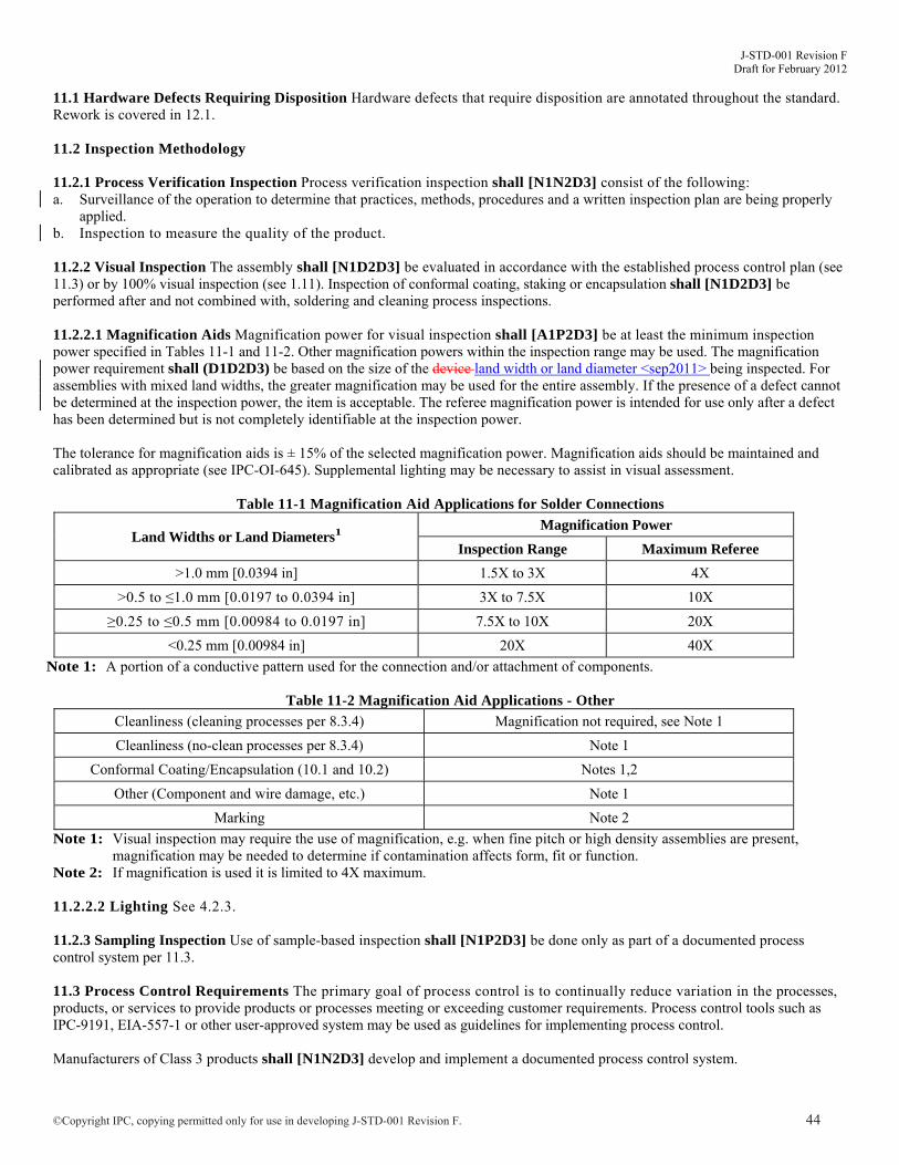
J-STD-001 Revision F Draft for February 2012
©Copyright IPC, copying permitted only for use in developing J-STD-001 Revision F. 44
11.1 Hardware Defects Requiring Disposition Hardware defects that require disposition are annotated throughout the standard. Rework is covered in 12.1. 11.2 Inspection Methodology 11.2.1 Process Verification Inspection Process verification inspection shall [N1N2D3] consist of the following: a. Surveillance of the operation to determine that practices, methods, procedures and a written inspection plan are being properly
applied. b. Inspection to measure the quality of the product.
11.2.2 Visual Inspection The assembly shall [N1D2D3] be evaluated in accordance with the established process control plan (see 11.3) or by 100% visual inspection (see 1.11). Inspection of conformal coating, staking or encapsulation shall [N1D2D3] be performed after and not combined with, soldering and cleaning process inspections. 11.2.2.1 Magnification Aids Magnification power for visual inspection shall [A1P2D3] be at least the minimum inspection power specified in Tables 11-1 and 11-2. Other magnification powers within the inspection range may be used. The magnification power requirement shall (D1D2D3) be based on the size of the device land width or land diameter <sep2011> being inspected. For assemblies with mixed land widths, the greater magnification may be used for the entire assembly. If the presence of a defect cannot be determined at the inspection power, the item is acceptable. The referee magnification power is intended for use only after a defect has been determined but is not completely identifiable at the inspection power. The tolerance for magnification aids is ± 15% of the selected magnification power. Magnification aids should be maintained and calibrated as appropriate (see IPC-OI-645). Supplemental lighting may be necessary to assist in visual assessment.
Table 11-1 Magnification Aid Applications for Solder Connections
Land Widths or Land Diameters1 Magnification Power
Inspection Range Maximum Referee
>1.0 mm [0.0394 in] 1.5X to 3X 4X
>0.5 to ≤1.0 mm [0.0197 to 0.0394 in] 3X to 7.5X 10X
≥0.25 to ≤0.5 mm [0.00984 to 0.0197 in] 7.5X to 10X 20X
<0.25 mm [0.00984 in] 20X 40X
Note 1: A portion of a conductive pattern used for the connection and/or attachment of components.
Table 11-2 Magnification Aid Applications - Other
Cleanliness (cleaning processes per 8.3.4) Magnification not required, see Note 1
Cleanliness (no-clean processes per 8.3.4) Note 1
Conformal Coating/Encapsulation (10.1 and 10.2) Notes 1,2
Other (Component and wire damage, etc.) Note 1
Marking Note 2
Note 1: Visual inspection may require the use of magnification, e.g. when fine pitch or high density assemblies are present, magnification may be needed to determine if contamination affects form, fit or function.
Note 2: If magnification is used it is limited to 4X maximum. 11.2.2.2 Lighting See 4.2.3. 11.2.3 Sampling Inspection Use of sample-based inspection shall [N1P2D3] be done only as part of a documented process control system per 11.3. 11.3 Process Control Requirements The primary goal of process control is to continually reduce variation in the processes, products, or services to provide products or processes meeting or exceeding customer requirements. Process control tools such as IPC-9191, EIA-557-1 or other user-approved system may be used as guidelines for implementing process control. Manufacturers of Class 3 products shall [N1N2D3] develop and implement a documented process control system.

J-STD-001 Revision F Draft for February 2012
©Copyright IPC, copying permitted only for use in developing J-STD-001 Revision F. 45
A documented process control system, if established, shall [N1D2D3] define process control and corrective action limits. This may or may not be a “statistical process control” system. The use of “statistical process control”(SPC) is optional and should be based on factors such as design stability, lot size, production quantities, and the needs of the manufacturer (see 11.4). Process control methodologies shall [N1D2D3] be used in the planning, implementation and evaluation of the manufacturing processes used to produce soldered electrical and electronic assemblies. The philosophy, implementation strategies, tools and techniques may be applied in different sequences depending on the specific company, operation, or variable under consideration to relate process control and capability to end product requirements. When a decision or requirement is to use a documented process control system, failure to implement process corrective action and/or the use of continually ineffective corrective actions shall [N1D2D3] be grounds for disapproval of the process and associated documentation. 11.3.1 Opportunities Determination Unless otherwise specified in the process control plan, the total number of interconnection sites is used as the measure to which the percentage of defects or process indicators is applied. These calculations consider each surface mount termination, each through-hole termination, and each terminal termination as a single opportunity in determining the total number of opportunities for a given printed board assembly. For corrective action calculations, no more than one defect characteristic or process indicator can be attributed to a particular interconnection site (e.g., via, lead-in-hole, lead-to-land). For more information (see IPC-9261). 11.4 Statistical Process Control The use of “statistical process control”is encouraged but not mandatory (see 11.3). When a statistical process control system process is used, it shall [D1D2D3] include the following elements as a minimum: a. Training is provided to personnel with assigned responsibilities in the development, implementation, and utilization of process
control and statistical methods that are commensurate with their responsibilities. b. Quantitative methodologies and evidence is maintained to demonstrate that the process is capable and in control. Improvement
strategies define initial process control limits and methodologies leading to a reduction in the occurrence of process indicators in order to achieve continuous process improvement.
c. Criteria for switching to sample based inspection is defined. When processes exceed control limits, or demonstrate an adverse trend or run, the criteria for reversion to higher levels of inspection (up to 100%) is also defined.
d. When defect(s) are identified in the lot sample, and the number exceeds the limit allowed by the sampling plan, the entire lot is 100% inspected for the occurrence(s) of the defect(s).
e. A system is in place to initiate corrective action for the occurrence of process indicators, out-of-control process(es), and/or discrepant assemblies.
f. A documented audit plan is defined to monitor process characteristics and/or output at a prescribed frequency. g. Objective evidence of process control may be in the form of control charts or other tools and techniques of statistical process
control derived from application of process parameter and/or product parameter data (see IPC-HDBK-001).
12 REWORK AND REPAIR 12.1 Rework Hardware defects shall [N1N2D3] be documented before rework. Rework for Classes 1 or 2 should and for Class 3 shall [N1N2D3] be documented. Rework includes hand solder touchup after mass soldering operations. Rework does not include a second application of a soldering iron during a hand soldering operation on a single connection. Proper soldering technique, including limiting the time on the connection and the amount of heat applied, is critical in preventing delamination or other damage to the assembly. Control of hand soldering shall [N1N2D3] include operator training, process controls, and management. See 1.10 personnel proficiency. Rework shall [D1D2D3] meet all applicable requirements of this standard. 12.2 Repair A hardware defect shall not [N1D2D3] be repaired until the discrepancy has been documented. The repair method shall [N1D2D3] be determined by agreement between the manufacturer and the user. 12.3 Post Rework/Repair Cleaning After rework or repair assemblies shall [N1N2D3] be cleaned as necessary by a process meeting the requirements of 8.3.