improved nand flash memories storage … · international research journal of engineering and...
TRANSCRIPT
International Research Journal of Engineering and Technology (IRJET) e-ISSN: 2395 -0056
Volume: 04 Issue: 06 | June -2017 www.irjet.net p-ISSN: 2395-0072
© 2017, IRJET | Impact Factor value: 5.181 | ISO 9001:2008 Certified Journal | Page 1598
IMPROVED NAND FLASH MEMORIES STORAGE RELIABILITY USING NONLINEAR MULTI ERROR CORRECTING CODES
ARNENI ANILKUMAR1, E.RAMAKRISHNA2, K.GEETHA3, Dr.R.RAMACHANDRA4
1(PG Scholor, VLSI ,Dept of ECE, SKD, Gooty, Andhrapradesh, India.) 2(Assistant Professor, Dept of ECE, SKD, Gooty, Andhrapradesh, India).
3(Associate Professor & HOD, Dept of ECE SKD, Gooty, Andhrapradesh, India) 4(Principal SKD, Gooty, Andhrapradesh, India)
---------------------------------------------------------------------***---------------------------------------------------------------------Abstract:- Multi-level cell (MLC) NAND flash memories are popular storage media because of their power efficiency and large storage density. Conventional reliable MLC NAND flash memories based on BCH codes or Reed-Solomon (RS) codes have a large number of undetectable and miscorrected errors. Moreover, standard decoders for BCH and RS codes cannot be easily modified to correct errors beyond their error correcting capability t = (d-1)/2, where d is the Hamming distance of the code. Here, we propose general construction of nonlinear multi-error correcting codes based on concatenations or generalized from Vasil’ev codes. The proposed constructions can generate nonlinear bit-error
correcting or digit-error correcting codes with very few or
even no errors undetected or miss corrected for all code
words. Moreover, codes generated by the generalized
Vasil’ev construction can correct some errors with
multiplicities larger than t without any extra overhead in
power consumption compared to schemes where only errors
with multiplicity up to t are corrected. The design of reliable
MLC NAND flash architectures can be based on the proposed
nonlinear multi-error correcting codes.
The results show that using the proposed nonlinear error
correcting codes for the protection of MLC NAND flash
memories can reduce the number of errors undetected or mis
corrected for all code words to be almost 0 at the cost of less
than 20% increase in power and area compared to
architectures based on BCH codes and RS codes.
1.INTRODUCTION
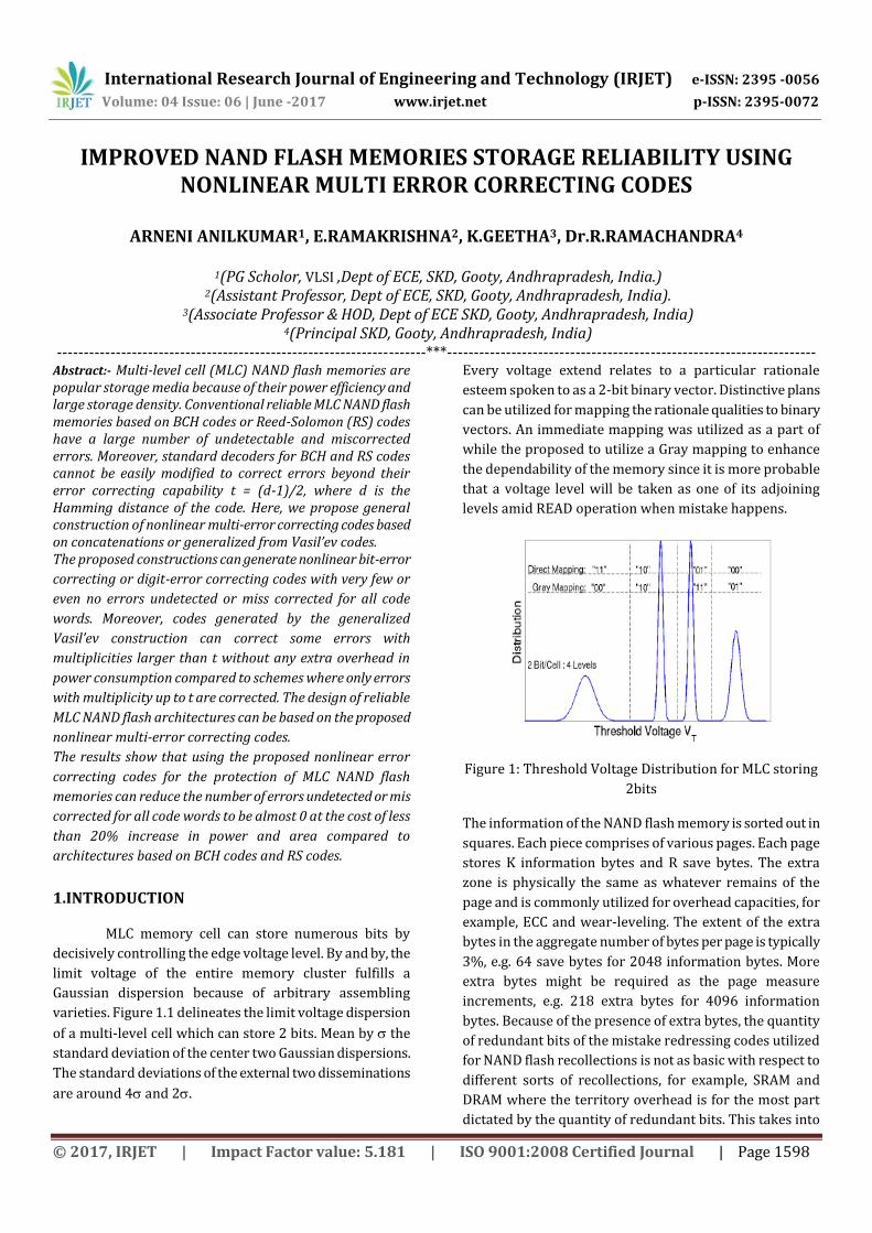
MLC memory cell can store numerous bits by
decisively controlling the edge voltage level. By and by, the
limit voltage of the entire memory cluster fulfills a
Gaussian dispersion because of arbitrary assembling
varieties. Figure 1.1 delineates the limit voltage dispersion
of a multi-level cell which can store 2 bits. Mean by the
standard deviation of the center two Gaussian dispersions.
The standard deviations of the external two disseminations
are around 4 and 2.
Every voltage extend relates to a particular rationale
esteem spoken to as a 2-bit binary vector. Distinctive plans
can be utilized for mapping the rationale qualities to binary
vectors. An immediate mapping was utilized as a part of
while the proposed to utilize a Gray mapping to enhance
the dependability of the memory since it is more probable
that a voltage level will be taken as one of its adjoining
levels amid READ operation when mistake happens.
Figure 1: Threshold Voltage Distribution for MLC storing
2bits
The information of the NAND flash memory is sorted out in
squares. Each piece comprises of various pages. Each page
stores K information bytes and R save bytes. The extra
zone is physically the same as whatever remains of the
page and is commonly utilized for overhead capacities, for
example, ECC and wear-leveling. The extent of the extra
bytes in the aggregate number of bytes per page is typically
3%, e.g. 64 save bytes for 2048 information bytes. More
extra bytes might be required as the page measure
increments, e.g. 218 extra bytes for 4096 information
bytes. Because of the presence of extra bytes, the quantity
of redundant bits of the mistake redressing codes utilized
for NAND flash recollections is not as basic with respect to
different sorts of recollections, for example, SRAM and
DRAM where the territory overhead is for the most part
dictated by the quantity of redundant bits. This takes into
International Research Journal of Engineering and Technology (IRJET) e-ISSN: 2395 -0056
Volume: 04 Issue: 06 | June -2017 www.irjet.net p-ISSN: 2395-0072
© 2017, IRJET | Impact Factor value: 5.181 | ISO 9001:2008 Certified Journal | Page 1599
account an adaptable plan of all the more intense blunder
rectifying codes for NAND flash recollections.
Memories Similar to SLC streak recollections, the essential
disappointment systems for MLC NAND streak
recollections incorporate limit voltage conveyance,
program/read exasperate, information maintenance,
programming/eradicating perseverance and single
occasion surprise. Be that as it may, while for SLC streak
recollections a considerable measure of mistakes are
uneven, e.g. blunders presented by program unsettling
influence and information maintenance, for MLC NAND
streak recollections mistakes have no favored symmetry.
Exploratory outcomes demonstrate that blunders in MLC
streak recollections will probably happen consistently
inside a page with no detectable burstiness or
neighborhood information reliance. Subsequently, all
through the paper we expect an arbitrary symmetric
blunder demonstrate, where P(e) = p||e||(1 − p)n−||e||, p is
the crude piece twisting rate and ||e|| is the assortment of
the mistake. we need to underline that the proposed
nonlinear t-mistake rectifying codes can likewise give an
ensured level of unwavering quality in circumstances
where the blunder model is erratic or multi-bit blunders
are more plausible.
With a specific end goal to exhibit the benefit of using least
separation incompletely vigorous code to secure memory
against delicate mistakes, we think about the blunder
recognition/revision properties and additionally the
equipment overhead of a (39, 32, 4) stretched out Vasil'ev
code to the alteration of a being used (39, 32, 4) broadened
Hamming code. To ensure twofold information rate DIMM
memory in a Virtex-II Pro device.
It portray the usefulness of the memory read and compose
operations, encoding the data, and finding the blunders of
recovered information to execute the calculation.
Amid a WRITE operation, the redundant bits of the code
are produced by the encoder and spared in the redundant
memory square. Amid a READ operation, the ECC square
processes the mark of the recovered information and
executes the mistake rectification calculation. In the event
that uncorrectable mistakes happen, ERR will be attested
and no remedy will be endeavored.
2. LITERATURE SURVEY
The expansion of the capacity thickness and the reduction
of the cost per bit of blaze recollections were traditionally
accomplished by the forceful scaling of the memory cell
transistor until the multilevel cell (MLC) innovation was
produced and executed in 1997. The semiconductor
business witnesses a touchy development of the NAND
streak memory showcase in the previous quite a long
while. Because of its high information exchange rate, low
power consumption, huge capacity thickness and long
mechanical strength, the NAND streak recollections are
broadly utilized as capacity media for gadgets, for example,
versatile media players, advanced cameras, cell phones and
low-end net books.
MLC innovation depends on the capacity to decisively
control the measure of charge put away into the drifting
door of the memory cell with the end goal of setting the
limit voltage to various diverse levels corresponding to
various rationale values, which empowers the capacity of
multiple bits per cell. Be that as it may, the expanded
number of programming limit voltage levels negatively
affects the dependability of the gadget because of the
diminished operational edge. The crude bit error rate of
the MLC NAND streak memory is around 10 and is no less
than two requests of size more regrettable than that of the
single-level cell (SLC) NAND streak memory.
Additionally, a similar unwavering quality concerns with
respect to SLC NAND streak recollections, e.g.,
program/read aggravate, information retention,
programming/deleting perseverance and delicate errors,
may spin out to be more huge for MLC NAND streak
recollections. Subsequently an intense error amending
code (ECC) that can redress no less than 4-bit errors is
required for the MLC NAND streak recollections to
accomplish an adequate application bit error rate, which is
no bigger than 10. A few works have explored the
utilization of direct piece codes to enhance the unwavering
quality of MLC NAND streak recollections. In, the creators
displayed a high-throughput and low-control ECC
architecture in view of BCH codes amending fourfold error.
In a 4Gb 2b/cell NAND streak memory chip joining a 250
MHz BCH error adjusting architecture was appeared. It
demonstrated that the utilization of strong BCH codes
(e.g.,12,15,67,102) can successfully build the quantity of
bits/cell hence additionally expanding the capacity limit of
MLC NAND streak recollections.
International Research Journal of Engineering and Technology (IRJET) e-ISSN: 2395 -0056
Volume: 04 Issue: 06 | June -2017 www.irjet.net p-ISSN: 2395-0072
© 2017, IRJET | Impact Factor value: 5.181 | ISO 9001:2008 Certified Journal | Page 1600
In a versatile rate ECC architecture in view of BCH codes
was proposed. The plan had four operation modes with
various error adjusting capacities. An ECC architecture in
light of Reed-Solomon (RS) codes of length 828 and 820
information digits constructed over was proposed, which
can adjust all bit errors of variety not exactly or equivalent
to four. The architecture accomplishes higher throughput,
requires less territory overhead for the encoder and the
decoder yet needs 32 more redundant bits than
architectures in light of BCH codes with a similar error
rectifying ability. In, an architecture in light of hilter kilter
restricted extent error redressing code was proposed,
which can amend every single deviated error of
multiplicities up to " t'. The above architectures depend on
straight square codes and have countless errors. For any
direct code with k information bits, the quantity of
imperceptible errors is 2K.
Recollections assume a vital part in today's system-on-chip
(SOC) plans. At the season of introduction of glimmer
memory 70% of the chip zone in a large portion of today's
processors is taken by installed memory and this number
is required to achieve 90% by 2011. As memory involves a
major rate of the region on a chip, it is particularly
powerless against single-event-upset (SEU) brought about
by single, enthusiastic particles like high-vitality neutrons
and alpha particles. SEU briefly changes the condition of
the gadgets and results in delicate errors, which are non-
damaging and show up as undesirable bit flips in memory
cells and registers. With continuous scaling, SEU spins out
to be more likely and the delicate error rate increments. As
the speed of the gadgets ends up noticeably higher the
relative size of the clock transition timing window expands,
which makes gadgets more touchy to SEU. The abatement
of connected voltage additionally raises the delicate error
rate since bit inversion will probably happen when the
electrical charge put away in the memory cell is low
because of reduction in the voltage.
Straight single error correction, double error detection
codes (SEC-DED) is utilized as a part of present day PC
systems as a countermeasure against delicate errors to
build the unwavering quality of the system. These codes
have Hamming separation 4 and can rectify all single bit
errors and identify all double bit errors. Within the sight of
multiple errors,the unwavering quality of systems using
error protection plans in view of direct codes might be
questionable. For any direct (n, k) SEC-DED error
amending codes, the quantity of imperceptible multiple
errors is 2k. In addition to this, an immense number of
multiple errors will be miscorrected as single bit errors. As
a rule SEU brings about multiple bit distortions, these
codes may not be adequate to accommodate a high
dependability.
Truth be told, abnormality of systems created by multiple
bit upset (MBU) was at that point detailed. It was
demonstrated that the Cassini Solid-State Recorder was
encountering a high rate of uncorrectable multiple bit
errors. It has concluded that the MBU rate was architecture
needy and any architecture of DRAM-based outlines must
be investigated deliberately to stay away from sudden high
MBU rate. The unwavering quality of systems secured by
two sorts of single error amending codes was analyzed.
The error rate was accounted for and it additionally
concluded that conventional ECC may not be adequate to
ensure gadgets against multiple bit errors for certain
configuration designs. The expansion of MBU rate in
profound submicron advancements break down the
situation much further. In 65nm triple-well SRAMs with a
thin cell architecture, the rate of multiple bit errors created
by neutron incited SEU increments by an element of 10
contrasted and that in 90nm innovations, almost 55% of
the errors because of neutron radiation were multiple bit
errors. In spite of the fact that there are instruments like
bit interleaving that can be utilized to limit the error rate
contribution of multiple bit errors, regardless of whether it
is sufficient under such high MBU rate is as yet obscure.
The upside of bit interleaving includes some significant
pitfalls of more format constrains, which may bring about
bigger power consumptions and longer get to times.
Subsequently, memory protection plans which can give
better protection against multiple bit errors than that in
light of traditional straight codes are popular. We propose
a system for plan of solid recollections in view of nonlinear
SEC-DED somewhat powerful codes. These codes have less
imperceptible errors and less multi bit errors which are
constantly miscorrected while requiring comparable
equipment overhead as the conventional direct SEC-DED
codes. We suggest that direct augmented Hamming codes
can be supplanted by nonlinear broadened Vasil'ev SEC-
DED codes bringing about enhanced unwavering quality
within the sight of multibit distortions. The error detection
pieces of various codes are thought about and the reason
why the broadened Vasil'ev code is chosen is clarified. The
architecture using broadened Vasil'ev codes is portrayed
and the error remedying calculation is appeared in detail.
The equipment overhead and error revising and
distinguishing properties of the augmented Vasil'ev code
International Research Journal of Engineering and Technology (IRJET) e-ISSN: 2395 -0056
Volume: 04 Issue: 06 | June -2017 www.irjet.net p-ISSN: 2395-0072
© 2017, IRJET | Impact Factor value: 5.181 | ISO 9001:2008 Certified Journal | Page 1601
are contrasted with the broadened Hamming codes with
demonstrate the upside of the proposed approach.
The Intel Strata Flash memory innovation speaks to a cost
achievement for glimmer memory gadgets by empowering
the capacity of two bits of information in a single blaze
memory transistor. This paper will examine the evolution
of the no-account/cell innovation from conception to
production. The glimmer memory business has developed
from about $50M in 1987 to generally $2.5B in 1997
because of its extraordinary blend of functionality and cost.
Flash memory gadgets are presently found in for all intents
and purposes each PC and cellular phone and are one of the
key components of the developing advanced imaging and
sound markets. Taken a toll for every bit reduction of blaze
memory gadgets has been traditionally accomplished by
forceful scaling of the memory cell transistor utilizing
silicon prepare scaling methods, for example,
photolithography line width reduction. While trying to
quicken the rate of cost reduction beyond that
accomplished by process scaling, an exploration program
was begun in 1992 to create strategies for the dependable
stockpiling of multiple bits of information in a single blaze
memory cell. The Intel Strata Flash no-account/cell
memory innovation is the principal yield of the multi-bit
per cell stockpiling exertion. By putting away two bits in a
single memory transistor, the memory cell range is viably
sliced down the middle permitting the capacity of twice as
much information in an indistinguishable territory from
the standard single bit per cell innovation. This gives
understanding into the Intel Strata Flash memory
innovation advancement exertion. It talks about the
evolution of the no-account/cell ability from conception to
production and the difficulties that were effectively
overcome to deliver an excellent item perfect with the
standard single bit per cell gadgets. This additionally
introduces cases that grandstand the advantages of the
current Intel Strata Flash memory gadgets and examines a
portion of the main impetuses for high thickness streak
memory.
NAND Flash memory items have spined into the innovation
of decision to fulfill high thickness, Non unstable memory
prerequisites in numerous applications. NAND Flash
innovation gives a lot of capacity at a value point lower
than any of today's semiconductor options. NAND Flash
advancement has concentrated on minimal effort per bit,
bringing about an innovation that requires fundamentally
more system association than other blaze advances.
Specifically, NAND Flash memory can be required to
experience minor information corruption sooner or later
amid ordinary operation.
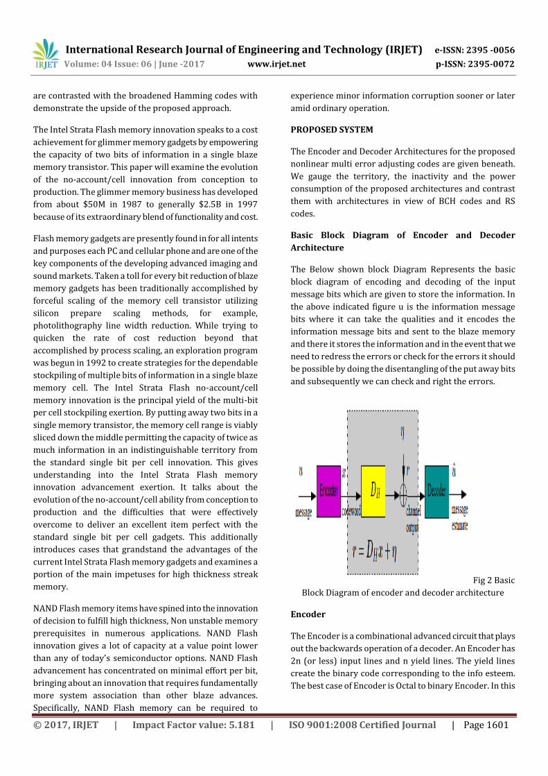
PROPOSED SYSTEM
The Encoder and Decoder Architectures for the proposed
nonlinear multi error adjusting codes are given beneath.
We gauge the territory, the inactivity and the power
consumption of the proposed architectures and contrast
them with architectures in view of BCH codes and RS
codes.
Basic Block Diagram of Encoder and Decoder
Architecture
The Below shown block Diagram Represents the basic
block diagram of encoding and decoding of the input
message bits which are given to store the information. In
the above indicated figure u is the information message
bits where it can take the qualities and it encodes the
information message bits and sent to the blaze memory
and there it stores the information and in the event that we
need to redress the errors or check for the errors it should
be possible by doing the disentangling of the put away bits
and subsequently we can check and right the errors.
Fig 2 Basic
Block Diagram of encoder and decoder architecture
Encoder
The Encoder is a combinational advanced circuit that plays
out the backwards operation of a decoder. An Encoder has
2n (or less) input lines and n yield lines. The yield lines
create the binary code corresponding to the info esteem.
The best case of Encoder is Octal to binary Encoder. In this
International Research Journal of Engineering and Technology (IRJET) e-ISSN: 2395 -0056
Volume: 04 Issue: 06 | June -2017 www.irjet.net p-ISSN: 2395-0072
© 2017, IRJET | Impact Factor value: 5.181 | ISO 9001:2008 Certified Journal | Page 1602
case the information sources are eight and the yield bits
are 3 which gives binary qualities.
NAND Flash Memory
NAND Flash gadgets utilize one of two diverse memory cell
innovations. The primary cell configuration is the
traditional implementation, where every memory cell
speaks to a single bit of information. The single-bit-per-cell
approach is arranged as single-level cell (SLC). The second
approach is to program every cell in incremental sums.
With this approach, the information esteem is dictated by
how "hard" a cell has been modified.
This multilevel cell (MLC) approach enables every cell to
speak to 2 bits of information. Verifiably, SLC NAND Flash
gadgets have given enhanced information trustworthiness
when contrasted and their MLC partners. The information
respectability in MLC requires a significantly more modern
error correction plot than is utilized for SLC NAND Flash
gadgets.
This specialized note depicts the utilization of
straightforward Hamming codes to identify and adjust
information corruption that happens amid ordinary SLC
NAND Flash gadget operation. The Hamming calculation is
fit for repairing single-bit information disappointments
and distinguishing whether 2 bits have spined out to be
adulterated. The Hamming calculation is an industry
acknowledged technique for error detection and correction
in numerous SLC NAND Flash-based applications
Decoder
A binary code of n bits is fit for speaking to up to
2n unmistakable components of the coded information. A
decoder is a combinational circuit that converts binary
information from the n coded contributions to a most
extreme of 2n remarkable yields. On the off chance that the
n bit coded information has unused bit combinations, the
decoder may have under 2n yields. The Decoder exhibited
here are called n to m line decoders, where m<n.
Encoder Architecture
The encoders for straight BCH codes and RS codes are
conventionally actualized in light of direct criticism enlist
(LFSR) architecture. Both the serial and the parallel
architectures for LFSRs are very much contemplated in the
group. When all is said in done, the serial LFSR needs k
clock cycles while the parallel LFSR needs only (k/q) clock
cycles to complete the computation of the redundant bits at
the cost of higher equipment multifaceted nature, where k
is the quantity of information bits and q is the parallelism
level of the LFSRs. Contrasted with the encoder for straight
BCH codes, the encoder for the proposed nonlinear t error
adjusting code fundamentally requires one more multiplier
in GF(2r2)and two r2 registers.
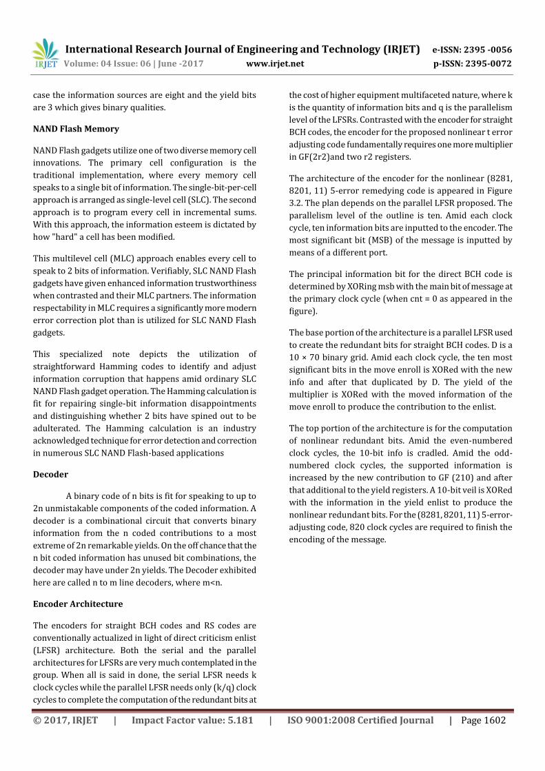
The architecture of the encoder for the nonlinear (8281,
8201, 11) 5-error remedying code is appeared in Figure
3.2. The plan depends on the parallel LFSR proposed. The
parallelism level of the outline is ten. Amid each clock
cycle, ten information bits are inputted to the encoder. The
most significant bit (MSB) of the message is inputted by
means of a different port.
The principal information bit for the direct BCH code is
determined by XORing msb with the main bit of message at
the primary clock cycle (when cnt = 0 as appeared in the
figure).
The base portion of the architecture is a parallel LFSR used
to create the redundant bits for straight BCH codes. D is a
10 × 70 binary grid. Amid each clock cycle, the ten most
significant bits in the move enroll is XORed with the new
info and after that duplicated by D. The yield of the
multiplier is XORed with the moved information of the
move enroll to produce the contribution to the enlist.
The top portion of the architecture is for the computation
of nonlinear redundant bits. Amid the even-numbered
clock cycles, the 10-bit info is cradled. Amid the odd-
numbered clock cycles, the supported information is
increased by the new contribution to GF (210) and after
that additional to the yield registers. A 10-bit veil is XORed
with the information in the yield enlist to produce the
nonlinear redundant bits. For the (8281, 8201, 11) 5-error-
adjusting code, 820 clock cycles are required to finish the
encoding of the message.
International Research Journal of Engineering and Technology (IRJET) e-ISSN: 2395 -0056
Volume: 04 Issue: 06 | June -2017 www.irjet.net p-ISSN: 2395-0072
© 2017, IRJET | Impact Factor value: 5.181 | ISO 9001:2008 Certified Journal | Page 1603
Figure 3: Encoder Architecture for nonlinear 5 ECC
Decoder Architecture
The decoding of the nonlinear t-error-revising codes
requires the interpreting of a direct BCH code with one less
information bits. The standard decoder for the direct BCH
codes for the most part contains three sections: the
disorder computation hinder, the error locator polynomial
generation piece and the Chien seek square. The Decoder
square of BCH code requires only four pieces and the
Decoder hinder for RS code requires an additional piece
and absolutely it requires five squares. Give us access
insight about the each piece for both BCH codes and RS
codes.
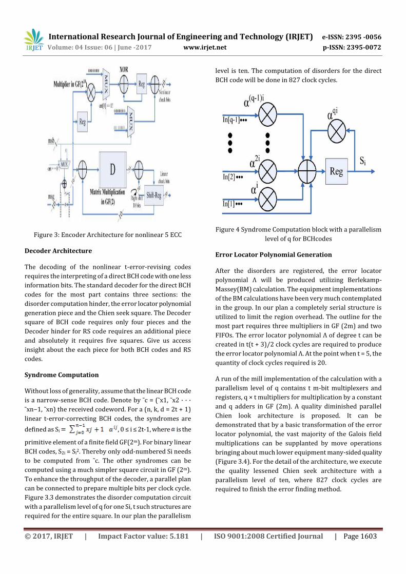
Syndrome Computation
Without loss of generality, assume that the linear BCH code
is a narrow-sense BCH code. Denote by ˜c = (˜x1, ˜x2 · · ·
˜xn−1, ˜xn) the received codeword. For a (n, k, d = 2t + 1)
linear t-error-correcting BCH codes, the syndromes are
defined as Si , 0 ≤ i ≤ 2t-1, where is the
primitive element of a finite field GF(2m). For binary linear
BCH codes, S2i = Si2. Thereby only odd-numbered Si needs
to be computed from ˜c. The other syndromes can be
computed using a much simpler square circuit in GF (2m).
To enhance the throughput of the decoder, a parallel plan
can be connected to prepare multiple bits per clock cycle.
Figure 3.3 demonstrates the disorder computation circuit
with a parallelism level of q for one Si, t such structures are
required for the entire square. In our plan the parallelism
level is ten. The computation of disorders for the direct
BCH code will be done in 827 clock cycles.
Figure 4 Syndrome Computation block with a parallelism
level of q for BCHcodes
Error Locator Polynomial Generation
After the disorders are registered, the error locator
polynomial Λ will be produced utilizing Berlekamp-
Massey(BM) calculation. The equipment implementations
of the BM calculations have been very much contemplated
in the group. In our plan a completely serial structure is
utilized to limit the region overhead. The outline for the
most part requires three multipliers in GF (2m) and two
FIFOs. The error locator polynomial Λ of degree t can be
created in t(t + 3)/2 clock cycles are required to produce
the error locator polynomial Λ. At the point when t = 5, the
quantity of clock cycles required is 20.
A run of the mill implementation of the calculation with a
parallelism level of q contains t m-bit multiplexers and
registers, q × t multipliers for multiplication by a constant
and q adders in GF (2m). A quality diminished parallel
Chien look architecture is proposed. It can be
demonstrated that by a basic transformation of the error
locator polynomial, the vast majority of the Galois field
multiplications can be supplanted by move operations
bringing about much lower equipment many-sided quality
(Figure 3.4). For the detail of the architecture, we execute
the quality lessened Chien seek architecture with a
parallelism level of ten, where 827 clock cycles are
required to finish the error finding method.
International Research Journal of Engineering and Technology (IRJET) e-ISSN: 2395 -0056
Volume: 04 Issue: 06 | June -2017 www.irjet.net p-ISSN: 2395-0072
© 2017, IRJET | Impact Factor value: 5.181 | ISO 9001:2008 Certified Journal | Page 1604
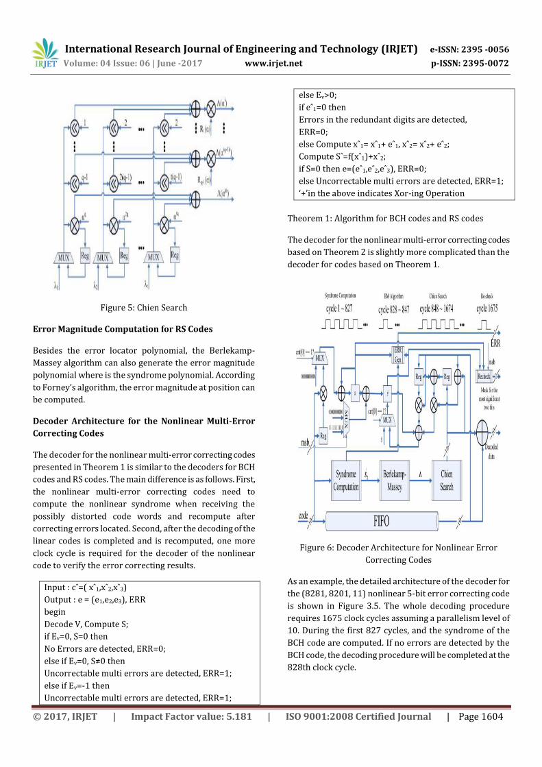
Figure 5: Chien Search
Error Magnitude Computation for RS Codes
Besides the error locator polynomial, the Berlekamp-
Massey algorithm can also generate the error magnitude
polynomial where is the syndrome polynomial. According
to Forney’s algorithm, the error magnitude at position can
be computed.
Decoder Architecture for the Nonlinear Multi-Error
Correcting Codes
The decoder for the nonlinear multi-error correcting codes
presented in Theorem 1 is similar to the decoders for BCH
codes and RS codes. The main difference is as follows. First,
the nonlinear multi-error correcting codes need to
compute the nonlinear syndrome when receiving the
possibly distorted code words and recompute after
correcting errors located. Second, after the decoding of the
linear codes is completed and is recomputed, one more
clock cycle is required for the decoder of the nonlinear
code to verify the error correcting results.
Input : cˆ=( xˆ1,xˆ2,xˆ3)
Output : e = (e1,e2,e3), ERR
begin
Decode V, Compute S;
if Ev=0, S=0 then
No Errors are detected, ERR=0;
else if Ev=0, S≠0 then
Uncorrectable multi errors are detected, ERR=1;
else if Ev=-1 then
Uncorrectable multi errors are detected, ERR=1;
else Ev>0;
if eˆ1=0 then
Errors in the redundant digits are detected,
ERR=0;
else Compute xˆ1= xˆ1+ eˆ1, xˆ2= xˆ2+ eˆ2;
Compute Sˆ=f(xˆ1)+xˆ2;
if S=0 then e=(eˆ1,eˆ2,eˆ3), ERR=0;
else Uncorrectable multi errors are detected, ERR=1;
‘+’in the above indicates Xor-ing Operation
Theorem 1: Algorithm for BCH codes and RS codes
The decoder for the nonlinear multi-error correcting codes
based on Theorem 2 is slightly more complicated than the
decoder for codes based on Theorem 1.
Figure 6: Decoder Architecture for Nonlinear Error
Correcting Codes
As an example, the detailed architecture of the decoder for
the (8281, 8201, 11) nonlinear 5-bit error correcting code
is shown in Figure 3.5. The whole decoding procedure
requires 1675 clock cycles assuming a parallelism level of
10. During the first 827 cycles, and the syndrome of the
BCH code are computed. If no errors are detected by the
BCH code, the decoding procedure will be completed at the
828th clock cycle.
International Research Journal of Engineering and Technology (IRJET) e-ISSN: 2395 -0056
Volume: 04 Issue: 06 | June -2017 www.irjet.net p-ISSN: 2395-0072
© 2017, IRJET | Impact Factor value: 5.181 | ISO 9001:2008 Certified Journal | Page 1605
Input : cˆ=( xˆ1,xˆ2,xˆ3)
Output : e = (e1,e2,e3), ERR
begin Decode V, Compute eˆ2, Ev, S;
if Ev=0, S=0 then
No Errors are detected, ERR=0;
else if Ev=0, S≠0 then if d=3 then
Errors either occur only in the redundant bits are
uncorrectable multi-errors;
ERR=1;
else Decode U, compute eˆ1, eˆ3,Ev;
if Ev>0 then e=(eˆ1,(β( eˆ1),0), eˆ3);
e will only be corrected when ||e||≤t;
ERR=0 when errors are corrected and ERR=1 otherwise;
else
Uncorrectable multi errors are detected, ERR=1;
else if Ev=-1 then
Uncorrectable multi errors are detected, ERR=1;
else Ev is larger than 0;
Compute:;
xˆ2= xˆ2+ eˆ2;
vˆ=(β( xˆ1),0)+ xˆ2);
xˆ3= xˆ3+f(vˆk) (vˆk is the information part of vˆ);
Decode U according to xˆ1 and xˆ3;
If Ev=0 then
e=(0, eˆ2,0);
e will be only corrected if there are errors in the
information bits;
ERR=0 when errors are corrected and ERR=1 otherwise;
else if Ev>0 then
e=(eˆ1,(β( eˆ1),0)+ eˆ2 ,eˆ3);
e will only be corrected when ||e||≤t and there are
errors in the information bits;
ERR=0 when errors are corrected and ERR=1 otherwise;
else Ev=-1, uncorrectable multi errors are detected,
ERR=1;
‘+’in the above indicates Xor-ing Operation
Theorem 2: Algorithm for Nonlinear Block codes
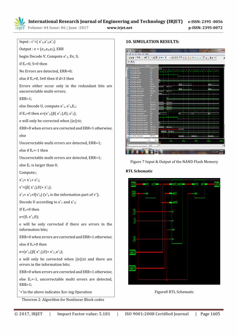
10. SIMULATION RESULTS:
Figure 7 Input & Output of the NAND Flash Memory
RTL Schematic
Figure8 RTL Schematic
International Research Journal of Engineering and Technology (IRJET) e-ISSN: 2395 -0056
Volume: 04 Issue: 06 | June -2017 www.irjet.net p-ISSN: 2395-0072
© 2017, IRJET | Impact Factor value: 5.181 | ISO 9001:2008 Certified Journal | Page 1606
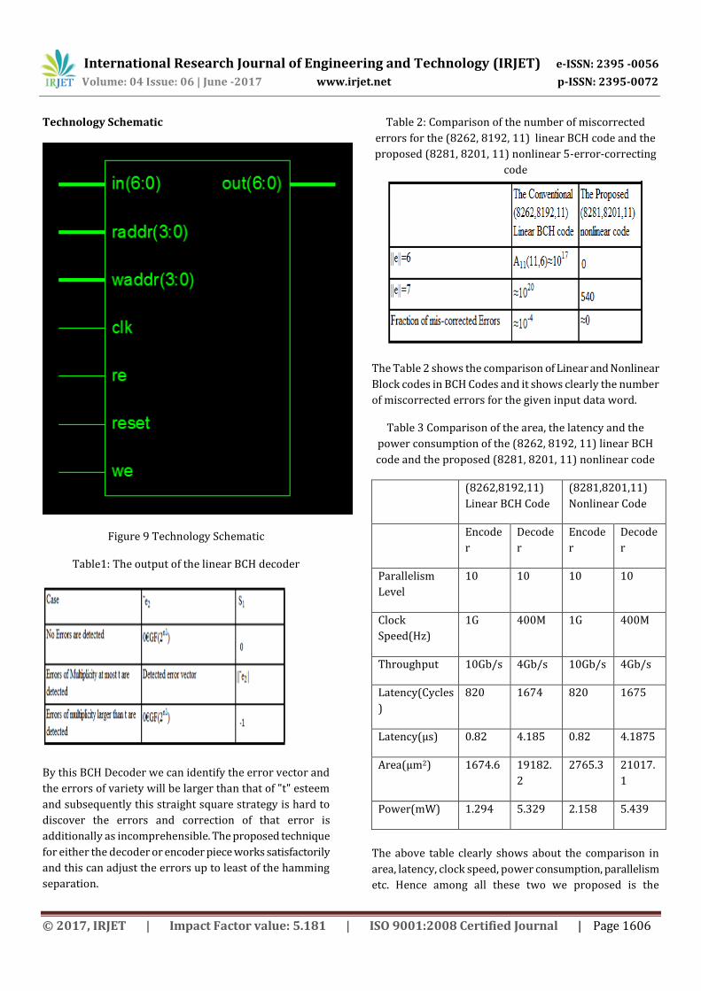
Technology Schematic
Figure 9 Technology Schematic
Table1: The output of the linear BCH decoder
By this BCH Decoder we can identify the error vector and
the errors of variety will be larger than that of "t" esteem
and subsequently this straight square strategy is hard to
discover the errors and correction of that error is
additionally as incomprehensible. The proposed technique
for either the decoder or encoder piece works satisfactorily
and this can adjust the errors up to least of the hamming
separation.
Table 2: Comparison of the number of miscorrected
errors for the (8262, 8192, 11) linear BCH code and the
proposed (8281, 8201, 11) nonlinear 5-error-correcting
code
The Table 2 shows the comparison of Linear and Nonlinear
Block codes in BCH Codes and it shows clearly the number
of miscorrected errors for the given input data word.
Table 3 Comparison of the area, the latency and the
power consumption of the (8262, 8192, 11) linear BCH
code and the proposed (8281, 8201, 11) nonlinear code
(8262,8192,11)
Linear BCH Code
(8281,8201,11)
Nonlinear Code
Encode
r
Decode
r
Encode
r
Decode
r
Parallelism
Level
10 10 10 10
Clock
Speed(Hz)
1G 400M 1G 400M
Throughput 10Gb/s 4Gb/s 10Gb/s 4Gb/s
Latency(Cycles
)
820 1674 820 1675
Latency(µs) 0.82 4.185 0.82 4.1875
Area(µm2) 1674.6 19182.
2
2765.3 21017.
1
Power(mW) 1.294 5.329 2.158 5.439
The above table clearly shows about the comparison in
area, latency, clock speed, power consumption, parallelism
etc. Hence among all these two we proposed is the
International Research Journal of Engineering and Technology (IRJET) e-ISSN: 2395 -0056
Volume: 04 Issue: 06 | June -2017 www.irjet.net p-ISSN: 2395-0072
© 2017, IRJET | Impact Factor value: 5.181 | ISO 9001:2008 Certified Journal | Page 1607
nonlinear block codes which can detect the 5 errors and
correct up to 5 errors.
Timing Summary
Speed Grade: -4
Minimum period: 5.014ns (Maximum Frequency:
199.442MHz)
Minimum input arrival time before clock: 7.742ns
Maximum output required time after clock: 4.368ns
CONCLUSION
The constructions of two nonlinear multi-error revising
codes are proposed. Their error redressing calculations are
introduced. The proposed codes have a great deal less
imperceptible and miscorrected errors than the
conventional BCH codes and RS codes. The code
constructed can likewise revise a few errors with
assortment larger than its error amending ability with no
additional overhead in zone, timing, and power
consumption contrasted with plans that right only up to
errors. The beyond-error redressing capacity of the
displayed nonlinear multi-error amending codes brings
about a further change of the unwavering quality of the
system.
FUTURE SCOPE
The plans of solid MLC NAND streak recollections in view
of the proposed nonlinear multi-error amending codes are
exhibited. We look at the territory, the inertness and the
power consumption of the dependable MLC NAND streak
architectures utilizing the proposed nonlinear multi-error
adjusting codes to architectures in view of BCH codes and
RS codes. The encoder and the decoder for every one of the
choices are displayed in Verilog and blended in RTL Design
Compiler. The outcomes demonstrate that architectures in
light of nonlinear multi-error amending codes can have
near zero imperceptible and miscorrected errors while
consuming under 20% more zone and power consumption
than architectures in light of the BCH codes and the RS
codes.
REFERENCES
1. G. Atwood, A. Fazio, D. Mills, and B. Reaves, “Intel
Strata Flash TM memory technology overview,” Intel
Technology Journal, 1997.
2. J.Cooke, “The inconvenient truths about NAND flash
memory,” Micron MEMCON’07 presentation, 2007.
3. R. Dan and R. Singer, “White paper: Implementing MLC
NAND flash for cost-effective, high capacity memory,”
M-Systems, 2003.
4. R. Bez, E. Camerlenghi, A. Modelli, and A.
Visconti,“Introduction to flash memory,” Proceedings
of the IEEE, vol. 91, no. 4, pp. 489–502, April 2003.
5. G. Cellere, S. Gerardin, M. Bagatin, A. Paccagnella, A.
Visconti, M. Bonanomi, S. Beltrami, R. Harboe-
Sorensen, A. Virtanen, and P. Roche, “Can atmospheric
neutrons induce soft errors in NAND floating gate
memories?” Electron Device Letters, IEEE, vol. 30, no.
2, pp. 178–180, Feb. 2009.
6. M. Bagatin, G. Cellere, S. Gerardin, A. Paccagnella, VA.
Visconti, S. Beltrami,Vand M. Maccarrone, “Single event
effects in 1Gbit 90nm NAND flash memories under
operating conditions,” in On-Line Testing Symposium,
2007. IOLTS 07. 13th IEEE International, July 2007, pp.
146–151.
7. F. Irom and D. Nguyen, “Single event effect
characterization of high density commercial NAND and
NOR nonvolatile flash memories,” Nuclear Science,
IEEE Transactions on, vol. 54, no. 6, pp. 2547–2553,
Dec.2007.
8. W. Liu, J. Rho, and W. Sung, “Low-power high
throughput BCH error correction VLSI design formulti-
level cell NAND flash memories,” in Signal Processing
Systems Design and Implementation,2006. SIPS ’06.
IEEE Workshop on, Oct. 2006, pp.303–308.
9. R. Micheloni, R. Ravasio, A. Marelli, E. Alice,V. Altieri, A.
Bovino, L. Crippa, E. Di Martino,L. D’Onofrio, A.
Gambardella, E. Grillea, G. Guerra,D. Kim, C. Missiroli, I.
Motta, A. Prisco, G. Ra one,M. Romano, M. Sangalli, P.
Sauro, M. Scotti, and S. Won, “A 4Gb 2b/cell NAND
flash memory with embedded 5b BCH ECC for 36mb/s
system read throughput,” in Solid-State Circuits
Conference, 2006.ISSCC 2006. Digest of Technical
Papers. IEEE International, Feb. 2006, pp. 497–506.
10. F. Sun, S. Devarajan, K. Rose, and T. Zhang, “Designof
on-chip error correction systems for multilevelNOR
and NAND flash memories,” IET Circuits, Devicesand
Systems, vol. 1, no. 3, pp. 241–249, 2007.
11. T.H. Chen, Y.Y.Hsiao, Y.T.Hsing, and C.W.Wu,“An
adaptive-rate error correction scheme for NAND flash
memory,” in VLSI Test Symposium, 2009.VTS’09. 27th
IEEE, May 2009, pp. 53–58.
12. B. Chen, X. Zhang, and Z. Wang, “Error correction for
multi-level NAND flash memory using Reed-Solomon
International Research Journal of Engineering and Technology (IRJET) e-ISSN: 2395 -0056
Volume: 04 Issue: 06 | June -2017 www.irjet.net p-ISSN: 2395-0072
© 2017, IRJET | Impact Factor value: 5.181 | ISO 9001:2008 Certified Journal | Page 1608
codes,” in Signal Processing Systems, 2008.SiPS 2008.
IEEE Workshop on, Oct. 2008, pp. 94–99
13. Y. Cassuto, M. Schwartz, V. Bohossian, and J. Bruck,
“Codes for multi-level flash memories: Correcting
asymmetric limited-magnitude errors,” in Information
Theory, 2007. ISIT 2007. IEEE International Symposium
on, June 2007, pp. 1176–1180.
AUTHORS:
1. ARNENI ANILKUMAR.
He completed his professional career of
education in B.Tech (ECE) at Sri
Krishnadevaraya engineering college,
Gooty and pursuing M.Tech from Sri
Krishnadevaraya engineering college,
Gooty, Anantapur(AP).He is interested
in VLSI
2. E.RAMAKRISHNA has 4 years
experience in teaching in graduate and
post graduate level and she presently
working as Assistant professor in
department of ECE Sri Krishnadevaraya
Engineering College, Gooty, AP, India.
3. Ms.K.GEETHA has completed his
professional career of education in
B.Tech (ECE) from JNTU Anantapur. He
obtained M.Tech degree from
BITM,Ballary.. At present working as an
Associate Professor and Head of the ECE
Department in Sri Krishnadevaraya Engineering College,
Gooty of Anantapuramu district (AP).
4. Dr.R.RAMACHANDRA has completed
his professional career of education in
B.Tech (MECHANICAL) from JNTU
Hyderabad. He obtained M.Tech degree
from JNTU, Hyderabad. He obtained Phd
degree from JNTU, Hyderabad At present
working as Principal in Sri
Krishnadevaraya Engineering College, Gooty of
Anantapuramu district (AP).