static voltage stabilizer · international research journal of engineering and technology (irjet)...
TRANSCRIPT

International Research Journal of Engineering and Technology (IRJET) e-ISSN: 2395-0056
Volume: 05 Issue: 01 | Jan-2018 www.irjet.net p-ISSN: 2395-0072
© 2018, IRJET | Impact Factor value: 6.171 | ISO 9001:2008 Certified Journal | Page 86
Static Voltage Stabilizer
Kapil Mulchandani1, Shubham Bannore1, Shilpa Lambor2, Vrinda Parkhi2, Vikrant Bhalerao3
1Electronics, Vishwakarma Institute of Technology, Pune, India 2 Professor, Dept. of Electronics, Vishwakarma Institute of Technology, Pune, India
3Senior Design Manager, Aarcchor Innovations Pvt. Ltd., Pune India ---------------------------------------------------------------------***---------------------------------------------------------------------
Abstract - The forgoing stage of voltage stabilizer used in industries or for household is Servo Voltage Stabilizer. Commercially the approved range of their operation is 150V-240V or 90V-280V. Servo Voltage Stabilizer are also manufactured and used widely in spite of the fact that they are obsolete and use outdated technology. The lately introduced technology which excludes this old-fangled, low voltage, high correction time, high maintenance issues of servo stabilizer is Static Voltage Stabilizer (SVS). Static Voltage Stabilizer doesn’t include any moving parts as in servo voltage stabilizer. The voltage in SVS is produced with the assistance of electronic circuits also it has absolute electronics to achieve correction in voltages and time. Therefore, it has extremely high voltage correction speed than servo voltage stabilizer. The paper deals with the static voltage stabilizer which is controlled by TMS320F28069 a DSP based controller and a voltage changes are accounted with the help of Buck-Boost Transformer. Key Words: F28069, Power Electronics, Stabilizer, Static Voltage Stabilizer
1. INTRODUCTION
Stabilizers is an electronic device that stabilize the voltage from fickle to a desired value. Stabilizer provides a steady and secure power supply to equipment’s, which needs a stable voltage and also protects devices from most of the problems of the mains. As in UPS, voltage stabilizers also have proved an asset to the protection of electronic devices. The major utility of a stabilizer is to make the output voltage that feeds the equipment’s connected to it as much as possible equivalent to the ideal electrical power supply, ensuring that the oscillations in electrical power are offset, and its output maintain a stable value, precluding them from being experienced by equipment’s and thereby avoiding their damage. The disparity in stabilizer and regulator is voltage regulator is normally used in DC applications and voltage stabilizer on other hand is equipment that ’stabilizes’ the AC voltage which is usually fluctuating.
Fig -1. Block Diagram of Stabilizer
Voltage stabilizer can be broadly categorized as AC voltage stabilizer, DC voltage stabilizer and Automatic voltage stabilizer. This paper deals with Static voltage, an ac voltage stabilizer. The most used stabilizer is servo stabilizer and has many limitations in accordance with static voltage stabilizer.
2. STATIC VOLTAGE STABILIZER
The static voltage stabilizers proffer improvement on slow servo controlled stabilizer. The basic study of SVR is with buck-boost transformer with high primary to secondary ratio for voltage correction of 25%. The control voltage which is fed by the IGBT drives of SVS is given to the primary and input voltage is imposed to the secondary of the buck boost transformer. The regulation of voltage with help of buck and boost is attained electronically without any step changes in the voltage at the time when system regulates. This task is proficient through a feedback and a control system implemented by using a TMS320F28069 microcontroller. The system uses IGBTs as power switches, direct AC-AC converter circuit improves the overall system response and fast voltage correction. Also 12.8 KHz ePWM control operation using high end Piccolo F28069 control card to achieve correction time of 20 to 30 millisecond.
Fig -2. Block Diagram of Static Voltage Stabilizer
2.1. Major components of SVR
1. Buck Boost Transformer: Secondary of Buck and boost transformer is connected input and output terminal of voltage stabilizer. Neutral between input and output of static voltage stabilizer is common hence voltage induced across secondary of buck boost transformer can add or subtract with input voltage. Primary of buck boost transformer is connected to IGBT power stage.
International Research Journal of Engineering and Technology (IRJET) e-ISSN: 2395-0056
Volume: 05 Issue: 01 | Jan-2018 www.irjet.net p-ISSN: 2395-0072
© 2018, IRJET | Impact Factor value: 6.171 | ISO 9001:2008 Certified Journal | Page 87
2. IGBT Power Stage: It consists of IGBT Bridge which is connected to Piccolo F28069 DSP controller. IGBT power stage is responsible for the generation of appropriate amount of voltage with help of PWM method. The output of the IGBT power stage is fed to the primary as it is the control circuit of the device. As the output of the IGBTs is fed to the primary of the transformer, it can be in phase or 180 degrees out of phase with the input line voltages. So the voltage induced across the secondary of Buck-Boost Transformer can be added or subtracted as per the required voltage needed at the load.
3. DSP based Control board: The major work of the DSP based control board is to give PWM to drive the IGBT. It incessantly senses value of input voltage, output voltage, load current and IGBT current with help of current transformer and voltage transformer connected to it. And this processed information as in feedback gives signal to IGBT power stage to generate desired voltage and duty cycle with help of PWM method.
3. PICCOLO TMS320F28069
The F2806x Piccolo (Fig.3) family of microcontrollers (MCUs) provides the power of the C28x core and CLA coupled with highly integrated control peripherals in low pin count devices. This family is code-compatible with previous C28x-based code, and also provides a high level of analog integration. An internal voltage regulator allows for single rail operation. Enhancements have been made to the High-resolution Pulse Width Modulator (HRPWM) module to allow for dual-edge control (frequency modulation). Analog comparators with internal 12-bit references have been added and can be routed directly to control the ePWM outputs. The ADC converts from 0 to 3.3-V fixed full-scale range and supports ratio-metric VREFHI/VREFLO references. The ADC interface has been optimized for low overhead and latency. Features:
High-Efficiency 32-Bit CPU (TMS320C28x).
90 MHz (11.11-ns Cycle Time).
Harvard Bus Architecture.
Programmable Control Law Accelerator (CLA).
Embedded Memory Up to 256KB of Flash, Up to 100KB of RAM, 2KB of One-Time Programmable (OTP) ROM • Three 32-Bit CPU Timers.
Up to 8 Enhanced Pulse-Width Modulator (ePWM) Modules.
12-Bit Analog-to-Digital Converter (ADC), Dual Sample and-Hold (S/H).
Up to 54 Individually Programmable, Multiplexed General-Purpose Input/output (GPIO) Pins With Input
Filtering.
Code-Efficient (in C/C++ and Assembly).
4. PWM GENERATION
Pulse Width Modulation (PWM) is the method to produce variable voltages using digital means. Typically, variable voltages come from analog circuits and digital circuits that
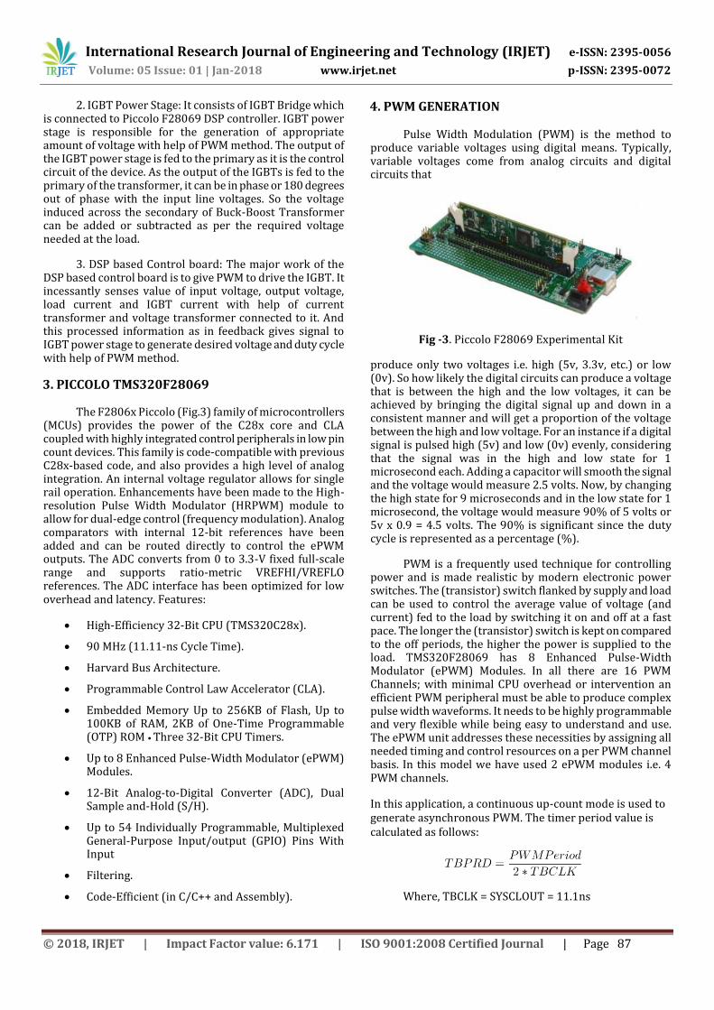
Fig -3. Piccolo F28069 Experimental Kit
produce only two voltages i.e. high (5v, 3.3v, etc.) or low (0v). So how likely the digital circuits can produce a voltage that is between the high and the low voltages, it can be achieved by bringing the digital signal up and down in a consistent manner and will get a proportion of the voltage between the high and low voltage. For an instance if a digital signal is pulsed high (5v) and low (0v) evenly, considering that the signal was in the high and low state for 1 microsecond each. Adding a capacitor will smooth the signal and the voltage would measure 2.5 volts. Now, by changing the high state for 9 microseconds and in the low state for 1 microsecond, the voltage would measure 90% of 5 volts or 5v x 0.9 = 4.5 volts. The 90% is significant since the duty cycle is represented as a percentage (%).
PWM is a frequently used technique for controlling power and is made realistic by modern electronic power switches. The (transistor) switch flanked by supply and load can be used to control the average value of voltage (and current) fed to the load by switching it on and off at a fast pace. The longer the (transistor) switch is kept on compared to the off periods, the higher the power is supplied to the load. TMS320F28069 has 8 Enhanced Pulse-Width Modulator (ePWM) Modules. In all there are 16 PWM Channels; with minimal CPU overhead or intervention an efficient PWM peripheral must be able to produce complex pulse width waveforms. It needs to be highly programmable and very flexible while being easy to understand and use. The ePWM unit addresses these necessities by assigning all needed timing and control resources on a per PWM channel basis. In this model we have used 2 ePWM modules i.e. 4 PWM channels.
In this application, a continuous up-count mode is used to generate asynchronous PWM. The timer period value is calculated as follows:
Where, TBCLK = SYSCLOUT = 11.1ns

International Research Journal of Engineering and Technology (IRJET) e-ISSN: 2395-0056
Volume: 05 Issue: 01 | Jan-2018 www.irjet.net p-ISSN: 2395-0072
© 2018, IRJET | Impact Factor value: 6.171 | ISO 9001:2008 Certified Journal | Page 88
Fig -4. Two Complementary PWM waves.
In many power electronics applications like Stabilizer, Inverter it is necessary that the turn-on periods of the two switches must not overlap with each other in order to avoid a shoot-through fault. Thus, a pair of non-overlapping PWM output is frequently required to properly turn on and off the two switches. A dead time (dead-band) is habitually inserted between the turning-off of one transistor along with the turning- on of the other transistor. This delay allows complete turning-off of one transistor before the turning - on of the other transistor. In F28069 Dead Band (DB) submodule takes care of it and generate the dead band desired by the user. In this application a dead band of 2 microseconds is generated.
Fig -5. Dead band of 2us Between Two PWM’s.
5. WORKING AND ANALYSIS OF SVS
Static Voltage Stabilizer is implemented on Piccolo F28069 DSP based board. This control board continuously senses input voltage, output voltage, load current and IGBT current with help of CTs and VTs. Based on these values Piccolo F28069 DSP control board will trigger IGBT Bridge to produce voltage at its output with help of PWM method. The details of operation of Static voltage regulator in Buck and Boost mode is mentioned below
5.1. Boost Mode
For explaining Boost Mode consider an example, for a load of 50kVA, 220V is connected at output of static voltage stabilizer and suppose low voltage of 180V is available at input line which needs to be corrected to 220V. When
Piccolo F28069 DSP control board senses values of input voltage, output voltage, load current and IGBT current, to correct voltage it will trigger IGBT bridge to generate 40V (220-180=40V) at its output which is in phase with input line voltages. It persuades 40V at secondary of buck boost transformer since both voltage; input line and voltage across secondary of buck boost transformer are in phase with each other , it get added and the output voltage get corrected to 220V.
Fig -6. Boost Mode Operation.
5.1.1. Analysis
Fig -7. Circuit Diagram of single phase SVR.
Vout = Vin + [Vind(1 −d)Vin]n = Vin[1 + (2d− 1)n]
The output voltage, Vout is the sum of the input voltage, Vin and the transformer voltage which is chopped AC voltage [= n (2d− 1)Vin]. n is the transformer ratio, d is the duty cycle. For switching frequency large compared to line frequency, we can write,
IAv-Q21 = (1/2π) {0∫(π-φ) d Ip sin ωt dωt + (π-φ)∫π (1-d) Ip sin ωt dωt}
= (Ip / 2π) {1 – cos φ + 2d cos φ} IRMS-Q21
2 = (1/2π) {0∫(π-φ) d2 Ip2 sin2 ωt dωt
+ (π- φ)∫π (1-d)2 Ip2 sin2 ωt dωt}
= (Ip
2 / 4π) {d2π+(1 – 2d)[φ + sin (2φ)/2]} From the above, we can write,

International Research Journal of Engineering and Technology (IRJET) e-ISSN: 2395-0056
Volume: 05 Issue: 01 | Jan-2018 www.irjet.net p-ISSN: 2395-0072
© 2018, IRJET | Impact Factor value: 6.171 | ISO 9001:2008 Certified Journal | Page 89
IAv-D21 = (Ip/π) - IAv-Q21
IRMS-D212 = Ip2/4 - IRMS-Q21
2
5.2. Buck Mode
Taking same example into consideration for a load of 50kVA, suppose high voltage of 250V is available at input line which needs to be corrected to 220V. Whenever Piccolo F28069 DSP control board measures values of input and output voltage, load current and IGBT current, to correct voltage it will trigger IGBT bridge to produce 30V (250220=30V) at its output which is 180 degree out of phase with input line voltages. It induces 30V at secondary of buck boost transformer; input line and voltage across secondary of buck boost transformer are 180 degree out of phase with each other and so it gets subtracted and output voltage is corrected to 220v.
This increase or decrease in voltage according to the rated voltage the Buck and Boost mode take place and the desired output is observed.
Fig -8. Buck Mode Operation.
6. SIMULATION
Below Figure shows the simulation model for open loop Static Voltage Stabilizer. For rectification of AC input, 4 diodes are used and the rectified output is fed to IGBTs. In this model 4 IGBTs are used which are driven using the pulse generator. Two IGBTs get the same drive i.e. the positive or negative pulse. The output of the IGBTs is given to the primary of the Transformer. And subsequently transformer is connected to load.
Fig -9. Simulink Simulation Model
Fig -10. Simulink Simulation Result
7. HARDWARE DESCRIPTION
The below figure illustrate DSP controlled KVA single phase Static Voltage Stabilizer. The research was carried on Piccolo F28069 (DSP) kit, IGBT driver circuit, rectifier circuit, Buck-Boost Transformer and DSO. The hardware of SVS can be alienated into Control circuit and Power circuit. In control circuit section, TMS320F28069 a C2000 family microcontroller is coded to drive the IGBTs. IGBTs are voltage controlled devices and it necessitate a minimum gate threshold voltage of about 15-V for determining the rated collector-to emitter conduction. This constraint makes it complicated to directly interface an IGBT to DSP. For appropriate operation of IGBTs, correct power levels are required (Vge(th)=15 V and Ic= 50 mA). The voltage and current levels of the Piccolo F28069 DSP based controlled cannot operate the IGBTs. So the IGBT driver circuit is used to intensify DSP based control board output signals to the required levels for activating the IGBTs and segregate the DSP from the power circuit.
Fig -11. Simulink Simulation Result
8. RESULTS
For the hardware model, the IGBT driver circuit is fed by the PWM generated by the TMS320F28069. Fig.12 shows the PWM generated signal.

International Research Journal of Engineering and Technology (IRJET) e-ISSN: 2395-0056
Volume: 05 Issue: 01 | Jan-2018 www.irjet.net p-ISSN: 2395-0072
© 2018, IRJET | Impact Factor value: 6.171 | ISO 9001:2008 Certified Journal | Page 90
Fig -12. PWM Generated Signal
Fig.13 shows the output voltage of the Static voltage
stabilizer.
Fig -13. Output of SVR
9. CONCLUSIONS
In this paper an open loop Matlab/Simulink model for single phase static voltage stabilizer is developed and simulated. Accordingly, we have implemented the hardware model for Static Voltage Stabilizer. The PWM signal is generated using TMS320F28069 and fed to the IGBT driver circuit. The Output voltage was maintained constant irrespective of the input voltage with the voltage correction of ± 25%.
ACKNOWLEDGEMENT
We as authors are immensely grateful to express our special thanks of gratitude to our mentor Vikrant Bhalerao (Senior Design Manager) and Atul Gupta (Director) of Aarcchor Innovations Pvt. Ltd for guiding and incessantly assisting in this project. We would also like to thank Vishwakarma Institute of Technology, Pune for providing such a good platform of learning and Dr. R. Jalnekar for intercalating a concept of semester long internship for applying our technical knowledge in the outside world. Also
it wouldn’t have been possible without the guidance of Head of Electronics Department Prof.Dr.V.Gaikwad, his continuous motivation has made us work consistently.
Our thanks and appreciation also goes to our college guide Prof. Vrinda Parkhi and Prof. Shilpa Lambor for their careful and precious guidance which were extremely valuable for this internship as well as project.
REFERENCES
[1] Texas Instruments Incorporated, Technical Reference Manual, APPLICATION PORT: SPRA18g.
[2] Texas Instruments Incorporated, TMS320F2806x Piccolo Microcontrollers, APPLICATION PORT: SPRA698f.
[3] Texas Instruments Incorporated, C2000 Piccolo Workshop.
[4] Static Voltage Stabilizer Working
<http://www.stabilizer-regulator.com/voltage-stabilizer/static-voltageregulator-dubai>
[5] Buck Boost Transformer
<https://1y18vt40uea231dp7l2g1lsiwpengine.netdnassl.com/wpcontent/uploads/Dongan-Buck-Boost.pdf>