ieee journal of solid-state circuits 1 characterizing the impact of rtn...
TRANSCRIPT

This article has been accepted for inclusion in a future issue of this journal. Content is final as presented, with the exception of pagination.
IEEE JOURNAL OF SOLID-STATE CIRCUITS 1
Characterizing the Impact of RTN on Logic andSRAM Operation Using a Dual Ring Oscillator
Array CircuitQianying Tang, Student Member, IEEE, and Chris H. Kim, Senior Member, IEEE
Abstract— The impact of random telegraph noise (RTN) oncircuit delay has been experimentally verified using a dual ringoscillator (ROSC) array test structure. The proposed on-chipmonitor utilizes the tested-and-proven beat frequency detectiontechnique to measure RTN-induced frequency shifts with highprecision (>0.01%) and short sampling time (>1 µs). The mainidea is to pair an ROSC in the first array with an ROSChaving a similar frequency from a second array, so that thefrequency measurement resolution is not compromised at sub-0.5-V supply voltages. RTN-induced frequency shifts at differentsupply voltages, temperatures, and stress conditions were mea-sured from a 32-nm high-k metal-gate test chip. The impact ofRTN on logic and SRAM performance was analyzed based on themeasured RTN data. We also present the quantitative results oflogic timing margin and SRAM noise margin, with and withoutRTN. According to this paper, RTN appears to have a modest1% impact on circuit operating frequency in 32 nm, even underpessimistic conditions (i.e., Vdd = 0.6 V, multiple RTN traps incircuit path).
Index Terms— Logic timing margin, random telegraphnoise (RTN), ring oscillator (ROSC), SRAM noise margin.
I. INTRODUCTION
RANDOM telegraph noise (RTN) has become an increas-ing concern in scaled technologies affecting critical
circuit parameters, such as delay and noise margin. RTN isattributed to the random capturing and emitting of chargecarriers in gate dielectric traps as shown in Fig. 1. The trapsin the oxide can either be defects created during the fabri-cation process or generated by voltage stress during normaloperation. One direct impact of RTN on CMOS transistoris the Vth fluctuation between capture and emission states,which resembles a random telegraph signal. Recent studieson RTN aided by new characterization methods have helpedestablish a better understanding of the underlying physics. Thishas also led to new fabrication techniques for minimizingthe occurrences of RTN [1]–[4]. However, most of the datapresented to date are from individual device probing, whichprovide limited insight into the circuit level RTN behavior.
Manuscript received July 12, 2016; revised September 26, 2016 andJanuary 24, 2017; accepted March 3, 2017. This paper was approved byAssociate Editor Hideto Hidaka.
The authors are with the Department of Electrical and Computer Engi-neering, University of Minnesota, Minneapolis, MN 55455 USA (e-mail:[email protected]).
Color versions of one or more of the figures in this paper are availableonline at http://ieeexplore.ieee.org.
Digital Object Identifier 10.1109/JSSC.2017.2681809
Fig. 1. Random trapping and de-trapping of carriers cause fluctuation in Vth,resembling a random telegraph signal.
Inferring circuit level parameters based on device I–V data isprone to error due to the fast signal switching and complexcircuit topology. Several circuit-based approaches have beendemonstrated for RTN measurements. The metastable behaviorof a counter circuit was used in [5]–[7] to extract RTNsignatures, while an array of transistors was implementedin [7] for efficient I–V sweeps. RTN-induced frequency fluc-tuation measured from an array of ROSC circuits was reportedin [7]. On the modeling side, there has been a large bodyof work analyzing the impact of RTN on circuit parameters,such as logic gate delay and SRAM noise margins [9], [10].For instance, a statistical timing estimation algorithm wasproposed in [11] to calculate RTN-induced logic delay shift fora large circuit block. However, the lack of experimental data toverify the estimation results undermines the confidence of suchwork.
The main contribution of this paper is that we presentdetailed RTN-induced frequency fluctuation data collectedfrom a 32-nm test chip operating at supply voltages as low as0.45 V. Using the high-quality RTN data, we investigate theimpact of RTN on logic timing and SRAM noise margin. Thetested-and-proven beat frequency detection (BFD) techniquewas used to measure pico-second fluctuations in ROSC delay,by comparing two ROSC frequencies that are very close toeach other [12]–[14]. One of the main shortcomings of this
0018-9200 © 2017 IEEE. Personal use is permitted, but republication/redistribution requires IEEE permission.See http://www.ieee.org/publications_standards/publications/rights/index.html for more information.

This article has been accepted for inclusion in a future issue of this journal. Content is final as presented, with the exception of pagination.
2 IEEE JOURNAL OF SOLID-STATE CIRCUITS
Fig. 2. BFD circuit adopted in this paper for measuring RTN-induced delayshifts at sub-0.5-V supply voltages with high resolution. The output count Nrepresents the number of fB clock cycles that can fit within a single beatfrequency (i.e., f A − fB ) clock period.
Fig. 3. Limitation of prior art [8]. Due to the wide frequency spread, notall ROSCs under test can achieve high-measurement resolution at sub-0.5-Vsupply voltages.
design, however, is that the resolution degrades sharply atlow supply voltages due to increased variation between ROSCfrequencies, which makes the BFD technique less accurate.Note that RTN effects become more severe at low supplyvoltages due to the Fermi level change and higher circuitsensitivity. To overcome this limitation, this paper proposesa dual ROSC array-based test structure, which achieves a
Fig. 4. Measurement resolution comparison when pairing a 64 ROSCs withthree reference ROSCs (left) and 64 reference ROSCs (right). A more precisewaveform can be reconstructed using 64 reference ROSCs which is critical forcollecting high-quality RTN statistics at low-supply voltages such as 0.5 V.
frequency measurement resolution less than 0.01% for everysingle ROSC in the array for supply voltages down to 0.45 V.
II. DUAL RING OSCILLATOR ARRAY TECHNIQUE
Fig. 2 shows the basic principle of measuring RTN-inducedfrequency shift using the BFD technique [8], [15]. A standardDFF continuously monitors the frequency difference betweentwo free running ROSCs, which is affected by RTN in eitherROSCs. The period of the D-flip-flop (DFF) output signalis then digitalized by counting the number of ROSC cyclesthat fit within a single beat frequency cycle [i.e., N =floor( fB /( fA- fB))]. The advantage of this technique is that themeasurement resolution can be made very high by bringing thetwo frequencies fA and fB closer to each other. For example,when the initial frequency difference is calibrated to be 1%,an additional 1% frequency change due to RTN leads to anoutput count change from 100 to 50. Therefore, the minimumfrequency measurement resolution, corresponding to a countchange from 100 to 99, is 0.01%.
When a large number of ROSCs need to be measured atlow supply voltages however, due to process variation betweenROSCs, a small frequency difference (e.g., <1%) betweenthe two ROSCs cannot always be guaranteed. This can beseen in Fig. 3 where the frequency variation of 64 ROSCscan be as high as ±15% at 0.45 V. In the previous design,the ROSC test array is paired with three reference ROSCs,the frequency difference can be as high as 8%, which limitsthe frequency measurement resolution to >0.6%, which isnot sufficient for precise RTN measurements. Tuning thefrequency of individual ROSCs using dedicated hardware isnot desirable, since the tuning circuit itself may introduceadditional RTN noise. Furthermore, adding tuning circuitswill make the ROSCs less representative and increase thesensitivy to common-mode noise effects, such as temperatureand voltage drifts.
This article has been accepted for inclusion in a future issue of this journal. Content is final as presented, with the exception of pagination.
TANG AND KIM: CHARACTERIZING THE IMPACT OF RTN 3
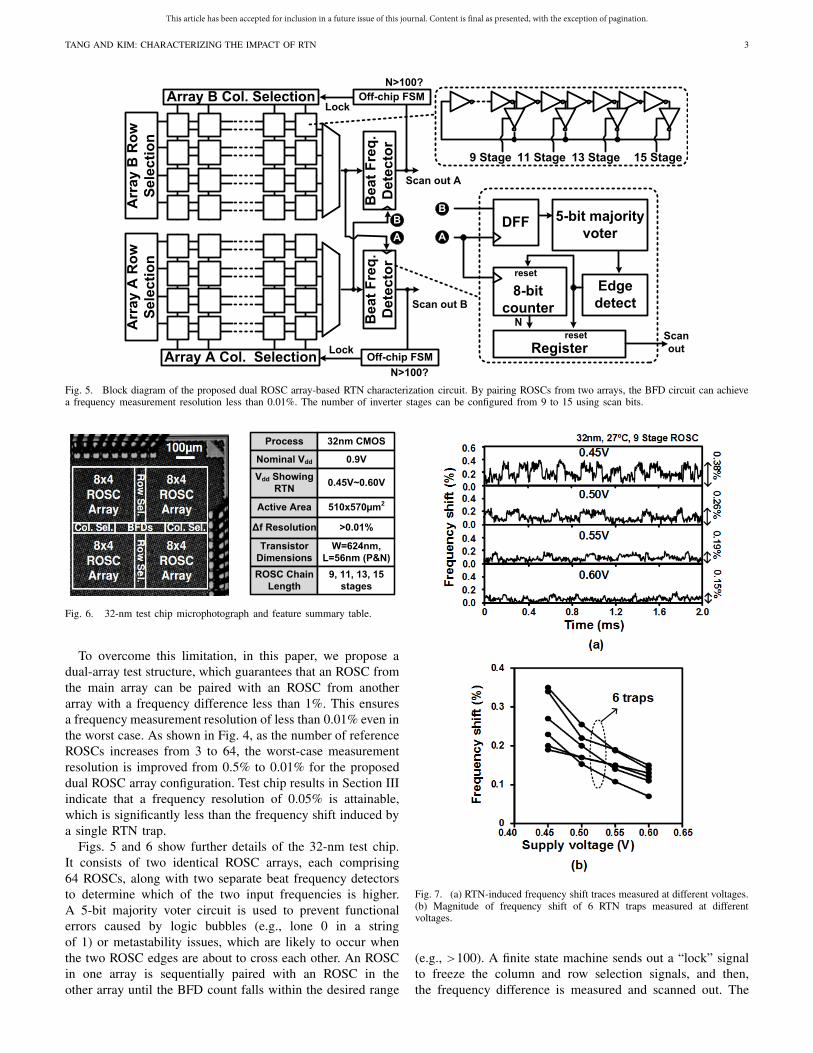
Fig. 5. Block diagram of the proposed dual ROSC array-based RTN characterization circuit. By pairing ROSCs from two arrays, the BFD circuit can achievea frequency measurement resolution less than 0.01%. The number of inverter stages can be configured from 9 to 15 using scan bits.
Fig. 6. 32-nm test chip microphotograph and feature summary table.
To overcome this limitation, in this paper, we propose adual-array test structure, which guarantees that an ROSC fromthe main array can be paired with an ROSC from anotherarray with a frequency difference less than 1%. This ensuresa frequency measurement resolution of less than 0.01% even inthe worst case. As shown in Fig. 4, as the number of referenceROSCs increases from 3 to 64, the worst-case measurementresolution is improved from 0.5% to 0.01% for the proposeddual ROSC array configuration. Test chip results in Section IIIindicate that a frequency resolution of 0.05% is attainable,which is significantly less than the frequency shift induced bya single RTN trap.
Figs. 5 and 6 show further details of the 32-nm test chip.It consists of two identical ROSC arrays, each comprising64 ROSCs, along with two separate beat frequency detectorsto determine which of the two input frequencies is higher.A 5-bit majority voter circuit is used to prevent functionalerrors caused by logic bubbles (e.g., lone 0 in a stringof 1) or metastability issues, which are likely to occur whenthe two ROSC edges are about to cross each other. An ROSCin one array is sequentially paired with an ROSC in theother array until the BFD count falls within the desired range
Fig. 7. (a) RTN-induced frequency shift traces measured at different voltages.(b) Magnitude of frequency shift of 6 RTN traps measured at differentvoltages.
(e.g., >100). A finite state machine sends out a “lock” signalto freeze the column and row selection signals, and then,the frequency difference is measured and scanned out. The
This article has been accepted for inclusion in a future issue of this journal. Content is final as presented, with the exception of pagination.
4 IEEE JOURNAL OF SOLID-STATE CIRCUITS
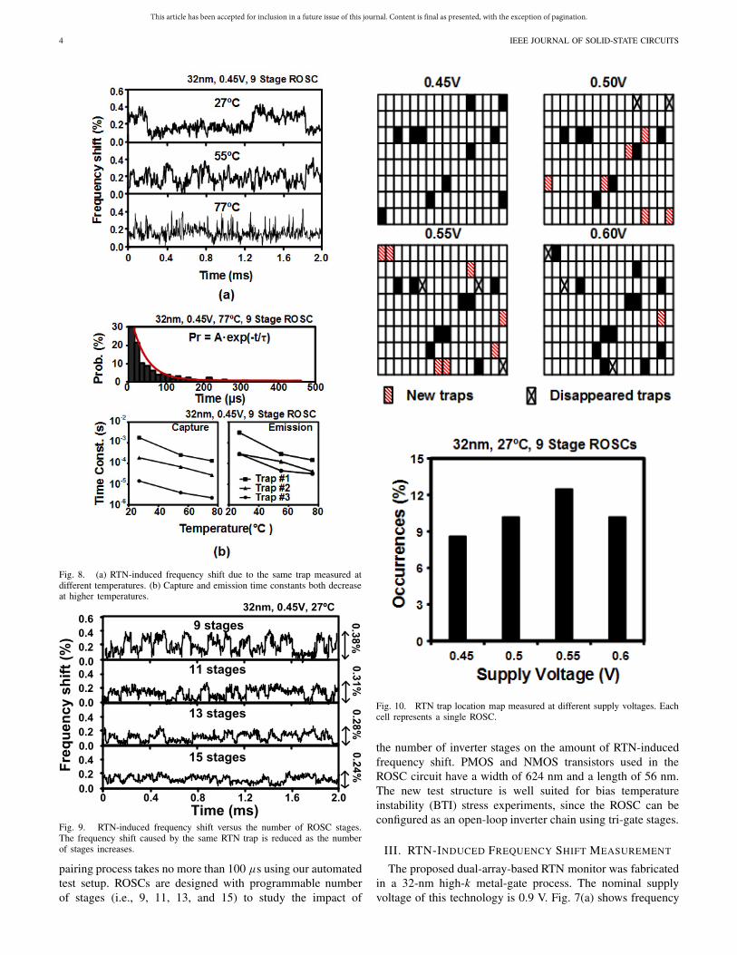
Fig. 8. (a) RTN-induced frequency shift due to the same trap measured atdifferent temperatures. (b) Capture and emission time constants both decreaseat higher temperatures.
Fig. 9. RTN-induced frequency shift versus the number of ROSC stages.The frequency shift caused by the same RTN trap is reduced as the numberof stages increases.
pairing process takes no more than 100 μs using our automatedtest setup. ROSCs are designed with programmable numberof stages (i.e., 9, 11, 13, and 15) to study the impact of
Fig. 10. RTN trap location map measured at different supply voltages. Eachcell represents a single ROSC.
the number of inverter stages on the amount of RTN-inducedfrequency shift. PMOS and NMOS transistors used in theROSC circuit have a width of 624 nm and a length of 56 nm.The new test structure is well suited for bias temperatureinstability (BTI) stress experiments, since the ROSC can beconfigured as an open-loop inverter chain using tri-gate stages.
III. RTN-INDUCED FREQUENCY SHIFT MEASUREMENT
The proposed dual-array-based RTN monitor was fabricatedin a 32-nm high-k metal-gate process. The nominal supplyvoltage of this technology is 0.9 V. Fig. 7(a) shows frequency
This article has been accepted for inclusion in a future issue of this journal. Content is final as presented, with the exception of pagination.
TANG AND KIM: CHARACTERIZING THE IMPACT OF RTN 5
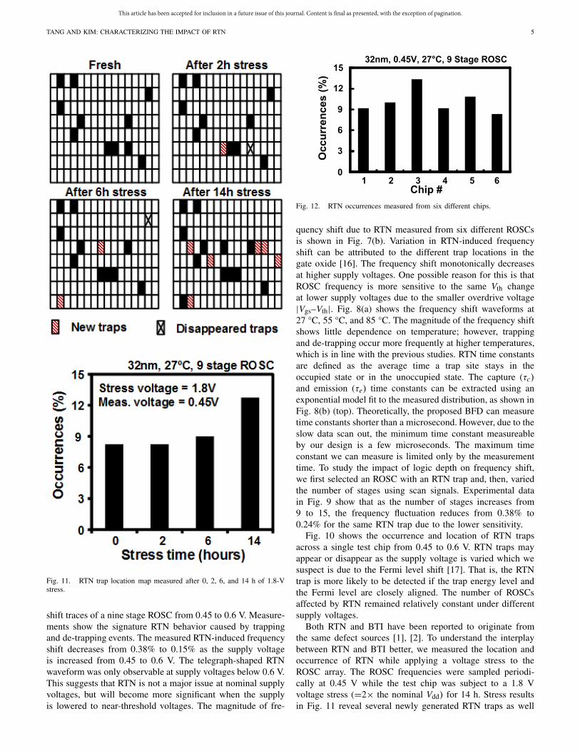
Fig. 11. RTN trap location map measured after 0, 2, 6, and 14 h of 1.8-Vstress.
shift traces of a nine stage ROSC from 0.45 to 0.6 V. Measure-ments show the signature RTN behavior caused by trappingand de-trapping events. The measured RTN-induced frequencyshift decreases from 0.38% to 0.15% as the supply voltageis increased from 0.45 to 0.6 V. The telegraph-shaped RTNwaveform was only observable at supply voltages below 0.6 V.This suggests that RTN is not a major issue at nominal supplyvoltages, but will become more significant when the supplyis lowered to near-threshold voltages. The magnitude of fre-
Fig. 12. RTN occurrences measured from six different chips.
quency shift due to RTN measured from six different ROSCsis shown in Fig. 7(b). Variation in RTN-induced frequencyshift can be attributed to the different trap locations in thegate oxide [16]. The frequency shift monotonically decreasesat higher supply voltages. One possible reason for this is thatROSC frequency is more sensitive to the same Vth changeat lower supply voltages due to the smaller overdrive voltage|Vgs–Vth|. Fig. 8(a) shows the frequency shift waveforms at27 °C, 55 °C, and 85 °C. The magnitude of the frequency shiftshows little dependence on temperature; however, trappingand de-trapping occur more frequently at higher temperatures,which is in line with the previous studies. RTN time constantsare defined as the average time a trap site stays in theoccupied state or in the unoccupied state. The capture (τc)and emission (τe) time constants can be extracted using anexponential model fit to the measured distribution, as shown inFig. 8(b) (top). Theoretically, the proposed BFD can measuretime constants shorter than a microsecond. However, due to theslow data scan out, the minimum time constant measureableby our design is a few microseconds. The maximum timeconstant we can measure is limited only by the measurementtime. To study the impact of logic depth on frequency shift,we first selected an ROSC with an RTN trap and, then, variedthe number of stages using scan signals. Experimental datain Fig. 9 show that as the number of stages increases from9 to 15, the frequency fluctuation reduces from 0.38% to0.24% for the same RTN trap due to the lower sensitivity.
Fig. 10 shows the occurrence and location of RTN trapsacross a single test chip from 0.45 to 0.6 V. RTN traps mayappear or disappear as the supply voltage is varied which wesuspect is due to the Fermi level shift [17]. That is, the RTNtrap is more likely to be detected if the trap energy level andthe Fermi level are closely aligned. The number of ROSCsaffected by RTN remained relatively constant under differentsupply voltages.
Both RTN and BTI have been reported to originate fromthe same defect sources [1], [2]. To understand the interplaybetween RTN and BTI better, we measured the location andoccurrence of RTN while applying a voltage stress to theROSC array. The ROSC frequencies were sampled periodi-cally at 0.45 V while the test chip was subject to a 1.8 Vvoltage stress (=2× the nominal Vdd) for 14 h. Stress resultsin Fig. 11 reveal several newly generated RTN traps as well
This article has been accepted for inclusion in a future issue of this journal. Content is final as presented, with the exception of pagination.
6 IEEE JOURNAL OF SOLID-STATE CIRCUITS
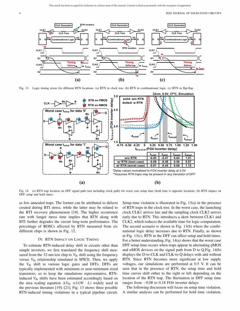
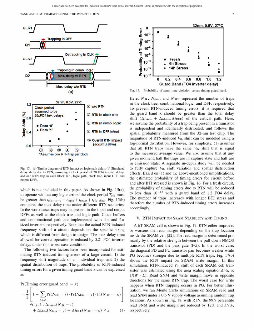
Fig. 13. Logic timing errors for different RTN locations. (a) RTN in clock tree. (b) RTN in combinational logic. (c) RTN in flip-flop.
Fig. 14. (a) RTN trap location on DFF signal path (not including clock path) for worst case setup time (hold time is opposite location). (b) RTN impact onDFF setup and hold times.
as few annealed traps. The former can be attributed to defectscreated during BTI stress, while the latter may be related tothe BTI recovery phenomenon [18]. The higher occurrencerate with longer stress time implies that RTN along withBTI further degrades the circuit long-term performance. Thepercentage of ROSCs affected by RTN measured from sixdifferent chips is shown in Fig. 12.
IV. RTN IMPACT ON LOGIC TIMING
To estimate RTN-induced delay shift in circuits other thansimple inverters, we first translated the frequency shift mea-sured from the 32-nm test chip to Vth shift using the frequencyversus Vth relationship simulated in SPICE. Then, we applythe Vth shift to various logic gates and DFFs. DFFs aretypically implemented with minimum or near-minimum sizedtransistors, so to keep the simulations representative, RTN-induced Vth shifts have been estimated accordingly based onthe area scaling equation �Vth ∝1/(W · L) widely used inthe previous literature [19]–[21]. Fig. 13 shows three possibleRTN-induced timing violations in a typical pipeline circuit.
Setup time violation is illustrated in Fig. 13(a) in the presenceof RTN traps in the clock tree. In the worst case, the launchingclock CLK1 arrives late and the sampling clock CLK2 arrivesearly due to RTN. This introduces a skew between CLK1 andCLK2, which reduces the available time for logic computation.The second scenario is shown in Fig. 13(b) where the combi-national logic delay increases due to RTN. Finally, as shownin Fig. 13(c), RTN in the DFF can affect setup and hold times.For a better understanding, Fig. 14(a) shows that the worst caseDFF setup time occurs when traps appear in alternating pMOSand nMOS devices on the signal path from D to Q.Fig. 14(b)displays the D-to-CLK and CLK-to-Q delays with and withoutRTN. Since RTN becomes more significant at low supplyvoltages, our simulations are performed at 0.5 V. It can beseen that in the presence of RTN, the setup time and holdtime curves shift either to the right or left depending on thelocation of the RTN trap. The fluctuation in DFF setup timeranges from −0.08 to 0.18 FO4 inverter delays
The following discussion will focus on setup time violation.A similar analysis can be performed for hold time violation,
This article has been accepted for inclusion in a future issue of this journal. Content is final as presented, with the exception of pagination.
TANG AND KIM: CHARACTERIZING THE IMPACT OF RTN 7
Fig. 15. (a) Timing diagram of RTN impact on logic path delay. (b) Simulateddelay shifts due to RTN, assuming a clock period of 20 FO4 inverter delaysand one RTN trap in each block (i.e., logic path, clock tree, input DFF, andoutput DFF).
which is not included in this paper. As shown in Fig. 15(a),to operate without any logic errors, the clock period Tclk mustbe greater than tclk−to−q + tlogic + tsetup + tclk_skew. Fig. 15(b)compares the max-delay time under different RTN scenarios.In the worst case, traps may be present in the input and outputDFFs as well as the clock tree and logic path. Clock buffersand combinational path are implemented with 4× and 2×sized inverters, respectively. Note that the actual RTN-inducedfrequency shift of a circuit depends on the specific sizingwhich is different from design to design. The max-delay timeallowed for correct operation is reduced by 0.21 FO4 inverterdelays under this worst-case condition.
The following two factors have been incorporated for esti-mating RTN-induced timing errors of a large circuit: 1) thefrequency shift magnitude of an individual trap; and 2) thespatial distribution of traps. The probability of RTN-inducedtiming errors for a given timing guard band x can be expressedas
Pr(Timing error|guard band = x)
= 1
2
⎡⎣1 −
∑i, j,k
Pr(Nclk = i) · Pr(Ndata = j) · Pr(NDFF = k)
⎤⎦
∀i, j, k : �tskew(Nclk = i)
+ �tdata(Ndata = j) + �tDFF(NDFF = k) ≤ x (1)
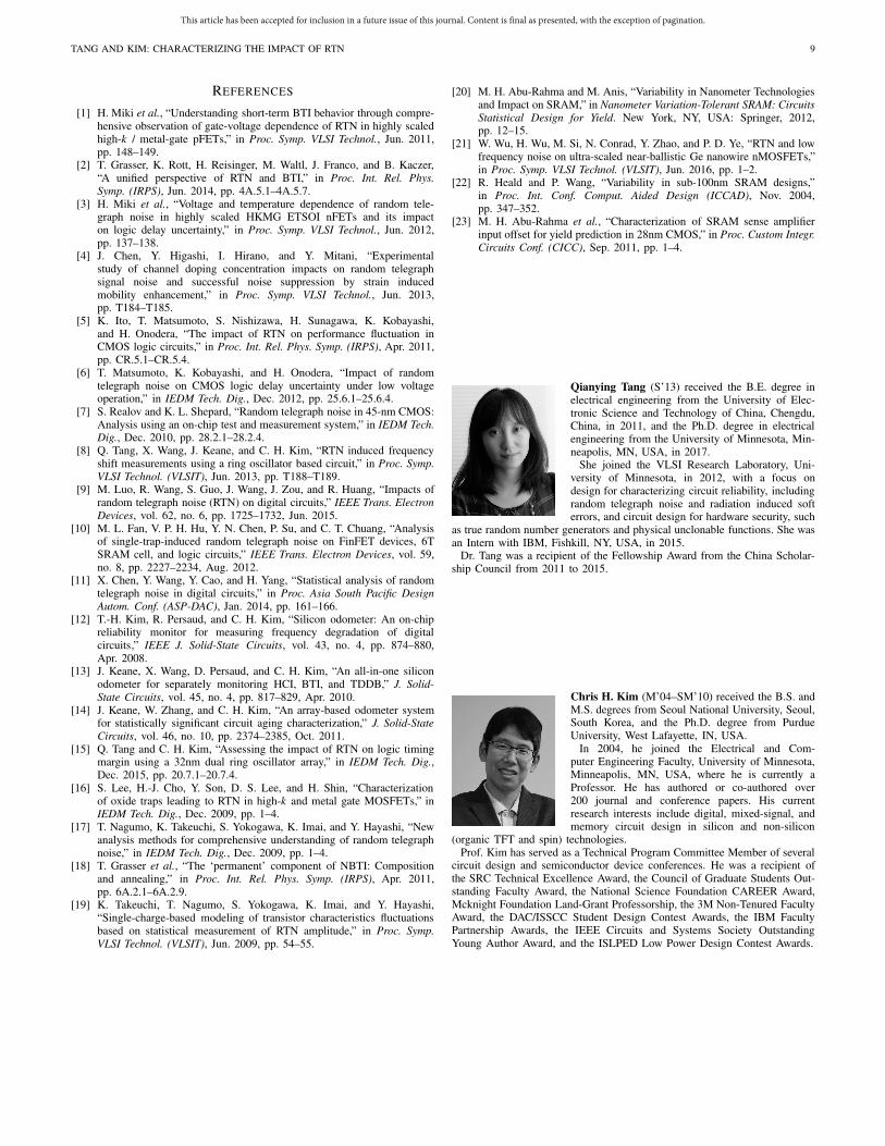
Fig. 16. Probability of setup time violation versus timing guard band.
Here, Nclk , Ndata, and NDFF represent the number of trapsin the clock tree, combinational logic, and DFF, respectively.To prevent RTN-induced timing errors, it is required thatthe guard band x should be greater than the total delayshift (�tskew + �tdata+�tDFF) of the critical path. Here,we assume the probability of a trap being present in a transistoris independent and identically distributed, and follows thespatial probability measured from the 32-nm test chip. Themagnitude of RTN-induced Vth shift can be modeled using alog-normal distribution. However, for simplicity, (1) assumesthat all RTN traps have the same Vth shift that is equalto the measured average value. We also assume that at anygiven moment, half the traps are in capture state and half arein emission state. A separate in-depth study will be neededto fully capture Vth shift variation and spatial distributioneffects. Based on (1) and the above-mentioned simplifications,the estimated probability of timing errors for circuit beforeand after BTI stressed is shown in Fig. 16. For a fresh circuit,the probability of timing errors due to RTN will be reducedto less than 10−12 with a guard band of 1.2 FO4 delay.The number of traps increases with longer BTI stress andtherefore the number of RTN-induced timing errors increasesaccordingly.
V. RTN IMPACT ON SRAM STABILITY AND TIMING
A 6T SRAM cell is shown in Fig. 17. RTN either improvesor worsens the read margin depending on the trap locationinside the SRAM cell [22]. The read margin is determined pri-marily by the relative strength between the pull down NMOStransistor (PD) and the pass gate (PG). In the worst case,the diagonal PD and PU transistor pair becomes weaker whilePG becomes stronger due to multiple RTN traps. Fig. 17(b)shows the RTN impact on SRAM write margin. In thissimulation, RTN-induced Vth shift of each SRAM cell tran-sistor was estimated using the area scaling equation�Vth ∝1/(W · L). Read SNM and write margin move in oppositedirections for the same RTN trap. The worst case for writehappens when RTN trapping occurs in PG. For better illus-tration, we ran Monte Carlo simulations on SRAM read andread SNM under a 0.6 V supply voltage assuming random traplocations. As shown in Fig. 18, with RTN, the 99.9 percentileread SNM and write margin are reduced by 12% and 3.9%,respectively.

This article has been accepted for inclusion in a future issue of this journal. Content is final as presented, with the exception of pagination.
8 IEEE JOURNAL OF SOLID-STATE CIRCUITS
Fig. 17. RTN impact on SRAM (a) read SNM and (b) write margin.
Fig. 18. Monte Carlo simulations of SRAM (a) read SNM and (b) writemargin, with and without RTN.
Next, we analyze how the SRAM read path delay, namelythe CLK to DOUT delay, is affected by RTN. Fig. 19 showsthe schematic and timing diagram of a 128-kbit SRAMsubarray used in this discussion. First, when RTN traps arepresent in the row decoder, the CLK to WL delay increasescausing the read delay to increase. Similarly, read delay mayincrease due to RTN traps in the sense amplifier enablesignal (SAE) generation path. The worst case read delayoccurs when the trap is located in the PG transistors becauseSRAM read speed is determined by the read current. Finally,RTN in the sense amplifier may degrade the resolving time.Fig. 20 shows a typical latch based sense amplifier. WhenBitLine is discharged, traps on transistors 2 and 3 increasethe SAE to DOUT delay while traps on transistors 4 and5 decrease the delay. RTN has a stronger impact on senseamplifier delay for smaller bitline voltage differences.
To capture the above discussion, we simulated the CLK toDOUT delay of a realistic 128-kbit SRAM sub-array in 32-nmtechnology assuming traps in different locations. Considering
Fig. 19. RTN impact on SRAM read timing.
Fig. 20. RTN impact on sense amplifier resolving time.
Fig. 21. RTN impact on SRAM read path delay.
that transistors on the critical path have different sizing andfan-out, the RTN-induced Vth shift was applied to the mostsensitive stage while the Vth shift was estimated using thearea scaling equation. For the sense amplifier, we assumedthe input transistors have a W/L of 624 nm/56 nm which iscomparable to the sizing used in an industrial design [23].As shown in Fig. 21, traps located in the row decoder shownegligible impact on the overall read delay while traps in thesense amplifier have a greater impact. Assuming a scenarioin which a single RTN trap exists in each block (i.e., rowdecoder, SRAM access transistor, sense amplifier, and SRlatch), the read path delay increases by 0.51% at 0.6 V andby 0.90% at 0.55 V.
VI. CONCLUSION
In this paper, we present an array-based circuit for detailedcharacterization of RTN-induced frequency shift, fabricatedin a 32-nm technology. A novel dual ROSC array structurebased on the tested-and-proven BFD technique enables fullyautomated collection of RTN statistics with high measurementaccuracy at supply voltages as low as 0.45 V. The magnitudeand occurrences of RTN-induced ROSC frequency shift weremeasured under different supply voltages, temperatures, andvoltage stress conditions. Based on the measured frequencyshift data, we estimated the RTN impact on logic timingmargins and SRAM performance.
This article has been accepted for inclusion in a future issue of this journal. Content is final as presented, with the exception of pagination.
TANG AND KIM: CHARACTERIZING THE IMPACT OF RTN 9
REFERENCES
[1] H. Miki et al., “Understanding short-term BTI behavior through compre-hensive observation of gate-voltage dependence of RTN in highly scaledhigh-k / metal-gate pFETs,” in Proc. Symp. VLSI Technol., Jun. 2011,pp. 148–149.
[2] T. Grasser, K. Rott, H. Reisinger, M. Waltl, J. Franco, and B. Kaczer,“A unified perspective of RTN and BTI,” in Proc. Int. Rel. Phys.Symp. (IRPS), Jun. 2014, pp. 4A.5.1–4A.5.7.
[3] H. Miki et al., “Voltage and temperature dependence of random tele-graph noise in highly scaled HKMG ETSOI nFETs and its impacton logic delay uncertainty,” in Proc. Symp. VLSI Technol., Jun. 2012,pp. 137–138.
[4] J. Chen, Y. Higashi, I. Hirano, and Y. Mitani, “Experimentalstudy of channel doping concentration impacts on random telegraphsignal noise and successful noise suppression by strain inducedmobility enhancement,” in Proc. Symp. VLSI Technol., Jun. 2013,pp. T184–T185.
[5] K. Ito, T. Matsumoto, S. Nishizawa, H. Sunagawa, K. Kobayashi,and H. Onodera, “The impact of RTN on performance fluctuation inCMOS logic circuits,” in Proc. Int. Rel. Phys. Symp. (IRPS), Apr. 2011,pp. CR.5.1–CR.5.4.
[6] T. Matsumoto, K. Kobayashi, and H. Onodera, “Impact of randomtelegraph noise on CMOS logic delay uncertainty under low voltageoperation,” in IEDM Tech. Dig., Dec. 2012, pp. 25.6.1–25.6.4.
[7] S. Realov and K. L. Shepard, “Random telegraph noise in 45-nm CMOS:Analysis using an on-chip test and measurement system,” in IEDM Tech.Dig., Dec. 2010, pp. 28.2.1–28.2.4.
[8] Q. Tang, X. Wang, J. Keane, and C. H. Kim, “RTN induced frequencyshift measurements using a ring oscillator based circuit,” in Proc. Symp.VLSI Technol. (VLSIT), Jun. 2013, pp. T188–T189.
[9] M. Luo, R. Wang, S. Guo, J. Wang, J. Zou, and R. Huang, “Impacts ofrandom telegraph noise (RTN) on digital circuits,” IEEE Trans. ElectronDevices, vol. 62, no. 6, pp. 1725–1732, Jun. 2015.
[10] M. L. Fan, V. P. H. Hu, Y. N. Chen, P. Su, and C. T. Chuang, “Analysisof single-trap-induced random telegraph noise on FinFET devices, 6TSRAM cell, and logic circuits,” IEEE Trans. Electron Devices, vol. 59,no. 8, pp. 2227–2234, Aug. 2012.
[11] X. Chen, Y. Wang, Y. Cao, and H. Yang, “Statistical analysis of randomtelegraph noise in digital circuits,” in Proc. Asia South Pacific DesignAutom. Conf. (ASP-DAC), Jan. 2014, pp. 161–166.
[12] T.-H. Kim, R. Persaud, and C. H. Kim, “Silicon odometer: An on-chipreliability monitor for measuring frequency degradation of digitalcircuits,” IEEE J. Solid-State Circuits, vol. 43, no. 4, pp. 874–880,Apr. 2008.
[13] J. Keane, X. Wang, D. Persaud, and C. H. Kim, “An all-in-one siliconodometer for separately monitoring HCI, BTI, and TDDB,” J. Solid-State Circuits, vol. 45, no. 4, pp. 817–829, Apr. 2010.
[14] J. Keane, W. Zhang, and C. H. Kim, “An array-based odometer systemfor statistically significant circuit aging characterization,” J. Solid-StateCircuits, vol. 46, no. 10, pp. 2374–2385, Oct. 2011.
[15] Q. Tang and C. H. Kim, “Assessing the impact of RTN on logic timingmargin using a 32nm dual ring oscillator array,” in IEDM Tech. Dig.,Dec. 2015, pp. 20.7.1–20.7.4.
[16] S. Lee, H.-J. Cho, Y. Son, D. S. Lee, and H. Shin, “Characterizationof oxide traps leading to RTN in high-k and metal gate MOSFETs,” inIEDM Tech. Dig., Dec. 2009, pp. 1–4.
[17] T. Nagumo, K. Takeuchi, S. Yokogawa, K. Imai, and Y. Hayashi, “Newanalysis methods for comprehensive understanding of random telegraphnoise,” in IEDM Tech. Dig., Dec. 2009, pp. 1–4.
[18] T. Grasser et al., “The ‘permanent’ component of NBTI: Compositionand annealing,” in Proc. Int. Rel. Phys. Symp. (IRPS), Apr. 2011,pp. 6A.2.1–6A.2.9.
[19] K. Takeuchi, T. Nagumo, S. Yokogawa, K. Imai, and Y. Hayashi,“Single-charge-based modeling of transistor characteristics fluctuationsbased on statistical measurement of RTN amplitude,” in Proc. Symp.VLSI Technol. (VLSIT), Jun. 2009, pp. 54–55.
[20] M. H. Abu-Rahma and M. Anis, “Variability in Nanometer Technologiesand Impact on SRAM,” in Nanometer Variation-Tolerant SRAM: CircuitsStatistical Design for Yield. New York, NY, USA: Springer, 2012,pp. 12–15.
[21] W. Wu, H. Wu, M. Si, N. Conrad, Y. Zhao, and P. D. Ye, “RTN and lowfrequency noise on ultra-scaled near-ballistic Ge nanowire nMOSFETs,”in Proc. Symp. VLSI Technol. (VLSIT), Jun. 2016, pp. 1–2.
[22] R. Heald and P. Wang, “Variability in sub-100nm SRAM designs,”in Proc. Int. Conf. Comput. Aided Design (ICCAD), Nov. 2004,pp. 347–352.
[23] M. H. Abu-Rahma et al., “Characterization of SRAM sense amplifierinput offset for yield prediction in 28nm CMOS,” in Proc. Custom Integr.Circuits Conf. (CICC), Sep. 2011, pp. 1–4.
Qianying Tang (S’13) received the B.E. degree inelectrical engineering from the University of Elec-tronic Science and Technology of China, Chengdu,China, in 2011, and the Ph.D. degree in electricalengineering from the University of Minnesota, Min-neapolis, MN, USA, in 2017.
She joined the VLSI Research Laboratory, Uni-versity of Minnesota, in 2012, with a focus ondesign for characterizing circuit reliability, includingrandom telegraph noise and radiation induced softerrors, and circuit design for hardware security, such
as true random number generators and physical unclonable functions. She wasan Intern with IBM, Fishkill, NY, USA, in 2015.
Dr. Tang was a recipient of the Fellowship Award from the China Scholar-ship Council from 2011 to 2015.
Chris H. Kim (M’04–SM’10) received the B.S. andM.S. degrees from Seoul National University, Seoul,South Korea, and the Ph.D. degree from PurdueUniversity, West Lafayette, IN, USA.
In 2004, he joined the Electrical and Com-puter Engineering Faculty, University of Minnesota,Minneapolis, MN, USA, where he is currently aProfessor. He has authored or co-authored over200 journal and conference papers. His currentresearch interests include digital, mixed-signal, andmemory circuit design in silicon and non-silicon
(organic TFT and spin) technologies.Prof. Kim has served as a Technical Program Committee Member of several
circuit design and semiconductor device conferences. He was a recipient ofthe SRC Technical Excellence Award, the Council of Graduate Students Out-standing Faculty Award, the National Science Foundation CAREER Award,Mcknight Foundation Land-Grant Professorship, the 3M Non-Tenured FacultyAward, the DAC/ISSCC Student Design Contest Awards, the IBM FacultyPartnership Awards, the IEEE Circuits and Systems Society OutstandingYoung Author Award, and the ISLPED Low Power Design Contest Awards.