high frequency low-jitter phase-locked loop design - emo
TRANSCRIPT

HIGH FREQUENCY LOW-JITTERPHASE-LOCKED LOOP DESIGN
by
Onur KAZANC
Engineering Project Report
Yeditepe University
Faculty of Engineering and Architecture
Department of Electrical and Electronics Engineering
Istanbul, 2008

ii
HIGH FREQUENCY LOW-JITTERPHASE-LOCKED LOOP DESIGN
APPROVED BY:
Dr. Bortecene Terlemez . . . . . . . . . . . . . . . . . . . . . . . . . .
(Supervisor)
Prof. Dr. Ugur Cilingiroglu . . . . . . . . . . . . . . . . . . . . . . . .. .
Asst. Prof. Dr. Korkut Yegin . . . . . . . . . . . . . . . . . . . . . . . . . .
DATE OF APPROVAL: ....................................

iii
ABSTRACT
Advances in CMOS technology permits realization of high speed and low noise integrated
frequency synthesizers and reduction in system costs. Thisproject covers analysis, design and
simulation of a high frequency low phase noise CMOS Phase Locked Loop (PLL) frequency
synthesizer with TSMC 0.18µm process of Taiwan Semiconductor Manufacturing Company.
Starting with the PLL basics, behavioral analysis and CMOS implementation of various PLL
blocks are introduced at first place. This research mainly investigates how to reduce second
order effects of each PLL block which could possibly cause increase PLL phase noise (and/or
spurs) with an emphasis on how to reduce VCO noise contribution. In Conclusion section a
summary of factors involving the design is given.

iv
OZET
CMOS teknolojisindeki ilerlemeler yuksek hızda dusukgurultulu frekans sentezleyici-
lerin dusuk maliyetle uretimini mumkun kılmaktadır. Bu proje TSMC 0.18µm prosesi ile yuksek
hızlı dusuk faz gurultulu PLL frekans sentezleyicinin analiz, tasarım ve simulasyonunu kap-
samaktadır. PLL temellerinden baslayarak, oncelikle PLL yapıtaslarının davranıssal analizi ve
CMOS transistor seviyesinde gerceklenmesi ele alınmıstır. Bu arastırmada temel olarak PLL
yapıtaslarında yuksek faz gurultusune neden olan ikincil etkileri azaltmaya yonelik yontemlerle
birlikte ozellikle gerilim kontrollu osilatorun (VCO) faz gurultusunun azaltılması uzerinde du-
ruldu. Sonuc bolumunde ise PLL tasarımını ilgilendiren faktorler ozet olarak verilmistir.

v
TABLE OF CONTENTS
ABSTRACT . . . . . . . . . . . . . . . . . . . . . . . . . . . . . . . . . . . . . . . . iii
OZET . . . . . . . . . . . . . . . . . . . . . . . . . . . . . . . . . . . . . . . . . . . iv
LIST OF FIGURES . . . . . . . . . . . . . . . . . . . . . . . . . . . . . . . . . . . . vii
LIST OF TABLES . . . . . . . . . . . . . . . . . . . . . . . . . . . . . . . . . . . . . xiii
1. INTRODUCTION . . . . . . . . . . . . . . . . . . . . . . . . . . . . . . . . . . . 1
1.1. PLL Applications . . . . . . . . . . . . . . . . . . . . . . . . . . . . . . . .. 1
1.2. PLL Basics . . . . . . . . . . . . . . . . . . . . . . . . . . . . . . . . . . . . 3
2. PHASE FREQUENCY DETECTOR. . . . . . . . . . . . . . . . . . . . . . . . . 5
2.1. Phase Frequency Detector Operation . . . . . . . . . . . . . . . .. . . . . . . 5
2.2. PFD Design and Simulation . . . . . . . . . . . . . . . . . . . . . . . . .. . 7
3. CHARGE PUMP . . . . . . . . . . . . . . . . . . . . . . . . . . . . . . . . . . . 12
3.1. Charge Pump Operation . . . . . . . . . . . . . . . . . . . . . . . . . . . .. . 12
3.2. Charge Pump Design and Simulation . . . . . . . . . . . . . . . . . .. . . . . 15
4. VOLTAGE CONTROLLED OSCILLATORS . . . . . . . . . . . . . . . . . . . . . 23
4.1. Integrated Oscillators . . . . . . . . . . . . . . . . . . . . . . . . . .. . . . . 23
4.1.1. Oscillation Principles . . . . . . . . . . . . . . . . . . . . . . . .. . . 23
4.1.2. Types of Integrated Oscillators . . . . . . . . . . . . . . . . .. . . . . 24
4.2. CMOS Ring Oscillators . . . . . . . . . . . . . . . . . . . . . . . . . . . .. . 25
4.2.1. Ring Oscillator Basics . . . . . . . . . . . . . . . . . . . . . . . . .. 25
4.2.2. Single Ended Ring Oscillator . . . . . . . . . . . . . . . . . . . .. . . 27
4.2.3. Differential Ring Oscillator . . . . . . . . . . . . . . . . . . .. . . . . 28
4.3. Noise Sources . . . . . . . . . . . . . . . . . . . . . . . . . . . . . . . . . . .30
4.3.1. Thermal Noise . . . . . . . . . . . . . . . . . . . . . . . . . . . . . . 31
4.3.2. Flicker Noise . . . . . . . . . . . . . . . . . . . . . . . . . . . . . . . 31
4.4. Phase Noise . . . . . . . . . . . . . . . . . . . . . . . . . . . . . . . . . . . . 32
4.5. Ring VCO Design and Simulation . . . . . . . . . . . . . . . . . . . . .. . . 35

vi
5. FEEDBACK DIVIDER . . . . . . . . . . . . . . . . . . . . . . . . . . . . . . . . 47
6. LOOP DYNAMICS . . . . . . . . . . . . . . . . . . . . . . . . . . . . . . . . . . 55
6.1. Transfer Functions . . . . . . . . . . . . . . . . . . . . . . . . . . . . . .. . 55
6.2. Loop Filter Design . . . . . . . . . . . . . . . . . . . . . . . . . . . . . . .. 57
6.2.1. Loop Filter Implementation with MOSFET Capacitance. . . . . . . . 63
7. TOP LEVEL PLL SIMULATION . . . . . . . . . . . . . . . . . . . . . . . . . . . 67
7.1. Transient Simulation . . . . . . . . . . . . . . . . . . . . . . . . . . . .. . . 67
7.2. Phase Noise Analysis of PLL . . . . . . . . . . . . . . . . . . . . . . . .. . . 69
8. CONCLUSION . . . . . . . . . . . . . . . . . . . . . . . . . . . . . . . . . . . . 72
APPENDIX A: Logical Effort . . . . . . . . . . . . . . . . . . . . . . . . . . . . . . 74
A.1. Delay in a Logic Gate . . . . . . . . . . . . . . . . . . . . . . . . . . . . . .. 74
A.2. Multistage Logic Networks . . . . . . . . . . . . . . . . . . . . . . . .. . . . 76
APPENDIX B: MATLAB Loop Filter Design Script . . . . . . . . . . . . . . . . . . 81
REFERENCES . . . . . . . . . . . . . . . . . . . . . . . . . . . . . . . . . . . . . . 84

vii
LIST OF FIGURES
Figure 1.1. Timing jitter . . . . . . . . . . . . . . . . . . . . . . . . . . . . .. . . . 1
Figure 1.2. Clock skew in a digital system . . . . . . . . . . . . . . . .. . . . . . . 2
Figure 1.3. Timing jitter . . . . . . . . . . . . . . . . . . . . . . . . . . . . .. . . . 3
Figure 1.4. Block diagram of a basic PLL . . . . . . . . . . . . . . . . . .. . . . . 4
Figure 2.1. PFD Block Diagram . . . . . . . . . . . . . . . . . . . . . . . . . .. . . 5
Figure 2.2. PFD State Diagram . . . . . . . . . . . . . . . . . . . . . . . . . .. . . 6
Figure 2.3. Operation of PFD . . . . . . . . . . . . . . . . . . . . . . . . . . .. . . 6
Figure 2.4. PFD characteristic . . . . . . . . . . . . . . . . . . . . . . . .. . . . . . 7
Figure 2.5. PFD models . . . . . . . . . . . . . . . . . . . . . . . . . . . . . . . .. 8
Figure 2.6. Output configuration to generate complementarysignals . . . . . . . . . 8
Figure 2.7. Effect of transmission gate on output matching .. . . . . . . . . . . . . . 9
Figure 2.8. PFD power dissipation versus frequency . . . . . . .. . . . . . . . . . . 10
Figure 2.9. PFD simulation for three modes of operation . . . .. . . . . . . . . . . . 11

viii
Figure 3.1. Charge Pump schematic . . . . . . . . . . . . . . . . . . . . . .. . . . . 12
Figure 3.2. PFD-CP Operation . . . . . . . . . . . . . . . . . . . . . . . . . .. . . 13
Figure 3.3. Charge Pump charging and discharging output capacitor . . . . . . . . . . 14
Figure 3.4. Charge Pump dead zone . . . . . . . . . . . . . . . . . . . . . . .. . . . 14
Figure 3.5. High swing low voltage cascode reference . . . . . .. . . . . . . . . . . 15
Figure 3.6. Bandgap based current reference for charge pump. . . . . . . . . . . . . 16
Figure 3.7. Transient response of reference circuit . . . . . .. . . . . . . . . . . . . 17
Figure 3.8. Charge sharing in charge pump . . . . . . . . . . . . . . . .. . . . . . . 18
Figure 3.9. Charge Pump with a unity gain amplifier . . . . . . . . .. . . . . . . . . 18
Figure 3.10. Charge pump linear operation region . . . . . . . . .. . . . . . . . . . . 19
Figure 3.11. Effect of channel charge injection . . . . . . . . . .. . . . . . . . . . . 20
Figure 3.12. Clock feedthrough in a MOSFET . . . . . . . . . . . . . . .. . . . . . . 21
Figure 3.13. Charge pump with dummy switches . . . . . . . . . . . . .. . . . . . . 22
Figure 4.1. Feedback System . . . . . . . . . . . . . . . . . . . . . . . . . . .. . . 23
Figure 4.2. Representation of positive feedback . . . . . . . . .. . . . . . . . . . . 24

ix
Figure 4.3. Single stage inverter and amplifier . . . . . . . . . . .. . . . . . . . . . 25
Figure 4.4. Two stage inverter . . . . . . . . . . . . . . . . . . . . . . . . .. . . . . 26
Figure 4.5. Three stage inverter . . . . . . . . . . . . . . . . . . . . . . .. . . . . . 26
Figure 4.6. Three stage ring oscillator . . . . . . . . . . . . . . . . .. . . . . . . . . 27
Figure 4.7. Current-starved inverter . . . . . . . . . . . . . . . . . .. . . . . . . . . 28
Figure 4.8. Capacitive tuning . . . . . . . . . . . . . . . . . . . . . . . . .. . . . . 28
Figure 4.9. Differential Ring Oscillator . . . . . . . . . . . . . . .. . . . . . . . . . 29
Figure 4.10. Differential delay stage with different load types . . . . . . . . . . . . . . 30
Figure 4.11. Spectrum of Thermal Noise . . . . . . . . . . . . . . . . . .. . . . . . . 31
Figure 4.12. Spectrum of Flicker Noise . . . . . . . . . . . . . . . . . .. . . . . . . 31
Figure 4.13. Effect of phase noise on an oscillator . . . . . . . .. . . . . . . . . . . . 32
Figure 4.14. Phase noise calculation around the carrier . . .. . . . . . . . . . . . . . 33
Figure 4.15. Effect of phase noise on a reciever . . . . . . . . . . .. . . . . . . . . . 34
Figure 4.16. Effect of jitter on clock edges . . . . . . . . . . . . . .. . . . . . . . . . 35
Figure 4.17. VCO block diagram . . . . . . . . . . . . . . . . . . . . . . . . .. . . . 36

x
Figure 4.18. N-Stage ring oscillator with bias stage . . . . . .. . . . . . . . . . . . . 36
Figure 4.19. VCO V2I circuit . . . . . . . . . . . . . . . . . . . . . . . . . . .. . . . 37
Figure 4.20. Delay cell with symmetric loads . . . . . . . . . . . . .. . . . . . . . . 39
Figure 4.21. Symmetric V-I characteristic of delay cell load . . . . . . . . . . . . . . . 40
Figure 4.22. VCO output buffer block diagram . . . . . . . . . . . . .. . . . . . . . 41
Figure 4.23. Low-swing buffer . . . . . . . . . . . . . . . . . . . . . . . . .. . . . . 41
Figure 4.24. Differential to single-ended converter . . . . .. . . . . . . . . . . . . . . 42
Figure 4.25. 8-Stage inverter chain . . . . . . . . . . . . . . . . . . . .. . . . . . . . 43
Figure 4.26. VCO frequency versus control voltage . . . . . . . .. . . . . . . . . . . 43
Figure 4.27. DC characteristic of delay cell . . . . . . . . . . . . .. . . . . . . . . . 44
Figure 4.28. Consecutive outputs of VCO . . . . . . . . . . . . . . . . .. . . . . . . 45
Figure 4.29. Phase Noise of VCO . . . . . . . . . . . . . . . . . . . . . . . . .. . . 46
Figure 5.1. Frequency multiplication in PLL . . . . . . . . . . . . .. . . . . . . . . 47
Figure 5.2. Programmable divider with 2/3 cells . . . . . . . . . .. . . . . . . . . . 48
Figure 5.3. 2/3 divider cell schematic . . . . . . . . . . . . . . . . . .. . . . . . . . 49
xi
Figure 5.4. CML blocks . . . . . . . . . . . . . . . . . . . . . . . . . . . . . . . .. 50
Figure 5.5. CML Latch design model . . . . . . . . . . . . . . . . . . . . . .. . . . 51
Figure 5.6. Output of 2/3 divider cell . . . . . . . . . . . . . . . . . . .. . . . . . . 52
Figure 5.7. Divide-by-20 built with 2/3 cells . . . . . . . . . . . .. . . . . . . . . . 52
Figure 5.8. Divide-by-20 operation for input clock at 2.5 GHz . . . . . . . . . . . . . 53
Figure 6.1. PLL blocks with transfer functions . . . . . . . . . . .. . . . . . . . . . 55
Figure 6.2. PLL transfer functions with divider and charge pump added . . . . . . . . 58
Figure 6.3. Second order PLL loop filter . . . . . . . . . . . . . . . . . .. . . . . . 58
Figure 6.4. Bode-plot of PLL open loop transfer function . . .. . . . . . . . . . . . 59
Figure 6.5. Output of two functions for 3dB frequency ratio .. . . . . . . . . . . . . 61
Figure 6.6. Natural frequency versus loop filter capacitance (C1) . . . . . . . . . . . 62
Figure 6.7. Open-Loop AC response of PLL . . . . . . . . . . . . . . . . .. . . . . 63
Figure 6.8. Closed-loop AC response of PLL . . . . . . . . . . . . . . .. . . . . . . 64
Figure 6.9. Loop filter implementation with NMOS capacitance . . . . . . . . . . . . 64
Figure 6.10. Charging of ideal capacitor and MOS capacitor .. . . . . . . . . . . . . 65

xii
Figure 6.11. Resistance variation versus temperature and process . . . . . . . . . . . . 66
Figure 7.1. PLL top-level Simulation - Kickstart . . . . . . . . .. . . . . . . . . . . 67
Figure 7.2. PLL top-level simulation - Step after lock . . . . .. . . . . . . . . . . . 68
Figure 7.3. Phase domain model of PLL . . . . . . . . . . . . . . . . . . . .. . . . 69
Figure 7.4. PLL Phase Noise . . . . . . . . . . . . . . . . . . . . . . . . . . . .. . 70
Figure A.1. Delay Values of different logic gates . . . . . . . . .. . . . . . . . . . . 75
Figure A.2. Plots of delay equation for an inverter and two-input NAND gate . . . . . 76
Figure A.3. An inverter driving four identical inverters . .. . . . . . . . . . . . . . . 77
Figure A.4. Multistage path with different gates . . . . . . . . .. . . . . . . . . . . . 79

xiii
LIST OF TABLES
Table 2.1. Minimum pulse widths of PFD . . . . . . . . . . . . . . . . . . .. . . . 8
Table 2.2. PFD Perfomance Summary . . . . . . . . . . . . . . . . . . . . . .. . . 10
Table 3.1. Charge pump currents and mismatch in corners . . . .. . . . . . . . . . . 20
Table 3.2. Charge Pump Summary . . . . . . . . . . . . . . . . . . . . . . . . .. . 22
Table 4.1. Device dimensions of V2I circuit . . . . . . . . . . . . . .. . . . . . . . 38
Table 4.2. Device dimensions of delay cell with symmetric loads . . . . . . . . . . . 40
Table 6.1. Loop Filter NMOS Capacitance Parameters . . . . . . .. . . . . . . . . 65
Table 8.1. PLL Summary . . . . . . . . . . . . . . . . . . . . . . . . . . . . . . . .73

1
1. INTRODUCTION
Phase-Locked Loops (PLLs) find wide application in areas such as communications, wire-
less systems, digital circuits, and disk drive electronics. While the concept of phase locking
has been in use for more than half a century, monolithic implementation of PLLs has become
possible only in the last thirty years and become popular. Two factors account for this trend:
the demand for higher performance and lower cost in electronic systems, and the advance of
integrated-circuit (IC) technologies in terms of speed andcomplexity.
1.1. PLL Applications
Phase locking is a powerful technique that can provide elegant solutions in many applica-
tions. The design problems that can be efficiently solved with the aid of PLLs [1] are summa-
rized as follows.
• Jitter Reduction
Signals often experience timing jitter as they travel through a communication channel or as they
are retrieved from a storage medium. Shown in Figure 4.16, jitter causes variation in the period
of a waveform, a type of error that cannot be removed by amplification and clipping even if the
signal is binary. A PLL can be used to reduce the jitter.
Figure 1.1. Timing jitter

2
• Skew Cancellation
Figure 1.2 illustrates a critical problem in high-speed digital systems. Here, a system clock,
CKS, enters a chip from a printed-circuit board (PCB) and is buffered (in several stages) to
sharpen its edges and drive the load capacitance with minimal delay. The principal difficulty
in such an arrangement is that the on-chip clock,CKC , typically drives several nanofarads of
device and interconnect capacitance, exhibiting significant delay with respect toCKS. The
resulting skew reduces the timing budget for on-chip and inter-chip operations. In order to
lower the skew, the clock buffer can be placed in a phase-locked loop, thereby aligningCKC
with CKS.
Figure 1.2. Clock skew in a digital system
• Frequency Synthesis
Many applications require frequency multiplication of periodic signals. For example, in the
digital system of Figure 1.2, the bandwidth limitation of PCboards constrains the frequency of
CKS, whereas the on-chip clock frequency may need to be much higher. As another example,
wireless transceivers employ a local oscillator whose output frequency must be varied in small,
precise steps, for example, from 900 MHz to 925 MHz in steps of200 kHz. These exemplify
the problem of “frequency synthesis”, a task performed efficiently using phase-locked systems.

3
• Clock Recovery
In many systems, data is transmitted or retrieved without any additional timing reference. In
optical communications, for example, a stream of data flows over a single fiber with no ac-
companying clock, but the receiver must eventually processthe data synchronously. Thus, the
timing information (e.g. the clock) must be recovered from the data at the receive end (Figure
1.3). Most clock recovery circuits employ phase locking.
Figure 1.3. Timing jitter
1.2. PLL Basics
A phase-locked loop is a feedback system that operates on theexcess phase of nominally
periodic signals. This is in contrast to familiar feedback circuits where voltage and current
amplitudes and their rate of change are of interest. Shown inFigure 1.4, a phase-locked loop
contains three basic components:
• A phase-detector (PD).
• A loop-filter (LPF).
• A voltage-controlled oscillator (VCO).
The phase-detector compares the phase of the input signal, x(t), against the phase of the
VCO output signal, y(t). Output of the phase-detector is a voltage proportional to the phase
difference between its two inputs. The loop is considered “locked” if the phase difference is
constant with time. The difference voltage at the phase-detector output is filtered by the loop-

4
Figure 1.4. Block diagram of a basic PLL
filter. Loop-filter is a lowpass filter, which suppresses the high frequency signal components and
noise. Output of the loop-filter is applied to the VCO as the control voltage. This control voltage
changes the frequency of the VCO in a direction that reduces the phase difference between the
input signal and the local oscillator.
When the loop is locked, the control voltage is such that the frequency of the VCO is
exactly equal to the average frequency of the input signal; however, there may be a static phase
error present. This error tends to be small in a well-designed loop.
5
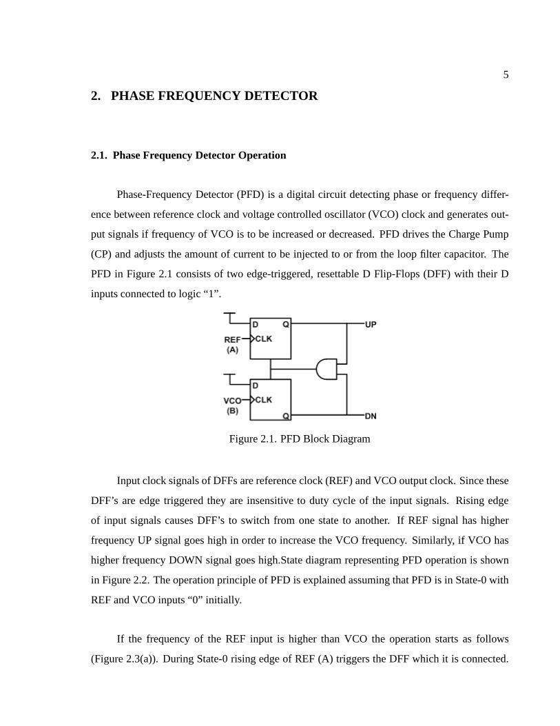
2. PHASE FREQUENCY DETECTOR
2.1. Phase Frequency Detector Operation
Phase-Frequency Detector (PFD) is a digital circuit detecting phase or frequency differ-
ence between reference clock and voltage controlled oscillator (VCO) clock and generates out-
put signals if frequency of VCO is to be increased or decreased. PFD drives the Charge Pump
(CP) and adjusts the amount of current to be injected to or from the loop filter capacitor. The
PFD in Figure 2.1 consists of two edge-triggered, resettable D Flip-Flops (DFF) with their D
inputs connected to logic “1”.
Figure 2.1. PFD Block Diagram
Input clock signals of DFFs are reference clock (REF) and VCOoutput clock. Since these
DFF’s are edge triggered they are insensitive to duty cycle of the input signals. Rising edge
of input signals causes DFF’s to switch from one state to another. If REF signal has higher
frequency UP signal goes high in order to increase the VCO frequency. Similarly, if VCO has
higher frequency DOWN signal goes high.State diagram representing PFD operation is shown
in Figure 2.2. The operation principle of PFD is explained assuming that PFD is in State-0 with
REF and VCO inputs “0” initially.
If the frequency of the REF input is higher than VCO the operation starts as follows
(Figure 2.3(a)). During State-0 rising edge of REF (A) triggers the DFF which it is connected.

6
Figure 2.2. PFD State Diagram
Data (D) inputs of DFF’s are connected to “1” thus UP switchesto “1”. Depending on the phase
difference of REF and VCO, rising edge of VCO (B) triggers thesecond DFF after a certain
amount of time. Then DN switches from “0” to “1”. At this pointboth inputs of the AND gate
is “1” and its output turns to “1” which activates reset signal for DFF’s. Reset signal generated
by PFD resets the DFF’s and outputs of both DFF’s return to “0”. Ideally DN signal should
never be “1”. However propagation of reset signal will require a finite time due to delay of AND
delay. Therefore DN signal will be seen as “1” for a very shorttime. The same sequence is valid
if VCO is faster than REF but in the opposite direction (Figure 2.3(b)).
(a) VCO slow (b) VCO fast (c) In-Phase (Locked)
Figure 2.3. Operation of PFD
If both VCO and REF have equal frequencies PFD will only generate short pulses. Time
required to reset the DFF’s mainly depends on the delay of thereset path. The width of short
pulses at PFD output as in Figure 2.3(c) is defined as minimum pulse width. To increase mini-
mum pulse width additional inverters can be added to AND gatein series. Thus the amount of
time that reset signal stays active and PFD stays longer in zero state.

7
This PFD detects frequency difference by comparing phases of input signals. Phase dif-
ference is detected by clock edges of input signals. According to this the output characteristic
of the PFD is shown in Figure 2.4. 0 degree phase difference corresponds to 0 Volt average. If
the phase difference is close to 2π then the output reaches to VDD assuming that output of PFD
between 0V and VDD. PFD gain is defined as,
KPFD =V DD
2π(2.1)
Figure 2.4. PFD characteristic
2.2. PFD Design and Simulation
The DFF’s of PFD can be built with different architectures. First one, based on NAND
gates in Figure 2.5(a); second one proposed in [2] is shown inFigure 2.5(b). First one has 2,3
and 4 input gates therefore the propagation delay of this type of DFF is larger. Second one has
two input gates and thus allowing short propagation delay and this result in short reset pulses
during lock condition.
The duration of minimum pulse width has an important effect on PLL. Very short reset
pulses result in dead-zone in charge pump causing non-linearity in PLL loop. On the other
hand very long reset pulses causes perturbation in output voltage due to any mismatch in charge
pump current. Also minimum pulse width is affected by operation temperature. As temperature
increases gates switch slower and minimum pulse width increases with increasing temperature.

8
(a) NAND based PFD (b) Branch based PFD
Figure 2.5. PFD models
Minimum pulse widths of PFD for three operation corners are listed in Table 2.1.
Table 2.1. Minimum pulse widths of PFD
Fast Typical Slow
Minimum Pulse Width (pS) 385 510 764
The outputs of PFD, UP and DN drive the charge pump switches. However, due to archi-
tecture of charge pump used the complements of outputs as UPBand DNB need to be generated.
To do this, UP signal is divided into two branches (Figure 2.6).
Figure 2.6. Output configuration to generate complementarysignals
First branch is composed of two inverters to regenerate UP signal. Second branch is com-
posed of one inverter and one transmission gate to generate UPB signal. The purpose of using
the transmission gate is to mimic the delay of first branch by loading the first inverter with ca-

9
pacitive load of the transmission gate. Unequal switching times of those signals cause mismatch
in charge pump output current increasing phase noise of PLL output. Using this additional
transmission gate will help the switching times of complementary UP and UPB signals match
better.
(a) PFD output without TG (b) PFD output with TG
Figure 2.7. Effect of transmission gate on output matching
In Figure 2.7(a) UP and UPB signals without the transmissiongate are shown. Rising
and falling edges of complementary signals intersect far from midpoint of supply voltage and
ground. The mismatch of two signals for two intersection points of rising and falling edges are
27ps and 36pS respectively. After adding the transmission gate intersection points of comple-
mentary signals are closer to mid Vdd as in Figure 2.7(b). Mismatch between intersection points
are reduced to 6ps and 12pS respectively.
While operation frequency increases the time which internal nodes of PFD stay around
mid-VDD is longer therefore PFD draws more current. Power dissipation of PFD versus oper-
ating frequency is plotted in Figure 2.8
Simulated operation modes of PFD are shown in Figure 2.9. First row demonstrates lock
state of PLL where reference input (REF) and clock input (VCO) are in same frequency and
in phase. Therefore PFD only generates reset pulses depending on the delay of the reset path.

10
Figure 2.8. PFD power dissipation versus frequency
In second row the frequency of clock input is higher than reference frequency and in every
cycle phase difference increases. In that case DN output haslarger duty cycle while UP has the
minimum pulse width. Similarly, in third row reference frequency is higher than clock frequency
and as a result UP has greater duty cycle to increase the operating frequency by charging the filter
capacitor.
Maximum operation frequency of PFD is 1 GHz. Therefore it canbe used with reference
clocks up to 1 GHZ frequency while using small divider valuesfor 2.5 GHz output frequency.
Since the reference input frequency PFD is 125 MHz, corresponding average power dissipation
for this operation frequency is 0.45 mW. PFD performance parameters are listed in Table 2.2.
Table 2.2. PFD Perfomance Summary
Performance Metric Value
Reference Frequency125 MHZ
Power Dissipation 0.45 mW
Max. Operation Freq. 1 GHz
Min Pulse Width 510 pS

11
Figure 2.9. PFD simulation for three modes of operation
12
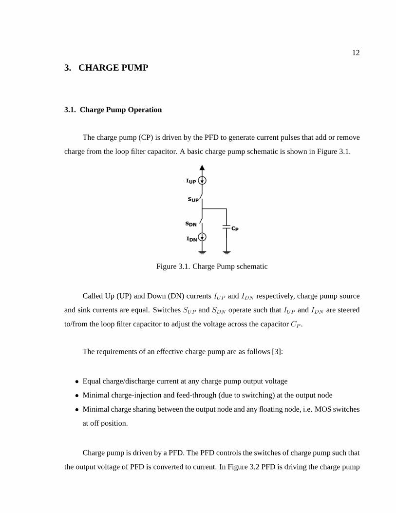
3. CHARGE PUMP
3.1. Charge Pump Operation
The charge pump (CP) is driven by the PFD to generate current pulses that add or remove
charge from the loop filter capacitor. A basic charge pump schematic is shown in Figure 3.1.
Figure 3.1. Charge Pump schematic
Called Up (UP) and Down (DN) currentsIUP andIDN respectively, charge pump source
and sink currents are equal. SwitchesSUP andSDN operate such thatIUP andIDN are steered
to/from the loop filter capacitor to adjust the voltage across the capacitorCP .
The requirements of an effective charge pump are as follows [3]:
• Equal charge/discharge current at any charge pump output voltage
• Minimal charge-injection and feed-through (due to switching) at the output node
• Minimal charge sharing between the output node and any floating node, i.e. MOS switches
at off position.
Charge pump is driven by a PFD. The PFD controls the switches of charge pump such that
the output voltage of PFD is converted to current. In Figure 3.2 PFD is driving the charge pump

13
where phase of A is leading phase of B. In that case PFD generates longer UP signals than DN
signals and voltage across capacitorCP increases.
Figure 3.2. PFD-CP Operation
In Figure 3.3 symmetric operation of charge pump with PFD is demonstrated. If PFD
orders the charge pump to charge the output capacitor, the voltage across the capacitor increases
in every cycle. Similarly voltage decreases with the same slope if phase difference is the same
but opposite. Voltage across the capacitor does not change if both of the switches are conducting.
When PLL is locked to the desired frequency phase differencebetween reference clock
and divided clock is zero. Therefore outputsQA andQB are expected to be equal to minimum
pulse width. If the phase difference is very small then the pulse width of related output is
close to minimum pulse width. MOSFETs require minimum time of logic “1” on their gates
to start conducting current between drain and source because of finite gate capacitance. If the
pulse width of PFD is not long enough to open switches of charge pump small phase difference
cannot be corrected by charge pump.
This non-linear behavior of charge pump is defined as dead zone. Dead-zone region of a
charge pump is shown in Figure 3.4. If the input phase difference is belowφo then the voltage
around output capacitor is not a function of∆φ. In dead-zone region no current is injected to

14
Figure 3.3. Charge Pump charging and discharging output capacitor
output capacitor and PLL is not locked causing VCO to accumulate random phase error. This
random variation of the output clock in time domain is calledas jitter.
Figure 3.4. Charge Pump dead zone
In order to deal with dead zone, the pulse width of PFD output should be widened by
increasing the reset delay of PFD. The delay in reset path of PFD can be increased by adding
inverters as delay elements therefore charge pump switchescan switch to conduction. Thus any
small amount of phase difference can be detected by charge pump. However increasing mini-
mum pulse width causes charge pump to short circuit while both of the switches conduct current

15
and perturbating the voltage around output capacitorCP . This perturbation can be reduced by
the loop filter therefore increasing minimum pulse width is areasonable choice to eliminate
dead-zone. The important point is to adjust minimum pulse width long enough to eliminate
dead zone but not too long for avoiding any mismatch related phase errors.
3.2. Charge Pump Design and Simulation
In previous section it is stated that charge pump currents UPand DN should match each
other. Voltage across the output capacitor changes between0.5V and 1.2V, those currents should
not be affected by output voltage of current sources. This requires high output resistance there-
fore using cascode structure for current sink and current source is a reasonable choice. A High-
swing low voltage cascode current source reference [4, p274] is used to generate the bias volt-
ages of the current source (Figure 3.5). Similarly, the PMOScurrent sink is biased with the same
reference.
Figure 3.5. High swing low voltage cascode reference
The reference is composed of two branches to reduce the inputvoltage enabling current
reference to be used with low voltage power supplies. Because M1 and M2 is biased in saturation

16
region the output resistance is same with cascode current source defined as,
Ro = gm(2)rds(2)rds(1) (3.1)
M5 operates as a bias transistor for M6 such that M5 and M6 can be collapsed into one transistor
and replaced by M7 and M7 is sized by a factor of four or less then the aspect ratio of M3 and
M4 to satisfy the bias conditions of the circuit. Actual ratio between aspect ratios of M7 and
M3/M4 is 1/11.
Charge pump circuit works over a wide temperature range and different process corners
as well as other PLL components. Current matching is a critical issue in charge pump. A beta
multiplier current reference is sensitive to temperature and process variations. In order to avoid
those variations a bandgap based current reference is used [5] as in Figure 3.6. The voltage
across the resistor is constant and equal to bandgap reference voltage. An amplifier adjusts
gate voltage of the PMOS continuously ensuring that the voltage across the resistor is equal to
bandgap reference voltage. Bias current depends on variation of the resistance of the resistor.
Using a high resistivity poly resistor enables one to generate reference current that does not vary
much with temperature because of its small temperature constant [6].
Figure 3.6. Bandgap based current reference for charge pump
Feedback is involved in amplifier configuration so stabilityof the amplifier should also be

17
considered. The response of the amplifier to 1.2V step input is shown in Figure 3.7. Stability
can be improved by adding a capacitor and a resistor in seriesat the output of the amplifier.
Figure 3.7. Transient response of reference circuit
There are different non-idealities involving charge pumps. A charge pump schematic is
shown in Figure 3.8(a). If switches S1 and S2 are OFF, the parasitic capacitance seen at the drain
of M1 is discharged to GND and parasitic capacitance of M2 is charged to VDD. In next cycle
of PFD switches S1 and S2 start conducting and voltagesVX , VY settles to voltage of output
capacitorVcont. However the voltage difference betweenVcont andVX can be more or less than
the difference betweenVcont andVY (Figure 3.8(b)). The difference between those voltages is
supplied byCP perturbating output voltage defined as charge sharing [7, p566]. Charge-sharing
is expected to be more dominant when PLL is locked because charge pump switches is not
conducting for most of the PFD cycle.
In order to deal with charge sharing between those capacitances a method proposed in [8]
is used. Charge pump is divided into two paths and the output voltage is buffered to the other
path by a unity gain amplifier (Figure 3.9).

18
(a) (b)
Figure 3.8. Charge sharing in charge pump
Figure 3.9. Charge Pump with a unity gain amplifier

19
The unity gain amplifier connects the floating nodes to outputvoltage so that those nodes
stay at the same voltage with output voltage. The differencebetween those nodes and output
voltage is reduced and charge sharing is minimized allowinga stable output voltage.
Charge pump’s UP and DN currents must match each other while output voltage changes.
Mismatch due to channel length modulation can be avoided by cascode current source with large
output impedance. The output impedance of current sink and source is up to 500 MΩ. Since
cascode current source and sink consist of low voltage cascode configuration they can operate
with approximately twoVDS(sat)s allowing large headroom for output voltage. Large output
headroom enables wide range of operation region of charge pump which is defined as linear
region of charge pump. The linear region of charge pump is plotted in Figure 3.10.
Figure 3.10. Charge pump linear operation region
Linear region of charge pump is defined where difference between UP and DN currents
is zero ideally. However there is a small mismatch between those two due to process and tem-

20
perature variations. Nominal charge pump current (ICP ) and mismatch between UP and DN
currents at the center of charge pump’s linear region for three process corners are shown in Ta-
ble 3.1. Compared to nominal currentICP , current mismatch is relatively small but it contributes
to phase offset of PLL.
Table 3.1. Charge pump currents and mismatch in corners
Fast Typical Slow
Current Mismatch (nA) 3.00 1.40 1.58
Charge Pump Current (µA) 9.48 10 11
Other issues related with charge pump are charge injection and clock feed through. When
a MOSFET is conducting current a channel exists at the oxide-silicon interface. Proportional to
the channel length charge in channelQCH is accumulated in the inversion layer. When the switch
is turned offQCH exits through source and drain terminals, a phenomenon called “channel
charge injection”.
Figure 3.11. Effect of channel charge injection
Shown in Figure 3.11, the charge injected to the left is absorbed by input source creating
no error. However the charge injected to the right is absorbed by output load introducing an
error in the output voltage.
In addition to charge injection a MOSFET switch couples clock transitions to the output
capacitor through its gate drain or gate source overlap capacitance shown in Figure 3.12. This
phenomenon is called as “clock feedthrough”.

21
Figure 3.12. Clock feedthrough in a MOSFET
Error in the output voltage due to clock feedthrough is expressed by,
∆V = VckWCOV
WCOV + CH
(3.2)
To overcome error at the output caused by clock feedthrough,dummy switches are connected to
output nodes of the charge pump [7, p421]. Dummy switches’ drain and source junctions are
short circuited so thatCgs andCgd capacitances of those are connected to output while onlyCgd
capacitance of master switches are connected. Therefore dummy switches are sized as half of
master switches to generate same amount of charge.
For charge injection, NMOS master switches have PMOS dummy switches and PMOS
master switches have NMOS dummy switches. NMOS switches inject electrons and PMOS
switches inject holes to the output so that they complement each other. This helps to cancel
injected charge with its complement. Charge pump schematicwith dummy switches is shown
in Figure 3.13. Since dummy devices are complements of master devices their clock sources are
also complements of master switches.
Table 3.2 lists the charge-pump parameters for typical operation. Linear region for output
voltage is between 0.6V and 1.2V with a charge pump currentICP =10µA.

22
Figure 3.13. Charge pump with dummy switches
Table 3.2. Charge Pump Summary
Performance Metric Value
Charge Pump Current (ICP ) 10µA
Linear Region 0.6V - 1.2V
Max. Mismatch 3 nA

23
4. VOLTAGE CONTROLLED OSCILLATORS
4.1. Integrated Oscillators
4.1.1. Oscillation Principles
An oscillator forms a periodic output, generally in the formof voltage. Although there is
no input, an oscillator sustains the output indefinitely. Transfer function of feedback system in
Figure 4.1 is defined by,
Vout
Vin(s) =
H(s)
1 + H(s)(4.1)
Figure 4.1. Feedback System
An oscillator is an amplifier which experiences so much phaseshift at higher operating
frequencies thus overall feedback becomes positive and oscillation may occur. Definings =
jωo, if H(jωo) = −1 closed-loop gain becomes infinite. A noise component atωo experiences
a gain of unity and a phase shift of180o, returning to the subtractor as a negative replica of the
input, and that corresponds to0o or 360o total phase shift. Consequently the component atωo
continues to grow. Named as “Barkhausen Criterion” a negative feedback loop gain satisfies
these two conditions for oscillation:
|H(jωo)| ≥ 1 (4.2)

24
∠H(jωo) = 180o (4.3)
A loop gain at least two or three times greater than unity is necessary to ensure oscillation against
temperature and process variations.
(a) (b)
Figure 4.2. Representation of positive feedback
Figure 4.2(a) it is seen that the circuit has already a phase shift of 180o because of negative
feedback. Therefore (4.3) states that an additional180o frequency dependent phase shift is
required for oscillation. This configuration can be represented in Figure Figure 4.2(b).
4.1.2. Types of Integrated Oscillators
Oscillators are defined as autonomous circuits that generate periodic signals. They have
at least two states and they cycle through these states at a constant frequency. The three types of
integrated oscillators are: 1) LC Oscillator 2) Ring Oscillator and 3) Relaxation Oscillator.
Ring oscillators consist of an odd number of single-ended inverters or an even/odd number
of differential inverters with appropriate connections. Relaxation oscillators alternately charge
or discharge a capacitor with a constant current between twothreshold levels. Resonant based
circuits such as LC VCOs are another type of oscillator structures.
Noise analysis and design techniques of LC VCO is well developed and understood in
literature and they are known to have excellent jitter performance. Compared with ring VCOs,
LC VCOs have superior phase noise performance. Besides, recent research indicates that phase

25
noise performance of ring VCO and LC VCO is comparable in deepsubmicron process en-
abling to use ring VCOs in many circuits. Also wide tuning range, design simplicity and cost
effectiveness makes ring VCO a good choice against LC VCO [9].
4.2. CMOS Ring Oscillators
4.2.1. Ring Oscillator Basics
Ring oscillator consists of a number of gain stages in a loop.Before starting with ring
oscillator consider a single stage inverter and common source amplifier with unity gain feedback.
(a) single stage inverter (b) single stage CS ampli-
fier
Figure 4.3. Single stage inverter and amplifier
In Figure 4.3(a) a single stage inverter can also be represented as a common source am-
plifier as in Figure 4.3(b). Single stage inverter has a single dominant pole due to its output
capacitance and frequency dependent phase shift is−90o at infinite frequency. A−180o DC
phase shift comes from the negative feedback which results with a total phase shift of−270o.
Circuit does not establish “Barkhausen Criterion” even at infinite frequency therefore oscilla-
tion does not start. If an additional inverter added to single stage inverter as in Figure 2.4 there
exist two poles which brings−180o frequency dependent phase shift. In this configuration total
DC phase shift is0o and maximum frequency dependent phase shift is−180o. Therefore total
maximum phase shift is180o. In that case circuit latches-up. IfV1 increasesV2 decreases which

26
causesV1 to increase more. This continues untilV1 andV2 up to VDD and GND respectively.
As a result circuit stalls rather than it oscillates.
Figure 4.4. Two stage inverter
Figure 4.5. Three stage inverter
Even number of inverters results fails to oscillate thus a third inverter stage is added to
previous circuit introducing a third pole on signal path (Figure 4.5). Total phase shift around the
loop is−135o at ω = ωp whereωp is 3dB bandwidth of inverter stages. Maximum frequency
dependent phase shift is−270o at ω = ∞ and total phase shift equals−180o at ω < ∞ which
is a finite frequency. If loop gain is greater than 1 at the point where frequency dependent phase
shift 180o and total phase shift is360o, oscillation starts. Frequency dependent phase shift of
three stages is180o at oscillation frequency therefore identical stages bring60o phase shift.
Oscillation frequency of a ring oscillator is defined by,
Fout =1
2Nτd
(4.4)
where N is the number of stages andτd is the delay of a single ring oscillator stage.

27
4.2.2. Single Ended Ring Oscillator
A simple single ended ring oscillator schematic in Figure 4.6 consists of CMOS inverters.
To ensure oscillation, single-ended topology is used with an odd number of inverters.
Figure 4.6. Three stage ring oscillator
Current is consumed in CMOS inverters during transition instances while output capaci-
tances are charged and discharged. In inverters with current source or current sink, the amount
of current is determined by tail current source or current sinks. A lower amount of current would
result with a longer transition due to longer charge/discharge duration of output capacitance. The
current which flows through the tail current source or sink iscontrolled by bias voltage which
is named as VCO control voltage. VCO control voltage controls the current flow therefore the
frequency of oscillation.
A single ended inverter topology with tail current source and current sink is shown in
Figure 4.7. Ring oscillator circuit consists of three current-starved inverters is called as current-
starved ring oscillators. This configuration is highly non-linear and has an extremely limited
operating range.
Output frequency of an oscillator can be controlled with capacitive tuning. Capacitive tun-
ing is based on adjusting the output capacitance of an inverter by a voltage-dependent capacitor
for example a reverse biased p-n junction diode as in Figure 4.8(a). Also in Figure 4.8(b) using a
MOS device operating as a voltage-dependent resistor changes effective capacitance seen at the
output node. This single-ended delay control methods are susceptible to common-mode noise
as well as other single-ended circuits. Also considerable amount of variation inKV CO makes

28
Figure 4.7. Current-starved inverter
capacitive tuning difficult to apply for a wide tuning range.In contrast to capacitive tuning,
resistive tuning provides relatively wide and uniform variation in frequency besides allowing
diffential control [1].
(a) with adjustable capacitor (b) with adjustable resistor
Figure 4.8. Capacitive tuning
4.2.3. Differential Ring Oscillator
Ring oscillators can be single-ended or differential. Differential ring oscillator is built with
differential inverters those have a load and NMOS or PMOS input differential pair. The delay of
inverter is determined by the time time constant of the output node. Differential ring oscillators
may have odd or even number of inverter stages.

29
Figure 4.9. Differential Ring Oscillator
If even number of stages are used the output of one stage is cross connected to the fol-
lowing stage as in Figure 4.9. Therefore positive feedback is ensured for oscillation frequency.
By using even number of inverters in ring oscillator, for example four stages, quadrature clocks
can be generated. Compared to single ended delay stage, differential stage have much better
common-mode noise rejection like supply noise and substrate noise. Differential ring oscilla-
tors have a lower noise injection into other circuits on the same chip because of constant current
flowing through their tail transistor.
Differential pair can consist of in different types loads for resistive turning. PMOS load
devices in Figure Figure 4.10(a) are biased in triode regionand their resistance is adjusted by
Vb. As Vb decreases, the delay of the stage is reduced because time constant at the output node
decreases. However, the small signal gain of the circuit also decreases. As the loop gain of falls
below unity the circuit consequently fails to oscillate. InFigure 4.10(b), although small signal
impedance of PMOS load changes as tail current changes, the voltage gain remains constant.
But signal output voltage still depends on output current. In Figure 4.10(c) delay stage based on
symmetric load elements based on source-coupled pair composed of a diode connected PMOS
and biased PMOS in parallel.
With the output swings referenced to the top supply NMOS current source isolates the
buffer from the negative supply so buffer delay remains constant with supply voltage. Because
they have symmetric I-V characteristic around the center ofvoltage swing they are called as sym-
metric load elements. Symmetric loads are substantially reducing the jitter caused by common-

30
(a) triode load (b) diode load (c) triode with diode load
Figure 4.10. Differential delay stage with different load types
mode noise present on the supplies. Because of those advantages symmetric loads are used in
this PLL design.
4.3. Noise Sources
Noise is the unwanted signal that affects the performance ofa system. It degrades the
performance of a system such as maximum operating speed of a clock generator. Major charac-
teristic of noise is its randomness which is due to physical effects which generate noise. Noise
is divided into two categories as Interference Noise and Inherent Noise.
Interference noise is based on the interaction of circuit between other circuits, peripherals
or power supply. It may or may not be random signals. Inherentnoise is depends on properties
of devices. It is a random noise. It can be reduced by circuit and layout techniques but it cannot
be eliminated. Inherent noise sources are divided into two categories, ultimate and excess noise,
according to their origin. Ultimate noise sources are defined as thermal and shot noise that they
derive from the physics of materials and not the quality of the devices. Therefore they cannot be
suppressed but optimized. Flicker and popcorn noise are defined as excess noise sources because
they depend on the quality of the components such as cleanness of the gate oxide surface. Most

31
common noise types thermal noise and flicker noise are explained as follows.
4.3.1. Thermal Noise
Thermal noise is due to random motion of electrons (carriers) in a conductor which in-
troduces randomly varying current causing fluctuations in the signal measured around the noise
source. The power spectrum density is uniform at all frequencies as in Figure 4.11. Since flicker
noise spans all frequency range it is also called “white noise”.
Figure 4.11. Spectrum of Thermal Noise
4.3.2. Flicker Noise
The interface between the gate oxide and silicon substrate in a MOSFET has many defec-
tive bonds. As charge carriers move at that interface some are randomly trapped and released,
generating flicker noise in current. Depending on the cleanness of the oxide-silicon interface
flicker noise may vary from one CMOS technology to another. Flicker noise is always associ-
ated with a direct flow of current and has a power spectral density is shown in Figure 4.12.
Figure 4.12. Spectrum of Flicker Noise

32
It is apparent that flicker noise is most significant at low frequencies and reduces in ampli-
tude as frequency increases. Although device exhibit high flicker noise levels at low frequencies
flicker noise may dominate the device noise at frequencies well into the megahertz range.
4.4. Phase Noise
Noise injected into an oscillator by interference or inherent noise sources may influence
both the frequency and amplitude of output signal. In most cases disturbance in output is neg-
ligible or unimportant, and the random deviation of the frequency is considered. Frequency
deviation can be viewed as random variation in period or deviation from the zero crossing points
from their ideal position along the time axis. The output of apractical oscillator is defined by,
x(t) = Acos(ωct + φ(t)) (4.5)
Whereφ(t) is small excess phase representing variations in period. The functionφ(t) is called
“phase noise”. For —φ(t) 1—, Vout(t) = Acos(ωct−Aφ(t)), which means that spectrum of
φ(t) is translated to±ωc [10].
Figure 4.13. Effect of phase noise on an oscillator
Phase noise is usually characterized in the frequency domain. For an ideal sinusoidal
oscillator operating atωc, the spectrum assumes the shape of an impulse, whereas for anthe
spectrum exhibits “skirts” around the carrier frequency (Figure 4.13)
Phase noise arises from random frequency components. To quantify phase noise, a unit
bandwidth of 1 Hz at an offset∆f from the carrierωc (Figure 4.14) is defined to calculate the

33
noise power in that unit bandwidth and divide the result by the carrier power. The carrier power
is defined as the total area under the curve.
Figure 4.14. Phase noise calculation around the carrier
L∆f = 10logPside(fo + ∆f, 1Hz)
Pc(4.6)
Pside(fo+∆f, 1Hz) represents the sideband power in 1 Hz bandwidth atf = fo +∆f and
Pc represents the carrier power. Phase noise is expressed in terms of dBc/Hz and “c” indicates
normalization of noise power to the carrier power and Hz identifies the unity bandwidth used
for the noise power.
The effect of phase noise can be easily understood with a wireless receiver [11]. In
a receiver, a local oscillator (LO) is used for downconverting high frequency signals (Fig-
ure 4.15(a)). The LO output (Figure 4.15(b)) and the desiredsignal is multiplied by a mixer,
and shifted to baseband. However, there are other unwanted signals present, which are also
downconverted. If the LO output is noise-free, then the mixer output spectrum will be the one in
Figure 4.15(c). However, if the LO output is corrupted by phase noise (Figure 4.15(d)), then the
mixer output spectrum will be the one in Figure 4.15(e). The output spectrum consists of two

34
(a)
(b)
(c)
(d)
(e)
Figure 4.15. Effect of phase noise on a reciever

35
overlapping spectra. And if the unwanted signal in the adjacent channel has a large power level,
the wanted signal terribly suffers from significant noise due to the tail of the interferer.
The counterpart of phase noise in time domain is called as jitter. Jitter is defined as vari-
ations in zero crossings of a signal from the ideal position as shown in Figure 4.16. Expected
crossing timings in a signal never occur exactly where desired. The accuracy of those crossings
is critical to the performance of communication systems in order to obtain proper data sampling
timings.
Figure 4.16. Effect of jitter on clock edges
4.5. Ring VCO Design and Simulation
The VCO block in consists of three stage differential mode delay cells with a voltage-
to-current converter circuit (V2I) and an output buffer (Figure 4.17). V2I circuit is used to
convert VCO control voltage to a bias current for differential mode delay cell stages. Output
buffer shifts the output of three-stage VCO and converts thedifferential signal to single ended
output. Finally, inverter chain of output buffer converts the single ended output of previous part
to rail-to-rail signal for CMOS operation.
VCO contributes to most of the phase noise at the output of PLLtherefore phase noise of
VCO design is taken into consideration. As previously mentioned phase noise is simply defined
as the noise skirts around an ideal operating frequency. Lowfrequency noise sources are major
contributors of phase noise especially flicker noise. The dominant flicker noise sources are bias

36
Figure 4.17. VCO block diagram
and frequency control circuits instead of the devices in thedelay cell. In a fully differential ring
oscillator low-frequency noise close to DC from the bias circuit and tail devices is up-converted
around the carrier frequency by frequency modulation.
Figure 4.18. N-Stage ring oscillator with bias stage
A simplified schematic of a N-stage voltage controlled oscillator with bias circuitry is
shown in Figure 4.18. The noise from the bias transistor Mb isseparate from the noise con-
tributed by tail transistors of delay stages because the lowfrequency noise from Mb is correlated
for all stages while noise from tail transistors is not. Considering the noise contribution of the
bias device Mb, the noise power is amplified bym2 times by each tail device. In practice, the
flicker noise from could be the major noise source at low offset frequencies [12].
In this VCO representation there is only a single device (Mb)included in the bias. In
reality, more devices are often used for the bias. For example, a voltage-to-current converter
(V2I) is usually needed between the loop filter and the VCO in aPLL. Any low-frequency

37
noise generated inIctrl is equivalent to an increase in the noise from Mb and could potentially
dominate the low-frequency phase noise. According to the basis for phase noise contribution
of bias circuitry additional components such as V2I is addedand schematic of bias circuit with
V2I block is shown in Figure 4.19.
Figure 4.19. VCO V2I circuit
Reducing flicker noise of V2I block is helpful on phase noise performance therefore one
should be aware of flicker noise behavior of MOSFETs. Charge trapping phenomena are usu-
ally used to explain 1/f noise in MOSFETs. Since MOSFETs are surface devices defects and
impurities of surface and interface can randomly trap and release charge. Larger MOSFETs
exhibit less 1/f noise because their larger gate capacitance smoothes the fluctuations in channel
charge. Therefore to obtain good 1/f performance large practical devices are used [13, p.254].
According to this information the length of MN1 of bias circuit is chosen to be 4µm. The length
of MN2 is 0.7µm which has the same length of tail transistor of delay cells.Simulation results
verify that 75 per cent of noise in VCO is generated from MN1 indicating the importance of
noise contribution of bias circuit. Table 4.1 shows the device dimensions of V2I circuit.
It is mentioned that the noise power of bias device is amplified by m2 times by each tail
transistor. To reduce the noise contribution of that kind, the currents of devices MN1 and MN2
are equal to the tail device currents of delay cells. The current scaling ratiom is equal to 1 and
noise contribution of bias circuit is no more multiplied by square of scaling ratio.

38
Table 4.1. Device dimensions of V2I circuit
Device W (µm) L (µm)
MN1 140 4
MN2 150 0.7
MP1 90 0.36
MP2 52 0.22
Second issue on designing the bias circuit is VCO control voltage (Vctrl) range. The oscil-
lation frequency depends on the tail transistor current. Current of devices operate in saturation
region is defined by,
I =µCox
2Abulk
W
L(VGS − VT )2 (4.7)
showing that tail current therefore operating frequency changes with overdrive voltageVGS−VT
with a quadratic dependence. Considering loop dynamics linear dependence of VCO frequency
with respect to control voltage is desired. Using a wide device for MN1 with a resistor connected
to its source keeps the overdrive voltage of MN1 at a small value causing the current of this
device linearly with gate voltage [14]. However additionalthermal noise contribution of resistor
connected to bias circuit will degrade the noise performance. Thus only a wide NMOS device
is used without a resistor connected to its source.
The maximum value of control voltage prevents MN1 to remain in saturation due to volt-
age drop on MP1 and maximum ofVctrl is chosen to be 1.05V for worst case situation which
corresponds to125o temperature with slow corner process parameters.
The delay cell in Figure 4.20, contains NMOS source coupled-differential pair and sym-
metric loads which provide good control over delay and high dynamic supply noise rejection.
With the output swings referenced to top supply, the tail current source effectively isolates the
buffer from negative supply so that the buffer delay remainsconstant with supply voltage. Load

39
Figure 4.20. Delay cell with symmetric loads
elements are composed of a diode connected PMOS device parallel with a biased PMOS device
with equal size. They are called symmetric loads because their I-V characteristic is symmetric
around the center of voltage swing [15].
Bias voltage of PMOS device (Vbp) is obtained from the gate ofPMOS device MP1 of the
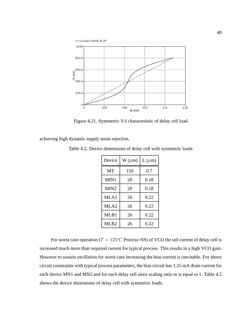
VCO bias circuit. The simulated I-V characteristic of symmetric load is shown in Figure 4.21.
The lower swing limit is symmetrically opposite at the bias level of Vbp. The dashed line
represents the effective resistance of symmetric load. Since voltage swing depends on Vbp, if
the buffer bias current is adjusted the output swings vary with the control voltage rather than
being fixed in order to maintain the symmetric I-V characteristics of the loads.
Linear resistor loads are most desirable for achieving highdynamic supply noise rejection.
Because they provide differential-mode resistance that isindependent of common-mode voltage
carrying the supply noise, the delay of the buffers is not affected by common-mode noise. Unfor-
tunately, adjustable resistor loads made with real MOS devices cannot maintain linearity while
generating a broad frequency range. Symmetric loads, though nonlinear, can also be used for
40
Figure 4.21. Symmetric V-I characteristic of delay cell load
achieving high dynamic supply noise rejection.
Table 4.2. Device dimensions of delay cell with symmetric loads
Device W (µm) L (µm)
MT 150 0.7
MIN1 20 0.18
MIN2 20 0.18
MLA1 26 0.22
MLA2 26 0.22
MLB1 26 0.22
MLB2 26 0.22
For worst case operation (T = 125oC Process=SS) of VCO the tail current of delay cell is
increased much more than required current for typical process. This results in a high VCO gain.
However to sustain oscillation for worst case increasing the bias current is inevitable. For above
circuit constraints with typical process parameters, the bias circuit has 1.25 mA drain current for
each device MN1 and MN2 and for each delay cell since scaling ratio m is equal to 1. Table 4.2
shows the device dimensions of delay cell with symmetric loads.

41
Output buffer of VCO in Figure 4.22 consists of a low swing buffer, dual differential
amplifier with differential to single ended converter (D2S)and chain of inverters. The functions
of those blocks are as follows.
Figure 4.22. VCO output buffer block diagram
First part of VCO output buffer is a low-swing low gain differential buffer shown in Fig-
ure 4.23. Its purpose is to isolate the last stage of the ring oscillator from the following amplifier
stage. Amplifying the output of third delay cell will increase the capacitance seen at the output
of VCO due to miller effect thus degrading the oscillation frequency.
Figure 4.23. Low-swing buffer
Second part of VCO output buffer is dual differential amplifier with D2S which amplifies
the low-swing output of the previous buffer stage (Figure 4.24). It is used to increase the voltage

42
swing of low-swing buffer output and convert the differential output to single ended output.
Figure 4.24. Differential to single-ended converter
Dual differential amplifiers ensure the symmetric loading of low-swing amplifier. Single
differential amplifier has one PMOS load diode connected andother one is biased with the gate
voltage of diode connected PMOS. If a single differential amplifier is used, the capacitance seen
from the inputs will be different because diode connected PMOS will bring more capacitance
to drain junction of input transistor. For symmetric operation an additional differential amplifier
is connected with opposite phase inputs. Thus both outputs of low-swing buffer see equal input
capacitance and differential output signals are equal in amplitude.
Differential to single ended converter (D2S) is composed offour PMOS common source
amplifiers. Those common source amplifiers are biased from the output of dual differential
amplifiers. Same as the previous stage outputs of dual differential amplifiers are interchanged to
the inputs of PMOS common source amplifiers. Common source amplifiers provide additional
signal amplification and conversion to a single ended outputthrough the NMOS current mirror
[16]. Input transistors of common source amplifiers are PMOStransistors thus the signal level
of differential amplifiers should provide enough overdrivevoltage.
Last stage of the VCO buffer consists of 8-stage inverter chain which converts the ampli-
fied single-ended signals to rail-to-rail output for CMOS operation (Figure 4.25).

43
Figure 4.25. 8-Stage inverter chain
Also considering Logical Effort, the inverters are sized such that last inverter can drive
large capacitive load with minimum delay. A short tutorial on Logical Effort is given in Appendix-
A. The total current drawn from power supply by VCO includingthe output buffer is 18.5 mA
which corresponds to a power consumption of 33.3 mW.
The frequency characteristic versus frequency curve for three process corners is shown in
Figure 4.26. The gain of the voltage controlled oscillatorKV CO for typical process is 7 GHz/V,
for slow corner 3.8 GHz/V and for fast corner 10 GHz/V.
Figure 4.26. VCO frequency versus control voltage

44
The DC characteristic of a delay cell is shown in Figure 4.27.Open-loop gain of a single
delay stage is close to 10 satisfying oscillation criteria (4.2) for three-stage VCO.
Figure 4.27. DC characteristic of delay cell
The outputs of VCO and internal nodes of VCO output buffer is shown in Figure 4.28(a),
4.28(b), 4.28(c), and 4.28(d). Figure 4.28(a) shows the output of three-stage VCO, with an
output swing of 0.7V. In Figure 4.28(b) the output of VCO is shifted to a DC level close to mid
VDD and as a result of low gain amplifier with diode connected PMOS loads output swing is
reduced to 0.3V.
In Figure 4.28(c) single ended output of D2S is plotted. It isimportant that single ended
output swing must be symmetric and large enough to ensure proper input for inverter chain.
Threshold of first inverter may vary with temperature and process corners and inverter chain
may fail to convert single ended output to rail-to-rail leading constant output at VDD or GND
level.
In Figure 4.28(d) output of inverter chain is shown. Duty cycle of output signal may vary
due to process and temperature variation however using the D2S enables duty cycle to stay in
reasonable limits. For all corners maximum variation of duty cycle is 5 per cent.

45
(a) 3-Stage ring oscillator output (b) Low-swing buffer output
(c) D2S output (d) Inverter chain output
Figure 4.28. Consecutive outputs of VCO

46
Phase noise plot of VCO is shown in Figure 4.29. The phase noise at 100 kHz offset from
the center frequency is -58 dB. Since the phase noise of VCO isthe most dominant noise source
in PLL the simulation data is going to be used in closed loop noise analysis of PLL.
Figure 4.29. Phase Noise of VCO

47
5. FEEDBACK DIVIDER
Feedback dividers are used to divide the output frequency and establish the multiplication
ratio of PLL. If divider ratio is N then the output frequency is divided by N and divided signals
is compared with reference frequency by PFD (Figure 5.1).
Figure 5.1. Frequency multiplication in PLL
In that case output frequency is defined as,
Fout = FinN (5.1)
There are fixed ratio dividers and programmable dividers. First one is used to generate out-
put frequency with fixed reference frequency. If a programmable divider is used the reference
frequency can vary depending on allowable division ratios to generate desired output frequency.
If the output frequency of a PLL is high, the divider may not befunctional due to required
operation speed. For example, to divide 2.5 GHz output frequency NAND based DFF’s speed
is not enough for operation. Before the divider a fast prescaler can be used to divide the output
clock however it is not useful to add too many prescaler stages after input of divider because
jitter increases after every logic stage due to their noise contribution. Even using a fast TSPC
[17] based prescaler with a division ratio of 4, NAND based programmable divider still failed
to operate at 625 MHz for slow corner parameters. Also using afixed prescaler limits the pro-
grammable division ratio because it already has a fixed division ratio before the programmable

48
divider. Thus a CML based programmable divider topology is used to achieve high speed oper-
ation with programmable division ratios.
The programmable divider architecture in Figure 5.2 is composed of 2/3 divider cells
connected like a ripple counter. The different cells of the divider are based on similar topology
therefore it facilitates layout work [18].
Figure 5.2. Programmable divider with 2/3 cells
The operation of the divider is as follows. Once themodn−1 signal is generated in a
division period, the signal propagates to the left by being reclocked by each cell along the way.
If the programming bit “p” of 2/3 cell is set to “1” then the modsignal enables the cell to divide
by 3. Division by 3 adds one extra period of input signal to theoutput signal. Thus a chain of
divider with 2/3 cells have an output signal with an output period,
Tout = 2nTin + 2n−1Tinpn−1 + 2n−2Tinpn−2 + ... + 2Tinp1 + Tinp0 (5.2)
which can be written as,
Tout = (2n + 2n−1pn−1 + 2n−2pn−2 + ... + 2p1 + p0)Tin (5.3)
whereTin is the period of input frequencyFin andpn is the programming bit of the 2/3 cell. The
equation shows that division ratios start from2n.
Logic implementation of 2/3 Cell is based on two functional blocks as shown in Figure 5.3.

49
Prescaler logic block divides the input signal with controlof end-of-cycle logic either by 2 or 3
and outputs the divided clock to next cell in chain. End-of-cycle logic determines the division
ratio continuously depending on modin and p signals. The modin signal is active once in a
division cycle and at that time the state of the “p” input is checked. If p=1 then the end-of-cycle
logic forces the prescaler to swallow extra one period. Otherwise divider stays in divide-by-2
mode. Regardless of the operation mode with respect to “p”, end-of-cycle logic reclocks the
modin signal and propagates it to the left cell in the chain.
Figure 5.3. 2/3 divider cell schematic
Circuit implementation of 2/3 Cells are based on Current Mode Logic (CML) logic blocks.
CMOS gates have very small static power dissipation assuming that leakage current to be small.
However for high speed operation CMOS gates suffers from some drawbacks. Using PMOS
transistors degrades maximum operating frequency due to its low mobility. Like any single
ended circuit CMOS gates is susceptible to supply and substrate noise and crosstalk. For very
high operation frequencies CML has lower power dissipationthan CMOS logic. Besides CMOS
gates dynamically generate large current flow from supply toground and this large amount of
current generate a noise may cause crosstalk between digital and analog circuitry [19].

50
Logic blocks of 2/3 Cell based on CML is shown in Figure 5.4. Figure 5.4(a) represents
D-Latch and Figure 5.6(b) represents a latch combined with an AND function to implement the
logic operation of the delay cell.
(a) CML Latch (b) CML Latch with AND function
Figure 5.4. CML blocks
The design method of CML latch proposed in [20] is followed for sizing the transistors.
Shown in Figure 5.5, a CML latch drives another CML latch. Total load associated with the
output of CML latch is parasitic capacitance at the drain of input transistor with an additional
gate and drain junction capacitance of memory block of the latch and the input capacitance of
next latch. Therefore first approach is to minimize the length of all transistors to minimum size
allowed by technology thus minimizing parasitic capacitances.
Rest of the design is based on choosing load resistance (R), tail current and widths of all
transistor pairs in the circuit. Design constraints are output capacitance, voltage swing and input
frequency. The voltage swingVsw is defined by,
Vsw = 2IbiasR (5.4)

51
Figure 5.5. CML Latch design model
The gain of memory cellAv(mem) should be greater than unity for proper operation. Since
both memory cell and input differential pair operate with same bias current the gain of input
differential pairAv is chosen to be same asAv(mem). Av = Av(mem) implies thatWin=Wmem.
Although a ratio of 1 to 5 forWck/Win is tolerable,Wck=1.25Win is a reasonable choice for
a robust design and low input capacitance. For determining the tail current all process corners
are concerned. A complex capacitance model is introduced inproposed method thus in order
to simplify this design step, a tail current of 200µA is approximated from reference designs
and used as initial estimation. After a few iterations for a 0.6V voltage swing, resistance R is
determined as 2kΩ from (5.4) while2Ibias = 300uA. OnceWin is determinedWmem andWck
is also determined from the above given ratios. The circuit parameters are as follows;
Win = 3.2µm
Win = 4µm
R = 2kΩ
2Ibias = 300µA
CML outputs for divide-by-2 and divide-by-3 operation for 2.5 GHz input signal is plotted
in Figure 5.6(a) and Figure 5.6 respectively. In divide-by-2 operation the program bit of 2/3 cell

52
(a) Divide-by-2 (b) Divide-by-3
Figure 5.6. Output of 2/3 divider cell
is set to “0”. For divide-by-3 operation program bit is set to“1”.
Figure 5.7. Divide-by-20 built with 2/3 cells
Referring to Figure 5.7 defined in (5.3), a division ratio of 20 is obtained by setting pro-
gram bits of each 2/3 delay by;
p0 = 0, p1 = 0, p2 = 1, p3 = 0
The CML output of programmable divider is converted to single-ended rail-to-rail out-
put with an output stage similar to the output buffer used in VCO block. The output of the
programmable divider is taken from the leftmost 2/3 cell such that jitter contribution of this
cell is lowest because its output is sampled by low-jitter PLL output.Rail-to-rail output of pro-
grammable divider with a division ratio of 20 is shown in Figure 5.8.

53
Figure 5.8. Divide-by-20 operation for input clock at 2.5 GHz

54
2.5 GHz rail-to-rail clock enters to divider and resulting output is 125 MHz rail-to-rail
signal which is capable of driving PFD for proper operation.The duty cycle of output is unbal-
anced however it is stable. As mentioned in Section-2, PFD operates as an edge-sensitive logic
block that it successfully operates with this divider output.
Total current drawn by programmable divider from power supply including output buffer
is 14.8 mA with a power dissipation of 26.6 mW.

55
6. LOOP DYNAMICS
6.1. Transfer Functions
Transient response of PLLs is generally a non-linear process. However, similarly as feed-
back systems, a linear approximation can be used to understand the trade-offs and behavior of
PLLs. A linear model of a Phase Locked Loop with transfer functions of each block is shown in
Figure 6.1.
Figure 6.1. PLL blocks with transfer functions
The input signal has a phase ofφi and the phase of VCO output isφo. The output voltage
of phase-frequency detector is proportional to the phase difference betweenφi andφo defined
by,
VPD = KPD(φi − φo) (6.1)
whereKPD is PFD gain already defined in Section-2 asKPFD = V DD/2π in units of V/rad.
Loop Filter determines the dynamic behavior of a Phase Locked Loop. It has a transfer
function of F(s). Input of loop filter is charge-pump currentand its output is VCO control voltage
Vctrl. An ideal voltage controlled oscillator generates periodic output whose frequency is linear

56
function ofVctrl.
ωout = KV COVctrl (6.2)
whereKV CO is the gain of voltage controlled oscillator in units of V/rad. Deviation of from its
center frequencyωout is defined by,
∆ω = KV COVctrl (6.3)
The frequency of VCO is the derivative of its phase and therefore output phase deviation is
defined by,
dφo
dt= KV COVctrl (6.4)
By taking the laplace transform of (6.4) the transfer function of VCO can be obtained as,
L dφo
dt = sφo(s) = KV COVctrl(s) (6.5)
φo(s) =KV COVctrl(s)
s(6.6)
The phase of VCO is linearly related to the integral of control voltage meaning that a change in
control voltage is integrated by VCO and changes the output phase of VCO. The error signal at
the input of PFD is,
φe(s) = φi(s) − φo(s) (6.7)

57
Open-loop transfer function of a PLL is,
G(s) =KPDKV COF (s)
s(6.8)
The closed loop transfer function that relates the input phase to the output phase is,
φo(s)
φi(s)= H(s) =
G(s)
1 + G(s)=
KPDKV COF (s)
s + KPDKV COF (s)(6.9)
Above definitions of PLL is quite general and does not containcharacteristic information of loop
filter therefore the order of PLL. The order of a PLL is determined by the highest power of “s”
in the denominator of closed loop transfer function. InH(s) if loop filter short-circuits the PFD
output to VCO meaning that it has no components thenF (s) = 1. H(s) turns into,
φo(s)
φi(s)= H(s) =
KPDKV CO
s + KPDKV CO(6.10)
showing that a PLL is at least first order.
Loop type is determined by number of perfect integrators within the loop. A perfect
integrator means a pole at zero. Open-loop transfer function is used to determine loop type.
Similarly, assuming thatF (s) = 1 open-loop transfer functionG(s) turns into,
G(s) =KPDKV CO
s(6.11)
showing that a PLL is at least type-one.
6.2. Loop Filter Design
A simple linear PLL model is explained in previous part. Moreprecise model of PLL
including charge-pump and feedback divider is shown in Figure 6.2.

58
Figure 6.2. PLL transfer functions with divider and charge pump added
HereKPD is the gain of PFD and charge pump together. The input of loop filter is charge
pump current and its output is VCO control voltage. Loop filter of PLL is based on second order
low-pass filter shown in Figure 6.3.
Figure 6.3. Second order PLL loop filter
A loop filter based on a single capacitor would yield type-twoloop which has two poles
at zero with180o phase shift causing unstable behavior. For this reason a resistor connected to
filter capacitor in series bringing a zero and therefore stabilizing the loop. However addition
of a resistor will introduce high frequency ripples in output voltage. To eliminate those high
frequency components an additional filter capacitor (C2) is connected to those in parallel.
The loop filter transfer function is,
F (s) =(sτ2 + 1)
sτ1(sτ3 + 1)=
(sC1R + 1)
s(C1 + C2)(sC1C2RC1+C2
+ 1)(6.12)
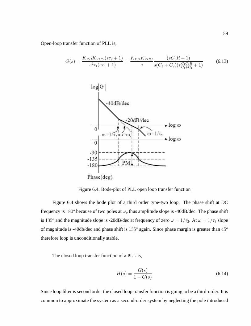
59
Open-loop transfer function of PLL is,
G(s) =KPDKV CO(sτ2 + 1)
s2τ1(sτ3 + 1)=
KPDKV CO
s
(sC1R + 1)
s(C1 + C2)(sC1C2RC1+C2
+ 1)(6.13)
Figure 6.4. Bode-plot of PLL open loop transfer function
Figure 6.4 shows the bode plot of a third order type-two loop.The phase shift at DC
frequency is180o because of two poles atωo thus amplitude slope is -40dB/dec. The phase shift
is 135o and the magnitude slope is -20dB/dec at frequency of zeroω = 1/τ2. At ω = 1/τ3 slope
of magnitude is -40db/dec and phase shift is135o again. Since phase margin is greater than45o
therefore loop is unconditionally stable.
The closed loop transfer function of a PLL is,
H(s) =G(s)
1 + G(s)(6.14)
Since loop filter is second order the closed loop transfer function is going to be a third-order. It is
common to approximate the system as a second-order system byneglecting the pole introduced

60
by C2 which is approximately 20 times greater than crossover frequency [21]. The closed loop
transfer function represented in control system approach is,
H(s) =2ζωns + ω2
n
s2 + 2ζωns + ω2n
(6.15)
Natural frequency of the system (ωn) is defined by,
ωn =
√
KPDKV CO
NC1
(6.16)
Crossover frequency is defined by,
ωc = 2ζωn (6.17)
Damping factor (ζ) is defined by,
ζ =1
2
√
KPDKV COR2C1
N(6.18)
The frequency of zero (ωz) is defined by,
ωz =ωn
2ζ=
1
RC1(6.19)
The frequency of third pole (ω3rd) is,
ω3rd =C1 + C2
C1C2R=
21
RC1(6.20)
The 3dB frequency of a second order closed loop system is defined by,
ω3dB = ωn
√
2ζ2 + 1 +√
(2ζ2 + 1)2 + 1 (6.21)

61
In more simple form, crossover frequency is very close to 3dBfrequency and they both can be
written as,
ωc = ω3dB = 2ζωn (6.22)
However this is valid for damping factors greater than 2. Figure 6.5 shows the plot of both (6.21)
and (6.22) and represents the ratio ofω3dB/ωn.
Figure 6.5. Output of two functions for 3dB frequency ratio
For higher values ofζ both equations are valid to determineω3dB andωc. For small values
of ζ and which is the case for this design (6.21) gives better approximation forω3dB.
Adjusting PLL parameters comes with trade-off between faster switching and lower ref-
erence spurs. Increasing the loop bandwidth decreases locktime however increasing reference
spur levels In opposite way decreasing the loop bandwidth increases the lock time but helps
reducing reference spur levels [22].
Based on the parameters of loop components calculated in previous sections the loop filter
design is straightforward. Loop bandwidth with unity damping (ζ = 1) for typical process

62
parameters is chosen to be,
fn = 550kHz (6.23)
yielding a crossover frequency of,
fc = 2ζfn = 1.1MHz (6.24)
At desired bandwidth (fn = 550kHz) the corresponding capacitance value forC1 is found to be
C1 = 293pF (6.25)
Figure 6.6 shows the plot of natural frequency versus loop filter capacitance (C1).
Figure 6.6. Natural frequency versus loop filter capacitance (C1)
SinceC2 is assumed to be 20 times less thanC1,
C2 = 14.7pF (6.26)

63
The resistance for unity damping (ζ = 1) is calculated with (6.18) is found to be,
R = 2kΩ (6.27)
A MATLAB script written as a single m-file is given in Appendix-B to calculate loop filter
components and determine bode plot of open loop transfer function and closed loop response. In
Figure 6.7 bode plot of open loop transfer function is shown.Phase margin is found to be65.1o
which satisfies the condition for stable loop at crossover frequency 1.06 MHz. In Figure 6.8
amplitude plot of closed loop system is shown. Peaking at 450kHz is observed due to zero
introduced by the loop filter resistor. The 3dB frequency of the closed loop system is found to
be 1.54 MHz.
Figure 6.7. Open-Loop AC response of PLL
6.2.1. Loop Filter Implementation with MOSFET Capacitance
Loop filter components are on-chip devices therefore they are implemented within the
integrated circuit. Loop filter capacitors are implementedwith NMOS capacitance and resistor

64
Figure 6.8. Closed-loop AC response of PLL
is implemented with HRI High Resistivity Poly resistor. Theschematic of loop filter with HRI
resistor and NMOS capacitance is shown in Figure 6.9.
Figure 6.9. Loop filter implementation with NMOS capacitance
NMOS capacitor is highly linear if it is biased above threshold. Its value varies negligi-
bly with temperature and process. Thus an NMOS capacitor is used to implement loop filter
capacitor. Figure 6.10 shows charging of an ideal capacitorand MOS capacitor biased above
threshold.
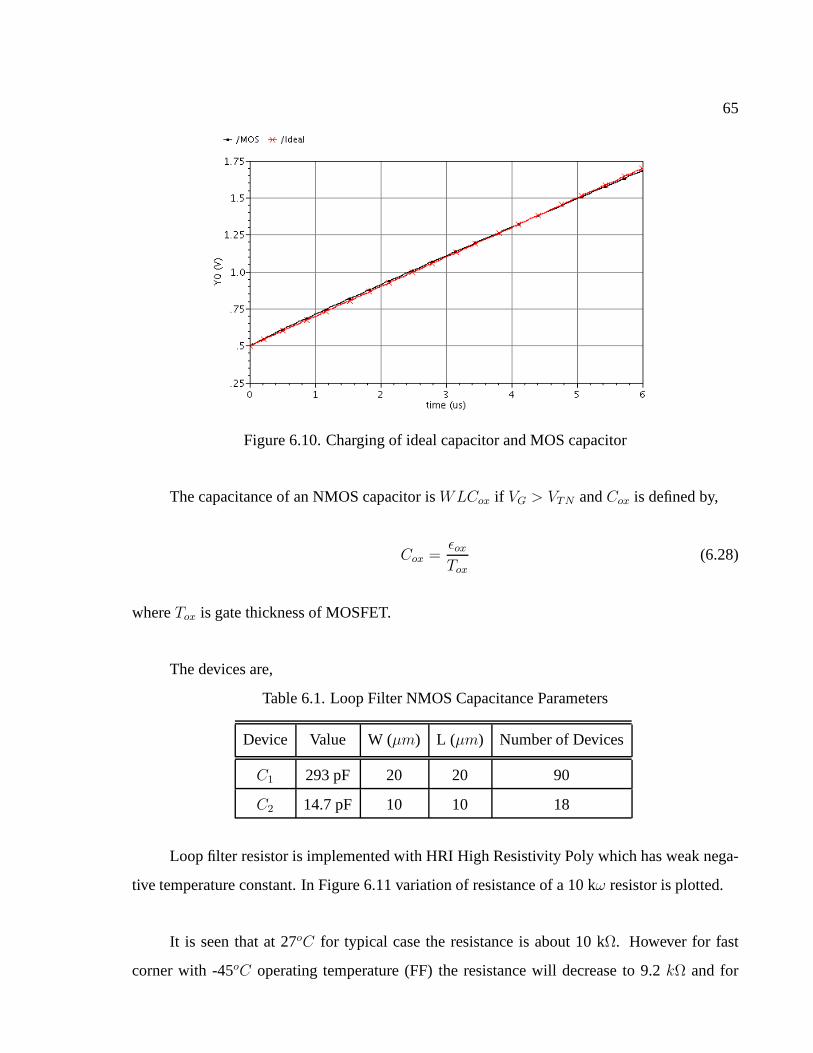
65
Figure 6.10. Charging of ideal capacitor and MOS capacitor
The capacitance of an NMOS capacitor isWLCox if VG > VTN andCox is defined by,
Cox =εox
Tox(6.28)
whereTox is gate thickness of MOSFET.
The devices are,
Table 6.1. Loop Filter NMOS Capacitance Parameters
Device Value W (µm) L (µm) Number of Devices
C1 293 pF 20 20 90
C2 14.7 pF 10 10 18
Loop filter resistor is implemented with HRI High Resistivity Poly which has weak nega-
tive temperature constant. In Figure 6.11 variation of resistance of a 10 kω resistor is plotted.
It is seen that at 27oC for typical case the resistance is about 10 kΩ. However for fast
corner with -45oC operating temperature (FF) the resistance will decrease to9.2 kΩ and for

66
Figure 6.11. Resistance variation versus temperature and process
slow corner with 125oC operating temperature it increases to 10.5kΩ with a relative change of
10 per cent. Also it is worth to mention that NMOS capacitancevaries very less with temperature
therefore affecting loop dynamics negligibly.
Since resistance varies with temperature and process, it iscrucial to analyze damping
coefficient and therefore stability of loop the loop. For fast corner operation (T=-45oC, ICP =
11µA andKV CO = 10GHz/V ), natural frequencyfn of the loop increases slightly and becomes
0.69 MHz. The loop filter resistance (R) decreases to 1.8 kΩ and resulting damping factorζ is
equal to 1.14.
For slow corner operation (T=125oC, ICP = 9.48µA andKV CO = 3.8GHz/V ), natural
frequencyfn decreases to 0.39 MHz. Loop filter resistance R increases to 2.2 kω and resulting
damping factorζ = 0.8. For both corner operation (FF and SS) damping factorζ ≥ 0.707 and
stability is ensured.

67
7. TOP LEVEL PLL SIMULATION
7.1. Transient Simulation
The stability of analysis of PLL is based on s-domain representation of each building
block. After determining the bandwidth and loop filter parameters transient simulation of PLL
in transistor level is done. Figure 7.1 plots the simulationof PLL from 0V VCO control voltage.
(a) Frequency (b) VCO control voltage
(c) Total current
Figure 7.1. PLL top-level Simulation - Kickstart
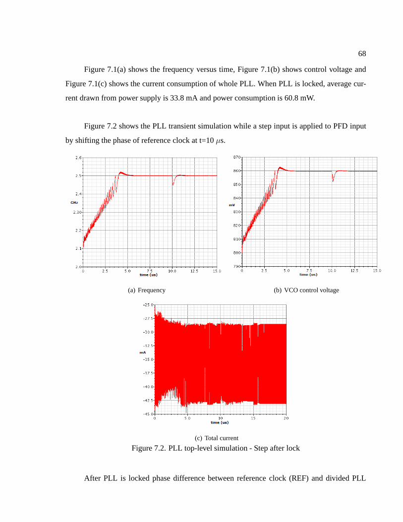
68
Figure 7.1(a) shows the frequency versus time, Figure 7.1(b) shows control voltage and
Figure 7.1(c) shows the current consumption of whole PLL. When PLL is locked, average cur-
rent drawn from power supply is 33.8 mA and power consumptionis 60.8 mW.
Figure 7.2 shows the PLL transient simulation while a step input is applied to PFD input
by shifting the phase of reference clock at t=10µs.
(a) Frequency (b) VCO control voltage
(c) Total current
Figure 7.2. PLL top-level simulation - Step after lock
After PLL is locked phase difference between reference clock (REF) and divided PLL

69
clock is expected to be zero. However due to gate leakage currentIleak of MOSFET capacitances
and possible mismatch errors in charge-pump results in verysmall phase offset between two
inputs of PFD. Phase-offset for single reference clock period is defined by,
∆φ =2πIleak
ICP
(7.1)
showing that increasing charge pump current decreases phase offset. Measured phase offset for
input is 44 pS and for 8 nS reference clock period this difference yields1.98o phase offset.
7.2. Phase Noise Analysis of PLL
Simulating PLL takes very long time because period of VCO is very small compared to
lock time of PLL. This is true when PLL is simulated in terms ofvoltages and currents. However
it is possible formulate models based on the phase of the signals namely phase-domain model
[23]. The phase-domain of a PLL is represented in Figure 7.3.Here, noise contribution of each
block of PLL is injected to the loop after each block.
Figure 7.3. Phase domain model of PLL
The most dominant phase noise source in PLL is VCO. For this analysis the noise con-
tribution of VCO is analyzed and the rest of noise sources areneglected. The transfer function
between output and input of PLL is already defined as,
φo(s)
φi(s)= H(s) =
NKPDKV COF (s)
Ns + KPDKV COF (s)(7.2)

70
where N is the feedback divider ratio. Writing the transfer function between output and VCO
yields,
φo(s)
φvco(s)=
Ns
Ns + KPDKV COF (s)= 1 − H(s) (7.3)
The loop filter is a low-pass filter and (7.2) states that noisefrom the PLL input is suppressed
by the loop filter. Equation (7.3) simply shows that the low frequency noise from the VCO
is filtered but high frequency noise components are passed tothe PLL output.In other words
increasing the loop BW reduces the effect of VCO jitter whiledecreasing it reduces input jitter.
Phase noise of VCO is injected to ideal model of PLL. Bandwidth parameters are already
calculated and phase noise of PLL output is obtained with those parameters. Resulting phase
noise plot of PLL is shown in Figure 7.4. Effect of PLL noise issuppressed in frequencies less
Figure 7.4. PLL Phase Noise
than loop bandwidth. After crossing the loop bandwidth the phase noise of VCO is fully seen
at the output of PLL due to high pass characteristic ofφo(s)/φV CO(s). Phase noise at 100 kHz
offset is -93 dB and at 600 kHz offset -87 dB. Phase noise of VCOdecreases with frequency

71
however output phase noise of PLL increases due to peaking introduced by the zero in the loop
filter. This shows how loop bandwidth affects output phase noise of PLL.
The relationship between phase noise and jitter can be calculated by integrating the power
spectral density of PLL output phase noise [24]. The variance for absolute jitter is related to the
total area of it the output PSD spectrum and it is defined by,
σ2A =
1
(2πfo)2
∫
∞
0
Sφ(f) df. (7.4)
whereSphi(f) is the spectral density of phase noise in units ofrad2/Hz.
Using 7.4 absolute jitter is found to be,
σA = 5.6pSRMS (7.5)
and peak-to-peak jitter is found to be,
6σA = 36.6pSpeak − to − peak (7.6)
Jitter quantity based on PSD of phase noise output of PLL is calculated. For more accurate
results phase noise contribution of other blocks of PLL should also be taken into consideration.

72
8. CONCLUSION
This work has presented the analysis and design of a high-frequency low-jitter clock syn-
thesizing PLL at 2.5GHz. The design is a conventional charge-pump PLL utilizing a 3-stage
ring oscillator with Maneatis-type loaded delay cells. Thekey design issues demonstrated in
this work can be summarized as follows:
• Linearly modeling the 3rd order PLL - which is in fact a discrete-time system - for stability
and noise analysis in frequency domain
• Identifying the non-idealities in the loop control components (PFD, charge pump, and loop
filter) and reducing their effects on PLL output noise.
• Designing a low noise VCO immune to GND/VDD bounce
• Developing a methodology to estimate VCO jitter contribution at the PLL output via Spec-
treRF phase-noise simulation together with spectre’s noise analysis
• Checking the design over all process corners and a wide temperature range (-40oC to
125oC)
• Investigating the use of high speed CML gates to build very high speed dividers
The final design is simulated to successfully synthesize a 2.5 GHz clock from a 125 MHz
clock source over all PVT (process, voltage, temperature variation). The absolute jitter contri-
bution of the VCO (main jitter source in the loop as long as other loop components are properly
designed) at the PLL output is estimated to be 5.6ps RMS. The PLL’s average power dissipation
is 60.8 mW (1.8V power supply). The PLL performance parameters are summarized in Table
8.1.

73
Table 8.1. PLL Summary
Parameter Value
Output Frequency 2.5 GHz
Reference Frequency 125 MHz
Divider Ratio (N) 20
Power Dissipation 60.8 mW
Absolute Jitter 5.6 pS (RMS), 36.6 pS (peak-to-peak)

74
APPENDIX A: Logical Effort
The method of logical effort is a way to estimate delay in a CMOS circuit. Delay estimates
of different logic structures can be compared and fastest one is selected. Also ideal number of
logic stages and proper transistor sizes for logic gates on apath is determined. Because it is an
easy method evaluating different alternatives provides a good starting point at early stages of a
design [25].
A.1. Delay in a Logic Gate
The method of logical effort is based on simple model of the delay through a single MOS
logic gate. The delay is caused by capacitive load which the logic gate drives and the topology
of the logic gate. Simply, as the load increases the delay increases. Also the delay depends on
logic function of the gate.
Inverters are the simplest logic gates that drive capacitive loads. They are also used to
drive large capacitve loads. However a different gate like NAND which computes a different
function requires more transistors some of which connectedin series. Therefore a longer delay
is expected from a NAND gate when compared to an inverter.
Based on delay of an inverter a unit delayd can be expressed as:
d = f + p (A.1)
p is a fixed delay calledparasitic delayandf is proportional to the load at the gate’s output
calledeffort delayor stage effort. The effort delay depends on two elements.Logical effortg is
related with gate’s properties andelectrical effortis related with load. In terms of these elements

75
effort delay can be expressed as,
f = gh (A.2)
Logical effortg depends on the logic gate’s topology and it’s ability to produce output current.
Electrical efforth describes how the electrical environment of the logic gate and size of the
transistors of the logic gate determine gate’s load drivingcapability. Electrical effort is expressed
as:
h =Cout
Cin
(A.3)
Cout is the capacitance that loads the gate’s output andCin is the capacitance of the gate’s input
terminal. Electrical effort is also called asfanout. Combining A.1 and A.2 yields,
d = gh + p (A.4)
The electrical effort,h, combines the effects of external load, which establishesCout, with the
sizes of the transistors in the logic gate, which establishCin. The logical effortg expresses the
effects of circuit topology on the delay independent of loading or transistor size. Logical effort
is useful because it depends only on circuit topology. Logical effort values for a few CMOS
logic gates are shown in Figure A.1(a)
(a) logical effort of gates (b) parasitic delay of gates
Figure A.1. Delay Values of different logic gates

76
The parasitic delayp expresses the intrinsic delay of the gate due to its own internal capac-
itance which is mostly independent of size of transistors inlogic gate. A list of parasitic delay
of some basic gates are shown in Figure A.1(b).
Based on the information on delays given above and considering delay Equation A.8
amount of delay of an inverter and 2-Input NAND gate can be calculated. Shown in Figure A.2,
the delay of two gates are observed on a plot.
Figure A.2. Plots of delay equation for an inverter and two-input NAND gate
Example: Estimate the delay of a fanout-of-4 (FO4) inverter shown in Figure A.3.
Because each inverter is identicalCout = 4Cin soh = 4. According to Equation A.8 delay is
d = gh + p = 1x4 + pinv = 5. It is sometimes suitable to express delay in terms of FO4 delay
because of it is commonly known for each process.
A.2. Multistage Logic Networks
So far delay is expressed in terms of a single logic gate and its load at the output. If the
delay of a path which consists of multiple logic gates, delayparameters of the previous preceding

77
Figure A.3. An inverter driving four identical inverters
chapter is generalized in terms of a path delay.
UppercaseG denotespath logical effortso it is distinguished fromg. Subscripti indexes
the logic stages along the path.
G =∏
gi (A.5)
UppercaseH now indicates the electrical effort of along a path.
H =Cout
Cin
(A.6)
In that caseCout andCin refer to output and input capacitance of a path. At that pointa new kind
of effort, named Branching Effort is introduced to account for fanout within a network. When
fanout occurs within a logic network, some of the available drive current is directed along the
path we are analyzing, and some is directed off that path.We de?ne the branching effort b at the
output of a logic gate to be
b =Con−path + Coff−path
Con−path=
Ctotal
Cuseful(A.7)
whereCon−path is the load capacitance along the path we are analyzing andCoff−path is the
capacitance of connections that lead off the path. Note thatif the path does not branch, the
branching effort is one. The branching effort along an entire path B is the product of the branch-

78
ing effort at each of the stages along the path.
G =∏
bi (A.8)
with definitions of logical, electrical, and branching effort along apath, we can define the path
effort F. Again, we use an uppercase symbol to distinguish the path effort from the stage effort f
associated with a single logic stage. The equation that defines path effort is,
F = GBH (A.9)
Note that the path branching and electrical efforts are related to the electrical effort of each stage:
BH =Cout
Cin
G =∏
bi = G =∏
hi (A.10)
The path delay D is the sum of the delays of each stages of logicin the path. Path delay D
is defined by,
D =∑
di = DF + P (A.11)
where path effort delayDF is,
D =∑
gihi (A.12)
and the path parasitic delay,
p =∑
pi (A.13)
The path is least when each stage in the path occupies same stage effort. The minimum delay is

79
achieved when stage effort is,
f = gihi = F 1/N (A.14)
Therefore minimum achievable delay in a path is defined by,
D = NF 1/N + P (A.15)
Then each logic stage should be designed with electrical effort,
hi =F 1/N
gi(A.16)
From this relationship, we can determine the transistor sizes of gates along a path. Start at the
end of the path and work backward, applying the capacitance transformation,
C(in)i =g(out)i
f(A.17)
This determines the input capacitance of each gate, which can then be distributed appropriately
among the transistors connected to the input. This process is exemplified with the following
example.
Example: Size the circuit in Figure A.4 for minimum delay. Suppose theload is 20
microns of gate capacitance and that the inverter has 10 microns of gate capacitance.
Figure A.4. Multistage path with different gates

80
Assuming minimum-length transistors, gate capacitance isproportional to gatewidth. Hence,
it is convenient to express capacitance in terms of microns of gate width, as given in this prob-
lem.The path has logical effort G = 1 x (5/3) x (4/3) x 1 = 20/9. The electrical effort is H = 20/10
= 2, and the branching effort is 1. Thus, F = GBH = 40/9, andf = (40/9)1/4= 1.45.
Start from the output and work backward to compute sizes: z = 20 x 1/1.45 = 14, y = 14
x (4/3)/1.45 = 13, and x = 13 x (5/3)/1.45 = 15. These input gatewidths are divided among the
transistors in each gate. Notice that the inverters are assigned larger electrical efforts than the
more complex gates because they are better at driving loads.

81
APPENDIX B: MATLAB Loop Filter Design Script
%% pll_sim.m
function pll_sim
s = tf(’s’);
%% User Inputs - 1
display(’Enter Circuit Metrics: ’);
display(’ ’);
Kvco = input(’VCO Gain (GHz/V): ’);
Kvco = Kvco * 2* pi * 10ˆ9;
Icp = input(’Charge Pump Current (uA): ’);
Icp = Icp/(2 * pi) * 10ˆ-6;
N = input(’Feedback Divider Counter Value (N): ’);
%% User Inputs - 2
display(’ ’);
display(’Enter PLL Loop Filter Metrics: ’);
display(’ ’);
fn = input(’Loop Bandwith (MHz): ’);
fn= fn * 10ˆ6;
zeta = input(’Damping Coefficient: ’);
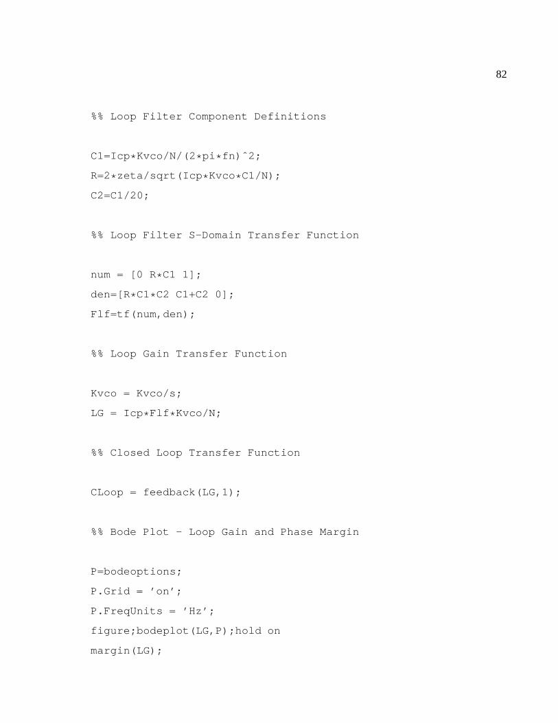
82
%% Loop Filter Component Definitions
C1=Icp * Kvco/N/(2 * pi * fn)ˆ2;
R=2* zeta/sqrt(Icp * Kvco * C1/N);
C2=C1/20;
%% Loop Filter S-Domain Transfer Function
num = [0 R* C1 1];
den=[R * C1* C2 C1+C2 0];
Flf=tf(num,den);
%% Loop Gain Transfer Function
Kvco = Kvco/s;
LG = Icp * Flf * Kvco/N;
%% Closed Loop Transfer Function
CLoop = feedback(LG,1);
%% Bode Plot - Loop Gain and Phase Margin
P=bodeoptions;
P.Grid = ’on’;
P.FreqUnits = ’Hz’;
figure;bodeplot(LG,P);hold on
margin(LG);

83
%% Closed Loop Simulation
P=bodeoptions;
P.Grid = ’on’;
P.FreqUnits = ’Hz’;
figure;bodeplot(CLoop,P);hold on
title(’Closed-Loop Bode Diagram’);
%% Step Response of the System
figure;pzmap(CLoop);
title(’Step Response of the System’);
%% Display Capactior and Resistor Values
display(’ ’);
display(’ ’);
display(’--------------------------------’);
disp([’Clarge=’ num2str(C1)]);
display(’ ’);
disp([’Csmall=’ num2str(C2)]);
display(’ ’);
disp([’R=’ num2str(R)]);
display(’--------------------------------’);

84
REFERENCES
1. Razavi, B.,Monolithic Phase Locked Loops and Clock Recovery Circuits, IEEE Press, 1996.
2. Kaenel, V., D. Aebicher, C. Piguet and E. Dijkstra, “A 320 MHz 1.5mW at 1.35 V CMOS
PLL for Microprocessor Clock Generation”, Journal of Solid-State Circuits, November
1996.
3. Terlemez, B.,Oscillation Control in CMOS Phase-Locked Loops, Ph.D. thesis, Georgia
Institute of Technology, 2004.
4. Gray, P., P. Hurst, R. Meyer and S. Lewis,Analysis and Design of Analog Integrated Cir-
cuits, John Wiley & Sons, 4th edn., 2001.
5. Fischette, D., “Practical Phase-Locked Loop Design”, ISSCC, 2004.
6. Hastings, A.,The Art of Analog Layout, Prentice Hall, 2nd edn., 2006.
7. Razavi, B.,Design of Analog CMOS Integrated Circuits, McGraw Hill, 4th edn., 2001.
8. Young, I. A., J. K. Greason and K. L. Wong, “A PLL Clock Generator with 5 to 110 MHz
of Lock Range for Microprocessors”, IEEE Journal of Solid-State Circuits, Vol. 27, No. 11,
November 1992.
9. Hsieh, M. T. and G. E. Sobelman, “Comparison of LC and Ring VCOs for PLLs in a 90 nm
Digital CMOS Process”, Proceedings of International SoC Design Conference, pp. 19–22,
2006.
10. Razavi, B.,RF Microelectronics, Prentice Hall, 1998.
11. Pak, B.,2.4 GHz CMOS PLL Frequency Synthesizer, Master’s thesis, Istanbul Teknik Uni-

85
versitesi, May 2002.
12. Dai, L. and R. Harjani, “Design of Low-Phase-Noise CMOS Ring Oscillators”, IEEE Trans-
actions on Circuits and Systems, Vol. 49, No. 5, May 2002.
13. Lee, T. H.,The Design of CMOS Radio-Frequency Integrated Circuits, Cambridge Univer-
sity Press, 1998.
14. Baker, J.,CMOS: Circuit Design, Layout and Simulation, Wiley-IEEE, 2nd edn., 2008.
15. Maneatis, J. G. and M. A. Horowitz, “Precise Delay Generation Using Coupled Oscilla-
tors”, IEEE Journal of Solid-State Circuits, Vol. 28, No. 12, December 1993.
16. Maneatis, J. G., “Low-Jitter Process-Independent DLL and PLL Based on Self-Biased Tech-
niques”, IEEE Journal of Solid-State Circuits, Vol. 31, No. 11, November 1996.
17. Yuan, J. and C. Svensson, “High-Speed CMOS Circuit Technique”, IEEE Journal of Solid-
State Circuits, Vol. 24, No. 1, February 1989.
18. Vaucher, S. C., I. Ferencic, M. Locher, S. Sedvallson, U.Voegeli and Z. Wang, “A Family of
Low-Power Truly Modular Programmable Dividers in Standard0.35-µm CMOS Technol-
ogy”, IEEE Journal of Solid-State Circuits, Vol. 35, No. 7, July 2000.
19. Heydari, P., “A Family of Low-Power Truly Modular Programmable Dividers in Standard
0.35-µm CMOS Technology”, IEEE Transactions on Very Large Scale Integration (VLSI)
Systems, Vol. 12, No. 10, October 2004.
20. Nonis, R., E. Palumbo, P. Palestri and L. Selmi, “A Family of Low-Power Truly Modular
Programmable Dividers in Standard 0.35-µm CMOS Technology”, IEEE Transactions on
Circuits and Systems, Vol. 54, No. 2, February 2007.
21. Mirabbasi, S. and K. Martin, “Design of Loop Filter in Phase-Locked Loops”, Electronic
86
Letters, Vol. 35, No. 21, October 1999.
22. Banerjee, D.,PLL Performance, Simulation, and Design, 4th edn., 2006.
23. Kundert, K., “Predicting the Phase Noise and Jitter of PLL-Based Frequency Synthesizers”,
Designer’s Guide Consulting, Inc., August 2006.
24. Lee, D. C., “Analysis of Jitter in Phase-Locked Loops”, IEEE Transactions on Circuits and
Systems, Vol. 49, No. 11, November 2002.
25. Sutherland, I., B. Sproull and D. Harris,Logical Effort: Designing Fast CMOS Circuits,
Morgan Kaufmann Publishers Inc., San Francisco, CA, USA, 1999.