modeling and simulation of jitter in phase-locked …...modeling and simulation of jitter in...
TRANSCRIPT

Modeling and Simulation of Jitter in Phase-Locked Loops due to
Substrate Noise
Jae Wook Kim, Yi-Chang Lu and Robert W. DuttonStanford University
September 22, 2005
Outline
Introduction
Substrate Noise Coupling Mechanism and Modeling Technique
Comparison between Simulation Methodologies
Period Histogram and Comparison with Measurements
Conclusion
Outline
Introduction
Substrate Noise Coupling Mechanism and Modeling Technique
Comparison between Simulation Methodologies
Period Histogram and Comparison with Measurements
Conclusion
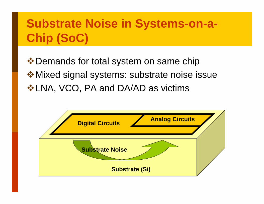
Substrate Noise in Systems-on-a-Chip (SoC)
Demands for total system on same chipMixed signal systems: substrate noise issueLNA, VCO, PA and DA/AD as victims
Substrate (Si)
Digital Circuits
Substrate Noise
Analog Circuits
Simulations for Analog Systems under Substrate Noise Environment
The simulations of substrate noise coupling to analog systems can be simple conceptually, but is definitely demanding in transistor-level and transient analysis mode.The blocks of an analog system are not equally sensitive to substrate noise. And substrate noise coupling mechanism itself is deterministic, thus allowing to abstract behavioral models.Considering these factors, simulations for PLL under substrate noise environment can be a challenging but good candidate.
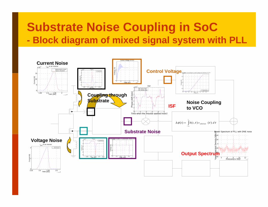
Substrate Noise Coupling in SoC- Block diagram of mixed signal system with PLL
Current Noise
Noise Couplingto VCO
1.85 1.9 1.95 2x 10⁻⁸
0
5
10
15
x 10-5
TIME [sec]
Cur
rent
[A]
Ivdd of an inverter
Mathematical modelHspice simulation
3.35 3.4 3.45 3.5x 10⁻⁸
0
1
2
TIME [sec]
Cur
rent
[A]
Ignd of an inverterMathematical modelHspice simulation
1.85 1.9 1.95 2 2.05x 10⁻⁸
-1
0
1
2
3
4
5x 10⁻³
TIME [sec]
Vol
tage
[V]
VdpbulkHspice simulationMathematical model
3.35 3.4 3.45 3.5 3.55x 10⁻⁸
-8
-6
-4
-2
0
2x 10⁻³
TIME [sec]
Volta
ge [V
]
VdnbulkHspice simulationMathematical model
0 0.5 1 1.5 2 2.5x 10
-5
0.6
0.7
TIME [sec]
Vol
tage
[V]
Control Voltage of VCO
4 6 8 10 12x 107
-60
-40
-20
0
20
40
Frequency [Hz]Pow
er S
pect
ral D
ensi
ty [d
Bc/
HPower Spectrum of PLL with DNE noise
0 0.2 0.4 0.6 0.8 1x 10⁻⁷
-10
-5
0
5 x 10⁻³
TIME [sec]
Vol
tage
[V]
themetical model of substrate noise at an
0 0.2 0.4 0.6 0.8 1 1.2 1.4 1.60
0.5
1
1.5
2
2.5
3 x 10⁸
Voltage [V]
Freq
uenc
y [H
z]
Charcteristic curve between a control voltage and a frequency of VCO
Hspice simulationCurve-fitted polynomial
10 15 20 25 30 35-4
-3
-2
-1
0
1
2
3 x 10-12
Time when the impulse applied [nsec]
Pha
se s
hift
[sec
]
ISF15th rising edge15th falling edge
τττφ dvthtt
substrate )(),()( ∫∞−
=∆
Control Voltage
ISF
Output Spectrum
Substrate Noise
Voltage Noise
Coupling throughSubstrate
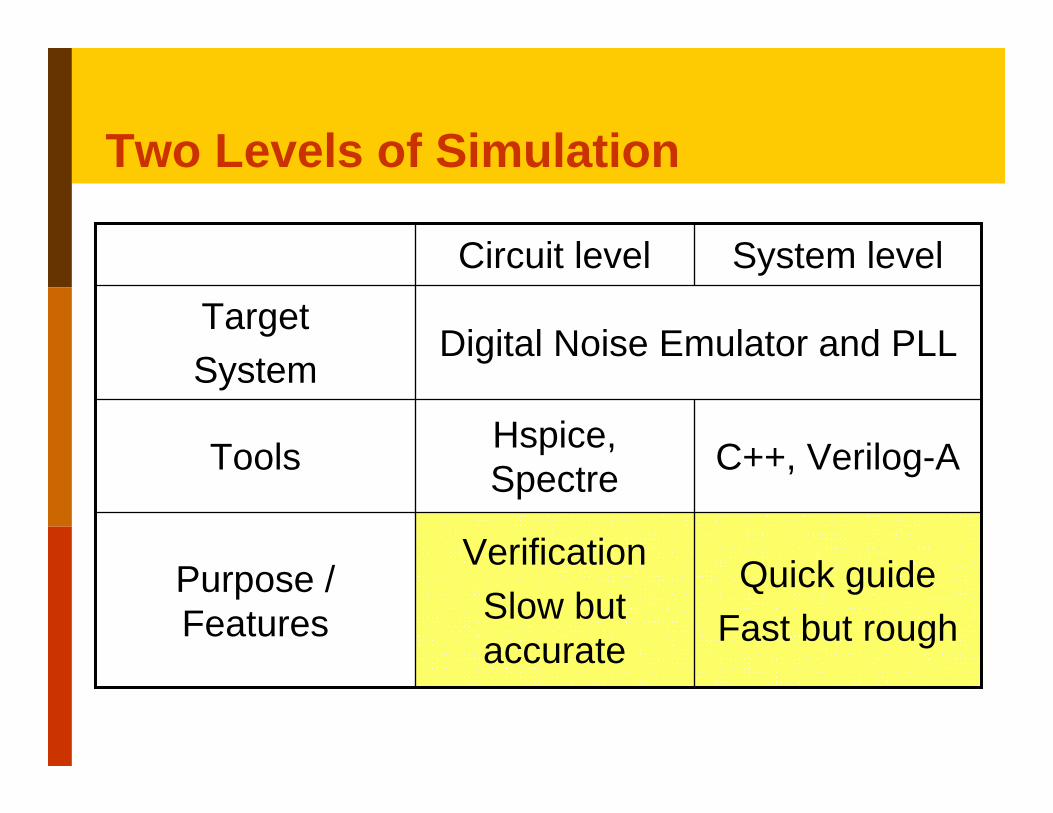
Two Levels of Simulation
Digital Noise Emulator and PLLTargetSystem
C++, Verilog-AHspice, SpectreTools
Quick guideFast but rough
VerificationSlow but accurate
Purpose / Features
System levelCircuit level
Outline
Introduction
Substrate Noise Coupling Mechanism and Modeling Technique
Comparison between Simulation Methodologies
Period Histogram and Comparison with Measurements
Conclusion

Substrate Noise Coupled to VCO
gnd
in out
bias
Vdd
nbulk
Converter
+
-
Inverter
1.4595 1.46 1.4605 1.461 1.4615 1.462 1.4625 1.463 1.4635 1.464
x 10-8
0
0.02
0.04
0.06
0.08
0.1
TIME [sec]
Nod
e V
olta
ge [V
]
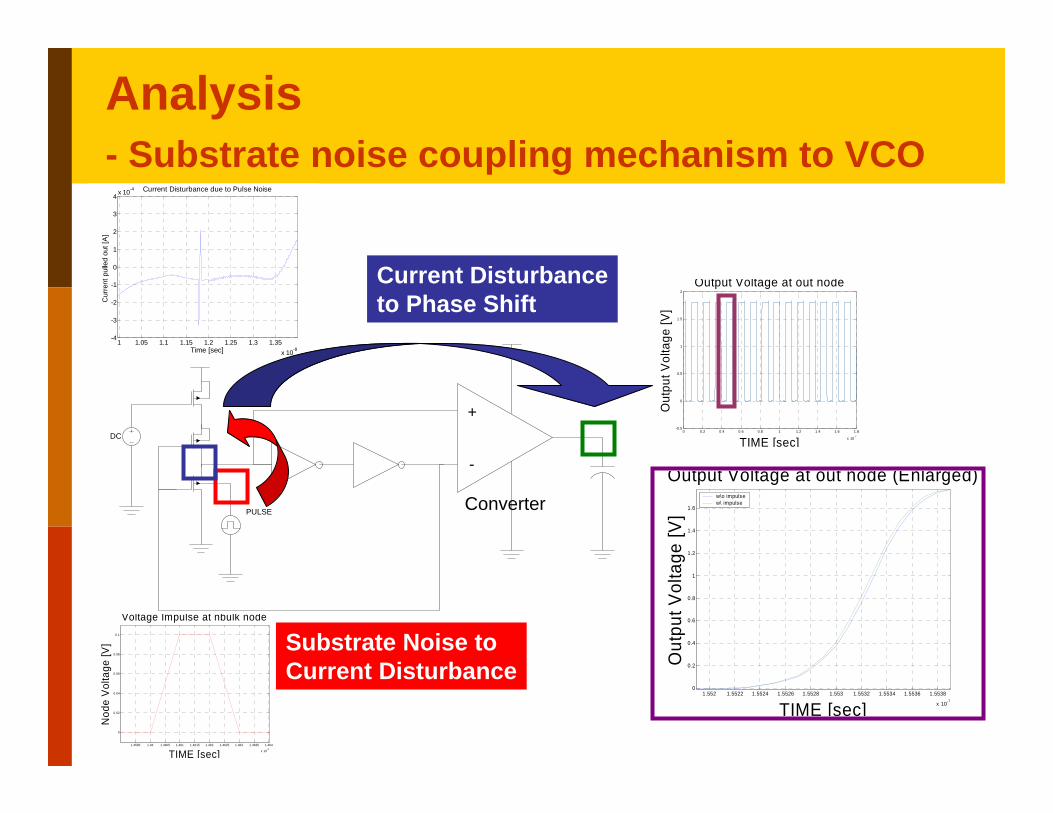
Voltage Impulse at nbulk node
0 0.2 0.4 0.6 0.8 1 1.2 1.4 1.6 1.8
x 10-7
-0.5
0
0.5
1
1.5
2
TIME [sec]
Out
put V
olta
ge [V
]
Output Voltage at out node
1.552 1.5522 1.5524 1.5526 1.5528 1.553 1.5532 1.5534 1.5536 1.5538
x 10-7
0
0.2
0.4
0.6
0.8
1
1.2
1.4
1.6
TIME [sec]
Out
put V
olta
ge [V
]
Output Voltage at out node (Enlarged)w\o impulsew\ impulse
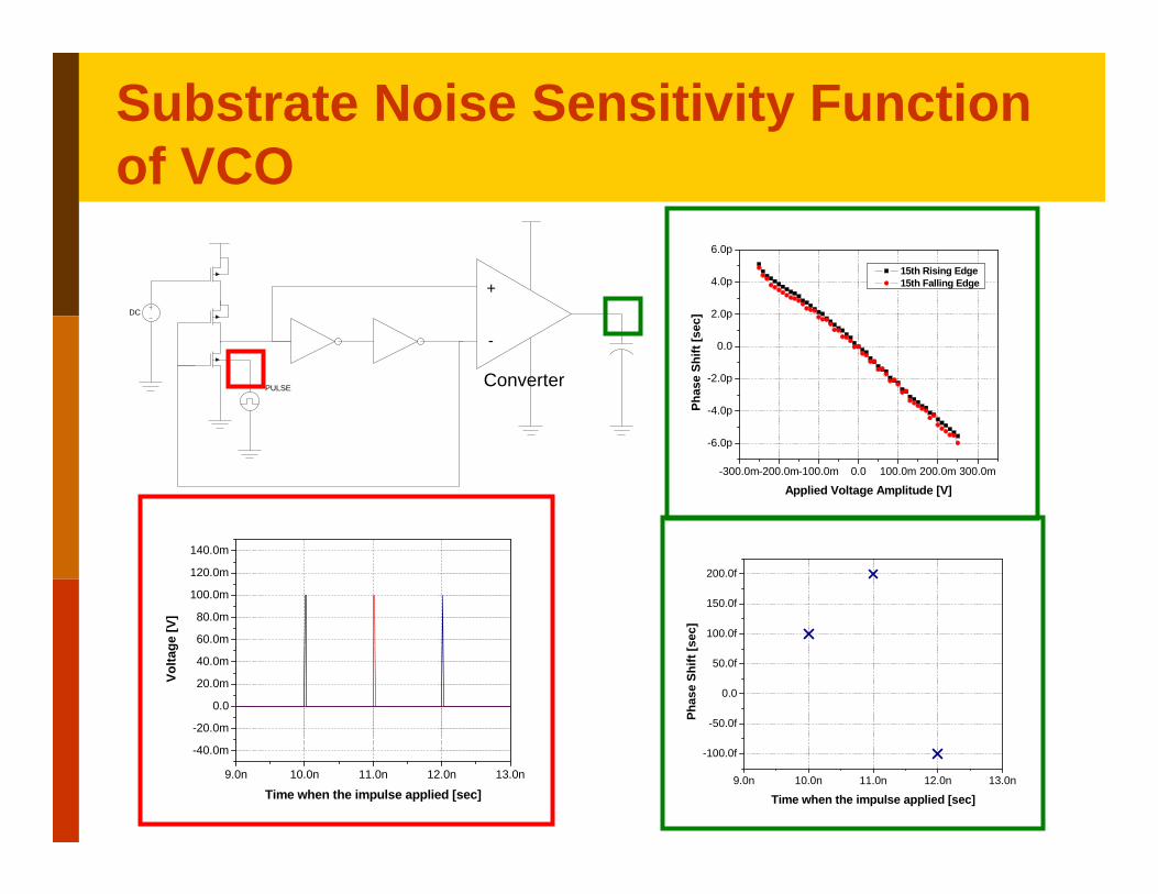
Substrate Noise Sensitivity Function of VCO
Converter
DC
PULSE
+
-
9.0n 10.0n 11.0n 12.0n 13.0n
-40.0m
-20.0m
0.0
20.0m
40.0m
60.0m
80.0m
100.0m
120.0m
140.0m
Volta
ge [V
]
Time when the impulse applied [sec]9.0n 10.0n 11.0n 12.0n 13.0n
-100.0f
-50.0f
0.0
50.0f
100.0f
150.0f
200.0f
Phas
e Sh
ift [s
ec]
Time when the impulse applied [sec]
-300.0m-200.0m-100.0m 0.0 100.0m 200.0m 300.0m
-6.0p
-4.0p
-2.0p
0.0
2.0p
4.0p
6.0p
Phas
e Sh
ift [s
ec]
Applied Voltage Amplitude [V]
15th Rising Edge 15th Falling Edge

Behavioral Model – Noise coupling equation
• ISFV – Impulse Sensitivity Function between substrate noise and phase shift
10.0n 15.0n 20.0n 25.0n 30.0n 35.0n
-2.5p
-2.0p
-1.5p
-1.0p
-500.0f
0.0
500.0f
Phas
e Sh
ift [s
ec]
Time when the impulse applied [sec]∫=t
dISFV∆Φ(t)0 vsub )()( τττ
Converter
DC
PULSE
+
-
1 1.05 1.1 1.15 1.2 1.25 1.3 1.35x 10⁻⁸
-4
-3
-2
-1
0
1
2
3
4 x 10⁻⁴
Time [sec]
Cur
rent
pul
led
out [
A]
Current Disturbance due to Pulse Noise
0 0.2 0.4 0.6 0.8 1 1.2 1.4 1.6 1.8
x 10-7
-0.5
0
0.5
1
1.5
2
TIME [sec]
Out
put V
olta
ge [V
]
Output Voltage at out node
1.4595 1.46 1.4605 1.461 1.4615 1.462 1.4625 1.463 1.4635 1.464
x 10-8
0
0.02
0.04
0.06
0.08
0.1
TIME [sec]
Nod
e V
olta
ge [V
]
Voltage Impulse at nbulk node
Analysis - Substrate noise coupling mechanism to VCO
Converter
DC
PULSE
+
-
Substrate Noise toCurrent Disturbance
Current Disturbanceto Phase Shift
1.552 1.5522 1.5524 1.5526 1.5528 1.553 1.5532 1.5534 1.5536 1.5538
x 10-7
0
0.2
0.4
0.6
0.8
1
1.2
1.4
1.6
TIME [sec]
Out
put V
olta
ge [V
]
Output Voltage at out node (Enlarged)w\o impulsew\ impulse
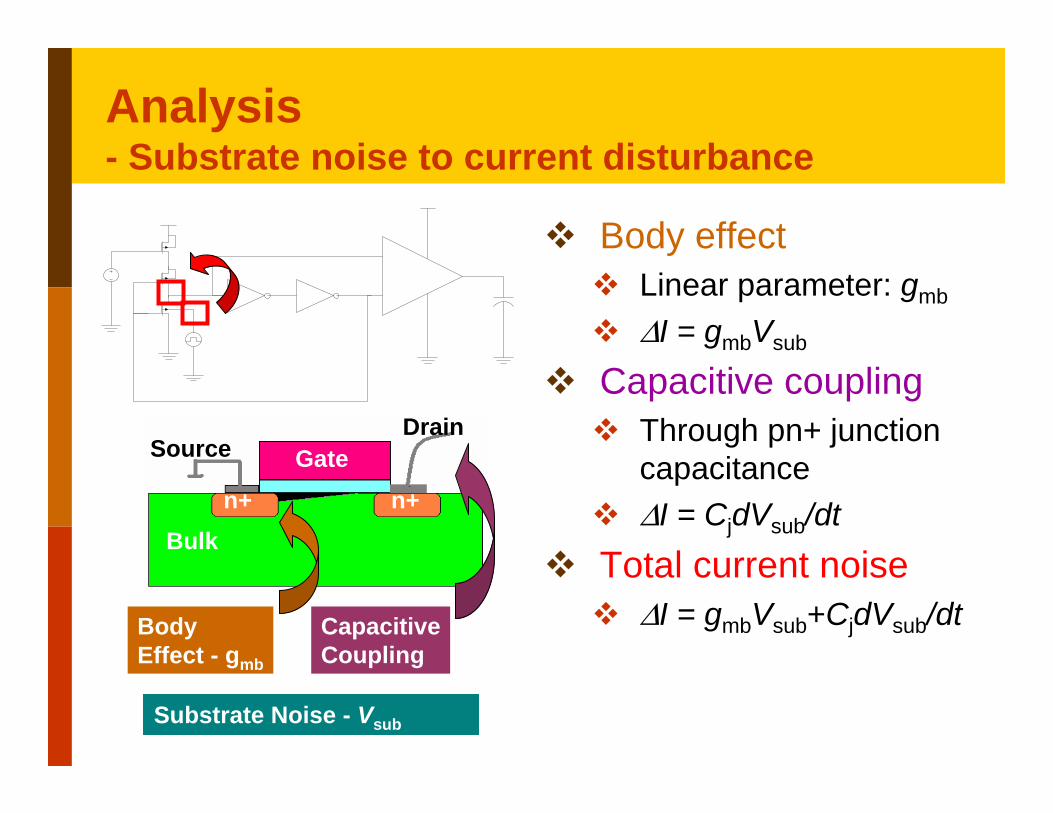
Analysis - Substrate noise to current disturbance
Body effectLinear parameter: gmb
∆I = gmbVsub
Capacitive couplingThrough pn+ junction capacitance∆I = CjdVsub/dt
Total current noise∆I = gmbVsub+CjdVsub/dt
Bulkn+ n+
SourceDrain
Gate
CapacitiveCoupling
BodyEffect - gmb
Substrate Noise - Vsub
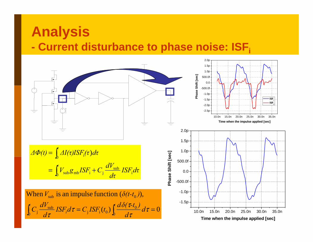
Analysis- Current disturbance to phase noise: ISFi
10.0n 15.0n 20.0n 25.0n 30.0n 35.0n
-1.5p
-1.0p
-500.0f
0.0
500.0f
1.0p
1.5p
2.0p
Phas
e Sh
ift [s
ec]
Time when the impulse applied [sec]
∫
∫+=
=
t
t
dτISFdτdVCISFgV
dτ(τISF∆I(τ)∆Φ(t)
0 isub
jimbsub
0 i )
0)(
),(function impulsean isWhen
00
0ij0sub
j
0sub
== ∫∫tt
i dd
)-tδ(dtISFCdISFddVC
)δ(t-tV
ττττ
τ
10.0n 15.0n 20.0n 25.0n 30.0n 35.0n
-2.5p
-2.0p
-1.5p
-1.0p
-500.0f
0.0
500.0f
1.0p
1.5p
2.0p
Phas
e Sh
ift [s
ec]
Time when the impulse applied [sec]
ISFi
ISFv

Behavioral Model – Noise coupling equation based on analysis
∫∫
∫∫
+=
+=+=
tt
tt
i
dτISFdτdVCdτISFV
dτISFdτdVCISFg(Vdτ)ISF
dτdVCg(V∆Φ(t)
0 isub
j0 vsub
0 isub
jimbsub0sub
jmbsub )
10.0n 15.0n 20.0n 25.0n 30.0n 35.0n
-2.5p
-2.0p
-1.5p
-1.0p
-500.0f
0.0
500.0f
Phas
e Sh
ift [s
ec]
Time when the impulse applied [sec]
ISFix gmb ISFv
imbv ISFgISF =
∫=t
dISFV∆Φ(t)0 vsub )()( τττ
∫=t
dτ(τISFgV∆Φ(t)0 imbsub )
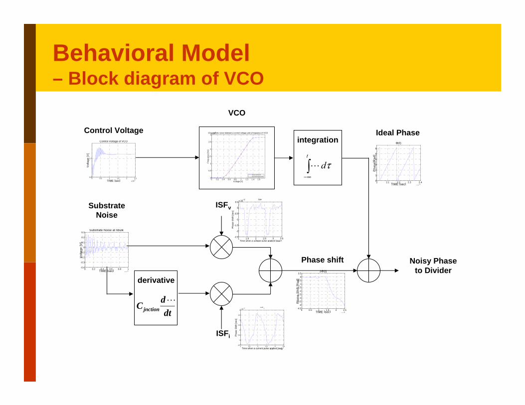
Behavioral Model – Block diagram of VCO
1 1.5 2 2.5 3 3.5x 10⁻⁸
-2.5
-2
-1.5
-1
-0.5
0
0.5x 10⁻¹²
Time when a voltage pulse applied [sec]
Phas
e S
hift
[sec
]
ISF
ISFv
integration
τdt
∫∞−
Noisy Phase to Divider
Substrate Noise
0 0.2 0.4 0.6 0.8 1x 10⁻⁷
-0.4
-0.3
-0.2
-0.1
0
0.1
0.2
0.3
TIME [sec]
Vol
tage
[V]
Substrate Noise at nbulk
VCO
0 0.2 0.4 0.6 0.8 1 1.2 1.4 1.60
0.5
1
1.5
2
2.5
3 x 10⁸
Voltage [V]
Freq
uenc
y [H
z]
Charcteristic curve between a control voltage and a frequency of VCO
Hspice simulationCurve-fitted polynomial
Ideal Phase
2 2.1 2.2 2.3 2.4x 10⁻⁷
0
1
2
3
4
5
6
TIME [sec]
Pha
se[R
ad]
Φ(t)
derivative
dtdCjnction
1 1.5 2 2.5 3 3.5x 10⁻⁸
-1.5
-1
-0.5
0
0.5
1
1.5
2x 10-12
Time when a current pulse applied [sec]
Phas
e S
hift
[sec
]
ISFi
ISFi
Phase shift
0 0.5 1 1.5 2 2.5x 10⁻⁵
-4.5-4
-3.5-3
-2.5-2
-1.5-1
-0.50
0.5
TIME [sec]
Pha
se S
hift
[Rad
]
∆Φ(t)
0 0.5 1 1.5 2 2.5x 10
-5
0.6
0.7
TIME [sec]
Vol
tage
[V]
Control Voltage of VCO
Control Voltage
Outline
Introduction
Substrate Noise Coupling Mechanism and Modeling Technique
Comparison between Simulation Methodologies
Period Histogram and Comparison with Measurements
Conclusion
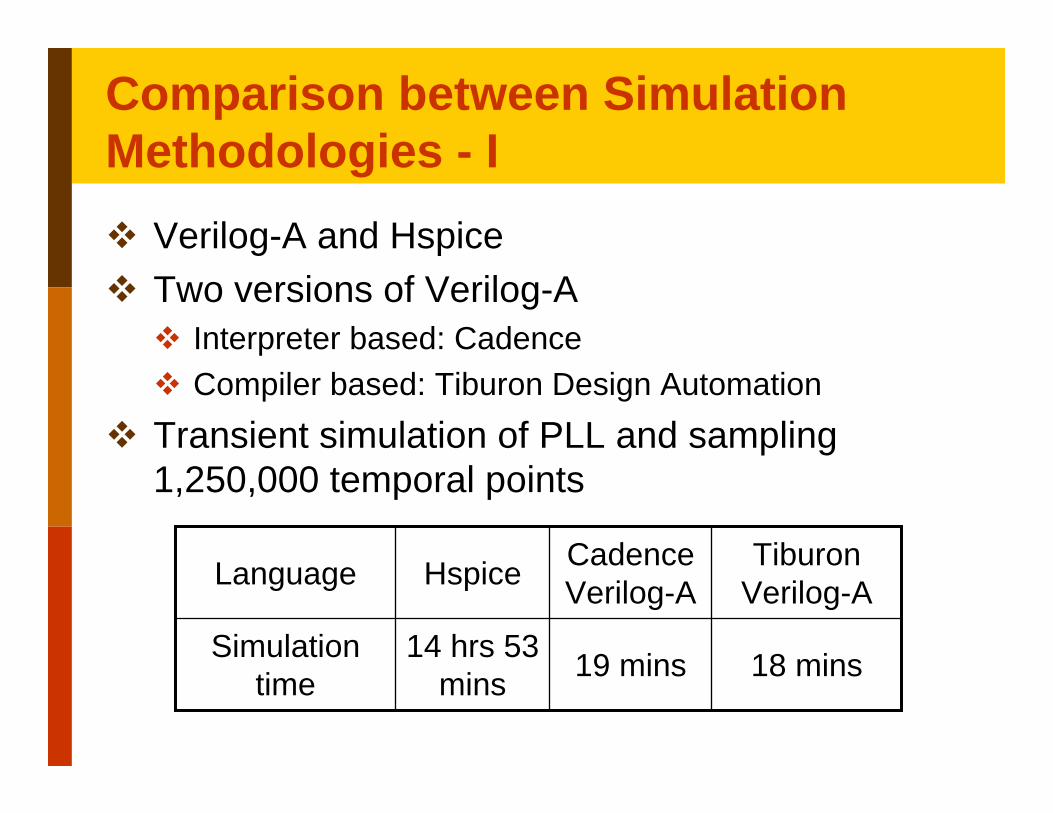
Comparison between Simulation Methodologies - I
Verilog-A and HspiceTwo versions of Verilog-A
Interpreter based: CadenceCompiler based: Tiburon Design Automation
Transient simulation of PLL and sampling 1,250,000 temporal points
18 mins19 mins14 hrs 53 mins
Simulation time
Tiburon Verilog-A
Cadence Verilog-AHspiceLanguage
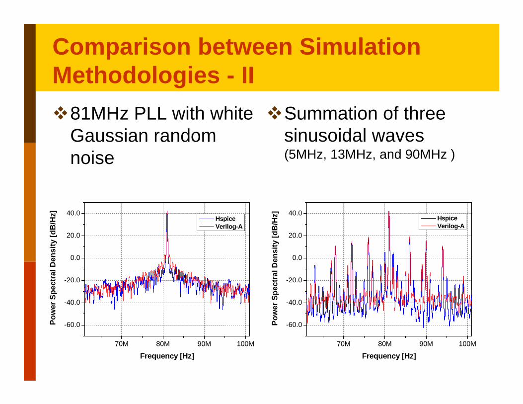
Comparison between Simulation Methodologies - II
81MHz PLL with white Gaussian random noise
Summation of three sinusoidal waves (5MHz, 13MHz, and 90MHz )
70M 80M 90M 100M
-60.0
-40.0
-20.0
0.0
20.0
40.0
Pow
er S
pect
ral D
ensi
ty [d
B/H
z]
Frequency [Hz]
Hspice Verilog-A
70M 80M 90M 100M
-60.0
-40.0
-20.0
0.0
20.0
40.0
Pow
er S
pect
ral D
ensi
ty [d
B/H
z]
Frequency [Hz]
Hspice Verilog-A

Outline
Introduction
Substrate Noise Coupling Mechanism and Modeling Technique
Comparison between Simulation Methodologies
Period Histogram and Comparison with Measurements
Conclusion
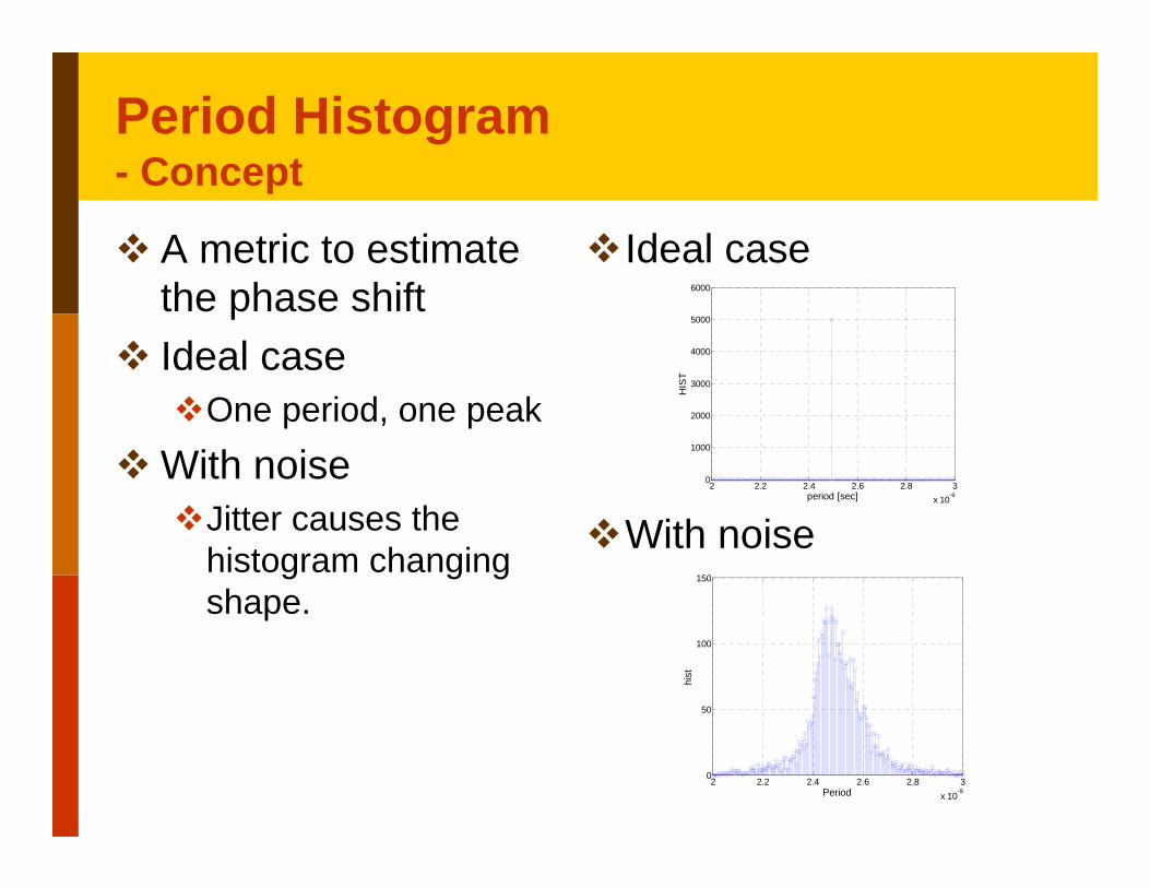
Period Histogram- Concept
A metric to estimate the phase shiftIdeal case
One period, one peak With noise
Jitter causes the histogram changing shape.
Ideal case
With noise2 2.2 2.4 2.6 2.8 3
x 10-9
0
1000
2000
3000
4000
5000
6000
period [sec]
HIS
T
2 2.2 2.4 2.6 2.8 3x 10⁻⁹
0
50
100
150
Period
hist

Period Histogram- Noise dependency
Periodic noise400MHz PLL with 100mV, 100MHz sinusoidal wave noisePeak splitting
Random noiseWith 100mV(RMS) white Gaussian noiseHistogram spreading
2.3 2.35 2.4 2.45 2.5 2.55 2.6 2.65 2.7x 10⁻⁹
0
50
100
150
Period
hist
2 2.2 2.4 2.6 2.8 3x 10⁻⁹
0
200
400
600
800
1000
1200
1400
period [sec]
HIS
T

0 0.2 0.4 0.6 0.8 1x 10⁻⁸
-4
-2
0
2x 10-12
0 0.2 0.4 0.6 0.8 1x 10⁻⁸
-0.1
0
0.1
0 0.2 0.4 0.6 0.8 1x 10⁻⁸
-1
0
1
x 10-10
ISF ( of three NMOS devices)
100MHz Sine Wave Noise
∆Φ = dtftISF
MHzofpeiord∫ ×
4001
)2sin(1.0 π
1/400MHz
Period Histogram- Variation with phase of noise
400MHz PLL with 100MHz sinusoidal noise
2 2.2 2.4 2.6 2.8 3x 10⁻⁹
0
200
400
600
800
1000
1200
1400
period [sec]
HIS
T0 0.2 0.4 0.6 0.8 1
x 10-8
-4
-2
0
2x 10-12
0 0.2 0.4 0.6 0.8 1x 10⁻⁸
-0.1
0
0.1
0 0.2 0.4 0.6 0.8 1x 10⁻⁸
-1
0
1
x 10-10
ISF ( of three NMOS devices)
100MHz Sine Wave Noise
∆Φ = dtftISF
MHzofpeiord∫ ×
4001
)2sin(1.0 π
1/400MHz
2 2.2 2.4 2.6 2.8 3x 10⁻⁹
0
500
1000
1500
2000
2500
period [sec]
HIS
T
2.4
2.45
2.5
2.55
2.6
x 10-9
0
50
100
150
200
250
300
350
020004000
Period [s]Phase [deg]
HIS
T
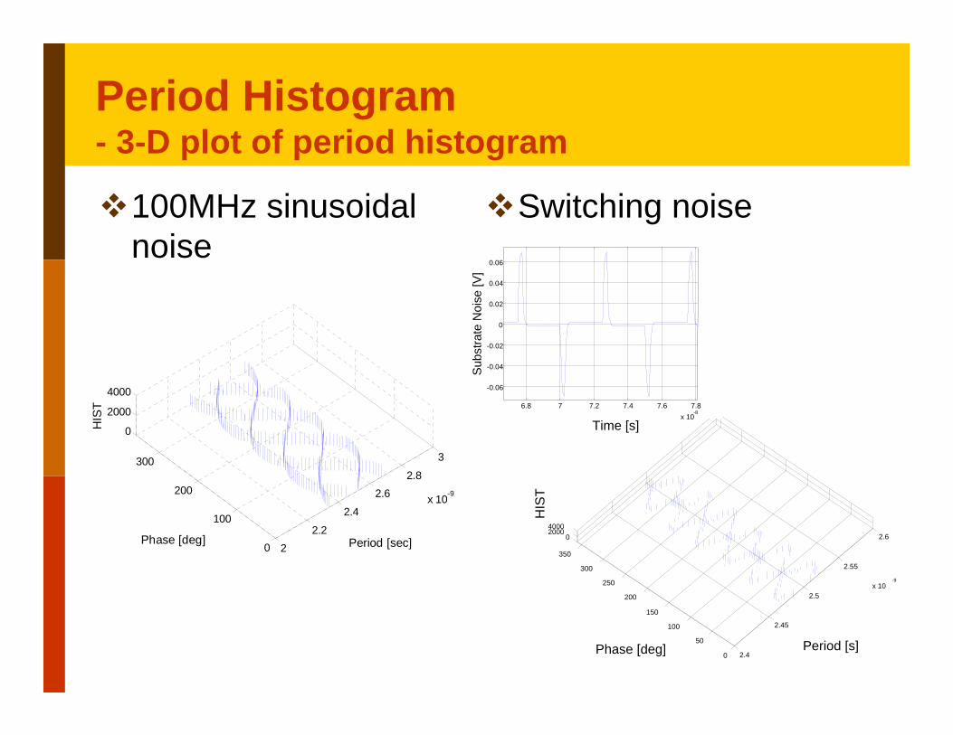
Period Histogram- 3-D plot of period histogram
Switching noise100MHz sinusoidal noise
22.2
2.4
2.62.8
3
x 10-9
0
100
200
300
0
2000
4000
Period [sec]Phase [deg]
HIS
T 6.8 7 7.2 7.4 7.6 7.8x 10
-8
-0.06
-0.04
-0.02
0
0.02
0.04
0.06
Time [s]
Subs
trate
Noi
se [V
]
5ns
bestworst
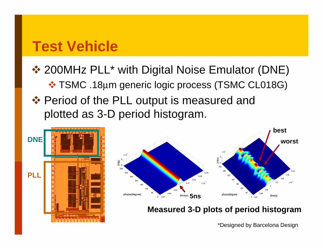
Test Vehicle200MHz PLL* with Digital Noise Emulator (DNE)
TSMC .18µm generic logic process (TSMC CL018G)Period of the PLL output is measured and plotted as 3-D period histogram.
*Designed by Barcelona Design
DNE
PLL
Measured 3-D plots of period histogram
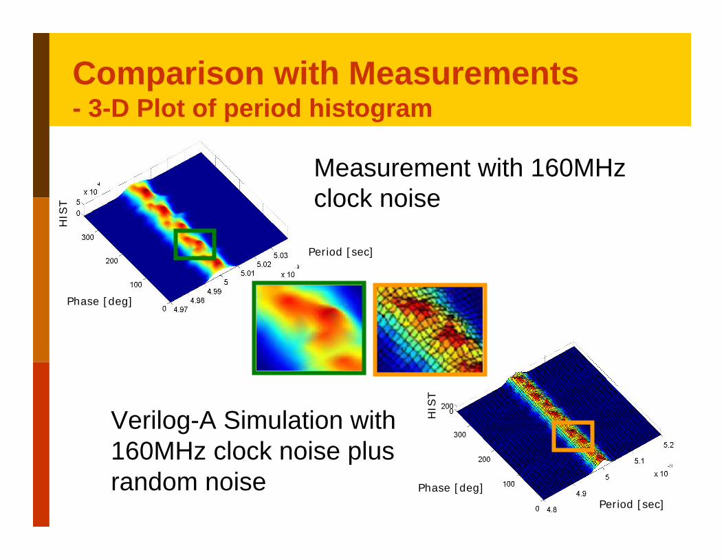
Comparison with Measurements- 3-D Plot of period histogram
Measurement with 160MHz clock noise
Verilog-A Simulation with 160MHz clock noise plus random noise
Phase [deg]
Period [sec]
HIS
T
Phase [deg]Period [sec]
HIS
T
Outline
Introduction
Substrate Noise Coupling Mechanism and Modeling Technique
Comparison between Simulation Methodologies
Period Histogram and Comparison with Measurements
Conclusion
ConclusionImpulse Sensitivity Function (ISF) can be used as the behavioral model of the substrate noise coupling to VCO with a linear and time variant approach.Two versions of Verilog-A are utilized to implement the system level simulation and compared with the transistor level simulation (Hspice).Results from the system level simulation are compared with the measurement results in terms of the period histogram, showing good correlation.