gkmcet lecture plan - · pdf filegkmcet lecture plan ... · the ram memory is used to...
TRANSCRIPT

GKMCETLecture plan
Code & name of subject: 141402 – Microprocessors & MicrocontrollersUnit no: 1
UNIT ITHE 8085 AND 8086 MICROPROCESSORS (9)
8085 Microprocessor architecture-Addressing modes- Instruction set-Programming the8085
1 INTRODUCTION TO MICROPROCESSOR BASED SYSTEMThe microprocessor is a semiconductor device (Integrated Circuit)
manufactured by the VLSI (Very Large Scale Integration) technique. It includes the ALU,register arrays and control circuit on a single chip. To perform a function or useful task we haveto form a system by using microprocessor as a CPU and interfacing memory, input and outputdevices to it. A system designed using a microprocessor as its CPU is called a microcomputer.The Microprocessor based system (single board microcomputer) consists of microprocessor asCPU, semiconductor memories like EPROM and RAM, input device, output device andinterfacing devices. The memories, input device, output device and interfacing devices are calledperipherals. The popular input devices are keyboard and floppy disk and the output devices areprinter, LED/LCD displays, CRT monitor, etc.
The above block diagram shows the organization of a microprocessor based system. In thissystem, the microprocessor is the master and all other peripherals are slaves. The master controlsall the peripherals and initiates all operations.The work done by the processor can be classified into the following three groups.1. Work done internal to the processor2. Work done external to the processor3. Operations initiated by the slaves or peripherals.
www.vidyarthiplus.com
www.vidyarthiplus.com

GKMCETLecture plan
Code & name of subject: 141402 – Microprocessors & MicrocontrollersUnit no: 1The work done internal to the processors is addition, subtraction, logical operations, data transferOperations, etc. The work done external to the processor are reading/writing the memory andReading/writing the J/O devices or the peripherals. If the peripheral requires the attention of themaster then it can interrupt the master and initiate an operation.
The microprocessor is the master, which controls all the activities of the system. To perform aspecific job or task, the microprocessor has to execute a program stored in memory. The programconsists of a set of instructions. It issues address and control signals and fetches the instructionand data from memory. The instruction is executed one by one internal to the processor and basedon the result it takes appropriate action.
BUSES:The buses are group of lines that carries data, address or control signals.· The CPU Bus has multiplexed lines, i.e., same line is used to carry different signals.The CPU interface is provided to demultiplex the multiplexed lines, to generate chip selectsignals and additional control signals.· The system bus has separate lines for each signal.All the slaves in the system are connected to the same system bus. At any time instantcommunication takes place between the master and one of the slaves. All the slaves have tristatelogic and hence normally remain in high impedance state. Only when the slave is selected itcomes to the normal logic.
PERIPHERAL DEVICES:· The EPROM memory is used to store permanent programs and data.· The RAM memory is used to store temporary programs and data.· The input device is used to enter the program, data and to operate the system.· The output device is used for examining the results.Since the speed of I/O devices does not match with the speed of microprocessor, an interfacedevice is provided between system bus and I/O devices. Generally I/O devices are slowdevices.
Advantages of Microprocessor based system1. Computational/processing speed is high.2. Intelligence has been brought to systems.3. Automation of industrial processes and office administration.4. Since the devices are programmable, there is flexibility to alter the system by changing thesoftware alone.5. Less number of components, compact in size and cost less. Also it is more reliable.6. Operation and maintenance are easier.
Disadvantages of Microprocessor based System1. It has limitations on the size of data.2. The applications are limited by the physical address space.3. The analog signals cannot be processed directly and digitizing the analog signals introduceserrors.4. The speed of execution is slow and so real time applications are not possible.5. Most of the microprocessors does not support floating point operations.
www.vidyarthiplus.com
www.vidyarthiplus.com

GKMCETLecture plan
Code & name of subject: 141402 – Microprocessors & MicrocontrollersUnit no: 1
8085 Microprocessor:The salient features of 8085 μp are:
• It is a 8 bit microprocessor.• It is manufactured with N-MOS technology.• It has 16-bit address bus and hence can address up to 216 = 65536 bytes (64KB) memorylocations through A0-A15.• The first 8 lines of address bus and 8 lines of data bus are multiplexed AD0 – AD7.• Data bus is a group of 8 lines D0 – D7.• It supports external interrupt request.• A 16 bit program counter (PC)• A 16 bit stack pointer (SP)• Six 8-bit general purpose register arranged in pairs: BC, DE, HL.• It requires a signal +5V power supply and operates at 3.2 MHZ single phase clock.• It is enclosed with 40 pins DIP (Dual in line package).
ARCHITECTURE:The architecture of.8085 is shown in figure given below. The internal
architecture of 8085 includes the ALU, timing and control unit, instruction register anddecoder, register array, interrupt control and serial I/O control.
www.vidyarthiplus.com
www.vidyarthiplus.com

GKMCETLecture plan
Code & name of subject: 141402 – Microprocessors & MicrocontrollersUnit no: 1
INTEL 8085 – Pin Diagram & Description
www.vidyarthiplus.com
www.vidyarthiplus.com

http:/
/csetu
be.co
.nr/
GKMCETLecture plan
Code & name of subject: 141402 – Microprocessors & MicrocontrollersUnit no: 1
www.vidyarthiplus.com
www.vidyarthiplus.com

http:/
/csetu
be.co
.nr/
GKMCETLecture plan
Code & name of subject: 141402 – Microprocessors & MicrocontrollersUnit no: 1
OPERATIONS PERFORMED BY 8085The ALU performs the arithmetic and logical operations. The operations performed
by ALU of 8085 are addition, subtraction, increment, decrement, logical AND, OR, EXCLU8IVE -OR, compare, complement and left / right shift. The accumulator and temporaryregister are used to hold the data during an arithmetic / logical operation. After an operation theresult is stored in the accumulator and the flags are set or reset according to the result of theoperation.
www.vidyarthiplus.com
www.vidyarthiplus.com

GKMCETLecture plan
Code & name of subject: 141402 – Microprocessors & MicrocontrollersUnit no: 1
FLAG REGISTER:There are five flags in 8085, which are sign flag (8), zero flag (Z), auxiliary carry
flag (AC), parity flag (P) and carry flag (CY). The bit positions reserved for these flags in theflag registerare shown in figure below.
After an ALU operation, if the most significant bit of the result is 1, then sign flag is set. The zeroflag is set, if the ALU operation results in zero and it is reset if the result is non-zero. In anarithmetic operation, when a carry is generated by the lower nibble, the auxiliary carry flag is set.After an arithmetic or logical operation, if the result has an even number of 1 's the parity flag isset, other wise it is reset.If an arithmetic operation results in a carry, the carry flag is set otherwise it is reset. Among the five flags, the AC flag is used internally for BCD arithmetic and otherfour flags can be used by the programmer to check the conditions of the result of an operation.
TIMING & CONTROL UNIT:The timing and control unit synchronizes all the microprocessor operations with the clock andgenerates the control signals necessary for communication between the microprocessor andperipherals.
INSTRUCTION REGISTER & DECODER:When an instruction is fetched from memory it is placed in instruction register. Then it is decodedand encoded into various machine cycles.
REGISTER ARRAY:· Apart from Accumulator (A-register), there are six general-purpose programmable registersB, C, D, E, H and L.· They can be used as 8-bit registers or paired to store l6-bit data. The allowed pairs are B-C,D-E and H-L.· The temporary registers W and Z are intended for internal use of the processor and it cannotbe used by the programmer.
STACK POINTER (SP):The stack pointer SP, holds the address of the stack top. The stack is a sequence of RAMmemory locations defined by the programmer. The stack is used to save the content ofregisters during the execution of a program.
PROGRAM COUNTER (PC):The program counter (PC) keeps track of program execution. To execute a program the
www.vidyarthiplus.com
www.vidyarthiplus.com

GKMCETLecture plan
Code & name of subject: 141402 – Microprocessors & MicrocontrollersUnit no: 1starting address of the program is loaded in program counter. The PC sends out an address tofetch a byte of instruction from memory and increment its content automatically. Hence,when a byte of instruction is fetched, the PC holds the address of the next byte of theinstruction or next instruction.Memory• Program, data and stack memories occupy the same memory space. The total addressablememory size is 64 KB.• Program memory - program can be located anywhere in memory. Jump, branch and callinstructions use 16-bit addresses, i.e. they can be used to jump/branch anywhere within 64 KB.All jump/branch instructions use absolute addressing.• Data memory - the processor always uses 16-bit addresses so that data can be placed anywhere.• Stack memory is limited only by the size of memory. Stack grows downward.• First 64 bytes in a zero memory page should be reserved for vectors used by RST instructions.
Interrupts• The processor has 5 interrupts. They are presented below in the order of their priority (fromlowest to highest):• INTR is maskable 8080A compatible interrupt. When the interrupt occurs the processor fetchesfrom the bus one instruction, usually one of these instructions:• One of the 8 RST instructions (RST0 - RST7). The processor saves current program counterinto stack and branches to memory location N * 8 (where N is a 3-bit number from 0 to 7supplied with the RST instruction).• CALL instruction (3 byte instruction). The processor calls the subroutine, address of which isspecified in the second and third bytes of the instruction.• RST5.5 is a maskable interrupt. When this interrupt is received the processor saves the contentsof the PC register into stack and branches to 2CH (hexadecimal) address.• RST6.5 is a maskable interrupt. When this interrupt is received the processor saves the contentsof the PC register into stack and branches to 34H (hexadecimal) address.• RST7.5 is a maskable interrupt. When this interrupt is received the processor saves the contentsof the PC register into stack and branches to 3CH (hexadecimal) address.• TRAP is a non-maskable interrupt. When this interrupt is received the processor saves thecontents of the PC register into stack and branches to 24H (hexadecimal) address.• All maskable interrupts can be enabled or disabled using EI and DI instructions. RST 5.5,RST6.5 and RST7.5 interrupts can be enabled or disabled individually using SIM instruction.
Reset Signals• RESET IN: When this signal goes low, the program counter (PC) is set to Zero, μp is reset andresets the interrupt enable and HLDA flip-flops.• The data and address buses and the control lines are 3-stated during RESET and because ofasynchronous nature of RESET, the processor internal registers and flags may be altered byRESET with unpredictable results.• RESET IN is a Schmitt-triggered input, allowing connection to an R-C network for power-onRESET delay.• Upon power-up, RESET IN must remain low for at least 10 ms after minimum Vcc has beenreached.• For proper reset operation after the power – up duration, RESET IN should be kept low aminimum of three clock periods.
www.vidyarthiplus.com
www.vidyarthiplus.com

GKMCETLecture plan
Code & name of subject: 141402 – Microprocessors & MicrocontrollersUnit no: 1• The CPU is held in the reset condition as long as RESET IN is applied. Typical Power-onRESET RC values R1 = 75KΩ, C1 = 1μF.
• RESET OUT: This signal indicates that μp is being reset. This signal can be used to reset otherdevices. The signal is synchronized to the processor clock and lasts an integral number of clockperiods.
Serial communication Signal• SID - Serial Input Data Line: The data on this line is loaded into accumulator bit 7 whenever aRIM instruction is executed.• SOD – Serial Output Data Line: The SIM instruction loads the value of bit 7 of theaccumulator into SOD latch if bit 6 (SOE) of the accumulator is 1.
DMA Signals• HOLD: Indicates that another master is requesting the use of the address and data buses. TheCPU, upon receiving the hold request, will relinquish the use of the bus as soon as the completionof the current bus transfer.• Internal processing can continue. The processor can regain the bus only after the HOLD isremoved.• When the HOLD is acknowledged, the Address, Data RD, WR and IO/M lines are 3-stated.• HLDA: Hold Acknowledge: Indicates that the CPU has received the HOLD request and that itwill relinquish the bus in the next clock cycle.• HLDA goes low after the Hold request is removed. The CPU takes the bus one half-clock cycleafter HLDA goes low.• READY: This signal Synchronizes the fast CPU and the slow memory, peripherals.• If READY is high during a read or write cycle, it indicates that the memory or peripheral isready to send or receive data.• If READY is low, the CPU will wait an integral number of clock cycle for READY to go highbefore completing the read or write cycle.• READY must conform to specified setup and hold times.
Registers• Accumulator or A register is an 8-bit register used for arithmetic, logic, I/O and load/storeoperations.• Flag Register has five 1-bit flags.• Sign - set if the most significant bit of the result is set.• Zero - set if the result is zero.• Auxiliary carry - set if there was a carry out from bit 3 to bit 4 of the result.• Parity - set if the parity (the number of set bits in the result) is even.• Carry - set if there was a carry during addition, or borrow duringsubtraction/comparison/rotation.
General Registers• 8-bit B and 8-bit C registers can be used as one 16-bit BC register pair. When used as a pairthe C register contains low-order byte. Some instructions may use BC register as a datapointer.
www.vidyarthiplus.com
www.vidyarthiplus.com

GKMCETLecture plan
Code & name of subject: 141402 – Microprocessors & MicrocontrollersUnit no: 1• 8-bit D and 8-bit E registers can be used as one 16-bit DE register pair. When used as a pairthe E register contains low-order byte. Some instructions may use DE register as a datapointer.• 8-bit H and 8-bit L registers can be used as one 16-bit HL register pair. When used as a pairthe L register contains low-order byte. HL register usually contains a data pointer used toreference memory addresses.• Stack pointer is a 16 bit register. This register is always decremented/incremented by 2during push and pop.• Program counter is a 16-bit register.
INSTRUCTION EXECUTION AND DATA FLOW in 8085The program instructions are stored in memory, which is an external device. To execute
a program in 8085, the starting address of the program should be loaded in program counter. The8085 output the content of program counter in address bus and asserts read control signal low.Also, the program counter is incremented.The address and the read control signal enable thememory to output the content of memory location on the data bus. Now the content of data bus isthe opcode of an instruction. The read control signal is made high by timing and control unit aftera specified time. At the rising edge of read control signals, the opcode is latched intomicroprocessor internal bus and placed in instruction register.The instruction-decoding unit, decodes the instructions and provides information to timing andcontrol unit to take further actions.INSTRUCTION FORMAT OF 8085The 8085 have 74 basic instructions and 246 total instructions. The instruction set of 8085 isdefined by the manufacturer Intel Corporation. Each instruction of 8085 has 1 byte opcode. With8 bit binary code, we can generate 256 different binary codes. In this, 246 codes have been usedfor opcodes.
The size of 8085 instructions can be 1 byte, 2 bytes or 3 bytes.· The 1-byte instruction has an opcode alone.· The 2 bytes instruction has an opcode followed by an eight-bit address or data.· The 3 bytes instruction has an opcode followed by 16 bit address or data. While storing the 3bytes instruction in memory, the sequence of storage is, opcode first followed by low byte ofaddress or data and then high byte of address or data.
ADDRESSING MODESEvery instruction of a program has to operate on a data. The method of specifying the
data to be operated by the instruction is called Addressing. The 8085 has the following 5 differenttypes of addressing.
www.vidyarthiplus.com
www.vidyarthiplus.com

GKMCETLecture plan
Code & name of subject: 141402 – Microprocessors & MicrocontrollersUnit no: 11. Immediate Addressing2. Direct Addressing3. Register Addressing4. Register Indirect Addressing5. Implied AddressingImmediate AddressingIn immediate addressing mode, the data is specified in the instruction itself. The data will be apartof the program instruction. All instructions that have ‘I’ in their mnemonics are of Immediateaddressing type.Eg. MVI B, 3EH - Move the data 3EH given in the instruction to B register.
Direct AddressingIn direct addressing mode, the address of the data is specified in the instruction. The data will bein memory. In this addressing mode, the program instructions and data can be stored in differentmemory blocks. This type of addressing can be identified by 16-bit address present in theinstruction.Eg. LDA 1050H - Load the data available in memory location 1050H in accumulator.
Register AddressingIn register addressing mode, the instruction specifies the name of the register in which the data isavailable. This type of addressing can be identified by register names (such as ‘A’, ‘B’, … ) in theinstruction.Eg. MOV A, B -Move the content of B register to A register.
Register Indirect AddressingIn register indirect addressing mode, the instruction specifies the name of the register in which theaddress of the data is available. Here the data will be in memory and the address will be in theregister pair. This type of addressing can be identified by letter ‘M’ present in the instruction.Eg. MOV A, M - The memory data addressed by HL pair is moved to A register.
Implied AddressingIn implied addressing mode, the instruction itself specifies the type of operation and location ofdata to be operated. This type of instruction does not have any address, register name, immediatedata specified along with it.Eg. CMA - Complement the content of accumulator.
INSTRUCTION SETThe 8085 instruction set can be classified into the following five functional headings.Group I - DATA TRANSFER INSTRUCTIONS:Includes the instructions that moves ( copies) data between registers or between memorylocations and registers. In all data transfer operations the content of source register is not altered.Hence the data transfer is copying operation.Ex: i) MOV A,B ii) LDA 4600 iii) LHLD 4200
Group II - ARITHMETIC INSTRUCTIONS:Includes the instructions which performs the addition, subtraction, increment or decrementoperations. The flag conditions are altered after execution of an instruction in this group.Ex: i) ADD B ii) SUB C iii) INR D iv) INX H
www.vidyarthiplus.com
www.vidyarthiplus.com
GKMCETLecture plan
Code & name of subject: 141402 – Microprocessors & MicrocontrollersUnit no: 1Group III - LOGICAL INSTRUCTIONS:The instructions which performs the logical operations like AND, OR, Exclusive-OR,complement, compare and rotate instructions are grouped under this heading. The flag conditionsare altered after execution of an instruction in this group.Ex: i) ORA B ii) XRA A iii) RAR
Group IV - BRANCHING INSTRUCTIONS:The instructions that are used to transfer the program control from one memory location toanother memory location are grouped under this heading.Ex: i) JZ 4200 ii) RST 7 iii) CALL 4300
Group V - MACHINE CONTROL INSTRUCTIONS:Includes the instructions related to interrupts and the instruction used to halt program execution.Ex: i) SIM ii) RIM iii) HLT
The 74 basic instructions of8085 are listed inTable. The opcode of each instruction, size,machine cycles, number of T -state and the total number of instructions in each type are alsoshown in table in next page. The instructions affecting the status flag are listed in table followed
www.vidyarthiplus.com
www.vidyarthiplus.com

http:/
/csetu
be.co
.nr/
GKMCETLecture plan
Code & name of subject: 141402 – Microprocessors & MicrocontrollersUnit no: 1
www.vidyarthiplus.com
www.vidyarthiplus.com

http:/
/csetu
be.co
.nr/
GKMCETLecture plan
Code & name of subject: 141402 – Microprocessors & MicrocontrollersUnit no: 1
www.vidyarthiplus.com
www.vidyarthiplus.com

http:/
/csetu
be.co
.nr/
GKMCETLecture plan
Code & name of subject: 141402 – Microprocessors & MicrocontrollersUnit no: 1
www.vidyarthiplus.com
www.vidyarthiplus.com

http:/
/csetu
be.co
.nr/
GKMCETLecture plan
Code & name of subject: 141402 – Microprocessors & MicrocontrollersUnit no: 1
TIMING DIAGRAM for various machine cyclesThe machine cycles are the basic operations performed by the processor, while
instructions are executed. The time taken for performing each machine cycle is expressed interms of Tstates. One T-state is the time period of one clock cycle of the microprocessor.The various machine cycles are1. Opcode fetch …………….. - 4 / 6 T2. Memory Read ……………. - 3 T3. Memory Write ……………. - 3 T4. I/O Read ………………….. - 3 T5. I/O Write …………………. - 3 T6. Interrupt Acknowledge …… - 6 / 12 T7. Bus Idle …………………… - 2 / 3 T
www.vidyarthiplus.com
www.vidyarthiplus.com

http:/
/csetu
be.co
.nr/
GKMCETLecture plan
Code & name of subject: 141402 – Microprocessors & MicrocontrollersUnit no: 1
www.vidyarthiplus.com
www.vidyarthiplus.com

GKMCETLecture plan
Code & name of subject: 141402 – Microprocessors & MicrocontrollersUnit no: 1
PROGRAMMING EXAMPLES:1. Write an ALP using 8085 to multiply two 8-bit numbers by repeated addition.MVI A, OO ; Accumulator contents are clearedMVI C, OO ; C Register contents are clearedMVI B, data#1 ; I Operand is loaded into B RegisterMVI D, data#2 ; II Operand is loaded into D RegisterLoop: ADD B |JNC next |INR C } Multiplication by repeated addition.Next: DCR D |JNZ loop |STA 4200H ; Storing of results into memory locationMOV A,CSTA 4201H ; Storing of carry into next memory location
3. Write an ALP using 8085 to evaluate the expression C=A2+B2
Let ‘A’ be Data#1 and ‘B’ be Data#2MVI B, Data#1 ; Data #1 is stored in register BMOV C, B ; Copy of Data #1 is made in register CMVI D, Data#2 ; Data #2 is stored in register DMOV E,D ; Copy of Data #2 is made in register EXRA A ; Accumulator content is clearedAgain: ADD B ]DCR C } A2 is calculated by repeated AdditionJNZ Again ]MOV H,A ; Calculated A2 value is stored in register HXRA A ; Accumulator content is clearedLoop: ADD D ]DCR E } B2 is calculated by repeated AdditionJNZ Loop ]ADD H ; A2+ B2 is determined,
by adding result in A
www.vidyarthiplus.com
www.vidyarthiplus.com

GKMCETLecture plan
Code & name of subject: 141402 – Microprocessors & MicrocontrollersUnit no: 1
and register content HSTA 4200H ; Result is stored in memory location 4200H
www.vidyarthiplus.com
www.vidyarthiplus.com

GKMCETLecture plan
Code & name of subject: 141402 – Microprocessors & MicrocontrollersUnit no: 2
UNIT II8086 SOFTWARE ASPECTS 9Intel 8086 microprocessor -Architecture - Signals- Instruction Set-Addressing Modes-Assembler
Directives- Assembly Language Programming-Procedures-Macros-InterruptsAnd Interrupt ServiceRoutines-BIOS function calls.Introduction to 8086 MicroprocessorFeatures: Intel 8086 was launched in 1978. It was the first 16-bit microprocessor. This microprocessor had major improvement over the execution speed of 8085. It is available as 40-pin Dual-Inline-Package (DIP). It is available in three versions:
a. 8086 (5 MHz)b. 8086-2 (8 MHz)c. 8086-1 (10 MHz)
It consists of 29,000 transistors.Architecture of 8086 Microprocessor
www.vidyarthiplus.com
www.vidyarthiplus.com

http:/
/csetu
be.co
.nr/
GKMCETLecture plan
Code & name of subject: 141402 – Microprocessors & MicrocontrollersUnit no: 2
Bus Interface Unit (BIU):The function of BIU is toFetch the instruction or data from memory.Write the data to memory.Write the data to the port.Read data from the port.
Instruction Queue1. To increase the execution speed, BIU fetches as many as six instruction bytesahead to time from memory.2. All six bytes are then held in first in first out 6 byte register called instructionqueue.3. Then all bytes have to be given to EU one by one.4. This pre fetching operation of BIU may be in parallel with execution operation ofEU, which improves the speed execution of the instruction.
www.vidyarthiplus.com
www.vidyarthiplus.com

GKMCETLecture plan
Code & name of subject: 141402 – Microprocessors & MicrocontrollersUnit no: 2
Execution Unit (EU)The functions of execution unit areTo tell BIU where to fetch the instructions or data from.To decode the instructions.To execute the instructions.
The EU contains the control circuitry to perform various internal operations. A decoder inEU decodes the instruction fetched memory to generate different internal or external controlsignals required to perform the operation. EU has 16-bit ALU, which can perform arithmetic andlogical operations on 8-bit as well as 16-bit.
General Purpose Registers of 8086These registers can be used as 8-bit registers individually or can be used as 16-bit in
pair to have AX,BX, CX, and DX.1. AX Register: AX register is also known as accumulator register that stores operands forarithmetic operation like divided, rotate.2. BX Register: This register is mainly used as a base register. It holds the starting baselocation of a memory region within a data segment.3. CX Register: It is defined as a counter. It is primarily used in loop instruction to store loopcounter.4.DX Register: DX register is used to contain I/O port address for I/O instruction.
Segment RegistersAdditional registers called segment registers generate memory address when combined
with other in the microprocessor. In 8086 microprocessor, memory is divided into 4 segments asfollow:
1. Code Segment (CS): The CS register is used for addressing a memory location in the CodeSegment of the memory, where the executable program is stored.
www.vidyarthiplus.com
www.vidyarthiplus.com

GKMCETLecture plan
Code & name of subject: 141402 – Microprocessors & MicrocontrollersUnit no: 22. Data Segment (DS): The DS contains most data used by program. Data are accessed in theData Segment by an offset address or the content of other register that holds the offsetaddress.3. Stack Segment (SS): SS defined the area of memory used for the stack.4. Extra Segment (ES): ES is additional data segment that is used by some of the string to holdthe destination data.
Flag Registers of 8086:
Flags Register determines the current state of the processor. They are modified automatically byCPU after mathematical operations, this allows to determine the type of the result, and todetermine conditions to transfer control to other parts of the program. 8086 has 9 flags and theyare divided into two categories:1. Conditional Flags2. Control Flags(1) Conditional FlagsConditional flags represent result of last arithmetic or logical instruction executed. Conditionalflags are as follows:Carry Flag (CF)This flag indicates an overflow condition for unsigned integer arithmetic.It is also used inmultiple-precision arithmetic.Auxiliary Flag (AF):If an operation performed in ALU generates a carry/barrow from lower nibble (i.e. D0 D3)to upper nibble (i.e. D4 – D7), the AF flag is set i.e. carry given by D3 bit to D4 is AF flag. Thisis not a general-purpose flag, it is used internally by the processor to perform Binary to BCDconversion.Parity Flag (PF):This flag is used to indicate the parity of result. If lower order 8-bits of the result contains evennumber of 1‟s, the Parity Flag is set and for odd number of 1‟s, the Parity Flag is reset.Zero Flag (ZF):It is set; if the result of arithmetic or logical operation is zero else it is reset.Sign Flag (SF):In sign magnitude format the sign of number is indicated by MSB bit. If theresult of operation is negative, sign flag is set.Overflow Flag (OF):It occurs when signed numbers are added or subtracted. An OF indicates that the result hasexceeded the capacity of machine.Control FlagsControl flags are set or reset deliberately to control the operations of the execution unit.
www.vidyarthiplus.com
www.vidyarthiplus.com
GKMCETLecture plan
Code & name of subject: 141402 – Microprocessors & MicrocontrollersUnit no: 2Control flags are as follows:1. Trap Flag (TP): It is used for single step control. It allows user to execute one instruction of a program at a time for debugging. When trap flag is set, program can be run in single step mode.
2. Interrupt Flag (IF): It is an interrupt enable/disable flag. If it is set, the maskable interrupt of 8086 is enabled and if it is reset, the interrupt is disabled. It can be set by executing instruction sit and can be cleared by executing CLI instruction.
3. Direction Flag (DF): It is used in string operation. If it is set, string bytes are accessed from higher memory address to lower memory address. When it is reset, the string bytes are accessed from lower memory address to higher memory address.
8086-Minimum mode of operation
www.vidyarthiplus.com
www.vidyarthiplus.com

http:/
/csetu
be.co
.nr/
GKMCETLecture plan
Code & name of subject: 141402 – Microprocessors & MicrocontrollersUnit no: 2
Minimum Mode InterfaceAddress/Data bus: 20 bits vs 8 bits multiplexedStatus signals: A16-A19 multiplexed with status signals S3-S6 respectively.S3 and S4 together
form a 2 bit binary code that identifies which of the internal segment registers was used togenerate the physical address that was output on the address bus during the current bus cycle.S5 is the logic level of the internal interrupt enable flag, S6 is always logic 0.Control Signals:
Address Latch Enable (ALE) is a pulse to logic 1 that signals external circuitry when avalid address is on the bus. This address can be latched in external circuitry on the 1-to-0edge of the pulse at ALE.IO/M line: memory or I/O transfer is selected (complement for 8086)DT/R line: direction of data is selectedSSO (System Status Output) line: =1 when data is read from memory and =0 whencode is read from memory (only for 8088)BHE (Bank High Enable) line : =0 for most significant byte of data for 8086 and alsocarries S7RD line: =0 when a read cycle is in progressWR line: =0 when a write cyle is in progressDEN line: (Data enable) Enables the external devices to supply data to the processor.Ready line: can be used to insert wait states into the bus cycle so that it is extended by anumber of clock periods
www.vidyarthiplus.com
www.vidyarthiplus.com
GKMCETLecture plan
Code & name of subject: 141402 – Microprocessors & MicrocontrollersUnit no: 2Interrupt signals:
INTR (Interrupt request) :=1 shows there is a service request, sampled at the finalclock cycle of each instruction acquisition cycle.INTA : Processor responds with two pulses going to 0 when it services the interrupt andwaits for the interrupt service number after the second pulse.TEST: Processor suspends operation when =1. Resumes operation when=0. Used tosyncronize the processor to external events.NMI (Nonmaskable interrupt) : A leading edge transition causes the processor go tothe interrupt routine after the current instruction is executed.RESET : =0 Starts the reset sequence.
Maximum Mode Interface• For multiprocessor environment• 8288 Bus Controller is used for bus control• WR¯,IO/M¯,DT/R¯,DEN¯,ALE, INTA¯ signals are not available.
o MRDC¯ (memory read command)o MWRT¯ (memory write command)o AMWC¯ (advanced memory write command)o IORC¯ (I/O read command)o IOWC¯ (I/O write command)o AIOWC¯ (Advanced I/O write command)o INTA¯ (interrupt acknowledge)
www.vidyarthiplus.com
www.vidyarthiplus.com

http:/
/csetu
be.co
.nr/
GKMCETLecture plan
Code & name of subject: 141402 – Microprocessors & MicrocontrollersUnit no: 2
Addressing ModesA] Data Category B] Branch Category
Data Category:1)Immediate Addressing 2) Direct Addressing ( Segment Override prefix) 3) Registeraddressing 4) Register Indirect Addressing . 5)Register relative addressing.6)Base Indexaddressing 7)Relative base index addressing.
Branch Category:1) IntrasegmentDirect 2) IntersegmentIndirect.
Instruction SetWe only cover the small subset of the 8088 instruction set that is essential. In particular, we willnot mention various registers, addressing modes and instructions that could often provide fasterways of doing things.A summary of the 80x86 protected-mode instruction set is available on thecourse Web page and should be printed out if you don’t have another reference.
Data Transfer
www.vidyarthiplus.com
www.vidyarthiplus.com

GKMCETLecture plan
Code & name of subject: 141402 – Microprocessors & MicrocontrollersUnit no: 2The MOV instruction is used to transfer 8 and 16-bit data to and from registers. Either the sourceor destination has to be a register. The other operand can come from another register, frommemory, from immediate data (a value included in the instruction) or from a memory location“pointed at” by register BX.
For example, if COUNT is the label of a memory location the following are possible assembly-language instructions :
; register: move contents of BX to AXMOV AX,BX
; direct: move contents of AX to memoryMOV COUNT,AX
; immediate: load CX with the value 240MOV CX,0F0H
; memory: load CX with the value at; address 240MOV CX,[0F0H]
; register indirect: move contents of AL; to memory location in BXMOV [BX],AL
Most 80x86 assemblers keep track of the type of each symbol and require a type “override” whenthe symbol is used in a different way. The OFFSET operator to convert a memory reference to a16-bit value.
For example:MOV BX,COUNT ; load the value at location COUNTMOV BX,OFFSET COUNT ; load the offset of COUNT16-bit registers can be pushed (the SP is first decremented by two and then the value stored at SP)or popped (the value is restored from the memory at SP and then SP is incremented by 2).
For example:PUSH AX ; push contents of AXPOP BX ; restore into BX
There are some things to note about Intel assembly language syntax: the order of the operands is destination,source —the reverse of that used on the 68000! semicolons begin a comment the suffix ’H’ is used to indicate a hexadecimal constant, if the constant begins with a letter it must be prefixed with a zero to distinguish it from a label the suffix ’B’ indicates a binary constant square brackets indicate accesses to memory the size of the transfer (byte or word) is determined
www.vidyarthiplus.com
www.vidyarthiplus.com

GKMCETLecture plan
Code & name of subject: 141402 – Microprocessors & MicrocontrollersUnit no: 2
by the size of the destination
I/O OperationsThe 8086 has separate I/O and memory address spaces. Values in the I/O space are accessed withIN and OUT instructions. The port address is loaded into DX and the data is read/written to/fromAL or AX:MOV DX,372H ; load DX with port addressOUT DX,AL ; output byte in AL to port ; 372 (hex)IN AX,DX ; input word to AX
Arithmetic/LogicArithmetic and logic instructions can be performed on byte and 16-bit values. The first operandhas to be a register and the result is stored in that register.; increment BX by 4ADD BX,4; subtract 1 from ALSUB AL,1; increment BXINC BX; compare (subtract and set flags ; but without storing result)CMP AX,[MAX]; mask in LS 4 bits of ALAND AL,0FH; divide AX by twoSHR AX; set MS bit of CXOR CX,8000H; clear AXXOR AX,AX
Control TransferConditional jumps transfer control to another address depending on the values of the flags in theflag register. Conditional jumps are restricted to a range of -128 to +127 bytes from the nextinstruction while unconditional jumps can be to any point.; jump if last result was zero (two values equal)JZ skip; jump if carry set (below)JC neg; jump on carry not setJNC smaller; unconditional jump:JMP loopThe assembly-language equivalent of an if statement in a high-level language is a CoMPareoperation followed by a conditional jump.
The CALL and RET instructions call and return from subroutines. The processor pushes IP on thestack during a CALL instruction and the contents of IP are popped by the RET instructions.For example:
www.vidyarthiplus.com
www.vidyarthiplus.com

GKMCETLecture plan
Code & name of subject: 141402 – Microprocessors & MicrocontrollersUnit no: 2CALL readchar...readchar:...RET
Segment/Offset AddressingSince address registers and address operands are only 16 bits they can only address 64k bytes. Inorder to address the 20-bit address range of the 8086, physical addresses (those that are put on theaddress bus) are always formed by adding the values of one of the segment registers to the 16-bitaddress to form a 20- bit address. The segment registers themselves only contain themost-significant 16 bits of the 20-bit value that is contributed by the segment registers. The leastsignificant four bits of the segment address are always zero.
By default, the DS (data segment) is used for data transfer instructions (e.g. MOV), CS (codesegment) is used with control transfer instructions (e.g. JMP or CALL), and SS is used with thestack pointer (e.g. PUSH or to save/restore addresses during CALL/RET or INT instructions).
The use of segment registers reduces the size of pointers to 16 bits. This reduces the code size butalso restricts the addressing range of a pointer to 64k bytes. Performing address arithmetic withindata structures larger than 64k is awkward. This is the biggest drawback of the 8086 architecture.We will restrict ourselves to short programs where all of the code, data and stack are placed intothe same 64k segment (i.e. CS=DS=SS).
Interrupts and ExceptionsIn addition to interrupts caused by external events (such as an IRQ signal), certain instructionssuch as a dividing by zero or the INT instruction generate exceptions.The 8086 reserves the lower 1024 bytes of memory for an interrupt vector table. There is one4-byte vector for each of the 256 possible interrupt/exception numbers. When an interrupt orexception occurs, the processor: (1) clears the interrupt flag in the flags register, (2) pushes theflags register, CS, and IP (in that order), (3) loads IP and CS (in that order) from the appropriateinterrupt vector location, and (4) transfers control to that location. For external interrupts (IRQ orNMI) the interrupt number is read from the data bus during an interrupt acknowledge bus cycle.For internal interrupts (e.g. INT instruction) the interrupt number is determined from theinstruction.The INT instruction allows a program to generate any of the 256 interrupts. This“software interrupt” is typically used to access operating system services.
Pseudo-OpsA number of assembler directives (“pseudo-ops”) are also required to write assembly languageprograms.ORG specifies the location of code or data within the segment, DB and DW assemblebytes and words of constant data respectively.
Assembler Directives :
ASSUME DB - Defined Byte.
www.vidyarthiplus.com
www.vidyarthiplus.com
GKMCETLecture plan
Code & name of subject: 141402 – Microprocessors & MicrocontrollersUnit no: 2
DD - Defined Double Word DQ - Defined Quad Word DT - Define Ten Bytes DW - Define Word
ASSUME Directive - The ASSUME directive is used to tell the assembler that the name of thelogical segment should be used for a specified segment. The 8086 works directly with only 4physical segments: a Code segment, a data segment, a stack segment, and an extra segment.
Example:ASUME CS:CODE ;This tells the assembler that the logical segment named CODE contains theinstruction statements for the program and should be treated as a code segment.ASUME DS:DATA ;This tells the assembler that for any instruction which refers to a data in thedata segment, data will found in the logical segment DATA.
DB - DB directive is used to declare a bytetype variable or to store a byte in memory location.Example:1. PRICE DB 49h, 98h, 29h ;Declare an array of 3 bytes, named as PRICE and initialize.2. NAME DB ‘ABCDEF’ ;Declare an array of 6 bytes and initialize with ASCII code for letters3. TEMP DB 100 DUP(?) ;Set 100 bytes of storage in memory and give it the name as TEMP,but leave the 100 bytes uninitialized. Program instructions will load values into these locations.
DW - The DW directive is used to define a variable of type word or to reserve storage location oftype word in memory.Example:MULTIPLIER DW 437Ah ; this declares a variable of type word and named it asMULTIPLIER. This variable is initialized with the value 437Ah when it is loadedinto memory to run.EXP1 DW 1234h, 3456h, 5678h ; this declares an array of 3 words and initialized with specifiedvalues.STOR1 DW 100 DUP(0); Reserve an array of 100 words of memory and initialize all wordswith 0000.Array is named as STOR1.
END - END directive is placed after the last statement of a program to tell the assembler that thisis the end of the program module. The assembler will ignore any statement after an ENDdirective. Carriage return is required after the END directive.
ENDP - ENDP directive is used along with the name of the procedure to indicate the end of aprocedure to the assembler.Example:SQUARE_NUM PROCE ; It start the procedure ;Some steps to find the square root of a numberSQUARE_NUM ENDP ;Hear it is the End for the procedure.
END - End ProgramENDP - End ProcedureENDS - End SegmentEQU - EquateEVEN - Align on Even Memory Address
www.vidyarthiplus.com
www.vidyarthiplus.com

GKMCETLecture plan
Code & name of subject: 141402 – Microprocessors & MicrocontrollersUnit no: 2EXTRN
ENDS - This ENDS directive is used with name of the segment to indicate the end of that logicsegment.Example:CODE SEGMENT ;Hear it Start the logic segment containing code Some instructionsstatements to perform the logical operation.CODE ENDS ;End of segment named as CODE
EQU - This EQU directive is used to give a name to some value or to a symbol. Each time theassembler finds the name in the program, it will replace the name with the value or symbol yougiven to that name.Example:FACTOR EQU 03H ; you has to write this statement at the starting of your program and later inthe program you can use this as followsADD AL, FACTOR ; When it codes this instruction the assembler will code it as ADDAL, 03HThe advantage of using EQU in this manner is, if FACTOR is used many no of times in aprogram and you want to change the value, all you had to do is change the EQU statement atbeginning, it will changes the rest of all.
EVEN - This EVEN directive instructs the assembler to increment the location of the counter tothe next even address if it is not already in the even address. If the word is at even address 8086can read a memory in 1 bus cycle.If the word starts at an odd address, the 8086 will take 2 buscycles to get the data. A series of words can be read much more quickly if they are at evenaddress. When EVEN is used the location counter will simply incremented to next address andNOP instruction is inserted in that incremented location.
Example:DATA1 SEGMENT ; Location counter will point to 0009 after assembler reads next statementSALES DB 9 DUP(?) ;declare an array of 9 bytesEVEN ; increment location counter to 000AHRECORD DW 100 DUP( 0 ) ;Array of 100 words will start from an even address for quickerread
DATA1 ENDSGROUP - Group Related SegmentsLABLENAMEOFFSETORG – Originate
GROUP - The GROUP directive is used to group the logical segments named after the directiveinto one logical group segment.INCLUDE - This INCLUDE directive is used to insert a block of source code from the namedfile into the current source module.
PROC - ProcedurePTR - Pointer
www.vidyarthiplus.com
www.vidyarthiplus.com
GKMCETLecture plan
Code & name of subject: 141402 – Microprocessors & MicrocontrollersUnit no: 2PUBLCSEGMENTSHORTTYPE
PROC - The PROC directive is used to identify the start of a procedure. The term near or far isused to specify the type of the procedure.Example:SMART PROC FAR ; This identifies that the start of a procedure named as SMART andinstructs the assembler that the procedure is far .SMART ENDP This PROC is used with ENDP to indicate the break of the procedure.
PTR - This PTR operator is used to assign a specific type of a variable or to a label.Example:INC [BX] ; This instruction will not know whether to increment the byte pointed to by BX or aword pointed to by BX.INC BYTE PTR [BX] ;increment the byte pointed to by BX This PTR operator can also be usedto override the declared type of variable . If we want to access the a byte in an arrayWORDS DW 437Ah, 0B97h,MOV AL, BYTE PTR WORDS
PUBLIC - The PUBLIC directive is used to instruct the assembler that a specified name or labelwill be accessed from other modules.Example:PUBLIC DIVISOR, DIVIDEND ;these two variables are public so these are available to allmodules.If an instruction in a module refers to a variable in another assembly module, we canaccess that module by declaring as EXTRN directive.
TYPE - TYPE operator instructs the assembler to determine the type of a variable anddetermines the number of bytes specified to that variable.Example:Byte type variable – assembler will give a value 1Word type variable – assembler will give a value 2Double word type variable – assembler will give a value 4ADD BX, TYPE WORD_ ARRAY ; hear we want to increment BX to point to next word in anarray of words.
MACROS:Macros are just like procedures, but not really. Macros =ook like procedures, but they exist onlyuntil your code is compiled, after = compilation all macros are replaced with real instructions. Ifyou = declared a macro and never used it in your code, compiler will =imply ignore it.emu8086.inc is a good example of how macros can be used, this file contains =everal macros tomake coding easier for you.
Macro definition:
name MACRO [parameters,...]
www.vidyarthiplus.com
www.vidyarthiplus.com

GKMCETLecture plan
Code & name of subject: 141402 – Microprocessors & MicrocontrollersUnit no: 2
<instructions>
ENDM
Unlike procedures, macros should be defined above the code that uses it, for example: =
MyMacro MACRO p1, p2, p3
MOV AX, p1MOV BX, p2MOV CX, p3
ENDM
ORG 100h
MyMacro 1, 2, 3
MyMacro 4, 5, DX
RET
The above code is expanded into:
MOV AX, 00001hMOV =X, 00002hMOV CX, 00003hMOV AX, 00004hMOV BX, =0005hMOV CX, DX
Some important facts about macros and procedures:
When you want to use a procedure you should use =B>CALL instruction, for example:
CALL MyProc =/FONT>
When you want to use a macro, you can just type its =ame. For example:
MyMacro =/FONT>
Procedure is located at some specific address in memory, and if you use the sameprocedure 100 times, the CPU will transfer control to this part of the memory. The
www.vidyarthiplus.com
www.vidyarthiplus.com

GKMCETLecture plan
Code & name of subject: 141402 – Microprocessors & MicrocontrollersUnit no: 2
control will be returned back to the program by RET instruction. The =B>stack is used tokeep the return address. The CALL instruction takes about 3 bytes, so the size of theoutput executable file =rows very insignificantly, no matter how many time the procedureis used.
Macro is expanded directly in program's code. So if =ou use the same macro 100 times,the compiler expands the macro =00 times, making the output executable file larger andlarger, each time all instructions of a macro are inserted.
You should use stack or any general purpose registers to pass parameters to procedure.
To pass parameters to macro, you can just type them after the macro name. For example:
MyMacro 1, 2, 3
To mark the end of the macro ENDM directive is enough.
To mark the end of the procedure, you should type the same of the procedure before theENDP directive.
Macros are expanded directly in code, therefore if there are labels inside the macro definition youmay get "Duplicate declaration" error when macro is used for twice or more. To avoid suchproblem, use LOCAL directive followed by names of variables, labels or procedure names. Forexample:
MyMacro2 MACROLOCAL label1, label2
CMP AX, 2JE label1CMP AX, 3JE label2label1:
INC AXlabel2:
ADD AX, 2ENDM
ORG 100h
MyMacro2
www.vidyarthiplus.com
www.vidyarthiplus.com

GKMCETLecture plan
Code & name of subject: 141402 – Microprocessors & MicrocontrollersUnit no: 2
MyMacro2
RET
AN INTRODUCTION TO INTERRUPTS
INTERRUPTS
There are two main types of interrupt in the 8086 microprocessor, internal and external hardwareinterrupts. Hardware interrupts occur when a peripheral device asserts an interrupt input pin ofthe microprocessor. Whereas internal interrupts are initiated by the state of the CPU (e.g. divideby zero error) or by an instruction.
Provided the interrupt is permitted, it will be acknowledged by the processor at the end of thecurrent memory cycle. The processor then services the interrupt by branching to a special serviceroutine written to handle that particular interrupt. Upon servicing the device, the processor is theninstructed to continue with what is was doing previously by use of the "return from interrupt"instruction.
The status of the programme being executed must first be saved. The processors registers will besaved on the stack, or, at very least, the programme counter will be saved. Preserving thoseregisters which are not saved will be the responsibility of the interrupt service routine. Once theprogramme counter has been saved, the processor will branch to the address of the serviceroutine.
Edge or Level sensitive Interrupts
Edge level interrupts are recognised on the falling or rising edge of the input signal. They aregenerally used for high priority interrupts and are latched internally inside the processor. If thislatching was not done, the processor could easily miss the falling edge (due to its short duration)and thus not respond to the interrupt request.
Level sensitive interrupts overcome the problem of latching, in that the requesting device holdsthe interrupt line at a specified logic state (normally logic zero) till the processor acknowledgesthe interrupt. This type of interrupt can be shared by other devices in a wired 'OR' configuration,which is commonly used to support daisy chaining and other techniques.
Maskable Interrupts
The processor can inhibit certain types of interrupts by use of a special interrupt mask bit. Thismask bit is part of the flags/condition code register, or a special interrupt register. In the 8086
www.vidyarthiplus.com
www.vidyarthiplus.com

GKMCETLecture plan
Code & name of subject: 141402 – Microprocessors & MicrocontrollersUnit no: 2microprocessor if this bit is clear, and an interrupt request occurs on the Interrupt Request input, itis ignored.
Non-Maskable Interrupts
There are some interrupts which cannot be masked out or ignored by the processor. These areassociated with high priority tasks which cannot be ignored (like memory parity or bus faults). Ingeneral, most processors support the Non-Maskable Interrupt (NMI). This interrupt has absolutepriority, and when it occurs, the processor will finish the current memory cycle, then branch to aspecial routine written to handle the interrupt request.
Advantages of Interrupts
Interrupts are used to ensure adequate service response times by the processing. Sometimes, withsoftware polling routines, service times by the processor cannot be guaranteed, and data may belost. The use of interrupts guarantees that the processor will service the request within a specifiedtime period, reducing the likelihood of lost data.
Interrupt Latency
The time interval from when the interrupt is first asserted to the time the CPU recognises it. Thiswill depend much upon whether interrupts are disabled, prioritized and what the processor iscurrently executing. At times, a processor might ignore requests whilst executing some indivisibleinstruction stream (read-write-modify cycle). The figure that matters most is the longest possibleinterrupt latency time.
Interrupt Response Time
The time interval between the CPU recognising the interrupt to the time when the first instructionof the interrupt service routine is executed. This is determined by the processor architecture andclock speed.
The Operation of an Interrupt sequence on the 8086 Microprocessor:
1. External interface sends an interrupt signal, to the Interrupt Request (INTR) pin, or an internalinterrupt occurs.
2. The CPU finishes the present instruction (for a hardware interrupt) and sends InterruptAcknowledge (INTA) to hardware interface.
3. The interrupt type N is sent to the Central Processor Unit (CPU) via the Data bus from thehardware interface.
4. The contents of the flag registers are pushed onto the stack.
5. Both the interrupt (IF) and (TF) flags are cleared. This disables the INTR pin and the trap orsingle-step feature.
www.vidyarthiplus.com
www.vidyarthiplus.com

GKMCETLecture plan
Code & name of subject: 141402 – Microprocessors & MicrocontrollersUnit no: 26. The contents of the code segment register (CS) are pushed onto the Stack.
7. The contents of the instruction pointer (IP) are pushed onto the Stack.
8. The interrupt vector contents are fetched, from (4 x N) and then placed into the IP and from (4x N +2) into the CS so that the next instruction executes at the interrupt service procedureaddressed by the interrupt vector.
9. While returning from the interrupt-service routine by the Interrupt Return (IRET) instruction,the IP, CS and Flag registers are popped from the Stack and return to their state prior to theinterrupt.
Multiple Interrupts
If more than one device is connected to the interrupt line, the processor needs to know to whichdevice service routine it should branch to. The identification of the device requesting service canbe done in either hardware or software, or a combination of both. The three main methods are:
1. Software Polling,2. Hardware Polling, (Daisy Chain),3. Hardware Identification (Vectored Interrupts).
Software Polling Determination of the Requesting Device
A software routine is used to identify the device requesting service. A simple polling technique isused, each device is checked to see if it was the one needing service.
www.vidyarthiplus.com
www.vidyarthiplus.com

http:/
/csetu
be.co
.nr/
GKMCETLecture plan
Code & name of subject: 141402 – Microprocessors & MicrocontrollersUnit no: 2
Having identified the device, the processor then branches to the appropriate interrupt-handling-routine address for the given device. The order in which the devices appear in the polling
sequence determines their priority.
DOS Function Calls
www.vidyarthiplus.com
www.vidyarthiplus.com
GKMCETLecture plan
Code & name of subject: 141402 – Microprocessors & MicrocontrollersUnit no: 2
AH 00H : Terminate a ProgramAH 01H : Read the KeyboardAH 02H : Write to a Standard Output Device
AH 08H : Read a Standard Input without Echo
AH 09H : Display a Character StringAH 0AH : Buffered keyboard Input
INT 21H : Call DOS Function
www.vidyarthiplus.com
www.vidyarthiplus.com

GKMCETLecture plan
Code & name of subject: 141402 – Microprocessors & MicrocontrollersUnit no: 3
UNIT-III
MULTIPROCESSOR CONFIGURATIONS 9Coprocessor Configuration–Closely Coupled Configuration–Loosely CoupledConfiguration–8087 Numeric DataProcessor–Data Types–Architecture–8089 I/OProcessor–Architecture–Communication between CPU and IOP.
Each processor in the 80x86 family has a corresponding coprocessor with which it iscompatible.
Math Coprocessor is known as NPX,NDP,FUP.Numeric processor extension (NPX),Numeric data processor (NDP),Floating point unit (FUP).
Compatible Processor and CoprocessorProcessors1. 8086 & 80882. 802863. 80386DX4. 80386SX5. 80486DX6. 80486SX
Coprocessors1. 80872. 80287,80287XL3. 80287,80387DX4. 80387SX5. It is Inbuilt6. 80487SX
www.vidyarthiplus.com
www.vidyarthiplus.com

http:/
/csetu
be.co
.nr/
GKMCETLecture plan
Code & name of subject: 141402 – Microprocessors & MicrocontrollersUnit no: 3
8087 Numeric Data Processor:
Architecture of 8087Control UnitExecution Unit
www.vidyarthiplus.com
www.vidyarthiplus.com

http:/
/csetu
be.co
.nr/
GKMCETLecture plan
Code & name of subject: 141402 – Microprocessors & MicrocontrollersUnit no: 3
Control UnitControl unit: To synchronize the operation of the coprocessor and the processor.This unit has a Control word and Status word and Data BufferIf instruction is an ESCape (coprocessor) instruction, the coprocessor executes it, if not
www.vidyarthiplus.com
www.vidyarthiplus.com
GKMCETLecture plan
Code & name of subject: 141402 – Microprocessors & MicrocontrollersUnit no: 3
the microprocessor executes.Status register reflects the over all operation of the coprocessor.
• C3-C0 Condition code bits• TOP Top-of-stack (ST)• ES Error summary• PE Precision error• UE Under flow error• OE Overflow error• ZE Zero error• DE Denormalized error• IE Invalid error• B Busy bit
B-Busy bit indicates that coprocessor is busy executing a task. Busy can be tested byexamining the status or by using the FWAIT instruction. Newer coprocessorautomatically synchronize with the microprocessor, so busy flag need not be testedbefore performing additional coprocessor tasks.
C3-C0 Condition code bits indicates conditions about the coprocessor.TOP- Top of the stack (ST) bit indicates the current register address as the top of the
stack.
ES-Error summary bit is set if any unmasked error bit (PE, UE, OE, ZE, DE, or IE) isset. In the 8087 the error summary is also caused a coprocessor interrupt.
PE- Precision error indicates that the result or operand executes selected precision.
UE-Under flow error indicates the result is too large to be represent with the currentprecision selected by the control word.
OE-Over flow error indicates a result that is too large to be represented. If this error ismasked, the coprocessor generates infinity for an overflow error.
ZE-A Zero error indicates the divisor was zero while the dividend is a non-infinity ornon-zero number.
DE-Denormalized error indicates at least one of the operand is denormalized.
www.vidyarthiplus.com
www.vidyarthiplus.com

GKMCETLecture plan
Code & name of subject: 141402 – Microprocessors & MicrocontrollersUnit no: 3
IE-Invalid error indicates a stack overflow or underflow, indeterminate from (0/0,0,-0,etc) or the use of a NAN as an operand. This flag indicates error such as those producedby taking the square root of a negative number.
CONTROL REGISTERControl register selects precision, rounding control, infinity control.It also masks an unmasks the exception bits that correspond to the rightmost Six bits of
status register.Instruction FLDCW is used to load the value into the control register.
•IC Infinity control
•RC Rounding control
•PC Precision control
•PM Precision control
•UM Underflow mask
•OM Overflow mask
•ZM Division by zero mask
•DM Denormalized operand mask
•IM Invalid operand mask
IC –Infinity control selects either affine or projective infinity. Affine
allows positive
and negative infinity, while projective assumes infinity is unsigned.
INFINITY CONTROL0 = Projective
1 = Affine
RC –Rounding control determines the type of rounding.
ROUNDING CONTROL00=Round to nearest or even
01=Round down towards minus infinity
10=Round up towards plus infinity
11=Chop or truncate towards zero
PC- Precision control sets the precision of he result as define in table
www.vidyarthiplus.com
www.vidyarthiplus.com

GKMCETLecture plan
Code & name of subject: 141402 – Microprocessors & MicrocontrollersUnit no: 3
PRECISION CONTROL00=Single precision (short)
01=Reserved
10=Double precision (long)
11=Extended precision (temporary)
Exception Masks – It Determines whether the error indicated by the exception
affects
the error bit in the status register. If a logic1 is placed in one of the
exception control bits,
corresponding status register bit is masked off.
Numeric Execution UnitThis performs all operations that access and manipulate the numeric data in
the
coprocessor’s registers.
Numeric registers in NUE are 80 bits wide.
NUE is able to perform arithmetic, logical and transcendental operations as
well as
supply a small number of mathematical constants from its on-chip ROM.
Numeric data is routed into two parts ways a 64 bit mantissa bus and
a 16 bit sign/exponent bus.
Data TypesInternally, all data operands are converted to the 80-bit temporary real
format.
We have 3 types.
•Integer data type
•Packed BCD data type
•Real data type
Coprocessor data typesInteger Data Type
Packed BCD
Real data type
Example
Converting a decimal number into a Floating-point number.
1) Converting the decimal number into binary form.
2) Normalize the binary number
3) Calculate the biased exponent.
4) Store the number in the floating-point format.
www.vidyarthiplus.com
www.vidyarthiplus.com
GKMCETLecture plan
Code & name of subject: 141402 – Microprocessors & MicrocontrollersUnit no: 3
Example
Step Result
1) 100.25
2) 1100100.01 = 1.10010001 * 26
3) 110+01111111=10000101
4 ) Sign = 0
Exponent =10000101
Significand = 10010001000000000000000
•In step 3 the biased exponent is the exponent a 26 or 110,plus a bias of
01111111(7FH)
,single precision no use 7F and double precision no use 3FFFH.
•IN step 4 the information found in prior step is combined to form the
floating point no.
INSTRUCTION SETThe 8087 instruction mnemonics begins with the letter F which stands for
Floating
point and distinguishes from 8086.
These are grouped into Four functional groups.
The 8087 detects an error condition usually called an exception when it
executing an
instruction it will set the bit in its Status register.
TypesI. DATA TRANSFER INSTRUCTIONS.
II. ARITHMETIC INSTRUCTIONS.
III. COMPARE INSTRUCTIONS.
IV. TRANSCENDENTAL INSTRUCTIONS.
(Trigonometric and Exponential)Data Transfers Instructions
REAL TRANSFERFLD Load real
FST Store real
FSTP Store real and pop
FXCH Exchange registers
INTEGER TRANSFERFILD Load integer
FIST Store integer
FISTP Store integer and pop
PACKED DECIMAL TRANSFER(BCD)
www.vidyarthiplus.com
www.vidyarthiplus.com

GKMCETLecture plan
Code & name of subject: 141402 – Microprocessors & MicrocontrollersUnit no: 3
FBLD Load BCD
FBSTP Store BCD and pop
Example
FLD Source- Decrements the stack pointer by one and copies a real number
from a
stack element or memory location to the new ST.
•FLD ST(3) ;Copies ST(3) to ST.
•FLD LONG_REAL[BX] ;Number from memory
;copied to ST.
FLD Destination- Copies ST to a specified stack position or to a specifiedmemory
location .
•FST ST(2) ;Copies ST to ST(2),and
;increment stack pointer.
•FST SHORT_REAL[BX] ;Copy ST to a memory at a
;SHORT_REAL[BX]
FXCH Destination – Exchange the contents of ST with the contents of a
specified
stack element.
•FXCH ST(5) ;Swap ST and ST(5)
FILD Source – Integer load. Convert integer number from memory to temporary-
real
format and push on 8087 stack.
•FILD DWORD PTR[BX] ;Short integer from memory at [BX].
FIST Destination- Integer store. Convert number from ST to integer and copy tomemory.
•FIST LONG_INT ;ST to memory locations named LONG_INT.
FISTP Destination-Integer store and pop. Identical to FIST except that stackpointer is
incremented after copy.
FBLD Source- Convert BCD number from memory to temporary- real format and
push on top of 8087 stack.
Arithmetic Instructions.Four basic arithmetic functions:
www.vidyarthiplus.com
www.vidyarthiplus.com

GKMCETLecture plan
Code & name of subject: 141402 – Microprocessors & MicrocontrollersUnit no: 3
Addition, Subtraction, Multiplication, and
Division.
AdditionFADD Add real
FADDP Add real and pop
FIADD Add integerSubtraction
FSUB Subtract real
FSUBP Subtract real and pop
FISUB Subtract integer
FSUBR Subtract real reversed
FSUBRP Subtract real and pop
FISUBR Subtract integer reversed
MultiplicationFMUL Multiply real
FMULP Multiply real and pop
FIMUL Multiply integer
AdvancedFABS Absolute value
FCHS Change sign
FPREM Partial remainder
FPRNDINT Round to integer
FSCALE Scale
FSQRT Square root
FXTRACT Extract exponent and mantissa.Example
FADD – Add real from specified source to specified destination Source can
be a stack
or memory location. Destination must be a stack element. If no source or
destination is
specified, then ST is added to ST(1) and stack pointer is incremented so that
the result of
addition is at ST.
•FADD ST(3), ST ;Add ST to ST(3), result in ST(3)
•FADD ST,ST(4) ;Add ST(4) to ST, result in ST.
•FADD ;ST + ST(1), pop stack result at ST
•FADDP ST(1) ;Add ST(1) to ST. Increment stack
;pointer so ST(1) become ST.
•FIADD Car_Sold ;Integer number from memory + ST
www.vidyarthiplus.com
www.vidyarthiplus.com

GKMCETLecture plan
Code & name of subject: 141402 – Microprocessors & MicrocontrollersUnit no: 3
FSUB - Subtract the real number at the specified source from the real numberat the
specified destination and put the result in the specified destination.
•FSUB ST(2), ST ;ST(2)=ST(2) – ST.
•FSUB Rate ;ST=ST – real no from memory.
•FSUB ;ST=( ST(1) – ST)
FSUBP - Subtract ST from specified stack element and put result in specified
stack
element .Then increment the pointer by one.
•FSUBP ST(1) ;ST(1)-ST. ST(1) becomes new ST
FISUB – Integer from memory subtracted from ST, result in ST.
•FISUB Cars_Sold ;ST becomes ST – integer from memory
Compare Instructions.Comparison
FCOM Compare real
FCOMP Compare real and pop
FCOMPP Compare real and pop twice
FICOM Compare integer
FICOMP Compare integer and pop
FTST Test ST against +0.0
FXAM Examine ST
Transcendental Instruction.Transcendental
FPTAN Partial tangent
FPATAN Partial arctangent
F2XM1 2x - 1
FYL2X Y log2X
FYL2XP1 Y log2(X+1)Example
FPTAN – Compute the values for a ratio of Y/X for an angle in ST. The angle
must be
in radians, and the angle must be in the range of 0 < angle < π/4. F2XM1 –Compute
Y=2x-1 for an X value in ST. The result Y replaces X in ST. X must be in the
range
0≤X≤0.5.
FYL2X - Calculate Y(LOG2X).X must be in the range of 0 < X < ∞ any Y
must be in the range -∞<Y<+∞.
FYL2XP1 – Compute the function Y(LOG2(X+1)).This instruction is almost
identical
www.vidyarthiplus.com
www.vidyarthiplus.com

GKMCETLecture plan
Code & name of subject: 141402 – Microprocessors & MicrocontrollersUnit no: 3
to FYL2X except that it gives more accurate results when compute log of a
number very
close to one.
Constant Instructions.Load Constant Instruction
FLDZ Load +0.0
FLDI Load+1.0FLDPI Load πFLDL2T Load log210
FLDL2E Load log2e
FLDLG2 Load log102
FLDLN2 Load loge2
8089 I/OProcessor:
Features:
www.vidyarthiplus.com
www.vidyarthiplus.com
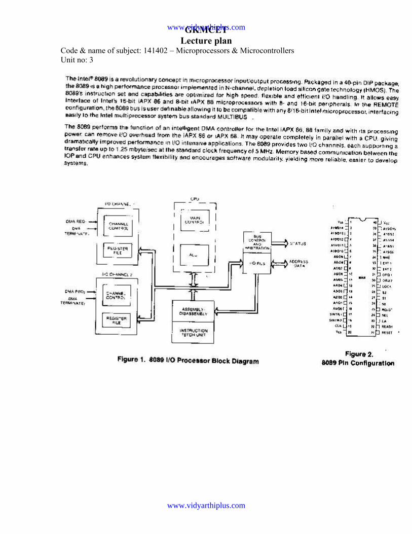
http:/
/csetu
be.co
.nr/
GKMCETLecture plan
Code & name of subject: 141402 – Microprocessors & MicrocontrollersUnit no: 3
www.vidyarthiplus.com
www.vidyarthiplus.com

http:/
/csetu
be.co
.nr/
GKMCETLecture plan
Code & name of subject: 141402 – Microprocessors & MicrocontrollersUnit no: 3
www.vidyarthiplus.com
www.vidyarthiplus.com

http:/
/csetu
be.co
.nr/
GKMCETLecture plan
Code & name of subject: 141402 – Microprocessors & MicrocontrollersUnit no: 3
www.vidyarthiplus.com
www.vidyarthiplus.com
GKMCETLecture plan
Code & name of subject: 141402 – Microprocessors & MicrocontrollersUnit no: 3
www.vidyarthiplus.com
www.vidyarthiplus.com

http:/
/csetu
be.co
.nr/
GKMCETLecture plan
Code & name of subject: 141402 – Microprocessors & MicrocontrollersUnit no: 3
www.vidyarthiplus.com
www.vidyarthiplus.com

http:/
/csetu
be.co
.nr/
GKMCETLecture plan
Code & name of subject: 141402 – Microprocessors & MicrocontrollersUnit no: 3
Communication between CPU and IOP:
The communication between CPU and IOP may take different forms depending on theparticular computer considered. The sequence of operations during CPU and IOPcommunication is shown in figure.
www.vidyarthiplus.com
www.vidyarthiplus.com

http:/
/csetu
be.co
.nr/
GKMCETLecture plan
Code & name of subject: 141402 – Microprocessors & MicrocontrollersUnit no: 3
The CPU sends a test I/O instruction to IOP to test the IOP path. The responds by inserting a status word in memory location. The CPU refers to the status word in memory. If everything is in order, the CPU
sends the start I/O instruction to start the I/O transfer. The IOP accesses memory for IOP program. The CPU can now continue with another program while the IOP is busy with the
program. Both programs refer to memory by means of DMA transfer.
www.vidyarthiplus.com
www.vidyarthiplus.com
GKMCETLecture plan
Code & name of subject: 141402 – Microprocessors & MicrocontrollersUnit no: 3
When the IOP terminates the execution of its program, it sends an interruptrequest to the CPU.
The CPU then issues a read I/O instruction to read the status from the IOP. The IOP transfers the status word to memory location. The status word indicates whether the transfer has been completed satisfactorily
or if any error has occurred during the transfer.
www.vidyarthiplus.com
www.vidyarthiplus.com

GKMCETLecture plan
Code & name of subject: 141402 – Microprocessors & MicrocontrollersUnit no: 4
UNIT-IV
I/O INTERFACING 9Memory interfacing and I/O interfacing with 8085–parallel communication interface–serial communicationinterface–timer-keyboard/display controller– interrupt controller–DMA controller (8237)–applications–steppermotor– temperature control..
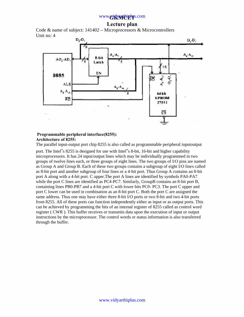
Memory InterfacingThe memory is made up of semiconductor material used to store the programs and data.Three types of memory is, Process memory Primary or main memory Secondary memory
Typical EPROM and Static RAMA typical semiconductor memory IC will have n address pins, m data pins (or output
pins).Having two power supply pins (one for connecting required supply voltage (V and theother for connecting ground).The control signals needed for static RAM are chip select (chip enable), read control(output enable) and write control (write enable).The control signals needed for read operation in EPROM are chip select (chip enable)
and read control (output enable).
DecoderIt is used to select the memory chip of processor during the execution of a program. Noof IC's used for decoder is, 2-4 decoder (74LS139) 3-8 decoder (74LS138)
www.vidyarthiplus.com
www.vidyarthiplus.com

GKMCETLecture plan
Code & name of subject: 141402 – Microprocessors & MicrocontrollersUnit no: 4
Number of Address Pins and Data Pins in Memory ICs
Example for Memory Interfacing
Consider a system in which the full memory space 64kb is utilized for EPROM memory.Interface the EPROM with 8085 processor.The memory capacity is 64 Kbytes. i.e
2^n = 64 x 1000 bytes where n = address lines. So, n = 16. In this system the entire 16 address lines of the processor are connected to address inputpins of memory IC in order to address the internal locations of memory. The chip select (CS) pin of EPROM is permanently tied to logic low (i.e., tied to ground). Since the processor is connected to EPROM, the active low RD pin is connected to activelow output enable pin of EPROM. The range of address for EPROM is 0000H to FFFFH.
www.vidyarthiplus.com
www.vidyarthiplus.com
GKMCETLecture plan
Code & name of subject: 141402 – Microprocessors & MicrocontrollersUnit no: 4
Programmable peripheral interface(8255):Architecture of 8255:The parallel input-output port chip 8255 is also called as programmable peripheral inputoutputport. The Intel‟s 8255 is designed for use with Intel‟s 8-bit, 16-bit and higher capabilitymicroprocessors. It has 24 input/output lines which may be individually programmed in twogroups of twelve lines each, or three groups of eight lines. The two groups of I/O pins are namedas Group A and Group B. Each of these two groups contains a subgroup of eight I/O lines calledas 8-bit port and another subgroup of four lines or a 4-bit port. Thus Group A contains an 8-bitport A along with a 4-bit port. C upper.The port A lines are identified by symbols PA0-PA7while the port C lines are identified as PC4-PC7. Similarly, GroupB contains an 8-bit port B,containing lines PB0-PB7 and a 4-bit port C with lower bits PC0- PC3. The port C upper andport C lower can be used in combination as an 8-bit port C. Both the port C are assigned thesame address. Thus one may have either three 8-bit I/O ports or two 8-bit and two 4-bit portsfrom 8255. All of these ports can function independently either as input or as output ports. Thiscan be achieved by programming the bits of an internal register of 8255 called as control wordregister ( CWR ). This buffer receives or transmits data upon the execution of input or outputinstructions by the microprocessor. The control words or status information is also transferredthrough the buffer.
www.vidyarthiplus.com
www.vidyarthiplus.com

GKMCETLecture plan
Code & name of subject: 141402 – Microprocessors & MicrocontrollersUnit no: 4
The signal description of 8255 are briefly presented as follows :
PA7-PA0: These are eight port A lines that acts as either latched output or buffered input linesdepending upon the control word loaded into the control word register.
PC7-PC4 : Upper nibble of port C lines. They may act as either output latches or input bufferslines.This port also can be used for generation of handshake lines in mode 1 or mode 2.
www.vidyarthiplus.com
www.vidyarthiplus.com

GKMCETLecture plan
Code & name of subject: 141402 – Microprocessors & MicrocontrollersUnit no: 4
PC3-PC0 : These are the lower port C lines, other details are the same as PC7-PC4 lines.
PB0-PB7 : These are the eight port B lines which are used as latched output lines or bufferedinput lines in the same way as port A.
RD : This is the input line driven by the microprocessor and should be low to indicate readoperation to 8255.
WR : This is an input line driven by the microprocessor. A low on this line indicates writeoperation.
CS : This is a chip select line. If this line goes low, it enables the 8255 to respond to RD and WRsignals, otherwise RD and WR signal are neglected.
A1-A0 : These are the address input lines and are driven by the microprocessor. These linesA1-A0 with RD, WR and CS from the following operations for 8255. These addresslines are used for addressing any one of the four registers,i.e. three ports and a control wordregister as given in table below. In case of 8086 systems, if the 8255 is to be interfaced with lower order data bus, the A0 andA1 pins of 8255 are connected with A1 and A2 respectively.
D0-D7 : These are the data bus lines those carry data or control word to/from themicroprocessor.
RESET : A logic high on this line clears the control word register of 8255. All ports are set asinput ports by default after reset.
Operational Modes of 8255There are two main operational modes of 8255:
1. Input/output mode 2. Bit set/reset mode
Input/Output ModeThere are three types of the input/output mode. They are as follows: Mode 0In this mode, the ports can be used for simple input/output operations without handshaking. Ifboth port A and B are initialized in mode 0, the two halves of port C can be either used togetheras an additional 8-bit port, or they can be used as individual 4-bit ports. Since the two halves ofport C are independent, they may be used such that one-half is initialized as an input port whilethe other half is initialized as an output port. The input output features in mode 0 are as follows:1. O/p are latched. 2. I/p are buffered not latched. 3. Port do not have handshake or interruptcapability.
Mode 1When we wish to use port A or port B for handshake (strobed) input or output operation, weinitialise that port in mode 1 (port A and port B can be initilalised to operate in differentmodes,ie, for eg, port A can operate in mode 0 and port B in mode 1). Some of the pins of port Cfunction as handshake lines.
www.vidyarthiplus.com
www.vidyarthiplus.com

GKMCETLecture plan
Code & name of subject: 141402 – Microprocessors & MicrocontrollersUnit no: 4For port B in this mode (irrespective of whether is acting as an input port or output port), PC0,PC1 and PC2 pins function as handshake lines.If port A is initialised as mode 1 input port, then, PC3, PC4 and PC5 function as handshakesignals. Pins PC6 and PC7 are available for use as input/output lines.The mode 1 which supports handshaking has following features: 1. Two ports i.e. port A and Bcan be use as 8-bit i/o port. 2. Each port uses three lines of port c as handshake signal andremaining two signals can be function as i/o port. 3. interrupt logic is supported. 4. Input andOutput data are latched.
Mode 2Only group A can be initialised in this mode. Port A can be used for bidirectional handshake datatransfer. This means that data can be input or output on the same eight lines (PA0 - PA7). PinsPC3 - PC7 are used as handshake lines for port A. The remaining pins of port C (PC0 - PC2) canbe used as input/output lines if group B is initialised in mode 0. In this mode, the 8255 may beused to extend the system bus to a slave microprocessor or to transfer data bytes to and from afloppy disk controller.
Bit Set/Reset (BSR) modeIn this mode only port b can be used (as an output port). Each line of port C (PC0 - PC7) can beset/reset by suitably loading the command word register.no effect occurs in input-output mode.The individual bits of port c can be set or reset by sending the signal OUT instruction to thecontrol register.
Control Word FormatInput/output mode format
Control Word format in input/output mode The figure shows the control word format in the input/output mode. This mode is selectedby making D7 = '1' . D0, D1, D3, D4 are for lower port C, port B, upper port C and port A respectively. WhenD0 or D1 or D3 or D4 are "SET", the corresponding ports act as input ports. For eg, if D0= D4 = '1', then lower port C and port A act as input ports. If these bits are "RESET",then the corresponding ports act as output ports. For eg, if D1 = D3 = '0', then port B andupper port C act as output ports. D2 is used for mode selection for group B (Port B and Lower Port C). When D2 = '0',mode 0 is selected and when D2 = '1', mode 1 is selected. D5, D6 are used for mode selection for group A (Upper Port C and Port A). The format isas follows:D6 D5 mode0 0 00 1 11 x 2
BSR mode format
www.vidyarthiplus.com
www.vidyarthiplus.com

http:/
/csetu
be.co
.nr/
GKMCETLecture plan
Code & name of subject: 141402 – Microprocessors & MicrocontrollersUnit no: 4
Control Word format in BSR mode
The figure shows the control word format in BSR mode. This mode is selected by makingD7='0'. D0 is used for bit set/reset. When D0= '1', the port C bit selected (selection of a port C bitis shown in the next point) is SET, when D0 = '0', the port C bit is RESET. D1, D2, D3 are used to select a particular port C bit whose value may be altered using D0bit as mentioned above. The selection of the port C bits are done as follows:
www.vidyarthiplus.com
www.vidyarthiplus.com

GKMCETLecture plan
Code & name of subject: 141402 – Microprocessors & MicrocontrollersUnit no: 4
D4, D5, D6 are not used.
Programmable Interrupt Controller(8259)Features 8 levels of interrupts. Can be cascaded in master-slave configuration to handle 64 levels of interrupts. Internal priority resolver. Fixed priority mode and rotating priority mode. Individually maskable interrupts. Modes and masks can be changed dynamically. Accepts IRQ, determines priority, checks whether incoming priority > current level
being serviced, issues interrupt signal. In 8085 mode, provides 3 byte CALL instruction. In 8086 mode, provides 8 bit vector number. Polled and vectored mode. Starting address of ISR or vector number is programmable. No clock required.
Pinout
www.vidyarthiplus.com
www.vidyarthiplus.com

http:/
/csetu
be.co
.nr/
GKMCETLecture plan
Code & name of subject: 141402 – Microprocessors & MicrocontrollersUnit no: 4
Block diagram
www.vidyarthiplus.com
www.vidyarthiplus.com
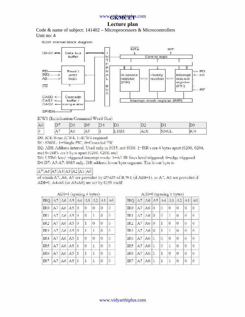
http:/
/csetu
be.co
.nr/
GKMCETLecture plan
Code & name of subject: 141402 – Microprocessors & MicrocontrollersUnit no: 4
www.vidyarthiplus.com
www.vidyarthiplus.com

http:/
/csetu
be.co
.nr/
GKMCETLecture plan
Code & name of subject: 141402 – Microprocessors & MicrocontrollersUnit no: 4
www.vidyarthiplus.com
www.vidyarthiplus.com

GKMCETLecture plan
Code & name of subject: 141402 – Microprocessors & MicrocontrollersUnit no: 4
UNIVERSAL SYNCHRONOUS ASYNCHRONOUS RECEIVERTRANSMITTER (USART)The 8251 is a USART (Universal Synchronous Asynchronous Receiver Transmitter) forserial data communication. As a peripheral device of a microcomputer system, the 8251receivesparallel data from the CPU and transmits serial data after conversion. This device also receivesserial data from the outside and transmits parallel data to the CPU after conversion.
Block Diagram of 8251
www.vidyarthiplus.com
www.vidyarthiplus.com

http:/
/csetu
be.co
.nr/
GKMCETLecture plan
Code & name of subject: 141402 – Microprocessors & MicrocontrollersUnit no: 4
Control WordsThere are two types of control word.1. Mode instruction (setting of function)2. Command (setting of operation)
1) Mode InstructionMode instruction is used for setting the function of the 8251. Mode instruction will be in "waitfor write" at either internal reset or external reset. That is, the writing of a control word afterresetting will be recognized as a "mode instruction."
Items set by mode instruction are as follows: Synchronous/asynchronous mode Stop bit length (asynchronous mode)
www.vidyarthiplus.com
www.vidyarthiplus.com
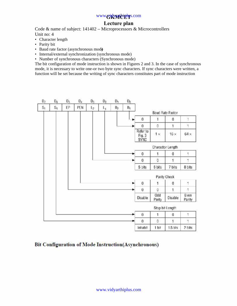
http:/
/csetu
be.co
.nr/
GKMCETLecture plan
Code & name of subject: 141402 – Microprocessors & MicrocontrollersUnit no: 4 Character length Parity bit Baud rate factor (asynchronous mode) Internal/external synchronization (synchronous mode) Number of synchronous characters (Synchronous mode)The bit configuration of mode instruction is shown in Figures 2 and 3. In the case of synchronousmode, it is necessary to write one-or two byte sync characters. If sync characters were written, afunction will be set because the writing of sync characters constitutes part of mode instruction
www.vidyarthiplus.com
www.vidyarthiplus.com

http:/
/csetu
be.co
.nr/
GKMCETLecture plan
Code & name of subject: 141402 – Microprocessors & MicrocontrollersUnit no: 4
2) CommandCommand is used for setting the operation of the 8251. It is possible to write a commandwhenever necessary after writing a mode instruction and sync characters.
Items to be set by command are as follows: Transmit Enable/Disable Receive Enable/Disable DTR, RTS Output of data. Resetting of error flag. Sending to break characters Internal resetting Hunt mode (synchronous mode)
www.vidyarthiplus.com
www.vidyarthiplus.com

http:/
/csetu
be.co
.nr/
GKMCETLecture plan
Code & name of subject: 141402 – Microprocessors & MicrocontrollersUnit no: 4
www.vidyarthiplus.com
www.vidyarthiplus.com

http:/
/csetu
be.co
.nr/
GKMCETLecture plan
Code & name of subject: 141402 – Microprocessors & MicrocontrollersUnit no: 4
Programmable Keyboard/Display Interface – 8279A programmable keyboard and display interfacing chip.Scans and encodes up to a 64-
key keyboard.Controls up to a 16-digit numerical display.Keyboard section has a built-in FIFO 8character buffer.The display is controlled from an internal 16x8 RAM tha stores the codeddisplay information.
www.vidyarthiplus.com
www.vidyarthiplus.com

GKMCETLecture plan
Code & name of subject: 141402 – Microprocessors & MicrocontrollersUnit no: 4
PINOUT:
A0: Selects data (0) or control/status (1) for reads and writes between micro and 8279. BD: Output that blanks the displays. CLK: Used internally for timing. Max is 3 MHz. CN/ST: Control/strobe, connected to the control key on the keyboard CS: Chip select that enables programming, reading the keyboard, etc. DB7-DB0: Consists of bidirectional pins that connect to data bus on micro. IRQ: Interrupt request, becomes 1 when a key is pressed, data is available. OUT A3-A0/B3-B0: Outputs that sends data to the most significant/least significant nibble of display. RD(WR): Connects to micro's IORC or RD signal, reads data/status registers. RESET: Connects to system RESET. RL7-RL0: Return lines are inputs used to sense key depression in the keyboard matrix. Shift: Shift connects to Shift key on keyboard. SL3-SL0: Scan line outputs scan both the keyboard and displays.
www.vidyarthiplus.com
www.vidyarthiplus.com
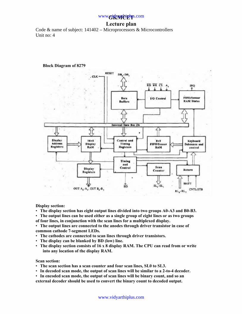
http:/
/csetu
be.co
.nr/
GKMCETLecture plan
Code & name of subject: 141402 – Microprocessors & MicrocontrollersUnit no: 4
Block Diagram of 8279
Display section: The display section has eight output lines divided into two groups A0-A3 and B0-B3. The output lines can be used either as a single group of eight lines or as two groupsof four lines, in conjunction with the scan lines for a multiplexed display. The output lines are connected to the anodes through driver transistor in case ofcommon cathode 7-segment LEDs. The cathodes are connected to scan lines through driver transistors. The display can be blanked by BD (low) line. The display section consists of 16 x 8 display RAM. The CPU can read from or write
into any location of the display RAM.
Scan section: The scan section has a scan counter and four scan lines, SL0 to SL3. In decoded scan mode, the output of scan lines will be similar to a 2-to-4 decoder. In encoded scan mode, the output of scan lines will be binary count, and so anexternal decoder should be used to convert the binary count to decoded output.
www.vidyarthiplus.com
www.vidyarthiplus.com

GKMCETLecture plan
Code & name of subject: 141402 – Microprocessors & MicrocontrollersUnit no: 4 The scan lines are common for keyboard and display. The scan lines are used to form the rows of a matrix keyboard and also connected to
digit drivers of a multiplexed display, to turn ON/OFF.
CPU interface section: The CPU interface section takes care of data transfer between 8279 and theprocessor. This section has eight bidirectional data lines DB0 to DB7 for data transfer between8279 and CPU. It requires two internal address A =0 for selecting data buffer and A = 1 forselecting control register of8279. The control signals WR (low), RD (low), CS (low) and A0 are used for read/write to8279. It has an interrupt request line IRQ, for interrupt driven data transfer withprocessor. The 8279 require an internal clock frequency of 100 kHz. This can be obtained bydividing the input clock by an internal prescaler. The RESET signal sets the 8279 in 16-character display with two -key lockout
keyboard modes.
DMA CONTROLLER 8237:
www.vidyarthiplus.com
www.vidyarthiplus.com

GKMCETLecture plan
Code & name of subject: 141402 – Microprocessors & MicrocontrollersUnit no: 4
www.vidyarthiplus.com
www.vidyarthiplus.com

http:/
/csetu
be.co
.nr/
GKMCETLecture plan
Code & name of subject: 141402 – Microprocessors & MicrocontrollersUnit no: 4
www.vidyarthiplus.com
www.vidyarthiplus.com

http:/
/csetu
be.co
.nr/
GKMCETLecture plan
Code & name of subject: 141402 – Microprocessors & MicrocontrollersUnit no: 4
www.vidyarthiplus.com
www.vidyarthiplus.com

GKMCETLecture plan
Code & name of subject: 141402 – Microprocessors & MicrocontrollersUnit no: 4
www.vidyarthiplus.com
www.vidyarthiplus.com
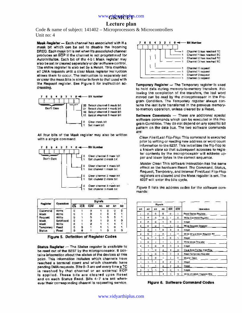
http:/
/csetu
be.co
.nr/
GKMCETLecture plan
Code & name of subject: 141402 – Microprocessors & MicrocontrollersUnit no: 4
www.vidyarthiplus.com
www.vidyarthiplus.com

GKMCETLecture plan
Code & name of subject: 141402 – Microprocessors & MicrocontrollersUnit no: 4
Interfacing I/O devices with 8085Techniques for I/O Interfacing:1.Peripheral-mapped I/O
2.Memory-mapped I/O
Memory-mapped I/O 8085 uses its 16-bit address bus to identify a memory location Memory address space: 0000H to FFFFH 8085 needs to identify I/O devices also I/O devices can be interfaced using addresses from memory space 8085 treats such an I/O device as a memory location This is called Memory-mapped I/O
Peripheral-mapped I/O 8085 has a separate 8-bit addressing scheme for I/O devices I/O address space: 00H to FFH This is called Peripheral-mapped I/O or I/O-mapped I/O
8085 Communication with I/O devices Involves the following three steps
1. Identify the I/O device (with address)2. Generate Timing & Control signals3. Data transfer takes place
8085 communicates with a I/O device only if there is a Program Instruction to do so
Identify the I/O device (with address)1. Memory-mapped I/O (16-bit address)
www.vidyarthiplus.com
www.vidyarthiplus.com

GKMCETLecture plan
Code & name of subject: 141402 – Microprocessors & MicrocontrollersUnit no: 4
2. Peripheral-mapped I/O (8-bit address)
Timing & Control Signals:Memory-mapped I/O
Reading Input: IO/M = 0, RD = 0 Write to Output: IO/M = 0, WR = 0
Peripheral-mapped I/O Reading Input: IO/M = 1, RD = 0 Write to Output: IO/M = 1, WR = 0
8085 Communication with I/O devices Involves the following three steps
Identify the I/O device (with address) Generate Timing & Control signals Data transfer takes place
8085 communicates with a I/O device only if there is a Program Instruction to do so
Peripheral I/O Instructions IN Instruction
Inputs data from input device into the accumulator It is a 2-byte instruction Format: IN 8-bit port address Example: IN 01H
OUT Instruction Outputs the contents of accumulator to an output device It is a 2-byte instruction Format: OUT 8-bit port address Example: OUT 02H
Memory-mapped I/O Instructions I/O devices are identified by 16-bit addresses 8085 communicates with an I/O device as if it were one of the memory locations Memory related instructions are used
For e.g. LDA, STALDA 8000H
Loads A with data read from input device with 16-bit address 8000HSTA 8001H
Stores (Outputs) contents of A to output device with 16-bit address8001H
Applications:
Stepper Motor:
The hardware setup consists of a microprocessor motherboard and stepper motorinterface board. The motherboard consists of 8085 MPU, 8KB EPROM, 8KB RAM, Keyboardand display controller 8279, 21-key Hex-keypad and six numbers of seven segment LEDs and
www.vidyarthiplus.com
www.vidyarthiplus.com

GKMCETLecture plan
Code & name of subject: 141402 – Microprocessors & MicrocontrollersUnit no: 4Bus Expansion connector. The stepper motor interface consists of driver transistors for steppermotor windings and address decoding circuit. The microprocessor output the binary sequencethrough data bus, which are converted to current pulses by the driver transistors and used to drivestepper motor. The software for the system is developed in 8085 assembly language.
Temperature Control:The temperature controller can be used to control the temperature of any plant. Typically it
contains a Processor unit, Temperature input unit and Control output unit. The 8085 basedmotherboard forms the processing unit. The Analog-to-Digital unit together with temperaturesensor forms the temperature input unit. The relay driver forms the control output unit. Electricpower to the heating element (coil) is supplied through relay contacts. The switching ON/OFF ofthe relay controls the heat supplied to the plant.
Fig1. Block diagram of stepper motor interface
EPROM8KB
8085CPU
LATCH
50 P
in E
xpan
sion
Con
nect
or
System bus
RAM8KB
8279KeyboardDisplay
D0-D
7
A0-A
7
Keyboard
AD0-AD7
Address/Control
Address/Decoder
Latches
BufferLED indication for
output binary sequence
D0-D3
Con
nect
or
M
Stepper driver
Transistor driver
Display
CS
C D E F int8 9 A B Go4 5 6 7 Nxt0 1 2 3 Sub
www.vidyarthiplus.com
www.vidyarthiplus.com

GKMCETLecture plan
Code & name of subject: 141402 – Microprocessors & MicrocontrollersUnit no: 4
TempInput
MPU Control output Plant
Simple schematic of temperature controller
Operationally, the system requires two set points-upper and lower, to be entered by theuser. Whenever the temperature of the plant exceeds the upper limit or recede the lower limitrelay is turned-off, so that a temperature is maintained within limits. The software for thetemperature controller is developed in 8085 assembly language programs.
The hardware consists of 8085 microprocessor motherboard, ADC interface board, andrelay anddriver unit.
The motherboard consists of 8085 MPU, 8KB EPROM, 8KB RAM keyboard and displaycontroller 8279, programmable peripheral interface 8255, 21 key hex-keypad and six numbers ofseven segment LED’s. Ports Expansion connector parallel port connectors are provided forexternal interfacing.
The temperature input board or ADC interface board consists of ADC 0809, which is an8-bit converter with eight channels of input. It is interfaced with the motherboard through 50-pinbus expansion connector. The temperature sensor ADC590 is used to sense the temperature ofthe plant and its analog output is applied to the channel-0 of ADC.
Relay is switched ON/OFF by driving the transistor to saturation/cut-off which isconnected to port A of 8255.
Fig 1. Simple schematic of temperature controller
www.vidyarthiplus.com
www.vidyarthiplus.com

GKMCETLecture plan
Code & name of subject: 141402 – Microprocessors & MicrocontrollersUnit no: 4
driver
8255 PPI
8085CPU
LATCH
ADCINTERFACE BOARD
SYSTEM BUS
EPROM 8KB
RAM8KB
8279KEYBOARD DISPLAY
AD590
TEMPERATURE SENSOR
DISPLAY
P
NC
C D E F
0 1 2 3
54 6 7
8 9 A B
int
Nxt
Sub
KEYBOARD
+V
50pi
nEx
pans
ion
conn
ecto
r
D-D 0
7
Para
llelp
ort
26pi
nco
nnec
tor
A-A 8
1 5
www.vidyarthiplus.com
www.vidyarthiplus.com

http:/
/csetu
be.co
.nr/
GKMCETLecture plan
Code & name of subject: 141402 – Microprocessors & MicrocontrollersUnit no: 5
UNIT VMICROCONTROLLERS 9Architecture of 8051 Microcontroller–signals– I/O ports–memory–counters andtimers – serial data I/O –
interrupts-Interfacing-keyboard, LCD,ADC & DAC
8051 MICROCONTROLLER• It is a single chip• Consists of Cpu, Memory• I/O ports, timers and other peripherals
www.vidyarthiplus.com
www.vidyarthiplus.com

http:/
/csetu
be.co
.nr/
GKMCETLecture plan
Code & name of subject: 141402 – Microprocessors & MicrocontrollersUnit no: 5
Memory Organization- Logical separation of program and data memory-Separate address spaces for Program (ROM) and Data (RAM) Memory-Allow Data Memory to be accessed by 8-bit addresses quickly and manipulated by8-bit CPU
-Only be read, not written to-The address space is 16-bit, so maximum of 64K bytes-Up to 4K bytes can be on-chip (internal) of 8051 core-PSEN (Program Store Enable) is used for access to external Program Memory
-Includes 128 bytes of on-chip Data Memory which are more easily accessibledirectly by its instructions-There is also a number of Special Function Registers (SFRs)-Internal Data Memory contains four banks of eight registers and a special 32-byte long segment which is bit addressable by 8051 bit-instructions-External memory of maximum 64K bytes is accessible by “movx”
www.vidyarthiplus.com
www.vidyarthiplus.com

http:/
/csetu
be.co
.nr/
GKMCETLecture plan
Code & name of subject: 141402 – Microprocessors & MicrocontrollersUnit no: 5
Interrupt StructureThe 8051 provides 4 interrupt sources
Port Structure
latch, anoutput driver and an input buffer
accessingexternal memory
ress (which is timemultiplexed with thebyte being written or read)
ing bit in theport SFR.
www.vidyarthiplus.com
www.vidyarthiplus.com

GKMCETLecture plan
Code & name of subject: 141402 – Microprocessors & MicrocontrollersUnit no: 5
Timer/Counter-bit Timer/Counter registers
Instruction FormatAn instruction is a command to the microprocessor to perform a given task on a specified data.Each instruction has two parts: one is task to be performed, called the operation code (opcode),and the second is the data to be operated on, called the operand. The operand (or data) can bespecified in various ways. It may include 8-bit (or 16-bit ) data, an internal register, a memorylocation, or 8-bit (or 16-bit) address. In some instructions, the operand is implicit.
Instruction word sizeThe 8051 instruction set is classified into the following three groups according to word size:1. One-word or 1-byte instructions2. Two-word or 2-byte instructions3. Three-word or 3-byte instructions
One-Byte InstructionsA 1-byte instruction includes the opcode and operand in the same byte. Operand(s) are internalregister and are coded into the instruction.These instructions are 1-byte instructions performingthree different tasks. In the first instruction, both operand registers are specified. In the secondinstruction, the operand B is specified and the accumulator is assumed. Similarly, in the thirdinstruction, the accumulator is assumed to be the implicit operand. These instructions are storedin 8-bit binary format in memory; each requires one memory location.
Two-Byte InstructionsIn a two-byte instruction, the first byte specifies the operation code and the second byte specifiesthe operand. Source operand is a data byte immediately following the opcode.
Three-Byte Instructions
www.vidyarthiplus.com
www.vidyarthiplus.com

GKMCETLecture plan
Code & name of subject: 141402 – Microprocessors & MicrocontrollersUnit no: 5In a three-byte instruction, the first byte specifies the opcode, and the following two bytes specifythe 16-bit address. Note that the second byte is the low-order address and the third byte is thehigh-order address.
Addressing Modes of 8051The 8051 provides a total of five distinct addressing modes.
(1) immediate(2) register(3) direct(4) register indirect(5) indexed
(1) Immediate Addressing Mode The operand comes immediately after the op-code. The immediate data must be preceded by the pound sign, "#".
(2) Register Addressing Mode Register addressing mode involves the use of registers to hold the data to bemanipulated.
(3)Direct Addressing Mode It is most often used to access RAM locations 30 - 7FH. This is due to the fact that register bank locations are accessed by the register names of R0 - R7. There is no such name for other RAM locations so must use direct addressing In the direct addressing mode, the data is in a RAM memory location whose address is known, and this address is given as a part of the instruction
www.vidyarthiplus.com
www.vidyarthiplus.com
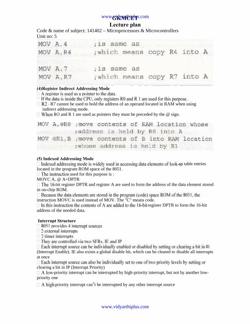
GKMCETLecture plan
Code & name of subject: 141402 – Microprocessors & MicrocontrollersUnit no: 5
(4)Register Indirect Addressing Mode
- R7 cannot be used to hold the address of an operand located in RAM when usingindirect addressing mode.
RO and R 1 are used as pointers they must be preceded by the @ sign.
(5) Indexed Addressing Mode-up table entries
located in the program ROM space of the 8051.n used for this purpose is :
MOVC A, @ A+DPTR-bit register DPTR and register A are used to form the address of the data element stored
in on-chip ROM.
instruction MOVC is used instead of MOV. The "C" means code.-bit register DPTR to form the 16-bit
address of the needed data.
Interrupt Structure
pts
in IE(Interrupt Enable). IE also exists a global disable bit, which can be cleared to disable all interruptsat once
orclearing a bit in IP (Interrupt Priority)
-priority interrupt can be interrupted by high-priority interrupt, but not by another low-priority one
-priority interrupt can‟t be interrupted by any other interrupt source
www.vidyarthiplus.com
www.vidyarthiplus.com

GKMCETLecture plan
Code & name of subject: 141402 – Microprocessors & MicrocontrollersUnit no: 5
pollingsequence determines which request is serviced, so within each priority lever there is a secondpriority structure
followingtable
External Interrupt
-activated-activated
-chip hardware clears that flag that generated an external interrupt when the serviceroutine is vectored to, but only if the interrupt was transition-activated
-activated, then the external requesting source is controllingthe request flag, not the on-chip hardware
Handling Interrupttly, when the flag for an enabled interrupt is found to be set
(1)), the interrupt system generates an LCALL to the appropriate location in Program Memory,unless some other conditions block the interrupt
terrupt of equal or higher priority level is already in progressin progress
flag is active but not being responded to for one of the above conditions, must bestill active when the blocking condition is removed, or the denied interrupt will not be serviced
-generated LCALL causes only thecontents of the Program Counter to be pushed onto the stack, and reloads the PC with thebeginning address of the service routine
it doesn‟t. Itclears an external interrupt flag (IE0 or IE1) only if it was transitionavtivated.
decide how muchtime to spend saving other registers. Programmer must also be more careful with proper selection,which register to save.
locations arespaced at 8-byte interval, beginning at 0003H for External Interrupt 0, 000BH for Timer 0, 0013Hfor External Interrupt 1 and 001BH for Timer 1.
www.vidyarthiplus.com
www.vidyarthiplus.com

GKMCETLecture plan
Code & name of subject: 141402 – Microprocessors & MicrocontrollersUnit no: 5
I/O Ports
anoutput driver and an input buffer
put buffer of Port 0 and output driver of Port 2 are used for accessingexternal memory
with thebyte being written or read)
rt 2 outputs the high byte (only needed when the address is 16 bits wide)
port SFR
TimersThe 8051 comes equipped with two timers, both of which may be controlled, set, read, andconfigured individually. The 8051 timers have three general functions: 1) Keeping time and/orcalculating the amount of time between events, 2) Counting the events themselves, or 3)Generating baud rates for the serial port.one of the primary uses of timers is to measure time. We will discuss this use of timers first andwill subsequently discuss the use of timers to count events. When a timer is used to measure timeit is also called an "interval timer" since it is measuring the time of the interval between twoevents.
www.vidyarthiplus.com
www.vidyarthiplus.com
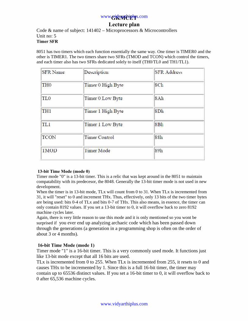
GKMCETLecture plan
Code & name of subject: 141402 – Microprocessors & MicrocontrollersUnit no: 5Timer SFR
8051 has two timers which each function essentially the same way. One timer is TIMER0 and theother is TIMER1. The two timers share two SFRs (TMOD and TCON) which control the timers,and each timer also has two SFRs dedicated solely to itself (TH0/TL0 and TH1/TL1).
13-bit Time Mode (mode 0)Timer mode "0" is a 13-bit timer. This is a relic that was kept around in the 8051 to maintaincompatability with its predecesor, the 8048. Generally the 13-bit timer mode is not used in newdevelopment.When the timer is in 13-bit mode, TLx will count from 0 to 31. When TLx is incremented from31, it will "reset" to 0 and increment THx. Thus, effectively, only 13 bits of the two timer bytesare being used: bits 0-4 of TLx and bits 0-7 of THx. This also means, in essence, the timer canonly contain 8192 values. If you set a 13-bit timer to 0, it will overflow back to zero 8192machine cycles later.Again, there is very little reason to use this mode and it is only mentioned so you wont besurprised if you ever end up analyzing archaeic code which has been passed downthrough the generations (a generation in a programming shop is often on the order ofabout 3 or 4 months).
16-bit Time Mode (mode 1)Timer mode "1" is a 16-bit timer. This is a very commonly used mode. It functions justlike 13-bit mode except that all 16 bits are used.TLx is incremented from 0 to 255. When TLx is incremented from 255, it resets to 0 andcauses THx to be incremented by 1. Since this is a full 16-bit timer, the timer maycontain up to 65536 distinct values. If you set a 16-bit timer to 0, it will overflow back to0 after 65,536 machine cycles.
www.vidyarthiplus.com
www.vidyarthiplus.com
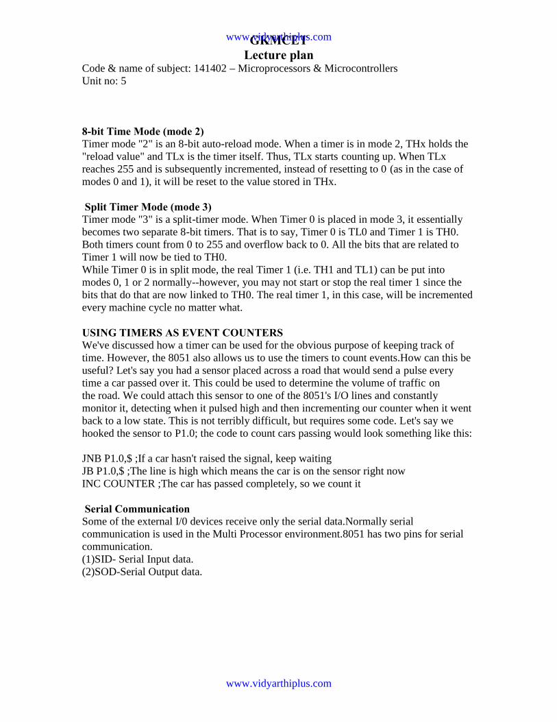
GKMCETLecture plan
Code & name of subject: 141402 – Microprocessors & MicrocontrollersUnit no: 5
8-bit Time Mode (mode 2)Timer mode "2" is an 8-bit auto-reload mode. When a timer is in mode 2, THx holds the"reload value" and TLx is the timer itself. Thus, TLx starts counting up. When TLxreaches 255 and is subsequently incremented, instead of resetting to 0 (as in the case ofmodes 0 and 1), it will be reset to the value stored in THx.
Split Timer Mode (mode 3)Timer mode "3" is a split-timer mode. When Timer 0 is placed in mode 3, it essentiallybecomes two separate 8-bit timers. That is to say, Timer 0 is TL0 and Timer 1 is TH0.Both timers count from 0 to 255 and overflow back to 0. All the bits that are related toTimer 1 will now be tied to TH0.While Timer 0 is in split mode, the real Timer 1 (i.e. TH1 and TL1) can be put intomodes 0, 1 or 2 normally--however, you may not start or stop the real timer 1 since thebits that do that are now linked to TH0. The real timer 1, in this case, will be incrementedevery machine cycle no matter what.
USING TIMERS AS EVENT COUNTERSWe've discussed how a timer can be used for the obvious purpose of keeping track oftime. However, the 8051 also allows us to use the timers to count events.How can this beuseful? Let's say you had a sensor placed across a road that would send a pulse everytime a car passed over it. This could be used to determine the volume of traffic onthe road. We could attach this sensor to one of the 8051's I/O lines and constantlymonitor it, detecting when it pulsed high and then incrementing our counter when it wentback to a low state. This is not terribly difficult, but requires some code. Let's say wehooked the sensor to P1.0; the code to count cars passing would look something like this:
JNB P1.0,$ ;If a car hasn't raised the signal, keep waitingJB P1.0,$ ;The line is high which means the car is on the sensor right nowINC COUNTER ;The car has passed completely, so we count it
Serial CommunicationSome of the external I/0 devices receive only the serial data.Normally serialcommunication is used in the Multi Processor environment.8051 has two pins for serialcommunication.(1)SID- Serial Input data.(2)SOD-Serial Output data.
www.vidyarthiplus.com
www.vidyarthiplus.com
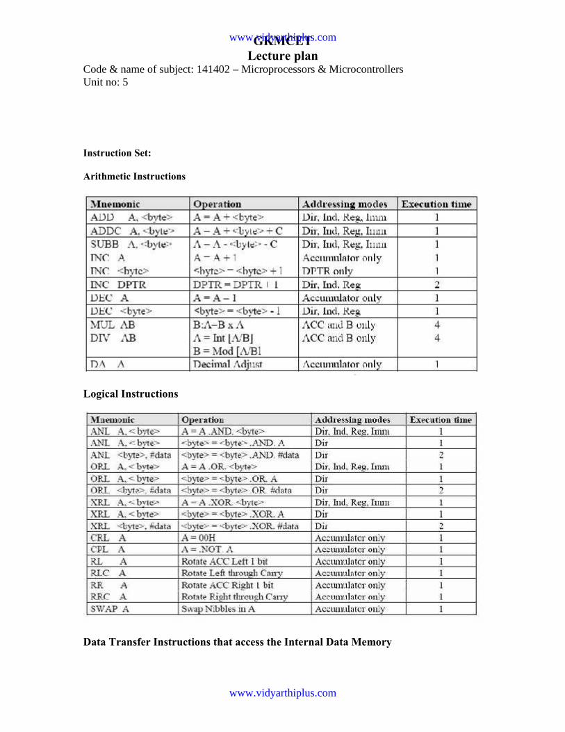
GKMCETLecture plan
Code & name of subject: 141402 – Microprocessors & MicrocontrollersUnit no: 5
Instruction Set:
Arithmetic Instructions
Logical Instructions
Data Transfer Instructions that access the Internal Data Memory
www.vidyarthiplus.com
www.vidyarthiplus.com
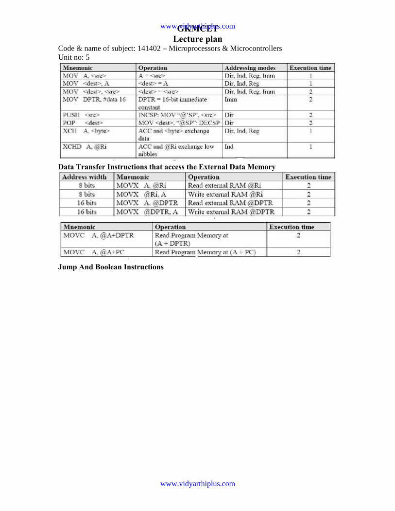
GKMCETLecture plan
Code & name of subject: 141402 – Microprocessors & MicrocontrollersUnit no: 5
Data Transfer Instructions that access the External Data Memory
Jump And Boolean Instructions
www.vidyarthiplus.com
www.vidyarthiplus.com

GKMCETLecture plan
Code & name of subject: 141402 – Microprocessors & MicrocontrollersUnit no: 5
Interfacing Keyboard to 8051 MicrocontrollerThe key board here we are interfacing is a matrix keyboard. This key board is designed with aparticular rows and columns. These rows and columns are connected to the microcontrollerthrough its ports of the micro controller 8051. We normally use 8*8 matrix key board. So onlytwo ports of 8051 can be easily connected to the rows and columns of the key board.When ever a key is pressed, a row and a column gets shorted through that pressed key and all theother keys are left open. When a key is pressed only a bit in the port goes high. Which indicatesmicrocontroller that the key is pressed. By this high on the bit key in the corresponding column isidentified.Once we are sure that one of key in the key board is pressed next our aim is to identify that key.To do this we firstly check for particular row and then we check the corresponding column thekey board.To check the row of the pressed key in the keyboard, one of the row is made high by making oneof bit in the output port of 8051 high . This is done until the row is found out. Once we get therow next out job is to find out the column of the pressed key. The column is detected by contentsin the input ports with the help of a counter. The content of the input port is rotated with carryuntil the carry bit is set.The contents of the counter is then compared and displayed in the display. This display isdesigned using a seven segment display and a BCD to seven segment decoder IC 7447. The BCDequivalent number of counter is sent through output part of 8051 displays the number of pressedkey.
Interfacing Keyboard to 8051 Microcontroller
www.vidyarthiplus.com
www.vidyarthiplus.com

http:/
/csetu
be.co
.nr/
GKMCETLecture plan
Code & name of subject: 141402 – Microprocessors & MicrocontrollersUnit no: 5
Circuit Diagram of Interfacing Keyboard to8051
Program for Keyboard Interfacing with 8051
Start of main program:
to check that whether any key is pressedstart: mov a,#00hmov p1,a ;making all rows of port p1 zeromov a,#0fhmov p1,a ;making all rows of port p1 highpress: mov a,p2jz press ;check until any key is pressed
after making sure that any key is pressedmov a,#01h ;make one row high at a timemov r4,amov r3,#00h ;initiating counternext: mov a,r4mov p1,a ;making one row high at a timemov a,p2 ;taking input from port Ajnz colscan ;after getting the row jump to checkcolumnmov a,r4
www.vidyarthiplus.com
www.vidyarthiplus.com

GKMCETLecture plan
Code & name of subject: 141402 – Microprocessors & MicrocontrollersUnit no: 5rl a ;rotate left to check next rowmov r4,amov a,r3add a,#08h ;increment counter by 08 countmov r3,asjmp next ;jump to check next row
after identifying the row to check the colomn following steps are followecolscan: mov r5,#00hin: rrc a ;rotate right with carry until get the carryjc out ;jump on getting carryinc r3 ;increment one countjmp inout: mov a,r3da a ;decimal adjust the contents of counterbefore displaymov p2,ajmp start ;repeat for check next key.
Interfacing LCD to 8051:
Liquid Crystal Display also called as LCD is very helpful in providing userinterface as well as for debugging purpose. The most common type of LCD controller isHITACHI 44780 which provides a simple interface between the controller & an LCD.
These LCD's are very simple to interface with the controller as well as are costeffective.
The most commonly used ALPHANUMERICdisplays are
1x16 (Single Line & 16 characters),
2x16 (Double Line & 16 character per line),
4x20 (four lines & Twenty characters per line).
The LCD requires 3 control lines (RS, R/W & EN) & 8 (or 4) data lines. The number ondata lines depends on the mode of operation. If operated in 8-bit mode then 8 data lines +3 control lines i.e. total 11 lines are required. And if operated in 4-bit mode then 4 datalines + 3 control lines i.e. 7 lines are required. How do we decide which mode to use? It’ssimple if you have sufficient data lines you can go for 8 bit mode & if there is a timeconstrain i.e. display should be faster then we have to use 8-bit mode because basically 4-bit mode takes twice as more time as compared to 8-bit mode.
www.vidyarthiplus.com
www.vidyarthiplus.com

GKMCETLecture plan
Code & name of subject: 141402 – Microprocessors & MicrocontrollersUnit no: 5
Pin Symbol Function1 Vss Ground2 Vdd Supply Voltage3 Vo Contrast Setting4 RS Register Select5 R/W Read/Write Select6 En Chip Enable Signal7-14 DB0-DB7 Data Lines15 A/Vee Gnd for the backlight16 K Vcc for backlight
When RS is low (0), the data is to be treated as a command. When RS is high (1), the databeing sent is considered as text data which should be displayed on the screen.
When R/W is low (0), the information on the data bus is being written to the LCD. WhenRW is high (1), the program is effectively reading from the LCD. Most of the times thereis no need to read from the LCD so this line can directly be connected to Gnd thus savingone controller line.
The ENABLE pin is used to latch the data present on the data pins. A HIGH - LOWsignal is required to latch the data. The LCD interprets and executes our command at theinstant the EN line is brought low. If you never bring EN low, your instruction will neverbe executed.
www.vidyarthiplus.com
www.vidyarthiplus.com

GKMCETLecture plan
Code & name of subject: 141402 – Microprocessors & MicrocontrollersUnit no: 5For Contrast setting a 10K pot should be used as shown in the figure.
Display Data Ram (DDRAM) stores the display data. So when we have to display acharacter on LCD we basically write it into DDRAM. For a 2x16 LCD the DDRAMaddress for first line is from 80h to 8fh & for second line is 0c0h to 0cfh. So if we want todisplay 'H' on the 7th postion of the first line then we will write it at location 87h.
Now as you have noticed two types of data is given to the LCD data to be displayed,command or special instruction.So now let us write a subroutine for both the type of data
Data to be Displayed
lcd_datadisplay:
SETB RS //Telling the LCD that the data which is being send is tobe displayed
MOV P1,A //Character to be displayed is in AccSETB ENCLR EN //High to Low pulse on EN to latch the dataCALL DELAY //Delay so that LCD finishes its internal operationsret
Command or Special Instruction
lcd_command:
CLR RS //Telling the LCD that the data which is being send is acommand
MOV P1,A //Character to be displayed is in AccSETB ENCLR EN //High to Low pulse on EN to latch the dataCALL DELAY //Delay so that LCD finishes its internal operationsret
Here I have used delay at the end of both the subroutines this is done to wait until theinstruction is completely executed by the LCD. This will assure that our program givesthe LCD the time it needs to execute instructions and also makes our program compatiblewith any LCD, regardless of how fast or slow it is.
www.vidyarthiplus.com
www.vidyarthiplus.com

GKMCETLecture plan
Code & name of subject: 141402 – Microprocessors & MicrocontrollersUnit no: 5
"*" - Not Used/Ignored. This bit can be either "1" or "0"
Set Cursor Move Direction:
ID - Increment the Cursor After Each Byte Written to Display if Set
S - Shift Display when Byte Written to Display Enable Display/Cursor
D - Turn Display On(1)/Off(0) C - Turn Cursor On(1)/Off(0)
B - Cursor Blink On(1)/Off(0)
Set Cursor Move Direction:
ID - Increment the Cursor After Each Byte Written to Display if Set
S - Shift Display when Byte Written to Display Enable Display/Cursor
D - Turn Display On(1)/Off(0) C - Turn Cursor On(1)/Off(0)
B - Cursor Blink On(1)/Off(0)
Move Cursor/Shift Display
SC - Display Shift On(1)/Off(0) RL - Direction of Shift Right(1)/Left(0)
Set Interface Length
DL - Set Data Interface Length 8(1)/4(0)
N - Number of Display Lines 1(0)/2(1)
www.vidyarthiplus.com
www.vidyarthiplus.com

GKMCETLecture plan
Code & name of subject: 141402 – Microprocessors & MicrocontrollersUnit no: 5F - Character Font 5x10(1)/5x7(0)
Poll the "Busy Flag" BF - This bit is set while the LCD is processing
Move Cursor to CGRAM/Display
A - Address
Read/Write ASCII to the Display
D - Data
The above Table shows the different commands for the LCD. I wont go into its details.
Before starting to display on LCD we need to Initialize it. Firstly we must tell the LCDwhether we'll be using 8-bit or 4-bit mode. Also we will be telling the LCD that we need5x8 character font. Both these options are selected using a single command i.e. 38h. So toactivate both these options we must execute following instructions:
MOV A,#38h
CALL lcd_command
Now that we have to Turn On the display & set the cursor option i.e. cursor ON/OFF &Cursor blinking ON/OFF for that we will use the command 0Eh i.e. Display On , CursorON but Cursor blinking OFF.
MOV A,#0Eh
CALL lcd_command
And the last command we require is to configure the LCD in such a way that everytimewe send a character to it the cursor position automatically increments by one & moves toright i.e. 06h.
MOV A,#06h
CALL lcd_command
So the lcd_initialize contains the following instructions
www.vidyarthiplus.com
www.vidyarthiplus.com

GKMCETLecture plan
Code & name of subject: 141402 – Microprocessors & MicrocontrollersUnit no: 5lcd_initialize:
MOV A,#38h
CALL lcd_command
MOV A,#38h
CALL lcd_command
MOV A,#38h
CALL lcd_command
ret
Similarly another important instruction that we require is Clearing the LCD i.e.
lcd_clr:
MOV A,#01h
CALL lcd_command
ret
Now we know all the commands to display on LCD. Let us write a program that willdisplay 'DNA TECHNOLOGY' on LCD.
ORG 0000h CALL lcd_initialize CALL lcd_clr MOV A,#80h //Location from where Data is to be displayed CALL lcd_command MOV A,#'D' CALL lcd_datadisplay MOV A,#'N' CALL lcd_datadisplay MOV A,#'A' CALL lcd_datadisplay MOV A,#20h //Hex value for blank space to be displayed CALL lcd_datadisplay MOV A,#'T'
www.vidyarthiplus.com
www.vidyarthiplus.com

GKMCETLecture plan
Code & name of subject: 141402 – Microprocessors & MicrocontrollersUnit no: 5 CALL lcd_datadisplay MOV A,#'E' CALL lcd_datadisplay MOV A,#'C' CALL lcd_datadisplay MOV A,#'H' CALL lcd_datadisplay MOV A,#'N' CALL lcd_datadisplay MOV A,#'O' CALL lcd_datadisplay MOV A,#'L' CALL lcd_datadisplay MOV A,#'O' CALL lcd_datadisplay MOV A,#'G' CALL lcd_datadisplay MOV A,#'Y' CALL lcd_datadisplay stop: ajmp stop
Interfacing ADC0808 To 8051
In lot of embedded systems microcontrollers needs to take analog input. Most of thesensors & transducers such as temperature, humidity, pressure, are analog. Forinterfacing these sensors to microcontrollers we require to convert the analog output ofthese sensors to digital so that the controller can read it. Some microcontrollers have builtin Analog to Digital Convertor (ADC) so there is no need of external ADC. Formicrocontrollers that don’t have internal ADC external ADC is used.
One of the most commonly used ADC is ADC0808. ADC 0808 is a Successiveapproximation type with 8 channels i.e. it can directly access 8 single ended analogsignals.
I/O Pins
ADDRESS LINE A, B, C
The device contains 8-channels. A particular channel is selected by using the addressdecoder line. The TABLE 1 shows the input states for address lines to select any channel.
www.vidyarthiplus.com
www.vidyarthiplus.com
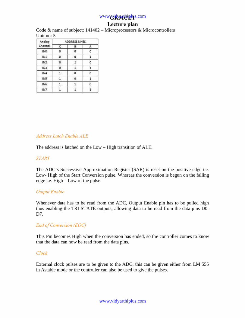
GKMCETLecture plan
Code & name of subject: 141402 – Microprocessors & MicrocontrollersUnit no: 5
Address Latch Enable ALE
The address is latched on the Low – High transition of ALE.
START
The ADC’s Successive Approximation Register (SAR) is reset on the positive edge i.e.Low- High of the Start Conversion pulse. Whereas the conversion is begun on the fallingedge i.e. High – Low of the pulse.
Output Enable
Whenever data has to be read from the ADC, Output Enable pin has to be pulled highthus enabling the TRI-STATE outputs, allowing data to be read from the data pins D0-D7.
End of Conversion (EOC)
This Pin becomes High when the conversion has ended, so the controller comes to knowthat the data can now be read from the data pins.
Clock
External clock pulses are to be given to the ADC; this can be given either from LM 555in Astable mode or the controller can also be used to give the pulses.
www.vidyarthiplus.com
www.vidyarthiplus.com
GKMCETLecture plan
Code & name of subject: 141402 – Microprocessors & MicrocontrollersUnit no: 5ALGORITHM 1. Start. 2. Select the channel. 3. A Low – High transition on ALEto latch in the address. 4. A Low – High transition on Start to reset the ADC’s SAR.5. A High – Low transition on ALE. 6. A High – Low transition on start to start theconversion. 7. Wait for End of cycle (EOC) pin to become high. 8. Make OutputEnable pin High. 9. Take Data from the ADC’s output 10. Make Output Enable pinLow. 11. Stop
The total numbers of lines required are:
datalines:8ALE:1START:1EOC:1Output Enable:1
I.e. total 12 lines. You can directly connect the OE pin to Vcc. Moreover instead ofpolling for EOC just put some delay so instead of 12 lines you will require 10 lines.
You can also provide the clock through the controller thus eliminating the need ofexternal circuit for clock.
Calculating Step Size
ADC 0808 is an 8 bit ADC i.e. it divides the voltage applied at Vref+ & Vref- into 28 i.e.256 steps.
Step Size = (Vref+ - Vref-)/256
Suppose Vref+ is connected to Vcc i.e. 5V & Vref- is connected to the Gnd then the stepsize will be
Step size= (5 - 0)/256= 19.53 mv.
Calculating Dout.
The data we get at the D0 - D7 depends upon the step size & the Input voltage i.e. Vin.
Dout = Vin /step Size.
If you want to interface sensors like LM35 which has output 10mv/°C then I wouldsuggest that you set the Vref+ to 2.56v so that the step size will be
Step size= (2.56 - 0)/256= 10 mv.
www.vidyarthiplus.com
www.vidyarthiplus.com
http:/
/csetu
be.co
.nr/
GKMCETLecture plan
Code & name of subject: 141402 – Microprocessors & MicrocontrollersUnit no: 5So now whatever reading that you get from the ADC will be equal to the actualtemperature.
PROGRAM
Here is a program for interfacing the ADC to microcontroller, as stated above I haveassumed that the OE pin is connected to Vcc & the clock is given by the controller.
This program selects channel 0 as input channel reads from it & saves in the accumulator.
adc_a bit p2.0
adc_b bit p2.1
adc_c bit p2.2
adc_start bit p2.3
adc_ale bit p2.4
adc_clk bit P2.5Org 0000h
clr ale
clr start
clr adc_a
clr adc_b ;Select Channel 0
clr adc_c
call delay_small
setb adc_ale ;ale pin high
call delay_small
setb adc_start ;start pin high
www.vidyarthiplus.com
www.vidyarthiplus.com
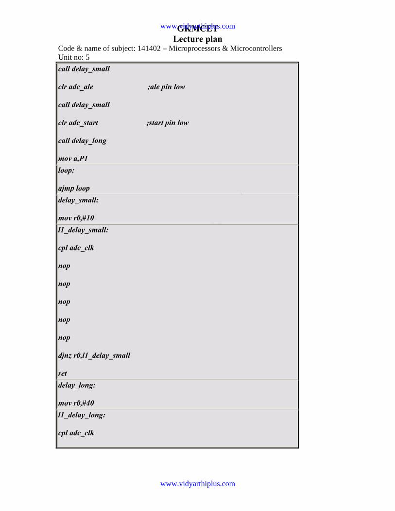
http:/
/csetu
be.co
.nr/
GKMCETLecture plan
Code & name of subject: 141402 – Microprocessors & MicrocontrollersUnit no: 5call delay_small
clr adc_ale ;ale pin low
call delay_small
clr adc_start ;start pin low
call delay_long
mov a,P1loop:
ajmp loopdelay_small:
mov r0,#10l1_delay_small:
cpl adc_clk
nop
nop
nop
nop
nop
djnz r0,l1_delay_small
retdelay_long:
mov r0,#40l1_delay_long:
cpl adc_clk
www.vidyarthiplus.com
www.vidyarthiplus.com

GKMCETLecture plan
Code & name of subject: 141402 – Microprocessors & MicrocontrollersUnit no: 5nop
nop
nop
nop
nop
djnz r0,l1_delay_long
retEnd
www.vidyarthiplus.com
www.vidyarthiplus.com