from atoms to bits - wireless | t/ict4d lab
TRANSCRIPT


Layout of the Lecture
Analog interfacing to sensors:
Signal conditioning Sampling and quantization Bridge circuits and instrumentation amplifiers
Linearization
Design for low power
Digital interfacing to sensors

Desirable Sensor Characteristics
Sensor reading equal to the measured quantity
Suitable
accuracy, precision, range, sensitivity → gain resolution, etc.
Low noise
Linearity

Characteristics of Instrumentation
Accuracy: How close is the measurement to measured.
Precision: What is the uncertainty in the measurement.
Range: Which value interval is measurable?
Sensitivity: For a given change in input, the amount of the change in output.
Resolution: Smallest amount of measurable change
Repeatability: Under the same conditions, can we get the same measurement?
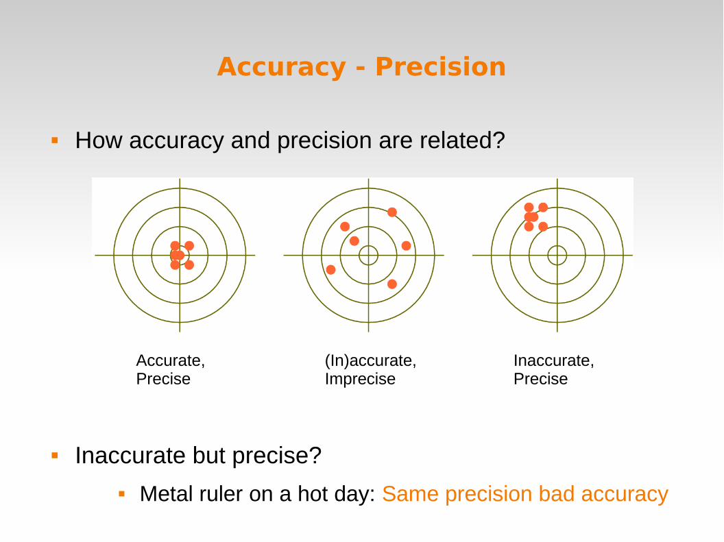
Accuracy - Precision
How accuracy and precision are related?
Inaccurate but precise?
Metal ruler on a hot day: Same precision bad accuracy
Accurate,Precise
(In)accurate,Imprecise
Inaccurate,Precise

Sensitivity - Range
Generally high sensitivity sounds good.
However, high sensitivity restricts range.
Deliberately→nonlinear sensor can be used.
1mV precision;
8bit: 0.256V range 12bit: 4.096V
High sensitivityLow sensitivityNonlinear

Analog Interfacing to Sensors
There are 3 main stages in sensing:
Physics
Electronics
Information
→Pysics will not be treated.

Signal Conditioning Electronics

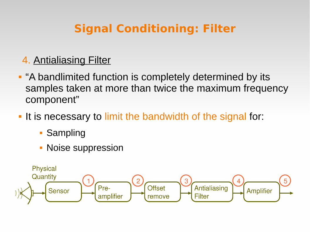
Signal Conditioning System
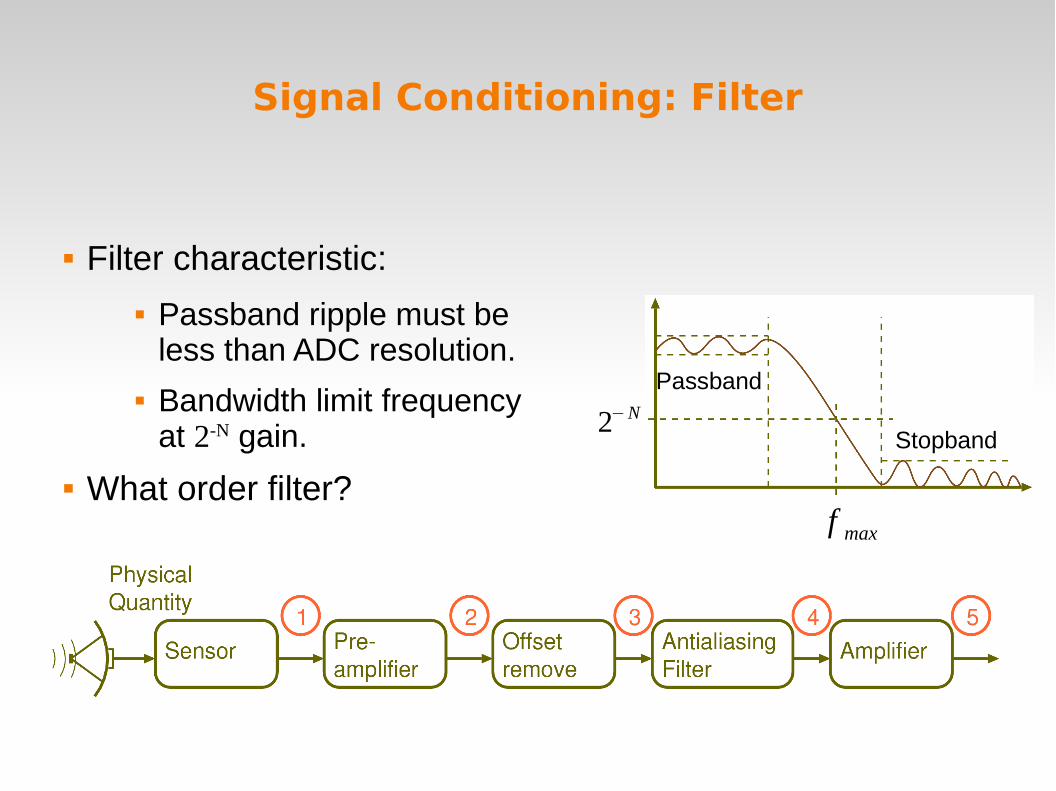
1. Sensor Output
2. Preamplifier stage
3. Removal of offset
4. Antialiasing filter
5. Amplifier
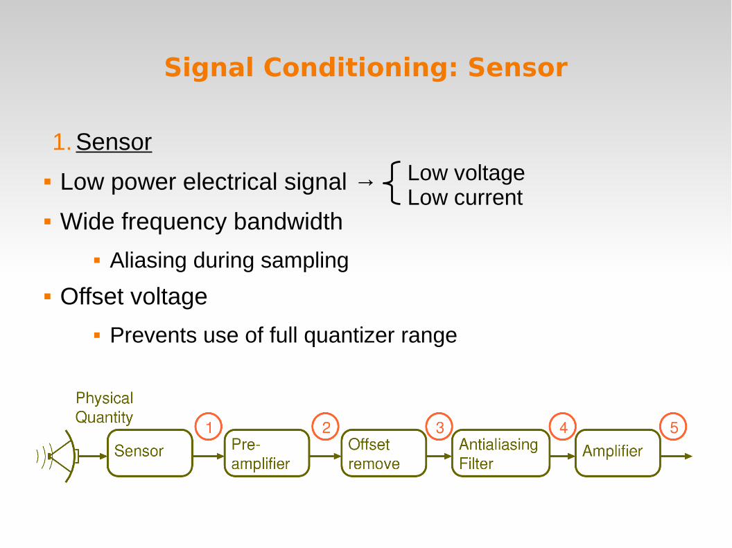
Signal Conditioning: Sensor
1. Sensor
Low power electrical signal →
Wide frequency bandwidth
Aliasing during sampling
Offset voltage
Prevents use of full quantizer range
Low voltageLow current

Signal Conditioning: Sensor
1. Sensor
Voltage source with impedance
OR
(Calculate like a voltage divider)ri=V s /ii
Po max→r o=ri
ri→∞ :V s=X s
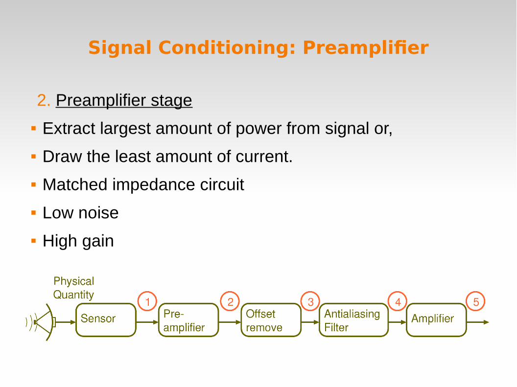
Signal Conditioning: Preamplifier
2. Preamplifier stage
Extract largest amount of power from signal or,
Draw the least amount of current.
Matched impedance circuit
Low noise
High gain

Signal Conditioning: Preamplifier
Draw the least amount of current:
Voltage follower configuration
Susceptibility to ESD increases.ri=2×10¹⁷Ω

Signal Conditioning: Offset Removal
3. Offset remove
The information content is confined toa small part of the signal range.
Amplification will not allowmax precision of the quantizer:2 MSB always set: 11xxxxxx12 bit ADC → 10bit ADC
Information content
No information
Xp
t
Xo
t

Signal Conditioning: Offset Removal
3. Offset remove
Difference amplifier.
Voff : Constant offset voltage for removal.
V o=Rf
R1
(V p−V off )
Signal Conditioning: Filter
4. Antialiasing Filter
“A bandlimited function is completely determined by its samples taken at more than twice the maximum frequency component”
It is necessary to limit the bandwidth of the signal for:
Sampling Noise suppression
Signal Conditioning: Filter
Filter characteristic:
Passband ripple must beless than ADC resolution.
Bandwidth limit frequencyat 2-N gain.
What order filter?
Passband
Stopband2−N
f max

Signal Conditioning: Amplifier
5. Amplification
Signal is amplified to the reference voltage of the ADC.
t
Xa
xa(t )<xmax=V ref
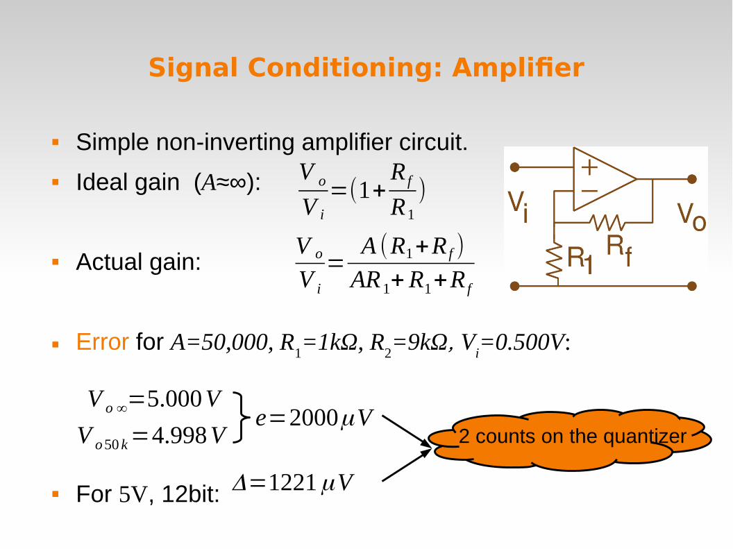
Signal Conditioning: Amplifier
Simple non-inverting amplifier circuit.
Ideal gain (A≈∞):
Actual gain:
Error for A=50,000, R1=1kΩ, R
2=9kΩ, V
i=0.500V:
For 5V, 12bit:
V o
V i
=(1+R f
R1
)
V o
V i
=A (R1+R f )
AR 1+ R1+R f
V o ∞=5.000 V
V o 50 k=4.998 V
Δ=1221μV
e=2000μV2 counts on the quantizer

Data Converter
6. Sample and Hold
7. Quantizer

Sample and Hold
Ideal sampling requires
zero duration and infinite currents.
Actual sampling uses a transistor…
The body resistance of the transistorturns the S&H into a low pass filter.
Ideal sample and hold
Actual sample and hold
Sample and hold equivalent circuit
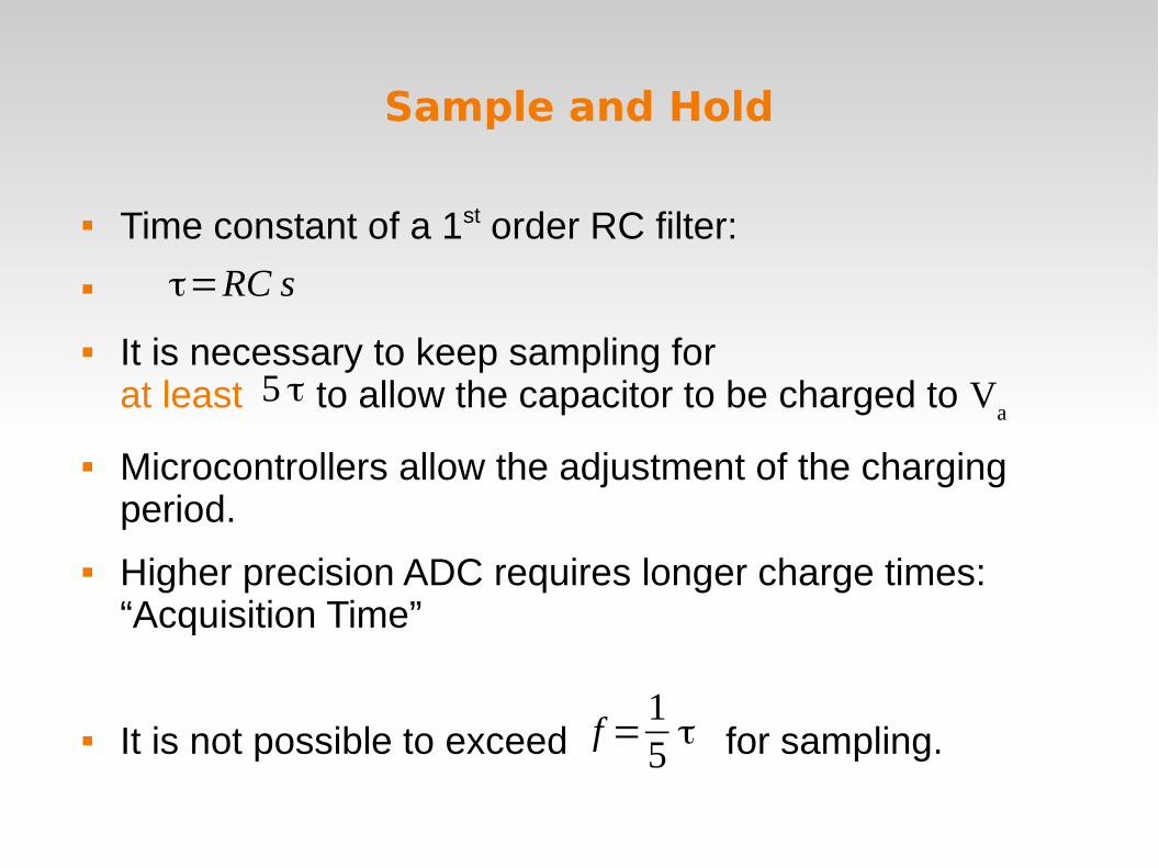
Sample and Hold
Time constant of a 1st order RC filter:
It is necessary to keep sampling for at least to allow the capacitor to be charged to V
a
Microcontrollers allow the adjustment of the charging period.
Higher precision ADC requires longer charge times:“Acquisition Time”
It is not possible to exceed for sampling.
τ=RC s
5 τ
f =15
τ

Sample and Hold
Sampling several signals at the same instant.
Several ADC can be used.
More commonly, synchronoussampling, sequential conversion:
In specialized applicationsseveral ADC are used:Motor current sampling, lab measurement etc.
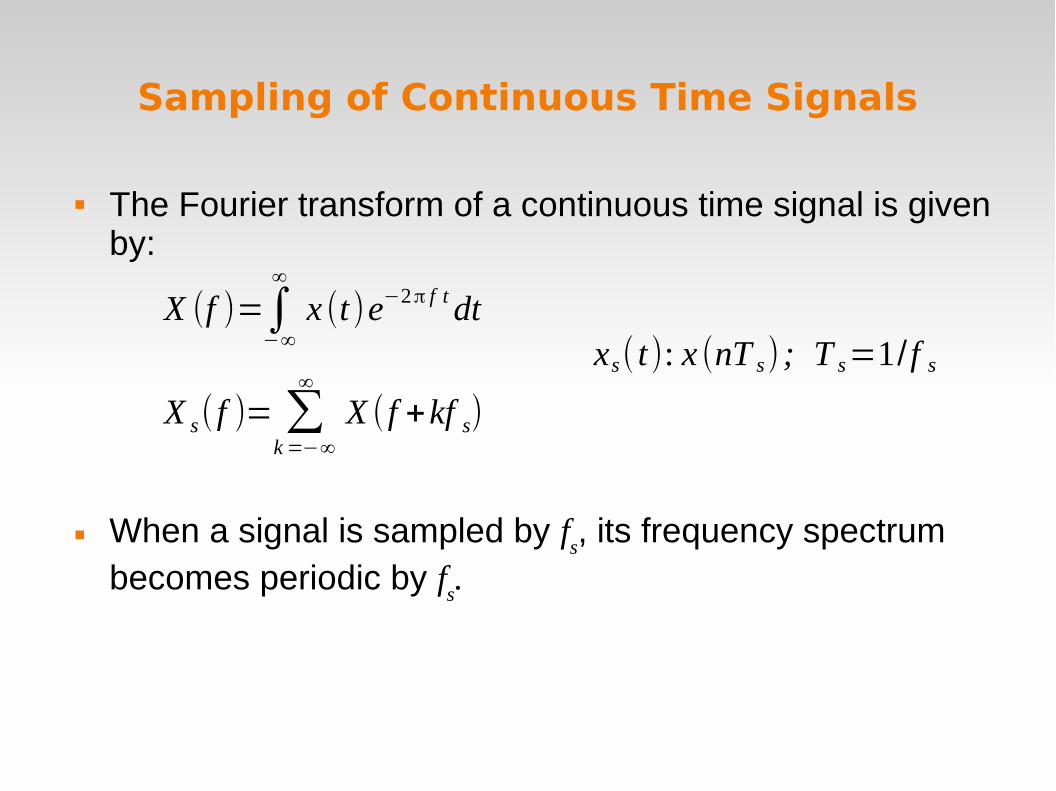
Sampling of Continuous Time Signals
The Fourier transform of a continuous time signal is given by:
When a signal is sampled by fs, its frequency spectrum
becomes periodic by fs.
X (f )=∫−∞
∞
x (t )e−2π f t dt
X s( f )= ∑k =−∞
∞
X ( f +kf s)
xs( t): x (nT s) ; T s=1/ f s

Sampling of Continuous Time Signals
X ( ƒ)
ƒB−B
Continuous time signal frequency spectrum
Sampled. Note spacing
With correct filtering, original signal can be exactly recovered.
Source of figures: Wikipedia.org

Sampling of Continuous Time Signals
However, if low sampling frequency is used:
There are overlaps:
Which are added up.
Original signal is lost.Source of figures: Wikipedia.org
[ (k+1) f s−B , kf s+B ] , k∈−∞ ,∞
X s( f )= ∑k =−∞
∞
X ( f +kf s)

The Data Converter AKA Quantizer
Analog to digital conversion (ADC) is a search operation.
Precision is limited to finite value,
Information about input is lost.
Time consuming OR complex operation.
xq=⌊2N V in
V ref
+Δ2 ⌋
Δ=V ref /2N
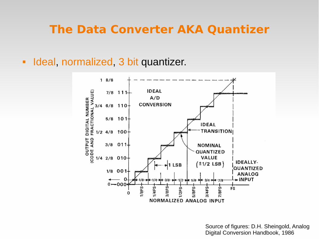
The Data Converter AKA Quantizer
Ideal, normalized, 3 bit quantizer.
Source of figures: D.H. Sheingold, Analog Digital Conversion Handbook, 1986
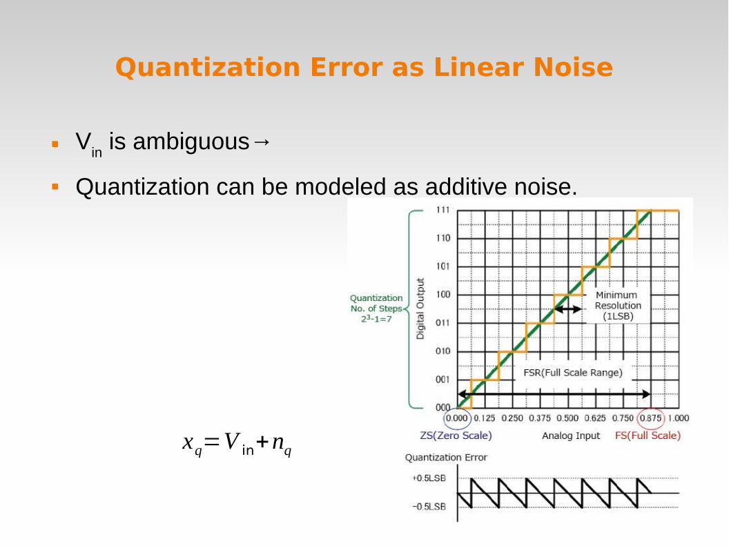
Quantization Error as Linear Noise
Vin is ambiguous→
Quantization can be modeled as additive noise.
xq=V in+nq

Quantization Error as Linear Noise
Vin is not known→
Quantization can be modeled as additive noise.
xq=V in+nq
SNR dB=6.02 N+1.76
(V in=Asin(ω t) , N bit quantizer )
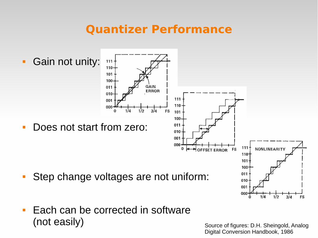
Quantizer Performance
Gain not unity:
Does not start from zero:
Step change voltages are not uniform:
Each can be corrected in software(not easily) Source of figures: D.H. Sheingold, Analog
Digital Conversion Handbook, 1986

Quantizer Realizations: Flash
Low latency
HighcomplexityO(2^N)
Bad linearity
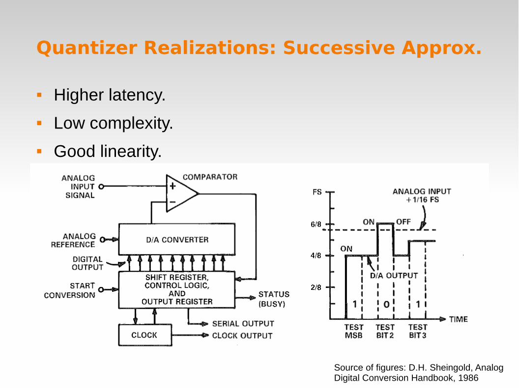
Quantizer Realizations: Successive Approx.
Higher latency.
Low complexity.
Good linearity.
Source of figures: D.H. Sheingold, Analog Digital Conversion Handbook, 1986

Digital Signal Processing
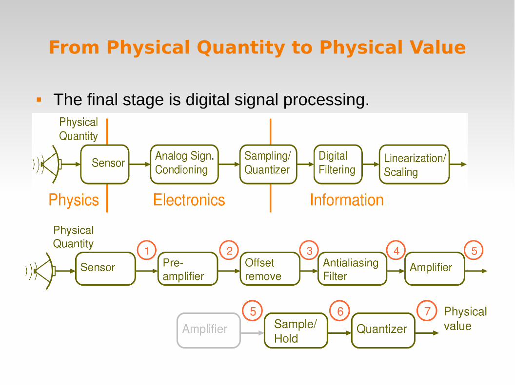
From Physical Quantity to Physical Value
The final stage is digital signal processing.

Oversampling / Noise Shaping
Signal is sampled at much higher rate than Shannon.
After ADC, DSP low pass filter is applied.
Low order anti-aliasing filter is sufficient.
Increase in precision is obtained due to averaging.
S&H +LPF
ωc=π/OSR
ωc↓OSR
nq
V a
Electronics Information
X q
f s=2 f m×OSR

Oversampling / Noise Shaping
Sampling rate is much higher than required by Shannon theorem.
Quantization noise power is constant, regardless of sampling rate.
Signal spectrumamplitude is inreasedproportionally.
Signal occupies lessof the digital bandwith.
V a( f ) '=V a( f )×OSR
f 'max=f max /OSR

Oversampling / Noise Shaping
Downsampling by OSR brings the signal back to desired band.
↓OSR X q

Oversampling / Noise Shaping
Oversampling increases the ADC precision.
OSR= →w bit increase in quantizer precision.
For 4 bit increase: OSR= =256 times oversampling.
44.1KSPS → 11.3MSPS is too much!
Oversampling can be augmented with noise shaping to improve ratio.
4w
44
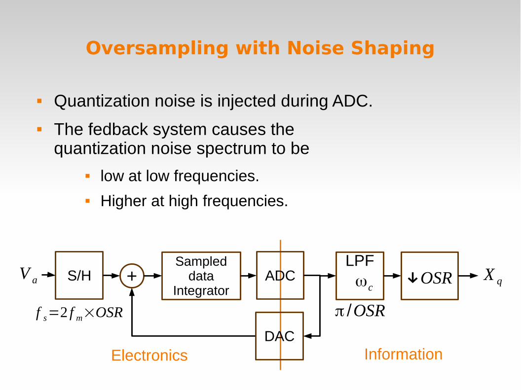
Oversampling with Noise Shaping
Quantization noise is injected during ADC.
The fedback system causes the quantization noise spectrum to be
low at low frequencies. Higher at high frequencies.
Electronics Information
Sampleddata
Integrator+
LPF
π /OSR
ωc↓OSR X q
f s=2 f m×OSR
V a ADC
DAC
S/H

Oversampling with Noise Shaping
The feedback loop has different gains for
quantization noise and Signal.
Quantization noise is concentrated towards higer frequencies.
OSD=8 is sufficient for 4 bit increasevs. OSD=256

High Precision Applications
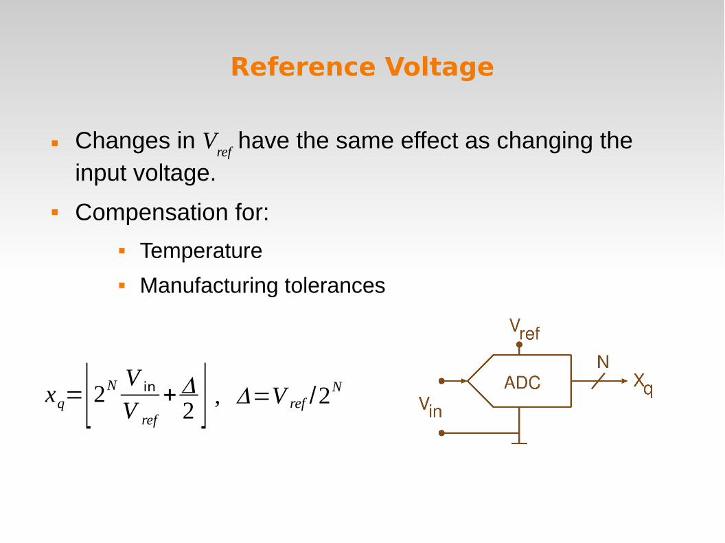
Reference Voltage
Changes in Vref
have the same effect as changing the input voltage.
Compensation for:
Temperature Manufacturing tolerances
xq=⌊2N V in
V ref
+Δ2 ⌋ , Δ=V ref /2
N

Reference Voltage Tolerance
LM336A-2.5: 2.5V reference diode.
2.44 ~ 2.54V at 25o.
8 bit ADC, Vin=1V:
How to calibrate?
V ref =2.44 V → xq=100V ref=2.54 V → xq=104

Reference Voltage Tolerance
Calibration of reference voltage tolerance
1. Multiply by correction coefficient in software
- Firmware in each device must be different.
- In 8 bit processors, correction multiplication is difficult.
2. Electrical adjustment:
- Manual labor
- Long term drift
- Temperature dependence of VR

Common Ground Problems
Microprocessor with daughterboard for temperature sensor.
GND shared between
Daughterboard electronics Sensor voltage
V s=250mV

Common Ground
Connection cables have 1Ω resistance.
Daughterboard draws 50mA current.
ADC reads 20% more: 300mV
V s=250mV
+50 mV

Common Ground
Connection cables have 1Ω resistance.
Daughterboard draws 50mA current.
Ground of the sensor is separated.
Single ground distribution point.
V s=250mV

Secondary Sensors

Secondary Sensors
Electrical component values may change in response to a change in a physical variable.
Change is small; 0.1% or less.
Straightforward measurement of value:
May have large offset error. May depend on other variables (temperature etc.) Require high precision.
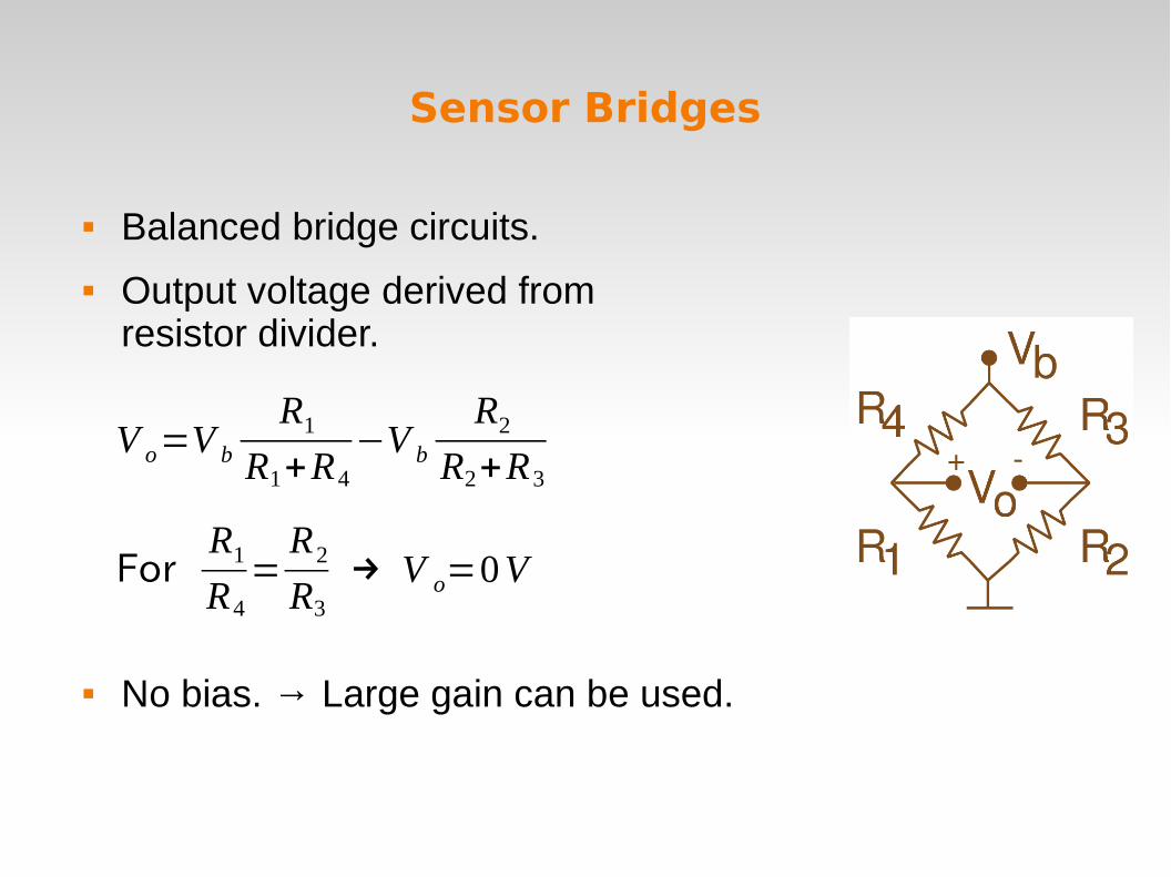
Sensor Bridges
Balanced bridge circuits.
Output voltage derived from resistor divider.
No bias. → Large gain can be used.
V o=V b
R1
R1+R4
−V b
R2
R2+R3
For R1
R4
=R2
R3
→ V o=0 V
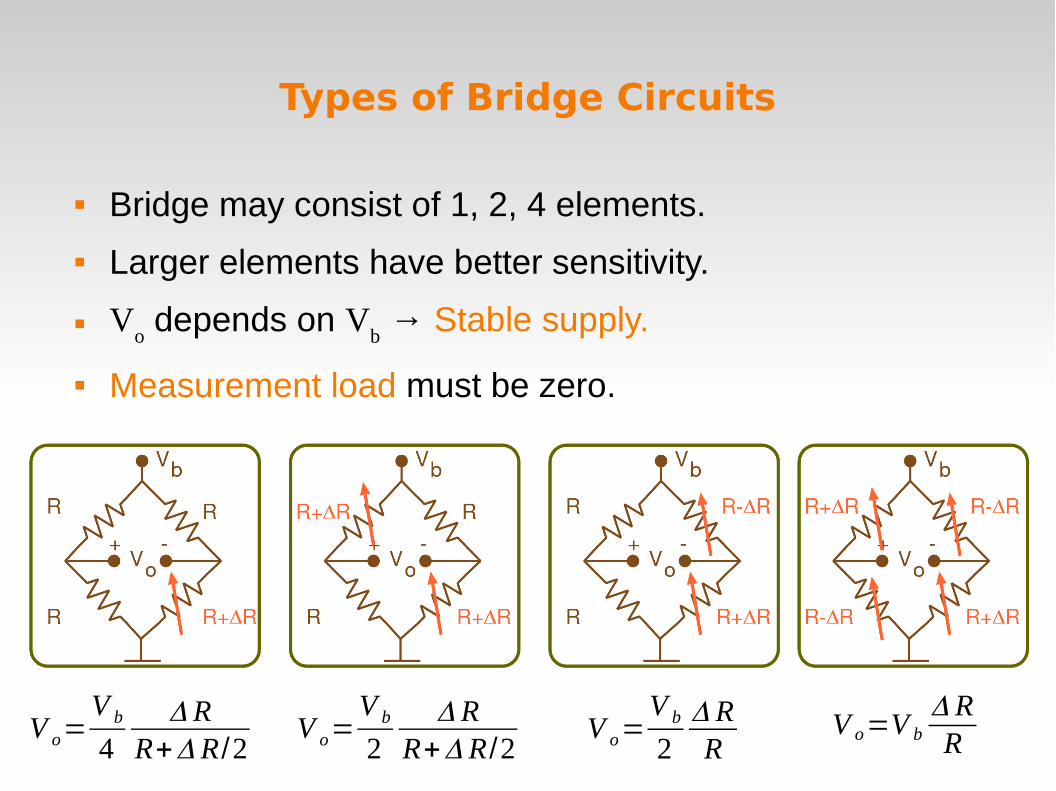
Types of Bridge Circuits
Bridge may consist of 1, 2, 4 elements.
Larger elements have better sensitivity.
Vo depends on V
b → Stable supply.
Measurement load must be zero.
V o=V b
4Δ R
R+Δ R/2V o=
V b
2Δ R
R+Δ R/2V o=
V b
2Δ RR
V o=V bΔ RR

Example Use of Bridge
Strain gage measures bending strain.
R1 and R
2 change in opposite directions.
Stretch measurement eliminated.
V
BRIDGE UNBALANCED
(-)
(+)
R R#1
R#2R
STRAIN GAGE #1
STRAIN GAGE #2
FORCE
+ -
Source of figure: DEWESoft

Amplifiers for Sensor Bridges
Instrumentation amplifier is used.
High input impedance
High CMRR
Gain is set by external resistor Rg. Many good chips exist
AD620 etc.
V o=(V i +−V i -)R1(1+R1
Rg)( R3
R2)
Linearization, Calibration
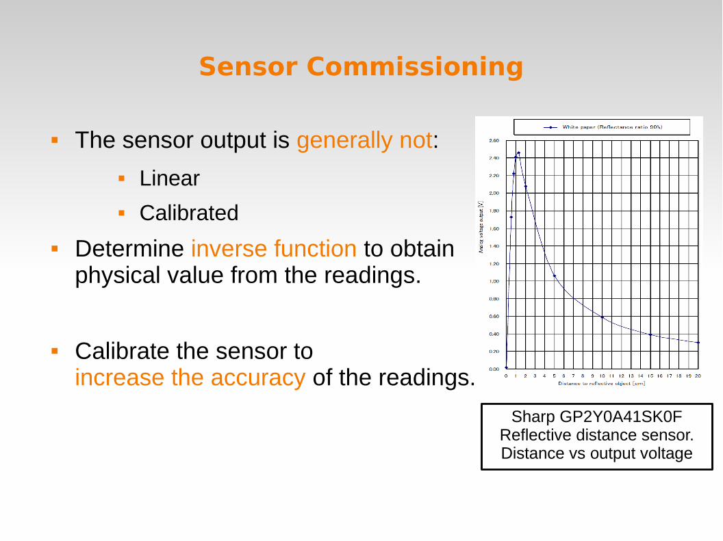
Sensor Commissioning
Sharp GP2Y0A41SK0FReflective distance sensor.Distance vs output voltage
The sensor output is generally not:
Linear Calibrated
Determine inverse function to obtainphysical value from the readings.
Calibrate the sensor to increase the accuracy of the readings.

Linearization
Sensor linear offset and gain correction
Calibration measurements:
Calculate constants:
During runtime:
Periodic calibrations may be needed:Use electronic switch to connect reference.
a1=mp1+ba2=mp2+b
pm=xm−b
m
m=a2−a1
p2−p1
,
b=a1−mp1

Lookup Table – Worst Case
Extreme nonlinearities.
Wasteful of memory. 16bit→ 32bit: 262kB ROM.
STM32F405RGT6: 1MB ROMSTM8s103F: 8kB ROM
If multiple sensors must be fused,even larger footprint.
ADC Physical
0 234
1 200
2 192
3 216
... ...
1022 48
1023 132

Piecewise Linearization
In a certain range of readings,use a specific linearization.
Smaller memory footprint
More run-time computation
Worse error
In Range Slope Offset
a1~a2 m1 b1
a2~a3 m2 b2
a3~a4 m3 b3
a4~a5 m4 b4
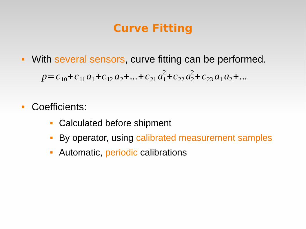
Curve Fitting
With several sensors, curve fitting can be performed.
Coefficients:
Calculated before shipment By operator, using calibrated measurement samples Automatic, periodic calibrations
p=c10+c11 a1+c12 a2+...+c21 a12+c22 a2
2+c23 a1 a2+...

Low power Sensing

Low Power Sensing
Power reduction through low duty cycle.
“Intelligent” sensor with power modes.
Sensor powered down when not needed.
Whole system powered down most of the time.
Source of figure: NXP, “Low-Power Sensing” White Paper.

Low Duty Cycle Operation
Most processors have sleep timers.
Processor consumes power during sleep I/O pins used to power down sensors may keep
consuming power.
Many power management chips are on the market.
TI TPL5110 System timer

Low Duty Cycle Operation
Processor sets sleep time
Timer turns off power:Whole system is switched off.
Processor sleep mode: 1μA
Timer sleep mode: 35nA
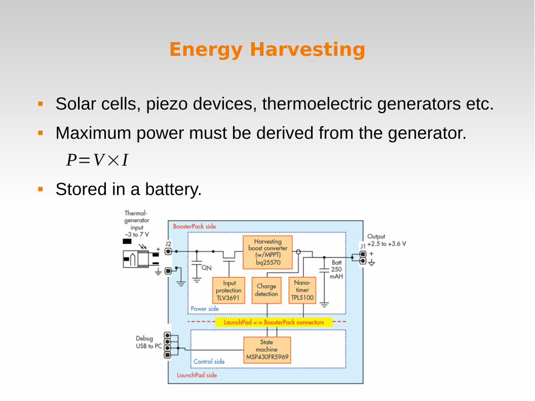
Energy Harvesting
Solar cells, piezo devices, thermoelectric generators etc.
Maximum power must be derived from the generator.
Stored in a battery.
P=V×I

Solar Cell Basics
Efficiency.
8%~45%. General commercial: ~15% Solar Flux: 1kW/m2 noontime. ~150W/m2.
Power output.
More current draw, less voltage.
Track the best V~I ratio. (!)
Power conversion.
Change voltage as required. → buck/boost converter- regulator.
P=V×I

Solar Cell Sizing
Determine
power consumption (Vcc
, Ic)
duty ratio (seconds/hr): Vcc
x Ic x s
→ Energy requirement
Size the battery: 3.7V, 0.5Ah etc.
Size the solar cell:
Use the peak sun hour of deployment location. Budget Safety margin
→Area of the solar cell required.
FLOPs per Watt
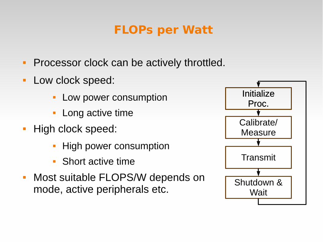
Processor clock can be actively throttled.
Low clock speed:
Low power consumption Long active time
High clock speed:
High power consumption Short active time
Most suitable FLOPS/W depends on mode, active peripherals etc.
InitializeProc.
Calibrate/Measure
InitializeProc.
Transmit
Shutdown &Wait
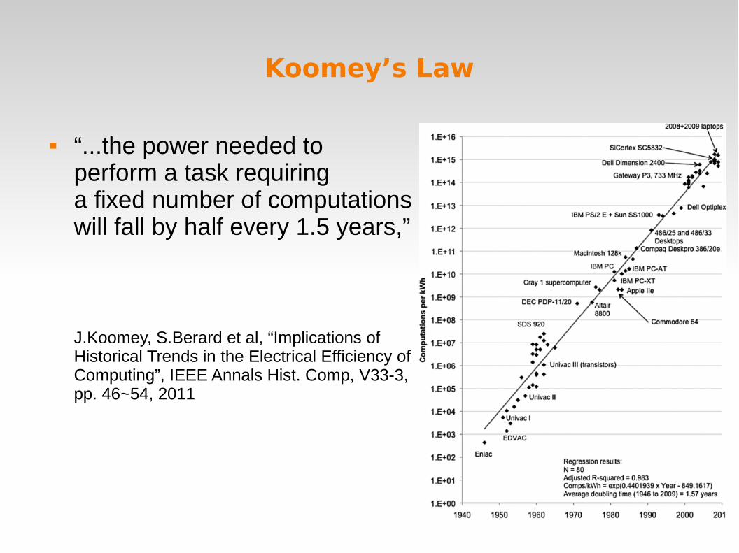
Koomey’s Law
“...the power needed to perform a task requiring a fixed number of computations will fall by half every 1.5 years,”
J.Koomey, S.Berard et al, “Implications of Historical Trends in the Electrical Efficiency of Computing”, IEEE Annals Hist. Comp, V33-3, pp. 46~54, 2011
Integrated Sensors

High Precision Applications
MP5611 barometric pressure sensor. (MEAS Switzerland)
Accurate to 1ft of absolute altitude.
24bit ADC (Δ≈200nV)
Discrete implementation requires expensivesignal conditioning circuits.
Integrated Sensors
High precision applications require great engineering and calibration effort.
Many sensors are offered in:
Sensor + Signal conditioning + Power management + Subsystem control packages
End user connects the sensor over “I2C, “SPI” “CAN” etc.
(Some) References
A.V. Oppenheim, R.W. Schafer, “Discrete-Time Signal Processing”, Prentice-Hall, 2009
Stuart Ball, “Analog Interfacing to Embedded Microprocessor Systems”, Elsevier, 2003
Tattamangalam R. Padmanabhan “Industrial Instrumentation”, Springer, 2000
Paul Pickering, “Designing Ultra-Low-Power Sensor Nodes for IoT Applications”, Texas Instruments, 2006
J.Koomey, S.Berard et al, “Implications of Historical Trends in the Electrical Efficiency of Computing”, IEEE Annals Hist. Comp, V33-3, pp.46~54, 2011
Jack G. Ganssle “The Art of Programming Embedded Systems, Academic Press, 1992
D.H. Sheingold, “Analog Digital Conversion Handbook”, Analog Devices, 1986

Contact Information
Ahmet Onat
Sabanci University, Istanbul, Turkey
Mail: [email protected]
Web: http://people.sabanciuniv.edu/onat

Research projects
I am carrying out projects in
– Reinforcemet learning for dynamic systems
– Networked real-time systems. Internet of Things IoT
– Haptic interfaces for 3D displays
– Linear motor design
– Underwater autonomous robots
See:
http://people.sabanciuniv.edu/onat
Enthusiastic students are welcome to help!

Linear motor elevators
Vertical linear motor design
Project funded by Fujitec, Japan
2007-2013
450kg payload, 1000m length
Prototype, patents, publications
Magnetic, electronic, control, safety design
3meter prototype

Dihedral Corner Reflector Array (DCRA)
A passive optical device
That can create real reflections to form floating imagesin the air
Haptic feedback forprojected solid objects

SWARMS
Modeling of underwarter autonomous vehicles (IoT)

Networked control systems
A novel method for control over networks with unpredictable delay & data loss
Stability analysis, simulation & prototype Tolerant of large amounts of delay Also wireless Ethernet application Publications & prototype control systems
NETWORK
Plant
Controller Node
Actuator NodeSensor Node
Plant

Laboratory work
Will be programming:
ARM prcessor using'C' language
Blink lights,
Move servos,
Communication,
Real-Time OS...