estimating period jitter from phase noise -- an279
TRANSCRIPT
Rev. 0.1 1/07 Copyright © 2007 by Silicon Laboratories AN279Silicon Laboratories Confidential. Information contained herein is covered under non-disclosure agreement (NDA).
AN279
ESTIMATING PERIOD JITTER FROM PHASE NOISE
1. Introduction
This application note reviews how RMS period jitter may be estimated from phase noise data. This approach isuseful for estimating period jitter when sufficiently accurate time domain instruments, such as jitter measuringoscilloscopes or Time Interval Analyzers (TIAs), are unavailable.
2. Terminology
In this application note, the following definitions apply:
Cycle-to-cycle jitter—The short-term variation in clock period between adjacent clock cycles. This jitter measure, abbreviated here as JCC, may be specified as either an RMS or peak-to-peak quantity.
Jitter—Short-term variations of the significant instants of a digital signal from their ideal positions in time(Ref: Telcordia GR-499-CORE). In this application note, the digital signal is a clock source or oscillator. Short-term here means phase noise contributions are restricted to frequencies greater than or equal to 10 Hz(Ref: Telcordia GR-1244-CORE).
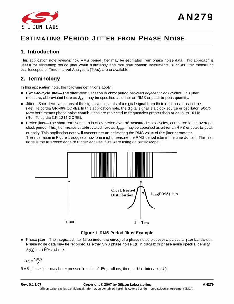
Period jitter—The short-term variation in clock period over all measured clock cycles, compared to the average clock period. This jitter measure, abbreviated here as JPER, may be specified as either an RMS or peak-to-peak quantity. This application note will concentrate on estimating the RMS value of this jitter parameter.The illustration in Figure 1 suggests how one might measure the RMS period jitter in the time domain. The first edge is the reference edge or trigger edge as if we were using an oscilloscope.
Figure 1. RMS Period Jitter Example
Phase jitter—The integrated jitter (area under the curve) of a phase noise plot over a particular jitter bandwidth. Phase noise data may be recorded as either SSB phase noise L(f) in dBc/Hz or phase noise spectral density
S(f) in rad2/Hz where:
RMS phase jitter may be expressed in units of dBc, radians, time, or Unit Intervals (UI).
T = 0
J PER (RMS) =
T = TPER
Clock Period Distribution
L f S f 2
-------------
AN279
2 Rev. 0.1
3. Basic Approach
By definition, period jitter compares two similar instants in time of a clock source such as two successive risingedges or two successive falling edges. Since the two instants are separated in time by approximately one period, itis reasonable to expect that higher frequency jitter components will contribute more to period jitter than lower-frequency jitter components (f<<1/T.)
A number of authors, e.g., Drakhlis (2001), have derived the basic relationship between JPER (rms) and phasenoise spectral density S(f). It can be shown that
and, therefore:
In short, period jitter is integrated similarly to phase jitter but with a frequency weighting factor of 4sin2(f).See "Appendix A—Derivation" on page 5.
There are practical limits to integrating phase noise from f = 0 to Phase noise is measured from a low-frequencylimit, fL, to a high-frequency limit, fH. In practice, the minimum and maximum phase noise offset frequencies aredetermined by the measurement system bandwidth.
Phase noise integration using the sin2 weighting factor is not typically sensitive to contributions from offsetfrequencies well below the half-carrier frequency. Therefore, the choice of fL in theoretical period jitter calculationsis generally not critical. For the purposes of this application note, the minimum offset frequency for phase noisemeasurements is 10 Hz, coinciding with the usual dividing line between wander and jitter.
The period jitter sin2 weighting factor reaches its first maximum at the half-carrier frequency and becomes periodicthereafter. It is clear that phase noise in the vicinity of this offset will make a significant contribution to the periodjitter.
The maximum offset frequency for the purposes of integration is determined by the bandwidth of interest. Onepractical high-frequency limit is to set fH equal to the half-carrier frequency. For an example, see Underhill andBrown (2004). Another, more conservative, approach is to integrate out to the carrier frequency where the sin2
weighting factor reaches its first null. This method appears to correlate well with at least one popular Time IntervalAnalyzer or TIA, presumably due to aliasing components above fC/2. See Smith (2006).
However, in many high-frequency applications, phase noise equipment cannot measure phase noise all the wayout to either the half-carrier or carrier frequencies. Provided that the phase noise data reaches the phase noisefloor at its highest measured offset, the phase noise floor may be extended from fH, MEASURED to fH . This is theestimation approach adopted in this application note.
RMS2
4 S f x 2sin f fd
0
=
JPER rms T0
2------ RMS
2=
AN279
Rev. 0.1 3
4. Example
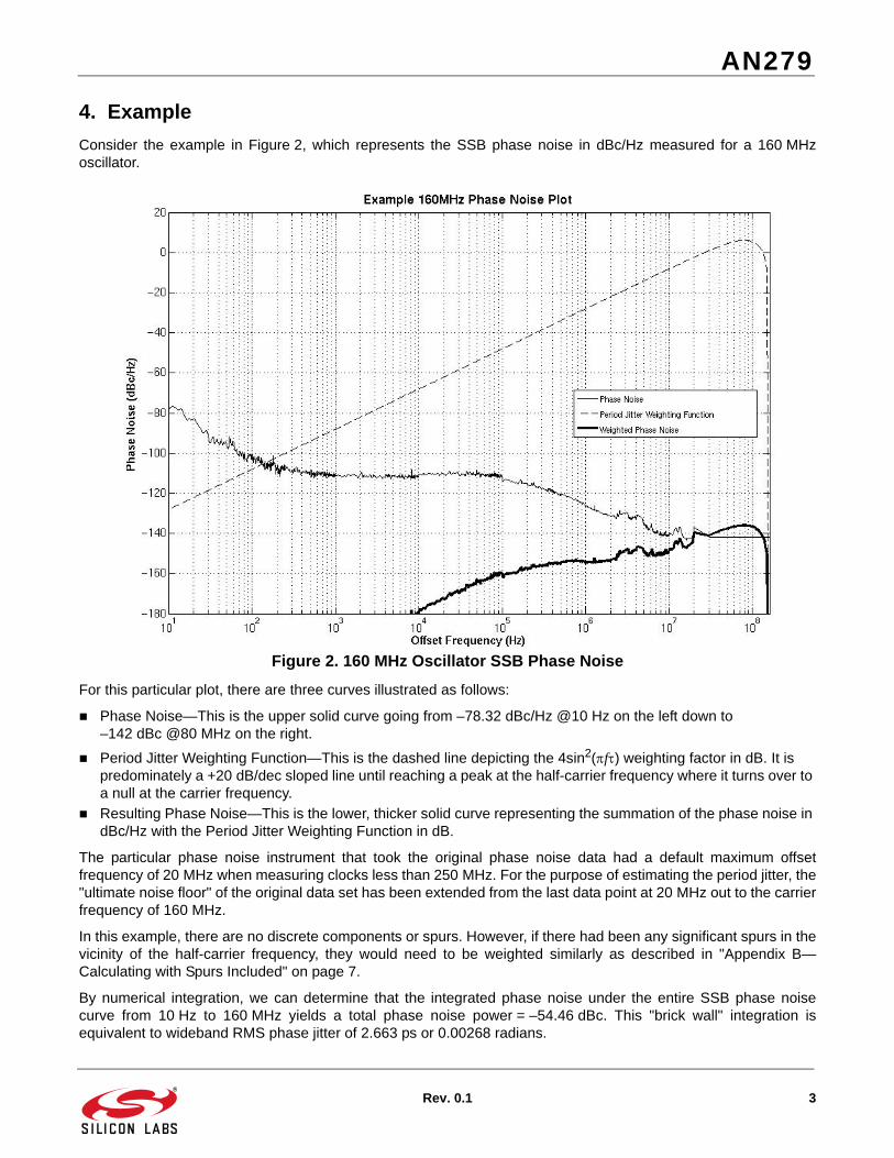
Consider the example in Figure 2, which represents the SSB phase noise in dBc/Hz measured for a 160 MHzoscillator.
Figure 2. 160 MHz Oscillator SSB Phase Noise
For this particular plot, there are three curves illustrated as follows:
Phase Noise—This is the upper solid curve going from –78.32 dBc/Hz @10 Hz on the left down to–142 dBc @80 MHz on the right.
Period Jitter Weighting Function—This is the dashed line depicting the 4sin2(f) weighting factor in dB. It is predominately a +20 dB/dec sloped line until reaching a peak at the half-carrier frequency where it turns over to a null at the carrier frequency.
Resulting Phase Noise—This is the lower, thicker solid curve representing the summation of the phase noise in dBc/Hz with the Period Jitter Weighting Function in dB.
The particular phase noise instrument that took the original phase noise data had a default maximum offsetfrequency of 20 MHz when measuring clocks less than 250 MHz. For the purpose of estimating the period jitter, the"ultimate noise floor" of the original data set has been extended from the last data point at 20 MHz out to the carrierfrequency of 160 MHz.
In this example, there are no discrete components or spurs. However, if there had been any significant spurs in thevicinity of the half-carrier frequency, they would need to be weighted similarly as described in "Appendix B—Calculating with Spurs Included" on page 7.
By numerical integration, we can determine that the integrated phase noise under the entire SSB phase noisecurve from 10 Hz to 160 MHz yields a total phase noise power = –54.46 dBc. This "brick wall" integration isequivalent to wideband RMS phase jitter of 2.663 ps or 0.00268 radians.
AN279
4 Rev. 0.1
By contrast, if we weight L(f) using the period jitter weighting function and integrate the resulting curve over 10 Hzto 160 MHz, we obtain a total phase noise power = –56.84 dBC, equivalent to RMS period jitter of 2.025 ps or0.00204 radians; so, we can estimate the period jitter as being roughly 2 ps RMS, based solely on the availablephase noise measurement. This estimate can be correlated with measurements from complementary time domainequipment when available. See Smith (2006) for example.
The estimation process may be simplified further by treating the period jitter weighting function as if it was a single-pole, high-pass filter function out to fc/2 only. As noted in Figure 2, the JPER weighting function, based on the4sin2(f) weighting factor in dB, looks like a +20 dB/dec sloped line until it gets close to the half-carrier frequency,
where it starts to curve down. If one instead approximates the weighting function as 4(f)2 in dB, this yields astraight +20 dB/dec line. The maximum or intercept at the half-carrier frequency is, therefore,
10log(4((fc/2))2) = 10log(2) = 9.94 dB or approximately 10 dB. Integrating the weighted phase noise in thisfashion, one obtains –57.62 dBc, equivalent to RMS period jitter of 1.849 ps or 0.00186 radians. In this particularexample, the simplified “single pole filter” weighting out to the half carrier frequency resulted in a roughly 9% lowerestimate. This is a less conservative approach, which may still yield a sufficiently accurate estimate depending onthe application.
Since this approach does not directly measure period jitter in the time domain, we cannot make definitivestatements about the peak-to-peak values of the period jitter. However, if other evidence suggests that the edgejitter or period jitter distribution is Gaussian, we can apply the usual statistical estimates.
5. Summary
This application note has reviewed how RMS period jitter may be estimated from phase noise data. The key pointsto keep in mind are as follows:
Period jitter is dominated by high-frequency phase noise.
Channel bandwidth plays a determining role in the apparent jitter observed.
Spurs contribute very little to the period jitter unless they are large and located in the vicinity of the half-carrier frequency.
Generally speaking, hybrid crystal oscillators, such as the Si5xx series devices, have excellent period jitter due totheir relatively low noise floor.
6. References
Drakhlis, Boris, "Calculate Oscillator Jitter By Using Phase-Noise Analysis,"Microwaves & RF, Jan. 2001 pp. 82-90, 157.
Underhill, M. J. and P. J. Brown, "Estimation of Total Jitter and Jitter Probability Density Function from the SignalSpectrum", Proc. 18th EFTF (European Time and Frequency Forum), University of Surrey, Guildford, UK, 5-7 April2004.
Smith, Kevin G., “Practical Issues Correlating Theoretical Period Jitter vs. T1A Measured Period Jitter”, AustinConference on Integrated Systems & Circuits, 2006.
AN279
Rev. 0.1 5
APPENDIX A—DERIVATION
The following calculations are based on the zero crossings derivation of Drakhlis (2001).
Let t represent the jitter accumulated in one period.
Where: T0 = nominal period.
t1 = first zero crossing.
t2 = second zero crossing.
We can drop the T0/2 factor for simplicity and add it back in later.
Per Parseval’s theorem:
Further:
The phase noise autocorrelation equals the cosine transform of the phase noise.
tT0
2------ t1 t2 – ondssec =
t2
T0
2------
2 t1 t2 – 2 =
<2> < t1 2> 2 < t1 > x < t2 >– < t2 2>+ radians2 =
Since t is stationary:
< t1 2> < t2 2> < t 2>= =
< t 2> S f
0
=
< t1 x t2 > R t2 t1– =
< t1 x t2 > R =
Where R is the autocorrelation of f , and T0=
< t1 x t2 > S f 2f dfcos
0
=
RMS2
2 S f 1 2f cos– df
0
=
RMS2
2 S f x 2 2sin f df
0
=
RMS2
4 S f x 2sin f df
0
=
AN279
6 Rev. 0.1
Now, convert back to time units:
where fL and fU are the practical lower and upper frequency integration limits.
RMS2
2x 4 L f 2sin f df
0
=
tRMS2 T0
2------
2RMS
22
T02
2------ L f 2sin f df
0
2T0
2
2------ L f 2sin f df
fL
fU
= = =
JPERRMS t2RMS=
AN279
Rev. 0.1 7
APPENDIX B—CALCULATING WITH SPURS INCLUDED
Spurs that are small and few in number and do not contribute significantly to phase jitter may typically be omittedfrom period jitter calculations. This is especially true for low offset frequency spurs. Each significant spurcontribution should be accounted for separately as for the weighted ith spur below:
Each spur's contributions are then added in sum square fashion as follows:
or:
RMS_i2
8L fi x 2sin fi =
RMS_i2 T0
2------
28L fi 2sin fi
2T02
2------------L fi 2sin fi = =
tRMS_TOTAL2 tRMS_NOISE
2 tRMS_12 tRMS_i
2 tRMS_N2
+ + + + +=
tRMS_TOTAL2 tRMS_NOISE
2 tRMS_i2
i 1=
N
+=
JPER_TOTAL(rms) tRMS_TOTAL2
=
DisclaimerSilicon Laboratories intends to provide customers with the latest, accurate, and in-depth documentation of all peripherals and modules available for system and software implementers using or intending to use the Silicon Laboratories products. Characterization data, available modules and peripherals, memory sizes and memory addresses refer to each specific device, and "Typical" parameters provided can and do vary in different applications. Application examples described herein are for illustrative purposes only. Silicon Laboratories reserves the right to make changes without further notice and limitation to product information, specifications, and descriptions herein, and does not give warranties as to the accuracy or completeness of the included information. Silicon Laboratories shall have no liability for the consequences of use of the information supplied herein. This document does not imply or express copyright licenses granted hereunder to design or fabricate any integrated circuits. The products must not be used within any Life Support System without the specific written consent of Silicon Laboratories. A "Life Support System" is any product or system intended to support or sustain life and/or health, which, if it fails, can be reasonably expected to result in significant personal injury or death. Silicon Laboratories products are generally not intended for military applications. Silicon Laboratories products shall under no circumstances be used in weapons of mass destruction including (but not limited to) nuclear, biological or chemical weapons, or missiles capable of delivering such weapons.
Trademark InformationSilicon Laboratories Inc., Silicon Laboratories, Silicon Labs, SiLabs and the Silicon Labs logo, CMEMS®, EFM, EFM32, EFR, Energy Micro, Energy Micro logo and combinations thereof, "the world’s most energy friendly microcontrollers", Ember®, EZLink®, EZMac®, EZRadio®, EZRadioPRO®, DSPLL®, ISOmodem ®, Precision32®, ProSLIC®, SiPHY®, USBXpress® and others are trademarks or registered trademarks of Silicon Laboratories Inc. ARM, CORTEX, Cortex-M3 and THUMB are trademarks or registered trademarks of ARM Holdings. Keil is a registered trademark of ARM Limited. All other products or brand names mentioned herein are trademarks of their respective holders.
http://www.silabs.com
Silicon Laboratories Inc.400 West Cesar ChavezAustin, TX 78701USA
ClockBuilder Pro
One-click access to Timing tools, documentation, software, source code libraries & more. Available for Windows and iOS (CBGo only).
www.silabs.com/CBPro
Timing Portfoliowww.silabs.com/timing
SW/HWwww.silabs.com/CBPro
Qualitywww.silabs.com/quality
Support and Communitycommunity.silabs.com