phase noise and jitter in digital electronics -...
TRANSCRIPT
Phase noise and jitter in digital electronics
Claudio E. Calosso* and Enrico Rubiola *Division of Optics, INRIM, Torino, Italy
CNRS FEMTO-ST Institute, Besancon, France Home page http://rubiola.org
E-mail: [email protected] and [email protected]
I. INTRODUCTION
We tested a few digital integrated circuits of different tech-nology and families with the ultimate target of understanding low phase noise frequency synthesis. Digital electronics fea-tures simplicity, reproducibility and cost, which is appealing in applications where the lower noise of analog circuits is not mandatory.
A side target of our work is the reduction of phase noise, first, by paralleling numerous gates, as in microwave and RF amplifiers, and second, to de-alias the output as we did in the Λ divider [Calosso.2013]. In the latter case, modern FPGAs make large pipeline possible because of the high toggling frequency (≈1 GHz).
II. NOISE MODEL
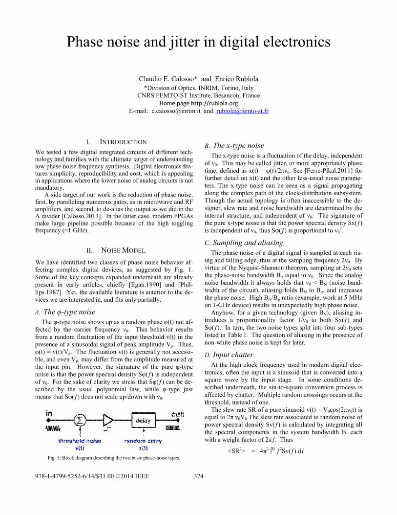
We have identified two classes of phase noise behavior af-fecting complex digital devices, as suggested by Fig. 1. Some of the key concepts expanded underneath are already present in early articles, chiefly [Egan.1990] and [Phil-lips.1987]. Yet, the available literature is anterior to the de-vices we are interested in, and fits only partially.
A. The φ-type noise
The φ-type noise shows up as a random phase φ(t) not af-fected by the carrier frequency ν0. This behavior results from a random fluctuation of the input threshold v(t) in the presence of a sinusoidal signal of peak amplitude Vp. Thus, φ(t) = v(t)/Vp. The fluctuation v(t) is generally not accessi-ble, and even Vp. may differ from the amplitude measured at the input pin. However, the signature of the pure φ-type noise is that the power spectral density Sφ(ƒ) is independent of ν0. For the sake of clarity we stress that Sφ(ƒ) can be de-scribed by the usual polynomial law, while φ-type just means that Sφ(ƒ) does not scale up/down with ν0.
B. The x-type noise
The x-type noise is a fluctuation of the delay, independent of ν0. This may be called jitter, or more appropriately phase time, defined as x(t) = φ(t)/2πν0. See [Ferre-Pikal.2011] for further detail on x(t) and the other less-usual noise parame-ters. The x-type noise can be seen as a signal propagating along the complex path of the clock-distribution subsystem. Though the actual topology is often inaccessible to the de-signer, slew rate and noise bandwidth are determined by the internal structure, and independent of ν0. The signature of the pure x-type noise is that the power spectral density Sx(ƒ) is independent of ν0, thus Sφ(ƒ) is proportional to ν0
2.
C. Sampling and aliasing
The phase noise of a digital signal is sampled at each ris-ing and falling edge, thus at the sampling frequency 2ν0. By virtue of the Nyquist-Shannon theorem, sampling at 2ν0 sets the phase-noise bandwidth Bφ equal to ν0. Since the analog noise bandwidth it always holds that ν0 < BN (noise band-width of the circuit), aliasing folds BN to Bφ, and increases the phase noise. High BN/Bφ ratio (example, work at 5 MHz on 1-GHz device) results in unexpectedly high phase noise.
Anyhow, for a given technology (given BN), aliasing in-troduces a proportionality factor 1/ν0 to both Sx(ƒ) and Sφ(ƒ). In turn, the two noise types split into four sub-types listed in Table I. The question of aliasing in the presence of non-white phase noise is kept for later.
D. Input chatter
At the high clock frequency used in modern digital elec-tronics, often the input is a sinusoid that is converted into a square wave by the input stage. In some conditions de-scribed underneath, the sin-to-square conversion process is affected by chatter. Multiple random crossings occurs at the threshold, instead of one.
The slew rate SR of a pure sinusoid v(t) = V0cos(2πν0t) is equal to 2π ν0V0 The slew rate associated to random noise of power spectral density Sv(ƒ) is calculated by integrating all the spectral components in the system bandwidth B, each with a weight factor of 2πƒ. Thus
<SR2> = 4π2 ∫B ƒ2Sv(ƒ) dƒ
Fig. 1: Block diagram describing the two basic phase-noise types.
978-1-4799-5252-6/14/$31.00 ©2014 IEEE 374
= (4π2/3) σ2 B
The system bandwidth B is of the order of three times the maximum toggling frequency. With a narrower bandwidth, the analog signal could not be converted into a square wave. Chatter occurs when the SR associated to noise exceeds the pure-signal SR at the threshold, so that the slope of the overall signal (sinusoid plus noise) can change sign unpre-dictably. The chatter threshold is given by the equation
ν02 = (Sv B3) / (3 V0
2) A problem with high-speed electronics is that the noise bandwidth B is so wide that chatter may occur in unex-pected conditions. For example, a device toggling at 1 GHz (3 GHz noise bandwidth), having an equivalent input noise of 10 nV/√Hz and driven at 400 mVpp, chatters at ν0 ≤ 4.8 MHz.
In all our experiments, the digital devices are operated out of the chatter region.
III. EXPERIMENTAL METHOD
Checking on the noise model, we measured the devices listed in Table II with a Symmetricom 5125A test set [Mi-rosemi]. The DUT and the test set are driven by the same source, so its noise cancels. Nonetheless we used a high pu-rity synthesizer. We collected noise data scanning the input frequency and changing the internal configuration (HDL program).
IV. SOME RESULTS
A. Cyclone III FPGA
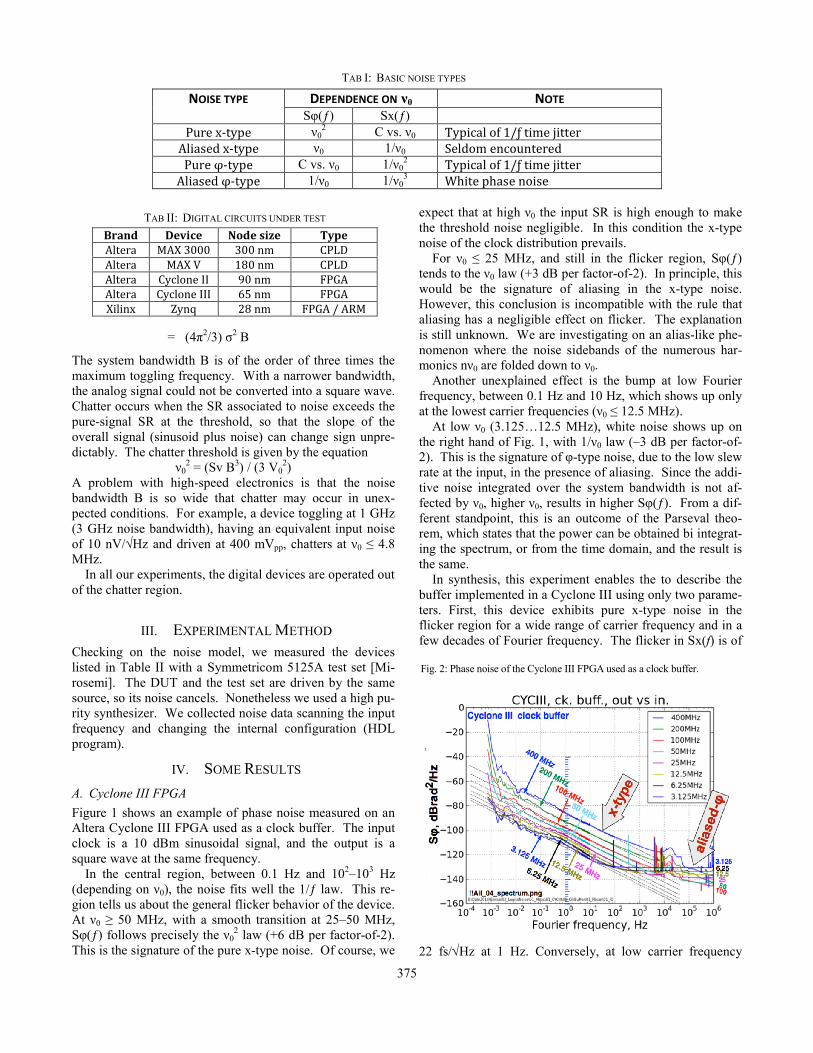
Figure 1 shows an example of phase noise measured on an Altera Cyclone III FPGA used as a clock buffer. The input clock is a 10 dBm sinusoidal signal, and the output is a square wave at the same frequency.
In the central region, between 0.1 Hz and 102–103 Hz (depending on ν0), the noise fits well the 1/ƒ law. This re-gion tells us about the general flicker behavior of the device. At ν0 ≥ 50 MHz, with a smooth transition at 25–50 MHz, Sφ(ƒ) follows precisely the ν0
2 law (+6 dB per factor-of-2). This is the signature of the pure x-type noise. Of course, we
expect that at high ν0 the input SR is high enough to make the threshold noise negligible. In this condition the x-type noise of the clock distribution prevails.
For ν0 ≤ 25 MHz, and still in the flicker region, Sφ(ƒ) tends to the ν0 law (+3 dB per factor-of-2). In principle, this would be the signature of aliasing in the x-type noise. However, this conclusion is incompatible with the rule that aliasing has a negligible effect on flicker. The explanation is still unknown. We are investigating on an alias-like phe-nomenon where the noise sidebands of the numerous har-monics nν0 are folded down to ν0.
Another unexplained effect is the bump at low Fourier frequency, between 0.1 Hz and 10 Hz, which shows up only at the lowest carrier frequencies (ν0 ≤ 12.5 MHz).
At low ν0 (3.125…12.5 MHz), white noise shows up on the right hand of Fig. 1, with 1/ν0 law (–3 dB per factor-of-2). This is the signature of φ-type noise, due to the low slew rate at the input, in the presence of aliasing. Since the addi-tive noise integrated over the system bandwidth is not af-fected by ν0, higher ν0, results in higher Sφ(ƒ). From a dif-ferent standpoint, this is an outcome of the Parseval theo-rem, which states that the power can be obtained bi integrat-ing the spectrum, or from the time domain, and the result is the same.
In synthesis, this experiment enables the to describe the buffer implemented in a Cyclone III using only two parame-ters. First, this device exhibits pure x-type noise in the flicker region for a wide range of carrier frequency and in a few decades of Fourier frequency. The flicker in Sx(f) is of
22 fs/Hz at 1 Hz. Conversely, at low carrier frequency
DEPENDENCE ON ν0 NOTE NOISE TYPE Sφ(ƒ) Sx(ƒ)
Pure x-type ν02 C vs. ν0 Typical of 1/ƒ time jitter
Aliased x-type ν0 1/ν0 Seldom encountered Pure φ-type C vs. ν0 1/ν0
2 Typical of 1/ƒ time jitter Aliased φ-type 1/ν0 1/ν0
3 White phase noise
TAB I: BASIC NOISE TYPES
Fig. 2: Phase noise of the Cyclone III FPGA used as a clock buffer.
TAB II: DIGITAL CIRCUITS UNDER TEST
Brand Device Node size Type Altera MAX 3000 300 nm CPLD Altera MAX V 180 nm CPLD Altera Cyclone II 90 nm FPGA Altera Cyclone III 65 nm FPGA Xilinx Zynq 28 nm FPGA / ARM
375
alias results in -type noise, described by Sφ(ƒ) = k2/ν0. The parameter k can be extracted from Fig. 1. For example, at 12.5 MHz, the white phase noise is of 3.210-14 rad2/Hz, thus k = 630 rad. Assuming that the noise bandwidth is of 3 GHz (three times the maximum toggle frequency), and a peak input voltage of 1 V, after Section II we get a fluctua-tion of 10 nV/√Hz in the analog threshold.
B. Thermal effects It is well known that the charge/discharge cycle if the
gate capacitance results in energy loss E = CV2. Conse-quently, the dissipated power is proportional to ν0, and of course also to the number of gates that switch. As a further consequence, a change in the toggle frequency affects the chip temperature via the junction-ambient thermal resis-tance, and also originates a thermal transient. A moderate thermal insulation was used to prevent the fluctuations of the air flow from spoiling the measured Sφ(ƒ) at low Fourier frequencies. We had to respect a full one-hour delay after each frequency change for the results shown in Fig. 1 to be free from thermal transients.
C. Preliminary conclusions
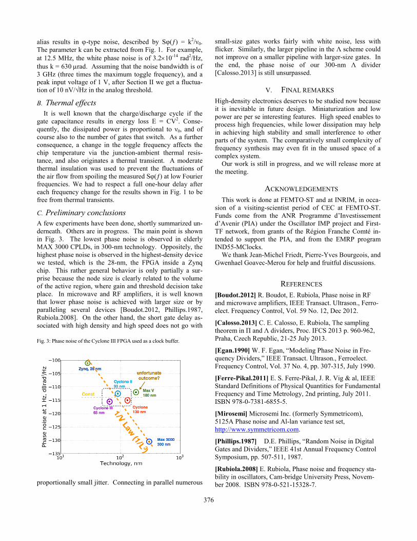
A few experiments have been done, shortly summarized un-derneath. Others are in progress. The main point is shown in Fig. 3. The lowest phase noise is observed in elderly MAX 3000 CPLDs, in 300-nm technology. Oppositely, the highest phase noise is observed in the highest-density device we tested, which is the 28-nm, the FPGA inside a Zynq chip. This rather general behavior is only partially a sur-prise because the node size is clearly related to the volume of the active region, where gain and threshold decision take place. In microwave and RF amplifiers, it is well known that lower phase noise is achieved with larger size or by paralleling several devices [Boudot.2012, Phillips.1987, Rubiola.2008]. On the other hand, the short gate delay as-sociated with high density and high speed does not go with
proportionally small jitter. Connecting in parallel numerous
small-size gates works fairly with white noise, less with flicker. Similarly, the larger pipeline in the Λ scheme could not improve on a smaller pipeline with larger-size gates. In the end, the phase noise of our 300-nm Λ divider [Calosso.2013] is still unsurpassed.
V. FINAL REMARKS
High-density electronics deserves to be studied now because it is inevitable in future design. Miniaturization and low power are per se interesting features. High speed enables to process high frequencies, while lower dissipation may help in achieving high stability and small interference to other parts of the system. The comparatively small complexity of frequency synthesis may even fit in the unused space of a complex system.
Our work is still in progress, and we will release more at the meeting.
ACKNOWLEDGEMENTS
This work is done at FEMTO-ST and at INRIM, in occa-sion of a visiting-scientist period of CEC at FEMTO-ST. Funds come from the ANR Programme d’Investissement d’Avenir (PIA) under the Oscillator IMP project and First-TF network, from grants of the Région Franche Comté in-tended to support the PIA, and from the EMRP program IND55-MClocks.
We thank Jean-Michel Friedt, Pierre-Yves Bourgeois, and Gwenhael Goavec-Merou for help and fruitful discussions.
REFERENCES
[Boudot.2012] R. Boudot, E. Rubiola, Phase noise in RF and microwave amplifiers, IEEE Transact. Ultrason., Ferro-elect. Frequency Control, Vol. 59 No. 12, Dec 2012.
[Calosso.2013] C. E. Calosso, E. Rubiola, The sampling theorem in Π and Λ dividers, Proc. IFCS 2013 p. 960-962, Praha, Czech Republic, 21-25 July 2013.
[Egan.1990] W. F. Egan, “Modeling Phase Noise in Fre-quency Dividers,” IEEE Transact. Ultrason., Ferroelect. Frequency Control, Vol. 37 No. 4, pp. 307-315, July 1990.
[Ferre-Pikal.2011] E. S. Ferre-Pikal, J. R. Vig & al, IEEE Standard Definitions of Physical Quantities for Fundamental Frequency and Time Metrology, 2nd printing, July 2011. ISBN 978-0-7381-6855-5.
[Mirosemi] Microsemi Inc. (formerly Symmetricom), 5125A Phase noise and Al-lan variance test set, http://www.symmetricom.com.
[Phillips.1987] D.E. Phillips, “Random Noise in Digital Gates and Dividers,” IEEE 41st Annual Frequency Control Symposium, pp. 507-511, 1987.
[Rubiola.2008] E. Rubiola, Phase noise and frequency sta-bility in oscillators, Cam-bridge University Press, Novem-ber 2008. ISBN 978-0-521-15328-7.
Fig. 3: Phase noise of the Cyclone III FPGA used as a clock buffer.
376