cdce62005 phase noise and jitter cleaning performance · cdce62005 phase noise performance and...
TRANSCRIPT
Application ReportSCAA095–November 2008
CDCE62005 Phase Noise Performance and Jitter CleaningAbility
Madhu Balasubramanian......................................................................................... Serial Link Products
ABSTRACTThis application report presents phase noise data taken on the Texas Instruments'CDCE62005 jitter cleaner and synchronizer PLL. The phase noise performance of theCDCE62005 depends both on the phase noise of the reference clock and theCDCE62005 itself. This application report shows the phase noise performance at themost popular CDMA frequencies and helps the user to choose the right clockingsolution for their particular applications. These test results confirm that the CDCE62005can provide clocks better than –145dBc/Hz phase noise at 10-MHz offset from thecarrier frequency. Low phase noise is a requirement for wireless applications as well asmany other high-performance sampling systems. The report also reviews the open-loopVCO performance of the CDCE62005 device.
Contents1 Introduction .......................................................................................... 22 Test Equipment and Setup ........................................................................ 33 Total Phase Noise Measurements ............................................................... 44 Jitter Cleaner Measurements ..................................................................... 85 On-Chip Open-Loop VCO Phase Noise Measurements..................................... 11
List of Figures
1 Phase Noise Measurement Test Setup.......................................................... 32 On-Chip Loop Filter Circuit for 400-kHz Loop Bandwidth ..................................... 43 Partial On-Chip Loop Filter Circuit for 100-Hz Loop Bandwidth .............................. 44 491.52-MHz HS-LVPECL Output Phase Noise................................................. 55 122.88-MHz HS-LVPECL Output Phase Noise................................................. 66 61.44-MHz HS-LVPECL Output Phase Noise .................................................. 77 122.88-MHz HS-LVPECL Output Jitter Cleaning Ability....................................... 88 30.72-MHz LVCMOS Input Phase Noise Profile (50 ps, RMS) .............................. 99 122.88-MHz HS-LVPECL Output Phase Noise Profile (50 ps, RMS Input) ............... 1010 Open-Loop Phase Noise of On-Chip VCO1 (Prescaler Divider 3, Output Divider 1) .... 1111 Open-Loop Phase Noise of On-Chip VCO2 (Prescaler Divider 3, Output Divider 1) .... 1212 Open-Loop Phase Noise of On-Chip VCO1 (Prescaler Divider 2, Output Divider 1) .... 1313 Open-Loop Phase Noise of On-Chip VCO2 (Prescaler Divider 2, Output Divider 1) .... 14
E5052A, HP6624A are trademarks of Agilent Technologies.All other trademarks are the property of their respective owners.
SCAA095–November 2008 CDCE62005 Phase Noise Performance and Jitter Cleaning Ability 1Submit Documentation Feedback
1 Introduction
1.1 Definitions
Introduction www.ti.com
The CDCE62005 is a low phase noise, low jitter clock synthesizer and jitter cleaner with programmableoutputs and inputs. It features a phase-locked loop (PLL) architecture with an on-chip voltage-controlledoscillator (VCO) and internal loop filter. An optional external low-pass loop filter is required to complete thePLL. Proper selection of the VCO frequency and loop bandwidth are critical to achieve the bestperformance from the CDCE62005.
This report includes phase noise plots of many of the most common frequencies used in wireless basestation applications. In addition, the phase noise of the open loop VCO of the CDCE62005 is included forcompleteness. The phase noise of the 30.72-MHz reference and output phase noise of the CDCE62005 atvarious frequencies are also included. The RMS jitter was calculated from the phase noise plots measuredover a 10-kHz to 20-MHz range using the Agilent E5052A™ phase noise analyzer.
Timing budget—Defined by dynamic (jitter) and static errors (skew). Depending on the systemarchitecture, only a subset of parameters from the datasheet affects the timing budget. Jitter is atiming distribution of the clock signal that expresses the edge deviation from the ideal occurrence.Jitter is composed of both deterministic and random (Gaussian) content.
Jitter— Any edge deviation from the ideal occurrence. The causes of jitter include: power-supply noise,thermal and mechanical noise from the input signal and other external sources, reflection,electromagnetic interference (EMI), and other random noise. Suggestions to reduce jitter include:power-supply bypassing (10 µF to 47 µF) to prevent voltage droop and ripple because of currentsurges; filtering each VCC pin (with a 0.1-µF, low effective series resistance [ESR] capacitor); usingproper termination to remove reflections; using differential signaling as opposed to single-endedsignaling; and minimizing noise coupling by isolating other high-frequency signals from the clockdriver.
Phase noise—The short-term instability caused by frequency variation (phase) of a signal referenced tothe carrier level and a function of the carrier offset (that is, relative noise level within a 1-Hzbandwidth). Integration of phase noise (PN) over a given frequency band yields phase jitter RMS.
Phase jitter— Phase jitter, or accumulated jitter, is the absolute deviation of a clock edge from its idealposition in timing. While period jitter only accounts for the variation between clock periods, phasejitter accumulates the error of each period and is therefore always larger. The wider the recordingtime window, the more frequency bandwidth becomes integrated into the total phase jitter. Phasejitter can also be measured by integrating phase noise over the frequency band of interest. Eitherway, the system designer must specify the minimum and maximum frequency for the integration.For setup and hold time budget calculations, the peak-to-peak (PP) value of the phase jitter isimportant. Note that only the added phase noise by the clock driver is of interest to find the worstedge position between the master clock in the system and the subsystem. The absolute phase jitterof the master clock itself adds to all clock signals in the system, thus canceling its effect.
Period jitter—The deviation in cycle time of a signal with respect to an ideal period over a randomsample of cycles. Period jitter is important because it includes the maximum and minimumfrequencies, and it specifies the shortest clock period. It is important for the setup and hold timebudgets. Calculations with period jitter are sufficient for subsystems that use clock and data signalsderived from the same clock source. Period jitter can be measured with any oscilloscope.
Peak-to-peak period jitter—The total jitter range from minimum to maximum values of a clock signal.Peak-to-peak (PP) jitter increases indefinitely with recording time. Thus, PP jitter values are onlymeaningful if either the recording length or the relative bit error rate is known.
RMS period jitter—One standard deviation (1 σ) of the peak-to-peak jitter of a clock signal. RMS jitter isonly valid for Gaussian (that is, normal) distribution. RMS jitter is independent of the samplingwindow, and therefore more suitable for comparing the performance of two or more devices wherethe sampling time window differs or is unknown.
2 CDCE62005 Phase Noise Performance and Jitter Cleaning Ability SCAA095–November 2008Submit Documentation Feedback
2 Test Equipment and Setup
Power SupplyHP6624A PC
OscilloscopeTDS694C
Phase Noise AnalyzerE5052A
CDCE62005EVM
CDCE62005
PassiveFilter
HP8133Signal Generator
SPI
REF_IN
Y0
Y0B
www.ti.com Test Equipment and Setup
Cycle-to-cycle period jitter—Also known as adjacent cycle jitter; the variation in cycle time of a signalbetween consecutive cycles over a random sample of successive cycle pairs. Cycle-to-cycle jitter isalso a good value to calculate the setup and hold time budgets because it defines the minimum andmaximum variations of the timing variation from ideal for the next clock edge.
Crosstalk— This characteristic is used to measure parasitic coupling between signals, and is the effect ofcapacitive coupling that causes a logic transition. Capacitive coupling is the transfer of energybetween nearby switching integrated circuits. The coupling depends on factors such as the distancebetween the traces, the signal swing, the operating frequency, and the permissiveness of the silicondioxide. Coupling can be improved by physically increasing the distance between traces. Powerand ground planes also act as shields to minimize crosstalk.
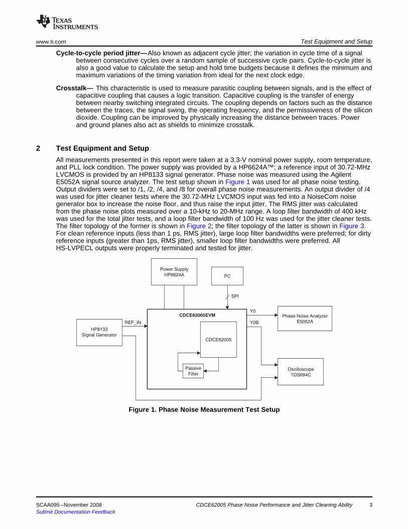
All measurements presented in this report were taken at a 3.3-V nominal power supply, room temperature,and PLL lock condition. The power supply was provided by a HP6624A™; a reference input of 30.72-MHzLVCMOS is provided by an HP8133 signal generator. Phase noise was measured using the AgilentE5052A signal source analyzer. The test setup shown in Figure 1 was used for all phase noise testing.Output dividers were set to /1, /2, /4, and /8 for overall phase noise measurements. An output divider of /4was used for jitter cleaner tests where the 30.72-MHz LVCMOS input was fed into a NoiseCom noisegenerator box to increase the noise floor, and thus raise the input jitter. The RMS jitter was calculatedfrom the phase noise plots measured over a 10-kHz to 20-MHz range. A loop filter bandwidth of 400 kHzwas used for the total jitter tests, and a loop filter bandwidth of 100 Hz was used for the jitter cleaner tests.The filter topology of the former is shown in Figure 2; the filter topology of the latter is shown in Figure 3.For clean reference inputs (less than 1 ps, RMS jitter), large loop filter bandwidths were preferred; for dirtyreference inputs (greater than 1ps, RMS jitter), smaller loop filter bandwidths were preferred. AllHS-LVPECL outputs were properly terminated and tested for jitter.
Figure 1. Phase Noise Measurement Test Setup
SCAA095–November 2008 CDCE62005 Phase Noise Performance and Jitter Cleaning Ability 3Submit Documentation Feedback
C3
0 pF
R3
10 kW
R2
24 kW
C2
473.5 pF
C1
0 pF
C3
21.5 pF
R3
10 kW
R2
5 W
C2
47 Fm
C1
19.5 pF
C4
4.7 Fm
3 Total Phase Noise Measurements
3.1 Phase Noise Measurement Summary
Total Phase Noise Measurements www.ti.com
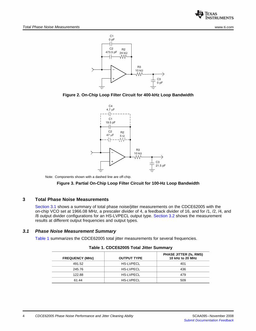
Figure 2. On-Chip Loop Filter Circuit for 400-kHz Loop Bandwidth
Note: Components shown with a dashed line are off-chip.
Figure 3. Partial On-Chip Loop Filter Circuit for 100-Hz Loop Bandwidth
Section 3.1 shows a summary of total phase noise/jitter measurements on the CDCE62005 with theon-chip VCO set at 1966.08 MHz, a prescaler divider of 4, a feedback divider of 16, and for /1, /2, /4, and/8 output divider configurations for an HS-LVPECL output type. Section 3.2 shows the measurementresults at different output frequencies and output types.
Table 1 summarizes the CDCE62005 total jitter measurements for several frequencies.
Table 1. CDCE62005 Total Jitter SummaryPHASE JITTER (fs, RMS)
FREQUENCY (MHz) OUTPUT TYPE 10 kHz to 20 MHz491.52 HS-LVPECL 401245.76 HS-LVPECL 436122.88 HS-LVPECL 47961.44 HS-LVPECL 509
CDCE62005 Phase Noise Performance and Jitter Cleaning Ability4 SCAA095–November 2008Submit Documentation Feedback
3.2 Phase Noise Measurement Results
www.ti.com Total Phase Noise Measurements
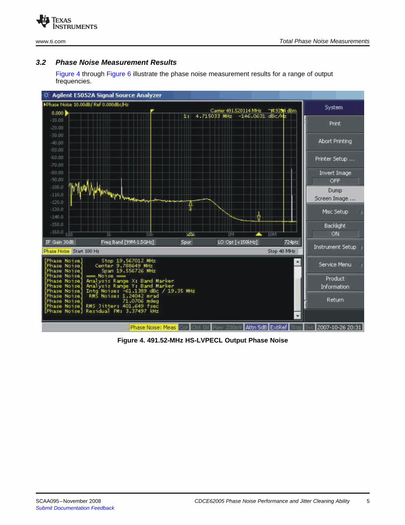
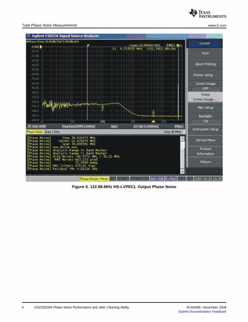
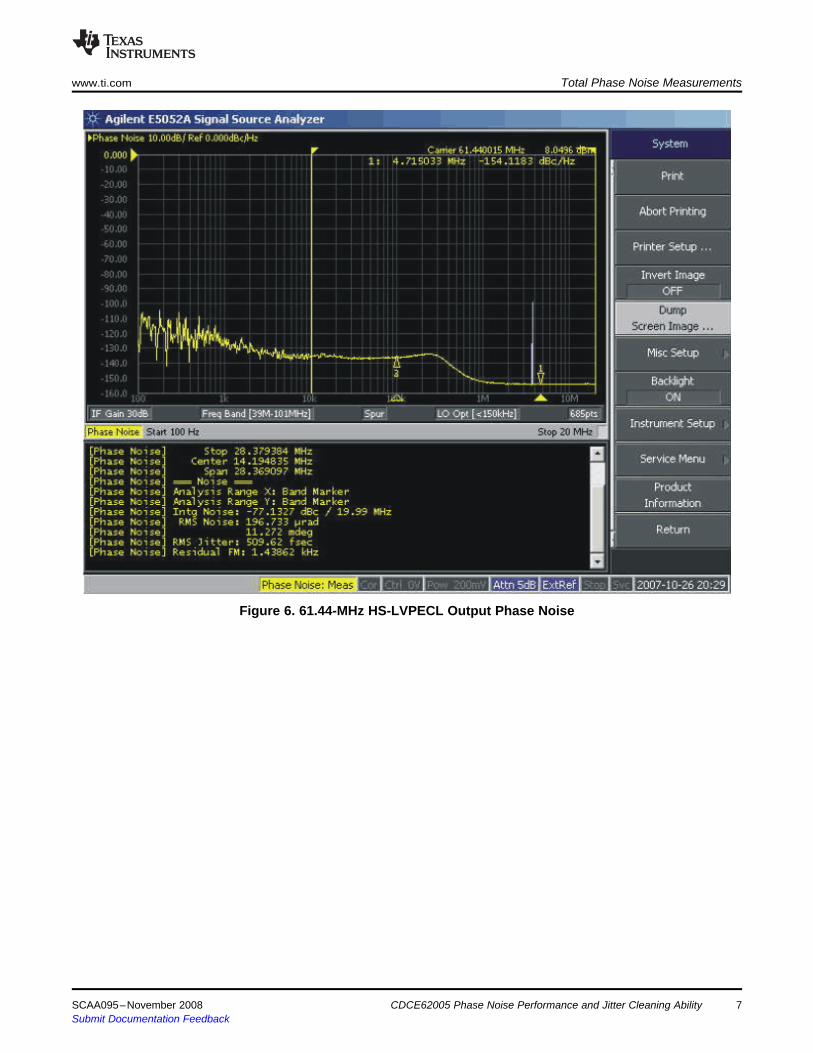
Figure 4 through Figure 6 illustrate the phase noise measurement results for a range of outputfrequencies.
Figure 4. 491.52-MHz HS-LVPECL Output Phase Noise
SCAA095–November 2008 CDCE62005 Phase Noise Performance and Jitter Cleaning Ability 5Submit Documentation Feedback
Total Phase Noise Measurements www.ti.com
Figure 5. 122.88-MHz HS-LVPECL Output Phase Noise
CDCE62005 Phase Noise Performance and Jitter Cleaning Ability6 SCAA095–November 2008Submit Documentation Feedback
www.ti.com Total Phase Noise Measurements
Figure 6. 61.44-MHz HS-LVPECL Output Phase Noise
SCAA095–November 2008 CDCE62005 Phase Noise Performance and Jitter Cleaning Ability 7Submit Documentation Feedback
4 Jitter Cleaner Measurements
4.1 Jitter Cleaner Measurement Summary
10
9
8
7
6
5
4
3
2
1
0
Outp
ut Jitte
r (p
s, R
MS
)
Input Jitter (ps, RMS)
1 11 21 31 41 51
INPUT JITTER vs OUTPUT JITTER
Jitter Cleaner Measurements www.ti.com
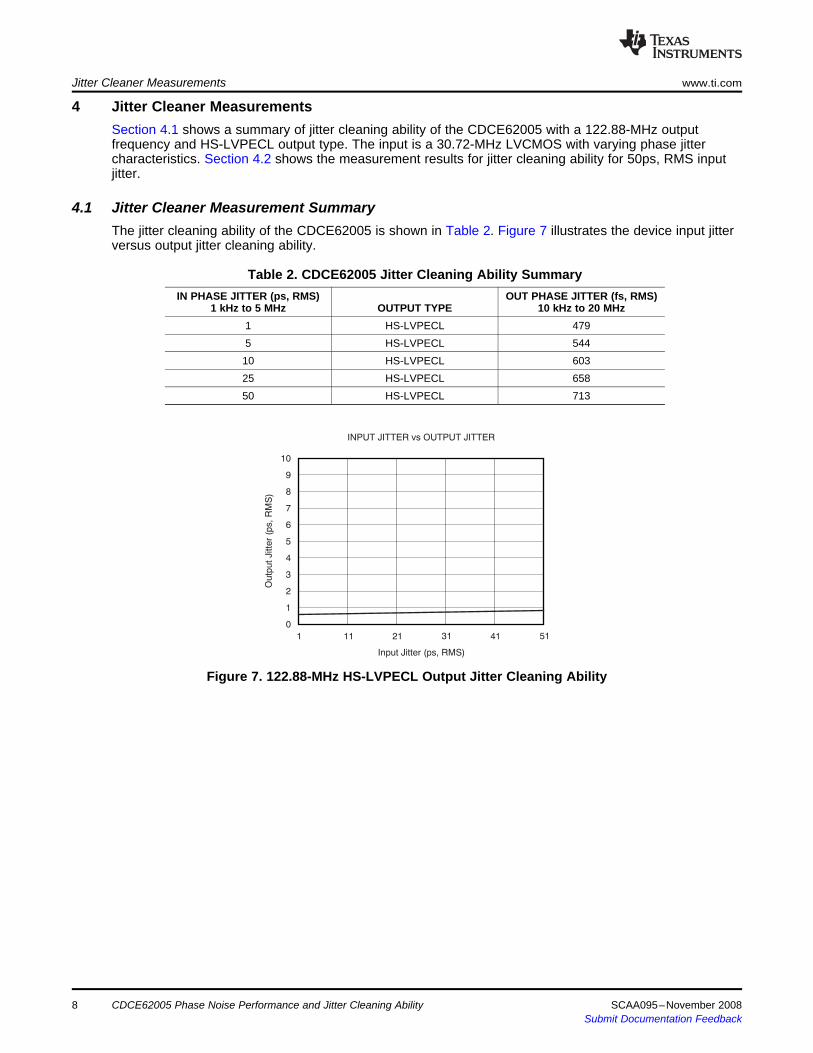
Section 4.1 shows a summary of jitter cleaning ability of the CDCE62005 with a 122.88-MHz outputfrequency and HS-LVPECL output type. The input is a 30.72-MHz LVCMOS with varying phase jittercharacteristics. Section 4.2 shows the measurement results for jitter cleaning ability for 50ps, RMS inputjitter.
The jitter cleaning ability of the CDCE62005 is shown in Table 2. Figure 7 illustrates the device input jitterversus output jitter cleaning ability.
Table 2. CDCE62005 Jitter Cleaning Ability SummaryIN PHASE JITTER (ps, RMS) OUT PHASE JITTER (fs, RMS)
1 kHz to 5 MHz OUTPUT TYPE 10 kHz to 20 MHz1 HS-LVPECL 4795 HS-LVPECL 54410 HS-LVPECL 60325 HS-LVPECL 65850 HS-LVPECL 713
Figure 7. 122.88-MHz HS-LVPECL Output Jitter Cleaning Ability
CDCE62005 Phase Noise Performance and Jitter Cleaning Ability8 SCAA095–November 2008Submit Documentation Feedback
4.2 Jitter Cleaner Measurement Resultswww.ti.com Jitter Cleaner Measurements
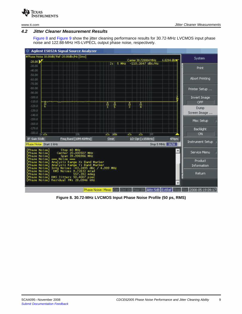
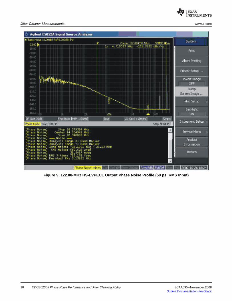
Figure 8 and Figure 9 show the jitter cleaning performance results for 30.72-MHz LVCMOS input phasenoise and 122.88-MHz HS-LVPECL output phase noise, respectively.
Figure 8. 30.72-MHz LVCMOS Input Phase Noise Profile (50 ps, RMS)
SCAA095–November 2008 CDCE62005 Phase Noise Performance and Jitter Cleaning Ability 9Submit Documentation Feedback
Jitter Cleaner Measurements www.ti.com
Figure 9. 122.88-MHz HS-LVPECL Output Phase Noise Profile (50 ps, RMS Input)
CDCE62005 Phase Noise Performance and Jitter Cleaning Ability10 SCAA095–November 2008Submit Documentation Feedback
5 On-Chip Open-Loop VCO Phase Noise Measurements
5.1 Phase Noise Measurement Results
www.ti.com On-Chip Open-Loop VCO Phase Noise Measurements
Section 5.1 shows the measurement results of the open-loop VCO performance of both the on-chip VCOspresent in the CDCE62005 under different test conditions.
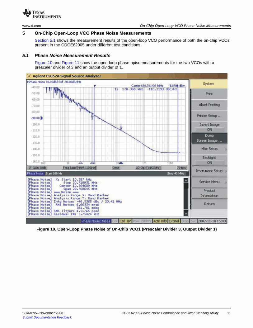
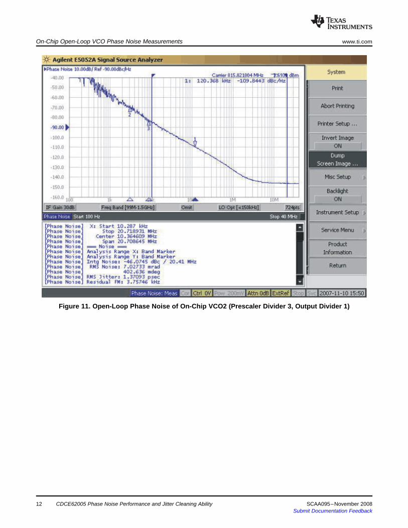
Figure 10 and Figure 11 show the open-loop phase npise measurements for the two VCOs with aprescaler divider of 3 and an output divider of 1.
Figure 10. Open-Loop Phase Noise of On-Chip VCO1 (Prescaler Divider 3, Output Divider 1)
SCAA095–November 2008 CDCE62005 Phase Noise Performance and Jitter Cleaning Ability 11Submit Documentation Feedback
On-Chip Open-Loop VCO Phase Noise Measurements www.ti.com
Figure 11. Open-Loop Phase Noise of On-Chip VCO2 (Prescaler Divider 3, Output Divider 1)
CDCE62005 Phase Noise Performance and Jitter Cleaning Ability12 SCAA095–November 2008Submit Documentation Feedback
www.ti.com On-Chip Open-Loop VCO Phase Noise Measurements
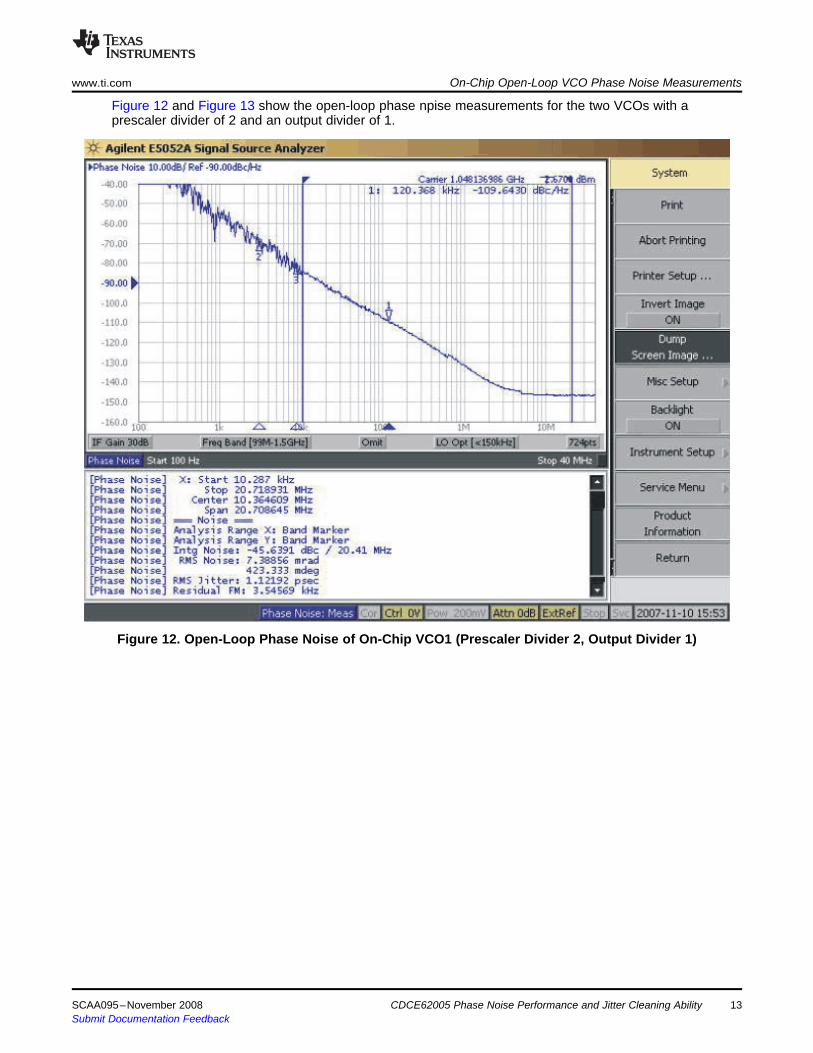
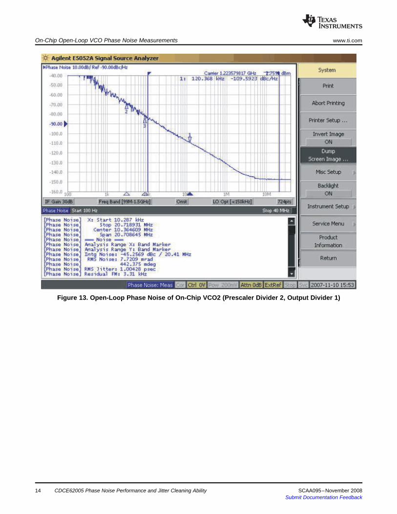
Figure 12 and Figure 13 show the open-loop phase npise measurements for the two VCOs with aprescaler divider of 2 and an output divider of 1.
Figure 12. Open-Loop Phase Noise of On-Chip VCO1 (Prescaler Divider 2, Output Divider 1)
SCAA095–November 2008 CDCE62005 Phase Noise Performance and Jitter Cleaning Ability 13Submit Documentation Feedback
On-Chip Open-Loop VCO Phase Noise Measurements www.ti.com
Figure 13. Open-Loop Phase Noise of On-Chip VCO2 (Prescaler Divider 2, Output Divider 1)
CDCE62005 Phase Noise Performance and Jitter Cleaning Ability14 SCAA095–November 2008Submit Documentation Feedback
IMPORTANT NOTICETexas Instruments Incorporated and its subsidiaries (TI) reserve the right to make corrections, modifications, enhancements, improvements,and other changes to its products and services at any time and to discontinue any product or service without notice. Customers shouldobtain the latest relevant information before placing orders and should verify that such information is current and complete. All products aresold subject to TI’s terms and conditions of sale supplied at the time of order acknowledgment.TI warrants performance of its hardware products to the specifications applicable at the time of sale in accordance with TI’s standardwarranty. Testing and other quality control techniques are used to the extent TI deems necessary to support this warranty. Except wheremandated by government requirements, testing of all parameters of each product is not necessarily performed.TI assumes no liability for applications assistance or customer product design. Customers are responsible for their products andapplications using TI components. To minimize the risks associated with customer products and applications, customers should provideadequate design and operating safeguards.TI does not warrant or represent that any license, either express or implied, is granted under any TI patent right, copyright, mask work right,or other TI intellectual property right relating to any combination, machine, or process in which TI products or services are used. Informationpublished by TI regarding third-party products or services does not constitute a license from TI to use such products or services or awarranty or endorsement thereof. Use of such information may require a license from a third party under the patents or other intellectualproperty of the third party, or a license from TI under the patents or other intellectual property of TI.Reproduction of TI information in TI data books or data sheets is permissible only if reproduction is without alteration and is accompaniedby all associated warranties, conditions, limitations, and notices. Reproduction of this information with alteration is an unfair and deceptivebusiness practice. TI is not responsible or liable for such altered documentation. Information of third parties may be subject to additionalrestrictions.Resale of TI products or services with statements different from or beyond the parameters stated by TI for that product or service voids allexpress and any implied warranties for the associated TI product or service and is an unfair and deceptive business practice. TI is notresponsible or liable for any such statements.TI products are not authorized for use in safety-critical applications (such as life support) where a failure of the TI product would reasonablybe expected to cause severe personal injury or death, unless officers of the parties have executed an agreement specifically governingsuch use. Buyers represent that they have all necessary expertise in the safety and regulatory ramifications of their applications, andacknowledge and agree that they are solely responsible for all legal, regulatory and safety-related requirements concerning their productsand any use of TI products in such safety-critical applications, notwithstanding any applications-related information or support that may beprovided by TI. Further, Buyers must fully indemnify TI and its representatives against any damages arising out of the use of TI products insuch safety-critical applications.TI products are neither designed nor intended for use in military/aerospace applications or environments unless the TI products arespecifically designated by TI as military-grade or "enhanced plastic." Only products designated by TI as military-grade meet militaryspecifications. Buyers acknowledge and agree that any such use of TI products which TI has not designated as military-grade is solely atthe Buyer's risk, and that they are solely responsible for compliance with all legal and regulatory requirements in connection with such use.TI products are neither designed nor intended for use in automotive applications or environments unless the specific TI products aredesignated by TI as compliant with ISO/TS 16949 requirements. Buyers acknowledge and agree that, if they use any non-designatedproducts in automotive applications, TI will not be responsible for any failure to meet such requirements.Following are URLs where you can obtain information on other Texas Instruments products and application solutions:Products ApplicationsAmplifiers amplifier.ti.com Audio www.ti.com/audioData Converters dataconverter.ti.com Automotive www.ti.com/automotiveDSP dsp.ti.com Broadband www.ti.com/broadbandClocks and Timers www.ti.com/clocks Digital Control www.ti.com/digitalcontrolInterface interface.ti.com Medical www.ti.com/medicalLogic logic.ti.com Military www.ti.com/militaryPower Mgmt power.ti.com Optical Networking www.ti.com/opticalnetworkMicrocontrollers microcontroller.ti.com Security www.ti.com/securityRFID www.ti-rfid.com Telephony www.ti.com/telephonyRF/IF and ZigBee® Solutions www.ti.com/lprf Video & Imaging www.ti.com/video
Wireless www.ti.com/wireless
Mailing Address: Texas Instruments, Post Office Box 655303, Dallas, Texas 75265Copyright © 2008, Texas Instruments Incorporated