ece 331 – digital system design logic circuit design (lecture #7)
TRANSCRIPT
ECE 331 – Digital System Design
Logic Circuit Design
(Lecture #7)

ECE 331 - Digital System Design 2
Design Concepts Combinational Logic Circuits
Outputs are functions of (present) inputs No memory Can be described using Boolean expressions
Hierarchical design Used to solve large design problems Break problem into smaller (sub-)problems Solve each sub-problem (i.e. realize design) Combine individual solutions
ECE 331 - Digital System Design 3
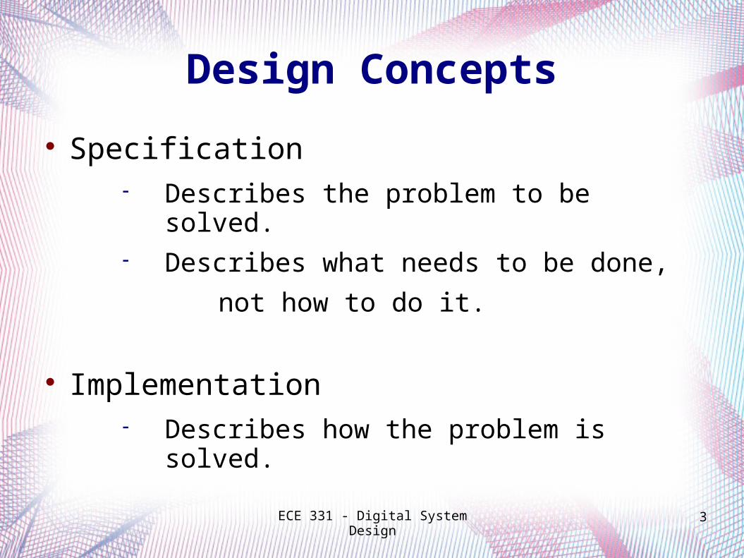
Design Concepts
Specification Describes the problem to be solved. Describes what needs to be done,
not how to do it.
Implementation Describes how the problem is solved.
ECE 331 - Digital System Design 4
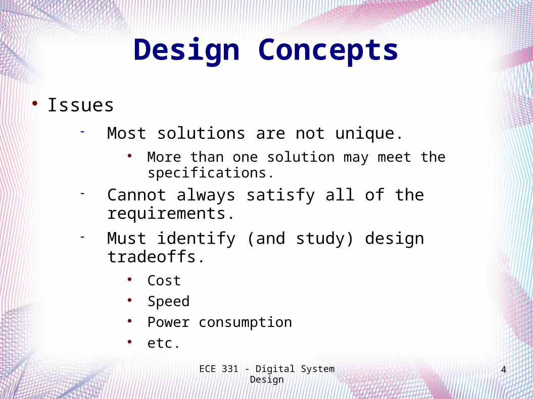
Design Concepts
Issues Most solutions are not unique.
More than one solution may meet the specifications.
Cannot always satisfy all of the requirements. Must identify (and study) design tradeoffs.
Cost Speed Power consumption etc.
ECE 331 - Digital System Design 5
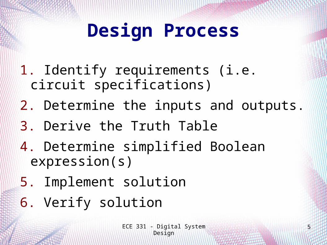
Design Process
1. Identify requirements (i.e. circuit specifications)
2. Determine the inputs and outputs.
3. Derive the Truth Table
4. Determine simplified Boolean expression(s)
5. Implement solution
6. Verify solution

ECE 331 - Digital System Design 6
Exercise:
Design a combinational logic circuit to meet the following specifications:
1. 3-bit input (A = a2a
1a
0)
2. 1-bit output (z)3. Output is high (logic 1) when 2 < A <= 5.

ECE 331 - Digital System Design 7
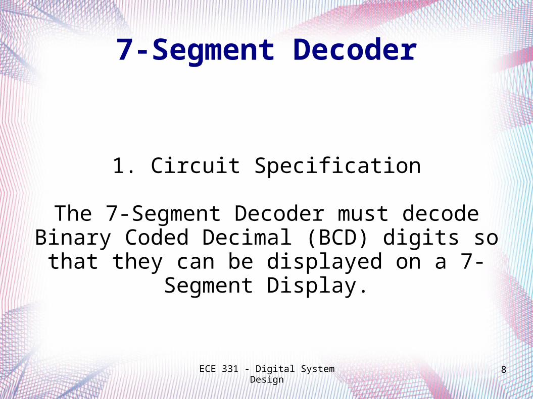
Example:
Design a 7-Segment Decoder
ECE 331 - Digital System Design 8
1. Circuit Specification
The 7-Segment Decoder must decode Binary Coded Decimal (BCD) digits so that they can be
displayed on a 7-Segment Display.
7-Segment Decoder

ECE 331 - Digital System Design 9
2. Determine Inputs and Outputs
Input: Binary Coded Decimal digits
7-Segment Decoder

ECE 331 - Digital System Design 10
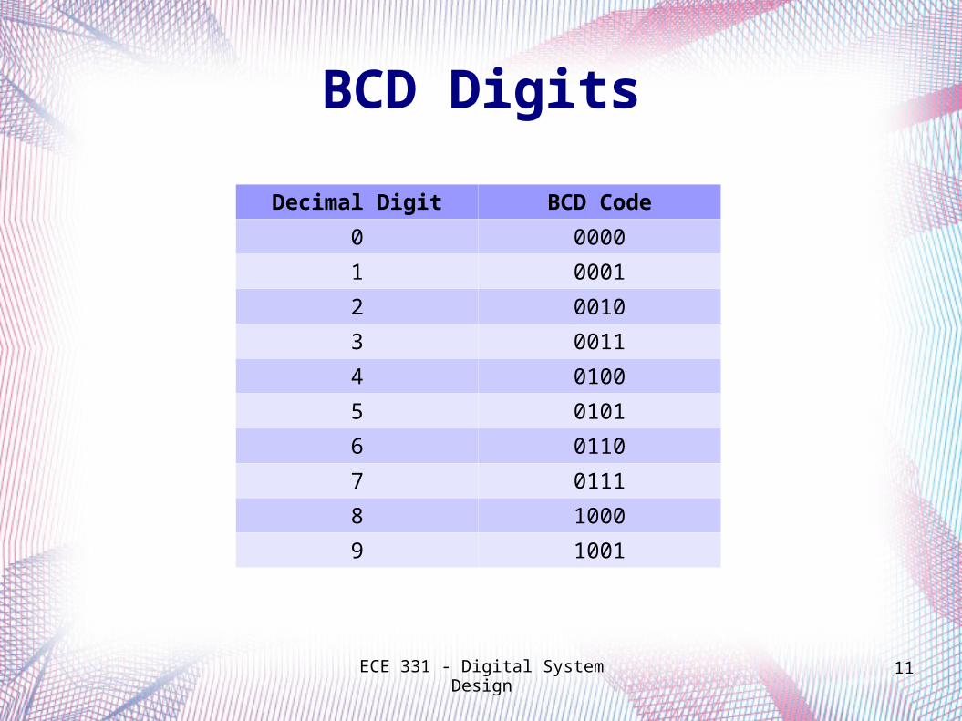
Binary Coded Decimal
Assign a 4-bit code to each decimal digit. A 4-bit code can represent 16 values. There are only 10 digits in the decimal number
system. Unassigned codes are not used.
How do we interpret these unused codes? Hint: think about K-maps.
ECE 331 - Digital System Design 11
BCD Digits
Decimal Digit BCD Code
0 0000
1 0001
2 0010
3 0011
4 0100
5 0101
6 0110
7 0111
8 1000
9 1001

ECE 331 - Digital System Design 12
2. Determine Inputs and Outputs
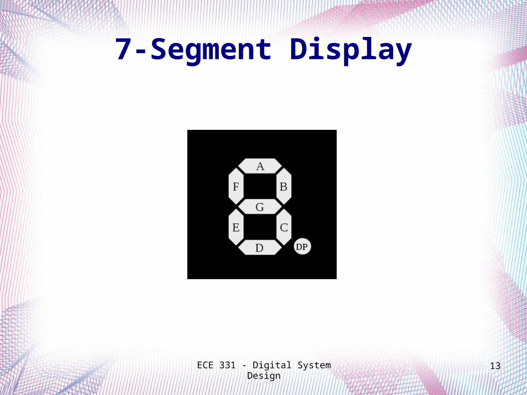
Output: 7-Segment Display
7-Segment Decoder
ECE 331 - Digital System Design 13
7-Segment Display

ECE 331 - Digital System Design 14
7-Segment Display

ECE 331 - Digital System Design 15
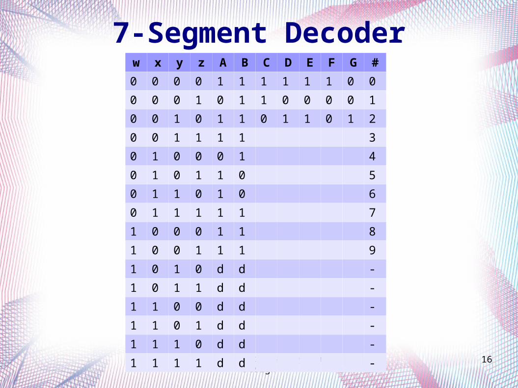
3. Derive Truth Table
7-Segment Decoder
ECE 331 - Digital System Design 16
7-Segment Decoderw x y z A B C D E F G #
0 0 0 0 1 1 1 1 1 1 0 0
0 0 0 1 0 1 1 0 0 0 0 1
0 0 1 0 1 1 0 1 1 0 1 2
0 0 1 1 1 1 3
0 1 0 0 0 1 4
0 1 0 1 1 0 5
0 1 1 0 1 0 6
0 1 1 1 1 1 7
1 0 0 0 1 1 8
1 0 0 1 1 1 9
1 0 1 0 d d -
1 0 1 1 d d -
1 1 0 0 d d -
1 1 0 1 d d -
1 1 1 0 d d -
1 1 1 1 d d -

ECE 331 - Digital System Design 17
4. Determine simplified Boolean expression(s)
7-Segment Decoder
ECE 331 - Digital System Design 18
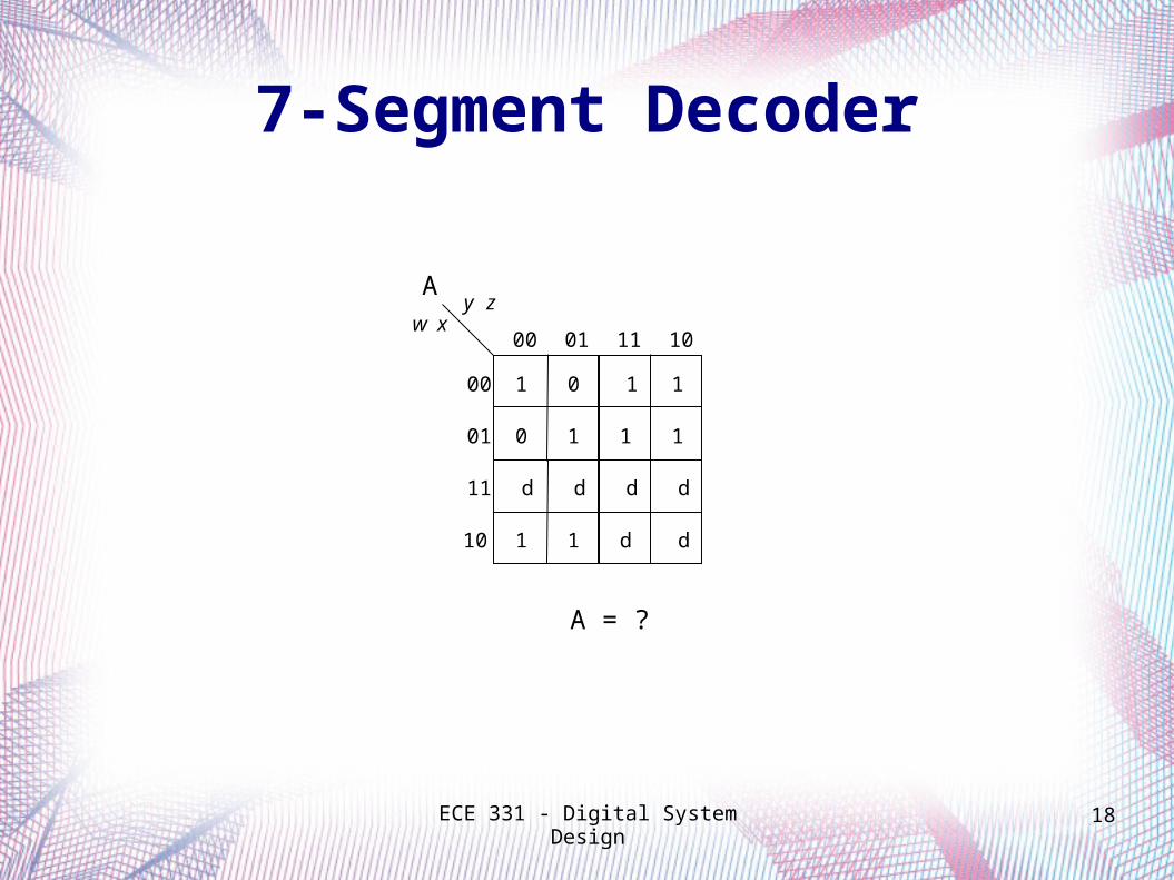
7-Segment Decoder
y z w x
1
00 01 11 10
0 1 1
0 1 1 1
d d d d
1 1 d d
00
01
11
10
A
A = ?

ECE 331 - Digital System Design 19
7-Segment Decoder
y z w x
1
00 01 11 10
1 1 1
1 0 1 0
d d d d
1 1 d d
00
01
11
10
B
B = ?

ECE 331 - Digital System Design 20
Student Exercise:
Determine the minimized Boolean expression for each of the segments of the 7-Segment Display.
7-Segment Decoder
ECE 331 - Digital System Design 21
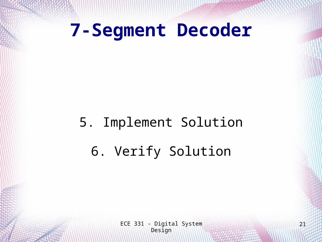
5. Implement Solution
6. Verify Solution
7-Segment Decoder

ECE 331 - Digital System Design 22
Multiple-Output Logic Circuits
ECE 331 - Digital System Design 23
Example:
Given two functions, F1 and F
2, of the same input
variables x1.. x
4, design the minimum-cost
implementation.
Multiple-Output Logic Circuits

ECE 331 - Digital System Design 24
x 1 x 2 x 3 x 4 00 01 11 10
1 1
1 1
1 1
1 1
00
01
11
10
(a) Function
1
f 1
x 1 x 2 x 3 x 4 00 01 11 10
1 1
1 1
1 1 1
1 1
00
01
11
10
(b) Function f 2
F1 = X1'.X3 + X1.X3' + X2.X3'.X4 F1 = X1'.X3 + X1.X3' + X2.X3.X4
Multiple-Output Logic Circuits

ECE 331 - Digital System Design 25
f 1
f 2
x 2
x 3
x 4
x 1
x 3
x 1
x 3
x 2
x 3
x 4
(c) Combined circuit for f 1 f 2 and
Multiple-Output Logic Circuits

ECE 331 - Digital System Design 26
Example:
Given two functions, F3 and F
4, of the same input
variables x1.. x
4, design the minimum-cost
implementation for the combined circuit.
Note: the minimum-cost implementation for the combined circuit may notbe the same as the minimum-cost implementations for the individual circuits.
Multiple-Output Logic Circuits

ECE 331 - Digital System Design 27
x 1 x 2 x 3 x 4 00 01 11 10
1
1 1
1
00
01
11
10
(a) Optimal realization of (b) Optimal realization of
1
f 3 f 4
1
1
x 1 x 2 x 3 x 4 00 01 11 10
1 1
1
1
00
01
11
10
1
1 1
F3 = X1'.X4 + X2.X4 + X1'.X2.X3 F3 = X2'.X4 + X1.X4 + X1'.X2.X3.X4'
Logic Gates required: 2 2-input AND 1 3-input AND 1 3-input OR
Logic Gates required: 2 2-input AND 1 4-input AND 1 3-input OR
Total Gates and Inputs required: 8 Logic Gates 21 Inputs
Multiple-Output Logic Circuits
ECE 331 - Digital System Design 28
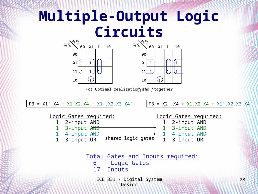
(c) Optimal realization of f 3
x 1 x 2 x 3 x 4 00 01 11 10
1
1 1
1
00
01
11
10
1 1
1
x 1 x 2 x 3 x 4 00 01 11 10
1 1
1
1
00
01
11
10
1
1 1
and togetherf 4
F3 = X1'.X4 + X1.X2.X4 + X1'.X2.X3.X4' F3 = X2'.X4 + X1.X2.X4 + X1'.X2.X3.X4'
Logic Gates required: 1 2-input AND 1 3-input AND 1 4-input AND 1 3-input OR
Logic Gates required: 1 2-input AND 1 3-input AND 1 4-input AND 1 3-input OR
Total Gates and Inputs required: 6 Logic Gates 17 Inputs
shared logic gates
Multiple-Output Logic Circuits
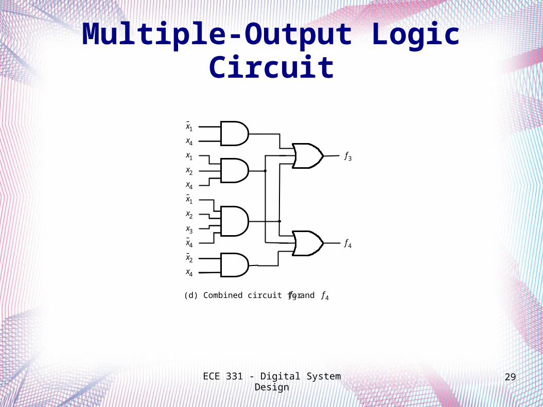
ECE 331 - Digital System Design 29
f 3
f 4
x 1
x 4
x 3
x 4
x 1
x 1
x 2
x 2
x 4
x 4
(d) Combined circuit for f 3 f 4 and
x 2
Multiple-Output Logic Circuit