dspic30f flash programming specificationww1.microchip.com/downloads/en/devicedoc/70102k.pdf ·...
TRANSCRIPT
dsPIC30FdsPIC30F Flash Programming Specification
1.0 OVERVIEW AND SCOPEThis document defines the programming specification for the dsPIC30F family of Digital Signal Controllers (DSCs). The programming specification is required only for the developers of third-party tools that are used to program dsPIC30F devices. Customers using dsPIC30F devices should use development tools that already provide support for device programming.
This document includes programming specifications for the following devices:
• dsPIC30F2010/2011/2012• dsPIC30F3010/3011/3012/3013/ 3014• dsPIC30F4011/4012/4013• dsPIC30F5011/5013/5015/5016• dsPIC30F6010/6011/6012/6013/6014/6015• dsPIC30F6010A/6011A/6012A/6013A/6014A
2.0 PROGRAMMING OVERVIEW OF THE dsPIC30F
The dsPIC30F family of DSCs contains a region of on-chip memory used to simplify device programming. This region of memory can store a programming executive, which allows the dsPIC30F to be programmed faster than the traditional means. Once the programming executive is stored to memory by an external programmer (such as Microchip’s MPLAB®
ICD 2, MPLAB PM3, PRO MATE® II, or MPLAB REAL ICE™), it can then interact with the external programmer to efficiently program devices.
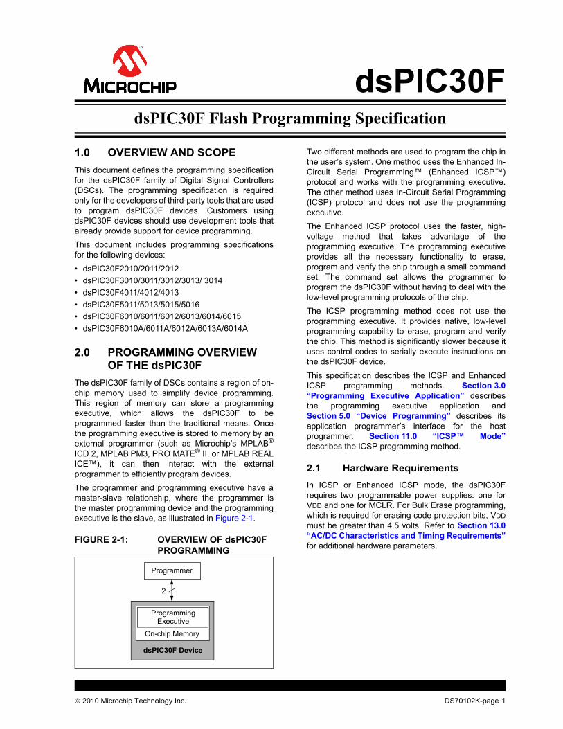
The programmer and programming executive have a master-slave relationship, where the programmer is the master programming device and the programming executive is the slave, as illustrated in Figure 2-1.
FIGURE 2-1: OVERVIEW OF dsPIC30F PROGRAMMING
Two different methods are used to program the chip in the user’s system. One method uses the Enhanced In-Circuit Serial Programming™ (Enhanced ICSP™) protocol and works with the programming executive. The other method uses In-Circuit Serial Programming (ICSP) protocol and does not use the programming executive.
The Enhanced ICSP protocol uses the faster, high-voltage method that takes advantage of the programming executive. The programming executive provides all the necessary functionality to erase, program and verify the chip through a small command set. The command set allows the programmer to program the dsPIC30F without having to deal with the low-level programming protocols of the chip.
The ICSP programming method does not use the programming executive. It provides native, low-level programming capability to erase, program and verify the chip. This method is significantly slower because it uses control codes to serially execute instructions on the dsPIC30F device.
This specification describes the ICSP and Enhanced ICSP programming methods. Section 3.0 “Programming Executive Application” describes the programming executive application and Section 5.0 “Device Programming” describes its application programmer’s interface for the host programmer. Section 11.0 “ICSP™ Mode”describes the ICSP programming method.
2.1 Hardware RequirementsIn ICSP or Enhanced ICSP mode, the dsPIC30Frequires two programmable power supplies: one for VDD and one for MCLR. For Bulk Erase programming, which is required for erasing code protection bits, VDDmust be greater than 4.5 volts. Refer to Section 13.0 “AC/DC Characteristics and Timing Requirements”for additional hardware parameters.
Programmer
dsPIC30F Device
ProgrammingExecutive
On-chip Memory
2
© 2010 Microchip Technology Inc. DS70102K-page 1
dsPIC30F Flash Programming Specification
2.2 Pins Used During ProgrammingThe pins identified in Table 2-1 are used for device programming. Refer to the appropriate device data sheet for complete pin descriptions.
TABLE 2-1: dsPIC30F PIN DESCRIPTIONS DURING PROGRAMMING
Pin Name Pin Type Pin Description
MCLR/VPP P Programming Enable
VDD P Power Supply
VSS P Ground
PGC I Serial Clock
PGD I/O Serial Data
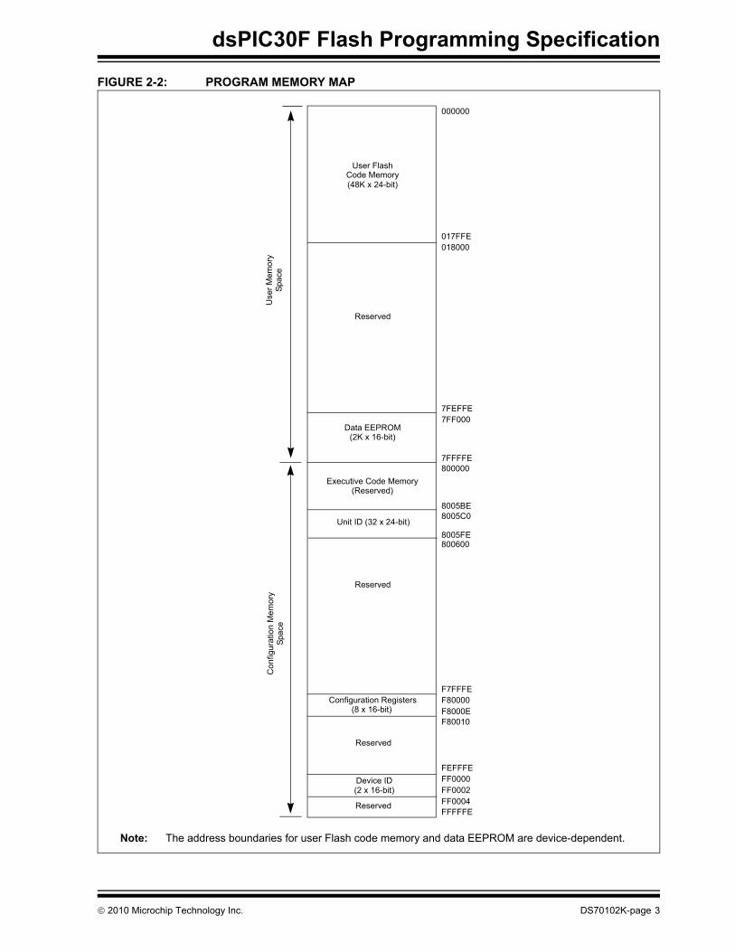
2.3 Program Memory MapThe program memory space extends from 0x0 to 0xFFFFFE. Code storage is located at the base of the memory map and supports up to 144 Kbytes (48K instruction words). Code is stored in three, 48 Kbyte memory panels that reside on-chip. Table 2-2 shows the location and program memory size of each device.
Locations 0x800000 through 0x8005BE are reserved for executive code memory. This region stores either the programming executive or debugging executive. The programming executive is used for device programming, while the debug executive is used for in-circuit debugging. This region of memory cannot be used to store user code.
Locations 0xF80000 through 0xF8000E are reserved for the Configuration registers. The bits in these registers may be set to select various device options, and are described in Section 5.7 “Configuration Bits Programming”.
Locations 0xFF0000 and 0xFF0002 are reserved for the Device ID registers. These bits can be used by the programmer to identify what device type is being programmed and are described in Section 10.0 “Device ID”. The device ID reads out normally, even after code protection is applied.
Figure 2-2 illustrates the memory map for the dsPIC30F devices.
2.4 Data EEPROM MemoryThe Data EEPROM array supports up to 4 Kbytes of data and is located in one memory panel. It is mapped in program memory space, residing at the end of User Memory Space (see Figure 2-2). Table 2-2 shows the location and size of data EEPROM in each device.
TABLE 2-2: CODE MEMORY AND DATA EEPROM MAP AND SIZE
Device Code Memory map(Size in Instruction Words)
Data EEPROM Memory Map(Size in Bytes)
dsPIC30F2010 0x000000-0x001FFE (4K) 0x7FFC00-0x7FFFFE (1K)dsPIC30F2011 0x000000-0x001FFE (4K) None (0K)dsPIC30F2012 0x000000-0x001FFE (4K) None (0K)dsPIC30F3010 0x000000-0x003FFE (8K) 0x7FFC00-0x7FFFFE (1K)dsPIC30F3011 0x000000-0x003FFE (8K) 0x7FFC00-0x7FFFFE (1K)dsPIC30F3012 0x000000-0x003FFE (8K) 0x7FFC00-0x7FFFFE (1K)dsPIC30F3013 0x000000-0x003FFE (8K) 0x7FFC00-0x7FFFFE (1K)dsPIC30F3014 0x000000-0x003FFE (8K) 0x7FFC00-0x7FFFFE (1K)dsPIC30F4011 0x000000-0x007FFE (16K) 0x7FFC00-0x7FFFFE (1K)dsPIC30F4012 0x000000-0x007FFE (16K) 0x7FFC00-0x7FFFFE (1K)dsPIC30F4013 0x000000-0x007FFE (16K) 0x7FFC00-0x7FFFFE (1K)dsPIC30F5011 0x000000-0x00AFFE (22K) 0x7FFC00-0x7FFFFE (1K)dsPIC30F5013 0x000000-0x00AFFE (22K) 0x7FFC00-0x7FFFFE (1K)dsPIC30F5015 0x000000-0x00AFFE (22K) 0x7FFC00-0x7FFFFE (1K)dsPIC30F5016 0x000000-0x00AFFE (22K) 0x7FFC00-0x7FFFFE (1K)dsPIC30F6010 0x000000-0x017FFE (48K) 0x7FF000-0x7FFFFE (4K)dsPIC30F6010A 0x000000-0x017FFE (48K) 0x7FF000-0x7FFFFF (4K)dsPIC30F6011 0x000000-0x015FFE (44K) 0x7FF800-0x7FFFFE (2K)dsPIC30F6011A 0x000000-0x015FFE (44K) 0x7FF800-0x7FFFFE (2K)dsPIC30F6012 0x000000-0x017FFE (48K) 0x7FF000-0x7FFFFE (4K)dsPIC30F6012A 0x000000-0x017FFE (48K) 0x7FF000-0x7FFFFE (4K)dsPIC30F6013 0x000000-0x015FFE (44K) 0x7FF800-0x7FFFFE (2K)dsPIC30F6013A 0x000000-0x015FFE (44K) 0x7FF800-0x7FFFFE (2K)dsPIC30F6014 0x000000-0x017FFE (48K) 0x7FF000-0x7FFFFE (4K)dsPIC30F6014A 0x000000-0x017FFE (48K) 0x7FF000-0x7FFFFE (4K)dsPIC30F6015 0x000000-0x017FFE (48K) 0x7FF000-0x7FFFFE (4K)
Legend: I = Input, O = Output, P = Power
DS70102K-page 2 © 2010 Microchip Technology Inc.
dsPIC30F Flash Programming Specification
FIGURE 2-2: PROGRAM MEMORY MAP
Use
r Mem
ory
Spac
e
000000
Configuration Registers
User FlashCode Memory
018000017FFE
Con
figur
atio
n M
emor
ySp
ace
Data EEPROM
(48K x 24-bit)
(2K x 16-bit)
800000
F80000(8 x 16-bit) F8000E
F80010
Device IDFEFFFEFF0000
FFFFFE
Reserved
F7FFFE
Reserved
7FF0007FEFFE
8005BE8005C0
Executive Code Memory
7FFFFE
Reserved
FF0002FF0004Reserved
(2 x 16-bit)
(Reserved)
Note: The address boundaries for user Flash code memory and data EEPROM are device-dependent.
Unit ID (32 x 24-bit)8005FE800600
© 2010 Microchip Technology Inc. DS70102K-page 3
dsPIC30F Flash Programming Specification
3.0 PROGRAMMING EXECUTIVE APPLICATION
3.1 Programming Executive OverviewThe programming executive resides in executive memory and is executed when Enhanced ICSP Programming mode is entered. The programming exec-utive provides the mechanism for the programmer (host device) to program and verify the dsPIC30F, using a simple command set and communication protocol.
The following capabilities are provided by the programming executive:
• Read memory- Code memory and data EEPROM- Configuration registers- Device ID
• Erase memory- Bulk Erase by segment- Code memory (by row)- Data EEPROM (by row)
• Program memory- Code memory- Data EEPROM - Configuration registers
• Query- Blank Device- Programming executive software version
The programming executive performs the low-level tasks required for erasing and programming. This allows the programmer to program the device by issuing the appropriate commands and data.
The programming procedure is outlined in Section 5.0 “Device Programming”.
3.2 Programming Executive Code Memory
The programming executive is stored in executive code memory and executes from this reserved region of memory. It requires no resources from user code memory or data EEPROM.
3.3 Programming Executive Data RAMThe programming executive uses the device’s data RAM for variable storage and program execution. Once the programming executive has run, no assumptions should be made about the contents of data RAM.
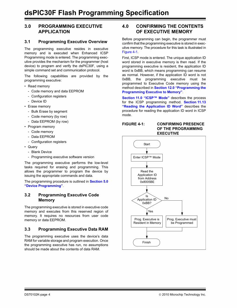
4.0 CONFIRMING THE CONTENTS OF EXECUTIVE MEMORY
Before programming can begin, the programmer must confirm that the programming executive is stored in exec-utive memory. The procedure for this task is illustrated in Figure 4-1.
First, ICSP mode is entered. The unique application ID word stored in executive memory is then read. If the programming executive is resident, the application ID word is 0xBB, which means programming can resume as normal. However, if the application ID word is not 0xBB, the programming executive must be programmed to Executive Code memory using the method described in Section 12.0 “Programming the Programming Executive to Memory”.
Section 11.0 “ICSP™ Mode” describes the process for the ICSP programming method. Section 11.13 “Reading the Application ID Word” describes the procedure for reading the application ID word in ICSP mode.
FIGURE 4-1: CONFIRMING PRESENCE OF THE PROGRAMMING EXECUTIVE
Is
Start
Enter ICSP™ Mode
Application ID0xBB?
Resident in Memory
Yes
No
Prog. Executive is
Application IDRead the
be ProgrammedProg. Executive must
from Address0x8005BE
Finish
DS70102K-page 4 © 2010 Microchip Technology Inc.
dsPIC30F Flash Programming Specification
5.0 DEVICE PROGRAMMING
5.1 Overview of the Programming Process
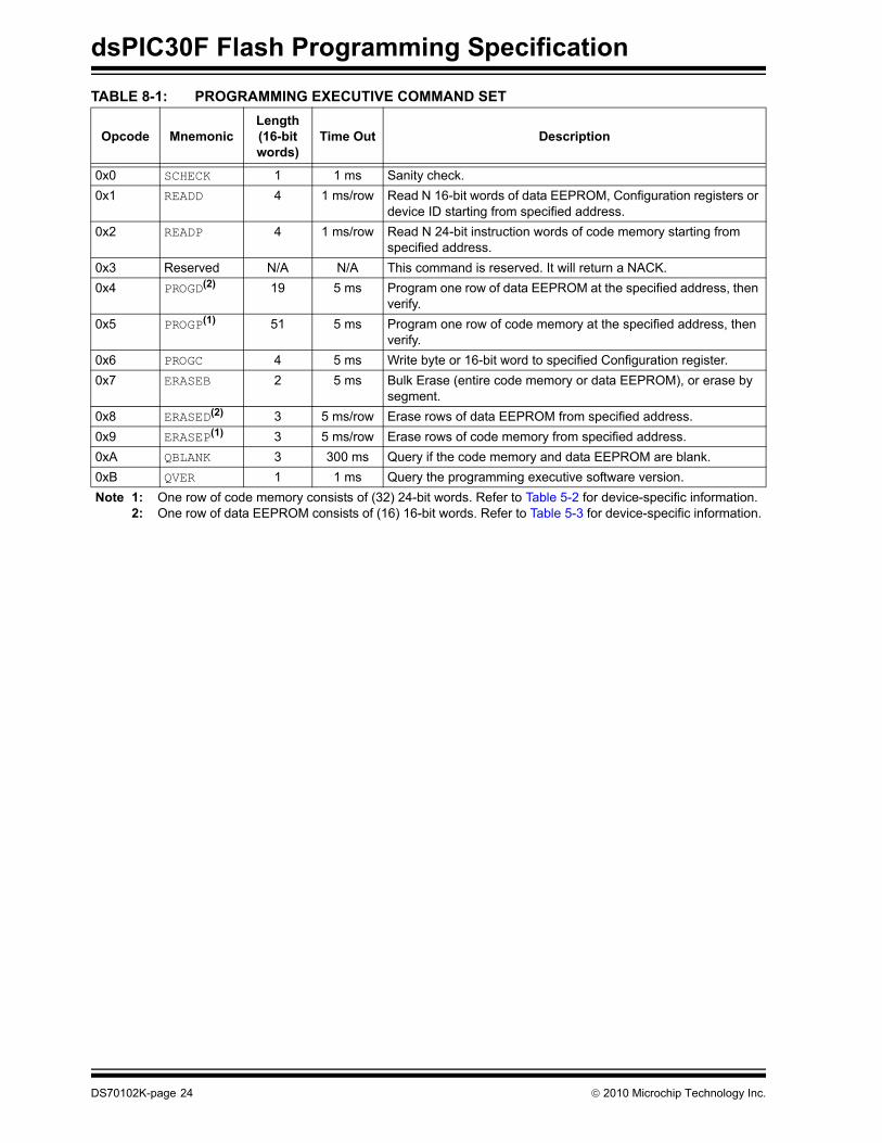
Once the programming executive has been verified in memory (or loaded if not present), the dsPIC30F can be programmed using the command set shown in Table 5-1. A detailed description for each command is provided in Section 8.0 “Programming Executive Commands”.
TABLE 5-1: COMMAND SET SUMMARYCommand Description
SCHECK Sanity checkREADD Read data EEPROM, Configuration
registers and device IDREADP Read code memory PROGD Program one row of data EEPROM
and verifyPROGP Program one row of code memory and
verifyPROGC Program Configuration bits and verifyERASEB Bulk Erase, or erase by segmentERASED Erase data EEPROMERASEP Erase code memoryQBLANK Query if the code memory and data
EEPROM are blankQVER Query the software version
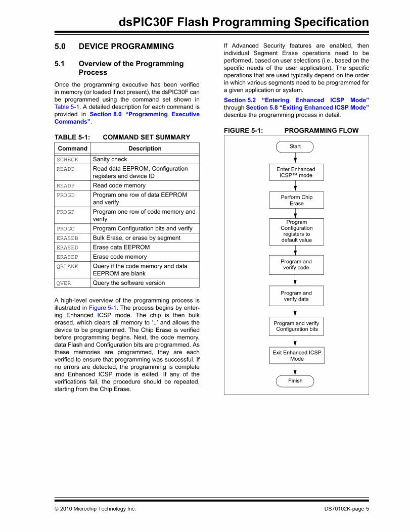
A high-level overview of the programming process is illustrated in Figure 5-1. The process begins by enter-ing Enhanced ICSP mode. The chip is then bulk erased, which clears all memory to ‘1’ and allows the device to be programmed. The Chip Erase is verified before programming begins. Next, the code memory, data Flash and Configuration bits are programmed. As these memories are programmed, they are each verified to ensure that programming was successful. If no errors are detected, the programming is complete and Enhanced ICSP mode is exited. If any of the verifications fail, the procedure should be repeated, starting from the Chip Erase.
If Advanced Security features are enabled, then individual Segment Erase operations need to be performed, based on user selections (i.e., based on the specific needs of the user application). The specific operations that are used typically depend on the order in which various segments need to be programmed for a given application or system.
Section 5.2 “Entering Enhanced ICSP Mode”through Section 5.8 “Exiting Enhanced ICSP Mode”describe the programming process in detail.
FIGURE 5-1: PROGRAMMING FLOW
Start
Program and
Program and
Program and verify Configuration bits
Finish
verify code
verify data
Enter Enhanced
Exit Enhanced ICSPMode
Perform ChipErase
ProgramConfigurationregisters to
ICSP™ mode
default value
© 2010 Microchip Technology Inc. DS70102K-page 5
dsPIC30F Flash Programming Specification
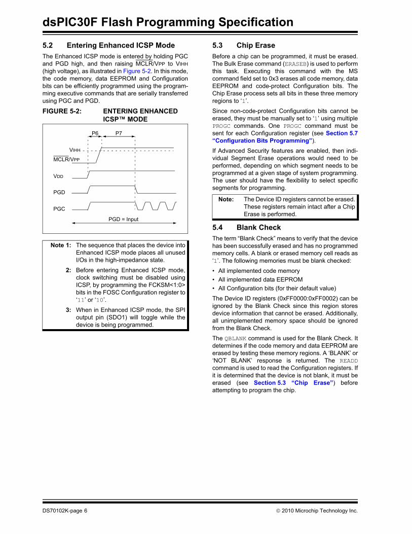
5.2 Entering Enhanced ICSP ModeThe Enhanced ICSP mode is entered by holding PGC and PGD high, and then raising MCLR/VPP to VIHH(high voltage), as illustrated in Figure 5-2. In this mode, the code memory, data EEPROM and Configuration bits can be efficiently programmed using the program-ming executive commands that are serially transferred using PGC and PGD.
FIGURE 5-2: ENTERING ENHANCED ICSP™ MODE
5.3 Chip EraseBefore a chip can be programmed, it must be erased. The Bulk Erase command (ERASEB) is used to perform this task. Executing this command with the MS command field set to 0x3 erases all code memory, data EEPROM and code-protect Configuration bits. The Chip Erase process sets all bits in these three memory regions to ‘1’.
Since non-code-protect Configuration bits cannot be erased, they must be manually set to ‘1’ using multiple PROGC commands. One PROGC command must be sent for each Configuration register (see Section 5.7 “Configuration Bits Programming”).
If Advanced Security features are enabled, then indi-vidual Segment Erase operations would need to be performed, depending on which segment needs to be programmed at a given stage of system programming. The user should have the flexibility to select specific segments for programming.
Note: The Device ID registers cannot be erased. These registers remain intact after a Chip Erase is performed.
5.4 Blank CheckThe term “Blank Check” means to verify that the device has been successfully erased and has no programmed memory cells. A blank or erased memory cell reads as‘1’. The following memories must be blank checked:
• All implemented code memory• All implemented data EEPROM• All Configuration bits (for their default value)
The Device ID registers (0xFF0000:0xFF0002) can be ignored by the Blank Check since this region stores device information that cannot be erased. Additionally, all unimplemented memory space should be ignored from the Blank Check.
The QBLANK command is used for the Blank Check. It determines if the code memory and data EEPROM are erased by testing these memory regions. A ‘BLANK’ or ‘NOT BLANK’ response is returned. The READDcommand is used to read the Configuration registers. If it is determined that the device is not blank, it must be erased (see Section 5.3 “Chip Erase”) before attempting to program the chip.
Note 1: The sequence that places the device into Enhanced ICSP mode places all unused I/Os in the high-impedance state.
2: Before entering Enhanced ICSP mode, clock switching must be disabled using ICSP, by programming the FCKSM<1:0> bits in the FOSC Configuration register to ‘11’ or ‘10’.
3: When in Enhanced ICSP mode, the SPI output pin (SDO1) will toggle while the device is being programmed.
MCLR/VPP
P7
PGD
PGD = Input
PGC
VDD
VIHH
P6
DS70102K-page 6 © 2010 Microchip Technology Inc.
dsPIC30F Flash Programming Specification
5.5 Code Memory Programming5.5.1 OVERVIEWThe Flash code memory array consists of 512 rows of thirty-two, 24-bit instructions. Each panel stores 16K instruction words, and each dsPIC30F device has either 1, 2 or 3 memory panels (see Table 5-2).
TABLE 5-2: DEVICE CODE MEMORY SIZE
DeviceCode Size
(24-bitWords)
Number of
Rows
Number of
Panels
dsPIC30F2010 4K 128 1dsPIC30F2011 4K 128 1dsPIC30F2012 4K 128 1dsPIC30F3010 8K 256 1dsPIC30F3011 8K 256 1dsPIC30F3012 8K 256 1dsPIC30F3013 8K 256 1dsPIC30F3014 8K 256 1dsPIC30F4011 16K 512 1dsPIC30F4012 16K 512 1dsPIC30F4013 16K 512 1dsPIC30F5011 22K 704 2dsPIC30F5013 22K 704 2dsPIC30F5015 22K 704 2dsPIC30F5016 22K 704 2dsPIC30F6010 48K 1536 3dsPIC30F6010A 48K 1536 3dsPIC30F6011 44K 1408 3dsPIC30F6011A 44K 1408 3dsPIC30F6012 48K 1536 3dsPIC30F6012A 48K 1536 3dsPIC30F6013 44K 1408 3dsPIC30F6013A 44K 1408 3dsPIC30F6014 48K 1536 3dsPIC30F6014A 48K 1536 3dsPIC30F6015 48K 1536 3
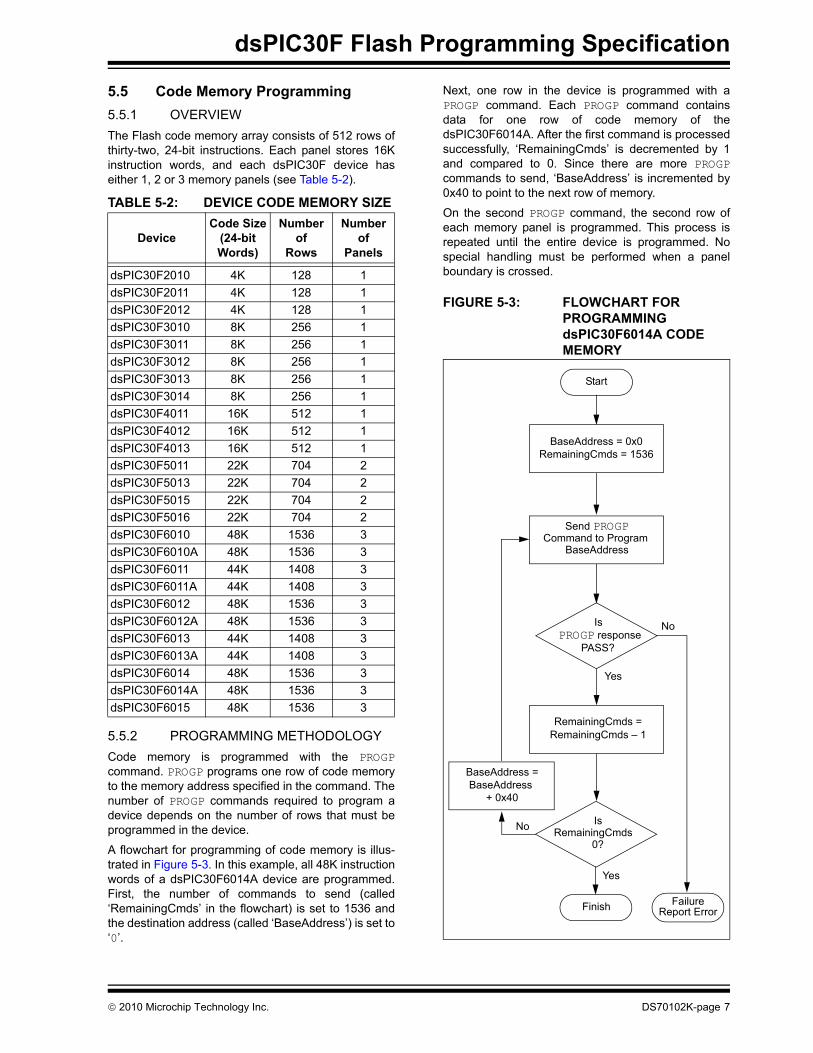
5.5.2 PROGRAMMING METHODOLOGYCode memory is programmed with the PROGPcommand. PROGP programs one row of code memory to the memory address specified in the command. The number of PROGP commands required to program a device depends on the number of rows that must be programmed in the device.
A flowchart for programming of code memory is illus-trated in Figure 5-3. In this example, all 48K instruction words of a dsPIC30F6014A device are programmed. First, the number of commands to send (called ‘RemainingCmds’ in the flowchart) is set to 1536 and the destination address (called ‘BaseAddress’) is set to ‘0’.
Next, one row in the device is programmed with a PROGP command. Each PROGP command contains data for one row of code memory of the dsPIC30F6014A. After the first command is processed successfully, ‘RemainingCmds’ is decremented by 1 and compared to 0. Since there are more PROGPcommands to send, ‘BaseAddress’ is incremented by 0x40 to point to the next row of memory.
On the second PROGP command, the second row of each memory panel is programmed. This process is repeated until the entire device is programmed. No special handling must be performed when a panel boundary is crossed.
FIGURE 5-3: FLOWCHART FOR PROGRAMMING dsPIC30F6014A CODE MEMORY
IsPROGP response
PASS?
IsRemainingCmds
0?
BaseAddress = 0x0RemainingCmds = 1536
RemainingCmds =RemainingCmds – 1
Finish
BaseAddress =BaseAddress
No
No
Yes
Yes
+ 0x40
Start
FailureReport Error
Send PROGPCommand to Program
BaseAddress
© 2010 Microchip Technology Inc. DS70102K-page 7

dsPIC30F Flash Programming Specification
5.5.3 PROGRAMMING VERIFICATIONOnce code memory is programmed, the contents of memory can be verified to ensure that programming was successful. Verification requires code memory to be read back and compared against the copy held in the programmer’s buffer.
The READP command can be used to read back all the programmed code memory.
Alternatively, you can have the programmer perform the verification once the entire device is programmed using a checksum computation, as described in Section 6.8 “Checksum Computation”.
5.6 Data EEPROM Programming
5.6.1 OVERVIEWThe panel architecture for the data EEPROM memory array consists of 128 rows of sixteen 16-bit data words. Each panel stores 2K words. All devices have either one or no memory panels. Devices with data EEPROM provide either 512 words, 1024 words or 2048 words of memory on the one panel (see Table 5-3).
TABLE 5-3: DATA EEPROM SIZE
Device Data EEPROMSize (Words)
Number ofRows
dsPIC30F2010 512 32dsPIC30F2011 0 0dsPIC30F2012 0 0dsPIC30F3010 512 32dsPIC30F3011 512 32dsPIC30F3012 512 32dsPIC30F3013 512 32dsPIC30F3014 512 32dsPIC30F4011 512 32dsPIC30F4012 512 32dsPIC30F4013 512 32dsPIC30F5011 512 32dsPIC30F5013 512 32dsPIC30F5015 512 32dsPIC30F5016 512 32dsPIC30F6010 2048 128dsPIC30F6010A 2048 128dsPIC30F6011 1024 64dsPIC30F6011A 1024 64dsPIC30F6012 2048 128dsPIC30F6012A 2048 128dsPIC30F6013 1024 64dsPIC30F6013A 1024 64dsPIC30F6014 2048 128dsPIC30F6014A 2048 128dsPIC30F6015 2048 128
5.6.2 PROGRAMMING METHODOLOGYThe programming executive uses the PROGD command to program the data EEPROM. Figure 5-4 illustrates the flowchart of the process. Firstly, the number of rows to program (RemainingRows) is based on the device size, and the destination address (DestAddress) is set to ‘0’. In this example, 128 rows (2048 words) of data EEPROM will be programmed.
The first PROGD command programs the first row of data EEPROM. Once the command completes successfully, ‘RemainingRows’ is decremented by 1 and compared with 0. Since there are 127 more rows to program, ‘BaseAddress’ is incremented by 0x20 to point to the next row of data EEPROM. This process is then repeated until all 128 rows of data EEPROM are programmed.
FIGURE 5-4: FLOWCHART FOR PROGRAMMING dsPIC30F6014A DATA EEPROM
IsPROGD response
PASS?
IsRemainingRows
0?
Remaining Rows = 128BaseAddress = 0
RemainingRows =RemainingRows – 1
Finish
BaseAddress =BaseAddress
No
No
Yes
Yes
+ 0x20
Start
Send PROGDCommand with BaseAddress
FailureReport Error
DS70102K-page 8 © 2010 Microchip Technology Inc.
dsPIC30F Flash Programming Specification
5.6.3 PROGRAMMING VERIFICATIONOnce the data EEPROM is programmed, the contents of memory can be verified to ensure that the programming was successful. Verification requires the data EEPROM to be read back and compared against the copy held in the programmer’s buffer. The READDcommand reads back the programmed data EEPROM.
Alternatively, the programmer can perform the verification once the entire device is programmed using a checksum computation, as described in Section 6.8 “Checksum Computation”.
Note: TBLRDL instructions executed within a REPEAT loop must not be used to read from Data EEPROM. Instead, it is recommended to use PSV access.
5.7 Configuration Bits Programming
5.7.1 OVERVIEWThe dsPIC30F has Configuration bits stored in seven 16-bit registers. These bits can be set or cleared to select various device configurations. There are two types of Configuration bits: system-operation bits and code-protect bits. The system-operation bits determine the power-on settings for system-level components such as the oscillator and Watchdog Timer. The code- protect bits prevent program memory from being read and written.
The FOSC Configuration register has three different register descriptions, based on the device. The FOSCConfiguration register description for the dsPIC30F2010 and dsPIC30F6010/6011/6012/6013/6014 devices are shown in Table 5-4.
Note: If user software performs an erase opera-tion on the configuration fuse, it must be followed by a write operation to this fuse with the desired value, even if the desired value is the same as the state of the erased fuse.
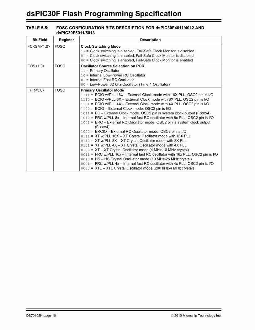
The FOSC Configuration register description for the dsPIC30F4011/4012 and dsPIC30F5011/5013 devices is shown in Table 5-5.
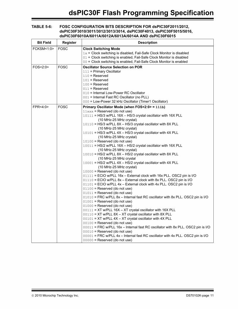
The FOSC Configuration register description for all remaining devices (dsPIC30F2011/2012, dsPIC30F3010/3011/3012/3013, dsPIC30F3014/4013, dsPIC30F5015 and dsPIC30F6011A/6012A/6013A/ 6014A) is shown in Table 5-6. Always use the correct register descriptions for your target processor.
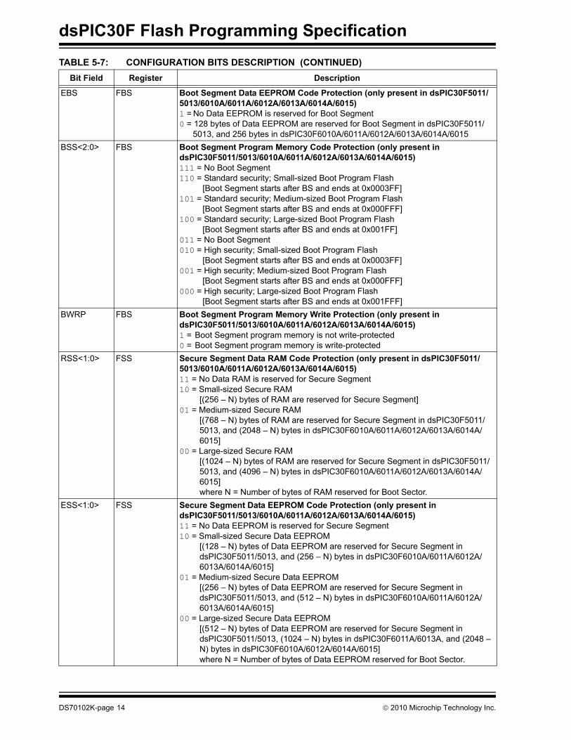
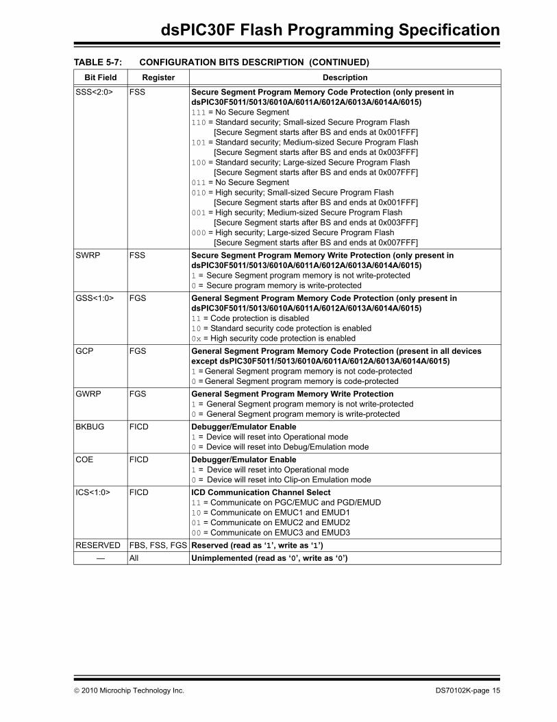
The FWDT, FBORPOR, FBS, FSS, FGS and FICD Configuration registers are not device-dependent. The register descriptions for these Configuration registers are shown in Table 5-7.
The Device Configuration register maps are shown in Table 5-8 through Table 5-11.
TABLE 5-4: FOSC CONFIGURATION BITS DESCRIPTION FOR dsPIC30F2010 AND dsPIC30F6010/6011/6012/6013/6014
Bit Field Register Description
FCKSM<1:0> FOSC Clock Switching Mode 1x = Clock switching is disabled, Fail-Safe Clock Monitor is disabled01 = Clock switching is enabled, Fail-Safe Clock Monitor is disabled00 = Clock switching is enabled, Fail-Safe Clock Monitor is enabled
FOS<1:0> FOSC Oscillator Source Selection on POR 11 = Primary Oscillator10 = Internal Low-Power RC Oscillator01 = Internal Fast RC Oscillator00 = Low-Power 32 kHz Oscillator (Timer1 Oscillator)
FPR<3:0> FOSC Primary Oscillator Mode 1111 = ECIO w/PLL 16X – External Clock mode with 16X PLL. OSC2 pin is I/O1110 = ECIO w/PLL 8X – External Clock mode with 8X PLL. OSC2 pin is I/O1101 = ECIO w/PLL 4X – External Clock mode with 4X PLL. OSC2 pin is I/O1100 = ECIO – External Clock mode. OSC2 pin is I/O1011 = EC – External Clock mode. OSC2 pin is system clock output (FOSC/4)1010 = Reserved (do not use)1001 = ERC – External RC Oscillator mode. OSC2 pin is system clock output
(FOSC/4)1000 = ERCIO – External RC Oscillator mode. OSC2 pin is I/O0111 = XT w/PLL 16X – XT Crystal Oscillator mode with 16X PLL0110 = XT w/PLL 8X – XT Crystal Oscillator mode with 8X PLL0101 = XT w/PLL 4X – XT Crystal Oscillator mode with 4X PLL0100 = XT – XT Crystal Oscillator mode (4 MHz-10 MHz crystal)001x = HS – HS Crystal Oscillator mode (10 MHz-25 MHz crystal)000x = XTL – XTL Crystal Oscillator mode (200 kHz-4 MHz crystal)
© 2010 Microchip Technology Inc. DS70102K-page 9
dsPIC30F Flash Programming Specification
TABLE 5-5: FOSC CONFIGURATION BITS DESCRIPTION FOR dsPIC30F4011/4012 AND dsPIC30F5011/5013
Bit Field Register Description
FCKSM<1:0> FOSC Clock Switching Mode 1x = Clock switching is disabled, Fail-Safe Clock Monitor is disabled01 = Clock switching is enabled, Fail-Safe Clock Monitor is disabled00 = Clock switching is enabled, Fail-Safe Clock Monitor is enabled
FOS<1:0> FOSC Oscillator Source Selection on POR
FPR<3:0> FOSC Primary Oscillator Mode 1111 = ECIO w/PLL 16X – External Clock mode with 16X PLL. OSC2 pin is I/O1110 = ECIO w/PLL 8X – External Clock mode with 8X PLL. OSC2 pin is I/O1101 = ECIO w/PLL 4X – External Clock mode with 4X PLL. OSC2 pin is I/O1100 = ECIO – External Clock mode. OSC2 pin is I/O1011 = EC – External Clock mode. OSC2 pin is system clock output (FOSC/4)1010 = FRC w/PLL 8x – Internal fast RC oscillator with 8x PLL. OSC2 pin is I/O1001 = ERC – External RC Oscillator mode. OSC2 pin is system clock output
(FOSC/4)1000 = ERCIO – External RC Oscillator mode. OSC2 pin is I/O0111 = XT w/PLL 16X – XT Crystal Oscillator mode with 16X PLL0110 = XT w/PLL 8X – XT Crystal Oscillator mode with 8X PLL 0101 = XT w/PLL 4X – XT Crystal Oscillator mode with 4X PLL 0100 = XT – XT Crystal Oscillator mode (4 MHz-10 MHz crystal)0011 = FRC w/PLL 16x – Internal fast RC oscillator with 16x PLL. OSC2 pin is I/O0010 = HS – HS Crystal Oscillator mode (10 MHz-25 MHz crystal)0001 = FRC w/PLL 4x – Internal fast RC oscillator with 4x PLL. OSC2 pin is I/O0000 = XTL – XTL Crystal Oscillator mode (200 kHz-4 MHz crystal)
11 = Primary Oscillator10 = Internal Low-Power RC Oscillator01 = Internal Fast RC Oscillator00 = Low-Power 32 kHz Oscillator (Timer1 Oscillator)
DS70102K-page 10 © 2010 Microchip Technology Inc.
dsPIC30F Flash Programming Specification
TABLE 5-6: FOSC CONFIGURATION BITS DESCRIPTION FOR dsPIC30F2011/2012, dsPIC30F3010/3011/3012/3013/3014, dsPIC30F4013, dsPIC30F5015/5016, dsPIC30F6010A/6011A/6012A/6013A/6014A AND dsPIC30F6015
Bit Field Register Description
FCKSM<1:0> FOSC Clock Switching Mode 1x = Clock switching is disabled, Fail-Safe Clock Monitor is disabled01 = Clock switching is enabled, Fail-Safe Clock Monitor is disabled00 = Clock switching is enabled, Fail-Safe Clock Monitor is enabled
FOS<2:0> FOSC Oscillator Source Selection on POR 111 = Primary Oscillator110 = Reserved101 = Reserved100 = Reserved011 = Reserved010 = Internal Low-Power RC Oscillator001 = Internal Fast RC Oscillator (no PLL)000 = Low-Power 32 kHz Oscillator (Timer1 Oscillator)
FPR<4:0> FOSC Primary Oscillator Mode (when FOS<2:0> = 111b) 11xxx = Reserved (do not use) 10111 = HS/3 w/PLL 16X – HS/3 crystal oscillator with 16X PLL
(10 MHz-25 MHz crystal) 10110 = HS/3 w/PLL 8X – HS/3 crystal oscillator with 8X PLL
(10 MHz-25 MHz crystal) 10101 = HS/3 w/PLL 4X – HS/3 crystal oscillator with 4X PLL
(10 MHz-25 MHz crystal) 10100 = Reserved (do not use) 10011 = HS/2 w/PLL 16X – HS/2 crystal oscillator with 16X PLL
(10 MHz-25 MHz crystal) 10010 = HS/2 w/PLL 8X – HS/2 crystal oscillator with 8X PLL
(10 MHz-25 MHz crystal 10001 = HS/2 w/PLL 4X – HS/2 crystal oscillator with 4X PLL
(10 MHz-25 MHz crystal) 10000 = Reserved (do not use) 01111 = ECIO w/PLL 16x – External clock with 16x PLL. OSC2 pin is I/O 01110 = ECIO w/PLL 8x – External clock with 8x PLL. OSC2 pin is I/O 01101 = ECIO w/PLL 4x – External clock with 4x PLL. OSC2 pin is I/O 01100 = Reserved (do not use) 01011 = Reserved (do not use) 01010 = FRC w/PLL 8x – Internal fast RC oscillator with 8x PLL. OSC2 pin is I/O 01001 = Reserved (do not use) 01000 = Reserved (do not use) 00111 = XT w/PLL 16X – XT crystal oscillator with 16X PLL 00110 = XT w/PLL 8X – XT crystal oscillator with 8X PLL 00101 = XT w/PLL 4X – XT crystal oscillator with 4X PLL 00100 = Reserved (do not use) 00011 = FRC w/PLL 16x – Internal fast RC oscillator with 8x PLL. OSC2 pin is I/O 00010 = Reserved (do not use) 00001 = FRC w/PLL 4x – Internal fast RC oscillator with 4x PLL. OSC2 pin is I/O 00000 = Reserved (do not use)
© 2010 Microchip Technology Inc. DS70102K-page 11

dsPIC30F Flash Programming Specification
FPR<4:0> FOSC Alternate Oscillator Mode (when FOS<2:0> = 011b) 1xxxx = Reserved (do not use) 0111x = Reserved (do not use) 01101 = Reserved (do not use) 01100 = ECIO – External clock. OSC2 pin is I/O 01011 = EC – External clock. OSC2 pin is system clock output (FOSc/4) 01010 = Reserved (do not use) 01001 = ERC – External RC oscillator. OSC2 pin is system clock output (FOSC/4) 01000 = ERCIO – External RC oscillator. OSC2 pin is I/O 00111 = Reserved (do not use) 00110 = Reserved (do not use) 00101 = Reserved (do not use) 00100 = XT – XT crystal oscillator (4 MHz-10 MHz crystal) 00010 = HS – HS crystal oscillator (10 MHz-25 MHz crystal) 00001 = Reserved (do not use) 00000 = XTL – XTL crystal oscillator (200 kHz-4 MHz crystal)
TABLE 5-6: FOSC CONFIGURATION BITS DESCRIPTION FOR dsPIC30F2011/2012, dsPIC30F3010/3011/3012/3013/3014, dsPIC30F4013, dsPIC30F5015/5016, dsPIC30F6010A/6011A/6012A/6013A/6014A AND dsPIC30F6015 (CONTINUED)
Bit Field Register Description
DS70102K-page 12 © 2010 Microchip Technology Inc.

dsPIC30F Flash Programming Specification
TABLE 5-7: CONFIGURATION BITS DESCRIPTION Bit Field Register Description
FWPSA<1:0> FWDT Watchdog Timer Prescaler A11 = 1:51210 = 1:6401 = 1:800 = 1:1
FWPSB<3:0> FWDT Watchdog Timer Prescaler B1111 = 1:161110 = 1:15
•••
0001 = 1:20000 = 1:1
FWDTEN FWDT Watchdog Enable1 = Watchdog enabled (LPRC oscillator cannot be disabled. Clearing the SWDTEN
bit in the RCON register will have no effect)0 = Watchdog disabled (LPRC oscillator can be disabled by clearing the SWDTEN bit
in the RCON register)MCLREN FBORPOR Master Clear Enable
1 = Master Clear pin (MCLR) is enabled0 = MCLR pin is disabled
PWMPIN FBORPOR Motor Control PWM Module Pin Mode1 = PWM module pins controlled by PORT register at device Reset (tri-stated)0 = PWM module pins controlled by PWM module at device Reset (configured as out-
put pins)HPOL FBORPOR Motor Control PWM Module High-Side Polarity
1 = PWM module high-side output pins have active-high output polarity 0 = PWM module high-side output pins have active-low output polarity
LPOL FBORPOR Motor Control PWM Module Low-Side Polarity1 = PWM module low-side output pins have active-high output polarity 0 = PWM module low-side output pins have active-low output polarity
BOREN FBORPOR PBOR Enable1 = PBOR enabled 0 = PBOR disabled
BORV<1:0> FBORPOR Brown-out Voltage Select11 = 2.0V (not a valid operating selection)10 = 2.7V01 = 4.2V00 = 4.5V
FPWRT<1:0> FBORPOR Power-on Reset Timer Value Select11 = PWRT = 64 ms10 = PWRT = 16 ms01 = PWRT = 4 ms00 = Power-up Timer disabled
RBS<1:0> FBS Boot Segment Data RAM Code Protection (only present in dsPIC30F5011/5013/6010A/6011A/6012A/6013A/6014A/6015)11 = No Data RAM is reserved for Boot Segment10 = Small-sized Boot RAM
[128 bytes of RAM are reserved for Boot Segment]01 = Medium-sized Boot RAM
[256 bytes of RAM are reserved for Boot Segment]00 = Large-sized Boot RAM
[512 bytes of RAM are reserved for Boot Segment in dsPIC30F5011/5013, and 1024 bytes in dsPIC30F6010A/6011A/6012A/6013A/6014A/6015]
© 2010 Microchip Technology Inc. DS70102K-page 13
dsPIC30F Flash Programming Specification
EBS FBS Boot Segment Data EEPROM Code Protection (only present in dsPIC30F5011/5013/6010A/6011A/6012A/6013A/6014A/6015)1 = No Data EEPROM is reserved for Boot Segment0 = 128 bytes of Data EEPROM are reserved for Boot Segment in dsPIC30F5011/
5013, and 256 bytes in dsPIC30F6010A/6011A/6012A/6013A/6014A/6015 BSS<2:0> FBS Boot Segment Program Memory Code Protection (only present in
dsPIC30F5011/5013/6010A/6011A/6012A/6013A/6014A/6015)111 = No Boot Segment110 = Standard security; Small-sized Boot Program Flash
[Boot Segment starts after BS and ends at 0x0003FF]101 = Standard security; Medium-sized Boot Program Flash
[Boot Segment starts after BS and ends at 0x000FFF]100 = Standard security; Large-sized Boot Program Flash
[Boot Segment starts after BS and ends at 0x001FF]011 = No Boot Segment010 = High security; Small-sized Boot Program Flash
[Boot Segment starts after BS and ends at 0x0003FF]001 = High security; Medium-sized Boot Program Flash
[Boot Segment starts after BS and ends at 0x000FFF]000 = High security; Large-sized Boot Program Flash
[Boot Segment starts after BS and ends at 0x001FFF]BWRP FBS Boot Segment Program Memory Write Protection (only present in
dsPIC30F5011/5013/6010A/6011A/6012A/6013A/6014A/6015) 1 = Boot Segment program memory is not write-protected0 = Boot Segment program memory is write-protected
RSS<1:0> FSS Secure Segment Data RAM Code Protection (only present in dsPIC30F5011/5013/6010A/6011A/6012A/6013A/6014A/6015)11 = No Data RAM is reserved for Secure Segment10 = Small-sized Secure RAM
[(256 – N) bytes of RAM are reserved for Secure Segment]01 = Medium-sized Secure RAM
[(768 – N) bytes of RAM are reserved for Secure Segment in dsPIC30F5011/5013, and (2048 – N) bytes in dsPIC30F6010A/6011A/6012A/6013A/6014A/6015]
00 = Large-sized Secure RAM[(1024 – N) bytes of RAM are reserved for Secure Segment in dsPIC30F5011/5013, and (4096 – N) bytes in dsPIC30F6010A/6011A/6012A/6013A/6014A/6015]where N = Number of bytes of RAM reserved for Boot Sector.
ESS<1:0> FSS Secure Segment Data EEPROM Code Protection (only present in dsPIC30F5011/5013/6010A/6011A/6012A/6013A/6014A/6015)11 = No Data EEPROM is reserved for Secure Segment10 = Small-sized Secure Data EEPROM
[(128 – N) bytes of Data EEPROM are reserved for Secure Segment in dsPIC30F5011/5013, and (256 – N) bytes in dsPIC30F6010A/6011A/6012A/6013A/6014A/6015]
01 = Medium-sized Secure Data EEPROM[(256 – N) bytes of Data EEPROM are reserved for Secure Segment in dsPIC30F5011/5013, and (512 – N) bytes in dsPIC30F6010A/6011A/6012A/6013A/6014A/6015]
00 = Large-sized Secure Data EEPROM[(512 – N) bytes of Data EEPROM are reserved for Secure Segment in dsPIC30F5011/5013, (1024 – N) bytes in dsPIC30F6011A/6013A, and (2048 – N) bytes in dsPIC30F6010A/6012A/6014A/6015]where N = Number of bytes of Data EEPROM reserved for Boot Sector.
TABLE 5-7: CONFIGURATION BITS DESCRIPTION (CONTINUED)Bit Field Register Description
DS70102K-page 14 © 2010 Microchip Technology Inc.
dsPIC30F Flash Programming Specification
SSS<2:0> FSS Secure Segment Program Memory Code Protection (only present in dsPIC30F5011/5013/6010A/6011A/6012A/6013A/6014A/6015)111 = No Secure Segment110 = Standard security; Small-sized Secure Program Flash
[Secure Segment starts after BS and ends at 0x001FFF]101 = Standard security; Medium-sized Secure Program Flash
[Secure Segment starts after BS and ends at 0x003FFF]100 = Standard security; Large-sized Secure Program Flash
[Secure Segment starts after BS and ends at 0x007FFF]011 = No Secure Segment010 = High security; Small-sized Secure Program Flash
[Secure Segment starts after BS and ends at 0x001FFF]001 = High security; Medium-sized Secure Program Flash
[Secure Segment starts after BS and ends at 0x003FFF]000 = High security; Large-sized Secure Program Flash
[Secure Segment starts after BS and ends at 0x007FFF]SWRP FSS Secure Segment Program Memory Write Protection (only present in
dsPIC30F5011/5013/6010A/6011A/6012A/6013A/6014A/6015) 1 = Secure Segment program memory is not write-protected0 = Secure program memory is write-protected
GSS<1:0> FGS General Segment Program Memory Code Protection (only present in dsPIC30F5011/5013/6010A/6011A/6012A/6013A/6014A/6015)11 = Code protection is disabled10 = Standard security code protection is enabled0x = High security code protection is enabled
GCP FGS General Segment Program Memory Code Protection (present in all devices except dsPIC30F5011/5013/6010A/6011A/6012A/6013A/6014A/6015)1 = General Segment program memory is not code-protected0 = General Segment program memory is code-protected
GWRP FGS General Segment Program Memory Write Protection 1 = General Segment program memory is not write-protected0 = General Segment program memory is write-protected
BKBUG FICD Debugger/Emulator Enable1 = Device will reset into Operational mode0 = Device will reset into Debug/Emulation mode
COE FICD Debugger/Emulator Enable1 = Device will reset into Operational mode0 = Device will reset into Clip-on Emulation mode
ICS<1:0> FICD ICD Communication Channel Select11 = Communicate on PGC/EMUC and PGD/EMUD 10 = Communicate on EMUC1 and EMUD1 01 = Communicate on EMUC2 and EMUD2 00 = Communicate on EMUC3 and EMUD3
RESERVED FBS, FSS, FGS Reserved (read as ‘1’, write as ‘1’)— All Unimplemented (read as ‘0’, write as ‘0’)
TABLE 5-7: CONFIGURATION BITS DESCRIPTION (CONTINUED)Bit Field Register Description
© 2010 Microchip Technology Inc. DS70102K-page 15
dsPIC30F Flash Program
ming Specification
DS
70102K-page 16
© 2010 M
icrochip Technology Inc.
D dsPIC30F6010/ 6011/6012/6013/
Bit 4 Bit 3 Bit 2 Bit 1 Bit 0
— FPR<3:0>
SA<1:0> FWPSB<3:0>
V<1:0> — — FPWRT<1:0>
— Reserved(2)
— Reserved(2)
— — Reserved(2) GCP GWRP
— — — ICS<1:0>
Bit 4 Bit 3 Bit 2 Bit 1 Bit 0
— FPR<3:0>
SA<1:0> FWPSB<3:0>
V<1:0> — — FPWRT<1:0>
— BSS<2:0>
— SSS<2:0>
— — GSS<1:0> GWRP
— — — ICS<1:0>
BWRP
SWRP
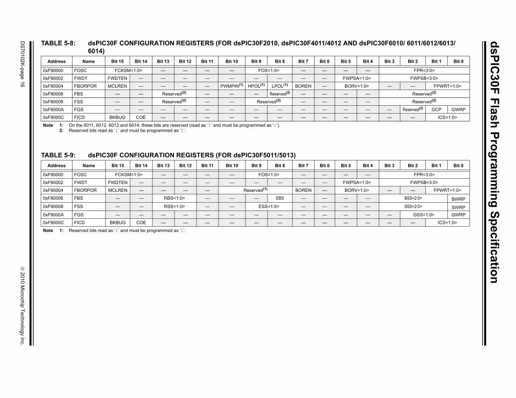
TABLE 5-8: dsPIC30F CONFIGURATION REGISTERS (FOR dsPIC30F2010, dsPIC30F4011/4012 AN6014)
Address Name Bit 15 Bit 14 Bit 13 Bit 12 Bit 11 Bit 10 Bit 9 Bit 8 Bit 7 Bit 6 Bit 5
0xF80000 FOSC FCKSM<1:0> — — — — FOS<1:0> — — —
0xF80002 FWDT FWDTEN — — — — — — — — — FWP
0xF80004 FBORPOR MCLREN — — — — PWMPIN(1) HPOL(1) LPOL(1) BOREN — BOR
0xF80006 FBS — — Reserved(2) — — — Reserved(2) — — —
0xF80008 FSS — — Reserved(2) — — Reserved(2) — — —
0xF8000A FGS — — — — — — — — — — —
0xF8000C FICD BKBUG COE — — — — — — — — —
Note 1: On the 6011, 6012, 6013 and 6014, these bits are reserved (read as ‘1’ and must be programmed as ‘1’).2: Reserved bits read as ‘1’ and must be programmed as ‘1’.
TABLE 5-9: dsPIC30F CONFIGURATION REGISTERS (FOR dsPIC30F5011/5013) Address Name Bit 15 Bit 14 Bit 13 Bit 12 Bit 11 Bit 10 Bit 9 Bit 8 Bit 7 Bit 6 Bit 5
0xF80000 FOSC FCKSM<1:0> — — — — FOS<1:0> — — —
0xF80002 FWDT FWDTEN — — — — — — — — — FWP
0xF80004 FBORPOR MCLREN — — — — Reserved(1) BOREN — BOR
0xF80006 FBS — — RBS<1:0> — — — EBS — — —
0xF80008 FSS — — RSS<1:0> — — ESS<1:0> — — —
0xF8000A FGS — — — — — — — — — — —
0xF8000C FICD BKBUG COE — — — — — — — — —
Note 1: Reserved bits read as ‘1’ and must be programmed as ‘1’.

© 2010 M
icrochip Technology Inc.D
S70102K
-page 17
dsPIC30F Flash Program
ming Specification
TA 12/3013/3014, dsPIC30F4013 AND
Bit 4 Bit 3 Bit 2 Bit 1 Bit 0
0x FPR<4:0>
0x :0> FWPSB<3:0>
0x 0> — — FPWRT<1:0>
0x — Reserved(2)
0x — Reserved(2)
0x — — Reserved(3) GCP GWRP
0x — — — ICS<1:0>
No
TA AND dsPIC30F6015)Bit 4 Bit 3 Bit 2 Bit 1 Bit 0
0x FPR<4:0>
0x :0> FWPSB<3:0>
0x 0> — — FPWRT<1:0>
0x — BSS<2:0>
0x — SSS<2:0>
0x — — GSS<1:0> GWRP
0x — — — ICS<1:0>
No
BWRP
SWRP
BLE 5-10: dsPIC30F CONFIGURATION REGISTERS (FOR dsPIC30F2011/2012, dsPIC30F3010/3011/30dsPIC30F5015/5016)
Address Name Bit 15 Bit 14 Bit 13 Bit 12 Bit 11 Bit 10 Bit 9 Bit 8 Bit 7 Bit 6 Bit 5
F80000 FOSC FCKSM<1:0> — — — FOS<2:0> — — —
F80002 FWDT FWDTEN — — — — — — — — — FWPSA<1
F80004 FBORPOR MCLREN — — — — PWMPIN(1) HPOL(1) LPOL(1) BOREN — BORV<1:
F80006 FBS — — Reserved(2) — — — Reserved(2) — — —
F80008 FSS — — Reserved(2) — — Reserved(2) — — —
F8000A FGS — — — — — — — — — — —
F8000C FICD BKBUG COE — — — — — — — — —
te 1: On the 2011, 2012, 3012, 3013, 3014 and 4013, these bits are reserved (read as ‘1’ and must be programmed as ‘1’).2: Reserved bits read as ‘1’ and must be programmed as ‘1’.3: The FGS<2> bit is a read-only copy of the GCP bit (FGS<1>).
BLE 5-11: dsPIC30F CONFIGURATION REGISTERS (FOR dsPIC30F6010A/6011A/6012A/6013A/6014AAddress Name Bit 15 Bit 14 Bit 13 Bit 12 Bit 11 Bit 10 Bit 9 Bit 8 Bit 7 Bit 6 Bit 5
F80000 FOSC FCKSM<1:0> — — — FOS<2:0> — — —
F80002 FWDT FWDTEN — — — — — — — — — FWPSA<1
F80004 FBORPOR MCLREN — — — — PWMPIN(1) HPOL(1) LPOL(1) BOREN — BORV<1:
F80006 FBS — — RBS<1:0> — — — EBS — — —
F80008 FSS — — RSS<1:0> — — ESS<1:0> — — —
F8000A FGS — — — — — — — — — — —
F8000C FICD BKBUG COE — — — — — — — — —
te 1: On the 6011A, 6012A, 6013A and 6014A, these bits are reserved (read as ‘1’ and must be programmed as ‘1’).
dsPIC30F Flash Programming Specification
5.7.2 PROGRAMMING METHODOLOGYSystem operation Configuration bits are inherently different than all other memory cells. Unlike code memory, data EEPROM and code-protect Configuration bits, the system operation bits cannot be erased. If the chip is erased with the ERASEBcommand, the system-operation bits retain their previous value. Consequently, you should make no assumption about the value of the system operation bits. They should always be programmed to their desired setting.
Configuration bits are programmed as a single word at a time using the PROGC command. The PROGCcommand specifies the configuration data and Configuration register address. When Configuration bits are programmed, any unimplemented bits must be programmed with a ‘0’, and any reserved bits must be programmed with a ‘1’.
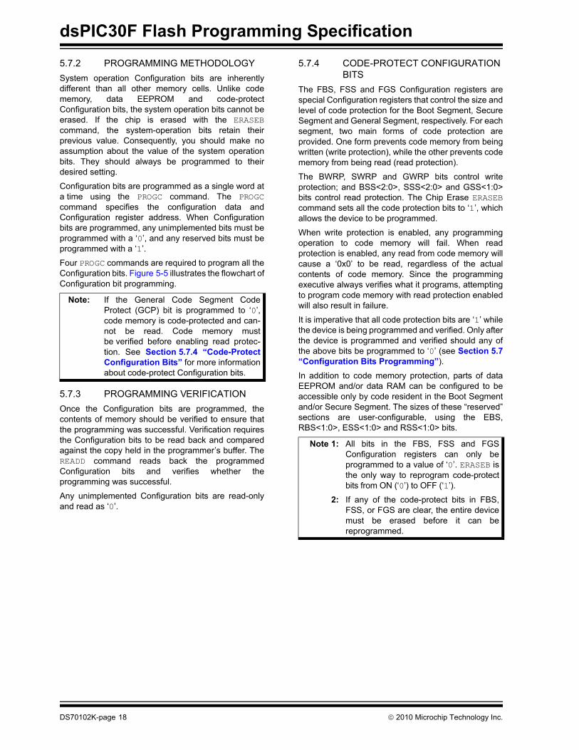
Four PROGC commands are required to program all the Configuration bits. Figure 5-5 illustrates the flowchart of Configuration bit programming.
Note: If the General Code Segment Code Protect (GCP) bit is programmed to ‘0’, code memory is code-protected and can-not be read. Code memory must be verified before enabling read protec-tion. See Section 5.7.4 “Code-Protect Configuration Bits” for more information about code-protect Configuration bits.
5.7.3 PROGRAMMING VERIFICATIONOnce the Configuration bits are programmed, the contents of memory should be verified to ensure that the programming was successful. Verification requires the Configuration bits to be read back and compared against the copy held in the programmer’s buffer. The READD command reads back the programmed Configuration bits and verifies whether the programming was successful.
Any unimplemented Configuration bits are read-only and read as ‘0’.
5.7.4 CODE-PROTECT CONFIGURATION BITS
The FBS, FSS and FGS Configuration registers are special Configuration registers that control the size and level of code protection for the Boot Segment, Secure Segment and General Segment, respectively. For each segment, two main forms of code protection are provided. One form prevents code memory from being written (write protection), while the other prevents code memory from being read (read protection).
The BWRP, SWRP and GWRP bits control write protection; and BSS<2:0>, SSS<2:0> and GSS<1:0> bits control read protection. The Chip Erase ERASEBcommand sets all the code protection bits to ‘1’, which allows the device to be programmed.
When write protection is enabled, any programming operation to code memory will fail. When read protection is enabled, any read from code memory will cause a ‘0x0’ to be read, regardless of the actual contents of code memory. Since the programming executive always verifies what it programs, attempting to program code memory with read protection enabled will also result in failure.
It is imperative that all code protection bits are ‘1’ while the device is being programmed and verified. Only after the device is programmed and verified should any of the above bits be programmed to ‘0’ (see Section 5.7 “Configuration Bits Programming”).
In addition to code memory protection, parts of data EEPROM and/or data RAM can be configured to be accessible only by code resident in the Boot Segment and/or Secure Segment. The sizes of these “reserved” sections are user-configurable, using the EBS, RBS<1:0>, ESS<1:0> and RSS<1:0> bits.
Note 1: All bits in the FBS, FSS and FGS Configuration registers can only be programmed to a value of ‘0’. ERASEB is the only way to reprogram code-protect bits from ON (‘0’) to OFF (‘1’).
2: If any of the code-protect bits in FBS, FSS, or FGS are clear, the entire device must be erased before it can be reprogrammed.
DS70102K-page 18 © 2010 Microchip Technology Inc.
dsPIC30F Flash Programming Specification
5.8 Exiting Enhanced ICSP ModeThe Enhanced ICSP mode is exited by removing power from the device or bringing MCLR to VIL. When normal user mode is next entered, the program that was stored using Enhanced ICSP will execute.
FIGURE 5-5: CONFIGURATION BIT PROGRAMMING FLOW
Send PROGCCommand
ConfigAddress = 0xF80000
IsPROGC Response
PASS?
No
Yes
No
FailureReport Error
Start
Finish
Yes
IsConfigAddress
0xF8000C?
ConfigAddress =ConfigAddress + 2
© 2010 Microchip Technology Inc. DS70102K-page 19
dsPIC30F Flash Programming Specification
6.0 OTHER PROGRAMMING FEATURES
6.1 Erasing MemoryMemory is erased by using an ERASEB, ERASED or ERASEP command, as detailed in Section 8.5 “Command Descriptions”. Code memory can be erased by row using ERASEP. Data EEPROM can be erased by row using ERASED. When memory is erased, the affected memory locations are set to ‘1’s.
ERASEB provides several Bulk Erase options. Performing a Chip Erase with the ERASEB command clears all code memory, data EEPROM and code protection registers. Alternatively, ERASEB can be used to selectively erase either all code memory or data EEPROM. Erase options are summarized in Table 6-1.
TABLE 6-1: ERASE OPTIONS Command Affected Region
ERASEB Entire chip(1) or all code memory or all data EEPROM, or erase by segment
ERASED Specified rows of data EEPROMERASEP(2) Specified rows of code memoryNote 1: The system operation Configuration
registers and device ID registers are not erasable.
2: ERASEP cannot be used to erase code-protect Configuration bits. These bits must be erased using ERASEB.
6.2 Modifying MemoryInstead of bulk-erasing the device before programming, it is possible that you may want to modify only a section of an already programmed device. In this situation, Chip Erase is not a realistic option.
Instead, you can erase selective rows of code memory and data EEPROM using ERASEP and ERASED, respectively. You can then reprogram the modified rows with the PROGP and PROGD command pairs. In these cases, when code memory is programmed, single-panel programming must be specified in the PROGP command.
For modification of Advanced Code Protection bits for a particular segment, the entire chip must first be erased with the ERASEB command. Alternatively, on devices that support Advanced Security, individual segments (code and/or data EEPROM) may be erased, by suitably changing the MS (Memory Select)
field in the ERASEB command. The code-protect Configuration bits can then be reprogrammed using the PROGC command.
Note: If read or write code protection is enabled for a segment, no modifications can be made to that segment until code protection is disabled. Code protection can only be disabled by performing a Chip Erase or by performing a Segment Erase operation for the required segment.
6.3 Reading MemoryThe READD command reads the data EEPROM, Configuration bits and device ID of the device. This command only returns 16-bit data and operates on 16-bit registers. READD can be used to return the entire contents of data EEPROM.
The READP command reads the code memory of the device. This command only returns 24-bit data packed as described in Section 8.3 “Packed Data Format”. READP can be used to read up to 32K instruction words of code memory.
Note: Reading an unimplemented memory location causes the programming executive to reset. All READD and READPcommands must specify only valid memory locations.
6.4 Programming Executive Software Version
At times, it may be necessary to determine the version of programming executive stored in executive memory. The QVER command performs this function. See Section 8.5.11 “QVER Command” for more details about this command.
6.5 Data EEPROM Information in the Hexadecimal File
To allow portability of code, the programmer must read the data EEPROM information from the hexadecimal file. If data EEPROM information is not present, a simple warning message should be issued by the programmer. Similarly, when saving a hexadecimal file, all data EEPROM information must be included. An option to not include the data EEPROM information can be provided.
Microchip Technology Inc. believes that this feature is important for the benefit of the end customer.
DS70102K-page 20 © 2010 Microchip Technology Inc.
dsPIC30F Flash Programming Specification
6.6 Configuration Information in the Hexadecimal File
To allow portability of code, the programmer must read the Configuration register locations from the hexadecimal file. If configuration information is not present in the hexadecimal file, a simple warning message should be issued by the programmer. Similarly, while saving a hexadecimal file, all configuration information must be included. An option to not include the configuration information can be provided.
Microchip Technology Inc. feels strongly that this feature is important for the benefit of the end customer.
6.7 Unit IDThe dsPIC30F devices contain 32 instructions of Unit ID. These are located at addresses 0x8005C0 through 0x8005FF. The Unit ID can be used for storing product information such as serial numbers, system manufacturing dates, manufacturing lot numbers and other such application-specific information.
A Bulk Erase does not erase the Unit ID locations. Instead, erase all executive memory using steps 1-4 as shown in Table 12-1, and program the Unit ID along with the programming executive. Alternately, use a Row Erase to erase the row containing the Unit ID locations.
6.8 Checksum ComputationChecksums for the dsPIC30F are 16 bits in size. The checksum is to total sum of the following:
• Contents of code memory locations• Contents of Configuration registers
Table A-1 describes how to calculate the checksum for each device. All memory locations are summed one byte at a time, using only their native data size. More specifically, Configuration and device ID registers are summed by adding the lower two bytes of these locations (the upper byte is ignored), while code memory is summed by adding all three bytes of code memory.
Note: The checksum calculation differs depending on the code-protect setting. Table A-1 describes how to compute the checksum for an unprotected device and a read-protected device. Regardless of the code-protect setting, the Configuration registers can always be read.
7.0 PROGRAMMER – PROGRAMMING EXECUTIVE COMMUNICATION
7.1 Communication OverviewThe programmer and programming executive have a master-slave relationship, where the programmer is the master programming device and the programming executive is the slave.
All communication is initiated by the programmer in the form of a command. Only one command at a time can be sent to the programming executive. In turn, the programming executive only sends one response to the programmer after receiving and processing a command. The programming executive command set is described in Section 8.0 “Programming Executive Commands”. The response set is described in Section 9.0 “Programming Executive Responses”.
7.2 Communication Interface and Protocol
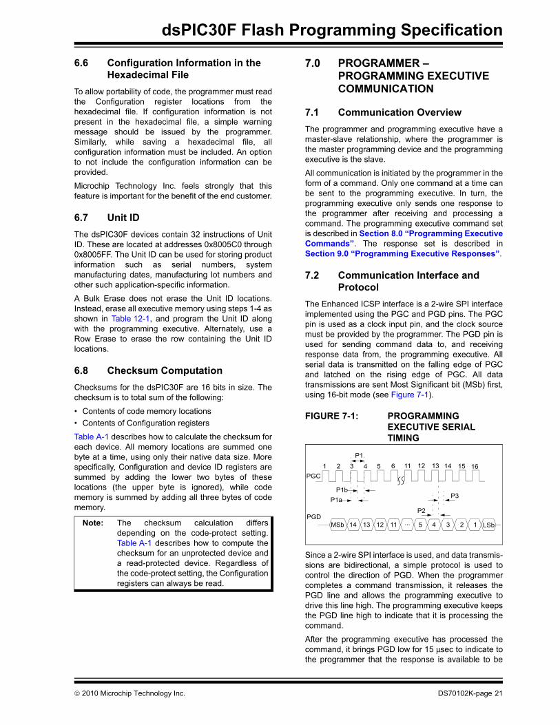
The Enhanced ICSP interface is a 2-wire SPI interface implemented using the PGC and PGD pins. The PGC pin is used as a clock input pin, and the clock source must be provided by the programmer. The PGD pin is used for sending command data to, and receiving response data from, the programming executive. All serial data is transmitted on the falling edge of PGC and latched on the rising edge of PGC. All data transmissions are sent Most Significant bit (MSb) first, using 16-bit mode (see Figure 7-1).
FIGURE 7-1: PROGRAMMING EXECUTIVE SERIAL TIMING
Since a 2-wire SPI interface is used, and data transmis-sions are bidirectional, a simple protocol is used to control the direction of PGD. When the programmer completes a command transmission, it releases the PGD line and allows the programming executive to drive this line high. The programming executive keeps the PGD line high to indicate that it is processing the command.
After the programming executive has processed the command, it brings PGD low for 15 μsec to indicate to the programmer that the response is available to be
PGC
PGD
1 2 3 11 13 15 161412
LSb14 13 12 11
4 5 6
MSb 123... 45
P2
P3
P1
P1aP1b
© 2010 Microchip Technology Inc. DS70102K-page 21
dsPIC30F Flash Programming Specification
clocked out. The programmer can begin to clock out the response 20 μsec after PGD is brought low, and it must provide the necessary amount of clock pulses to receive the entire response from the programming executive.Once the entire response is clocked out, the programmer should terminate the clock on PGC until it is time to send another command to the programming executive. This protocol is illustrated in Figure 7-2.
7.3 SPI RateIn Enhanced ICSP mode, the dsPIC30F operates from the fast internal RC oscillator, which has a nominal frequency of 7.37 MHz. This oscillator frequency yields an effective system clock frequency of 1.84 MHz. Since the SPI module operates in Slave mode, the programmer must limit the SPI clock rate to a frequency no greater than 1 MHz.
Note: If the programmer provides the SPI with a clock faster than 1 MHz, the behavior of the programming executive will be unpredictable.
7.4 Time OutsThe programming executive uses no Watchdog Timer or time out for transmitting responses to the programmer. If the programmer does not follow the flow control mechanism using PGC, as described in Section 7.2 “Communication Interface and Proto-col”, it is possible that the programming executive will behave unexpectedly while trying to send a response to the programmer. Since the programming executive has no time out, it is imperative that the programmer correctly follow the described communication protocol.
As a safety measure, the programmer should use the command time outs identified in Table 8-1. If the command time out expires, the programmer should reset the programming executive and start programming the device again.
FIGURE 7-2: PROGRAMMING EXECUTIVE – PROGRAMMER COMMUNICATION PROTOCOL
1 2 15 16 1 2 15 16
PGC
PGD
PGC = Input PGC = Input (Idle)
Host TransmitsLast Command Word
PGD = Input PGD = Output
P8
1 2 15 16
MSB X X X LSB MSB X X X LSB MSB X X X LSB 1 0
P9b P10
PGC = InputPGD = Output
P9a
Programming ExecutiveProcesses Command Host Clocks Out Response
P11
DS70102K-page 22 © 2010 Microchip Technology Inc.

dsPIC30F Flash Programming Specification
8.0 PROGRAMMING EXECUTIVE COMMANDS
8.1 Command SetThe programming executive command set is shown in Table 8-1. This table contains the opcode, mnemonic, length, time out and description for each command. Functional details on each command are provided in the command descriptions (see Section 8.5 “Command Descriptions”).
8.2 Command FormatAll programming executive commands have a general format consisting of a 16-bit header and any required data for the command (see Figure 8-1). The 16-bit header consists of a 4-bit opcode field, which is used to identify the command, followed by a 12-bit command length field.
FIGURE 8-1: COMMAND FORMAT
The command opcode must match one of those in the command set. Any command that is received which does not match the list in Table 8-1 will return a “NACK” response (see Section 9.2.1 “Opcode Field”).
The command length is represented in 16-bit words since the SPI operates in 16-bit mode. The programming executive uses the Command Length field to determine the number of words to read from the SPI port. If the value of this field is incorrect, the command will not be properly received by the programming executive.
8.3 Packed Data FormatWhen 24-bit instruction words are transferred across the 16-bit SPI interface, they are packed to conserve space using the format shown in Figure 8-2. This format minimizes traffic over the SPI and provides the programming executive with data that is properly aligned for performing table write operations.
Note: When the number of instruction words transferred is odd, MSB2 is zero and lsw2 cannot be transmitted.
FIGURE 8-2: PACKED INSTRUCTION WORD FORMAT
8.4 Programming Executive Error Handling
The programming executive will “NACK” all unsupported commands. Additionally, due to the memory constraints of the programming executive, no checking is performed on the data contained in the Programmer command. It is the responsibility of the programmer to command the programming executive with valid command arguments, or the programming operation may fail. Additional information on error handling is provided in Section 9.2.3 “QE_CodeField”.
15 12 11 0Opcode Length
Command Data First Word (if required)••
Command Data Last Word (if required)
15 8 7 0lsw1
MSB2 MSB1lsw2
lswx: Least significant 16 bits of instruction wordMSBx: Most Significant Byte of instruction word
© 2010 Microchip Technology Inc. DS70102K-page 23
dsPIC30F Flash Programming Specification
TABLE 8-1: PROGRAMMING EXECUTIVE COMMAND SET
Opcode MnemonicLength(16-bitwords)
Time Out Description
0x0 SCHECK 1 1 ms Sanity check.0x1 READD 4 1 ms/row Read N 16-bit words of data EEPROM, Configuration registers or
device ID starting from specified address.0x2 READP 4 1 ms/row Read N 24-bit instruction words of code memory starting from
specified address.0x3 Reserved N/A N/A This command is reserved. It will return a NACK.0x4 PROGD(2) 19 5 ms Program one row of data EEPROM at the specified address, then
verify.0x5 PROGP(1) 51 5 ms Program one row of code memory at the specified address, then
verify. 0x6 PROGC 4 5 ms Write byte or 16-bit word to specified Configuration register.0x7 ERASEB 2 5 ms Bulk Erase (entire code memory or data EEPROM), or erase by
segment.0x8 ERASED(2) 3 5 ms/row Erase rows of data EEPROM from specified address.0x9 ERASEP(1) 3 5 ms/row Erase rows of code memory from specified address.0xA QBLANK 3 300 ms Query if the code memory and data EEPROM are blank.0xB QVER 1 1 ms Query the programming executive software version.Note 1: One row of code memory consists of (32) 24-bit words. Refer to Table 5-2 for device-specific information.
2: One row of data EEPROM consists of (16) 16-bit words. Refer to Table 5-3 for device-specific information.
DS70102K-page 24 © 2010 Microchip Technology Inc.
dsPIC30F Flash Programming Specification
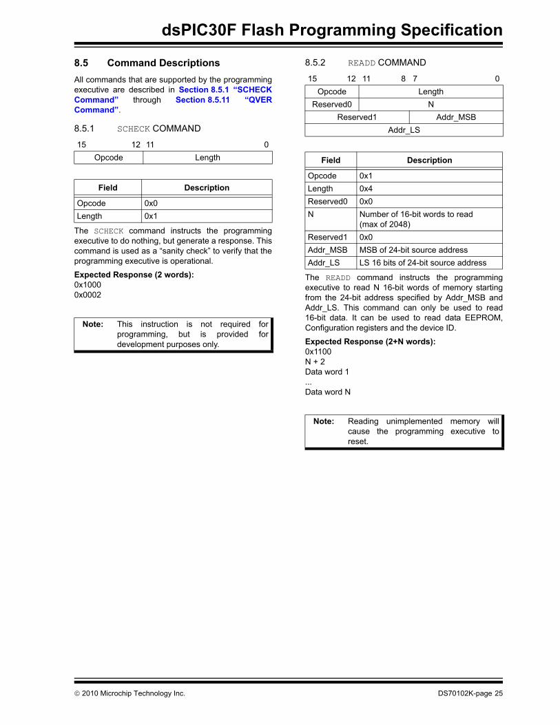
8.5 Command Descriptions All commands that are supported by the programming executive are described in Section 8.5.1 “SCHECKCommand” through Section 8.5.11 “QVERCommand”.
8.5.1 SCHECK COMMAND
15 12 11 0Opcode Length
Field Description
Opcode 0x0Length 0x1
The SCHECK command instructs the programming executive to do nothing, but generate a response. This command is used as a “sanity check” to verify that the programming executive is operational.
Expected Response (2 words): 0x1000 0x0002
Note: This instruction is not required for programming, but is provided for development purposes only.
8.5.2 READD COMMAND
15 12 11 8 7 0Opcode Length
Reserved0 NReserved1 Addr_MSB
Addr_LS
Field Description
Opcode 0x1Length 0x4Reserved0 0x0N Number of 16-bit words to read
(max of 2048)Reserved1 0x0Addr_MSB MSB of 24-bit source addressAddr_LS LS 16 bits of 24-bit source address
The READD command instructs the programming executive to read N 16-bit words of memory starting from the 24-bit address specified by Addr_MSB and Addr_LS. This command can only be used to read 16-bit data. It can be used to read data EEPROM, Configuration registers and the device ID.
Expected Response (2+N words): 0x1100 N + 2 Data word 1 ... Data word N
Note: Reading unimplemented memory will cause the programming executive to reset.
© 2010 Microchip Technology Inc. DS70102K-page 25
dsPIC30F Flash Programming Specification
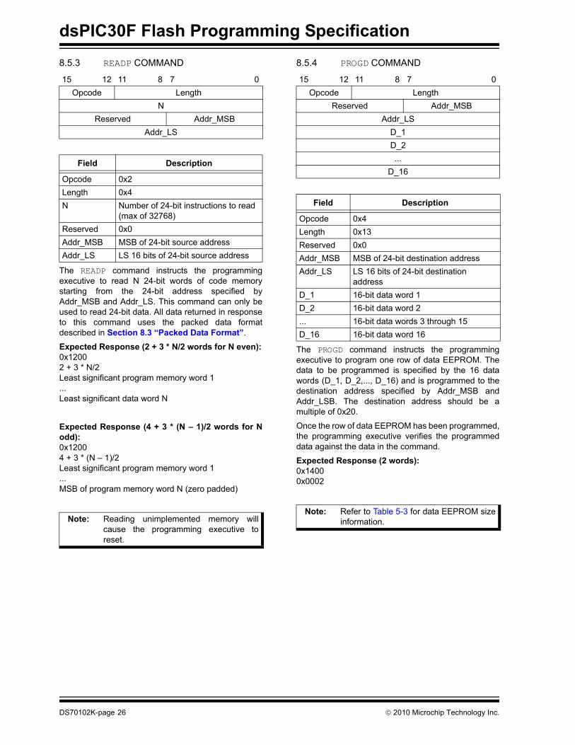
8.5.3 READP COMMAND
15 12 11 8 7 0Opcode Length
NReserved Addr_MSB
Addr_LS
Field Description
Opcode 0x2Length 0x4N Number of 24-bit instructions to read
(max of 32768)Reserved 0x0Addr_MSB MSB of 24-bit source addressAddr_LS LS 16 bits of 24-bit source address
The READP command instructs the programming executive to read N 24-bit words of code memory starting from the 24-bit address specified by Addr_MSB and Addr_LS. This command can only be used to read 24-bit data. All data returned in response to this command uses the packed data format described in Section 8.3 “Packed Data Format”.
Expected Response (2 + 3 * N/2 words for N even): 0x1200 2 + 3 * N/2 Least significant program memory word 1 ... Least significant data word N
Expected Response (4 + 3 * (N – 1)/2 words for N odd): 0x1200 4 + 3 * (N – 1)/2 Least significant program memory word 1 ... MSB of program memory word N (zero padded)
Note: Reading unimplemented memory will cause the programming executive to reset.
8.5.4 PROGD COMMAND
15 12 11 8 7 0Opcode Length
Reserved Addr_MSBAddr_LS
D_1D_2...
D_16
Field Description
Opcode 0x4Length 0x13 Reserved 0x0Addr_MSB MSB of 24-bit destination addressAddr_LS LS 16 bits of 24-bit destination
addressD_1 16-bit data word 1D_2 16-bit data word 2... 16-bit data words 3 through 15D_16 16-bit data word 16
The PROGD command instructs the programming executive to program one row of data EEPROM. The data to be programmed is specified by the 16 data words (D_1, D_2,..., D_16) and is programmed to the destination address specified by Addr_MSB and Addr_LSB. The destination address should be a multiple of 0x20.
Once the row of data EEPROM has been programmed, the programming executive verifies the programmed data against the data in the command.
Expected Response (2 words): 0x1400 0x0002
Note: Refer to Table 5-3 for data EEPROM size information.
DS70102K-page 26 © 2010 Microchip Technology Inc.
dsPIC30F Flash Programming Specification
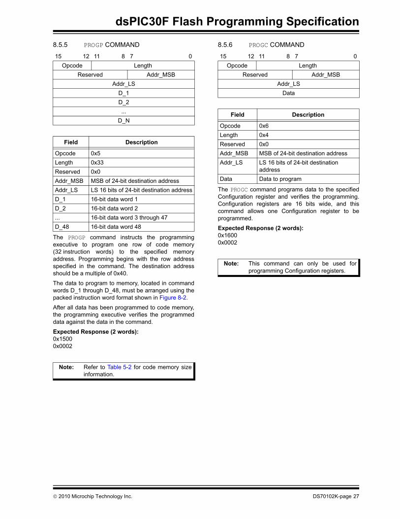
8.5.5 PROGP COMMAND
15 12 11 8 7 0Opcode Length
Reserved Addr_MSBAddr_LS
D_1D_2...
D_N
Field Description
Opcode 0x5Length 0x33Reserved 0x0Addr_MSB MSB of 24-bit destination addressAddr_LS LS 16 bits of 24-bit destination addressD_1 16-bit data word 1D_2 16-bit data word 2... 16-bit data word 3 through 47D_48 16-bit data word 48
The PROGP command instructs the programming executive to program one row of code memory (32 instruction words) to the specified memory address. Programming begins with the row address specified in the command. The destination address should be a multiple of 0x40.
The data to program to memory, located in command words D_1 through D_48, must be arranged using the packed instruction word format shown in Figure 8-2.
After all data has been programmed to code memory, the programming executive verifies the programmed data against the data in the command.
Expected Response (2 words): 0x1500 0x0002
Note: Refer to Table 5-2 for code memory size information.
8.5.6 PROGC COMMAND
15 12 11 8 7 0Opcode Length
Reserved Addr_MSBAddr_LS
Data
Field Description
Opcode 0x6Length 0x4Reserved 0x0Addr_MSB MSB of 24-bit destination addressAddr_LS LS 16 bits of 24-bit destination
addressData Data to program
The PROGC command programs data to the specified Configuration register and verifies the programming. Configuration registers are 16 bits wide, and this command allows one Configuration register to be programmed.
Expected Response (2 words): 0x1600 0x0002
Note: This command can only be used for programming Configuration registers.
© 2010 Microchip Technology Inc. DS70102K-page 27
dsPIC30F Flash Programming Specification
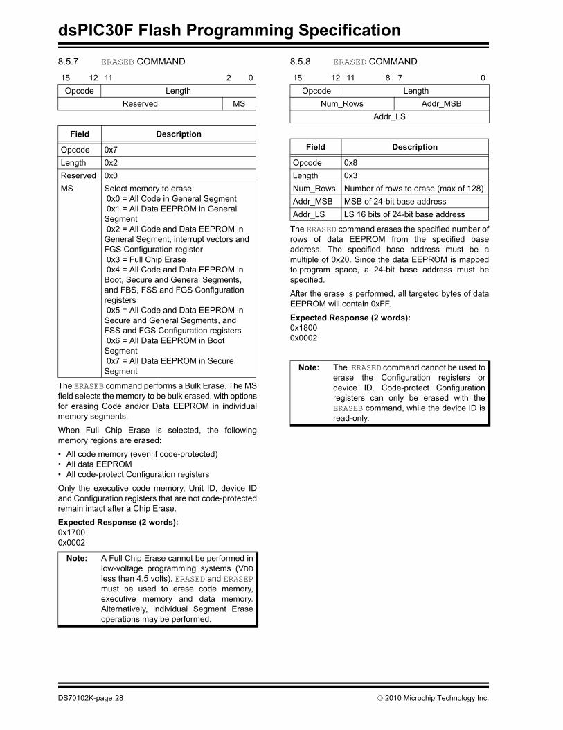
8.5.7 ERASEB COMMAND
15 12 11 2 0Opcode Length
Reserved MS
Field Description
Opcode 0x7Length 0x2Reserved 0x0MS Select memory to erase:
0x0 = All Code in General Segment 0x1 = All Data EEPROM in General Segment 0x2 = All Code and Data EEPROM in General Segment, interrupt vectors and FGS Configuration register 0x3 = Full Chip Erase 0x4 = All Code and Data EEPROM in Boot, Secure and General Segments, and FBS, FSS and FGS Configuration registers 0x5 = All Code and Data EEPROM in Secure and General Segments, and FSS and FGS Configuration registers 0x6 = All Data EEPROM in Boot Segment 0x7 = All Data EEPROM in Secure Segment
The ERASEB command performs a Bulk Erase. The MS field selects the memory to be bulk erased, with options for erasing Code and/or Data EEPROM in individual memory segments.
When Full Chip Erase is selected, the following memory regions are erased:
• All code memory (even if code-protected)• All data EEPROM• All code-protect Configuration registers
Only the executive code memory, Unit ID, device IDand Configuration registers that are not code-protected remain intact after a Chip Erase.
Expected Response (2 words): 0x1700 0x0002
Note: A Full Chip Erase cannot be performed in low-voltage programming systems (VDDless than 4.5 volts). ERASED and ERASEPmust be used to erase code memory, executive memory and data memory. Alternatively, individual Segment Erase operations may be performed.
8.5.8 ERASED COMMAND
15 12 11 8 7 0Opcode Length
Num_Rows Addr_MSBAddr_LS
Field Description
Opcode 0x8Length 0x3Num_Rows Number of rows to erase (max of 128)Addr_MSB MSB of 24-bit base addressAddr_LS LS 16 bits of 24-bit base address
The ERASED command erases the specified number of rows of data EEPROM from the specified base address. The specified base address must be a multiple of 0x20. Since the data EEPROM is mapped to program space, a 24-bit base address must be specified.
After the erase is performed, all targeted bytes of data EEPROM will contain 0xFF.
Expected Response (2 words): 0x1800 0x0002
Note: The ERASED command cannot be used to erase the Configuration registers or device ID. Code-protect Configuration registers can only be erased with the ERASEB command, while the device ID is read-only.
DS70102K-page 28 © 2010 Microchip Technology Inc.
dsPIC30F Flash Programming Specification
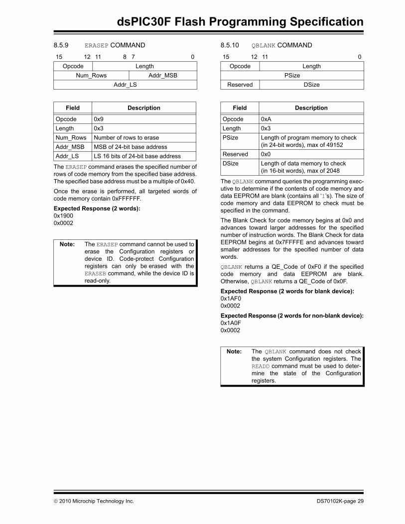
8.5.9 ERASEP COMMAND
15 12 11 8 7 0Opcode Length
Num_Rows Addr_MSBAddr_LS
Field Description
Opcode 0x9Length 0x3Num_Rows Number of rows to eraseAddr_MSB MSB of 24-bit base addressAddr_LS LS 16 bits of 24-bit base address
The ERASEP command erases the specified number of rows of code memory from the specified base address. The specified base address must be a multiple of 0x40.
Once the erase is performed, all targeted words of code memory contain 0xFFFFFF.
Expected Response (2 words): 0x1900 0x0002
Note: The ERASEP command cannot be used to erase the Configuration registers or device ID. Code-protect Configuration registers can only be erased with the ERASEB command, while the device ID is read-only.
8.5.10 QBLANK COMMAND
15 12 11 0Opcode Length
PSizeReserved DSize
Field Description
Opcode 0xALength 0x3PSize Length of program memory to check
(in 24-bit words), max of 49152Reserved 0x0DSize Length of data memory to check
(in 16-bit words), max of 2048
The QBLANK command queries the programming exec-utive to determine if the contents of code memory and data EEPROM are blank (contains all ‘1’s). The size of code memory and data EEPROM to check must be specified in the command.
The Blank Check for code memory begins at 0x0 and advances toward larger addresses for the specified number of instruction words. The Blank Check for data EEPROM begins at 0x7FFFFE and advances toward smaller addresses for the specified number of data words.
QBLANK returns a QE_Code of 0xF0 if the specified code memory and data EEPROM are blank. Otherwise, QBLANK returns a QE_Code of 0x0F.
Expected Response (2 words for blank device): 0x1AF0 0x0002
Expected Response (2 words for non-blank device): 0x1A0F 0x0002
Note: The QBLANK command does not check the system Configuration registers. The READD command must be used to deter-mine the state of the Configuration registers.
© 2010 Microchip Technology Inc. DS70102K-page 29
dsPIC30F Flash Programming Specification
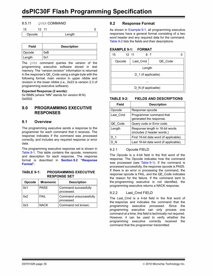
8.5.11 QVER COMMAND
15 12 11 0Opcode Length
Field Description
Opcode 0xBLength 0x1
The QVER command queries the version of the programming executive software stored in test memory. The “version.revision” information is returned in the response’s QE_Code using a single byte with the following format: main version in upper nibble and revision in the lower nibble (i.e., 0x23 is version 2.3 of programming executive software).
Expected Response (2 words): 0x1BMN (where “MN” stands for version M.N) 0x0002
9.0 PROGRAMMING EXECUTIVE RESPONSES
9.1 OverviewThe programming executive sends a response to the programmer for each command that it receives. The response indicates if the command was processed correctly, and includes any required response or error data.
The programming executive response set is shown in Table 9-1. This table contains the opcode, mnemonic and description for each response. The response format is described in Section 9.2 “Response Format”.
TABLE 9-1: PROGRAMMING EXECUTIVE RESPONSE SET
Opcode Mnemonic Description
0x1 PASS Command successfully processed.
0x2 FAIL Command unsuccessfully processed.
0x3 NACK Command not known.
9.2 Response FormatAs shown in Example 9-1, all programming executive responses have a general format consisting of a two word header and any required data for the command. Table 9-2 lists the fields and their descriptions.
EXAMPLE 9-1: FORMAT
TABLE 9-2:Field Description
Opcode Response opcode.Last_Cmd Programmer command that
generated the response.QE_Code Query code or Error code.Length Response length in 16-bit words
(includes 2 header words.)D_1 First 16-bit data word (if applicable).D_N Last 16-bit data word (if applicable).
FIELDS AND DESCRIPTIONS
9.2.1 Opcode FIELDThe Opcode is a 4-bit field in the first word of the response. The Opcode indicates how the command was processed (see Table 9-1). If the command is processed successfully, the response opcode is PASS. If there is an error in processing the command, the response opcode is FAIL, and the QE_Code indicates the reason for the failure. If the command sent to the programming executive is not identified, the programming executive returns a NACK response.
9.2.2 Last_Cmd FIELDThe Last_Cmd is a 4-bit field in the first word ofthe response and indicates the command that the programming executive processed. Since the programming executive can only process one command at a time, this field is technically not required. However, it can be used to verify whether the programming executive correctly received the command that the programmer transmitted.
15 12 11 8 7 0
Opcode Last_Cmd QE_Code
Length
D_1 (if applicable)
...
D_N (if applicable)
DS70102K-page 30 © 2010 Microchip Technology Inc.
dsPIC30F Flash Programming Specification
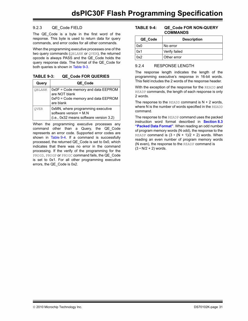
9.2.3 QE_Code FIELDThe QE_Code is a byte in the first word of the response. This byte is used to return data for query commands, and error codes for all other commands.
When the programming executive processes one of the two query commands (QBLANK or QVER), the returned opcode is always PASS and the QE_Code holds the query response data. The format of the QE_Code for both queries is shown in Table 9-3.
TABLE 9-3: QE_Code FOR QUERIES Query QE_Code
QBLANK 0x0F = Code memory and data EEPROM are NOT blank0xF0 = Code memory and data EEPROM are blank
QVER 0xMN, where programming executive software version = M.N(i.e., 0x32 means software version 3.2)
When the programming executive processes any command other than a Query, the QE_Code represents an error code. Supported error codes are shown in Table 9-4. If a command is successfully processed, the returned QE_Code is set to 0x0, which indicates that there was no error in the command processing. If the verify of the programming for the PROGD, PROGP or PROGC command fails, the QE_Code is set to 0x1. For all other programming executive errors, the QE_Code is 0x2.
TABLE 9-4: QE_Code FOR NON-QUERY COMMANDS
QE_Code Description
0x0 No error 0x1 Verify failed0x2 Other error
9.2.4 RESPONSE LENGTHThe response length indicates the length of the programming executive’s response in 16-bit words. This field includes the 2 words of the response header.
With the exception of the response for the READD and READP commands, the length of each response is only 2 words.
The response to the READD command is N + 2 words, where N is the number of words specified in the READDcommand.
The response to the READP command uses the packed instruction word format described in Section 8.3 “Packed Data Format”. When reading an odd number of program memory words (N odd), the response to the READP command is (3 • (N + 1)/2 + 2) words. When reading an even number of program memory words (N even), the response to the READP command is (3 • N/2 + 2) words.
© 2010 Microchip Technology Inc. DS70102K-page 31
dsPIC30F Flash Programming Specification
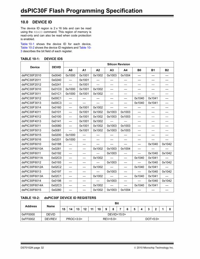
10.0 DEVICE IDThe device ID region is 2 x 16 bits and can be read using the READD command. This region of memory is read-only and can also be read when code protection is enabled.
Table 10-1 shows the device ID for each device, Table 10-2 shows the device ID registers and Table 10-3 describes the bit field of each register.
TABLE 10-1: DEVICE IDS
Device DEVIDSilicon Revision
A0 A1 A2 A3 A4 B0 B1 B2
dsPIC30F2010 0x0040 0x1000 0x1001 0x1002 0x1003 0x1004 — — —dsPIC30F2011 0x0240 — 0x1001 — — — — — —dsPIC30F2012 0x0241 — 0x1001 — — — — — —dsPIC30F3010 0x01C0 0x1000 0x1001 0x1002 — — — — —dsPIC30F3011 0x01C1 0x1000 0x1001 0x1002 — — — — —dsPIC30F3012 0x00C1 — — — — — 0x1040 0x1041 —dsPIC30F3013 0x00C3 — — — — — 0x1040 0x1041 —dsPIC30F3014 0x0160 — 0x1001 0x1002 — — — — —dsPIC30F4011 0x0101 — 0x1001 0x1002 0x1003 0x1003 — — —dsPIC30F4012 0x0100 — 0x1001 0x1002 0x1003 0x1003 — — —dsPIC30F4013 0x0141 — 0x1001 0x1002 — — — — —dsPIC30F5011 0x0080 — 0x1001 0x1002 0x1003 0x1003 — — —dsPIC30F5013 0x0081 — 0x1001 0x1002 0x1003 0x1003 — — —dsPIC30F5015 0x0200 0x1000 — — — — — — —dsPIC30F5016 0x0201 0x1000 — — — — — — —dsPIC30F6010 0x0188 — — — — — — 0x1040 0x1042dsPIC30F6010A 0x0281 — — 0x1002 0x1003 0x1004 — — —dsPIC30F6011 0x0192 — — — 0x1003 — — 0x1040 0x1042dsPIC30F6011A 0x02C0 — — 0x1002 — — 0x1040 0x1041 —dsPIC30F6012 0x0193 — — — 0x1003 — — 0x1040 0x1042dsPIC30F6012A 0x02C2 — — 0x1002 — — 0x1040 0x1041 —dsPIC30F6013 0x0197 — — — 0x1003 — — 0x1040 0x1042dsPIC30F6013A 0x02C1 — — 0x1002 — — 0x1040 0x1041 —dsPIC30F6014 0x0198 — — — 0x1003 — — 0x1040 0x1042dsPIC30F6014A 0x02C3 — — 0x1002 — — 0x1040 0x1041 —dsPIC30F6015 0x0280 — — 0x1002 0x1003 0x1004 — — —
TABLE 10-2: dsPIC30F DEVICE ID REGISTERS
Address NameBit
15 14 13 12 11 10 9 8 7 6 5 4 3 2 1 0
0xFF0000 DEVID DEVID<15:0>0xFF0002 DEVREV PROC<3:0> REV<5:0> DOT<5:0>
DS70102K-page 32 © 2010 Microchip Technology Inc.
dsPIC30F Flash Programming Specification
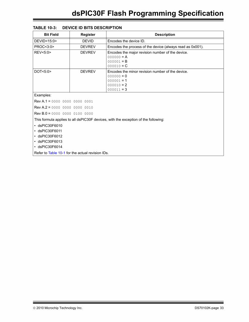
TABLE 10-3: DEVICE ID BITS DESCRIPTIONBit Field Register Description
DEVID<15:0> DEVID Encodes the device ID.PROC<3:0> DEVREV Encodes the process of the device (always read as 0x001).REV<5:0> DEVREV Encodes the major revision number of the device.
000000 = A000001 = B000010 = C
DOT<5:0> DEVREV Encodes the minor revision number of the device.000000 = 0000001 = 1000010 = 2000011 = 3
Examples:
Rev A.1 = 0000 0000 0000 0001
Rev A.2 = 0000 0000 0000 0010
Rev B.0 = 0000 0000 0100 0000
This formula applies to all dsPIC30F devices, with the exception of the following:
Refer to Table 10-1 for the actual revision IDs.
• dsPIC30F6010• dsPIC30F6011• dsPIC30F6012• dsPIC30F6013• dsPIC30F6014
© 2010 Microchip Technology Inc. DS70102K-page 33
dsPIC30F Flash Programming Specification
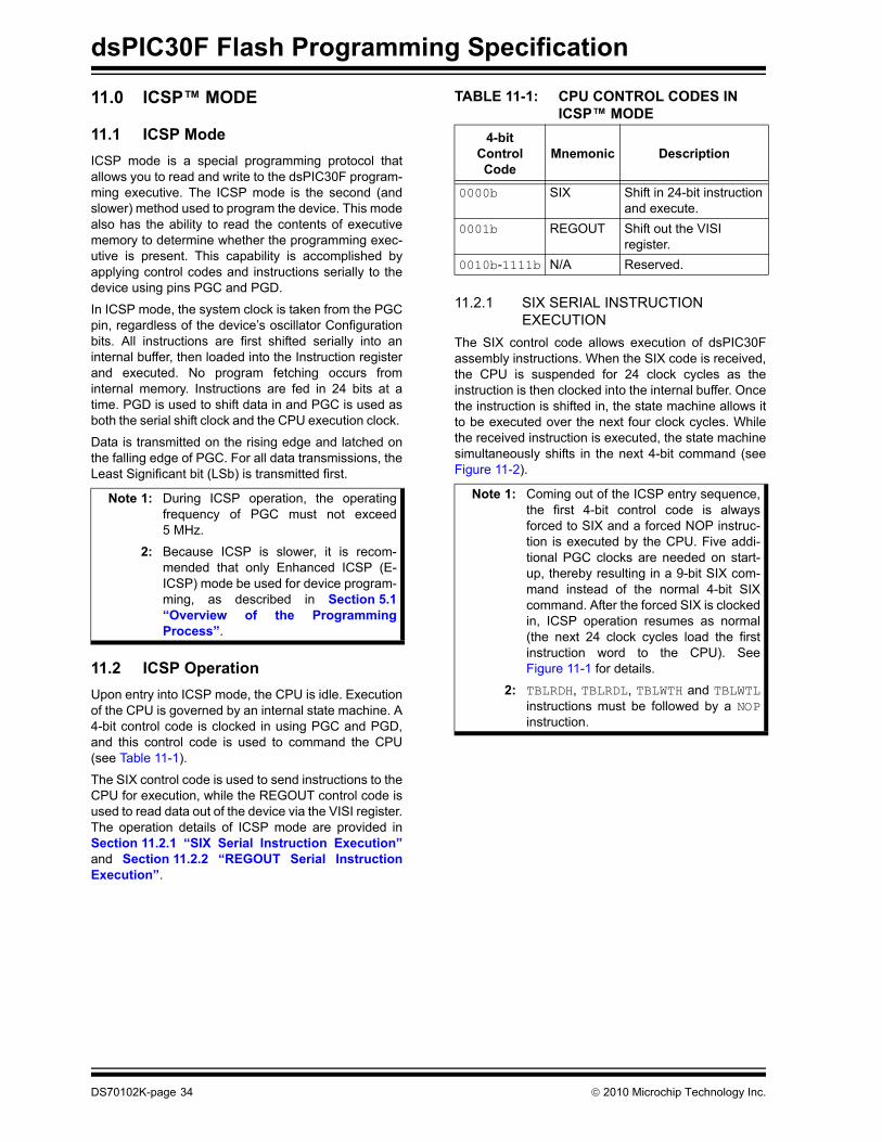
11.0 ICSP™ MODE
11.1 ICSP ModeICSP mode is a special programming protocol that allows you to read and write to the dsPIC30F program-ming executive. The ICSP mode is the second (and slower) method used to program the device. This mode also has the ability to read the contents of executive memory to determine whether the programming exec-utive is present. This capability is accomplished by applying control codes and instructions serially to the device using pins PGC and PGD.
In ICSP mode, the system clock is taken from the PGC pin, regardless of the device’s oscillator Configuration bits. All instructions are first shifted serially into an internal buffer, then loaded into the Instruction register and executed. No program fetching occurs from internal memory. Instructions are fed in 24 bits at a time. PGD is used to shift data in and PGC is used as both the serial shift clock and the CPU execution clock.
Data is transmitted on the rising edge and latched on the falling edge of PGC. For all data transmissions, the Least Significant bit (LSb) is transmitted first.
11.2 ICSP OperationUpon entry into ICSP mode, the CPU is idle. Execution of the CPU is governed by an internal state machine. A 4-bit control code is clocked in using PGC and PGD, and this control code is used to command the CPU (see Table 11-1).
The SIX control code is used to send instructions to the CPU for execution, while the REGOUT control code is used to read data out of the device via the VISI register. The operation details of ICSP mode are provided in Section 11.2.1 “SIX Serial Instruction Execution”and Section 11.2.2 “REGOUT Serial Instruction Execution”.
TABLE 11-1: CPU CONTROL CODES IN ICSP™ MODE
4-bitControlCode
Mnemonic Description
0000b SIX Shift in 24-bit instruction and execute.
0001b REGOUT Shift out the VISI register.
0010b-1111b N/A Reserved.
11.2.1 SIX SERIAL INSTRUCTION EXECUTION
The SIX control code allows execution of dsPIC30Fassembly instructions. When the SIX code is received, the CPU is suspended for 24 clock cycles as the instruction is then clocked into the internal buffer. Once the instruction is shifted in, the state machine allows it to be executed over the next four clock cycles. While the received instruction is executed, the state machine simultaneously shifts in the next 4-bit command (see Figure 11-2).
Note 1: During ICSP operation, the operating frequency of PGC must not exceed 5 MHz.
2: Because ICSP is slower, it is recom-mended that only Enhanced ICSP (E-ICSP) mode be used for device program-ming, as described in Section 5.1 “Overview of the Programming Process”.
Note 1: Coming out of the ICSP entry sequence, the first 4-bit control code is always forced to SIX and a forced NOP instruc-tion is executed by the CPU. Five addi-tional PGC clocks are needed on start-up, thereby resulting in a 9-bit SIX com-mand instead of the normal 4-bit SIX command. After the forced SIX is clocked in, ICSP operation resumes as normal (the next 24 clock cycles load the first instruction word to the CPU). See Figure 11-1 for details.
2: TBLRDH, TBLRDL, TBLWTH and TBLWTLinstructions must be followed by a NOPinstruction.
DS70102K-page 34 © 2010 Microchip Technology Inc.
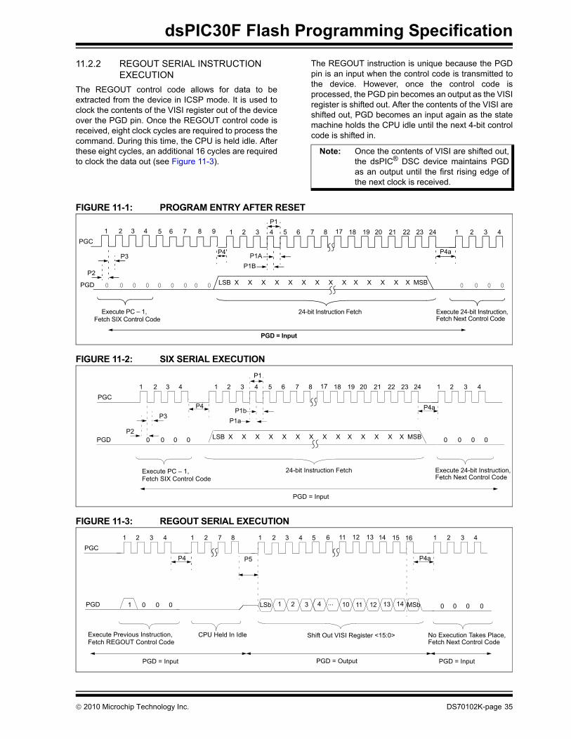
dsPIC30F Flash Programming Specification
11.2.2 REGOUT SERIAL INSTRUCTION EXECUTION
The REGOUT control code allows for data to be extracted from the device in ICSP mode. It is used to clock the contents of the VISI register out of the device over the PGD pin. Once the REGOUT control code is received, eight clock cycles are required to process the command. During this time, the CPU is held idle. After these eight cycles, an additional 16 cycles are required to clock the data out (see Figure 11-3).
The REGOUT instruction is unique because the PGD pin is an input when the control code is transmitted to the device. However, once the control code is processed, the PGD pin becomes an output as the VISI register is shifted out. After the contents of the VISI are shifted out, PGD becomes an input again as the state machine holds the CPU idle until the next 4-bit control code is shifted in.
Note: Once the contents of VISI are shifted out, the dsPIC® DSC device maintains PGD as an output until the first rising edge of the next clock is received.
FIGURE 11-1: PROGRAM ENTRY AFTER RESET
FIGURE 11-2: SIX SERIAL EXECUTION
FIGURE 11-3: REGOUT SERIAL EXECUTION
P4
2 3 1 2 3 23 24 1 2 3 4P1
PGCP4a
PGD
24-bit Instruction Fetch Execute 24-bit Instruction,Execute PC – 1,
1 4
0 0 0 0
Fetch SIX Control Code Fetch Next Control Code
4 5 6 7 8 18 19 20 21 2217
LSB X X X X X X X X X X X X X X MSB
PGD = Input
P2
P3P1B
P1A
5 6 7
0 0 0 00 0 0
8 9
0 0
P4
2 3 1 2 3 23 24 1 2 3 4
P1
PGCP4a
PGD
24-bit Instruction Fetch Execute 24-bit Instruction,Execute PC – 1,
1 4
0 0 0 0 0 0 0 0
Fetch SIX Control Code Fetch Next Control Code
4 5 6 7 8 18 19 20 21 2217
LSB X X X X X X X X X X X X X X MSB
PGD = Input
P2
P3P1a
P1b
1 2 3 4 1 2 7 8PGC
P4
PGD
PGD = Input
Execute Previous Instruction, CPU Held In Idle Shift Out VISI Register <15:0>
P5
PGD = Output
1 2 3 1 2 3 4
P4a
11 13 15 161412
No Execution Takes Place,Fetch Next Control Code
0 0 0 0 0
PGD = Input
MSb1 2 3 41
4 5 6
LSb 141312... 11100
Fetch REGOUT Control Code
0
© 2010 Microchip Technology Inc. DS70102K-page 35
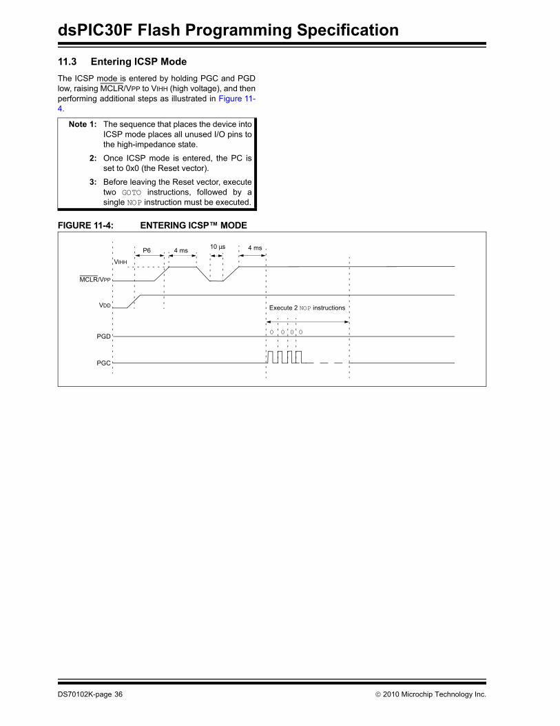
dsPIC30F Flash Programming Specification
11.3 Entering ICSP ModeThe ICSP mode is entered by holding PGC and PGD low, raising MCLR/VPP to VIHH (high voltage), and then performing additional steps as illustrated in Figure 11-4.
FIGURE 11-4: ENTERING ICSP™ MODE
Note 1: The sequence that places the device into ICSP mode places all unused I/O pins to the high-impedance state.
2: Once ICSP mode is entered, the PC is set to 0x0 (the Reset vector).
3: Before leaving the Reset vector, execute two GOTO instructions, followed by a single NOP instruction must be executed.
MCLR/VPP
VDD
PGD
PGC
Execute 2 NOP instructions
0 0 0 0
4 msP6 4 ms
VIHH
10 μs
DS70102K-page 36 © 2010 Microchip Technology Inc.
dsPIC30F Flash Programming Specification
11.4 Flash Memory Programming in ICSP Mode
Programming in ICSP mode is described in Section 11.4.1 “Programming Operations” through Section 11.4.3 “Starting and Stopping a Program-ming Cycle”. Step-by-step procedures are described in Section 11.5 “Erasing Program Memory in Normal-Voltage Systems” through Section 11.13 “Reading the Application ID Word”. All programming operations must use serial execution, as described in Section 11.2 “ICSP Operation”.
11.4.1 PROGRAMMING OPERATIONS Flash memory write and erase operations are controlled by the NVMCON register. Programming is performed by setting NVMCON to select the type of erase operation (Table 11-2) or write operation (Table 11-3), writing a key sequence to enable the programming and initiating the programming by setting the WR control bit, NVMCON<15>.
In ICSP mode, all programming operations are externally timed. An external 2 ms delay must be used between setting the WR control bit and clearing the WR control bit to complete the programming operation.
TABLE 11-2: NVMCON ERASE OPERATIONS
NVMCONValue Erase Operation
0x407F Erase all code memory, data memory (does not erase UNIT ID).
0x4075 Erase 1 row (16 words) of dataEEPROM.
0x4074 Erase 1 word of data EEPROM.0x4072 Erase all executive memory.0x4071 Erase 1 row (32 instruction words)
from 1 panel of code memory.0x406E Erase Boot Secure and General
Segments, then erase FBS, FSS and FGS configuration registers.
0x4066 Erase all Data EEPROM allocated to Boot Segment.
0x405E Erase Secure and General Segments, then erase FSS and FGS configuration registers.
0x4056 Erase all Data EEPROM allocated to Secure Segment.
0x404E Erase General Segment, then erase FGS configuration register.
0x4046 Erase all Data EEPROM allocated to General Segment.
TABLE 11-3: NVMCON WRITE OPERATIONS
NVMCONValue Write Operation
0x4008 Write 1 word to configurationmemory.
0x4005 Write 1 row (16 words) to data memory.0x4004 Write 1 word to data memory.0x4001 Write 1 row (32 instruction words) into
1 panel of program memory.
11.4.2 UNLOCKING NVMCON FOR PROGRAMMING
Writes to the WR bit (NVMCON<15>) are locked to prevent accidental programming from taking place. Writing a key sequence to the NVMKEY register unlocks the WR bit and allows it to be written to. The unlock sequence is performed as follows:
MOV #0x55, W8MOV W8, NVMKEYMOV #0xAA, W9MOV W9, NVMKEY
Note: Any working register, or working register pair, can be used to write the unlock sequence.
11.4.3 STARTING AND STOPPING A PROGRAMMING CYCLE
Once the unlock key sequence has been written to the NVMKEY register, the WR bit (NVMCON<15>) is used to start and stop an erase or write cycle. Setting the WR bit initiates the programming cycle. Clearing the WR bit terminates the programming cycle.
All erase and write cycles must be externally timed. An external delay must be used between setting and clearing the WR bit. Starting and stopping a programming cycle is performed as follows:
BSET NVMCON, #WR<Wait 2 ms>BCLR NVMCON, #WR
11.5 Erasing Program Memory in Normal-Voltage Systems
The procedure for erasing program memory (all code memory, data memory, executive memory and code-protect bits) consists of setting NVMCON to 0x407F, unlocking NVMCON for erasing and then executing the programming cycle. This method of bulk erasing pro-gram memory only works for systems where VDD is between 4.5 volts and 5.5 volts. The method for erasing program memory for systems with a lower VDD (3.0 volts-4.5 volts) is described in Section 6.1 “Erasing Memory”.
© 2010 Microchip Technology Inc. DS70102K-page 37
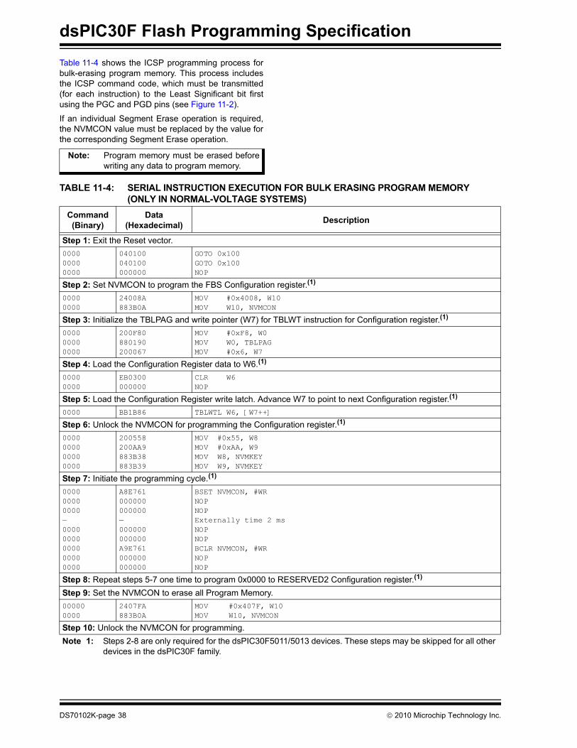
dsPIC30F Flash Programming Specification
Table 11-4 shows the ICSP programming process for bulk-erasing program memory. This process includes the ICSP command code, which must be transmitted (for each instruction) to the Least Significant bit first using the PGC and PGD pins (see Figure 11-2).If an individual Segment Erase operation is required, the NVMCON value must be replaced by the value for
Note: Program memory must be erased before writing any data to program memory.
the corresponding Segment Erase operation.
TABLE 11-4: SERIAL INSTRUCTION EXECUTION FOR BULK ERASING PROGRAM MEMORY (ONLY IN NORMAL-VOLTAGE SYSTEMS)
Command(Binary)
Data(Hexadecimal) Description
Step 1: Exit the Reset vector.000000000000
040100040100000000
GOTO 0x100GOTO 0x100NOP
Step 2: Set NVMCON to program the FBS Configuration register.(1)
00000000
24008A883B0A
MOV #0x4008, W10MOV W10, NVMCON
Step 3: Initialize the TBLPAG and write pointer (W7) for TBLWT instruction for Configuration register.(1)
000000000000
200F80880190200067
MOV #0xF8, W0MOV W0, TBLPAGMOV #0x6, W7
Step 4: Load the Configuration Register data to W6.(1)
00000000
EB0300000000
CLR W6NOP
Step 5: Load the Configuration Register write latch. Advance W7 to point to next Configuration register.(1)
0000 BB1B86 TBLWTL W6, [W7++]
Step 6: Unlock the NVMCON for programming the Configuration register.(1)
0000000000000000
200558 200AA9 883B38 883B39
MOV #0x55, W8 MOV #0xAA, W9 MOV W8, NVMKEY MOV W9, NVMKEY
Step 7: Initiate the programming cycle.(1)
000000000000—00000000000000000000
A8E761000000000000 —000000000000A9E761000000000000
BSET NVMCON, #WR NOPNOPExternally time 2 msNOPNOPBCLR NVMCON, #WRNOPNOP
Step 8: Repeat steps 5-7 one time to program 0x0000 to RESERVED2 Configuration register.(1)
Step 9: Set the NVMCON to erase all Program Memory.000000000
2407FA 883B0A
MOV #0x407F, W10 MOV W10, NVMCON
Step 10: Unlock the NVMCON for programming.Note 1: Steps 2-8 are only required for the dsPIC30F5011/5013 devices. These steps may be skipped for all other
devices in the dsPIC30F family.
DS70102K-page 38 © 2010 Microchip Technology Inc.
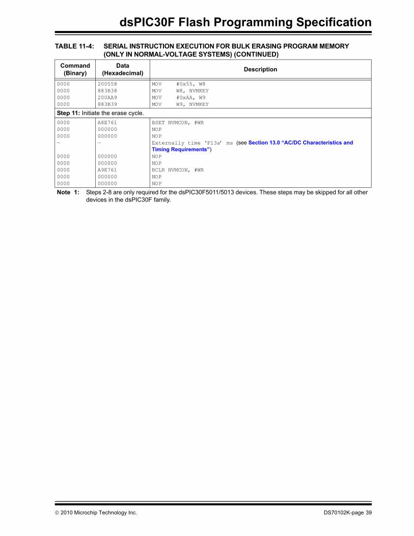
dsPIC30F Flash Programming Specification
0000000000000000
200558 883B38 200AA9 883B39
MOV #0x55, W8 MOV W8, NVMKEY MOV #0xAA, W9 MOV W9, NVMKEY
Step 11: Initiate the erase cycle.000000000000—
00000000000000000000
A8E761000000000000 —
000000000000A9E761000000000000
BSET NVMCON, #WR NOPNOPExternally time ‘P13a’ ms (see Section 13.0 “AC/DC Characteristics and Timing Requirements”)NOPNOPBCLR NVMCON, #WRNOPNOP
TABLE 11-4: SERIAL INSTRUCTION EXECUTION FOR BULK ERASING PROGRAM MEMORY (ONLY IN NORMAL-VOLTAGE SYSTEMS) (CONTINUED)
Command(Binary)
Data(Hexadecimal) Description
Note 1: Steps 2-8 are only required for the dsPIC30F5011/5013 devices. These steps may be skipped for all other devices in the dsPIC30F family.
© 2010 Microchip Technology Inc. DS70102K-page 39

dsPIC30F Flash Programming Specification
11.6 Erasing Program Memory in Low-Voltage Systems
The procedure for erasing program memory (all code memory and data memory) in low-voltage systems (with VDD between 2.5 volts and 4.5 volts) is quite different than the procedure for erasing program memory in normal-voltage systems. Instead of using a Bulk Erase operation, each region of memory must be individually erased by row. Namely, all of the code memory, executive memory and data memory must be erased one row at a time. This procedure is detailed in Table 11-5.
Due to security restrictions, the FBS, FSS and FGS register cannot be erased in low-voltage systems. Once any bits in the FGS register are programmed to ‘0’, they can only be set back to ‘1’ by performing a Bulk Erase in a normal-voltage system. Alternatively, a Seg-ment Erase operation can be performed instead of a Bulk Erase.
Normal-voltage systems can also be used to erase program memory as shown in Table 11-5. However, since this method is more time-consuming and does not clear the code-protect bits, it is not recommended.
Note: Program memory must be erased before writing any data to program memory.
TABLE 11-5: SERIAL INSTRUCTION EXECUTION FOR ERASING PROGRAM MEMORY (EITHER IN LOW-VOLTAGE OR NORMAL-VOLTAGE SYSTEMS)
Command(Binary)
Data(Hexadecimal) Description
Step 1: Exit the Reset vector.000000000000
040100040100000000
GOTO 0x100GOTO 0x100NOP
Step 2: Initialize NVMADR and NVMADRU to erase code memory and initialize W7 for row address updates.0000000000000000
EB0300883B16883B26200407
CLR W6MOV W6, NVMADRMOV W6, NVMADRUMOV #0x40, W7
Step 3: Set NVMCON to erase 1 row of code memory. 00000000
24071A883B0A
MOV #0x4071, W10MOV W10, NVMCON
Step 4: Unlock the NVMCON to erase 1 row of code memory. 0000000000000000
200558 883B38 200AA9 883B39
MOV #0x55, W8 MOV W8, NVMKEY MOV #0xAA, W9 MOV W9, NVMKEY
Step 5: Initiate the erase cycle.000000000000—
00000000000000000000
A8E761000000000000 —
000000000000A9E761000000000000
BSET NVMCON, #WR NOPNOPExternally time ‘P13a’ ms (see Section 13.0 “AC/DC Characteristics and Timing Requirements”)NOPNOPBCLR NVMCON, #WRNOPNOP
DS70102K-page 40 © 2010 Microchip Technology Inc.
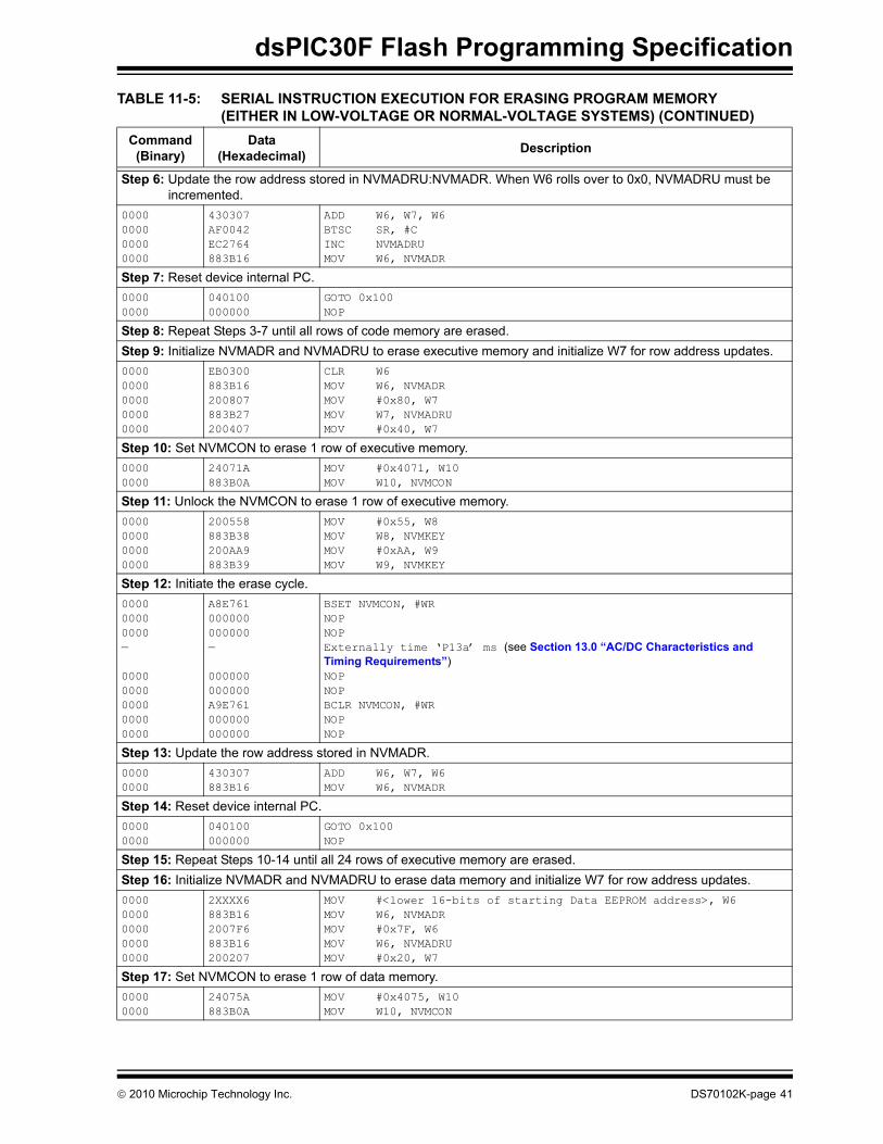
dsPIC30F Flash Programming Specification
Step 6: Update the row address stored in NVMADRU:NVMADR. When W6 rolls over to 0x0, NVMADRU must be incremented.
0000000000000000
430307AF0042EC2764883B16
ADD W6, W7, W6 BTSC SR, #CINC NVMADRUMOV W6, NVMADR
Step 7: Reset device internal PC.00000000
040100000000
GOTO 0x100NOP
Step 8: Repeat Steps 3-7 until all rows of code memory are erased.Step 9: Initialize NVMADR and NVMADRU to erase executive memory and initialize W7 for row address updates.00000000000000000000
EB0300883B16200807883B27200407
CLR W6MOV W6, NVMADRMOV #0x80, W7MOV W7, NVMADRUMOV #0x40, W7
Step 10: Set NVMCON to erase 1 row of executive memory. 00000000
24071A883B0A
MOV #0x4071, W10MOV W10, NVMCON
Step 11: Unlock the NVMCON to erase 1 row of executive memory.0000000000000000
200558 883B38 200AA9 883B39
MOV #0x55, W8 MOV W8, NVMKEY MOV #0xAA, W9 MOV W9, NVMKEY
Step 12: Initiate the erase cycle.000000000000—
00000000000000000000
A8E761000000000000 —
000000000000A9E761000000000000
BSET NVMCON, #WR NOPNOPExternally time ‘P13a’ ms (see Section 13.0 “AC/DC Characteristics and Timing Requirements”)NOPNOPBCLR NVMCON, #WRNOPNOP
Step 13: Update the row address stored in NVMADR. 00000000
430307883B16
ADD W6, W7, W6 MOV W6, NVMADR
Step 14: Reset device internal PC.00000000
040100000000
GOTO 0x100NOP
Step 15: Repeat Steps 10-14 until all 24 rows of executive memory are erased.Step 16: Initialize NVMADR and NVMADRU to erase data memory and initialize W7 for row address updates.00000000000000000000
2XXXX6883B162007F6883B16200207
MOV #<lower 16-bits of starting Data EEPROM address>, W6MOV W6, NVMADRMOV #0x7F, W6MOV W6, NVMADRUMOV #0x20, W7
Step 17: Set NVMCON to erase 1 row of data memory. 00000000
24075A883B0A
MOV #0x4075, W10MOV W10, NVMCON
TABLE 11-5: SERIAL INSTRUCTION EXECUTION FOR ERASING PROGRAM MEMORY (EITHER IN LOW-VOLTAGE OR NORMAL-VOLTAGE SYSTEMS) (CONTINUED)
Command(Binary)
Data(Hexadecimal) Description
© 2010 Microchip Technology Inc. DS70102K-page 41
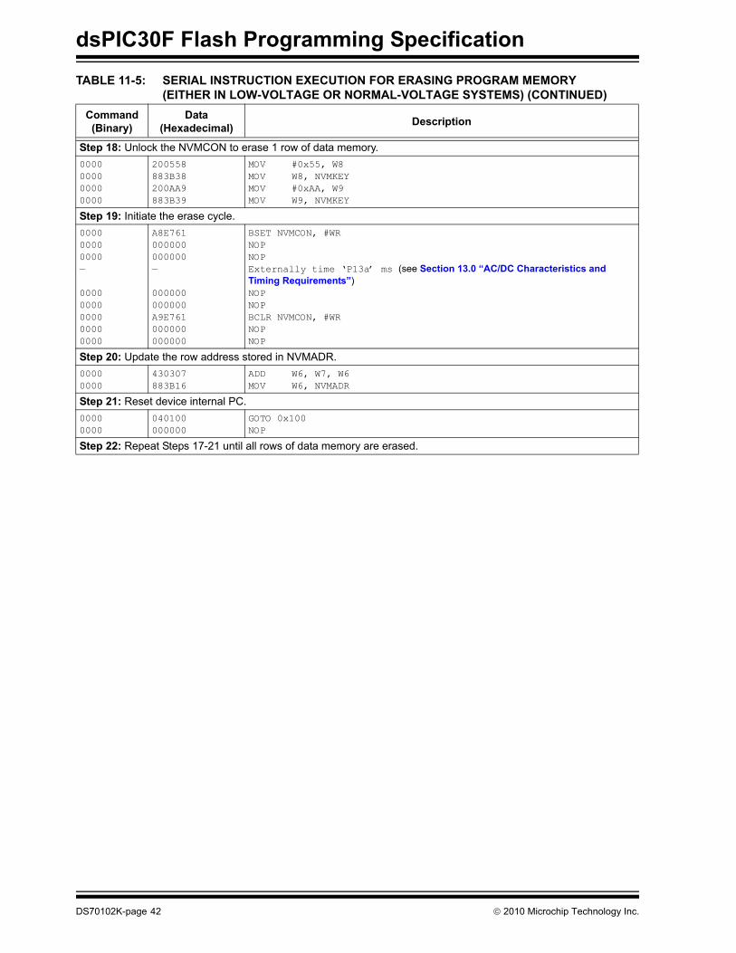
dsPIC30F Flash Programming Specification
Step 18: Unlock the NVMCON to erase 1 row of data memory.0000000000000000
200558 883B38 200AA9 883B39
MOV #0x55, W8 MOV W8, NVMKEY MOV #0xAA, W9 MOV W9, NVMKEY
Step 19: Initiate the erase cycle.000000000000—
00000000000000000000
A8E761000000000000 —
000000000000A9E761000000000000
BSET NVMCON, #WR NOPNOPExternally time ‘P13a’ ms (see Section 13.0 “AC/DC Characteristics and Timing Requirements”)NOPNOPBCLR NVMCON, #WRNOPNOP
Step 20: Update the row address stored in NVMADR. 00000000
430307883B16
ADD W6, W7, W6 MOV W6, NVMADR
Step 21: Reset device internal PC.00000000
040100000000
GOTO 0x100NOP
Step 22: Repeat Steps 17-21 until all rows of data memory are erased.
TABLE 11-5: SERIAL INSTRUCTION EXECUTION FOR ERASING PROGRAM MEMORY (EITHER IN LOW-VOLTAGE OR NORMAL-VOLTAGE SYSTEMS) (CONTINUED)
Command(Binary)
Data(Hexadecimal) Description
DS70102K-page 42 © 2010 Microchip Technology Inc.
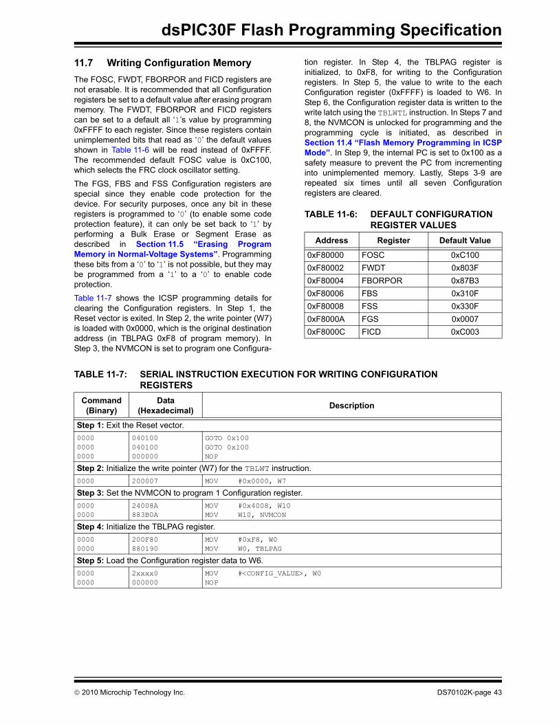
dsPIC30F Flash Programming Specification
11.7 Writing Configuration MemoryThe FOSC, FWDT, FBORPOR and FICD registers are not erasable. It is recommended that all Configuration registers be set to a default value after erasing program memory. The FWDT, FBORPOR and FICD registers can be set to a default all ‘1’s value by programming 0xFFFF to each register. Since these registers contain unimplemented bits that read as ‘0’ the default values shown in Table 11-6 will be read instead of 0xFFFF. The recommended default FOSC value is 0xC100, which selects the FRC clock oscillator setting.
The FGS, FBS and FSS Configuration registers are special since they enable code protection for the device. For security purposes, once any bit in these registers is programmed to ‘0’ (to enable some code protection feature), it can only be set back to ‘1’ by performing a Bulk Erase or Segment Erase as described in Section 11.5 “Erasing Program Memory in Normal-Voltage Systems”. Programming these bits from a ‘0’ to ‘1’ is not possible, but they may be programmed from a ‘1’ to a ‘0’ to enable code protection.
Table 11-7 shows the ICSP programming details for clearing the Configuration registers. In Step 1, the Reset vector is exited. In Step 2, the write pointer (W7) is loaded with 0x0000, which is the original destination address (in TBLPAG 0xF8 of program memory). In Step 3, the NVMCON is set to program one Configura-
tion register. In Step 4, the TBLPAG register is initialized, to 0xF8, for writing to the Configuration registers. In Step 5, the value to write to the each Configuration register (0xFFFF) is loaded to W6. In Step 6, the Configuration register data is written to the write latch using the TBLWTL instruction. In Steps 7 and 8, the NVMCON is unlocked for programming and the programming cycle is initiated, as described in Section 11.4 “Flash Memory Programming in ICSP Mode”. In Step 9, the internal PC is set to 0x100 as a safety measure to prevent the PC from incrementing into unimplemented memory. Lastly, Steps 3-9 are repeated six times until all seven Configuration registers are cleared.
TABLE 11-6: DEFAULT CONFIGURATION REGISTER VALUES
Address Register Default Value
0xF80000 FOSC 0xC1000xF80002 FWDT 0x803F0xF80004 FBORPOR 0x87B30xF80006 FBS 0x310F0xF80008 FSS 0x330F0xF8000A FGS 0x00070xF8000C FICD 0xC003
TABLE 11-7: SERIAL INSTRUCTION EXECUTION FOR WRITING CONFIGURATION REGISTERS
Command(Binary)
Data(Hexadecimal) Description
Step 1: Exit the Reset vector.000000000000
040100040100000000
GOTO 0x100GOTO 0x100NOP
Step 2: Initialize the write pointer (W7) for the TBLWT instruction.0000 200007 MOV #0x0000, W7
Step 3: Set the NVMCON to program 1 Configuration register.00000000
24008A 883B0A
MOV #0x4008, W10MOV W10, NVMCON
Step 4: Initialize the TBLPAG register.00000000
200F80 880190
MOV #0xF8, W0MOV W0, TBLPAG
Step 5: Load the Configuration register data to W6.00000000
2xxxx0000000
MOV #<CONFIG_VALUE>, W0NOP
© 2010 Microchip Technology Inc. DS70102K-page 43
dsPIC30F Flash Programming Specification
Step 6: Write the Configuration register data to the write latch and increment the write pointer.000000000000
BB1B96000000000000
TBLWTL W6, [W7++]NOPNOP
Step 7: Unlock the NVMCON for programming.0000000000000000
200558 883B38 200AA9 883B39
MOV #0x55, W8MOV W8, NVMKEYMOV #0xAA, W9MOV W9, NVMKEY
Step 8: Initiate the write cycle.000000000000—
00000000000000000000
A8E761000000000000 —
000000000000A9E761000000000000
BSET NVMCON, #WRNOPNOPExternally time ‘P12a’ ms (see Section 13.0 “AC/DC Characteristics and Timing Requirements”)NOPNOPBCLR NVMCON, #WRNOPNOP
Step 9: Reset device internal PC.00000000
040100000000
GOTO 0x100NOP
Step 10: Repeat steps 3-9 until all 7 Configuration registers are cleared.
TABLE 11-7: SERIAL INSTRUCTION EXECUTION FOR WRITING CONFIGURATION REGISTERS (CONTINUED)
Command(Binary)
Data(Hexadecimal) Description
DS70102K-page 44 © 2010 Microchip Technology Inc.
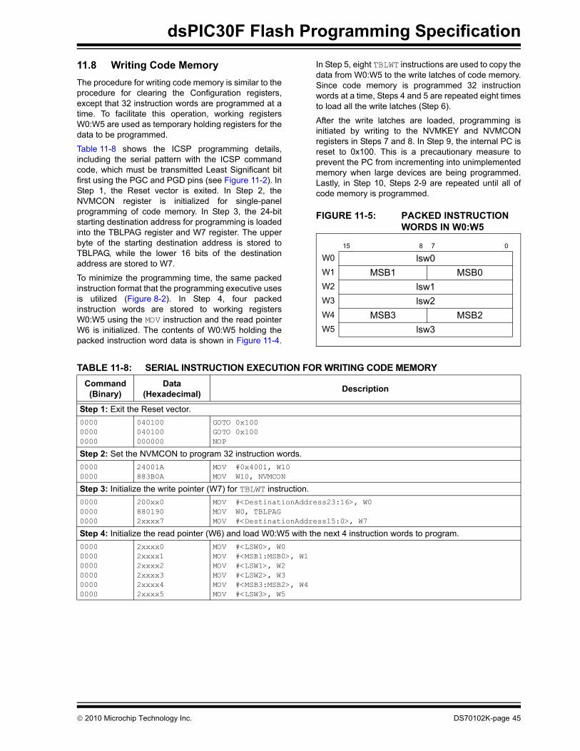
dsPIC30F Flash Programming Specification
11.8 Writing Code MemoryThe procedure for writing code memory is similar to the procedure for clearing the Configuration registers, except that 32 instruction words are programmed at a time. To facilitate this operation, working registers W0:W5 are used as temporary holding registers for the data to be programmed.
Table 11-8 shows the ICSP programming details, including the serial pattern with the ICSP command code, which must be transmitted Least Significant bit first using the PGC and PGD pins (see Figure 11-2). In Step 1, the Reset vector is exited. In Step 2, the NVMCON register is initialized for single-panel programming of code memory. In Step 3, the 24-bit starting destination address for programming is loaded into the TBLPAG register and W7 register. The upper byte of the starting destination address is stored to TBLPAG, while the lower 16 bits of the destination address are stored to W7.
To minimize the programming time, the same packed instruction format that the programming executive uses is utilized (Figure 8-2). In Step 4, four packed instruction words are stored to working registers W0:W5 using the MOV instruction and the read pointer W6 is initialized. The contents of W0:W5 holding the packed instruction word data is shown in Figure 11-4.
In Step 5, eight TBLWT instructions are used to copy the data from W0:W5 to the write latches of code memory. Since code memory is programmed 32 instruction words at a time, Steps 4 and 5 are repeated eight times to load all the write latches (Step 6).
After the write latches are loaded, programming is initiated by writing to the NVMKEY and NVMCON registers in Steps 7 and 8. In Step 9, the internal PC is reset to 0x100. This is a precautionary measure to prevent the PC from incrementing into unimplemented memory when large devices are being programmed. Lastly, in Step 10, Steps 2-9 are repeated until all of code memory is programmed.
FIGURE 11-5: PACKED INSTRUCTION WORDS IN W0:W5
15 8 7 0
W0 lsw0W1 MSB1 MSB0W2 lsw1W3 lsw2W4 MSB3 MSB2W5 lsw3
TABLE 11-8: SERIAL INSTRUCTION EXECUTION FOR WRITING CODE MEMORY Command(Binary)
Data(Hexadecimal) Description
Step 1: Exit the Reset vector.000000000000
040100040100000000
GOTO 0x100GOTO 0x100NOP
Step 2: Set the NVMCON to program 32 instruction words.00000000
24001A 883B0A
MOV #0x4001, W10MOV W10, NVMCON
Step 3: Initialize the write pointer (W7) for TBLWT instruction.000000000000
200xx0 880190 2xxxx7
MOV #<DestinationAddress23:16>, W0MOV W0, TBLPAGMOV #<DestinationAddress15:0>, W7
Step 4: Initialize the read pointer (W6) and load W0:W5 with the next 4 instruction words to program.000000000000000000000000
2xxxx0 2xxxx1 2xxxx2 2xxxx3 2xxxx4 2xxxx5
MOV #<LSW0>, W0MOV #<MSB1:MSB0>, W1MOV #<LSW1>, W2MOV #<LSW2>, W3MOV #<MSB3:MSB2>, W4MOV #<LSW3>, W5
© 2010 Microchip Technology Inc. DS70102K-page 45
dsPIC30F Flash Programming Specification
Step 5: Set the read pointer (W6) and load the (next set of) write latches.00000000000000000000000000000000000000000000000000000000000000000000000000000000000000000000000000000000
EB0300000000BB0BB6 000000000000 BBDBB6000000000000 BBEBB6 000000000000 BB1BB6000000000000BB0BB6 000000000000 BBDBB6 000000 000000 BBEBB6 000000000000 BB1BB6 000000000000
CLR W6NOPTBLWTL [W6++], [W7] NOPNOP TBLWTH.B [W6++], [W7++] NOPNOP TBLWTH.B [W6++], [++W7] NOPNOP TBLWTL [W6++], [W7++] NOP NOP TBLWTL [W6++], [W7] NOPNOP TBLWTH.B [W6++], [W7++] NOP NOP TBLWTH.B [W6++], [++W7] NOPNOPTBLWTL [W6++], [W7++] NOPNOP
Step 6: Repeat steps 4-5 eight times to load the write latches for 32 instructions.Step 7: Unlock the NVMCON for writing.0000000000000000
200558 883B38 200AA9 883B39
MOV #0x55, W8 MOV W8, NVMKEY MOV #0xAA, W9 MOV W9, NVMKEY
Step 8: Initiate the write cycle.000000000000—
00000000000000000000
A8E761000000000000—
000000000000A9E761000000000000
BSET NVMCON, #WR NOPNOPExternally time ‘P12a’ ms (see Section 13.0 “AC/DC Characteristics and Timing Requirements”)NOPNOPBCLR NVMCON, #WRNOPNOP
Step 9: Reset device internal PC.00000000
040100 000000
GOTO 0x100 NOP
Step 10: Repeat steps 2-9 until all code memory is programmed.
TABLE 11-8: SERIAL INSTRUCTION EXECUTION FOR WRITING CODE MEMORY (CONTINUED)Command(Binary)
Data(Hexadecimal) Description
DS70102K-page 46 © 2010 Microchip Technology Inc.
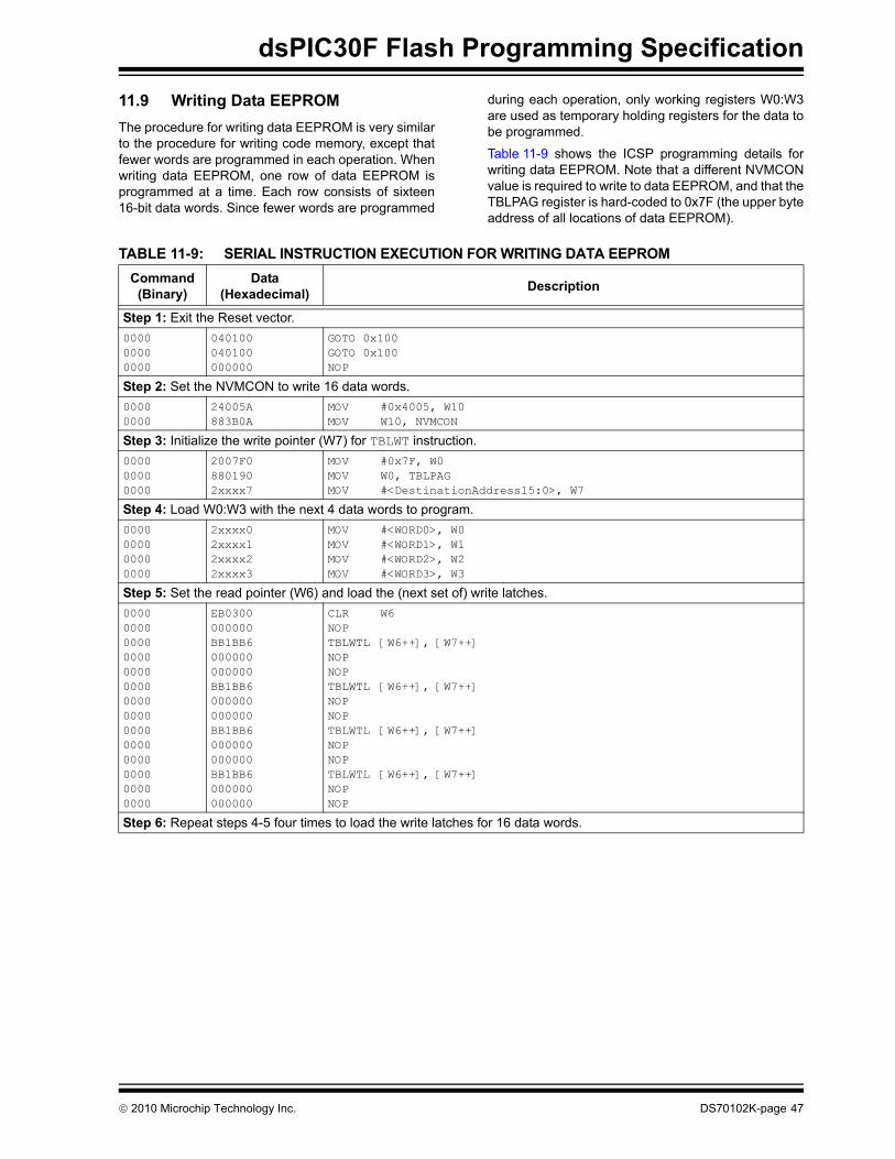
dsPIC30F Flash Programming Specification
11.9 Writing Data EEPROMThe procedure for writing data EEPROM is very similar to the procedure for writing code memory, except that fewer words are programmed in each operation. When writing data EEPROM, one row of data EEPROM is programmed at a time. Each row consists of sixteen 16-bit data words. Since fewer words are programmed
during each operation, only working registers W0:W3 are used as temporary holding registers for the data to be programmed.
Table 11-9 shows the ICSP programming details for writing data EEPROM. Note that a different NVMCON value is required to write to data EEPROM, and that the TBLPAG register is hard-coded to 0x7F (the upper byte address of all locations of data EEPROM).
TABLE 11-9: SERIAL INSTRUCTION EXECUTION FOR WRITING DATA EEPROM Command
(Binary)Data
(Hexadecimal) Description
Step 1: Exit the Reset vector.000000000000
040100040100000000
GOTO 0x100GOTO 0x100NOP
Step 2: Set the NVMCON to write 16 data words.00000000
24005A 883B0A
MOV #0x4005, W10 MOV W10, NVMCON
Step 3: Initialize the write pointer (W7) for TBLWT instruction.000000000000
2007F0 880190 2xxxx7
MOV #0x7F, W0MOV W0, TBLPAGMOV #<DestinationAddress15:0>, W7
Step 4: Load W0:W3 with the next 4 data words to program.0000000000000000
2xxxx0 2xxxx1 2xxxx2 2xxxx3
MOV #<WORD0>, W0 MOV #<WORD1>, W1 MOV #<WORD2>, W2 MOV #<WORD3>, W3
Step 5: Set the read pointer (W6) and load the (next set of) write latches.00000000000000000000000000000000000000000000000000000000
EB0300000000BB1BB6 000000000000 BB1BB6000000 000000 BB1BB6 000000000000 BB1BB6 000000 000000
CLR W6NOPTBLWTL [W6++], [W7++] NOPNOPTBLWTL [W6++], [W7++] NOP NOPTBLWTL [W6++], [W7++] NOPNOPTBLWTL [W6++], [W7++] NOPNOP
Step 6: Repeat steps 4-5 four times to load the write latches for 16 data words.
© 2010 Microchip Technology Inc. DS70102K-page 47
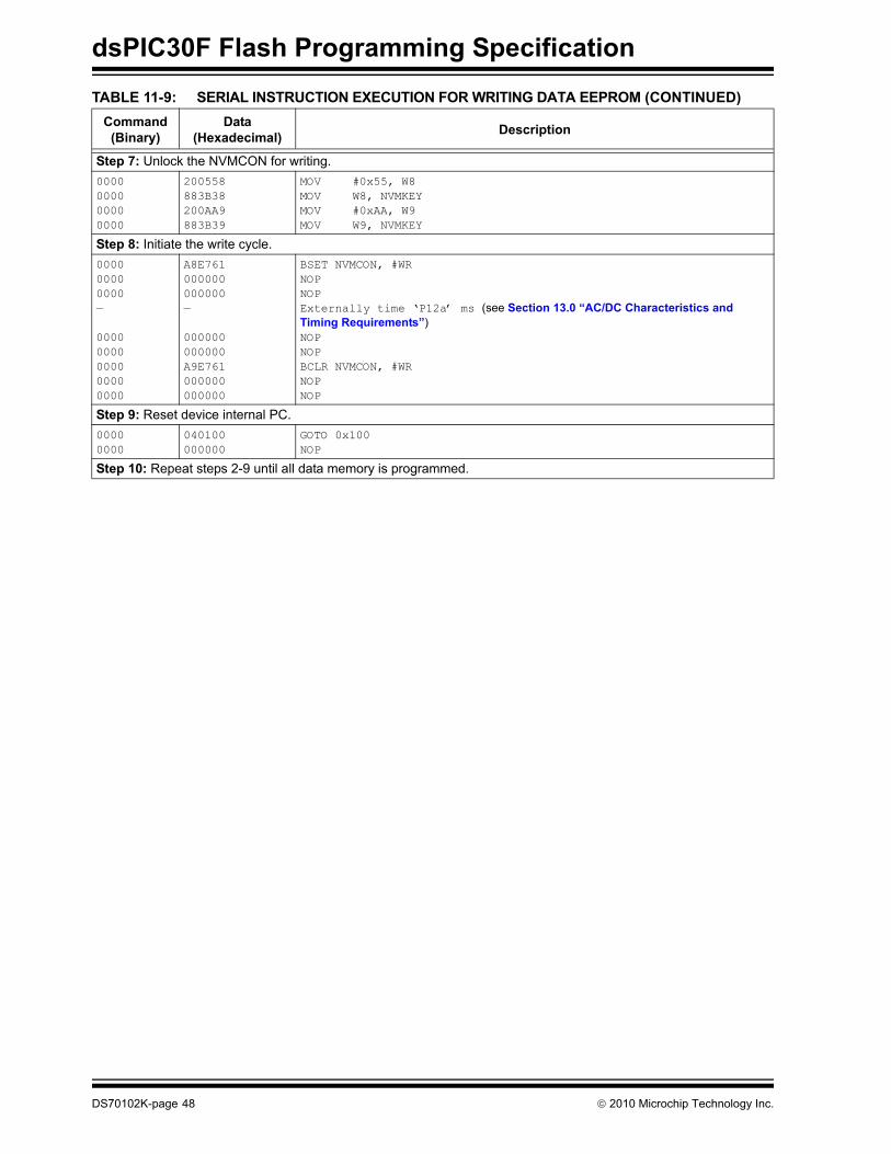
dsPIC30F Flash Programming Specification
Step 7: Unlock the NVMCON for writing.0000000000000000
200558 883B38 200AA9 883B39
MOV #0x55, W8 MOV W8, NVMKEY MOV #0xAA, W9 MOV W9, NVMKEY
Step 8: Initiate the write cycle.000000000000—
00000000000000000000
A8E761000000000000 —
000000000000A9E761000000000000
BSET NVMCON, #WR NOPNOPExternally time ‘P12a’ ms (see Section 13.0 “AC/DC Characteristics and Timing Requirements”)NOPNOPBCLR NVMCON, #WRNOPNOP
Step 9: Reset device internal PC.00000000
040100 000000
GOTO 0x100 NOP
Step 10: Repeat steps 2-9 until all data memory is programmed.
TABLE 11-9: SERIAL INSTRUCTION EXECUTION FOR WRITING DATA EEPROM (CONTINUED)Command
(Binary)Data
(Hexadecimal) Description
DS70102K-page 48 © 2010 Microchip Technology Inc.
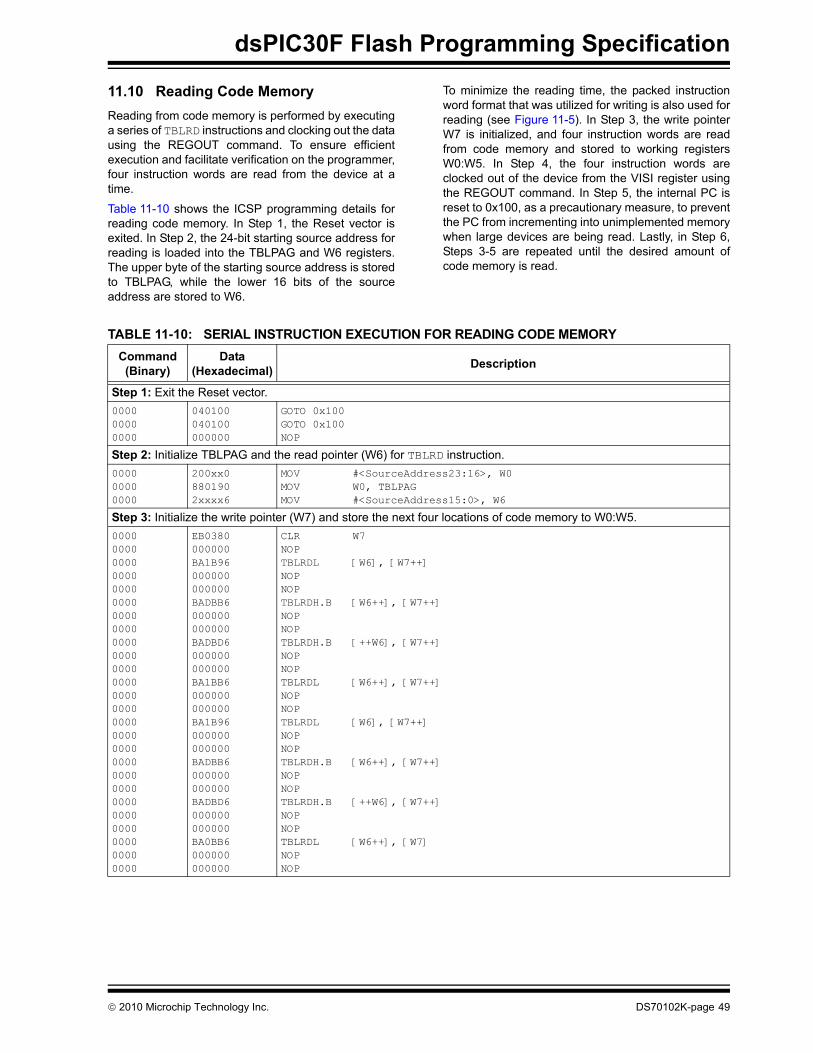
dsPIC30F Flash Programming Specification
11.10 Reading Code MemoryReading from code memory is performed by executing a series of TBLRD instructions and clocking out the data using the REGOUT command. To ensure efficient execution and facilitate verification on the programmer, four instruction words are read from the device at a time.
Table 11-10 shows the ICSP programming details for reading code memory. In Step 1, the Reset vector is exited. In Step 2, the 24-bit starting source address for reading is loaded into the TBLPAG and W6 registers. The upper byte of the starting source address is stored to TBLPAG, while the lower 16 bits of the source address are stored to W6.
To minimize the reading time, the packed instruction word format that was utilized for writing is also used for reading (see Figure 11-5). In Step 3, the write pointer W7 is initialized, and four instruction words are read from code memory and stored to working registers W0:W5. In Step 4, the four instruction words are clocked out of the device from the VISI register using the REGOUT command. In Step 5, the internal PC is reset to 0x100, as a precautionary measure, to prevent the PC from incrementing into unimplemented memory when large devices are being read. Lastly, in Step 6, Steps 3-5 are repeated until the desired amount of code memory is read.
TABLE 11-10: SERIAL INSTRUCTION EXECUTION FOR READING CODE MEMORY Command(Binary)
Data(Hexadecimal) Description
Step 1: Exit the Reset vector.000000000000
040100040100000000
GOTO 0x100GOTO 0x100NOP
Step 2: Initialize TBLPAG and the read pointer (W6) for TBLRD instruction.000000000000
200xx0 880190 2xxxx6
MOV #<SourceAddress23:16>, W0MOV W0, TBLPAGMOV #<SourceAddress15:0>, W6
Step 3: Initialize the write pointer (W7) and store the next four locations of code memory to W0:W5.00000000000000000000000000000000000000000000000000000000000000000000000000000000000000000000000000000000
EB0380000000BA1B96000000000000BADBB6000000000000BADBD6000000000000BA1BB6000000000000BA1B96000000000000BADBB6000000000000BADBD6000000000000BA0BB6000000000000
CLR W7 NOPTBLRDL [W6], [W7++] NOPNOPTBLRDH.B [W6++], [W7++] NOPNOPTBLRDH.B [++W6], [W7++] NOPNOPTBLRDL [W6++], [W7++] NOPNOPTBLRDL [W6], [W7++] NOPNOPTBLRDH.B [W6++], [W7++] NOPNOPTBLRDH.B [++W6], [W7++] NOPNOPTBLRDL [W6++], [W7] NOPNOP
© 2010 Microchip Technology Inc. DS70102K-page 49
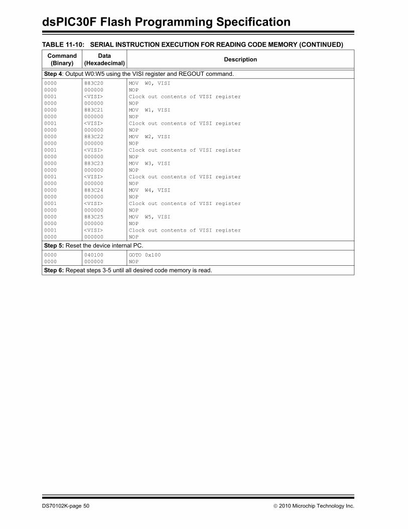
dsPIC30F Flash Programming Specification
Step 4: Output W0:W5 using the VISI register and REGOUT command.000000000001000000000000000100000000000000010000000000000001000000000000000100000000000000010000
883C20000000<VISI>000000883C21000000<VISI>000000883C22000000<VISI>000000883C23000000<VISI>000000883C24000000<VISI>000000883C25000000<VISI>000000
MOV W0, VISI NOPClock out contents of VISI registerNOPMOV W1, VISI NOPClock out contents of VISI registerNOPMOV W2, VISI NOPClock out contents of VISI registerNOPMOV W3, VISI NOPClock out contents of VISI registerNOPMOV W4, VISI NOPClock out contents of VISI registerNOPMOV W5, VISI NOPClock out contents of VISI registerNOP
Step 5: Reset the device internal PC.00000000
040100 000000
GOTO 0x100 NOP
Step 6: Repeat steps 3-5 until all desired code memory is read.
TABLE 11-10: SERIAL INSTRUCTION EXECUTION FOR READING CODE MEMORY (CONTINUED)Command(Binary)
Data(Hexadecimal) Description
DS70102K-page 50 © 2010 Microchip Technology Inc.
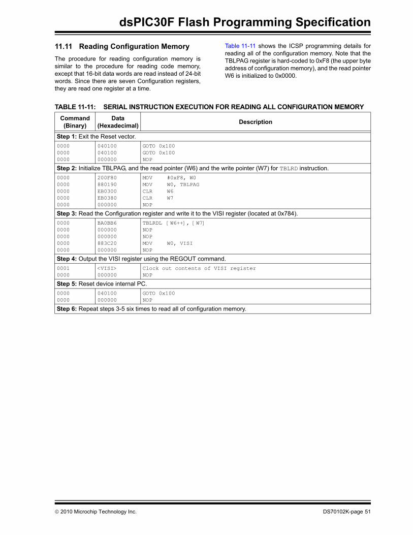
dsPIC30F Flash Programming Specification
11.11 Reading Configuration MemoryThe procedure for reading configuration memory is similar to the procedure for reading code memory, except that 16-bit data words are read instead of 24-bit words. Since there are seven Configuration registers, they are read one register at a time.
Table 11-11 shows the ICSP programming details for reading all of the configuration memory. Note that the TBLPAG register is hard-coded to 0xF8 (the upper byte address of configuration memory), and the read pointer W6 is initialized to 0x0000.
TABLE 11-11: SERIAL INSTRUCTION EXECUTION FOR READING ALL CONFIGURATION MEMORYCommand(Binary)
Data(Hexadecimal) Description
Step 1: Exit the Reset vector.000000000000
040100040100000000
GOTO 0x100GOTO 0x100NOP
Step 2: Initialize TBLPAG, and the read pointer (W6) and the write pointer (W7) for TBLRD instruction.00000000000000000000
200F80 880190 EB0300EB0380000000
MOV #0xF8, W0MOV W0, TBLPAGCLR W6CLR W7NOP
Step 3: Read the Configuration register and write it to the VISI register (located at 0x784).00000000000000000000
BA0BB6000000000000883C20000000
TBLRDL [W6++], [W7] NOPNOPMOV W0, VISI NOP
Step 4: Output the VISI register using the REGOUT command.00010000
<VISI>000000
Clock out contents of VISI registerNOP
Step 5: Reset device internal PC.00000000
040100 000000
GOTO 0x100 NOP
Step 6: Repeat steps 3-5 six times to read all of configuration memory.
© 2010 Microchip Technology Inc. DS70102K-page 51
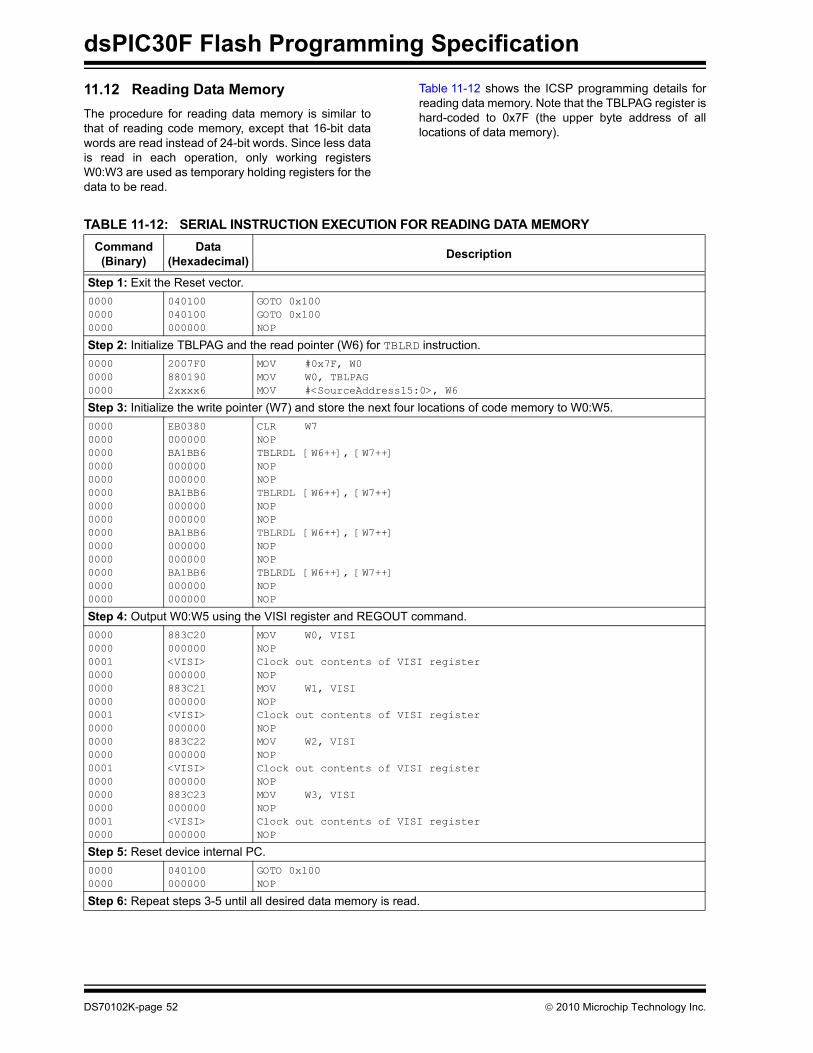
dsPIC30F Flash Programming Specification
11.12 Reading Data MemoryThe procedure for reading data memory is similar tothat of reading code memory, except that 16-bit data words are read instead of 24-bit words. Since less data is read in each operation, only working registers W0:W3 are used as temporary holding registers for the data to be read.
Table 11-12 shows the ICSP programming details for reading data memory. Note that the TBLPAG register is hard-coded to 0x7F (the upper byte address of all locations of data memory).
TABLE 11-12: SERIAL INSTRUCTION EXECUTION FOR READING DATA MEMORY Command(Binary)
Data(Hexadecimal) Description
Step 1: Exit the Reset vector.000000000000
040100040100000000
GOTO 0x100GOTO 0x100NOP
Step 2: Initialize TBLPAG and the read pointer (W6) for TBLRD instruction.000000000000
2007F0 880190 2xxxx6
MOV #0x7F, W0MOV W0, TBLPAGMOV #<SourceAddress15:0>, W6
Step 3: Initialize the write pointer (W7) and store the next four locations of code memory to W0:W5.00000000000000000000000000000000000000000000000000000000
EB0380000000BA1BB6000000000000BA1BB6000000000000BA1BB6000000000000BA1BB6000000000000
CLR W7 NOPTBLRDL [W6++], [W7++] NOPNOPTBLRDL [W6++], [W7++] NOPNOPTBLRDL [W6++], [W7++] NOPNOPTBLRDL [W6++], [W7++] NOPNOP
Step 4: Output W0:W5 using the VISI register and REGOUT command.0000000000010000000000000001000000000000000100000000000000010000
883C20000000<VISI>000000883C21000000<VISI>000000883C22000000<VISI>000000883C23000000<VISI>000000
MOV W0, VISI NOPClock out contents of VISI registerNOPMOV W1, VISI NOPClock out contents of VISI registerNOPMOV W2, VISI NOPClock out contents of VISI registerNOPMOV W3, VISI NOPClock out contents of VISI registerNOP
Step 5: Reset device internal PC.00000000
040100 000000
GOTO 0x100 NOP
Step 6: Repeat steps 3-5 until all desired data memory is read.
DS70102K-page 52 © 2010 Microchip Technology Inc.
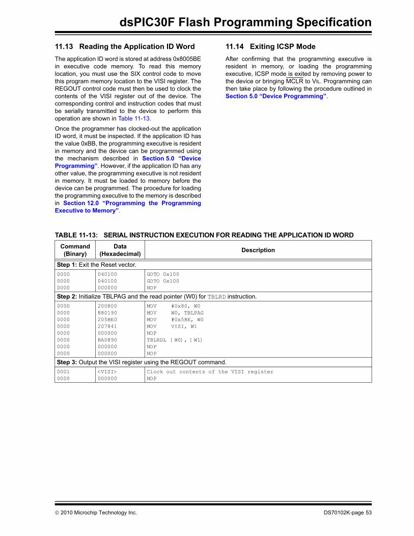
dsPIC30F Flash Programming Specification
11.13 Reading the Application ID WordThe application ID word is stored at address 0x8005BE in executive code memory. To read this memory location, you must use the SIX control code to move this program memory location to the VISI register. The REGOUT control code must then be used to clock the contents of the VISI register out of the device. The corresponding control and instruction codes that must be serially transmitted to the device to perform this operation are shown in Table 11-13.
Once the programmer has clocked-out the application ID word, it must be inspected. If the application ID has the value 0xBB, the programming executive is resident in memory and the device can be programmed using the mechanism described in Section 5.0 “Device Programming”. However, if the application ID has any other value, the programming executive is not resident in memory. It must be loaded to memory before the device can be programmed. The procedure for loading the programming executive to the memory is described in Section 12.0 “Programming the Programming Executive to Memory”.
11.14 Exiting ICSP ModeAfter confirming that the programming executive is resident in memory, or loading the programming executive, ICSP mode is exited by removing power to the device or bringing MCLR to VIL. Programming can then take place by following the procedure outlined in Section 5.0 “Device Programming”.
TABLE 11-13: SERIAL INSTRUCTION EXECUTION FOR READING THE APPLICATION ID WORD Command(Binary)
Data(Hexadecimal) Description
Step 1: Exit the Reset vector.000000000000
040100040100000000
GOTO 0x100GOTO 0x100NOP
Step 2: Initialize TBLPAG and the read pointer (W0) for TBLRD instruction.00000000000000000000000000000000
200800880190205BE0207841000000BA0890000000000000
MOV #0x80, W0 MOV W0, TBLPAGMOV #0x5BE, W0 MOV VISI, W1 NOP TBLRDL [W0], [W1] NOPNOP
Step 3: Output the VISI register using the REGOUT command.00010000
<VISI>000000
Clock out contents of the VISI registerNOP
© 2010 Microchip Technology Inc. DS70102K-page 53
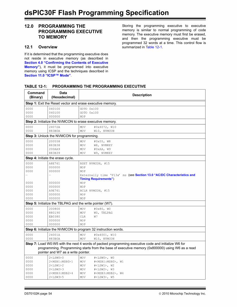
dsPIC30F Flash Programming Specification
12.0 PROGRAMMING THE PROGRAMMING EXECUTIVE TO MEMORY
12.1 OverviewIf it is determined that the programming executive does not reside in executive memory (as described in Section 4.0 “Confirming the Contents of Executive Memory”), it must be programmed into executive memory using ICSP and the techniques described in Section 11.0 “ICSP™ Mode”.
Storing the programming executive to executive memory is similar to normal programming of code memory. The executive memory must first be erased, and then the programming executive must be programmed 32 words at a time. This control flow is summarized in Table 12-1.
TABLE 12-1: PROGRAMMING THE PROGRAMMING EXECUTIVE Command(Binary)
Data(Hexadecimal) Description
Step 1: Exit the Reset vector and erase executive memory.000000000000
040100040100000000
GOTO 0x100GOTO 0x100NOP
Step 2: Initialize the NVMCON to erase executive memory.00000000
24072A 883B0A
MOV #0x4072, W10 MOV W10, NVMCON
Step 3: Unlock the NVMCON for programming.0000000000000000
200558 883B38 200AA9 883B39
MOV #0x55, W8 MOV W8, NVMKEYMOV #0xAA, W9 MOV W9, NVMKEY
Step 4: Initiate the erase cycle.000000000000—
00000000000000000000
A8E761 000000000000 —
000000000000A9E761000000000000
BSET NVMCON, #15 NOPNOPExternally time ‘P13a’ ms (see Section 13.0 “AC/DC Characteristics and Timing Requirements”)NOPNOPBCLR NVMCON, #15NOPNOP
Step 5: Initialize the TBLPAG and the write pointer (W7).00000000000000000000
200800 880190 EB0380000000000000
MOV #0x80, W0 MOV W0, TBLPAG CLR W7 NOPNOP
Step 6: Initialize the NVMCON to program 32 instruction words.00000000
24001A883B0A
MOV #0x4001, W10 MOV W10, NVMCON
Step 7: Load W0:W5 with the next 4 words of packed programming executive code and initialize W6 for programming. Programming starts from the base of executive memory (0x800000) using W6 as a read pointer and W7 as a write pointer.
000000000000000000000000
2<LSW0>0 2<MSB1:MSB0>1 2<LSW1>2 2<LSW2>3 2<MSB3:MSB2>4 2<LSW3>5
MOV #<LSW0>, W0 MOV #<MSB1:MSB0>, W1 MOV #<LSW1>, W2 MOV #<LSW2>, W3 MOV #<MSB3:MSB2>, W4 MOV #<LSW3>, W5
DS70102K-page 54 © 2010 Microchip Technology Inc.
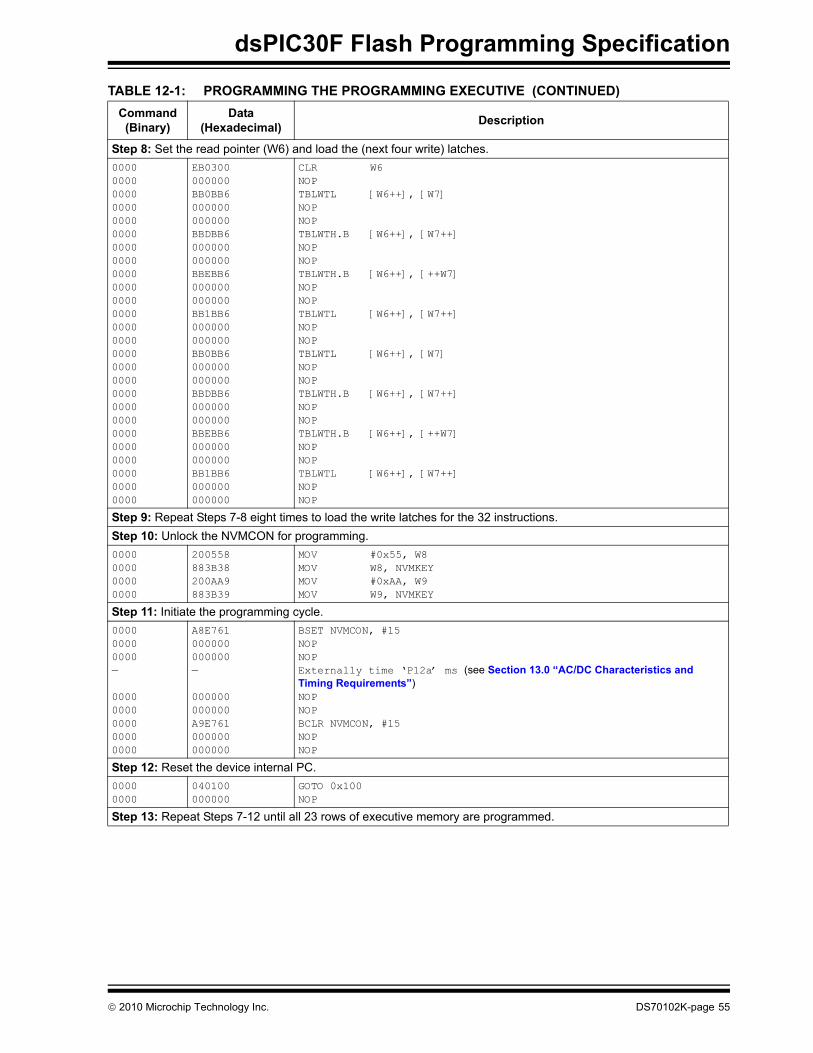
dsPIC30F Flash Programming Specification
Step 8: Set the read pointer (W6) and load the (next four write) latches.00000000000000000000000000000000000000000000000000000000000000000000000000000000000000000000000000000000
EB0300000000BB0BB6 000000000000 BBDBB6 000000000000 BBEBB6 000000000000 BB1BB6 000000000000 BB0BB6 000000 000000BBDBB6 000000 000000BBEBB6 000000 000000BB1BB6 000000000000
CLR W6NOPTBLWTL [W6++], [W7] NOPNOPTBLWTH.B [W6++], [W7++] NOPNOPTBLWTH.B [W6++], [++W7] NOPNOPTBLWTL [W6++], [W7++] NOPNOPTBLWTL [W6++], [W7] NOPNOPTBLWTH.B [W6++], [W7++] NOPNOPTBLWTH.B [W6++], [++W7] NOPNOPTBLWTL [W6++], [W7++] NOPNOP
Step 9: Repeat Steps 7-8 eight times to load the write latches for the 32 instructions.Step 10: Unlock the NVMCON for programming.0000000000000000
200558 883B38 200AA9 883B39
MOV #0x55, W8 MOV W8, NVMKEYMOV #0xAA, W9 MOV W9, NVMKEY
Step 11: Initiate the programming cycle.000000000000—
00000000000000000000
A8E761 000000000000 —
000000000000A9E761000000000000
BSET NVMCON, #15 NOPNOPExternally time ‘P12a’ ms (see Section 13.0 “AC/DC Characteristics and Timing Requirements”)NOPNOPBCLR NVMCON, #15NOPNOP
Step 12: Reset the device internal PC.00000000
040100 000000
GOTO 0x100 NOP
Step 13: Repeat Steps 7-12 until all 23 rows of executive memory are programmed.
TABLE 12-1: PROGRAMMING THE PROGRAMMING EXECUTIVE (CONTINUED)Command(Binary)
Data(Hexadecimal) Description
© 2010 Microchip Technology Inc. DS70102K-page 55
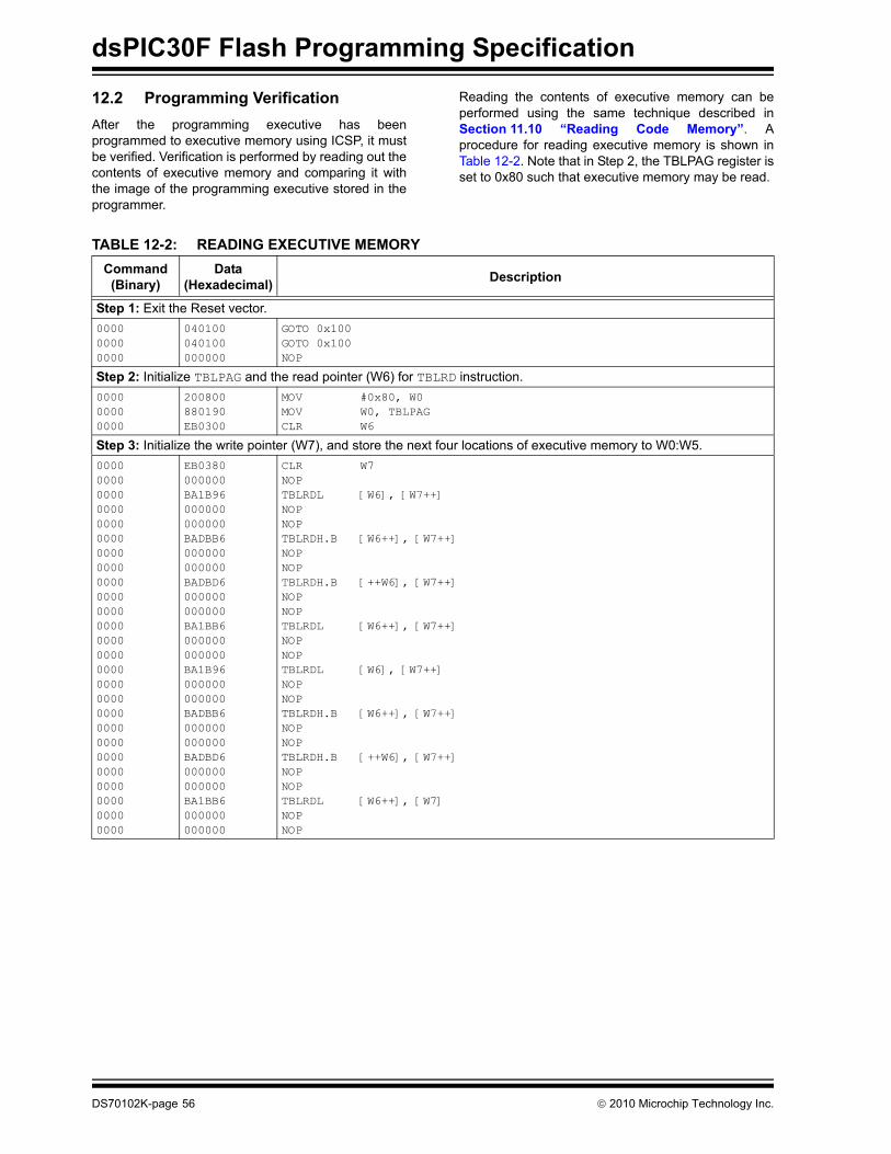
dsPIC30F Flash Programming Specification
12.2 Programming Verification After the programming executive has been programmed to executive memory using ICSP, it must be verified. Verification is performed by reading out the contents of executive memory and comparing it with the image of the programming executive stored in the programmer.
Reading the contents of executive memory can be performed using the same technique described in Section 11.10 “Reading Code Memory”. A procedure for reading executive memory is shown in Table 12-2. Note that in Step 2, the TBLPAG register is set to 0x80 such that executive memory may be read.
TABLE 12-2: READING EXECUTIVE MEMORY Command(Binary)
Data(Hexadecimal) Description
Step 1: Exit the Reset vector.000000000000
040100040100000000
GOTO 0x100GOTO 0x100NOP
Step 2: Initialize TBLPAG and the read pointer (W6) for TBLRD instruction.000000000000
200800880190EB0300
MOV #0x80, W0 MOV W0, TBLPAGCLR W6
Step 3: Initialize the write pointer (W7), and store the next four locations of executive memory to W0:W5. 00000000000000000000000000000000000000000000000000000000000000000000000000000000000000000000000000000000
EB0380000000BA1B96000000000000BADBB6000000000000BADBD6000000000000BA1BB6000000000000BA1B96000000000000BADBB6000000000000BADBD6000000000000BA1BB6000000000000
CLR W7NOPTBLRDL [W6], [W7++]NOPNOPTBLRDH.B [W6++], [W7++]NOPNOPTBLRDH.B [++W6], [W7++]NOPNOPTBLRDL [W6++], [W7++]NOPNOPTBLRDL [W6], [W7++]NOPNOPTBLRDH.B [W6++], [W7++]NOPNOPTBLRDH.B [++W6], [W7++]NOPNOPTBLRDL [W6++], [W7]NOPNOP
DS70102K-page 56 © 2010 Microchip Technology Inc.

dsPIC30F Flash Programming Specification
Step 4: Output W0:W5 using the VISI register and REGOUT command.000000000001000000000001000000000001000000000001000000000001000000000001
883C20000000—883C21000000—883C22000000—883C23000000—883C24000000—883C25000000—
MOV W0, VISINOPClock out contents of VISI registerMOV W1, VISINOPClock out contents of VISI registerMOV W2, VISINOPClock out contents of VISI registerMOV W3, VISINOPClock out contents of VISI registerMOV W4, VISINOPClock out contents of VISI registerMOV W5, VISINOPClock out contents of VISI register
Step 5: Reset the device internal PC.00000000
040100 000000
GOTO 0x100 NOP
Step 6: Repeat Steps 3-5 until all 736 instruction words of executive memory are read.
TABLE 12-2: READING EXECUTIVE MEMORY (CONTINUED)Command(Binary)
Data(Hexadecimal) Description
© 2010 Microchip Technology Inc. DS70102K-page 57
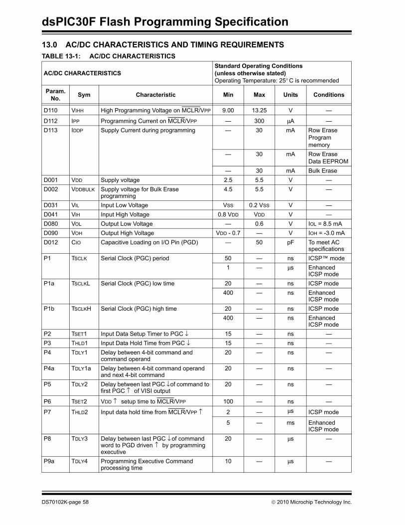
dsPIC30F Flash Programming Specification
13.0 AC/DC CHARACTERISTICS AND TIMING REQUIREMENTSTABLE 13-1: AC/DC CHARACTERISTICS
AC/DC CHARACTERISTICSStandard Operating Conditions (unless otherwise stated)Operating Temperature: 25° C is recommended
Param. No. Sym Characteristic Min Max Units Conditions
D110 VIHH High Programming Voltage on MCLR/VPP 9.00 13.25 V —
D112 IPP Programming Current on MCLR/VPP — 300 μA —D113 IDDP Supply Current during programming — 30 mA Row Erase
Program memory
— 30 mA Row Erase Data EEPROM
— 30 mA Bulk EraseD001 VDD Supply voltage 2.5 5.5 V —D002 VDDBULK Supply voltage for Bulk Erase
programming4.5 5.5 V —
D031 VIL Input Low Voltage VSS 0.2 VSS V —D041 VIH Input High Voltage 0.8 VDD VDD V —D080 VOL Output Low Voltage — 0.6 V IOL = 8.5 mAD090 VOH Output High Voltage VDD - 0.7 — V IOH = -3.0 mAD012 CIO Capacitive Loading on I/O Pin (PGD) — 50 pF To meet AC
specificationsP1 TSCLK Serial Clock (PGC) period 50 — ns ICSP™ mode
1 — μs Enhanced ICSP mode
P1a TSCLKL Serial Clock (PGC) low time 20 — ns ICSP mode400 — ns Enhanced
ICSP modeP1b TSCLKH Serial Clock (PGC) high time 20 — ns ICSP mode
400 — ns Enhanced ICSP mode
P2 TSET1 Input Data Setup Timer to PGC ↓ 15 — ns —P3 THLD1 Input Data Hold Time from PGC ↓ 15 — ns —P4 TDLY1 Delay between 4-bit command and
command operand20 — ns —
P4a TDLY1a Delay between 4-bit command operand and next 4-bit command
20 — ns —
P5 TDLY2 Delay between last PGC ↓ of command to first PGC ↑ of VISI output
20 — ns —
P6 TSET2 VDD ↑ setup time to MCLR/VPP 100 — ns —
P7 THLD2 Input data hold time from MCLR/VPP ↑ 2 — μs ICSP mode
5 — ms Enhanced ICSP mode
P8 TDLY3 Delay between last PGC ↓ of command word to PGD driven ↑ by programming executive
20 — μs —
P9a TDLY4 Programming Executive Command processing time
10 — μs —
DS70102K-page 58 © 2010 Microchip Technology Inc.
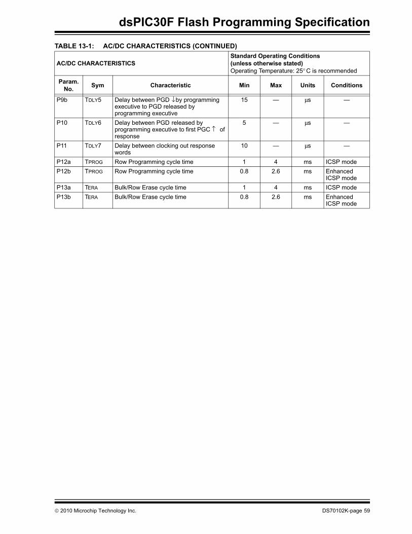
dsPIC30F Flash Programming Specification
P9b TDLY5 Delay between PGD ↓ by programming executive to PGD released by programming executive
15 — μs —
P10 TDLY6 Delay between PGD released by programming executive to first PGC ↑ of response
5 — μs —
P11 TDLY7 Delay between clocking out response words
10 — μs —
P12a TPROG Row Programming cycle time 1 4 ms ICSP modeP12b TPROG Row Programming cycle time 0.8 2.6 ms Enhanced
ICSP modeP13a TERA Bulk/Row Erase cycle time 1 4 ms ICSP modeP13b TERA Bulk/Row Erase cycle time 0.8 2.6 ms Enhanced
ICSP mode
TABLE 13-1: AC/DC CHARACTERISTICS (CONTINUED)
AC/DC CHARACTERISTICSStandard Operating Conditions (unless otherwise stated)Operating Temperature: 25° C is recommended
Param. No. Sym Characteristic Min Max Units Conditions
© 2010 Microchip Technology Inc. DS70102K-page 59
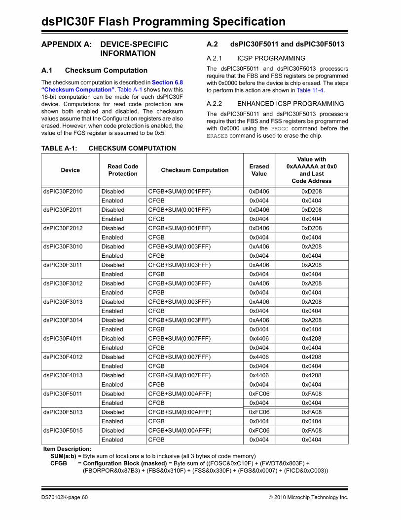
dsPIC30F Flash Programming Specification
APPENDIX A: DEVICE-SPECIFIC INFORMATION
A.1 Checksum ComputationThe checksum computation is described in Section 6.8 “Checksum Computation”. Table A-1 shows how this 16-bit computation can be made for each dsPIC30Fdevice. Computations for read code protection are shown both enabled and disabled. The checksum values assume that the Configuration registers are also erased. However, when code protection is enabled, the value of the FGS register is assumed to be 0x5.
A.2 dsPIC30F5011 and dsPIC30F5013
A.2.1 ICSP PROGRAMMINGThe dsPIC30F5011 and dsPIC30F5013 processors require that the FBS and FSS registers be programmed with 0x0000 before the device is chip erased. The steps to perform this action are shown in Table 11-4.
A.2.2 ENHANCED ICSP PROGRAMMINGThe dsPIC30F5011 and dsPIC30F5013 processors require that the FBS and FSS registers be programmed with 0x0000 using the PROGC command before the ERASEB command is used to erase the chip.
TABLE A-1: CHECKSUM COMPUTATION
Device Read CodeProtection Checksum Computation Erased
Value
Value with0xAAAAAA at 0x0
and LastCode Address
dsPIC30F2010 Disabled CFGB+SUM(0:001FFF) 0xD406 0xD208Enabled CFGB 0x0404 0x0404
dsPIC30F2011 Disabled CFGB+SUM(0:001FFF) 0xD406 0xD208Enabled CFGB 0x0404 0x0404
dsPIC30F2012 Disabled CFGB+SUM(0:001FFF) 0xD406 0xD208Enabled CFGB 0x0404 0x0404
dsPIC30F3010 Disabled CFGB+SUM(0:003FFF) 0xA406 0xA208Enabled CFGB 0x0404 0x0404
dsPIC30F3011 Disabled CFGB+SUM(0:003FFF) 0xA406 0xA208Enabled CFGB 0x0404 0x0404
dsPIC30F3012 Disabled CFGB+SUM(0:003FFF) 0xA406 0xA208Enabled CFGB 0x0404 0x0404
dsPIC30F3013 Disabled CFGB+SUM(0:003FFF) 0xA406 0xA208Enabled CFGB 0x0404 0x0404
dsPIC30F3014 Disabled CFGB+SUM(0:003FFF) 0xA406 0xA208Enabled CFGB 0x0404 0x0404
dsPIC30F4011 Disabled CFGB+SUM(0:007FFF) 0x4406 0x4208Enabled CFGB 0x0404 0x0404
dsPIC30F4012 Disabled CFGB+SUM(0:007FFF) 0x4406 0x4208Enabled CFGB 0x0404 0x0404
dsPIC30F4013 Disabled CFGB+SUM(0:007FFF) 0x4406 0x4208Enabled CFGB 0x0404 0x0404
dsPIC30F5011 Disabled CFGB+SUM(0:00AFFF) 0xFC06 0xFA08Enabled CFGB 0x0404 0x0404
dsPIC30F5013 Disabled CFGB+SUM(0:00AFFF) 0xFC06 0xFA08Enabled CFGB 0x0404 0x0404
dsPIC30F5015 Disabled CFGB+SUM(0:00AFFF) 0xFC06 0xFA08Enabled CFGB 0x0404 0x0404
Item Description:SUM(a:b) = Byte sum of locations a to b inclusive (all 3 bytes of code memory)CFGB = Configuration Block (masked) = Byte sum of ((FOSC&0xC10F) + (FWDT&0x803F) +
(FBORPOR&0x87B3) + (FBS&0x310F) + (FSS&0x330F) + (FGS&0x0007) + (FICD&0xC003))
DS70102K-page 60 © 2010 Microchip Technology Inc.
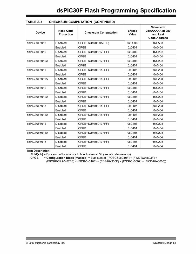
dsPIC30F Flash Programming Specification
dsPIC30F5016 Disabled CFGB+SUM(0:00AFFF) 0xFC06 0xFA08Enabled CFGB 0x0404 0x0404
dsPIC30F6010 Disabled CFGB+SUM(0:017FFF) 0xC406 0xC208Enabled CFGB 0x0404 0x0404
dsPIC30F6010A Disabled CFGB+SUM(0:017FFF) 0xC406 0xC208Enabled CFGB 0x0404 0x0404
dsPIC30F6011 Disabled CFGB+SUM(0:015FFF) 0xF406 0xF208Enabled CFGB 0x0404 0x0404
dsPIC30F6011A Disabled CFGB+SUM(0:015FFF) 0xF406 0xF208Enabled CFGB 0x0404 0x0404
dsPIC30F6012 Disabled CFGB+SUM(0:017FFF) 0xC406 0xC208Enabled CFGB 0x0404 0x0404
dsPIC30F6012A Disabled CFGB+SUM(0:017FFF) 0xC406 0xC208Enabled CFGB 0x0404 0x0404
dsPIC30F6013 Disabled CFGB+SUM(0:015FFF) 0xF406 0xF208Enabled CFGB 0x0404 0x0404
dsPIC30F6013A Disabled CFGB+SUM(0:015FFF) 0xF406 0xF208Enabled CFGB 0x0404 0x0404
dsPIC30F6014 Disabled CFGB+SUM(0:017FFF) 0xC406 0xC208Enabled CFGB 0x0404 0x0404
dsPIC30F6014A Disabled CFGB+SUM(0:017FFF) 0xC406 0xC208Enabled CFGB 0x0404 0x0404
dsPIC30F6015 Disabled CFGB+SUM(0:017FFF) 0xC406 0xC208Enabled CFGB 0x0404 0x0404
TABLE A-1: CHECKSUM COMPUTATION (CONTINUED)
Device Read CodeProtection Checksum Computation Erased
Value
Value with0xAAAAAA at 0x0
and LastCode Address
Item Description:SUM(a:b) = Byte sum of locations a to b inclusive (all 3 bytes of code memory)CFGB = Configuration Block (masked) = Byte sum of ((FOSC&0xC10F) + (FWDT&0x803F) +
(FBORPOR&0x87B3) + (FBS&0x310F) + (FSS&0x330F) + (FGS&0x0007) + (FICD&0xC003))
© 2010 Microchip Technology Inc. DS70102K-page 61
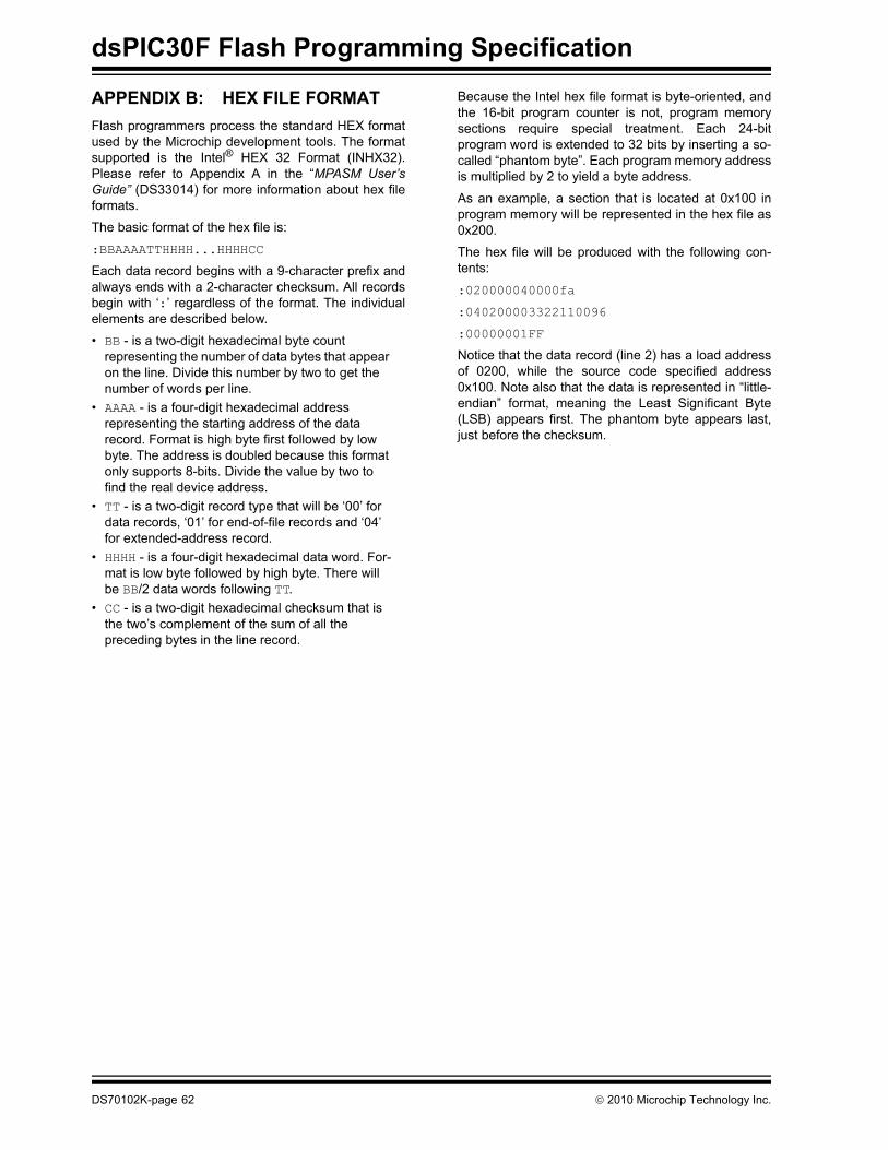
dsPIC30F Flash Programming Specification
APPENDIX B: HEX FILE FORMATFlash programmers process the standard HEX format used by the Microchip development tools. The format supported is the Intel® HEX 32 Format (INHX32). Please refer to Appendix A in the “MPASM User’s Guide” (DS33014) for more information about hex file formats.
The basic format of the hex file is:
:BBAAAATTHHHH...HHHHCC
Each data record begins with a 9-character prefix and always ends with a 2-character checksum. All records begin with ‘:’ regardless of the format. The individual elements are described below.
• BB - is a two-digit hexadecimal byte count representing the number of data bytes that appear on the line. Divide this number by two to get the number of words per line.
• AAAA - is a four-digit hexadecimal address representing the starting address of the data record. Format is high byte first followed by low byte. The address is doubled because this format only supports 8-bits. Divide the value by two to find the real device address.
• TT - is a two-digit record type that will be ‘00’ for data records, ‘01’ for end-of-file records and ‘04’ for extended-address record.
• HHHH - is a four-digit hexadecimal data word. For-mat is low byte followed by high byte. There will be BB/2 data words following TT.
• CC - is a two-digit hexadecimal checksum that is the two’s complement of the sum of all the preceding bytes in the line record.
Because the Intel hex file format is byte-oriented, and the 16-bit program counter is not, program memory sections require special treatment. Each 24-bit program word is extended to 32 bits by inserting a so-called “phantom byte”. Each program memory address is multiplied by 2 to yield a byte address.
As an example, a section that is located at 0x100 in program memory will be represented in the hex file as 0x200.
The hex file will be produced with the following con-tents:
:020000040000fa
:040200003322110096
:00000001FF
Notice that the data record (line 2) has a load address of 0200, while the source code specified address 0x100. Note also that the data is represented in “little-endian” format, meaning the Least Significant Byte(LSB) appears first. The phantom byte appears last, just before the checksum.
DS70102K-page 62 © 2010 Microchip Technology Inc.
dsPIC30F Flash Programming Specification
APPENDIX C: REVISION HISTORYNote: Revision histories were not recorded for
revisions A through H. The previous revision (J), was published in August 2007.
Revision K (November 2010)This version of the document includes the following updates:
• Added Note three to Section 5.2 “Entering Enhanced ICSP Mode”
• Updated the first paragraph of Section 10.0 “Device ID”
• Updated Table 10-1: Device IDs• Removed the VARIANT bit and updated the bit
definition for the DEVID register in Table 10-2: dsPIC30F Device ID Registers
• Removed the VARIANT bit and updated the bit field definition and description for the DEVID register in Table 10-3: Device ID Bits Description
• Updated Note 3 in Section 11.3 “Entering ICSP Mode”
• Updated Step 11 in Table 11-4: Serial Instruction Execution for BUlk Erasing Program Memory (Only in Normal-voltage Systems)
• Updated Steps 5, 12 and 19 in Table 11-5: Serial Instruction Execution for Erasing Program Memory (Either in Low-voltage or Normal-voltage Systems)
• Updated Steps 5, 6 and 8 in Table 11-7: Serial Instruction Execution for Writing Configuration Registers
• Updated Steps 6 and 8 in Table 11-8: Serial Instruction Execution for Writing Code Memory
• Updated Steps 6 and 8 in Table 11-9: Serial Instruction Execution for Writing Data EEPROM
• Updated Entering ICSP™ Mode (see Figure 11-4)• Updated Steps 4 and 11 in Table 12-1:
Programming the Programming Executive• Renamed parameters: P12 to P12a and P13 to
P13a, and added parameters P12b and P13b in Table 13-1: AC/DC Characteristics
© 2010 Microchip Technology Inc. DS70102K-page 63
dsPIC30F Flash Programming Specification
NOTES:
DS70102K-page 64 © 2010 Microchip Technology Inc.

Note the following details of the code protection feature on Microchip devices:• Microchip products meet the specification contained in their particular Microchip Data Sheet.
• Microchip believes that its family of products is one of the most secure families of its kind on the market today, when used in the intended manner and under normal conditions.
• There are dishonest and possibly illegal methods used to breach the code protection feature. All of these methods, to our knowledge, require using the Microchip products in a manner outside the operating specifications contained in Microchip’s Data Sheets. Most likely, the person doing so is engaged in theft of intellectual property.
• Microchip is willing to work with the customer who is concerned about the integrity of their code.
• Neither Microchip nor any other semiconductor manufacturer can guarantee the security of their code. Code protection does not mean that we are guaranteeing the product as “unbreakable.”
Code protection is constantly evolving. We at Microchip are committed to continuously improving the code protection features of our products. Attempts to break Microchip’s code protection feature may be a violation of the Digital Millennium Copyright Act. If such acts allow unauthorized access to your software or other copyrighted work, you may have a right to sue for relief under that Act.
Information contained in this publication regarding device applications and the like is provided only for your convenience and may be superseded by updates. It is your responsibility to ensure that your application meets with your specifications. MICROCHIP MAKES NO REPRESENTATIONS OR WARRANTIES OF ANY KIND WHETHER EXPRESS OR IMPLIED, WRITTEN OR ORAL, STATUTORY OR OTHERWISE, RELATED TO THE INFORMATION, INCLUDING BUT NOT LIMITED TO ITS CONDITION, QUALITY, PERFORMANCE, MERCHANTABILITY OR FITNESS FOR PURPOSE. Microchip disclaims all liability arising from this information and its use. Use of Microchip devices in life support and/or safety applications is entirely at the buyer’s risk, and the buyer agrees to defend, indemnify and hold harmless Microchip from any and all damages, claims, suits, or expenses resulting from such use. No licenses are conveyed, implicitly or otherwise, under any Microchip intellectual property rights.
© 2010 Microchip Technology Inc.
Trademarks
The Microchip name and logo, the Microchip logo, dsPIC, KEELOQ, KEELOQ logo, MPLAB, PIC, PICmicro, PICSTART, PIC32 logo, rfPIC and UNI/O are registered trademarks of Microchip Technology Incorporated in the U.S.A. and other countries.
FilterLab, Hampshire, HI-TECH C, Linear Active Thermistor, MXDEV, MXLAB, SEEVAL and The Embedded Control Solutions Company are registered trademarks of Microchip Technology Incorporated in the U.S.A.
Analog-for-the-Digital Age, Application Maestro, CodeGuard, dsPICDEM, dsPICDEM.net, dsPICworks, dsSPEAK, ECAN, ECONOMONITOR, FanSense, HI-TIDE, In-Circuit Serial Programming, ICSP, Mindi, MiWi, MPASM, MPLAB Certified logo, MPLIB, MPLINK, mTouch, Omniscient Code Generation, PICC, PICC-18, PICDEM, PICDEM.net, PICkit, PICtail, REAL ICE, rfLAB, Select Mode, Total Endurance, TSHARC, UniWinDriver, WiperLock and ZENA are trademarks of Microchip Technology Incorporated in the U.S.A. and other countries.
SQTP is a service mark of Microchip Technology Incorporated in the U.S.A.
All other trademarks mentioned herein are property of their respective companies.
© 2010, Microchip Technology Incorporated, Printed in the U.S.A., All Rights Reserved.
Printed on recycled paper.
ISBN: 978-1-60932-636-4
DS70102K-page 65
Microchip received ISO/TS-16949:2002 certification for its worldwide headquarters, design and wafer fabrication facilities in Chandler and Tempe, Arizona; Gresham, Oregon and design centers in California and India. The Company’s quality system processes and procedures are for its PIC® MCUs and dsPIC® DSCs, KEELOQ® code hopping devices, Serial EEPROMs, microperipherals, nonvolatile memory and analog products. In addition, Microchip’s quality system for the design and manufacture of development systems is ISO 9001:2000 certified.

DS70102K-page 66 © 2010 Microchip Technology Inc.
AMERICASCorporate Office2355 West Chandler Blvd.Chandler, AZ 85224-6199Tel: 480-792-7200 Fax: 480-792-7277Technical Support: http://support.microchip.comWeb Address: www.microchip.comAtlantaDuluth, GA Tel: 678-957-9614 Fax: 678-957-1455BostonWestborough, MA Tel: 774-760-0087 Fax: 774-760-0088ChicagoItasca, IL Tel: 630-285-0071 Fax: 630-285-0075ClevelandIndependence, OH Tel: 216-447-0464 Fax: 216-447-0643DallasAddison, TX Tel: 972-818-7423 Fax: 972-818-2924DetroitFarmington Hills, MI Tel: 248-538-2250Fax: 248-538-2260KokomoKokomo, IN Tel: 765-864-8360Fax: 765-864-8387Los AngelesMission Viejo, CA Tel: 949-462-9523 Fax: 949-462-9608Santa ClaraSanta Clara, CA Tel: 408-961-6444Fax: 408-961-6445TorontoMississauga, Ontario, CanadaTel: 905-673-0699 Fax: 905-673-6509
ASIA/PACIFICAsia Pacific OfficeSuites 3707-14, 37th FloorTower 6, The GatewayHarbour City, KowloonHong KongTel: 852-2401-1200Fax: 852-2401-3431Australia - SydneyTel: 61-2-9868-6733Fax: 61-2-9868-6755China - BeijingTel: 86-10-8528-2100 Fax: 86-10-8528-2104China - ChengduTel: 86-28-8665-5511Fax: 86-28-8665-7889China - ChongqingTel: 86-23-8980-9588Fax: 86-23-8980-9500China - Hong Kong SARTel: 852-2401-1200 Fax: 852-2401-3431China - NanjingTel: 86-25-8473-2460Fax: 86-25-8473-2470China - QingdaoTel: 86-532-8502-7355Fax: 86-532-8502-7205China - ShanghaiTel: 86-21-5407-5533 Fax: 86-21-5407-5066China - ShenyangTel: 86-24-2334-2829Fax: 86-24-2334-2393China - ShenzhenTel: 86-755-8203-2660 Fax: 86-755-8203-1760China - WuhanTel: 86-27-5980-5300Fax: 86-27-5980-5118China - XianTel: 86-29-8833-7252Fax: 86-29-8833-7256China - XiamenTel: 86-592-2388138 Fax: 86-592-2388130China - ZhuhaiTel: 86-756-3210040 Fax: 86-756-3210049
ASIA/PACIFICIndia - BangaloreTel: 91-80-3090-4444 Fax: 91-80-3090-4123India - New DelhiTel: 91-11-4160-8631Fax: 91-11-4160-8632India - PuneTel: 91-20-2566-1512Fax: 91-20-2566-1513Japan - YokohamaTel: 81-45-471- 6166 Fax: 81-45-471-6122Korea - DaeguTel: 82-53-744-4301Fax: 82-53-744-4302Korea - SeoulTel: 82-2-554-7200Fax: 82-2-558-5932 or 82-2-558-5934Malaysia - Kuala LumpurTel: 60-3-6201-9857Fax: 60-3-6201-9859Malaysia - PenangTel: 60-4-227-8870Fax: 60-4-227-4068Philippines - ManilaTel: 63-2-634-9065Fax: 63-2-634-9069SingaporeTel: 65-6334-8870Fax: 65-6334-8850Taiwan - Hsin ChuTel: 886-3-6578-300Fax: 886-3-6578-370Taiwan - KaohsiungTel: 886-7-213-7830Fax: 886-7-330-9305Taiwan - TaipeiTel: 886-2-2500-6610 Fax: 886-2-2508-0102Thailand - BangkokTel: 66-2-694-1351Fax: 66-2-694-1350
EUROPEAustria - WelsTel: 43-7242-2244-39Fax: 43-7242-2244-393Denmark - CopenhagenTel: 45-4450-2828 Fax: 45-4485-2829France - ParisTel: 33-1-69-53-63-20 Fax: 33-1-69-30-90-79Germany - MunichTel: 49-89-627-144-0 Fax: 49-89-627-144-44Italy - Milan Tel: 39-0331-742611 Fax: 39-0331-466781Netherlands - DrunenTel: 31-416-690399 Fax: 31-416-690340Spain - MadridTel: 34-91-708-08-90Fax: 34-91-708-08-91UK - WokinghamTel: 44-118-921-5869Fax: 44-118-921-5820
Worldwide Sales and Service
08/04/10