pic16(l)f184xx programming specificationww1.microchip.com/downloads/en/devicedoc/pic16(l)f184xx...
TRANSCRIPT
PIC16(L)F184XX PIC16(L)F184XX Memory Programming Specification
Overview
The PIC16(L)F184XX Memory Programming Specification describes the programming method for thePIC16(L)F184XX family of 8-bit microcontrollers The programming specification describes theprogramming commands programming algorithms and electrical specifications which are used in thatparticular programming method ldquoAppendix Brdquo contains individual part numbers device identification andchecksum values pinout and packaging information and Configuration Words
Note To enter LVP mode the MSb of the Most Significant nibble must be shifted in first This differsfrom entering the key sequence on some other device families
Related LinksAppendix B Device ID Checksums and Pinout Descriptions
Programming Data Flow
Nonvolatile Memory (NVM) programming data can be supplied by either the high-voltage In-Circuit SerialProgrammingtrade (ICSPtrade) interface or the low-voltage In-Circuit Serial Programmingtrade (ICSPtrade) interfaceData can be programmed into the Program Flash Memory EEPROM dedicated ldquoUser IDrdquo locations andthe Configuration Words
Write andor Erase Selection
Erasing or writing is selected according to the command used to begin operation (see the ldquoProgramVerifyCommandsrdquo section for more details) The terminologies used in this document related to erasingwritingto the Program Flash Memory are defined in the table below
Table 1 Programming Terms
Term Definition
Programmed Cell A memory cell with a logic lsquo0rsquo
Erased Cell A memory cell with a logic lsquo1rsquo
Erase Change memory cell from a lsquo0rsquo to a lsquo1rsquo
Write Change memory cell from a lsquo1rsquo to a lsquo0rsquo
Program Generic erase andor write
Related LinksProgramVerify Commands
copy 2017 Microchip Technology Inc DS40001970A-page 1
1 Erasing MemoryProgram Flash Memory is erased by row or in bulk where lsquobulkrsquo includes many subsets of the total memoryspace The duration of the erase is always determined internally Here lsquorowrsquo refers to the minimum erasablesize and lsquobulkrsquo is one of the many possible subsets of all memory rows All Bulk ICSP Erase commands haveminimum VDD requirements which are higher than the Row Erase and write requirements
Related LinksElectrical Specifications
2 Writing MemoryProgram Flash Memory is written one row at a time while EEPROM is written one byte at a time Multipleload data for NVM commands are used to fill the Program Flash Memoryrsquos row data latches The duration ofthe write is determined either internally or externally
Related LinksElectrical Specifications
3 Multi-Word Programming InterfaceProgram Flash Memory panels include a 32-word (one row) programming interface The row to beprogrammed must first be erased either with a Bulk Erase or a Row Erase
Related LinksElectrical Specifications
Hardware Requirements
1 High-Voltage ICSP ProgrammingIn High-Voltage ICSP mode the device requires two programmable power supplies one for VDD and one forthe MCLRVPP pin
2 Low-Voltage ICSP ProgrammingIn Low-Voltage ICSP mode the device can be programmed using a single VDD source in the operating rangeThe MCLRVPP pin does not have to be brought to a different voltage but can instead be left at the normaloperating voltage
21 Single-Supply ICSP Programming
The LVP Configuration bit enables single-supply (low-voltage) ICSP programming The LVP bit defaults to alsquo1rsquo (enabled) from the factory The LVP bit may only be programmed to lsquo0rsquo by entering the High-Voltage ICSPmode where the MCLRVPP pin is raised to VIHH Once the LVP bit is programmed to a lsquo0rsquo only the High-Voltage ICSP mode is available and only the High-Voltage ICSP mode can be used to program the device
Note
PIC16(L)F184XX
copy 2017 Microchip Technology Inc DS40001970A-page 2
1 The High-Voltage ICSP mode is always available regardless of the state of the LVP bit by applyingVIHH to the MCLRVPP pin
2 While in Low-Voltage ICSP mode MCLR is always enabled regardless of the MCLRE bit and the portpin can no longer be used as a general purpose input
Pin Utilization
Five pins are needed for ICSP programming The pins are listed in the table below
Table 1 Pin Descriptions during Programming
Pin NameDuring Programming
Function Pin Type Pin Description
ICSPCLK ICSPCLK I Clock Input ndash Schmitt Trigger Input
ICSPDAT ICSPDAT IO Data InputOutput ndash Schmitt Trigger Input
MCLRVPP ProgramVerify mode I(1) Program Mode Select
VDD VDD P Power Supply
VSS VSS P Ground
Legend I = Input O = Output P = Power
Note 1 The programming high voltage is internally generated To activate the ProgramVerify mode high
voltage needs to be applied to the MCLR input Since the MCLR is used for a level source MCLR doesnot draw any significant current
Related LinksProgramming Pin Locations by Package Type
PIC16(L)F184XX
copy 2017 Microchip Technology Inc DS40001970A-page 3
Table of Contents
Overview1
Programming Data Flow1
Write andor Erase Selection11 Erasing Memory 22 Writing Memory 23 Multi-Word Programming Interface 2
Hardware Requirements21 High-Voltage ICSP Programming22 Low-Voltage ICSP Programming2
Pin Utilization3
1 Memory Map611 Program Memory Mapping612 User ID Location713 DeviceRevision ID714 Configuration Words1015 Device Information Area2116 Device Configuration Information21
2 Programming Algorithms 2221 ProgramVerify Mode2222 Programming Algorithms3123 Code Protection3724 Hex File Usage3725 Electrical Specifications38
3 Appendix A Revision History (122017)41
4 Appendix B Device ID Checksums and Pinout Descriptions4241 Device IDs and Checksums 4242 Example Checksum Computed with Program Code Protection Disabled Blank Device4243 Example Checksum Computed with Program Code Protection Disabled 00AAh at First and
Last Address 4344 Example Checksum Computed with Program Code Protection Enabled Blank Device4445 Example Checksum Computed with Program Code Protection Enabled 00AAh at First and
Last Address 4446 Programming Pin Locations by Package Type45
5 Appendix C Device Configuration Information (DCI) 47
6 Appendix D Device Information Area (DIA) 48
PIC16(L)F184XX
copy 2017 Microchip Technology Inc DS40001970A-page 4
The Microchip Web Site 49
Customer Change Notification Service49
Customer Support 49
Microchip Devices Code Protection Feature 49
Legal Notice50
Trademarks 50
Quality Management System Certified by DNV51
Worldwide Sales and Service52
PIC16(L)F184XX
copy 2017 Microchip Technology Inc DS40001970A-page 5
1 Memory Map
11 Program Memory Mapping
0000h 0000h
0FFFh 0FFFh
1FFFh 1FFFh
3FFFh 3FFFh
7FFFh 7FFFh8000h 8000h
8003h 8003h8004h 8004h8005h 8005h8006h 8006h8007h 8007h800Bh 800Bh800Ch 800Ch
80FFh 80FFh8100h 8100h811Fh 811Fh8120h 8120h
81FFh 81FFh8200h 8200h821Fh 821Fh8220h 8220hEFFFh EFFFhF000h F000hF0FFh F0FFhF100h F100hFFFFh FFFFh
Reserved
EEPROM
Reserved
Program Flash Memory
Program Flash Memory
Program Flash Memory
Unimplemented(4)
Unimplemented(4)
Unimplemented(4)
PClt150gt(5) PClt150gt(5) PClt150gt(5)
Stack(1) (16 levels)
Configuration Words 1-5(2)
Reserved
Device Information Area (DIA)(2)
Reserved
Device Configuration Information (DCI)(2)
User IDs(2)
ReservedRevision ID(23)
Device ID(23)
PIC16(L)F18424 PIC16(L)F18444
(4k)
PIC16(L)F18425 PIC16(L)F18445 PIC16(L)F18455
(8k)
PIC16(L)F18426 PIC16(L)F18446 PIC16(L)F18456
(16k)
Stack(1) (16 levels) Stack(1) (16 levels)
PIC16(L)F184XXMemory Map
copy 2017 Microchip Technology Inc DS40001970A-page 6
Note 1 The stack is a separate SRAM panel apart from all user memory panels2 Not code-protected3 Device Configuration Information DeviceRevision IDs are hard-coded in silicon4 The addresses do not roll over The region is read as lsquo0rsquo5 For the purposes of instruction fetching during program execution only 15 bits (PClt140gt) are
used However for the purposes of nonvolatile memory reading and writing through ICSPtrade
programming operations the PC uses all16 bits (PClt150gt) and the ldquoLoad PC Addressrdquo commandrequires a full 16-bit data payload
12 User ID LocationA user may store identification information (User ID) in four designated locations The User ID locationsare mapped to 8000h-8003h Each location is 14 bits in length Code protection has no effect on thesememory locations Each location may be read with code protection enabled or disabled
13 DeviceRevision IDThe 14 bits Device ID word is located at 0x8006 and the 14 bits Revision ID is located at 0x8005 Theselocations are read-only and cannot be erased or modified
131 Register Summary - Device and Revision
Offset Name Bit Pos
0x8005 REVISION ID70 MJRREV[10] MNRREV[50]
138 1 0 MJRREV[52]
0x8006 DEVICE ID70 DEV[70]
138 1 1 DEV[118]
132 Register Definitions Device and Revision
PIC16(L)F184XXMemory Map
copy 2017 Microchip Technology Inc DS40001970A-page 7
1321 DEVICE ID
Name DEVICE IDOffset 0x8006
Device ID Register
Bit 15 14 13 12 11 10 9 8 1 1 DEV[118]
Access R R R R R R Reset
Bit 7 6 5 4 3 2 1 0 DEV[70]
Access R R R R R R R R Reset
Bit 13 ndash 1These bit must be lsquo1rsquo to be distinguishable from the previous Device ID scheme
Bit 12 ndash 1These bit must be lsquo1rsquo to be distinguishable from the previous Device ID scheme
Bits 110 ndash DEV[110]Device ID bits
Device Device ID
PIC16F18424 30CA
PIC16LF18424 30CB
PIC16F18425 30CC
PIC16LF18425 30CD
PIC16F18426 30D2
PIC16LF18426 30D3
PIC16F18444 30CE
PIC16LF18444 30CF
PIC16F18445 30D0
PIC16LF18445 30D1
PIC16F18446 30D4
PIC16LF18446 30D5
PIC16F18455 30D7
PIC16LF18455 30D8
PIC16F18456 30D9
PIC16LF18456 30DA
PIC16(L)F184XXMemory Map
copy 2017 Microchip Technology Inc DS40001970A-page 8
Related LinksDevice IDs and Checksums
PIC16(L)F184XXMemory Map
copy 2017 Microchip Technology Inc DS40001970A-page 9
1322 REVISION ID
Name REVISION IDOffset 0x8005
Revision ID Register
Bit 15 14 13 12 11 10 9 8 1 0 MJRREV[52]
Access R R R R R R Reset 1 0
Bit 7 6 5 4 3 2 1 0 MJRREV[10] MNRREV[50]
Access R R R R R R R R Reset
Bit 13 ndash 1 Read as lsquo1rsquoThese bits are fixed with value lsquo1rsquo for all devices in this family
Bit 12 ndash 0 Read as lsquo0rsquoThese bits are fixed with value lsquo0rsquo for all devices in this family
Bits 116 ndash MJRREV[50] Major Revision ID bitsThese bits are used to identify a major revision
Bits 50 ndash MNRREV[50] Minor Revision ID bitsThese bits are used to identify a minor revision
14 Configuration WordsThe devices have five Configuration Words starting at address 8007h through 800Bh The Configurationbits establish configuration values prior to the execution of any software Configuration bits enable ordisable device-specific features
In terms of programming these important Configuration bits should be considered1 LVP Low-Voltage Programming Enable Bit
ndash 1 = ON ndash Low-Voltage Programming is enabled MCLRVPP pin function is MCLR MCLREConfiguration bit is ignored
ndash 0 = OFF ndash HV on MCLRVPP must be used for programming2 CP User Nonvolatile Memory (NVM) Program Memory Code Protection bit
ndash 1 = OFF ndash User NVM code protection disabledndash 0 = ON ndash User NVM code protection enabled
Related LinksLow-Voltage Programming (LVP) ModeCode Protection
PIC16(L)F184XXMemory Map
copy 2017 Microchip Technology Inc DS40001970A-page 10
141 Register Summary - Configuration Words
Offset Name Bit Pos
0x8007 CONFIG170 RSTOSC[20] FEXTOSC[20]
138 FCMEN CSWEN CLKOUTEN
0x8008 CONFIG270 BOREN LPBOREN PWRTS[10] MCLRE
138 DEBUG STVREN PPS1WAY ZCDDIS BORV
0x8009 CONFIG370 WDTE[10] WDTCPS[40]
138 WDTCCS[20] WDTCWS[20]
0x800A CONFIG470 WRTAPP SAFEN BBEN BBSIZE[20]
138 LVP WRTSAF WRTD WRTC WRTB
0x800B CONFIG570 CP
138
142 Register Definitions Configuration Words
PIC16(L)F184XXMemory Map
copy 2017 Microchip Technology Inc DS40001970A-page 11
1421 CONFIG1
Name CONFIG1Offset 0x8007
Configuration word 1
Oscillators
Bit 15 14 13 12 11 10 9 8 FCMEN CSWEN CLKOUTEN
Access RP U RP U U RP Reset 1 1 1 1 1 1
Bit 7 6 5 4 3 2 1 0 RSTOSC[20] FEXTOSC[20]
Access U RP RP RP U RP RP RP Reset 1 1 1 1 1 1 1 1
Bit 13 ndash FCMEN Fail-Safe Clock Monitor Enable bit
Value Description1 FSCM timer enabled0 FSCM timer disabled
Bit 11 ndash CSWEN Clock Switch Enable bit
Value Description1 Writing to NOSC and NDIV is allowed0 The NOSC and NDIV bits cannot be changed by user software
Bit 8 ndash CLKOUTEN Clock Out Enable bit
Value Condition Description1 If FEXTOSC = EC (high mid or low) or Not
EnabledCLKOUT function is disabled IO or oscillatorfunction on OSC2
0 If FEXTOSC = EC (high mid or low) or NotEnabled
CLKOUT function is enabled FOSC4 clockappears at OSC2
Otherwise This bit is ignored
Bits 64 ndash RSTOSC[20] Power-up Default Value for COSC bitsThis value is the Reset default value for COSC and selects the oscillator first used by user softwareRefer to COSC operation
Value Description111 EXTOSC operating per FEXTOSC bits110 HFINTOSC (1 MHz) with OSCFRQ = lsquo010rsquo (4 MHz) and CDIV = lsquo0010rsquo (41)101 LFINTOSC100 SOSC011 Reserved010 EXTOSC with 4x PLL with EXTOSC operating per FEXTOSC bits
PIC16(L)F184XXMemory Map
copy 2017 Microchip Technology Inc DS40001970A-page 12
Value Description001 HFINTOSC with 2x PLL (32 MHz) with OSCFRQ = lsquo101rsquo (16 MHz) and CDIV = lsquo0000rsquo (11)000 Reserved
Bits 20 ndash FEXTOSC[20] FEXTOSC External Oscillator Mode Selection bits
Value Description111 ECH (External Clock) above 8 MHz110 ECM (External Clock) for 100 kHz to 8 MHz101 ECL (External Clock) below 100 kHz100 Oscillator not enabled011 Reserved (do not use)010 HS (Crystal oscillator) above 4 MHz001 XT (Crystal oscillator) above 100 kHz below 4 MHz000 LP (crystal oscillator) optimized for 32768 kHz
PIC16(L)F184XXMemory Map
copy 2017 Microchip Technology Inc DS40001970A-page 13
1422 CONFIG2
Name CONFIG2Offset 0x8008
Configuration Word 2
Supervisor
Bit 15 14 13 12 11 10 9 8 DEBUG STVREN PPS1WAY ZCDDIS BORV
Access RP RP RP RP RP U Reset 1 1 1 1 1 1
Bit 7 6 5 4 3 2 1 0 BOREN[10] LPBOREN PWRTS[10] MCLRE
Access RP RP RP U U RP RP RP Reset 1 1 1 1 1 1 1 1
Bit 13 ndash DEBUG Debugger Enable bit(1)
Value Description1 Background debugger disabled0 Background debugger enabled
Bit 12 ndash STVREN Stack OverflowUnderflow Reset Enable bit
Value Description1 Stack Overflow or Underflow will cause a Reset0 Stack Overflow or Underflow will not cause a Reset
Bit 11 ndash PPS1WAY PPSLOCKED bit One-Way Set Enable bit
Value Description1 The PPSLOCKED bit can be cleared and set only once PPS registers remain locked after
one clearset cycle0 The PPSLOCKED bit can be set and cleared repeatedly (subject to the unlock sequence)
Bit 10 ndash ZCDDIS ZCD Disable bit
Value Description1 ZCD disabled ZCD can be enabled by setting the ZCDSEN bit of the ZCDCON register0 ZCD always enabled ZCDSEN bit is ignored
Bit 9 ndash BORV Brown-out Reset Voltage Selection bit
Value Description1 Brown-out Reset voltage (VBOR) set to lower trip point level0 Brown-out Reset voltage (VBOR) set to higher trip point level
Bits 76 ndash BOREN[10] Brown-out Reset Enable bitsWhen enabled Brown-out Reset Voltage (VBOR) is set by BORV bit
PIC16(L)F184XXMemory Map
copy 2017 Microchip Technology Inc DS40001970A-page 14
Value Description11 Brown-out Reset enabled SBOREN bit is ignored10 Brown-out Reset enabled while running disabled in Sleep SBOREN is ignored01 Brown-out Reset enabled according to SBOREN00 Brown-out Reset disabled
Bit 5 ndash LPBOREN Low-Power BOR Enable bit
Value Description1 Low-Power Brown-out Reset is disabled0 Low-Power Brown-out Reset is enabled
Bits 21 ndash PWRTS[10] Power-up Timer Selection bits
Value Description11 PWRT disabled10 PWRT set at 64 ms01 PWRT set at 16 ms00 PWRT set at 1 ms
Bit 0 ndash MCLRE Master Clear (MCLR) Enable bit
Value Condition DescriptionIf LVP = 1 RE3 pin function is MCLR (it will reset the device when driven low)
1 If LVP = 0 MCLR pin is MCLR (it will reset the device when driven low)0 If LVP = 0 MCLR pin function is port defined function
Note 1 The DEBUG bit in Configuration Words is managed automatically by device development tools
including debuggers and programmers For normal device operation this bit should be maintainedas a lsquo1rsquo
PIC16(L)F184XXMemory Map
copy 2017 Microchip Technology Inc DS40001970A-page 15
1423 CONFIG3
Name CONFIG3Offset 0x8009
Configuration Word 3
Windowed Watchdog Timer
Bit 15 14 13 12 11 10 9 8 WDTCCS[20] WDTCWS[20]
Access RP RP RP RP RP RP Reset 1 1 1 1 1 1
Bit 7 6 5 4 3 2 1 0 WDTE[10] WDTCPS[40]
Access U RP RP RP RP RP RP RP Reset 1 1 1 1 1 1 1 1
Bits 1311 ndash WDTCCS[20] WDT Input Clock Selector bits
Value Description111 Software Control110 to011
Reserved
010 Reserved (no clock)32 kHz SOSC001 WDT reference clock is the 3125 kHz HFINTOSC (MFINTOSC) output000 WDT reference clock is the 310 kHz LFINTOSC
Bits 108 ndash WDTCWS[20] WDT Window Select bits
WDTCWS
WDTCON1 [WINDOW] at PORSoftwarecontrol ofWINDOW
Keyed accessrequiredValue
Window delayPercent of
time
Windowopening
Percent oftime
111 111 na 100 Yes No
110 110 na 100
No Yes
101 101 25 75
100 100 375 625
011 011 50 50
010 010 625 375
001 001 75 25
000 000 875 125
Bits 65 ndash WDTE[10] WDT Operating Mode bits
PIC16(L)F184XXMemory Map
copy 2017 Microchip Technology Inc DS40001970A-page 16
Value Description11 WDT enabled regardless of Sleep SEN is ignored10 WDT enabled while Sleep = 0 suspended when Sleep = 1 SEN bit is ignored01 WDT enableddisabled by SEN bit00 WDT disabled SEN bit is ignored
Bits 40 ndash WDTCPS[40] WDT Period Select bits
WDTCPSWDTCON0[WDTPS] at POR
Software Control of WDTPSValue Divider Ratio
Typical Time Out(FIN = 31 kHz)
11111 01011 165536 216 2s Yes
11110
10011
11110
10011132 25 1 ms No
10010 10010 18388608 223 256s
No
10001 10001 14194304 222 128s
10000 10000 12097152 221 64s
01111 01111 11048576 220 32s
01110 01110 1524299 219 16s
01101 01101 1262144 218 8s
01100 01100 1131072 217 4s
01011 01011 165536 216 2s
01010 01010 132768 215 1s
01001 01001 116384 214 512 ms
01000 01000 18192 213 256 ms
00111 00111 14096 212 128 ms
00110 00110 12048 211 64 ms
00101 00101 11024 210 32 ms
00100 00100 1512 29 16 ms
00011 00011 1256 28 8 ms
00010 00010 1128 27 4 ms
00001 00001 164 26 2 ms
00000 00000 132 25 1 ms
PIC16(L)F184XXMemory Map
copy 2017 Microchip Technology Inc DS40001970A-page 17
1424 CONFIG4
Name CONFIG4Offset 0x800A
Configuration Word 4
Memory Write Protection
Bit 15 14 13 12 11 10 9 8 LVP WRTSAF WRTD WRTC WRTB
Access RW U RW RW RW RW Reset 1 1 1 1 1 1
Bit 7 6 5 4 3 2 1 0 WRTAPP SAFEN BBEN BBSIZE[20]
Access RW U U RW RW RW RW RW Reset 1 1 1 1 1 0 0 1
Bit 13 ndash LVP Low-Voltage Programming Enable bitThe LVP bit cannot be written (to zero) while operating from the LVP programming interface The purposeof this rule is to prevent the user from dropping out of LVP mode while programming from LVP mode oraccidentally eliminating LVP mode from the Configuration state
The preconditioned (erased) state for this bit is critical
Value Description1 Low-voltage programming enabled MCLRVPP pin function is MCLR MCLRE Configuration
bit is ignored0 HV on MCLRVPP must be used for programming
Bit 11 ndash WRTSAF Storage Area Flash Write Protection bit(1)
Value Description1 SAF NOT write-protected0 SAF write-protected
Bit 10 ndash WRTD Data EEPROM Write Protection bit(1)
Value Description1 Data EEPROM NOT write-protected0 Data EEPROM write-protected
Bit 9 ndash WRTC Configuration Register Write Protection bit(1)
Value Description1 Configuration Registers NOT write-protected0 Configuration Registers write-protected
Bit 8 ndash WRTB Boot Block Write Protection bit(1)
PIC16(L)F184XXMemory Map
copy 2017 Microchip Technology Inc DS40001970A-page 18
Value Description1 Boot Block NOT write-protected0 Boot Block write-protected
Bit 7 ndash WRTAPP Application Block Write Protection bit(1)
Value Description1 Application Block NOT write-protected0 Application Block write-protected
Bit 4 ndash SAFEN SAF Enable bit(1)
Value Description1 SAF disabled0 SAF enabled
Bit 3 ndash BBEN Boot Block Enable bit(1)
Value Description1 Boot Block disabled0 Boot Block enabled
Bits 20 ndash BBSIZE[20] Boot Block Size Selection bitsBBSIZE is used only when BBEN = 0BBSIZE bits can only be written while BBEN = 1 after BBEN = 0 BBSIZ is write-protected
Table 1-1 Boot Block Size Bits
BBEN BBSIZEActual Boot Block Size User Program Memory
Size (words)Last Boot
Block MemoryAccess4k 8k 16k
1 xxx 0 0 0 mdash
0 111 512 512 512 01FFh
0 110 1024 1024 1024 03FFh
0 101
2048
2048 2048 07FFh
0 100
4096
4096 0FFFh
0 011
8192 1FFFh0 010
0 001
0 000
Note The maximum boot block size is half the user program memory size All selections higher thanthe maximum are set to half size For example all BBSIZE = 000 - 100 produce a boot block size of 4kW on a 8 kW device
Note
PIC16(L)F184XXMemory Map
copy 2017 Microchip Technology Inc DS40001970A-page 19
1 Bits are implemented as sticky bits Once protection is enabled it can only be reset through a BulkErase
PIC16(L)F184XXMemory Map
copy 2017 Microchip Technology Inc DS40001970A-page 20
1425 CONFIG5
Name CONFIG5Offset 0x800B
Configuration Word 5
Code Protection
Bit 15 14 13 12 11 10 9 8
Access U U U U U U Reset 1 1 1 1 1 1
Bit 7 6 5 4 3 2 1 0 CP
Access U U U U U U U RP Reset 1 1 1 1 1 1 1 1
Bit 0 ndash CP Program Flash Memory Code Protection bit
Value Description1 Program Flash Memory code protection disabled0 Program Flash Memory code protection enabled
15 Device Information AreaThe Device Information Area (DIA) is a dedicated region in the Program Flash Memory The data ismapped from 8100h to 811Fh These locations are read-only and cannot be erased or modified The DIAholds the calibration data for the temperature indicator module and the FVR voltages which are useful fortemperature sensing applications and calibration
Related LinksAppendix D Device Information Area (DIA)
16 Device Configuration InformationThe Device Configuration Information (DCI) is a dedicated region in the Program Flash Memory mappedfrom 8200h to 821Fh The data stored in the DCI memory is hard-coded into the device duringmanufacturing The DCI holds information about the device which is useful for programming andbootloaders These locations are read-only and cannot be erased or modified For more information referto the product-specific data sheet
Related LinksAppendix C Device Configuration Information (DCI)
PIC16(L)F184XXMemory Map
copy 2017 Microchip Technology Inc DS40001970A-page 21
2 Programming Algorithms
21 ProgramVerify ModeIn ProgramVerify mode the program memory and the configuration memory can be accessed andprogrammed in serial fashion ICSPDAT and ICSPCLK are used for the data and the clock respectivelyAll commands and data words are transmitted MSb first Data changes on the rising edge of theICSPCLK and is latched on the falling edge In ProgramVerify mode both the ICSPDAT and ICSPCLKare Schmitt Trigger inputs The sequence that enters the device into ProgramVerify mode places all otherlogic into the Reset state Upon entering ProgramVerify mode all IOs are automatically configured ashigh-impedance inputs On entering the ProgramVerify mode the address is cleared
211 High-Voltage ProgramVerify Mode Entry and Exit
There are two different methods of entering ProgramVerify mode via high voltagebull VPP ndash First Entry modebull VDD ndash First Entry mode
2111 VPP ndash First Entry Mode
To enter ProgramVerify mode via the VPP-First mode the following sequence must be followed1 Hold ICSPCLK and ICSPDAT low All other pins should be unpowered2 Raise the voltage on MCLR from 0V to VIHH3 Raise the voltage on VDD from 0V to the desired operating voltage
The VPP-first entry prevents the device from executing code prior to entering ProgramVerify mode Forexample when the Configuration Word has MCLR disabled (MCLRE = 0) the Power-up Timer isdisabled (PWRTS = 0) the internal oscillator is selected (FOSC = 100) and ICSPDAT and ICSPCLK aredriven by the user application the device will execute code and may drive the ICSPDAT and ISCPCLKIO pins Since code execution may prevent first entry VPP-First Entry mode is strongly recommended asit prevents user code from changing EEPROM contents or driving pins to affect Test mode entry
Related LinksProgramVerify Mode Exit
2112 VDD ndash First Entry ModeTo enter ProgramVerify mode via the VDD-First mode the following sequence must be followed
1 Hold ICSPCLK and ICSPDAT low2 Raise the voltage on VDD from 0V to the desired operating voltage3 Raise the voltage on MCLR from VDD or below to VIHH
The VDD-First mode is useful when programming the device when VDD is already applied for it is notnecessary to disconnect VDD to enter ProgramVerify mode During this cycle any executing code will beinterrupted and halted
Related LinksProgramVerify Mode Exit
PIC16(L)F184XXProgramming Algorithms
copy 2017 Microchip Technology Inc DS40001970A-page 22
2113 ProgramVerify Mode ExitTo exit ProgramVerify mode lower MCLR from VIHH to VIL VDD-First Entry mode should use VDD-LastExit mode (see Figure 2-1) VPP-First Entry mode should use VPP-Last Exit mode (see Figure 2-2)
Figure 2-1 Programming Entry and Exit Modes ndash VPP First and LastPROGRAMMING MODE ENTRY ndash EXIT
VPP LAST
TEXIT
PROGRAMMING MODE ENTRY ndash ENTRY VPP FIRST
TENTS TENTH
VDD
VIHH
VPP
ICSPDAT
ICSPCLK
VIL
Figure 2-2 Programming Entry and Exit Modes ndash VDD First and LastPROGRAMMING MODE ENTRY ndash ENTRY
VDD FIRST
PROGRAMMING MODE ENTRY ndash EXIT VDD LAST
TENTS TENTH
VDD
VIHH
VPP
ICSPDAT
ICSPCLK
VIL
TEXIT
212 Low-Voltage Programming (LVP) ModeThe Low-Voltage Programming mode allows the devices to be programmed using VDD only without highvoltage When the LVP bit of the Configuration Word 4 register is set to lsquo1rsquo the low-voltage ICSPprogramming entry is enabled To disable the Low-Voltage ICSP mode the LVP bit must be programmedto lsquo0rsquo This can only be done while in the High-Voltage Entry mode
Entry into the Low-Voltage ICSP ProgramVerify mode requires the following steps1 MCLR is brought to VIL
PIC16(L)F184XXProgramming Algorithms
copy 2017 Microchip Technology Inc DS40001970A-page 23
2 A 32-bit key sequence is presented on ICSPDAT The LSb of the pattern is a ldquodonrsquot care xrdquo TheProgramVerify mode entry pattern detect hardware verifies only the first 31 bits of the sequenceand the last clock is required to activate the ProgramVerify mode
The key sequence is a specific 32-bit pattern 32rsquoh4d434850 (more easily remembered as MCHP inASCII) The device will enter ProgramVerify mode only if the sequence is valid The Most Significant bitof the Most Significant nibble must be shifted in first Once the key sequence is complete MCLR must beheld at VIL for as long as ProgramVerify mode is to be maintained For low-voltage programming timingsee Figure 2-3 and Figure 2-4Figure 2-3 LVP Entry (Powering-Up)
TCKLTCKH
32 Clocks
31 30 29 1
TDHTDS
TENTH
MSb of Pattern LSb of Pattern
VDD
MCLR
ICSPDAT
TENTS
ICSPCLK
Figure 2-4 LVP Entry (Powered)
TCKH TCKL
32 Clocks
31 30 29 1
TDHTDS
TENTH
MSb of Pattern LSb of Pattern
VDD
MCLR
ICSPCLK
ICSPDAT
Exiting ProgramVerify mode is done by raising MCLR from below VIL to VIH level (or higher up to VDD)Note To enter LVP mode the MSb of the Most Significant nibble must be shifted in first This differsfrom entering the key sequence on some other device families
213 ProgramVerify Commands
Once a device has entered ICSP ProgramVerify mode (using either high voltage or LVP entry) theprogramming host device may issue commands to the microcontroller each eight bits in length Thecommands are summarized in the following table The commands are used to erase and program thedevice The commands load and use the Program Counter (PC)
Some of the 8-bit commands also have a data payload associated with it (such as Load Data for NVMand Read Data from NVM)
PIC16(L)F184XXProgramming Algorithms
copy 2017 Microchip Technology Inc DS40001970A-page 24
If the programming host device issues an 8-bit command byte that has a data payload associated with itthe host device is responsible for sending an additional 24 clock pulses (for example three 8-bit bytes) inorder to send or receive the payload data associated with the command
The actual payload bits associated with a command are command-specific and will be fewer than 24 bitsHowever the payload field is always padded with additional Start Stop and Pad bits to bring the totalpayload field size to 24 bits so as to be compatible with many 8-bit SPI-based systems
Within a 24-bit payload field the first bit transmitted is always a Start bit followed by a variable number ofPad bits followed by the useful data payload bits and ending with one Stop bit The useful data payloadbits are always transmitted Most Significant bit (MSb) first
When the programming device issues a command that involves a host to microcontroller payload (forexample Load PC Address) the Start Stop and Pad bits should all be driven by the programmer to lsquo0rsquoWhen the programming host device issues a command that involves microcontroller to host payload data(for example Read Data from NVM) the Start Stop and Pad bits should be treated as ldquodont carerdquo bitsand the values should be ignored by the host
When the programming host device issues an 8-bit command byte to the microcontroller the host shouldwait a minimum amount of delay (see the following table) prior to sending any additional clock pulses(associated with either a 24-bit data payload field or the next command byte)
Table 2-1 ICSPtrade Command Set Summary
CommandName
Command ValuePayload
ExpectedDelay afterCommand DataNoteBinary
(MSbLSb) Hex
Load PCAddress
1000 0000 80 Yes TDLYPC = payloadvalue
Bulk EraseProgramMemory
0001 1000 18 No TERAB
Depending onthe currentvalue of the PCone or morememoryregions
Row EraseProgramMemory
1111 0000 F0 No TERAR
The rowaddressed bythe MSbs of thePC is erasedLSbs areignored
Load Data forNVM
0000 00J0 0002 Yes TDLY
J = 1 PC = PC+ 1 after writingJ = 0 PC isunchanged
Read Data fromNVM
1111 11J0 FEFC Yes TDLY
J = 1 PC = PC+ 1 afterreading J = 0
PIC16(L)F184XXProgramming Algorithms
copy 2017 Microchip Technology Inc DS40001970A-page 25
CommandName
Command ValuePayload
ExpectedDelay afterCommand DataNoteBinary
(MSbLSb) Hex
PC isunchanged
IncrementAddress
1111 1000 F8 No TDLY PC = PC + 1
Begin InternallyTimedProgramming
1110 0000 E0 No TPINT
Commitslatched data toNVM (selftimed)
BeginExternallyTimedProgramming
1100 0000 C0 No TPEXT
Commitslatched data toNVM (externallytimed) AfterTPEXT ldquoEndExternallyTimedProgrammingrdquocommand mustbe issued
End ExternallyTimedProgramming
1000 0010 82 No TDIS
Should beissued withinrequired timedelay (TPEXT)after ldquoBeginExternallyTimedProgrammingrdquocommand
Note All clock pulses for both the 8-bit commands and the 24-bit payload fields are generated by thehost programming device The microcontroller does not drive the ICSPCLK line The ICSPDAT signal is abidirectional data line For all commands and payload fields except the Read Data from NVM payloadthe host programming device continuously drives the ICSPDAT line Both the host programmer deviceand the microcontroller should latch received ICSPDAT values on the falling edge of the ICSPCLK lineISCPDAT timing will be met as per Figure 2-5
PIC16(L)F184XXProgramming Algorithms
copy 2017 Microchip Technology Inc DS40001970A-page 26
Figure 2-5 Clock and Data Timing
as
ICSPCLK
TCKH TCKL
TDHTDS
ICSPDAT
Output
TCOICSPDAT
ICSPDAT
ICSPDAT
TLZD
THZD
Input
as
from Input
from Output to Input
to Output
2131 Load Data for NVM
The Load Data for NVM command is used to load one programming data latch (for example one 14-bitinstruction word for program memoryconfiguration memoryUser ID memory or one 8-bit byte for anEEPROM data memory address) The Load Data for NVM command can be used to load data forProgram Flash Memory (see Figure 2-6) or the EEPROM if available (see Figure 2-7) The word writesinto program memory after the Begin Internally Timed Programming or Begin Externally TimedProgramming commands write the entire row of data latches not just one word The lower five bits of theaddress are considered while the other bits are ignored Depending on the value of bit 1 of thecommand the Program Counter (PC) may or may not be incremented (see Table 2-1)
Figure 2-6 Load Data for NVM (Program Flash Memory)
ICSPCLK
ICSPDAT
7 6 5 4 3 2 23 22 1 0
00 0 MSb0 0 0
TDLY
1 0 1415
0 J 0 00 LSb
Stop BitStart Bit
8-Bit Command 24-Bit Payload Field
0
TDLY
Figure 2-7 Load Data for NVM (EEPROM)
ICSPCLK
ICSPDAT
7 6 5 4 3 2 23 22 1 0
00 0 MSb0 0 0
TDLY
1 0 89
0 J 0 00 LSb
Stop BitStart Bit
8-Bit Command 24-Bit Payload Field
0
TDLY
PIC16(L)F184XXProgramming Algorithms
copy 2017 Microchip Technology Inc DS40001970A-page 27
Related LinksRow Erase Memory
2132 Read Data from NVMThe Read Data from NVM command will transmit data bits out of the current PC address The ICSPDATpin will go into Output mode on the first falling edge of ICSPCLK and it will revert to Input mode (high-impedance) after the 24th falling edge of the clock The Start and Stop bits are only one half of a bit timewide and should therefore be ignored by the host programmer device (since the latched value may beindeterminate) Additionally the host programmer device should only consider the MSb to LSb payloadbits as valid and should ignore the values of the pad bits If the program memory is code-protected (CP =0) the data will be read as zeros (see Figure 2-8 and Figure 2-9) Depending on the value of bit lsquo1rsquo of thecommand the PC may or may not be incremented (see Table 2-1) The Read Data for NVM commandcan be used to read data for Program Flash Memory (see Figure 2-8) or the EEPROM (see Figure 2-9)
Figure 2-8 Read Data from NVM (Program Flash Memory or Configuration Words)
ICSPCLK
ICSPDAT
7 6 5 4 3 2 23 22 1 0
1 1 0
MSb
1 1 1
TDLY
1 0 1415
1 J
LSb
StopStart
(from Programmer)
ICSPDAT (from device)
Data
High-Z
0 0
Input
High-Z
Input Output
TDLY
x x
Figure 2-9 Read Data from NVM (EEPROM)
ICSPCLK
ICSPDAT
23 22 1 0
11 0
MSb
1 1 1
TDLY
89
1 J
LSb
StopStart
(from Programmer)
ICSPDAT (from device)
Data
High-Z
0 0High-Z
7 6 5 4 3 2 1 0
Input Input Output
TDLY
x x
2133 Load PC Address
The PC value is set using the supplied data The address implies the memory panel (Program FlashMemory or EEPROM) to be accessed (see the figure below)
PIC16(L)F184XXProgramming Algorithms
copy 2017 Microchip Technology Inc DS40001970A-page 28
Figure 2-10 Load PC Address
ICSPCLK
ICSPDAT0 0 0 MSb1 0 0
TDLY
0 0 0 0 0 LSb
Stop Start
Address 0
23 22 1 0 16 17 7 6 5 4 3 2 1 0
TDLY
2134 Increment AddressThe PC is incremented by one when this command is received It is not possible to decrement theaddress To reset this counter the user must use the Load PC Address command This commandperforms the same action as the J bit in the LoadRead commands See the figure below
Figure 2-11 Increment Address
ICSPCLK
ICSPDAT
7 6 5 4 3 2 7 6
0 1 0 1 1 1
1 0
1 0
TDLY
5Next Command
X X X
Address + 1Address
2135 Begin Internally Timed Programming
The write programming latches must already have been loaded using the Load Data for NVM commandprior to issuing the Begin Programming command Programming of the addressed memory row will beginafter this command is received The lower LSBs of the address are ignored An internal timingmechanism executes the write The user must allow for the EraseWrite cycle time TPINT in order for theprogramming to complete prior to issuing the next command (see the figure below)
After the programming cycle is complete all the data latches are reset to lsquo1rsquoFigure 2-12 Begin Internally Timed Programming
ICSPCLK
ICSPDAT
7 6 5 4 3 2 7 6
0 0 0 1 1 0
1 0
1 0
5Next Command
X X X
TPINT
2136 Begin Externally Timed Programming
Data to be programmed must be previously loaded by Load Data for NVM command before every BeginProgramming command To complete the programming the End Externally Timed Programmingcommand must be sent in the specified time window defined by TPEXT (see the figure below) The lowerLSBs of the address are ignored
Externally timed writes are not supported for Configuration bits Any externally timed write to theConfiguration Word will have no effect on the targeted word
PIC16(L)F184XXProgramming Algorithms
copy 2017 Microchip Technology Inc DS40001970A-page 29
Figure 2-13 Begin Externally Timed Programming
ICSPCLK
ICSPDAT
7 6 5 4 3 2 7 6
0 0 0 1 0 0
1 0
1 0
5
End Externally Timed Programming
1 0 0
TPEXT
Command
2137 End Externally Timed Programming
This command is required to terminate the programming sequence after a Begin Externally TimedProgramming command is given If no programming command is in progress or if the programming cycleis internally timed this command will execute as a No Operation (NOP) (see the figure below)
Figure 2-14 End Program Timing
ICSPCLK
ICSPDAT
7 6 5 4 3 2 7 6
00 0 1 0 0
1 0
0 1
5
X X X
TDIS
Next Command
2138 Bulk Erase Memory
The Bulk Erase Memory command performs different functions dependent on the current PC addressThe Bulk Erase command affects specific portions of the memory depending on the initial value of theProgram Counter Whenever a Bulk Erase command is executed the device will erase all bytes within theregions listed in Table 2-2 While a programming command is in progress this command executes as aNOP
After receiving the Bulk Erase Memory command the erase will not complete until the time intervalTERAB has expired (see Figure 2-15) The programming host device should not issue another 8-bitcommand until after the TERAB interval has fully elapsedTable 2-2 Bulk Erase Table
AddressArea(s) Erased
CP=1 CP=0
0000h-7FFFhUser Flash User FlashConfiguration Words Configuration Words
8000h-80FDhUser Flash User FlashConfiguration Words Configuration WordsUser ID words User ID words
80FEh-80FFh User Flash User Flash8100h-E7FFh No Operation No Operation
E800h-FFFFhUser Flash User FlashConfiguration Words Configuration WordsUser ID words User ID words
PIC16(L)F184XXProgramming Algorithms
copy 2017 Microchip Technology Inc DS40001970A-page 30
Figure 2-15 Bulk Erase Memory
ICSPCLK
ICSPDAT
7 6 5 4 3 2 7 6
0 1 0 0 0 1
1 0
0 0
5Next Command
X X X
TERAB
2139 Row Erase Memory
If the program memory is code-protected the Row Erase Program Memory command will be ignoredWhen the address is 8000h-8004h the Row Erase Program Memory command will only erase the UserID locations regardless of the setting of the CP Configuration bit The Row Erase Memory command willerase an individual row When write and erase operations are done on a row basis the row size (numberof 14-bit words) for erase operation is 32 and the row size (number of 14-bit latches) for the writeoperation is 32
The Flash memory row defined by the current PC will be erased The user must wait TERAR for erasing tocomplete (see the figure below)
Figure 2-16 Row Erase Memory
ICSPCLK
ICSPDAT
7 6 5 4 3 2 7 6
0 0 0 1 1 1
1 0
1 0
5Next Command
X X X
TERAR
22 Programming Algorithms
The device uses internal latches to temporarily store the 14-bit words used for programming The datalatches allow the user to program a full row with a single Begin Internally Timed Programming or BeginExternally Timed Programming command The Load Data for NVM command is used to load a singledata latch The data latch will hold the data until the Begin Internally Timed Programming or BeginExternally Timed Programming command is given
The data latches are aligned with the LSbs of the address The address at the time the Begin InternallyTimed Programming or Begin Externally Timed Programming command is given will determine whichmemory row is written Writes cannot cross a physical row boundary For example attempting to writefrom address 0002h-0021h in a 32-latch device will result in data being written to 0020h-003Fh
If more than the maximum number of latches are written without a Begin Internally Timed Programming orBegin Externally Timed Programming command the data in the data latches will be overwritten Thefollowing flowcharts show the recommended flowcharts for programming
Note The Program Flash Memory region is programmed one row (32 words) at a time (Figure 2-20)while the Configuration words are programmed one word at a time (Figure 2-19) The EEPROM region isprogrammed one byte at a time The value of the PC at the time of issuing the Begin Internally TimedProgramming or Begin Externally Timed Programming command determines what row (of Program FlashMemory) what word (of Configuration Word) or what byte (EEPROM) will get programmed
PIC16(L)F184XXProgramming Algorithms
copy 2017 Microchip Technology Inc DS40001970A-page 31
Figure 2-17 Device ProgramVerify Flowchart
Done
Start
Bulk Erase Device
Write User IDs
Enter Programming Mode
Write Program Memory(1)
Verify User IDs
Write Configuration Words(2)
Verify Configuration Words
Exit Programming Mode
Write EEPROM
Verify EEPROM Memory
Verify Program Memory
Note 1 See Figure 2-102 See Figure 2-16
PIC16(L)F184XXProgramming Algorithms
copy 2017 Microchip Technology Inc DS40001970A-page 32
Figure 2-18 Program Memory Flowchart
Start
Read Data
NVM
Data Correct
ReportProgramming
Failure
All LocationsDone
No
NoIncrementPC Addressto Next Row
from
Bulk Erase
Program
Yes
Memory(1 2)
Done
Yes
Program Cycle(3)
Note 1 This step is optional if the device has already been erased or has not been previously programmed2 If the device is code-protected or must be completely erased then Bulk Erase the device per Figure
3-173 See Figure 2-15
PIC16(L)F184XXProgramming Algorithms
copy 2017 Microchip Technology Inc DS40001970A-page 33
Figure 2-19 One-Word Program Cycle
Begin Programming
Load Data for
NVM Command
Command (Internally Timed)
Wait TPINT
Program Cyle(for Programming Configuration Words)
PIC16(L)F184XXProgramming Algorithms
copy 2017 Microchip Technology Inc DS40001970A-page 34
Figure 2-20 Multiple-Word Program Cycle
Begin Programming
Wait TPINT
Load Data for NVM
Command (Internally timed)
Load Data for NVM
Increment Address
Load Data for NVM
Latch 1
Latch 2
Latch 32
Increment Address
Program Cycle (for Writing to Program Flash Memory)
Begin Programming
Wait TPEXT
Command (Externally timed)
End Externally Timed Programming
Wait TDIS
Command
PIC16(L)F184XXProgramming Algorithms
copy 2017 Microchip Technology Inc DS40001970A-page 35
Figure 2-21 Configuration Memory Program Flowchart
Start
Load PC Address
Program Cycle(2)
Read fromNVM Command
Data CorrectReport
ProgrammingFailure
Address =8004h
Data CorrectReport
ProgrammingFailure
No
Yes
Yes
No
IncrementPC
Address
No Load PCAddress
Command (8007h)
Done
One-word
One-wordProgram Cycle(2)
(Config Word)
(User ID)
Read Data
Commandfrom NVM
ProgramBulk Erase
Memory(1)
Yes
IncrementPC
Address
Address =800Ch
No
regions)(selects Bulk Erase
Load PC Address(8000h)
Note 1 This step is optional if the device is erased or not previously programmed2 See Figure 2-12
PIC16(L)F184XXProgramming Algorithms
copy 2017 Microchip Technology Inc DS40001970A-page 36
Figure 2-22 Bulk Erase Flowchart
Start
Load PC Address
Done
Bulk Erase Program Memory
(determines region(s) that will get erased)
Wait TERAB for Operation to Complete
23 Code Protection
Code protection is controlled using the CP bit When code protection is enabled all program memorylocations (0000h-7FFFh) read as lsquo0rsquo Further programming is disabled for the program memory(0000h-7FFFh) until the next Bulk Erase operation is performed Program memory can still beprogrammed and read during program execution
The Revision ID Device ID Device Information Area Device Configuration Information User IDs andConfiguration Words can be read out regardless of the code protection settings
231 Program Memory
Code protection is enabled by programming the CP bit to lsquo0rsquo The only way to disable code protection is touse the Bulk Erase Memory command (with the PC set to an address so as to Bulk Erase all programFlash contents)
24 Hex File UsageIn the hex file there are two bytes per program word stored in the Intelreg INHX32 hex format Data isstored LSB first MSB second Because there are two bytes per word the addresses in the hex file are 2xthe address in program memory For example if the Configuration Word 1 is stored at 8007h in the hexfile this will be referenced as 1000Eh-1000Fh
241 Configuration Word
To allow portability of code it is strongly recommended that the programmer is able to read theConfiguration Words and User ID locations from the hex file If the Configuration Words information wasnot present in the hex file a simple warning message may be issued Similarly while saving a hex fileConfiguration Words and User ID information should be included
PIC16(L)F184XXProgramming Algorithms
copy 2017 Microchip Technology Inc DS40001970A-page 37
242 Device ID
If a Device ID is present in the hex file at 1000Ch-1000Dh (8006h on the part) the programmer shouldverify the Device ID against the value read from the part On a mismatch condition the programmershould generate a warning message
243 Checksum Computation
The checksum is calculated by two different methods dependent on the setting of the CP Configurationbit
2431 Program Code Protection Disabled
With the program code protection disabled the checksum is computed by reading the contents of theprogram memory locations and summing up the program memory data starting at address 0000h up tothe maximum user addressable location (eg 0FFFh) Any Carry bits exceeding 16 bits are ignoredAdditionally the relevant bits of the Configuration Words are added to the checksum For PIC16 devices(14-bit program memory word) the two MSBs are taken as zero All unimplemented Configuration bitsare masked to lsquo0rsquo
Related LinksDevice IDs and Checksums
2432 Program Code Protection EnabledWhen the MPLABXreg IDE check box for Project Properties - Building - Insert unprotected checksum inUser ID memory is checked then the 16-bit checksum of the equivalent unprotected device is computedand stored in the User ID Each nibble of the unprotected checksum is stored in the Least Significantnibble of each of the four User ID locations The Most Significant checksum nibble is stored in the User IDat location 8000h the second Most Significant nibble is stored at location 8001h and so forth for theremaining nibbles and ID locations
The checksum of a code-protected device is computed in the following manner the Least Significantnibble of each User ID is used to create a 16-bit value The Least Significant nibble of User ID location8000h is the Most Significant nibble of the 16-bit value The Least Significant nibble of User ID location8001h is the second Most Significant nibble and so forth for the remaining User IDs and 16-bit valuenibbles The resulting 16-bit value is summed with the Configuration Words All unimplementedConfiguration bits are masked to lsquo0rsquo
25 Electrical SpecificationsRefer to device-specific data sheet for absolute maximum ratings
Table 2-3 ACDC Characteristics Timing Requirements for ProgramVerify Mode
ACDC CHARACTERISTICS Standard Operating Conditions Production tested at 25degC
Sym Characteristics Min Typ Max Units ConditionsComments
Programming Supply Voltages and Currents
VDD
Supply Voltage(VDDMIN
(1)VDDMAX)
PIC16LF184XX 180 mdash 360 V
PIC16F184XX 230 mdash 550 V
VPEW ReadWrite and Row Erase operations VDDMIN mdash VDDMAX V
PIC16(L)F184XXProgramming Algorithms
copy 2017 Microchip Technology Inc DS40001970A-page 38
ACDC CHARACTERISTICS Standard Operating Conditions Production tested at 25degC
Sym Characteristics Min Typ Max Units ConditionsComments
VBE Bulk Erase operations VBORMAX(2) mdash VDDMAX V
IDDI Current on VDD Idle mdash mdash 10 mAIDDP Current on VDD Programming mdash mdash 50 mA
IPPVPP
Current on MCLRVPP mdash mdash 600 microA
VIHHHigh Voltage on MCLRVPP forProgramVerify Mode Entry 79 mdash 90 V
TVHHRMCLR Rise Time (VIL to VIHH) forProgramVerify Mode Entry mdash mdash 10 micros
IO pins
VIH(ICSPCLK ICSPDAT MCLRVPP) InputHigh Level 08 VDD mdash mdash V
VIL(ICSPCLK ICSPDAT MCLRVPP) InputLow Level mdash mdash 02 VDD V
VOH ICSPDAT Output High LevelVDD-07VDD-07VDD-07
mdash mdash V
IOH = -35 mA VDD =5V IOH = -3 mA VDD= 33V IOH = -1 mA
VDD = 18V
VOL ICSPDAT Output Low Level mdash mdashVSS+06VSS+06VSS+06
V
IOL = 8 mA VDD =5V IOL = 6 mA VDD= 33V IOL = 18 mA
VDD = 18VProgramming Mode Entry and Exit
TENTS
Programing Mode Entry Setup TimeICSPCLK ICSPDAT Setup TimeBefore VDD or MCLRuarr
100 mdash mdash ns
TENTH
Programing Mode Entry Hold TimeICSPCLK ICSPDAT Hold Time afterVDD or MCLRuarr
250 mdash mdash micros
Serial ProgramVerifyTCKL Clock Low Pulse Width 100 mdash mdash nsTCKH Clock High Pulse Width 100 mdash mdash nsTDS Data in SETUP TIME before Clockdarr 100 mdash mdash nsTDH Data in HOLD TIME after Clockdarr 100 mdash mdash ns
TCOClockuarr to DATA OUT VALID (during aRead Data Command) 0 mdash 80 ns
TLZDClockdarr to Data Low-impedance (duringa Read Data Command) 0 mdash 80 ns
THZDClockdarr to Data High-impedance (duringa Read Data command) 0 mdash 80 ns
PIC16(L)F184XXProgramming Algorithms
copy 2017 Microchip Technology Inc DS40001970A-page 39
ACDC CHARACTERISTICS Standard Operating Conditions Production tested at 25degC
Sym Characteristics Min Typ Max Units ConditionsComments
TDLY
Data Input not Driven To Next ClockInput (delay required betweencommanddata or commandcommand)
10 mdash mdash micros
TERAB Bulk Erase Cycle Time mdash mdash 84 ms PIC16(L)F184XXdevices
TERAR Row Erase Cycle Time mdash mdash 28 ms
TPINTInternally Timed ProgrammingOperation Time
mdash mdash 28 ms Program memoryConfiguration Wordsmdash mdash 56 ms
TPEXT
Delay Required between BeginExternally Timed Programming andEnd Externally Timed ProgrammingCommands
10 mdash 21 ms (Note 3)
TDISDelay Required after End ExternallyTimed Programming Command 300 mdash mdash micros
TEXITTime Delay when Exiting ProgramVerify Mode 1 mdash mdash micros
Note 1 In case of Bulk Erase the devices default to brown-out enabled with BORV = 1 (low trip point) In order to
ensure that the device is not held in Brown-out Reset VDDMIN becomes the VBOR threshold (with BORV = 1)when performing low-voltage programming on a Bulk Erased device
2 Bulk Erase operation overrides the BOR setting and the minimum VBE threshold is the same for F and LFdevices Refer to the microcontroller data sheet specification for the exact value of VBORMAX
3 Externally timed writes are not supported for Configuration bits
PIC16(L)F184XXProgramming Algorithms
copy 2017 Microchip Technology Inc DS40001970A-page 40
3 Appendix A Revision History (122017)Initial release of this document
PIC16(L)F184XXAppendix A Revision History (122017)
copy 2017 Microchip Technology Inc DS40001970A-page 41
4 Appendix B Device ID Checksums and Pinout Descriptions
41 Device IDs and Checksums
Device DeviceID
Config 1 Config 2 Config 3 Config 4 Config 5 ChecksumW
ord
(HEX
)
Mas
k (H
EX)
Wor
d (H
EX)
Mas
k (H
EX)
Wor
d (H
EX)
Mas
k (H
EX)
Wor
d (H
EX)
Mas
k (H
EX)
Wor
d (u
npro
tect
ed)
Wor
d (p
rote
cted
)
Mas
k
Unprotected Code-protected
Blank(HEX)
00AAhFirstandLast
(HEX)
Blank(HEX)
00AAhFirstandLast
(HEX)
PIC16F18424 30CA 3FFF 2977 3FFF 3EE7 3FFF 3F7F 3FFF 2F9F 3FFF 3FFE 0001 C77D 48D3 9EF9 204FPIC16LF18424 30CB 3FFF 2977 3FFF 3EE7 3FFF 3F7F 3FFF 2F9F 3FFF 3FFE 0001 C77D 48D3 9EF9 204FPIC16F18425 30CC 3FFF 2977 3FFF 3EE7 3FFF 3F7F 3FFF 2F9F 3FFF 3FFE 0001 B77D 38D3 8EF9 104FPIC16LF18425 30CD 3FFF 2977 3FFF 3EE7 3FFF 3F7F 3FFF 2F9F 3FFF 3FFE 0001 B77D 38D3 8EF9 104FPIC16F18426 30D2 3FFF 2977 3FFF 3EE7 3FFF 3F7F 3FFF 2F9F 3FFF 3FFE 0001 977D 18D3 6EF9 F04FPIC16LF18426 30D3 3FFF 2977 3FFF 3EE7 3FFF 3F7F 3FFF 2F9F 3FFF 3FFE 0001 977D 18D3 6EF9 F04FPIC16F18444 30CE 3FFF 2977 3FFF 3EE7 3FFF 3F7F 3FFF 2F9F 3FFF 3FFE 0001 C77D 48D3 9EF9 204FPIC16LF18444 30CF 3FFF 2977 3FFF 3EE7 3FFF 3F7F 3FFF 2F9F 3FFF 3FFE 0001 C77D 48D3 9EF9 204FPIC16F18445 30D0 3FFF 2977 3FFF 3EE7 3FFF 3F7F 3FFF 2F9F 3FFF 3FFE 0001 B77D 38D3 8EF9 104FPIC16LF18445 30D1 3FFF 2977 3FFF 3EE7 3FFF 3F7F 3FFF 2F9F 3FFF 3FFE 0001 B77D 38D3 8EF9 104FPIC16F18446 30D4 3FFF 2977 3FFF 3EE7 3FFF 3F7F 3FFF 2F9F 3FFF 3FFE 0001 977D 18D3 6EF9 F04FPIC16LF18446 30D5 3FFF 2977 3FFF 3EE7 3FFF 3F7F 3FFF 2F9F 3FFF 3FFE 0001 977D 18D3 6EF9 F04FPIC16F18455 30D7 3FFF 2977 3FFF 3EE7 3FFF 3F7F 3FFF 2F9F 3FFF 3FFE 0001 B77D 38D3 8EF9 104FPIC16LF18455 30D8 3FFF 2977 3FFF 3EE7 3FFF 3F7F 3FFF 2F9F 3FFF 3FFE 0001 B77D 38D3 8EF9 104FPIC16F18456 30D9 3FFF 2977 3FFF 3EE7 3FFF 3F7F 3FFF 2F9F 3FFF 3FFE 0001 977D 18D3 6EF9 F04FPIC16LF18456 30DA 3FFF 2977 3FFF 3EE7 3FFF 3F7F 3FFF 2F9F 3FFF 3FFE 0001 977D 18D3 6EF9 F04F
42 Example Checksum Computed with Program Code Protection Disabled BlankDevice
Device Sum of Memory addresses0000h-0FFFh
F000h (1000h3FFFh)
PIC16F18424
Configuration Word 1 3FFFh
Configuration Word 1 mask 2977h
Configuration Word 2 3FFFh
Configuration Word 2 mask 3EE7h
Configuration Word 3 3FFFh
Configuration Word 3 mask 3F7Fh
Configuration Word 4 3FFFh
PIC16(L)F184XXAppendix B Device ID Checksums and Pinou
copy 2017 Microchip Technology Inc DS40001970A-page 42
Device Sum of Memory addresses0000h-0FFFh
F000h (1000h3FFFh)
Configuration Word 4 mask 2F9Fh
Configuration Word 5 Unprotected 3FFFh
Configuration Word 5 mask 0001h
Checksum = F000h + (3FFFh and 2977h) + (3FFFh and3EE7h) + (3FFFh and 3F7Fh) + (3FFFh and2F9Fh) + (3FFFh and 0001h)
= F000h + 2977h + 3EE7h + 3F7Fh + 2F9Fh+ 0001h
= C77Dh
43 Example Checksum Computed with Program Code Protection Disabled 00AAhat First and Last Address
Device Sum of Memory addresses0000h-0FFFh
7156h (AAh + (FFEh3FFFh) + AAh)
PIC16F18424
Configuration Word 1 3FFFh
Configuration Word 1 mask 2977h
Configuration Word 2 3FFFh
Configuration Word 2 mask 3EE7h
Configuration Word 3 3FFFh
Configuration Word 3 mask 3F7Fh
Configuration Word 4 3FFFh
Configuration Word 4 mask 2F9Fh
Configuration Word 5 Unprotected 3FFFh
Configuration Word 5 mask 0001h
Checksum = 7156h + (3FFFh and 2977h) + (3FFFh and3EE7h) + (3FFFh and 3F7Fh) + (3FFFh and2F9Fh) + (3FFFh and 0001h)
= 7156h + 2977h + 3EE7h + 3F7Fh + 2F9Fh+ 0001h
= 48D3h
PIC16(L)F184XXAppendix B Device ID Checksums and Pinou
copy 2017 Microchip Technology Inc DS40001970A-page 43
44 Example Checksum Computed with Program Code Protection Enabled BlankDeviceDevice
PIC16F18424
Configuration Word 1 3FFFh
Configuration Word 1 mask 2977h
Configuration Word 2 3FFFh
Configuration Word 2 mask 3EE7h
Configuration Word 3 3FFFh
Configuration Word 3 mask 3F7Fh
Configuration Word 4 3FFFh
Configuration Word 4 mask 2F9Fh
Configuration Word 5 Unprotected 3FFFh
Configuration Word 5 mask 0001h
Sum of User IDs = (000Ch and 000Fh) ltlt 12 + (0007h and 000Fh) ltlt8 + (0007h and 000Fh) ltlt 4 + (000Dh and 000Fh)
= C000h + 0700h + 0070h + 000Dh
= C77Dh
Checksum = (3FFFh and 2977h) + (3FFFh and 3EE7h)+ (3FFFh and 3F7Fh) + (3FFFh and 2F9Fh)+ (3FFEh and 0001h) + C77Dh
= 2977h + 3EE7h + 3F7Fh + 2F9Fh + 0000h +C77Dh
= 9EF9h
Related LinksProgram Code Protection Enabled
45 Example Checksum Computed with Program Code Protection Enabled 00AAh atFirst and Last AddressDevice
PIC16F18424
Configuration Word 1 3FFFh
Configuration Word 1 mask 2977h
Configuration Word 2 3FFFh
Configuration Word 2 mask 3EE7h
Configuration Word 3 3FFFh
PIC16(L)F184XXAppendix B Device ID Checksums and Pinou
copy 2017 Microchip Technology Inc DS40001970A-page 44
Device
Configuration Word 3 mask 3F7Fh
Configuration Word 4 3FFFh
Configuration Word 4 mask 2F9Fh
Configuration Word 5 Unprotected 3FFFh
Configuration Word 5 mask 0001h
Sum of User IDs (0004h and 000Fh) ltlt 12 + (0008h and 000Fh) ltlt 8+ (000Dh and 000Fh) ltlt 4 + (0003h and 000Fh)
= 4000h + 0800h + 00D0h + 0003h
= 48D3h
Checksum = (3FFFh and 2977h) + (3FFFh and 3EE7h)+ (3FFFh and 3F7Fh) + (3FFFh and 2F9Fh)+ (3FFEh and 0001h) + 48D3h
= 2977h + 3EE7h + 3F7Fh + 2F9Fh + 0000h+ 48D3h
= 204Fh
Related LinksProgram Code Protection Enabled
46 Programming Pin Locations by Package Type
Device PackageType
PkgCode
PackageDrawing
Number(1)VDDPIN
VSSPIN
MCLR ICSPCLK ICSPDAT
PIN PORT PIN PORT PIN PORT
PIC16(L)F18424PIC16(L)F18425PIC16(L)F18426
14 - PDIP (P) C04-005 1 14 4 RA3 12 RA1 13 RA014 - SOIC(39mm) (SL) C04-065 1 14 4 RA3 12 RA1 13 RA0
14 - TSSOP (ST) C04-087 1 14 4 RA3 12 RA1 13 RA016 - uQFN(4x4) (JQ) C04-257 16 13 3 RA3 11 RA1 12 RA0
PIC16(L)F18444PIC16(L)F18445PIC16(L)F18446
20 - PDIP (P) C04-019 1 20 4 RA3 18 RA1 19 RA020 - SOIC (SO) C04-094 1 20 4 RA3 18 RA1 19 RA020 - SSOP (SS) C04-072 1 20 4 RA3 18 RA1 19 RA020 - uQFN(4x4) (GZ) C04-255 18 17 1 RA3 15 RA1 16 RA0
PIC16(L)F18455PIC16(L)F18456
28 - SPDIP (SP) C04-070 20 19 1 RE3 27 RB6 28 RB728 - SSOP (SS) C04-073 20 19 1 RE3 27 RB6 28 RB728 - SOIC (SO) C04-052 20 19 1 RE3 27 RB6 28 RB728 - uQFN(4x4) (MV) C04-152 17 16 26 RE3 24 RB6 25 RB7
Note
PIC16(L)F184XXAppendix B Device ID Checksums and Pinou
copy 2017 Microchip Technology Inc DS40001970A-page 45
Device PackageType
PkgCode
PackageDrawing
Number(1)VDDPIN
VSSPIN
MCLR ICSPCLK ICSPDAT
PIN PORT PIN PORT PIN PORT
1 The most current package drawings can be found in the Microchip Packaging Specification DS00049 found at httpwwwmicrochipcompackaging The drawing numbers listed above do not include the current revision designator whichis added at the end of the number
PIC16(L)F184XXAppendix B Device ID Checksums and Pinou
copy 2017 Microchip Technology Inc DS40001970A-page 46
5 Appendix C Device Configuration Information (DCI)Table 5-1 Device Configuration Information
Address Description Value Units
8200h Erase Row Size 32 Words
8201h Number of WriteLatches
32 mdash
8202h Number of User Rows See Table 5-2 Rows
8203h EE Data Memory Size 256 Bytes
8204h Pin Count See Table 5-3 Pins
Table 5-2 Number of User Rows
Part Name Memory Size Number of User Rows
PIC16(L)F1842418444 4k 128
PIC16(L)F184251844518455 8k 256
PIC16(L)F184261844618456 16k 512
Table 5-3 Pin Count
Part Number Pin Count
PIC16(L)F184242526 14(1)
PIC16(L)F184444546 20
PIC16(L)F1845518456 28
Note 1 16 pin-count devices will show lsquo14rsquo in location 8204h
PIC16(L)F184XXAppendix C Device Configuration Informati
copy 2017 Microchip Technology Inc DS40001970A-page 47
6 Appendix D Device Information Area (DIA)Table 6-1 Device Information Area Address Locations and Descriptions
Address Range Standard Device Information Description8100h 8108h Microchip Unique Identifier (MUI) Unique indentifier based on silicon die information
8109h Reserved Reserved810Ah 8111h External Unique Indentifier (EUI) Optional area for placing customer-specific data
8112h Unassigned Unassigned
8113h Temp Sensor (Low-Range setting) 90degC
ADC conversion data of the Temperature Sensor(Low-Range setting) at 90degC setpoint VDD = 30V VREF
+ = 2048 from FVR18114h Reserved Reserved8115h Unassigned Unassigned
8116h Temp Sensor (High-Range setting) 90degC
ADC conversion data of the Temperature Sensor(High-Range setting) at 90degC setpoint VDD = 30VVREF+ = 2048 from FVR1
8117h Reserved Reserved8118h ADC FVR1 Output Voltage for 1x setting FVR1 1x measured output voltage (mV)8119h ADC FVR1 Output Voltage for 2x setting FVR1 2x measured output voltage (mV)811Ah ADC FVR1 Output Voltage for 4x setting FVR1 4x measured output voltage (mV)811Bh CMP FVR2 Output Voltage for 1x setting FVR2 1x measured output voltage (mV)811Ch CMP FVR2 Output Voltage for 2x setting FVR2 2x measured output voltage (mV)811Dh CMP FVR2 Output Voltage for 4x setting FVR2 4x measured output voltage (mV)
811Eh 811Fh Reserved Reserved
PIC16(L)F184XXAppendix D Device Information Area (DIA)
copy 2017 Microchip Technology Inc DS40001970A-page 48
The Microchip Web Site
Microchip provides online support via our web site at httpwwwmicrochipcom This web site is used asa means to make files and information easily available to customers Accessible by using your favoriteInternet browser the web site contains the following information
bull Product Support ndash Data sheets and errata application notes and sample programs designresources userrsquos guides and hardware support documents latest software releases and archivedsoftware
bull General Technical Support ndash Frequently Asked Questions (FAQ) technical support requestsonline discussion groups Microchip consultant program member listing
bull Business of Microchip ndash Product selector and ordering guides latest Microchip press releaseslisting of seminars and events listings of Microchip sales offices distributors and factoryrepresentatives
Customer Change Notification Service
Microchiprsquos customer notification service helps keep customers current on Microchip productsSubscribers will receive e-mail notification whenever there are changes updates revisions or erratarelated to a specified product family or development tool of interest
To register access the Microchip web site at httpwwwmicrochipcom Under ldquoSupportrdquo click onldquoCustomer Change Notificationrdquo and follow the registration instructions
Customer Support
Users of Microchip products can receive assistance through several channels
bull Distributor or Representativebull Local Sales Officebull Field Application Engineer (FAE)bull Technical Support
Customers should contact their distributor representative or Field Application Engineer (FAE) for supportLocal sales offices are also available to help customers A listing of sales offices and locations is includedin the back of this document
Technical support is available through the web site at httpwwwmicrochipcomsupport
Microchip Devices Code Protection Feature
Note the following details of the code protection feature on Microchip devices
bull Microchip products meet the specification contained in their particular Microchip Data Sheetbull Microchip believes that its family of products is one of the most secure families of its kind on the
market today when used in the intended manner and under normal conditionsbull There are dishonest and possibly illegal methods used to breach the code protection feature All of
these methods to our knowledge require using the Microchip products in a manner outside theoperating specifications contained in Microchiprsquos Data Sheets Most likely the person doing so isengaged in theft of intellectual property
bull Microchip is willing to work with the customer who is concerned about the integrity of their code
PIC16(L)F184XX
copy 2017 Microchip Technology Inc DS40001970A-page 49
bull Neither Microchip nor any other semiconductor manufacturer can guarantee the security of theircode Code protection does not mean that we are guaranteeing the product as ldquounbreakablerdquo
Code protection is constantly evolving We at Microchip are committed to continuously improving thecode protection features of our products Attempts to break Microchiprsquos code protection feature may be aviolation of the Digital Millennium Copyright Act If such acts allow unauthorized access to your softwareor other copyrighted work you may have a right to sue for relief under that Act
Legal Notice
Information contained in this publication regarding device applications and the like is provided only foryour convenience and may be superseded by updates It is your responsibility to ensure that yourapplication meets with your specifications MICROCHIP MAKES NO REPRESENTATIONS ORWARRANTIES OF ANY KIND WHETHER EXPRESS OR IMPLIED WRITTEN OR ORAL STATUTORYOR OTHERWISE RELATED TO THE INFORMATION INCLUDING BUT NOT LIMITED TO ITSCONDITION QUALITY PERFORMANCE MERCHANTABILITY OR FITNESS FOR PURPOSEMicrochip disclaims all liability arising from this information and its use Use of Microchip devices in lifesupport andor safety applications is entirely at the buyerrsquos risk and the buyer agrees to defendindemnify and hold harmless Microchip from any and all damages claims suits or expenses resultingfrom such use No licenses are conveyed implicitly or otherwise under any Microchip intellectualproperty rights unless otherwise stated
Trademarks
The Microchip name and logo the Microchip logo AnyRate AVR AVR logo AVR Freaks BeaconThingsBitCloud CryptoMemory CryptoRF dsPIC FlashFlex flexPWR Heldo JukeBlox KeeLoq KeeLoq logoKleer LANCheck LINK MD maXStylus maXTouch MediaLB megaAVR MOST MOST logo MPLABOptoLyzer PIC picoPower PICSTART PIC32 logo Prochip Designer QTouch RightTouch SAM-BASpyNIC SST SST Logo SuperFlash tinyAVR UNIO and XMEGA are registered trademarks ofMicrochip Technology Incorporated in the USA and other countries
ClockWorks The Embedded Control Solutions Company EtherSynch Hyper Speed Control HyperLightLoad IntelliMOS mTouch Precision Edge and Quiet-Wire are registered trademarks of MicrochipTechnology Incorporated in the USA
Adjacent Key Suppression AKS Analog-for-the-Digital Age Any Capacitor AnyIn AnyOut BodyComchipKIT chipKIT logo CodeGuard CryptoAuthentication CryptoCompanion CryptoControllerdsPICDEM dsPICDEMnet Dynamic Average Matching DAM ECAN EtherGREEN In-Circuit SerialProgramming ICSP Inter-Chip Connectivity JitterBlocker KleerNet KleerNet logo Mindi MiWimotorBench MPASM MPF MPLAB Certified logo MPLIB MPLINK MultiTRAK NetDetach OmniscientCode Generation PICDEM PICDEMnet PICkit PICtail PureSilicon QMatrix RightTouch logo REALICE Ripple Blocker SAM-ICE Serial Quad IO SMART-IS SQI SuperSwitcher SuperSwitcher II TotalEndurance TSHARC USBCheck VariSense ViewSpan WiperLock Wireless DNA and ZENA aretrademarks of Microchip Technology Incorporated in the USA and other countries
SQTP is a service mark of Microchip Technology Incorporated in the USA
Silicon Storage Technology is a registered trademark of Microchip Technology Inc in other countries
GestIC is a registered trademark of Microchip Technology Germany II GmbH amp Co KG a subsidiary ofMicrochip Technology Inc in other countries
All other trademarks mentioned herein are property of their respective companies
PIC16(L)F184XX
copy 2017 Microchip Technology Inc DS40001970A-page 50
copy 2017 Microchip Technology Incorporated Printed in the USA All Rights Reserved
ISBN 978-1-5224-2445-1
Quality Management System Certified by DNV
ISOTS 16949Microchip received ISOTS-169492009 certification for its worldwide headquarters design and waferfabrication facilities in Chandler and Tempe Arizona Gresham Oregon and design centers in Californiaand India The Companyrsquos quality system processes and procedures are for its PICreg MCUs and dsPICreg
DSCs KEELOQreg code hopping devices Serial EEPROMs microperipherals nonvolatile memory andanalog products In addition Microchiprsquos quality system for the design and manufacture of developmentsystems is ISO 90012000 certified
PIC16(L)F184XX
copy 2017 Microchip Technology Inc DS40001970A-page 51
AMERICAS ASIAPACIFIC ASIAPACIFIC EUROPECorporate Office2355 West Chandler BlvdChandler AZ 85224-6199Tel 480-792-7200Fax 480-792-7277Technical SupporthttpwwwmicrochipcomsupportWeb AddresswwwmicrochipcomAtlantaDuluth GATel 678-957-9614Fax 678-957-1455Austin TXTel 512-257-3370BostonWestborough MATel 774-760-0087Fax 774-760-0088ChicagoItasca ILTel 630-285-0071Fax 630-285-0075DallasAddison TXTel 972-818-7423Fax 972-818-2924DetroitNovi MITel 248-848-4000Houston TXTel 281-894-5983IndianapolisNoblesville INTel 317-773-8323Fax 317-773-5453Tel 317-536-2380Los AngelesMission Viejo CATel 949-462-9523Fax 949-462-9608Tel 951-273-7800Raleigh NCTel 919-844-7510New York NYTel 631-435-6000San Jose CATel 408-735-9110Tel 408-436-4270Canada - TorontoTel 905-695-1980Fax 905-695-2078
Australia - SydneyTel 61-2-9868-6733China - BeijingTel 86-10-8569-7000China - ChengduTel 86-28-8665-5511China - ChongqingTel 86-23-8980-9588China - DongguanTel 86-769-8702-9880China - GuangzhouTel 86-20-8755-8029China - HangzhouTel 86-571-8792-8115China - Hong Kong SARTel 852-2943-5100China - NanjingTel 86-25-8473-2460China - QingdaoTel 86-532-8502-7355China - ShanghaiTel 86-21-3326-8000China - ShenyangTel 86-24-2334-2829China - ShenzhenTel 86-755-8864-2200China - SuzhouTel 86-186-6233-1526China - WuhanTel 86-27-5980-5300China - XianTel 86-29-8833-7252China - XiamenTel 86-592-2388138China - ZhuhaiTel 86-756-3210040
India - BangaloreTel 91-80-3090-4444India - New DelhiTel 91-11-4160-8631India - PuneTel 91-20-4121-0141Japan - OsakaTel 81-6-6152-7160Japan - TokyoTel 81-3-6880- 3770Korea - DaeguTel 82-53-744-4301Korea - SeoulTel 82-2-554-7200Malaysia - Kuala LumpurTel 60-3-7651-7906Malaysia - PenangTel 60-4-227-8870Philippines - ManilaTel 63-2-634-9065SingaporeTel 65-6334-8870Taiwan - Hsin ChuTel 886-3-577-8366Taiwan - KaohsiungTel 886-7-213-7830Taiwan - TaipeiTel 886-2-2508-8600Thailand - BangkokTel 66-2-694-1351Vietnam - Ho Chi MinhTel 84-28-5448-2100
Austria - WelsTel 43-7242-2244-39Fax 43-7242-2244-393Denmark - CopenhagenTel 45-4450-2828Fax 45-4485-2829Finland - EspooTel 358-9-4520-820France - ParisTel 33-1-69-53-63-20Fax 33-1-69-30-90-79Germany - GarchingTel 49-8931-9700Germany - HaanTel 49-2129-3766400Germany - HeilbronnTel 49-7131-67-3636Germany - KarlsruheTel 49-721-625370Germany - MunichTel 49-89-627-144-0Fax 49-89-627-144-44Germany - RosenheimTel 49-8031-354-560Israel - RarsquoananaTel 972-9-744-7705Italy - MilanTel 39-0331-742611Fax 39-0331-466781Italy - PadovaTel 39-049-7625286Netherlands - DrunenTel 31-416-690399Fax 31-416-690340Norway - TrondheimTel 47-7289-7561Poland - WarsawTel 48-22-3325737Romania - BucharestTel 40-21-407-87-50Spain - MadridTel 34-91-708-08-90Fax 34-91-708-08-91Sweden - GothenbergTel 46-31-704-60-40Sweden - StockholmTel 46-8-5090-4654UK - WokinghamTel 44-118-921-5800Fax 44-118-921-5820
Worldwide Sales and Service
copy 2017 Microchip Technology Inc DS40001970A-page 52
- Overview
- Programming Data Flow
- Write andor Erase Selection
-
- 1 Erasing Memory
- 2 Writing Memory
- 3 Multi-Word Programming Interface
-
- Hardware Requirements
-
- 1 High-Voltage ICSP Programming
- 2 Low-Voltage ICSP Programming
-
- 21 Single-Supply ICSP Programming
-
- Pin Utilization
- Table of Contents
- 1 Memory Map
-
- 11 Program Memory Mapping
- 12 User ID Location
- 13 DeviceRevision ID
-
- 131 Register Summary - Device and Revision
- 132 Register Definitions Device and Revision
-
- 1321 DEVICE ID
- 1322 REVISION ID
-
- 14 Configuration Words
-
- 141 Register Summary - Configuration Words
- 142 Register Definitions Configuration Words
-
- 1421 CONFIG1
- 1422 CONFIG2
- 1423 CONFIG3
- 1424 CONFIG4
- 1425 CONFIG5
-
- 15 Device Information Area
- 16 Device Configuration Information
-
- 2 Programming Algorithms
-
- 21 ProgramVerify Mode
-
- 211 High-Voltage ProgramVerify Mode Entry and Exit
-
- 2111 VPP ndash First Entry Mode
- 2112 VDD ndash First Entry Mode
- 2113 ProgramVerify Mode Exit
-
- 212 Low-Voltage Programming (LVP) Mode
- 213 ProgramVerify Commands
-
- 2131 Load Data for NVM
- 2132 Read Data from NVM
- 2133 Load PC Address
- 2134 Increment Address
- 2135 Begin Internally Timed Programming
- 2136 Begin Externally Timed Programming
- 2137 End Externally Timed Programming
- 2138 Bulk Erase Memory
- 2139 Row Erase Memory
-
- 22 Programming Algorithms
- 23 Code Protection
-
- 231 Program Memory
-
- 24 Hex File Usage
-
- 241 Configuration Word
- 242 Device ID
- 243 Checksum Computation
-
- 2431 Program Code Protection Disabled
- 2432 Program Code Protection Enabled
-
- 25 Electrical Specifications
-
- 3 Appendix A Revision History (122017)
- 4 Appendix B Device ID Checksums and Pinout Descriptions
-
- 41 Device IDs and Checksums
- 42 Example Checksum Computed with Program Code Protection Disabled Blank Device
- 43 Example Checksum Computed with Program Code Protection Disabled 00AAh at First and Last Address
- 44 Example Checksum Computed with Program Code Protection Enabled Blank Device
- 45 Example Checksum Computed with Program Code Protection Enabled 00AAh at First and Last Address
- 46 Programming Pin Locations by Package Type
-
- 5 Appendix C Device Configuration Information (DCI)
- 6 Appendix D Device Information Area (DIA)
- The Microchip Web Site
- Customer Change Notification Service
- Customer Support
- Microchip Devices Code Protection Feature
- Legal Notice
- Trademarks
- Quality Management System Certified by DNV
- Worldwide Sales and Service
-
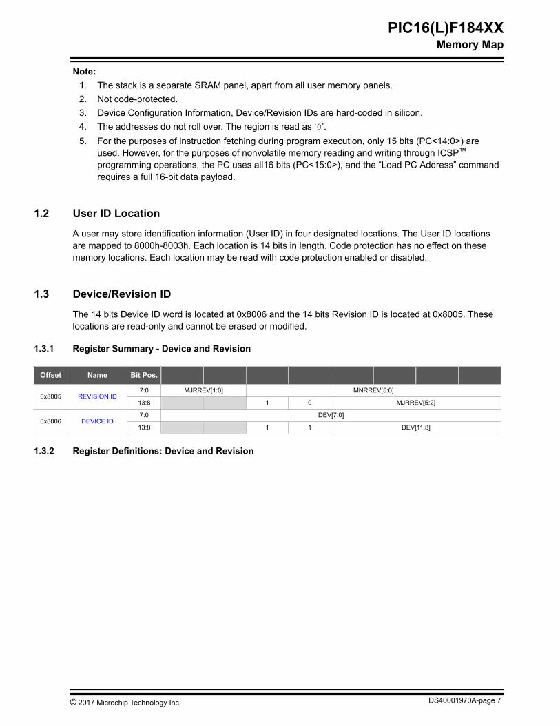
Related LinksDevice IDs and Checksums
PIC16(L)F184XXMemory Map
copy 2017 Microchip Technology Inc DS40001970A-page 9
1322 REVISION ID
Name REVISION IDOffset 0x8005
Revision ID Register
Bit 15 14 13 12 11 10 9 8 1 0 MJRREV[52]
Access R R R R R R Reset 1 0
Bit 7 6 5 4 3 2 1 0 MJRREV[10] MNRREV[50]
Access R R R R R R R R Reset
Bit 13 ndash 1 Read as lsquo1rsquoThese bits are fixed with value lsquo1rsquo for all devices in this family
Bit 12 ndash 0 Read as lsquo0rsquoThese bits are fixed with value lsquo0rsquo for all devices in this family
Bits 116 ndash MJRREV[50] Major Revision ID bitsThese bits are used to identify a major revision
Bits 50 ndash MNRREV[50] Minor Revision ID bitsThese bits are used to identify a minor revision
14 Configuration WordsThe devices have five Configuration Words starting at address 8007h through 800Bh The Configurationbits establish configuration values prior to the execution of any software Configuration bits enable ordisable device-specific features
In terms of programming these important Configuration bits should be considered1 LVP Low-Voltage Programming Enable Bit
ndash 1 = ON ndash Low-Voltage Programming is enabled MCLRVPP pin function is MCLR MCLREConfiguration bit is ignored
ndash 0 = OFF ndash HV on MCLRVPP must be used for programming2 CP User Nonvolatile Memory (NVM) Program Memory Code Protection bit
ndash 1 = OFF ndash User NVM code protection disabledndash 0 = ON ndash User NVM code protection enabled
Related LinksLow-Voltage Programming (LVP) ModeCode Protection
PIC16(L)F184XXMemory Map
copy 2017 Microchip Technology Inc DS40001970A-page 10
141 Register Summary - Configuration Words
Offset Name Bit Pos
0x8007 CONFIG170 RSTOSC[20] FEXTOSC[20]
138 FCMEN CSWEN CLKOUTEN
0x8008 CONFIG270 BOREN LPBOREN PWRTS[10] MCLRE
138 DEBUG STVREN PPS1WAY ZCDDIS BORV
0x8009 CONFIG370 WDTE[10] WDTCPS[40]
138 WDTCCS[20] WDTCWS[20]
0x800A CONFIG470 WRTAPP SAFEN BBEN BBSIZE[20]
138 LVP WRTSAF WRTD WRTC WRTB
0x800B CONFIG570 CP
138
142 Register Definitions Configuration Words
PIC16(L)F184XXMemory Map
copy 2017 Microchip Technology Inc DS40001970A-page 11
1421 CONFIG1
Name CONFIG1Offset 0x8007
Configuration word 1
Oscillators
Bit 15 14 13 12 11 10 9 8 FCMEN CSWEN CLKOUTEN
Access RP U RP U U RP Reset 1 1 1 1 1 1
Bit 7 6 5 4 3 2 1 0 RSTOSC[20] FEXTOSC[20]
Access U RP RP RP U RP RP RP Reset 1 1 1 1 1 1 1 1
Bit 13 ndash FCMEN Fail-Safe Clock Monitor Enable bit
Value Description1 FSCM timer enabled0 FSCM timer disabled
Bit 11 ndash CSWEN Clock Switch Enable bit
Value Description1 Writing to NOSC and NDIV is allowed0 The NOSC and NDIV bits cannot be changed by user software
Bit 8 ndash CLKOUTEN Clock Out Enable bit
Value Condition Description1 If FEXTOSC = EC (high mid or low) or Not
EnabledCLKOUT function is disabled IO or oscillatorfunction on OSC2
0 If FEXTOSC = EC (high mid or low) or NotEnabled
CLKOUT function is enabled FOSC4 clockappears at OSC2
Otherwise This bit is ignored
Bits 64 ndash RSTOSC[20] Power-up Default Value for COSC bitsThis value is the Reset default value for COSC and selects the oscillator first used by user softwareRefer to COSC operation
Value Description111 EXTOSC operating per FEXTOSC bits110 HFINTOSC (1 MHz) with OSCFRQ = lsquo010rsquo (4 MHz) and CDIV = lsquo0010rsquo (41)101 LFINTOSC100 SOSC011 Reserved010 EXTOSC with 4x PLL with EXTOSC operating per FEXTOSC bits
PIC16(L)F184XXMemory Map
copy 2017 Microchip Technology Inc DS40001970A-page 12
Value Description001 HFINTOSC with 2x PLL (32 MHz) with OSCFRQ = lsquo101rsquo (16 MHz) and CDIV = lsquo0000rsquo (11)000 Reserved
Bits 20 ndash FEXTOSC[20] FEXTOSC External Oscillator Mode Selection bits
Value Description111 ECH (External Clock) above 8 MHz110 ECM (External Clock) for 100 kHz to 8 MHz101 ECL (External Clock) below 100 kHz100 Oscillator not enabled011 Reserved (do not use)010 HS (Crystal oscillator) above 4 MHz001 XT (Crystal oscillator) above 100 kHz below 4 MHz000 LP (crystal oscillator) optimized for 32768 kHz
PIC16(L)F184XXMemory Map
copy 2017 Microchip Technology Inc DS40001970A-page 13
1422 CONFIG2
Name CONFIG2Offset 0x8008
Configuration Word 2
Supervisor
Bit 15 14 13 12 11 10 9 8 DEBUG STVREN PPS1WAY ZCDDIS BORV
Access RP RP RP RP RP U Reset 1 1 1 1 1 1
Bit 7 6 5 4 3 2 1 0 BOREN[10] LPBOREN PWRTS[10] MCLRE
Access RP RP RP U U RP RP RP Reset 1 1 1 1 1 1 1 1
Bit 13 ndash DEBUG Debugger Enable bit(1)
Value Description1 Background debugger disabled0 Background debugger enabled
Bit 12 ndash STVREN Stack OverflowUnderflow Reset Enable bit
Value Description1 Stack Overflow or Underflow will cause a Reset0 Stack Overflow or Underflow will not cause a Reset
Bit 11 ndash PPS1WAY PPSLOCKED bit One-Way Set Enable bit
Value Description1 The PPSLOCKED bit can be cleared and set only once PPS registers remain locked after
one clearset cycle0 The PPSLOCKED bit can be set and cleared repeatedly (subject to the unlock sequence)
Bit 10 ndash ZCDDIS ZCD Disable bit
Value Description1 ZCD disabled ZCD can be enabled by setting the ZCDSEN bit of the ZCDCON register0 ZCD always enabled ZCDSEN bit is ignored
Bit 9 ndash BORV Brown-out Reset Voltage Selection bit
Value Description1 Brown-out Reset voltage (VBOR) set to lower trip point level0 Brown-out Reset voltage (VBOR) set to higher trip point level
Bits 76 ndash BOREN[10] Brown-out Reset Enable bitsWhen enabled Brown-out Reset Voltage (VBOR) is set by BORV bit
PIC16(L)F184XXMemory Map
copy 2017 Microchip Technology Inc DS40001970A-page 14
Value Description11 Brown-out Reset enabled SBOREN bit is ignored10 Brown-out Reset enabled while running disabled in Sleep SBOREN is ignored01 Brown-out Reset enabled according to SBOREN00 Brown-out Reset disabled
Bit 5 ndash LPBOREN Low-Power BOR Enable bit
Value Description1 Low-Power Brown-out Reset is disabled0 Low-Power Brown-out Reset is enabled
Bits 21 ndash PWRTS[10] Power-up Timer Selection bits
Value Description11 PWRT disabled10 PWRT set at 64 ms01 PWRT set at 16 ms00 PWRT set at 1 ms
Bit 0 ndash MCLRE Master Clear (MCLR) Enable bit
Value Condition DescriptionIf LVP = 1 RE3 pin function is MCLR (it will reset the device when driven low)
1 If LVP = 0 MCLR pin is MCLR (it will reset the device when driven low)0 If LVP = 0 MCLR pin function is port defined function
Note 1 The DEBUG bit in Configuration Words is managed automatically by device development tools
including debuggers and programmers For normal device operation this bit should be maintainedas a lsquo1rsquo
PIC16(L)F184XXMemory Map
copy 2017 Microchip Technology Inc DS40001970A-page 15
1423 CONFIG3
Name CONFIG3Offset 0x8009
Configuration Word 3
Windowed Watchdog Timer
Bit 15 14 13 12 11 10 9 8 WDTCCS[20] WDTCWS[20]
Access RP RP RP RP RP RP Reset 1 1 1 1 1 1
Bit 7 6 5 4 3 2 1 0 WDTE[10] WDTCPS[40]
Access U RP RP RP RP RP RP RP Reset 1 1 1 1 1 1 1 1
Bits 1311 ndash WDTCCS[20] WDT Input Clock Selector bits
Value Description111 Software Control110 to011
Reserved
010 Reserved (no clock)32 kHz SOSC001 WDT reference clock is the 3125 kHz HFINTOSC (MFINTOSC) output000 WDT reference clock is the 310 kHz LFINTOSC
Bits 108 ndash WDTCWS[20] WDT Window Select bits
WDTCWS
WDTCON1 [WINDOW] at PORSoftwarecontrol ofWINDOW
Keyed accessrequiredValue
Window delayPercent of
time
Windowopening
Percent oftime
111 111 na 100 Yes No
110 110 na 100
No Yes
101 101 25 75
100 100 375 625
011 011 50 50
010 010 625 375
001 001 75 25
000 000 875 125
Bits 65 ndash WDTE[10] WDT Operating Mode bits
PIC16(L)F184XXMemory Map
copy 2017 Microchip Technology Inc DS40001970A-page 16
Value Description11 WDT enabled regardless of Sleep SEN is ignored10 WDT enabled while Sleep = 0 suspended when Sleep = 1 SEN bit is ignored01 WDT enableddisabled by SEN bit00 WDT disabled SEN bit is ignored
Bits 40 ndash WDTCPS[40] WDT Period Select bits
WDTCPSWDTCON0[WDTPS] at POR
Software Control of WDTPSValue Divider Ratio
Typical Time Out(FIN = 31 kHz)
11111 01011 165536 216 2s Yes
11110
10011
11110
10011132 25 1 ms No
10010 10010 18388608 223 256s
No
10001 10001 14194304 222 128s
10000 10000 12097152 221 64s
01111 01111 11048576 220 32s
01110 01110 1524299 219 16s
01101 01101 1262144 218 8s
01100 01100 1131072 217 4s
01011 01011 165536 216 2s
01010 01010 132768 215 1s
01001 01001 116384 214 512 ms
01000 01000 18192 213 256 ms
00111 00111 14096 212 128 ms
00110 00110 12048 211 64 ms
00101 00101 11024 210 32 ms
00100 00100 1512 29 16 ms
00011 00011 1256 28 8 ms
00010 00010 1128 27 4 ms
00001 00001 164 26 2 ms
00000 00000 132 25 1 ms
PIC16(L)F184XXMemory Map
copy 2017 Microchip Technology Inc DS40001970A-page 17
1424 CONFIG4
Name CONFIG4Offset 0x800A
Configuration Word 4
Memory Write Protection
Bit 15 14 13 12 11 10 9 8 LVP WRTSAF WRTD WRTC WRTB
Access RW U RW RW RW RW Reset 1 1 1 1 1 1
Bit 7 6 5 4 3 2 1 0 WRTAPP SAFEN BBEN BBSIZE[20]
Access RW U U RW RW RW RW RW Reset 1 1 1 1 1 0 0 1
Bit 13 ndash LVP Low-Voltage Programming Enable bitThe LVP bit cannot be written (to zero) while operating from the LVP programming interface The purposeof this rule is to prevent the user from dropping out of LVP mode while programming from LVP mode oraccidentally eliminating LVP mode from the Configuration state
The preconditioned (erased) state for this bit is critical
Value Description1 Low-voltage programming enabled MCLRVPP pin function is MCLR MCLRE Configuration
bit is ignored0 HV on MCLRVPP must be used for programming
Bit 11 ndash WRTSAF Storage Area Flash Write Protection bit(1)
Value Description1 SAF NOT write-protected0 SAF write-protected
Bit 10 ndash WRTD Data EEPROM Write Protection bit(1)
Value Description1 Data EEPROM NOT write-protected0 Data EEPROM write-protected
Bit 9 ndash WRTC Configuration Register Write Protection bit(1)
Value Description1 Configuration Registers NOT write-protected0 Configuration Registers write-protected
Bit 8 ndash WRTB Boot Block Write Protection bit(1)
PIC16(L)F184XXMemory Map
copy 2017 Microchip Technology Inc DS40001970A-page 18
Value Description1 Boot Block NOT write-protected0 Boot Block write-protected
Bit 7 ndash WRTAPP Application Block Write Protection bit(1)
Value Description1 Application Block NOT write-protected0 Application Block write-protected
Bit 4 ndash SAFEN SAF Enable bit(1)
Value Description1 SAF disabled0 SAF enabled
Bit 3 ndash BBEN Boot Block Enable bit(1)
Value Description1 Boot Block disabled0 Boot Block enabled
Bits 20 ndash BBSIZE[20] Boot Block Size Selection bitsBBSIZE is used only when BBEN = 0BBSIZE bits can only be written while BBEN = 1 after BBEN = 0 BBSIZ is write-protected
Table 1-1 Boot Block Size Bits
BBEN BBSIZEActual Boot Block Size User Program Memory
Size (words)Last Boot
Block MemoryAccess4k 8k 16k
1 xxx 0 0 0 mdash
0 111 512 512 512 01FFh
0 110 1024 1024 1024 03FFh
0 101
2048
2048 2048 07FFh
0 100
4096
4096 0FFFh
0 011
8192 1FFFh0 010
0 001
0 000
Note The maximum boot block size is half the user program memory size All selections higher thanthe maximum are set to half size For example all BBSIZE = 000 - 100 produce a boot block size of 4kW on a 8 kW device
Note
PIC16(L)F184XXMemory Map
copy 2017 Microchip Technology Inc DS40001970A-page 19
1 Bits are implemented as sticky bits Once protection is enabled it can only be reset through a BulkErase
PIC16(L)F184XXMemory Map
copy 2017 Microchip Technology Inc DS40001970A-page 20
1425 CONFIG5
Name CONFIG5Offset 0x800B
Configuration Word 5
Code Protection
Bit 15 14 13 12 11 10 9 8
Access U U U U U U Reset 1 1 1 1 1 1
Bit 7 6 5 4 3 2 1 0 CP
Access U U U U U U U RP Reset 1 1 1 1 1 1 1 1
Bit 0 ndash CP Program Flash Memory Code Protection bit
Value Description1 Program Flash Memory code protection disabled0 Program Flash Memory code protection enabled
15 Device Information AreaThe Device Information Area (DIA) is a dedicated region in the Program Flash Memory The data ismapped from 8100h to 811Fh These locations are read-only and cannot be erased or modified The DIAholds the calibration data for the temperature indicator module and the FVR voltages which are useful fortemperature sensing applications and calibration
Related LinksAppendix D Device Information Area (DIA)
16 Device Configuration InformationThe Device Configuration Information (DCI) is a dedicated region in the Program Flash Memory mappedfrom 8200h to 821Fh The data stored in the DCI memory is hard-coded into the device duringmanufacturing The DCI holds information about the device which is useful for programming andbootloaders These locations are read-only and cannot be erased or modified For more information referto the product-specific data sheet
Related LinksAppendix C Device Configuration Information (DCI)
PIC16(L)F184XXMemory Map
copy 2017 Microchip Technology Inc DS40001970A-page 21
2 Programming Algorithms
21 ProgramVerify ModeIn ProgramVerify mode the program memory and the configuration memory can be accessed andprogrammed in serial fashion ICSPDAT and ICSPCLK are used for the data and the clock respectivelyAll commands and data words are transmitted MSb first Data changes on the rising edge of theICSPCLK and is latched on the falling edge In ProgramVerify mode both the ICSPDAT and ICSPCLKare Schmitt Trigger inputs The sequence that enters the device into ProgramVerify mode places all otherlogic into the Reset state Upon entering ProgramVerify mode all IOs are automatically configured ashigh-impedance inputs On entering the ProgramVerify mode the address is cleared
211 High-Voltage ProgramVerify Mode Entry and Exit
There are two different methods of entering ProgramVerify mode via high voltagebull VPP ndash First Entry modebull VDD ndash First Entry mode
2111 VPP ndash First Entry Mode
To enter ProgramVerify mode via the VPP-First mode the following sequence must be followed1 Hold ICSPCLK and ICSPDAT low All other pins should be unpowered2 Raise the voltage on MCLR from 0V to VIHH3 Raise the voltage on VDD from 0V to the desired operating voltage
The VPP-first entry prevents the device from executing code prior to entering ProgramVerify mode Forexample when the Configuration Word has MCLR disabled (MCLRE = 0) the Power-up Timer isdisabled (PWRTS = 0) the internal oscillator is selected (FOSC = 100) and ICSPDAT and ICSPCLK aredriven by the user application the device will execute code and may drive the ICSPDAT and ISCPCLKIO pins Since code execution may prevent first entry VPP-First Entry mode is strongly recommended asit prevents user code from changing EEPROM contents or driving pins to affect Test mode entry
Related LinksProgramVerify Mode Exit
2112 VDD ndash First Entry ModeTo enter ProgramVerify mode via the VDD-First mode the following sequence must be followed
1 Hold ICSPCLK and ICSPDAT low2 Raise the voltage on VDD from 0V to the desired operating voltage3 Raise the voltage on MCLR from VDD or below to VIHH
The VDD-First mode is useful when programming the device when VDD is already applied for it is notnecessary to disconnect VDD to enter ProgramVerify mode During this cycle any executing code will beinterrupted and halted
Related LinksProgramVerify Mode Exit
PIC16(L)F184XXProgramming Algorithms
copy 2017 Microchip Technology Inc DS40001970A-page 22
2113 ProgramVerify Mode ExitTo exit ProgramVerify mode lower MCLR from VIHH to VIL VDD-First Entry mode should use VDD-LastExit mode (see Figure 2-1) VPP-First Entry mode should use VPP-Last Exit mode (see Figure 2-2)
Figure 2-1 Programming Entry and Exit Modes ndash VPP First and LastPROGRAMMING MODE ENTRY ndash EXIT
VPP LAST
TEXIT
PROGRAMMING MODE ENTRY ndash ENTRY VPP FIRST
TENTS TENTH
VDD
VIHH
VPP
ICSPDAT
ICSPCLK
VIL
Figure 2-2 Programming Entry and Exit Modes ndash VDD First and LastPROGRAMMING MODE ENTRY ndash ENTRY
VDD FIRST
PROGRAMMING MODE ENTRY ndash EXIT VDD LAST
TENTS TENTH
VDD
VIHH
VPP
ICSPDAT
ICSPCLK
VIL
TEXIT
212 Low-Voltage Programming (LVP) ModeThe Low-Voltage Programming mode allows the devices to be programmed using VDD only without highvoltage When the LVP bit of the Configuration Word 4 register is set to lsquo1rsquo the low-voltage ICSPprogramming entry is enabled To disable the Low-Voltage ICSP mode the LVP bit must be programmedto lsquo0rsquo This can only be done while in the High-Voltage Entry mode
Entry into the Low-Voltage ICSP ProgramVerify mode requires the following steps1 MCLR is brought to VIL
PIC16(L)F184XXProgramming Algorithms
copy 2017 Microchip Technology Inc DS40001970A-page 23
2 A 32-bit key sequence is presented on ICSPDAT The LSb of the pattern is a ldquodonrsquot care xrdquo TheProgramVerify mode entry pattern detect hardware verifies only the first 31 bits of the sequenceand the last clock is required to activate the ProgramVerify mode
The key sequence is a specific 32-bit pattern 32rsquoh4d434850 (more easily remembered as MCHP inASCII) The device will enter ProgramVerify mode only if the sequence is valid The Most Significant bitof the Most Significant nibble must be shifted in first Once the key sequence is complete MCLR must beheld at VIL for as long as ProgramVerify mode is to be maintained For low-voltage programming timingsee Figure 2-3 and Figure 2-4Figure 2-3 LVP Entry (Powering-Up)
TCKLTCKH
32 Clocks
31 30 29 1
TDHTDS
TENTH
MSb of Pattern LSb of Pattern
VDD
MCLR
ICSPDAT
TENTS
ICSPCLK
Figure 2-4 LVP Entry (Powered)
TCKH TCKL
32 Clocks
31 30 29 1
TDHTDS
TENTH
MSb of Pattern LSb of Pattern
VDD
MCLR
ICSPCLK
ICSPDAT
Exiting ProgramVerify mode is done by raising MCLR from below VIL to VIH level (or higher up to VDD)Note To enter LVP mode the MSb of the Most Significant nibble must be shifted in first This differsfrom entering the key sequence on some other device families
213 ProgramVerify Commands
Once a device has entered ICSP ProgramVerify mode (using either high voltage or LVP entry) theprogramming host device may issue commands to the microcontroller each eight bits in length Thecommands are summarized in the following table The commands are used to erase and program thedevice The commands load and use the Program Counter (PC)
Some of the 8-bit commands also have a data payload associated with it (such as Load Data for NVMand Read Data from NVM)
PIC16(L)F184XXProgramming Algorithms
copy 2017 Microchip Technology Inc DS40001970A-page 24
If the programming host device issues an 8-bit command byte that has a data payload associated with itthe host device is responsible for sending an additional 24 clock pulses (for example three 8-bit bytes) inorder to send or receive the payload data associated with the command
The actual payload bits associated with a command are command-specific and will be fewer than 24 bitsHowever the payload field is always padded with additional Start Stop and Pad bits to bring the totalpayload field size to 24 bits so as to be compatible with many 8-bit SPI-based systems
Within a 24-bit payload field the first bit transmitted is always a Start bit followed by a variable number ofPad bits followed by the useful data payload bits and ending with one Stop bit The useful data payloadbits are always transmitted Most Significant bit (MSb) first
When the programming device issues a command that involves a host to microcontroller payload (forexample Load PC Address) the Start Stop and Pad bits should all be driven by the programmer to lsquo0rsquoWhen the programming host device issues a command that involves microcontroller to host payload data(for example Read Data from NVM) the Start Stop and Pad bits should be treated as ldquodont carerdquo bitsand the values should be ignored by the host
When the programming host device issues an 8-bit command byte to the microcontroller the host shouldwait a minimum amount of delay (see the following table) prior to sending any additional clock pulses(associated with either a 24-bit data payload field or the next command byte)
Table 2-1 ICSPtrade Command Set Summary
CommandName
Command ValuePayload
ExpectedDelay afterCommand DataNoteBinary
(MSbLSb) Hex
Load PCAddress
1000 0000 80 Yes TDLYPC = payloadvalue
Bulk EraseProgramMemory
0001 1000 18 No TERAB
Depending onthe currentvalue of the PCone or morememoryregions
Row EraseProgramMemory
1111 0000 F0 No TERAR
The rowaddressed bythe MSbs of thePC is erasedLSbs areignored
Load Data forNVM
0000 00J0 0002 Yes TDLY
J = 1 PC = PC+ 1 after writingJ = 0 PC isunchanged
Read Data fromNVM
1111 11J0 FEFC Yes TDLY
J = 1 PC = PC+ 1 afterreading J = 0
PIC16(L)F184XXProgramming Algorithms
copy 2017 Microchip Technology Inc DS40001970A-page 25
CommandName
Command ValuePayload
ExpectedDelay afterCommand DataNoteBinary
(MSbLSb) Hex
PC isunchanged
IncrementAddress
1111 1000 F8 No TDLY PC = PC + 1
Begin InternallyTimedProgramming
1110 0000 E0 No TPINT
Commitslatched data toNVM (selftimed)
BeginExternallyTimedProgramming
1100 0000 C0 No TPEXT
Commitslatched data toNVM (externallytimed) AfterTPEXT ldquoEndExternallyTimedProgrammingrdquocommand mustbe issued
End ExternallyTimedProgramming
1000 0010 82 No TDIS
Should beissued withinrequired timedelay (TPEXT)after ldquoBeginExternallyTimedProgrammingrdquocommand
Note All clock pulses for both the 8-bit commands and the 24-bit payload fields are generated by thehost programming device The microcontroller does not drive the ICSPCLK line The ICSPDAT signal is abidirectional data line For all commands and payload fields except the Read Data from NVM payloadthe host programming device continuously drives the ICSPDAT line Both the host programmer deviceand the microcontroller should latch received ICSPDAT values on the falling edge of the ICSPCLK lineISCPDAT timing will be met as per Figure 2-5
PIC16(L)F184XXProgramming Algorithms
copy 2017 Microchip Technology Inc DS40001970A-page 26
Figure 2-5 Clock and Data Timing
as
ICSPCLK
TCKH TCKL
TDHTDS
ICSPDAT
Output
TCOICSPDAT
ICSPDAT
ICSPDAT
TLZD
THZD
Input
as
from Input
from Output to Input
to Output
2131 Load Data for NVM
The Load Data for NVM command is used to load one programming data latch (for example one 14-bitinstruction word for program memoryconfiguration memoryUser ID memory or one 8-bit byte for anEEPROM data memory address) The Load Data for NVM command can be used to load data forProgram Flash Memory (see Figure 2-6) or the EEPROM if available (see Figure 2-7) The word writesinto program memory after the Begin Internally Timed Programming or Begin Externally TimedProgramming commands write the entire row of data latches not just one word The lower five bits of theaddress are considered while the other bits are ignored Depending on the value of bit 1 of thecommand the Program Counter (PC) may or may not be incremented (see Table 2-1)
Figure 2-6 Load Data for NVM (Program Flash Memory)
ICSPCLK
ICSPDAT
7 6 5 4 3 2 23 22 1 0
00 0 MSb0 0 0
TDLY
1 0 1415
0 J 0 00 LSb
Stop BitStart Bit
8-Bit Command 24-Bit Payload Field
0
TDLY
Figure 2-7 Load Data for NVM (EEPROM)
ICSPCLK
ICSPDAT
7 6 5 4 3 2 23 22 1 0
00 0 MSb0 0 0
TDLY
1 0 89
0 J 0 00 LSb
Stop BitStart Bit
8-Bit Command 24-Bit Payload Field
0
TDLY
PIC16(L)F184XXProgramming Algorithms
copy 2017 Microchip Technology Inc DS40001970A-page 27
Related LinksRow Erase Memory
2132 Read Data from NVMThe Read Data from NVM command will transmit data bits out of the current PC address The ICSPDATpin will go into Output mode on the first falling edge of ICSPCLK and it will revert to Input mode (high-impedance) after the 24th falling edge of the clock The Start and Stop bits are only one half of a bit timewide and should therefore be ignored by the host programmer device (since the latched value may beindeterminate) Additionally the host programmer device should only consider the MSb to LSb payloadbits as valid and should ignore the values of the pad bits If the program memory is code-protected (CP =0) the data will be read as zeros (see Figure 2-8 and Figure 2-9) Depending on the value of bit lsquo1rsquo of thecommand the PC may or may not be incremented (see Table 2-1) The Read Data for NVM commandcan be used to read data for Program Flash Memory (see Figure 2-8) or the EEPROM (see Figure 2-9)
Figure 2-8 Read Data from NVM (Program Flash Memory or Configuration Words)
ICSPCLK
ICSPDAT
7 6 5 4 3 2 23 22 1 0
1 1 0
MSb
1 1 1
TDLY
1 0 1415
1 J
LSb
StopStart
(from Programmer)
ICSPDAT (from device)
Data
High-Z
0 0
Input
High-Z
Input Output
TDLY
x x
Figure 2-9 Read Data from NVM (EEPROM)
ICSPCLK
ICSPDAT
23 22 1 0
11 0
MSb
1 1 1
TDLY
89
1 J
LSb
StopStart
(from Programmer)
ICSPDAT (from device)
Data
High-Z
0 0High-Z
7 6 5 4 3 2 1 0
Input Input Output
TDLY
x x
2133 Load PC Address
The PC value is set using the supplied data The address implies the memory panel (Program FlashMemory or EEPROM) to be accessed (see the figure below)
PIC16(L)F184XXProgramming Algorithms
copy 2017 Microchip Technology Inc DS40001970A-page 28
Figure 2-10 Load PC Address
ICSPCLK
ICSPDAT0 0 0 MSb1 0 0
TDLY
0 0 0 0 0 LSb
Stop Start
Address 0
23 22 1 0 16 17 7 6 5 4 3 2 1 0
TDLY
2134 Increment AddressThe PC is incremented by one when this command is received It is not possible to decrement theaddress To reset this counter the user must use the Load PC Address command This commandperforms the same action as the J bit in the LoadRead commands See the figure below
Figure 2-11 Increment Address
ICSPCLK
ICSPDAT
7 6 5 4 3 2 7 6
0 1 0 1 1 1
1 0
1 0
TDLY
5Next Command
X X X
Address + 1Address
2135 Begin Internally Timed Programming
The write programming latches must already have been loaded using the Load Data for NVM commandprior to issuing the Begin Programming command Programming of the addressed memory row will beginafter this command is received The lower LSBs of the address are ignored An internal timingmechanism executes the write The user must allow for the EraseWrite cycle time TPINT in order for theprogramming to complete prior to issuing the next command (see the figure below)
After the programming cycle is complete all the data latches are reset to lsquo1rsquoFigure 2-12 Begin Internally Timed Programming
ICSPCLK
ICSPDAT
7 6 5 4 3 2 7 6
0 0 0 1 1 0
1 0
1 0
5Next Command
X X X
TPINT
2136 Begin Externally Timed Programming
Data to be programmed must be previously loaded by Load Data for NVM command before every BeginProgramming command To complete the programming the End Externally Timed Programmingcommand must be sent in the specified time window defined by TPEXT (see the figure below) The lowerLSBs of the address are ignored
Externally timed writes are not supported for Configuration bits Any externally timed write to theConfiguration Word will have no effect on the targeted word
PIC16(L)F184XXProgramming Algorithms
copy 2017 Microchip Technology Inc DS40001970A-page 29
Figure 2-13 Begin Externally Timed Programming
ICSPCLK
ICSPDAT
7 6 5 4 3 2 7 6
0 0 0 1 0 0
1 0
1 0
5
End Externally Timed Programming
1 0 0
TPEXT
Command
2137 End Externally Timed Programming
This command is required to terminate the programming sequence after a Begin Externally TimedProgramming command is given If no programming command is in progress or if the programming cycleis internally timed this command will execute as a No Operation (NOP) (see the figure below)
Figure 2-14 End Program Timing
ICSPCLK
ICSPDAT
7 6 5 4 3 2 7 6
00 0 1 0 0
1 0
0 1
5
X X X
TDIS
Next Command
2138 Bulk Erase Memory
The Bulk Erase Memory command performs different functions dependent on the current PC addressThe Bulk Erase command affects specific portions of the memory depending on the initial value of theProgram Counter Whenever a Bulk Erase command is executed the device will erase all bytes within theregions listed in Table 2-2 While a programming command is in progress this command executes as aNOP
After receiving the Bulk Erase Memory command the erase will not complete until the time intervalTERAB has expired (see Figure 2-15) The programming host device should not issue another 8-bitcommand until after the TERAB interval has fully elapsedTable 2-2 Bulk Erase Table
AddressArea(s) Erased
CP=1 CP=0
0000h-7FFFhUser Flash User FlashConfiguration Words Configuration Words
8000h-80FDhUser Flash User FlashConfiguration Words Configuration WordsUser ID words User ID words
80FEh-80FFh User Flash User Flash8100h-E7FFh No Operation No Operation
E800h-FFFFhUser Flash User FlashConfiguration Words Configuration WordsUser ID words User ID words
PIC16(L)F184XXProgramming Algorithms
copy 2017 Microchip Technology Inc DS40001970A-page 30
Figure 2-15 Bulk Erase Memory
ICSPCLK
ICSPDAT
7 6 5 4 3 2 7 6
0 1 0 0 0 1
1 0
0 0
5Next Command
X X X
TERAB
2139 Row Erase Memory
If the program memory is code-protected the Row Erase Program Memory command will be ignoredWhen the address is 8000h-8004h the Row Erase Program Memory command will only erase the UserID locations regardless of the setting of the CP Configuration bit The Row Erase Memory command willerase an individual row When write and erase operations are done on a row basis the row size (numberof 14-bit words) for erase operation is 32 and the row size (number of 14-bit latches) for the writeoperation is 32
The Flash memory row defined by the current PC will be erased The user must wait TERAR for erasing tocomplete (see the figure below)
Figure 2-16 Row Erase Memory
ICSPCLK
ICSPDAT
7 6 5 4 3 2 7 6
0 0 0 1 1 1
1 0
1 0
5Next Command
X X X
TERAR
22 Programming Algorithms
The device uses internal latches to temporarily store the 14-bit words used for programming The datalatches allow the user to program a full row with a single Begin Internally Timed Programming or BeginExternally Timed Programming command The Load Data for NVM command is used to load a singledata latch The data latch will hold the data until the Begin Internally Timed Programming or BeginExternally Timed Programming command is given
The data latches are aligned with the LSbs of the address The address at the time the Begin InternallyTimed Programming or Begin Externally Timed Programming command is given will determine whichmemory row is written Writes cannot cross a physical row boundary For example attempting to writefrom address 0002h-0021h in a 32-latch device will result in data being written to 0020h-003Fh
If more than the maximum number of latches are written without a Begin Internally Timed Programming orBegin Externally Timed Programming command the data in the data latches will be overwritten Thefollowing flowcharts show the recommended flowcharts for programming
Note The Program Flash Memory region is programmed one row (32 words) at a time (Figure 2-20)while the Configuration words are programmed one word at a time (Figure 2-19) The EEPROM region isprogrammed one byte at a time The value of the PC at the time of issuing the Begin Internally TimedProgramming or Begin Externally Timed Programming command determines what row (of Program FlashMemory) what word (of Configuration Word) or what byte (EEPROM) will get programmed
PIC16(L)F184XXProgramming Algorithms
copy 2017 Microchip Technology Inc DS40001970A-page 31
Figure 2-17 Device ProgramVerify Flowchart
Done
Start
Bulk Erase Device
Write User IDs
Enter Programming Mode
Write Program Memory(1)
Verify User IDs
Write Configuration Words(2)
Verify Configuration Words
Exit Programming Mode
Write EEPROM
Verify EEPROM Memory
Verify Program Memory
Note 1 See Figure 2-102 See Figure 2-16
PIC16(L)F184XXProgramming Algorithms
copy 2017 Microchip Technology Inc DS40001970A-page 32
Figure 2-18 Program Memory Flowchart
Start
Read Data
NVM
Data Correct
ReportProgramming
Failure
All LocationsDone
No
NoIncrementPC Addressto Next Row
from
Bulk Erase
Program
Yes
Memory(1 2)
Done
Yes
Program Cycle(3)
Note 1 This step is optional if the device has already been erased or has not been previously programmed2 If the device is code-protected or must be completely erased then Bulk Erase the device per Figure
3-173 See Figure 2-15
PIC16(L)F184XXProgramming Algorithms
copy 2017 Microchip Technology Inc DS40001970A-page 33
Figure 2-19 One-Word Program Cycle
Begin Programming
Load Data for
NVM Command
Command (Internally Timed)
Wait TPINT
Program Cyle(for Programming Configuration Words)
PIC16(L)F184XXProgramming Algorithms
copy 2017 Microchip Technology Inc DS40001970A-page 34
Figure 2-20 Multiple-Word Program Cycle
Begin Programming
Wait TPINT
Load Data for NVM
Command (Internally timed)
Load Data for NVM
Increment Address
Load Data for NVM
Latch 1
Latch 2
Latch 32
Increment Address
Program Cycle (for Writing to Program Flash Memory)
Begin Programming
Wait TPEXT
Command (Externally timed)
End Externally Timed Programming
Wait TDIS
Command
PIC16(L)F184XXProgramming Algorithms
copy 2017 Microchip Technology Inc DS40001970A-page 35
Figure 2-21 Configuration Memory Program Flowchart
Start
Load PC Address
Program Cycle(2)
Read fromNVM Command
Data CorrectReport
ProgrammingFailure
Address =8004h
Data CorrectReport
ProgrammingFailure
No
Yes
Yes
No
IncrementPC
Address
No Load PCAddress
Command (8007h)
Done
One-word
One-wordProgram Cycle(2)
(Config Word)
(User ID)
Read Data
Commandfrom NVM
ProgramBulk Erase
Memory(1)
Yes
IncrementPC
Address
Address =800Ch
No
regions)(selects Bulk Erase
Load PC Address(8000h)
Note 1 This step is optional if the device is erased or not previously programmed2 See Figure 2-12
PIC16(L)F184XXProgramming Algorithms
copy 2017 Microchip Technology Inc DS40001970A-page 36
Figure 2-22 Bulk Erase Flowchart
Start
Load PC Address
Done
Bulk Erase Program Memory
(determines region(s) that will get erased)
Wait TERAB for Operation to Complete
23 Code Protection
Code protection is controlled using the CP bit When code protection is enabled all program memorylocations (0000h-7FFFh) read as lsquo0rsquo Further programming is disabled for the program memory(0000h-7FFFh) until the next Bulk Erase operation is performed Program memory can still beprogrammed and read during program execution
The Revision ID Device ID Device Information Area Device Configuration Information User IDs andConfiguration Words can be read out regardless of the code protection settings
231 Program Memory
Code protection is enabled by programming the CP bit to lsquo0rsquo The only way to disable code protection is touse the Bulk Erase Memory command (with the PC set to an address so as to Bulk Erase all programFlash contents)
24 Hex File UsageIn the hex file there are two bytes per program word stored in the Intelreg INHX32 hex format Data isstored LSB first MSB second Because there are two bytes per word the addresses in the hex file are 2xthe address in program memory For example if the Configuration Word 1 is stored at 8007h in the hexfile this will be referenced as 1000Eh-1000Fh
241 Configuration Word
To allow portability of code it is strongly recommended that the programmer is able to read theConfiguration Words and User ID locations from the hex file If the Configuration Words information wasnot present in the hex file a simple warning message may be issued Similarly while saving a hex fileConfiguration Words and User ID information should be included
PIC16(L)F184XXProgramming Algorithms
copy 2017 Microchip Technology Inc DS40001970A-page 37
242 Device ID
If a Device ID is present in the hex file at 1000Ch-1000Dh (8006h on the part) the programmer shouldverify the Device ID against the value read from the part On a mismatch condition the programmershould generate a warning message
243 Checksum Computation
The checksum is calculated by two different methods dependent on the setting of the CP Configurationbit
2431 Program Code Protection Disabled
With the program code protection disabled the checksum is computed by reading the contents of theprogram memory locations and summing up the program memory data starting at address 0000h up tothe maximum user addressable location (eg 0FFFh) Any Carry bits exceeding 16 bits are ignoredAdditionally the relevant bits of the Configuration Words are added to the checksum For PIC16 devices(14-bit program memory word) the two MSBs are taken as zero All unimplemented Configuration bitsare masked to lsquo0rsquo
Related LinksDevice IDs and Checksums
2432 Program Code Protection EnabledWhen the MPLABXreg IDE check box for Project Properties - Building - Insert unprotected checksum inUser ID memory is checked then the 16-bit checksum of the equivalent unprotected device is computedand stored in the User ID Each nibble of the unprotected checksum is stored in the Least Significantnibble of each of the four User ID locations The Most Significant checksum nibble is stored in the User IDat location 8000h the second Most Significant nibble is stored at location 8001h and so forth for theremaining nibbles and ID locations
The checksum of a code-protected device is computed in the following manner the Least Significantnibble of each User ID is used to create a 16-bit value The Least Significant nibble of User ID location8000h is the Most Significant nibble of the 16-bit value The Least Significant nibble of User ID location8001h is the second Most Significant nibble and so forth for the remaining User IDs and 16-bit valuenibbles The resulting 16-bit value is summed with the Configuration Words All unimplementedConfiguration bits are masked to lsquo0rsquo
25 Electrical SpecificationsRefer to device-specific data sheet for absolute maximum ratings
Table 2-3 ACDC Characteristics Timing Requirements for ProgramVerify Mode
ACDC CHARACTERISTICS Standard Operating Conditions Production tested at 25degC
Sym Characteristics Min Typ Max Units ConditionsComments
Programming Supply Voltages and Currents
VDD
Supply Voltage(VDDMIN
(1)VDDMAX)
PIC16LF184XX 180 mdash 360 V
PIC16F184XX 230 mdash 550 V
VPEW ReadWrite and Row Erase operations VDDMIN mdash VDDMAX V
PIC16(L)F184XXProgramming Algorithms
copy 2017 Microchip Technology Inc DS40001970A-page 38
ACDC CHARACTERISTICS Standard Operating Conditions Production tested at 25degC
Sym Characteristics Min Typ Max Units ConditionsComments
VBE Bulk Erase operations VBORMAX(2) mdash VDDMAX V
IDDI Current on VDD Idle mdash mdash 10 mAIDDP Current on VDD Programming mdash mdash 50 mA
IPPVPP
Current on MCLRVPP mdash mdash 600 microA
VIHHHigh Voltage on MCLRVPP forProgramVerify Mode Entry 79 mdash 90 V
TVHHRMCLR Rise Time (VIL to VIHH) forProgramVerify Mode Entry mdash mdash 10 micros
IO pins
VIH(ICSPCLK ICSPDAT MCLRVPP) InputHigh Level 08 VDD mdash mdash V
VIL(ICSPCLK ICSPDAT MCLRVPP) InputLow Level mdash mdash 02 VDD V
VOH ICSPDAT Output High LevelVDD-07VDD-07VDD-07
mdash mdash V
IOH = -35 mA VDD =5V IOH = -3 mA VDD= 33V IOH = -1 mA
VDD = 18V
VOL ICSPDAT Output Low Level mdash mdashVSS+06VSS+06VSS+06
V
IOL = 8 mA VDD =5V IOL = 6 mA VDD= 33V IOL = 18 mA
VDD = 18VProgramming Mode Entry and Exit
TENTS
Programing Mode Entry Setup TimeICSPCLK ICSPDAT Setup TimeBefore VDD or MCLRuarr
100 mdash mdash ns
TENTH
Programing Mode Entry Hold TimeICSPCLK ICSPDAT Hold Time afterVDD or MCLRuarr
250 mdash mdash micros
Serial ProgramVerifyTCKL Clock Low Pulse Width 100 mdash mdash nsTCKH Clock High Pulse Width 100 mdash mdash nsTDS Data in SETUP TIME before Clockdarr 100 mdash mdash nsTDH Data in HOLD TIME after Clockdarr 100 mdash mdash ns
TCOClockuarr to DATA OUT VALID (during aRead Data Command) 0 mdash 80 ns
TLZDClockdarr to Data Low-impedance (duringa Read Data Command) 0 mdash 80 ns
THZDClockdarr to Data High-impedance (duringa Read Data command) 0 mdash 80 ns
PIC16(L)F184XXProgramming Algorithms
copy 2017 Microchip Technology Inc DS40001970A-page 39
ACDC CHARACTERISTICS Standard Operating Conditions Production tested at 25degC
Sym Characteristics Min Typ Max Units ConditionsComments
TDLY
Data Input not Driven To Next ClockInput (delay required betweencommanddata or commandcommand)
10 mdash mdash micros
TERAB Bulk Erase Cycle Time mdash mdash 84 ms PIC16(L)F184XXdevices
TERAR Row Erase Cycle Time mdash mdash 28 ms
TPINTInternally Timed ProgrammingOperation Time
mdash mdash 28 ms Program memoryConfiguration Wordsmdash mdash 56 ms
TPEXT
Delay Required between BeginExternally Timed Programming andEnd Externally Timed ProgrammingCommands
10 mdash 21 ms (Note 3)
TDISDelay Required after End ExternallyTimed Programming Command 300 mdash mdash micros
TEXITTime Delay when Exiting ProgramVerify Mode 1 mdash mdash micros
Note 1 In case of Bulk Erase the devices default to brown-out enabled with BORV = 1 (low trip point) In order to
ensure that the device is not held in Brown-out Reset VDDMIN becomes the VBOR threshold (with BORV = 1)when performing low-voltage programming on a Bulk Erased device
2 Bulk Erase operation overrides the BOR setting and the minimum VBE threshold is the same for F and LFdevices Refer to the microcontroller data sheet specification for the exact value of VBORMAX
3 Externally timed writes are not supported for Configuration bits
PIC16(L)F184XXProgramming Algorithms
copy 2017 Microchip Technology Inc DS40001970A-page 40
3 Appendix A Revision History (122017)Initial release of this document
PIC16(L)F184XXAppendix A Revision History (122017)
copy 2017 Microchip Technology Inc DS40001970A-page 41
4 Appendix B Device ID Checksums and Pinout Descriptions
41 Device IDs and Checksums
Device DeviceID
Config 1 Config 2 Config 3 Config 4 Config 5 ChecksumW
ord
(HEX
)
Mas
k (H
EX)
Wor
d (H
EX)
Mas
k (H
EX)
Wor
d (H
EX)
Mas
k (H
EX)
Wor
d (H
EX)
Mas
k (H
EX)
Wor
d (u
npro
tect
ed)
Wor
d (p
rote
cted
)
Mas
k
Unprotected Code-protected
Blank(HEX)
00AAhFirstandLast
(HEX)
Blank(HEX)
00AAhFirstandLast
(HEX)
PIC16F18424 30CA 3FFF 2977 3FFF 3EE7 3FFF 3F7F 3FFF 2F9F 3FFF 3FFE 0001 C77D 48D3 9EF9 204FPIC16LF18424 30CB 3FFF 2977 3FFF 3EE7 3FFF 3F7F 3FFF 2F9F 3FFF 3FFE 0001 C77D 48D3 9EF9 204FPIC16F18425 30CC 3FFF 2977 3FFF 3EE7 3FFF 3F7F 3FFF 2F9F 3FFF 3FFE 0001 B77D 38D3 8EF9 104FPIC16LF18425 30CD 3FFF 2977 3FFF 3EE7 3FFF 3F7F 3FFF 2F9F 3FFF 3FFE 0001 B77D 38D3 8EF9 104FPIC16F18426 30D2 3FFF 2977 3FFF 3EE7 3FFF 3F7F 3FFF 2F9F 3FFF 3FFE 0001 977D 18D3 6EF9 F04FPIC16LF18426 30D3 3FFF 2977 3FFF 3EE7 3FFF 3F7F 3FFF 2F9F 3FFF 3FFE 0001 977D 18D3 6EF9 F04FPIC16F18444 30CE 3FFF 2977 3FFF 3EE7 3FFF 3F7F 3FFF 2F9F 3FFF 3FFE 0001 C77D 48D3 9EF9 204FPIC16LF18444 30CF 3FFF 2977 3FFF 3EE7 3FFF 3F7F 3FFF 2F9F 3FFF 3FFE 0001 C77D 48D3 9EF9 204FPIC16F18445 30D0 3FFF 2977 3FFF 3EE7 3FFF 3F7F 3FFF 2F9F 3FFF 3FFE 0001 B77D 38D3 8EF9 104FPIC16LF18445 30D1 3FFF 2977 3FFF 3EE7 3FFF 3F7F 3FFF 2F9F 3FFF 3FFE 0001 B77D 38D3 8EF9 104FPIC16F18446 30D4 3FFF 2977 3FFF 3EE7 3FFF 3F7F 3FFF 2F9F 3FFF 3FFE 0001 977D 18D3 6EF9 F04FPIC16LF18446 30D5 3FFF 2977 3FFF 3EE7 3FFF 3F7F 3FFF 2F9F 3FFF 3FFE 0001 977D 18D3 6EF9 F04FPIC16F18455 30D7 3FFF 2977 3FFF 3EE7 3FFF 3F7F 3FFF 2F9F 3FFF 3FFE 0001 B77D 38D3 8EF9 104FPIC16LF18455 30D8 3FFF 2977 3FFF 3EE7 3FFF 3F7F 3FFF 2F9F 3FFF 3FFE 0001 B77D 38D3 8EF9 104FPIC16F18456 30D9 3FFF 2977 3FFF 3EE7 3FFF 3F7F 3FFF 2F9F 3FFF 3FFE 0001 977D 18D3 6EF9 F04FPIC16LF18456 30DA 3FFF 2977 3FFF 3EE7 3FFF 3F7F 3FFF 2F9F 3FFF 3FFE 0001 977D 18D3 6EF9 F04F
42 Example Checksum Computed with Program Code Protection Disabled BlankDevice
Device Sum of Memory addresses0000h-0FFFh
F000h (1000h3FFFh)
PIC16F18424
Configuration Word 1 3FFFh
Configuration Word 1 mask 2977h
Configuration Word 2 3FFFh
Configuration Word 2 mask 3EE7h
Configuration Word 3 3FFFh
Configuration Word 3 mask 3F7Fh
Configuration Word 4 3FFFh
PIC16(L)F184XXAppendix B Device ID Checksums and Pinou
copy 2017 Microchip Technology Inc DS40001970A-page 42
Device Sum of Memory addresses0000h-0FFFh
F000h (1000h3FFFh)
Configuration Word 4 mask 2F9Fh
Configuration Word 5 Unprotected 3FFFh
Configuration Word 5 mask 0001h
Checksum = F000h + (3FFFh and 2977h) + (3FFFh and3EE7h) + (3FFFh and 3F7Fh) + (3FFFh and2F9Fh) + (3FFFh and 0001h)
= F000h + 2977h + 3EE7h + 3F7Fh + 2F9Fh+ 0001h
= C77Dh
43 Example Checksum Computed with Program Code Protection Disabled 00AAhat First and Last Address
Device Sum of Memory addresses0000h-0FFFh
7156h (AAh + (FFEh3FFFh) + AAh)
PIC16F18424
Configuration Word 1 3FFFh
Configuration Word 1 mask 2977h
Configuration Word 2 3FFFh
Configuration Word 2 mask 3EE7h
Configuration Word 3 3FFFh
Configuration Word 3 mask 3F7Fh
Configuration Word 4 3FFFh
Configuration Word 4 mask 2F9Fh
Configuration Word 5 Unprotected 3FFFh
Configuration Word 5 mask 0001h
Checksum = 7156h + (3FFFh and 2977h) + (3FFFh and3EE7h) + (3FFFh and 3F7Fh) + (3FFFh and2F9Fh) + (3FFFh and 0001h)
= 7156h + 2977h + 3EE7h + 3F7Fh + 2F9Fh+ 0001h
= 48D3h
PIC16(L)F184XXAppendix B Device ID Checksums and Pinou
copy 2017 Microchip Technology Inc DS40001970A-page 43
44 Example Checksum Computed with Program Code Protection Enabled BlankDeviceDevice
PIC16F18424
Configuration Word 1 3FFFh
Configuration Word 1 mask 2977h
Configuration Word 2 3FFFh
Configuration Word 2 mask 3EE7h
Configuration Word 3 3FFFh
Configuration Word 3 mask 3F7Fh
Configuration Word 4 3FFFh
Configuration Word 4 mask 2F9Fh
Configuration Word 5 Unprotected 3FFFh
Configuration Word 5 mask 0001h
Sum of User IDs = (000Ch and 000Fh) ltlt 12 + (0007h and 000Fh) ltlt8 + (0007h and 000Fh) ltlt 4 + (000Dh and 000Fh)
= C000h + 0700h + 0070h + 000Dh
= C77Dh
Checksum = (3FFFh and 2977h) + (3FFFh and 3EE7h)+ (3FFFh and 3F7Fh) + (3FFFh and 2F9Fh)+ (3FFEh and 0001h) + C77Dh
= 2977h + 3EE7h + 3F7Fh + 2F9Fh + 0000h +C77Dh
= 9EF9h
Related LinksProgram Code Protection Enabled
45 Example Checksum Computed with Program Code Protection Enabled 00AAh atFirst and Last AddressDevice
PIC16F18424
Configuration Word 1 3FFFh
Configuration Word 1 mask 2977h
Configuration Word 2 3FFFh
Configuration Word 2 mask 3EE7h
Configuration Word 3 3FFFh
PIC16(L)F184XXAppendix B Device ID Checksums and Pinou
copy 2017 Microchip Technology Inc DS40001970A-page 44
Device
Configuration Word 3 mask 3F7Fh
Configuration Word 4 3FFFh
Configuration Word 4 mask 2F9Fh
Configuration Word 5 Unprotected 3FFFh
Configuration Word 5 mask 0001h
Sum of User IDs (0004h and 000Fh) ltlt 12 + (0008h and 000Fh) ltlt 8+ (000Dh and 000Fh) ltlt 4 + (0003h and 000Fh)
= 4000h + 0800h + 00D0h + 0003h
= 48D3h
Checksum = (3FFFh and 2977h) + (3FFFh and 3EE7h)+ (3FFFh and 3F7Fh) + (3FFFh and 2F9Fh)+ (3FFEh and 0001h) + 48D3h
= 2977h + 3EE7h + 3F7Fh + 2F9Fh + 0000h+ 48D3h
= 204Fh
Related LinksProgram Code Protection Enabled
46 Programming Pin Locations by Package Type
Device PackageType
PkgCode
PackageDrawing
Number(1)VDDPIN
VSSPIN
MCLR ICSPCLK ICSPDAT
PIN PORT PIN PORT PIN PORT
PIC16(L)F18424PIC16(L)F18425PIC16(L)F18426
14 - PDIP (P) C04-005 1 14 4 RA3 12 RA1 13 RA014 - SOIC(39mm) (SL) C04-065 1 14 4 RA3 12 RA1 13 RA0
14 - TSSOP (ST) C04-087 1 14 4 RA3 12 RA1 13 RA016 - uQFN(4x4) (JQ) C04-257 16 13 3 RA3 11 RA1 12 RA0
PIC16(L)F18444PIC16(L)F18445PIC16(L)F18446
20 - PDIP (P) C04-019 1 20 4 RA3 18 RA1 19 RA020 - SOIC (SO) C04-094 1 20 4 RA3 18 RA1 19 RA020 - SSOP (SS) C04-072 1 20 4 RA3 18 RA1 19 RA020 - uQFN(4x4) (GZ) C04-255 18 17 1 RA3 15 RA1 16 RA0
PIC16(L)F18455PIC16(L)F18456
28 - SPDIP (SP) C04-070 20 19 1 RE3 27 RB6 28 RB728 - SSOP (SS) C04-073 20 19 1 RE3 27 RB6 28 RB728 - SOIC (SO) C04-052 20 19 1 RE3 27 RB6 28 RB728 - uQFN(4x4) (MV) C04-152 17 16 26 RE3 24 RB6 25 RB7
Note
PIC16(L)F184XXAppendix B Device ID Checksums and Pinou
copy 2017 Microchip Technology Inc DS40001970A-page 45
Device PackageType
PkgCode
PackageDrawing
Number(1)VDDPIN
VSSPIN
MCLR ICSPCLK ICSPDAT
PIN PORT PIN PORT PIN PORT
1 The most current package drawings can be found in the Microchip Packaging Specification DS00049 found at httpwwwmicrochipcompackaging The drawing numbers listed above do not include the current revision designator whichis added at the end of the number
PIC16(L)F184XXAppendix B Device ID Checksums and Pinou
copy 2017 Microchip Technology Inc DS40001970A-page 46
5 Appendix C Device Configuration Information (DCI)Table 5-1 Device Configuration Information
Address Description Value Units
8200h Erase Row Size 32 Words
8201h Number of WriteLatches
32 mdash
8202h Number of User Rows See Table 5-2 Rows
8203h EE Data Memory Size 256 Bytes
8204h Pin Count See Table 5-3 Pins
Table 5-2 Number of User Rows
Part Name Memory Size Number of User Rows
PIC16(L)F1842418444 4k 128
PIC16(L)F184251844518455 8k 256
PIC16(L)F184261844618456 16k 512
Table 5-3 Pin Count
Part Number Pin Count
PIC16(L)F184242526 14(1)
PIC16(L)F184444546 20
PIC16(L)F1845518456 28
Note 1 16 pin-count devices will show lsquo14rsquo in location 8204h
PIC16(L)F184XXAppendix C Device Configuration Informati
copy 2017 Microchip Technology Inc DS40001970A-page 47
6 Appendix D Device Information Area (DIA)Table 6-1 Device Information Area Address Locations and Descriptions
Address Range Standard Device Information Description8100h 8108h Microchip Unique Identifier (MUI) Unique indentifier based on silicon die information
8109h Reserved Reserved810Ah 8111h External Unique Indentifier (EUI) Optional area for placing customer-specific data
8112h Unassigned Unassigned
8113h Temp Sensor (Low-Range setting) 90degC
ADC conversion data of the Temperature Sensor(Low-Range setting) at 90degC setpoint VDD = 30V VREF
+ = 2048 from FVR18114h Reserved Reserved8115h Unassigned Unassigned
8116h Temp Sensor (High-Range setting) 90degC
ADC conversion data of the Temperature Sensor(High-Range setting) at 90degC setpoint VDD = 30VVREF+ = 2048 from FVR1
8117h Reserved Reserved8118h ADC FVR1 Output Voltage for 1x setting FVR1 1x measured output voltage (mV)8119h ADC FVR1 Output Voltage for 2x setting FVR1 2x measured output voltage (mV)811Ah ADC FVR1 Output Voltage for 4x setting FVR1 4x measured output voltage (mV)811Bh CMP FVR2 Output Voltage for 1x setting FVR2 1x measured output voltage (mV)811Ch CMP FVR2 Output Voltage for 2x setting FVR2 2x measured output voltage (mV)811Dh CMP FVR2 Output Voltage for 4x setting FVR2 4x measured output voltage (mV)
811Eh 811Fh Reserved Reserved
PIC16(L)F184XXAppendix D Device Information Area (DIA)
copy 2017 Microchip Technology Inc DS40001970A-page 48
The Microchip Web Site
Microchip provides online support via our web site at httpwwwmicrochipcom This web site is used asa means to make files and information easily available to customers Accessible by using your favoriteInternet browser the web site contains the following information
bull Product Support ndash Data sheets and errata application notes and sample programs designresources userrsquos guides and hardware support documents latest software releases and archivedsoftware
bull General Technical Support ndash Frequently Asked Questions (FAQ) technical support requestsonline discussion groups Microchip consultant program member listing
bull Business of Microchip ndash Product selector and ordering guides latest Microchip press releaseslisting of seminars and events listings of Microchip sales offices distributors and factoryrepresentatives
Customer Change Notification Service
Microchiprsquos customer notification service helps keep customers current on Microchip productsSubscribers will receive e-mail notification whenever there are changes updates revisions or erratarelated to a specified product family or development tool of interest
To register access the Microchip web site at httpwwwmicrochipcom Under ldquoSupportrdquo click onldquoCustomer Change Notificationrdquo and follow the registration instructions
Customer Support
Users of Microchip products can receive assistance through several channels
bull Distributor or Representativebull Local Sales Officebull Field Application Engineer (FAE)bull Technical Support
Customers should contact their distributor representative or Field Application Engineer (FAE) for supportLocal sales offices are also available to help customers A listing of sales offices and locations is includedin the back of this document
Technical support is available through the web site at httpwwwmicrochipcomsupport
Microchip Devices Code Protection Feature
Note the following details of the code protection feature on Microchip devices
bull Microchip products meet the specification contained in their particular Microchip Data Sheetbull Microchip believes that its family of products is one of the most secure families of its kind on the
market today when used in the intended manner and under normal conditionsbull There are dishonest and possibly illegal methods used to breach the code protection feature All of
these methods to our knowledge require using the Microchip products in a manner outside theoperating specifications contained in Microchiprsquos Data Sheets Most likely the person doing so isengaged in theft of intellectual property
bull Microchip is willing to work with the customer who is concerned about the integrity of their code
PIC16(L)F184XX
copy 2017 Microchip Technology Inc DS40001970A-page 49
bull Neither Microchip nor any other semiconductor manufacturer can guarantee the security of theircode Code protection does not mean that we are guaranteeing the product as ldquounbreakablerdquo
Code protection is constantly evolving We at Microchip are committed to continuously improving thecode protection features of our products Attempts to break Microchiprsquos code protection feature may be aviolation of the Digital Millennium Copyright Act If such acts allow unauthorized access to your softwareor other copyrighted work you may have a right to sue for relief under that Act
Legal Notice
Information contained in this publication regarding device applications and the like is provided only foryour convenience and may be superseded by updates It is your responsibility to ensure that yourapplication meets with your specifications MICROCHIP MAKES NO REPRESENTATIONS ORWARRANTIES OF ANY KIND WHETHER EXPRESS OR IMPLIED WRITTEN OR ORAL STATUTORYOR OTHERWISE RELATED TO THE INFORMATION INCLUDING BUT NOT LIMITED TO ITSCONDITION QUALITY PERFORMANCE MERCHANTABILITY OR FITNESS FOR PURPOSEMicrochip disclaims all liability arising from this information and its use Use of Microchip devices in lifesupport andor safety applications is entirely at the buyerrsquos risk and the buyer agrees to defendindemnify and hold harmless Microchip from any and all damages claims suits or expenses resultingfrom such use No licenses are conveyed implicitly or otherwise under any Microchip intellectualproperty rights unless otherwise stated
Trademarks
The Microchip name and logo the Microchip logo AnyRate AVR AVR logo AVR Freaks BeaconThingsBitCloud CryptoMemory CryptoRF dsPIC FlashFlex flexPWR Heldo JukeBlox KeeLoq KeeLoq logoKleer LANCheck LINK MD maXStylus maXTouch MediaLB megaAVR MOST MOST logo MPLABOptoLyzer PIC picoPower PICSTART PIC32 logo Prochip Designer QTouch RightTouch SAM-BASpyNIC SST SST Logo SuperFlash tinyAVR UNIO and XMEGA are registered trademarks ofMicrochip Technology Incorporated in the USA and other countries
ClockWorks The Embedded Control Solutions Company EtherSynch Hyper Speed Control HyperLightLoad IntelliMOS mTouch Precision Edge and Quiet-Wire are registered trademarks of MicrochipTechnology Incorporated in the USA
Adjacent Key Suppression AKS Analog-for-the-Digital Age Any Capacitor AnyIn AnyOut BodyComchipKIT chipKIT logo CodeGuard CryptoAuthentication CryptoCompanion CryptoControllerdsPICDEM dsPICDEMnet Dynamic Average Matching DAM ECAN EtherGREEN In-Circuit SerialProgramming ICSP Inter-Chip Connectivity JitterBlocker KleerNet KleerNet logo Mindi MiWimotorBench MPASM MPF MPLAB Certified logo MPLIB MPLINK MultiTRAK NetDetach OmniscientCode Generation PICDEM PICDEMnet PICkit PICtail PureSilicon QMatrix RightTouch logo REALICE Ripple Blocker SAM-ICE Serial Quad IO SMART-IS SQI SuperSwitcher SuperSwitcher II TotalEndurance TSHARC USBCheck VariSense ViewSpan WiperLock Wireless DNA and ZENA aretrademarks of Microchip Technology Incorporated in the USA and other countries
SQTP is a service mark of Microchip Technology Incorporated in the USA
Silicon Storage Technology is a registered trademark of Microchip Technology Inc in other countries
GestIC is a registered trademark of Microchip Technology Germany II GmbH amp Co KG a subsidiary ofMicrochip Technology Inc in other countries
All other trademarks mentioned herein are property of their respective companies
PIC16(L)F184XX
copy 2017 Microchip Technology Inc DS40001970A-page 50
copy 2017 Microchip Technology Incorporated Printed in the USA All Rights Reserved
ISBN 978-1-5224-2445-1
Quality Management System Certified by DNV
ISOTS 16949Microchip received ISOTS-169492009 certification for its worldwide headquarters design and waferfabrication facilities in Chandler and Tempe Arizona Gresham Oregon and design centers in Californiaand India The Companyrsquos quality system processes and procedures are for its PICreg MCUs and dsPICreg
DSCs KEELOQreg code hopping devices Serial EEPROMs microperipherals nonvolatile memory andanalog products In addition Microchiprsquos quality system for the design and manufacture of developmentsystems is ISO 90012000 certified
PIC16(L)F184XX
copy 2017 Microchip Technology Inc DS40001970A-page 51
AMERICAS ASIAPACIFIC ASIAPACIFIC EUROPECorporate Office2355 West Chandler BlvdChandler AZ 85224-6199Tel 480-792-7200Fax 480-792-7277Technical SupporthttpwwwmicrochipcomsupportWeb AddresswwwmicrochipcomAtlantaDuluth GATel 678-957-9614Fax 678-957-1455Austin TXTel 512-257-3370BostonWestborough MATel 774-760-0087Fax 774-760-0088ChicagoItasca ILTel 630-285-0071Fax 630-285-0075DallasAddison TXTel 972-818-7423Fax 972-818-2924DetroitNovi MITel 248-848-4000Houston TXTel 281-894-5983IndianapolisNoblesville INTel 317-773-8323Fax 317-773-5453Tel 317-536-2380Los AngelesMission Viejo CATel 949-462-9523Fax 949-462-9608Tel 951-273-7800Raleigh NCTel 919-844-7510New York NYTel 631-435-6000San Jose CATel 408-735-9110Tel 408-436-4270Canada - TorontoTel 905-695-1980Fax 905-695-2078
Australia - SydneyTel 61-2-9868-6733China - BeijingTel 86-10-8569-7000China - ChengduTel 86-28-8665-5511China - ChongqingTel 86-23-8980-9588China - DongguanTel 86-769-8702-9880China - GuangzhouTel 86-20-8755-8029China - HangzhouTel 86-571-8792-8115China - Hong Kong SARTel 852-2943-5100China - NanjingTel 86-25-8473-2460China - QingdaoTel 86-532-8502-7355China - ShanghaiTel 86-21-3326-8000China - ShenyangTel 86-24-2334-2829China - ShenzhenTel 86-755-8864-2200China - SuzhouTel 86-186-6233-1526China - WuhanTel 86-27-5980-5300China - XianTel 86-29-8833-7252China - XiamenTel 86-592-2388138China - ZhuhaiTel 86-756-3210040
India - BangaloreTel 91-80-3090-4444India - New DelhiTel 91-11-4160-8631India - PuneTel 91-20-4121-0141Japan - OsakaTel 81-6-6152-7160Japan - TokyoTel 81-3-6880- 3770Korea - DaeguTel 82-53-744-4301Korea - SeoulTel 82-2-554-7200Malaysia - Kuala LumpurTel 60-3-7651-7906Malaysia - PenangTel 60-4-227-8870Philippines - ManilaTel 63-2-634-9065SingaporeTel 65-6334-8870Taiwan - Hsin ChuTel 886-3-577-8366Taiwan - KaohsiungTel 886-7-213-7830Taiwan - TaipeiTel 886-2-2508-8600Thailand - BangkokTel 66-2-694-1351Vietnam - Ho Chi MinhTel 84-28-5448-2100
Austria - WelsTel 43-7242-2244-39Fax 43-7242-2244-393Denmark - CopenhagenTel 45-4450-2828Fax 45-4485-2829Finland - EspooTel 358-9-4520-820France - ParisTel 33-1-69-53-63-20Fax 33-1-69-30-90-79Germany - GarchingTel 49-8931-9700Germany - HaanTel 49-2129-3766400Germany - HeilbronnTel 49-7131-67-3636Germany - KarlsruheTel 49-721-625370Germany - MunichTel 49-89-627-144-0Fax 49-89-627-144-44Germany - RosenheimTel 49-8031-354-560Israel - RarsquoananaTel 972-9-744-7705Italy - MilanTel 39-0331-742611Fax 39-0331-466781Italy - PadovaTel 39-049-7625286Netherlands - DrunenTel 31-416-690399Fax 31-416-690340Norway - TrondheimTel 47-7289-7561Poland - WarsawTel 48-22-3325737Romania - BucharestTel 40-21-407-87-50Spain - MadridTel 34-91-708-08-90Fax 34-91-708-08-91Sweden - GothenbergTel 46-31-704-60-40Sweden - StockholmTel 46-8-5090-4654UK - WokinghamTel 44-118-921-5800Fax 44-118-921-5820
Worldwide Sales and Service
copy 2017 Microchip Technology Inc DS40001970A-page 52
- Overview
- Programming Data Flow
- Write andor Erase Selection
-
- 1 Erasing Memory
- 2 Writing Memory
- 3 Multi-Word Programming Interface
-
- Hardware Requirements
-
- 1 High-Voltage ICSP Programming
- 2 Low-Voltage ICSP Programming
-
- 21 Single-Supply ICSP Programming
-
- Pin Utilization
- Table of Contents
- 1 Memory Map
-
- 11 Program Memory Mapping
- 12 User ID Location
- 13 DeviceRevision ID
-
- 131 Register Summary - Device and Revision
- 132 Register Definitions Device and Revision
-
- 1321 DEVICE ID
- 1322 REVISION ID
-
- 14 Configuration Words
-
- 141 Register Summary - Configuration Words
- 142 Register Definitions Configuration Words
-
- 1421 CONFIG1
- 1422 CONFIG2
- 1423 CONFIG3
- 1424 CONFIG4
- 1425 CONFIG5
-
- 15 Device Information Area
- 16 Device Configuration Information
-
- 2 Programming Algorithms
-
- 21 ProgramVerify Mode
-
- 211 High-Voltage ProgramVerify Mode Entry and Exit
-
- 2111 VPP ndash First Entry Mode
- 2112 VDD ndash First Entry Mode
- 2113 ProgramVerify Mode Exit
-
- 212 Low-Voltage Programming (LVP) Mode
- 213 ProgramVerify Commands
-
- 2131 Load Data for NVM
- 2132 Read Data from NVM
- 2133 Load PC Address
- 2134 Increment Address
- 2135 Begin Internally Timed Programming
- 2136 Begin Externally Timed Programming
- 2137 End Externally Timed Programming
- 2138 Bulk Erase Memory
- 2139 Row Erase Memory
-
- 22 Programming Algorithms
- 23 Code Protection
-
- 231 Program Memory
-
- 24 Hex File Usage
-
- 241 Configuration Word
- 242 Device ID
- 243 Checksum Computation
-
- 2431 Program Code Protection Disabled
- 2432 Program Code Protection Enabled
-
- 25 Electrical Specifications
-
- 3 Appendix A Revision History (122017)
- 4 Appendix B Device ID Checksums and Pinout Descriptions
-
- 41 Device IDs and Checksums
- 42 Example Checksum Computed with Program Code Protection Disabled Blank Device
- 43 Example Checksum Computed with Program Code Protection Disabled 00AAh at First and Last Address
- 44 Example Checksum Computed with Program Code Protection Enabled Blank Device
- 45 Example Checksum Computed with Program Code Protection Enabled 00AAh at First and Last Address
- 46 Programming Pin Locations by Package Type
-
- 5 Appendix C Device Configuration Information (DCI)
- 6 Appendix D Device Information Area (DIA)
- The Microchip Web Site
- Customer Change Notification Service
- Customer Support
- Microchip Devices Code Protection Feature
- Legal Notice
- Trademarks
- Quality Management System Certified by DNV
- Worldwide Sales and Service
-
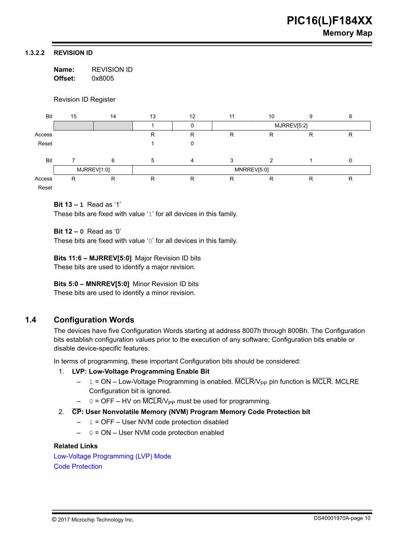
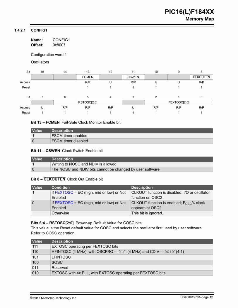
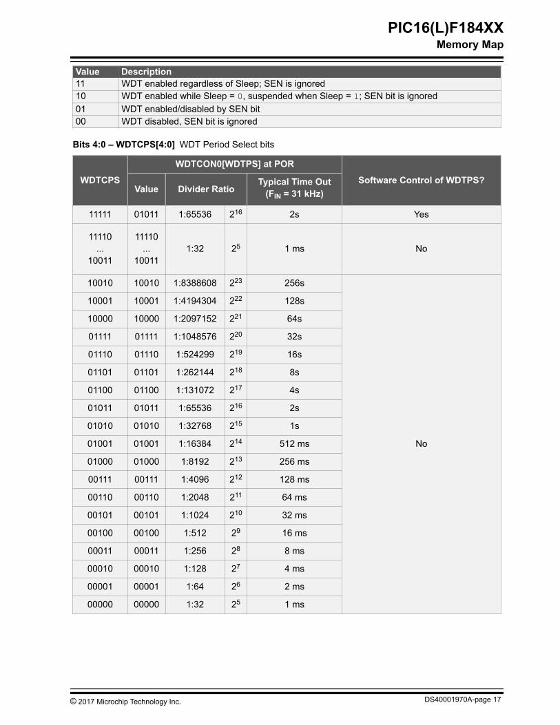
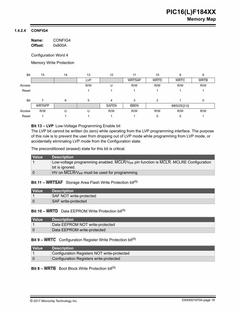
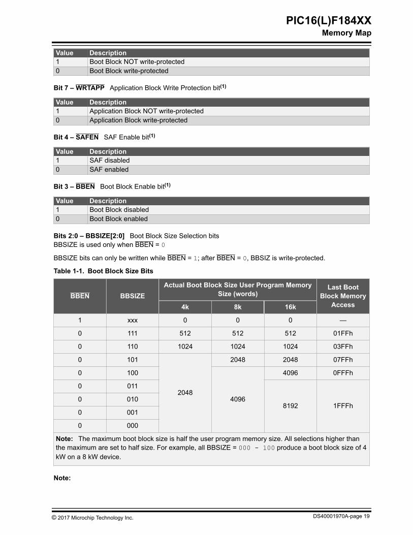
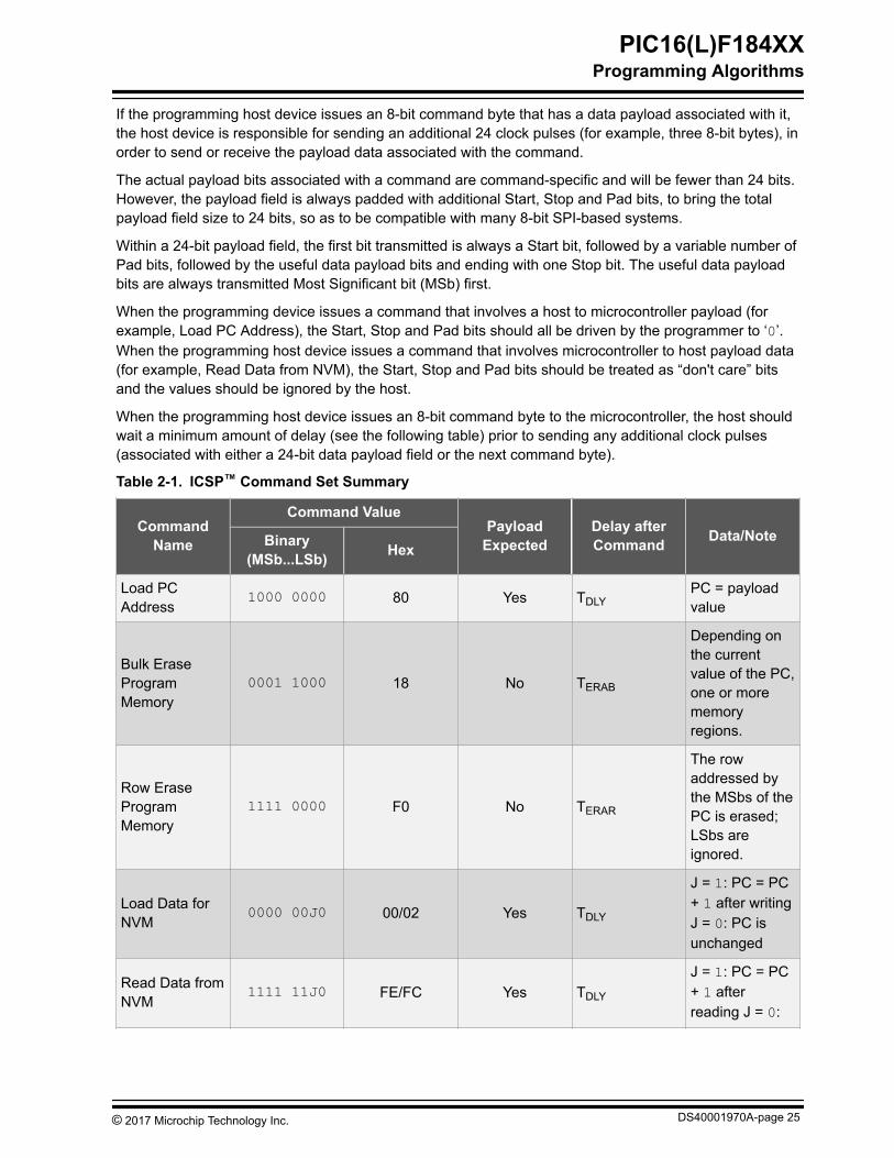
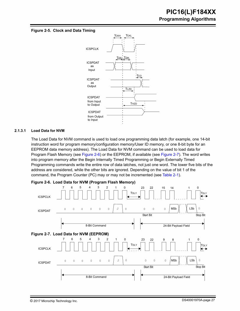
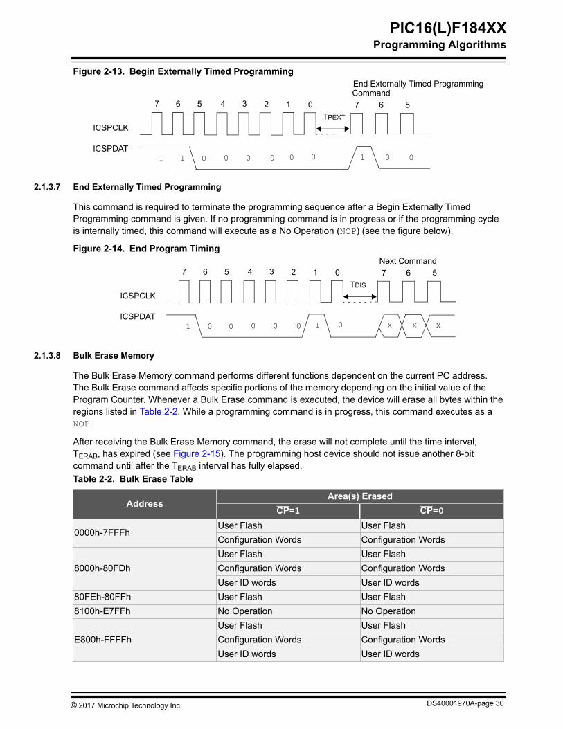

ACDC CHARACTERISTICS Standard Operating Conditions Production tested at 25degC
Sym Characteristics Min Typ Max Units ConditionsComments
TDLY
Data Input not Driven To Next ClockInput (delay required betweencommanddata or commandcommand)
10 mdash mdash micros
TERAB Bulk Erase Cycle Time mdash mdash 84 ms PIC16(L)F184XXdevices
TERAR Row Erase Cycle Time mdash mdash 28 ms
TPINTInternally Timed ProgrammingOperation Time
mdash mdash 28 ms Program memoryConfiguration Wordsmdash mdash 56 ms
TPEXT
Delay Required between BeginExternally Timed Programming andEnd Externally Timed ProgrammingCommands
10 mdash 21 ms (Note 3)
TDISDelay Required after End ExternallyTimed Programming Command 300 mdash mdash micros
TEXITTime Delay when Exiting ProgramVerify Mode 1 mdash mdash micros
Note 1 In case of Bulk Erase the devices default to brown-out enabled with BORV = 1 (low trip point) In order to
ensure that the device is not held in Brown-out Reset VDDMIN becomes the VBOR threshold (with BORV = 1)when performing low-voltage programming on a Bulk Erased device
2 Bulk Erase operation overrides the BOR setting and the minimum VBE threshold is the same for F and LFdevices Refer to the microcontroller data sheet specification for the exact value of VBORMAX
3 Externally timed writes are not supported for Configuration bits
PIC16(L)F184XXProgramming Algorithms
copy 2017 Microchip Technology Inc DS40001970A-page 40
3 Appendix A Revision History (122017)Initial release of this document
PIC16(L)F184XXAppendix A Revision History (122017)
copy 2017 Microchip Technology Inc DS40001970A-page 41
4 Appendix B Device ID Checksums and Pinout Descriptions
41 Device IDs and Checksums
Device DeviceID
Config 1 Config 2 Config 3 Config 4 Config 5 ChecksumW
ord
(HEX
)
Mas
k (H
EX)
Wor
d (H
EX)
Mas
k (H
EX)
Wor
d (H
EX)
Mas
k (H
EX)
Wor
d (H
EX)
Mas
k (H
EX)
Wor
d (u
npro
tect
ed)
Wor
d (p
rote
cted
)
Mas
k
Unprotected Code-protected
Blank(HEX)
00AAhFirstandLast
(HEX)
Blank(HEX)
00AAhFirstandLast
(HEX)
PIC16F18424 30CA 3FFF 2977 3FFF 3EE7 3FFF 3F7F 3FFF 2F9F 3FFF 3FFE 0001 C77D 48D3 9EF9 204FPIC16LF18424 30CB 3FFF 2977 3FFF 3EE7 3FFF 3F7F 3FFF 2F9F 3FFF 3FFE 0001 C77D 48D3 9EF9 204FPIC16F18425 30CC 3FFF 2977 3FFF 3EE7 3FFF 3F7F 3FFF 2F9F 3FFF 3FFE 0001 B77D 38D3 8EF9 104FPIC16LF18425 30CD 3FFF 2977 3FFF 3EE7 3FFF 3F7F 3FFF 2F9F 3FFF 3FFE 0001 B77D 38D3 8EF9 104FPIC16F18426 30D2 3FFF 2977 3FFF 3EE7 3FFF 3F7F 3FFF 2F9F 3FFF 3FFE 0001 977D 18D3 6EF9 F04FPIC16LF18426 30D3 3FFF 2977 3FFF 3EE7 3FFF 3F7F 3FFF 2F9F 3FFF 3FFE 0001 977D 18D3 6EF9 F04FPIC16F18444 30CE 3FFF 2977 3FFF 3EE7 3FFF 3F7F 3FFF 2F9F 3FFF 3FFE 0001 C77D 48D3 9EF9 204FPIC16LF18444 30CF 3FFF 2977 3FFF 3EE7 3FFF 3F7F 3FFF 2F9F 3FFF 3FFE 0001 C77D 48D3 9EF9 204FPIC16F18445 30D0 3FFF 2977 3FFF 3EE7 3FFF 3F7F 3FFF 2F9F 3FFF 3FFE 0001 B77D 38D3 8EF9 104FPIC16LF18445 30D1 3FFF 2977 3FFF 3EE7 3FFF 3F7F 3FFF 2F9F 3FFF 3FFE 0001 B77D 38D3 8EF9 104FPIC16F18446 30D4 3FFF 2977 3FFF 3EE7 3FFF 3F7F 3FFF 2F9F 3FFF 3FFE 0001 977D 18D3 6EF9 F04FPIC16LF18446 30D5 3FFF 2977 3FFF 3EE7 3FFF 3F7F 3FFF 2F9F 3FFF 3FFE 0001 977D 18D3 6EF9 F04FPIC16F18455 30D7 3FFF 2977 3FFF 3EE7 3FFF 3F7F 3FFF 2F9F 3FFF 3FFE 0001 B77D 38D3 8EF9 104FPIC16LF18455 30D8 3FFF 2977 3FFF 3EE7 3FFF 3F7F 3FFF 2F9F 3FFF 3FFE 0001 B77D 38D3 8EF9 104FPIC16F18456 30D9 3FFF 2977 3FFF 3EE7 3FFF 3F7F 3FFF 2F9F 3FFF 3FFE 0001 977D 18D3 6EF9 F04FPIC16LF18456 30DA 3FFF 2977 3FFF 3EE7 3FFF 3F7F 3FFF 2F9F 3FFF 3FFE 0001 977D 18D3 6EF9 F04F
42 Example Checksum Computed with Program Code Protection Disabled BlankDevice
Device Sum of Memory addresses0000h-0FFFh
F000h (1000h3FFFh)
PIC16F18424
Configuration Word 1 3FFFh
Configuration Word 1 mask 2977h
Configuration Word 2 3FFFh
Configuration Word 2 mask 3EE7h
Configuration Word 3 3FFFh
Configuration Word 3 mask 3F7Fh
Configuration Word 4 3FFFh
PIC16(L)F184XXAppendix B Device ID Checksums and Pinou
copy 2017 Microchip Technology Inc DS40001970A-page 42
Device Sum of Memory addresses0000h-0FFFh
F000h (1000h3FFFh)
Configuration Word 4 mask 2F9Fh
Configuration Word 5 Unprotected 3FFFh
Configuration Word 5 mask 0001h
Checksum = F000h + (3FFFh and 2977h) + (3FFFh and3EE7h) + (3FFFh and 3F7Fh) + (3FFFh and2F9Fh) + (3FFFh and 0001h)
= F000h + 2977h + 3EE7h + 3F7Fh + 2F9Fh+ 0001h
= C77Dh
43 Example Checksum Computed with Program Code Protection Disabled 00AAhat First and Last Address
Device Sum of Memory addresses0000h-0FFFh
7156h (AAh + (FFEh3FFFh) + AAh)
PIC16F18424
Configuration Word 1 3FFFh
Configuration Word 1 mask 2977h
Configuration Word 2 3FFFh
Configuration Word 2 mask 3EE7h
Configuration Word 3 3FFFh
Configuration Word 3 mask 3F7Fh
Configuration Word 4 3FFFh
Configuration Word 4 mask 2F9Fh
Configuration Word 5 Unprotected 3FFFh
Configuration Word 5 mask 0001h
Checksum = 7156h + (3FFFh and 2977h) + (3FFFh and3EE7h) + (3FFFh and 3F7Fh) + (3FFFh and2F9Fh) + (3FFFh and 0001h)
= 7156h + 2977h + 3EE7h + 3F7Fh + 2F9Fh+ 0001h
= 48D3h
PIC16(L)F184XXAppendix B Device ID Checksums and Pinou
copy 2017 Microchip Technology Inc DS40001970A-page 43
44 Example Checksum Computed with Program Code Protection Enabled BlankDeviceDevice
PIC16F18424
Configuration Word 1 3FFFh
Configuration Word 1 mask 2977h
Configuration Word 2 3FFFh
Configuration Word 2 mask 3EE7h
Configuration Word 3 3FFFh
Configuration Word 3 mask 3F7Fh
Configuration Word 4 3FFFh
Configuration Word 4 mask 2F9Fh
Configuration Word 5 Unprotected 3FFFh
Configuration Word 5 mask 0001h
Sum of User IDs = (000Ch and 000Fh) ltlt 12 + (0007h and 000Fh) ltlt8 + (0007h and 000Fh) ltlt 4 + (000Dh and 000Fh)
= C000h + 0700h + 0070h + 000Dh
= C77Dh
Checksum = (3FFFh and 2977h) + (3FFFh and 3EE7h)+ (3FFFh and 3F7Fh) + (3FFFh and 2F9Fh)+ (3FFEh and 0001h) + C77Dh
= 2977h + 3EE7h + 3F7Fh + 2F9Fh + 0000h +C77Dh
= 9EF9h
Related LinksProgram Code Protection Enabled
45 Example Checksum Computed with Program Code Protection Enabled 00AAh atFirst and Last AddressDevice
PIC16F18424
Configuration Word 1 3FFFh
Configuration Word 1 mask 2977h
Configuration Word 2 3FFFh
Configuration Word 2 mask 3EE7h
Configuration Word 3 3FFFh
PIC16(L)F184XXAppendix B Device ID Checksums and Pinou
copy 2017 Microchip Technology Inc DS40001970A-page 44
Device
Configuration Word 3 mask 3F7Fh
Configuration Word 4 3FFFh
Configuration Word 4 mask 2F9Fh
Configuration Word 5 Unprotected 3FFFh
Configuration Word 5 mask 0001h
Sum of User IDs (0004h and 000Fh) ltlt 12 + (0008h and 000Fh) ltlt 8+ (000Dh and 000Fh) ltlt 4 + (0003h and 000Fh)
= 4000h + 0800h + 00D0h + 0003h
= 48D3h
Checksum = (3FFFh and 2977h) + (3FFFh and 3EE7h)+ (3FFFh and 3F7Fh) + (3FFFh and 2F9Fh)+ (3FFEh and 0001h) + 48D3h
= 2977h + 3EE7h + 3F7Fh + 2F9Fh + 0000h+ 48D3h
= 204Fh
Related LinksProgram Code Protection Enabled
46 Programming Pin Locations by Package Type
Device PackageType
PkgCode
PackageDrawing
Number(1)VDDPIN
VSSPIN
MCLR ICSPCLK ICSPDAT
PIN PORT PIN PORT PIN PORT
PIC16(L)F18424PIC16(L)F18425PIC16(L)F18426
14 - PDIP (P) C04-005 1 14 4 RA3 12 RA1 13 RA014 - SOIC(39mm) (SL) C04-065 1 14 4 RA3 12 RA1 13 RA0
14 - TSSOP (ST) C04-087 1 14 4 RA3 12 RA1 13 RA016 - uQFN(4x4) (JQ) C04-257 16 13 3 RA3 11 RA1 12 RA0
PIC16(L)F18444PIC16(L)F18445PIC16(L)F18446
20 - PDIP (P) C04-019 1 20 4 RA3 18 RA1 19 RA020 - SOIC (SO) C04-094 1 20 4 RA3 18 RA1 19 RA020 - SSOP (SS) C04-072 1 20 4 RA3 18 RA1 19 RA020 - uQFN(4x4) (GZ) C04-255 18 17 1 RA3 15 RA1 16 RA0
PIC16(L)F18455PIC16(L)F18456
28 - SPDIP (SP) C04-070 20 19 1 RE3 27 RB6 28 RB728 - SSOP (SS) C04-073 20 19 1 RE3 27 RB6 28 RB728 - SOIC (SO) C04-052 20 19 1 RE3 27 RB6 28 RB728 - uQFN(4x4) (MV) C04-152 17 16 26 RE3 24 RB6 25 RB7
Note
PIC16(L)F184XXAppendix B Device ID Checksums and Pinou
copy 2017 Microchip Technology Inc DS40001970A-page 45
Device PackageType
PkgCode
PackageDrawing
Number(1)VDDPIN
VSSPIN
MCLR ICSPCLK ICSPDAT
PIN PORT PIN PORT PIN PORT
1 The most current package drawings can be found in the Microchip Packaging Specification DS00049 found at httpwwwmicrochipcompackaging The drawing numbers listed above do not include the current revision designator whichis added at the end of the number
PIC16(L)F184XXAppendix B Device ID Checksums and Pinou
copy 2017 Microchip Technology Inc DS40001970A-page 46
5 Appendix C Device Configuration Information (DCI)Table 5-1 Device Configuration Information
Address Description Value Units
8200h Erase Row Size 32 Words
8201h Number of WriteLatches
32 mdash
8202h Number of User Rows See Table 5-2 Rows
8203h EE Data Memory Size 256 Bytes
8204h Pin Count See Table 5-3 Pins
Table 5-2 Number of User Rows
Part Name Memory Size Number of User Rows
PIC16(L)F1842418444 4k 128
PIC16(L)F184251844518455 8k 256
PIC16(L)F184261844618456 16k 512
Table 5-3 Pin Count
Part Number Pin Count
PIC16(L)F184242526 14(1)
PIC16(L)F184444546 20
PIC16(L)F1845518456 28
Note 1 16 pin-count devices will show lsquo14rsquo in location 8204h
PIC16(L)F184XXAppendix C Device Configuration Informati
copy 2017 Microchip Technology Inc DS40001970A-page 47
6 Appendix D Device Information Area (DIA)Table 6-1 Device Information Area Address Locations and Descriptions
Address Range Standard Device Information Description8100h 8108h Microchip Unique Identifier (MUI) Unique indentifier based on silicon die information
8109h Reserved Reserved810Ah 8111h External Unique Indentifier (EUI) Optional area for placing customer-specific data
8112h Unassigned Unassigned
8113h Temp Sensor (Low-Range setting) 90degC
ADC conversion data of the Temperature Sensor(Low-Range setting) at 90degC setpoint VDD = 30V VREF
+ = 2048 from FVR18114h Reserved Reserved8115h Unassigned Unassigned
8116h Temp Sensor (High-Range setting) 90degC
ADC conversion data of the Temperature Sensor(High-Range setting) at 90degC setpoint VDD = 30VVREF+ = 2048 from FVR1
8117h Reserved Reserved8118h ADC FVR1 Output Voltage for 1x setting FVR1 1x measured output voltage (mV)8119h ADC FVR1 Output Voltage for 2x setting FVR1 2x measured output voltage (mV)811Ah ADC FVR1 Output Voltage for 4x setting FVR1 4x measured output voltage (mV)811Bh CMP FVR2 Output Voltage for 1x setting FVR2 1x measured output voltage (mV)811Ch CMP FVR2 Output Voltage for 2x setting FVR2 2x measured output voltage (mV)811Dh CMP FVR2 Output Voltage for 4x setting FVR2 4x measured output voltage (mV)
811Eh 811Fh Reserved Reserved
PIC16(L)F184XXAppendix D Device Information Area (DIA)
copy 2017 Microchip Technology Inc DS40001970A-page 48
The Microchip Web Site
Microchip provides online support via our web site at httpwwwmicrochipcom This web site is used asa means to make files and information easily available to customers Accessible by using your favoriteInternet browser the web site contains the following information
bull Product Support ndash Data sheets and errata application notes and sample programs designresources userrsquos guides and hardware support documents latest software releases and archivedsoftware
bull General Technical Support ndash Frequently Asked Questions (FAQ) technical support requestsonline discussion groups Microchip consultant program member listing
bull Business of Microchip ndash Product selector and ordering guides latest Microchip press releaseslisting of seminars and events listings of Microchip sales offices distributors and factoryrepresentatives
Customer Change Notification Service
Microchiprsquos customer notification service helps keep customers current on Microchip productsSubscribers will receive e-mail notification whenever there are changes updates revisions or erratarelated to a specified product family or development tool of interest
To register access the Microchip web site at httpwwwmicrochipcom Under ldquoSupportrdquo click onldquoCustomer Change Notificationrdquo and follow the registration instructions
Customer Support
Users of Microchip products can receive assistance through several channels
bull Distributor or Representativebull Local Sales Officebull Field Application Engineer (FAE)bull Technical Support
Customers should contact their distributor representative or Field Application Engineer (FAE) for supportLocal sales offices are also available to help customers A listing of sales offices and locations is includedin the back of this document
Technical support is available through the web site at httpwwwmicrochipcomsupport
Microchip Devices Code Protection Feature
Note the following details of the code protection feature on Microchip devices
bull Microchip products meet the specification contained in their particular Microchip Data Sheetbull Microchip believes that its family of products is one of the most secure families of its kind on the
market today when used in the intended manner and under normal conditionsbull There are dishonest and possibly illegal methods used to breach the code protection feature All of
these methods to our knowledge require using the Microchip products in a manner outside theoperating specifications contained in Microchiprsquos Data Sheets Most likely the person doing so isengaged in theft of intellectual property
bull Microchip is willing to work with the customer who is concerned about the integrity of their code
PIC16(L)F184XX
copy 2017 Microchip Technology Inc DS40001970A-page 49
bull Neither Microchip nor any other semiconductor manufacturer can guarantee the security of theircode Code protection does not mean that we are guaranteeing the product as ldquounbreakablerdquo
Code protection is constantly evolving We at Microchip are committed to continuously improving thecode protection features of our products Attempts to break Microchiprsquos code protection feature may be aviolation of the Digital Millennium Copyright Act If such acts allow unauthorized access to your softwareor other copyrighted work you may have a right to sue for relief under that Act
Legal Notice
Information contained in this publication regarding device applications and the like is provided only foryour convenience and may be superseded by updates It is your responsibility to ensure that yourapplication meets with your specifications MICROCHIP MAKES NO REPRESENTATIONS ORWARRANTIES OF ANY KIND WHETHER EXPRESS OR IMPLIED WRITTEN OR ORAL STATUTORYOR OTHERWISE RELATED TO THE INFORMATION INCLUDING BUT NOT LIMITED TO ITSCONDITION QUALITY PERFORMANCE MERCHANTABILITY OR FITNESS FOR PURPOSEMicrochip disclaims all liability arising from this information and its use Use of Microchip devices in lifesupport andor safety applications is entirely at the buyerrsquos risk and the buyer agrees to defendindemnify and hold harmless Microchip from any and all damages claims suits or expenses resultingfrom such use No licenses are conveyed implicitly or otherwise under any Microchip intellectualproperty rights unless otherwise stated
Trademarks
The Microchip name and logo the Microchip logo AnyRate AVR AVR logo AVR Freaks BeaconThingsBitCloud CryptoMemory CryptoRF dsPIC FlashFlex flexPWR Heldo JukeBlox KeeLoq KeeLoq logoKleer LANCheck LINK MD maXStylus maXTouch MediaLB megaAVR MOST MOST logo MPLABOptoLyzer PIC picoPower PICSTART PIC32 logo Prochip Designer QTouch RightTouch SAM-BASpyNIC SST SST Logo SuperFlash tinyAVR UNIO and XMEGA are registered trademarks ofMicrochip Technology Incorporated in the USA and other countries
ClockWorks The Embedded Control Solutions Company EtherSynch Hyper Speed Control HyperLightLoad IntelliMOS mTouch Precision Edge and Quiet-Wire are registered trademarks of MicrochipTechnology Incorporated in the USA
Adjacent Key Suppression AKS Analog-for-the-Digital Age Any Capacitor AnyIn AnyOut BodyComchipKIT chipKIT logo CodeGuard CryptoAuthentication CryptoCompanion CryptoControllerdsPICDEM dsPICDEMnet Dynamic Average Matching DAM ECAN EtherGREEN In-Circuit SerialProgramming ICSP Inter-Chip Connectivity JitterBlocker KleerNet KleerNet logo Mindi MiWimotorBench MPASM MPF MPLAB Certified logo MPLIB MPLINK MultiTRAK NetDetach OmniscientCode Generation PICDEM PICDEMnet PICkit PICtail PureSilicon QMatrix RightTouch logo REALICE Ripple Blocker SAM-ICE Serial Quad IO SMART-IS SQI SuperSwitcher SuperSwitcher II TotalEndurance TSHARC USBCheck VariSense ViewSpan WiperLock Wireless DNA and ZENA aretrademarks of Microchip Technology Incorporated in the USA and other countries
SQTP is a service mark of Microchip Technology Incorporated in the USA
Silicon Storage Technology is a registered trademark of Microchip Technology Inc in other countries
GestIC is a registered trademark of Microchip Technology Germany II GmbH amp Co KG a subsidiary ofMicrochip Technology Inc in other countries
All other trademarks mentioned herein are property of their respective companies
PIC16(L)F184XX
copy 2017 Microchip Technology Inc DS40001970A-page 50
copy 2017 Microchip Technology Incorporated Printed in the USA All Rights Reserved
ISBN 978-1-5224-2445-1
Quality Management System Certified by DNV
ISOTS 16949Microchip received ISOTS-169492009 certification for its worldwide headquarters design and waferfabrication facilities in Chandler and Tempe Arizona Gresham Oregon and design centers in Californiaand India The Companyrsquos quality system processes and procedures are for its PICreg MCUs and dsPICreg
DSCs KEELOQreg code hopping devices Serial EEPROMs microperipherals nonvolatile memory andanalog products In addition Microchiprsquos quality system for the design and manufacture of developmentsystems is ISO 90012000 certified
PIC16(L)F184XX
copy 2017 Microchip Technology Inc DS40001970A-page 51
AMERICAS ASIAPACIFIC ASIAPACIFIC EUROPECorporate Office2355 West Chandler BlvdChandler AZ 85224-6199Tel 480-792-7200Fax 480-792-7277Technical SupporthttpwwwmicrochipcomsupportWeb AddresswwwmicrochipcomAtlantaDuluth GATel 678-957-9614Fax 678-957-1455Austin TXTel 512-257-3370BostonWestborough MATel 774-760-0087Fax 774-760-0088ChicagoItasca ILTel 630-285-0071Fax 630-285-0075DallasAddison TXTel 972-818-7423Fax 972-818-2924DetroitNovi MITel 248-848-4000Houston TXTel 281-894-5983IndianapolisNoblesville INTel 317-773-8323Fax 317-773-5453Tel 317-536-2380Los AngelesMission Viejo CATel 949-462-9523Fax 949-462-9608Tel 951-273-7800Raleigh NCTel 919-844-7510New York NYTel 631-435-6000San Jose CATel 408-735-9110Tel 408-436-4270Canada - TorontoTel 905-695-1980Fax 905-695-2078
Australia - SydneyTel 61-2-9868-6733China - BeijingTel 86-10-8569-7000China - ChengduTel 86-28-8665-5511China - ChongqingTel 86-23-8980-9588China - DongguanTel 86-769-8702-9880China - GuangzhouTel 86-20-8755-8029China - HangzhouTel 86-571-8792-8115China - Hong Kong SARTel 852-2943-5100China - NanjingTel 86-25-8473-2460China - QingdaoTel 86-532-8502-7355China - ShanghaiTel 86-21-3326-8000China - ShenyangTel 86-24-2334-2829China - ShenzhenTel 86-755-8864-2200China - SuzhouTel 86-186-6233-1526China - WuhanTel 86-27-5980-5300China - XianTel 86-29-8833-7252China - XiamenTel 86-592-2388138China - ZhuhaiTel 86-756-3210040
India - BangaloreTel 91-80-3090-4444India - New DelhiTel 91-11-4160-8631India - PuneTel 91-20-4121-0141Japan - OsakaTel 81-6-6152-7160Japan - TokyoTel 81-3-6880- 3770Korea - DaeguTel 82-53-744-4301Korea - SeoulTel 82-2-554-7200Malaysia - Kuala LumpurTel 60-3-7651-7906Malaysia - PenangTel 60-4-227-8870Philippines - ManilaTel 63-2-634-9065SingaporeTel 65-6334-8870Taiwan - Hsin ChuTel 886-3-577-8366Taiwan - KaohsiungTel 886-7-213-7830Taiwan - TaipeiTel 886-2-2508-8600Thailand - BangkokTel 66-2-694-1351Vietnam - Ho Chi MinhTel 84-28-5448-2100
Austria - WelsTel 43-7242-2244-39Fax 43-7242-2244-393Denmark - CopenhagenTel 45-4450-2828Fax 45-4485-2829Finland - EspooTel 358-9-4520-820France - ParisTel 33-1-69-53-63-20Fax 33-1-69-30-90-79Germany - GarchingTel 49-8931-9700Germany - HaanTel 49-2129-3766400Germany - HeilbronnTel 49-7131-67-3636Germany - KarlsruheTel 49-721-625370Germany - MunichTel 49-89-627-144-0Fax 49-89-627-144-44Germany - RosenheimTel 49-8031-354-560Israel - RarsquoananaTel 972-9-744-7705Italy - MilanTel 39-0331-742611Fax 39-0331-466781Italy - PadovaTel 39-049-7625286Netherlands - DrunenTel 31-416-690399Fax 31-416-690340Norway - TrondheimTel 47-7289-7561Poland - WarsawTel 48-22-3325737Romania - BucharestTel 40-21-407-87-50Spain - MadridTel 34-91-708-08-90Fax 34-91-708-08-91Sweden - GothenbergTel 46-31-704-60-40Sweden - StockholmTel 46-8-5090-4654UK - WokinghamTel 44-118-921-5800Fax 44-118-921-5820
Worldwide Sales and Service
copy 2017 Microchip Technology Inc DS40001970A-page 52
- Overview
- Programming Data Flow
- Write andor Erase Selection
-
- 1 Erasing Memory
- 2 Writing Memory
- 3 Multi-Word Programming Interface
-
- Hardware Requirements
-
- 1 High-Voltage ICSP Programming
- 2 Low-Voltage ICSP Programming
-
- 21 Single-Supply ICSP Programming
-
- Pin Utilization
- Table of Contents
- 1 Memory Map
-
- 11 Program Memory Mapping
- 12 User ID Location
- 13 DeviceRevision ID
-
- 131 Register Summary - Device and Revision
- 132 Register Definitions Device and Revision
-
- 1321 DEVICE ID
- 1322 REVISION ID
-
- 14 Configuration Words
-
- 141 Register Summary - Configuration Words
- 142 Register Definitions Configuration Words
-
- 1421 CONFIG1
- 1422 CONFIG2
- 1423 CONFIG3
- 1424 CONFIG4
- 1425 CONFIG5
-
- 15 Device Information Area
- 16 Device Configuration Information
-
- 2 Programming Algorithms
-
- 21 ProgramVerify Mode
-
- 211 High-Voltage ProgramVerify Mode Entry and Exit
-
- 2111 VPP ndash First Entry Mode
- 2112 VDD ndash First Entry Mode
- 2113 ProgramVerify Mode Exit
-
- 212 Low-Voltage Programming (LVP) Mode
- 213 ProgramVerify Commands
-
- 2131 Load Data for NVM
- 2132 Read Data from NVM
- 2133 Load PC Address
- 2134 Increment Address
- 2135 Begin Internally Timed Programming
- 2136 Begin Externally Timed Programming
- 2137 End Externally Timed Programming
- 2138 Bulk Erase Memory
- 2139 Row Erase Memory
-
- 22 Programming Algorithms
- 23 Code Protection
-
- 231 Program Memory
-
- 24 Hex File Usage
-
- 241 Configuration Word
- 242 Device ID
- 243 Checksum Computation
-
- 2431 Program Code Protection Disabled
- 2432 Program Code Protection Enabled
-
- 25 Electrical Specifications
-
- 3 Appendix A Revision History (122017)
- 4 Appendix B Device ID Checksums and Pinout Descriptions
-
- 41 Device IDs and Checksums
- 42 Example Checksum Computed with Program Code Protection Disabled Blank Device
- 43 Example Checksum Computed with Program Code Protection Disabled 00AAh at First and Last Address
- 44 Example Checksum Computed with Program Code Protection Enabled Blank Device
- 45 Example Checksum Computed with Program Code Protection Enabled 00AAh at First and Last Address
- 46 Programming Pin Locations by Package Type
-
- 5 Appendix C Device Configuration Information (DCI)
- 6 Appendix D Device Information Area (DIA)
- The Microchip Web Site
- Customer Change Notification Service
- Customer Support
- Microchip Devices Code Protection Feature
- Legal Notice
- Trademarks
- Quality Management System Certified by DNV
- Worldwide Sales and Service
-

Device Sum of Memory addresses0000h-0FFFh
F000h (1000h3FFFh)
Configuration Word 4 mask 2F9Fh
Configuration Word 5 Unprotected 3FFFh
Configuration Word 5 mask 0001h
Checksum = F000h + (3FFFh and 2977h) + (3FFFh and3EE7h) + (3FFFh and 3F7Fh) + (3FFFh and2F9Fh) + (3FFFh and 0001h)
= F000h + 2977h + 3EE7h + 3F7Fh + 2F9Fh+ 0001h
= C77Dh
43 Example Checksum Computed with Program Code Protection Disabled 00AAhat First and Last Address
Device Sum of Memory addresses0000h-0FFFh
7156h (AAh + (FFEh3FFFh) + AAh)
PIC16F18424
Configuration Word 1 3FFFh
Configuration Word 1 mask 2977h
Configuration Word 2 3FFFh
Configuration Word 2 mask 3EE7h
Configuration Word 3 3FFFh
Configuration Word 3 mask 3F7Fh
Configuration Word 4 3FFFh
Configuration Word 4 mask 2F9Fh
Configuration Word 5 Unprotected 3FFFh
Configuration Word 5 mask 0001h
Checksum = 7156h + (3FFFh and 2977h) + (3FFFh and3EE7h) + (3FFFh and 3F7Fh) + (3FFFh and2F9Fh) + (3FFFh and 0001h)
= 7156h + 2977h + 3EE7h + 3F7Fh + 2F9Fh+ 0001h
= 48D3h
PIC16(L)F184XXAppendix B Device ID Checksums and Pinou
copy 2017 Microchip Technology Inc DS40001970A-page 43
44 Example Checksum Computed with Program Code Protection Enabled BlankDeviceDevice
PIC16F18424
Configuration Word 1 3FFFh
Configuration Word 1 mask 2977h
Configuration Word 2 3FFFh
Configuration Word 2 mask 3EE7h
Configuration Word 3 3FFFh
Configuration Word 3 mask 3F7Fh
Configuration Word 4 3FFFh
Configuration Word 4 mask 2F9Fh
Configuration Word 5 Unprotected 3FFFh
Configuration Word 5 mask 0001h
Sum of User IDs = (000Ch and 000Fh) ltlt 12 + (0007h and 000Fh) ltlt8 + (0007h and 000Fh) ltlt 4 + (000Dh and 000Fh)
= C000h + 0700h + 0070h + 000Dh
= C77Dh
Checksum = (3FFFh and 2977h) + (3FFFh and 3EE7h)+ (3FFFh and 3F7Fh) + (3FFFh and 2F9Fh)+ (3FFEh and 0001h) + C77Dh
= 2977h + 3EE7h + 3F7Fh + 2F9Fh + 0000h +C77Dh
= 9EF9h
Related LinksProgram Code Protection Enabled
45 Example Checksum Computed with Program Code Protection Enabled 00AAh atFirst and Last AddressDevice
PIC16F18424
Configuration Word 1 3FFFh
Configuration Word 1 mask 2977h
Configuration Word 2 3FFFh
Configuration Word 2 mask 3EE7h
Configuration Word 3 3FFFh
PIC16(L)F184XXAppendix B Device ID Checksums and Pinou
copy 2017 Microchip Technology Inc DS40001970A-page 44
Device
Configuration Word 3 mask 3F7Fh
Configuration Word 4 3FFFh
Configuration Word 4 mask 2F9Fh
Configuration Word 5 Unprotected 3FFFh
Configuration Word 5 mask 0001h
Sum of User IDs (0004h and 000Fh) ltlt 12 + (0008h and 000Fh) ltlt 8+ (000Dh and 000Fh) ltlt 4 + (0003h and 000Fh)
= 4000h + 0800h + 00D0h + 0003h
= 48D3h
Checksum = (3FFFh and 2977h) + (3FFFh and 3EE7h)+ (3FFFh and 3F7Fh) + (3FFFh and 2F9Fh)+ (3FFEh and 0001h) + 48D3h
= 2977h + 3EE7h + 3F7Fh + 2F9Fh + 0000h+ 48D3h
= 204Fh
Related LinksProgram Code Protection Enabled
46 Programming Pin Locations by Package Type
Device PackageType
PkgCode
PackageDrawing
Number(1)VDDPIN
VSSPIN
MCLR ICSPCLK ICSPDAT
PIN PORT PIN PORT PIN PORT
PIC16(L)F18424PIC16(L)F18425PIC16(L)F18426
14 - PDIP (P) C04-005 1 14 4 RA3 12 RA1 13 RA014 - SOIC(39mm) (SL) C04-065 1 14 4 RA3 12 RA1 13 RA0
14 - TSSOP (ST) C04-087 1 14 4 RA3 12 RA1 13 RA016 - uQFN(4x4) (JQ) C04-257 16 13 3 RA3 11 RA1 12 RA0
PIC16(L)F18444PIC16(L)F18445PIC16(L)F18446
20 - PDIP (P) C04-019 1 20 4 RA3 18 RA1 19 RA020 - SOIC (SO) C04-094 1 20 4 RA3 18 RA1 19 RA020 - SSOP (SS) C04-072 1 20 4 RA3 18 RA1 19 RA020 - uQFN(4x4) (GZ) C04-255 18 17 1 RA3 15 RA1 16 RA0
PIC16(L)F18455PIC16(L)F18456
28 - SPDIP (SP) C04-070 20 19 1 RE3 27 RB6 28 RB728 - SSOP (SS) C04-073 20 19 1 RE3 27 RB6 28 RB728 - SOIC (SO) C04-052 20 19 1 RE3 27 RB6 28 RB728 - uQFN(4x4) (MV) C04-152 17 16 26 RE3 24 RB6 25 RB7
Note
PIC16(L)F184XXAppendix B Device ID Checksums and Pinou
copy 2017 Microchip Technology Inc DS40001970A-page 45
Device PackageType
PkgCode
PackageDrawing
Number(1)VDDPIN
VSSPIN
MCLR ICSPCLK ICSPDAT
PIN PORT PIN PORT PIN PORT
1 The most current package drawings can be found in the Microchip Packaging Specification DS00049 found at httpwwwmicrochipcompackaging The drawing numbers listed above do not include the current revision designator whichis added at the end of the number
PIC16(L)F184XXAppendix B Device ID Checksums and Pinou
copy 2017 Microchip Technology Inc DS40001970A-page 46
5 Appendix C Device Configuration Information (DCI)Table 5-1 Device Configuration Information
Address Description Value Units
8200h Erase Row Size 32 Words
8201h Number of WriteLatches
32 mdash
8202h Number of User Rows See Table 5-2 Rows
8203h EE Data Memory Size 256 Bytes
8204h Pin Count See Table 5-3 Pins
Table 5-2 Number of User Rows
Part Name Memory Size Number of User Rows
PIC16(L)F1842418444 4k 128
PIC16(L)F184251844518455 8k 256
PIC16(L)F184261844618456 16k 512
Table 5-3 Pin Count
Part Number Pin Count
PIC16(L)F184242526 14(1)
PIC16(L)F184444546 20
PIC16(L)F1845518456 28
Note 1 16 pin-count devices will show lsquo14rsquo in location 8204h
PIC16(L)F184XXAppendix C Device Configuration Informati
copy 2017 Microchip Technology Inc DS40001970A-page 47
6 Appendix D Device Information Area (DIA)Table 6-1 Device Information Area Address Locations and Descriptions
Address Range Standard Device Information Description8100h 8108h Microchip Unique Identifier (MUI) Unique indentifier based on silicon die information
8109h Reserved Reserved810Ah 8111h External Unique Indentifier (EUI) Optional area for placing customer-specific data
8112h Unassigned Unassigned
8113h Temp Sensor (Low-Range setting) 90degC
ADC conversion data of the Temperature Sensor(Low-Range setting) at 90degC setpoint VDD = 30V VREF
+ = 2048 from FVR18114h Reserved Reserved8115h Unassigned Unassigned
8116h Temp Sensor (High-Range setting) 90degC
ADC conversion data of the Temperature Sensor(High-Range setting) at 90degC setpoint VDD = 30VVREF+ = 2048 from FVR1
8117h Reserved Reserved8118h ADC FVR1 Output Voltage for 1x setting FVR1 1x measured output voltage (mV)8119h ADC FVR1 Output Voltage for 2x setting FVR1 2x measured output voltage (mV)811Ah ADC FVR1 Output Voltage for 4x setting FVR1 4x measured output voltage (mV)811Bh CMP FVR2 Output Voltage for 1x setting FVR2 1x measured output voltage (mV)811Ch CMP FVR2 Output Voltage for 2x setting FVR2 2x measured output voltage (mV)811Dh CMP FVR2 Output Voltage for 4x setting FVR2 4x measured output voltage (mV)
811Eh 811Fh Reserved Reserved
PIC16(L)F184XXAppendix D Device Information Area (DIA)
copy 2017 Microchip Technology Inc DS40001970A-page 48
The Microchip Web Site
Microchip provides online support via our web site at httpwwwmicrochipcom This web site is used asa means to make files and information easily available to customers Accessible by using your favoriteInternet browser the web site contains the following information
bull Product Support ndash Data sheets and errata application notes and sample programs designresources userrsquos guides and hardware support documents latest software releases and archivedsoftware
bull General Technical Support ndash Frequently Asked Questions (FAQ) technical support requestsonline discussion groups Microchip consultant program member listing
bull Business of Microchip ndash Product selector and ordering guides latest Microchip press releaseslisting of seminars and events listings of Microchip sales offices distributors and factoryrepresentatives
Customer Change Notification Service
Microchiprsquos customer notification service helps keep customers current on Microchip productsSubscribers will receive e-mail notification whenever there are changes updates revisions or erratarelated to a specified product family or development tool of interest
To register access the Microchip web site at httpwwwmicrochipcom Under ldquoSupportrdquo click onldquoCustomer Change Notificationrdquo and follow the registration instructions
Customer Support
Users of Microchip products can receive assistance through several channels
bull Distributor or Representativebull Local Sales Officebull Field Application Engineer (FAE)bull Technical Support
Customers should contact their distributor representative or Field Application Engineer (FAE) for supportLocal sales offices are also available to help customers A listing of sales offices and locations is includedin the back of this document
Technical support is available through the web site at httpwwwmicrochipcomsupport
Microchip Devices Code Protection Feature
Note the following details of the code protection feature on Microchip devices
bull Microchip products meet the specification contained in their particular Microchip Data Sheetbull Microchip believes that its family of products is one of the most secure families of its kind on the
market today when used in the intended manner and under normal conditionsbull There are dishonest and possibly illegal methods used to breach the code protection feature All of
these methods to our knowledge require using the Microchip products in a manner outside theoperating specifications contained in Microchiprsquos Data Sheets Most likely the person doing so isengaged in theft of intellectual property
bull Microchip is willing to work with the customer who is concerned about the integrity of their code
PIC16(L)F184XX
copy 2017 Microchip Technology Inc DS40001970A-page 49
bull Neither Microchip nor any other semiconductor manufacturer can guarantee the security of theircode Code protection does not mean that we are guaranteeing the product as ldquounbreakablerdquo
Code protection is constantly evolving We at Microchip are committed to continuously improving thecode protection features of our products Attempts to break Microchiprsquos code protection feature may be aviolation of the Digital Millennium Copyright Act If such acts allow unauthorized access to your softwareor other copyrighted work you may have a right to sue for relief under that Act
Legal Notice
Information contained in this publication regarding device applications and the like is provided only foryour convenience and may be superseded by updates It is your responsibility to ensure that yourapplication meets with your specifications MICROCHIP MAKES NO REPRESENTATIONS ORWARRANTIES OF ANY KIND WHETHER EXPRESS OR IMPLIED WRITTEN OR ORAL STATUTORYOR OTHERWISE RELATED TO THE INFORMATION INCLUDING BUT NOT LIMITED TO ITSCONDITION QUALITY PERFORMANCE MERCHANTABILITY OR FITNESS FOR PURPOSEMicrochip disclaims all liability arising from this information and its use Use of Microchip devices in lifesupport andor safety applications is entirely at the buyerrsquos risk and the buyer agrees to defendindemnify and hold harmless Microchip from any and all damages claims suits or expenses resultingfrom such use No licenses are conveyed implicitly or otherwise under any Microchip intellectualproperty rights unless otherwise stated
Trademarks
The Microchip name and logo the Microchip logo AnyRate AVR AVR logo AVR Freaks BeaconThingsBitCloud CryptoMemory CryptoRF dsPIC FlashFlex flexPWR Heldo JukeBlox KeeLoq KeeLoq logoKleer LANCheck LINK MD maXStylus maXTouch MediaLB megaAVR MOST MOST logo MPLABOptoLyzer PIC picoPower PICSTART PIC32 logo Prochip Designer QTouch RightTouch SAM-BASpyNIC SST SST Logo SuperFlash tinyAVR UNIO and XMEGA are registered trademarks ofMicrochip Technology Incorporated in the USA and other countries
ClockWorks The Embedded Control Solutions Company EtherSynch Hyper Speed Control HyperLightLoad IntelliMOS mTouch Precision Edge and Quiet-Wire are registered trademarks of MicrochipTechnology Incorporated in the USA
Adjacent Key Suppression AKS Analog-for-the-Digital Age Any Capacitor AnyIn AnyOut BodyComchipKIT chipKIT logo CodeGuard CryptoAuthentication CryptoCompanion CryptoControllerdsPICDEM dsPICDEMnet Dynamic Average Matching DAM ECAN EtherGREEN In-Circuit SerialProgramming ICSP Inter-Chip Connectivity JitterBlocker KleerNet KleerNet logo Mindi MiWimotorBench MPASM MPF MPLAB Certified logo MPLIB MPLINK MultiTRAK NetDetach OmniscientCode Generation PICDEM PICDEMnet PICkit PICtail PureSilicon QMatrix RightTouch logo REALICE Ripple Blocker SAM-ICE Serial Quad IO SMART-IS SQI SuperSwitcher SuperSwitcher II TotalEndurance TSHARC USBCheck VariSense ViewSpan WiperLock Wireless DNA and ZENA aretrademarks of Microchip Technology Incorporated in the USA and other countries
SQTP is a service mark of Microchip Technology Incorporated in the USA
Silicon Storage Technology is a registered trademark of Microchip Technology Inc in other countries
GestIC is a registered trademark of Microchip Technology Germany II GmbH amp Co KG a subsidiary ofMicrochip Technology Inc in other countries
All other trademarks mentioned herein are property of their respective companies
PIC16(L)F184XX
copy 2017 Microchip Technology Inc DS40001970A-page 50
copy 2017 Microchip Technology Incorporated Printed in the USA All Rights Reserved
ISBN 978-1-5224-2445-1
Quality Management System Certified by DNV
ISOTS 16949Microchip received ISOTS-169492009 certification for its worldwide headquarters design and waferfabrication facilities in Chandler and Tempe Arizona Gresham Oregon and design centers in Californiaand India The Companyrsquos quality system processes and procedures are for its PICreg MCUs and dsPICreg
DSCs KEELOQreg code hopping devices Serial EEPROMs microperipherals nonvolatile memory andanalog products In addition Microchiprsquos quality system for the design and manufacture of developmentsystems is ISO 90012000 certified
PIC16(L)F184XX
copy 2017 Microchip Technology Inc DS40001970A-page 51
AMERICAS ASIAPACIFIC ASIAPACIFIC EUROPECorporate Office2355 West Chandler BlvdChandler AZ 85224-6199Tel 480-792-7200Fax 480-792-7277Technical SupporthttpwwwmicrochipcomsupportWeb AddresswwwmicrochipcomAtlantaDuluth GATel 678-957-9614Fax 678-957-1455Austin TXTel 512-257-3370BostonWestborough MATel 774-760-0087Fax 774-760-0088ChicagoItasca ILTel 630-285-0071Fax 630-285-0075DallasAddison TXTel 972-818-7423Fax 972-818-2924DetroitNovi MITel 248-848-4000Houston TXTel 281-894-5983IndianapolisNoblesville INTel 317-773-8323Fax 317-773-5453Tel 317-536-2380Los AngelesMission Viejo CATel 949-462-9523Fax 949-462-9608Tel 951-273-7800Raleigh NCTel 919-844-7510New York NYTel 631-435-6000San Jose CATel 408-735-9110Tel 408-436-4270Canada - TorontoTel 905-695-1980Fax 905-695-2078
Australia - SydneyTel 61-2-9868-6733China - BeijingTel 86-10-8569-7000China - ChengduTel 86-28-8665-5511China - ChongqingTel 86-23-8980-9588China - DongguanTel 86-769-8702-9880China - GuangzhouTel 86-20-8755-8029China - HangzhouTel 86-571-8792-8115China - Hong Kong SARTel 852-2943-5100China - NanjingTel 86-25-8473-2460China - QingdaoTel 86-532-8502-7355China - ShanghaiTel 86-21-3326-8000China - ShenyangTel 86-24-2334-2829China - ShenzhenTel 86-755-8864-2200China - SuzhouTel 86-186-6233-1526China - WuhanTel 86-27-5980-5300China - XianTel 86-29-8833-7252China - XiamenTel 86-592-2388138China - ZhuhaiTel 86-756-3210040
India - BangaloreTel 91-80-3090-4444India - New DelhiTel 91-11-4160-8631India - PuneTel 91-20-4121-0141Japan - OsakaTel 81-6-6152-7160Japan - TokyoTel 81-3-6880- 3770Korea - DaeguTel 82-53-744-4301Korea - SeoulTel 82-2-554-7200Malaysia - Kuala LumpurTel 60-3-7651-7906Malaysia - PenangTel 60-4-227-8870Philippines - ManilaTel 63-2-634-9065SingaporeTel 65-6334-8870Taiwan - Hsin ChuTel 886-3-577-8366Taiwan - KaohsiungTel 886-7-213-7830Taiwan - TaipeiTel 886-2-2508-8600Thailand - BangkokTel 66-2-694-1351Vietnam - Ho Chi MinhTel 84-28-5448-2100
Austria - WelsTel 43-7242-2244-39Fax 43-7242-2244-393Denmark - CopenhagenTel 45-4450-2828Fax 45-4485-2829Finland - EspooTel 358-9-4520-820France - ParisTel 33-1-69-53-63-20Fax 33-1-69-30-90-79Germany - GarchingTel 49-8931-9700Germany - HaanTel 49-2129-3766400Germany - HeilbronnTel 49-7131-67-3636Germany - KarlsruheTel 49-721-625370Germany - MunichTel 49-89-627-144-0Fax 49-89-627-144-44Germany - RosenheimTel 49-8031-354-560Israel - RarsquoananaTel 972-9-744-7705Italy - MilanTel 39-0331-742611Fax 39-0331-466781Italy - PadovaTel 39-049-7625286Netherlands - DrunenTel 31-416-690399Fax 31-416-690340Norway - TrondheimTel 47-7289-7561Poland - WarsawTel 48-22-3325737Romania - BucharestTel 40-21-407-87-50Spain - MadridTel 34-91-708-08-90Fax 34-91-708-08-91Sweden - GothenbergTel 46-31-704-60-40Sweden - StockholmTel 46-8-5090-4654UK - WokinghamTel 44-118-921-5800Fax 44-118-921-5820
Worldwide Sales and Service
copy 2017 Microchip Technology Inc DS40001970A-page 52
- Overview
- Programming Data Flow
- Write andor Erase Selection
-
- 1 Erasing Memory
- 2 Writing Memory
- 3 Multi-Word Programming Interface
-
- Hardware Requirements
-
- 1 High-Voltage ICSP Programming
- 2 Low-Voltage ICSP Programming
-
- 21 Single-Supply ICSP Programming
-
- Pin Utilization
- Table of Contents
- 1 Memory Map
-
- 11 Program Memory Mapping
- 12 User ID Location
- 13 DeviceRevision ID
-
- 131 Register Summary - Device and Revision
- 132 Register Definitions Device and Revision
-
- 1321 DEVICE ID
- 1322 REVISION ID
-
- 14 Configuration Words
-
- 141 Register Summary - Configuration Words
- 142 Register Definitions Configuration Words
-
- 1421 CONFIG1
- 1422 CONFIG2
- 1423 CONFIG3
- 1424 CONFIG4
- 1425 CONFIG5
-
- 15 Device Information Area
- 16 Device Configuration Information
-
- 2 Programming Algorithms
-
- 21 ProgramVerify Mode
-
- 211 High-Voltage ProgramVerify Mode Entry and Exit
-
- 2111 VPP ndash First Entry Mode
- 2112 VDD ndash First Entry Mode
- 2113 ProgramVerify Mode Exit
-
- 212 Low-Voltage Programming (LVP) Mode
- 213 ProgramVerify Commands
-
- 2131 Load Data for NVM
- 2132 Read Data from NVM
- 2133 Load PC Address
- 2134 Increment Address
- 2135 Begin Internally Timed Programming
- 2136 Begin Externally Timed Programming
- 2137 End Externally Timed Programming
- 2138 Bulk Erase Memory
- 2139 Row Erase Memory
-
- 22 Programming Algorithms
- 23 Code Protection
-
- 231 Program Memory
-
- 24 Hex File Usage
-
- 241 Configuration Word
- 242 Device ID
- 243 Checksum Computation
-
- 2431 Program Code Protection Disabled
- 2432 Program Code Protection Enabled
-
- 25 Electrical Specifications
-
- 3 Appendix A Revision History (122017)
- 4 Appendix B Device ID Checksums and Pinout Descriptions
-
- 41 Device IDs and Checksums
- 42 Example Checksum Computed with Program Code Protection Disabled Blank Device
- 43 Example Checksum Computed with Program Code Protection Disabled 00AAh at First and Last Address
- 44 Example Checksum Computed with Program Code Protection Enabled Blank Device
- 45 Example Checksum Computed with Program Code Protection Enabled 00AAh at First and Last Address
- 46 Programming Pin Locations by Package Type
-
- 5 Appendix C Device Configuration Information (DCI)
- 6 Appendix D Device Information Area (DIA)
- The Microchip Web Site
- Customer Change Notification Service
- Customer Support
- Microchip Devices Code Protection Feature
- Legal Notice
- Trademarks
- Quality Management System Certified by DNV
- Worldwide Sales and Service
-
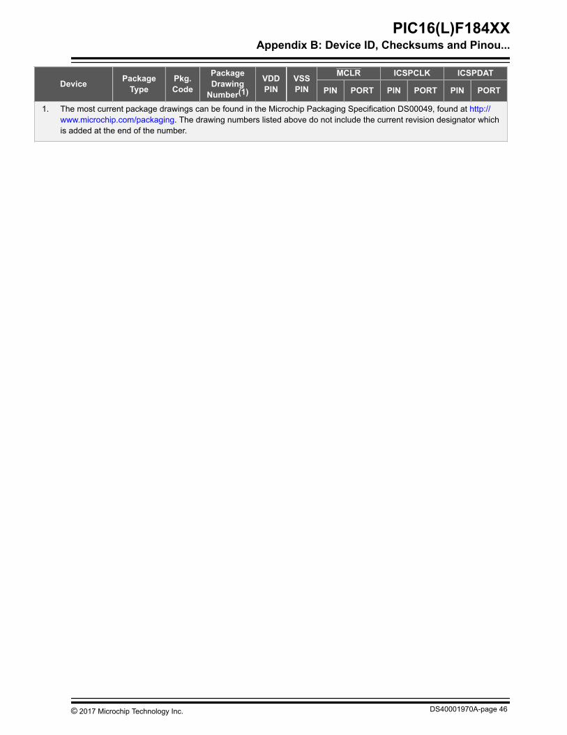
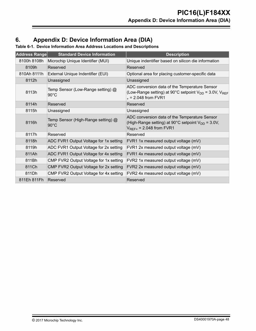