cs 320 computer architecture 8051 core architectureeh60/spring2006/cs 320/term.pdf · computer...
TRANSCRIPT

CS 320
Computer Architecture
8051 Core Architecture
Evan Hallam
19 April 2006

Abstract
The 8051 is an 8-bit microprocessor designed originally in the 1980’s by the Intel Corporation. This inexpen-
sive and simple, yet extremely useful and powerful microprocessor is commonly used in a variety of control
systems, embedded applications and consumer electronics. Although many derivatives of the 8051 exist
that create a versatile set of microprocessors, the core architecture of the entire family remains relatively
unchanged [1]. The basic architectural form of the 8051 will be examined with some references to derivative
models. Primary architecture aspects to be analyzed will include: hardware overview, memory organization,
registers and buffers, instructions and addressing, input/output and the interrupt system.

Contents
1 Introduction 1
2 Hardware Overview 1
2.1 Registers, Ports, Etc. . . . . . . . . . . . . . . . . . . . . . . . . . . . . . . . . . . . . . . . . . 2
2.2 Pinout . . . . . . . . . . . . . . . . . . . . . . . . . . . . . . . . . . . . . . . . . . . . . . . . . 3
2.3 Oscillator and Clocking . . . . . . . . . . . . . . . . . . . . . . . . . . . . . . . . . . . . . . . 4
3 Memory Organization 5
3.1 Memory Space Separation and Size . . . . . . . . . . . . . . . . . . . . . . . . . . . . . . . . . 6
3.2 Program Storage . . . . . . . . . . . . . . . . . . . . . . . . . . . . . . . . . . . . . . . . . . . 6
3.3 Data Storage . . . . . . . . . . . . . . . . . . . . . . . . . . . . . . . . . . . . . . . . . . . . . 6
3.4 On-Chip ROM . . . . . . . . . . . . . . . . . . . . . . . . . . . . . . . . . . . . . . . . . . . . 7
4 Special Function Registers 8
4.1 Accumulator and B Registers . . . . . . . . . . . . . . . . . . . . . . . . . . . . . . . . . . . . 8
4.2 Program Status Word . . . . . . . . . . . . . . . . . . . . . . . . . . . . . . . . . . . . . . . . 9
4.3 Stack Pointer . . . . . . . . . . . . . . . . . . . . . . . . . . . . . . . . . . . . . . . . . . . . . 10
4.4 Program Counter and Data Pointer . . . . . . . . . . . . . . . . . . . . . . . . . . . . . . . . . 10
4.5 Port Latches . . . . . . . . . . . . . . . . . . . . . . . . . . . . . . . . . . . . . . . . . . . . . 10
4.6 Serial Data Buffer . . . . . . . . . . . . . . . . . . . . . . . . . . . . . . . . . . . . . . . . . . 11
4.7 Timer Registers . . . . . . . . . . . . . . . . . . . . . . . . . . . . . . . . . . . . . . . . . . . . 11
4.8 Control Registers . . . . . . . . . . . . . . . . . . . . . . . . . . . . . . . . . . . . . . . . . . . 11
5 I/O Ports 11
5.1 Input Loading and Output Driving . . . . . . . . . . . . . . . . . . . . . . . . . . . . . . . . . 12
5.2 Alternate Port Functions . . . . . . . . . . . . . . . . . . . . . . . . . . . . . . . . . . . . . . 12
5.3 Accessing External Memory . . . . . . . . . . . . . . . . . . . . . . . . . . . . . . . . . . . . . 13
I
6 Timers and Counters 13
6.1 Timing . . . . . . . . . . . . . . . . . . . . . . . . . . . . . . . . . . . . . . . . . . . . . . . . . 14
6.2 Timer 0 and Timer 1 . . . . . . . . . . . . . . . . . . . . . . . . . . . . . . . . . . . . . . . . . 14
6.3 Timer Modes . . . . . . . . . . . . . . . . . . . . . . . . . . . . . . . . . . . . . . . . . . . . . 15
6.3.1 Mode 0 and Mode 1 . . . . . . . . . . . . . . . . . . . . . . . . . . . . . . . . . . . . . 15
6.3.2 Mode 2 . . . . . . . . . . . . . . . . . . . . . . . . . . . . . . . . . . . . . . . . . . . . 16
6.3.3 Mode 3 . . . . . . . . . . . . . . . . . . . . . . . . . . . . . . . . . . . . . . . . . . . . 16
6.4 Timer 2 . . . . . . . . . . . . . . . . . . . . . . . . . . . . . . . . . . . . . . . . . . . . . . . . 16
7 Serial Ports 16
7.1 Serial Port Control and Status Register . . . . . . . . . . . . . . . . . . . . . . . . . . . . . . 17
7.2 Serial Port Modes . . . . . . . . . . . . . . . . . . . . . . . . . . . . . . . . . . . . . . . . . . 18
7.2.1 Mode 0 - Shift Register Mode . . . . . . . . . . . . . . . . . . . . . . . . . . . . . . . . 18
7.2.2 Mode 1 - Standard UART . . . . . . . . . . . . . . . . . . . . . . . . . . . . . . . . . . 18
7.2.3 Mode 2 and Mode 3 - Multiprocessor Modes . . . . . . . . . . . . . . . . . . . . . . . 19
7.3 PCON Register . . . . . . . . . . . . . . . . . . . . . . . . . . . . . . . . . . . . . . . . . . . . 19
8 Interrupts 19
8.1 Servicing External Devices . . . . . . . . . . . . . . . . . . . . . . . . . . . . . . . . . . . . . . 20
8.2 Polling and Buffering . . . . . . . . . . . . . . . . . . . . . . . . . . . . . . . . . . . . . . . . . 21
8.3 Basic Interrupt Action . . . . . . . . . . . . . . . . . . . . . . . . . . . . . . . . . . . . . . . . 21
8.4 Multiple Interrupt Sources and Vectoring . . . . . . . . . . . . . . . . . . . . . . . . . . . . . 21
8.5 Priority Levels . . . . . . . . . . . . . . . . . . . . . . . . . . . . . . . . . . . . . . . . . . . . 22
8.6 Interrupt Timing and Handling . . . . . . . . . . . . . . . . . . . . . . . . . . . . . . . . . . . 22
8.7 Activation Levels and Flag Clearing . . . . . . . . . . . . . . . . . . . . . . . . . . . . . . . . 23
8.8 Predefined Vector Addresses . . . . . . . . . . . . . . . . . . . . . . . . . . . . . . . . . . . . . 23
9 Instructions and Addressing 24
9.1 Direct Addressing . . . . . . . . . . . . . . . . . . . . . . . . . . . . . . . . . . . . . . . . . . . 24
II

9.2 Indirect Addressing . . . . . . . . . . . . . . . . . . . . . . . . . . . . . . . . . . . . . . . . . . 24
9.3 Register Addressing . . . . . . . . . . . . . . . . . . . . . . . . . . . . . . . . . . . . . . . . . 26
9.4 Immediate Operand Instructions . . . . . . . . . . . . . . . . . . . . . . . . . . . . . . . . . . 26
9.5 Indexed Addressing . . . . . . . . . . . . . . . . . . . . . . . . . . . . . . . . . . . . . . . . . . 26
10 Instruction Groups 27
10.1 Arithmetic Operations . . . . . . . . . . . . . . . . . . . . . . . . . . . . . . . . . . . . . . . . 27
10.2 Logic Operations . . . . . . . . . . . . . . . . . . . . . . . . . . . . . . . . . . . . . . . . . . . 27
10.3 Data Transfer Operations . . . . . . . . . . . . . . . . . . . . . . . . . . . . . . . . . . . . . . 28
10.4 Boolean Operations . . . . . . . . . . . . . . . . . . . . . . . . . . . . . . . . . . . . . . . . . 28
10.5 Branching Operations . . . . . . . . . . . . . . . . . . . . . . . . . . . . . . . . . . . . . . . . 28
11 Boolean Processor 29
11.1 Carry . . . . . . . . . . . . . . . . . . . . . . . . . . . . . . . . . . . . . . . . . . . . . . . . . 29
III
1 Introduction
Nearly all modern electronics rely on some microprocessor system to compute, store or analyze data.
The main goals of most microprocessor implementations are size reduction and cost reduction. The release
of the 8051 microprocessor in 1980 by the Intel Corporation helped to meet these reductions [7].
The 8051 provides a highly expandable base for developers to implement applications with a small foot-
print and a very low per chip cost. This expandability and low cost allows for variations of the microprocessor
based on the targeted applications [2]. At the heart of this microprocessor is the 8051 core architecture.
Various aspects of any architecture include: memory organization, instructions and addressing, in-
put/output and control units [10]. The 8051 provides a simple implementation of these areas as well as
some advanced features that make it extremely suitable for a variety of embedded applications.
2 Hardware Overview
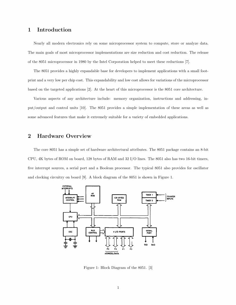
The core 8051 has a simple set of hardware architectural attributes. The 8051 package contains an 8-bit
CPU, 4K bytes of ROM on board, 128 bytes of RAM and 32 I/O lines. The 8051 also has two 16-bit timers,
five interrupt sources, a serial port and a Boolean processor. The typical 8051 also provides for oscillator
and clocking circuitry on board [9]. A block diagram of the 8051 is shown in Figure 1.
Figure 1: Block Diagram of the 8051. [3]
1

2.1 Registers, Ports, Etc.
Figure 2: Full Block Diagram of the 8051. [4]
The full block diagram in Figure 2 shows some of the various registers, ports and other devices on the
8051. The 8051 architecture consists of these features: [5]
• Sixteen-bit program status word (PSW)
• Sixteen-bit program counter (PC) and data pointer (DPTR)
2

• Eight-bit stack pointer (SP)
• Four register banks, each containing eight registers
• Sixteen bytes, which is bit addressable
• Eighty bytes of general-purpose memory for data
• Timer and associated control registers
• Program address register (PAR)
• Instruction register (IR)
• A (the accumulator) and B special registers
• Control registers: TCON, TMOD, SCON, PCON, IP, IE
• Four 8-bit latched ports: P0 - P3
These features combined form the building blocks of the 8051 core architecture. These, and some additional
features will be addressed later.
2.2 Pinout
Figure 3: 8051 DIP Pin Assignments. [4]
3

A pinout of a 40-pin Dual In-Line package is shown in Figure 3. It is important to notice that many of
the pins are used for multiple functions. To reduce the overall pin count of the package, the 8051 multiplexes
pins so that many more functions are available than the number of pins allow. Therefore, not all of the
possible 8051 functions can be used at the same time [5].
2.3 Oscillator and Clocking
Figure 4: 8051 Bus Cycles [3]
The smallest CPU timing unit is the oscillator, called the clock. The 8051 contains circuitry that generates
4

the clock pulses by which all internal operations are synchronized. Pins XTAL1 and XTAL2 are provided
to connect a quartz crystal. Typical crystal frequencies range from 1 megahertz to 16 megahertz. Some
later derivative models operate using faster crystals. This crystal frequency is the basic internal clock of the
microcontroller [5].
Figure 4 shows machine cycle divisions. A machine cycle consists of six states, S1 through S6. Each state
is divided into two phases, P1 and P2. Each phase lasts one clock period. Therefore, one machine cycle lasts
12 clock periods [9].
3 Memory Organization
An operational computer must have memory for program code, usually in ROM, and RAM for variable
data that can be altered as the program executes. The 8051 has internal RAM and ROM for these functions.
Additional external memory can be added if needed by the appropriate circuitry [5].
Figure 5: 8051 Memory Map [3]
5

3.1 Memory Space Separation and Size
Unlike Von Neumann architecture microcontrollers, which use a single address for either program code
or data, but not for both, the 8051 has a Harvard architecture, which uses the same address, in different
sets of memory, for both code and data. The internal circuitry accesses the correct memory set based on the
nature of the operation in progress, as will be discussed later [5].
The 8051 supports 64K bytes of program storage, the lowest 4K being on-chip, the remainder external. In
addition to the 128 bytes of on-chip RAM, the 8051 supports up to 64K of additional external data storage.
The 8051 memory structure is shown in Figure 5 [9].
3.2 Program Storage
After a processor reset, the CPU begins to fetch instructions beginning at address 0000H. This starting
physical address is either on-chip or in external storage depending on the pin designated EA as shown
in Figure 5. If EA is low, the address 0000H and all other program storage address will reference external
storage. If, however, EA is high, addresses 0000H to 0FFFH will reference on-chip ROM and higher addresses
will automatically reference external storage [9].
3.3 Data Storage
Figure 6: 8051 Lower 128-bytes of Internal RAM [3]
The internal data storage of the 8051 consists of the lower 128 byes and the Special Function Register
6

(SFR) space, also 128 byes, which will be discussed later. The lower 128 byes of internal RAM is shown in
Figure 6. The lowest 32 byes, from address 00H to 1FH are grouped into four banks, numbered 0 to 3, of
eight registers each. Only one bank at a time can be in active use, and is selected by a 2-bit field, consisting
of RS0 and RS1 in the Program Status Word (PSW). The eight registers in the active bank are designated
R0 through R7 and can be addressed by name or directly by RAM address. After a reset, the Stack Pointer
(SP), points to the top register of the lowest bank at address 07H.
The 16 bytes above the register banks form a block that can be addressed as either bytes or as 128
individual bits. The byte addresses of this block range from 20H to 2FH. The bit addresses range from 00H
to 7FH. Even though the same numeric address can refer to either a byte of a bit, there is no ambiguity.
Thus, for example, bit address 4F is also bit 7 of byte address 29H. The instruction that uses the address
determines whether the reference is to be a byte or a bit. Addressable bits are useful when a program need
only to remember a binary event [5, 9].
3.4 On-Chip ROM
The block of on-chip ROM occupies code address space 0000H to 0FFFH. The Program Counter (PC)
is used to address program code bytes from addresses 0000H to FFFFH. Addresses referenced higher than
0FFFH will cause the 8051 to fetch code bytes from external program memory. Code bytes can also be
fetched exclusively from external address by grounding the external access pin EA [5].
The contents of the on-chip ROM in the 8051 are masked at the factory. The program designer sends a
program for the 8051 to the chip manufacturer. The manufacturer translates the program into a pattern on
a photographic mask that is used to define a set of interconnections in the silicon during a final step of chip
production. Once this process is completed, the program contained on the chip cannot be changed.
This masking process is highly cost effective for large distributions of chips, such as mass-produced
consumer electronics. To be cost effective, the program must be stable (no changes needed) and completely
bug-free before the masking processes is completed. Some 8051 derivatives allow for program alteration.
Although these options may not be cost effective for mass-production, they do offer a cost and time benefit
for development and small scale productions [9].
7

4 Special Function Registers
Figure 7: Special Faction Map [3]
The 8051 operations that do not use the internal 128-byte RAM address from 00H to 7FH are done by
a group of specific internal register, each called a Special Function Register (SFR), which may be addressed
much like internal RAM, using addresses from 80H to FFH. Some of the SFR locations are bit-addressable
as well as byte-addressable. Figure 7 shows a Special Function Register map. Not all addresses are occupied.
In general, unoccupied addresses are not implemented and reserved for future versions of the 8051 [5, 9].
4.1 Accumulator and B Registers
The 8051 contains 34 general purpose registers. Two of these, the Accumulator (A) and the B register,
hold the results of many instructions. These two registers are known commonly as the CPU registers [5].
When referring to the accumulator as a location in the SFR, ACC is used. Accumulator specific instructions
use the accumulator as A [9]. The accumulator register is the most versatile of the two CPU registers and
is used in many operations including addition, subtraction, integer multiplication and division, and Boolean
bit manipulations. The A register is also used for all data transfers between the 8051 and external memory
8

[5]. Because of this heavy reliance on the accumulator, the 8051 is commonly referred to as having an
accumulator architecture. The B register has a specific function in multiply and divide operations. This
register has no other special function and otherwise may be used as a general memory location [9].
4.2 Program Status Word
Figure 8: Program Status Word Register [3]
Figure 8 shows the flags contained in the Program Status Word Register. Flags are 1-bit registers provided
to store the results of certain program instructions. Other instructions may test the condition of the flags
and make decisions based on the flag status. Many of the more common flags are grouped inside the PSW.
The PSW contains math flags, user program flag F0, and the register select bits that identify which of the
four register banks is currently active. The math flags include Carry (C), Auxiliary Carry (AC), Overflow
(OV), and Parity (P). The user flag F0 may be used for a user-defined purpose. All flags can be set and
cleared directly by the programmer, but are more commonly used as status indicators of instruction results
[5].
Note that although that PSW does not include a zero flag, as many architectures do, this is not a problem
because the 8051 has specific instructions to test the accumulator for zero [9].
9

4.3 Stack Pointer
The stack is an area of RAM that is used with certain instructions to quickly store and retrieve data.
The 8-bit Stack Pointer (SP) register is used to hold a RAM address that points to the top of the stack.
The address in the register points to the RAM address of the last byte of data that was placed on the stack
by a stack operation [5]. Because the stack pointer is 8 bits wide, the maximum stack size is 256 bytes.
The stack pointer is incremented for new data in the stack, so the stack grows upward through memory as
data is stored. On a processor reset, the stack pointer contains the address 07H, causing the stack to start
at location 08H in a register bank. Because programs usually use this area of memory (the registers) for
other uses, the stack pointer can be changed to any internal RAM address by the programmer, causing the
stack to be moved to a different location. The stack is usually moved higher in RAM before doing any stack
operations. Care must be taken when moving the stack to avoid conflicts with other registers, bit-addressable
memory or otherwise reserved areas of RAM [9].
4.4 Program Counter and Data Pointer
The 8051 contains two 16-bit registers: the Program Counter (PC) and the Data Pointer (DPTR). Each
is used to hold the address of a byte in memory. Program instructions are fetched from locations in memory
that are addressed by the program counter. As stated before, code ROM may be fully on-chip, fully off-chip,
or a combination of both. The program counter is automatically incremented after every instruction byte is
fetched and may also be altered by certain instructions such as jumps and branches [5].
The data pointer is a 16-bit quantity held in two 8-bit parts: the high byte in DPH and the low byte in
DPL. The primary purpose of the DPTR is to hold a 16-bit address for certain instructions, especially when
referencing external memory. It can be used as a single 16-bit register or two 8-bit registers [9].
4.5 Port Latches
The 32 I/O pins are organized into four 8-bit ports named P0-P3. Each port has an associated 8-bit
latch, the outputs of which drive the matching I/O pins. The contents of the latches can be read from or
written to in the SFR [9]. Ports will be discussed in more detail later.
10

4.6 Serial Data Buffer
The Serial Data Buffer (SBUF) is actually two different registers sharing a common address. One register
is read-only and the other is write-only. When data are written to SBUF, they go to a transmit buffer and
are held there for serial transmission. When data are read from SBUF, they come from the serial data receive
buffer [9]. Serial communication will be discussed in more detail later.
4.7 Timer Registers
The registers TH0 and TL0 are the high and low bytes, respectively, of the 16-bit counting register for
timer/counter 0. Likewise, TH1 and TL0 are for timer/counter 1 [9]. Some 8051 derivatives include other
timer registers for additional timers to special types of counters. Timers and counters will be discussed in
more detail later.
4.8 Control Registers
The SFR contains registers used for the control and status of the interrupt system, the timers and
counters, and the serial port. The are: Interrupt Priority (IP), Interrupt Enable (IE), Timer Mode (TMOD),
Timer Control (TCON), Serial Port Control (SCON), Power Control (PCON) [9]. Each will be discussed
later.
5 I/O Ports
One of the major features of a microcontroller is the versatility built into the I/O circuits that connect
the microcrontoller to the outside world [8]. To be commercially viable, the 8051 had to incorporate as many
I/O functions as were technically and economically possible [5]. One of the most useful features of the 8051
is four bidirectional I/O ports. Each port has an 8-bit latch in the SFR space as mentioned earlier. To
reduce the overall package pin count, the 8051 employs multiple functions for each port. Each port also has
an output drive and an input buffer. These ports can be used to general purpose I/O, as an address and
data lines, and for certain special functions to be discussed later [9].
11

5.1 Input Loading and Output Driving
Ports 1, 2 and 3 have the equivalent of internal pull-up resistors. When used as input, the pin of P1, P2
and P3 will be high (logical 1) when open-circuited and will source current when pulled low by an external
device. Port 0 does not have the same pull-up feature and is floating (high impedance) when used as an
input. Some care should be taken to avoid confusion when reading a port. Each port has a D-type output
latch for each pin. The SFR for each port is made up of these eight latches, which can be addressed at the
SFR address for the port. The port latches should not be confused with the port pins. A condition can occur
where the port is of such low resistance that the voltage of the pin is at the same level as a low. Reading the
latch would show a 1, but reading the pin would show a 0. Instructions that do read-modify-write operations
read the latch.
When used as outputs, ports 1, 2, and 3 each can drive the equivalent of four LSTTL inputs. Port 0
can drive eight such equivalent inputs. However, manufacturer specification should be carefully followed for
driving. Driving more than two LSTTL inputs typically degrades the noise immunity of the ports. Buffering
the ports when they must drive currents in excess of the manufacturer recommendations may be required.
To speed up 0 to 1 output transitions on ports 1, 2, and 3, an additional pull-up is activated briefly during
output to drive the pin high quickly [5, 9].
5.2 Alternate Port Functions
Pin FunctionP3.0 RXD(serial input port)P3.1 TXD(serial output pin)P3.2 INT0(external interrupt)P3.3 INT1(external interrupt)P3.4 T0(timer/counter 0 external input)P3.5 T1(timer/counter 1 external input)P3.6 WR(external data memory write strobe)P3.7 RD(external data memory read strobe)
Table 1: Alternalte Functions of Port 3 Pins [3]
All of the pins of port 3 have an alternate function, as listed in Table 1. To enable an alternate function,
a 1 must be written to the corresponding bit in the port latch[9]. Unlike ports 1 and 2, which can have
external addressing functions and change all eight port bits when in alternate use, each pin of port 3 may
12

be individually programmed to be used either as I/O or as one of the alternate functions [5].
5.3 Accessing External Memory
Two separate external memory spaces are made available by the 16-bit PC and DPTR and by different
control pins for enabling external ROM and RAM chips. Internal control circuitry accesses the correct
physical memory, depending on the machine cycle state and the instruction being executed.
Because the 8051 has separate program memory and data memory, it uses different hardware signals to
access external storage devices. The Program Store Enable (PSEN) signal is used as the read strobe for
program memory and RD and WR are used as the read and write strobes to access data memory. Note
that RD and WR are alternate functions of P3.6 and P3.7, as mentioned earlier. Ports 0 and 2 are used to
address and access external memory.
Accesses to external program storage always uses a 16-bit address. Accesses to external data storage may
use either an 8-bit or a 16-bit address, depending on the instruction being executed. In the case of a 16-bit
address, the high-order 8 bits of the address are output on port 2, where they are held constant during the
entire memory access cycle. The prior contents of port 2 latched are stored and restored after the memory
cycle has completed.
The low-order 8 bits of the address are multiplexed with the data byte on port 0. That is, it first provides
the lower byte of the 16-bit memory address, then acts as a bidirectional data bus to write or read a byte
of memory data. When used in this mode, port 0 pins are connected to an internal active pull-up; they do
not float as they would normally. The prior contents of port 0 latches are lost. The Address Latch Enable
(ALE) signal must be used to capture the low-order address bits in an external latch [5, 9].
6 Timers and Counters
Many microcontroller applications require the counting of external events, such as frequency of a pulse
train, or the generation of precise internal time delays between actions. Both of these tasks can be accom-
plished using software techniques, but software loops for counting or timing keep the processor occupied so
that other, perhaps more important, functions are not done [6].
13

The 8051 has two 16-bit registers that can be used as either timers or counters. These two up counters
are name T0 and T1 and are provided for general use of the programmer. Each counter may be programmed
to count internal clock pulses, act as a timer, or programmed to count external events as a counter. The
counters are divided into two 8-bit registers called the timer low (TL0, TL1) and timer high (TH0, TH1)
bytes. These registers are in the SFR as pairs of 8-bit registers [5, 9].
6.1 Timing
If a counter is programmed to be a timer, it will count the internal clock frequency of the 8051 oscillator
divided by 12. The register is incremented once per machine cycle, which is equal to once per 12 clock
periods. When used as a counter, the register is incremented on a 1-0 transition (a negative edge) applied
to the appropriate input pin. It takes two complete machine cycles for the 8051 to see the negative edge
transition; the input must be held high for at least one cycle and then low for at least one cycle.
6.2 Timer 0 and Timer 1
Figure 9: Timer/Counter Mode Control Register (TMOD) [3]
The operation mode of timer 0 and timer 1 is determined by the 8 bits written to the TMOD register,
shown in Figure 9. Bits M0 and M1 (one pair for each timer) are used as a two bit field to select one of
14
four operating modes, designated mode 0 through 3. Both counters work the same in modes 0, 1, and 2, but
differently in mode 3 [9].
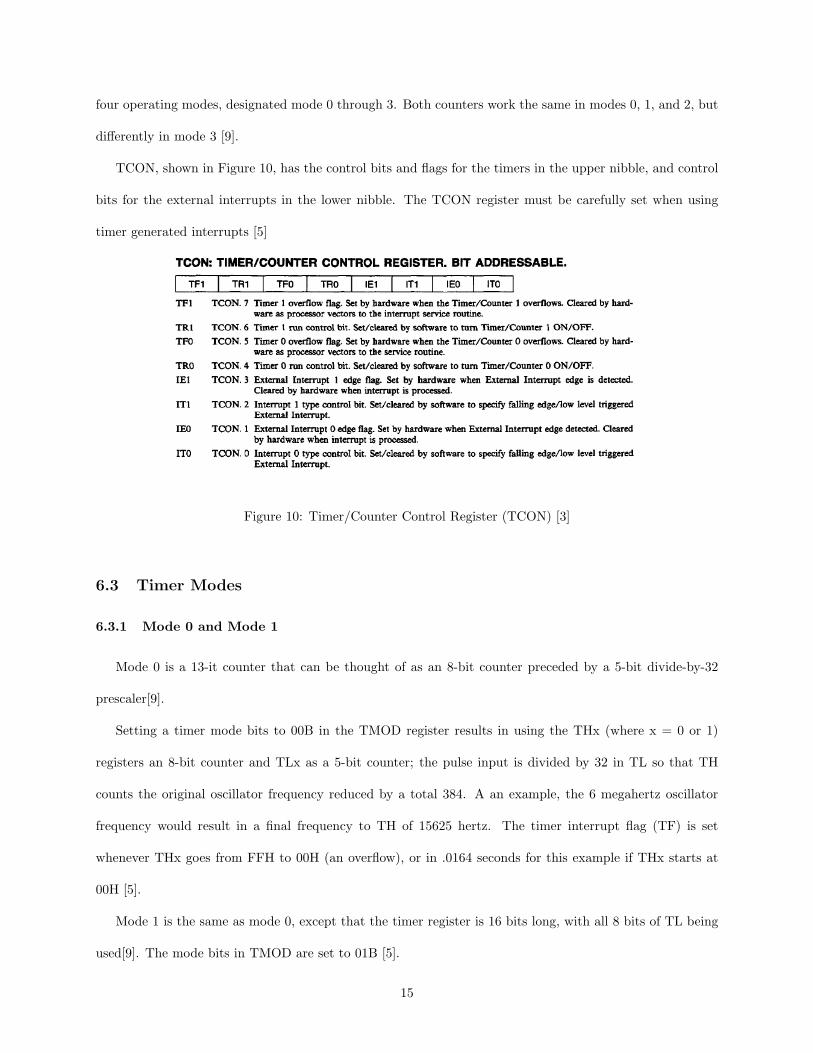
TCON, shown in Figure 10, has the control bits and flags for the timers in the upper nibble, and control
bits for the external interrupts in the lower nibble. The TCON register must be carefully set when using
timer generated interrupts [5]
Figure 10: Timer/Counter Control Register (TCON) [3]
6.3 Timer Modes
6.3.1 Mode 0 and Mode 1
Mode 0 is a 13-it counter that can be thought of as an 8-bit counter preceded by a 5-bit divide-by-32
prescaler[9].
Setting a timer mode bits to 00B in the TMOD register results in using the THx (where x = 0 or 1)
registers an 8-bit counter and TLx as a 5-bit counter; the pulse input is divided by 32 in TL so that TH
counts the original oscillator frequency reduced by a total 384. A an example, the 6 megahertz oscillator
frequency would result in a final frequency to TH of 15625 hertz. The timer interrupt flag (TF) is set
whenever THx goes from FFH to 00H (an overflow), or in .0164 seconds for this example if THx starts at
00H [5].
Mode 1 is the same as mode 0, except that the timer register is 16 bits long, with all 8 bits of TL being
used[9]. The mode bits in TMOD are set to 01B [5].
15
6.3.2 Mode 2
Mode 2 is selected when the mode bits of TMOD are set to 10B. Mode 2 is commonly referred to as an
8-bit auto-reload timer. The TL register is used as an 8-bit stand-alone counter and the TH stores a preset
number. When TL goes from all 1s to all 0s the interrupt flag is set and the contents of TH are transferred
to TL. The contents of TH remain unchanged unless altered by the programmer. Because the contents of
TH are under software control, the counter can be made to divide the count source by any number from 1
to 255 by means of the automatic reload of TH into TL [9].
6.3.3 Mode 3
In mode 3, timer 1 is disabled but holds its current count. Timer 0 mode 3 is split into separate counters.
The first counter is the same as mode 0, except TL0 is used as an 8-bit counter and there is no prescaler
divide. The second counter uses TH0 as an 8-bit counter. The count source is the oscillator divided by 12
and the enable control is the TR1 bit in the TCON register. The first counter sets the TF0 interrupt flag
and the second counter sets TF1. Mode 3 is the only mode in which the timers do not operate independently
[5, 9].
6.4 Timer 2
Timer 2 is a 16-bit timer/counter only in the 8052 family. It is not included in the 8051 core architecture.
The input source for timer 2 can be the clock or an external input. Timer 2 has three operating modes:
capture, auto-load, and baud-rate generator. The input source and mode can be selected by bits in the
T2CON register [9].
7 Serial Ports
In modern multiprocessor distributed systems, computers must be able to communicate with other com-
puters. One cost-effective way to do this is to send and receive data bit serially [5]. The 8051 has a full
duplex serial port that allows for data transmission to be accomplished by hardware while software does
other things. A serial port interrupt is generated by hardware so that the program can read or write serial
16

data to the port at the appropriate time. The receiver hardware is double buffered which allows the receiver
interrupt service to be less-time critical by storing a frame until another frame is received. However, the
first frame must be read before the next frame is received or the first frame will be overwritten and lost.
Both transmit and receive buffers are accessed at the same address in the SFR space. Writing to SBUF
loads the transmit buffer, and reading from SBUF obtains the contents of the receive buffer. The serial port
has four modes of operation to be discussed later [9].
7.1 Serial Port Control and Status Register
Figure 11: Serial Port Control and Status Register (SCON) [3]
SCON, shown in Figure 11, is the serial port control and status register. Bits SM0 and SM1 are used to
select the operating modes for the serial port. The SM2 bit is used in a multiprocessor system where one
8051 acts as a master and send commands to slave devices. These types of systems will not be discussed here.
Note the other bits included in SCON. REN is a software set bit that enables or disables serial reception.
TB8 and RB8 are used in modes 2 and 3 and will be discussed later. TI and RI are transmit and receive
interrupt flags that are set by hardware to trigger a software routine. Both must be cleared in software [5, 9].
17

7.2 Serial Port Modes
7.2.1 Mode 0 - Shift Register Mode
Mode 0 is a half-duplex synchronous operation, also known as shift register mode. Setting bit SM0 and
SM1 in SCON to 00B configured SBUF to receive or transmit data bits using pin RXD for both functions
(but not at the same time). Pin TXD in connected to the internal shift frequency pulse source to supply
shift pulses to external sources. The shift frequency, or baud rate, is fixed at 1/12 of the oscillator frequency,
the same rate used by the timer/counters when operating in the timer configuration. The TXD shift clock
is a square wave that is low to machine cycle states S3-S4-S5 and high for S6-S1-S2 [5].
A shift clock edge will occur during the valid state of each data bit. When transmitting, data are shifted
out of RXD. Received data comes in on pin RXD and should be synchronized with the shift clock produced
at TXD. Note that both RXD and TXD are alternate functions of port 3 pins [9].
Mode 0 is not intended for communication between computers, but as a high-speed serial data-collection
method using discrete logic to achieve high data rates. The baud rate for mode 0 will be much higher than
other modes [5].
7.2.2 Mode 1 - Standard UART
Mode 1 is a full-duplex synchronous operation, also known as a Standard UART. Setting SM0 and SM1
in SCON to 01B, SBUF becomes a 10-bit full-duplex receiver/transmitter that may receive and transmit
data at the same time. Data are sent out RXD and received through TXD. A complete frame consists of a
start bit (always a 0), followed by 8 data bits (LSB first), followed by a stop bit (always a 1). The start and
stop bits are added by the hardware; the software writes the 8-bit data byte to, or reads it from, SBUF.
When transmitting, all 10 bits are sent via TXD. Once all 10 bits have been transmitted, TI is set to
signal software the transmission is complete. When receiving, the start bit is discarded, the stop bit is stored
in RB8 of SCON, and RI is set to indicate a received byte is stored in SBUF. If RI is still set from the
previous receive, indicating that previous byte has not yet been read from SBUF, the new byte will not be
stored and will be lost [5, 9].
Timer 1 is used to generate the baud rate for Mode 1 by using the Overflow flag of the timer. Typically,
18

timer 1 is used in timer mode 2 as an 8-bit auto-reload timer. Care must be taken to ensure the correct
baud rate is being used [5]. Baud rate selection and calculation is beyond the scope of this document. The
reader should consult the Intel MCS-51 Microcontroller Family User’s Manual (see [3]) for this information.
7.2.3 Mode 2 and Mode 3 - Multiprocessor Modes
Mode 2 is similar to mode 1 except 11 bits are transmitted: a start bit, nine data bits, and a stop bit.
The ninth data bit is copied from bit TB8 in SCON during transmit and stored in bit RB8 of SCON when
data is being received. Both start and stop bits are discarded. The 11th data bit is typically used as an
interrupt source to multiprocessor communications.
The baud rate for Mode 2 is either 1/32nd or 1/64th of the oscillator frequency as selected in bit 7
(SCON) of the PCON register. This baud rate is much higher than the standard communication rates. This
high data rate is needed in many multiprocessor application [5, 9].
Mode 3 is the same as mode 2, except the baud rate is variable and can be obtained in the same way as
in mode 1, via timer 1 overflows [9].
7.3 PCON Register
Of the 8 bits in the PCON power control register, only bit 7, SMOD, is used in the standard 8051. As
mentioned earlier, SMOD is used in setting the baud rate of the serial port in mode 2. Other bits are used
in CMOS versions of the 8051 for power-savings modes and general-purpose flags [9].
8 Interrupts
A program only has two ways to determine the conditions that exists in internal and external circuits.
One method uses software processing heavily. Software techniques use up processor time that could be
devoted to other tasks. The second method is to respond to hardware signals, called interrupts, that force
the program to call a special subroutine, called an Interrupt Service Routine (ISR). Interrupts take processor
time only when action by the program is needed. Most applications of microcontrollers involve responding to
events quickly enough to control the environment that generates the events (called real-time programming).
19

Interrupts are often the only way in which real-time programming can be done successfully [5]. The 8051 has
Figure 12: Interrupt Enable Register [3]
five interrupt sources. INT0 and INT1 are external pin interrupt sources. TF0 and TF1 are timer/counter
overflow interrupt flags. Another source comes from the serial port, as discussed earlier. A useful feature of
the 8051 is that the interrupt sources are associated with bit locations in registers. Those bits can be set or
cleared by software, with the same results as when those bits are cleared or set by hardware [5].
As shown in Figure 12, all interrupts or each individual interrupt can be enabled or disabled by setting
or clearing the appropriate bits in the Interrupt Enable (IE) register. If enabled, an interrupt will cause a
call to one of the predefined locations in RAM. The return address automatically is pushed onto the stack
before jumping and is popped back off when an RETI (return from interrupt) instruction is executed. If an
interrupt occurs while it is disabled, or while a higher priority one is running, it becomes pending. As soon
as a pending interrupt is enabled, it will cause a call, unless it was other canceled in software while it was
still pending [9].
8.1 Servicing External Devices
The timing of real-world events is usually asynchronous to the CPU timing; they have no relationship.
In order to monitor and control external devices, a microprocessor must have method of responding to an
event in a timely manner. Interrupts are instrumental in these types of operations [9].
20

8.2 Polling and Buffering
Polling is the method that the processor may use to periodically ask each device if it needs service. The
disadvantage of polling is the amount of CPU time that is dedicated to continually checking all devices.
Polled devices typically buffer, or store, data that it needs to exchange with the processor the next time it is
polled. However, if polling is too slow, and the buffer runs out of data to store, or overflows with too much
data, time will be wasted or data lost. Both conditions are unacceptable in most applications In real-time
programming applications, devices cannot typically wait for a poll from the processor. The device must be
serviced as quickly as possible in order for the application to be useful. A much better way for devices to
signal the processor is using interrupts [9].
8.3 Basic Interrupt Action
I/O devices often require immediate service while the processor is busy doing other things. The interrupt
is a software-controlled hardware feature that forces the processor to stop what it is doing and service the
device that generated the interrupt. When the processor is finished with the device, it may resume the
previous task where it left off. An I/O device will request service by activating an interrupt pin on the CPU.
If the CPU has enabled that interrupt in software, it will initiate its response, often with an acknowledgment
signal sent to the device. This is an example of handshaking between the processor and the I/O device.
The rest of the response is similar to a subroutine call. The CPU will push the return address onto the
stack and branch to a predefined part of memory, where it expects to find the service routine that it must
execute. The last instruction in the routine will be a RETURN, which will pop the return address off the
stack and into the PC register. The CPU will then resume program execution from the point where is was
interrupted [9].
8.4 Multiple Interrupt Sources and Vectoring
It is possible to have multiple interrupt sources. When an interrupt occurs, the processor must first
determine which device caused the interrupt. One method of determining the device that was responsible
is to poll all the devices. However, polling can be time consuming. A faster way is for each device to point
21
to the place in memory where its service routine is stored. The CPU can then go directly to that location.
Such a system is called vectored interrupt.
With a vectored interrupt systems, some problems can arise. What happens if two devices trigger
interrupts at the same time? Which interrupt is serviced first? The 8051 has a priority scheme to solve this
common problem [5, 9].
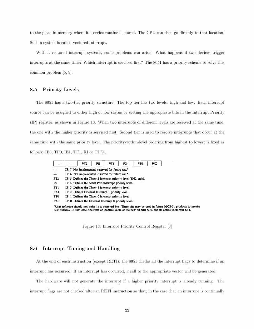
8.5 Priority Levels
The 8051 has a two-tier priority structure. The top tier has two levels: high and low. Each interrupt
source can be assigned to either high or low status by setting the appropriate bits in the Interrupt Priority
(IP) register, as shown in Figure 13. When two interrupts of different levels are received at the same time,
the one with the higher priority is serviced first. Second tier is used to resolve interrupts that occur at the
same time with the same priority level. The priority-within-level ordering from highest to lowest is fixed as
follows: IE0, TF0, IE1, TF1, RI or TI [9].
Figure 13: Interrupt Priority Control Register [3]
8.6 Interrupt Timing and Handling
At the end of each instruction (except RETI), the 8051 checks all the interrupt flags to determine if an
interrupt has occurred. If an interrupt has occurred, a call to the appropriate vector will be generated.
The hardware will not generate the interrupt if a higher priority interrupt is already running. The
interrupt flags are not checked after an RETI instruction so that, in the case that an interrupt is continually
22

being generated, the remainder of the program will still slowly execute.
The time between the activation of the interrupt and the start of execution of the service routine is
referred to as the response time. On the 8051, the best-case response time is three machine cycles and the
worst-case time is nine machine cycles. Response time may be critical in many real time applications [5].
8.7 Activation Levels and Flag Clearing
Interrupts can either be level-triggered or edge-triggered. On the 8051, the external interrupts INT0 and
INT1 can be configured to be either level or edge triggered, depending on the value of the bits IT0 and
IT1 in the TCON register (see Figure 10). The flag bit will be set when the interrupt occurs and cleared
automatically when the call is made to the interrupt vector.
For the timers, the TF0 and TF1 flags are set when the counter overflows from all 1s to all 0s. The
timer interrupts therefor are considered edge triggered. TF0 and TF1 are also cleared automatically during
interrupt service.
The serial port interrupt is generated when either the RI or TI bits are set to 1. RI and TI are not
automatically cleared. The ISR must determine which bit caused the interrupt and clear it as part of the
routine [5].
8.8 Predefined Vector Addresses
The 8051 has predefined vector addresses for interrupts. Table 2 shows this vector. 8051 assemblers will
typically have mnemonics associated with each interrupt source [5].
Interrupt Source Vector AddressIE0 0003HTF0 000BHIE1 0013HTF1 001BH
RI & TI 0023HTF2 & EXF2 002BH
Table 2: Interrupt Vector [3]
23

9 Instructions and Addressing
The 8051 has five addressing modes and five groups of instructions. Different addressing modes allows the
8051 great flexibility and power as a control device [5]. Addressing modes will be discussed, but no examples
will be presented here. It is assumed that the reader is familiar with various addressing modes. The reader
should refer to the Intel MCS-51 Microcontroller Family User’s Manual (see [3]) for more information about
addressing modes.
9.1 Direct Addressing
Direct addressing is the simplest addressing mode of the 8051. Instructions using direct addressing are
2 bytes long. One byte for an 8-bit opcode and one byte for an 8-bit address. The address is a location in
internal RAM or the SFR space. Depending on the type of instruction, the address refers to either a byte
location or a specific bit in a bit-addressable byte.
Figures 6 and 7 showed various address spaces in both RAM and the bit-addressable bytes in the SFR
area. Assemblers for the 8051 usually have predefined mnemonic symbols corresponding to important bit
and byte addresses. Table 3 on Page 25 shows the bit address names, and Table 4 on Page 26 shows the
byte address names. These mnemonics are commonly referenced in 8051 program code [9].
9.2 Indirect Addressing
An instruction using direct addressing specifies the address of the operand explicitly. An instruction
using indirect addressing specifies a register that contains the address of the operand. Because the contents
of the register can be changed by the program, indirect addressing is a powerful technique. Also, most of
the instructions that use indirect addressing are only 1 byte long.
Indirect addressing can access external or internal RAM and addresses can be 8 or 16 bits long. The
8-bit addresses use registers R0-R7. 16-bit addresses use the DTPR register [9].
24

Symbol Bit Position Bit Address MeaningCY PSW.7 D7H Carry FlagAC PSW.6 D6H Auxiliary Carry FlagF0 PSW.5 D5YH Flag 0RS1 PSW.4 D4H Register Bank Select Bit 1RS0 PSW.3 D3H Register Bank Select Bit 0OV PSW.2 D2H Overflow FlagP PSW.0 D0H Parity FlagTF1 TOCN.7 8FH Timer 1 Overflow FlagTR1 TCON.6 8EH Timer 1 Run Control FlagTF0 TCON.5 8DH Timer 0 Overflow FlagTR0 TCON.4 8CH Timer 1 Run Control FlagIE1 TCON.3 8BH Interrupt 1 Edge FlagIT1 TCON.2 8AH Interrupt 1 Type Control BitIE0 TCON.1 89H Interrupt 0 Edge FlagIT0 TCON.0 88H Interrupt 0 Type Control BitSM0 SCON.7 9FH Serial Mode Control Bit 0SM1 SCON.6 9EH Serial Mode Control bit 1SM2 SCON.5 9DH Serial Mode Control Bit 2REN SCON.4 9CH Receiver EnableTB8 SCON.3 9BH Transmit Bit 8RB8 SCON.2 9AH Receive Bit 8TI SCON.1 99H Transmit Interrupt FlagRI SCON.0 98H Receive Interrupt FlagEA IE.7 AFH Enable All InterruptsES IE.4 ACH Enable Serial Port InterruptET1 IE.3 ABH Enable Timer 1 InterruptEX1 IE.2 AAH Enable External Interrupt 1ET0 IE.1 A9H Enable Timer 0 InterruptEX0 IE.0 A8H Enable External Interrupt 0RD P3.7 B7H Read Data for External MemoryWR P3.6 B6H Write Data for External MemoryT1 P3.5 B5H Timer/Counter 1 External FlagT0 P3.4 B4H Timer/Counter 0 External FlagINT1 P3.3 B3H Interrupt 1 Input PinINT0 P3.2 B2H Interrupt 0 Input PinTXD P3.1 B1H Serial Port Transmit PinRXD P3.0 B0H Serial Port Receive PinPS IP.4 BCH Priority of Serial Port InterruptPT1 IP.3 BBH Priority of Timer 1 InterruptPX1 IP.2 BAH Priority of External Interrupt 1PT0 IP.1 B9H Priority of Timer 0 InterruptPX0 IP.0 B8H Priority of External Interrupt 0
Table 3: Predefined bit addresses for 8051 [3, 9]
25

Symbol Hex Address MeaningACC E0 AccumulatorB F0 Multiplication RegisterDPH 83 Data Pointer (high byte)DPL 82 Data Pointer (low byte)IE A8 Interrupt EnableIP B8 Interrupt PriorityP0 80 Port 0P1 90 Port 1P2 A0 Port 2P3 B0 Port 3PSW D0 Program Status WordSBUF 99 Serial Port BufferSCON 98 Serial Port ControllerSP 81 Stack PointerTCON 88 Timer ControlTH0 8C Timer 0 (high byte)TH1 8D Timer 1 (high byte)TL0 8A Timer 0 (low byte)TL1 8B Timer 1 (low byte)TMOD 89 Timer Mode
Table 4: Predefined data addresses for 8051 [3, 9]
9.3 Register Addressing
Register instructions use the contents of one of the registers, typically R0-R7, as the operand. All
register instructions are 1 byte long. A few register instructions are register-specific; they do not allow
the programmer to specify an arbitrary register. Register instructions rely on the accumulator as a second
operand if needed [9].
9.4 Immediate Operand Instructions
Instructions that use immediate operands have a numeric constant following the op-code. The constants
can be 8 or 16 bits long, depending on the instruction [9]. Immediate operand instructions are useful in
loading specific numerical values into registers.
9.5 Indexed Addressing
The 8051 has two different uses for indexed addressing: reading data tables from program memory space
and implementing jump tables. In either case, a 16-bit register holds a base address and the accumulator
holds an 8-bit displacement or index. The address of the data byte (or jump address) is the sum of the
26

16-bit base address and the 8-bit displacement held in the accumulator. Because the addition is unsigned,
the result is always a forward reference from the base address of 0 to 255 bytes. The base register is either
DPTR or the PC [9].
10 Instruction Groups
The 8051 has 111 instruction types. Counting the variations of these types, there are 255 different
instructions. Each hex code from 00H to FFH corresponds to a valid instruction, except A5 which is reserved
for future use. The instructions fall into five general groups: arithmetic, logic, data transfer, Boolean, and
branching [9]. A brief description of each group, and some specific instructions follows. However, the reader
should consult the Intel MCS-51 Microcontroller Family User’s Manual (see [3]) for a complete listing of
instructions and detailed descriptions.
10.1 Arithmetic Operations
The 8051 has the typical arithmetic operations of an 8-bit processor: add (ADD), add-with-carry
(ADDC), subtract-with-borrow (SUBB), increment (INC), decrement (DEC), and decimal-adjust-accumulator
(DA). It also has two advanced operations not as typical of 8-bit microprocessors: multiply (MUL) and divide
(DIV) [8, 9].
MUL AB multiplies the contents of the accumulator by the contents of the B register as unsigned 8-bit
integers to give a 16-bit result. The lower order 8 bits of the result are stored in the accumulator and the
higher-order bits will be in the B register. DIV AB causes the contents of the accumulator to be divided
by the contents of the B register as unsigned integer numbers. The integer part of the result will be in the
accumulator, and the remainder will be stored in the B register.
10.2 Logic Operations
Logic operations of the 8051 include and (ANL), or (ORL), exclusive-or (XRL), clear and complement
(CLR and CPL), and rotates (RL, RLC, RR, RRC). Also in the group is the SWAP A instruction which
swaps nibbles within the accumulator. SWAP is useful when working with 4-bit quantities such as BCD
27

numbers [9].
10.3 Data Transfer Operations
The basic data transfer instruction is move, which has three forms: MOV, MOVC, and MOVX. Also
included in the group are PUSH, POP and XCH(exchange).
MOV instructions are used to reference internal RAM and SFR space. Two MOVC instructions are used
to move bytes from program memory into the accumulator, as from a data table. The MOVX instructions
are used to reference external RAM [9].
10.4 Boolean Operations
This group of instruction is associated with the single-bit Boolean processor hardware of the 8051. This
group include set and clear, and, or and complement instructions. Bit-level move instructions and bit-level
test conditional jumps. This group makes up a miniature assembly language set for the Boolean processor
which will be discussed shortly [9].
10.5 Branching Operations
Included in this group are all subroutine calls and returns and various conditional and unconditional
jumps. The conditional jumps are relative to the first byte of the next instruction. Because the jump is
given as a signed two’s complement 8-bit number, the range is -128 to +127 bytes, allowing for forward and
backward jumps.
The jump instruction has three basic versions: short (SJMP), long (LJMP), and absolute (AJMP).
The short jump uses a relative offset as described above. The long jump uses a 16-bit address as part of
the instruction which allows a jump to any reference in the 64K program memory space. The long jump
instruction is 3 bytes long. The absolute jump uses an 11-bit address which is split into 8 lower bits and
5 upper bits. The 3 upper bits are combined with a 5-bit operation specifier to make an 8-bit opcode.
Therefore, the entire instruction is only 2 bytes long. The 11 bits of the address are substituted for the lower
11 bites in the program counter, which means that the location referenced must be within 2K bytes of the
28

instruction following the absolute jump. The upper 5 bits in the PC remain the same [9].
11 Boolean Processor
The single bit Boolean processor can thought of as a built-in bit-level coprocessor which uses the Boolean
set of operations as discussed earlier. The Boolean processor is not a true coprocessor because it does not
run separately. All of the port lines, 128 bits in RAM and many bits in the SFR space register have bit
addresses and are capable of bit-level access. this type of hardware and software combination makes the
8051 well suited for control application that have many on/off kinds of inputs and outputs such as switches,
lights, relays and stepper motor drivers [9].
11.1 Carry
The carry bit, bit 7 of the PSW, is the equivalent of an accumulator for the Boolean processor. the
name CY is used to designate the carry bit then referring to it as a bit address and the symbol C is used
in register-specific instructions that reference the carry bit. The assembler will translate the symbol CY to
the number D7H, the bit address of the carry bit. Thus, the instructions CLR PSW.7 and CLR CY are
equivalent.
Bits from the SFR space registers, from internal RAM, and from I/O ports can be read into CY. Opera-
tions such as AND and OR can be performed on CY and the result written back to a bit address. Program
branching can be conditional on the state of CY or any other addressable bit. Extensive bit manipulation
can be done without having to use extraneous code to mask off bits to extract them from bytes [9].
29
List of Tables
1 Alternalte Functions of Port 3 Pins [3] . . . . . . . . . . . . . . . . . . . . . . . . . . . . . . . 12
2 Interrupt Vector [3] . . . . . . . . . . . . . . . . . . . . . . . . . . . . . . . . . . . . . . . . . . 23
3 Predefined bit addresses for 8051 [3, 9] . . . . . . . . . . . . . . . . . . . . . . . . . . . . . . . 25
4 Predefined data addresses for 8051 [3, 9] . . . . . . . . . . . . . . . . . . . . . . . . . . . . . . 26
List of Figures
1 Block Diagram of the 8051. [3] . . . . . . . . . . . . . . . . . . . . . . . . . . . . . . . . . . . 1
2 Full Block Diagram of the 8051. [4] . . . . . . . . . . . . . . . . . . . . . . . . . . . . . . . . . 2
3 8051 DIP Pin Assignments. [4] . . . . . . . . . . . . . . . . . . . . . . . . . . . . . . . . . . . 3
4 8051 Bus Cycles [3] . . . . . . . . . . . . . . . . . . . . . . . . . . . . . . . . . . . . . . . . . . 4
5 8051 Memory Map [3] . . . . . . . . . . . . . . . . . . . . . . . . . . . . . . . . . . . . . . . . 5
6 8051 Lower 128-bytes of Internal RAM [3] . . . . . . . . . . . . . . . . . . . . . . . . . . . . . 6
7 Special Faction Map [3] . . . . . . . . . . . . . . . . . . . . . . . . . . . . . . . . . . . . . . . 8
8 Program Status Word Register [3] . . . . . . . . . . . . . . . . . . . . . . . . . . . . . . . . . 9
9 Timer/Counter Mode Control Register (TMOD) [3] . . . . . . . . . . . . . . . . . . . . . . . 14
10 Timer/Counter Control Register (TCON) [3] . . . . . . . . . . . . . . . . . . . . . . . . . . . 15
11 Serial Port Control and Status Register (SCON) [3] . . . . . . . . . . . . . . . . . . . . . . . . 17
12 Interrupt Enable Register [3] . . . . . . . . . . . . . . . . . . . . . . . . . . . . . . . . . . . . 20
13 Interrupt Priority Control Register [3] . . . . . . . . . . . . . . . . . . . . . . . . . . . . . . . 22

References
[1] Basic Introduction to the 8051 Microcontroller. University of California Dept. of Computer Science.
http://www.cs.ucr.edu/ dalton/i8051/.
[2] Intel MCS-51. CPUShack.net. http://www.cpushack.net/IntelMicrocontrollers.html.
[3] MCS-51 Microcontroller Family User’s Manual. Intel Corporation, 1980. Datasheet.
[4] 8-bit Microcontroller with 4K Bytes Flash - AT89C51. Atmel Corporation, 2000.
[5] K.J. Ayala. The 8051 Microcontroller - Architecture, Programming, and Appications. West, Minneapolis,
2nd edition, 1997. pg 55 - 86.
[6] C.H. Chen. Computer Engineering Handbook. McGraw-Hill, New York, 1992.
[7] M.F. Hordeski. The Illustrated Dictionary of Microcomputers. TAB, Blue Ridge Summit, PA, 3rd
edition, 1990.
[8] M. Rafiquzzaman. Microcomputer Theory and Applicaitons. Wiley, New York, 2nd edition, 1987.
[9] J.W. Steward and K.X. Miao. The 8051 Microcontroller - Hardware, Software and Inerfacing. Prentice
Hall, New Jersey, 2nd edition, 1999. pg 19 - 46.
[10] Stallings W. Computer Organization and Architecture - Designing for Performance. Prentice Hall, 7th
edition, 2006.