copyright warning &...
TRANSCRIPT

Copyright Warning & Restrictions
The copyright law of the United States (Title 17, United States Code) governs the making of photocopies or other
reproductions of copyrighted material.
Under certain conditions specified in the law, libraries and archives are authorized to furnish a photocopy or other
reproduction. One of these specified conditions is that the photocopy or reproduction is not to be “used for any
purpose other than private study, scholarship, or research.” If a, user makes a request for, or later uses, a photocopy or reproduction for purposes in excess of “fair use” that user
may be liable for copyright infringement,
This institution reserves the right to refuse to accept a copying order if, in its judgment, fulfillment of the order
would involve violation of copyright law.
Please Note: The author retains the copyright while the New Jersey Institute of Technology reserves the right to
distribute this thesis or dissertation
Printing note: If you do not wish to print this page, then select “Pages from: first page # to: last page #” on the print dialog screen

The Van Houten library has removed some ofthe personal information and all signatures fromthe approval page and biographical sketches oftheses and dissertations in order to protect theidentity of NJIT graduates and faculty.

ABSTRACT •
PLASMA INDUCED DAMAGE TO SiAND SiGe DEVICES AND MATERIALS
byWei Zhong
This thesis studied the plasma-induced damage to Si and strained Sii_„Ge,,, and the
resulting change in device characteristics. The energetic particles (ions, electrons and
photons) in plasma reactor present a potentially hostile environment for processing VLSI
devices. An inductively coupled plasma (ICP) reactor was used to study its damage
effects to thin gate oxides. Electrical characterizations by C-V, ramped voltage
breakdown (RVB) and deep-level transient spectroscopy (DLTS) measurement, and x-ray
photoelectron spectroscopy (XPS) analysis were employed to investigate the damages to
thin gate oxides and Si/Si0 2 interface. The shift of flat band voltage, the reduction of
breakdown voltage and the creation of high interface trap density were found to be in
good agreement with the creation of suboxidation states at Si/Si02 interface. It is
observed that device damage is well associated with the reactor operating conditions. The
major mechanism responsible for damage appeared to be high-energy electron charging
which occurred when only the ICP power was activated, without any rf bias to the wafer-
carrying electrode. Energetic particle bombardment damage was dominant when the
wafer-carrying electrode' was biased and the damage was considerably higher for rf bias
power grater than 35W.
The effect of plasma processing to the strained Sii_„Ge x layer of p+- n diode has
been investigated. The effect of SFr plasma, used to etch an overlying Si film stopping at
the strained Sii_„Ge x film, on the electrical properties of an underlying Sii_ xGex/Si
heterojunction device was studied. The changes of C-V and I-V characteristics, such as
higher depletion capacitance and lower diffusion current were attributed to ion
bombardment and radiation-induced bonding change, such as creation of interface charges
and recombination centers. The TEM analysis revealed the dislocation loops in Si/Sii-xGex
/Si outside the aluminum contact region due to the ion bombardment stress. The 02
plasma asking has moderate effect to Sii_„Ge x device when the device was protected by
aluminum contact layer.
The C-V profiling techniques on SiGe MOS structures were used to investigate
the change of valence band discontinuity (dEv) at the Si/SiGe interface before and after
plasma exposure and high temperature annealing. Wet and plasma etched samples were
annealed at 500, 600, 700 and 800 °C for 60 seconds. It was observed that the accuracy of
extracting the changes of dEv using the C-V profiling was strongly influenced by the
release of electrons from the traps at Si02/Si interface, which were created during the
low-pressure CVD Si02 deposition. The device simulations have been used to confirm
this finding. By carefully analyzing the C-V profile at slight depletion region the band
gap modifications at back Si/SiGe interface due to process-induced damage could be
evaluated. The dry etched sample was partially relaxed after 700 °C annealing while wet
etched sample was partially relaxed after 800 °C annealing. Dry etched sample
demonstrated a faster relaxation mechanism as compared to its wet etched counterpart
due to the creation of dislocation loops by dry etching process. The C-V method is a
simple, fast and efficient approach to estimate any band-gap modification in SiGe due to
process-induced damage, but the measurements and simulations in slight depletion region
should be carried out with special care and high resolution.

PLASMA INDUCED DAMAGE TO SiAND SiGe DEVICES AND MATERIALS
byWei Zhong
A DissertationSubmitted to the Faculty of
New Jersey Institute of TechnologyIn Partial Fulfillment of the Requirements for the Degree of
Doctor of Philosophy in Electrical Engineering
Department of Electrical & Computer Engineering
May 2001

Copyright © 2001 by Wei Zhong
ALL RIGHTS RESEARVED

APPROVAL PAGE
PLASMA INDUCED DAMAGE TO SiAND SiGe DEVICES AND MATERIALS
Wei Zhong
Dr. D. Misra, Dissertation Advisor (Date)Associate Professor of Electrical and Computer Engineering, NJIT
Dr. M. osnowski, Committee Member (Date)Associate Professor of Electrical and Computer Engineering, NJIT
Dry. Comely, Committee *Aber (Date)Professor of Electrical and Computer Engineering, NJIT
Dr. K. Sc6i,-Committee Member (Date)Professor of,,E and Computer Engineering, NJIT
Dr. P. K. Swain, Committee Member (Date)Technology Leader, Sarnoff Corporation

BIOGRAPHIC SKETCH
Author: Wei Zhong
Degree: Doctor of Philosophy in Electrical Engineering
Date: May 2001
Undergraduate and Graduate Education:
• Doctor of Philosophy in Electrical EngineeringNew Jersey Institute of Technology, Newark, NJ, 2001
• Master of Science in Electrical EngineeringNew Jersey Institute of Technology, Newark, NJ, 1992
• Bachelor of Science in Electronics EngineeringSudan University, Shanghai, P. R. China, 1985
Major: Electrical Engineering
Presentations and Publications:
D. Misra, W. Zhong, B. Bartynski, V. Patel and B. Singh,"Etch Induced Damage in High Density Inductively Coupled Plasma EtchingReactor," Semiconductor Science and Technology, Vol. 11, No. 5, p. 816-821,May 1996.
W. Zhong, D. Misra, B. Bartynski, V. Patel and B. Singh,"Etch Induced Damage in High Density Inductively Coupled Plasma EtchingReactor", Proceeding of the Tenth Symposium on Plasma Processing, G. S.Mathad and D. W. Hess, Editor, Electrochemical Society Proceeding, Vol. PV-94-20, p. 120-131, 1994.
W. Zhong, D. Misra, J. Gaudani, M. W. Cole, T. P. Monaha and R. T. Lareau,"Electrical studies on SFr and 02 plasma etched SiGe/Si p +-n heterojunction,"Proceedings of the Symposium on the degradation of electronic device due todevice operation as well as crystalline and process-induced defects, p. 149 - 156,1994.
W. Zhong, D. Misra, H. Amin,"Electrical studies on SFr and 02 plasma etched SiGe/Si p -n heterojunction,"
iv
Electrochemical Society Interface, Vol. 2, No. 3, p. 122, 1993.
W. Zhong and D. Misra,"Reactive Ion Etching Damage to Strained SiGe Heterojunction Diode,"Proceedings of the 23 rd European solid State Device Research Conference,Grenoble, France, p321-324, September 13-16, 1993.
W. Zhong, H. Amin, J. Gaudani and D. Misra,"Damage to SiGe strained layers due to reactive ion etching,"The Microelectronic Processing '93, SPICE Symposium Monterey, California,September 27-29, 1993.

This thesis is dedicated to my wife Hong, daughter Teresaand my parents Yikuang & Wenying.
vi

ACKNOWLEDGEMENT
First and foremost, thanks to Prof. D. Miser, who not only served as my research
advisor, providing valuable and countless resources, insights, and intuitions, but also
constantly gave me encouragement, supports and assurances.
Special thanks are due to Dr. M. Sosnowski, Dr. R. Comely, Dr. P. K. Swain, Dr.
K. Sohn for actively participating in my committee. Sinancial support from National
Science Foundation (grant No. ECS-9207665) is acknowledged.
My wife, Hong, provided me continuous care, love and understanding. My
daughter, Teresa, brought me everlasting smiles and joys.
Thanks to the Hashimoto Awards committee to select this research work for the
Annual Hashimoto Award.
vii

TABLE OF CONTENTS
Chapter Page
1 INTRODUCTION 1
1.1 Motivation 1
1.2 Objectives of the Research 3
1.3 Thesis Organization 5
2 PLASMA ETCHING PROCESS AND PLASMA DAMAGE 7
2.1 Basic Physical Phenomena in RS Discharges 7
2.2 General Description of Plasma Etch Tools 12
2.3 Plasma Induced Damage to Silicon Devices 17
2.3.1 Plasma Damage to Si/SiO2 System 17
2.4 Plasma Damage to Si/Sii_,,Gre„ Heterojunction Systems 20
2.4.1 Sii_„Ge„ Material and Devices 20
2.4.2 Physical and Electrical Damage to Strained Sii,Ge x Devices.. 26
3 EXPERIMENTAL TECHNIQUES 27
3.1 Electrical Characterization 27
3.1.1 I-V & C-V Measurements to Evaluate MOS System 27
3.2 Deep Level Transient Spectroscopy (DLTS) Techniques 33
3.3 Physical Characterization 41
3.3.1 Secondary Ion Mass Spectroscopy (SIMS) 41
3.3.2 X-Ray Photoelectron Spectroscopy (XPS) 42
3.3.3 Transmission Electron Microscopy (TEM) 44
3.4 Simulation of Sii_,,Gex Device for Damage Estimation 46
3.4.1 Overview of Device Simulator 46
viii

TABLE OF CONTENTS(Continued)
Chapter Page
3.4.2 Important Physics and Equations in SiGe MOS Simulation .. 47
3.4.3 Simulation of Sii_„Ge,, MOS Capacitor 50
4 ETCH-INDUCED DAMAGE TO MOS DEVICE IN HIGH-DENSITY ICPETCHING REACTOR 55
4.1 Introduction 55
4.2 Experimental Details 56
4.3 Measurement Results 60
4.3.1 C-V Measurements 60
4.3.2 Breakdown Measurements , 64
4.3.3 DLTS Analysis 65
4.3.4 XPS Characterization 67
4.4 Discussion of Results 70
4.5 Summary 71
5 PLASMA INDUCED DAMAGE TO STRAINED Sii_xGe„ 72
5.1 Electrical Studies on SF6 and 02 Plasma Etched Sii_,,Ge x p-nHeterojunction 72
5.1.1 Sample Preparation 73
5.1.2 Current-Voltage Measurements 76
5.1.3 C-V Measurements 77
5.1.4 TEM Analysis 77
5.1.5 Effects of 02 Plasma Ash Process 78
ix

TABLE OF CONTENTS(Continued) •
Chapter Page
5.1.6 Summary 79
5.2 Evaluation of Plasma Process-Induced Bandgap Modification ofStrained Sii_xGe,, Heterojunction Using MOS Capacitor 80
5.1.1 Sample Preparation 80
5.1.2 C-V Measurements 82
5.1.3 Device Simulation 84
5.1.4 Discussion of Results 95
5.1.5 Summary 97
6 CONCLUSIONS 98
6.1 Suggestions for Suture Work 100
APPENDIX EXAMPLE OS ATLAS INPUT SILE 101
REFERENCES 103

LIST OF TABLES
Table Page
4.1 A list of the various processing conditions 57
5.1 List of simulated SiGe MOS structures 85
xi

LIST OF FIGURES
Figure Page
2.1 Schematic view of a dc glow discharge showing the most prominentregions of the discharge 8
2.2 Schematic view of rf discharge 10
2.3 Schematic diagram of (a) diode and (b) triode reactor configurations 13
2.4 Basic steps in a dry-etching processing 15
2.5 Illustration of an inductively coupled plasma reactor 16
2.6 Energy band diagram for thermal Si02 layer on an underlying Si substrateexposed to low-energy ions and photos which are present in an RIE 18
2.7 Idealized model for the space-charge build-up as a function of time duringIrradiation of a MOS structure under a positive gate bias 19
2.8 Energy bandgap versus lattice constant 20
2.9 Strained and unstrained SiGe layer 21
2.10 Critical thickness versus Ge content 22
2.11 Energy band diagram of graded-base SiGe HBT compared to a Si BJT.. ..... 24
2.12 (a) A fully pseudomorphic pMOS layer configuration with typical designparameter. (b) The quantum well for holes and inversion of the n- SiGelayer under a sufficiently high negative gate voltage 24
3.1 To illustrate the operation of an MOS capacitor, capacitance as a functionof bias, and the corresponding energy-band diagrams are shown inaccumulation, depletion, inversion, and at Hatband 29
3.2 Normalized high frequency and low frequency capacitance as a functionof gate bias calculated for and acceptor concentration of 2x10 1r
CM-3
,
oxide thickness 100nm, and T=300 K 30
3.3 (a) Low frequency equivalent circuit of MOS, (b) high frequency equivalentcircuit of MOS 31
3.4 Combined (a) high frequency (1MHz) and (b) low frequency C-V curves fora MOS capacitor 32
ii

LIST OF FIGURES(Continued)
Figure Page
3.5 Typical time dependence involved in pulsed bias capacitance transients formajority- and minority carrier traps 35
3.6 Injection pulse sequence which is used to produce a capacitance transient fora minority-carrier trap 36
3.7 Majority-carrier pulse sequence which is used to produce a capacitancetransient for a majority-carrier traps 36
3.8 Illustration of how a double boxcar is used to define the rate window 38
3.9 Thermal emission rates vs 1000/T determined from the DLTS spectra 39
3.10 Schematic diagram of a secondary ion mass spectrometer 41
3.11 SiGe MOS capacitor structure used for simulation 51
3.12 Simulated device structure with mesh 51
3.13 Atlas command group with primary statements in each group 52
3.14 Use Tonyplot to display the C-V plot 53
3.15 Use Tonyplot to display the energy diagram cross the MOS capacitor undercertain bias condition 54
4.1 A schematic diagram of the ICP reactor 57
4.2 Normalized C-V characteristics of various samples: (a) immediately aftermetal deposition; (b) after a 10 minutes annealing at 280°C in N2 ambient 62
4.3 Quasi-static C-V curves for MOS capacitors after plasma etching in an ICPreactor with different process conditions 63
4.4 The breakdown distribution of various samples 64
4.5 DLTS spectra for the control sample #1 and the plasma etched sample #4 66
4.6 Interface traps density N„ in the plasma etched sample (#4) as a function ofenergy 66
4.7 XPS spectra of various samples 68

LIST OF FIGURES(Continued)
Figure Page
4.8 XPS counts for various suboxide states 69
5.1 Scanning electron microgragh of the RTCVD wafer 72
5.2 SIMS profiles for as-grown RTCVD sample 74
5.4 Wet etching results 74
5.4 Device structures were used for study and comparison 75
5.5 The I-V characteristics of wet etched sample #1 and SS6 plasma etchedsample #2 76
5.6 The C-V characteristics of wet etched sample and SSr plasma etched sample.. 77
5.7 (a) High resolution TEM of Si/ Sii_xGex /Si interface after plasma(b) Weak beam dark field TEM microgragh showing the dislocation loops..... 78
5.8 The I-V characteristics of unetched sample#4 and 02 plasma ashed sample. 79
5.9 Typical structure of MOS capacitor used in this study 80
5.10 Schematic band diagram under the slight depletion condition (a)
and the accumulation condition (b) 81
5.11 Typical C-V profiles obtained for the wet etched samples 84
5.12 Typical C-V profiles obtained for the dry etched samples 84
5.14 Simulated C-V plots of SiGe MOS capacitors with different energybandgap values 87
5.14 Energy band diagram in G1 and G2 under —0.5V bias 88
5.15 Hole concentration in G1 and G2 under —0.5V bias 89
5.16 Energy band diagram in 01 and G2 under —1.25V bias 89
5.17 Hole concentration in G1 and G2 under —0.5V bias 90
Div

LIST OF FIGURES(Continued)
Figure Page
5.18 Simulated C-V plots of SiGe MOS capacitor with Si02 fixed positive charges 91
5.19 Simulated C-V plots of SiGe MOS capacitor with Si0 2 interface traps(with different trap densities and different trap energy levels) 93
5.20 Simulated C-V plots of SiGe MOS capacitor with Si02 fixed positive chargesand interface traps to match Figure 5.11 94
5.21 Simulated C-V plots of Sii,Gex MOS capacitor with additional relaxedstructures (G9', G10', G11' and G12') for comparison 94
5.22 Zoomed plot of Figure 2.1 at slight depletion region 96
Dv

CHAPTER 1
INTRODUCTION
1.1 Motivation
This is a silicon world. Greater than 95% of today's $200 billion plus global
semiconductor market uses the semiconductor silicon (Si) to realize a host of integrated
circuits (IC) ranging from 1 GHz microprocessors to 64 Mb dynamic random-access
memory (DRAM) chips. Si has a number of practical advantages over the other numerous
semiconductors, including: 1) an extremely high-quality dielectric (Si02) can be easily
grown on Si and used for isolation, passivation, or as an active layer (e.g., gate oxide); 2)
Si can be grown in very large, virtually defect-free single crystal (200 mm in production
today, rapidly moving to 400 mm), yielding many (low-cost) IC's per wafer; 4) Si has
excellent thermal properties allowing for the efficient removal of dissipated heat; 4) Si
can be controllably doped with both n- and p=type impurities with extremely high
dynamic range (10 12=1022 cm3 ); 5) Si has excellent mechanical strength, facilitating ease
of handling and fabrication; 6) it is easy to make very low-resistance ohmic contacts to
Si, thus minimizing device parasitics; and 7) Si is extremely abundant and easily purified.
Thus, from IC manufacturing standpoint, Si is a dream come true.
Introducing Ge into Si has a number of consequences. First and most importantly,
because Ge has a larger lattice constant than Si, the energy bandgap of Ge is smaller than
that of Si (0.66 eV versus 1.12 eV), thus Si i _„Ge,, has a bandgap smaller than that of Si,
making it a suitable candidate for bandgap engineering in Si. In addition, the compressive
strain lifts the conduction and valence band degeneracies at the band extremes,
effectively reducing the density of states and improving the carrier mobility with respect
1

2
to pure Si (the latter due to a reduction in carrier scattering). The Sii,,Ge x heterojunction
combines heterojunction device performance with silicon manufacturability. It has been
the subject of many investigations in recent years.
A series of Si-compatible hetero-structure devices, based on epitaxial growth in
the Si/Sii_xGex system, has stirred a strong interest for high-speed devices. The narrow
band gap of strained Sii,Gex has been used to fabricate heterojunction bipolar transistors
(HBT's) [1, 2], modulation-doped field effect transistors (MODSET' s) [4], long
wavelength optoelectronics devices [4, 5], and tunneling and superlattice devices. Due to
the lattice mismatch between silicon and germanium, the Sii,Ge x film gown on silicon is
strained up to a critical thickness. It is very important to preserve the quality of these
heterojunctions throughout the fabrication process.
Dry etching techniques such as reactive ion etching (ERIE), magnetron reactive ion
etching (MRIE), plasma etching (PE), ion beam etching (IBE), electron cyclotron
resonance (ECR) etching, reactive ion beam etching (RIBE) and inductively coupled
plasma (ICP) etching can cause damage and contamination effects in exposed materials
[6-18]. In fact, damage is often inherent in these processes due to the presence of ion
bombardment, which can create bonding damage in semiconductors and insulators [6=14,
16, 18], as well as due to the presence of UV radiation, which can create bonding damage
in insulators [15]. Contamination is also often inherent in these processes due to the
presence of residue layers made up of reactant species and reaction products and due to
the presence of impurities which may permeate the etched material during the dry etching
exposure [8, 9, 16-22]. Inductively coupled plasma sources have emerged as the most
used in plasma etchers. They are capable of uniform etching of anisotropic features over
3
large area wafers at etch rates comparable to conventional high-pressure capacitively
coupled reactive ion etching tools. The ion energies incident on the wafers can be
effectively decoupled from plasma generation by independently applying rf power to the
wafer chuck.
The reliability and electrical performance of these Si devices and strained Si/Sii_xGex
hetero-structure devices may be significantly affected by plasma processing during
device manufacturing. Creation of strain-relieving misfit dislocation and/or threading
dislocations [24] may be possible when strained Si i ,Gex films are processed using
reactive ion etching. Though reactive ion etching of Si has been studied the impact of
inductively coupled plasma on Si device are still unfolding. Besides not much is known
about the modifications to electrical characteristics of strained Si l _„Gex . It is very
important to show that how the plasma process affects the strained Sii,Ge x hetero-
structure material and devices.
1.2 Objectives of the Research
The overall goal of the research carried out for this thesis has been to obtain a basic
understanding of plasma induced electrical and physical damages to Si and SiGe devices
leading to the optimization of plasma etch process and development of next generation
plasma etch tools suitable for sub-micro heterojunction devices. The investigation has
been focused on studying the issues related to device physics with the objective of
gaining a fundamental understanding of the damage mechanisms of the associated plasma
etching.

4
This broad objective of this program has been achieved by carrying out research
in two key areas. Sirstly, by using well known Si MOS device to evaluate the plasma
induced damage in advanced ICP reactor; and secondly by applying the similar testing
techniques and the device simulations to SiGe p +-n diode and SiGe MOS devices.
Electrical and physical characterizations, such as I-V, C-V, Deep Level Transient
Spectroscopy (DLTS), Transmission Electron Microscopy (TEM), X-Ray Photoelectron
Spectroscopy (XPS), were used to study the plasma induced damages in ICP reactor.
These studies were aimed at establishing the correlation between and electrical and
physical damage, and developing basic understanding of damage mechanisms.
C-V profiling on Sil_„Gex MOS capacitor is potentially powerful method to
estimate plasma process-induced band-gap modifications. The presence of interface trap
has significantly influenced the measurement result. In this thesis, the utility of device
simulator is demonstrated by the insights gained into the underlying mechanisms of space
charge and surface-state charge between heterojunction semiconductor and insulator. The
finding of the influence of interface traps has been simulated and it correlates with the
measurement result well.
The results of this work have significant technological consequences and
applications. Sor example, the fundamental understanding of etch induced damage to thin
gate oxide in ICP reactors will enable their widespread usage by integrated circuit
manufactures. In addition, the testing and simulation results of Sii_„Gre„ device in this
thesis will help to develop new methods of detection and approaches of damage control
of plasma induced damage in Sii_„Ge x materials and devices.

5
1.3 Thesis Organization
Chapter 2 reviews basic physic phenomena in RS glow discharges, plasma etching tools,
and the fundamental understanding of plasma induced damage to Si and SiGe devices.
The background of SiGe technology is also described in that chapter.
Chapter 3 describes electrical and physical measurement techniques that have
been used for this research. That includes I-V, C-V, DLTS developed as a part of this
thesis work, SIMS, XPS and TEM. The knowledge of these techniques will lead to
understand and interpret the research results in this thesis. In addition an overview of
device simulation relevant to this work is presented in that chapter.
The research results of etch induced damage to thin oxide in ICP reactor have
been described in Chapter 4. This work was done as part of project funded by
SEMATECH Center of Excellence in New Jersey. It is observed that device damages are
well associated with the operating conditions of the reactor.
Chapter 5 outlines the research results of process induced damage to strained Si t _
Gex material and devices. This work was done as part of project funded by the National
Science Foundation (grant No. ECS=9207665). It is found that SF6 plasma used to etch an
overlying Si film stopping at the SiGe strained film can cause electrical damage to
Si/SiGe heterojunction device. The 0 2 photo-resistor strip process has no strong effect on
the SiGe device due to the protection from its aluminum contact layer. The presence of
interface trap at Si02 deposited by low-pressure CVD process creates big kink at C=V
profile at accumulation region of SiGe MOS capacitor. The C=V curves were affected by
the reduction of trap densities as well as the reduction of dEV due to relaxation after

6
annealing. Dry etched sample demonstrates a faster relaxation mechanism as compared to
its wet etched counterpart due to the creation of dislocation loops by dry etching process.
Chapter 6 is the conclusions of this research and the suggestions for future works.
An example of Atlas input file of an ideal SiGe MOS capacitor is presented in Appendix.
For the purpose of clarity, Chapters 5 and 6 have their own introduction and summary
sections.

CHAPTER 2
PLASMA ETCHING PROCESS AND PLASMA DAMAGE
A plasma is defined as a partially ionized gas composed of ions, electrons and a variety
of neutral species. It contains approximately equal concentrations of positively charged
particles (positive ions) and negatively charged particles (electrons and negative ions).
The plasma useful to ULSI processing is a weakly ionized plasma, called a "glow
discharge", containing a significant density of neutral particle - more than 90% in most
etchers.
2.1 Basic Physical Phenomena in RF Discharges
When an electric field of sufficient magnitude is applied to a gas, the dissociation of gas
occurs. The process begins with release of an electron by some means such as photo=
ionization or field emission. The released electron is accelerated by applied field and
gains kinetic energy, but in the course of its travel through the gas, it loses energy in
collision with gas molecules. There are two types of collisions, elastic and inelastic.
Elastic collisions deplete very little of electron's energy, because of the great mass
difference between electrons and molecules. Ultimately the electron energy becomes high
enough to excite or ionize a molecule by inelastic collisions. In ionizing collisions the
electrons loses essentially all of its energy. Ionization frees another electron, which is
accelerated by the field, and so the process continues. If the applied voltage exceeds the
breakdown potential, the gas rapidly becomes ionized through its volume.
Electrons released in ionizing collisions and by secondary processes are lost from
the plasma by drift and diffusion to the boundaries, by recombination with positive ions,
7

8
and, in certain electronegative gases, by attachment to neutral molecules to form negative
ions. The discharge reaches a self=sustained steady state when electron generation and
loss processes balance each other. Non-ionizing, inelastic collisions between electrons
and gas molecules or atoms also occur. Two important types of nonionizing collision are
electronic excitation of molecules (or atoms) and molecular fragmentation. Electronically
excited molecules and atoms account for much of the luminous glow of the plasma by
emitting photons as they relax to lower-lying electronic states. Molecular fragments are
often highly reactive atoms and free radicals. A free radical is a molecular fragment
having an unpaired electron.
The simplest discharge to produce is the glow discharge, in which a dc potential is
applied between two metal electrodes in a partially evacuated enclosure. The discharge is
visibly non-uniform between the electrodes and is composed of a series of luminous light
and dark zones, shown in Sigure 2.1.
Figure 2.1 Schematic view of a dc glow discharge showing the most prominent regionsof the discharge (after S. M. Sze, Ref. 24).
If a low-frequency alternating field is applied across the electrodes in Figure 2.1
their polarity changes every half-cycle so that each electrode alternates as cathode. The
ions and electrons can both follow the filed and establish a glow discharge identical to

9
that of dc discharge, except for periodic polarity reversal. As the frequency of the applied
field is increased, the ions created during breakdown cannot be fully extracted from the
gap prior to field reversal. As the frequency is increased further, a large fraction of the
electrons have insufficient time to drift to the positive electrode during a half=cycle.
These electrons then oscillate in the inter-electrode gap and undergo collision with gas
molecules. The lower limit of frequency for oscillation depends on the electron mobility,
the electrode spacing, and the amplitude of the applied field. The frequency limit is
typically the rf range.
Three advantages are realized with rf discharges, which make their use
widespread. Sirst, electrons can pick up sufficient energy during their oscillation in the
gap to cause ionization. The discharge can thus be sustained independent of the yield of
secondary electrons form the walls and electrodes, Second, the probability of ionizing
collisions is enhanced by electrons allowing operation at pressures as low as —10 -3 Torr.
The third advantage is that electrodes within the discharge can be covered with insulating
material. This permits sputter etching and reactive sputter etching of insulators, and also
eliminates problems due to the build-up of insulating material on metal electrodes that
can occur when reactive gases are employed in plasma etching.
The potentials that develop at various points in the rf discharge are important in
determining the energies of ions incident on surface in the plasma. Three potentials
pertinent to various etching techniques are labeled in Figure 2.2. A t is the potential at the
surface of the rf-powered electrode measured with respect to ground. B p is the plasma
potential with respect to ground, Af is the potential (relative to ground) of an electrically
floating surface, such as an insulating wall or a substrate isolated form ground by an

10
insulating film. The potential of the surface with respect to the plasma determines the
maximum possible energy of ions bombarding that surface. To a first approximation, the
rf coupling across the ion sheaths is capacitive, with the area and thickness of a sheath
determining the capacitance. Sor this reason, the ratio R of the area of the rf-powered
electrode to the area of all ground surfaces in contact with the plasma is a key parameter
in determining how the applied voltage is distributed among the ion sheaths. The
potential Bp-Bt increases as R decreases. As a practical consequence, this relationship
means that sputter etching which requires relatively large V p-171, is most efficient when R
is small and the substrate forms or is attached to the rf-powered electrode (the target).

11
Under the same conditions the ground-electrode ion sheath has a comparatively
small potential drop Bp across it. Therefore very little or no sputtering occurs there.
Plasma-etching system tend to be more symmetric (R —0.5) and operated at higher
pressure (usually in the 0.1- to 1.0-torr range). Hence the potential across the ion sheaths,
including the powered electrode, are on the order of Vp (less than 100 V). The floating
potential, Bf is usually only a few volts below ground. Therefore, ions bombarding on a
floating surface do not usually have energies much greater than p.

12
2.2 General Description of Plasma Etch Tools
In the plasma etching literature, various terms such as plasma etching (referred to etching
wafer placed on ground electrode in a relative high pressure plasma) and reactive ion
etching or reactive sputter etching (referred to etching wafer placed on powered electrode
in a relatively low pressure plasma) are used extensively to describe various process
conditions. However, plasma etching term is widely used today to describe all process
conditions because it is a well accepted fact now that ions are rarely the etchant and
neutrals are responsible for almost all reactive etching [25]. In this thesis, the term plasma
etching is used instead of reactive ion etching to describe low pressure etching processes.
Parallel-plate configurations are widely used in a single wafer etcher due to their
simplicity and ability to direct energetic ions normal to the surface being etched.
Production etching systems can have a variety of configurations depending on the
parameters of a process needed to be controlled as well as the specific applications of the
system. The most common, commercially used, single wafer etching tool configuration
today is the parallel-plate planer diode (Sigure 2.4 (a)). One of the two electrodes of the
diode configuration is capacitively coupled to the rf power supply through an impedance
matching network and the other electrode is grounded. The frequency of the rf power
supply can range from several kHz to several MHz [26]. However, the most common
commercially used frequency is 14.56 MHz (an industry standard reflecting SCC
regulations) and discussion in this thesis is limited only to the plasma process occurring
in a 14.56 MHz discharge. The major limitation of the diode configuration is the strong
coupling between the plasma generation and the induced bias. As the power is increased

13
to enhance ionization in plasma, the induced bias also increases and can cause substantial
substrate damage.
Triodes, as their name implies, are tn-electrode discharge systems. In triodes (see
Figure 2.4b), two of the three electrodes are powered while the third electrode is normally
at the ground potential. The plasma parameters (ion energy, electron temperature and
charged particle concentrations) can be somewhat independently varied in a triode
relative to an equivalent diode system [27].
Figure 2.3 Schematic diagram of (a) diode and (b) triode reactor configurations (after V.Patel, Ref. 28).

14
The extensive use of plasmas to active etch processes derives from two major
features of low-temperature non-equilibrium discharge. The first of these is the existence
of energetic electrons with average energies in the range of 2 to 10 eV in the plasma
volume. These electrons break bonds to form chemically active etchant species or their
precursors. The electrons are also responsible for ionization, which sustains the discharge
and creates ions. These ions are often essential to the etch process. The second important
feature of plasmas for etching applications is the acceleration of ions at the plasma
boundary. In many configurations, the ions are accelerated by the electric field in the
sheath region between the plasma boundary and wafer. This field can accelerate ions,
normal to the wafer surface, with typical energies in the range of 50 to 1000 eV. The ion
bombardment often results in mechanisms that allow lithographic patterns to be etched
anisotropically with little or no lateral removal of materials. This feature is essential to
realization of increasing device density in modern integrated circuits, and is perhaps, the
major reason why plasma activated etching is used so extensively.
The plasma etching process proceeds in five steps as illustrated in Sigure 2.4 (1).
The process begins with generation of the etchant species in the plasma. (2) The reactant
is then transported by diffusion through a stagnant gas layer to the surface. (4) The
reactant is adsorbed on the surface. (4) This is followed by chemical reaction (along with
physical effects such as ion bombardment) to form volatile compounds. (5) These
compounds are desorbed from the surface, diffused into the bulk gas, and pumped out by
the vacuum system.

15
Figure 2.4 Basic steps in a dry-etching processing (after S. M. Sze, Ref. 29).
As the features for VLSI continue to decrease, the limits of the conventional rf
capacitive-coupled parallel system are being approached. Other types of high-density
plasma sources, such as inductively coupled plasma (ICP) sources or helicon plasma
sources, may become the main plasma sources for future VLSI processing. An
inductively coupled plasma source, shown in Sigure 2.5, generates high-density, low=
pressure plasma that is decoupled for the wafer, and it allows independent control of ion
flux and ion energy [74]. Plasma is generated by a flat spiral coil that is separated from
the plasma by a dielectric plate on the top of the reactor. The wafer is located several skin
depths away from the coil, so it is not affected by the electromagnetic field generated by
the coil. There is little density loss because plasma is generated only a few mean free
paths away from the wafer surface. Therefore, a high-density plasma and high etch rates

16
are achieved. The ion potential in ICP is more than 20 eV while the average electron
temperature is about 4-6 eV [74].
Figure 2.5 Illustration of an inductively coupled plasma reactor (after Keller, Sorster, andBarnes, Ref. 74).

17
2.3 Plasma Induced Damage to Silicon Devices
Due to its advantages mentioned in previous chapter, plasma etching is a key process in
VLSI circuit fabrication. Unfortunately plasma exposure also deleteriously affects
semiconductors and insulators since it can result in (1) intrinsic bonding damage, (2)
etching species and impurity permeation, and (4) residue or surface film formation. These
damages and contamination effects lead to anomalous electrical behavior for
metal/silicon contacts to etched Si surface and increased neutral trap density, increased
positive charge, and increased interface state density for Si02 . This section will mainly
focus on the plasma induced damages to Si0 2 and Si/Si02 interface, while the damages
induced in Si by dry etching can be found in Ref. 30 and its references.
2.3.1 Plasma Damage to Si/Si02 System
The variety of energetic particles (ions, electrons, and photons) present in a plasma
creates a potentially hostile environment for processing VLSI devices. The gate oxide
and the Si02-Si interface are particularly susceptible to damage by irradiation with these
particles [31,42].
The damage can take several forms (as shown in Sigure 2.6): (1) atomic displacement
resulting from energetic ion impact; for reactive etching this usually limited to a region
no more than 10 nm below the exposed surface; (2) primary ionization where Si-0 bonds
are broken and electron-hole pairs formed; this process is caused mainly by deep VV
photons and soft x-rays, and (3) secondary ionization where electrons created by atoms
displacement or primary ionization interact with defects in the Si02 network. Each of
these forms of damage produces similar electronic defects-trapped positive charge and

18
neutral traps [33]. These damages will be fatal iris long terms to thin insulators such as
MOSSETs gate dielectrics and capacitor insulators.
Figure 2.6 Energy band diagram for thermal Si0 2 layer on an underlying Si substrateexposed to low-energy ions and photos which are present in an RIE (Ref. 43).
An idealized model for the build-up of such positive space charge in the oxide
under ionizing radiation exposure is as follows in Sigure 2.7 [45]. During irradiation,
electron=hole pairs will be generated in the oxide. If there is no electric field present in
the oxide, the electrons and holes will recombine, resulting in no net charge building up
in the oxide. However, if there is an electric field present in the oxide, this field will tend
to separate the electrons and holes. In particular, a field corresponding to a positive gate
voltage will tend to pull electrons toward the gate electrode, where most flow out into the
external circuit. Very few electrons become trapped in the oxide. Holes drift much more
slowly toward the negative electrode. If no electron can enter interface from the silicon
into the oxide, trapping of the holes near the oxide-silicon interface will result in a

19
gradual build-up of a space charge. Due to the increased electric field, an increasing
fraction of the total applied voltage will be dropped across this space=charge region. Thus
as the space charge grows, _eventually the field in the rest of the oxide layer is brought to
zero.
High-temperature annealing (1000 °C in N2) removes the atomic displacement
damage, but trapping sites related to the implanted ions are still present [44]. Photo
damage is manifested as trapped holes and neutral traps. The trapped holes can be
removed by annealing at 400 °C, whereas removal of the neutral traps requires annealing
at 600 °C or more. Therefore they can not be removed when Al electrodes or contacts are
already in place. It has also been demonstrated that the latent damage will reappear easily
by hot carriers and the device performance will be degraded soon [36].

20
2.4 Plasma Damage to Si/Sii_.Ge. Heterojunction Systems
2.4.1 Sii,Gex Material and Devices
Sigure 2.8 shows the energy bandgap as a function of lattice constant for several
elemental and compound semiconductors. Since AlAs and GaAs have similar lattice
constant, the ternary alloy A1GaAs has essentially the same lattice constant over the
entire range of compositions from AlAs to GaAs. As a result, one can choose the
composition x of the ternary compound Al„Gai_„As to fit the particular device
requirement and grow this composition on a GaAs wafer. The resulting epitaxial layer
will be lattice matched to the GaAs substrate.

21
In addition to the widespread use of lattice-matched epitaxial layer, the advanced
epitaxial growth techniques allow for the growth of very thick layer of lattice=
mismatched crystal. If the mismatch is only a few percent and the layer is thin, the
epitaxial layer grows with a lattice constant in compliance with that of the seed crystal.
The resulting layer is in compression or tension along the surface plane as its lattice
constant adapts to the substrate crystal. Such a layer is called psedomorphic because it is
not lattice matched to the substrate without strain. An unstrained SiGe layer is compared
with a strained SiGe layer on the Si substrate shown in Sigure 2.9. Sor the relaxed layer
there will be many dislocations at the interface.

22
The thickness of the Sii_„Gex layer is important device design consideration. The
maximum thickness for psedomorphic growth (the critical thickness) of Si i ,Gex alloys is
an important property of the system. Van der Merwe [49] introduced the concept of
critical thickness based on equilibrium theory. He defined critical thickness as the film
thickness below which it was energetically favorable to contain the misfit by elastic
energy stored in the distorted crystal and above which it was favorable to store part of
energy in misfit dislocation at the heteroepitaxial interface. Sigure 2.10 shows the critical
thickness versus Ge content.
The experimental observation of the onset of strain relaxation is limited by the
experimental techniques used. Conventional x-ray diffraction and transmission electron

23
microscopy (TEM) can detect relaxation only when it exceeds 0.1%. Refinements of
these techniques, such as triple-crystal x-ray diffraction, may be enable resolution of
strain below 0.01%. Electron-induced-current (EBIC) can be used to image dislocations
because of the increased carrier recombination in the vicinity of dislocation. 0ther
electrical evaluation methods for the quality of heterojunction include measurement of
the reverse leakage current across p-n junction, the ideality factor of the forward
injection, and measurement of band discontinuities.
In the SiGe HBT, most of the bandgap reduction results from shift in valence-
band edge. The conduction-band discontinuity is usually a small fraction of the total
bandgap difference. The experimental data indicate that valence-band discontinuity
between Si and Sii_.Ge„ can be approximated by AEv=6.4x meV for 0<x<17.5%. The
essential differences between the SiGe HBT and the Si Bipolar Transistor are best
illustrated by considering a schematic energy band diagram. 0bserve in Sigure 2.11 [41]
that Ge-induced reduction in base bandgap that occurs at EB edge of the quasi-neutral
base induces a quasi-drift field in the neutral base. Sigure 2.12 shows a suitable layer
configuration for a fully pseudomorphic Si/ Sii_ xGe,, pM0S [42].

24
25
Because of the mismatch between the pseudomorphically grown SiGe layer and
the underlying silicon substrate, strained SiGe alloy changes carrier mobility due to the
strain=induced energy shifts and dislocation in the energy-band spectrum. The effective
drift mobility of holes in a strained M0S gate SiGe/Si heterostructure inversion layer
shows 50% enhancement in mobility over that of silicon at room temperature. Results
calculated for the lattice drift mobility of strained SiGe also show increase in the mobility
relative to that of silicon.
Vapor-phase epitaxy and molecular beam epitaxy technologies are capable of
growing epitaxial layer with high crystalline perfection and purity. Highly controlled
doping level up to 10 19 cm3 or more can be achieved, and highly controlled changes in
the doping level are possible during growth with minor adjustment in growth parameters.
With M0CVD, layer thickness below 5 nm has been achieved. With MBE, thickness
below 1 nm has been reached.
2.4.2 Physical and Electrical Damage to Strained Sii,Ge x Devices
The fabrication of heterojunction structures often requires to make contact to a buried
SiGe or Si layer, e.g. in Si/SiGe/Si heterostructures used to form Si-Based HBT where
the base region consists of the SiGe alloy whereas the emitter and collector region are
made of Si. Making contact to the SiGe base region requires etching Si and stopping on
the SiGe base. In other application etching SiGe and stopping on a Si underlayer is
required. The dry etching characteristics of strained SiGe in terms of etch rates, etch
profiles and surface-chemical aspects have been studied [43, 44], but the research on
plasma induced damage to the SiGe underlayer after etching the Si is very limited. In this

26
study, the electrical measurements I-V & C-V characteristics of wet etched, SFr plasma
etched, un-etched and 02 ashed samples of Sii_„Ge„ pt-n heterojunction were presented.
These electrical evaluation methods can serve as very sensitive qualitative measurements
of heterojunction quality. In addition, the material characterizations of these samples by
SIMS and TEM have been performed. It has been reported that plasma etching may
create strain-relieving misfit dislocation and/or threading dislocation to strained SiGe
material and can relax the strain of coherently strained SiGe after subsequent annealing
[24, 45]. This thesis explores this area further, using the device simulation to verify these
findings and show the limitation of C-V profiling as a detection method.

CHARPTER 3
EXPERIMENTAL TECHNIQUES
3.1 Electrical Characterization
3.1.1 I-V & C-V Measurements to Evaluate MOS System
There are several different ways of investigating semiconductor surfaces and oxide-
semiconductor interfaces. The M0S capacitor is the most powerful for investigating
nearly all the electrical properties of the M0S system [46]. The superiority of the M0S
capacitor rests on its simplicity of analysis results because thermal equilibrium conditions
are obtained and because a one-dimensional treatment is accurate. Vsing the M0S
capacitor, nearly all of the properties of interest in the Si02, at the Si-Si02 interface, and
in the silicon can be measured. The M0S capacitor is simpler to use for these studies than
actual devices used in integrated circuits. Any change in process that improves the
electrical properties of the M0S capacitor makes the same improvement on the actual
device.
Vsing M0S capacitor for measuring properties of the M0S system, the following
properties can be obtained:
1 Doping profile in the silicon
2 Conductivity type of the silicon
3 Dielectric constant of Si02
4 Work function differences between silicon and gate
5 0xide breakdown field
6 Interface trap level density (Bit) as a function of the energy in the bandgap
27

28
7 Charge configurations in the oxide such as oxide fixed charge (Qf) and the charge
at the interface between Si02 and another insulator deposited on top of it.
8 Mobile ionic charge B m and oxide-trapped charge Boat in Si02
9 Interface trap capture probability for both electrons and holes as a function of
energy in the bandgap
10 Surface recombination velocity
I-V Measurement
Ramped voltage breakdown (RVBD) and time dependent breakdown (TDBD) are
the most important gate oxide integrity (GOI) tests. A good number is a breakdown field
of 12 MV/cm or more. The I-V characteristics of Schottky barriers (leakage) are sensitive
to lifetime and interface states i.e. sensitive to surface damage. The I-V test is not as
straightforward in interpretation as GOBI and C-V but is a "best" electrical method for
detecting lattice damage.
C-V Measurement
C-V tests are necessary to determine mobile and trap concentrations. The MOS
capacitor is at thermal equilibrium at all values of gate bias below the oxide breakdown
field. That is, no dc current flows when gate bias is applied. Thus the Sermi level in the
silicon always is flat all the way to the Si-SiO2 interface as shown Sigure 4.1. Energy
values Ec and Ev are the conduction and valence band edges, respectively; Ei is the
intrinsic Fermi level; EFTS is the Fermi level in the silicon; EFT is the Sermi level in the
metal; and W is depletion layer width. At low frequencies the MOS capacitor also is in

29
thermal equilibrium under small-signal excitation, provided that minority carriers can
respond to variation in the ac field.
Minority carriers follow an applied gate voltage as long as the period of the
applied ac voltage is much longer than the minority carrier response time TRH. Response
time for minority carriers in silicon at room temperature is typical 0.01-isec in strong
inversion. Because this response time is very long, inversion layer capacitance will be
frequency dependent, except at very low frequencies. This frequency dependence is
illustrated in Sigure 4.2 which shows capacitance measured as function of gate bias at
27°C with frequency of the ac gate voltage as parameter. At high frequencies, where ail
>> TRH, minority carries do not follow the ac gate voltage but do follow gate bias changes.
The low and high frequency C-V curves are practically identical in accumulation,

30
depletion, and most of weak inversion because in these regions, minority carrier
concentration in the depletion layer is negligibly small compared to majority carrier
concentrate. Therefore, it does not matter whether minority carriers respond to the ac
voltage. The major difference between low and high frequency C=V curves occurs in
weak to strong inversion where minority carrier concentration in the depletion layer
becomes comparable to and exceeds majority carrier concentration. Minority carrier
effects cannot be neglected in these regions.

Figure 3.3 (a) Low frequency equivalent circuit of MOS, (b) high frequency equivalentcircuit of MOS.
Castange and Vapaille [47] were the first to combine high and low frequency C=V
curves to obtain a measured Cs. The step eliminates the need for a theoretical
computation of Cs and for measurement of the doping profile of the device. From figure
3.4 it can yield
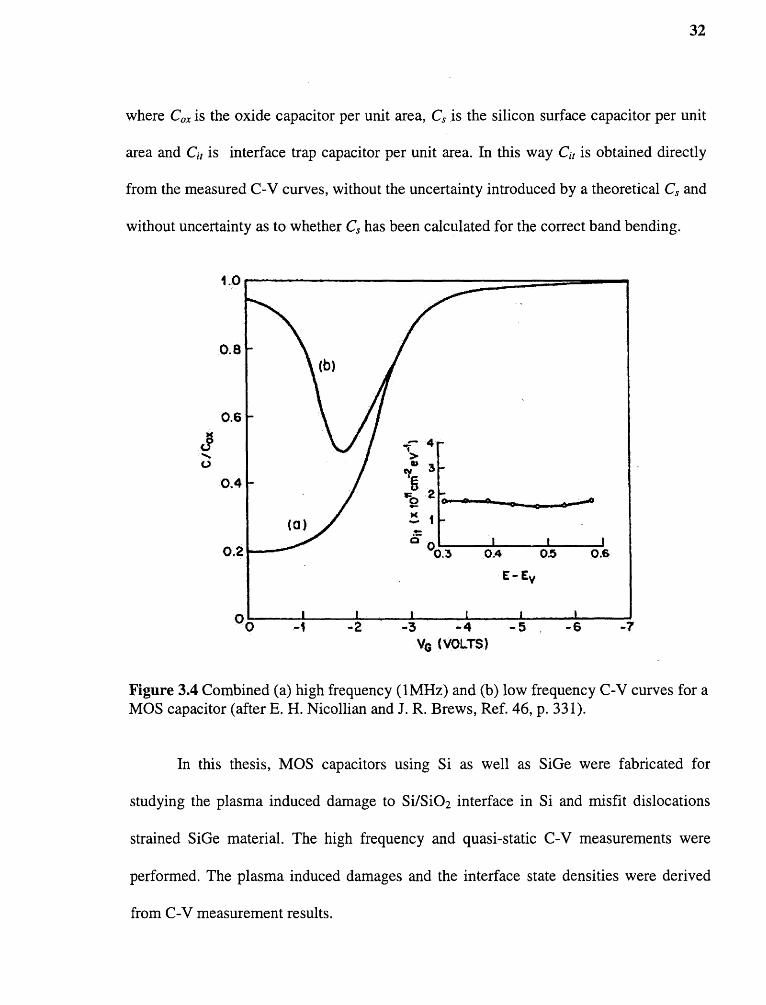
32
where Car is the oxide capacitor per unit area, Cs is the silicon surface capacitor per unit
area and Chit is interface trap capacitor per unit area. In this way Chit is obtained directly
from the measured C-V curves, without the uncertainty introduced by a theoretical C5 and
without uncertainty as to whether Cs has been calculated for the correct band bending.
In this thesis, MOS capacitors using Si as well as SiGe were fabricated for
studying the plasma induced damage to Si/SiO 2 interface in Si and misfit dislocations
strained SiGe material. The high frequency and quasi-static C=V measurements were
performed. The plasma induced damages and the interface state densities were derived
from C=V measurement results.

33
3.2 Deep Level Transient Spectroscopy (DLTS) Techniques
Luminescence has been widely used with great success in the study of shallow centers.
But it misses the deeper non-radiative centers. The deep-level transient spectroscopy
(DLTS) is a high-frequency capacitance transient thermal scanning method useful for
observing a wide variety of traps in semiconductors. It is sensitive, rapid, and easy to
analyze [48]. The DLTS measurement system consists of a sensitive capacitance
measurement apparatus with good transient response, one or two pulse generators to
make rapid changes in the diode bias, a dual-gated signal integrator, and x-y recorder,
and a variable temperature cryostat. The presence of each trap is indicated by a positive
or negative peak on a flat baseline plotted as a function of temperature. The heights of
these peaks are proportional to their respective trap concentrations. The sign of each peak
indicates whether it is due to a majority- or minority-carrier trap, and the positions of the
peaks are simply and uniquely determined by the integrator gate setting and the thermal
emission properties of the respective traps. By the proper choice of the experimental
parameters it is possible to measure the thermal emission rate, activation energy,
concentration profile, and capture rate of each trap.
For simplicity, only the situation in p-type material and in an asymmetric nap
diode will be described here. In the quiescent state of the system the diode is reverse
biased and observable traps are within the depletion region. Thus the capture rates are
zero and the occupation of the level is determined by the thermal emission rates el and e2
of minority and majority carriers respectively. The steady electron occupation of a level
is

34
where N is the concentration of the trap. The capture and thermal emission rates for
minority carriers (electrons in this example) are cif and e l respectively. The capture and
thermal emission rates for majority carriers (holes in this example) are c2 and e2
respectively. An electron trap has to have el>> e2 and a hole trap e2>> el. The emission
rates are proportional to a Boltzman factor and thus depend exponentially on the energy
difference between the trap level and the conduction band (electron emission) and the
trap level and the valence band (hole emission). Because of this, electron traps tend to be
in the upper half of the gap and the hole traps in the lower half.
There are two main types of bias pulses (see Sigure 4.5), namely, an injection
pulse which momentarily drives the diode into forward bias and injects minority carriers
into the region of observation shown in Sigure 4.6, and a majority-carrier pulse which
momentarily reduces the diode bias and introduces only majority carriers into the region
of observation shown in Sigure 3.7.
The steady-state electron occupation during a bias pulse is
where cif is the minority-carrier (electron) capture rate proportional to the concentration
of injected minority carriers and c2 is the majority-carrier (hole) recombination rate
proportional to the majority-carrier concentration. In all the situations considered, the
capture rates are much larger than the emission rates, which can be neglected during the

35
bias pulse. An injection pulse which introduces a large enough number of electrons so as
to make ci>>c2 and overwhelm the trap emptying process will completely fill the trap
with electrons; such a pulse is called a saturation injection pulse. A majority=carrier
pulse, on the other hand, introduces only holes, and thus tends to empty all traps of
electrons, i.e., fill them with holes.
Figure 3.5 Typical time dependence involved in pulsed bias capacitance transients formajority- and minority carrier traps. The upper half is a majority-carrier pulse sequencewhile the lower half is an injection-pulse sequence (after D. V. Lang, Ref. 48).

36

37
The concentration of a trap can be obtained directly from the capacitance change
corresponding to completely filling the trap with a saturating injection pulse (in the case
of minority-carrier trap) or the largest possible majority-carrier pulse (in the case of a
majority-carrier trap). The relationship for an electron trap in a n+ -p step junction is
simply
where N is the trap concentration, AC is the capacitance change at t=0 due to a saturating
injection pulse, C is the capacitance of the diode under quiescent reverse=biased
condition, and NA-ND is the net acceptor concentration on the p side of the junction where
the trap is observed.
The essential feature of DLTS is the ability to set an emission rate window such
that the measurement apparatus only responds when it sees a transient with a rate within
this window. Thus if the emission rate of a trap is varied by varying the sample
temperatures, the instrument will show a response peak at the temperature where the trap
emission rate is within the window. The emission rates are thermally activated and by the
principle of detailed balance can be given as
where o is the minority-carrier cross section, <vi > is the mean thermal velocity of
minority carriers, NDl is the effective density of states in the minority-carrier band, Al is

38
the degeneracy of the trap level, and AE is the energy separation between the trap level
and the minority-carrier band. An exactly similar equation holds for e2 with subscripts
changed from 1 to 2 and with all quantities referring to majority carriers. A standard
means of characterizing the depth of a trap is to construct a plot of loge/ or loge 2 vs.
1000/T and to report the slope of the resulting straight line as the activation energy of the
trap.
Figure 3.8 Illustration of how a double boxcar is used to define the rate window. Theleft-hand side shows capacitance transient at various temperatures, while the right-handside shows the corresponding DLTS signal resulting from using the double boxcar todisplay the difference between the capacitance at time t1 and the capacitance at time t2 asa function of temperature (after D. V. Lang, Ref. 48).
The emission rate corresponding to the maximum of a trap peak observed in a
DLTS thermal scan is

39
This can generate one point of loges- or loge 2- vs —1000/1 plot. Other points can simply
be obtained from other scans made with different gate settings and thus different values
of r„,,„- and different trap peak positions.

40
The DLTS technique has been used in this research for Si MOS capacitor and
SiGe/Si p+-n diode. It provides the information about process induced electrical defects at
the silicon and silicon dioxide interface and detects any process induced defects and
misfit dislocations at the Si/SiGe interface. The equations described here have been
applied to calculate the trap concentrations and the energy level of these traps.

41
3.3 Physical Characterization
3.3.1 Secondary Ion Mass Spectroscopy (SIMS)
In the SIMS method, an ion beam sputters material off the surface of a sample, and the
ionic component is mass analyzed and detected (Figure 4.10). Sputtered ions are
extracted and mass analyzed with a magnetic prism or quadrupole analyzer. In a system
that uses a magnetic prism, a two-dimensional image of the distribution of an ionic
species across the surface can be obtained by directing the secondary ion beam onto a
channel plate. In quadrupole instruments the image is formed by recording the changing
secondary ion-beam current as primary beam is rastered across the sample surface. The
intensity of the detected signal is related to the mass concentration. The mass spectrum
can be displayed as a function of time, giving a depth profile of the chemical species.

42
Both positive and negative incident ions are used with a beam energy typically
between 5 and 15 keV. Since only the ionic fraction of sputtered material produces a
SIMS signal, ion beams are chosen that produce the highest ion yields of the species
under study. Positive cesium ion beams are generally useful for producing high negative
ion yields of electronegative species from a target, and 02+ ion beams are usually used
for generating high positive ion yields from electropositive species.
The incident beam is rastered across a small area of the surface to create a crater
with a nearly flat bottom. Mass analysis is performed on the ionic fraction of sputtered
material only from a central portion of crater. When very low primary ion currents are
used, sputtering rate are lowered to the point where data can be collected from a few
monolayers, and surface analysis can be performed. Depth profiles are obtained by using
higher primary ion currents. Lateral spatial resolution depends on the type of ion optics
used in the instrument. Increased resolution must be traded off with sensitivity. SIMS
achieves lateral resolution of about 0.5 gm which is useful for the analysis of some
patterned VLSI chips. Vertical (depth) resolution is controlled by many factors, such as
texture at the bottom of a crater, the contribution of signals from the crater wall, and
impurity redistribution during ion milling.
3.3.2 X-Ray Photoelectron Spectroscopy (XPS)
X-ray bombardment of a sample can stimulate the emission of core-level electrons if the
incident x-ray energy is sufficiently high. Letting E0 be the energy of the incident x-
radiation, Eb the binding energy of the emitted electrons, AO the work function difference

43
between the samples and spectrometer surface, and E xp the energy of the emitted electron
(photoelectron kinetic energy),
With constant AO and E, in a given experiment, electrons of different binding
energies give rise to separate peaks in the photoelectron spectrum. The application of this
phenomenon to chemical analysis of the bombard surface is called x-ray photoelectron
spectroscopy (XPS); this procedure is also called electron spectroscopy for chemical
analysis (ESCA).
The incident x-ray beam is usually generated by low-energy electron
bombardment of an aluminum or magnesium anode. Ka radiation from magnesium has an
energy of 1254.9 eV and a linewidth of 0.7 eV, and Ka radiation from aluminum has an
energy of 1487.0 eV and linewidth of 0.85 eV. Since AO is about 1 eV, photoelectron
energies from aluminum or magnesium sources are sufficiently low so that escape depth
are less than 50A. XPS therefore provides chemical information from a region within a
few monolayers of the surface.
XPS is often used as a complement or back-up to AES, because of the following
three advantages. Sirst, radiation sensitive material can be nondestructively studied,
because the scattering cross section for x-ray induced desorption and dissociation are
significantly lower than the corresponding cross sections for electron bombardment.
Second, insulators can be studied with less surface charging, since a neutral incident
beam is used. The energy levels of core electrons are affected by valence state and type
of chemical bonding. The energy resolution of XPS peaks is typically about 0.5 eV, and
since different chemical bonds often produce shifts in the binding energy by larger
amounts, these shift can be detested and bond identified [49].

44
3.3.3 Transmission Electron Microscopy (TEM)
Transmission electron microscopy (TEM) is a useful tool for solving problems in VLSI
technology that require high spatial resolution. TEM offers a resolution of about 2A. In a
transmission electron microscope an electron beam passes through the thin-film sample,
and forms an image that displays morphological and crystallographic features of the film
components. Commercial TEM instruments use electron beams with energy between 60
and 450 keV. Higher beam energy permits greater sample penetration; the maximum
thickness of silicon which permits TEM image formation is 1.5 gm for 200 keV beam,
but only 0.5 p.m for an 80 keV beam.
Contrast in a TEM image can be described for two situations. One is TEM study
of crystalline materials (such as silicon, aluminum, polysilicon, and various silicides),
and the other is the study of amorphous materials. In crystalline materials, the incident
electron beam is diffracted by the material and local variations in diffraction intensity
produce contrast in an image from the undiffracted beam (bright field image) or from one
or more diffracted beam (dark field image). The intensity of the emergent beam is
periodic with sample thickness. The sample thickness corresponding to one period or
more in silicon is 60.2 nm for a (111) reflection and 75.7 nm for a (220) reflection [50].
Thus, a thicker region of the sample does not necessarily look lighter in the negative;
wedge-shaped crystalline sample produces a TEM image that has alternate light and dark
bands called thickness extinction contours. Dark bands are also caused by a bent sample
and are then called bend extinction contours. Abrupt changes in thickness, phase
structure, or crystallographic orientation cause corresponding abrupt changes in contrast,
and these crystallographic features can be easily imaged at high resolution.

45
In the case of nearly amorphous material, contrast is determined by local changes
in electron scattering which result from differences in sample thickness or from
differences in chemical or phase composition. A sample region whose thickness varies
continuously produces a corresponding continuous variation in image intensity, unlike
the case of diffraction contrast. TEM images obtained from oxides, nitrides, and other
amorphous materials are therefore somewhat easier to interpret intuitively than images
obtained from crystalline samples.

46
3.4 Simulation of Sii,Ge. Device for Damage Estimation
3.4.1 Overview of Device Simulator
Atlas is a physical-based device simulator. Physical-based device simulators predict the
electrical characteristics that are associated with specified physical structures and bias
conditions. This is achieved by approximating the operation of a device onto two or
three-dimensional grid, consisting of a number of grid points called nodes. By applying a
set of differential equations, derived from Maxwell's laws, onto this grid it is possible to
simulate the transport of carriers through a structure. This means that the electrical
performance of a device can be modeled in DC, AC or transient modes of operation.
Physical-based simulation provides three major advantages: it is predictive, it
provides insight, and it captures theoretical knowledge in a way that makes this
knowledge available to non-experts. Physical-based simulation is different from
empirical modeling. The goal of empirical modeling is to obtain analytic formulae that
approximate existing data with good accuracy and minimum complexity. Empirical
models provide efficient approximation and interpolation. They do not provide insight, or
predictive capabilities, or encapsulation of theoretical knowledge. Physical-based
simulation is an alternative to experiments as a source of data.
Physical-based simulation has become very important for two reasons. First, it is
almost always much quicker and cheaper than performing experiments. Second, it
provides information that is difficult or impossible to measure. The drawbacks of
simulation are that all the relevant physics must be incorporated into a simulator, and
numerical procedures must be implemented to solve the associated equations.

47
The steps of using the physical-based simulation include defining the physical
structure, defining the physical models to be used and defining the bias conditions for
which electrical characteristics are to be simulated.
3.4.2 Important Physics and Equations in SiGe MOS Simulation
Many years of research into device physics has resulted in a mathematical model of the
operation of any semiconductor device. This model consists of a set of fundamental
equations which link together the electrostatic potential and the carrier densities, within
some simulation domain. These equations, which are solved inside any general purpose
device simulator, have been derived from Maxwell's laws and consist of Poisson's
equation, the continuity equations and the transport equations. Poisson's equation relates
variations in electrostatic potential to local charge densities. The continuity equations
describe the way that the electron and hole densities evolve as a result of transport
processes, generation processes, and recombination processes.
Traps and Defects
Semiconductor materials exhibit crystal flaws which can be caused by dangling bonds at
interface or by the presence of impurities in the substrate. The presence of these defect
centers, or traps, in semiconductor substrates may significantly influence the electrical
characteristics of the device. Trap centers, whose associated energy lies in a forbidden
gap, exchange charge with the conduction and valence bands through the emission and
recombination of electrons. The trap centers change the density of space charge in
semiconductor bulk and influence the recombination statistics.

48
Device physics has established the existence of three different mechanisms which
add to the space charge term in Poisson's equation, in addition to the ionized donor and
acceptor impurities. These are interface trapped charges, interface trap states and bulk
trap states. Interface trapped charge is modeled as a sheet of charge at the interface and
therefore is controlled by the interface boundary condition. Interface traps and bulk traps
will add space charge directly into the right hand side of Poisson's equation.
Two basic types of trap have been found to exist; donor-like (electron traps) and
acceptor=like traps (hole traps). A donor-like trap, similar to ionized donor impurities
ND+ , is positively charge and therefore can only capture an electron. This means that
donor-like traps are positive when empty of an electron but are neutral when filled. An
acceptor-like trap, similar to ionized acceptor impurities N A- , is neAative when filled but
are neutral when empty. In a semiconductor there is a position of the Sermi level
corresponding to neutrality. At this condition, those traps above the Sermi level are
defined as acceptor-like and those below the Semi level are donor-like. The position of
the trap is defined relative to the conduction or valence bands using E.LEVEL in ATLAS.
Poisson's Equation
Poisson's equation including the carrier concentrations, the ionized donor and acceptor
impurity concentrations ND+ and NA, charge due to traps and defects, BT has the form:
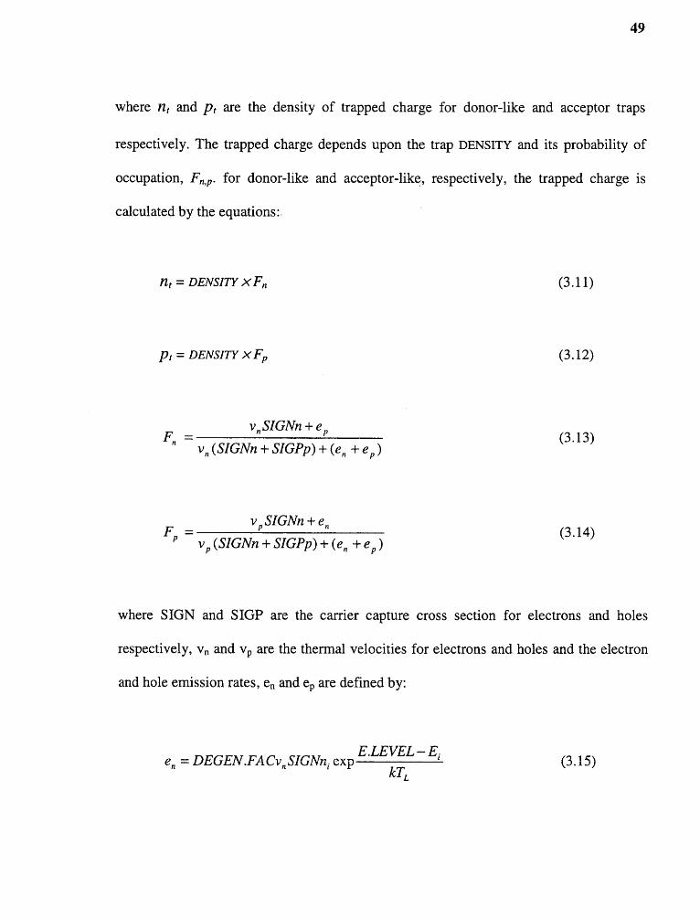
49
where n t and p t are the density of trapped charge for donor-like and acceptor traps
respectively. The trapped charge depends upon the trap DENSITY and its probability of
occupation, Fn ,p. for donor-like and acceptor=like, respectively, the trapped charge is
calculated by the equations: .
where SIGN and SIGP are the carrier capture cross section for electrons and holes
respectively, vn and vp are the thermal velocities for electrons and holes and the electron
and hole emission rates, e n and ep are defined by:

50
where Ei is the intrinsic Fermi level position, E.LEVEL is the energy level in the bandgap
of each discrete trap center and DEGEN.FAC is the degeneracy factor of the trap center.
The latter term takes into account that spin degeneracy will exist, that is the "empty" and
"full" conditions of a flaw will normally have different spin and orbital degeneracy
choices.
3.4.3 Simulation of Sii..Ge. MOS Capacitor Using Silvan Device Simulator
Sirstly, use Silvaco's DevEdit to create the 2D MOS device structures (as shown is
Sigure 4.11), generate the mesh (Sigure 4.12) and save it as a structure file. This structure
file, which contains device dimension and defined material, will be loaded into Atlas for
simulation. The structure used in simulation is similar to that of a conventional MOS
capacitor, except for the present of the Sii_„Ge, channel, separated from the Si/Si02
interface by a Si cap layer.

51
lum
" Al 10tun
Si 02 40nm
Si Cap 40nm NA=1x10
Si i ,Ge„ (x=15%) 50nm NA=1x10
Si sub 1000nm NA=2x 10 16
3um
DEVEDIT
Data from pMOS SiGe.str
2 2.4 2.8
Figure 3.11 SiGe MOS capacitor structure used for simulation.
Figure 3.12 Simulated device structure with mesh.

52
Secondly, use Silvaco's Deckbuilder to create an Atlas input file. There are five
groups of statement in this file, and these must occur in the correct order. These groups
are indicated in Sigure 4.14. The input file for this example is shown in Appendix.
Figure 3.13 Atlas command group with primary statements in each group [Ref. 51].
Sinally, run the simulation and use the Tonyplot to interpret the results. Sigure
4.14 shows the simulated C-V plot. Sigure 3.15 shows the energy diagram cross the MOS
capacitor.

53

54
Figure 3.15 Vse Tonyplot to display the energy diagram cross the MOS capacitor undercertain bias condition.

CHARPTER 4
ETCH-INDUCED DAMAGE TO MOS DEVICEIN HIGH-DENSITY ICP ETCHING REACTOR
4.1 Introduction
Inductively coupled plasma (ICP) sources are able to operate at lower pressures (1-20
mTorr) and can produce plasma densities in the 1 x 10 11 - 1 x10¹² ions cm"3 range [52, 53] .
They are capable of uniform etching of anisotropic features over large area wafers at etch
rates comparable to conventional high-pressure capacitively coupled reactive ion etching
(RIE) tools. The ion energies incident on the wafers can be effectively decoupled from
plasma generation by independently applying RF power to the wafer chuck. However, a
fundamental understanding of the etch induced damage to thin gate oxide in these types
of etching source is required to enable their widespread acceptance by integrated circuit
manufactures.
Plasma etching can cause oxide charging where charges are trapped in the oxide
and surface state are created at the Si=SiO2 interface, thereby deforming the C-V
characteristics of the gate oxide. However, the physical nature of those charge traps is not
well understood. By identifying the type of defect created in the oxide by the etching
process, one can more easily investigate ways to make gate oxides more resistant to such
damage. This research correlates plasma induced electrical damage to thin gate oxide
with that of the physical damage during polysilicon etching in an ICP etcher leading to
the development of a basic understanding of damage. The electrical measurements were
carried out using high frequency, quasi-static C-V and DLTS measurements (see Chapter
3 for more details) whereas physical damage was investigated using x-ray photoelectron
spectroscopy.
55

56
4.2 EDperimental Details
Sigure 4.1 shows the high=density ICP reactor configuration used in this work. A
patented RF coil used in this source has flat and solenoidal excitation section and
produces remarkably uniform plasma with uniformity better than ±5% over 200 mm. Due
to unique coil geometry, this source appears to have a greater B field or inductive
coupling and lower E field or capacitive coupling than conventional flat (pancake type)
sources. The RF coil design contributed to the uniformity due to higher degree of
inductive coupling over a large power and pressure range. The uniformity was measured
using a Langmuir probe.
In this reactor the gap between the ICP and RF electrodes was 4 in (10.16 cm) and
ICP coil was water-cooled. Vnder the condition used for etching in this reactor, the phase
difference between the inductive source and RS source has minimal effect. The change in
induced bias on the RF electrode was less than 2% when the phase was varied between 0
and 460°. The etch selectivity of polysilicon on oxide in this reactor with the etching
condition (power, pressure, gas and distance) is in the range of l5:1 to 20:1.
Wafers with 500 nm thick n-doped polysilicon on l5nm thick oxide were etched
in this reactor at various wafer biasing conditions (as listed in table 4.1) in SF6/02
plasma.

57
At low pressure (1-5 mTorr) the electronegativity of SFr is not a problem for
polysilicon etching. The wafer electrode was floating when ICP power was activated
alone. The dc bias was +16 V for this condition (sampled) whereas when the wafer
electrode was powered the dc bias was negative (Table 4.1). The induced dc bias was
measured with a RF choke, a capacitor filter and a resistive voltage divider. The +16 V

58
on the floating electrode (dc or time averaged floating potential) is with respect to earth
and not with respect to the plasma potential. It is expected that the plasma potential is
more positive with respect to this floating potential. When the wafer electrode is not
powered (the substrate is at floating potential) the electron flux to the substrate is much
greater as compared with RF bias etching. This is because for a floating electrode the
U.., (*Gill
where nee is the electron density in the plasma, e is the electronic charge, K is tine
Holtzman constant, Te is the electron temperature and p , Bf and Vdc are the absolute
value of the plasma potential and the bias electrode potential respectively. Since p - Vf< <
p - Vde and the mean free speeds are nearly equal ( Cep = C 2 ) to maintain the charge flux
balance at the electrode [54, 55],

59
Thus, the number of electrons arriving at the floating electrode is much higher as
compared to the biased electrode. The number of ions arriving at the sheath edge nib stays
nearly the same due to space charge limited ion current. Though the above analysis is for
dc plasma, for rf plasma the same analysis holds true. In addition, the electrons that reach
the floating electrode suffer an e(Vp-Vf) loss of kinetic energy in crossing the sheath,
which is much smaller compared to the biased case. Therefore, the electrons in the biased
case have energies greater than the electrons in the biased case when they arrive at the
electrode surface. Because of the large electrons flux the measured dc bias was positive
whereas during rf bias conditions dominant ion flux to the surface developed a negative
dc bias.
Wet oxidation was used to grow the thin oxide (15nm) at 900°C on cleaned
silicon wafers. Doped polysilicon was then deposited by LPCVD. The end-point of
polysilicon etching was determined using a He-Ne laser interferometer with 10% over-
etch. A control wafer (sample #1) was prepared by wet etching polysilicon in KOH at
75°C. MOS capacitor structures were formed by evaporating Al dots (400 um and 600
um in diameter) in a resistive heating vacuum evaporator using a shadow mask on one
half of the area of the wafer for electrical characterization. The 400 gm diameter
capacitors were used for high frequency, quasi-static C-V and DLTS measurements and
600um diameter dots were used for oxide breakdown measurements.
The other half of the area of the wafers was used for physical characterization
using XPS. Each wafer was cleaved into several samples and separately analyzed to
verify the uniformity of etch results. Spectra typical for each etching condition are
reported. The samples were transferred in air from etching facility to the XPS instrument.

60
All spectra were obtained using unmonochrômatized Al Ka radiation. XPS was
performed both before and after annealing to 250°C in VHV and no significant changes
were observed.
4.3 Measurement Results
4.3.1 C-V Measurements
Normalized high-frequency C-V curves for various MOS samples immediately after
aluminum deposition (before any metal annealing) are shown in Figure 4.2(a) where the
flat band voltages were measured. The corresponding positive charge densities in the
oxide for samples 1-5 are measured and compared. Highest charging effects were
observed for the sample without any wafer bias (sample d) and an increase in charging
effect was also observed for increase in wafer bias (sample #4 being the lowest and
sample #5 being the highest). These samples were then annealed at 280°C for 10 min in
N2 ambient [56] to eliminate any charging effects that was created at the metal-oxide
interface during metal evaporation. Sigure 4.2(b) shows the high=frequency C-V
characteristics of samples annealed after metal deposition. A recovery in flat-band
voltage was noticed for all samples. Taking the control sample (sample #1) as reference
flat-band voltage shifts (öVf) of —0.905, -0.67, -0.57 and —0.857 V were observed for
samples 2-5 respectively. The shift pattern of the flat=band voltage in both unannealed
and annealed samples remained the same, which indicates the presence of a considerable
amount of oxide charge due to plasma etching, though the interface stated between the
metal and the oxide annealed out during metal annealing. A strong presence of fast
interface states was also observed in the C-V curves for sample #2 compared with other

61
samples. In high-frequency C-V measurements the effects of the interface states are
neglected as the interface trapped charge varies with gate bias whereas the fixed oxide
charge (r f) is independent of gate bias. The modification to the fixed oxide charge can
mainly due to the carrier trapping during etching. Besides, a small component of mobile
ionic charge (Q,n) might have been added due to sputtering of the sidewalls of the reactor.

Figure 4.2 Normalized C-V characteristics of various samples: (a) immediately aftermetal deposition; (b) after a 10 minutes annealing at 280°C in N2 ambient.
The quasi-static C-V measurement for annealed MOS capacitor including the
control sample (sample #1) are shown in figure 4.4. A strong deformation of C-V curves
is observed in sample d, indicating generation of interface traps during etching. The
damage to the interface in the above sample is possibly due to plasma induced electrical
charging effects produced mainly because of non-uniformity current stressing during the
over-etch process [57]. Though the current stressing due to plasma nonunifomity is very
small in the ICP reactor etch damage has occurred for minimal local nonuniformity. The
density of interface traps generated during plasma etching, when extracted from the
combination of high-frequency and quasi-static C-V curves, indicated plasma

63
nonuniformity in the case of sample d where a positive dc potential was induced (Table
3.1) at the floating rf electrode. The positive dc potential increased the electron flux
towards the wafer, producing lager damage to the oxide. An increase in the interface state
density Di, is noticed for the plasma etched samples. Di, of the control sample (wet
etched) in negligible whereas Di, values for samples 2 - 5 were 8.9x10" cm2 , 4.4x10"
cm2 , 2.4x10" cm2 and 8.1x10" cm-2 respectively. In addition, when the wafer bias was
increased (sample #5) the density of the interface traps increased as compared to sample
#4 and #4 as damage due to ion bombardment because dominant at higher rf power. No
increase in nonuniformity is noticed at higher biased in this reactor. Therefore, at a
constant ICP power the wafer bias should be minimum to reduce plasma etching induced
electrical damage to thin gate oxide in an ICP reactor.
Figure 4.3 Buasi-static C-V curves for MOS capacitors after plasma etching in an ICPreactor with different process conditions.

64
4.3.2 Breakdown Measurements
Figure 4.4 shows the breakdown distribution on samples immediately after aluminum
deposition. During the ramped voltage breakdown (RVBD) measurements, the Al gate
electrodes were biased negatively with respect to the substrate. The applied stress field
was increased by 0.5 MV/cm (200 ms/step) until the current exceeded 1.0 gA. It can be
noticed that samples with higher oxide charge density in Sigure 4.4 show a lower
breakdown field. The wet etched wafer (sample #1) exhibited the highest breakdown
field while the wafer with zero rf bias (sample #2) exhibited the lowest breakdown field.
For wafers etched under various biasing conditions (sample #4-5) the values of
breakdown fields were higher than sample d and were found to decrease with increasing
substrate bias power. The correlation between breakdown and positive charge trapping
can be explained by breakdown model that assumes that breakdown results from
enhancement of the electrical field at the interface due to the oxide charging.
Figure 4.4 The breakdown distribution of various samples.

65
4.3.3 DLTS Analysis
Representative DLTS spectra observed in the control sample (#1) and the plasma etched
sample (#4) are presented in figure 4.5. The quiescent voltage Ba and pulse voltage Vi
were 0.5 and —1.5V respectively. The spectra show a peak around 370 K for both sample
#1 and sample #4, which is attributed to minority carrier generation, since the peak height
increased with increasing quiescent bias voltage B a [58]. Comparing the two curves it can
clearly seen that interface traps have been created in sample #4 and no interface traps
were observed in the control sample (wet etched) at the same sensitivity.
The interface trap density N„ for sample #4 was calculated using the following
equations [58]:
where C(ti) and C(t2) are the capacitance transient values at times ti and t2 respectively,
Cox is the oxide capacitance per unit area, es is the dielectric constant of silicon, DA is the
substrate doping, sup is the capture cross section of the traps, Et and EV are trap energy
level and top of the valence band respectively, with is the thermal velocity of carriers, k is
Boltzmann's constant, T is the absolute temperature and Dv is the effective density of
states in the valence band.

66
Figure 4.6 Interface traps density N5 in the plasma etched sample (#4) as a function ofenergy.

67
DLTS measurements of the majority carrier band edge are limited by the response
time of the capacitance meter and by the lowest temperature the DLTS system can reach.
Also they are limited toward midgap by the minority carrier generation peak [59]. The
interface traps density (NN ss) can be measured for energy values 0.19 eV < E t — <0.37
eV. D„ for the plasma etched sample (#4) as a function of energy is shown in 4.6. The
trap density was obtained after taking a capture cross-section value of Gap =10-5 cm2 . The
N„ value obtained using DLTS technique is higher than the N„ value obtained using
quasi-static technique. This could be attributed to the fact that DLTS can be influenced
by energy and temperature dependence of the capture cross-section [60] or by the error of
combined high- and low- frequency technique. No bulk trap has been detected by DLTS.
4.3.4 XPS Characterizations
Figure 4.7 shows XPS spectra obtained from these samples. The peak near 104 eV
corresponds to stoichiometric SiO2 with silicon in the 4+ oxidation state [Si(4+)]. The
feature near 99 eV is from the Si substrate [Si(0)] under the oxide. The intensity between
100 and 104 eV corresponds to Si in oxidation states Si(n+) (n=1, 2, 4). These
intermediate oxidation states are typically associated with defective SiO2 where the bonds
between Si and (4=n) of its 0 neighbors in the SiO4 tetrahedral unit have been broken and
replaced by Si or some similar bonding. As can be seen from this figure 4.7 the density of
intermediate oxidation states is very similar for each process except for etching with
zero-bias power condition (sample #2).

68
To see whether all suboxides are produced uniformly, or whether some states are
preferred, the area under each peak is plotted in figure 4.8. To obtain the data, each Si 2p
spectrum was fitted to the sum of five Gaussian pairs, a pair representing the 2p1/2 and
2p4/2 spin orbit split components at an intensity ratio of 1:2 for each oxidation state. Sor
each spectrum, the same chemical shift, AE, i , and peak width for the Si(n+) oxidation
state was assumed* and fits were determined by minimizing x2 while varying the
intensity of each pair. A comparison of the percentage of total Si 2p intensity attributed to
each oxidation state yield essentially the same plot.

69
Although a quantitative comparison of the density of different oxidation states
cannot be made without correcting the cross section variation [61], the relative
concentration of a given oxidation state for each sample can be concluded directly. Sigure
4.8 clearly shows that the sample with zero bias (sample #2) has a significantly higher
density of Si (1+) states as compared to the other samples. This configuration is either an
Si bonded to a single 0 whose three other bonds are terminated by residual H
incorporated in the oxide during the wet oxidation process, or it represents the braking of
the bonding of a substrate Si to a bridging 0 at the Si-SiO2 interface.
Figure 4.8 XPS counts for various suboxide states.

70
4.4.1 Discussion of Results
In this study, damage to the thin oxide due to surface charging is noticed, even a device
does not have floating conductive gates, to concentrate the tunneling current at weak
region in the oxide during the overetch period [62-64]. A very uniform plasma obtained
in this reactor when the inductive power and rf power exist together, minimizes the
probability of surface charging. During the zero-bias condition, the substate is floating
and electron flux to the substrate is much greater as compared with rf biased etching. In
addition, even though a Langmuir probe was employed to study the nonuniformity, any
spatial resolution very close to the wafer surface could not be obtained and finer scale
nonuniformities beyond the sensitivity of the probe were also undetected. Therefore, it is
believe that either the damage is caused by the high-energy electron impact or due to the
existence of localized plasma nonuniformity when only rf coil was powered. The
nonuniform plasma could stimulate the accumulation of charges on gate electrode. These
stored charges can cause an electric breakdown of the thin gate oxide [72]
A possible mechanism is that the high electron flux causes tunneling current to
flow through the thin oxide. This tunneling current can induce surface states at Si-SiO2
interface and trap charge in oxide [62, 64]. It is interesting to note that previous attempts
to study radiation damage with low-energy electron beams have found [65] enhancement
of the Si(4+) oxidation state as opposed to the Si( 1+) as observed here. This may be due
to energy of the bombarding electrons generated in the plasma, or it may be the results of
a cooperative effect from simultaneous electron and ion bombardment.

71
43 Summary
Electrical damage to the thin oxide during etching was found in good agreement with the
physical damage. Srom the XPS study, it can be concluded that degradation of the thin
oxide is associated with creation of suboxidation state. Besides, the major possible
mechanisms responsible for damage in this study appear to be high-energy electron
charging when only the ICP power is activated without any bias power applied to the
wafer carrying electrode. Energetic ion bombardment damage is dominant when the
wafer-carrying electrode is biased and in the condition the damage increases with
increases in power rf bias.

CHAPTER 5
PLASMA INDUCED DAMAGE TO STRAINED Sii.x Ge
5.1.1 Electrical Studies on SF6 and 0 2 Plasma Etched Sii,Ge. p-n Heterojunction
In this study, the electrical measurements I-V & C-V characteristics of wet etched, Fr
plasma etched, un-etched and 02 ashed samples of Sii_„Gex p-n heterojunction were
presented. These electrical evaluation methods can serve as very sensitive qualitative
measurements of heterojunction quality. In addition, material characterizations of these
samples by SIMS and TEM have been performed.
The Sii_„Gex wafers used for this experiment were grown by RTCVD techniques.
An n-type (As doped) silicon (1x10 16 cm3 ) layer (500nm) was first grown on a n+=Si
substrate. Then a p-type (1x10 19 cm-3 ) strained Si0.86Ge0 . 14 epitaxial layer (40 nm) was
grown on it at 900°C for 20 seconds. Sinally, a 120nm p-silicon (1x10 16 cm3 ) cap was
deposited (Figure 5.1 and Figure 5.2). The wafer was cut into several pieces. Then went
through different processes to study the plasma etching damage and contamination
effects.
72
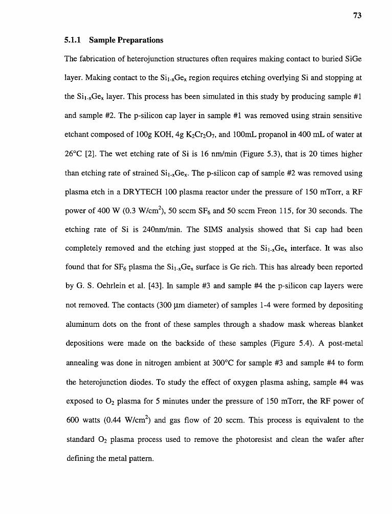
73
5.1.1 Sample Preparations
The fabrication of heterojunction structures often requires making contact to buried SiGe
layer. Making contact to the Si i_„Ge„ region requires etching overlying Si and stopping at
the Sii_xGex layer. This process has been simulated in this study by producing sample #1
and sample d. The p-silicon cap layer in sample #1 was removed using strain sensitive
etchant composed of 100g KOH, 4g K2Cr207 , and 100mL propanol in 400 mL of water at
26°C [2]. The wet etching rate of Si is 16 240nm/min (Figure 5.4), that is 20 times higher
than etching rate of strained Si i ,Gex . The p-silicon cap of sample #2 was removed using
plasma etch in a DRYTECH 100 plasma reactor under the pressure of l50 mTorr, a RF
power of 400 W (0.3 W/cm 2), 50 sccm SSr and 50 sccm Freon 115, for 40 seconds. The
etching rate of Si is 240nm/min. The SIMS analysis showed that Si cap had been
completely removed and the etching just stopped at the Sii_„Gex interface. It was also
found that for SFr plasma the Si i ..,,Gex surface is Ge rich. This has already been reported
by G. S. 0ehrlein et al. [44]. In sample #4 and sample #4 the p-silicon cap layers were
not removed. The contacts (400 gm diameter) of samples 1=4 were formed by depositing
aluminum dots on the front of these samples through a shadow mask whereas blanket
depositions were made on the backside of these samples (Figure 5.4). A post-metal
annealing was done in nitrogen ambient at 300°C for sample #3 and sample #4 to form
the heterojunction diodes. To study the effect of oxygen plasma ashing, sample #4 was
exposed to 02 plasma for 5 minutes under the pressure of l50 mTorr, the RF power of
600 watts (0.44 W/cm2) and gas flow of 20 sccm. This process is equivalent to the
standard 02 plasma process used to remove the photoresist and clean the wafer after
defining the metal pattern.

74

Figure 5.4 Device structures were used for study and comparison.
75

76
5.1.2 Current-Voltage Measurements
I-V characteristics of the wet etched sample #1 and plasma-etched sample #2 are shown
in the Figure 5.5. The I-V degradation has the following features: 1) in the initial region,
the current level of the plasma etched sample is higher than the wet etched sample for a
given voltage. This indicates that higher recombination current has been generated. 2) at
higher biases where the diffusion component is stronger, the current level of the plasma
etched sample drops below that of wet etched sample. During the plasma etch, the Sit_
xGex might have been partially relaxed by forming misfit dislocations. Therefore, the
band gap of the Sii_„Ge x layer would increase which would reduce the current level [66].
4) a degradation in the non-ideality factor in noticed (from 1.4 to 2.2) after etching
indicating a recombination dominance in the forward characteristics because of
generation of more recombination sites caused by stress during plasma etching.
Figure 5.5 The I-V characteristics of wet etched sample #1 and SF6 plasma etchedsample d.

77
5.1.3 C-V Measurements
C-V measurement of the wet etched sample #1 and SF6 plasma etched sample d are
shown in the Sigure 5.6. This also confirms that the SF6 etching has negative effect. The
capacitance is higher than the wet etched samples. This is because dry etching damages
the sample and creates electrically active states in the depletion region. Interface charges
in the electrically active stated can contribute to a parasitic capacitance (C s) which acts in
parallel to the depletion capacitance (Cd) [67-69]. Therefore, the overall capacitance is
higher than the wet etched samples.
Figure 5.6 The C-V characteristics of wet etched sample and SF6 plasma etched sample.
5.1.4 TEM Analysis
Through the use of TEM, it was found that dislocation loops were formed in Si/Sii,Ge x
/Si outside the aluminum region due to the ion bombardment stress. The density of the

78
dislocation loops is low —1.9 x10 1° cm2 . The loops are between 1-1.4 nm in size, and
extend 238 nm deep (Sigure 5.7(b)).
5.1.5 Effects of 02 Plasma Ash Process
I-V characteristics of the un-etched sample #4 and 02 plasma bashed sample #4 are shown
in Figure 5.8. The difference in the I-V characteristics between two samples was not at all
substantial. This is because of the Si/Sii_„Ge x /Si was not directly exposed to the plasma.
Si/Sil_„Gex/Si had been shield by aluminum layer. The forward current of 02 bashed
sample is slightly lower than that of the un-etched sample. This is might be due to an
increase in the series resistance of the ohmic contact caused by plasma electrical stress.
C-V profiles for sample #4 and #4 are almost identical.

79
Figure 5.8 The I-V characteristics of un-etched sample #4 and 0 2 plasma ashed sample#4.
5.1.6 Summary
SF6 plasma was used to etch an overlying Si film stopping at the Si i _„Gex strained film.
This can cause electrical damage to Sii_„GelSi heterojunction device. The damage is
mainly because of ion bombardment and radiation-induced bonding changes. Plasma
etching creates interface charges and more recombination centers that can give higher
depletion capacitance, and decrease the diffusion current. The 0 2 plasma has no strong
effect on the Si i ,Gex device when the device is protected by its aluminum contact layer.
That is good for Sii_xGe. device process.

80
5.2 Evaluation of Plasma Process-Induced Bandgap Modificationof a Strained Sii.x Ge Heterostructure Using MOS Capacitor
In this study, a capacitance-voltage (C=V) profiling technique on Sii_ xGex MOS capacitor
to estimate the change of band gap of Sii_xGex film (grown on p-type substrate) exposed
to plasma etching and subsequent annealing process has been employed. C-V profiling is
a fast and efficient approach to estimate plasma process-induced band-gap modifications,
since measurement techniques such as photoemission measurement, x-ray photoelectron
spectroscopy, or photoreflectance measurement can be time consuming.
5.2.1 Sample Preparations
The typical structure of the MOS capacitor used in this study is schematically shown in
Figure 5.9. One characteristics of this structure is that the Sii_ xGex quantum well layer is
located within the depletion layer formed by gate bias. Thus, this device structure allows
the Fermi level at each hetero-interface to be varied by changing the gate voltage and, as
a result, allows the position where holes are accumulated to be controlled, as described
below.

81
Vnder the slight depletion condition, as shown in Figure 5.10 (a), the surface of
the top Si is depleted and holes are accumulated only in the Sii_„Ge x well. Under the
strong accumulation condition (Figure 5.10 (b), holes are accumulated both in the top Si
surface layer and in the Sii..,,Gex well region. When the magnitude of the negative gate is
sufficiently large, the incremental charges associated with ac gate voltage are formed
only into the accumulation layer of the Si top surface.
15% of Ge is used to grow strained Sii_„Ge x film for high-mobility advantage.
Undoped 50 nm thick Sii.,,Gex (x=0.15) was grown on a p-Si (2x10 16 cm3 ) substrate by
conventional chemical-vapor deposition (CVD) at 700°C at atmospheric pressure. A 150
nm thick Si cap layer was deposited on the layer. Plasma etching was performed
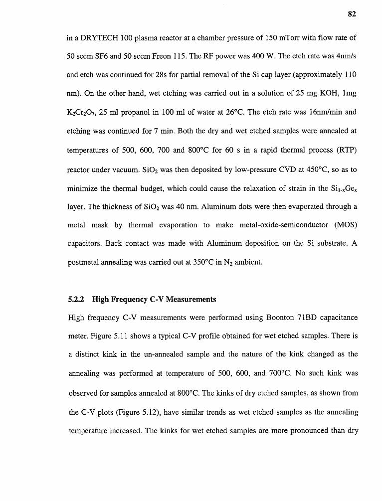
82
in a DRYTECH 100 plasma reactor at a chamber pressure of l50 mTorr with flow rate of
50 sccm SF6 and 50 sccm Freon 115. The RF power was 400 W. The etch rate was 4nmis
and etch was continued for 28s for partial removal of the Si cap layer (approximately 110
nm). On the other hand, wet etching was carried out in a solution of 25 mg KOH, lmg
K2Cr207 , 25 ml propanol in 100 ml of water at 26°C. The etch rate was 16nm/min and
etching was continued for 7 min. Both the dry and wet etched samples were annealed at
temperatures of 500, 600, 700 and 800°C for 60 s in a rapid thermal process (RTP)
reactor under vacuum. Si02 was then deposited by low-pressure CVD at 450°C, so as to
minimize the thermal budget, which could cause the relaxation of strain in the Sii_xGex
layer. The thickness of Si02 was 40 nm. Aluminum dots were then evaporated through a
metal mask by thermal evaporation to make metal-oxide-semiconductor (MOS)
capacitors. Back contact was made with Aluminum deposition on the Si substrate. A
postnatal annealing was carried out at 450°C in N2 ambient.
5.2.2 High Frequency C-V Measurements
High frequency C-V measurements were performed using Boonton 7lBD capacitance
meter. Sigure 5.11 shows a typical C-V profile obtained for wet etched samples. There is
a distinct kink in the un-annealed sample and the nature of the kink changed as the
annealing was performed at temperature of 500, 600, and 700°C. No such kink was
observed for samples annealed at 800°C. The kinks of dry etched samples, as shown from
the C-V plots (Sigure 5.12), have similar trends as wet etched samples as the annealing
temperature increased. The kinks for wet etched samples are more pronounced than dry

83
etched samples under same annealing condition. These C=V plots had flat band
corrections.

Figure 5.12 Typical C-V profiles obtained for the dry etched samples.
5.2.3 Device Simulation
It has been reported that the kinks are due to the present of strained Sii.. xGex layer [45].
When the Sii_xGex /Si MOS is driven form slight depletion to accumulation mode (Figure
5.10), holes are accumulated only in the Si i _xGex quantum well region. Since the total
capacitor equals the series combination of C ox and CSiGe well/ the total capacitance will be
smaller than the MOS capacitance without Si i _xGex well. When applied voltage becomes

85
more negative, more holes will be accumulated into the accumulation layer at the Si
02/Si interface instead of the Si i _„Gex well. The total capacitor will finally equal to Cox . If
the bandgap of strained Si i _xGe„ layer has been increased due to the relaxation after high
temperature annealing or plasma etching, the kink will be relatively smaller. When the
Sii_„Gex layer is completely relaxed, the Eg of Si i _„Gex will be as same as Si, no more
kinks will be observed. To verify this finding, several device simulations (using Silvaco's
Atlas) have been carried out. Table 5.l summarized the structures simulated in this
section. Sigure 4.11 shows the dimension of these structures.

86
** e.leve1=Et-Ev, where Et is the trap energy level and E v is the valence band energylevel.
Firstly, 01 and G2 structures have been simulated to see the effect of bandgap
increase due to plasma induced Sii_„Gex relaxation. From Sigure 5.14 it can be observed
that the kink from strained Sii_„Ge x is smaller than the observed data shown in Figure
5.11. That is because the valence band difference (4EV=0.11 eV) is not significant enough
to create a large kink during accumulation. In simulations, Eg=1.12 eV (same as Si) was
used for completely relaxed SiGe, while AE v=7.4x=111 meV [70] and Eg=1.12 eV were
used for strained Sii_„Ge,, (x=15).
The value of Cox, calculated using equation 5.2.l,
The calculated value 8.6x10 - 6
F./ is smaller than value of 9.2xl0 - 1 6 F/grn as shown in Figure 5.14. This is because
the top and bottom electrodes are not symmetrical in our simulation. If the top and
bottom electrodes have identical areas the calculated value matches the simulation result.
The fringing field effect normally neglected during the calculation of experimental
samples due to their large aspect ratio of Aid, but for these simulated structures it has to
be accounted for. The effective area A e1=9.2/8.6=1.07 gm.

87
Figures 5.14 and 5.15 can be used to explain the higher capacitance of strained
SiGe (Gl) compared to that of relaxed SiGe (G2) when the bias is from 0 to —lV (under
slight depletion region). Even though the Silicon buffer layer is still depleted, because the
energy difference (Ef-Ev) at back strained SiGe/Si interface is less compared to the
energy difference (Ef-Ev) in silicon buffer region (Figure 5.14), some holes start to be
accumulated in SiGe quantum well (Sigure 5.15). The incremental charges associated
with ac gate voltage are formed only in the SiGe quantum well. Since the effective
depletion depth is reduced to the thickness of silicon cap layer, the total capacitance with
quantum well is higher compared to completely relaxed film without quantum well.

88
Figures 5.16 and 5.17 can be used to explain the lower capacitance of strained
SiGe (Gl) compared to that of relaxed SiGe (G2) when the bias is from —1 to —l.25 V
(under slight accumulation region). That is because holes are still accumulated in SiGe
well instead of at SiO2/Si interface. The total capacitor, which equals to the combination
of Cox and CS1Ge well in series, becomes smaller compared to relaxed SiGe film without
quantum well.

89

90
Secondly, effects of Si02 fixed positive charges have been simulated with
structure G4, strained SiGe capacitor with fixed oxide charge of 2x10 11 cm2 . If the
energy level of donor trap is well above the Fermi level even at the large reverse bias
then the charge state of this trap is bias independent and it is referred to as "fixed charge
trap". The fixed positive charge produces a parallel shift of the C-V curve to the left (see
Sigure 5.18) by IVFB of 0.47 V which is in agreement with calculated result (Eq. 5.2.4).

91
where A,, B. and QQot are fixed=oxide charges, mobile ionic charges and oxide-trapped
charges respectively. If use equation 5.2.4 to calculate the effect of fixed charge (2x 10 11
cm2 ) on flat band voltage, the OVFB will be:
Thirdly, structures G4=G6 have been simulated to see the effects of interface trap
densities and their positions in the bandgap (Figure 5.19). The simulations have used the
single-level surface states. The device simulations show that the big steps or kinks from
measured C-V plots are mainly due to the present of donor-like interface traps at the low
temperature silicon oxide (ALTO). The trap has been predicted theoretically, by Tamm and

92
by Shockley [71], that because of disruption of the periodicity of the lattice at a surface, a
high density of state will be introduced into the forbidden gap near a semiconductor
surface. Such states have traditionally been called fast surface states. The charge in the
fast surface states will vary with the band bending or surface potential. At reverse bias
condition the quasi-Fermi level at top of cap Si is higher than the trap energy level, these
donor-like traps filled with electron and become neutral. When the quasi-Fermi level
moves lower than the trap energy level, these traps start to release the electrons and
become positive charges. Thus the increase of capacitor becomes slower and the step or
kink is created. After the interface traps released all trapped electrons, the depletion
decreases quickly when the reverse bias becomes more negative. The Capacitance
increases and finally equals C ox . The C-V curve after kink has the same shape as G1
(ideal Sii_,,Gex MOS capacitor) and only shifts to left due to these fixed charges and
positive charge from interface traps.
The step in the C-V curve moves up when the trap energy level moves closer to
valence band with constant trap density (G4 vs. G5). The C-V curve shifts to the right
side when the trap density reduces with constant trap energy level (G4 vs. G6). The flat
band voltage (VFB) of G4 and G6 are shifted by -0.94 V and -4.7 V respectively from G1
due to the total interface trap density of 5x10 -11 cm-2 and 2 x1012cm-2.

93
Finally, various interface trap densities, trap energy levels and fixed charges are
used to replicate the observed experimental results. Structures G8-G12 have been
simulated (Figure 5.20) to match the C-V plot in Figure 5.11. Structures G8-G12' which
have energy bandgap (E g) of 1.12 eV for SiGe layer to match the condition of relaxed
SiGe film have been added for comparison in Figure 5.21. Figure 5.21 shows that the
change in the shape of kink is caused by the interface charge reduction as well as
relaxation in SiGe film.

94

95
5.2.4 Discussion of Results
The presence of interface traps at poorly formed Si/SiO2 interface heavily influences the
C-V characteristics as evident from the simulation. Because the oxide was deposited at
low temperature the built-in fixed oxide charges are also higher. The effect of the fixed
charge can be determined by the flat band correction since the shift of the C-V curve is
parallel.
Figure 5.11 shows that the high temperature annealing (at 500 °C and 600 °C)
reduces the total interface trap density at SiO2/Si interface, while 700 °C annealing might
also reduce the energy level. The kink disappeared after the 800 °C annealing due to
complete removal of interface trap. This explanation has been simulated in Figure 5.20
using structure G8-G12 to replicate the measured plots in Figure 5.11.
High quality Si02 is necessary for using C-V profiling to detect the plasma
induced damages to Sii_„Ge x MOS capacitor. The simulations show that the interface trap
densities should be less than 10 11 cm"2. This would result in minimal distortion needed to
determine the valence band offset between the strained SiGe and Si. Thermally oxidized
silicon surfaces have relatively low density of fast surface states, but the process normally
requires high temperature (700=1200 °C), which could cause the relaxation of strain in
SiGe layer. If one tries to use LTO in the test structures, as done in this work, additional
Si control capacitors with no SiGe well need to be included to eliminate the effect of
interface effects in C-V measurement for extraction of integrity of strained SiGe film.
For SiGe MOS with moderate interface trap density, it may still use the C-V
profiling by expanding the coordinate of C-V curves at a slight depletion region where
the holes start to be accumulated in SiGe well due to the valence band offset at back
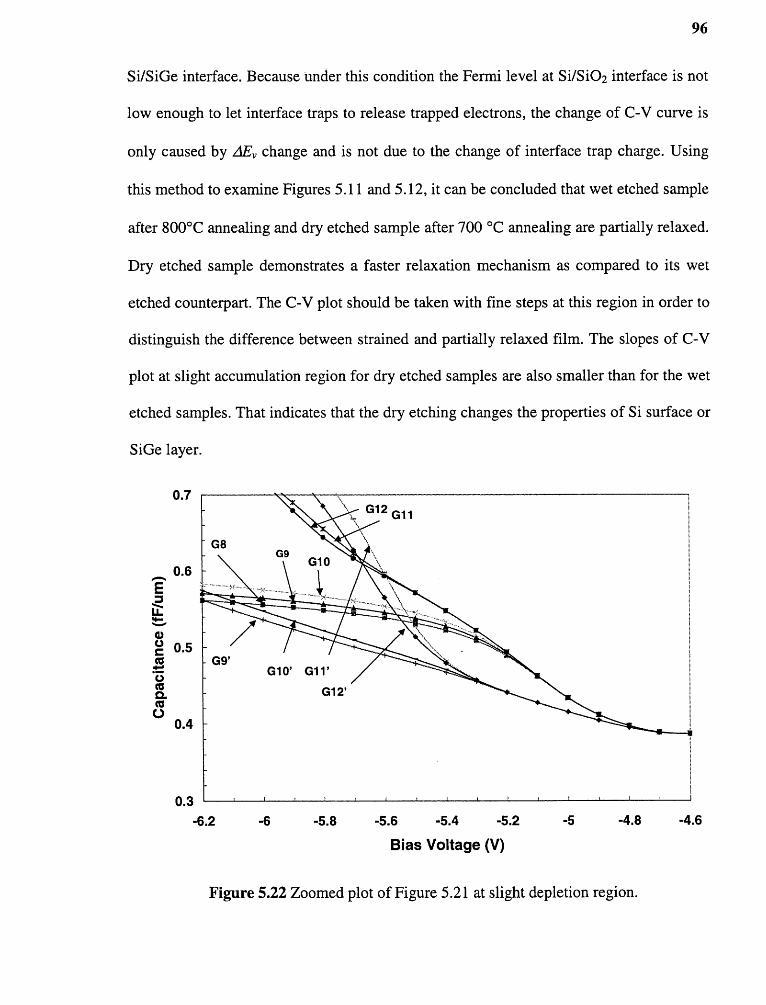
96
Si/SiGe interface. Because under this condition the Fermi level at Si/SiO2 interface is not
low enough to let interface traps to release trapped electrons, the change of C-V curve is
only caused by AEI change and is not due to the change of interface trap charge. Vsing
this method to examine Figures 5.11 and 5.12, it can be concluded that wet etched sample
after 800°C annealing and dry etched sample after 700 °C annealing are partially relaxed.
Dry etched sample demonstrates a faster relaxation mechanism as compared to its wet
etched counterpart. The C-V plot should be taken with fine steps at this region in order to
distinguish the difference between strained and partially relaxed film. The slopes of C-V
plot at slight accumulation region for dry etched samples are also smaller than for the wet
etched samples. That indicates that the dry etching changes the properties of Si surface or
SiGe layer.

97
5.2.5 Summary
C-V profiling has been applied to study the effect of plasma etching and subsequent
annealing on the valence-band discontinuity E„ at the Si/SiGe interface. The presence of
interface trap at Si02 deposited by low-pressure CVD process influences heavily to the
C=V profile at slight accumulation region. Both the reduction of trap densities and the
reduction of AE,, due to relaxation after annealing, affect the C=V profile at that region.
This makes the extraction of dE very difficult. The device simulations have been used to
confirm the findings and to provide the insights on the device operation. It indicates that
the interface trap has to be below 10 11 cm2 in order to use C-V profiling at slight
accumulation region to detect the E„ change after the plasma etching or high temperature
annealing. With moderate level of interface states (>10 11 cm2 ), the relaxation mechanism
can be probed using C-V measurement at slight depletion region (as shown in Figure
5.22). Dry etched sample demonstrates a faster relaxation mechanism as compared to its
wet etched counterpart due to the creation of dislocation loops by dry etching.

CHAPTER 6
CONCLUSIONS
This research has made two significant contributions in the area of evaluating plasma
induced damage: 1) application-oriented measurement of Si MOS capacitor for
evaluating the plasma induced damage processed by an advanced inductively coupled
plasma (ICP) reactor; 2) research-oriented measurements and simulations of strained
SiGe devices for gaining a fundamental understanding of plasma induced electrical and
physical damages to heterojunction material, and for developing a fast detection
technique.
Electrical characterizations such as C-V, RVH and DLTS measurements, and
physical analysis such as XPS were employed to investigate the plasma induced damage
to thin oxide processed by ICP reactor under different operating conditions. The shift of
flat band voltage, the reduction of breakdown voltage and the creation of high interface
trap density were found to be in good agreement with the creation of suboxidation states
at Si/Si02 interface. The major mechanism responsible for damage appeared to be high-
energy electron charging when only the ICP power was activated without any bias to the
wafer-carrying electrode. Energetic particle bombardment damage was dominant when
the wafer-carrying electrode was biased and the damage was considerable for rf bias
power greater than 35 W. A statistical distribution of breakdown voltage was used to
investigate the plasma induced damage in thin oxide.
The Fr plasma used to etch an overlying Si film stopping at the Sii_xGex strained
film caused electrical damage to an underlying Si i _„Gex/Si heterojunction device. The
changes of C-V and I-V characteristics, such as higher depletion capacitance and lower
98
99
diffusion current were attributed to ion bombardment and radiation=induced bonding
change, such as creation of interface charges and recombination centers. The TEM
analysis revealed the dislocation loops in Si/Sii_„Ge x /Si outside the aluminum region due
to the ion bombardment stress. The 02 plasma asking has no strong effect to Sii,Gex
device when the device was protected by aluminum contact layer.
C-V profiling has been applied to study the effect of plasma etching and
subsequent annealing on the valence-band discontinuity AZ at the Si/SiGe interface of
SiGe MOS capacitor. The presence of interface trap at Si02 deposited by low-pressure
CVD process created big kink at C-V profile at accumulation region. The change of C-V
profile was caused by the reduction of trap densities as well as the reduction of AEI, due
to relaxation after high temperature annealing. The interference from these traps made the
extraction of 4E, very difficult. The device simulations have been used to confirm the
findings and to provide the insights on device operation. By carefully evaluating the C-V
profile at slight depletion region the band gap modifications due to process-induced
damage could be distinguished. When compared with experimental results it was found
that the dry etched sample was partially relaxed after 700°C annealing and wet etched
sample was partially relaxed after 800°C annealing. Dry etched sample demonstrated a
faster relaxation mechanism as compared to its wet etched counterpart due to the creation
of dislocation loops in strained SiGe layer by dry etching process.
A PC based DLTS system has been developed to carry out this research. This
DLTS system is consists of MMR Technologies Cryogenic Cooling System, MMR
Technologies K-20 temperature controller and a vacuum pump, Boonton 7200
Capacitance Meter and a computer. A BASIC program was written to control the

100
temperature and to do the data acquisition through GPIB card and data acquisition card.
This extremely efficient transient data acquisition system allows a single transient to be
sampled up to 11 (or more) different sample rates without changing the hardware
configuration as compared using a conventional dual-gated signal averager (double
boxcar). This system is very useful for observing a wide variety of traps in
semiconductors.
6.1 Suggestions for Future Work
Several continuations and new directions are suggested by the present thesis.
The Atlas Device Simulator has demonstrated its effectiveness to explain and
predict the experimental results. It should be used extensively for future device design
and experiment design.
C-V profiling technique has potential application for estimating the change of
band gap of Si i_„Ge,, exposed to plasma etching and subsequent annealing process. This
application should be investigated with low trap density SiO2 as discussed in Chapter 5.
In addition to reducing the SiO2 interface trap density, the Si control capacitors without
Sii_„Gex well can be used as control samples. These control samples should go through
the same process steps as the SiGe MOS capacitors. The difference of C-V profile
between the SiGe and its Si counterpart will provide useful information for extracting the
ziEv after each process step. The measurements and simulations in appropriate regions
should be carried out with care and high resolution as shown in Figure 5.22.

101

102

REFERENCES
1. T. Tatsumi, H. Hirayama, and N. Arizaki, Appal. Phys. Lett. 52(11), 895 (1988).
2. J. C. Sturm, E. J. Prinz, and C. W. Magee, IEEE Electron Device Lett., Vol. 12, No.6,404 (1991).
3. S. Verdonckt-Vnderbroek et al., IEEE Electron Device Lett., Vol., 12, No.8, 447(1991).
4. H. Temkin, T. P. Pearsall, J. C. Bean, R. A. Logan, and S. Luryi, Appal. Phys. Lett.,Vol 8, (1986).
5. X. Xiao, James C.Sturm, S. R. Parihar, IEEE Electron Device Lett. Vol. 14, No.4,199 (1994).
6. L. M. Ephrath, IEEE Trans. Electron Device, ED-28, 1415 (1981).
7. L. M. Ephrath and R. S. Bennett, J. Electrochem. Soc., 129, 1822 (1982).
8. S. Pang, Solid State Technol., 27, 249 (1984).
9. S. J. Fonash, ibid., 28, 201 (1985).
10. T. Wantanabe and Y. Yoshida, ibid., 27, 264 (1984).
11. S. Ashok, S. J. Fonash, and R. Singh, Appal., Phys., Lett., 49, 424 (1981).
12. R. Singh, S. J. Fonash, S. Ashok, P. J. Caplan, J. Shappirio, W. Hage-Ali, and J.Ponpon, J. Vac. Sci. Technol., Al, 444 (1984).
13. S. Ashok, P. Chow, and B. J. Baliga, Appal. Phys. Lett., 42, 687 (1984).
14. S. Ohira, J. Electrochem. Soc. 140, 1201 (1984).
15. L. M. Ephrath and D. J. DiMaria, Solid State Technol., 24, 184 (1981).
16. T. Kuroda and H. Iwakuro, Jpn. J. Appal. Phys., 29, 924 (1990).
17. J. P. Gambino, C. C. Parks, G. S. Oehrlein, and M. A. Jaso, Abstract 205, P. 404, TheElectrochemical Society Extended Abstracts, Vol. 89-1, Los Angeles, CA,May 7-12, 1989.
18. A. S. Yapsir, G. Fortuno-Wiltshire, J. P. Gambino, R. H. Kastl, and C. C. Parks, J.Vac. Sci. Technol., A8, 2939 (1990).
103

104
19. F. K. Moghadam and X. C. Mu, IEEE, Trans., Electron Dev., 36, 1602 (1989).
20. X. C. Mu, S. J. Fonash, and R. Singh, Appal. Phys., Lett., 49, 67 (1986).
21. S. J. Jeng and G.. S. Oehrlein, ibid., 50, 1912 (1987).
22. J. M. Heddleson, M. W. Horn, and S. J. Fonash, J. Vac. Sci. Technol. B6, 280 (1988).
23. P. K. Swain, D. Misra and P. E. Thompson, J. Appal., Phys., 79 (8), 4402, (1996).
24. BLSI TechnoloAy, edited by S. M. Sze, p.412 (McGraw-Hill Book Company, 1984).
25. D. Flamm and G. Herb in Plasma EtchinA: An Introduction, edited by D. Mannos andD. Flamm, Ch. 1, pp.47 (Academic Press, Inc, San Diego, 1989).
26. V. Donnely and D. Flamm, "Effects of Frequency on Optical Emission, Electrical,Ion, and Etching Characteristics of a Radio Frequency Chlorine Plasma," J.Appal. Phys., 58 (6), p. 2135-2144 (1985).
27. G. J. Gorin, V. S. Paten No. 4, 464, 223 (August 1984).
28. V. Patel, Characterization of Advanced EtchinA Reactors UsinA Novel DiaAnosticTools, Ph. D. Dissertation, New Jersey Institute Technology, May 1994, p. 41.
29. S. M. Sze, "VLSI Technology Overview and Trends," Jpn. J. Appl. Phys., 22, Supple.22-1, 4 (1984).
30. S. J. Fonash, J. Electrochem. Soc., 47 (12), 3885, (1990).
31. R. A. Gdula, "The Effects of Processing on Radiation Damage in Si02," IEEE Trans.Electron Device, ED-26, 644 (1979).
32. L. M. Ephrath and D. J. DiMaria, "Review of RIE Induced Radiation Damage inSilicon Dioxide," Solid State Technol., 24, 182 (1981).
33. D. J. DiMatia, L. M. Ephrath, and D. R. Young, "Radiation damage in silicondioxide films exposed to reactive ion etching", J. Appal. Phys. 50 (6), 4015(1979).
34. D. J. DiMaria, in ProceedinAs of the international Topical Conference on the Physicsof Si02 and Its Interfaces, edited by S. T. Patelides (Pergamon, New York,1978), P. 160, and references therein.
35. A. S. Grove and E. H. Snow, "A Model for Radiation Damage in Metal-OxideSemiconductor Structures," Proc. IEEE (Correspondence), 54, 894 (1966).
36. T. Gu, IEEE Elec. Dev. Lett., ED-15, 48 (1994).

105
37. B. Jalali and S. J. Pearton, eds., InP HBT: Growth, ProcessinA, and Applications,Artech House, Norwood, MA (1995).
38. J. S. Yuan, SiGe, GaAs, and InP Heterojunction Bipolar Transistors, Wiley, 1999,Chapter 2.
39. J. H. van der Merwe, "Crystal interface: I. Semi-infinite crystals," J. Appal. Phys., 44,117 (1964).
40. S. S. Iyer, G. L. Patton, J. M. C. Stork, B. S. Meyerson, and D. L. Harame,"Heterojunction bipolar transistors using Si-Ge alloys," IEEE Trans. ElectronDevices, ED-46, 2043 (1989).
41. J. D. Cressler, IEEE Transaction on Electron Devices, Vol. 46, No. 5, 575 (1998).
42. T. E. Whall, E. H. C. Parker, Thin Solid Films 467, 254 (2000).
43. G. S. Oehrlein, G. M. W. Kroesen, E. deFresart, Y. Zhong, and T. D. Bestwick,"Studies of the reactive ion etching of SiGe alloys", J. Vac. Sci. Technol., A9(4), 768-774 (1991).
44. Y. Zhang, G. S. 0ehlein, and E. de Fresart, "Reactive ion etching of SiGe alloy usingCF2C12", J. Appal. Phys. 71 (4), 1946 (1992).
45. P. K. Swain, S. Madapur and D. Misra, Appal. Phys. Lett., Vol. 74, 4173 (1999).
46. E. H. Nicollian and J. R. Brews, M0S Physics and TechnoloAy (John Wiley & Sons),1982.
47. R. Castage and A. Vapaille, Surface Sci., 28,557 (1971); C. R. Acad. Sci. (Paris),270, 1447 (1970).
48. D. V. Lang, J. Appal. Phys. Vol. 45, No. 7, 4024 (1974).
49. C. R. Brundle and A. D. Baker, Electron Spectroscopy, Academic, New York, 1977,Vols 1-4.
50. J. M. Oblak and B. H. Kear, "Analysis of Microstructures in Nickel-Base Alloys:Implications for Strength and Alloy Design," in G. Thomas, R. M. Fuirath,and R. M. Fisher, Eds., Electron Microscopy and Structure of Materials,Vniversity of California Press, Berkeley, 1972, p.566.
51. Atlas User's Manual, Volume I, p. 2-6.
52. O'Neill J A, Barnes M S and Keller J H, J. Appal. Phys. 73, 1621 (1994).
54. Hopewood J, Guamieri C R, Whitehair S J and Cuomo J, J. Vac. Sci. Technol. A 11,

106
147 (1994).
54. Champman B, Glow DischarAe Process: SputterinA and Plasma EtchinA (New York:Wiley), 1980, p. 56.
55. Flender U and Wieseman K, Plasma Chem. Plasma Proc. 15, 124 (1995).
56. Reed M L and Plummer J D, J. Appal. Phys. 63, 5776 (1988).
57. Shin H and Hu C, IEEE Tran. Semicond. Manufact. 6, 96 (1994).
58. Yamasaki K, Yoshida M and Sugano T, Japan J. Appal. Phys. 18, 114 (1979).
59. Bauza D, Morfouli P and Pananakakis G, Solid-State Electron. 34, 934 (1991).
60. Eades W D and Swanson R M, J. Appal. Phys. 56, 1744 (1984).
61. Himpsel F J, McFeely R R, Taleb-Ibrahimi A, Yarmoff J A and Hollinger G, Phys.Rev. B 38, 6084 (1988).
62. Fang S and Mc Vittie J P, Proc. 9th Plasma ProcessinA Symp., Electrochem. Soc. (StLouis, 1992).
63. Greene W M, Kruger J B and Kool G, J. Vac. Sci. Technol. B 9, 466 (1991).
64. Gabriel C T, J. Vac. Sci. Technol. B 9, 470 (1991).
65. See, for example, Grunthaner P J, 1985 JPL publication 85-77 and references therein.
66. C. A. King, J. L. Hoyt, J. F. gibbons, IEEE Trans. Electron Device 36, 2094 (1989).
67. K. Kamjoo, D. K. Nayak, J . C. Woo, and K. L. Wang, J. Appl. Phys., Vol. 69 (9),6674 (1991).
68. J. P. Donnelly, A. G. Milenes, IEEE Trans. Electron Device 14, 64 (1967).
69. P. Ashburn, D. V. Morgan, M. J. Howes, Solid State Electronics 18, 569 (1975).
70. R. People, Phys. Rev. B, 42, 1405 (1985).
71. A. Many, Y. Goldstein, and N. B. Grover, Semiconductor Surface, Wiley, 1965,Chapters 5 and 9.
72. C. T. Gabriel and J. P. McVittie, "How Plasma Etching Damages Thin Gate Oxide,"Sol. State Technol., 81 (1992).
73. J. H. Keller, J. C. Forster, and M. S. Barnes, "Novel Radio-Frequency Induction

Plasma Processing Techniques," J. Vac. Sci. Technol., All, 2487 (1994).
107
74. ULSI TechnoloAy, edited by C. Y. Chang and S. M. Sze, p. 450 (McGraw-Hill, 1996).