altera transceiver phy ip core user guide - edgeedge.rit.edu/content/p13571/public/altera fpga...
TRANSCRIPT
101 Innovation DriveSan Jose, CA 95134www.altera.com
UG-01080-1.8
User Guide
Altera Transceiver PHY IP Core
Document last updated for Altera Complete Design Suite version:Document publication date:
12.1November 2012
Feedback Subscribe
Altera Transceiver PHY IP Core User Guide

© 2012 Altera Corporation. All rights reserved. ALTERA, ARRIA, CYCLONE, HARDCOPY, MAX, MEGACORE, NIOS, QUARTUS and STRATIX words and logosare trademarks of Altera Corporation and registered in the U.S. Patent and Trademark Office and in other countries. All other words and logos identified astrademarks or service marks are the property of their respective holders as described at www.altera.com/common/legal.html. Altera warrants performance of itssemiconductor products to current specifications in accordance with Altera's standard warranty, but reserves the right to make changes to any products andservices at any time without notice. Altera assumes no responsibility or liability arising out of the application or use of any information, product, or servicedescribed herein except as expressly agreed to in writing by Altera. Altera customers are advised to obtain the latest version of device specifications before relyingon any published information and before placing orders for products or services.
November 2012 Altera Corporation Altera Transceiver PHY IP CoreUser Guide
ISO 9001:2008 Registered
November 2012 Altera Corporation
Contents
Chapter 1. IntroductionPCS . . . . . . . . . . . . . . . . . . . . . . . . . . . . . . . . . . . . . . . . . . . . . . . . . . . . . . . . . . . . . . . . . . . . . . . . . . . . . . . . . 1–3PMA . . . . . . . . . . . . . . . . . . . . . . . . . . . . . . . . . . . . . . . . . . . . . . . . . . . . . . . . . . . . . . . . . . . . . . . . . . . . . . . . 1–3Avalon-MM PHY Management . . . . . . . . . . . . . . . . . . . . . . . . . . . . . . . . . . . . . . . . . . . . . . . . . . . . . . . . . 1–3Transceiver Reconfiguration Controller . . . . . . . . . . . . . . . . . . . . . . . . . . . . . . . . . . . . . . . . . . . . . . . . . . 1–4Transceiver PHY Reset Controller . . . . . . . . . . . . . . . . . . . . . . . . . . . . . . . . . . . . . . . . . . . . . . . . . . . . . . . 1–4
Running a Simulation Testbench . . . . . . . . . . . . . . . . . . . . . . . . . . . . . . . . . . . . . . . . . . . . . . . . . . . . . . . . . . 1–5Unsupported Features . . . . . . . . . . . . . . . . . . . . . . . . . . . . . . . . . . . . . . . . . . . . . . . . . . . . . . . . . . . . . . . . . . . 1–6
Chapter 2. Getting StartedInstallation and Licensing . . . . . . . . . . . . . . . . . . . . . . . . . . . . . . . . . . . . . . . . . . . . . . . . . . . . . . . . . . . . . . . . 2–1Design Flows . . . . . . . . . . . . . . . . . . . . . . . . . . . . . . . . . . . . . . . . . . . . . . . . . . . . . . . . . . . . . . . . . . . . . . . . . . . 2–1MegaWizard Plug-In Manager Flow . . . . . . . . . . . . . . . . . . . . . . . . . . . . . . . . . . . . . . . . . . . . . . . . . . . . . . . 2–2
Specifying Parameters . . . . . . . . . . . . . . . . . . . . . . . . . . . . . . . . . . . . . . . . . . . . . . . . . . . . . . . . . . . . . . . . . 2–2Simulate the IP Core . . . . . . . . . . . . . . . . . . . . . . . . . . . . . . . . . . . . . . . . . . . . . . . . . . . . . . . . . . . . . . . . . . . 2–4
Chapter 3. 10GBASE-R PHY IP CoreRelease Information . . . . . . . . . . . . . . . . . . . . . . . . . . . . . . . . . . . . . . . . . . . . . . . . . . . . . . . . . . . . . . . . . . . . . 3–5Device Family Support . . . . . . . . . . . . . . . . . . . . . . . . . . . . . . . . . . . . . . . . . . . . . . . . . . . . . . . . . . . . . . . . . . . 3–5Performance and Resource Utilization for Stratix IV Devices . . . . . . . . . . . . . . . . . . . . . . . . . . . . . . . . . . 3–6 Performance and Resource Utilization for Arria V GT Devices . . . . . . . . . . . . . . . . . . . . . . . . . . . . . . . . 3–6Performance and Resource Utilization Arria V GZ and Stratix V Devices . . . . . . . . . . . . . . . . . . . . . . . 3–6Parameterizing the 10GBASE-R PHY . . . . . . . . . . . . . . . . . . . . . . . . . . . . . . . . . . . . . . . . . . . . . . . . . . . . . . . 3–7General Option Parameters . . . . . . . . . . . . . . . . . . . . . . . . . . . . . . . . . . . . . . . . . . . . . . . . . . . . . . . . . . . . . . . 3–7Analog Parameters . . . . . . . . . . . . . . . . . . . . . . . . . . . . . . . . . . . . . . . . . . . . . . . . . . . . . . . . . . . . . . . . . . . . . . 3–9
Analog Parameters for Stratix IV Devices . . . . . . . . . . . . . . . . . . . . . . . . . . . . . . . . . . . . . . . . . . . . . . . . 3–9 Interfaces . . . . . . . . . . . . . . . . . . . . . . . . . . . . . . . . . . . . . . . . . . . . . . . . . . . . . . . . . . . . . . . . . . . . . . . . . . . . . 3–10Data Interfaces . . . . . . . . . . . . . . . . . . . . . . . . . . . . . . . . . . . . . . . . . . . . . . . . . . . . . . . . . . . . . . . . . . . . . . . . . 3–11Status, 1588, and PLL Reference Clock Interfaces . . . . . . . . . . . . . . . . . . . . . . . . . . . . . . . . . . . . . . . . . . . 3–13Clocks for Arria V GT Devices . . . . . . . . . . . . . . . . . . . . . . . . . . . . . . . . . . . . . . . . . . . . . . . . . . . . . . . . . . . 3–14Clocks for Arria V GZ Devices . . . . . . . . . . . . . . . . . . . . . . . . . . . . . . . . . . . . . . . . . . . . . . . . . . . . . . . . . . . 3–15Clocks for Stratix IV Devices . . . . . . . . . . . . . . . . . . . . . . . . . . . . . . . . . . . . . . . . . . . . . . . . . . . . . . . . . . . . . 3–15Clocks for Stratix V Devices . . . . . . . . . . . . . . . . . . . . . . . . . . . . . . . . . . . . . . . . . . . . . . . . . . . . . . . . . . . . . . 3–17Register Interface and Register Descriptions . . . . . . . . . . . . . . . . . . . . . . . . . . . . . . . . . . . . . . . . . . . . . . . 3–17Dynamic Reconfiguration for Stratix IV Devices . . . . . . . . . . . . . . . . . . . . . . . . . . . . . . . . . . . . . . . . . . . . 3–21Dynamic Reconfiguration for Arria V and Stratix V Devices . . . . . . . . . . . . . . . . . . . . . . . . . . . . . . . . . . 3–21TimeQuest Timing Constraints . . . . . . . . . . . . . . . . . . . . . . . . . . . . . . . . . . . . . . . . . . . . . . . . . . . . . . . . . . . 3–22Simulation Files and Example Testbench . . . . . . . . . . . . . . . . . . . . . . . . . . . . . . . . . . . . . . . . . . . . . . . . . . 3–25
Chapter 4. Backplane Ethernet 10GBASE-KR PHY IP CoreRelease Information . . . . . . . . . . . . . . . . . . . . . . . . . . . . . . . . . . . . . . . . . . . . . . . . . . . . . . . . . . . . . . . . . . . . . 4–2Device Family Support . . . . . . . . . . . . . . . . . . . . . . . . . . . . . . . . . . . . . . . . . . . . . . . . . . . . . . . . . . . . . . . . . . . 4–2Performance and Resource Utilization . . . . . . . . . . . . . . . . . . . . . . . . . . . . . . . . . . . . . . . . . . . . . . . . . . . . . . 4–3Parameterizing the 10GBASE-KR Ethernet PHY . . . . . . . . . . . . . . . . . . . . . . . . . . . . . . . . . . . . . . . . . . . . . 4–3Link Training Parameters and Auto-Negotiation Parameters . . . . . . . . . . . . . . . . . . . . . . . . . . . . . . . . . . 4–4Parameters and Speed Negotiation Parameters . . . . . . . . . . . . . . . . . . . . . . . . . . . . . . . . . . . . . . . . . . . . . . 4–5
Speed Detection . . . . . . . . . . . . . . . . . . . . . . . . . . . . . . . . . . . . . . . . . . . . . . . . . . . . . . . . . . . . . . . . . . . . . . 4–6Analog Parameters . . . . . . . . . . . . . . . . . . . . . . . . . . . . . . . . . . . . . . . . . . . . . . . . . . . . . . . . . . . . . . . . . . . . . . 4–7
Altera Transceiver PHY IP CoreUser Guide
iv ContentsContents
Functional Description . . . . . . . . . . . . . . . . . . . . . . . . . . . . . . . . . . . . . . . . . . . . . . . . . . . . . . . . . . . . . . . . . . . 4–8Link Training (LT), Clause 72 . . . . . . . . . . . . . . . . . . . . . . . . . . . . . . . . . . . . . . . . . . . . . . . . . . . . . . . . . . . 4–8Auto Negotiation (AN), Clause 73 . . . . . . . . . . . . . . . . . . . . . . . . . . . . . . . . . . . . . . . . . . . . . . . . . . . . . . . 4–9
Interfaces . . . . . . . . . . . . . . . . . . . . . . . . . . . . . . . . . . . . . . . . . . . . . . . . . . . . . . . . . . . . . . . . . . . . . . . . . . . . . . 4–10Clock and Reset Interfaces . . . . . . . . . . . . . . . . . . . . . . . . . . . . . . . . . . . . . . . . . . . . . . . . . . . . . . . . . . . . . . . 4–11Data Interfaces . . . . . . . . . . . . . . . . . . . . . . . . . . . . . . . . . . . . . . . . . . . . . . . . . . . . . . . . . . . . . . . . . . . . . . . . . 4–12Control and Status Interfaces . . . . . . . . . . . . . . . . . . . . . . . . . . . . . . . . . . . . . . . . . . . . . . . . . . . . . . . . . . . . . 4–15PHY Link Training . . . . . . . . . . . . . . . . . . . . . . . . . . . . . . . . . . . . . . . . . . . . . . . . . . . . . . . . . . . . . . . . . . . . . 4–16Daisy-Chain Mode . . . . . . . . . . . . . . . . . . . . . . . . . . . . . . . . . . . . . . . . . . . . . . . . . . . . . . . . . . . . . . . . . . . . . 4–17Embedded Processor Mode Interface . . . . . . . . . . . . . . . . . . . . . . . . . . . . . . . . . . . . . . . . . . . . . . . . . . . . . . 4–18Register Interface and Register Descriptions . . . . . . . . . . . . . . . . . . . . . . . . . . . . . . . . . . . . . . . . . . . . . . . 4–1910GBASE-KR PHY PMA and PCS Registers . . . . . . . . . . . . . . . . . . . . . . . . . . . . . . . . . . . . . . . . . . . . . . . . 4–3110GBASE-KR PHY 1GbE Registers . . . . . . . . . . . . . . . . . . . . . . . . . . . . . . . . . . . . . . . . . . . . . . . . . . . . . . . . 4–32Dynamic Reconfiguration from 1G to 10GbE . . . . . . . . . . . . . . . . . . . . . . . . . . . . . . . . . . . . . . . . . . . . . . . 4–33
Arbitration Logic Requirements . . . . . . . . . . . . . . . . . . . . . . . . . . . . . . . . . . . . . . . . . . . . . . . . . . . . . . . . 4–34State Machine Requirements . . . . . . . . . . . . . . . . . . . . . . . . . . . . . . . . . . . . . . . . . . . . . . . . . . . . . . . . . . 4–35
Creating a 10GBASE-KR Design . . . . . . . . . . . . . . . . . . . . . . . . . . . . . . . . . . . . . . . . . . . . . . . . . . . . . . . . . . 4–35Editing a MIF File . . . . . . . . . . . . . . . . . . . . . . . . . . . . . . . . . . . . . . . . . . . . . . . . . . . . . . . . . . . . . . . . . . . . . . 4–36Design Examples . . . . . . . . . . . . . . . . . . . . . . . . . . . . . . . . . . . . . . . . . . . . . . . . . . . . . . . . . . . . . . . . . . . . . . . 4–37Dynamic Reconfiguration Interface . . . . . . . . . . . . . . . . . . . . . . . . . . . . . . . . . . . . . . . . . . . . . . . . . . . . . . . 4–37Acronyms . . . . . . . . . . . . . . . . . . . . . . . . . . . . . . . . . . . . . . . . . . . . . . . . . . . . . . . . . . . . . . . . . . . . . . . . . . . . . 4–38
Chapter 5. 1G/10 Gbps Ethernet PHY IP Core1G/10GbE Release Information . . . . . . . . . . . . . . . . . . . . . . . . . . . . . . . . . . . . . . . . . . . . . . . . . . . . . . . . . . . 5–2Device Family Support . . . . . . . . . . . . . . . . . . . . . . . . . . . . . . . . . . . . . . . . . . . . . . . . . . . . . . . . . . . . . . . . . . . 5–2Performance and Resource Utilization . . . . . . . . . . . . . . . . . . . . . . . . . . . . . . . . . . . . . . . . . . . . . . . . . . . . . . 5–2Parameterizing the 1G/10GbE PHY . . . . . . . . . . . . . . . . . . . . . . . . . . . . . . . . . . . . . . . . . . . . . . . . . . . . . . . . 5–3
10GBASE-R Parameters . . . . . . . . . . . . . . . . . . . . . . . . . . . . . . . . . . . . . . . . . . . . . . . . . . . . . . . . . . . . . . . . 5–41Gb Ethernet Parameters . . . . . . . . . . . . . . . . . . . . . . . . . . . . . . . . . . . . . . . . . . . . . . . . . . . . . . . . . . . . . . . 5–4Speed Detection . . . . . . . . . . . . . . . . . . . . . . . . . . . . . . . . . . . . . . . . . . . . . . . . . . . . . . . . . . . . . . . . . . . . . . 5–5
Analog Parameters . . . . . . . . . . . . . . . . . . . . . . . . . . . . . . . . . . . . . . . . . . . . . . . . . . . . . . . . . . . . . . . . . . . . . . 5–5Interfaces . . . . . . . . . . . . . . . . . . . . . . . . . . . . . . . . . . . . . . . . . . . . . . . . . . . . . . . . . . . . . . . . . . . . . . . . . . . . . . . 5–6Clock and Reset Interfaces . . . . . . . . . . . . . . . . . . . . . . . . . . . . . . . . . . . . . . . . . . . . . . . . . . . . . . . . . . . . . . . . 5–6Data Interfaces . . . . . . . . . . . . . . . . . . . . . . . . . . . . . . . . . . . . . . . . . . . . . . . . . . . . . . . . . . . . . . . . . . . . . . . . . . 5–8Control and Status Interfaces . . . . . . . . . . . . . . . . . . . . . . . . . . . . . . . . . . . . . . . . . . . . . . . . . . . . . . . . . . . . . 5–10Register Interface and Register Descriptions . . . . . . . . . . . . . . . . . . . . . . . . . . . . . . . . . . . . . . . . . . . . . . . 5–11
1G/10GbE Registers . . . . . . . . . . . . . . . . . . . . . . . . . . . . . . . . . . . . . . . . . . . . . . . . . . . . . . . . . . . . . . . . . . 5–12PMA Registers . . . . . . . . . . . . . . . . . . . . . . . . . . . . . . . . . . . . . . . . . . . . . . . . . . . . . . . . . . . . . . . . . . . . . . . 5–13PCS Registers . . . . . . . . . . . . . . . . . . . . . . . . . . . . . . . . . . . . . . . . . . . . . . . . . . . . . . . . . . . . . . . . . . . . . . . . 5–14GMII PCS Registers . . . . . . . . . . . . . . . . . . . . . . . . . . . . . . . . . . . . . . . . . . . . . . . . . . . . . . . . . . . . . . . . . . 5–15PMA Registers . . . . . . . . . . . . . . . . . . . . . . . . . . . . . . . . . . . . . . . . . . . . . . . . . . . . . . . . . . . . . . . . . . . . . . . 5–16
Dynamic Reconfiguration from 1G to 10GbE . . . . . . . . . . . . . . . . . . . . . . . . . . . . . . . . . . . . . . . . . . . . . . . 5–17Arbitration Logic Requirements . . . . . . . . . . . . . . . . . . . . . . . . . . . . . . . . . . . . . . . . . . . . . . . . . . . . . . . . 5–18State Machine Requirements . . . . . . . . . . . . . . . . . . . . . . . . . . . . . . . . . . . . . . . . . . . . . . . . . . . . . . . . . . 5–19
Creating a 1G/10GbE Design . . . . . . . . . . . . . . . . . . . . . . . . . . . . . . . . . . . . . . . . . . . . . . . . . . . . . . . . . . . . 5–19Editing a MIF File . . . . . . . . . . . . . . . . . . . . . . . . . . . . . . . . . . . . . . . . . . . . . . . . . . . . . . . . . . . . . . . . . . . . . . 5–20Design Examples . . . . . . . . . . . . . . . . . . . . . . . . . . . . . . . . . . . . . . . . . . . . . . . . . . . . . . . . . . . . . . . . . . . . . . . 5–21Dynamic Reconfiguration . . . . . . . . . . . . . . . . . . . . . . . . . . . . . . . . . . . . . . . . . . . . . . . . . . . . . . . . . . . . . . . 5–22Simulation . . . . . . . . . . . . . . . . . . . . . . . . . . . . . . . . . . . . . . . . . . . . . . . . . . . . . . . . . . . . . . . . . . . . . . . . . . . . . 5–23TimeQuest Timing Constraints . . . . . . . . . . . . . . . . . . . . . . . . . . . . . . . . . . . . . . . . . . . . . . . . . . . . . . . . . . . 5–23Acronyms . . . . . . . . . . . . . . . . . . . . . . . . . . . . . . . . . . . . . . . . . . . . . . . . . . . . . . . . . . . . . . . . . . . . . . . . . . . . . 5–23
Altera Transceiver PHY IP Core November 2012 Altera CorporationUser Guide
ContentsContents v
Chapter 6. XAUI PHY IP CoreRelease Information . . . . . . . . . . . . . . . . . . . . . . . . . . . . . . . . . . . . . . . . . . . . . . . . . . . . . . . . . . . . . . . . . . . . . 6–2Device Family Support . . . . . . . . . . . . . . . . . . . . . . . . . . . . . . . . . . . . . . . . . . . . . . . . . . . . . . . . . . . . . . . . . . . 6–2Performance and Resource Utilization for Stratix IV Devices . . . . . . . . . . . . . . . . . . . . . . . . . . . . . . . . . . 6–3Performance and Resource Utilization for Arria V GZ and Stratix V Devices . . . . . . . . . . . . . . . . . . . . 6–3Parameterizing the XAUI PHY . . . . . . . . . . . . . . . . . . . . . . . . . . . . . . . . . . . . . . . . . . . . . . . . . . . . . . . . . . . . 6–3General Parameters . . . . . . . . . . . . . . . . . . . . . . . . . . . . . . . . . . . . . . . . . . . . . . . . . . . . . . . . . . . . . . . . . . . . . . 6–4Analog Parameters . . . . . . . . . . . . . . . . . . . . . . . . . . . . . . . . . . . . . . . . . . . . . . . . . . . . . . . . . . . . . . . . . . . . . . 6–5Analog Parameters for Arria II GX, Cyclone IV GX, HardCopy IV and Stratix IV Devices . . . . . . . . . 6–6Advanced Options Parameters . . . . . . . . . . . . . . . . . . . . . . . . . . . . . . . . . . . . . . . . . . . . . . . . . . . . . . . . . . . . 6–7Configurations . . . . . . . . . . . . . . . . . . . . . . . . . . . . . . . . . . . . . . . . . . . . . . . . . . . . . . . . . . . . . . . . . . . . . . . . . . 6–8Ports . . . . . . . . . . . . . . . . . . . . . . . . . . . . . . . . . . . . . . . . . . . . . . . . . . . . . . . . . . . . . . . . . . . . . . . . . . . . . . . . . . . 6–8Data Interfaces . . . . . . . . . . . . . . . . . . . . . . . . . . . . . . . . . . . . . . . . . . . . . . . . . . . . . . . . . . . . . . . . . . . . . . . . . 6–10
SDR XGMII TX Interface . . . . . . . . . . . . . . . . . . . . . . . . . . . . . . . . . . . . . . . . . . . . . . . . . . . . . . . . . . . . . . 6–12SDR XGMII RX Interface . . . . . . . . . . . . . . . . . . . . . . . . . . . . . . . . . . . . . . . . . . . . . . . . . . . . . . . . . . . . . . 6–12Transceiver Serial Data Interface . . . . . . . . . . . . . . . . . . . . . . . . . . . . . . . . . . . . . . . . . . . . . . . . . . . . . . . 6–12
Clocks, Reset, and Powerdown Interfaces . . . . . . . . . . . . . . . . . . . . . . . . . . . . . . . . . . . . . . . . . . . . . . . . . . 6–13PMA Channel Controller Interface . . . . . . . . . . . . . . . . . . . . . . . . . . . . . . . . . . . . . . . . . . . . . . . . . . . . . . . . 6–14Optional PMA Control and Status Interface . . . . . . . . . . . . . . . . . . . . . . . . . . . . . . . . . . . . . . . . . . . . . . . . 6–14Register Interface and Register Descriptions . . . . . . . . . . . . . . . . . . . . . . . . . . . . . . . . . . . . . . . . . . . . . . . 6–17Dynamic Reconfiguration for Arria II GX, Cyclone IV GX, HardCopy IV GX, and Stratix IV GX . . . 6–21Dynamic Reconfiguration for Arria V, Cyclone V and Stratix V Devices . . . . . . . . . . . . . . . . . . . . . . . 6–22
Logical Lane Assignment Restriction . . . . . . . . . . . . . . . . . . . . . . . . . . . . . . . . . . . . . . . . . . . . . . . . . . . 6–22Simulation Files and Example Testbench . . . . . . . . . . . . . . . . . . . . . . . . . . . . . . . . . . . . . . . . . . . . . . . . . . 6–23
Chapter 7. Interlaken PHY IP CoreDevice Family Support . . . . . . . . . . . . . . . . . . . . . . . . . . . . . . . . . . . . . . . . . . . . . . . . . . . . . . . . . . . . . . . . . . . 7–2Parameterizing the Interlaken PHY . . . . . . . . . . . . . . . . . . . . . . . . . . . . . . . . . . . . . . . . . . . . . . . . . . . . . . . . 7–2General Parameters . . . . . . . . . . . . . . . . . . . . . . . . . . . . . . . . . . . . . . . . . . . . . . . . . . . . . . . . . . . . . . . . . . . . . . 7–3Optional Port Parameters . . . . . . . . . . . . . . . . . . . . . . . . . . . . . . . . . . . . . . . . . . . . . . . . . . . . . . . . . . . . . . . . . 7–4Analog Parameters . . . . . . . . . . . . . . . . . . . . . . . . . . . . . . . . . . . . . . . . . . . . . . . . . . . . . . . . . . . . . . . . . . . . . . 7–4Interfaces . . . . . . . . . . . . . . . . . . . . . . . . . . . . . . . . . . . . . . . . . . . . . . . . . . . . . . . . . . . . . . . . . . . . . . . . . . . . . . . 7–5Avalon-ST TX Interface . . . . . . . . . . . . . . . . . . . . . . . . . . . . . . . . . . . . . . . . . . . . . . . . . . . . . . . . . . . . . . . . . . 7–6Avalon-ST RX Interface . . . . . . . . . . . . . . . . . . . . . . . . . . . . . . . . . . . . . . . . . . . . . . . . . . . . . . . . . . . . . . . . . . 7–8TX and RX Serial Interface . . . . . . . . . . . . . . . . . . . . . . . . . . . . . . . . . . . . . . . . . . . . . . . . . . . . . . . . . . . . . . . 7–11PLL Interface . . . . . . . . . . . . . . . . . . . . . . . . . . . . . . . . . . . . . . . . . . . . . . . . . . . . . . . . . . . . . . . . . . . . . . . . . . 7–11Optional Clocks for Deskew . . . . . . . . . . . . . . . . . . . . . . . . . . . . . . . . . . . . . . . . . . . . . . . . . . . . . . . . . . . . . 7–12Register Interface and Register Descriptions . . . . . . . . . . . . . . . . . . . . . . . . . . . . . . . . . . . . . . . . . . . . . . . 7–12Why Transceiver Dynamic Reconfiguration . . . . . . . . . . . . . . . . . . . . . . . . . . . . . . . . . . . . . . . . . . . . . . . . 7–15Dynamic Transceiver Reconfiguration Interface . . . . . . . . . . . . . . . . . . . . . . . . . . . . . . . . . . . . . . . . . . . . 7–16TimeQuest Timing Constraints . . . . . . . . . . . . . . . . . . . . . . . . . . . . . . . . . . . . . . . . . . . . . . . . . . . . . . . . . . . 7–16Simulation Files and Example Testbench . . . . . . . . . . . . . . . . . . . . . . . . . . . . . . . . . . . . . . . . . . . . . . . . . . 7–16
Chapter 8. PHY IP Core for PCI Express (PIPE)Device Family Support . . . . . . . . . . . . . . . . . . . . . . . . . . . . . . . . . . . . . . . . . . . . . . . . . . . . . . . . . . . . . . . . . . . 8–2Resource Utilization . . . . . . . . . . . . . . . . . . . . . . . . . . . . . . . . . . . . . . . . . . . . . . . . . . . . . . . . . . . . . . . . . . . . . 8–2Parameterizing the PHY IP Core for PCI Express (PIPE) . . . . . . . . . . . . . . . . . . . . . . . . . . . . . . . . . . . . . . 8–3General Options Parameters . . . . . . . . . . . . . . . . . . . . . . . . . . . . . . . . . . . . . . . . . . . . . . . . . . . . . . . . . . . . . . 8–3Interfaces . . . . . . . . . . . . . . . . . . . . . . . . . . . . . . . . . . . . . . . . . . . . . . . . . . . . . . . . . . . . . . . . . . . . . . . . . . . . . . . 8–5PIPE Input Data from the PHY MAC . . . . . . . . . . . . . . . . . . . . . . . . . . . . . . . . . . . . . . . . . . . . . . . . . . . . . . . 8–6PIPE Output Data to the PHY MAC . . . . . . . . . . . . . . . . . . . . . . . . . . . . . . . . . . . . . . . . . . . . . . . . . . . . . . . . 8–9Clocks . . . . . . . . . . . . . . . . . . . . . . . . . . . . . . . . . . . . . . . . . . . . . . . . . . . . . . . . . . . . . . . . . . . . . . . . . . . . . . . . 8–10Optional Status Interface . . . . . . . . . . . . . . . . . . . . . . . . . . . . . . . . . . . . . . . . . . . . . . . . . . . . . . . . . . . . . . . . 8–11
November 2012 Altera Corporation Altera Transceiver PHY IP CoreUser Guide
ContentsContents vi
Serial Data Interface . . . . . . . . . . . . . . . . . . . . . . . . . . . . . . . . . . . . . . . . . . . . . . . . . . . . . . . . . . . . . . . . . . . . 8–12Register Interface and Register Descriptions . . . . . . . . . . . . . . . . . . . . . . . . . . . . . . . . . . . . . . . . . . . . . . . 8–12Link Equalization for Gen3 Data Rate . . . . . . . . . . . . . . . . . . . . . . . . . . . . . . . . . . . . . . . . . . . . . . . . . . . . . 8–17
Phase 0 . . . . . . . . . . . . . . . . . . . . . . . . . . . . . . . . . . . . . . . . . . . . . . . . . . . . . . . . . . . . . . . . . . . . . . . . . . . . . 8–18Phase 1 . . . . . . . . . . . . . . . . . . . . . . . . . . . . . . . . . . . . . . . . . . . . . . . . . . . . . . . . . . . . . . . . . . . . . . . . . . . . . 8–18Phase 2 (Optional) . . . . . . . . . . . . . . . . . . . . . . . . . . . . . . . . . . . . . . . . . . . . . . . . . . . . . . . . . . . . . . . . . . . 8–18Phase 3 (Optional) . . . . . . . . . . . . . . . . . . . . . . . . . . . . . . . . . . . . . . . . . . . . . . . . . . . . . . . . . . . . . . . . . . . 8–19Recommendations for Tuning Link Partner’s Transmitter . . . . . . . . . . . . . . . . . . . . . . . . . . . . . . . . . 8–19
Enabling Dynamic PMA Tuning for PCIe Gen3 . . . . . . . . . . . . . . . . . . . . . . . . . . . . . . . . . . . . . . . . . . . . . 8–20Dynamic Reconfiguration . . . . . . . . . . . . . . . . . . . . . . . . . . . . . . . . . . . . . . . . . . . . . . . . . . . . . . . . . . . . . . . 8–20
Logical Lane Assignment Restriction . . . . . . . . . . . . . . . . . . . . . . . . . . . . . . . . . . . . . . . . . . . . . . . . . . . 8–21Simulation Files and Example Testbench . . . . . . . . . . . . . . . . . . . . . . . . . . . . . . . . . . . . . . . . . . . . . . . . . . 8–21
Chapter 9. Custom PHY IP CoreDevice Family Support . . . . . . . . . . . . . . . . . . . . . . . . . . . . . . . . . . . . . . . . . . . . . . . . . . . . . . . . . . . . . . . . . . . 9–2Performance and Resource Utilization . . . . . . . . . . . . . . . . . . . . . . . . . . . . . . . . . . . . . . . . . . . . . . . . . . . . . . 9–2Parameterizing the Custom PHY . . . . . . . . . . . . . . . . . . . . . . . . . . . . . . . . . . . . . . . . . . . . . . . . . . . . . . . . . . 9–3General Options Parameters . . . . . . . . . . . . . . . . . . . . . . . . . . . . . . . . . . . . . . . . . . . . . . . . . . . . . . . . . . . . . . 9–3Word Alignment Parameters . . . . . . . . . . . . . . . . . . . . . . . . . . . . . . . . . . . . . . . . . . . . . . . . . . . . . . . . . . . . . . 9–7Rate Match FIFO Parameters . . . . . . . . . . . . . . . . . . . . . . . . . . . . . . . . . . . . . . . . . . . . . . . . . . . . . . . . . . . . . . 9–88B/10B Encoder and Decoder Parameters . . . . . . . . . . . . . . . . . . . . . . . . . . . . . . . . . . . . . . . . . . . . . . . . . . 9–9Byte Order Parameters . . . . . . . . . . . . . . . . . . . . . . . . . . . . . . . . . . . . . . . . . . . . . . . . . . . . . . . . . . . . . . . . . . . 9–9PLL Reconfiguration Parameters . . . . . . . . . . . . . . . . . . . . . . . . . . . . . . . . . . . . . . . . . . . . . . . . . . . . . . . . . 9–12Analog Parameters . . . . . . . . . . . . . . . . . . . . . . . . . . . . . . . . . . . . . . . . . . . . . . . . . . . . . . . . . . . . . . . . . . . . . 9–13Presets for Ethernet . . . . . . . . . . . . . . . . . . . . . . . . . . . . . . . . . . . . . . . . . . . . . . . . . . . . . . . . . . . . . . . . . . . . . 9–13Interfaces . . . . . . . . . . . . . . . . . . . . . . . . . . . . . . . . . . . . . . . . . . . . . . . . . . . . . . . . . . . . . . . . . . . . . . . . . . . . . . 9–14Data Interfaces . . . . . . . . . . . . . . . . . . . . . . . . . . . . . . . . . . . . . . . . . . . . . . . . . . . . . . . . . . . . . . . . . . . . . . . . . 9–15Clock Interface . . . . . . . . . . . . . . . . . . . . . . . . . . . . . . . . . . . . . . . . . . . . . . . . . . . . . . . . . . . . . . . . . . . . . . . . . 9–17Optional Status Interface . . . . . . . . . . . . . . . . . . . . . . . . . . . . . . . . . . . . . . . . . . . . . . . . . . . . . . . . . . . . . . . . 9–17Optional Reset Control and Status Interface . . . . . . . . . . . . . . . . . . . . . . . . . . . . . . . . . . . . . . . . . . . . . . . . 9–18Register Interface and Register Descriptions . . . . . . . . . . . . . . . . . . . . . . . . . . . . . . . . . . . . . . . . . . . . . . . 9–19Dynamic Reconfiguration . . . . . . . . . . . . . . . . . . . . . . . . . . . . . . . . . . . . . . . . . . . . . . . . . . . . . . . . . . . . . . . 9–23Simulation Files and Example Testbench . . . . . . . . . . . . . . . . . . . . . . . . . . . . . . . . . . . . . . . . . . . . . . . . . . 9–24
Chapter 10. Low Latency PHY IP CoreDevice Family Support . . . . . . . . . . . . . . . . . . . . . . . . . . . . . . . . . . . . . . . . . . . . . . . . . . . . . . . . . . . . . . . . . . 10–1Performance and Resource Utilization - Need Update . . . . . . . . . . . . . . . . . . . . . . . . . . . . . . . . . . . . . . . 10–2Parameterizing the Low Latency PHY . . . . . . . . . . . . . . . . . . . . . . . . . . . . . . . . . . . . . . . . . . . . . . . . . . . . . 10–2General Options Parameters . . . . . . . . . . . . . . . . . . . . . . . . . . . . . . . . . . . . . . . . . . . . . . . . . . . . . . . . . . . . . 10–3Additional Options Parameters . . . . . . . . . . . . . . . . . . . . . . . . . . . . . . . . . . . . . . . . . . . . . . . . . . . . . . . . . . 10–5PLL Reconfiguration Parameters . . . . . . . . . . . . . . . . . . . . . . . . . . . . . . . . . . . . . . . . . . . . . . . . . . . . . . . . . 10–7Analog Parameters . . . . . . . . . . . . . . . . . . . . . . . . . . . . . . . . . . . . . . . . . . . . . . . . . . . . . . . . . . . . . . . . . . . . . 10–9Interfaces . . . . . . . . . . . . . . . . . . . . . . . . . . . . . . . . . . . . . . . . . . . . . . . . . . . . . . . . . . . . . . . . . . . . . . . . . . . . . . 10–9Data Interfaces . . . . . . . . . . . . . . . . . . . . . . . . . . . . . . . . . . . . . . . . . . . . . . . . . . . . . . . . . . . . . . . . . . . . . . . . 10–10Optional Status Interface . . . . . . . . . . . . . . . . . . . . . . . . . . . . . . . . . . . . . . . . . . . . . . . . . . . . . . . . . . . . . . . 10–11Clock Interface . . . . . . . . . . . . . . . . . . . . . . . . . . . . . . . . . . . . . . . . . . . . . . . . . . . . . . . . . . . . . . . . . . . . . . . . 10–11Optional Reset Control and Status Interface . . . . . . . . . . . . . . . . . . . . . . . . . . . . . . . . . . . . . . . . . . . . . . . 10–12Register Interface and Register Descriptions . . . . . . . . . . . . . . . . . . . . . . . . . . . . . . . . . . . . . . . . . . . . . . 10–12Dynamic Reconfiguration . . . . . . . . . . . . . . . . . . . . . . . . . . . . . . . . . . . . . . . . . . . . . . . . . . . . . . . . . . . . . . 10–14Simulation Files and Example Testbench . . . . . . . . . . . . . . . . . . . . . . . . . . . . . . . . . . . . . . . . . . . . . . . . . 10–15
November 2012 Altera Corporation Altera Transceiver PHY IP CoreUser Guide
ContentsContents vii
Chapter 11. Deterministic Latency PHY IP CoreAuto-Negotiation . . . . . . . . . . . . . . . . . . . . . . . . . . . . . . . . . . . . . . . . . . . . . . . . . . . . . . . . . . . . . . . . . . . . . . 11–2Achieving Deterministic Latency . . . . . . . . . . . . . . . . . . . . . . . . . . . . . . . . . . . . . . . . . . . . . . . . . . . . . . . . . 11–3Delay Estimation Logic . . . . . . . . . . . . . . . . . . . . . . . . . . . . . . . . . . . . . . . . . . . . . . . . . . . . . . . . . . . . . . . . . . 11–5
Delay Numbers . . . . . . . . . . . . . . . . . . . . . . . . . . . . . . . . . . . . . . . . . . . . . . . . . . . . . . . . . . . . . . . . . . . . . . 11–6Device Family Support . . . . . . . . . . . . . . . . . . . . . . . . . . . . . . . . . . . . . . . . . . . . . . . . . . . . . . . . . . . . . . . . . . 11–7Parameterizing the Deterministic Latency PHY . . . . . . . . . . . . . . . . . . . . . . . . . . . . . . . . . . . . . . . . . . . . . 11–7General Options Parameters . . . . . . . . . . . . . . . . . . . . . . . . . . . . . . . . . . . . . . . . . . . . . . . . . . . . . . . . . . . . . 11–8Additional Options Parameters . . . . . . . . . . . . . . . . . . . . . . . . . . . . . . . . . . . . . . . . . . . . . . . . . . . . . . . . . 11–10PLL Reconfiguration Parameters . . . . . . . . . . . . . . . . . . . . . . . . . . . . . . . . . . . . . . . . . . . . . . . . . . . . . . . . 11–11Analog Parameters . . . . . . . . . . . . . . . . . . . . . . . . . . . . . . . . . . . . . . . . . . . . . . . . . . . . . . . . . . . . . . . . . . . . 11–12Interfaces . . . . . . . . . . . . . . . . . . . . . . . . . . . . . . . . . . . . . . . . . . . . . . . . . . . . . . . . . . . . . . . . . . . . . . . . . . . . . 11–13Data Interfaces . . . . . . . . . . . . . . . . . . . . . . . . . . . . . . . . . . . . . . . . . . . . . . . . . . . . . . . . . . . . . . . . . . . . . . . . 11–14Clock Interface . . . . . . . . . . . . . . . . . . . . . . . . . . . . . . . . . . . . . . . . . . . . . . . . . . . . . . . . . . . . . . . . . . . . . . . . 11–16Optional TX and RX Status Interface . . . . . . . . . . . . . . . . . . . . . . . . . . . . . . . . . . . . . . . . . . . . . . . . . . . . . 11–16Optional Reset Control and Status Interfaces . . . . . . . . . . . . . . . . . . . . . . . . . . . . . . . . . . . . . . . . . . . . . . 11–17Register Interface and Register Descriptions . . . . . . . . . . . . . . . . . . . . . . . . . . . . . . . . . . . . . . . . . . . . . . 11–18Dynamic Reconfiguration . . . . . . . . . . . . . . . . . . . . . . . . . . . . . . . . . . . . . . . . . . . . . . . . . . . . . . . . . . . . . . 11–21Channel Placement and Utilization . . . . . . . . . . . . . . . . . . . . . . . . . . . . . . . . . . . . . . . . . . . . . . . . . . . . . . 11–22Simulation Files and Example Testbench . . . . . . . . . . . . . . . . . . . . . . . . . . . . . . . . . . . . . . . . . . . . . . . . . 11–23
Chapter 12. Stratix V Transceiver Native PHY IP CoreDevice Family Support . . . . . . . . . . . . . . . . . . . . . . . . . . . . . . . . . . . . . . . . . . . . . . . . . . . . . . . . . . . . . . . . . . 12–2Performance and Resource Utilization . . . . . . . . . . . . . . . . . . . . . . . . . . . . . . . . . . . . . . . . . . . . . . . . . . . . . 12–2Parameter Presets . . . . . . . . . . . . . . . . . . . . . . . . . . . . . . . . . . . . . . . . . . . . . . . . . . . . . . . . . . . . . . . . . . . . . . 12–3Parameterizing the Stratix V Native PHY . . . . . . . . . . . . . . . . . . . . . . . . . . . . . . . . . . . . . . . . . . . . . . . . . . 12–3General Parameters . . . . . . . . . . . . . . . . . . . . . . . . . . . . . . . . . . . . . . . . . . . . . . . . . . . . . . . . . . . . . . . . . . . . . 12–4PMA Parameters . . . . . . . . . . . . . . . . . . . . . . . . . . . . . . . . . . . . . . . . . . . . . . . . . . . . . . . . . . . . . . . . . . . . . . . 12–5
TX PMA Parameters . . . . . . . . . . . . . . . . . . . . . . . . . . . . . . . . . . . . . . . . . . . . . . . . . . . . . . . . . . . . . . . . . . 12–6TX PLL<n> . . . . . . . . . . . . . . . . . . . . . . . . . . . . . . . . . . . . . . . . . . . . . . . . . . . . . . . . . . . . . . . . . . . . . . . . . 12–7RX CDR Options . . . . . . . . . . . . . . . . . . . . . . . . . . . . . . . . . . . . . . . . . . . . . . . . . . . . . . . . . . . . . . . . . . . . . 12–8PMA Optional Ports . . . . . . . . . . . . . . . . . . . . . . . . . . . . . . . . . . . . . . . . . . . . . . . . . . . . . . . . . . . . . . . . . . 12–8
Standard PCS Parameters . . . . . . . . . . . . . . . . . . . . . . . . . . . . . . . . . . . . . . . . . . . . . . . . . . . . . . . . . . . . . . 12–11Phase Compensation FIFO . . . . . . . . . . . . . . . . . . . . . . . . . . . . . . . . . . . . . . . . . . . . . . . . . . . . . . . . . . . 12–12Byte Ordering Block Parameters . . . . . . . . . . . . . . . . . . . . . . . . . . . . . . . . . . . . . . . . . . . . . . . . . . . . . . 12–13Byte Serializer and Deserializer . . . . . . . . . . . . . . . . . . . . . . . . . . . . . . . . . . . . . . . . . . . . . . . . . . . . . . . 12–148B/10B . . . . . . . . . . . . . . . . . . . . . . . . . . . . . . . . . . . . . . . . . . . . . . . . . . . . . . . . . . . . . . . . . . . . . . . . . . . . 12–15Rate Match FIFO . . . . . . . . . . . . . . . . . . . . . . . . . . . . . . . . . . . . . . . . . . . . . . . . . . . . . . . . . . . . . . . . . . . . 12–15Word Aligner and Bit-Slip Parameters . . . . . . . . . . . . . . . . . . . . . . . . . . . . . . . . . . . . . . . . . . . . . . . . . 12–16Bit Reversal and Polarity Inversion . . . . . . . . . . . . . . . . . . . . . . . . . . . . . . . . . . . . . . . . . . . . . . . . . . . . 12–18
10G PCS Parameters . . . . . . . . . . . . . . . . . . . . . . . . . . . . . . . . . . . . . . . . . . . . . . . . . . . . . . . . . . . . . . . . . . . 12–1910G TX FIFO . . . . . . . . . . . . . . . . . . . . . . . . . . . . . . . . . . . . . . . . . . . . . . . . . . . . . . . . . . . . . . . . . . . . . . . 12–2010G RX FIFO . . . . . . . . . . . . . . . . . . . . . . . . . . . . . . . . . . . . . . . . . . . . . . . . . . . . . . . . . . . . . . . . . . . . . . . 12–22Interlaken Frame Generator . . . . . . . . . . . . . . . . . . . . . . . . . . . . . . . . . . . . . . . . . . . . . . . . . . . . . . . . . . 12–24Interlaken Frame Synchronizer . . . . . . . . . . . . . . . . . . . . . . . . . . . . . . . . . . . . . . . . . . . . . . . . . . . . . . . 12–25Interlaken CRC32 Generator and Checker . . . . . . . . . . . . . . . . . . . . . . . . . . . . . . . . . . . . . . . . . . . . . . 12–2710GBASE-R BER Checker . . . . . . . . . . . . . . . . . . . . . . . . . . . . . . . . . . . . . . . . . . . . . . . . . . . . . . . . . . . . 12–2764b/66b Encoder and Decoder . . . . . . . . . . . . . . . . . . . . . . . . . . . . . . . . . . . . . . . . . . . . . . . . . . . . . . . . 12–28Scrambler and Descrambler Parameters . . . . . . . . . . . . . . . . . . . . . . . . . . . . . . . . . . . . . . . . . . . . . . . . 12–28Interlaken Disparity Generator and Checker . . . . . . . . . . . . . . . . . . . . . . . . . . . . . . . . . . . . . . . . . . . . 12–29Block Synchronization . . . . . . . . . . . . . . . . . . . . . . . . . . . . . . . . . . . . . . . . . . . . . . . . . . . . . . . . . . . . . . . 12–29Gearbox . . . . . . . . . . . . . . . . . . . . . . . . . . . . . . . . . . . . . . . . . . . . . . . . . . . . . . . . . . . . . . . . . . . . . . . . . . . 12–30
Interfaces . . . . . . . . . . . . . . . . . . . . . . . . . . . . . . . . . . . . . . . . . . . . . . . . . . . . . . . . . . . . . . . . . . . . . . . . . . . . . 12–31
November 2012 Altera Corporation Altera Transceiver PHY IP CoreUser Guide
viii ContentsContents
Common Interface Ports . . . . . . . . . . . . . . . . . . . . . . . . . . . . . . . . . . . . . . . . . . . . . . . . . . . . . . . . . . . . . . . . 12–32Standard PCS Interface Ports . . . . . . . . . . . . . . . . . . . . . . . . . . . . . . . . . . . . . . . . . . . . . . . . . . . . . . . . . . . . 12–3510G PCS Interface . . . . . . . . . . . . . . . . . . . . . . . . . . . . . . . . . . . . . . . . . . . . . . . . . . . . . . . . . . . . . . . . . . . . . 12–38SDC Timing Constraints . . . . . . . . . . . . . . . . . . . . . . . . . . . . . . . . . . . . . . . . . . . . . . . . . . . . . . . . . . . . . . . . 12–46Dynamic Reconfiguration . . . . . . . . . . . . . . . . . . . . . . . . . . . . . . . . . . . . . . . . . . . . . . . . . . . . . . . . . . . . . . 12–47Simulation Support . . . . . . . . . . . . . . . . . . . . . . . . . . . . . . . . . . . . . . . . . . . . . . . . . . . . . . . . . . . . . . . . . . . . 12–48
Chapter 13. Arria V Transceiver Native PHY IP CoreDevice Family Support . . . . . . . . . . . . . . . . . . . . . . . . . . . . . . . . . . . . . . . . . . . . . . . . . . . . . . . . . . . . . . . . . . 13–2Performance and Resource Utilization . . . . . . . . . . . . . . . . . . . . . . . . . . . . . . . . . . . . . . . . . . . . . . . . . . . . . 13–2Parameterizing the Arria V Native PHY . . . . . . . . . . . . . . . . . . . . . . . . . . . . . . . . . . . . . . . . . . . . . . . . . . . 13–2General Parameters . . . . . . . . . . . . . . . . . . . . . . . . . . . . . . . . . . . . . . . . . . . . . . . . . . . . . . . . . . . . . . . . . . . . . 13–3PMA Parameters . . . . . . . . . . . . . . . . . . . . . . . . . . . . . . . . . . . . . . . . . . . . . . . . . . . . . . . . . . . . . . . . . . . . . . . 13–4
TX PMA Parameters . . . . . . . . . . . . . . . . . . . . . . . . . . . . . . . . . . . . . . . . . . . . . . . . . . . . . . . . . . . . . . . . . . 13–4TX PLL<n> . . . . . . . . . . . . . . . . . . . . . . . . . . . . . . . . . . . . . . . . . . . . . . . . . . . . . . . . . . . . . . . . . . . . . . . . . 13–5RX PMA Parameters . . . . . . . . . . . . . . . . . . . . . . . . . . . . . . . . . . . . . . . . . . . . . . . . . . . . . . . . . . . . . . . . . 13–6
Standard PCS Parameters . . . . . . . . . . . . . . . . . . . . . . . . . . . . . . . . . . . . . . . . . . . . . . . . . . . . . . . . . . . . . . . 13–8Phase Compensation FIFO . . . . . . . . . . . . . . . . . . . . . . . . . . . . . . . . . . . . . . . . . . . . . . . . . . . . . . . . . . . . 13–9Byte Ordering Block Parameters . . . . . . . . . . . . . . . . . . . . . . . . . . . . . . . . . . . . . . . . . . . . . . . . . . . . . . 13–10Byte Serializer and Deserializer . . . . . . . . . . . . . . . . . . . . . . . . . . . . . . . . . . . . . . . . . . . . . . . . . . . . . . . 13–118B/10B . . . . . . . . . . . . . . . . . . . . . . . . . . . . . . . . . . . . . . . . . . . . . . . . . . . . . . . . . . . . . . . . . . . . . . . . . . . . 13–12Rate Match FIFO . . . . . . . . . . . . . . . . . . . . . . . . . . . . . . . . . . . . . . . . . . . . . . . . . . . . . . . . . . . . . . . . . . . . 13–12Word Aligner and Bit-Slip Parameters . . . . . . . . . . . . . . . . . . . . . . . . . . . . . . . . . . . . . . . . . . . . . . . . . 13–12Bit Reversal and Polarity Inversion . . . . . . . . . . . . . . . . . . . . . . . . . . . . . . . . . . . . . . . . . . . . . . . . . . . . 13–14
Interfaces . . . . . . . . . . . . . . . . . . . . . . . . . . . . . . . . . . . . . . . . . . . . . . . . . . . . . . . . . . . . . . . . . . . . . . . . . . . . . 13–15Common Interface Ports . . . . . . . . . . . . . . . . . . . . . . . . . . . . . . . . . . . . . . . . . . . . . . . . . . . . . . . . . . . . . . . . 13–15Standard PCS Interface Ports . . . . . . . . . . . . . . . . . . . . . . . . . . . . . . . . . . . . . . . . . . . . . . . . . . . . . . . . . . . . 13–18SDC Timing Constraints . . . . . . . . . . . . . . . . . . . . . . . . . . . . . . . . . . . . . . . . . . . . . . . . . . . . . . . . . . . . . . . . 13–20Dynamic Reconfiguration . . . . . . . . . . . . . . . . . . . . . . . . . . . . . . . . . . . . . . . . . . . . . . . . . . . . . . . . . . . . . . 13–22Simulation Support . . . . . . . . . . . . . . . . . . . . . . . . . . . . . . . . . . . . . . . . . . . . . . . . . . . . . . . . . . . . . . . . . . . . 13–22
Chapter 14. Arria V GZ Transceiver Native PHY IP CoreDevice Family Support . . . . . . . . . . . . . . . . . . . . . . . . . . . . . . . . . . . . . . . . . . . . . . . . . . . . . . . . . . . . . . . . . . 14–2Performance and Resource Utilization . . . . . . . . . . . . . . . . . . . . . . . . . . . . . . . . . . . . . . . . . . . . . . . . . . . . . 14–3Parameter Presets . . . . . . . . . . . . . . . . . . . . . . . . . . . . . . . . . . . . . . . . . . . . . . . . . . . . . . . . . . . . . . . . . . . . . . 14–3Parameterizing the Arria V GZ Native PHY . . . . . . . . . . . . . . . . . . . . . . . . . . . . . . . . . . . . . . . . . . . . . . . . 14–4General Parameters . . . . . . . . . . . . . . . . . . . . . . . . . . . . . . . . . . . . . . . . . . . . . . . . . . . . . . . . . . . . . . . . . . . . . 14–4PMA Parameters . . . . . . . . . . . . . . . . . . . . . . . . . . . . . . . . . . . . . . . . . . . . . . . . . . . . . . . . . . . . . . . . . . . . . . . 14–5
TX PMA Parameters . . . . . . . . . . . . . . . . . . . . . . . . . . . . . . . . . . . . . . . . . . . . . . . . . . . . . . . . . . . . . . . . . . 14–6TX PLL<n> . . . . . . . . . . . . . . . . . . . . . . . . . . . . . . . . . . . . . . . . . . . . . . . . . . . . . . . . . . . . . . . . . . . . . . . . . 14–7RX PMA Parameters . . . . . . . . . . . . . . . . . . . . . . . . . . . . . . . . . . . . . . . . . . . . . . . . . . . . . . . . . . . . . . . . . 14–8
Standard PCS Parameters . . . . . . . . . . . . . . . . . . . . . . . . . . . . . . . . . . . . . . . . . . . . . . . . . . . . . . . . . . . . . . 14–11Phase Compensation FIFO . . . . . . . . . . . . . . . . . . . . . . . . . . . . . . . . . . . . . . . . . . . . . . . . . . . . . . . . . . . 14–13Byte Ordering Block Parameters . . . . . . . . . . . . . . . . . . . . . . . . . . . . . . . . . . . . . . . . . . . . . . . . . . . . . . 14–13Byte Serializer and Deserializer . . . . . . . . . . . . . . . . . . . . . . . . . . . . . . . . . . . . . . . . . . . . . . . . . . . . . . . 14–158B/10B . . . . . . . . . . . . . . . . . . . . . . . . . . . . . . . . . . . . . . . . . . . . . . . . . . . . . . . . . . . . . . . . . . . . . . . . . . . . 14–15Rate Match FIFO . . . . . . . . . . . . . . . . . . . . . . . . . . . . . . . . . . . . . . . . . . . . . . . . . . . . . . . . . . . . . . . . . . . . 14–15Word Aligner and Bit-Slip Parameters . . . . . . . . . . . . . . . . . . . . . . . . . . . . . . . . . . . . . . . . . . . . . . . . . 14–16Bit Reversal and Polarity Inversion . . . . . . . . . . . . . . . . . . . . . . . . . . . . . . . . . . . . . . . . . . . . . . . . . . . . 14–17
10G PCS Parameters . . . . . . . . . . . . . . . . . . . . . . . . . . . . . . . . . . . . . . . . . . . . . . . . . . . . . . . . . . . . . . . . . . . 14–1910G TX FIFO . . . . . . . . . . . . . . . . . . . . . . . . . . . . . . . . . . . . . . . . . . . . . . . . . . . . . . . . . . . . . . . . . . . . . . . 14–2010G RX FIFO . . . . . . . . . . . . . . . . . . . . . . . . . . . . . . . . . . . . . . . . . . . . . . . . . . . . . . . . . . . . . . . . . . . . . . . 14–22Interlaken Frame Generator . . . . . . . . . . . . . . . . . . . . . . . . . . . . . . . . . . . . . . . . . . . . . . . . . . . . . . . . . . 14–24
Altera Transceiver PHY IP Core November 2012 Altera CorporationUser Guide
ContentsContents ix
Interlaken Frame Synchronizer . . . . . . . . . . . . . . . . . . . . . . . . . . . . . . . . . . . . . . . . . . . . . . . . . . . . . . . 14–24Interlaken CRC32 Generator and Checker . . . . . . . . . . . . . . . . . . . . . . . . . . . . . . . . . . . . . . . . . . . . . . 14–2610GBASE-R BER Checker . . . . . . . . . . . . . . . . . . . . . . . . . . . . . . . . . . . . . . . . . . . . . . . . . . . . . . . . . . . . 14–2664b/66b Encoder and Decoder . . . . . . . . . . . . . . . . . . . . . . . . . . . . . . . . . . . . . . . . . . . . . . . . . . . . . . . . 14–27Scrambler and Descrambler Parameters . . . . . . . . . . . . . . . . . . . . . . . . . . . . . . . . . . . . . . . . . . . . . . . . 14–27Interlaken Disparity Generator and Checker . . . . . . . . . . . . . . . . . . . . . . . . . . . . . . . . . . . . . . . . . . . . 14–28Block Synchronization . . . . . . . . . . . . . . . . . . . . . . . . . . . . . . . . . . . . . . . . . . . . . . . . . . . . . . . . . . . . . . . 14–28Gearbox . . . . . . . . . . . . . . . . . . . . . . . . . . . . . . . . . . . . . . . . . . . . . . . . . . . . . . . . . . . . . . . . . . . . . . . . . . . 14–29
Interfaces . . . . . . . . . . . . . . . . . . . . . . . . . . . . . . . . . . . . . . . . . . . . . . . . . . . . . . . . . . . . . . . . . . . . . . . . . . . . . 14–29Common Interface Ports . . . . . . . . . . . . . . . . . . . . . . . . . . . . . . . . . . . . . . . . . . . . . . . . . . . . . . . . . . . . . . . . 14–30Standard PCS Interface Ports . . . . . . . . . . . . . . . . . . . . . . . . . . . . . . . . . . . . . . . . . . . . . . . . . . . . . . . . . . . . 14–3310G PCS Interface . . . . . . . . . . . . . . . . . . . . . . . . . . . . . . . . . . . . . . . . . . . . . . . . . . . . . . . . . . . . . . . . . . . . . 14–36SDC Timing Constraints . . . . . . . . . . . . . . . . . . . . . . . . . . . . . . . . . . . . . . . . . . . . . . . . . . . . . . . . . . . . . . . . 14–44Dynamic Reconfiguration . . . . . . . . . . . . . . . . . . . . . . . . . . . . . . . . . . . . . . . . . . . . . . . . . . . . . . . . . . . . . . 14–45Simulation Support . . . . . . . . . . . . . . . . . . . . . . . . . . . . . . . . . . . . . . . . . . . . . . . . . . . . . . . . . . . . . . . . . . . . 14–46
Chapter 15. Cyclone V Transceiver Native PHY IP CoreDevice Family Support . . . . . . . . . . . . . . . . . . . . . . . . . . . . . . . . . . . . . . . . . . . . . . . . . . . . . . . . . . . . . . . . . . 15–2Performance and Resource Utilization . . . . . . . . . . . . . . . . . . . . . . . . . . . . . . . . . . . . . . . . . . . . . . . . . . . . . 15–2Parameterizing the Cyclone V Native PHY . . . . . . . . . . . . . . . . . . . . . . . . . . . . . . . . . . . . . . . . . . . . . . . . . 15–2General Parameters . . . . . . . . . . . . . . . . . . . . . . . . . . . . . . . . . . . . . . . . . . . . . . . . . . . . . . . . . . . . . . . . . . . . . 15–3PMA Parameters . . . . . . . . . . . . . . . . . . . . . . . . . . . . . . . . . . . . . . . . . . . . . . . . . . . . . . . . . . . . . . . . . . . . . . . 15–4
TX PMA Parameters . . . . . . . . . . . . . . . . . . . . . . . . . . . . . . . . . . . . . . . . . . . . . . . . . . . . . . . . . . . . . . . . . . 15–4TX PLL<n> . . . . . . . . . . . . . . . . . . . . . . . . . . . . . . . . . . . . . . . . . . . . . . . . . . . . . . . . . . . . . . . . . . . . . . . . . 15–5RX PMA Parameters . . . . . . . . . . . . . . . . . . . . . . . . . . . . . . . . . . . . . . . . . . . . . . . . . . . . . . . . . . . . . . . . . 15–6
Standard PCS Parameters . . . . . . . . . . . . . . . . . . . . . . . . . . . . . . . . . . . . . . . . . . . . . . . . . . . . . . . . . . . . . . . 15–8Phase Compensation FIFO . . . . . . . . . . . . . . . . . . . . . . . . . . . . . . . . . . . . . . . . . . . . . . . . . . . . . . . . . . . . 15–9Byte Ordering Block Parameters . . . . . . . . . . . . . . . . . . . . . . . . . . . . . . . . . . . . . . . . . . . . . . . . . . . . . . 15–11Byte Serializer and Deserializer . . . . . . . . . . . . . . . . . . . . . . . . . . . . . . . . . . . . . . . . . . . . . . . . . . . . . . . 15–128B/10B . . . . . . . . . . . . . . . . . . . . . . . . . . . . . . . . . . . . . . . . . . . . . . . . . . . . . . . . . . . . . . . . . . . . . . . . . . . . 15–12Rate Match FIFO . . . . . . . . . . . . . . . . . . . . . . . . . . . . . . . . . . . . . . . . . . . . . . . . . . . . . . . . . . . . . . . . . . . . 15–13Word Aligner and Bit-Slip Parameters . . . . . . . . . . . . . . . . . . . . . . . . . . . . . . . . . . . . . . . . . . . . . . . . . 15–13Bit Reversal and Polarity Inversion . . . . . . . . . . . . . . . . . . . . . . . . . . . . . . . . . . . . . . . . . . . . . . . . . . . . 15–15
Interfaces . . . . . . . . . . . . . . . . . . . . . . . . . . . . . . . . . . . . . . . . . . . . . . . . . . . . . . . . . . . . . . . . . . . . . . . . . . . . . 15–16Common Interface Ports . . . . . . . . . . . . . . . . . . . . . . . . . . . . . . . . . . . . . . . . . . . . . . . . . . . . . . . . . . . . . . . . 15–16Standard PCS Interface Ports . . . . . . . . . . . . . . . . . . . . . . . . . . . . . . . . . . . . . . . . . . . . . . . . . . . . . . . . . . . . 15–18SDC Timing Constraints . . . . . . . . . . . . . . . . . . . . . . . . . . . . . . . . . . . . . . . . . . . . . . . . . . . . . . . . . . . . . . . . 15–21Dynamic Reconfiguration . . . . . . . . . . . . . . . . . . . . . . . . . . . . . . . . . . . . . . . . . . . . . . . . . . . . . . . . . . . . . . 15–23Simulation Support . . . . . . . . . . . . . . . . . . . . . . . . . . . . . . . . . . . . . . . . . . . . . . . . . . . . . . . . . . . . . . . . . . . . 15–23
Chapter 16. Transceiver Reconfiguration Controller IP CoreSystem Overview . . . . . . . . . . . . . . . . . . . . . . . . . . . . . . . . . . . . . . . . . . . . . . . . . . . . . . . . . . . . . . . . . . . . . . . 16–3Device Family Support . . . . . . . . . . . . . . . . . . . . . . . . . . . . . . . . . . . . . . . . . . . . . . . . . . . . . . . . . . . . . . . . . . 16–4Performance and Resource Utilization . . . . . . . . . . . . . . . . . . . . . . . . . . . . . . . . . . . . . . . . . . . . . . . . . . . . . 16–5Parameterizing the Transceiver Reconfiguration Controller IP Core in the MegaWizard Plug-In Manager 16–5Parameterizing the Transceiver Reconfiguration Controller IP Core in Qsys . . . . . . . . . . . . . . . . . . . . 16–6
General Options Parameters . . . . . . . . . . . . . . . . . . . . . . . . . . . . . . . . . . . . . . . . . . . . . . . . . . . . . . . . . . . 16–6Interfaces . . . . . . . . . . . . . . . . . . . . . . . . . . . . . . . . . . . . . . . . . . . . . . . . . . . . . . . . . . . . . . . . . . . . . . . . . . . . . . 16–8
MIF Reconfiguration Management Avalon-MM Master Interface . . . . . . . . . . . . . . . . . . . . . . . . . . . 16–8Transceiver Reconfiguration Interface . . . . . . . . . . . . . . . . . . . . . . . . . . . . . . . . . . . . . . . . . . . . . . . . . . 16–9Reconfiguration Interface Management Interface . . . . . . . . . . . . . . . . . . . . . . . . . . . . . . . . . . . . . . . . 16–10
Transceiver Reconfiguration Controller Memory Map . . . . . . . . . . . . . . . . . . . . . . . . . . . . . . . . . . . . . . 16–11Transceiver Reconfiguration Controller Calibration Functions . . . . . . . . . . . . . . . . . . . . . . . . . . . . . . . 16–12
November 2012 Altera Corporation Altera Transceiver PHY IP CoreUser Guide
x ContentsContents
Offset Cancellation . . . . . . . . . . . . . . . . . . . . . . . . . . . . . . . . . . . . . . . . . . . . . . . . . . . . . . . . . . . . . . . . . . 16–12Duty Cycle Calibration . . . . . . . . . . . . . . . . . . . . . . . . . . . . . . . . . . . . . . . . . . . . . . . . . . . . . . . . . . . . . . 16–12Auxiliary Transmit (ATX) PLL Calibration . . . . . . . . . . . . . . . . . . . . . . . . . . . . . . . . . . . . . . . . . . . . . 16–12
PMA Analog Control Registers . . . . . . . . . . . . . . . . . . . . . . . . . . . . . . . . . . . . . . . . . . . . . . . . . . . . . . . . . . 16–13EyeQ Registers . . . . . . . . . . . . . . . . . . . . . . . . . . . . . . . . . . . . . . . . . . . . . . . . . . . . . . . . . . . . . . . . . . . . . . . . 16–14DFE Registers . . . . . . . . . . . . . . . . . . . . . . . . . . . . . . . . . . . . . . . . . . . . . . . . . . . . . . . . . . . . . . . . . . . . . . . . . 16–16Controlling DFE Using Register-Based Reconfiguration . . . . . . . . . . . . . . . . . . . . . . . . . . . . . . . . . . . . 16–18Turning on DFE One-Time Adaptation Mode . . . . . . . . . . . . . . . . . . . . . . . . . . . . . . . . . . . . . . . . . . . . . 16–19Setting the First Tap Value Using DFE in Manual Mode . . . . . . . . . . . . . . . . . . . . . . . . . . . . . . . . . . . . 16–20AEQ Registers . . . . . . . . . . . . . . . . . . . . . . . . . . . . . . . . . . . . . . . . . . . . . . . . . . . . . . . . . . . . . . . . . . . . . . . . 16–21ATX PLL Calibration Registers . . . . . . . . . . . . . . . . . . . . . . . . . . . . . . . . . . . . . . . . . . . . . . . . . . . . . . . . . . 16–22PLL Reconfiguration . . . . . . . . . . . . . . . . . . . . . . . . . . . . . . . . . . . . . . . . . . . . . . . . . . . . . . . . . . . . . . . . . . . 16–23PLL Reconfiguration Registers . . . . . . . . . . . . . . . . . . . . . . . . . . . . . . . . . . . . . . . . . . . . . . . . . . . . . . . . . . 16–25Channel and PLL Reconfiguration . . . . . . . . . . . . . . . . . . . . . . . . . . . . . . . . . . . . . . . . . . . . . . . . . . . . . . . 16–26
Channel Reconfiguration . . . . . . . . . . . . . . . . . . . . . . . . . . . . . . . . . . . . . . . . . . . . . . . . . . . . . . . . . . . . . 16–27PLL Reconfiguration . . . . . . . . . . . . . . . . . . . . . . . . . . . . . . . . . . . . . . . . . . . . . . . . . . . . . . . . . . . . . . . . 16–27
Streamer Module Registers . . . . . . . . . . . . . . . . . . . . . . . . . . . . . . . . . . . . . . . . . . . . . . . . . . . . . . . . . . . . . 16–28Mode 0 Streaming a MIF for Reconfiguration . . . . . . . . . . . . . . . . . . . . . . . . . . . . . . . . . . . . . . . . . . . 16–30Mode 1 Avalon-MM Direct Writes for Reconfiguration . . . . . . . . . . . . . . . . . . . . . . . . . . . . . . . . . . . 16–31
MIF Generation . . . . . . . . . . . . . . . . . . . . . . . . . . . . . . . . . . . . . . . . . . . . . . . . . . . . . . . . . . . . . . . . . . . . . . . 16–31Creating MIFs for Designs that Include Bonded or ATT Channels . . . . . . . . . . . . . . . . . . . . . . . . . . . . 16–31MIF Format . . . . . . . . . . . . . . . . . . . . . . . . . . . . . . . . . . . . . . . . . . . . . . . . . . . . . . . . . . . . . . . . . . . . . . . . . . . 16–32xcvr_diffmifgen Utility . . . . . . . . . . . . . . . . . . . . . . . . . . . . . . . . . . . . . . . . . . . . . . . . . . . . . . . . . . . . . . . . . 16–33Reduced MIF Creation . . . . . . . . . . . . . . . . . . . . . . . . . . . . . . . . . . . . . . . . . . . . . . . . . . . . . . . . . . . . . . . . . 16–35Changing Transceiver Settings Using Register-Based Reconfiguration . . . . . . . . . . . . . . . . . . . . . . . . 16–36
Register-Based Write . . . . . . . . . . . . . . . . . . . . . . . . . . . . . . . . . . . . . . . . . . . . . . . . . . . . . . . . . . . . . . . . 16–36Register-Based Read . . . . . . . . . . . . . . . . . . . . . . . . . . . . . . . . . . . . . . . . . . . . . . . . . . . . . . . . . . . . . . . . . 16–37
Changing Transceiver Settings Using Streamer-Based Reconfiguration . . . . . . . . . . . . . . . . . . . . . . . 16–38Streamer-Based Reconfiguration . . . . . . . . . . . . . . . . . . . . . . . . . . . . . . . . . . . . . . . . . . . . . . . . . . . . . . 16–38Direct Write Reconfiguration . . . . . . . . . . . . . . . . . . . . . . . . . . . . . . . . . . . . . . . . . . . . . . . . . . . . . . . . . 16–39
Understanding Logical Channel Numbering . . . . . . . . . . . . . . . . . . . . . . . . . . . . . . . . . . . . . . . . . . . . . . 16–41Two PHY IP Core Instances Each with Four Bonded Channels . . . . . . . . . . . . . . . . . . . . . . . . . . . . 16–44One PHY IP Core Instance with Eight Bonded Channels . . . . . . . . . . . . . . . . . . . . . . . . . . . . . . . . . 16–45Two PHY IP Core Instances Each with Non-Bonded Channels . . . . . . . . . . . . . . . . . . . . . . . . . . . . 16–46
Transceiver Reconfiguration Controller to PHY IP Connectivity . . . . . . . . . . . . . . . . . . . . . . . . . . . . . 16–47Merging TX PLLs In Multiple Transceiver PHY Instances . . . . . . . . . . . . . . . . . . . . . . . . . . . . . . . . . . . 16–48Loopback Modes . . . . . . . . . . . . . . . . . . . . . . . . . . . . . . . . . . . . . . . . . . . . . . . . . . . . . . . . . . . . . . . . . . . . . . 16–49
Chapter 17. Transceiver PHY Reset Controller IP CoreDevice Family Support . . . . . . . . . . . . . . . . . . . . . . . . . . . . . . . . . . . . . . . . . . . . . . . . . . . . . . . . . . . . . . . . . . 17–2Performance and Resource Utilization . . . . . . . . . . . . . . . . . . . . . . . . . . . . . . . . . . . . . . . . . . . . . . . . . . . . . 17–3Parameterizing the Transceiver PHY Reset Controller PHY . . . . . . . . . . . . . . . . . . . . . . . . . . . . . . . . . . 17–3Transceiver PHY Reset Controller Parameters . . . . . . . . . . . . . . . . . . . . . . . . . . . . . . . . . . . . . . . . . . . . . . 17–3Interfaces . . . . . . . . . . . . . . . . . . . . . . . . . . . . . . . . . . . . . . . . . . . . . . . . . . . . . . . . . . . . . . . . . . . . . . . . . . . . . . 17–5Timing Constraints for Reset Signals when Using Bonded PCS Channels . . . . . . . . . . . . . . . . . . . . . . 17–8
Chapter 18. Analog Parameters Set Using QSF AssignmentsMaking QSF Assignments Using the Assignment Editor . . . . . . . . . . . . . . . . . . . . . . . . . . . . . . . . . . . . . 18–1Analog Settings for Arria V Devices . . . . . . . . . . . . . . . . . . . . . . . . . . . . . . . . . . . . . . . . . . . . . . . . . . . . . . . 18–2Analog Settings for Arria V GZ Devices . . . . . . . . . . . . . . . . . . . . . . . . . . . . . . . . . . . . . . . . . . . . . . . . . . . 18–5Analog Settings for Cyclone V Devices . . . . . . . . . . . . . . . . . . . . . . . . . . . . . . . . . . . . . . . . . . . . . . . . . . . 18–10Analog Settings for Stratix V Devices . . . . . . . . . . . . . . . . . . . . . . . . . . . . . . . . . . . . . . . . . . . . . . . . . . . . . 18–13
Altera Transceiver PHY IP Core November 2012 Altera CorporationUser Guide
ContentsContents xi
Chapter 19. Migrating from Stratix IV to Stratix V DevicesDifferences in Dynamic Reconfiguration for Stratix IV and Stratix V Transceivers . . . . . . . . . . . . . . . 19–2Differences Between XAUI PHY Parameters for Stratix IV and Stratix V Devices . . . . . . . . . . . . . . . . 19–3Differences Between XAUI PHY Ports in Stratix IV and Stratix V Devices . . . . . . . . . . . . . . . . . . . . . . 19–4Differences Between PHY IP Core for PCIe PHY (PIPE) Parameters in Stratix IV and Stratix V Devices . 19–5Differences Between PHY IP Core for PCIe PHY (PIPE) for Stratix IV and Stratix V Devices . . . . . . 19–6Differences Between Custom PHY Parameters for Stratix IV and Stratix V Devices . . . . . . . . . . . . . . 19–9Differences Between Custom PHY Ports in Stratix IV and Stratix V Devices . . . . . . . . . . . . . . . . . . . 19–10
Additional InformationRevision History . . . . . . . . . . . . . . . . . . . . . . . . . . . . . . . . . . . . . . . . . . . . . . . . . . . . . . . . . . . . . . . . . . . . . . . 20–1How to Contact Altera . . . . . . . . . . . . . . . . . . . . . . . . . . . . . . . . . . . . . . . . . . . . . . . . . . . . . . . . . . . . . . . . . 20–16Typographic Conventions . . . . . . . . . . . . . . . . . . . . . . . . . . . . . . . . . . . . . . . . . . . . . . . . . . . . . . . . . . . . . . 20–16
November 2012 Altera Corporation Altera Transceiver PHY IP CoreUser Guide

xii ContentsContents
Altera Transceiver PHY IP Core November 2012 Altera CorporationUser Guide
November 2012 Altera Corporation
1. Introduction
The Altera® Transceiver PHY IP Core User Guide describes the following types of transceiver PHYs:
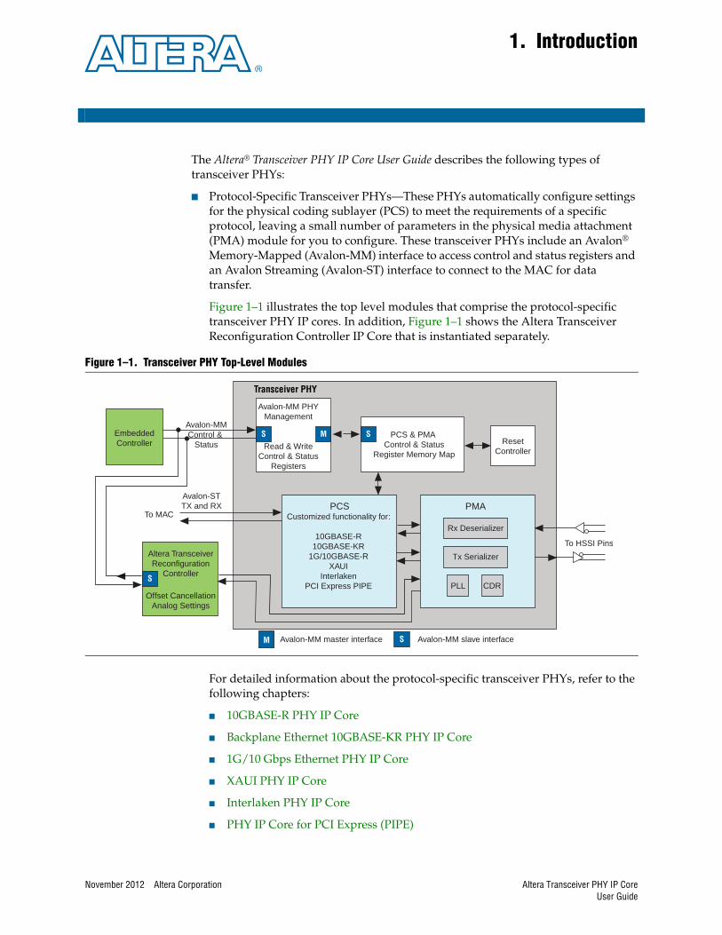
■ Protocol-Specific Transceiver PHYs—These PHYs automatically configure settings for the physical coding sublayer (PCS) to meet the requirements of a specific protocol, leaving a small number of parameters in the physical media attachment (PMA) module for you to configure. These transceiver PHYs include an Avalon® Memory-Mapped (Avalon-MM) interface to access control and status registers and an Avalon Streaming (Avalon-ST) interface to connect to the MAC for data transfer.
Figure 1–1 illustrates the top level modules that comprise the protocol-specific transceiver PHY IP cores. In addition, Figure 1–1 shows the Altera Transceiver Reconfiguration Controller IP Core that is instantiated separately.
For detailed information about the protocol-specific transceiver PHYs, refer to the following chapters:
■ 10GBASE-R PHY IP Core
■ Backplane Ethernet 10GBASE-KR PHY IP Core
■ 1G/10 Gbps Ethernet PHY IP Core
■ XAUI PHY IP Core
■ Interlaken PHY IP Core
■ PHY IP Core for PCI Express (PIPE)
Figure 1–1. Transceiver PHY Top-Level Modules
To MAC
To HSSI Pins
Transceiver PHY
PMA PCSCustomized functionality for:
10GBASE-R10GBASE-KR
1G/10GBASE-RXAUI
InterlakenPCI Express PIPE
Avalon-STTX and RX
Avalon-MMControl &
StatusPCS & PMA
Control & StatusRegister Memory Map
SReset
Controller
S
Altera TransceiverReconfiguration
Controller
Offset CancellationAnalog Settings
Avalon-MM PHYManagement
Read & WriteControl & Status
Registers
M
Avalon-MM master interfaceM
S
Avalon-MM slave interfaceS
PLL CDR
Rx Deserializer
Tx Serializer
EmbeddedController
Altera Transceiver PHY IP CoreUser Guide
1–2 Chapter 1: Introduction
■ Native Transceiver PHYs—These PHYs provide complete access to the low-level PCS and PMA hardware, allowing you to customize the transceiver settings to meet your requirements. Depending on protocol mode selected, built-in rules validate the options you select.
Figure 1–2 illustrates the Native PHY IP Core for the Stratix V device.
Figure 1–2 shows that the Stratix V Native PHY connects to the separately instantiated Transceiver Reconfiguration Controller and Transceiver PHY Reset Controller.
Table 1–1 shows the datapaths available in the Native Transceiver PHYs for Stratix V, Arria V, Arria V GZ, and Cyclone V devices.
Figure 1–2. Stratix V Transceiver Native PHY IP Core
PLLsPMA
altera_xcvr_native_<dev>Transceiver Native PHY
TransceiverReconfiguration
Controller
Reconfiguration to XCVR
Reconfiguration from XCVR
TX and RX Resets
Calilbration Busy
PLL and RX Locked
RX PCS Parallel Data
TX PCS Parallel Data
CDR Reference Clock
(when neither PCS is enabled)
TX PLL Reference Clock
Serializer/Clock
GenerationBlock
RX Serial Data
to FPGA fabric
TransceiverPHY ResetController
TX PMA Parallel Data
RX PMA Parallel Data
TX Serial DataSerializer
Deserializer
StandardPCS
(optional)
10G PCS(optional)
Table 1–1. Native PHY Datapath Availability
Datapaths Stratix V Arria V Arria V GZ Cyclone V
PMA Direct: This datapath connects the FPGA fabric directly to the PMA, minimizing latency. You must implement any required PCS functions in the FPGA fabric.
v v v —
Standard: This datapath provides a complete PCS and PMA for the TX and RX channels. You can customize the Standard datapath by enabling or disabling individual modules and specifying data widths.
v v v v
10G: This is a high performance datapath. It provides a complete PCS and PMA for the TX and RX channels. You can customize the 10G datapath by enabling or disabling individual modules and specifying data widths.
v — v —
Altera Transceiver PHY IP Core November 2012 Altera CorporationUser Guide
Chapter 1: Introduction 1–3
For detailed information about these IP cores, refer to the following chapters:
■ Stratix V Transceiver Native PHY IP Core
■ Arria V Transceiver Native PHY IP Core
■ Arria V GZ Transceiver Native PHY IP Core
■ Cyclone V Transceiver Native PHY IP Core
■ Additional PHYs—These PHYs provide more flexible settings than the protocol-specific transceiver PHYs. They include an Avalon® Memory-Mapped (Avalon-MM) interface to access control and status registers and an Avalon Streaming (Avalon-ST) interface to connect to the MAC for data transfer.
■ Custom PHY IP Core
■ Low Latency PHY IP Core
■ Deterministic Latency PHY IP Core
The following sections provide a brief introduction to the modules included in the transceiver PHYs and the separately instantiated Transceiver Reconfiguration Controller and Transceiver PHY Reset Controller IP Cores.
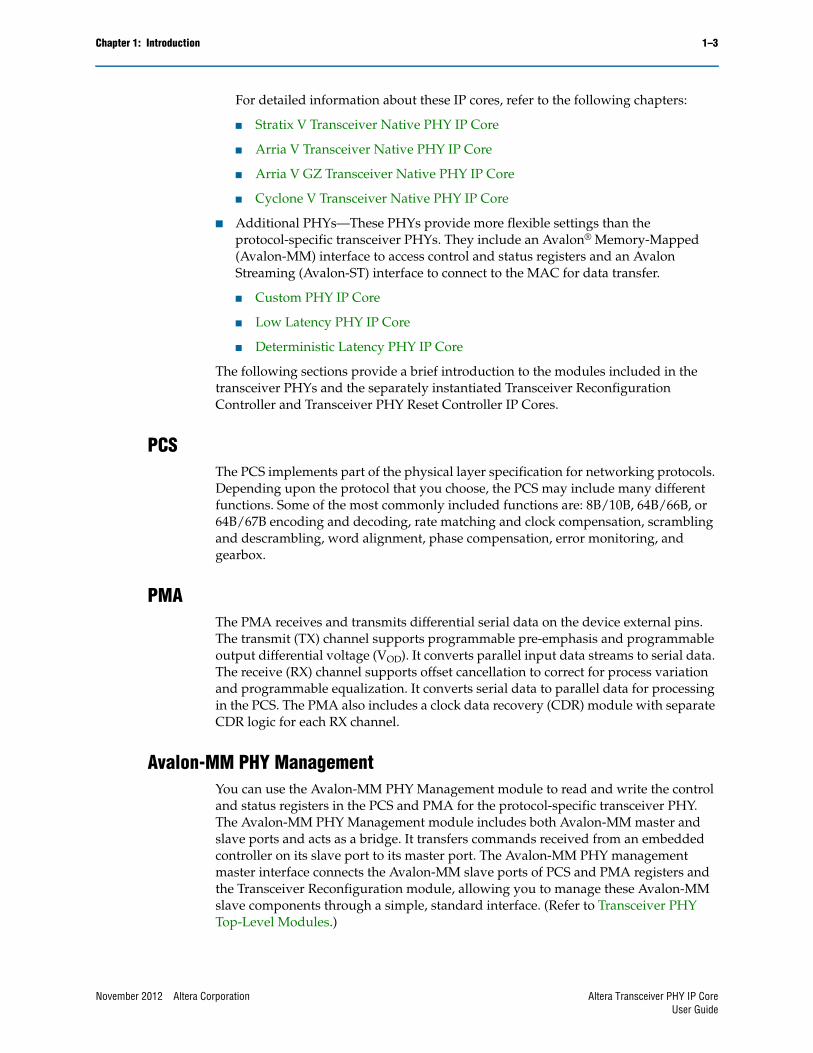
PCSThe PCS implements part of the physical layer specification for networking protocols. Depending upon the protocol that you choose, the PCS may include many different functions. Some of the most commonly included functions are: 8B/10B, 64B/66B, or 64B/67B encoding and decoding, rate matching and clock compensation, scrambling and descrambling, word alignment, phase compensation, error monitoring, and gearbox.
PMAThe PMA receives and transmits differential serial data on the device external pins. The transmit (TX) channel supports programmable pre-emphasis and programmable output differential voltage (VOD). It converts parallel input data streams to serial data. The receive (RX) channel supports offset cancellation to correct for process variation and programmable equalization. It converts serial data to parallel data for processing in the PCS. The PMA also includes a clock data recovery (CDR) module with separate CDR logic for each RX channel.
Avalon-MM PHY ManagementYou can use the Avalon-MM PHY Management module to read and write the control and status registers in the PCS and PMA for the protocol-specific transceiver PHY. The Avalon-MM PHY Management module includes both Avalon-MM master and slave ports and acts as a bridge. It transfers commands received from an embedded controller on its slave port to its master port. The Avalon-MM PHY management master interface connects the Avalon-MM slave ports of PCS and PMA registers and the Transceiver Reconfiguration module, allowing you to manage these Avalon-MM slave components through a simple, standard interface. (Refer to Transceiver PHY Top-Level Modules.)
November 2012 Altera Corporation Altera Transceiver PHY IP CoreUser Guide
1–4 Chapter 1: Introduction
Transceiver Reconfiguration ControllerAltera Transceiver Reconfiguration Controller dynamically reconfigures analog settings in Arria V, Cyclone V, and Stratix V devices. Reconfiguration allows you to compensate for variations due to process, voltage, and temperature (PVT) in 28-nm devices. It is required for Arria V, Cyclone V, and Stratix V devices that include transceivers. For more information about the Transceiver Reconfiguration Controller, refer to Transceiver Reconfiguration Controller IP Core. The reset controller may be included in the transceiver PHY as Figure 1–1 illustrates or be a separately instantiated component as Figure 1–2 illustrates.
Transceiver PHY Reset Controller The embedded reset controller ensures reliable transceiver link initialization. The reset controller initializes both the TX and RX channels. You can disable the automatic reset controller in the Custom, Low Latency Transceiver, and Deterministic Latency PHYs. If you disable the embedded reset controller, the powerdown, analog and digital reset signals for both the TX and RX channels are top-level ports of the transceiver PHY. You can use these ports to design a custom reset sequence, or you can use the Altera-provided Transceiver Reset Controller IP Core.
The Transceiver PHY Reset Controller IP Core handles all reset sequencing of the transceiver to enable successful operation. Because the Transceiver PHY Reset Controller IP is available in clear text, you can also modify it to meet your requirements. For more information about the Transceiver PHY Reset Controller, refer to Transceiver Reconfiguration Controller IP Core.
1 To accommodate different reset requirements for different transceivers in your design, instantiate multiple instances of a PHY IP core. For example, if your design includes 20 channels of the Custom PHY IP core with 12 channels running a custom protocol using the automatic reset controller and 8 channels requiring manual control of RX reset, instantiate 2 instances of the Custom PHY IP core and customize one to use automatic mode and the other to use your own reset logic. For more information, refer to “Enable embedded reset control” in Custom PHY General Options.
f For more information about reset control in Stratix V devices, refer to Transceiver Reset Control in Stratix V Devices in volume 3 of the Stratix V Device Handbook. For Stratix IV devices, refer to Reset Control and Power Down in volume 4 of the Stratix IV Device Handbook. For Arria V devices, refer to Transceiver Reset Control and Power-Down in Arria V Devices. For Cyclone V devices refer to Transceiver Reset Control and Power Down in Cyclone V Devices.
Altera Transceiver PHY IP Core November 2012 Altera CorporationUser Guide
Chapter 1: Introduction 1–5Running a Simulation Testbench
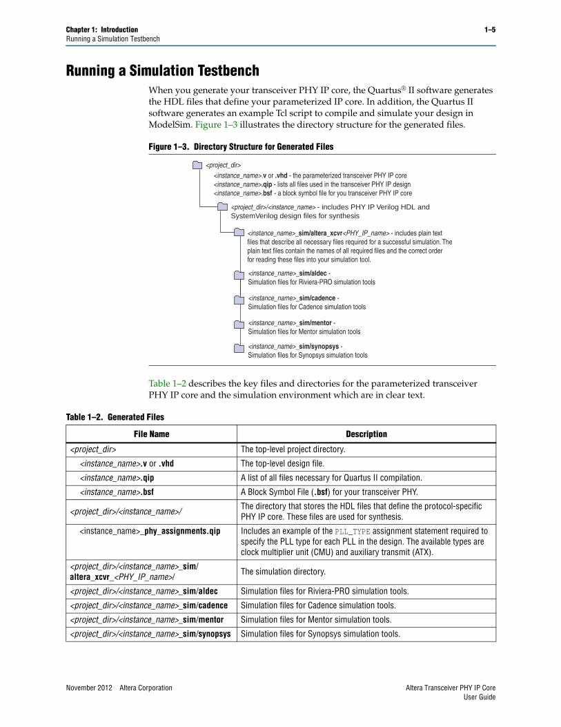
Running a Simulation Testbench When you generate your transceiver PHY IP core, the Quartus® II software generates the HDL files that define your parameterized IP core. In addition, the Quartus II software generates an example Tcl script to compile and simulate your design in ModelSim. Figure 1–3 illustrates the directory structure for the generated files.
Table 1–2 describes the key files and directories for the parameterized transceiver PHY IP core and the simulation environment which are in clear text.
Figure 1–3. Directory Structure for Generated Files
<instance_name>_sim/synopsys - Simulation files for Synopsys simulation tools
<project_dir>
<project_dir>/<instance_name> - includes PHY IP Verilog HDL andSystemVerilog design files for synthesis
<instance_name>.v or .vhd - the parameterized transceiver PHY IP core<instance_name>.qip - lists all files used in the transceiver PHY IP design<instance_name>.bsf - a block symbol file for you transceiver PHY IP core
<instance_name>_sim/altera_xcvr<PHY_IP_name> - includes plain text files that describe all necessary files required for a successful simulation. Theplain text files contain the names of all required files and the correct orderfor reading these files into your simulation tool.
<instance_name>_sim/aldec - Simulation files for Riviera-PRO simulation tools
<instance_name>_sim/cadence - Simulation files for Cadence simulation tools
<instance_name>_sim/mentor - Simulation files for Mentor simulation tools
Table 1–2. Generated Files
File Name Description
<project_dir> The top-level project directory.
<instance_name>.v or .vhd The top-level design file.
<instance_name>.qip A list of all files necessary for Quartus II compilation.
<instance_name>.bsf A Block Symbol File (.bsf) for your transceiver PHY.
<project_dir>/<instance_name>/ The directory that stores the HDL files that define the protocol-specific PHY IP core. These files are used for synthesis.
<instance_name>_phy_assignments.qip Includes an example of the PLL_TYPE assignment statement required to specify the PLL type for each PLL in the design. The available types are clock multiplier unit (CMU) and auxiliary transmit (ATX).
<project_dir>/<instance_name>_sim/altera_xcvr_<PHY_IP_name>/ The simulation directory.
<project_dir>/<instance_name>_sim/aldec Simulation files for Riviera-PRO simulation tools.
<project_dir>/<instance_name>_sim/cadence Simulation files for Cadence simulation tools.
<project_dir>/<instance_name>_sim/mentor Simulation files for Mentor simulation tools.
<project_dir>/<instance_name>_sim/synopsys Simulation files for Synopsys simulation tools.
November 2012 Altera Corporation Altera Transceiver PHY IP CoreUser Guide
1–6 Chapter 1: IntroductionUnsupported Features
The Verilog and VHDL transceiver PHY IP cores have been tested with the following simulators:
■ ModelSim SE
■ Synopsys VCS MX
■ Cadence NCSim
If you select VHDL for your transceiver PHY, only the wrapper generated by the Quartus II software is in VHDL. All the underlying files are written in Verilog or System Verilog. To enable simulation using a VHDL-only ModelSim license, the underlying Verilog and System Verilog files for the transceiver PHY are encrypted so that they can be used with the top-level VHDL wrapper without using a mixed-language simulator.
f For more information about simulating with ModelSim, refer to the Mentor Graphics ModelSim Support chapter in volume 3 of the Quartus II Handbook.
1 The transceiver PHY IP cores do not support the NativeLink feature in the Quartus II software.
Unsupported FeaturesThe protocol-specific and native transceiver PHYs are not supported in SOPC Builder or Qsys in the current release.
Altera Transceiver PHY IP Core November 2012 Altera CorporationUser Guide
November 2012 Altera Corporation
2. Getting Started
This chapter provides a general overview of the Altera IP core design flow to help you quickly get started with any Altera IP core. The Altera IP Library is installed as part of the Quartus II installation process. You can select and parameterize any Altera IP core from the library. Altera provides an integrated parameter editor that allows you to customize IP cores to support a wide variety of applications. The parameter editor guides you through the setting of parameter values and selection of optional ports. The following sections describe the general design flow and use of Altera IP cores.
Installation and LicensingThe Altera IP Library is distributed with the Quartus II software and downloadable from the Altera website (www.altera.com).
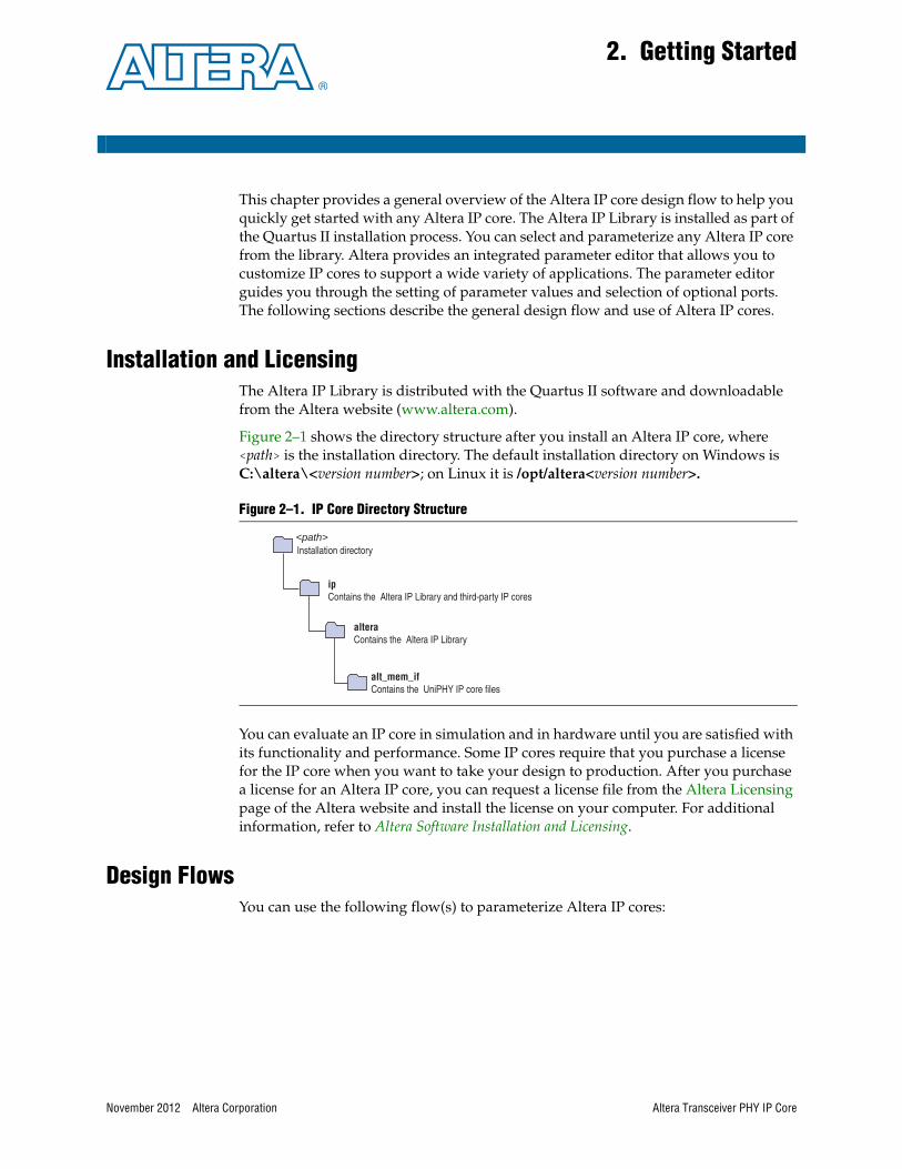
Figure 2–1 shows the directory structure after you install an Altera IP core, where <path> is the installation directory. The default installation directory on Windows is C:\altera\<version number>; on Linux it is /opt/altera<version number>.
You can evaluate an IP core in simulation and in hardware until you are satisfied with its functionality and performance. Some IP cores require that you purchase a license for the IP core when you want to take your design to production. After you purchase a license for an Altera IP core, you can request a license file from the Altera Licensing page of the Altera website and install the license on your computer. For additional information, refer to Altera Software Installation and Licensing.
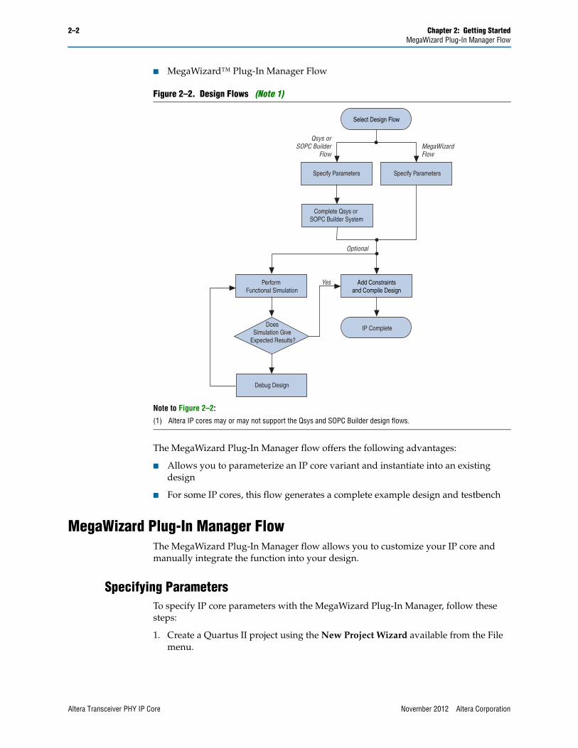
Design FlowsYou can use the following flow(s) to parameterize Altera IP cores:
Figure 2–1. IP Core Directory Structure
<path>Installation directory
ipContains the Altera IP Library and third-party IP cores
alteraContains the Altera IP Library
alt_mem_ifContains the UniPHY IP core files
Altera Transceiver PHY IP Core
2–2 Chapter 2: Getting StartedMegaWizard Plug-In Manager Flow
■ MegaWizard™ Plug-In Manager Flow
The MegaWizard Plug-In Manager flow offers the following advantages:
■ Allows you to parameterize an IP core variant and instantiate into an existing design
■ For some IP cores, this flow generates a complete example design and testbench
MegaWizard Plug-In Manager FlowThe MegaWizard Plug-In Manager flow allows you to customize your IP core and manually integrate the function into your design.
Specifying ParametersTo specify IP core parameters with the MegaWizard Plug-In Manager, follow these steps:
1. Create a Quartus II project using the New Project Wizard available from the File menu.
Figure 2–2. Design Flows (Note 1)
Note to Figure 2–2:
(1) Altera IP cores may or may not support the Qsys and SOPC Builder design flows.
Select Design Flow
Specify Parameters
Qsys orSOPC Builder
FlowMegaWizardFlow
Complete Qsys or SOPC Builder System
Specify Parameters
IP Complete
Perform Functional Simulation
Debug Design
Does Simulation Give
Expected Results?
Yes
Optional
Add Constraintsand Compile Design
Altera Transceiver PHY IP Core November 2012 Altera Corporation
Chapter 2: Getting Started 2–3MegaWizard Plug-In Manager Flow
2. In the Quartus II software, launch the MegaWizard Plug-in Manager from the Tools menu, and follow the prompts in the MegaWizard Plug-In Manager interface to create or edit a custom IP core variation.
3. To select a specific Altera IP core, click the IP core in the Installed Plug-Ins list in the MegaWizard Plug-In Manager.
4. Specify the parameters on the Parameter Settings pages. For detailed explanations of these parameters, refer to the “Parameter Settings” chapter in this document or the “Documentation” button in the MegaWizard parameter editor.
1 Some IP cores provide preset parameters for specific applications. If you wish to use preset parameters, click the arrow to expand the Presets list, select the desired preset, and then click Apply. To modify preset settings, in a text editor modify the <installation directory>/ip/altera/alt_mem_if_interfaces/alt_mem_if_<memory_protocol>_emif/alt_mem_if_<memory_protocol>_mem_model.qprs file.
5. If the IP core provides a simulation model, specify appropriate options in the wizard to generate a simulation model.
1 Altera IP supports a variety of simulation models, including simulation-specific IP functional simulation models and encrypted RTL models, and plain text RTL models. These are all cycle-accurate models. The models allow for fast functional simulation of your IP core instance using industry-standard VHDL or Verilog HDL simulators. For some cores, only the plain text RTL model is generated, and you can simulate that model.
f For more information about functional simulation models for Altera IP cores, refer to Simulating Altera Designs in volume 3 of the Quartus II Handbook.
c Use the simulation models only for simulation and not for synthesis or any other purposes. Using these models for synthesis creates a nonfunctional design.
6. If the parameter editor includes EDA and Summary tabs, follow these steps:
a. Some third-party synthesis tools can use a netlist that contains the structure of an IP core but no detailed logic to optimize timing and performance of the design containing it. To use this feature if your synthesis tool and IP core support it, turn on Generate netlist.
b. On the Summary tab, if available, select the files you want to generate. A gray checkmark indicates a file that is automatically generated. All other files are optional.
1 If file selection is supported for your IP core, after you generate the core, a generation report (<variation name>.html) appears in your project directory. This file contains information about the generated files.
7. Click the Finish button, the parameter editor generates the top-level HDL code for your IP core, and a simulation directory which includes files for simulation.
November 2012 Altera Corporation Altera Transceiver PHY IP Core
2–4 Chapter 2: Getting StartedMegaWizard Plug-In Manager Flow
1 The Finish button may be unavailable until all parameterization errors listed in the messages window are corrected.
8. Click Yes if you are prompted to add the Quartus II IP File (.qip) to the current Quartus II project. You can also turn on Automatically add Quartus II IP Files to all projects.
You can now integrate your custom IP core instance in your design, simulate, and compile. While integrating your IP core instance into your design, you must make appropriate pin assignments. You can create a virtual pin to avoid making specific pin assignments for top-level signals while you are simulating and not ready to map the design to hardware.
For some IP cores, the generation process also creates complete example designs. An example design for hardware testing is located in the <variation_name>_example_design/example_project/ directory. An example design for RTL simulation is located in the <variation_name>_example_design/simulation/ directory.
1 For information about the Quartus II software, including virtual pins and the MegaWizard Plug-In Manager, refer to Quartus II Help.
Simulate the IP CoreYou can simulate your IP core variation with the functional simulation model and the testbench or example design generated with your IP core. The functional simulation model and testbench files are generated in a project subdirectory. This directory may also include scripts to compile and run the testbench.
For a complete list of models or libraries required to simulate your IP core, refer to the scripts provided with the testbench.
For more information about simulating Altera IP cores, refer to Simulating Altera Designs in volume 3 of the Quartus II Handbook.
Altera Transceiver PHY IP Core November 2012 Altera Corporation
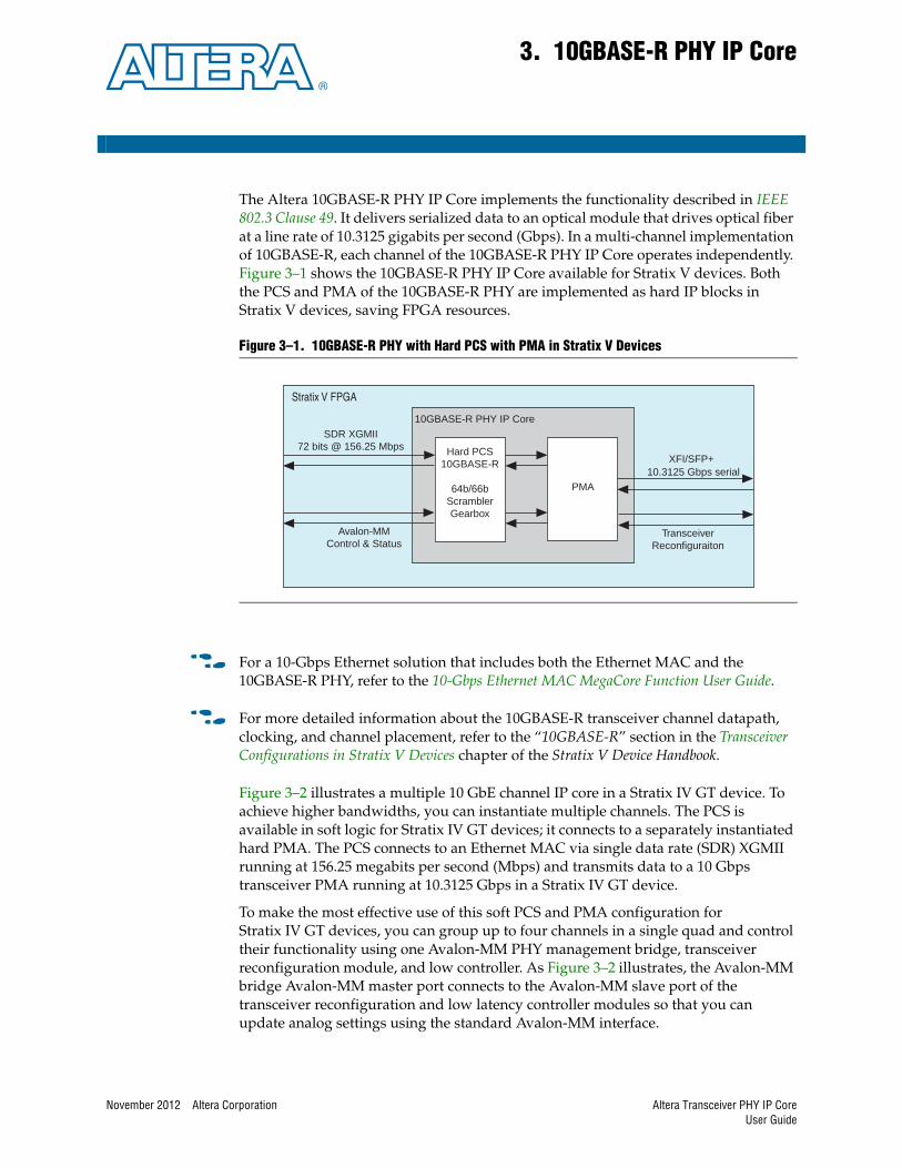
November 2012 Altera Corporation
3. 10GBASE-R PHY IP Core
The Altera 10GBASE-R PHY IP Core implements the functionality described in IEEE 802.3 Clause 49. It delivers serialized data to an optical module that drives optical fiber at a line rate of 10.3125 gigabits per second (Gbps). In a multi-channel implementation of 10GBASE-R, each channel of the 10GBASE-R PHY IP Core operates independently. Figure 3–1 shows the 10GBASE-R PHY IP Core available for Stratix V devices. Both the PCS and PMA of the 10GBASE-R PHY are implemented as hard IP blocks in Stratix V devices, saving FPGA resources.
f For a 10-Gbps Ethernet solution that includes both the Ethernet MAC and the 10GBASE-R PHY, refer to the 10-Gbps Ethernet MAC MegaCore Function User Guide.
f For more detailed information about the 10GBASE-R transceiver channel datapath, clocking, and channel placement, refer to the “10GBASE-R” section in the Transceiver Configurations in Stratix V Devices chapter of the Stratix V Device Handbook.
Figure 3–2 illustrates a multiple 10 GbE channel IP core in a Stratix IV GT device. To achieve higher bandwidths, you can instantiate multiple channels. The PCS is available in soft logic for Stratix IV GT devices; it connects to a separately instantiated hard PMA. The PCS connects to an Ethernet MAC via single data rate (SDR) XGMII running at 156.25 megabits per second (Mbps) and transmits data to a 10 Gbps transceiver PMA running at 10.3125 Gbps in a Stratix IV GT device.
To make the most effective use of this soft PCS and PMA configuration for Stratix IV GT devices, you can group up to four channels in a single quad and control their functionality using one Avalon-MM PHY management bridge, transceiver reconfiguration module, and low controller. As Figure 3–2 illustrates, the Avalon-MM bridge Avalon-MM master port connects to the Avalon-MM slave port of the transceiver reconfiguration and low latency controller modules so that you can update analog settings using the standard Avalon-MM interface.
Figure 3–1. 10GBASE-R PHY with Hard PCS with PMA in Stratix V Devices
10GBASE-R PHY IP Core
10.3125 Gbps serialXFI/SFP+
Stratix V FPGA
PMA
Hard PCS10GBASE-R
64b/66bScramblerGearbox
SDR XGMII72 bits @ 156.25 Mbps
Avalon-MMControl & Status
TransceiverReconfiguraiton
Altera Transceiver PHY IP CoreUser Guide
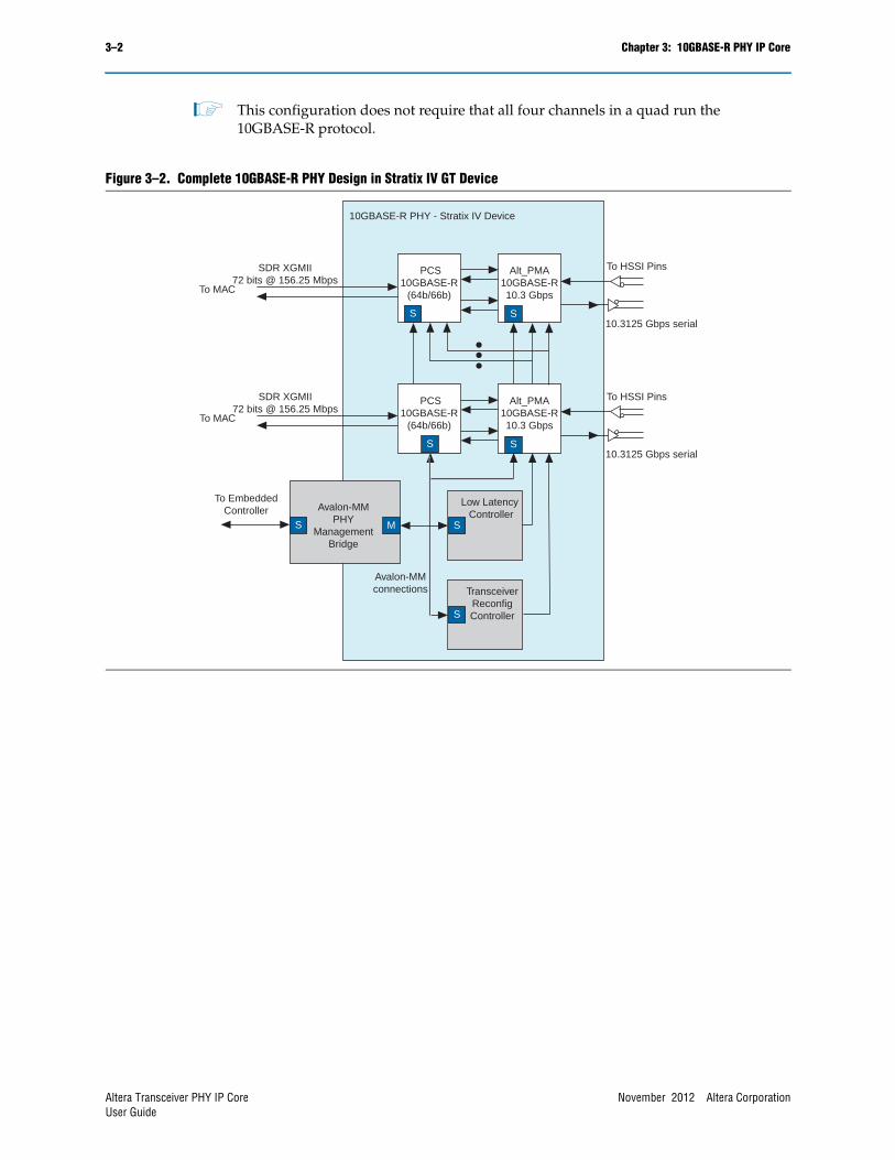
3–2 Chapter 3: 10GBASE-R PHY IP Core
1 This configuration does not require that all four channels in a quad run the 10GBASE-R protocol.
Figure 3–2. Complete 10GBASE-R PHY Design in Stratix IV GT Device
To MAC
To EmbeddedController
Avalon-MMconnections
10GBASE-R PHY - Stratix IV Device
SDR XGMII72 bits @ 156.25 Mbps
To MAC
SDR XGMII72 bits @ 156.25 Mbps
Avalon-MMPHY
ManagementBridge
MS S
Low Latency Controller
S
TransceiverReconfigController
Alt_PMA10GBASE-R10.3 Gbps
10.3125 Gbps serial
To HSSI Pins PCS10GBASE-R
(64b/66b)
S S
Alt_PMA10GBASE-R10.3 Gbps
10.3125 Gbps serial
To HSSI Pins PCS10GBASE-R
(64b/66b)
S S
Altera Transceiver PHY IP Core November 2012 Altera CorporationUser Guide
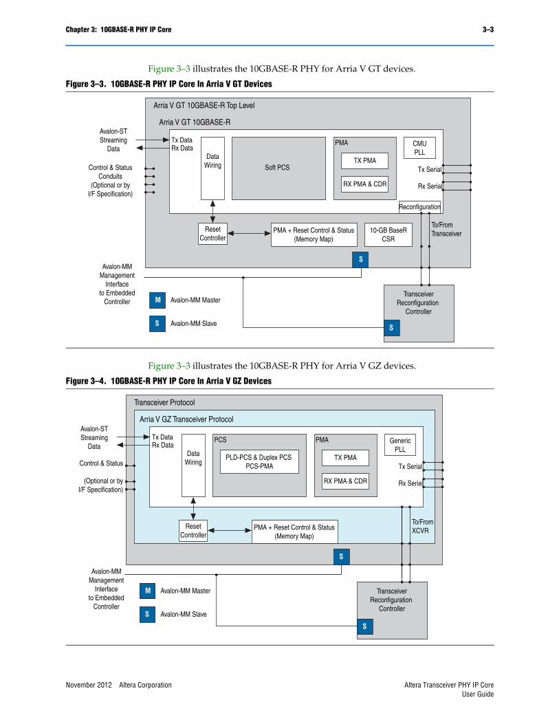
Chapter 3: 10GBASE-R PHY IP Core 3–3
Figure 3–3 illustrates the 10GBASE-R PHY for Arria V GT devices.
Figure 3–3 illustrates the 10GBASE-R PHY for Arria V GZ devices.
Figure 3–3. 10GBASE-R PHY IP Core In Arria V GT Devices
TransceiverReconfiguration
Controller
DataWiring Soft PCS
TX PMA
PMA
RX PMA & CDR
CMUPLL
ResetController
Avalon-MM Slave
Avalon-MM Master
PMA + Reset Control & Status(Memory Map)
10-GB BaseRCSR
Tx Serial
Rx Serial
Reconfiguration
Avalon-MMManagement
Interfaceto Embedded
Controller
Control & StatusConduits
(Optional or byI/F Specification)
Avalon-STStreaming
DataTx DataRx Data
Arria V GT 10GBASE-R Top Level
Arria V GT 10GBASE-R
To/FromTransceiver
S
M
S
S
Figure 3–4. 10GBASE-R PHY IP Core In Arria V GZ Devices
DataWiring
PLD-PCS & Duplex PCS PCS-PMA
PCS
TX PMA
PMA
RX PMA & CDR
GenericPLL
ResetController
TransceiverReconfiguration
Controller
S
PMA + Reset Control & Status(Memory Map)
Tx Serial
Rx Serial
S
Control & Status
(Optional or byI/F Specification)
Avalon-STStreaming
DataTx DataRx Data
Transceiver Protocol
Arria V GZ Transceiver Protocol
To/FromXCVR
Avalon-MM Slave
Avalon-MM Master
S
M
Avalon-MMManagement
Interfaceto Embedded
Controller
November 2012 Altera Corporation Altera Transceiver PHY IP CoreUser Guide
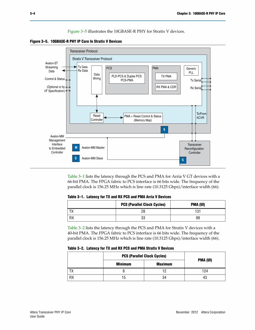
3–4 Chapter 3: 10GBASE-R PHY IP Core
Figure 3–5 illustrates the 10GBASE-R PHY for Stratix V devices.
Table 3–1 lists the latency through the PCS and PMA for Arria V GT devices with a 66-bit PMA. The FPGA fabric to PCS interface is 66 bits wide. The frequency of the parallel clock is 156.25 MHz which is line rate (10.3125 Gbps)/interface width (66).
Table 3–2 lists the latency through the PCS and PMA for Stratix V devices with a 40-bit PMA. The FPGA fabric to PCS interface is 66 bits wide. The frequency of the parallel clock is 156.25 MHz which is line rate (10.3125 Gbps)/interface width (66).
Figure 3–5. 10GBASE-R PHY IP Core In Stratix V Devices
DataWiring
PLD-PCS & Duplex PCS PCS-PMA
PCS
TX PMA
PMA
RX PMA & CDR
GenericPLL
ResetController
PMA + Reset Control & Status(Memory Map)
Tx Serial
Rx Serial
S
Control & Status
(Optional or byI/F Specification)
Avalon-STStreaming
DataTx DataRx Data
Transceiver Protocol
Stratix V Transceiver Protocol
To/FromXCVR
Avalon-MM Slave
Avalon-MM Master
S
M
Avalon-MMManagement
Interfaceto Embedded
Controller
TransceiverReconfiguration
Controller
S
Table 3–1. Latency for TX and RX PCS and PMA Arria V Devices
PCS (Parallel Clock Cycles) PMA (UI)
TX 28 131
RX 33 99
Table 3–2. Latency for TX and RX PCS and PMA Stratix V Devices
PCS (Parallel Clock Cycles)PMA (UI)
Minimum Maximum
TX 8 12 124
RX 15 34 43
Altera Transceiver PHY IP Core November 2012 Altera CorporationUser Guide
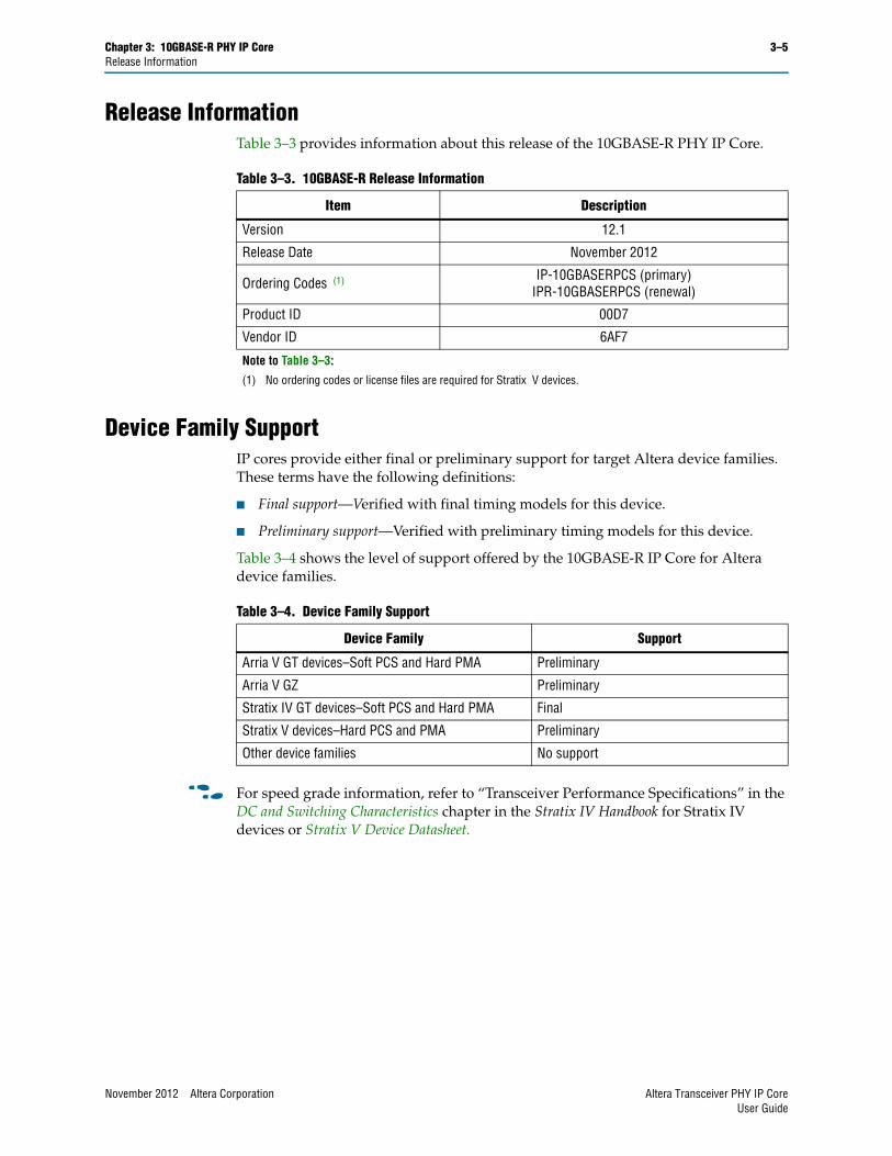
Chapter 3: 10GBASE-R PHY IP Core 3–5Release Information
Release InformationTable 3–3 provides information about this release of the 10GBASE-R PHY IP Core.
Device Family SupportIP cores provide either final or preliminary support for target Altera device families. These terms have the following definitions:
■ Final support—Verified with final timing models for this device.
■ Preliminary support—Verified with preliminary timing models for this device.
Table 3–4 shows the level of support offered by the 10GBASE-R IP Core for Altera device families.
f For speed grade information, refer to “Transceiver Performance Specifications” in the DC and Switching Characteristics chapter in the Stratix IV Handbook for Stratix IV devices or Stratix V Device Datasheet.
Table 3–3. 10GBASE-R Release Information
Item Description
Version 12.1
Release Date November 2012
Ordering Codes (1) IP-10GBASERPCS (primary)IPR-10GBASERPCS (renewal)
Product ID 00D7
Vendor ID 6AF7
Note to Table 3–3:
(1) No ordering codes or license files are required for Stratix V devices.
Table 3–4. Device Family Support
Device Family Support
Arria V GT devices–Soft PCS and Hard PMA Preliminary
Arria V GZ Preliminary
Stratix IV GT devices–Soft PCS and Hard PMA Final
Stratix V devices–Hard PCS and PMA Preliminary
Other device families No support
November 2012 Altera Corporation Altera Transceiver PHY IP CoreUser Guide
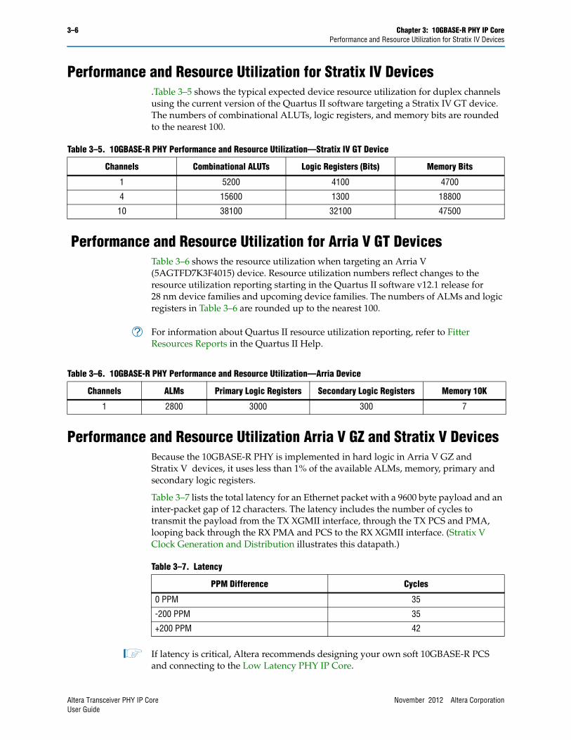
3–6 Chapter 3: 10GBASE-R PHY IP CorePerformance and Resource Utilization for Stratix IV Devices
Performance and Resource Utilization for Stratix IV Devices.Table 3–5 shows the typical expected device resource utilization for duplex channels using the current version of the Quartus II software targeting a Stratix IV GT device. The numbers of combinational ALUTs, logic registers, and memory bits are rounded to the nearest 100.
Performance and Resource Utilization for Arria V GT DevicesTable 3–6 shows the resource utilization when targeting an Arria V (5AGTFD7K3F4015) device. Resource utilization numbers reflect changes to the resource utilization reporting starting in the Quartus II software v12.1 release for 28 nm device families and upcoming device families. The numbers of ALMs and logic registers in Table 3–6 are rounded up to the nearest 100.
h For information about Quartus II resource utilization reporting, refer to Fitter Resources Reports in the Quartus II Help.
Performance and Resource Utilization Arria V GZ and Stratix V DevicesBecause the 10GBASE-R PHY is implemented in hard logic in Arria V GZ and Stratix V devices, it uses less than 1% of the available ALMs, memory, primary and secondary logic registers.
Table 3–7 lists the total latency for an Ethernet packet with a 9600 byte payload and an inter-packet gap of 12 characters. The latency includes the number of cycles to transmit the payload from the TX XGMII interface, through the TX PCS and PMA, looping back through the RX PMA and PCS to the RX XGMII interface. (Stratix V Clock Generation and Distribution illustrates this datapath.)
1 If latency is critical, Altera recommends designing your own soft 10GBASE-R PCS and connecting to the Low Latency PHY IP Core.
Table 3–5. 10GBASE-R PHY Performance and Resource Utilization—Stratix IV GT Device
Channels Combinational ALUTs Logic Registers (Bits) Memory Bits
1 5200 4100 4700
4 15600 1300 18800
10 38100 32100 47500
Table 3–6. 10GBASE-R PHY Performance and Resource Utilization—Arria Device
Channels ALMs Primary Logic Registers Secondary Logic Registers Memory 10K
1 2800 3000 300 7
Table 3–7. Latency
PPM Difference Cycles
0 PPM 35
-200 PPM 35
+200 PPM 42
Altera Transceiver PHY IP Core November 2012 Altera CorporationUser Guide
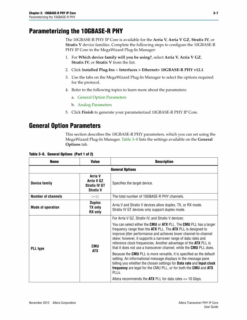
Chapter 3: 10GBASE-R PHY IP Core 3–7Parameterizing the 10GBASE-R PHY
Parameterizing the 10GBASE-R PHYThe 10GBASE-R PHY IP Core is available for the Arria V, Arria V GZ, Stratix IV, or Stratix V device families. Complete the following steps to configure the 10GBASE-R PHY IP Core in the MegaWizard Plug-In Manager:
1. For Which device family will you be using?, select Arria V, Arria V GZ, Stratix IV, or Stratix V from the list.
2. Click Installed Plug-Ins > Interfaces > Ethernet> 10GBASE-R PHY v12.1.
3. Use the tabs on the MegaWizard Plug-In Manager to select the options required for the protocol.
4. Refer to the following topics to learn more about the parameters:
a. General Option Parameters
b. Analog Parameters
5. Click Finish to generate your parameterized 10GBASE-R PHY IP Core.
General Option ParametersThis section describes the 10GBASE-R PHY parameters, which you can set using the MegaWizard Plug-In Manager. Table 3–8 lists the settings available on the General Options tab.
Table 3–8. General Options (Part 1 of 2)
Name Value Description
General Options
Device family
Arria VArria V GZ
Stratix IV GTStratix V
Specifies the target device.
Number of channels 1–32 The total number of 10GBASE-R PHY channels.
Mode of operationDuplexTX onlyRX only
Arria V and Stratix V devices allow duplex, TX, or RX mode. Stratix IV GT devices only support duplex mode.
PLL type CMUATX
For Arria V GZ, Stratix IV, and Stratix V devices:
You can select either the CMU or ATX PLL. The CMU PLL has a larger frequency range than the ATX PLL. The ATX PLL is designed to improve jitter performance and achieves lower channel-to-channel skew; however, it supports a narrower range of data rates and reference clock frequencies. Another advantage of the ATX PLL is that it does not use a transceiver channel, while the CMU PLL does.
Because the CMU PLL is more versatile, it is specified as the default setting. An informational message displays in the message pane telling you whether the chosen settings for Data rate and Input clock frequency are legal for the CMU PLL, or for both the CMU and ATX PLLs.
Altera recommends the ATX PLL for data rates <= 10 Gbps.
November 2012 Altera Corporation Altera Transceiver PHY IP CoreUser Guide
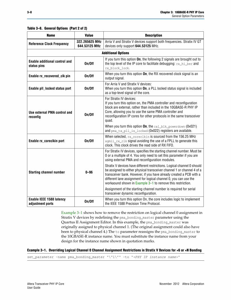
3–8 Chapter 3: 10GBASE-R PHY IP CoreGeneral Option Parameters
Example 3–1 shows how to remove the restriction on logical channel 0 assignment in Stratix V devices by redefining the pma_bonding_master parameter using the Quartus II Assignment Editor. In this example, the pma_bonding_master was originally assigned to physical channel 1. (The original assignment could also have been to physical channel 4.) The to parameter reassigns the pma_bonding_master to the 10GBASE-R instance name. You must substitute the instance name from your design for the instance name shown in quotation marks.
Reference Clock Frequency 322.265625 MHz644.53125 MHz
Arria V and Stratix V devices support both frequencies. Stratix IV GT devices only support 644.53125 MHz.
Additional Options
Enable additional control and status pins On/Off
If you turn this option On, the following 2 signals are brought out to the top level of the IP core to facilitate debugging: rx_hi_ber and rx_block_lock.
Enable rx_recovered_clk pin On/Off When you turn this option On, the RX recovered clock signal is an output signal.
Enable pll_locked status port On/OffFor Arria V and Stratix V devices:When you turn this option On, a PLL locked status signal is included as a top-level signal of the core.
Use external PMA control and reconfig On/Off
For Stratix IV devices:If you turn this option on, the PMA controller and reconfiguration block are external, rather than included in the 10GBASE-R PHY IP Core, allowing you to use the same PMA controller and reconfiguration IP cores for other protocols in the same transceiver quad.
When you turn this option On, the cal_blk_powerdown (0x021) and pma_tx_pll_is_locked (0x022) registers are available.
Enable rx_coreclkin port On/OffWhen selected, rx_coreclkin is sourced from the 156.25 MHz xgmii_rx_clk signal avoiding the use of a FPLL to generate this clock. This clock drives the read side of RX FIFO.
Starting channel number 0–96
For Stratix IV devices, specifies the starting channel number. Must be 0 or a multiple of 4. You only need to set this parameter if you are using external PMA and reconfiguration modules.
Stratix V devices have different restrictions. Logical channel 0 should be assigned to either physical transceiver channel 1 or channel 4 of a transceiver bank. However, if you have already created a PCB with a different lane assignment for logical channel 0, you can use the workaound shown in Example 3–1 to remove this restriction.
Assignment of the starting channel number is required for serial transceiver dynamic reconfiguration.
Enable IEEE 1588 latency adjustment ports On/Off When you turn this option On, the core includes logic to implement
the IEEE 1588 Precision Time Protocol.
Table 3–8. General Options (Part 2 of 2)
Name Value Description
Example 3–1. Overriding Logical Channel 0 Channel Assignment Restrictions in Stratix V Devices for ×6 or ×N Bonding
set_parameter -name pma_bonding_master "\"1\"" -to "<PHY IP instance name>"
Altera Transceiver PHY IP Core November 2012 Altera CorporationUser Guide
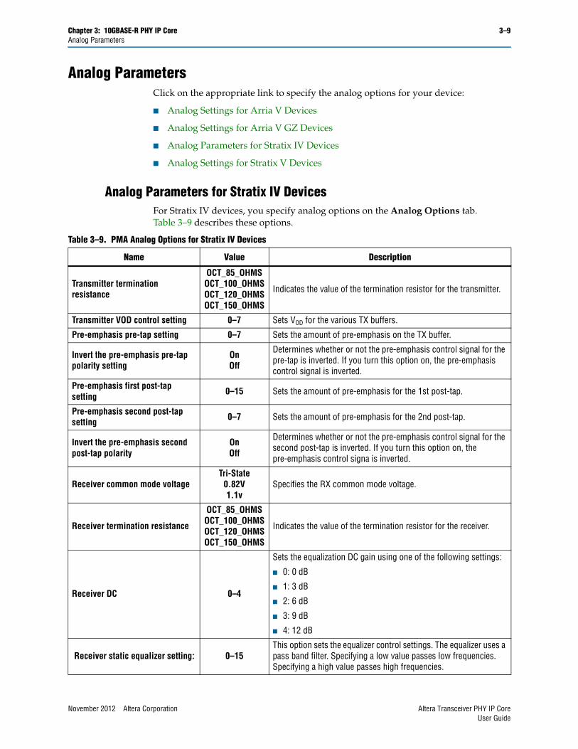
Chapter 3: 10GBASE-R PHY IP Core 3–9Analog Parameters
Analog ParametersClick on the appropriate link to specify the analog options for your device:
■ Analog Settings for Arria V Devices
■ Analog Settings for Arria V GZ Devices
■ Analog Parameters for Stratix IV Devices
■ Analog Settings for Stratix V Devices
Analog Parameters for Stratix IV DevicesFor Stratix IV devices, you specify analog options on the Analog Options tab. Table 3–9 describes these options.
Table 3–9. PMA Analog Options for Stratix IV Devices
Name Value Description
Transmitter termination resistance
OCT_85_OHMS OCT_100_OHMS OCT_120_OHMS OCT_150_OHMS
Indicates the value of the termination resistor for the transmitter.
Transmitter VOD control setting 0–7 Sets VOD for the various TX buffers.
Pre-emphasis pre-tap setting 0–7 Sets the amount of pre-emphasis on the TX buffer.
Invert the pre-emphasis pre-tap polarity setting
On Off
Determines whether or not the pre-emphasis control signal for the pre-tap is inverted. If you turn this option on, the pre-emphasis control signal is inverted.
Pre-emphasis first post-tap setting 0–15 Sets the amount of pre-emphasis for the 1st post-tap.
Pre-emphasis second post-tap setting 0–7 Sets the amount of pre-emphasis for the 2nd post-tap.
Invert the pre-emphasis second post-tap polarity
On Off
Determines whether or not the pre-emphasis control signal for the second post-tap is inverted. If you turn this option on, the pre-emphasis control signa is inverted.
Receiver common mode voltageTri-State
0.82V1.1v
Specifies the RX common mode voltage.
Receiver termination resistance
OCT_85_OHMS OCT_100_OHMS OCT_120_OHMS OCT_150_OHMS
Indicates the value of the termination resistor for the receiver.
Receiver DC 0–4
Sets the equalization DC gain using one of the following settings:
■ 0: 0 dB
■ 1: 3 dB
■ 2: 6 dB
■ 3: 9 dB
■ 4: 12 dB
Receiver static equalizer setting: 0–15This option sets the equalizer control settings. The equalizer uses a pass band filter. Specifying a low value passes low frequencies. Specifying a high value passes high frequencies.
November 2012 Altera Corporation Altera Transceiver PHY IP CoreUser Guide
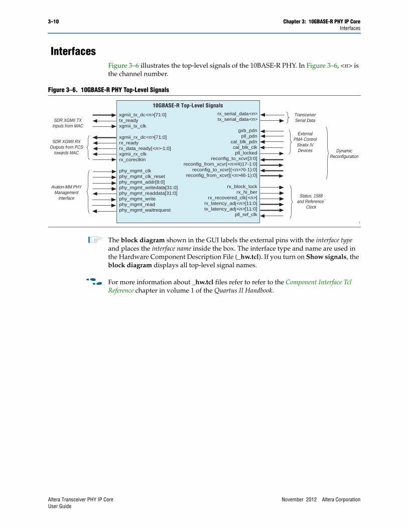
3–10 Chapter 3: 10GBASE-R PHY IP CoreInterfaces
InterfacesFigure 3–6 illustrates the top-level signals of the 10BASE-R PHY. In Figure 3–6, <n> is the channel number.
1 The block diagram shown in the GUI labels the external pins with the interface type and places the interface name inside the box. The interface type and name are used in the Hardware Component Description File (_hw.tcl). If you turn on Show signals, the block diagram displays all top-level signal names.
f For more information about _hw.tcl files refer to refer to the Component Interface Tcl Reference chapter in volume 1 of the Quartus II Handbook.
Figure 3–6. 10GBASE-R PHY Top-Level Signals
f
xgmii_tx_dc<n>[71:0]tx_readyxgmii_tx_clk
xgmii_rx_dc<n>[71:0]rx_readyrx_data_ready[<n>-1:0]xgmii_rx_clkrx_coreclkin
phy_mgmt_clkphy_mgmt_clk_resetphy_mgmt_addr[8:0]phy_mgmt_writedata[31:0]phy_mgmt_readdata[31:0]phy_mgmt_writephy_mgmt_readphy_mgmt_waitrequest
10GBASE-R Top-Level Signals
DynamicReconfiguration
ExternalPMA Control
Stratix IVDevices
rx_serial_data<n>tx_serial_data<n>
gxb_pdnpll_pdn
cal_blk_pdncal_blk_clkpll_locked
reconfig_to_xcvr[3:0]reconfig_from_xcvr[<n>/4)17-1:0]
reconfig_to_xcvr[(<n>70-1):0]reconfig_from_xcvr[(<n>46-1):0]
rx_block_lockrx_hi_ber
rx_recovered_clk[<n>]rx_latency_adj<n>[11:0]tx_latency_adj<n>[11:0]
pll_ref_clk
TransceiverSerial DataSDR XGMII TX
Inputs from MAC
SDR XGMII RXOutputs from PCS
towards MAC
Avalon-MM PHYManagement
Interface Status, 1588and Reference`
Clock
Altera Transceiver PHY IP Core November 2012 Altera CorporationUser Guide
Chapter 3: 10GBASE-R PHY IP Core 3–11Data Interfaces
Data InterfacesTable 3–10 describes the signals in the SDR XGMII TX and RX interface. The TX signals are driven from the MAC to the PCS. The RX signals are driven from the PCS to the MAC.
Table 3–10. SDR XGMII TX Inputs (Part 1 of 2)
Signal Name Direction Description
XGMII TX Interface
xgmii_tx_dc_[<n>71:0] Input
Contains 8 lanes of data and control for XGMII. Each lane consists of 8 bits of data and 1 bit of control.
■ Lane 0–[7:0]/[8]
■ Lane 1–[16:9]/[17]
■ Lane 2–[25:18]/[26]
■ Lane 3–[34:27]/[35]
■ Lane 4–[43:36]/[44]
■ Lane 5–[52:45]/[53]
■ Lane 6–[61:54]/[62]
■ Lane 7–[70:63]/[71]
Refer to Table 3–11 for the mapping of the xgmii_tx_dc data and control to the xgmii_sdr_data and xgmii_sdr_ctrl signals.
■
tx_ready OutputAsserted when the TX channel is ready to transmit data. Because the readyLatency on this Avalon-ST interface is 0, the MAC may drive tx_ready as soon as it comes out of reset.
xgmii_tx_clk Input The XGMII TX clock which runs at 156.25 MHz.
XGMII RX Interface
xgmii_rx_dc_<n>[71:0] Output
Contains 8 lanes of data and control for XGMII. Each lane consists of 8 bits of data and 1 bit of control.
■ Lane 0–[7:0]/[8]
■ Lane 1–[16:9]/[17]
■ Lane 2–[25:18]/[26]
■ Lane 3–[34:27]/[35]
■ Lane 4–[43:36]/[44]
■ Lane 5–[52:45]/[53]
■ Lane 6–[61:54]/[62]
■ Lane 7–[70:63]/[71]
Refer to Table 3–12 for the mapping of the xgmii_rx_dc data and control to the xgmii_sdr_data and xgmii_sdr_ctrl signals.
rx_ready Output Asserted when the RX reset is complete.
November 2012 Altera Corporation Altera Transceiver PHY IP CoreUser Guide
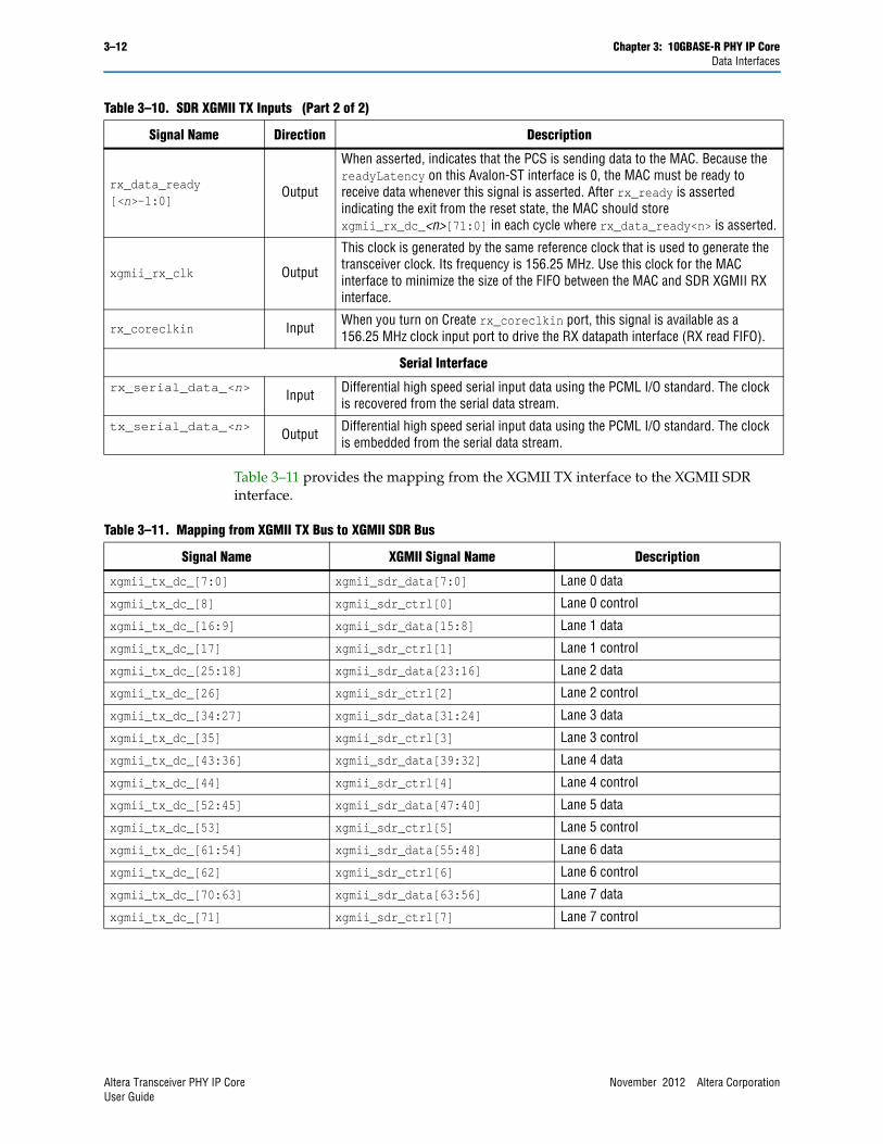
3–12 Chapter 3: 10GBASE-R PHY IP CoreData Interfaces
Table 3–11 provides the mapping from the XGMII TX interface to the XGMII SDR interface.
rx_data_ready[<n>-1:0]
Output
When asserted, indicates that the PCS is sending data to the MAC. Because the readyLatency on this Avalon-ST interface is 0, the MAC must be ready to receive data whenever this signal is asserted. After rx_ready is asserted indicating the exit from the reset state, the MAC should store xgmii_rx_dc_<n>[71:0] in each cycle where rx_data_ready<n> is asserted.
xgmii_rx_clk Output
This clock is generated by the same reference clock that is used to generate the transceiver clock. Its frequency is 156.25 MHz. Use this clock for the MAC interface to minimize the size of the FIFO between the MAC and SDR XGMII RX interface.
rx_coreclkin Input When you turn on Create rx_coreclkin port, this signal is available as a 156.25 MHz clock input port to drive the RX datapath interface (RX read FIFO).
Serial Interface
rx_serial_data_<n>Input Differential high speed serial input data using the PCML I/O standard. The clock
is recovered from the serial data stream.
tx_serial_data_<n>Output Differential high speed serial input data using the PCML I/O standard. The clock
is embedded from the serial data stream.
Table 3–10. SDR XGMII TX Inputs (Part 2 of 2)
Signal Name Direction Description
Table 3–11. Mapping from XGMII TX Bus to XGMII SDR Bus
Signal Name XGMII Signal Name Description
xgmii_tx_dc_[7:0] xgmii_sdr_data[7:0] Lane 0 data
xgmii_tx_dc_[8] xgmii_sdr_ctrl[0] Lane 0 control
xgmii_tx_dc_[16:9] xgmii_sdr_data[15:8] Lane 1 data
xgmii_tx_dc_[17] xgmii_sdr_ctrl[1] Lane 1 control
xgmii_tx_dc_[25:18] xgmii_sdr_data[23:16] Lane 2 data
xgmii_tx_dc_[26] xgmii_sdr_ctrl[2] Lane 2 control
xgmii_tx_dc_[34:27] xgmii_sdr_data[31:24] Lane 3 data
xgmii_tx_dc_[35] xgmii_sdr_ctrl[3] Lane 3 control
xgmii_tx_dc_[43:36] xgmii_sdr_data[39:32] Lane 4 data
xgmii_tx_dc_[44] xgmii_sdr_ctrl[4] Lane 4 control
xgmii_tx_dc_[52:45] xgmii_sdr_data[47:40] Lane 5 data
xgmii_tx_dc_[53] xgmii_sdr_ctrl[5] Lane 5 control
xgmii_tx_dc_[61:54] xgmii_sdr_data[55:48] Lane 6 data
xgmii_tx_dc_[62] xgmii_sdr_ctrl[6] Lane 6 control
xgmii_tx_dc_[70:63] xgmii_sdr_data[63:56] Lane 7 data
xgmii_tx_dc_[71] xgmii_sdr_ctrl[7] Lane 7 control
Altera Transceiver PHY IP Core November 2012 Altera CorporationUser Guide
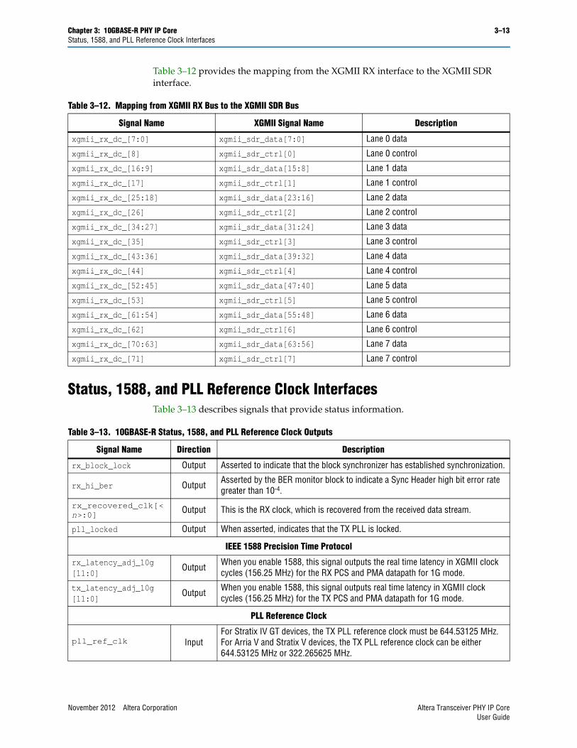
Chapter 3: 10GBASE-R PHY IP Core 3–13Status, 1588, and PLL Reference Clock Interfaces
Table 3–12 provides the mapping from the XGMII RX interface to the XGMII SDR interface.
Status, 1588, and PLL Reference Clock InterfacesTable 3–13 describes signals that provide status information.
Table 3–12. Mapping from XGMII RX Bus to the XGMII SDR Bus
Signal Name XGMII Signal Name Description
xgmii_rx_dc_[7:0] xgmii_sdr_data[7:0] Lane 0 data
xgmii_rx_dc_[8] xgmii_sdr_ctrl[0] Lane 0 control
xgmii_rx_dc_[16:9] xgmii_sdr_data[15:8] Lane 1 data
xgmii_rx_dc_[17] xgmii_sdr_ctrl[1] Lane 1 control
xgmii_rx_dc_[25:18] xgmii_sdr_data[23:16] Lane 2 data
xgmii_rx_dc_[26] xgmii_sdr_ctrl[2] Lane 2 control
xgmii_rx_dc_[34:27] xgmii_sdr_data[31:24] Lane 3 data
xgmii_rx_dc_[35] xgmii_sdr_ctrl[3] Lane 3 control
xgmii_rx_dc_[43:36] xgmii_sdr_data[39:32] Lane 4 data
xgmii_rx_dc_[44] xgmii_sdr_ctrl[4] Lane 4 control
xgmii_rx_dc_[52:45] xgmii_sdr_data[47:40] Lane 5 data
xgmii_rx_dc_[53] xgmii_sdr_ctrl[5] Lane 5 control
xgmii_rx_dc_[61:54] xgmii_sdr_data[55:48] Lane 6 data
xgmii_rx_dc_[62] xgmii_sdr_ctrl[6] Lane 6 control
xgmii_rx_dc_[70:63] xgmii_sdr_data[63:56] Lane 7 data
xgmii_rx_dc_[71] xgmii_sdr_ctrl[7] Lane 7 control
Table 3–13. 10GBASE-R Status, 1588, and PLL Reference Clock Outputs
Signal Name Direction Description
rx_block_lock Output Asserted to indicate that the block synchronizer has established synchronization.
rx_hi_ber Output Asserted by the BER monitor block to indicate a Sync Header high bit error rate greater than 10-4.
rx_recovered_clk[<n>:0]
Output This is the RX clock, which is recovered from the received data stream.
pll_locked Output When asserted, indicates that the TX PLL is locked.
IEEE 1588 Precision Time Protocol
rx_latency_adj_10g[11:0]
Output When you enable 1588, this signal outputs the real time latency in XGMII clock cycles (156.25 MHz) for the RX PCS and PMA datapath for 1G mode.
tx_latency_adj_10g[11:0]
Output When you enable 1588, this signal outputs real time latency in XGMII clock cycles (156.25 MHz) for the TX PCS and PMA datapath for 1G mode.
PLL Reference Clock
pll_ref_clk InputFor Stratix IV GT devices, the TX PLL reference clock must be 644.53125 MHz. For Arria V and Stratix V devices, the TX PLL reference clock can be either 644.53125 MHz or 322.265625 MHz.
November 2012 Altera Corporation Altera Transceiver PHY IP CoreUser Guide
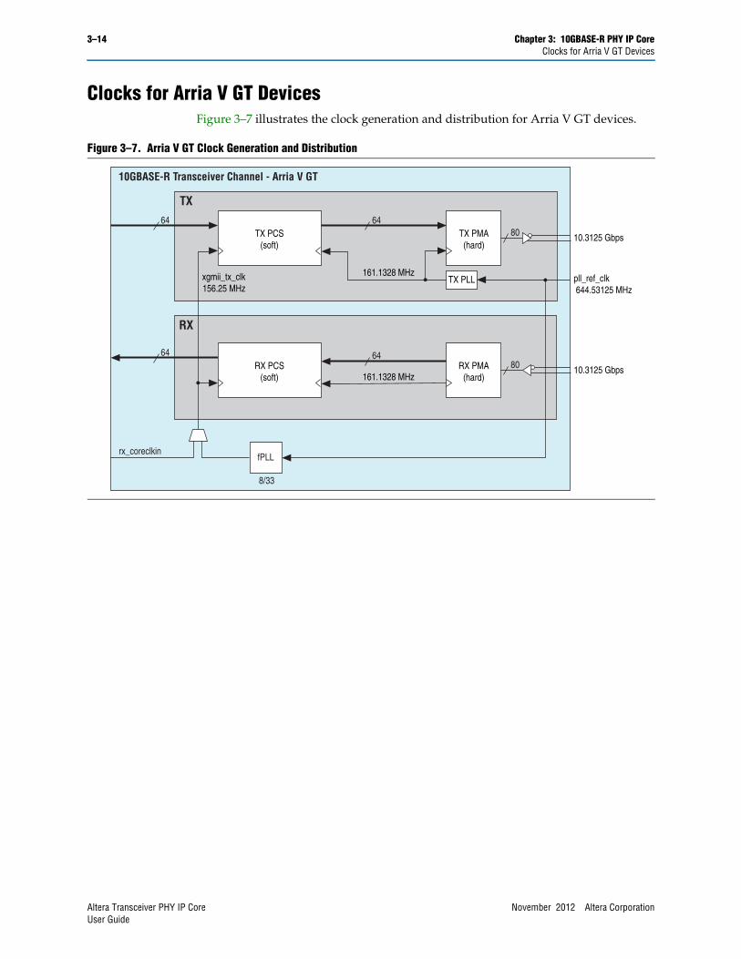
3–14 Chapter 3: 10GBASE-R PHY IP CoreClocks for Arria V GT Devices
Clocks for Arria V GT DevicesFigure 3–7 illustrates the clock generation and distribution for Arria V GT devices.
Figure 3–7. Arria V GT Clock Generation and Distribution
10GBASE-R Transceiver Channel - Arria V GT
TX PCS(soft)
RX PCS(soft)
TX PMA(hard)
RX PMA(hard)
TX PLL
64
64
64
64
80
80
xgmii_tx_clk156.25 MHz
161.1328 MHz
161.1328 MHz
10.3125 Gbps
10.3125 Gbps
pll_ref_clk 644.53125 MHz
8/33
fPLLrx_coreclkin
RX
TX
Altera Transceiver PHY IP Core November 2012 Altera CorporationUser Guide
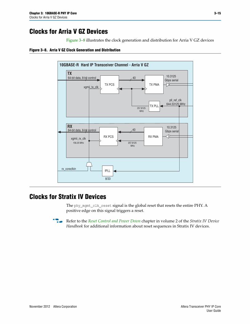
Chapter 3: 10GBASE-R PHY IP Core 3–15Clocks for Arria V GZ Devices
Clocks for Arria V GZ DevicesFigure 3–8 illustrates the clock generation and distribution for Arria V GZ devices
Clocks for Stratix IV DevicesThe phy_mgmt_clk_reset signal is the global reset that resets the entire PHY. A positive edge on this signal triggers a reset.
f Refer to the Reset Control and Power Down chapter in volume 2 of the Stratix IV Device Handbook for additional information about reset sequences in Stratix IV devices.
Figure 3–8. Arria V GZ Clock Generation and Distribution
pll_ref_clk 644.53125 MHz
10.3125 Gbps serial
257.8125 MHz
257.8125 MHz
156.25 MHz
10GBASE-R Hard IP Transceiver Channel - Arria V GZ
TX
RX
TX PCS
40
TX PMA
10.3125 Gbps serial
RX PCS
40
RX PMA
TX PLL
8/33
fPLL
xgmii_rx_clk
rx_coreclkin
xgmii_tx_clk
64-bit data, 8-bit control
64-bit data, 8-bit control
November 2012 Altera Corporation Altera Transceiver PHY IP CoreUser Guide
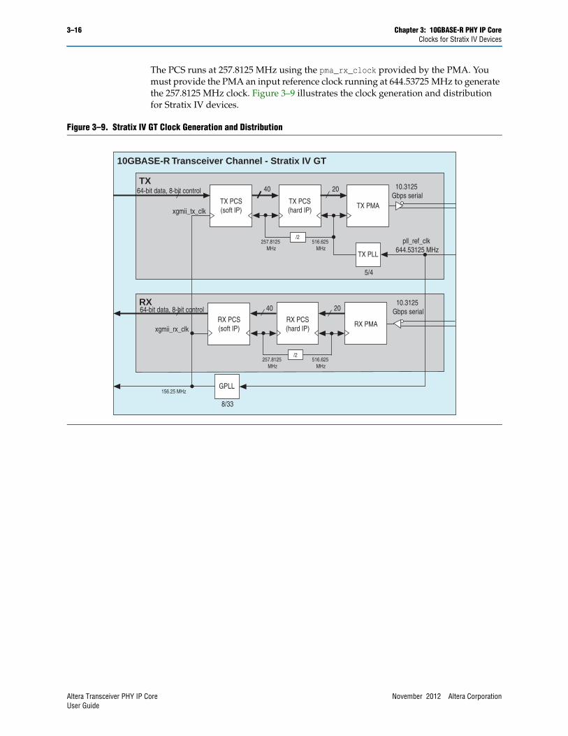
3–16 Chapter 3: 10GBASE-R PHY IP CoreClocks for Stratix IV Devices
The PCS runs at 257.8125 MHz using the pma_rx_clock provided by the PMA. You must provide the PMA an input reference clock running at 644.53725 MHz to generate the 257.8125 MHz clock. Figure 3–9 illustrates the clock generation and distribution for Stratix IV devices.
Figure 3–9. Stratix IV GT Clock Generation and Distribution
pll_ref_clk 644.53125 MHz
10.3125 Gbps serial
516.625 MHz
257.8125 MHz
516.625 MHz
257.8125 MHz
156.25 MHz
10GBASE-R Transceiver Channel - Stratix IV GT
TX
RX
TX PCS(hard IP)
TX PCS(soft IP)
204064-bit data, 8-bit control
64-bit data, 8-bit control
TX PMA
/2
10.3125 Gbps serial
RX PCS(hard IP)
RX PCS(soft IP)
2040
RX PMA
/2
5/4
TX PLL
8/33
GPLL
xgmii_rx_clk
xgmii_tx_clk
Altera Transceiver PHY IP Core November 2012 Altera CorporationUser Guide
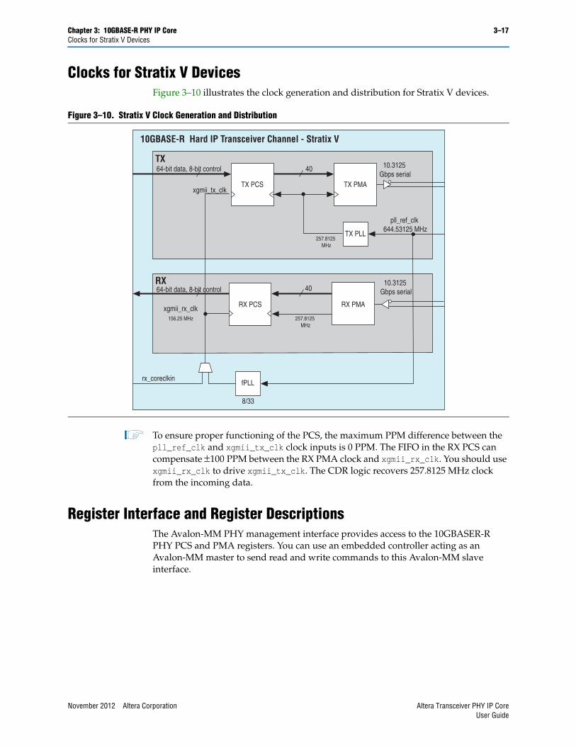
Chapter 3: 10GBASE-R PHY IP Core 3–17Clocks for Stratix V Devices
Clocks for Stratix V DevicesFigure 3–10 illustrates the clock generation and distribution for Stratix V devices.
1 To ensure proper functioning of the PCS, the maximum PPM difference between the pll_ref_clk and xgmii_tx_clk clock inputs is 0 PPM. The FIFO in the RX PCS can compensate 100 PPM between the RX PMA clock and xgmii_rx_clk. You should use xgmii_rx_clk to drive xgmii_tx_clk. The CDR logic recovers 257.8125 MHz clock from the incoming data.
Register Interface and Register DescriptionsThe Avalon-MM PHY management interface provides access to the 10GBASER-R PHY PCS and PMA registers. You can use an embedded controller acting as an Avalon-MM master to send read and write commands to this Avalon-MM slave interface.
Figure 3–10. Stratix V Clock Generation and Distribution
pll_ref_clk 644.53125 MHz
10.3125 Gbps serial
257.8125 MHz
257.8125 MHz
156.25 MHz
10GBASE-R Hard IP Transceiver Channel - Stratix V
TX
RX
TX PCS
40
TX PMA
10.3125 Gbps serial
RX PCS
40
RX PMA
TX PLL
8/33
fPLL
xgmii_rx_clk
rx_coreclkin
xgmii_tx_clk
64-bit data, 8-bit control
64-bit data, 8-bit control
November 2012 Altera Corporation Altera Transceiver PHY IP CoreUser Guide

3–18 Chapter 3: 10GBASE-R PHY IP CoreRegister Interface and Register Descriptions
Table 3–14 describes the signals that comprise the Avalon-MM PHY Management interface.
f Refer to the “Typical Slave Read and Write Transfers” and “Master Transfers” sections in the “Avalon Memory-Mapped Interfaces” chapter of the Avalon Interface Specifications for timing diagrams.
Table 3–15 specifies the registers that you can access over the Avalon-MM PHY management interface using word addresses and a 32-bit embedded processor. A single address space provides access to all registers.
1 Writing to reserved or undefined register addresses may have undefined side effects.
Table 3–14. Avalon-MM PHY Management Interface
Signal Name Direction Description
mgmt_clk Input
The clock signal that controls the Avalon-MM PHY management, interface. For Stratix IV devices, the frequency range is 37.5–50 MHz.
There is no frequency restriction for Stratix V devices; however, if you plan to use the same clock for the PHY management interface and transceiver reconfiguration, you must restrict the frequency range of mgmt_clk to 100–150 MHz to meet the specification for the transceiver reconfiguration clock.
mgmt_clk_reset Input Global reset signal that resets the entire 10GBASE-R PHY. This signal is active high and level sensitive.
mgmt_addr[7:0] Input 8-bit Avalon-MM address.
mgmt_writedata[31:0] Input Input data.
mgmt_readdata[31:0] Output Output data.
mgmt_write Input Write signal. Asserted high.
mgmt_read Input Read signal. Asserted high.
mgmt_waitrequest OutputWhen asserted, indicates that the Avalon-MM slave interface is unable to respond to a read or write request. When asserted, control signals to the Avalon-MM slave interface must remain constant.
Table 3–15. 10GBASE-R Register Descriptions (Part 1 of 3)
WordAddr Bit R/W Name Description
PMA Common Control and Status
0x021 [31:0] RW cal_blk_powerdown
Writing a 1 to channel <n> powers down the calibration block for channel <n> . This register is only available if you select Use external PMA control and reconfig on the Additional Options tab of the GUI.
0x022 [31:0] RO pma_tx_pll_is_locked
Bit[P] indicates that the TX clock multiplier unit CMU PLL [P] is locked to the input reference clock. This register is only available if you select Use external PMA control and reconfig on the Additional Options tab of the GUI.
Altera Transceiver PHY IP Core November 2012 Altera CorporationUser Guide
Chapter 3: 10GBASE-R PHY IP Core 3–19Register Interface and Register Descriptions
Reset Control Registers–Automatic Reset Controller
0x041 [31:0] RW reset_ch_bitmaskReset controller channel bitmask for digital resets. The default value is all 1 s. Channel <n> can be reset when bit<n> = 1. Channel <n> cannot be reset when bit<n>=0.
0x042 [1:0]
WO reset_control (write)
Writing a 1 to bit 0 initiates a TX digital reset using the reset controller module. The reset affects channels enabled in the reset_ch_bitmask. Writing a 1 to bit 1 initiates a RX digital reset of channels enabled in the reset_ch_bitmask. Both bits 0 and 1 self-clear.
RO reset_status (read)Reading bit 0 returns the status of the reset controller TX ready bit. Reading bit 1 returns the status of the reset controller RX ready bit.
0x044
[31:0] RW reset_fine_control
You can use the reset_fine_control register to create your own reset sequence. The reset control module, illustrated in Transceiver PHY Top-Level Modules, performs a standard reset sequence at power on and whenever the phy_mgmt_clk_reset is asserted. Bits [31:4,0] are reserved.
[31:4,0] RW Reserved It is safe to write 0s to reserved bits.
[1] RW reset_tx_digital
Writing a 1 causes the internal TX digital reset signal to be asserted, resetting all channels enabled in reset_ch_bitmask. You must write a 0 to clear the reset condition.
[2] RW reset_rx_analog
Writing a 1 causes the internal RX digital reset signal to be asserted, resetting the RX analog logic of all channels enabled in reset_ch_bitmask. You must write a 0 to clear the reset condition.
[3] RW reset_rx_digital
Writing a 1 causes the RX digital reset signal to be asserted, resetting the RX digital channels enabled in reset_ch_bitmask. You must write a 0 to clear the reset condition.
PMA Channel Control and Status
0x061 [31:0] RW phy_serial_loopbackWriting a 1 to channel <n> puts channel <n> in serial loopback mode. For information about pre- or post-CDR serial loopback modes, refer to Loopback Modes.
0x064 [31:0] RW pma_rx_set_locktodataWhen set, programs the RX CDR PLL to lock to the incoming data. Bit <n> corresponds to channel <n>.
0x065 [31:0] RW pma_rx_set_locktorefWhen set, programs the RX CDR PLL to lock to the reference clock. Bit <n> corresponds to channel <n>.
0x066 [31:0] RO pma_rx_is_lockedtodataWhen asserted, indicates that the RX CDR PLL is locked to the RX data, and that the RX CDR has changed from LTR to LTD mode. Bit <n> corresponds to channel <n>.
0x067 [31:0] RO pma_rx_is_lockedtorefWhen asserted, indicates that the RX CDR PLL is locked to the reference clock. Bit <n> corresponds to channel <n>.
Table 3–15. 10GBASE-R Register Descriptions (Part 2 of 3)
WordAddr Bit R/W Name Description
November 2012 Altera Corporation Altera Transceiver PHY IP CoreUser Guide
3–20 Chapter 3: 10GBASE-R PHY IP CoreRegister Interface and Register Descriptions
10GBASE-R PCS
0x080 [31:0] WO INDIRECT_ADDRProvides for indirect addressing of all PCS control and status registers. Use this register to specify the logical channel number of the PCS channel you want to access.
0x081
[2] RW RCLR_ERRBLK_CNTWhen set to 1, clears the error block count register.
To block: Block synchronizer
[3] RW RCLR_BER_COUNTWhen set to 1, clears the bit error rate (BER) register.
To block: BER monitor
0x082
[0] R PCS_STATUSFor Stratix IV devices:When asserted indicates that the PCS link is up.
[1] R HI_BER
When asserted by the BER monitor block, indicates that the PCS is recording a high BER.
From block: BER monitor
[2] R BLOCK_LOCK
When asserted by the block synchronizer, indicates that the PCS is locked to received blocks.
From Block: Block synchronizer
[3] R TX_FIFO_FULLWhen asserted, indicates the TX FIFO is full.
From block: TX FIFO
[4] R RX_FIFO_FULLWhen asserted, indicates the RX FIFO is full.
From block: RX FIFO
[5] R RX_SYNC_HEAD_ERRORFor Stratix V devices, when asserted, indicates an RX synchronization error. This signal is Stratix V devices only.
[6] R RX_SCRAMBLER_ERRORFor Stratix V devices:When asserted, indicates an RX scrambler error.
[7] R RX_DATA_READYWhen asserted indicates that the RX interface is ready to send out received data. From block: 10 Gbps Receiver PCS
0x083
[5:0] R BER_COUNT[5:0]For Stratix IV devices only, records the bit error rate (BER).
From block: BER monitor
[13:6] R ERROR_BLOCK_COUNT[7:0]
For Stratix IV devices only, records the number of blocks that contain errors.
From Block: Block synchronizer
Table 3–15. 10GBASE-R Register Descriptions (Part 3 of 3)
WordAddr Bit R/W Name Description
Altera Transceiver PHY IP Core November 2012 Altera CorporationUser Guide
Chapter 3: 10GBASE-R PHY IP Core 3–21Dynamic Reconfiguration for Stratix IV Devices
Dynamic Reconfiguration for Stratix IV DevicesTable 3–16 describes the additional top-level signals 10GBASE-R PHY IP Core when the configuration uses external modules for PMA control and reconfiguration. You enable this configuration by turning on Use external PMA control and reconfig available for Stratix IV GT devices.
Dynamic Reconfiguration for Arria V and Stratix V DevicesFor Arria V and Stratix V devices, each channel and each TX PLL have separate dynamic reconfiguration interfaces. The MegaWizard Plug-In Manager provides informational messages on the connectivity of these interfaces. Example 3–2 shows the messages for a single duplex channel.
Although you must initially create a separate reconfiguration interface for each channel and TX PLL in your design, when the Quartus II software compiles your design, it reduces the number of reconfiguration interfaces by merging reconfiguration interfaces. The synthesized design typically includes a reconfiguration interface for at least three channels because three channels share an Avalon-MM slave interface which connects to the Transceiver Reconfiguration Controller IP Core. Conversely, you cannot connect the three channels that share an Avalon-MM interface to different Transceiver Reconfiguration Controllers. Doing so causes a Fitter error. For more information, refer to Transceiver Reconfiguration Controller to PHY IP Connectivity. Allowing the Quartus II software to merge reconfiguration interfaces gives the Fitter more flexibility in placing transceiver channels.
Table 3–16. External PMA and Reconfiguration Signals
Signal Name Direction Description
gxb_pdnInput When asserted, powers down the entire GT block. Active high. For
Stratix IV de
pll_pdn Input When asserted, powers down the TX PLL. Active high.
cal_blk_pdn Input When asserted, powers down the calibration block. Active high.
cal_blk_clkInput
Calibration clock. For Stratix IV devices only. It must be in the range 37.5–50 MHz. You can use the same clock for the phy_mgmt_clk and the cal_blk_clk.
pll_locked Output When asserted, indicates that the TX PLL is locked.
reconfig_to_xcvr[3:0]Input Reconfiguration signals from the Transceiver Reconfiguration Controller
to the PHY device. This signal is only available in Stratix IV devices.
reconfig_from_xcvr[(<n>/4)17-1:0] Output
Reconfiguration RAM. The PHY device drives this RAM data to the transceiver reconfiguration IP. This signal is only available in Stratix IV devices.
Example 3–2. Informational Messages for the Transceiver Reconfiguration Interface
PHY IP will require 2 reconfiguration interfaces for connection to the external reconfiguration controller.Reconfiguration interface offset 0 is connected to the transceiver channel.Reconfiguration interface offset 1 is connected to the transmit PLL.
November 2012 Altera Corporation Altera Transceiver PHY IP CoreUser Guide
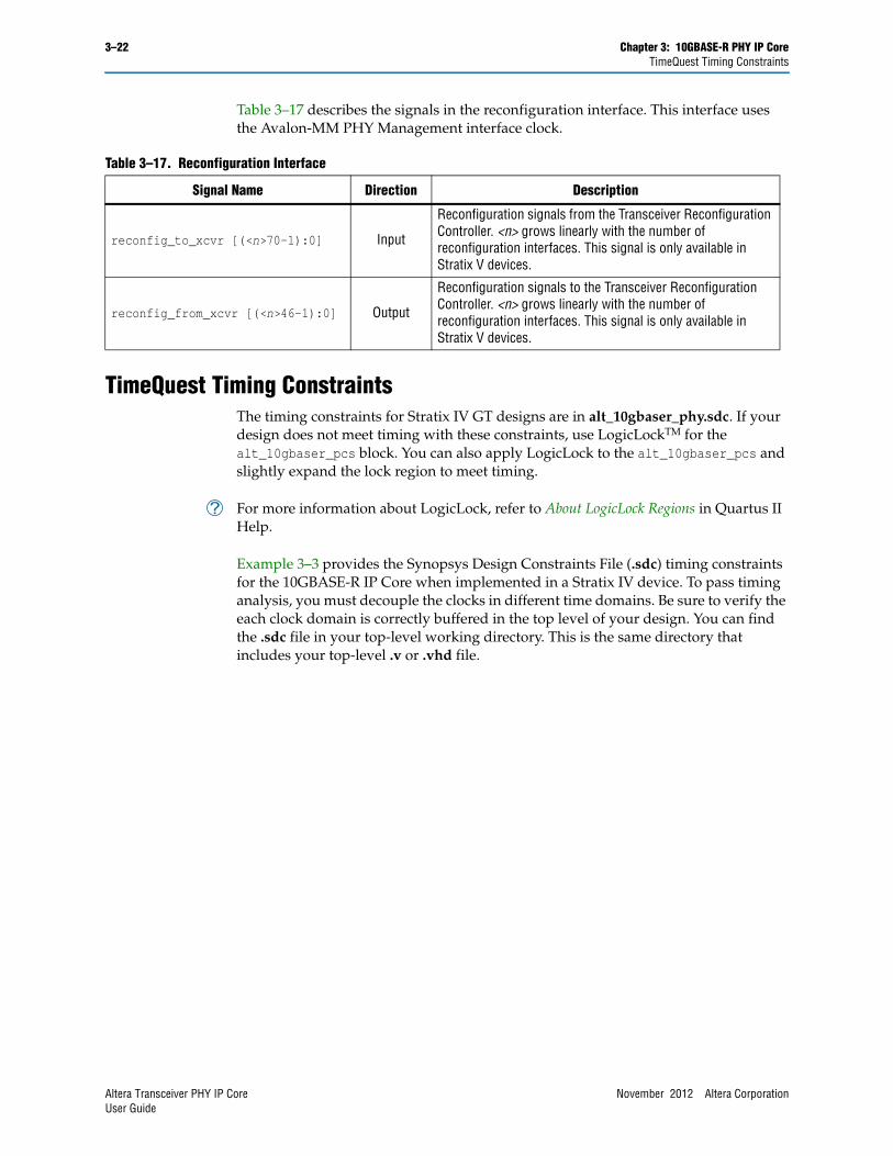
3–22 Chapter 3: 10GBASE-R PHY IP CoreTimeQuest Timing Constraints
Table 3–17 describes the signals in the reconfiguration interface. This interface uses the Avalon-MM PHY Management interface clock.
TimeQuest Timing ConstraintsThe timing constraints for Stratix IV GT designs are in alt_10gbaser_phy.sdc. If your design does not meet timing with these constraints, use LogicLockTM for the alt_10gbaser_pcs block. You can also apply LogicLock to the alt_10gbaser_pcs and slightly expand the lock region to meet timing.
h For more information about LogicLock, refer to About LogicLock Regions in Quartus II Help.
Example 3–3 provides the Synopsys Design Constraints File (.sdc) timing constraints for the 10GBASE-R IP Core when implemented in a Stratix IV device. To pass timing analysis, you must decouple the clocks in different time domains. Be sure to verify the each clock domain is correctly buffered in the top level of your design. You can find the .sdc file in your top-level working directory. This is the same directory that includes your top-level .v or .vhd file.
Table 3–17. Reconfiguration Interface
Signal Name Direction Description
reconfig_to_xcvr [(<n>70-1):0] Input
Reconfiguration signals from the Transceiver Reconfiguration Controller. <n> grows linearly with the number of reconfiguration interfaces. This signal is only available in Stratix V devices.
reconfig_from_xcvr [(<n>46-1):0] Output
Reconfiguration signals to the Transceiver Reconfiguration Controller. <n> grows linearly with the number of reconfiguration interfaces. This signal is only available in Stratix V devices.
Altera Transceiver PHY IP Core November 2012 Altera CorporationUser Guide
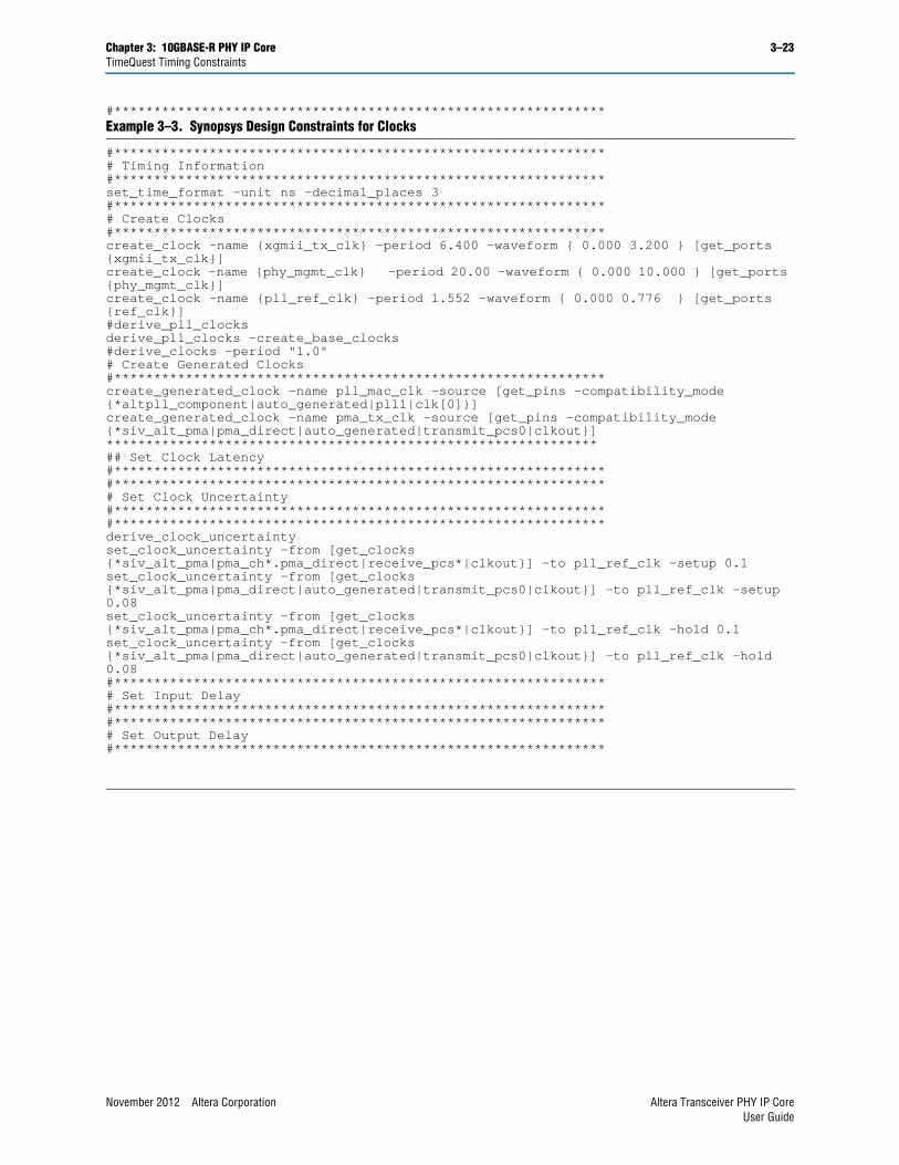
Chapter 3: 10GBASE-R PHY IP Core 3–23TimeQuest Timing Constraints
#**************************************************************Example 3–3. Synopsys Design Constraints for Clocks
#**************************************************************# Timing Information#**************************************************************set_time_format -unit ns -decimal_places 3#**************************************************************# Create Clocks#**************************************************************create_clock -name {xgmii_tx_clk} -period 6.400 -waveform { 0.000 3.200 } [get_ports {xgmii_tx_clk}]create_clock -name {phy_mgmt_clk} -period 20.00 -waveform { 0.000 10.000 } [get_ports {phy_mgmt_clk}]create_clock -name {pll_ref_clk} -period 1.552 -waveform { 0.000 0.776 } [get_ports {ref_clk}]#derive_pll_clocksderive_pll_clocks -create_base_clocks#derive_clocks -period "1.0"# Create Generated Clocks#**************************************************************create_generated_clock -name pll_mac_clk -source [get_pins -compatibility_mode {*altpll_component|auto_generated|pll1|clk[0]}] create_generated_clock -name pma_tx_clk -source [get_pins -compatibility_mode {*siv_alt_pma|pma_direct|auto_generated|transmit_pcs0|clkout}] **************************************************************## Set Clock Latency#**************************************************************#**************************************************************# Set Clock Uncertainty#**************************************************************#**************************************************************derive_clock_uncertaintyset_clock_uncertainty -from [get_clocks {*siv_alt_pma|pma_ch*.pma_direct|receive_pcs*|clkout}] -to pll_ref_clk -setup 0.1set_clock_uncertainty -from [get_clocks {*siv_alt_pma|pma_direct|auto_generated|transmit_pcs0|clkout}] -to pll_ref_clk -setup 0.08set_clock_uncertainty -from [get_clocks {*siv_alt_pma|pma_ch*.pma_direct|receive_pcs*|clkout}] -to pll_ref_clk -hold 0.1set_clock_uncertainty -from [get_clocks {*siv_alt_pma|pma_direct|auto_generated|transmit_pcs0|clkout}] -to pll_ref_clk -hold 0.08#**************************************************************# Set Input Delay#**************************************************************#**************************************************************# Set Output Delay#**************************************************************
November 2012 Altera Corporation Altera Transceiver PHY IP CoreUser Guide
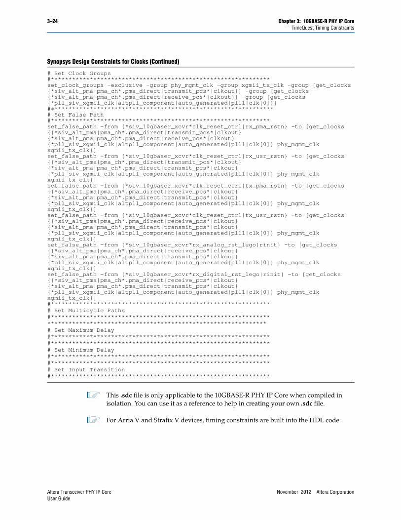
3–24 Chapter 3: 10GBASE-R PHY IP CoreTimeQuest Timing Constraints
1 This .sdc file is only applicable to the 10GBASE-R PHY IP Core when compiled in isolation. You can use it as a reference to help in creating your own .sdc file.
1 For Arria V and Stratix V devices, timing constraints are built into the HDL code.
Synopsys Design Constraints for Clocks (Continued)
# Set Clock Groups#**************************************************************set_clock_groups -exclusive -group phy_mgmt_clk -group xgmii_tx_clk -group [get_clocks {*siv_alt_pma|pma_ch*.pma_direct|transmit_pcs*|clkout}] -group [get_clocks {*siv_alt_pma|pma_ch*.pma_direct|receive_pcs*|clkout}] -group [get_clocks {*pll_siv_xgmii_clk|altpll_component|auto_generated|pll1|clk[0]}] ##**************************************************************# Set False Path#**************************************************************set_false_path -from {*siv_10gbaser_xcvr*clk_reset_ctrl|rx_pma_rstn} -to [get_clocks {{*siv_alt_pma|pma_ch*.pma_direct|transmit_pcs*|clkout} {*siv_alt_pma|pma_ch*.pma_direct|receive_pcs*|clkout} {*pll_siv_xgmii_clk|altpll_component|auto_generated|pll1|clk[0]} phy_mgmt_clk xgmii_tx_clk}]set_false_path -from {*siv_10gbaser_xcvr*clk_reset_ctrl|rx_usr_rstn} -to [get_clocks {{*siv_alt_pma|pma_ch*.pma_direct|transmit_pcs*|clkout} {*siv_alt_pma|pma_ch*.pma_direct|transmit_pcs*|clkout} {*pll_siv_xgmii_clk|altpll_component|auto_generated|pll1|clk[0]} phy_mgmt_clk xgmii_tx_clk}]set_false_path -from {*siv_10gbaser_xcvr*clk_reset_ctrl|tx_pma_rstn} -to [get_clocks {{*siv_alt_pma|pma_ch*.pma_direct|receive_pcs*|clkout} {*siv_alt_pma|pma_ch*.pma_direct|transmit_pcs*|clkout} {*pll_siv_xgmii_clk|altpll_component|auto_generated|pll1|clk[0]} phy_mgmt_clk xgmii_tx_clk}]set_false_path -from {*siv_10gbaser_xcvr*clk_reset_ctrl|tx_usr_rstn} -to [get_clocks {{*siv_alt_pma|pma_ch*.pma_direct|receive_pcs*|clkout} {*siv_alt_pma|pma_ch*.pma_direct|transmit_pcs*|clkout} {*pll_siv_xgmii_clk|altpll_component|auto_generated|pll1|clk[0]} phy_mgmt_clk xgmii_tx_clk}]set_false_path -from {*siv_10gbaser_xcvr*rx_analog_rst_lego|rinit} -to [get_clocks {{*siv_alt_pma|pma_ch*.pma_direct|receive_pcs*|clkout} {*siv_alt_pma|pma_ch*.pma_direct|transmit_pcs*|clkout} {*pll_siv_xgmii_clk|altpll_component|auto_generated|pll1|clk[0]} phy_mgmt_clk xgmii_tx_clk}]set_false_path -from {*siv_10gbaser_xcvr*rx_digital_rst_lego|rinit} -to [get_clocks {{*siv_alt_pma|pma_ch*.pma_direct|receive_pcs*|clkout} {*siv_alt_pma|pma_ch*.pma_direct|transmit_pcs*|clkout} {*pll_siv_xgmii_clk|altpll_component|auto_generated|pll1|clk[0]} phy_mgmt_clk xgmii_tx_clk}]#**************************************************************# Set Multicycle Paths#****************************************************************************************************************************# Set Maximum Delay#**************************************************************#**************************************************************# Set Minimum Delay#**************************************************************#**************************************************************# Set Input Transition#**************************************************************
Altera Transceiver PHY IP Core November 2012 Altera CorporationUser Guide

Chapter 3: 10GBASE-R PHY IP Core 3–25Simulation Files and Example Testbench
Simulation Files and Example TestbenchRefer to Running a Simulation Testbench for a description of the directories and files that the Quartus II software creates automatically when you generate your 10GBASE-R PHY IP Core.
f Refer to the Altera wiki for an example testbench that you can use as a starting point in creating your own verification environment.
November 2012 Altera Corporation Altera Transceiver PHY IP CoreUser Guide

3–26 Chapter 3: 10GBASE-R PHY IP CoreSimulation Files and Example Testbench
Altera Transceiver PHY IP Core November 2012 Altera CorporationUser Guide
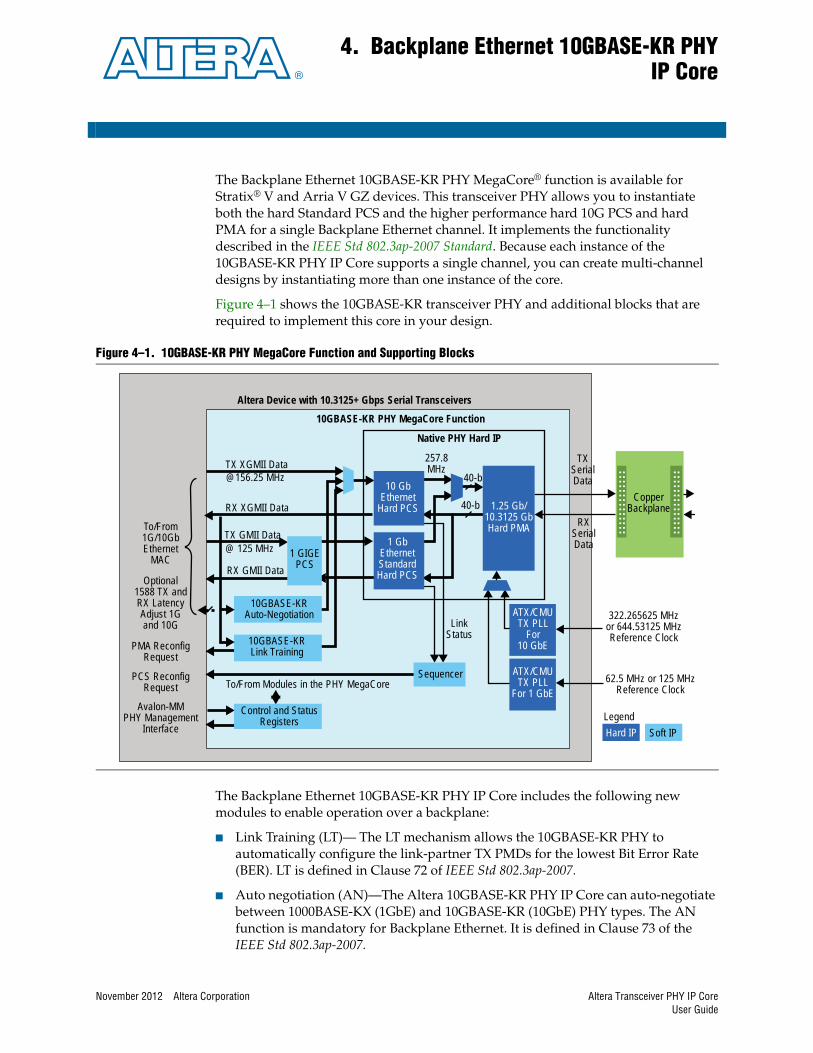
November 2012 Altera Corporation
4. Backplane Ethernet 10GBASE-KR PHYIP Core
The Backplane Ethernet 10GBASE-KR PHY MegaCore® function is available for Stratix® V and Arria V GZ devices. This transceiver PHY allows you to instantiate both the hard Standard PCS and the higher performance hard 10G PCS and hard PMA for a single Backplane Ethernet channel. It implements the functionality described in the IEEE Std 802.3ap-2007 Standard. Because each instance of the 10GBASE-KR PHY IP Core supports a single channel, you can create multi-channel designs by instantiating more than one instance of the core.
Figure 4–1 shows the 10GBASE-KR transceiver PHY and additional blocks that are required to implement this core in your design.
The Backplane Ethernet 10GBASE-KR PHY IP Core includes the following new modules to enable operation over a backplane:
■ Link Training (LT)— The LT mechanism allows the 10GBASE-KR PHY to automatically configure the link-partner TX PMDs for the lowest Bit Error Rate (BER). LT is defined in Clause 72 of IEEE Std 802.3ap-2007.
■ Auto negotiation (AN)—The Altera 10GBASE-KR PHY IP Core can auto-negotiate between 1000BASE-KX (1GbE) and 10GBASE-KR (10GbE) PHY types. The AN function is mandatory for Backplane Ethernet. It is defined in Clause 73 of the IEEE Std 802.3ap-2007.
Figure 4–1. 10GBASE-KR PHY MegaCore Function and Supporting Blocks
Altera Device with 10.3125+ Gbps Serial Transceivers10GBASE-KR PHY MegaCore Function
Native PHY Hard IP
257.8MHz
40-b
40-b
TXSerialData
RXSerialData
CopperBackplane
322.265625 MHzor 644.53125 MHzReference Clock
62.5 MHz or 125 MHzReference Clock
LegendHard IP Soft IP
ATX/CMUTX PLL
For10 GbE
ATX/CMUTX PLL
For 1 GbE
1.25 Gb/10.3125 GbHard PMA
LinkStatus
Sequencer
10 GbEthernet
Hard PCS
1 GbEthernetStandardHard PCS
To/From Modules in the PHY MegaCore
Control and StatusRegisters
Avalon-MMPHY Management
Interface
PCS ReconfigRequest
PMA ReconfigRequest
Optional1588 TX andRX LatencyAdjust 1Gand 10G
To/From1G/10GbEthernet
MACRX GMII Data
TX GMII Data@ 125 MHz
RX XGMII Data
TX XGMII [email protected] MHz
1 GIGEPCS
10GBASE-KRAuto-Negotiation
10GBASE-KRLink Training
Altera Transceiver PHY IP CoreUser Guide
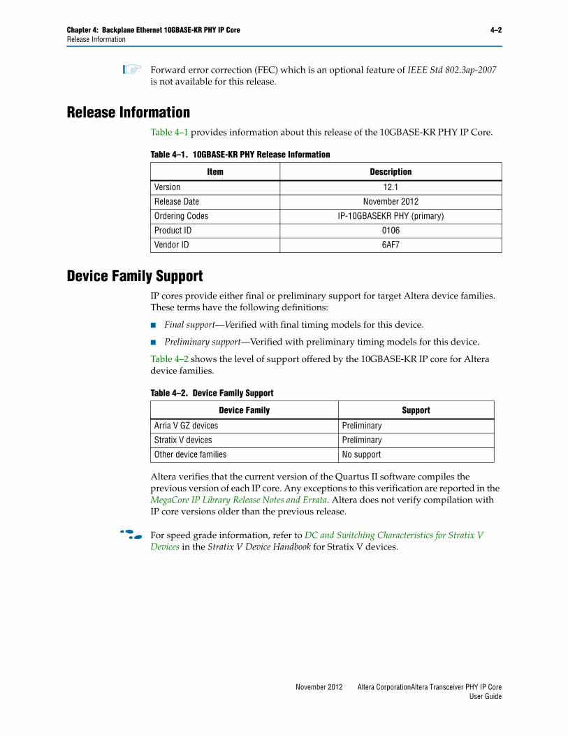
Chapter 4: Backplane Ethernet 10GBASE-KR PHY IP Core 4–2Release Information
1 Forward error correction (FEC) which is an optional feature of IEEE Std 802.3ap-2007 is not available for this release.
Release InformationTable 4–1 provides information about this release of the 10GBASE-KR PHY IP Core.
Device Family SupportIP cores provide either final or preliminary support for target Altera device families. These terms have the following definitions:
■ Final support—Verified with final timing models for this device.
■ Preliminary support—Verified with preliminary timing models for this device.
Table 4–2 shows the level of support offered by the 10GBASE-KR IP core for Altera device families.
Altera verifies that the current version of the Quartus II software compiles the previous version of each IP core. Any exceptions to this verification are reported in the MegaCore IP Library Release Notes and Errata. Altera does not verify compilation with IP core versions older than the previous release.
f For speed grade information, refer to DC and Switching Characteristics for Stratix V Devices in the Stratix V Device Handbook for Stratix V devices.
Table 4–1. 10GBASE-KR PHY Release Information
Item Description
Version 12.1
Release Date November 2012
Ordering Codes IP-10GBASEKR PHY (primary)
Product ID 0106
Vendor ID 6AF7
Table 4–2. Device Family Support
Device Family Support
Arria V GZ devices Preliminary
Stratix V devices Preliminary
Other device families No support
November 2012 Altera CorporationAltera Transceiver PHY IP CoreUser Guide
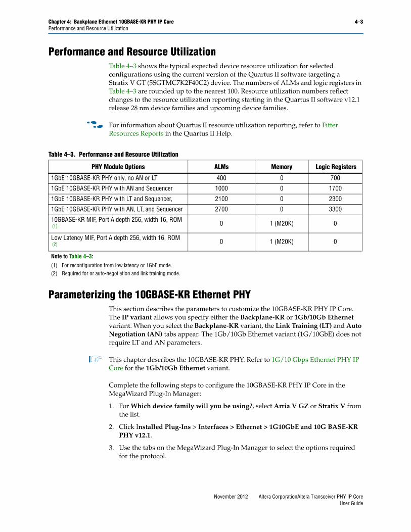
Chapter 4: Backplane Ethernet 10GBASE-KR PHY IP Core 4–3Performance and Resource Utilization
Performance and Resource Utilization Table 4–3 shows the typical expected device resource utilization for selected configurations using the current version of the Quartus II software targeting a Stratix V GT (5SGTMC7K2F40C2) device. The numbers of ALMs and logic registers in Table 4–3 are rounded up to the nearest 100. Resource utilization numbers reflect changes to the resource utilization reporting starting in the Quartus II software v12.1 release 28 nm device families and upcoming device families.
f For information about Quartus II resource utilization reporting, refer to Fitter Resources Reports in the Quartus II Help.
Parameterizing the 10GBASE-KR Ethernet PHYThis section describes the parameters to customize the 10GBASE-KR PHY IP Core. The IP variant allows you specify either the Backplane-KR or 1Gb/10Gb Ethernet variant. When you select the Backplane-KR variant, the Link Training (LT) and Auto Negotiation (AN) tabs appear. The 1Gb/10Gb Ethernet variant (1G/10GbE) does not require LT and AN parameters.
1 This chapter describes the 10GBASE-KR PHY. Refer to 1G/10 Gbps Ethernet PHY IP Core for the 1Gb/10Gb Ethernet variant.
Complete the following steps to configure the 10GBASE-KR PHY IP Core in the MegaWizard Plug-In Manager:
1. For Which device family will you be using?, select Arria V GZ or Stratix V from the list.
2. Click Installed Plug-Ins > Interfaces > Ethernet > 1G10GbE and 10G BASE-KR PHY v12.1.
3. Use the tabs on the MegaWizard Plug-In Manager to select the options required for the protocol.
Table 4–3. Performance and Resource Utilization
PHY Module Options ALMs Memory Logic Registers
1GbE 10GBASE-KR PHY only, no AN or LT 400 0 700
1GbE 10GBASE-KR PHY with AN and Sequencer 1000 0 1700
1GbE 10GBASE-KR PHY with LT and Sequencer, 2100 0 2300
1GbE 10GBASE-KR PHY with AN, LT, and Sequencer 2700 0 3300
10GBASE-KR MIF, Port A depth 256, width 16, ROM (1) 0 1 (M20K) 0
Low Latency MIF, Port A depth 256, width 16, ROM (2) 0 1 (M20K) 0
Note to Table 4–3:
(1) For reconfiguration from low latency or 1GbE mode.(2) Required for or auto-negotiation and link training mode.
November 2012 Altera CorporationAltera Transceiver PHY IP CoreUser Guide
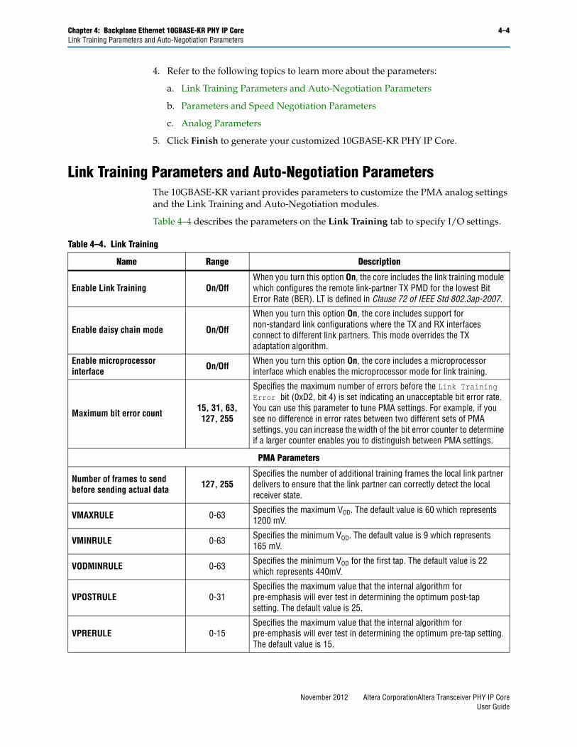
Chapter 4: Backplane Ethernet 10GBASE-KR PHY IP Core 4–4Link Training Parameters and Auto-Negotiation Parameters
4. Refer to the following topics to learn more about the parameters:
a. Link Training Parameters and Auto-Negotiation Parameters
b. Parameters and Speed Negotiation Parameters
c. Analog Parameters
5. Click Finish to generate your customized 10GBASE-KR PHY IP Core.
Link Training Parameters and Auto-Negotiation ParametersThe 10GBASE-KR variant provides parameters to customize the PMA analog settings and the Link Training and Auto-Negotiation modules.
Table 4–4 describes the parameters on the Link Training tab to specify I/O settings.
Table 4–4. Link Training
Name Range Description
Enable Link Training On/OffWhen you turn this option On, the core includes the link training module which configures the remote link-partner TX PMD for the lowest Bit Error Rate (BER). LT is defined in Clause 72 of IEEE Std 802.3ap-2007.
Enable daisy chain mode On/Off
When you turn this option On, the core includes support for non-standard link configurations where the TX and RX interfaces connect to different link partners. This mode overrides the TX adaptation algorithm.
Enable microprocessor interface On/Off When you turn this option On, the core includes a microprocessor
interface which enables the microprocessor mode for link training.
Maximum bit error count 15, 31, 63, 127, 255
Specifies the maximum number of errors before the Link Training Error bit (0xD2, bit 4) is set indicating an unacceptable bit error rate. You can use this parameter to tune PMA settings. For example, if you see no difference in error rates between two different sets of PMA settings, you can increase the width of the bit error counter to determine if a larger counter enables you to distinguish between PMA settings.
PMA Parameters
Number of frames to send before sending actual data 127, 255
Specifies the number of additional training frames the local link partner delivers to ensure that the link partner can correctly detect the local receiver state.
VMAXRULE 0-63 Specifies the maximum VOD. The default value is 60 which represents 1200 mV.
VMINRULE 0-63 Specifies the minimum VOD. The default value is 9 which represents 165 mV.
VODMINRULE 0-63 Specifies the minimum VOD for the first tap. The default value is 22 which represents 440mV.
VPOSTRULE 0-31Specifies the maximum value that the internal algorithm for pre-emphasis will ever test in determining the optimum post-tap setting. The default value is 25.
VPRERULE 0-15Specifies the maximum value that the internal algorithm for pre-emphasis will ever test in determining the optimum pre-tap setting. The default value is 15.
November 2012 Altera CorporationAltera Transceiver PHY IP CoreUser Guide
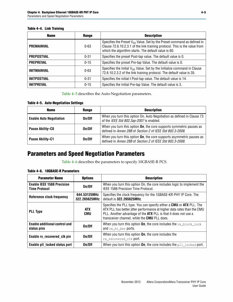
Chapter 4: Backplane Ethernet 10GBASE-KR PHY IP Core 4–5Parameters and Speed Negotiation Parameters
Table 4–5 describes the Auto-Negotiation parameters.
Parameters and Speed Negotiation ParametersTable 4–6 describes the parameters to specify 10GBASE-R PCS.
PREMAINVAL 0-63Specifies the Preset VOD Value. Set by the Preset command as defined in Clause 72.6.10.2.3.1 of the link training protocol. This is the value from which the algorithm starts. The default value is 60.
PREPOSTVAL 0-31 Specifies the preset Post-tap value. The default value is 0.
PREPREVAL 0-15 Specifies the preset Pre-tap Value. The default value is 0.
INITMAINVAL 0-63 Specifies the Initial VOD Value. Set by the Initialize command in Clause 72.6.10.2.3.2 of the link training protocol. The default value is 35.
INITPOSTVAL 0-31 Specifies the initial t Post-tap value. The default value is 14.
INITPREVAL 0-15 Specifies the Initial Pre-tap Value. The default value is 3.
Table 4–4. Link Training
Name Range Description
Table 4–5. Auto-Negotiation Settings
Name Range Description
Enable Auto Negotiation On/Off When you turn this option On, Auto Negotiation as defined in Clause 73 of the IEEE Std 802.3ap-2007 is enabled.
Pause Ability–C0 On/Off When you turn this option On, the core supports symmetric pauses as defined in Annex 28B of Section 2 of IEEE Std 802.3-2008.
Pause Ability–C1 On/Off When you turn this option On, the core supports asymmetric pauses as defined in Annex 28B of Section 2 of IEEE Std 802.3-2008.
Table 4–6. 10GBASE-R Parameters
Parameter Name Options Description
Enable IEEE 1588 Precision Time Protocol On/Off When you turn this option On, the core includes logic to implement the
IEEE 1588 Precision Time Protocol.
Reference clock frequency 644.53125MHz 322.265625MHz
Specifies the clock frequency for the 1GBASE-KR PHY IP Core. The default is 322.265625MHz.
PLL Type ATXCMU
Specifies the PLL type. You can specify either a CMU or ATX PLL. The ATX PLL has better jitter performance at higher data rates than the CMU PLL. Another advantage of the ATX PLL is that it does not use a transceiver channel, while the CMU PLL does.
Enable additional control and status pins On/Off When you turn this option On, the core includes the rx_block_lock
and rx_hi_ber ports.
Enable rx_recovered_clk pin On/Off When you turn this option On, the core includes the rx_recovered_clk port.
Enable pll_locked status port On/Off When you turn this option On, the core includes the pll_locked port.
November 2012 Altera CorporationAltera Transceiver PHY IP CoreUser Guide
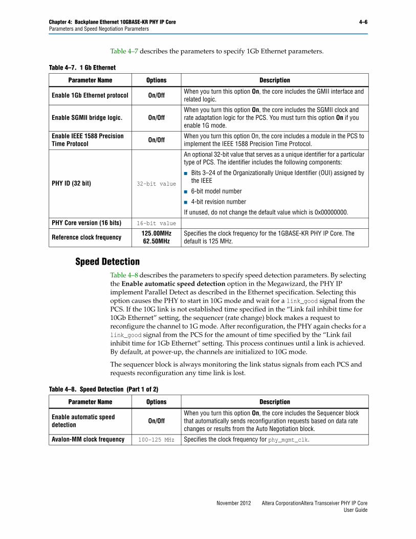
Chapter 4: Backplane Ethernet 10GBASE-KR PHY IP Core 4–6Parameters and Speed Negotiation Parameters
Table 4–7 describes the parameters to specify 1Gb Ethernet parameters.
Speed DetectionTable 4–8 describes the parameters to specify speed detection parameters. By selecting the Enable automatic speed detection option in the Megawizard, the PHY IP implement Parallel Detect as described in the Ethernet specification. Selecting this option causes the PHY to start in 10G mode and wait for a link_good signal from the PCS. If the 10G link is not established time specified in the “Link fail inhibit time for 10Gb Ethernet” setting, the sequencer (rate change) block makes a request to reconfigure the channel to 1G mode. After reconfiguration, the PHY again checks for a link_good signal from the PCS for the amount of time specified by the “Link fail inhibit time for 1Gb Ethernet” setting. This process continues until a link is achieved. By default, at power-up, the channels are initialized to 10G mode.
The sequencer block is always monitoring the link status signals from each PCS and requests reconfiguration any time link is lost..
Table 4–7. 1 Gb Ethernet
Parameter Name Options Description
Enable 1Gb Ethernet protocol On/Off When you turn this option On, the core includes the GMII interface and related logic.
Enable SGMII bridge logic. On/OffWhen you turn this option On, the core includes the SGMII clock and rate adaptation logic for the PCS. You must turn this option On if you enable 1G mode.
Enable IEEE 1588 Precision Time Protocol On/Off When you turn this option On, the core includes a module in the PCS to
implement the IEEE 1588 Precision Time Protocol.
PHY ID (32 bit) 32-bit value
An optional 32-bit value that serves as a unique identifier for a particular type of PCS. The identifier includes the following components:
■ Bits 3–24 of the Organizationally Unique Identifier (OUI) assigned by the IEEE
■ 6-bit model number
■ 4-bit revision number
If unused, do not change the default value which is 0x00000000.
PHY Core version (16 bits) 16-bit value
Reference clock frequency 125.00MHz 62.50MHz
Specifies the clock frequency for the 1GBASE-KR PHY IP Core. The default is 125 MHz.
Table 4–8. Speed Detection (Part 1 of 2)
Parameter Name Options Description
Enable automatic speed detection On/Off
When you turn this option On, the core includes the Sequencer block that automatically sends reconfiguration requests based on data rate changes or results from the Auto Negotiation block.
Avalon-MM clock frequency 100–125 MHz Specifies the clock frequency for phy_mgmt_clk.
November 2012 Altera CorporationAltera Transceiver PHY IP CoreUser Guide
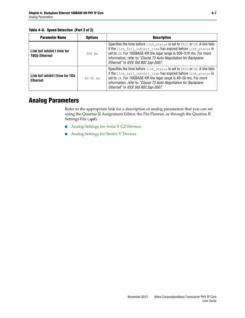
Chapter 4: Backplane Ethernet 10GBASE-KR PHY IP Core 4–7Analog Parameters
Analog ParametersRefer to the appropriate link for a description of analog parameters that you can set using the Quartus II Assignment Editor, the Pin Planner, or through the Quartus II Settings File (.qsf).
■ Analog Settings for Arria V GZ Devices
■ Analog Settings for Stratix V Devices
Link fail inhibit t time for 10Gb Ethernet 504 ms
Specifies the time before link_status is set to FAIL or OK. A link fails if the link_fail_inhibit_time has expired before link_status is set to OK. For 10GBASE-KR the legal range is 500–510 ms. For more information, refer to “Clause 73 Auto-Negotiation for Backplane Ethernet” in IEEE Std 802.3ap-2007.
Link fail inhibit t time for 1Gb Ethernet 40–50 ms
Specifies the time before link_status is set to FAIL or OK. A link fails if the link_fail_inhibit_time has expired before link_status is set to OK. For 10GBASE-KR the legal range is 40–50 ms. For more information, refer to “Clause 73 Auto-Negotiation for Backplane Ethernet” in IEEE Std 802.3ap-2007.
Table 4–8. Speed Detection (Part 2 of 2)
Parameter Name Options Description
November 2012 Altera CorporationAltera Transceiver PHY IP CoreUser Guide
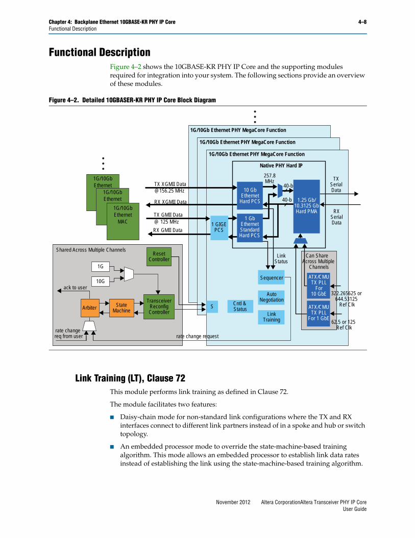
Chapter 4: Backplane Ethernet 10GBASE-KR PHY IP Core 4–8Functional Description
Functional Description Figure 4–2 shows the 10GBASE-KR PHY IP Core and the supporting modules required for integration into your system. The following sections provide an overview of these modules.
Link Training (LT), Clause 72This module performs link training as defined in Clause 72.
The module facilitates two features:
■ Daisy-chain mode for non-standard link configurations where the TX and RX interfaces connect to different link partners instead of in a spoke and hub or switch topology.
■ An embedded processor mode to override the state-machine-based training algorithm. This mode allows an embedded processor to establish link data rates instead of establishing the link using the state-machine-based training algorithm.
Figure 4–2. Detailed 10GBASER-KR PHY IP Core Block Diagram
1G/10GbEthernet
MAC
1G/10Gb Ethernet PHY MegaCore Function
1G/10Gb Ethernet PHY MegaCore Function
1G/10Gb Ethernet PHY MegaCore Function
Native PHY Hard IP
257.8MHz
40-b
40-bTX
SerialData
RXSerialData
1.25 Gb/10.3125 GbHard PMA
LinkStatus
Sequencer
S
ResetController
StateMachineArbiter
rate change request
ack to user
rate change req from user
TransceiverReconfigController
AutoNegotiation
LinkTraining
10 GbEthernet
Hard PCS
Cntl & Status
RX GMII Data
TX GMII Data@ 125 MHz
RX XGMII Data
TX XGMII Data
Shared Across Multiple Channels
@156.25 MHz
1 GIGEPCS
1G/10GbEthernet
MAC1G/10GbEthernet
MAC
1G
10G
1 GbEthernetStandardHard PCS
322.265625 or 644.53125
Ref Clk
62.5 or 125 Ref Clk
ATX/CMUTX PLL
For10 GbE
ATX/CMUTX PLL
For 1 GbE
Can Share Across Multiple
Channels
November 2012 Altera CorporationAltera Transceiver PHY IP CoreUser Guide

Chapter 4: Backplane Ethernet 10GBASE-KR PHY IP Core 4–9Functional Description
Auto Negotiation (AN), Clause 73The Auto Negotiation module in the 10GBASE-KR PHY IP implements Clause 73 of the Ethernet standard. This module currently supports auto negotiation between 1GbE and 10GBASE-R data rates. Auto negotiation with XAUI is not supported.
Auto negotiation is run upon power up or if the auto negotiation module is reset.
November 2012 Altera CorporationAltera Transceiver PHY IP CoreUser Guide

Chapter 4: Backplane Ethernet 10GBASE-KR PHY IP Core 4–10Interfaces
InterfacesFigure 4–3 shows the top-level signals of the Backplane Ethernet 10GBASE-KR IP Core.
Figure 4–3. 10GBASE-KR Top-Level Signals
xgmii_tx_dc[71:0]xgmii_tx_clkxgmii_rx_dc[71:0]xgmii_rx_clkgmii_tx_d[7:0]gmii_rx_d[7:0]gmii_tx_engmii_tx_errgmii_rx_errgmii_rx_dvled_char_errled_linkled_disp_errled_an
mgmt_clkmgmt_clk_resetmgmt_address[7:0]mgmt_writedata[31:0]mgmt_readdata[31:0]mgmt_writemgmt_readmgmt_waitrequest
rx_recovered_clktx_clkout_1grx_clkout_1grx_coreclkin_1gtx_coreclkin_1gpll_ref_clk_1gpll_ref_clk_10gpll_powerdown_1gpll_powerdown_10gtx_analogresettx_digitalresetrx_analogresetrx_digitalresetusr_an_lt_resetusr_seq_reset
upi_mode_enupi_adj[1:0]upe_incupi_decupi_preupi_initupi_st_bertupi_train_errupi_lock_errupi_rx_trainedupo_enableupo_frame_lockupo_cm_doneupo_bert_doneupo_ber_cnt[<w>-1:0]upo_ber_maxupo_coef_max
10GBASE-KR Top-Level Signals
DynamicReconfiguration
rx_serial_datatx_serial_data
reconfig_to_xcvr[(<n>70-1):0]reconfig_from_xcvr[(<n>46-1):0]
rc_busylt_start_rc
main_rc[5:0]post_rc[4:0]pre_rc[3:0]
tap_to_update[2:0]seq_start_rc
pcs_mode_rc[5:0]mode_1g_10gbar
en_lcl_rxeqrxeq_done
rx_block_lockrx_hi_berpll_locked
rx_is_lockedtodatatx_cal_busyrx_cal_busycalc_clk_1g
rx_data_readyrx_sync_status
tx_pcfifo_error_1grx_pcfifo_errog_1g
lcl_rftm_in_trigger[3:0]
tm_out_trigger[3:0]rx_rlv
rx_clksliprx_latency_adj_1g[11:0]tx_latency_adj_1g[11:0]
rx_latency_adj_10g[11:0]tx_latency_adj_10g[11:0]
dmi_mode_endmi_frame_lock
dmi_rmt_rx_readydmi_lcl_coefl[5:0]
dmi_lcl_coefh[1:0]dmi_lcl_upd_new
dmi_rx_traineddmo_frame_lock
dmo_rmt_rx_readydmo_lcl_coefl[5:0]
dmo_lcl_coefh[1:0]dmo_lcl_upd_new
dmo_rx_trained
TransceiverSerial Data
XGMII and GMII Interfaces
Avalon-MM PHYManagement
Interface
Daisy ChainMode InputInterface
(10GBASE-KROnly)
Embedded ProcessorInterface
(10GBASE-KROnly)
Clocks andReset
Interface
Status
November 2012 Altera CorporationAltera Transceiver PHY IP CoreUser Guide
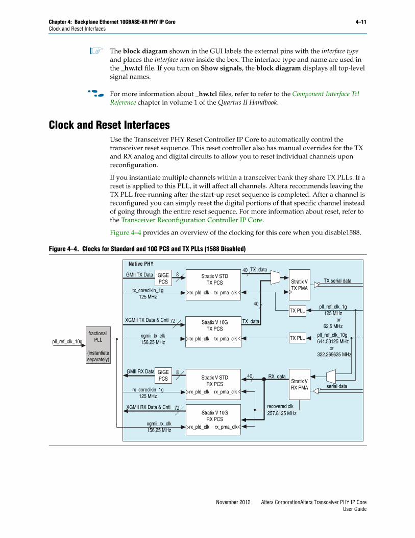
Chapter 4: Backplane Ethernet 10GBASE-KR PHY IP Core 4–11Clock and Reset Interfaces
1 The block diagram shown in the GUI labels the external pins with the interface type and places the interface name inside the box. The interface type and name are used in the _hw.tcl file. If you turn on Show signals, the block diagram displays all top-level signal names.
f For more information about _hw.tcl files, refer to refer to the Component Interface Tcl Reference chapter in volume 1 of the Quartus II Handbook.
Clock and Reset InterfacesUse the Transceiver PHY Reset Controller IP Core to automatically control the transceiver reset sequence. This reset controller also has manual overrides for the TX and RX analog and digital circuits to allow you to reset individual channels upon reconfiguration.
If you instantiate multiple channels within a transceiver bank they share TX PLLs. If a reset is applied to this PLL, it will affect all channels. Altera recommends leaving the TX PLL free-running after the start-up reset sequence is completed. After a channel is reconfigured you can simply reset the digital portions of that specific channel instead of going through the entire reset sequence. For more information about reset, refer to the Transceiver Reconfiguration Controller IP Core.
Figure 4–4 provides an overview of the clocking for this core when you disable1588.
Figure 4–4. Clocks for Standard and 10G PCS and TX PLLs (1588 Disabled)
xgmii_rx_clk156.25 MHz
xgmii_tx_clk156.25 MHz
Native PHY
Stratix V STDRX PCS
Stratix VTX PMAtx_coreclkin_1g
125 MHz
Stratix VRX PMA
TX PLL
TX PLL
40
rx_pld_clk rx_pma_clk
TX serial data8GMII TX Data
72XGMII TX Data & Cntl
RX data
40 TX data
40
TX data
serial data
pll_ref_clk_10g644.53125 MHz or 322.265625 MHz
pll_ref_clk_1g125 MHz or 62.5 MHz
Stratix V STDTX PCS
tx_pld_clk tx_pma_clk
8GMII RX Data
pll_ref_clk_10g
72XGMII RX Data & Cntl recovered clk257.8125 MHz
rx_coreclkin_1g125 MHz
Stratix V 10GRX PCS
rx_pld_clk rx_pma_clk
Stratix V 10GTX PCS
tx_pld_clk tx_pma_clkfractional
PLL
(instantiateseparately)
GIGEPCS
GIGEPCS
November 2012 Altera CorporationAltera Transceiver PHY IP CoreUser Guide
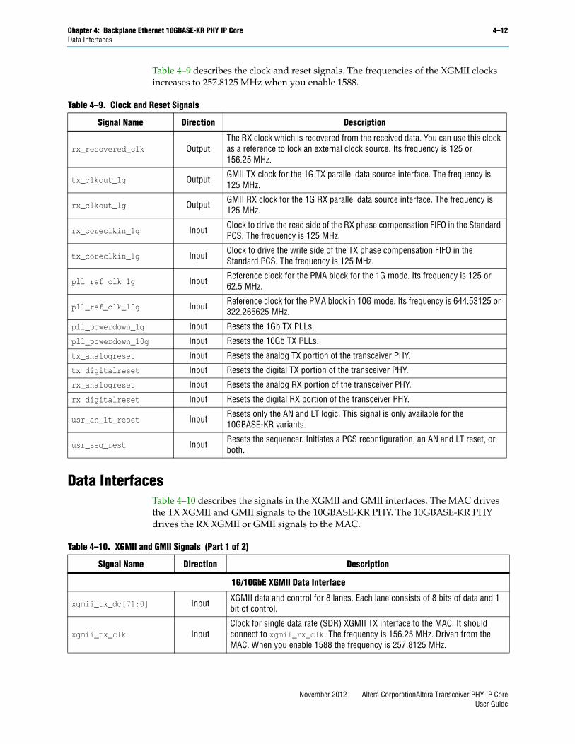
Chapter 4: Backplane Ethernet 10GBASE-KR PHY IP Core 4–12Data Interfaces
Table 4–9 describes the clock and reset signals. The frequencies of the XGMII clocks increases to 257.8125 MHz when you enable 1588.
Data Interfaces Table 4–10 describes the signals in the XGMII and GMII interfaces. The MAC drives the TX XGMII and GMII signals to the 10GBASE-KR PHY. The 10GBASE-KR PHY drives the RX XGMII or GMII signals to the MAC.
Table 4–9. Clock and Reset Signals
Signal Name Direction Description
rx_recovered_clk OutputThe RX clock which is recovered from the received data. You can use this clock as a reference to lock an external clock source. Its frequency is 125 or 156.25 MHz.
tx_clkout_1g Output GMII TX clock for the 1G TX parallel data source interface. The frequency is 125 MHz.
rx_clkout_1g Output GMII RX clock for the 1G RX parallel data source interface. The frequency is 125 MHz.
rx_coreclkin_1g Input Clock to drive the read side of the RX phase compensation FIFO in the Standard PCS. The frequency is 125 MHz.
tx_coreclkin_1g Input Clock to drive the write side of the TX phase compensation FIFO in the Standard PCS. The frequency is 125 MHz.
pll_ref_clk_1g Input Reference clock for the PMA block for the 1G mode. Its frequency is 125 or 62.5 MHz.
pll_ref_clk_10g Input Reference clock for the PMA block in 10G mode. Its frequency is 644.53125 or 322.265625 MHz.
pll_powerdown_1g Input Resets the 1Gb TX PLLs.
pll_powerdown_10g Input Resets the 10Gb TX PLLs.
tx_analogreset Input Resets the analog TX portion of the transceiver PHY.
tx_digitalreset Input Resets the digital TX portion of the transceiver PHY.
rx_analogreset Input Resets the analog RX portion of the transceiver PHY.
rx_digitalreset Input Resets the digital RX portion of the transceiver PHY.
usr_an_lt_reset Input Resets only the AN and LT logic. This signal is only available for the 10GBASE-KR variants.
usr_seq_rest Input Resets the sequencer. Initiates a PCS reconfiguration, an AN and LT reset, or both.
Table 4–10. XGMII and GMII Signals (Part 1 of 2)
Signal Name Direction Description
1G/10GbE XGMII Data Interface
xgmii_tx_dc[71:0] Input XGMII data and control for 8 lanes. Each lane consists of 8 bits of data and 1 bit of control.
xgmii_tx_clk Input Clock for single data rate (SDR) XGMII TX interface to the MAC. It should connect to xgmii_rx_clk. The frequency is 156.25 MHz. Driven from the MAC. When you enable 1588 the frequency is 257.8125 MHz.
November 2012 Altera CorporationAltera Transceiver PHY IP CoreUser Guide
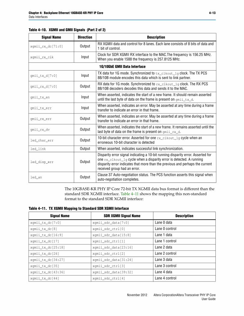
Chapter 4: Backplane Ethernet 10GBASE-KR PHY IP Core 4–13Data Interfaces
The 10GBASE-KR PHY IP Core 72-bit TX XGMII data bus format is different than the standard SDR XGMII interface. Table 4–11 shows the mapping this non-standard format to the standard SDR XGMII interface:
xgmii_rx_dc[71:0] Output RX XGMII data and control for 8 lanes. Each lane consists of 8 bits of data and 1 bit of control.
xgmii_rx_clk Input Clock for SDR XGMII RX interface to the MAC.The frequency is 156.25 MHz. When you enable 1588 the frequency is 257.8125 MHz.
1G/10GbE GMII Data Interface
gmii_tx_d[7:0] Input TX data for 1G mode. Synchronized to tx_clkout_1g clock. The TX PCS 8B/10B module encodes this data which is sent to link partner.
gmii_rx_d[7:0] Output RX data for 1G mode. Synchronized to rx_clkout_1g clock. The RX PCS 8B/10B decoders decodes this data and sends it to the MAC.
gmii_tx_en Input When asserted, indicates the start of a new frame. It should remain asserted until the last byte of data on the frame is present on gmii_tx_d.
gmii_tx_err Input When asserted, indicates an error. May be asserted at any time during a frame transfer to indicate an error in that frame.
gmii_rx_err Output When asserted, indicates an error. May be asserted at any time during a frame transfer to indicate an error in that frame.
gmii_rx_dv Output When asserted, indicates the start of a new frame. It remains asserted until the last byte of data on the frame is present on gmii_rx_d.
led_char_err Output 10-bit character error. Asserted for one rx_clkout_1g cycle when an erroneous 10-bit character is detected
led_link Output When asserted, indicates successful link synchronization.
led_disp_err Output
Disparity error signal indicating a 10-bit running disparity error. Asserted for one rx_clkout_1g cycle when a disparity error is detected. A running disparity error indicates that more than the previous and perhaps the current received group had an error.
led_an Output Clause 37 Auto-negotiation status. The PCS function asserts this signal when auto-negotiation completes.
Table 4–10. XGMII and GMII Signals (Part 2 of 2)
Signal Name Direction Description
Table 4–11. TX XGMII Mapping to Standard SDR XGMII Interface
Signal Name SDR XGMII Signal Name Description
xgmii_tx_dc[7:0] xgmii_sdr_data[7:0] Lane 0 data
xgmii_tx_dc[8] xgmii_sdr_ctrl[0] Lane 0 control
xgmii_tx_dc[16:9] xgmii_sdr_data[15:8] Lane 1 data
xgmii_tx_dc[17] xgmii_sdr_ctrl[1] Lane 1 control
xgmii_tx_dc[25:18] xgmii_sdr_data[23:16] Lane 2 data
xgmii_tx_dc[26] xgmii_sdr_ctrl[2] Lane 2 control
xgmii_tx_dc[34:27] xgmii_sdr_data[31:24] Lane 3 data
xgmii_tx_dc[35] xgmii_sdr_ctrl[3] Lane 3 control
xgmii_tx_dc[43:36] xgmii_sdr_data[39:32] Lane 4 data
xgmii_tx_dc[44] xgmii_sdr_ctrl[4] Lane 4 control
November 2012 Altera CorporationAltera Transceiver PHY IP CoreUser Guide
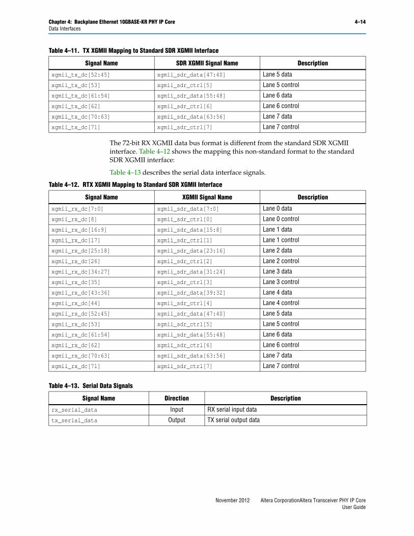
Chapter 4: Backplane Ethernet 10GBASE-KR PHY IP Core 4–14Data Interfaces
The 72-bit RX XGMII data bus format is different from the standard SDR XGMII interface. Table 4–12 shows the mapping this non-standard format to the standard SDR XGMII interface:
Table 4–13 describes the serial data interface signals.
xgmii_tx_dc[52:45] xgmii_sdr_data[47:40] Lane 5 data
xgmii_tx_dc[53] xgmii_sdr_ctrl[5] Lane 5 control
xgmii_tx_dc[61:54] xgmii_sdr_data[55:48] Lane 6 data
xgmii_tx_dc[62] xgmii_sdr_ctrl[6] Lane 6 control
xgmii_tx_dc[70:63] xgmii_sdr_data[63:56] Lane 7 data
xgmii_tx_dc[71] xgmii_sdr_ctrl[7] Lane 7 control
Table 4–11. TX XGMII Mapping to Standard SDR XGMII Interface
Signal Name SDR XGMII Signal Name Description
Table 4–12. RTX XGMII Mapping to Standard SDR XGMII Interface
Signal Name XGMII Signal Name Description
xgmii_rx_dc[7:0] xgmii_sdr_data[7:0] Lane 0 data
xgmii_rx_dc[8] xgmii_sdr_ctrl[0] Lane 0 control
xgmii_rx_dc[16:9] xgmii_sdr_data[15:8] Lane 1 data
xgmii_rx_dc[17] xgmii_sdr_ctrl[1] Lane 1 control
xgmii_rx_dc[25:18] xgmii_sdr_data[23:16] Lane 2 data
xgmii_rx_dc[26] xgmii_sdr_ctrl[2] Lane 2 control
xgmii_rx_dc[34:27] xgmii_sdr_data[31:24] Lane 3 data
xgmii_rx_dc[35] xgmii_sdr_ctrl[3] Lane 3 control
xgmii_rx_dc[43:36] xgmii_sdr_data[39:32] Lane 4 data
xgmii_rx_dc[44] xgmii_sdr_ctrl[4] Lane 4 control
xgmii_rx_dc[52:45] xgmii_sdr_data[47:40] Lane 5 data
xgmii_rx_dc[53] xgmii_sdr_ctrl[5] Lane 5 control
xgmii_rx_dc[61:54] xgmii_sdr_data[55:48] Lane 6 data
xgmii_rx_dc[62] xgmii_sdr_ctrl[6] Lane 6 control
xgmii_rx_dc[70:63] xgmii_sdr_data[63:56] Lane 7 data
xgmii_rx_dc[71] xgmii_sdr_ctrl[7] Lane 7 control
Table 4–13. Serial Data Signals
Signal Name Direction Description
rx_serial_data Input RX serial input data
tx_serial_data Output TX serial output data
November 2012 Altera CorporationAltera Transceiver PHY IP CoreUser Guide
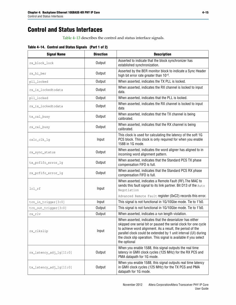
Chapter 4: Backplane Ethernet 10GBASE-KR PHY IP Core 4–15Control and Status Interfaces
Control and Status InterfacesTable 4–13 describes the control and status interface signals.
Table 4–14. Control and Status Signals (Part 1 of 2)
Signal Name Direction Description
rx_block_lock Output Asserted to indicate that the block synchronizer has established synchronization.
rx_hi_ber Output Asserted by the BER monitor block to indicate a Sync Header high bit error rate greater than 10-4.
pll_locked Output When asserted, indicates the TX PLL is locked.
rx_is_lockedtodata Output When asserted, indicates the RX channel is locked to input data.
pll_locked Output When asserted, indicates that the PLL is locked.
rx_is_lockedtodata Output When asserted, indicates the RX channel is locked to input data
tx_cal_busy Output When asserted, indicates that the TX channel is being calibrated.
rx_cal_busy Output When asserted, indicates that the RX channel is being calibrated.
calc_clk_1g InputThis clock is used for calculating the latency of the soft 1G PCS block. This clock is only required for when you enable 1588 in 1G mode.
rx_sync_status Output When asserted, indicates the word aligner has aligned to in incoming word alignment pattern.
tx_pcfifo_error_1g Output When asserted, indicates that the Standard PCS TX phase compensation FIFO is full.
rx_pcfifo_error_1g Output When asserted, indicates that the Standard PCS RX phase compensation FIFO is full.
lcl_rf Input
When asserted, indicates a Remote Fault (RF).The MAC to sends this fault signal to its link partner. Bit D13 of the Auto Negotiation
Advanced Remote Fault register (0xC2) records this error.
trn_in_trigger[3:0] Input This signal is not functional in 1G/10Gbe mode. Tie to 1’b0.
trn_out_trigger[3:0] Output This signal is not functional in 1G/10Gbe mode. Tie to 1’b0.
rx_rlv Output When asserted, indicates a run length violation.
rx_clkslip Input
When asserted, indicates that the deserializer has either skipped one serial bit or paused the serial clock for one cycle to achieve word alignment. As a result, the period of the parallel clock could be extended by 1 unit interval (UI) during the clock slip operation. This signal is available if you select the optional
rx_latency_adj_1g[11:0] OutputWhen you enable 1588, this signal outputs the real time latency in GMII clock cycles (125 MHz) for the RX PCS and PMA datapath for 1G mode.
tx_latency_adj_1g[11:0] OutputWhen you enable 1588, this signal outputs real time latency in GMII clock cycles (125 MHz) for the TX PCS and PMA datapath for 1G mode.
November 2012 Altera CorporationAltera Transceiver PHY IP CoreUser Guide
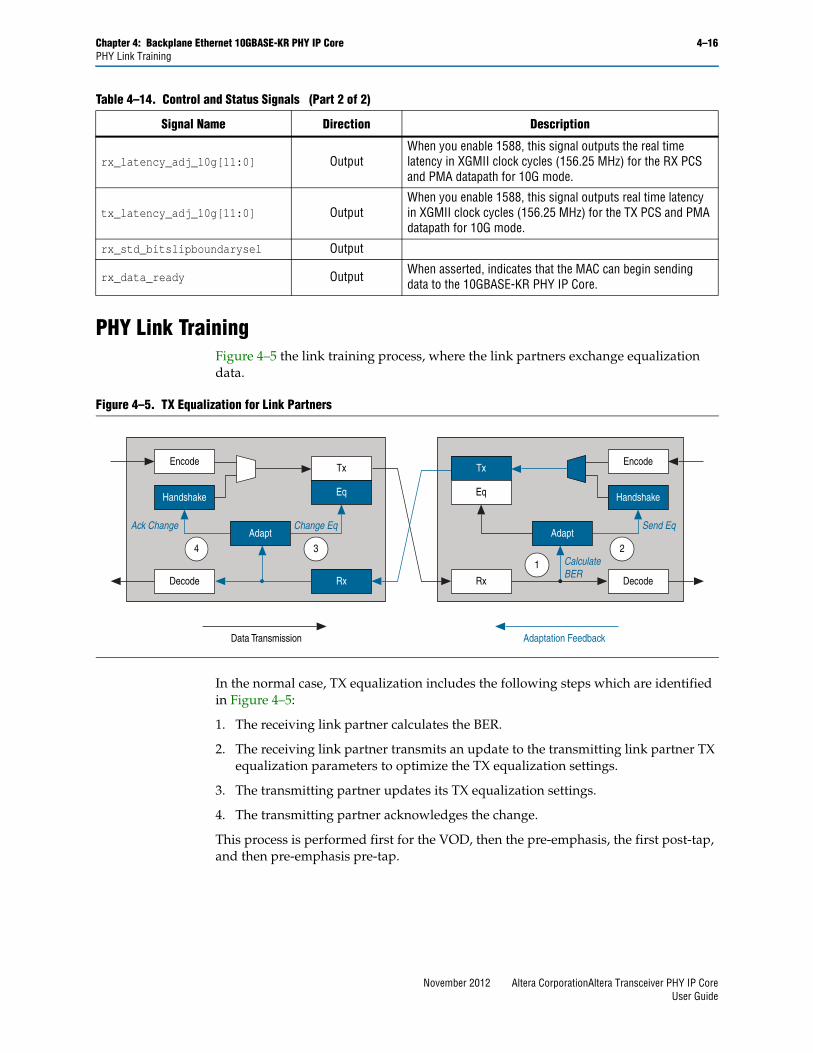
Chapter 4: Backplane Ethernet 10GBASE-KR PHY IP Core 4–16PHY Link Training
PHY Link TrainingFigure 4–5 the link training process, where the link partners exchange equalization data.
In the normal case, TX equalization includes the following steps which are identified in Figure 4–5:
1. The receiving link partner calculates the BER.
2. The receiving link partner transmits an update to the transmitting link partner TX equalization parameters to optimize the TX equalization settings.
3. The transmitting partner updates its TX equalization settings.
4. The transmitting partner acknowledges the change.
This process is performed first for the VOD, then the pre-emphasis, the first post-tap, and then pre-emphasis pre-tap.
rx_latency_adj_10g[11:0] OutputWhen you enable 1588, this signal outputs the real time latency in XGMII clock cycles (156.25 MHz) for the RX PCS and PMA datapath for 10G mode.
tx_latency_adj_10g[11:0] OutputWhen you enable 1588, this signal outputs real time latency in XGMII clock cycles (156.25 MHz) for the TX PCS and PMA datapath for 10G mode.
rx_std_bitslipboundarysel Output
rx_data_ready Output When asserted, indicates that the MAC can begin sending data to the 10GBASE-KR PHY IP Core.
Table 4–14. Control and Status Signals (Part 2 of 2)
Signal Name Direction Description
Figure 4–5. TX Equalization for Link Partners
Rx
Encode
Handshake
Adapt
Tx
Eq
Decode Rx
Encode
Handshake
Adapt
Tx
Eq
Decode
CalculateBER
Send EqChange EqAck Change
Data Transmission Adaptation Feedback
1
234
November 2012 Altera CorporationAltera Transceiver PHY IP CoreUser Guide
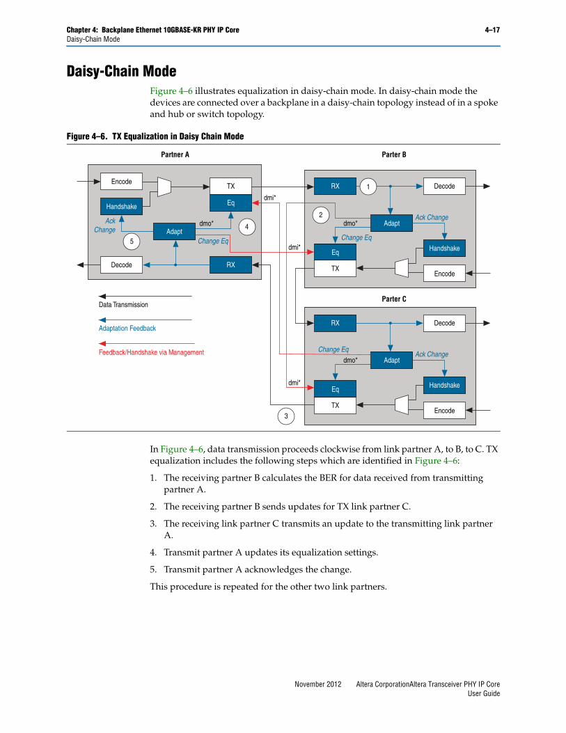
Chapter 4: Backplane Ethernet 10GBASE-KR PHY IP Core 4–17Daisy-Chain Mode
Daisy-Chain Mode Figure 4–6 illustrates equalization in daisy-chain mode. In daisy-chain mode the devices are connected over a backplane in a daisy-chain topology instead of in a spoke and hub or switch topology.
In Figure 4–6, data transmission proceeds clockwise from link partner A, to B, to C. TX equalization includes the following steps which are identified in Figure 4–6:
1. The receiving partner B calculates the BER for data received from transmitting partner A.
2. The receiving partner B sends updates for TX link partner C.
3. The receiving link partner C transmits an update to the transmitting link partner A.
4. Transmit partner A updates its equalization settings.
5. Transmit partner A acknowledges the change.
This procedure is repeated for the other two link partners.
Figure 4–6. TX Equalization in Daisy Chain Mode
RX
Encode
Handshake
Adapt
TX
dmi*
dmi*
dmi*
dmo*dmo*
Partner A
Parter C
Parter B
Eq
Decode
RX
Encode
Handshake
Adapt
TX
Eq
Decode
Change Eq
AckChange
Data Transmission
Adaptation Feedback
Change Eq
Ack Change
Feedback/Handshake via Management
RX
Encode
Handshake
Adapt
TX
Eq
Decode
Change EqAck Change
1
2
3
4
5
dmo*
November 2012 Altera CorporationAltera Transceiver PHY IP CoreUser Guide
Chapter 4: Backplane Ethernet 10GBASE-KR PHY IP Core 4–18Embedded Processor Mode Interface
Table 4–15 describes the signals that permit a daisy-chain mode for Link Training.
Embedded Processor Mode InterfaceTable 4–16 describes the signals that allow you to use the embedded processor mode of Link Training. This mode overrides the TX adaptation algorithm and allows an embedded processor to initialize the link.
Table 4–15. Daisy Chain Mode
Signal Name Role Description
dmi_mode_en input When asserted, enable Daisy Chain mode.
dmi_frame_lock input When asserted, the daisy chain state machine has locked to the training frames.
dmi_rmt_rx_ready Input Corresponds to bit 15 of Status report field. When asserted, the remote receiver.
dmi_lcl_coefl[5:0] InputLocal update low bits[5:0]. In daisy-chained configurations, the local update coefficients substitute for the coefficients that would be set using Link Training.
dmi_lcl_coefh[1:0] InputLocal update high bits[13:12]. In daisy-chained configurations, the local update coefficients substitute for the coefficients that would be set using Link Training.
dmi_lcl_upd_new Input When asserted, indicates a local update has occurred.
dmi_rx_trained input When asserted, indicates that the state machine has finished local training.
dmo_frame_lock Output When asserted, indicates that the state machine has locked to the training frames.
dmo_rmt_rx_ready Output Corresponds to the link partner’s remote receiver ready bit.
dmo_lcl_coefl[5:0] OutputLocal update low bits[5:0]. In daisy-chained configurations, the local update coefficients substitute for the coefficients that would be set using Link Training.
dmo_lcl_coefh[1:0] OutputLocal update high bits[13:12]. In daisy-chained configurations, the local update coefficients substitute for the coefficients that would be set using Link Training.
dmo_lcl_upd_new Output When asserted, indicates a local update has occurred.
dmo_rx_trained Output When asserted, indicates that the state machine has finished local training.
Table 4–16. Embedded Processor Link Training Signals (Part 1 of 2)
Signal Name Role Description
upi_mode_en Input When asserted, enables embedded processor mode.
upi_adj[1:0]
Input
Selects the active tap. The following encodings are defined:
■ 2’b01: Main tap
■ 2’b10: Post-tap
■ 2’b11 Pre-tap
upi_inc Input When asserted, sends the increment command.
upi_dec Input When asserted, sends the decrement command.
November 2012 Altera CorporationAltera Transceiver PHY IP CoreUser Guide
Chapter 4: Backplane Ethernet 10GBASE-KR PHY IP Core 4–19Register Interface and Register Descriptions
Register Interface and Register DescriptionsTable 4–17 describes the signals that comprise the Avalon-MM PHY Management interface.
f Refer to the “Typical Slave Read and Write Transfers” and “Master Transfers” sections in the “Avalon Memory-Mapped Interfaces” chapter of the Avalon Interface Specifications for timing diagrams.
upi_pre Input When asserted, sends the preset command.
upi_init Input When asserted, sends the initialize command.
upi_st_bert Input When asserted, starts the BER timer.
upi_train_err Input When asserted, indicates a training error.
upi_rx_trained Input When asserted, the local RX interface is trained
upo_enable Output When asserted, indicates that the 10GBASE-KR PHY IP Core is ready to receive commands from the embedded processor.
upo_frame_lock Output When asserted, indicates the receiver has achieved training frame lock.
upo_cm_done Output When asserted, indicates the master state machine handshake is complete.
upo_bert_done Output When asserted, indicates the BER timer is at its maximum count.
upo_ber_cnt[<w>-1:0] Output Records the BER count.
upo_ber_max Output When asserted, the BER counter has rolled over.
upo_coef_max Output When asserted, indicates that the remote coefficients are at their maximum or minimum values.
Table 4–16. Embedded Processor Link Training Signals (Part 2 of 2)
Signal Name Role Description
Table 4–17. Avalon-MM PHY Management Signals
Signal Name Direction Description
mgmt_clk Input
The clock signal that controls the Avalon-MM PHY management, interface. If you plan to use the same clock for the PHY management interface and transceiver reconfiguration, you must restrict the frequency range of mgmt_clk to 100–125 MHz to meet the specification for the transceiver reconfiguration clock.
mgmt_clk_reset Input Resets the PHY management interface. This signal is active high and level sensitive.
mgmt_addr[7:0] Input 8-bit Avalon-MM address.
mgmt_writedata[31:0] Input Input data.
mgmt_readdata[31:0] Output Output data.
mgmt_write Input Write signal. Active high.
mgmt_read Input Read signal. Active high.
mgmt_waitrequest OutputWhen asserted, indicates that the Avalon-MM slave interface is unable to respond to a read or write request. When asserted, control signals to the Avalon-MM slave interface must remain constant.
November 2012 Altera CorporationAltera Transceiver PHY IP CoreUser Guide
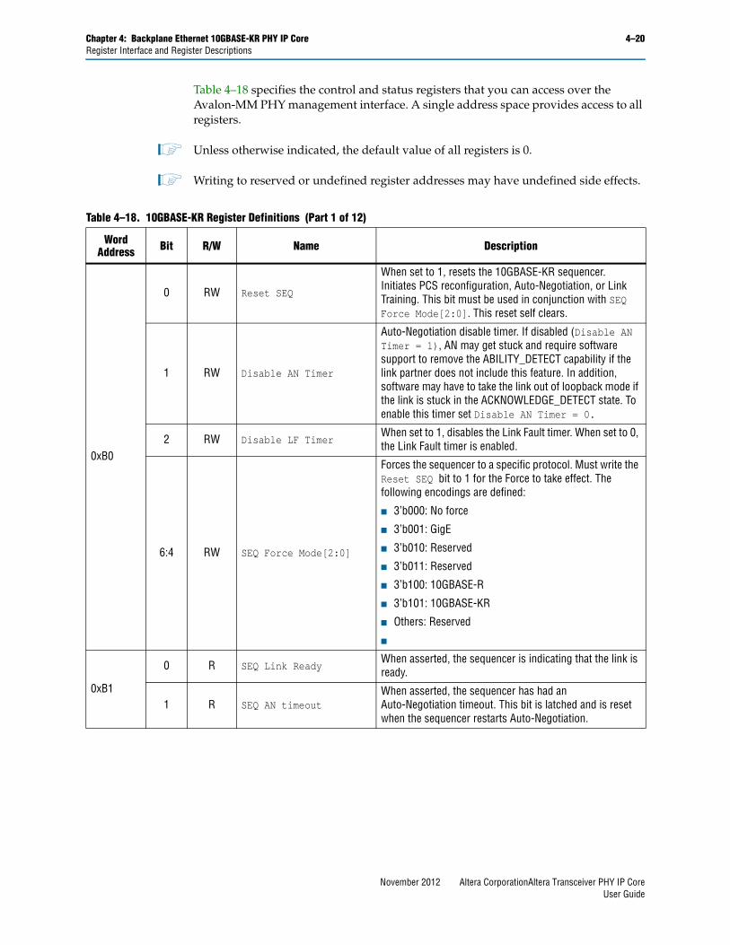
Chapter 4: Backplane Ethernet 10GBASE-KR PHY IP Core 4–20Register Interface and Register Descriptions
Table 4–18 specifies the control and status registers that you can access over the Avalon-MM PHY management interface. A single address space provides access to all registers.
1 Unless otherwise indicated, the default value of all registers is 0.
1 Writing to reserved or undefined register addresses may have undefined side effects.
Table 4–18. 10GBASE-KR Register Definitions (Part 1 of 12)
Word Address Bit R/W Name Description
0xB0
0 RW Reset SEQ
When set to 1, resets the 10GBASE-KR sequencer. Initiates PCS reconfiguration, Auto-Negotiation, or Link Training. This bit must be used in conjunction with SEQ Force Mode[2:0]. This reset self clears.
1 RW Disable AN Timer
Auto-Negotiation disable timer. If disabled (Disable AN Timer = 1), AN may get stuck and require software support to remove the ABILITY_DETECT capability if the link partner does not include this feature. In addition, software may have to take the link out of loopback mode if the link is stuck in the ACKNOWLEDGE_DETECT state. To enable this timer set Disable AN Timer = 0.
2 RW Disable LF TimerWhen set to 1, disables the Link Fault timer. When set to 0, the Link Fault timer is enabled.
6:4 RW SEQ Force Mode[2:0]
Forces the sequencer to a specific protocol. Must write the Reset SEQ bit to 1 for the Force to take effect. The following encodings are defined:
■ 3’b000: No force
■ 3’b001: GigE
■ 3’b010: Reserved
■ 3’b011: Reserved
■ 3’b100: 10GBASE-R
■ 3’b101: 10GBASE-KR
■ Others: Reserved
■
0xB1
0 R SEQ Link ReadyWhen asserted, the sequencer is indicating that the link is ready.
1 R SEQ AN timeoutWhen asserted, the sequencer has had an Auto-Negotiation timeout. This bit is latched and is reset when the sequencer restarts Auto-Negotiation.
November 2012 Altera CorporationAltera Transceiver PHY IP CoreUser Guide
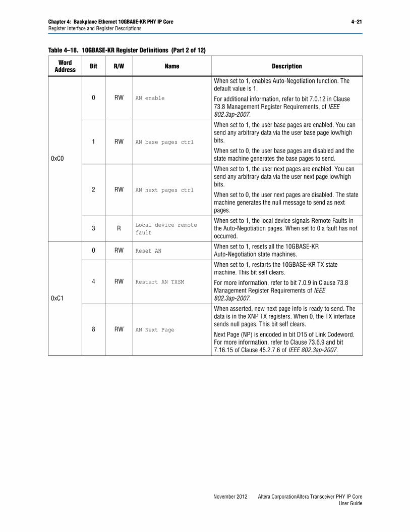
Chapter 4: Backplane Ethernet 10GBASE-KR PHY IP Core 4–21Register Interface and Register Descriptions
0xC0
0 RW AN enable
When set to 1, enables Auto-Negotiation function. The default value is 1.
For additional information, refer to bit 7.0.12 in Clause 73.8 Management Register Requirements, of IEEE 802.3ap-2007.
1 RW AN base pages ctrl
When set to 1, the user base pages are enabled. You can send any arbitrary data via the user base page low/high bits.
When set to 0, the user base pages are disabled and the state machine generates the base pages to send.
2 RW AN next pages ctrl
When set to 1, the user next pages are enabled. You can send any arbitrary data via the user next page low/high bits.
When set to 0, the user next pages are disabled. The state machine generates the null message to send as next pages.
3 R Local device remote fault
When set to 1, the local device signals Remote Faults in the Auto-Negotiation pages. When set to 0 a fault has not occurred.
0xC1
0 RW Reset ANWhen set to 1, resets all the 10GBASE-KR Auto-Negotiation state machines.
4 RW Restart AN TXSM
When set to 1, restarts the 10GBASE-KR TX state machine. This bit self clears.
For more information, refer to bit 7.0.9 in Clause 73.8 Management Register Requirements of IEEE 802.3ap-2007.
8 RW AN Next Page
When asserted, new next page info is ready to send. The data is in the XNP TX registers. When 0, the TX interface sends null pages. This bit self clears.
Next Page (NP) is encoded in bit D15 of Link Codeword. For more information, refer to Clause 73.6.9 and bit 7.16.15 of Clause 45.2.7.6 of IEEE 802.3ap-2007.
Table 4–18. 10GBASE-KR Register Definitions (Part 2 of 12)
Word Address Bit R/W Name Description
November 2012 Altera CorporationAltera Transceiver PHY IP CoreUser Guide
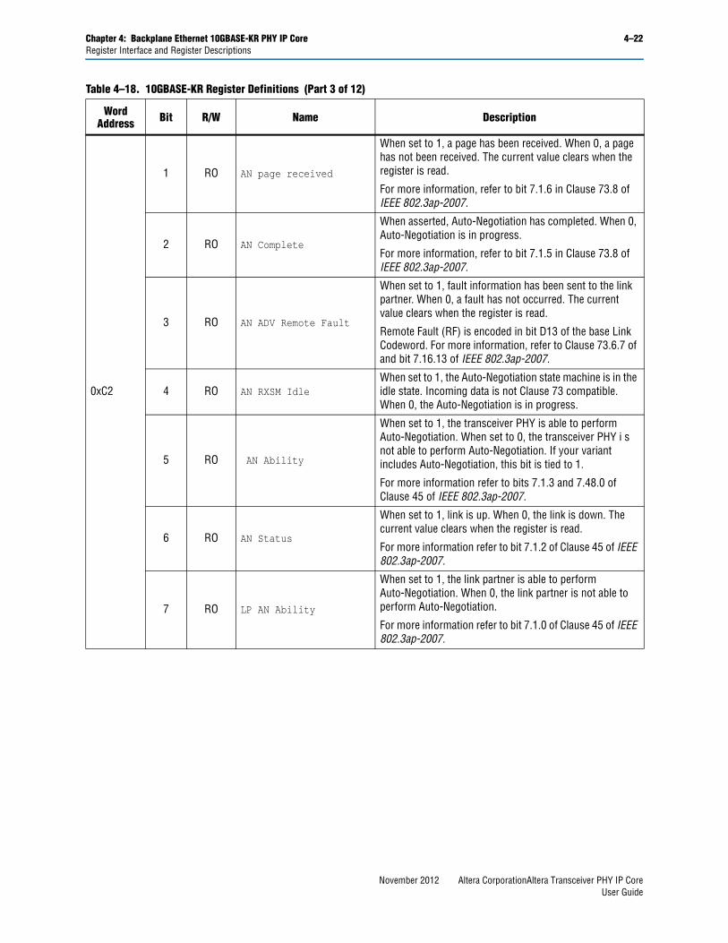
Chapter 4: Backplane Ethernet 10GBASE-KR PHY IP Core 4–22Register Interface and Register Descriptions
0xC2
1 RO AN page received
When set to 1, a page has been received. When 0, a page has not been received. The current value clears when the register is read.
For more information, refer to bit 7.1.6 in Clause 73.8 of IEEE 802.3ap-2007.
2 RO AN Complete
When asserted, Auto-Negotiation has completed. When 0, Auto-Negotiation is in progress.
For more information, refer to bit 7.1.5 in Clause 73.8 of IEEE 802.3ap-2007.
3 RO AN ADV Remote Fault
When set to 1, fault information has been sent to the link partner. When 0, a fault has not occurred. The current value clears when the register is read.
Remote Fault (RF) is encoded in bit D13 of the base Link Codeword. For more information, refer to Clause 73.6.7 of and bit 7.16.13 of IEEE 802.3ap-2007.
4 RO AN RXSM IdleWhen set to 1, the Auto-Negotiation state machine is in the idle state. Incoming data is not Clause 73 compatible. When 0, the Auto-Negotiation is in progress.
5 RO AN Ability
When set to 1, the transceiver PHY is able to perform Auto-Negotiation. When set to 0, the transceiver PHY i s not able to perform Auto-Negotiation. If your variant includes Auto-Negotiation, this bit is tied to 1.
For more information refer to bits 7.1.3 and 7.48.0 of Clause 45 of IEEE 802.3ap-2007.
6 RO AN Status
When set to 1, link is up. When 0, the link is down. The current value clears when the register is read.
For more information refer to bit 7.1.2 of Clause 45 of IEEE 802.3ap-2007.
7 RO LP AN Ability
When set to 1, the link partner is able to perform Auto-Negotiation. When 0, the link partner is not able to perform Auto-Negotiation.
For more information refer to bit 7.1.0 of Clause 45 of IEEE 802.3ap-2007.
Table 4–18. 10GBASE-KR Register Definitions (Part 3 of 12)
Word Address Bit R/W Name Description
November 2012 Altera CorporationAltera Transceiver PHY IP CoreUser Guide
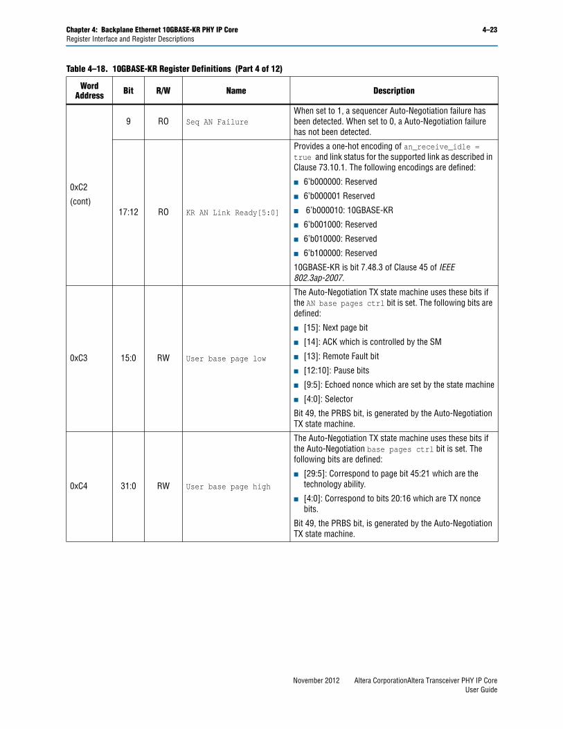
Chapter 4: Backplane Ethernet 10GBASE-KR PHY IP Core 4–23Register Interface and Register Descriptions
0xC2
(cont)
9 RO Seq AN FailureWhen set to 1, a sequencer Auto-Negotiation failure has been detected. When set to 0, a Auto-Negotiation failure has not been detected.
17:12 RO KR AN Link Ready[5:0]
Provides a one-hot encoding of an_receive_idle = true and link status for the supported link as described in Clause 73.10.1. The following encodings are defined:
■ 6’b000000: Reserved
■ 6’b000001 Reserved
■ 6’b000010: 10GBASE-KR
■ 6’b001000: Reserved
■ 6’b010000: Reserved
■ 6’b100000: Reserved
10GBASE-KR is bit 7.48.3 of Clause 45 of IEEE 802.3ap-2007.
0xC3 15:0 RW User base page low
The Auto-Negotiation TX state machine uses these bits if the AN base pages ctrl bit is set. The following bits are defined:
■ [15]: Next page bit
■ [14]: ACK which is controlled by the SM
■ [13]: Remote Fault bit
■ [12:10]: Pause bits
■ [9:5]: Echoed nonce which are set by the state machine
■ [4:0]: Selector
Bit 49, the PRBS bit, is generated by the Auto-Negotiation TX state machine.
0xC4 31:0 RW User base page high
The Auto-Negotiation TX state machine uses these bits if the Auto-Negotiation base pages ctrl bit is set. The following bits are defined:
■ [29:5]: Correspond to page bit 45:21 which are the technology ability.
■ [4:0]: Correspond to bits 20:16 which are TX nonce bits.
Bit 49, the PRBS bit, is generated by the Auto-Negotiation TX state machine.
Table 4–18. 10GBASE-KR Register Definitions (Part 4 of 12)
Word Address Bit R/W Name Description
November 2012 Altera CorporationAltera Transceiver PHY IP CoreUser Guide
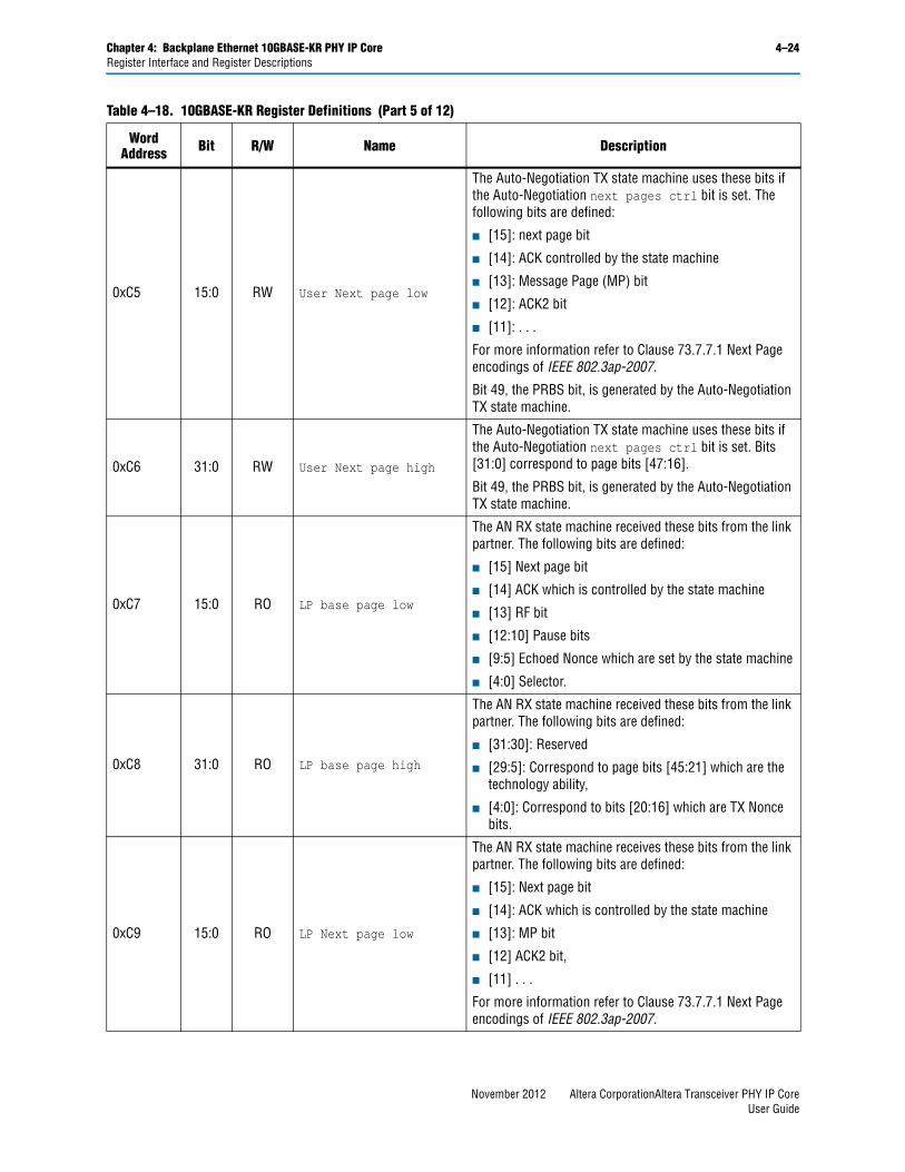
Chapter 4: Backplane Ethernet 10GBASE-KR PHY IP Core 4–24Register Interface and Register Descriptions
0xC5 15:0 RW User Next page low
The Auto-Negotiation TX state machine uses these bits if the Auto-Negotiation next pages ctrl bit is set. The following bits are defined:
■ [15]: next page bit
■ [14]: ACK controlled by the state machine
■ [13]: Message Page (MP) bit
■ [12]: ACK2 bit
■ [11]: . . .
For more information refer to Clause 73.7.7.1 Next Page encodings of IEEE 802.3ap-2007.
Bit 49, the PRBS bit, is generated by the Auto-Negotiation TX state machine.
0xC6 31:0 RW User Next page high
The Auto-Negotiation TX state machine uses these bits if the Auto-Negotiation next pages ctrl bit is set. Bits [31:0] correspond to page bits [47:16].
Bit 49, the PRBS bit, is generated by the Auto-Negotiation TX state machine.
0xC7 15:0 RO LP base page low
The AN RX state machine received these bits from the link partner. The following bits are defined:
■ [15] Next page bit
■ [14] ACK which is controlled by the state machine
■ [13] RF bit
■ [12:10] Pause bits
■ [9:5] Echoed Nonce which are set by the state machine
■ [4:0] Selector.
0xC8 31:0 RO LP base page high
The AN RX state machine received these bits from the link partner. The following bits are defined:
■ [31:30]: Reserved
■ [29:5]: Correspond to page bits [45:21] which are the technology ability,
■ [4:0]: Correspond to bits [20:16] which are TX Nonce bits.
0xC9 15:0 RO LP Next page low
The AN RX state machine receives these bits from the link partner. The following bits are defined:
■ [15]: Next page bit
■ [14]: ACK which is controlled by the state machine
■ [13]: MP bit
■ [12] ACK2 bit,
■ [11] . . .
For more information refer to Clause 73.7.7.1 Next Page encodings of IEEE 802.3ap-2007.
Table 4–18. 10GBASE-KR Register Definitions (Part 5 of 12)
Word Address Bit R/W Name Description
November 2012 Altera CorporationAltera Transceiver PHY IP CoreUser Guide
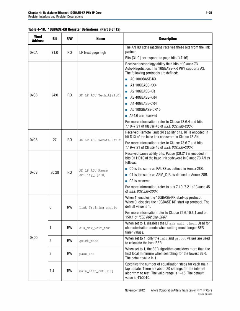
Chapter 4: Backplane Ethernet 10GBASE-KR PHY IP Core 4–25Register Interface and Register Descriptions
0xCA 31:0 RO LP Next page highThe AN RX state machine receives these bits from the link partner.
Bits [31:0] correspond to page bits [47:16]
0xCB 24:0 RO AN LP ADV Tech_A[24:0]
Received technology ability field bits of Clause 73 Auto-Negotiation. The 10GBASE-KR PHY supports A2. The following protocols are defined:
■ A0 1000BASE-KX
■ A1 10GBASE-KX4
■ A2 10GBASE-KR
■ A3 40GBASE-KR4
■ A4 40GBASE-CR4
■ A5 100GBASE-CR10
■ A24:6 are reserved
For more information, refer to Clause 73.6.4 and bits 7.19–7.21 of Clause 45 of IEEE 802.3ap-2007.
0xCB 27 RO AN LP ADV Remote Fault
Received Remote Fault (RF) ability bits. RF is encoded in bit D13 of the base link codeword in Clause 73 AN.
For more information, refer to Clause 73.6.7 and bits 7.19–7.21 of Clause 45 of IEEE 802.3ap-2007.
0xCB 30:28 RO AN LP ADV Pause Ability_C[2:0]
Received pause ability bits. Pause (C0:C1) is encoded in bits D11:D10 of the base link codeword in Clause 73 AN as follows:
■ C0 is the same as PAUSE as defined in Annex 28B.
■ C1 is the same as ASM_DIR as defined in Annex 28B.
■ C2 is reserved
For more information, refer to bits 7.19–7.21 of Clause 45 of IEEE 802.3ap-2007.
0xD0
0 RW Link Training enable
When 1, enables the 10GBASE-KR start-up protocol. When 0, disables the 10GBASE-KR start-up protocol. The default value is 1.
For more information refer to Clause 72.6.10.3.1 and bit 150.1 of IEEE 802.3ap-2007.
1 RW dis_max_wait_tmrWhen set to 1, disables the LT max_wait_timer. Used for characterization mode when setting much longer BER timer values.
2 RW quick_modeWhen set to 1, only the init and preset values are used to calculate the best BER.
3 RW pass_oneWhen set to 1, the BER algorithm considers more than the first local minimum when searching for the lowest BER. The default value is 1.
7:4 RW main_step_cnt[3:0]
Specifies the number of equalization steps for each main tap update. There are about 20 settings for the internal algorithm to test. The valid range is 1–15. The default value is 4’b0010.
Table 4–18. 10GBASE-KR Register Definitions (Part 6 of 12)
Word Address Bit R/W Name Description
November 2012 Altera CorporationAltera Transceiver PHY IP CoreUser Guide
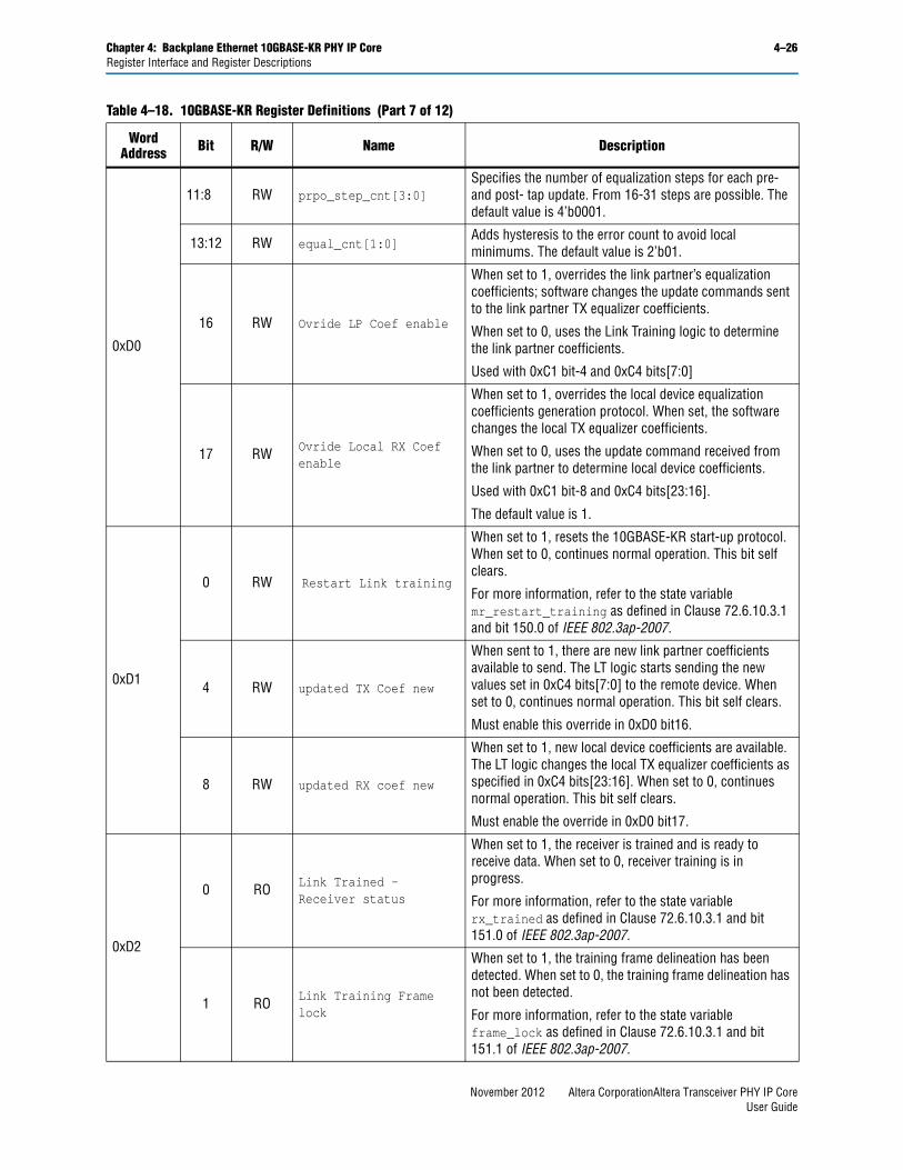
Chapter 4: Backplane Ethernet 10GBASE-KR PHY IP Core 4–26Register Interface and Register Descriptions
0xD0
11:8 RW prpo_step_cnt[3:0]Specifies the number of equalization steps for each pre- and post- tap update. From 16-31 steps are possible. The default value is 4’b0001.
13:12 RW equal_cnt[1:0]Adds hysteresis to the error count to avoid local minimums. The default value is 2’b01.
16 RW Ovride LP Coef enable
When set to 1, overrides the link partner’s equalization coefficients; software changes the update commands sent to the link partner TX equalizer coefficients.
When set to 0, uses the Link Training logic to determine the link partner coefficients.
Used with 0xC1 bit-4 and 0xC4 bits[7:0]
17 RW Ovride Local RX Coef enable
When set to 1, overrides the local device equalization coefficients generation protocol. When set, the software changes the local TX equalizer coefficients.
When set to 0, uses the update command received from the link partner to determine local device coefficients.
Used with 0xC1 bit-8 and 0xC4 bits[23:16].
The default value is 1.
0xD1
0 RW Restart Link training
When set to 1, resets the 10GBASE-KR start-up protocol. When set to 0, continues normal operation. This bit self clears.
For more information, refer to the state variable mr_restart_training as defined in Clause 72.6.10.3.1 and bit 150.0 of IEEE 802.3ap-2007.
4 RW updated TX Coef new
When sent to 1, there are new link partner coefficients available to send. The LT logic starts sending the new values set in 0xC4 bits[7:0] to the remote device. When set to 0, continues normal operation. This bit self clears.
Must enable this override in 0xD0 bit16.
8 RW updated RX coef new
When set to 1, new local device coefficients are available. The LT logic changes the local TX equalizer coefficients as specified in 0xC4 bits[23:16]. When set to 0, continues normal operation. This bit self clears.
Must enable the override in 0xD0 bit17.
0xD2
0 RO Link Trained – Receiver status
When set to 1, the receiver is trained and is ready to receive data. When set to 0, receiver training is in progress.
For more information, refer to the state variable rx_trained as defined in Clause 72.6.10.3.1 and bit 151.0 of IEEE 802.3ap-2007.
1 RO Link Training Frame lock
When set to 1, the training frame delineation has been detected. When set to 0, the training frame delineation has not been detected.
For more information, refer to the state variable frame_lock as defined in Clause 72.6.10.3.1 and bit 151.1 of IEEE 802.3ap-2007.
Table 4–18. 10GBASE-KR Register Definitions (Part 7 of 12)
Word Address Bit R/W Name Description
November 2012 Altera CorporationAltera Transceiver PHY IP CoreUser Guide
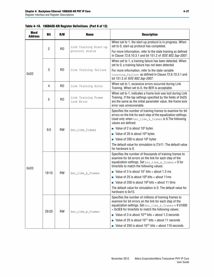
Chapter 4: Backplane Ethernet 10GBASE-KR PHY IP Core 4–27Register Interface and Register Descriptions
0xD2
2 RO Link Training Start-up protocol status
When set to 1, the start-up protocol is in progress. When set to 0, start-up protocol has completed.
For more information, refer to the state training as defined in Clause 72.6.10.3.1 and bit 151.2 of IEEE 802.3ap-2007.
3 RO Link Training failure
When set to 1, a training failure has been detected. When set to 0, a training failure has not been detected
For more information, refer to the state variable training_failure as defined in Clause 72.6.10.3.1 and bit 151.3 of IEEE 802.3ap-2007.
4 RO Link Training ErrorWhen set to 1, excessive errors occurred during Link Training. When set to 0, the BER is acceptable.
5 RO Link Training Frame lock Error
When set to 1, indicates a frame lock was lost during Link Training. If the tap settings specified by the fields of 0xD5 are the same as the initial parameter value, the frame lock error was unrecoverable.
0xD3
9:0 RW ber_time_frames
Specifies the number of training frames to examine for bit errors on the link for each step of the equalization settings. Used only when ber_time_k_frames is 0.The following values are defined:
■ Value of 2 is about 103 bytes
■ Value of 20 is about 104 bytes
■ Value of 200 is about 105 bytes
The default value for simulation is 2’b11. The default value for hardware is 0.
19:10 RW ber_time_k_frames
Specifies the number of thousands of training frames to examine for bit errors on the link for each step of the equalization settings. Set ber_time_m_frames = 0 for time/bits to match the following values:
■ Value of 3 is about 107 bits = about 1.3 ms
■ Value of 25 is about 108 bits = about 11ms
■ Value of 250 is about 109 bits = about 11 0ms
The default value for simulation is 0. The default value for hardware is 0x15.
29:20 RW ber_time_m_frames
Specifies the number of millions of training frames to examine for bit errors on the link for each step of the equalization settings. Set ber_time_k_frames = 4’d1000 = 0x3E8 for time/bits to match the following values:
■ Value of 3 is about 1010 bits = about 1.3 seconds
■ Value of 25 is about 1011 bits = about 11 seconds
■ Value of 250 is about 1012 bits = about 110 seconds
Table 4–18. 10GBASE-KR Register Definitions (Part 8 of 12)
Word Address Bit R/W Name Description
November 2012 Altera CorporationAltera Transceiver PHY IP CoreUser Guide
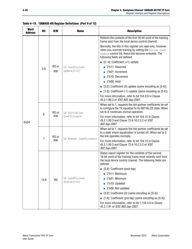
4–28 Chapter 4: Backplane Ethernet 10GBASE-KR PHY IP CoreRegister Interface and Register Descriptions
0xD4
5:0RO or
RWLD coefficient update[5:0]
Reflects the contents of the first 16-bit word of the training frame sent from the local device control channel.
Normally, the bits in this register are read-only; however, when you override training by setting the Ovride Coef enable control bit, these bits become writeable. The following fields are defined:
■ [5: 4]: Coefficient (+1) update
■ 2’b11: Reserved
■ 2’b01: Increment
■ 2’b10: Decrement
■ 2’b00: Hold
■ [3:2]: Coefficient (0) update (same encoding as [5:4])
■ [1:0]: Coefficient (-1) update (same encoding as [5:4])
For more information, refer to bit 154.5:0 in Clause 45.2.1.80.3 of IEEE 802.3ap-2007.
6 RO or RW
LD Initialize Coefficients
When set to 1, requests the link partner coefficients be set to configure the TX equalizer to its INITIALIZE state. When set to 0, continues normal operation.
For more information, refer to bit 154.12 in Clause 45.2.1.80.3 and Clause 72.6.10.2.3.2 of IEEE 802.3ap-2007.
7 RO or RW LD Preset Coefficients
When set to 1, requests the link partner coefficients be set to a state where equalization is turned off. When set to 0 the link operates normally.
For more information, refer to bit 154.13 in Clause 45.2.1.80.3 and Clause 72.6.10.2.3.2 of IEEE 802.3ap-2007.
13:8 RO LD coefficient status[5:0]
Status report register for the contents of the second, 16-bit word of the training frame most recently sent from the local device control channel. The following fields are defined:
■ [5:4]: Coefficient (post-tap)
■ 2’b11: Maximum
■ 2’b01: Minimum
■ 2’b10: Updated
■ 2’b00: Not updated
■ [3:2]: Coefficient (0) (same encoding as [5:4])
■ [1:0]: Coefficient (pre-tap) (same encoding as [5:4])
For more information, refer to bit 1.155.5:0 in Clause 45.2.1.81 of IEEE 802.3ap-2007.
Table 4–18. 10GBASE-KR Register Definitions (Part 9 of 12)
Word Address Bit R/W Name Description
Altera Transceiver PHY IP Core November 2012 Altera CorporationUser Guide
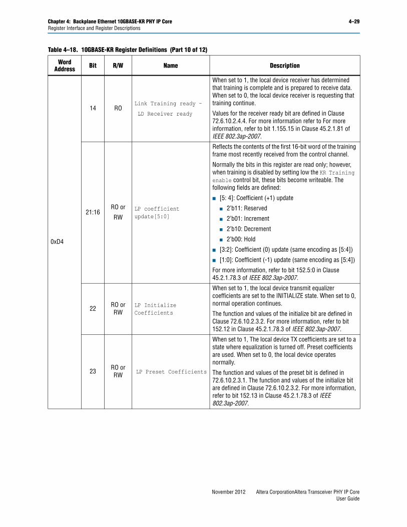
Chapter 4: Backplane Ethernet 10GBASE-KR PHY IP Core 4–29Register Interface and Register Descriptions
0xD4
14 ROLink Training ready –
LD Receiver ready
When set to 1, the local device receiver has determined that training is complete and is prepared to receive data. When set to 0, the local device receiver is requesting that training continue.
Values for the receiver ready bit are defined in Clause 72.6.10.2.4.4. For more information refer to For more information, refer to bit 1.155.15 in Clause 45.2.1.81 of IEEE 802.3ap-2007.
21:16RO or
RWLP coefficient update[5:0]
Reflects the contents of the first 16-bit word of the training frame most recently received from the control channel.
Normally the bits in this register are read only; however, when training is disabled by setting low the KR Training enable control bit, these bits become writeable. The following fields are defined:
■ [5: 4]: Coefficient (+1) update
■ 2’b11: Reserved
■ 2’b01: Increment
■ 2’b10: Decrement
■ 2’b00: Hold
■ [3:2]: Coefficient (0) update (same encoding as [5:4])
■ [1:0]: Coefficient (-1) update (same encoding as [5:4])
For more information, refer to bit 152.5:0 in Clause 45.2.1.78.3 of IEEE 802.3ap-2007.
22 RO or RW
LP Initialize Coefficients
When set to 1, the local device transmit equalizer coefficients are set to the INITIALIZE state. When set to 0, normal operation continues.
The function and values of the initialize bit are defined in Clause 72.6.10.2.3.2. For more information, refer to bit 152.12 in Clause 45.2.1.78.3 of IEEE 802.3ap-2007.
23 RO or RW LP Preset Coefficients
When set to 1, The local device TX coefficients are set to a state where equalization is turned off. Preset coefficients are used. When set to 0, the local device operates normally.
The function and values of the preset bit is defined in 72.6.10.2.3.1. The function and values of the initialize bit are defined in Clause 72.6.10.2.3.2. For more information, refer to bit 152.13 in Clause 45.2.1.78.3 of IEEE 802.3ap-2007.
Table 4–18. 10GBASE-KR Register Definitions (Part 10 of 12)
Word Address Bit R/W Name Description
November 2012 Altera CorporationAltera Transceiver PHY IP CoreUser Guide
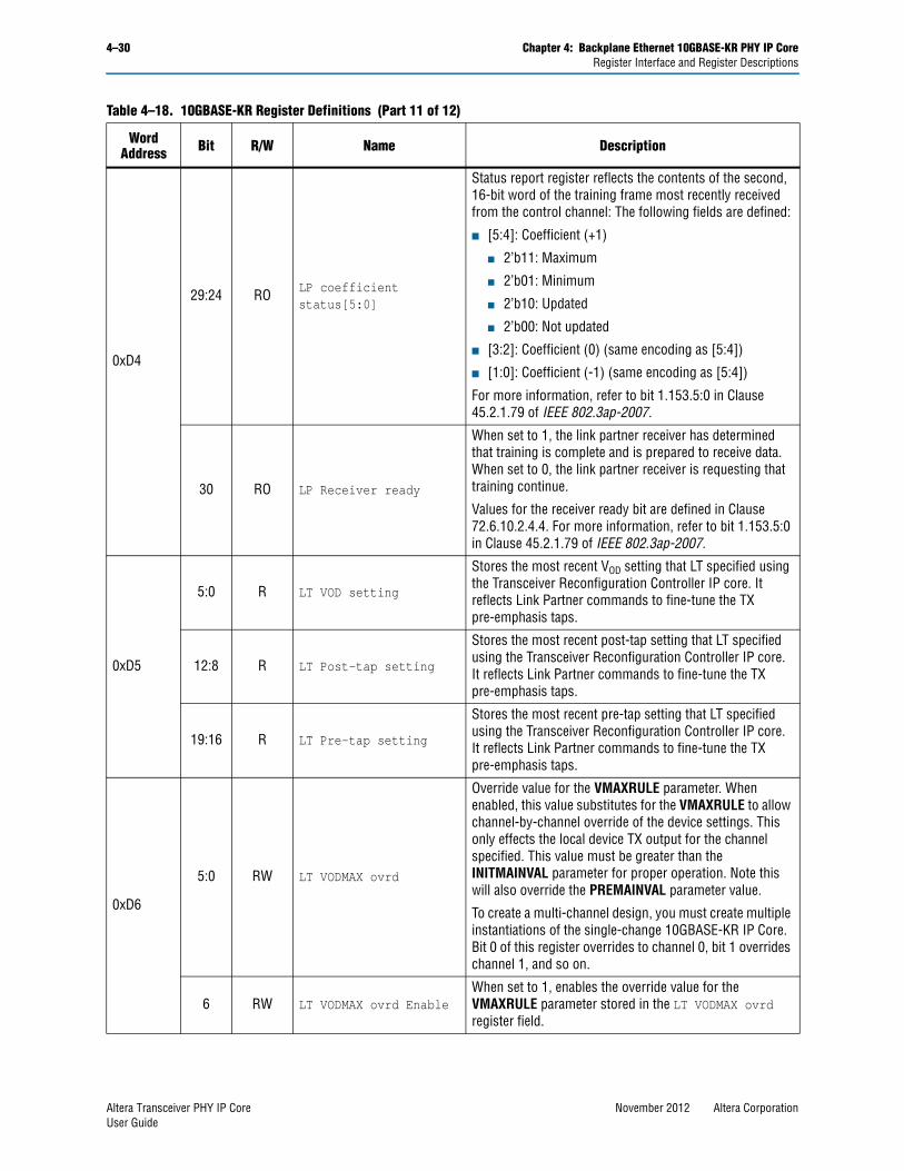
4–30 Chapter 4: Backplane Ethernet 10GBASE-KR PHY IP CoreRegister Interface and Register Descriptions
0xD4
29:24 RO LP coefficient status[5:0]
Status report register reflects the contents of the second, 16-bit word of the training frame most recently received from the control channel: The following fields are defined:
■ [5:4]: Coefficient (+1)
■ 2’b11: Maximum
■ 2’b01: Minimum
■ 2’b10: Updated
■ 2’b00: Not updated
■ [3:2]: Coefficient (0) (same encoding as [5:4])
■ [1:0]: Coefficient (-1) (same encoding as [5:4])
For more information, refer to bit 1.153.5:0 in Clause 45.2.1.79 of IEEE 802.3ap-2007.
30 RO LP Receiver ready
When set to 1, the link partner receiver has determined that training is complete and is prepared to receive data. When set to 0, the link partner receiver is requesting that training continue.
Values for the receiver ready bit are defined in Clause 72.6.10.2.4.4. For more information, refer to bit 1.153.5:0 in Clause 45.2.1.79 of IEEE 802.3ap-2007.
0xD5
5:0 R LT VOD setting
Stores the most recent VOD setting that LT specified using the Transceiver Reconfiguration Controller IP core. It reflects Link Partner commands to fine-tune the TX pre-emphasis taps.
12:8 R LT Post-tap setting
Stores the most recent post-tap setting that LT specified using the Transceiver Reconfiguration Controller IP core. It reflects Link Partner commands to fine-tune the TX pre-emphasis taps.
19:16 R LT Pre-tap setting
Stores the most recent pre-tap setting that LT specified using the Transceiver Reconfiguration Controller IP core. It reflects Link Partner commands to fine-tune the TX pre-emphasis taps.
0xD6
5:0 RW LT VODMAX ovrd
Override value for the VMAXRULE parameter. When enabled, this value substitutes for the VMAXRULE to allow channel-by-channel override of the device settings. This only effects the local device TX output for the channel specified. This value must be greater than the INITMAINVAL parameter for proper operation. Note this will also override the PREMAINVAL parameter value.
To create a multi-channel design, you must create multiple instantiations of the single-change 10GBASE-KR IP Core. Bit 0 of this register overrides to channel 0, bit 1 overrides channel 1, and so on.
6 RW LT VODMAX ovrd EnableWhen set to 1, enables the override value for the VMAXRULE parameter stored in the LT VODMAX ovrd register field.
Table 4–18. 10GBASE-KR Register Definitions (Part 11 of 12)
Word Address Bit R/W Name Description
Altera Transceiver PHY IP Core November 2012 Altera CorporationUser Guide
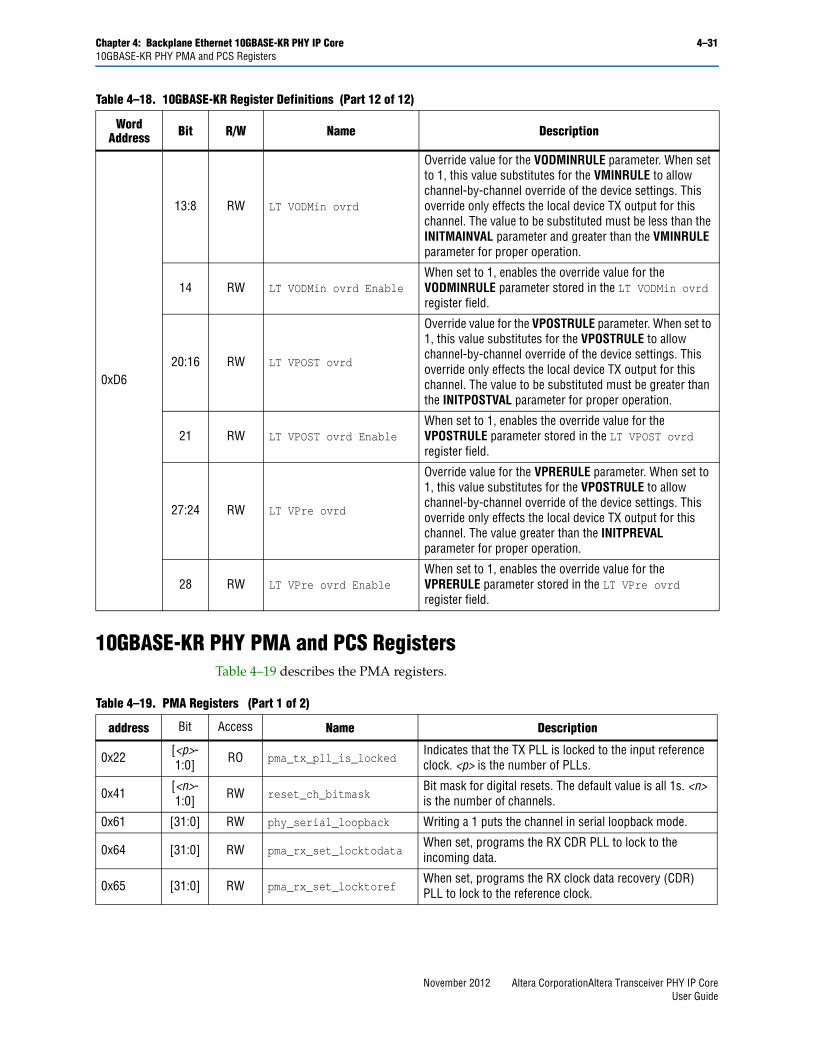
Chapter 4: Backplane Ethernet 10GBASE-KR PHY IP Core 4–3110GBASE-KR PHY PMA and PCS Registers
10GBASE-KR PHY PMA and PCS RegistersTable 4–19 describes the PMA registers.
0xD6
13:8 RW LT VODMin ovrd
Override value for the VODMINRULE parameter. When set to 1, this value substitutes for the VMINRULE to allow channel-by-channel override of the device settings. This override only effects the local device TX output for this channel. The value to be substituted must be less than the INITMAINVAL parameter and greater than the VMINRULE parameter for proper operation.
14 RW LT VODMin ovrd EnableWhen set to 1, enables the override value for the VODMINRULE parameter stored in the LT VODMin ovrd register field.
20:16 RW LT VPOST ovrd
Override value for the VPOSTRULE parameter. When set to 1, this value substitutes for the VPOSTRULE to allow channel-by-channel override of the device settings. This override only effects the local device TX output for this channel. The value to be substituted must be greater than the INITPOSTVAL parameter for proper operation.
21 RW LT VPOST ovrd EnableWhen set to 1, enables the override value for the VPOSTRULE parameter stored in the LT VPOST ovrd register field.
27:24 RW LT VPre ovrd
Override value for the VPRERULE parameter. When set to 1, this value substitutes for the VPOSTRULE to allow channel-by-channel override of the device settings. This override only effects the local device TX output for this channel. The value greater than the INITPREVAL parameter for proper operation.
28 RW LT VPre ovrd EnableWhen set to 1, enables the override value for the VPRERULE parameter stored in the LT VPre ovrd register field.
Table 4–18. 10GBASE-KR Register Definitions (Part 12 of 12)
Word Address Bit R/W Name Description
Table 4–19. PMA Registers (Part 1 of 2)
address Bit Access Name Description
0x22 [<p>-1:0] RO pma_tx_pll_is_locked
Indicates that the TX PLL is locked to the input reference clock. <p> is the number of PLLs.
0x41 [<n>-1:0] RW reset_ch_bitmask
Bit mask for digital resets. The default value is all 1s. <n> is the number of channels.
0x61 [31:0] RW phy_serial_loopback Writing a 1 puts the channel in serial loopback mode.
0x64 [31:0] RW pma_rx_set_locktodataWhen set, programs the RX CDR PLL to lock to the incoming data.
0x65 [31:0] RW pma_rx_set_locktorefWhen set, programs the RX clock data recovery (CDR) PLL to lock to the reference clock.
November 2012 Altera CorporationAltera Transceiver PHY IP CoreUser Guide
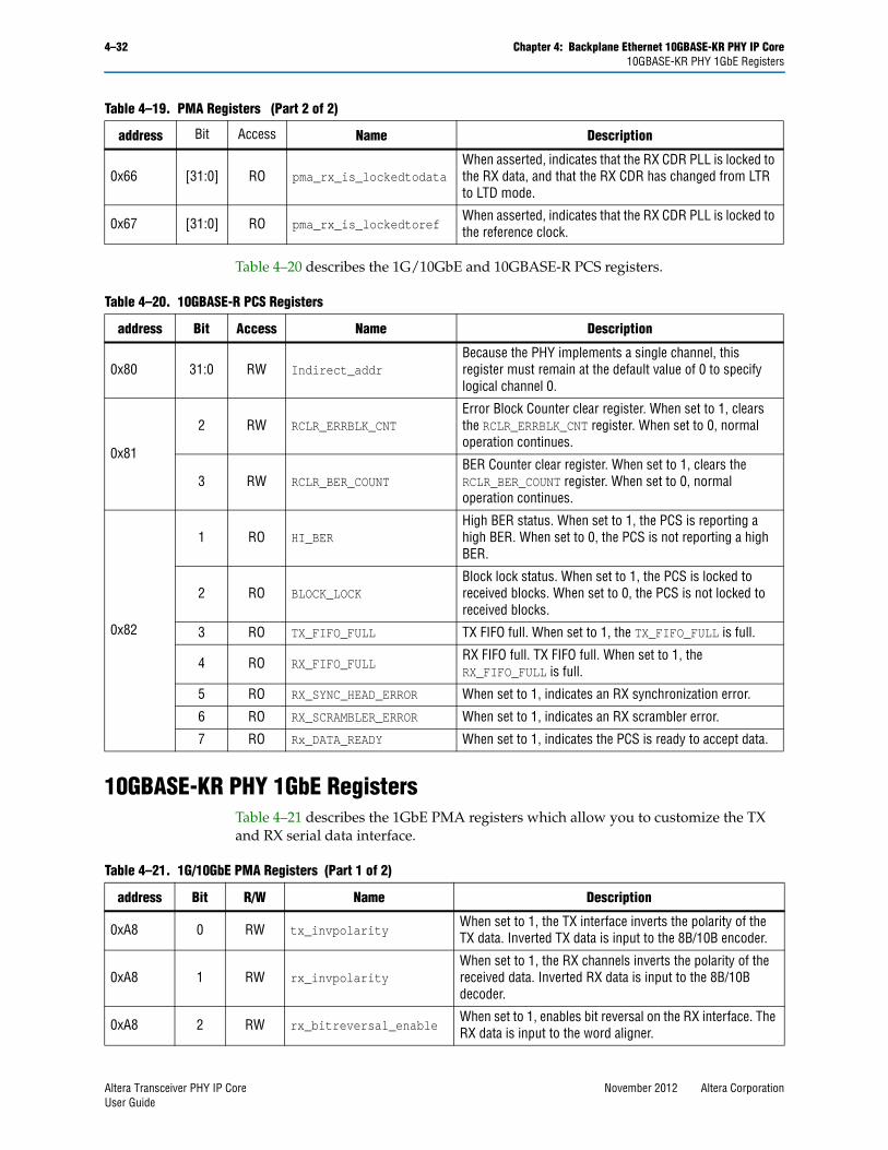
4–32 Chapter 4: Backplane Ethernet 10GBASE-KR PHY IP Core10GBASE-KR PHY 1GbE Registers
Table 4–20 describes the 1G/10GbE and 10GBASE-R PCS registers.
10GBASE-KR PHY 1GbE RegistersTable 4–21 describes the 1GbE PMA registers which allow you to customize the TX and RX serial data interface.
0x66 [31:0] RO pma_rx_is_lockedtodataWhen asserted, indicates that the RX CDR PLL is locked to the RX data, and that the RX CDR has changed from LTR to LTD mode.
0x67 [31:0] RO pma_rx_is_lockedtorefWhen asserted, indicates that the RX CDR PLL is locked to the reference clock.
Table 4–19. PMA Registers (Part 2 of 2)
address Bit Access Name Description
Table 4–20. 10GBASE-R PCS Registers
address Bit Access Name Description
0x80 31:0 RW Indirect_addrBecause the PHY implements a single channel, this register must remain at the default value of 0 to specify logical channel 0.
0x81
2 RW RCLR_ERRBLK_CNTError Block Counter clear register. When set to 1, clears the RCLR_ERRBLK_CNT register. When set to 0, normal operation continues.
3 RW RCLR_BER_COUNTBER Counter clear register. When set to 1, clears the RCLR_BER_COUNT register. When set to 0, normal operation continues.
0x82
1 RO HI_BERHigh BER status. When set to 1, the PCS is reporting a high BER. When set to 0, the PCS is not reporting a high BER.
2 RO BLOCK_LOCKBlock lock status. When set to 1, the PCS is locked to received blocks. When set to 0, the PCS is not locked to received blocks.
3 RO TX_FIFO_FULL TX FIFO full. When set to 1, the TX_FIFO_FULL is full.
4 RO RX_FIFO_FULLRX FIFO full. TX FIFO full. When set to 1, the RX_FIFO_FULL is full.
5 RO RX_SYNC_HEAD_ERROR When set to 1, indicates an RX synchronization error.
6 RO RX_SCRAMBLER_ERROR When set to 1, indicates an RX scrambler error.
7 RO Rx_DATA_READY When set to 1, indicates the PCS is ready to accept data.
Table 4–21. 1G/10GbE PMA Registers (Part 1 of 2)
address Bit R/W Name Description
0xA8 0 RW tx_invpolarityWhen set to 1, the TX interface inverts the polarity of the TX data. Inverted TX data is input to the 8B/10B encoder.
0xA8 1 RW rx_invpolarityWhen set to 1, the RX channels inverts the polarity of the received data. Inverted RX data is input to the 8B/10B decoder.
0xA8 2 RW rx_bitreversal_enableWhen set to 1, enables bit reversal on the RX interface. The RX data is input to the word aligner.
Altera Transceiver PHY IP Core November 2012 Altera CorporationUser Guide
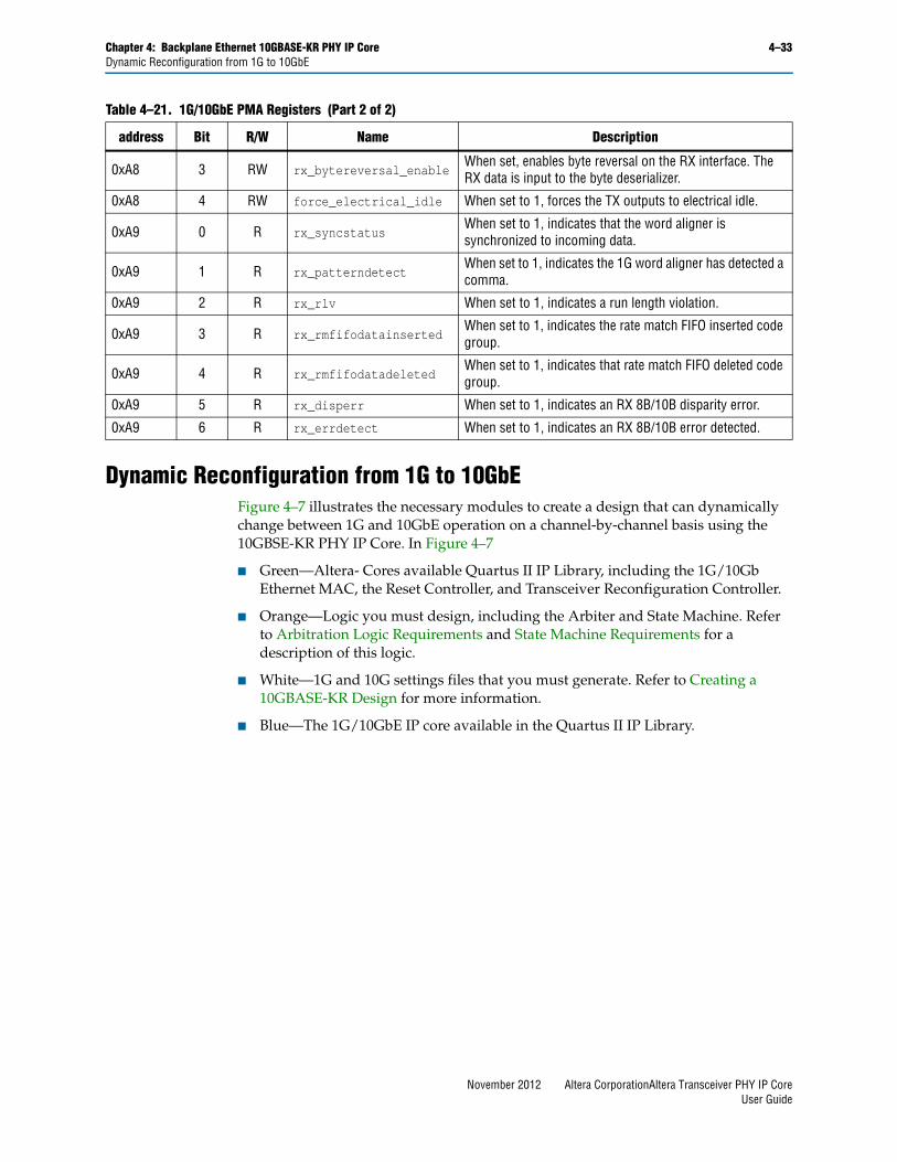
Chapter 4: Backplane Ethernet 10GBASE-KR PHY IP Core 4–33Dynamic Reconfiguration from 1G to 10GbE
Dynamic Reconfiguration from 1G to 10GbEFigure 4–7 illustrates the necessary modules to create a design that can dynamically change between 1G and 10GbE operation on a channel-by-channel basis using the 10GBSE-KR PHY IP Core. In Figure 4–7
■ Green—Altera- Cores available Quartus II IP Library, including the 1G/10Gb Ethernet MAC, the Reset Controller, and Transceiver Reconfiguration Controller.
■ Orange—Logic you must design, including the Arbiter and State Machine. Refer to Arbitration Logic Requirements and State Machine Requirements for a description of this logic.
■ White—1G and 10G settings files that you must generate. Refer to Creating a 10GBASE-KR Design for more information.
■ Blue—The 1G/10GbE IP core available in the Quartus II IP Library.
0xA8 3 RW rx_bytereversal_enableWhen set, enables byte reversal on the RX interface. The RX data is input to the byte deserializer.
0xA8 4 RW force_electrical_idle When set to 1, forces the TX outputs to electrical idle.
0xA9 0 R rx_syncstatusWhen set to 1, indicates that the word aligner is synchronized to incoming data.
0xA9 1 R rx_patterndetectWhen set to 1, indicates the 1G word aligner has detected a comma.
0xA9 2 R rx_rlv When set to 1, indicates a run length violation.
0xA9 3 R rx_rmfifodatainsertedWhen set to 1, indicates the rate match FIFO inserted code group.
0xA9 4 R rx_rmfifodatadeletedWhen set to 1, indicates that rate match FIFO deleted code group.
0xA9 5 R rx_disperr When set to 1, indicates an RX 8B/10B disparity error.
0xA9 6 R rx_errdetect When set to 1, indicates an RX 8B/10B error detected.
Table 4–21. 1G/10GbE PMA Registers (Part 2 of 2)
address Bit R/W Name Description
November 2012 Altera CorporationAltera Transceiver PHY IP CoreUser Guide
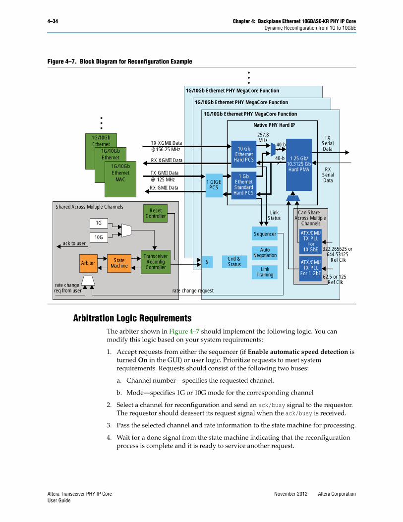
4–34 Chapter 4: Backplane Ethernet 10GBASE-KR PHY IP CoreDynamic Reconfiguration from 1G to 10GbE
Arbitration Logic RequirementsThe arbiter shown in Figure 4–7 should implement the following logic. You can modify this logic based on your system requirements:
1. Accept requests from either the sequencer (if Enable automatic speed detection is turned On in the GUI) or user logic. Prioritize requests to meet system requirements. Requests should consist of the following two buses:
a. Channel number—specifies the requested channel.
b. Mode—specifies 1G or 10G mode for the corresponding channel
2. Select a channel for reconfiguration and send an ack/busy signal to the requestor. The requestor should deassert its request signal when the ack/busy is received.
3. Pass the selected channel and rate information to the state machine for processing.
4. Wait for a done signal from the state machine indicating that the reconfiguration process is complete and it is ready to service another request.
Figure 4–7. Block Diagram for Reconfiguration Example
1G/10GbEthernet
MAC
1G/10Gb Ethernet PHY MegaCore Function
1G/10Gb Ethernet PHY MegaCore Function
1G/10Gb Ethernet PHY MegaCore Function
Native PHY Hard IP
257.8MHz
40-b
40-bTX
SerialData
RXSerialData
1.25 Gb/10.3125 GbHard PMA
LinkStatus
Sequencer
S
ResetController
StateMachineArbiter
rate change request
ack to user
rate change req from user
TransceiverReconfigController
AutoNegotiation
LinkTraining
10 GbEthernet
Hard PCS
Cntl & Status
RX GMII Data
TX GMII Data@ 125 MHz
RX XGMII Data
TX XGMII Data
Shared Across Multiple Channels
@156.25 MHz
1 GIGEPCS
1G/10GbEthernet
MAC1G/10GbEthernet
MAC
1G
10G
1 GbEthernetStandardHard PCS
322.265625 or644.53125
Ref Clk
62.5 or 125 Ref Clk
ATX/CMUTX PLL
For10 GbE
ATX/CMUTX PLL
For 1 GbE
Can Share Across Multiple
Channels
Altera Transceiver PHY IP Core November 2012 Altera CorporationUser Guide
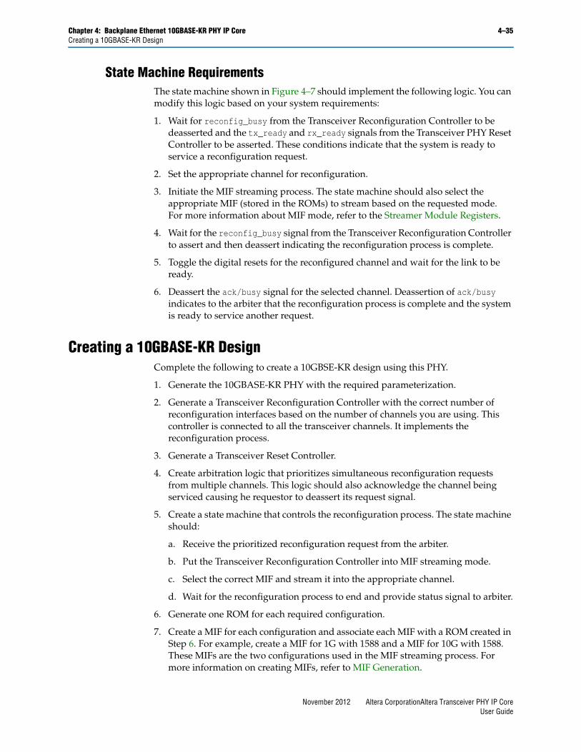
Chapter 4: Backplane Ethernet 10GBASE-KR PHY IP Core 4–35Creating a 10GBASE-KR Design
State Machine RequirementsThe state machine shown in Figure 4–7 should implement the following logic. You can modify this logic based on your system requirements:
1. Wait for reconfig_busy from the Transceiver Reconfiguration Controller to be deasserted and the tx_ready and rx_ready signals from the Transceiver PHY Reset Controller to be asserted. These conditions indicate that the system is ready to service a reconfiguration request.
2. Set the appropriate channel for reconfiguration.
3. Initiate the MIF streaming process. The state machine should also select the appropriate MIF (stored in the ROMs) to stream based on the requested mode. For more information about MIF mode, refer to the Streamer Module Registers.
4. Wait for the reconfig_busy signal from the Transceiver Reconfiguration Controller to assert and then deassert indicating the reconfiguration process is complete.
5. Toggle the digital resets for the reconfigured channel and wait for the link to be ready.
6. Deassert the ack/busy signal for the selected channel. Deassertion of ack/busy indicates to the arbiter that the reconfiguration process is complete and the system is ready to service another request.
Creating a 10GBASE-KR DesignComplete the following to create a 10GBSE-KR design using this PHY.
1. Generate the 10GBASE-KR PHY with the required parameterization.
2. Generate a Transceiver Reconfiguration Controller with the correct number of reconfiguration interfaces based on the number of channels you are using. This controller is connected to all the transceiver channels. It implements the reconfiguration process.
3. Generate a Transceiver Reset Controller.
4. Create arbitration logic that prioritizes simultaneous reconfiguration requests from multiple channels. This logic should also acknowledge the channel being serviced causing he requestor to deassert its request signal.
5. Create a state machine that controls the reconfiguration process. The state machine should:
a. Receive the prioritized reconfiguration request from the arbiter.
b. Put the Transceiver Reconfiguration Controller into MIF streaming mode.
c. Select the correct MIF and stream it into the appropriate channel.
d. Wait for the reconfiguration process to end and provide status signal to arbiter.
6. Generate one ROM for each required configuration.
7. Create a MIF for each configuration and associate each MIF with a ROM created in Step 6. For example, create a MIF for 1G with 1588 and a MIF for 10G with 1588. These MIFs are the two configurations used in the MIF streaming process. For more information on creating MIFs, refer to MIF Generation.
November 2012 Altera CorporationAltera Transceiver PHY IP CoreUser Guide
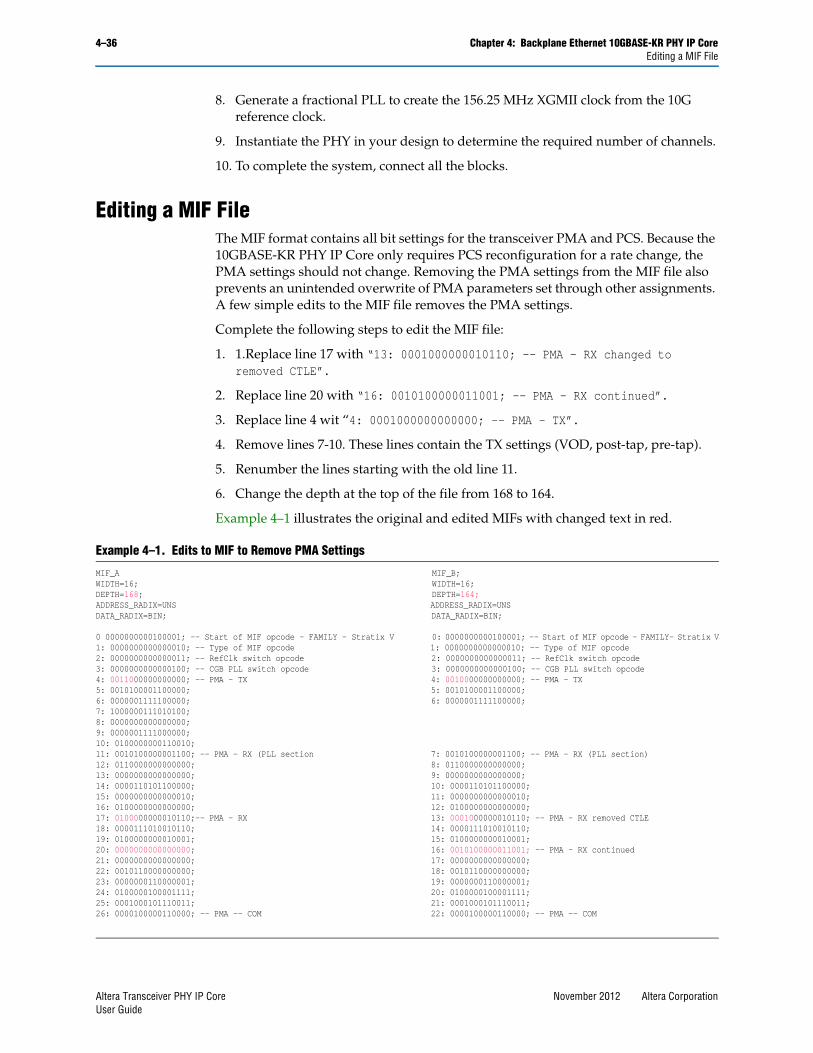
4–36 Chapter 4: Backplane Ethernet 10GBASE-KR PHY IP CoreEditing a MIF File
8. Generate a fractional PLL to create the 156.25 MHz XGMII clock from the 10G reference clock.
9. Instantiate the PHY in your design to determine the required number of channels.
10. To complete the system, connect all the blocks.
Editing a MIF FileThe MIF format contains all bit settings for the transceiver PMA and PCS. Because the 10GBASE-KR PHY IP Core only requires PCS reconfiguration for a rate change, the PMA settings should not change. Removing the PMA settings from the MIF file also prevents an unintended overwrite of PMA parameters set through other assignments. A few simple edits to the MIF file removes the PMA settings.
Complete the following steps to edit the MIF file:
1. 1.Replace line 17 with “13: 0001000000010110; -- PMA - RX changed to removed CTLE”.
2. Replace line 20 with “16: 0010100000011001; -- PMA - RX continued”.
3. Replace line 4 wit “4: 0001000000000000; -- PMA - TX”.
4. Remove lines 7-10. These lines contain the TX settings (VOD, post-tap, pre-tap).
5. Renumber the lines starting with the old line 11.
6. Change the depth at the top of the file from 168 to 164.
Example 4–1 illustrates the original and edited MIFs with changed text in red.
Example 4–1. Edits to MIF to Remove PMA Settings
MIF_A MIF_B;WIDTH=16; WIDTH=16;DEPTH=168; DEPTH=164;ADDRESS_RADIX=UNS ADDRESS_RADIX=UNSDATA_RADIX=BIN; DATA_RADIX=BIN;
0 0000000000100001; -- Start of MIF opcode - FAMILY - Stratix V 0: 0000000000100001; -- Start of MIF opcode - FAMILY- Stratix V1: 0000000000000010; -- Type of MIF opcode 1: 0000000000000010; -- Type of MIF opcode2: 0000000000000011; -- RefClk switch opcode 2: 0000000000000011; -- RefClk switch opcode3: 0000000000000100; -- CGB PLL switch opcode 3: 0000000000000100; -- CGB PLL switch opcode4: 0011000000000000; -- PMA - TX 4: 0010000000000000; -- PMA - TX5: 0010100001100000; 5: 0010100001100000;6: 0000001111100000; 6: 0000001111100000;7: 1000000111010100;8: 0000000000000000;9: 0000001111000000;10: 0100000000110010;11: 0010100000001100; -- PMA - RX (PLL section 7: 0010100000001100; -- PMA - RX (PLL section)12: 0110000000000000; 8: 0110000000000000; 13: 0000000000000000; 9: 0000000000000000;14: 0000110101100000; 10: 0000110101100000;15: 0000000000000010; 11: 0000000000000010;16: 0100000000000000; 12: 0100000000000000;17: 0100000000010110;-- PMA - RX 13: 0001000000010110; -- PMA - RX removed CTLE18: 0000111010010110; 14: 0000111010010110; 19: 0100000000010001; 15: 0100000000010001;20: 0000000000000000; 16: 0010100000011001; -- PMA - RX continued21: 0000000000000000; 17: 0000000000000000;22: 0010110000000000; 18: 0010110000000000;23: 0000000110000001; 19: 0000000110000001;24: 0100000100001111; 20: 0100000100001111; 25: 0001000101110011; 21: 0001000101110011;26: 0000100000110000; -- PMA -- COM 22: 0000100000110000; -- PMA -- COM
Altera Transceiver PHY IP Core November 2012 Altera CorporationUser Guide
Chapter 4: Backplane Ethernet 10GBASE-KR PHY IP Core 4–37Design Examples
Design ExamplesAltera has two design examples to assist you in integrating this PHY IP into your design.
■ A MAC and PHY design example. This design example instantiates the 1G/10GbE PHY IP along with the 1G/10G Ethernet MAC and supporting logic. It is part of the Quartus II 12.1 installation and is located in the <quartus2_install_dir>/ip subdirectory. For more information about this example design, refer to the 10-Gbps Ethernet MAC MegaCore Function User Guide.
■ A PHY-only design example. This design example instantiates the 1G/10GbE PHY IP along with its supporting logic as shown in Figure 4–7 above. It is available from Altera by request. To obtain this example design, please file a request through mySupport.
Dynamic Reconfiguration InterfaceTable 4–22 describes the signals the dynamic reconfiguration interface. This signals are illustrated in the 10GBASE-KR Top-Level Signals figure.
Table 4–22. Dynamic Reconfiguration Signals (Part 1 of 2)
Signal Name Direction Description
reconfig_to_xcvr[(<n>70-1):0]
InputReconfiguration signals from the Reconfiguration Design Example. <n> grows linearly with the number of reconfiguration interfaces.
reconfig_from_xcvr[(<n>46-1):0]
OUtputReconfiguration signals to the Reconfiguration Design Example. <n> grows linearly with the number of reconfiguration interfaces.
rc_busy Input When asserted, indicates that reconfig is in progress.
lt_start_rc Output When asserted, starts the TX PMA equalization reconfiguration.
main_rc[5:0] Output The main TX equalization tap value which is the same as VOD.
post_rc[4:0] Output The post-cursor TX equalization tap value.
pre_rc[3:0] Output The pre-cursor TX equalization tap value.
tap_to_upd[2:0] Output
Specifies the TX equalization tap to update to optimize signal quality. The following encodings are defined:
■ 3’b100: main tap
■ 3’b010: post-tap
■ 3’b001: pre-tap
seq_start_rc Output When asserted, starts PCS reconfiguration.
November 2012 Altera CorporationAltera Transceiver PHY IP CoreUser Guide
4–38 Chapter 4: Backplane Ethernet 10GBASE-KR PHY IP CoreAcronyms
AcronymsTable 4–23 lists commonly used acronyms for the 10GBASE-KR PHY IP Core.
pcs_mode_rc[5:0] Output
Specifies the PCS mode for reconfig using 1-hot encoding. The following modes are defined:
■ 6’b000001: Auto-Negotiation mode
■ 6’b000010: Link Training mode
■ 6’b000100: 10GBASE-KR data mode
■ 6’b001000: Reserved
■ 6’b010000: Reserved
■ 6’b100000: Reserved
mode_1g_10gbar Input This signal indicates the requested mode for the channel. A 1 indicates 1G mode and a 0 indicates 10G mode.
en_lcl_rxeq Output Enables RX Equalization. Equivalent to Link Trained status bit 0xD2 bit0. Active high.
rxeq_done Input
When asserted indicates that RX Equalization is complete.
This signal is ANDed with rx_trained from the 10GBASE-KR Training State Diagram. For more information, refer to Figure 72-5 in Clause 72.6.10.4.3 of IEEE 802.3ap-2007.
Table 4–22. Dynamic Reconfiguration Signals (Part 2 of 2)
Signal Name Direction Description
Table 4–23. Common Ethernet Acronyms (Part 1 of 2)
Acronym Definition
AN Auto-Negotiation in Ethernet as described in Clause 73 or of IEEE 802.3ap-2007.
BER Bit Error Rate.
DME Differential Manchester Encoding.
FEC Forward error correction.
GMII Gigabit Media Independent Interface.
KR Short hand notation for Backplane Ethernet with 64b/66b encoding.
LD Local Device.
LT Link training in backplane Ethernet Clause 72 for 10GBASE-KR and 40GBASE-KR4.
LP Link partner, to which the LD is connected.
MAC Media Access Control.
MII Media independent interface.
OSI Open System Interconnection.
PCS Physical Coding Sublayer.
PHY Physical Layer in OSI 7-layer architecture, also in Altera device scope is: PCS + PMA.
PMA Physical Medium Attachment.
PMD Physical Medium Dependent.
SGMII Serial Gigabit Media Independent Interface.
Altera Transceiver PHY IP Core November 2012 Altera CorporationUser Guide

Chapter 4: Backplane Ethernet 10GBASE-KR PHY IP Core 4–39Acronyms
WAN Wide Area Network.
XAUI 10 Gigabit Attachment Unit Interface.
Table 4–23. Common Ethernet Acronyms (Part 2 of 2)
Acronym Definition
November 2012 Altera CorporationAltera Transceiver PHY IP CoreUser Guide

4–40 Chapter 4: Backplane Ethernet 10GBASE-KR PHY IP CoreAcronyms
Altera Transceiver PHY IP Core November 2012 Altera CorporationUser Guide
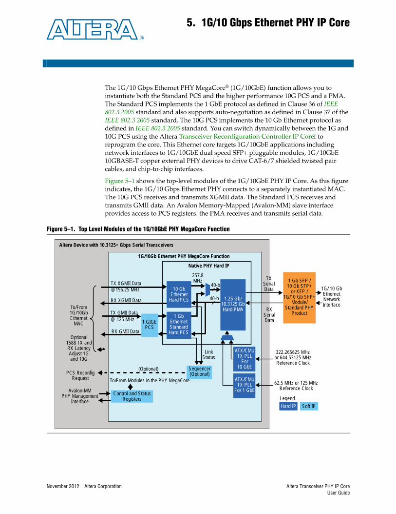
November 2012 Altera Corporation
5. 1G/10 Gbps Ethernet PHY IP Core
The 1G/10 Gbps Ethernet PHY MegaCore® (1G/10GbE) function allows you to instantiate both the Standard PCS and the higher performance 10G PCS and a PMA. The Standard PCS implements the 1 GbE protocol as defined in Clause 36 of IEEE 802.3 2005 standard and also supports auto-negotiation as defined in Clause 37 of the IEEE 802.3 2005 standard. The 10G PCS implements the 10 Gb Ethernet protocol as defined in IEEE 802.3 2005 standard. You can switch dynamically between the 1G and 10G PCS using the Altera Transceiver Reconfiguration Controller IP Coref to reprogram the core. This Ethernet core targets 1G/10GbE applications including network interfaces to 1G/10GbE dual speed SFP+ pluggable modules, 1G/10GbE 10GBASE-T copper external PHY devices to drive CAT-6/7 shielded twisted pair cables, and chip-to-chip interfaces.
Figure 5–1 shows the top-level modules of the 1G/10GbE PHY IP Core. As this figure indicates, the 1G/10 Gbps Ethernet PHY connects to a separately instantiated MAC. The 10G PCS receives and transmits XGMII data. The Standard PCS receives and transmits GMII data. An Avalon Memory-Mapped (Avalon-MM) slave interface provides access to PCS registers. the PMA receives and transmits serial data.
Figure 5–1. Top Level Modules of the 1G/10GbE PHY MegaCore Function
Altera Device with 10.3125+ Gbps Serial Transceivers
1G/10Gb Ethernet PHY MegaCore Function
Native PHY Hard IP
257.8MHz
40-b
40-bTX
SerialData
RXSerialData
1 Gb SFP /10 Gb SFP+
or XFP /1G/10 Gb SFP+
Module/Standard PHY
Product
1G/ 10 GbEthernetNetworkInterface
322.265625 MHzor 644.53125 MHzReference Clock
62.5 MHz or 125 MHzReference Clock
LegendHard IP Soft IP
ATX/CMUTX PLL
For10 GbE
ATX/CMUTX PLL
For 1 GbE
1.25 Gb/10.3125 GbHard PMA
LinkStatus
Sequencer(Optional)
10 GbEthernet
Hard PCS
1 GbEthernetStandardHard PCS
(Optional)
To/From Modules in the PHY MegaCore
Control and StatusRegisters
Avalon-MMPHY Management
Interface
PCS ReconfigRequest
Optional1588 TX andRX LatencyAdjust 1Gand 10G
To/From1G/10GbEthernet
MACRX GMII Data
TX GMII Data@ 125 MHz
RX XGMII Data
TX XGMII [email protected] MHz
1 GIGEPCS
Altera Transceiver PHY IP CoreUser Guide
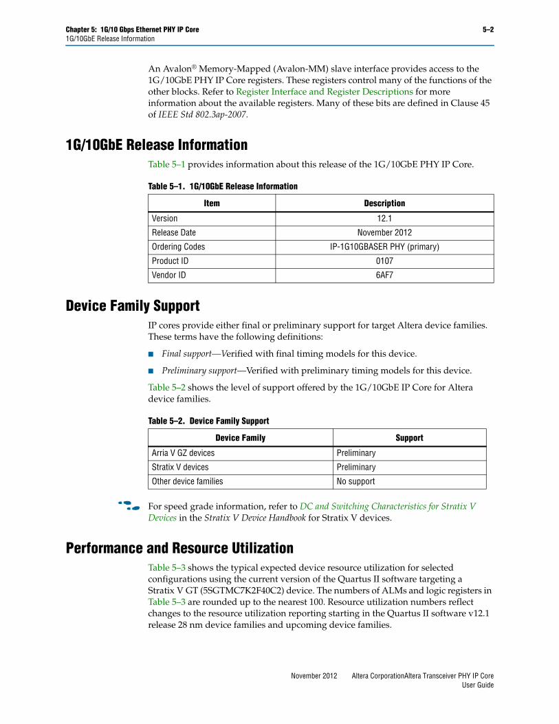
Chapter 5: 1G/10 Gbps Ethernet PHY IP Core 5–21G/10GbE Release Information
An Avalon® Memory-Mapped (Avalon-MM) slave interface provides access to the 1G/10GbE PHY IP Core registers. These registers control many of the functions of the other blocks. Refer to Register Interface and Register Descriptions for more information about the available registers. Many of these bits are defined in Clause 45 of IEEE Std 802.3ap-2007.
1G/10GbE Release InformationTable 5–1 provides information about this release of the 1G/10GbE PHY IP Core.
Device Family SupportIP cores provide either final or preliminary support for target Altera device families. These terms have the following definitions:
■ Final support—Verified with final timing models for this device.
■ Preliminary support—Verified with preliminary timing models for this device.
Table 5–2 shows the level of support offered by the 1G/10GbE IP Core for Altera device families.
f For speed grade information, refer to DC and Switching Characteristics for Stratix V Devices in the Stratix V Device Handbook for Stratix V devices.
Performance and Resource UtilizationTable 5–3 shows the typical expected device resource utilization for selected configurations using the current version of the Quartus II software targeting a Stratix V GT (5SGTMC7K2F40C2) device. The numbers of ALMs and logic registers in Table 5–3 are rounded up to the nearest 100. Resource utilization numbers reflect changes to the resource utilization reporting starting in the Quartus II software v12.1 release 28 nm device families and upcoming device families.
Table 5–1. 1G/10GbE Release Information
Item Description
Version 12.1
Release Date November 2012
Ordering Codes IP-1G10GBASER PHY (primary)
Product ID 0107
Vendor ID 6AF7
Table 5–2. Device Family Support
Device Family Support
Arria V GZ devices Preliminary
Stratix V devices Preliminary
Other device families No support
November 2012 Altera CorporationAltera Transceiver PHY IP CoreUser Guide
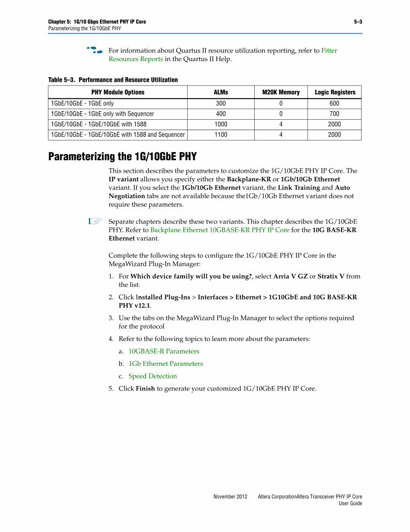
Chapter 5: 1G/10 Gbps Ethernet PHY IP Core 5–3Parameterizing the 1G/10GbE PHY
f For information about Quartus II resource utilization reporting, refer to Fitter Resources Reports in the Quartus II Help.
Parameterizing the 1G/10GbE PHYThis section describes the parameters to customize the 1G/10GbE PHY IP Core. The IP variant allows you specify either the Backplane-KR or 1Gb/10Gb Ethernet variant. If you select the 1Gb/10Gb Ethernet variant, the Link Training and Auto Negotiation tabs are not available because the1Gb/10Gb Ethernet variant does not require these parameters.
1 Separate chapters describe these two variants. This chapter describes the 1G/10GbE PHY. Refer to Backplane Ethernet 10GBASE-KR PHY IP Core for the 10G BASE-KR Ethernet variant.
Complete the following steps to configure the 1G/10GbE PHY IP Core in the MegaWizard Plug-In Manager:
1. For Which device family will you be using?, select Arria V GZ or Stratix V from the list.
2. Click Installed Plug-Ins > Interfaces > Ethernet > 1G10GbE and 10G BASE-KR PHY v12.1.
3. Use the tabs on the MegaWizard Plug-In Manager to select the options required for the protocol
4. Refer to the following topics to learn more about the parameters:
a. 10GBASE-R Parameters
b. 1Gb Ethernet Parameters
c. Speed Detection
5. Click Finish to generate your customized 1G/10GbE PHY IP Core.
Table 5–3. Performance and Resource Utilization
PHY Module Options ALMs M20K Memory Logic Registers
1GbE/10GbE - 1GbE only 300 0 600
1GbE/10GbE - 1GbE only with Sequencer 400 0 700
1GbE/10GbE - 1GbE/10GbE with 1588 1000 4 2000
1GbE/10GbE - 1GbE/10GbE with 1588 and Sequencer 1100 4 2000
November 2012 Altera CorporationAltera Transceiver PHY IP CoreUser Guide
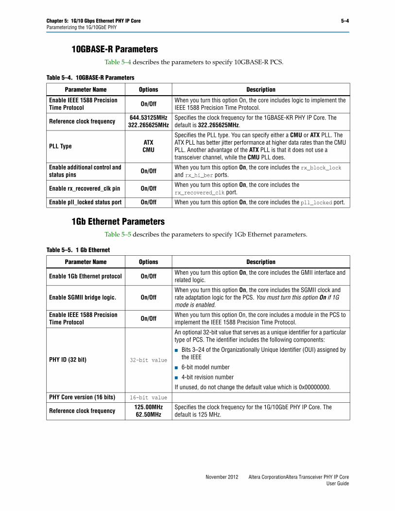
Chapter 5: 1G/10 Gbps Ethernet PHY IP Core 5–4Parameterizing the 1G/10GbE PHY
10GBASE-R ParametersTable 5–4 describes the parameters to specify 10GBASE-R PCS.
1Gb Ethernet ParametersTable 5–5 describes the parameters to specify 1Gb Ethernet parameters.
Table 5–4. 10GBASE-R Parameters
Parameter Name Options Description
Enable IEEE 1588 Precision Time Protocol On/Off When you turn this option On, the core includes logic to implement the
IEEE 1588 Precision Time Protocol.
Reference clock frequency 644.53125MHz 322.265625MHz
Specifies the clock frequency for the 1GBASE-KR PHY IP Core. The default is 322.265625MHz.
PLL Type ATXCMU
Specifies the PLL type. You can specify either a CMU or ATX PLL. The ATX PLL has better jitter performance at higher data rates than the CMU PLL. Another advantage of the ATX PLL is that it does not use a transceiver channel, while the CMU PLL does.
Enable additional control and status pins On/Off When you turn this option On, the core includes the rx_block_lock
and rx_hi_ber ports.
Enable rx_recovered_clk pin On/Off When you turn this option On, the core includes the rx_recovered_clk port.
Enable pll_locked status port On/Off When you turn this option On, the core includes the pll_locked port.
Table 5–5. 1 Gb Ethernet
Parameter Name Options Description
Enable 1Gb Ethernet protocol On/Off When you turn this option On, the core includes the GMII interface and related logic.
Enable SGMII bridge logic. On/OffWhen you turn this option On, the core includes the SGMII clock and rate adaptation logic for the PCS. You must turn this option On if 1G mode is enabled.
Enable IEEE 1588 Precision Time Protocol On/Off When you turn this option On, the core includes a module in the PCS to
implement the IEEE 1588 Precision Time Protocol.
PHY ID (32 bit) 32-bit value
An optional 32-bit value that serves as a unique identifier for a particular type of PCS. The identifier includes the following components:
■ Bits 3–24 of the Organizationally Unique Identifier (OUI) assigned by the IEEE
■ 6-bit model number
■ 4-bit revision number
If unused, do not change the default value which is 0x00000000.
PHY Core version (16 bits) 16-bit value
Reference clock frequency 125.00MHz 62.50MHz
Specifies the clock frequency for the 1G/10GbE PHY IP Core. The default is 125 MHz.
November 2012 Altera CorporationAltera Transceiver PHY IP CoreUser Guide
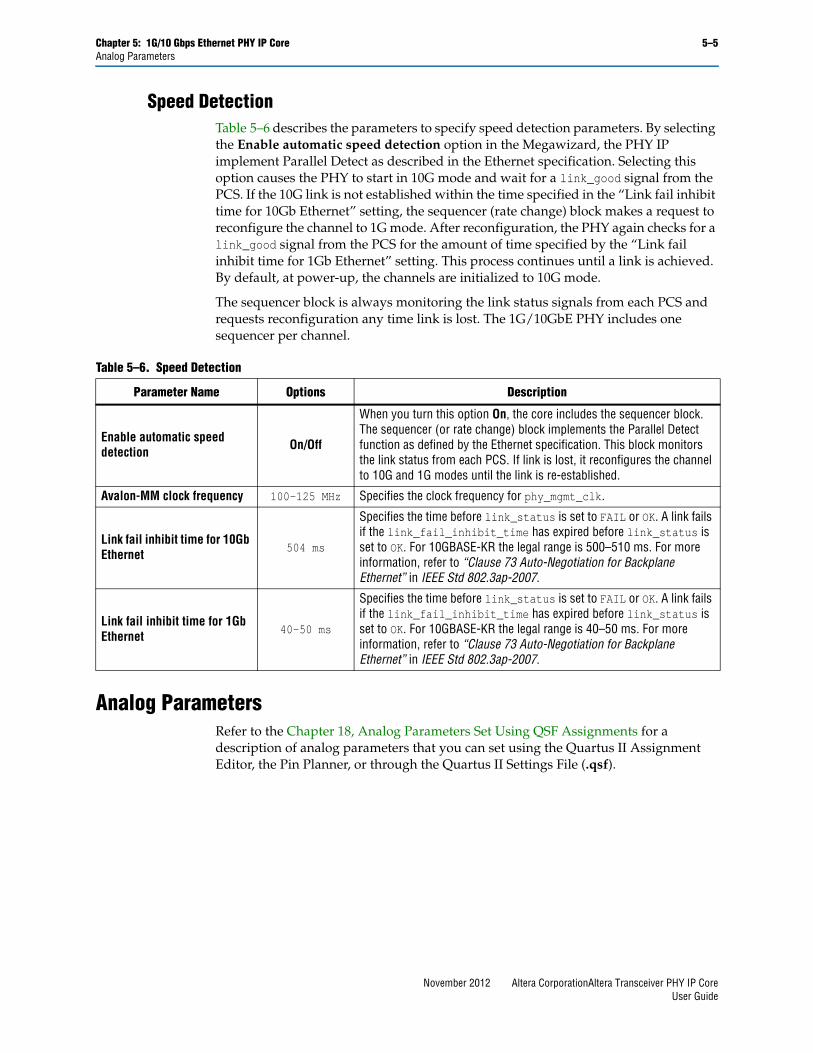
Chapter 5: 1G/10 Gbps Ethernet PHY IP Core 5–5Analog Parameters
Speed DetectionTable 5–6 describes the parameters to specify speed detection parameters. By selecting the Enable automatic speed detection option in the Megawizard, the PHY IP implement Parallel Detect as described in the Ethernet specification. Selecting this option causes the PHY to start in 10G mode and wait for a link_good signal from the PCS. If the 10G link is not established within the time specified in the “Link fail inhibit time for 10Gb Ethernet” setting, the sequencer (rate change) block makes a request to reconfigure the channel to 1G mode. After reconfiguration, the PHY again checks for a link_good signal from the PCS for the amount of time specified by the “Link fail inhibit time for 1Gb Ethernet” setting. This process continues until a link is achieved. By default, at power-up, the channels are initialized to 10G mode.
The sequencer block is always monitoring the link status signals from each PCS and requests reconfiguration any time link is lost. The 1G/10GbE PHY includes one sequencer per channel.
Analog ParametersRefer to the Chapter 18, Analog Parameters Set Using QSF Assignments for a description of analog parameters that you can set using the Quartus II Assignment Editor, the Pin Planner, or through the Quartus II Settings File (.qsf).
Table 5–6. Speed Detection
Parameter Name Options Description
Enable automatic speed detection On/Off
When you turn this option On, the core includes the sequencer block. The sequencer (or rate change) block implements the Parallel Detect function as defined by the Ethernet specification. This block monitors the link status from each PCS. If link is lost, it reconfigures the channel to 10G and 1G modes until the link is re-established.
Avalon-MM clock frequency 100–125 MHz Specifies the clock frequency for phy_mgmt_clk.
Link fail inhibit time for 10Gb Ethernet 504 ms
Specifies the time before link_status is set to FAIL or OK. A link fails if the link_fail_inhibit_time has expired before link_status is set to OK. For 10GBASE-KR the legal range is 500–510 ms. For more information, refer to “Clause 73 Auto-Negotiation for Backplane Ethernet” in IEEE Std 802.3ap-2007.
Link fail inhibit time for 1Gb Ethernet 40–50 ms
Specifies the time before link_status is set to FAIL or OK. A link fails if the link_fail_inhibit_time has expired before link_status is set to OK. For 10GBASE-KR the legal range is 40–50 ms. For more information, refer to “Clause 73 Auto-Negotiation for Backplane Ethernet” in IEEE Std 802.3ap-2007.
November 2012 Altera CorporationAltera Transceiver PHY IP CoreUser Guide
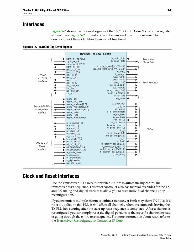
Chapter 5: 1G/10 Gbps Ethernet PHY IP Core 5–6Interfaces
InterfacesFigure 5–2 shows the top-level signals of the 1G/10GbE IP Core. Some of the signals shown in are Figure 5–2 unused and will be removed in a future release. The descriptions of these identifies them as not functional.
Clock and Reset InterfacesUse the Transceiver PHY Reset Controller IP Core to automatically control the transceiver reset sequence. This reset controller also has manual overrides for the TX and RX analog and digital circuits to allow you to reset individual channels upon reconfiguration.
If you instantiate multiple channels within a transceiver bank they share TX PLLs. If a reset is applied to this PLL, it will affect all channels. Altera recommends leaving the TX PLL free-running after the start-up reset sequence is completed. After a channel is reconfigured you can simply reset the digital portions of that specific channel instead of going through the entire reset sequence. For more information about reset, refer to the Transceiver Reconfiguration Controller IP Core.
Figure 5–2. 1G10GbE Top-Level Signals
xgmii_tx_dc[71:0]xgmii_tx_clkxgmii_rx_dc[71:0]xgmii_rx_clkgmii_tx_d[7:0]gmii_rx_d[7:0]gmii_tx_engmii_tx_errgmii_rx_errgmii_rx_dvled_char_errled_linkled_disp_errled_an
mgmt_clkmgmt_clk_resetmgmt_address[7:0]mgmt_writedata[31:0]mgmt_readdata[31:0]mgmt_writemgmt_readmgmt_waitrequest
rx_recovered_clktx_clkout_1gtx_clkout_10grx_clkout_1grx_clkout_10grx_coreclkin_1gtx_coreclkin_1gpll_ref_clk_1gpll_ref_clk_10gpll_powerdown_1gpll_powerdown_10gtx_analogresettx_digitalresetrx_analogresetrx_digitalresetusr_seq_reset
1G/10GbE Top-Level Signals
Reconfiguration
rx_serial_datatx_serial_data
reconfig_to_xcvr[(<n>70-1):0]reconfig_from_xcvr[(<n>46-1):0]
rc_busylt_start_rc
main_rc[5:0]post_rc[4:0]pre_rc[3:0]
tap_to_upd[2:0]seq_start_rc
pcs_mode_rc[5:0]mode_1g_10gbar
en_lcl_rxeqrxeq_done
rx_block_lockrx_hi_berpll_locked
rx_is_lockedtodatatx_cal_busyrx_cal_busycalc_clk_1g
rx_syncstatustx_pcfifo_error_1grx_pcfifo_error_1g
lcl_rftm_in_trigger[3:0]
tm_out_trigger[3:0]rx_rlv
rx_clksliprx_latency_adj_1g[11:0]tx_latency_adj_1g[11:0]
rx_latency_adj_10g[11:0]tx_latency_adj_10g[11:0]
rx_data_ready
TransceiverSerial Data
XGMIIand GMII Interfaces
Avalon-MM PHYManagement
Interface
Clocks andReset
Interface
Status
November 2012 Altera CorporationAltera Transceiver PHY IP CoreUser Guide
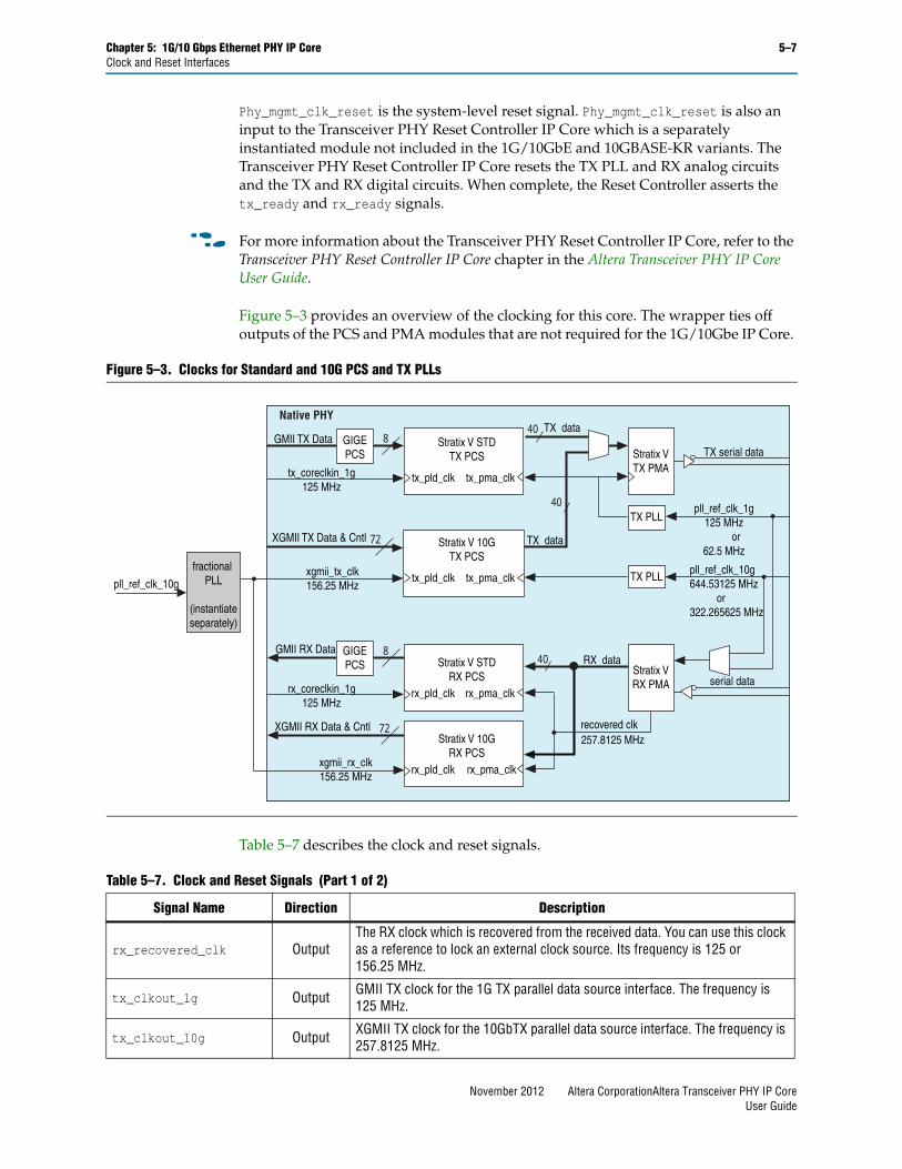
Chapter 5: 1G/10 Gbps Ethernet PHY IP Core 5–7Clock and Reset Interfaces
Phy_mgmt_clk_reset is the system-level reset signal. Phy_mgmt_clk_reset is also an input to the Transceiver PHY Reset Controller IP Core which is a separately instantiated module not included in the 1G/10GbE and 10GBASE-KR variants. The Transceiver PHY Reset Controller IP Core resets the TX PLL and RX analog circuits and the TX and RX digital circuits. When complete, the Reset Controller asserts the tx_ready and rx_ready signals.
f For more information about the Transceiver PHY Reset Controller IP Core, refer to the Transceiver PHY Reset Controller IP Core chapter in the Altera Transceiver PHY IP Core User Guide.
Figure 5–3 provides an overview of the clocking for this core. The wrapper ties off outputs of the PCS and PMA modules that are not required for the 1G/10Gbe IP Core.
Table 5–7 describes the clock and reset signals.
Figure 5–3. Clocks for Standard and 10G PCS and TX PLLs
xgmii_rx_clk156.25 MHz
xgmii_tx_clk156.25 MHz
Native PHY
Stratix V STDRX PCS
Stratix VTX PMAtx_coreclkin_1g
125 MHz
Stratix VRX PMA
TX PLL
TX PLL
40
rx_pld_clk rx_pma_clk
TX serial data8GMII TX Data
72XGMII TX Data & Cntl
RX data
40 TX data
40
TX data
serial data
pll_ref_clk_10g644.53125 MHz or 322.265625 MHz
pll_ref_clk_1g125 MHz or 62.5 MHz
Stratix V STDTX PCS
tx_pld_clk tx_pma_clk
8GMII RX Data
pll_ref_clk_10g
72XGMII RX Data & Cntl recovered clk257.8125 MHz
rx_coreclkin_1g125 MHz
Stratix V 10GRX PCS
rx_pld_clk rx_pma_clk
Stratix V 10GTX PCS
tx_pld_clk tx_pma_clkfractional
PLL
(instantiateseparately)
GIGEPCS
GIGEPCS
Table 5–7. Clock and Reset Signals (Part 1 of 2)
Signal Name Direction Description
rx_recovered_clk OutputThe RX clock which is recovered from the received data. You can use this clock as a reference to lock an external clock source. Its frequency is 125 or 156.25 MHz.
tx_clkout_1g Output GMII TX clock for the 1G TX parallel data source interface. The frequency is 125 MHz.
tx_clkout_10g Output XGMII TX clock for the 10GbTX parallel data source interface. The frequency is 257.8125 MHz.
November 2012 Altera CorporationAltera Transceiver PHY IP CoreUser Guide
Chapter 5: 1G/10 Gbps Ethernet PHY IP Core 5–8Data Interfaces
Data Interfaces Table 5–8 describes the signals in the XGMII and GMII interfaces. The MAC drives the TX XGMII and GMII signals to the 1G/10GbE PHY. The 1G/10GbE PHY drives to the RX XGMII or GMII signals to the MAC.
rx_clkout_1g Output GMII RX clock for the 1G RX parallel data source interface. The frequency is 125 MHz.
rx_clkout_10g Output XGMII RX clock for the 10G RX parallel data source interface. The frequency is 257.8125 MHz.
rx_coreclkin_1g Input Optional clock to drive the read side of the RX phase compensation FIFO in the Standard PCS. The frequency is 125 MHz.
tx_coreclkin_1g Input Optional clock to drive the write side of the TX phase compensation FIFO in the Standard PCS. The frequency is 125 MHz.
pll_ref_clk_1g Input TX PLL reference clock for the PMA block for the 1G mode. Its frequency is 125 or 62.5 MHz.
pll_ref_clk_10g Input TX PLL reference clock for the PMA block in 10G mode. Its frequency is 644.53125 or 322.265625 MHz.
pll_powerdown_1g Input Resets the 1Gb TX PLLs.
pll_powerdown_10g Input Resets the 10Gb TX PLLs.
tx_analogreset Input Resets the analog TX portion of the transceiver PHY.
tx_digitalrest Input Resets the digital TX portion of the transceiver PHY.
rx_analogreset Input Resets the analog RX portion of the transceiver PHY.
rx_digitalreset Input Resets the digital RX portion of the transceiver PHY.
usr_seq_reset Input Not functional in 1G/10Gbe mode. Tie to 1’b0.
Table 5–7. Clock and Reset Signals (Part 2 of 2)
Signal Name Direction Description
Table 5–8. XGMII and GMII Signals (Part 1 of 2)
Signal Name Direction Description
1G/10GbE GMII Data Interface
xgmii_tx_dc_<n>[71:0] Input XGMII data and control for 8 lanes. Each lane consists of 8 bits of data and 1 bit of control.
xgmii_tx_clk Input Clock for SDR XGMII TX interface to the MAC. It should connect to xgmii_rx_clk. The frequency is 156.25 MHz.
xgmii_rx_dc_n[71:0] Output RX XGMII data and control for 8 lanes. Each lane consists of 8 bits of data and 1 bit of control.
xgmii_rx_clk Output Clock for SDR XGMII RX interface to the MAC.The frequency is 156.25 MHz.
1G/10GbE GMII Data Interface
gmii_tx_d[7:0] Input TX data for 1G mode. Synchronized to tx_clkout_1g clock. The TX PCS 8B/10B module encodes this data which is sent to link partner.
gmii_rx_d[7:0] Output RX data for 1G mode. Synchronized to rx_clkout_1g clock. The RX PCS 8B/10B decoders decodes this data and sends it to the MAC.
gmii_tx_en Input When asserted, indicates the start of a new frame. It should remains asserted until the last byte of data on the frame is present on gmii_tx_d.
November 2012 Altera CorporationAltera Transceiver PHY IP CoreUser Guide
Chapter 5: 1G/10 Gbps Ethernet PHY IP Core 5–9Data Interfaces
The 72-bit TX XGMII data bus format is different than the standard SDR XGMII interface. Table 5–9 shows the mapping this non-standard format to the standard SDR XGMII interface:
The 72-bit RX XGMII data bus format is different from the standard SDR XGMII interface. Table 5–10 shows the mapping this non-standard format to the standard SDR XGMII interface:
gmii_tx_err Input When asserted, indicates an error. May be asserted at any time during a frame transfer to indicate an error in that frame
gmii_rx_err Output When asserted, indicates an error. May be asserted at any time during a frame transfer to indicate an error in that frame
gmii_rx_dv Output When asserted, indicates the start of a new frame. It remains asserted until the last byte of data on the frame is present on gmii_rx_d
led_char_err Output 10-bit character error. Asserted for one rx_clkout_1g cycle when an erroneous 10-bit character is detected
led_link Output When asserted, indicates successful link synchronization.
led_disp_err Output
Disparity error signal indicating a 10-bit running disparity error. Asserted for one rx_clkout_1g cycle when a disparity error is detected. A running disparity error indicates that more than the previous and perhaps the current received group had an error.
led_an Output Clause 37 Auto-negotiation status. The PCS function asserts this signal when Clause 37 auto-negotiation completes.
Table 5–8. XGMII and GMII Signals (Part 2 of 2)
Signal Name Direction Description
Table 5–9. TX XGMII Mapping to Standard SDR XGMII Interface
Signal Name SDR XGMII Signal Name Description
xgmii_tx_dc[7:0] xgmii_sdr_data[7:0] Lane 0 data
xgmii_tx_dc[8] xgmii_sdr_ctrl[0] Lane 0 control
xgmii_tx_dc[16:9] xgmii_sdr_data[15:8] Lane 1 data
xgmii_tx_dc[17] xgmii_sdr_ctrl[1] Lane 1 control
xgmii_tx_dc[25:18] xgmii_sdr_data[23:16] Lane 2 data
xgmii_tx_dc[26] xgmii_sdr_ctrl[2] Lane 2 control
xgmii_tx_dc[34:27] xgmii_sdr_data[31:24] Lane 3 data
xgmii_tx_dc[35] xgmii_sdr_ctrl[3] Lane 3 control
xgmii_tx_dc[43:36] xgmii_sdr_data[39:32] Lane 4 data
xgmii_tx_dc[44] xgmii_sdr_ctrl[4] Lane 4 control
xgmii_tx_dc[52:45] xgmii_sdr_data[47:40] Lane 5 data
xgmii_tx_dc[53] xgmii_sdr_ctrl[5] Lane 5 control
xgmii_tx_dc[61:54] xgmii_sdr_data[55:48] Lane 6 data
xgmii_tx_dc[62] xgmii_sdr_ctrl[6] Lane 6 control
xgmii_tx_dc[70:63] xgmii_sdr_data[63:56] Lane 7 data
xgmii_tx_dc[71] xgmii_sdr_ctrl[7] Lane 7 control
November 2012 Altera CorporationAltera Transceiver PHY IP CoreUser Guide
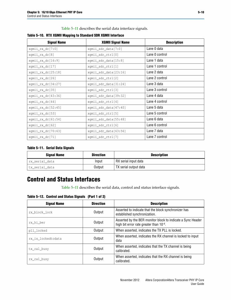
Chapter 5: 1G/10 Gbps Ethernet PHY IP Core 5–10Control and Status Interfaces
Table 5–11 describes the serial data interface signals.
Control and Status InterfacesTable 5–11 describes the serial data, control and status interface signals.
Table 5–10. RTX XGMII Mapping to Standard SDR XGMII Interface
Signal Name XGMII Signal Name Description
xgmii_rx_dc[7:0] xgmii_sdr_data[7:0] Lane 0 data
xgmii_rx_dc[8] xgmii_sdr_ctrl[0] Lane 0 control
xgmii_rx_dc[16:9] xgmii_sdr_data[15:8] Lane 1 data
xgmii_rx_dc[17] xgmii_sdr_ctrl[1] Lane 1 control
xgmii_rx_dc[25:18] xgmii_sdr_data[23:16] Lane 2 data
xgmii_rx_dc[26] xgmii_sdr_ctrl[2] Lane 2 control
xgmii_rx_dc[34:27] xgmii_sdr_data[31:24] Lane 3 data
xgmii_rx_dc[35] xgmii_sdr_ctrl[3] Lane 3 control
xgmii_rx_dc[43:36] xgmii_sdr_data[39:32] Lane 4 data
xgmii_rx_dc[44] xgmii_sdr_ctrl[4] Lane 4 control
xgmii_rx_dc[52:45] xgmii_sdr_data[47:40] Lane 5 data
xgmii_rx_dc[53] xgmii_sdr_ctrl[5] Lane 5 control
xgmii_rx_dc[61:54] xgmii_sdr_data[55:48] Lane 6 data
xgmii_rx_dc[62] xgmii_sdr_ctrl[6] Lane 6 control
xgmii_rx_dc[70:63] xgmii_sdr_data[63:56] Lane 7 data
xgmii_rx_dc[71] xgmii_sdr_ctrl[7] Lane 7 control
Table 5–11. Serial Data Signals
Signal Name Direction Description
rx_serial_data Input RX serial input data
tx_serial_data Output TX serial output data
Table 5–12. Control and Status Signals (Part 1 of 2)
Signal Name Direction Description
rx_block_lock Output Asserted to indicate that the block synchronizer has established synchronization.
rx_hi_ber Output Asserted by the BER monitor block to indicate a Sync Header high bit error rate greater than 10-4.
pll_locked Output When asserted, indicates the TX PLL is locked.
rx_is_lockedtodata Output When asserted, indicates the RX channel is locked to input data
tx_cal_busy Output When asserted, indicates that the TX channel is being calibrated.
rx_cal_busy Output When asserted, indicates that the RX channel is being calibrated.
November 2012 Altera CorporationAltera Transceiver PHY IP CoreUser Guide
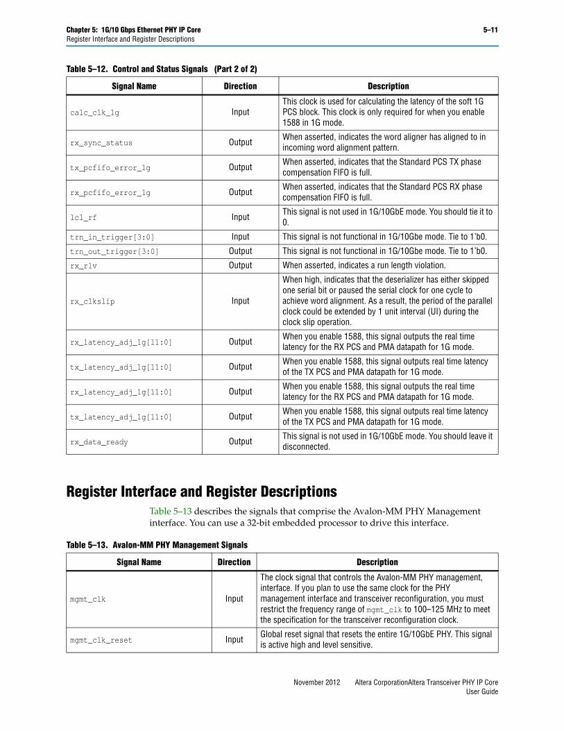
Chapter 5: 1G/10 Gbps Ethernet PHY IP Core 5–11Register Interface and Register Descriptions
Register Interface and Register DescriptionsTable 5–13 describes the signals that comprise the Avalon-MM PHY Management interface. You can use a 32-bit embedded processor to drive this interface.
calc_clk_1g InputThis clock is used for calculating the latency of the soft 1G PCS block. This clock is only required for when you enable 1588 in 1G mode.
rx_sync_status Output When asserted, indicates the word aligner has aligned to in incoming word alignment pattern.
tx_pcfifo_error_1g Output When asserted, indicates that the Standard PCS TX phase compensation FIFO is full.
rx_pcfifo_error_1g Output When asserted, indicates that the Standard PCS RX phase compensation FIFO is full.
lcl_rf Input This signal is not used in 1G/10GbE mode. You should tie it to 0.
trn_in_trigger[3:0] Input This signal is not functional in 1G/10Gbe mode. Tie to 1’b0.
trn_out_trigger[3:0] Output This signal is not functional in 1G/10Gbe mode. Tie to 1’b0.
rx_rlv Output When asserted, indicates a run length violation.
rx_clkslip Input
When high, indicates that the deserializer has either skipped one serial bit or paused the serial clock for one cycle to achieve word alignment. As a result, the period of the parallel clock could be extended by 1 unit interval (UI) during the clock slip operation.
rx_latency_adj_1g[11:0] Output When you enable 1588, this signal outputs the real time latency for the RX PCS and PMA datapath for 1G mode.
tx_latency_adj_1g[11:0] Output When you enable 1588, this signal outputs real time latency of the TX PCS and PMA datapath for 1G mode.
rx_latency_adj_1g[11:0] Output When you enable 1588, this signal outputs the real time latency for the RX PCS and PMA datapath for 1G mode.
tx_latency_adj_1g[11:0] Output When you enable 1588, this signal outputs real time latency of the TX PCS and PMA datapath for 1G mode.
rx_data_ready Output This signal is not used in 1G/10GbE mode. You should leave it disconnected.
Table 5–12. Control and Status Signals (Part 2 of 2)
Signal Name Direction Description
Table 5–13. Avalon-MM PHY Management Signals
Signal Name Direction Description
mgmt_clk Input
The clock signal that controls the Avalon-MM PHY management, interface. If you plan to use the same clock for the PHY management interface and transceiver reconfiguration, you must restrict the frequency range of mgmt_clk to 100–125 MHz to meet the specification for the transceiver reconfiguration clock.
mgmt_clk_reset Input Global reset signal that resets the entire 1G/10GbE PHY. This signal is active high and level sensitive.
November 2012 Altera CorporationAltera Transceiver PHY IP CoreUser Guide
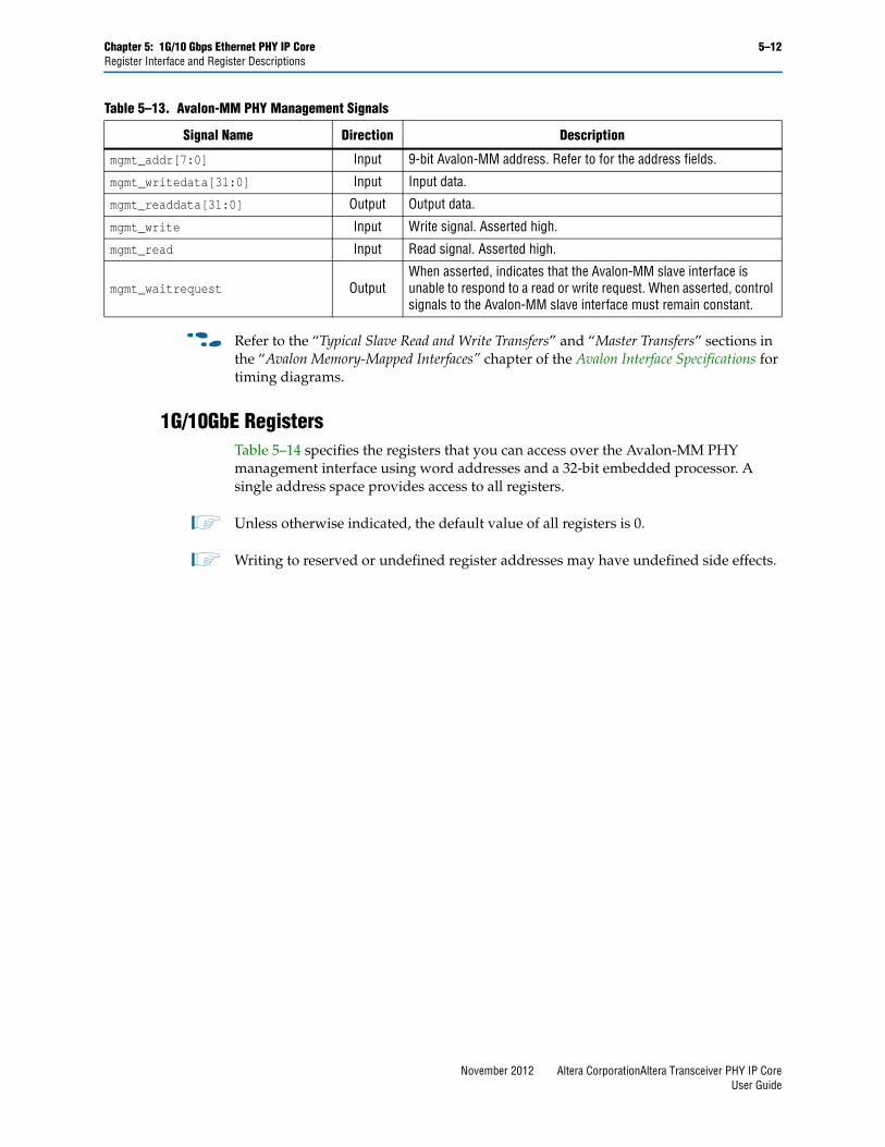
Chapter 5: 1G/10 Gbps Ethernet PHY IP Core 5–12Register Interface and Register Descriptions
f Refer to the “Typical Slave Read and Write Transfers” and “Master Transfers” sections in the “Avalon Memory-Mapped Interfaces” chapter of the Avalon Interface Specifications for timing diagrams.
1G/10GbE RegistersTable 5–14 specifies the registers that you can access over the Avalon-MM PHY management interface using word addresses and a 32-bit embedded processor. A single address space provides access to all registers.
1 Unless otherwise indicated, the default value of all registers is 0.
1 Writing to reserved or undefined register addresses may have undefined side effects.
mgmt_addr[7:0] Input 9-bit Avalon-MM address. Refer to for the address fields.
mgmt_writedata[31:0] Input Input data.
mgmt_readdata[31:0] Output Output data.
mgmt_write Input Write signal. Asserted high.
mgmt_read Input Read signal. Asserted high.
mgmt_waitrequest OutputWhen asserted, indicates that the Avalon-MM slave interface is unable to respond to a read or write request. When asserted, control signals to the Avalon-MM slave interface must remain constant.
Table 5–13. Avalon-MM PHY Management Signals
Signal Name Direction Description
November 2012 Altera CorporationAltera Transceiver PHY IP CoreUser Guide
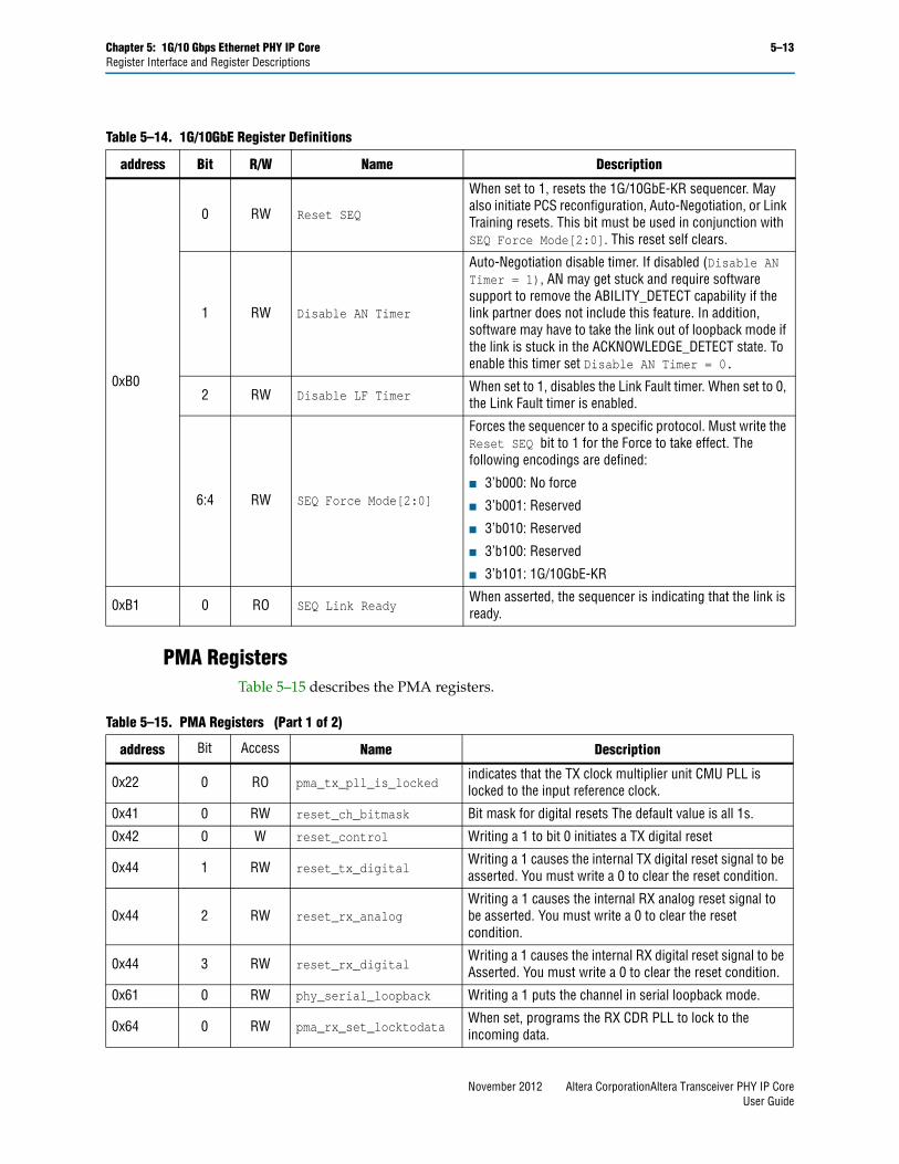
Chapter 5: 1G/10 Gbps Ethernet PHY IP Core 5–13Register Interface and Register Descriptions
PMA RegistersTable 5–15 describes the PMA registers.
Table 5–14. 1G/10GbE Register Definitions
address Bit R/W Name Description
0xB0
0 RW Reset SEQ
When set to 1, resets the 1G/10GbE-KR sequencer. May also initiate PCS reconfiguration, Auto-Negotiation, or Link Training resets. This bit must be used in conjunction with SEQ Force Mode[2:0]. This reset self clears.
1 RW Disable AN Timer
Auto-Negotiation disable timer. If disabled (Disable AN Timer = 1), AN may get stuck and require software support to remove the ABILITY_DETECT capability if the link partner does not include this feature. In addition, software may have to take the link out of loopback mode if the link is stuck in the ACKNOWLEDGE_DETECT state. To enable this timer set Disable AN Timer = 0.
2 RW Disable LF TimerWhen set to 1, disables the Link Fault timer. When set to 0, the Link Fault timer is enabled.
6:4 RW SEQ Force Mode[2:0]
Forces the sequencer to a specific protocol. Must write the Reset SEQ bit to 1 for the Force to take effect. The following encodings are defined:
■ 3’b000: No force
■ 3’b001: Reserved
■ 3’b010: Reserved
■ 3’b100: Reserved
■ 3’b101: 1G/10GbE-KR
0xB1 0 RO SEQ Link ReadyWhen asserted, the sequencer is indicating that the link is ready.
Table 5–15. PMA Registers (Part 1 of 2)
address Bit Access Name Description
0x22 0 RO pma_tx_pll_is_lockedindicates that the TX clock multiplier unit CMU PLL is locked to the input reference clock.
0x41 0 RW reset_ch_bitmask Bit mask for digital resets The default value is all 1s.
0x42 0 W reset_control Writing a 1 to bit 0 initiates a TX digital reset
0x44 1 RW reset_tx_digitalWriting a 1 causes the internal TX digital reset signal to be asserted. You must write a 0 to clear the reset condition.
0x44 2 RW reset_rx_analogWriting a 1 causes the internal RX analog reset signal to be asserted. You must write a 0 to clear the reset condition.
0x44 3 RW reset_rx_digitalWriting a 1 causes the internal RX digital reset signal to be Asserted. You must write a 0 to clear the reset condition.
0x61 0 RW phy_serial_loopback Writing a 1 puts the channel in serial loopback mode.
0x64 0 RW pma_rx_set_locktodataWhen set, programs the RX CDR PLL to lock to the incoming data.
November 2012 Altera CorporationAltera Transceiver PHY IP CoreUser Guide
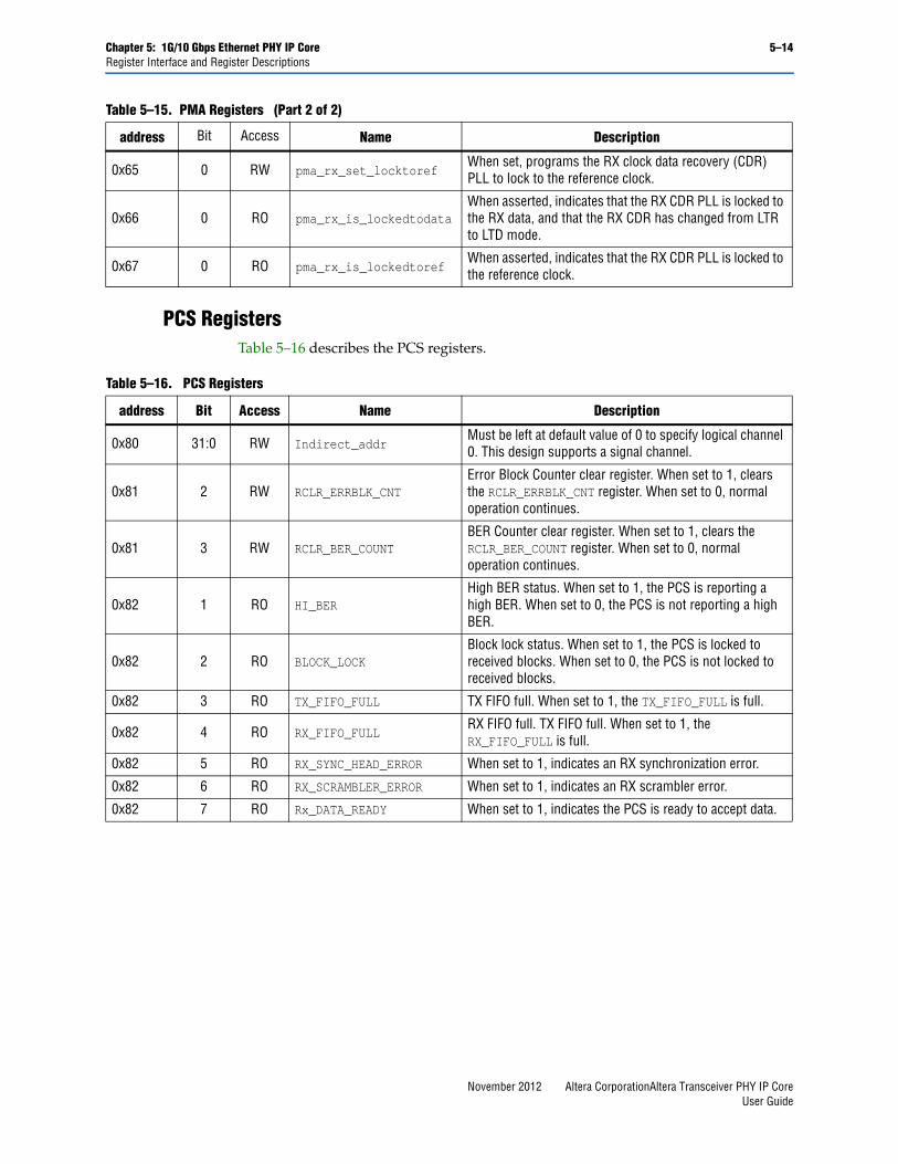
Chapter 5: 1G/10 Gbps Ethernet PHY IP Core 5–14Register Interface and Register Descriptions
PCS RegistersTable 5–16 describes the PCS registers.
0x65 0 RW pma_rx_set_locktorefWhen set, programs the RX clock data recovery (CDR) PLL to lock to the reference clock.
0x66 0 RO pma_rx_is_lockedtodataWhen asserted, indicates that the RX CDR PLL is locked to the RX data, and that the RX CDR has changed from LTR to LTD mode.
0x67 0 RO pma_rx_is_lockedtorefWhen asserted, indicates that the RX CDR PLL is locked to the reference clock.
Table 5–15. PMA Registers (Part 2 of 2)
address Bit Access Name Description
Table 5–16. PCS Registers
address Bit Access Name Description
0x80 31:0 RW Indirect_addrMust be left at default value of 0 to specify logical channel 0. This design supports a signal channel.
0x81 2 RW RCLR_ERRBLK_CNTError Block Counter clear register. When set to 1, clears the RCLR_ERRBLK_CNT register. When set to 0, normal operation continues.
0x81 3 RW RCLR_BER_COUNTBER Counter clear register. When set to 1, clears the RCLR_BER_COUNT register. When set to 0, normal operation continues.
0x82 1 RO HI_BERHigh BER status. When set to 1, the PCS is reporting a high BER. When set to 0, the PCS is not reporting a high BER.
0x82 2 RO BLOCK_LOCKBlock lock status. When set to 1, the PCS is locked to received blocks. When set to 0, the PCS is not locked to received blocks.
0x82 3 RO TX_FIFO_FULL TX FIFO full. When set to 1, the TX_FIFO_FULL is full.
0x82 4 RO RX_FIFO_FULLRX FIFO full. TX FIFO full. When set to 1, the RX_FIFO_FULL is full.
0x82 5 RO RX_SYNC_HEAD_ERROR When set to 1, indicates an RX synchronization error.
0x82 6 RO RX_SCRAMBLER_ERROR When set to 1, indicates an RX scrambler error.
0x82 7 RO Rx_DATA_READY When set to 1, indicates the PCS is ready to accept data.
November 2012 Altera CorporationAltera Transceiver PHY IP CoreUser Guide
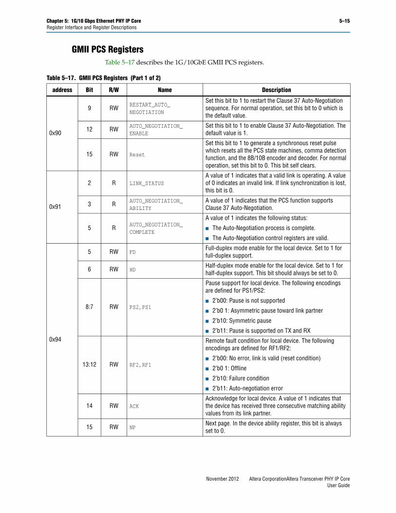
Chapter 5: 1G/10 Gbps Ethernet PHY IP Core 5–15Register Interface and Register Descriptions
GMII PCS RegistersTable 5–17 describes the 1G/10GbE GMII PCS registers.
Table 5–17. GMII PCS Registers (Part 1 of 2)
address Bit R/W Name Description
0x90
9 RW RESTART_AUTO_NEGOTIATION
Set this bit to 1 to restart the Clause 37 Auto-Negotiation sequence. For normal operation, set this bit to 0 which is the default value.
12 RW AUTO_NEGOTIATION_ENABLE
Set this bit to 1 to enable Clause 37 Auto-Negotiation. The default value is 1.
15 RW Reset
Set this bit to 1 to generate a synchronous reset pulse which resets all the PCS state machines, comma detection function, and the 8B/10B encoder and decoder. For normal operation, set this bit to 0. This bit self clears.
0x91
2 R LINK_STATUSA value of 1 indicates that a valid link is operating. A value of 0 indicates an invalid link. If link synchronization is lost, this bit is 0.
3 R AUTO_NEGOTIATION_ABILITY
A value of 1 indicates that the PCS function supports Clause 37 Auto-Negotiation.
5 R AUTO_NEGOTIATION_COMPLETE
A value of 1 indicates the following status:
■ The Auto-Negotiation process is complete.
■ The Auto-Negotiation control registers are valid.
0x94
5 RW FDFull-duplex mode enable for the local device. Set to 1 for full-duplex support.
6 RW HDHalf-duplex mode enable for the local device. Set to 1 for half-duplex support. This bit should always be set to 0.
8:7 RW PS2,PS1
Pause support for local device. The following encodings are defined for PS1/PS2:
■ 2’b00: Pause is not supported
■ 2’b0 1: Asymmetric pause toward link partner
■ 2’b10: Symmetric pause
■ 2’b11: Pause is supported on TX and RX
13:12 RW RF2,RF1
Remote fault condition for local device. The following encodings are defined for RF1/RF2:
■ 2’b00: No error, link is valid (reset condition)
■ 2’b0 1: Offline
■ 2’b10: Failure condition
■ 2’b11: Auto-negotiation error
14 RW ACKAcknowledge for local device. A value of 1 indicates that the device has received three consecutive matching ability values from its link partner.
15 RW NPNext page. In the device ability register, this bit is always set to 0.
November 2012 Altera CorporationAltera Transceiver PHY IP CoreUser Guide
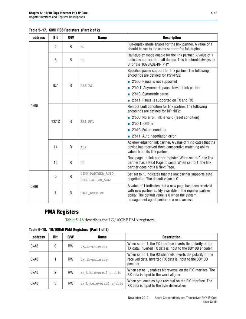
Chapter 5: 1G/10 Gbps Ethernet PHY IP Core 5–16Register Interface and Register Descriptions
PMA RegistersTable 5–18 describes the 1G/10GbE PMA registers.
0x95
5 R FDFull-duplex mode enable for the link partner. A value of 1 should be set to indicates support for full duplex.
6 R HDHalf-duplex mode enable for the link partner. A value of 1 indicates support for half duplex. This bit should always be 0 for the 10GBASE-KR PHY.
8:7 R PS2,PS1
Specifies pause support for link partner. The following encodings are defined for PS1/PS2:
■ 2’b00: Pause is not supported
■ 2’b0 1: Asymmetric pause toward link partner
■ 2’b10: Symmetric pause
■ 2’b11: Pause is supported on TX and RX
13:12 R RF2,RF1
Remote fault condition for link partner. The following encodings are defined for RF1/RF2:
■ 2’b00: No error, link is valid (reset condition)
■ 2’b0 1: Offline
■ 2’b10: Failure condition
■ 2’b11: Auto-negotiation error
14 R ACKAcknowledge for link partner. A value of 1 indicates that the device has received three consecutive matching ability values from its link partner.
15 R NPNext page. In link partner register. When set to 0, the link partner has a Next Page to send. When set to 1, the link partner does not a a Next Page.
0x96
0 RLINK_PARTNER_AUTO_
NEGOTIATION_ABLE
Set set to 1, indicates that the link partner supports auto negotiation. The default value is 0.
1 R PAGE_RECEIVE
A value of 1 indicates that a new page has been received with new partner ability available in the register partner ability. The default value is 0 when the system management agent performs a read access.
Table 5–17. GMII PCS Registers (Part 2 of 2)
address Bit R/W Name Description
Table 5–18. 1G/10GbE PMA Registers (Part 1 of 2)
address Bit R/W Name Description
0xA8 0 RW tx_invpolarityWhen set to 1, the TX interface inverts the polarity of the TX data. Inverted TX data is input to the 8B/10B encoder.
0xA8 1 RW rx_invpolarityWhen set to 1, the RX channels inverts the polarity of the received data. Inverted RX data is input to the 8B/10B decoder.
0xA8 2 RW rx_bitreversal_enableWhen set to 1, enables bit reversal on the RX interface. The RX data is input to the word aligner.
0xA8 3 RW rx_bytereversal_enableWhen set, enables byte reversal on the RX interface. The RX data is input to the byte deserializer.
November 2012 Altera CorporationAltera Transceiver PHY IP CoreUser Guide
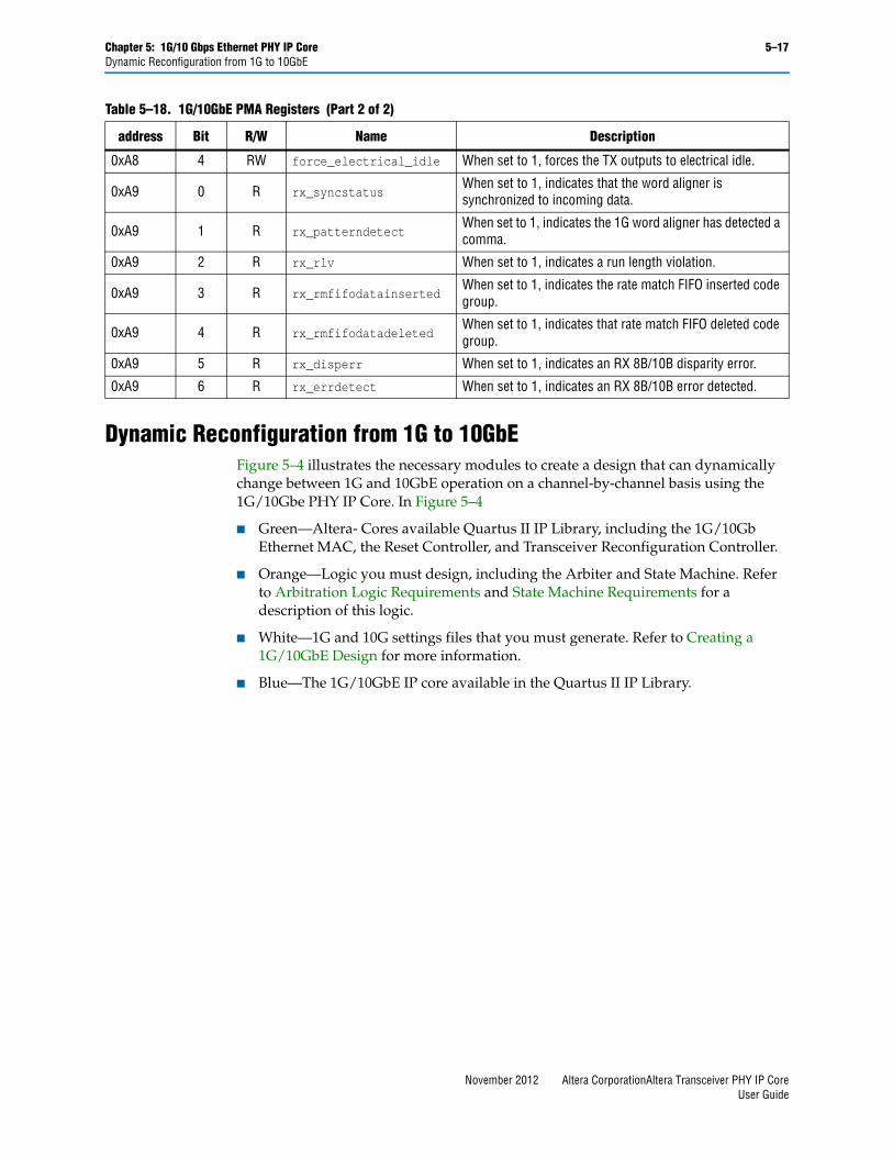
Chapter 5: 1G/10 Gbps Ethernet PHY IP Core 5–17Dynamic Reconfiguration from 1G to 10GbE
Dynamic Reconfiguration from 1G to 10GbEFigure 5–4 illustrates the necessary modules to create a design that can dynamically change between 1G and 10GbE operation on a channel-by-channel basis using the 1G/10Gbe PHY IP Core. In Figure 5–4
■ Green—Altera- Cores available Quartus II IP Library, including the 1G/10Gb Ethernet MAC, the Reset Controller, and Transceiver Reconfiguration Controller.
■ Orange—Logic you must design, including the Arbiter and State Machine. Refer to Arbitration Logic Requirements and State Machine Requirements for a description of this logic.
■ White—1G and 10G settings files that you must generate. Refer to Creating a 1G/10GbE Design for more information.
■ Blue—The 1G/10GbE IP core available in the Quartus II IP Library.
0xA8 4 RW force_electrical_idle When set to 1, forces the TX outputs to electrical idle.
0xA9 0 R rx_syncstatusWhen set to 1, indicates that the word aligner is synchronized to incoming data.
0xA9 1 R rx_patterndetectWhen set to 1, indicates the 1G word aligner has detected a comma.
0xA9 2 R rx_rlv When set to 1, indicates a run length violation.
0xA9 3 R rx_rmfifodatainsertedWhen set to 1, indicates the rate match FIFO inserted code group.
0xA9 4 R rx_rmfifodatadeletedWhen set to 1, indicates that rate match FIFO deleted code group.
0xA9 5 R rx_disperr When set to 1, indicates an RX 8B/10B disparity error.
0xA9 6 R rx_errdetect When set to 1, indicates an RX 8B/10B error detected.
Table 5–18. 1G/10GbE PMA Registers (Part 2 of 2)
address Bit R/W Name Description
November 2012 Altera CorporationAltera Transceiver PHY IP CoreUser Guide
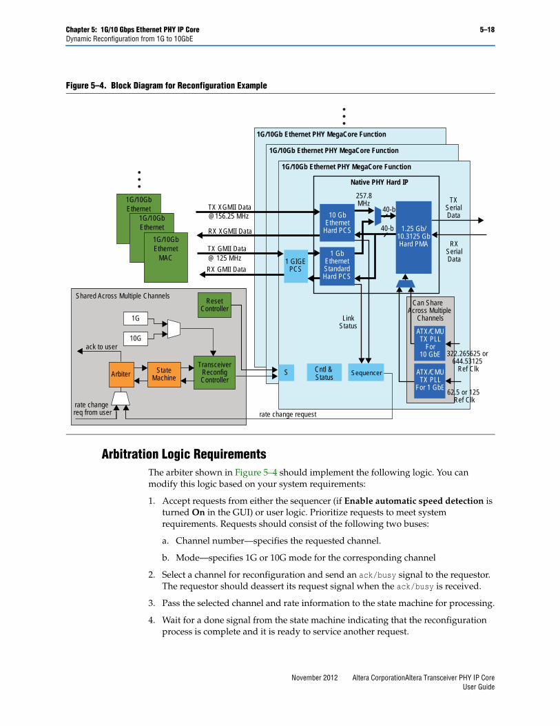
Chapter 5: 1G/10 Gbps Ethernet PHY IP Core 5–18Dynamic Reconfiguration from 1G to 10GbE
Arbitration Logic RequirementsThe arbiter shown in Figure 5–4 should implement the following logic. You can modify this logic based on your system requirements:
1. Accept requests from either the sequencer (if Enable automatic speed detection is turned On in the GUI) or user logic. Prioritize requests to meet system requirements. Requests should consist of the following two buses:
a. Channel number—specifies the requested channel.
b. Mode—specifies 1G or 10G mode for the corresponding channel
2. Select a channel for reconfiguration and send an ack/busy signal to the requestor. The requestor should deassert its request signal when the ack/busy is received.
3. Pass the selected channel and rate information to the state machine for processing.
4. Wait for a done signal from the state machine indicating that the reconfiguration process is complete and it is ready to service another request.
Figure 5–4. Block Diagram for Reconfiguration Example
1G/10GbEthernet
MAC
1G/10Gb Ethernet PHY MegaCore Function
1G/10Gb Ethernet PHY MegaCore Function
1G/10Gb Ethernet PHY MegaCore Function
Native PHY Hard IP
257.8MHz
40-b
40-bTX
SerialData
RXSerialData
322.265625 or 644.53125
Ref Clk
62.5 or 125 Ref Clk
ATX/CMUTX PLL
For10 GbE
ATX/CMUTX PLL
For 1 GbE
1.25 Gb/10.3125 GbHard PMA
LinkStatus
SequencerS
ResetController
StateMachineArbiter
rate change request
ack to user
rate change req from user
TransceiverReconfigController
10 GbEthernet
Hard PCS
Cntl & Status
RX GMII Data
TX GMII Data@ 125 MHz
RX XGMII Data
TX XGMII Data
Shared Across Multiple ChannelsCan Share
Across Multiple Channels
@156.25 MHz
1 GIGEPCS
1G/10GbEthernet
MAC1G/10GbEthernet
MAC
1G
10G
1 GbEthernetStandardHard PCS
November 2012 Altera CorporationAltera Transceiver PHY IP CoreUser Guide
Chapter 5: 1G/10 Gbps Ethernet PHY IP Core 5–19Creating a 1G/10GbE Design
State Machine RequirementsThe state machine shown in Figure 5–4 should implement the following logic. You can modify this logic based on your system requirements:
1. Wait for reconfig_busy from the Transceiver Reconfiguration Controller to be deasserted and the tx_ready and rx_ready signals from the Transceiver PHY Reset Controller to be asserted. These conditions indicate that the system is ready to service a reconfiguration request.
2. Set the appropriate channel for reconfiguration.
3. Initiate the MIF streaming process. The state machine should also select the appropriate MIF (stored in the ROMs) to stream based on the requested mode. For more information about MIF mode, refer to the Streamer Module Registers.
4. Wait for the reconfig_busy signal from the Transceiver Reconfiguration Controller to assert and then deassert indicating the reconfiguration process is complete.
5. Toggle the digital resets for the reconfigured channel and wait for the link to be ready.
6. Deassert the ack/busy signal for the selected channel. Deassertion of ack/busy indicates to the arbiter that the reconfiguration process is complete and the system is ready to service another request.
Creating a 1G/10GbE DesignComplete the following steps to create a 10GBASE-KR design using this PHY.
1. Generate the 1G/10GbE PHY with the required parameterization.
2. Generate a Transceiver Reconfiguration Controller with the correct number of reconfiguration interfaces based on the number of channels you are using. This controller is connected to all the transceiver channels. It implements the reconfiguration process.
3. Generate a Transceiver Reset Controller.
4. Create arbitration logic that prioritizes simultaneous reconfiguration requests from multiple channels. This logic should also acknowledge the channel being serviced causing the requestor to deassert its request signal.
5. Create a state machine that controls the reconfiguration process. The state machine should:
a. Receive the prioritized reconfiguration request from the arbiter.
b. Put the Transceiver Reconfiguration Controller into MIF streaming mode.
c. Select the correct MIF and stream it into the appropriate channel.
d. Wait for the reconfiguration process to end and provide status signal to arbiter.
6. Generate one ROM for each required configuration.
7. Create a MIF for each configuration and associate each MIF with a ROM created in Step 6. For example, create a MIF for 1G with 1588 and a MIF for 10G with 1588. These MIFs are the two configurations used in the MIF streaming process. For more information on creating MIFs, refer to MIF Generation.
November 2012 Altera CorporationAltera Transceiver PHY IP CoreUser Guide
Chapter 5: 1G/10 Gbps Ethernet PHY IP Core 5–20Editing a MIF File
8. Generate a fractional PLL to create the 156.25 MHz XGMII clock from the 10G reference clock.
9. Instantiate the PHY in your design to determine the required number of channels.
10. To complete the system, connect all the blocks.
Editing a MIF FileThe MIF format contains all bit settings for the transceiver PMA and PCS. Because the 1G/10GbE PHY IP Core only requires PCS reconfiguration for a rate change, the PMA settings should not change. Removing the PMA settings from the MIF file also prevents an unintended overwrite of PMA parameters set through other assignments. A few simple edits to the MIF file removes the PMA settings.
Complete the following steps to edit the MIF file:
1. Replace line 17 with “13: 0001000000010110; -- PMA - RX changed to removed CTLE”.
2. Replace line 20 with “16: 0010100000011001; -- PMA - RX continued”.
3. Replace line 4 with “4: 0001000000000000; -- PMA - TX”.
4. Remove lines 7-10. These lines contain the TX settings (VOD, post-tap, pre-tap).
5. Renumber the lines starting with the old line 11.
6. Change the depth at the top of the file from 168 to 164.
November 2012 Altera CorporationAltera Transceiver PHY IP CoreUser Guide
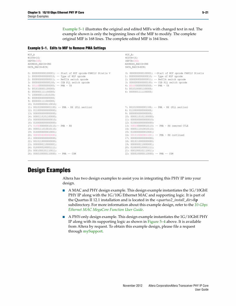
Chapter 5: 1G/10 Gbps Ethernet PHY IP Core 5–21Design Examples
Example 5–1 illustrates the original and edited MIFs with changed text in red. The example shown is only the beginning lines of the MIF to modify. The complete original MIF is 168 lines. The complete edited MIF is 164 lines.
Design ExamplesAltera has two design examples to assist you in integrating this PHY IP into your design.
■ A MAC and PHY design example. This design example instantiates the 1G/10GbE PHY IP along with the 1G/10G Ethernet MAC and supporting logic. It is part of the Quartus II 12.1 installation and is located in the <quartus2_install_dir>/ip subdirectory. For more information about this example design, refer to the 10-Gbps Ethernet MAC MegaCore Function User Guide.
■ A PHY-only design example. This design example instantiates the 1G/10GbE PHY IP along with its supporting logic as shown in Figure 5–4 above. It is available from Altera by request. To obtain this example design, please file a request through mySupport.
Example 5–1. Edits to MIF to Remove PMA Settings
MIF_A MIF_B;WIDTH=16; WIDTH=16;DEPTH=168; DEPTH=164;ADDRESS_RADIX=UNS ADDRESS_RADIX=UNSDATA_RADIX=BIN; DATA_RADIX=BIN;
0: 0000000000100001; -- Start of MIF opcode-FAMILY Stratix V 0: 0000000000100001; --Start of MIF opcode FAMILY Stratix 1: 0000000000000010; -- Type of MIF opcode 1: 0000000000000010; -- Type of MIF opcode2: 0000000000000011; -- RefClk switch opcode 2: 0000000000000011; -- RefClk switch opcode3: 0000000000000100; -- CGB PLL switch opcode 3: 0000000000000100; -- CGB PLL switch opcode4: 0011000000000000; -- PMA - TX 4: 0010000000000000; -- PMA - TX5: 0010100001100000; 5: 0010100001100000;6: 0000001111100000; 6: 0000001111100000;7: 1000000111010100;8: 0000000000000000;9: 0000001111000000;10: 0100000000110010;11: 0010100000001100; -- PMA - RX (PLL section) 7: 0010100000001100; -- PMA - RX (PLL section)12: 0110000000000000; 8: 0110000000000000; 13: 0000000000000000; 9: 0000000000000000;14: 0000110101100000; 10: 0000110101100000;15: 0000000000000010; 11: 0000000000000010;16: 0100000000000000; 12: 0100000000000000;17: 0100000000010110;-- PMA - RX 13: 0001000000010110; -- PMA - RX removed CTLE18: 0000111010010110; 14: 0000111010010110; 19: 0100000000010001; 15: 0100000000010001;20: 0000000000000000; 16: 0010100000011001; -- PMA - RX continued21: 0000000000000000; 17: 0000000000000000;22: 0010110000000000; 18: 0010110000000000;23: 0000000110000001; 19: 0000000110000001;24: 0100000100001111; 20: 0100000100001111; 25: 0001000101110011; 21: 0001000101110011;26: 0000100000110000; -- PMA -- COM 22: 0000100000110000; -- PMA -- COM
November 2012 Altera CorporationAltera Transceiver PHY IP CoreUser Guide
Chapter 5: 1G/10 Gbps Ethernet PHY IP Core 5–22Dynamic Reconfiguration
Dynamic ReconfigurationTable 5–19 describes the signals the dynamic reconfiguration interface.
Table 5–19. Dynamic Reconfiguration Signals
Signal Name Direction Description
reconfig_to_xcvr[(<n>70-1):0]
InputReconfiguration signals from the Reconfiguration Design Example. <n> grows linearly with the number of reconfiguration interfaces.
reconfig_from_xcvr[(<n>46-1):0]
OutputReconfiguration signals to the Reconfiguration Design Example. <n> grows linearly with the number of reconfiguration interfaces.
rc_busy Input When asserted, indicates that reconfig is in progress.
lt_start_rc Output When asserted, starts the TX PMA equalization reconfiguration.
main_rc[5:0] Output The main TX equalization tap value which is the same as VOD.
post_rc[4:0] Output The post-cursor TX equalization tap value.
pre_rc[3:0] Output The pre-cursor TX equalization tap value.
tap_to_upd[2:0] Output
Specifies the TX equalization tap to update to optimize signal quality. The following encodings are defined:
■ 3’b100: main tap
■ 3’b010: post-tap
■ 3’b001: pre-tap
seq_start_rc Output When asserted, starts PCS reconfiguration.
pcs_mode_rc[5:0] Output
Specifies the PCS mode for reconfig using 1-hot encoding. The following modes are defined in 1G/10GbE mode:
■ 6’b000001: Reserved
■ 6’b000010: Reserved
■ 6’b000100: 10G data mode
■ 6’b001000: 1G data mode
■ 6’b010000: Reserved
■ 6’b100000: Reserved
mode_1g_10gbar Input This signal indicates the requested mode for the channel. A 1 indicates 1G mode and a 0 indicates 10G mode.
en_lcl_rxeq Output Not functional in 1G/10GbE mode. Leave disconnected.
rxeq_done Input Not functional in 1G/10GbE mode. Set to 1’b1.
November 2012 Altera CorporationAltera Transceiver PHY IP CoreUser Guide
Chapter 5: 1G/10 Gbps Ethernet PHY IP Core 5–23Simulation
SimulationThe 1G/10GbE PHY IP Core support ModelSim Verilog and ModelSim VHDL, VCS Verilog, and VCS VHDL simulation. Stratix V devices also support NCSIM Verilog and MCSIM VHDL simulation. The MegaWizard Plug-In Manager generates an IP functional simulation model when you press the Finish button.
TimeQuest Timing ConstraintsTo pass timing analysis, you must decouple the clocks in different time domains. The necessary Synopsys Design Constraints File (.sdc) timing constraints for the 1G/10GbE IP Core are included in the top-level wrapper file.
AcronymsTable 5–20 lists commonly used acronyms for the 1G/10GbE PHY IP Core.
Table 5–20. Common Ethernet Acronyms
Acronym Definition
AN Auto-Negotiation in Ethernet as described in Clause 73 or of IEEE 802.3ap-2007.
BER Bit Error Rate.
DME Differential Manchester Encoding.
FEC Forward error correction.
GMII Gigabit Media Independent Interface.
KR Short hand notation for Backplane Ethernet with 64b/66b encoding.
LD Local Device.
LT Link training in backplane Ethernet Clause 72 for 10GBASE-KR and 40GBASE-KR4.
LP Link partner, to which the LD is connected.
MAC Media Access Control.
MII Media independent interface.
OSI Open System Interconnection.
PCS Physical Coding Sublayer.
PHY Physical Layer in OSI 7-layer architecture, also in Altera device scope is: PCS + PMA.
PMA Physical Medium Attachment.
PMD Physical Medium Dependent.
SGMII Serial Gigabit Media Independent Interface.
WAN Wide Area Network.
XAUI 10 Gigabit Attachment Unit Interface.
November 2012 Altera CorporationAltera Transceiver PHY IP CoreUser Guide

5–24 Chapter 5: 1G/10 Gbps Ethernet PHY IP CoreAcronyms
Altera Transceiver PHY IP Core November 2012 Altera CorporationUser Guide
November 2012 Altera Corporation
6. XAUI PHY IP Core
The Altera XAUI PHY IP Core implements the IEEE 802.3 Clause 48 specification to extend the operational distance of the XGMII interface and reduce the number of interface signals. XAUI extends the physical separation possible between the 10 Gbps Ethernet MAC function and the Ethernet standard PHY component to one meter. The XAUI IP Core accepts 72-bit data (single data rate–SDR XGMII) from the application layer at either 156.25 Mbps or 312.5 Mbps. The serial interface runs at either 4 × 3.125 Gbps or 4 × 6.25 Gbps (DDR XAUI option).
Figure 6–1 illustrates the top-level blocks of the XAUI PHY IP Core.
For Stratix IV GX and GT devices, you can choose a hard XAUI physical coding sublayer (PCS) and physical media attachment (PMA), or a soft XAUI PCS and PMA in low latency mode. You can also combine both hard and soft PCS configurations in the same device, using all channels in a transceiver bank. The PCS is only available in soft logic for Stratix V devices.
f For more detailed information about the XAUI transceiver channel datapath, clocking, and channel placement, refer to the “XAUI” section in the Transceiver Configurations in Stratix V Devices chapter of the Stratix V Device Handbook.
Figure 6–1. XAUI PHY IP Core
XAUI IP Core
4 x 3.125 Gbps serialor
4 x 6.5 Gbps serial
Altera FPGA
Hard PMA
PCS
8B/10BWord AlignerPhase Comp
SDR XGMII72 bits @ 156.25 Mbps
or72 bits @ 312.5 Mbps
Avalon-MMControl & Status
4
4
Altera Transceiver PHY IP CoreUser Guide
6–2 Chapter 6: XAUI PHY IP CoreRelease Information
Release InformationTable 6–1 provides information about this release of the XAUI PHY IP Core.
Device Family SupportIP cores provide either final or preliminary support for target Altera device families. These terms have the following definitions:
■ Final support—Verified with final timing models for this device.
■ Preliminary support—Verified with preliminary timing models for this device.
Table 6–2 shows the level of support offered by the XAUI IP Core for Altera device families.
Table 6–1. XAUI Release Information
Item Description
Version 12.0
Release Date November 2012
Ordering Codes (1) IP-XAUIPCS (primary)–Soft PCSIPR-XAUIPCS (renewal)–Soft PCS
Product ID 00D7
Vendor ID 6AF7
Note to Table 6–1:
(1) No ordering codes or license files are required for the hard PCS and PMA PHY in Arria II GX, Cyclone® IV GX, or Stratix IV GX or GT devices.
Table 6–2. Device Family Support
Device Family Support
XAUI
Arria II GX –Hard PCS and PMA Final
Arria II GZ–Hard PCS and PMA Final
Arria V GX–Soft PCS + PMA Preliminary
Arria V SoC–Soft PCS + PMA Preliminary
Arria V GZ devices–Soft PCS + PMA Preliminary
Cyclone IV GX–Hard PCS and PMA Final
Cyclone V–Soft PCS + PMA Preliminary
Cyclone V SoC–Soft PCS + hard PMA Preliminary
HardCopy® IV Final
Stratix IV GX and GT devices–Soft or hard PCS and PMA Final
Stratix V devices–Soft PCS + PMA Preliminary
Other device families No support
DXAUI
Stratix IV GX and GT Final
Other device families No support
Altera Transceiver PHY IP Core November 2012 Altera CorporationUser Guide
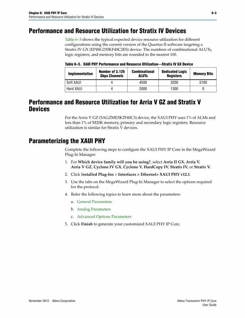
Chapter 6: XAUI PHY IP Core 6–3Performance and Resource Utilization for Stratix IV Devices
Performance and Resource Utilization for Stratix IV DevicesTable 6–3 shows the typical expected device resource utilization for different configurations using the current version of the Quartus II software targeting a Stratix IV GX (EP4SG230KF40C2ES) device. The numbers of combinational ALUTs, logic registers, and memory bits are rounded to the nearest 100.
Performance and Resource Utilization for Arria V GZ and Stratix V Devices
For the Arria V GZ (5AGZME5K2F40C3) device, the XAUI PHY uses 1% of ALMs and less than 1% of M20K memory, primary and secondary logic registers. Resource utilization is similar for Stratix V devices.
Parameterizing the XAUI PHY Complete the following steps to configure the XAUI PHY IP Core in the MegaWizard Plug-In Manager:
1. For Which device family will you be using?, select Arria II GX, Arria V, Arria V GZ, Cyclone IV GX, Cyclone V, HardCopy IV, Stratix IV, or Stratix V.
2. Click Installed Plug-Ins > Interfaces > Ethernet> XAUI PHY v12.1.
3. Use the tabs on the MegaWizard Plug-In Manager to select the options required for the protocol.
4. Refer the following topics to learn more about the parameters:
a. General Parameters
b. Analog Parameters
c. Advanced Options Parameters
5. Click Finish to generate your customized XAUI PHY IP Core.
Table 6–3. XAUI PHY Performance and Resource Utilization—Stratix IV GX Device
Implementation Number of 3.125 Gbps Channels
Combinational ALUTs
Dedicated Logic Registers Memory Bits
Soft XAUI 4 4500 3200 5100
Hard XAUI 4 2000 1300 0
November 2012 Altera Corporation Altera Transceiver PHY IP CoreUser Guide
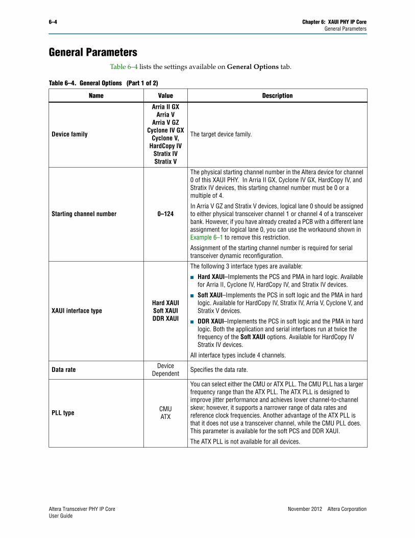
6–4 Chapter 6: XAUI PHY IP CoreGeneral Parameters
General ParametersTable 6–4 lists the settings available on General Options tab.
Table 6–4. General Options (Part 1 of 2)
Name Value Description
Device family
Arria II GXArria V
Arria V GZCyclone IV GX
Cyclone V,HardCopy IV
Stratix IVStratix V
The target device family.
Starting channel number 0–124
The physical starting channel number in the Altera device for channel 0 of this XAUI PHY. In Arria II GX, Cyclone IV GX, HardCopy IV, and Stratix IV devices, this starting channel number must be 0 or a multiple of 4.
In Arria V GZ and Stratix V devices, logical lane 0 should be assigned to either physical transceiver channel 1 or channel 4 of a transceiver bank. However, if you have already created a PCB with a different lane assignment for logical lane 0, you can use the workaound shown in Example 6–1 to remove this restriction.
Assignment of the starting channel number is required for serial transceiver dynamic reconfiguration.
XAUI interface typeHard XAUISoft XAUIDDR XAUI
The following 3 interface types are available:
■ Hard XAUI–Implements the PCS and PMA in hard logic. Available for Arria II, Cyclone IV, HardCopy IV, and Stratix IV devices.
■ Soft XAUI–Implements the PCS in soft logic and the PMA in hard logic. Available for HardCopy IV, Stratix IV, Arria V, Cyclone V, and Stratix V devices.
■ DDR XAUI–Implements the PCS in soft logic and the PMA in hard logic. Both the application and serial interfaces run at twice the frequency of the Soft XAUI options. Available for HardCopy IV Stratix IV devices.
All interface types include 4 channels.
Data rate Device Dependent Specifies the data rate.
PLL type CMUATX
You can select either the CMU or ATX PLL. The CMU PLL has a larger frequency range than the ATX PLL. The ATX PLL is designed to improve jitter performance and achieves lower channel-to-channel skew; however, it supports a narrower range of data rates and reference clock frequencies. Another advantage of the ATX PLL is that it does not use a transceiver channel, while the CMU PLL does. This parameter is available for the soft PCS and DDR XAUI.
The ATX PLL is not available for all devices.
Altera Transceiver PHY IP Core November 2012 Altera CorporationUser Guide
Chapter 6: XAUI PHY IP Core 6–5Analog Parameters
Example 6–1 shows how to remove the restriction on logical lane 0 channel assignment in Stratix V devices by redefining the pma_bonding_master parameter using the Quartus II Assignment Editor. In this example, the pma_bonding_master was originally assigned to physical channel 1. (The original assignment could also have been to physical channel 4.) The to parameter reassigns the pma_bonding_master to the XAUI instance name shown in quotation marks. You must substitute the instance name from your design for the instance name shown in quotation marks
Analog ParametersClick on the appropriate link to specify the analog options for your device:
■ Analog Parameters for Arria II GX, Cyclone IV GX, HardCopy IV and Stratix IV Devices
■ Analog Settings for Arria V Devices
■ Analog Settings for Arria V GZ Devices
■ Analog Settings for Cyclone V Devices
■ Analog Settings for Stratix V Devices
Base data rate1 × Lane rate2 × Lane rate4 × Lane rate
The base data rate is the frequency of the clock input to the PLL. Select a base data rate that minimizes the number of PLLs required to generate all the clock s required for data transmission. By selecting an appropriate base data rate, you can change data rates by changing the divider used by the clock generation block. This parameter is available for Stratix V devices.
Number of XAUI interfaces 1 Specifies the number of XAUI interfaces. Only 1 is available in the current release.
Table 6–4. General Options (Part 2 of 2)
Name Value Description
Example 6–1. Overriding Logical Lane 0 Channel Assignment Restrictions in Stratix V Devices
set_parameter -name pma_bonding_master "\"1\"" -to "<xaui instance name>|sv_xcvr_xaui:alt_xaui_phy|sv_xcvr_low_latency_phy_nr:alt_pma_0|sv_xcvr_custom_native:sv_xcvr_custom_inst|sv_xcvr_native:gen.sv_xcvr_native_insts[0].gen_bonded_group.sv_xcvr_native_inst"
November 2012 Altera Corporation Altera Transceiver PHY IP CoreUser Guide
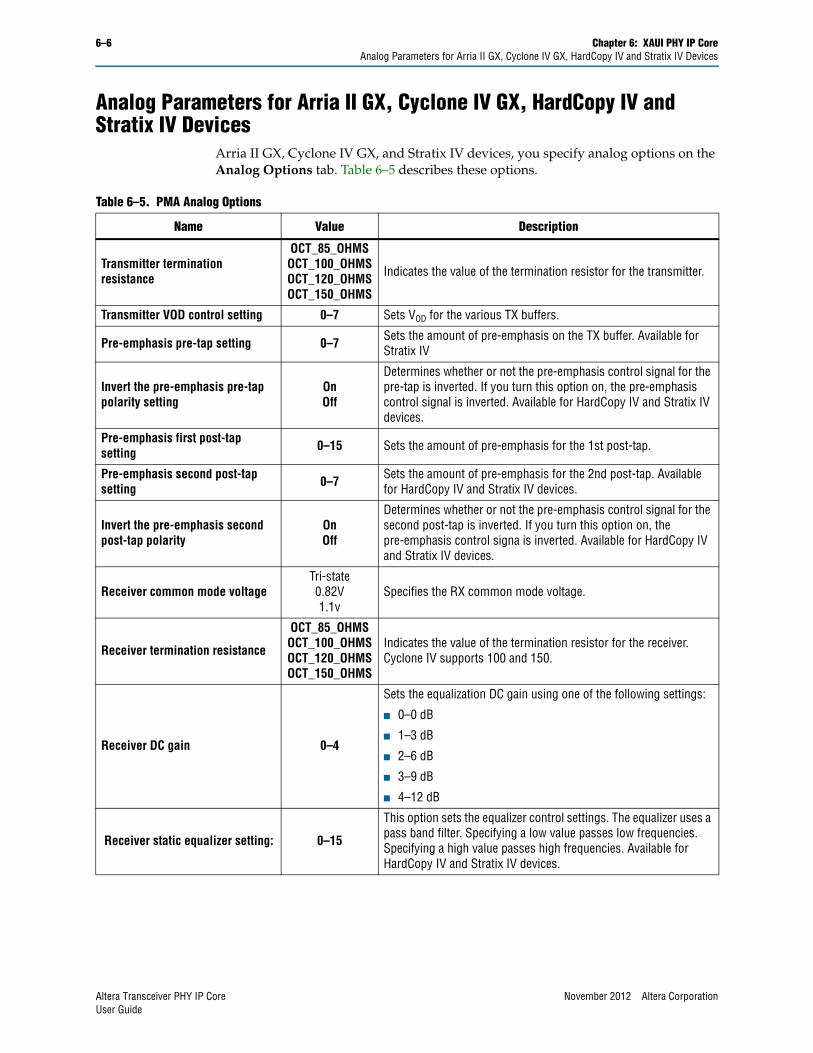
6–6 Chapter 6: XAUI PHY IP CoreAnalog Parameters for Arria II GX, Cyclone IV GX, HardCopy IV and Stratix IV Devices
Analog Parameters for Arria II GX, Cyclone IV GX, HardCopy IV and Stratix IV Devices
Arria II GX, Cyclone IV GX, and Stratix IV devices, you specify analog options on the Analog Options tab. Table 6–5 describes these options.
Table 6–5. PMA Analog Options
Name Value Description
Transmitter termination resistance
OCT_85_OHMS OCT_100_OHMS OCT_120_OHMS OCT_150_OHMS
Indicates the value of the termination resistor for the transmitter.
Transmitter VOD control setting 0–7 Sets VOD for the various TX buffers.
Pre-emphasis pre-tap setting 0–7 Sets the amount of pre-emphasis on the TX buffer. Available for Stratix IV
Invert the pre-emphasis pre-tap polarity setting
On Off
Determines whether or not the pre-emphasis control signal for the pre-tap is inverted. If you turn this option on, the pre-emphasis control signal is inverted. Available for HardCopy IV and Stratix IV devices.
Pre-emphasis first post-tap setting 0–15 Sets the amount of pre-emphasis for the 1st post-tap.
Pre-emphasis second post-tap setting 0–7 Sets the amount of pre-emphasis for the 2nd post-tap. Available
for HardCopy IV and Stratix IV devices.
Invert the pre-emphasis second post-tap polarity
On Off
Determines whether or not the pre-emphasis control signal for the second post-tap is inverted. If you turn this option on, the pre-emphasis control signa is inverted. Available for HardCopy IV and Stratix IV devices.
Receiver common mode voltageTri-state0.82V1.1v
Specifies the RX common mode voltage.
Receiver termination resistance
OCT_85_OHMS OCT_100_OHMS OCT_120_OHMS OCT_150_OHMS
Indicates the value of the termination resistor for the receiver. Cyclone IV supports 100 and 150.
Receiver DC gain 0–4
Sets the equalization DC gain using one of the following settings:
■ 0–0 dB
■ 1–3 dB
■ 2–6 dB
■ 3–9 dB
■ 4–12 dB
Receiver static equalizer setting: 0–15
This option sets the equalizer control settings. The equalizer uses a pass band filter. Specifying a low value passes low frequencies. Specifying a high value passes high frequencies. Available for HardCopy IV and Stratix IV devices.
Altera Transceiver PHY IP Core November 2012 Altera CorporationUser Guide
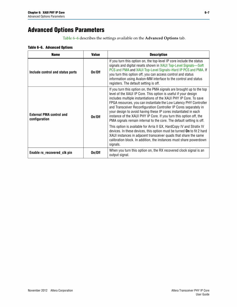
Chapter 6: XAUI PHY IP Core 6–7Advanced Options Parameters
Advanced Options ParametersTable 6–6 describes the settings available on the Advanced Options tab.
Table 6–6. Advanced Options
Name Value Description
Include control and status ports On/Off
If you turn this option on, the top-level IP core include the status signals and digital resets shown in XAUI Top-Level Signals—Soft PCS and PMA and XAUI Top-Level Signals–Hard IP PCS and PMA. If you turn this option off, you can access control and status information using Avalon-MM interface to the control and status registers. The default setting is off.
External PMA control and configuration On/Off
If you turn this option on, the PMA signals are brought up to the top level of the XAUI IP Core. This option is useful if your design includes multiple instantiations of the XAUI PHY IP Core. To save FPGA resources, you can instantiate the Low Latency PHY Controller and Transceiver Reconfiguration Controller IP Cores separately in your design to avoid having these IP cores instantiated in each instance of the XAUI PHY IP Core. If you turn this option off, the PMA signals remain internal to the core. The default setting is off.
This option is available for Arria II GX, HardCopy IV and Stratix IV devices. In these devices, this option must be turned On to fit 2 hard XAUI instances in adjacent transceiver quads that share the same calibration block. In addition, the instances must share powerdown signals.
Enable rx_recovered_clk pin On/Off When you turn this option on, the RX recovered clock signal is an output signal.
November 2012 Altera Corporation Altera Transceiver PHY IP CoreUser Guide
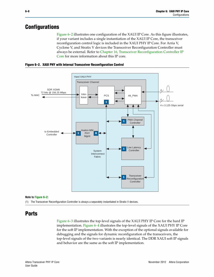
6–8 Chapter 6: XAUI PHY IP CoreConfigurations
ConfigurationsFigure 6–2 illustrates one configuration of the XAUI IP Core. As this figure illustrates, if your variant includes a single instantiation of the XAUI IP Core, the transceiver reconfiguration control logic is included in the XAUI PHY IP Core. For Arria V, Cyclone V, and Stratix V devices the Transceiver Reconfiguration Controller must always be external. Refer to Chapter 16, Transceiver Reconfiguration Controller IP Core for more information about this IP core.
PortsFigure 6–3 illustrates the top-level signals of the XAUI PHY IP Core for the hard IP implementation. Figure 6–4 illustrates the top-level signals of the XAUI PHY IP Core for the soft IP implementation. With the exception of the optional signals available for debugging and the signals for dynamic reconfiguration of the transceivers, the top-level signals of the two variants is nearly identical. The DDR XAUI soft IP signals and behavior are the same as the soft IP implementation.
Figure 6–2. XAUI PHY with Internal Transceiver Reconfiguration Control
Note to Figure 6–2:
(1) The Transceiver Reconfiguration Controller is always a separately instantiated in Stratix V devices.
System Interconnect
Fabric
Inter-leave
PCS
S
Alt_PMA
S
S Low LatencyController
S TransceiverReconfiguration
Controller
Transceiver Channel
Hard XAUI PHY
4 x 3.125 Gbps serial
to EmbeddedController
4
4
To MAC
SDR XGMII72 bits @ 156.25 Mbps
MAvalon-MM
PHYMgmt
S
PMA ChannelController
Altera Transceiver PHY IP Core November 2012 Altera CorporationUser Guide
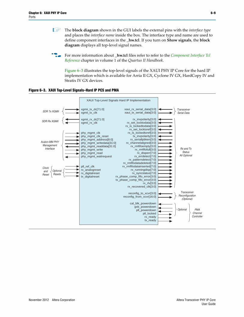
Chapter 6: XAUI PHY IP Core 6–9Ports
1 The block diagram shown in the GUI labels the external pins with the interface type and places the interface name inside the box. The interface type and name are used to define component interfaces in the _hw.tcl. If you turn on Show signals, the block diagram displays all top-level signal names.
f For more information about _hw.tcl files refer to refer to the Component Interface Tcl Reference chapter in volume 1 of the Quartus II Handbook.
Figure 6–3 illustrates the top-level signals of the XAUI PHY IP Core for the hard IP implementation which is available for Arria II GX, Cyclone IV GX, HardCopy IV and Stratix IV GX devices.
Figure 6–3. XAUI Top-Level Signals–Hard IP PCS and PMA
xgmii_tx_dc[71:0]xgmii_tx_clk
xgmii_rx_dc[71:0]xgmii_rx_clk
phy_mgmt_clkphy_mgmt_clk_resetphy_mgmt_address[8:0]phy_mgmt_writedata[31:0]phy_mgmt_readdata[31:0]phy_mgmt_writephy_mgmt_readphy_mgmt_waitrequest
pll_ref_clkrx_analogresetrx_digitalresettx_digitalreset
XAUI Top-Level Signals Hard IP Implementation
PMAChannel
Controller
xaui_rx_serial_data[3:0]xaui_tx_serial_data[3:0]
rx_invpolarity[3:0]rx_set_locktodata[3:0]
rx_is_lockedtodata[3:0]rx_set_locktoref[3:0]
rx_is_lockedtoref[3:0]tx_invpolarity[3:0]
rx_seriallpbken[3:0]rx_channelaligned[3:0]
rx_rmfifoempty[3:0]rx_rmfifofull[3:0]
rx_disperr[7:0]rx_errdetect[7:0]
rx_patterndetect[7:0]rx_rmfifodatadeleted[7:0]rx_rmfifodatainserted[7:0]
rx_runningdisp[7:0]rx_syncstatus[7:0]
rx_phase_comp_fifo_error[3:0]tx_phase_comp_fifo_error[3:0]
rx_rlv[3:0]rx_recovered_clk[3:0]
reconfig_to_xcvr[3:0]reconfig_from_xcvr[16:0]
cal_blk_powerdowngxb_powerdown
pll_powerdownpll_lockedrx_readytx_ready
TransceiverSerial Data
Rx and TxStatus
All Optional
SDR Tx XGMII
SDR Rx XGMII
Avalon-MM PHYManagement
Interface
Clockand
ResetOptionalResets
TransceiverReconfiguration
(Optional)
Optional
November 2012 Altera Corporation Altera Transceiver PHY IP CoreUser Guide
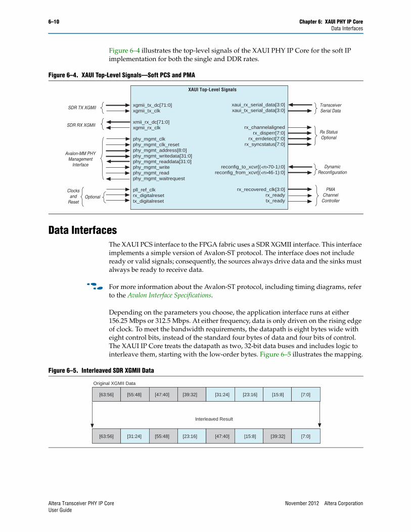
6–10 Chapter 6: XAUI PHY IP CoreData Interfaces
Figure 6–4 illustrates the top-level signals of the XAUI PHY IP Core for the soft IP implementation for both the single and DDR rates.
Data InterfacesThe XAUI PCS interface to the FPGA fabric uses a SDR XGMII interface. This interface implements a simple version of Avalon-ST protocol. The interface does not include ready or valid signals; consequently, the sources always drive data and the sinks must always be ready to receive data.
f For more information about the Avalon-ST protocol, including timing diagrams, refer to the Avalon Interface Specifications.
Depending on the parameters you choose, the application interface runs at either 156.25 Mbps or 312.5 Mbps. At either frequency, data is only driven on the rising edge of clock. To meet the bandwidth requirements, the datapath is eight bytes wide with eight control bits, instead of the standard four bytes of data and four bits of control. The XAUI IP Core treats the datapath as two, 32-bit data buses and includes logic to interleave them, starting with the low-order bytes. Figure 6–5 illustrates the mapping.
Figure 6–4. XAUI Top-Level Signals—Soft PCS and PMA
xgmii_tx_dc[71:0]xgmii_tx_clk
xmii_rx_dc[71:0]xgmii_rx_clk
phy_mgmt_clkphy_mgmt_clk_resetphy_mgmt_address[8:0]phy_mgmt_writedata[31:0]phy_mgmt_readdata[31:0]phy_mgmt_writephy_mgmt_readphy_mgmt_waitrequest
pll_ref_clkrx_digitalresettx_digitalreset
XAUI Top-Level Signals
Rx StatusOptional
xaui_rx_serial_data[3:0]xaui_tx_serial_data[3:0]
rx_channelalignedrx_disperr[7:0]
rx_errdetect[7:0]rx_syncstatus[7:0]
reconfig_to_xcvr[(<n>70-1):0]reconfig_from_xcvr[(<n>46-1):0]
rx_recovered_clk[3:0]rx_readytx_ready
TransceiverSerial Data
SDR TX XGMII
SDR RX XGMII
Avalon-MM PHYManagement
Interface
Clocksand
ResetOptional
DynamicReconfiguration
PMAChannel
Controller
Figure 6–5. Interleaved SDR XGMII Data
Interleaved Result
Original XGMII Data
[63:56] [55:48] [47:40] [39:32] [31:24] [23:16] [15:8] [7:0]
[63:56] [31:24] [55:48] [23:16] [47:40] [15:8] [39:32] [7:0]
Altera Transceiver PHY IP Core November 2012 Altera CorporationUser Guide
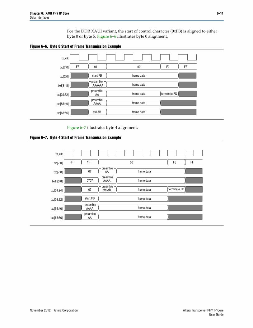
Chapter 6: XAUI PHY IP Core 6–11Data Interfaces
For the DDR XAUI variant, the start of control character (0xFB) is aligned to either byte 0 or byte 5. Figure 6–6 illustrates byte 0 alignment.
Figure 6–7 illustrates byte 4 alignment.
Figure 6–6. Byte 0 Start of Frame Transmission Example
tx_clk
txc[7:0]
txd[7:0]
txd[31:8]
txd[39:32]
txd[55:40]
txd[63:56]
FF 01 00 F0 FF
start FB
AAAA
AA
frame data
frame data
frame data terminate FD
frame data
sfd AB frame data
AAAAAApreamble
preamble
preamble
Figure 6–7. Byte 4 Start of Frame Transmission Example
tx_clk
txc[7:0]
txd[7:0]
txd[23:8]
txd[31:24]
txd[39:32]
txd[55:40]
txd[63:56]
FF 1F 00 F8 FF
07 AA frame data
0707 AAAA
AAAA
AA
frame data
07 sfd AB frame data terminate FD
start FB frame data
frame data
frame data
preamble
preamble
preamble
preamble
preamble
November 2012 Altera Corporation Altera Transceiver PHY IP CoreUser Guide
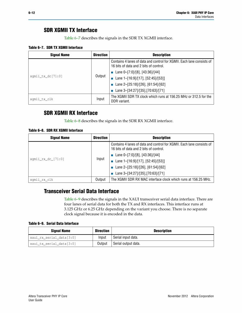
6–12 Chapter 6: XAUI PHY IP CoreData Interfaces
SDR XGMII TX InterfaceTable 6–7 describes the signals in the SDR TX XGMII interface.
SDR XGMII RX InterfaceTable 6–8 describes the signals in the SDR RX XGMII interface.
Transceiver Serial Data InterfaceTable 6–9 describes the signals in the XAUI transceiver serial data interface. There are four lanes of serial data for both the TX and RX interfaces. This interface runs at 3.125 GHz or 6.25 GHz depending on the variant you choose. There is no separate clock signal because it is encoded in the data.
Table 6–7. SDR TX XGMII Interface
Signal Name Direction Description
xgmii_tx_dc[71:0] Output
Contains 4 lanes of data and control for XGMII. Each lane consists of 16 bits of data and 2 bits of control.
■ Lane 0–[7:0]/[8], [43:36]/[44]
■ Lane 1–[16:9]/[17], [52:45]/[53]]
■ Lane 2–[25:18]/[26], [61:54]/[62]
■ Lane 3–[34:27]/[35],[70:63]/[71]
xgmii_tx_clk Input The XGMII SDR TX clock which runs at 156.25 MHz or 312.5 for the DDR variant.
Table 6–8. SDR RX XGMII Interface
Signal Name Direction Description
xgmii_rx_dc_[71:0] Input
Contains 4 lanes of data and control for XGMII. Each lane consists of 16 bits of data and 2 bits of control.
■ Lane 0–[7:0]/[8], [43:36]/[44]
■ Lane 1–[16:9]/[17], [52:45]/[53]]
■ Lane 2–[25:18]/[26], [61:54]/[62]
■ Lane 3–[34:27]/[35],[70:63]/[71]
xgmii_rx_clk Output The XGMII SDR RX MAC interface clock which runs at 156.25 MHz.
Table 6–9. Serial Data Interface
Signal Name Direction Description
xaui_rx_serial_data[3:0] Input Serial input data.
xaui_tx_serial_data[3:0] Output Serial output data.
Altera Transceiver PHY IP Core November 2012 Altera CorporationUser Guide
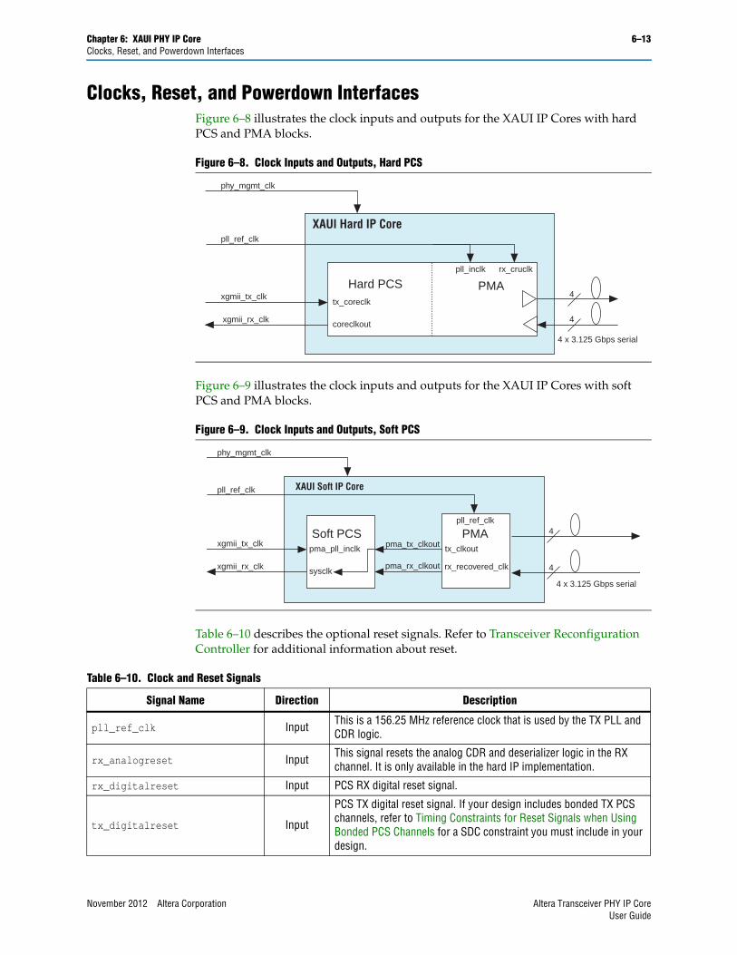
Chapter 6: XAUI PHY IP Core 6–13Clocks, Reset, and Powerdown Interfaces
Clocks, Reset, and Powerdown InterfacesFigure 6–8 illustrates the clock inputs and outputs for the XAUI IP Cores with hard PCS and PMA blocks.
Figure 6–9 illustrates the clock inputs and outputs for the XAUI IP Cores with soft PCS and PMA blocks.
Table 6–10 describes the optional reset signals. Refer to Transceiver Reconfiguration Controller for additional information about reset.
Figure 6–8. Clock Inputs and Outputs, Hard PCS
Figure 6–9. Clock Inputs and Outputs, Soft PCS
XAUI Hard IP Core
4 x 3.125 Gbps serial
Hard PCStx_coreclk
rx_cruclkpll_inclk
coreclkoutxgmii_rx_clk
xgmii_tx_clk
pll_ref_clk
phy_mgmt_clk
4
4 PMA
XAUI Soft IP Core
4 x 3.125 Gbps serial
xgmii_rx_clk
xgmii_tx_clk
pll_ref_clk
phy_mgmt_clk
4
4Soft PCSpma_pll_inclk pma_tx_clkout tx_clkout
pma_rx_clkout
pll_ref_clk
sysclk
PMA
rx_recovered_clk
Table 6–10. Clock and Reset Signals
Signal Name Direction Description
pll_ref_clk Input This is a 156.25 MHz reference clock that is used by the TX PLL and CDR logic.
rx_analogreset Input This signal resets the analog CDR and deserializer logic in the RX channel. It is only available in the hard IP implementation.
rx_digitalreset Input PCS RX digital reset signal.
tx_digitalreset Input
PCS TX digital reset signal. If your design includes bonded TX PCS channels, refer to Timing Constraints for Reset Signals when Using Bonded PCS Channels for a SDC constraint you must include in your design.
November 2012 Altera Corporation Altera Transceiver PHY IP CoreUser Guide
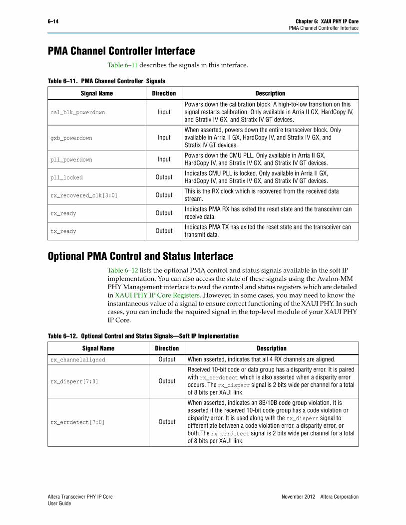
6–14 Chapter 6: XAUI PHY IP CorePMA Channel Controller Interface
PMA Channel Controller InterfaceTable 6–11 describes the signals in this interface.
Optional PMA Control and Status Interface Table 6–12 lists the optional PMA control and status signals available in the soft IP implementation. You can also access the state of these signals using the Avalon-MM PHY Management interface to read the control and status registers which are detailed in XAUI PHY IP Core Registers. However, in some cases, you may need to know the instantaneous value of a signal to ensure correct functioning of the XAUI PHY. In such cases, you can include the required signal in the top-level module of your XAUI PHY IP Core.
Table 6–11. PMA Channel Controller Signals
Signal Name Direction Description
cal_blk_powerdown InputPowers down the calibration block. A high-to-low transition on this signal restarts calibration. Only available in Arria II GX, HardCopy IV, and Stratix IV GX, and Stratix IV GT devices.
gxb_powerdown InputWhen asserted, powers down the entire transceiver block. Only available in Arria II GX, HardCopy IV, and Stratix IV GX, and Stratix IV GT devices.
pll_powerdown Input Powers down the CMU PLL. Only available in Arria II GX, HardCopy IV, and Stratix IV GX, and Stratix IV GT devices.
pll_locked Output Indicates CMU PLL is locked. Only available in Arria II GX, HardCopy IV, and Stratix IV GX, and Stratix IV GT devices.
rx_recovered_clk[3:0] Output This is the RX clock which is recovered from the received data stream.
rx_ready Output Indicates PMA RX has exited the reset state and the transceiver can receive data.
tx_ready Output Indicates PMA TX has exited the reset state and the transceiver can transmit data.
Table 6–12. Optional Control and Status Signals—Soft IP Implementation
Signal Name Direction Description
rx_channelaligned Output When asserted, indicates that all 4 RX channels are aligned.
rx_disperr[7:0] Output
Received 10-bit code or data group has a disparity error. It is paired with rx_errdetect which is also asserted when a disparity error occurs. The rx_disperr signal is 2 bits wide per channel for a total of 8 bits per XAUI link.
rx_errdetect[7:0] Output
When asserted, indicates an 8B/10B code group violation. It is asserted if the received 10-bit code group has a code violation or disparity error. It is used along with the rx_disperr signal to differentiate between a code violation error, a disparity error, or both.The rx_errdetect signal is 2 bits wide per channel for a total of 8 bits per XAUI link.
Altera Transceiver PHY IP Core November 2012 Altera CorporationUser Guide
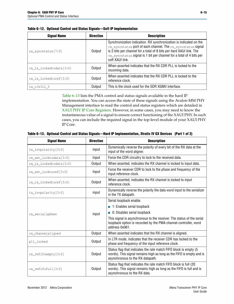
Chapter 6: XAUI PHY IP Core 6–15Optional PMA Control and Status Interface
Table 6–13 lists the PMA control and status signals available in the hard IP implementation. You can access the state of these signals using the Avalon-MM PHY Management interface to read the control and status registers which are detailed in XAUI PHY IP Core Registers. However, in some cases, you may need to know the instantaneous value of a signal to ensure correct functioning of the XAUI PHY. In such cases, you can include the required signal in the top-level module of your XAUI PHY IP Core.
rx_syncstatus[7:0] Output
Synchronization indication. RX synchronization is indicated on the rx_syncstatus port of each channel. The rx_syncstatus signal is 2 bits per channel for a total of 8 bits per hard XAUI link. The rx_syncstatus signal is 1 bit per channel for a total of 4 bits per soft XAUI link.
rx_is_lockedtodata[3:0] Output When asserted indicates that the RX CDR PLL is locked to the incoming data.
rx_is_lockedtoref[3:0] Output When asserted indicates that the RX CDR PLL is locked to the reference clock.
tx_clk312_5 Output This is the clock used for the SDR XGMII interface.
Table 6–12. Optional Control and Status Signals—Soft IP Implementation
Signal Name Direction Description
Table 6–13. Optional Control and Status Signals—Hard IP Implementation, Stratix IV GX Devices (Part 1 of 2)
Signal Name Direction Description
rx_invpolarity[3:0] input Dynamically reverse the polarity of every bit of the RX data at the input of the word aligner.
rx_set_locktodata[3:0] Input Force the CDR circuitry to lock to the received data.
rx_is_lockedtodata[3:0] Output When asserted, indicates the RX channel is locked to input data.
rx_set_locktoref[3:0] Input Force the receiver CDR to lock to the phase and frequency of the input reference clock.
rx_is_lockedtoref[3:0] Output When asserted, indicates the RX channel is locked to input reference clock.
tx_invpolarity[3:0] input Dynamically reverse the polarity the data word input to the serializer in the TX datapath.
rx_seriallpbken input
Serial loopback enable.
■ 1: Enables serial loopback
■ 0: Disables serial loopback
This signal is asynchronous to the receiver. The status of the serial loopback option is recorded by the PMA channel controller, word address 0x061.
rx_channelaligned Output When asserted indicates that the RX channel is aligned.
pll_locked Output In LTR mode, indicates that the receiver CDR has locked to the phase and frequency of the input reference clock.
rx_rmfifoempty[3:0] OutputStatus flag that indicates the rate match FIFO block is empty (5 words). This signal remains high as long as the FIFO is empty and is asynchronous to the RX datapath.
rx_rmfifofull[3:0] OutputStatus flag that indicates the rate match FIFO block is full (20 words). This signal remains high as long as the FIFO is full and is asynchronous to the RX data.
November 2012 Altera Corporation Altera Transceiver PHY IP CoreUser Guide
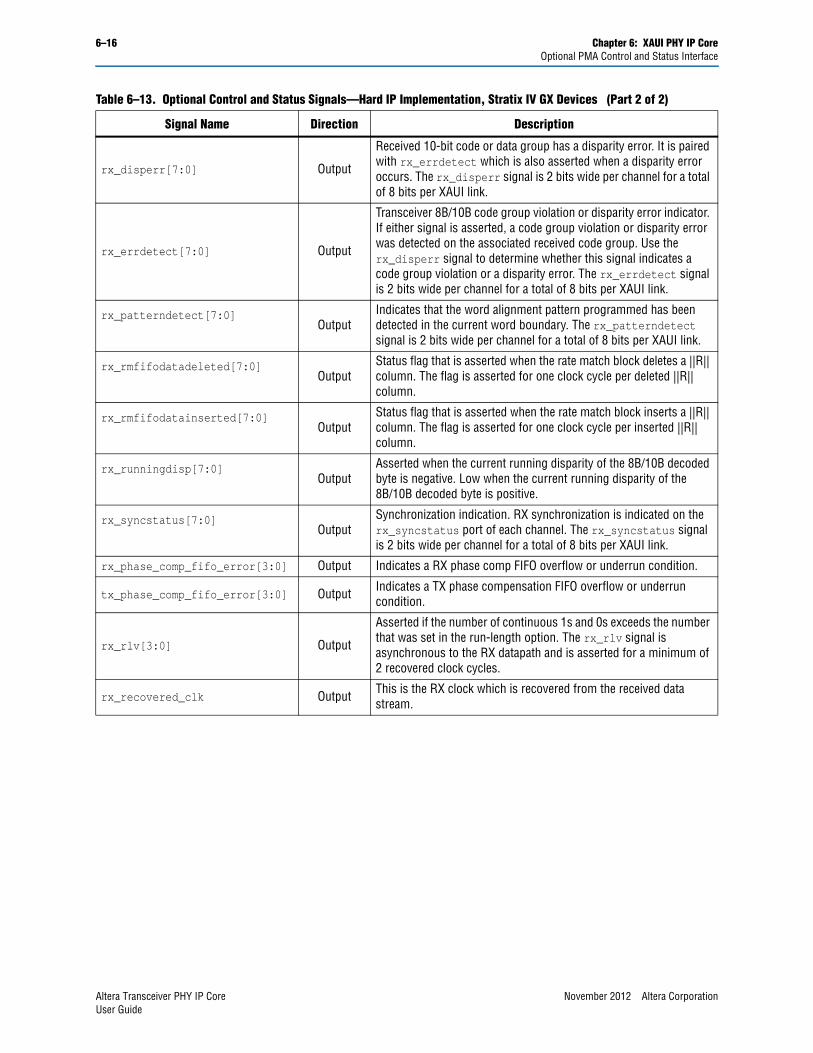
6–16 Chapter 6: XAUI PHY IP CoreOptional PMA Control and Status Interface
rx_disperr[7:0] Output
Received 10-bit code or data group has a disparity error. It is paired with rx_errdetect which is also asserted when a disparity error occurs. The rx_disperr signal is 2 bits wide per channel for a total of 8 bits per XAUI link.
rx_errdetect[7:0] Output
Transceiver 8B/10B code group violation or disparity error indicator. If either signal is asserted, a code group violation or disparity error was detected on the associated received code group. Use the rx_disperr signal to determine whether this signal indicates a code group violation or a disparity error. The rx_errdetect signal is 2 bits wide per channel for a total of 8 bits per XAUI link.
rx_patterndetect[7:0]Output
Indicates that the word alignment pattern programmed has been detected in the current word boundary. The rx_patterndetect signal is 2 bits wide per channel for a total of 8 bits per XAUI link.
rx_rmfifodatadeleted[7:0]Output
Status flag that is asserted when the rate match block deletes a ||R|| column. The flag is asserted for one clock cycle per deleted ||R|| column.
rx_rmfifodatainserted[7:0]Output
Status flag that is asserted when the rate match block inserts a ||R|| column. The flag is asserted for one clock cycle per inserted ||R|| column.
rx_runningdisp[7:0]Output
Asserted when the current running disparity of the 8B/10B decoded byte is negative. Low when the current running disparity of the 8B/10B decoded byte is positive.
rx_syncstatus[7:0]Output
Synchronization indication. RX synchronization is indicated on the rx_syncstatus port of each channel. The rx_syncstatus signal is 2 bits wide per channel for a total of 8 bits per XAUI link.
rx_phase_comp_fifo_error[3:0] Output Indicates a RX phase comp FIFO overflow or underrun condition.
tx_phase_comp_fifo_error[3:0] Output Indicates a TX phase compensation FIFO overflow or underrun condition.
rx_rlv[3:0] Output
Asserted if the number of continuous 1s and 0s exceeds the number that was set in the run-length option. The rx_rlv signal is asynchronous to the RX datapath and is asserted for a minimum of 2 recovered clock cycles.
rx_recovered_clk Output This is the RX clock which is recovered from the received data stream.
Table 6–13. Optional Control and Status Signals—Hard IP Implementation, Stratix IV GX Devices (Part 2 of 2)
Signal Name Direction Description
Altera Transceiver PHY IP Core November 2012 Altera CorporationUser Guide
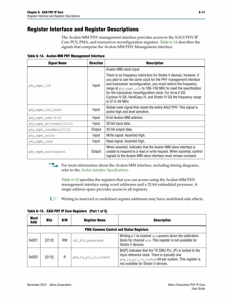
Chapter 6: XAUI PHY IP Core 6–17Register Interface and Register Descriptions
Register Interface and Register DescriptionsThe Avalon-MM PHY management interface provides access to the XAUI PHY IP Core PCS, PMA, and transceiver reconfiguration registers. Table 6–14 describes the signals that comprise the Avalon-MM PHY Management interface.
f For more information about the Avalon-MM interface, including timing diagrams, refer to the Avalon Interface Specifications.
Table 6–15 specifies the registers that you can access using the Avalon-MM PHY management interface using word addresses and a 32-bit embedded processor. A single address space provides access to all registers.
1 Writing to reserved or undefined register addresses may have undefined side effects.
Table 6–14. Avalon-MM PHY Management Interface
Signal Name Direction Description
phy_mgmt_clk Input
Avalon-MM clock input.
There is no frequency restriction for Stratix V devices; however, if you plan to use the same clock for the PHY management interface and transceiver reconfiguration, you must restrict the frequency range of phy_mgmt_clk to 100–150 MHz to meet the specification for the transceiver reconfiguration clock. For Arria II GX, Cyclone IV GX, HardCopy IV, and Stratix IV GX the frequency range is 37.5–50 MHz.
phy_mgmt_clk_reset Input Global reset signal that resets the entire XAUI PHY. This signal is active high and level sensitive.
phy_mgmt_addr[8:0] Input 9-bit Avalon-MM address.
phy_mgmt_writedata[31:0] Input 32-bit input data.
phy_mgmt_readdata[31:0] Output 32-bit output data.
phy_mgmt_write Input Write signal. Asserted high.
phy_mgmt_read Input Read signal. Asserted high.
phy_mgmt_waitrequest OutputWhen asserted, indicates that the Avalon-MM slave interface is unable to respond to a read or write request. When asserted, control signals to the Avalon-MM slave interface must remain constant.
Table 6–15. XAUI PHY IP Core Registers (Part 1 of 5)
Word Addr Bits R/W Register Name Description
PMA Common Control and Status Registers
0x021 [31:0] RW cal_blk_powerdownWriting a 1 to channel <n> powers down the calibration block for channel <n>. This register is not available for Stratix V devices.
0x022 [31:0] R pma_tx_pll_is_locked
Bit[P] indicates that the TX CMU PLL (P) is locked to the input reference clock. There is typically one pma_tx_pll_is_locked bit per system. This register is not available for Stratix V devices.
November 2012 Altera Corporation Altera Transceiver PHY IP CoreUser Guide
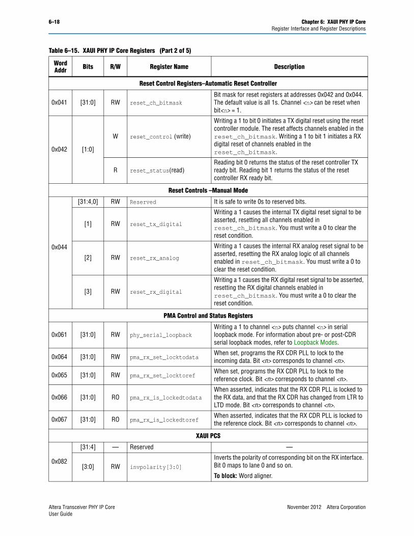
6–18 Chapter 6: XAUI PHY IP CoreRegister Interface and Register Descriptions
Reset Control Registers–Automatic Reset Controller
0x041 [31:0] RW reset_ch_bitmaskBit mask for reset registers at addresses 0x042 and 0x044. The default value is all 1s. Channel <n> can be reset when bit<n> = 1.
0x042 [1:0]
W reset_control (write)
Writing a 1 to bit 0 initiates a TX digital reset using the reset controller module. The reset affects channels enabled in the reset_ch_bitmask. Writing a 1 to bit 1 initiates a RX digital reset of channels enabled in the reset_ch_bitmask.
R reset_status(read)Reading bit 0 returns the status of the reset controller TX ready bit. Reading bit 1 returns the status of the reset controller RX ready bit.
Reset Controls –Manual Mode
0x044
[31:4,0] RW Reserved It is safe to write 0s to reserved bits.
[1] RW reset_tx_digital
Writing a 1 causes the internal TX digital reset signal to be asserted, resetting all channels enabled in reset_ch_bitmask. You must write a 0 to clear the reset condition.
[2] RW reset_rx_analog
Writing a 1 causes the internal RX analog reset signal to be asserted, resetting the RX analog logic of all channels enabled in reset_ch_bitmask. You must write a 0 to clear the reset condition.
[3] RW reset_rx_digital
Writing a 1 causes the RX digital reset signal to be asserted, resetting the RX digital channels enabled in reset_ch_bitmask. You must write a 0 to clear the reset condition.
PMA Control and Status Registers
0x061 [31:0] RW phy_serial_loopbackWriting a 1 to channel <n> puts channel <n> in serial loopback mode. For information about pre- or post-CDR serial loopback modes, refer to Loopback Modes.
0x064 [31:0] RW pma_rx_set_locktodataWhen set, programs the RX CDR PLL to lock to the incoming data. Bit <n> corresponds to channel <n>.
0x065 [31:0] RW pma_rx_set_locktorefWhen set, programs the RX CDR PLL to lock to the reference clock. Bit <n> corresponds to channel <n>.
0x066 [31:0] RO pma_rx_is_lockedtodataWhen asserted, indicates that the RX CDR PLL is locked to the RX data, and that the RX CDR has changed from LTR to LTD mode. Bit <n> corresponds to channel <n>.
0x067 [31:0] RO pma_rx_is_lockedtorefWhen asserted, indicates that the RX CDR PLL is locked to the reference clock. Bit <n> corresponds to channel <n>.
XAUI PCS
0x082
[31:4] — Reserved —
[3:0] RW invpolarity[3:0]
Inverts the polarity of corresponding bit on the RX interface. Bit 0 maps to lane 0 and so on.
To block: Word aligner.
Table 6–15. XAUI PHY IP Core Registers (Part 2 of 5)
Word Addr Bits R/W Register Name Description
Altera Transceiver PHY IP Core November 2012 Altera CorporationUser Guide
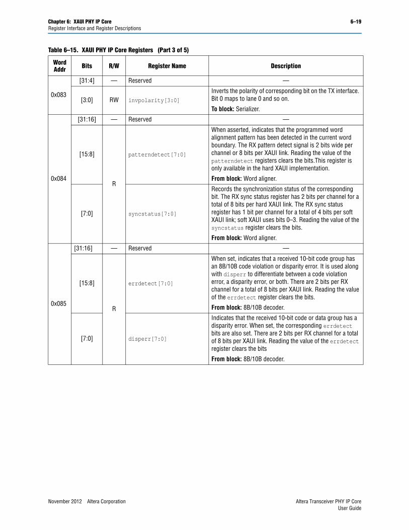
Chapter 6: XAUI PHY IP Core 6–19Register Interface and Register Descriptions
0x083
[31:4] — Reserved —
[3:0] RW invpolarity[3:0]
Inverts the polarity of corresponding bit on the TX interface. Bit 0 maps to lane 0 and so on.
To block: Serializer.
0x084
[31:16] — Reserved —
[15:8]
R
patterndetect[7:0]
When asserted, indicates that the programmed word alignment pattern has been detected in the current word boundary. The RX pattern detect signal is 2 bits wide per channel or 8 bits per XAUI link. Reading the value of the patterndetect registers clears the bits.This register is only available in the hard XAUI implementation.
From block: Word aligner.
[7:0] syncstatus[7:0]
Records the synchronization status of the corresponding bit. The RX sync status register has 2 bits per channel for a total of 8 bits per hard XAUI link. The RX sync status register has 1 bit per channel for a total of 4 bits per soft XAUI link; soft XAUI uses bits 0–3. Reading the value of the syncstatus register clears the bits.
From block: Word aligner.
0x085
[31:16] — Reserved —
[15:8]
R
errdetect[7:0]
When set, indicates that a received 10-bit code group has an 8B/10B code violation or disparity error. It is used along with disperr to differentiate between a code violation error, a disparity error, or both. There are 2 bits per RX channel for a total of 8 bits per XAUI link. Reading the value of the errdetect register clears the bits.
From block: 8B/10B decoder.
[7:0] disperr[7:0]
Indicates that the received 10-bit code or data group has a disparity error. When set, the corresponding errdetect bits are also set. There are 2 bits per RX channel for a total of 8 bits per XAUI link. Reading the value of the errdetect register clears the bits
From block: 8B/10B decoder.
Table 6–15. XAUI PHY IP Core Registers (Part 3 of 5)
Word Addr Bits R/W Register Name Description
November 2012 Altera Corporation Altera Transceiver PHY IP CoreUser Guide
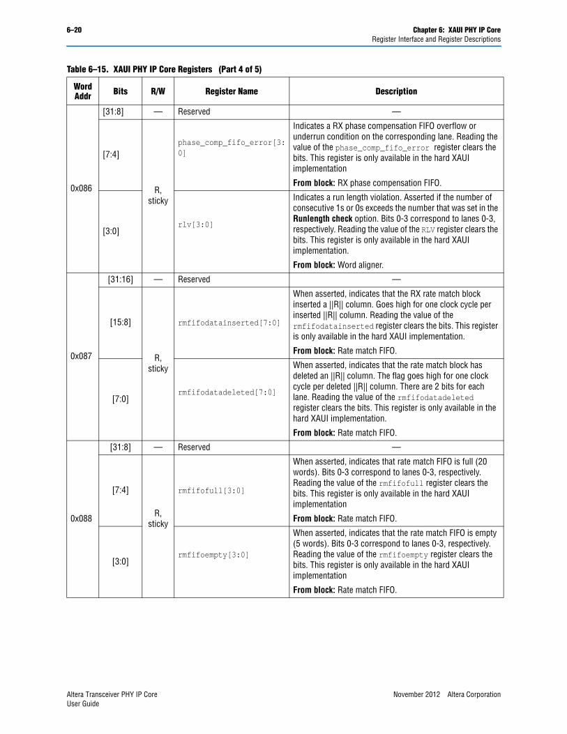
6–20 Chapter 6: XAUI PHY IP CoreRegister Interface and Register Descriptions
0x086
[31:8] — Reserved —
[7:4]
R, sticky
phase_comp_fifo_error[3:0]
Indicates a RX phase compensation FIFO overflow or underrun condition on the corresponding lane. Reading the value of the phase_comp_fifo_error register clears the bits. This register is only available in the hard XAUI implementation
From block: RX phase compensation FIFO.
[3:0]rlv[3:0]
Indicates a run length violation. Asserted if the number of consecutive 1s or 0s exceeds the number that was set in the Runlength check option. Bits 0-3 correspond to lanes 0-3, respectively. Reading the value of the RLV register clears the bits. This register is only available in the hard XAUI implementation.
From block: Word aligner.
0x087
[31:16] — Reserved —
[15:8]
R, sticky
rmfifodatainserted[7:0]
When asserted, indicates that the RX rate match block inserted a ||R|| column. Goes high for one clock cycle per inserted ||R|| column. Reading the value of the rmfifodatainserted register clears the bits. This register is only available in the hard XAUI implementation.
From block: Rate match FIFO.
[7:0]rmfifodatadeleted[7:0]
When asserted, indicates that the rate match block has deleted an ||R|| column. The flag goes high for one clock cycle per deleted ||R|| column. There are 2 bits for each lane. Reading the value of the rmfifodatadeleted register clears the bits. This register is only available in the hard XAUI implementation.
From block: Rate match FIFO.
0x088
[31:8] — Reserved —
[7:4]
R, sticky
rmfifofull[3:0]
When asserted, indicates that rate match FIFO is full (20 words). Bits 0-3 correspond to lanes 0-3, respectively. Reading the value of the rmfifofull register clears the bits. This register is only available in the hard XAUI implementation
From block: Rate match FIFO.
[3:0]rmfifoempty[3:0]
When asserted, indicates that the rate match FIFO is empty (5 words). Bits 0-3 correspond to lanes 0-3, respectively. Reading the value of the rmfifoempty register clears the bits. This register is only available in the hard XAUI implementation
From block: Rate match FIFO.
Table 6–15. XAUI PHY IP Core Registers (Part 4 of 5)
Word Addr Bits R/W Register Name Description
Altera Transceiver PHY IP Core November 2012 Altera CorporationUser Guide
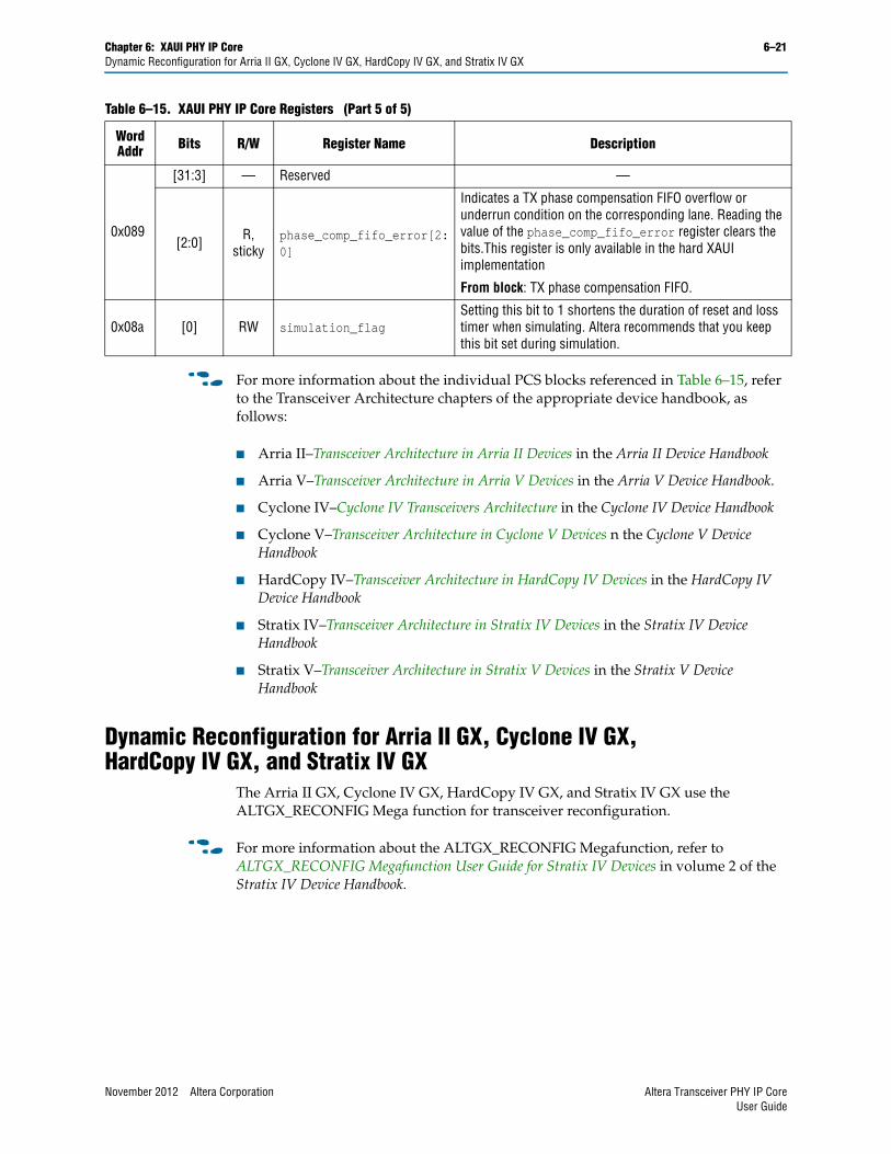
Chapter 6: XAUI PHY IP Core 6–21Dynamic Reconfiguration for Arria II GX, Cyclone IV GX, HardCopy IV GX, and Stratix IV GX
f For more information about the individual PCS blocks referenced in Table 6–15, refer to the Transceiver Architecture chapters of the appropriate device handbook, as follows:
■ Arria II–Transceiver Architecture in Arria II Devices in the Arria II Device Handbook
■ Arria V–Transceiver Architecture in Arria V Devices in the Arria V Device Handbook.
■ Cyclone IV–Cyclone IV Transceivers Architecture in the Cyclone IV Device Handbook
■ Cyclone V–Transceiver Architecture in Cyclone V Devices n the Cyclone V Device Handbook
■ HardCopy IV–Transceiver Architecture in HardCopy IV Devices in the HardCopy IV Device Handbook
■ Stratix IV–Transceiver Architecture in Stratix IV Devices in the Stratix IV Device Handbook
■ Stratix V–Transceiver Architecture in Stratix V Devices in the Stratix V Device Handbook
Dynamic Reconfiguration for Arria II GX, Cyclone IV GX, HardCopy IV GX, and Stratix IV GX
The Arria II GX, Cyclone IV GX, HardCopy IV GX, and Stratix IV GX use the ALTGX_RECONFIG Mega function for transceiver reconfiguration.
f For more information about the ALTGX_RECONFIG Megafunction, refer to ALTGX_RECONFIG Megafunction User Guide for Stratix IV Devices in volume 2 of the Stratix IV Device Handbook.
0x089
[31:3] — Reserved —
[2:0] R, sticky
phase_comp_fifo_error[2:0]
Indicates a TX phase compensation FIFO overflow or underrun condition on the corresponding lane. Reading the value of the phase_comp_fifo_error register clears the bits.This register is only available in the hard XAUI implementation
From block: TX phase compensation FIFO.
0x08a [0] RW simulation_flagSetting this bit to 1 shortens the duration of reset and loss timer when simulating. Altera recommends that you keep this bit set during simulation.
Table 6–15. XAUI PHY IP Core Registers (Part 5 of 5)
Word Addr Bits R/W Register Name Description
November 2012 Altera Corporation Altera Transceiver PHY IP CoreUser Guide
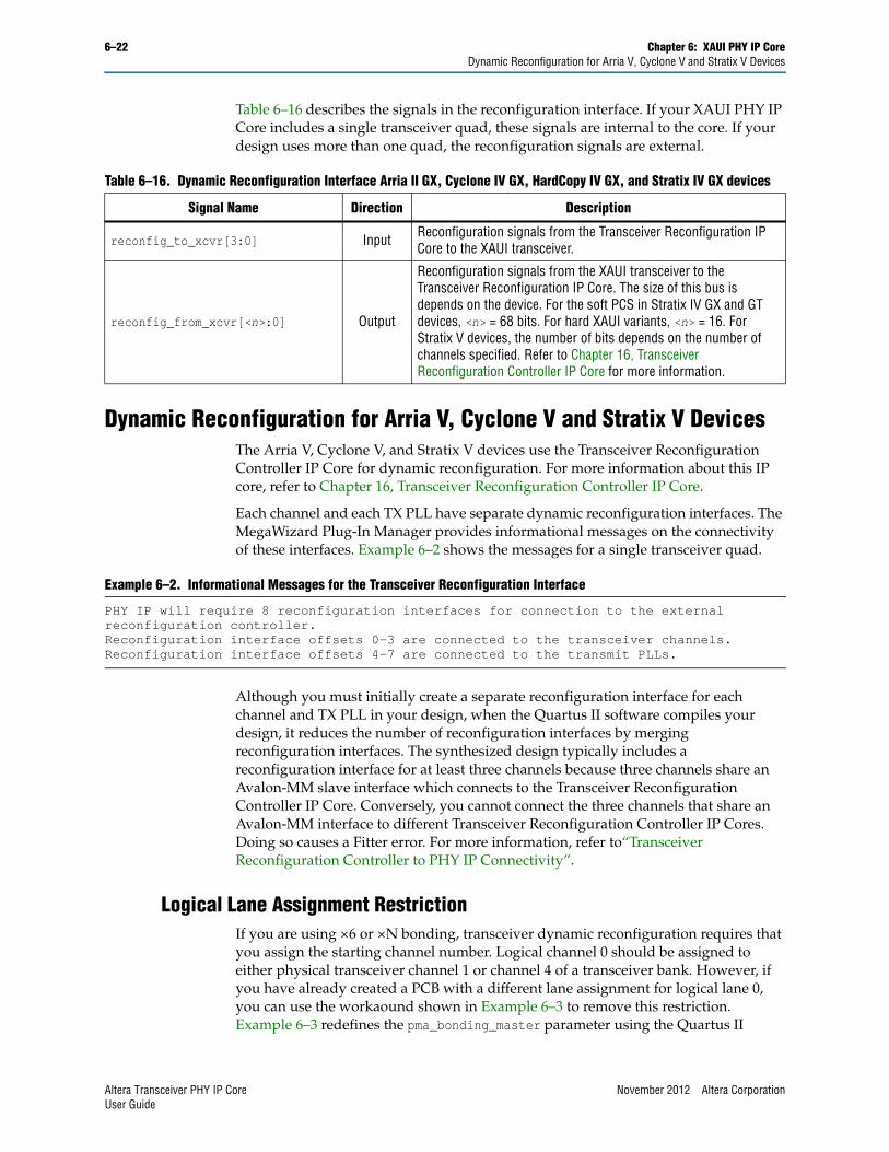
6–22 Chapter 6: XAUI PHY IP CoreDynamic Reconfiguration for Arria V, Cyclone V and Stratix V Devices
Table 6–16 describes the signals in the reconfiguration interface. If your XAUI PHY IP Core includes a single transceiver quad, these signals are internal to the core. If your design uses more than one quad, the reconfiguration signals are external.
Dynamic Reconfiguration for Arria V, Cyclone V and Stratix V DevicesThe Arria V, Cyclone V, and Stratix V devices use the Transceiver Reconfiguration Controller IP Core for dynamic reconfiguration. For more information about this IP core, refer to Chapter 16, Transceiver Reconfiguration Controller IP Core.
Each channel and each TX PLL have separate dynamic reconfiguration interfaces. The MegaWizard Plug-In Manager provides informational messages on the connectivity of these interfaces. Example 6–2 shows the messages for a single transceiver quad.
Although you must initially create a separate reconfiguration interface for each channel and TX PLL in your design, when the Quartus II software compiles your design, it reduces the number of reconfiguration interfaces by merging reconfiguration interfaces. The synthesized design typically includes a reconfiguration interface for at least three channels because three channels share an Avalon-MM slave interface which connects to the Transceiver Reconfiguration Controller IP Core. Conversely, you cannot connect the three channels that share an Avalon-MM interface to different Transceiver Reconfiguration Controller IP Cores. Doing so causes a Fitter error. For more information, refer to“Transceiver Reconfiguration Controller to PHY IP Connectivity”.
Logical Lane Assignment Restriction If you are using ×6 or ×N bonding, transceiver dynamic reconfiguration requires that you assign the starting channel number. Logical channel 0 should be assigned to either physical transceiver channel 1 or channel 4 of a transceiver bank. However, if you have already created a PCB with a different lane assignment for logical lane 0, you can use the workaound shown in Example 6–3 to remove this restriction. Example 6–3 redefines the pma_bonding_master parameter using the Quartus II
Table 6–16. Dynamic Reconfiguration Interface Arria II GX, Cyclone IV GX, HardCopy IV GX, and Stratix IV GX devices
Signal Name Direction Description
reconfig_to_xcvr[3:0] Input Reconfiguration signals from the Transceiver Reconfiguration IP Core to the XAUI transceiver.
reconfig_from_xcvr[<n>:0] Output
Reconfiguration signals from the XAUI transceiver to the Transceiver Reconfiguration IP Core. The size of this bus is depends on the device. For the soft PCS in Stratix IV GX and GT devices, <n> = 68 bits. For hard XAUI variants, <n> = 16. For Stratix V devices, the number of bits depends on the number of channels specified. Refer to Chapter 16, Transceiver Reconfiguration Controller IP Core for more information.
Example 6–2. Informational Messages for the Transceiver Reconfiguration Interface
PHY IP will require 8 reconfiguration interfaces for connection to the external reconfiguration controller.Reconfiguration interface offsets 0-3 are connected to the transceiver channels.Reconfiguration interface offsets 4-7 are connected to the transmit PLLs.
Altera Transceiver PHY IP Core November 2012 Altera CorporationUser Guide
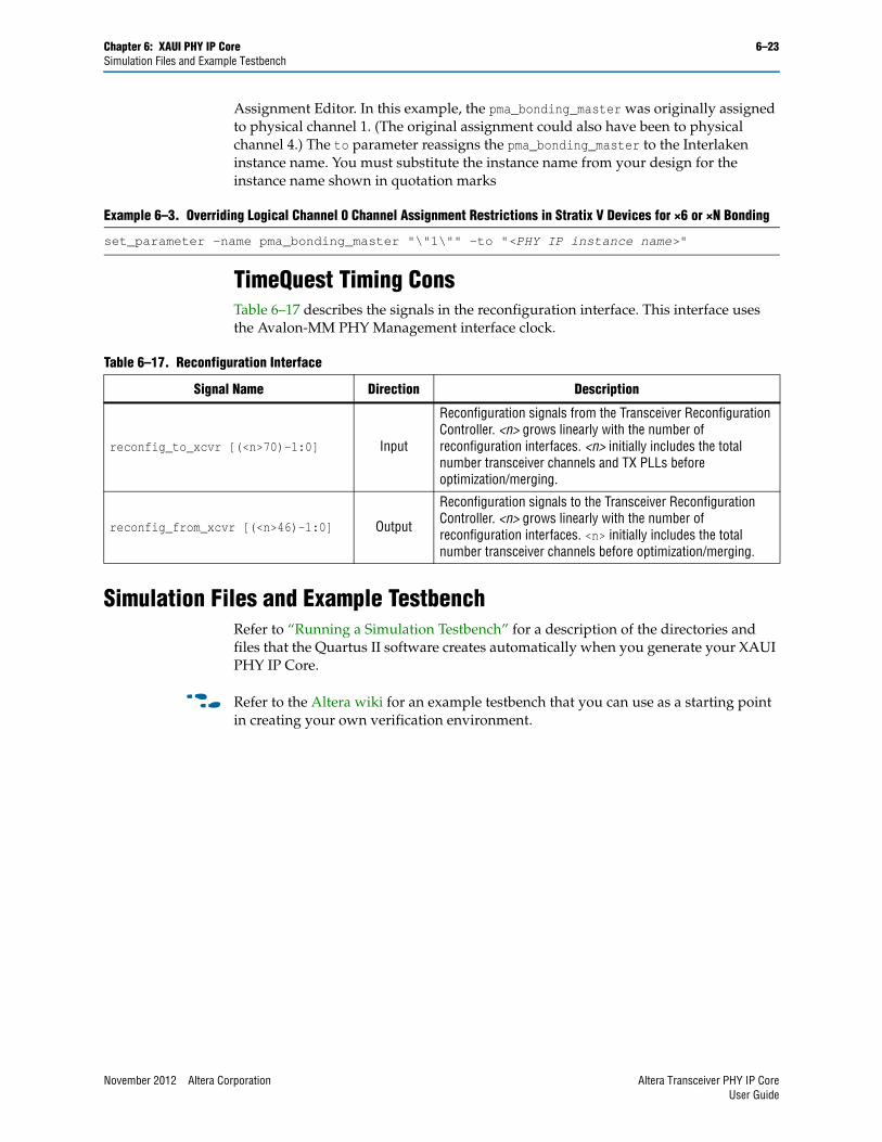
Chapter 6: XAUI PHY IP Core 6–23Simulation Files and Example Testbench
Assignment Editor. In this example, the pma_bonding_master was originally assigned to physical channel 1. (The original assignment could also have been to physical channel 4.) The to parameter reassigns the pma_bonding_master to the Interlaken instance name. You must substitute the instance name from your design for the instance name shown in quotation marks
TimeQuest Timing ConsTable 6–17 describes the signals in the reconfiguration interface. This interface uses the Avalon-MM PHY Management interface clock.
Simulation Files and Example TestbenchRefer to “Running a Simulation Testbench” for a description of the directories and files that the Quartus II software creates automatically when you generate your XAUI PHY IP Core.
f Refer to the Altera wiki for an example testbench that you can use as a starting point in creating your own verification environment.
Example 6–3. Overriding Logical Channel 0 Channel Assignment Restrictions in Stratix V Devices for ×6 or ×N Bonding
set_parameter -name pma_bonding_master "\"1\"" -to "<PHY IP instance name>"
Table 6–17. Reconfiguration Interface
Signal Name Direction Description
reconfig_to_xcvr [(<n>70)-1:0] Input
Reconfiguration signals from the Transceiver Reconfiguration Controller. <n> grows linearly with the number of reconfiguration interfaces. <n> initially includes the total number transceiver channels and TX PLLs before optimization/merging.
reconfig_from_xcvr [(<n>46)-1:0] Output
Reconfiguration signals to the Transceiver Reconfiguration Controller. <n> grows linearly with the number of reconfiguration interfaces. <n> initially includes the total number transceiver channels before optimization/merging.
November 2012 Altera Corporation Altera Transceiver PHY IP CoreUser Guide

6–24 Chapter 6: XAUI PHY IP CoreSimulation Files and Example Testbench
Altera Transceiver PHY IP Core November 2012 Altera CorporationUser Guide
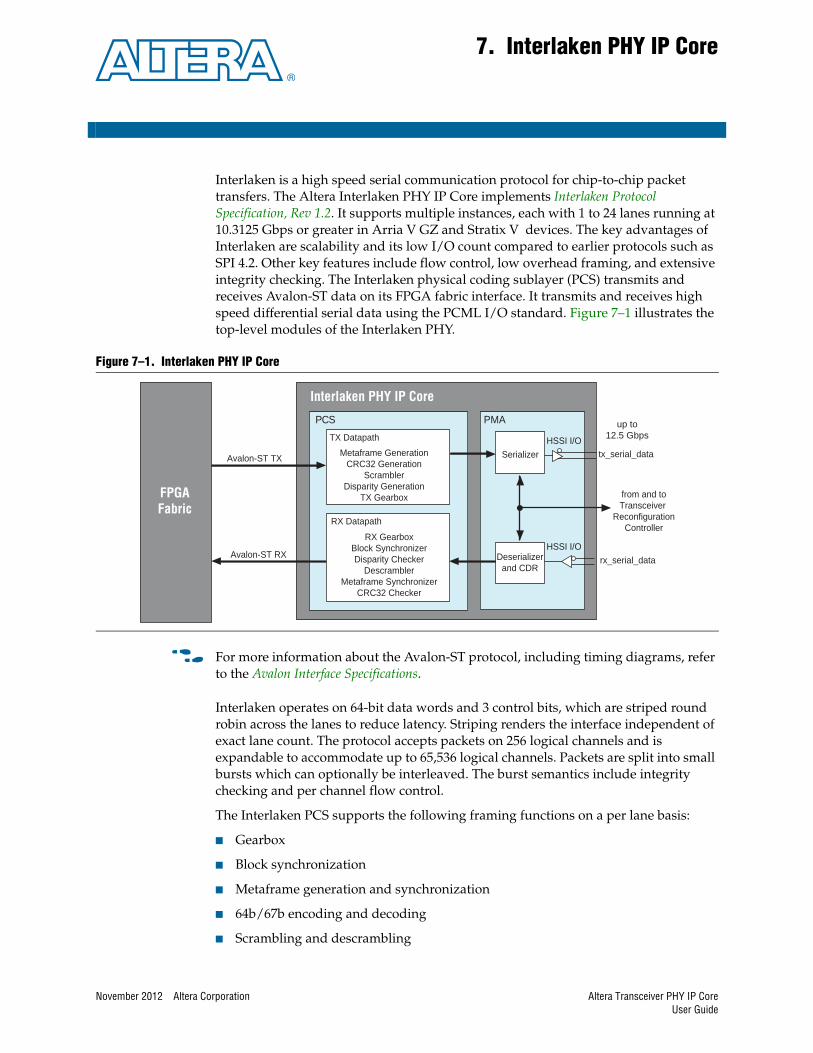
November 2012 Altera Corporation
7. Interlaken PHY IP Core
Interlaken is a high speed serial communication protocol for chip-to-chip packet transfers. The Altera Interlaken PHY IP Core implements Interlaken Protocol Specification, Rev 1.2. It supports multiple instances, each with 1 to 24 lanes running at 10.3125 Gbps or greater in Arria V GZ and Stratix V devices. The key advantages of Interlaken are scalability and its low I/O count compared to earlier protocols such as SPI 4.2. Other key features include flow control, low overhead framing, and extensive integrity checking. The Interlaken physical coding sublayer (PCS) transmits and receives Avalon-ST data on its FPGA fabric interface. It transmits and receives high speed differential serial data using the PCML I/O standard. Figure 7–1 illustrates the top-level modules of the Interlaken PHY.
f For more information about the Avalon-ST protocol, including timing diagrams, refer to the Avalon Interface Specifications.
Interlaken operates on 64-bit data words and 3 control bits, which are striped round robin across the lanes to reduce latency. Striping renders the interface independent of exact lane count. The protocol accepts packets on 256 logical channels and is expandable to accommodate up to 65,536 logical channels. Packets are split into small bursts which can optionally be interleaved. The burst semantics include integrity checking and per channel flow control.
The Interlaken PCS supports the following framing functions on a per lane basis:
■ Gearbox
■ Block synchronization
■ Metaframe generation and synchronization
■ 64b/67b encoding and decoding
■ Scrambling and descrambling
Figure 7–1. Interlaken PHY IP Core
PCS PMA
Serializer
Deserializerand CDR
HSSI I/O
HSSI I/O
Interlaken PHY IP Core
FPGAFabric
tx_serial_data
from and toTransceiver
ReconfigurationController
Avalon-ST TX
Avalon-ST RXrx_serial_data
up to 12.5 Gbps
Metaframe GenerationCRC32 Generation
ScramblerDisparity Generation
TX Gearbox
TX Datapath
RX GearboxBlock SynchronizerDisparity Checker
DescramblerMetaframe Synchronizer
CRC32 Checker
RX Datapath
Altera Transceiver PHY IP CoreUser Guide
7–2 Chapter 7: Interlaken PHY IP CoreDevice Family Support
■ Lane-based CRC32
■ Disparity DC balancing
f For more detailed information about the Interlaken transceiver channel datapath, clocking, and channel placement in Stratix V devices, refer to the “Interlaken” section in the Transceiver Configurations in Stratix V Devices chapter of the Stratix V Device Handbook.
f For more detailed information about the Interlaken transceiver channel datapath, clocking, and channel placement in Arria V GZ devices, refer to the “Interlaken” section in the Transceiver Configurations in Arria V Devices chapter of the Arria V Device Handbook.
f Refer to PHY IP Design Flow with Interlaken for Stratix V Devices for a reference design that implements the Interlaken protocol in a Stratix V device.
Device Family SupportIP cores provide either final or preliminary support for target Altera device families. These terms have the following definitions:
■ Final support—Verified with final timing models for this device.
■ Preliminary support—Verified with preliminary timing models for this device.
Table 7–1 shows the level of support offered by the Interlaken PHY IP Core for Altera device families
Parameterizing the Interlaken PHY The Interlaken PHY IP Core is available when you select the Arria V GZ or Stratix V devices. Complete the following steps to configure the Interlaken PHY IP Core in the MegaWizard Plug-In Manager:
1. For Which device family will you be using?, select Arria V GZ or Stratix V.
2. Click Installed Plug-Ins > Interfaces > Interlaken > Interlaken PHY v12.1.
3. Use the tabs on the MegaWizard Plug-In Manager to select the options required for the protocol.
4. Refer to the following topics to learn more about the parameters:
a. General Parameters
b. Optional Port Parameters
c. Analog Parameters
Table 7–1. Device Family Support
Device Family Support
Arria V GZ devices–Hard PCS + PMA Preliminary
Stratix V devices–Hard PCS + PMA Preliminary
Other device families Not supported
Altera Transceiver PHY IP Core November 2012 Altera CorporationUser Guide
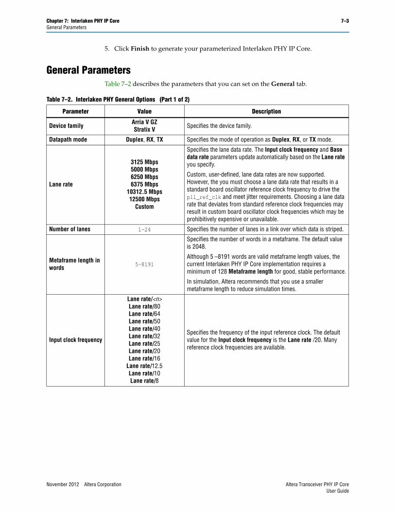
Chapter 7: Interlaken PHY IP Core 7–3General Parameters
5. Click Finish to generate your parameterized Interlaken PHY IP Core.
General ParametersTable 7–2 describes the parameters that you can set on the General tab.
Table 7–2. Interlaken PHY General Options (Part 1 of 2)
Parameter Value Description
Device family Arria V GZStratix V Specifies the device family.
Datapath mode Duplex, RX, TX Specifies the mode of operation as Duplex, RX, or TX mode.
Lane rate
3125 Mbps5000 Mbps6250 Mbps6375 Mbps
10312.5 Mbps12500 Mbps
Custom
Specifies the lane data rate. The Input clock frequency and Base data rate parameters update automatically based on the Lane rate you specify.
Custom, user-defined, lane data rates are now supported. However, the you must choose a lane data rate that results in a standard board oscillator reference clock frequency to drive the pll_ref_clk and meet jitter requirements. Choosing a lane data rate that deviates from standard reference clock frequencies may result in custom board oscillator clock frequencies which may be prohibitively expensive or unavailable.
Number of lanes 1–24 Specifies the number of lanes in a link over which data is striped.
Metaframe length in words 5–8191
Specifies the number of words in a metaframe. The default value is 2048.
Although 5 –8191 words are valid metaframe length values, the current Interlaken PHY IP Core implementation requires a minimum of 128 Metaframe length for good, stable performance.
In simulation, Altera recommends that you use a smaller metaframe length to reduce simulation times.
Input clock frequency
Lane rate/<n> Lane rate/80Lane rate/64Lane rate/50Lane rate/40Lane rate/32Lane rate/25Lane rate/20Lane rate/16
Lane rate/12.5Lane rate/10Lane rate/8
Specifies the frequency of the input reference clock. The default value for the Input clock frequency is the Lane rate /20. Many reference clock frequencies are available.
November 2012 Altera Corporation Altera Transceiver PHY IP CoreUser Guide
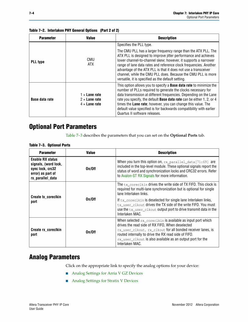
7–4 Chapter 7: Interlaken PHY IP CoreOptional Port Parameters
Optional Port ParametersTable 7–3 describes the parameters that you can set on the Optional Ports tab.
Analog ParametersClick on the appropriate link to specify the analog options for your device:
■ Analog Settings for Arria V GZ Devices
■ Analog Settings for Stratix V Devices
PLL type CMUATX
Specifies the PLL type.
The CMU PLL has a larger frequency range than the ATX PLL. The ATX PLL is designed to improve jitter performance and achieves lower channel-to-channel skew; however, it supports a narrower range of lane data rates and reference clock frequencies. Another advantage of the ATX PLL is that it does not use a transceiver channel, while the CMU PLL does. Because the CMU PLL is more versatile, it is specified as the default setting.
Base data rate1 × Lane rate2 × Lane rate4 × Lane rate
This option allows you to specify a Base data rate to minimize the number of PLLs required to generate the clocks necessary for data transmission at different frequencies. Depending on the Lane rate you specify, the default Base data rate can be either 1, 2, or 4 times the Lane rate; however, you can change this value. The default value specified is for backwards compatibility with earlier Quartus II software releases.
Table 7–2. Interlaken PHY General Options (Part 2 of 2)
Parameter Value Description
Table 7–3. Optional Ports
Parameter Value Description
Enable RX status signals, (word lock, sync lock, crc32 error) as part of rx_parallel_data
On/Off
When you turn this option on, rx_parallel_data[71:69] are included in the top-level module. These optional signals report the status of word and synchronization locks and CRC32 errors. Refer to Avalon-ST RX Signals for more information.
Create tx_coreclkin port On/Off
The tx_coreclkin drives the write side of TX FIFO. This clock is required for multi-lane synchronization but is optional for single lane Interlaken links.
If tx_coreclkin is deselected for single lane Interlaken links, tx_user_clkout drives the TX side of the write FIFO. You must use the tx_user_clkout output port to drive transmit data in the Interlaken MAC.
Create rx_coreclkin port On/Off
When selected rx_coreclkin is available as input port which drives the read side of RX FIFO, When deselected rx_user_clkout, rx_clkout for all bonded receiver lanes, is routed internally to drive the RX read side of FIFO. rx_user_clkout is also available as an output port for the Interlaken MAC.
Altera Transceiver PHY IP Core November 2012 Altera CorporationUser Guide
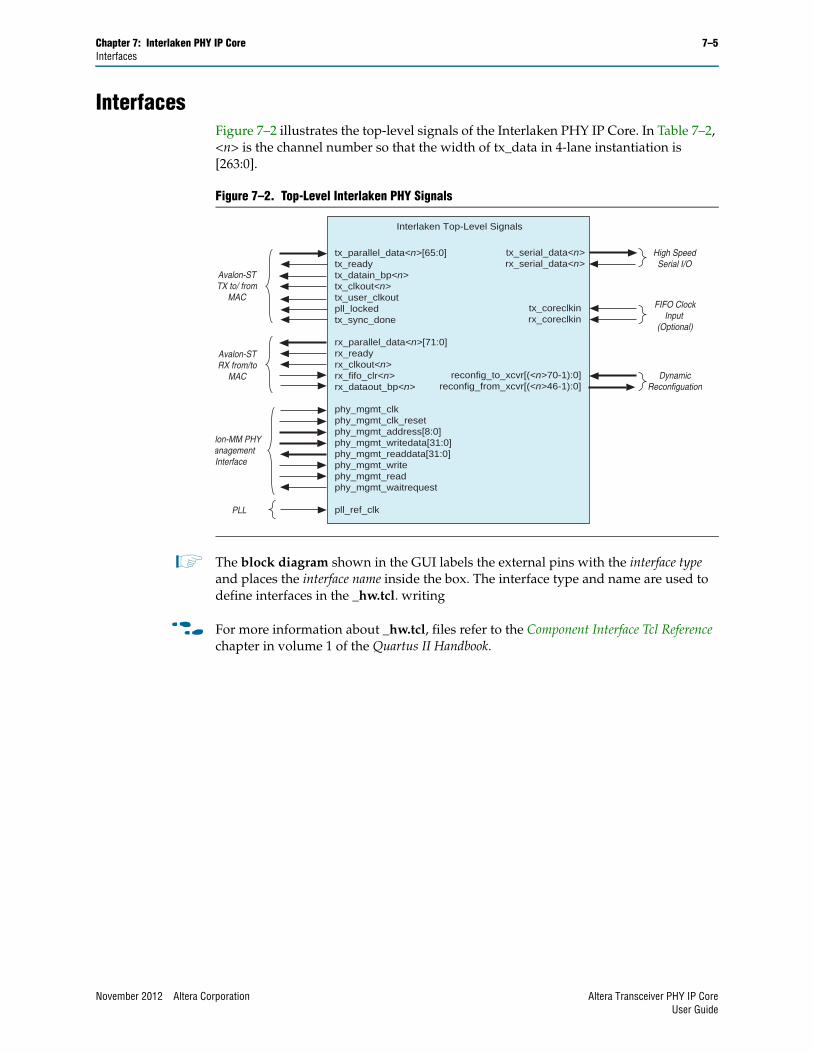
Chapter 7: Interlaken PHY IP Core 7–5Interfaces
InterfacesFigure 7–2 illustrates the top-level signals of the Interlaken PHY IP Core. In Table 7–2, <n> is the channel number so that the width of tx_data in 4-lane instantiation is [263:0].
1 The block diagram shown in the GUI labels the external pins with the interface type and places the interface name inside the box. The interface type and name are used to define interfaces in the _hw.tcl. writing
f For more information about _hw.tcl, files refer to the Component Interface Tcl Reference chapter in volume 1 of the Quartus II Handbook.
Figure 7–2. Top-Level Interlaken PHY Signals
tx_parallel_data<n>[65:0]tx_readytx_datain_bp<n>tx_clkout<n>tx_user_clkoutpll_lockedtx_sync_done
rx_parallel_data<n>[71:0]rx_readyrx_clkout<n>rx_fifo_clr<n>rx_dataout_bp<n>
phy_mgmt_clkphy_mgmt_clk_resetphy_mgmt_address[8:0]phy_mgmt_writedata[31:0]phy_mgmt_readdata[31:0]phy_mgmt_writephy_mgmt_readphy_mgmt_waitrequest
pll_ref_clk
Interlaken Top-Level Signals
tx_serial_data<n>rx_serial_data<n>
Avalon-STTX to/ from
MAC
High SpeedSerial I/O
PLL
alon-MM PHYanagementInterface
Avalon-STRX from/to
MAC DynamicReconfiguation
tx_coreclkinrx_coreclkin
reconfig_to_xcvr[(<n>70-1):0]reconfig_from_xcvr[(<n>46-1):0]
FIFO ClockInput
(Optional)
November 2012 Altera Corporation Altera Transceiver PHY IP CoreUser Guide
7–6 Chapter 7: Interlaken PHY IP CoreAvalon-ST TX Interface
Avalon-ST TX InterfaceTable 7–4 lists the signals in the Avalon-ST TX interface.
Table 7–4. Avalon-ST TX Signals (Part 1 of 3)
Signal Name Direction Description
tx_parallel_data<n>[63:0] Input Avalon-ST data bus driven from the FPGA fabric to the TX PCS. This input should be synchronized to the tx_coreclkin clock domain.
tx_parallel_data<n>[64] Input
Indicates whether tx_parallel_data<n>[63:0] represents control or data. When deasserted, tx_parallel_data<n>[63:0] is a data word. When asserted, tx_parallel_data<n>[63:0] is a control word.
The value of header synchronization bits[65:64] of the Interlaken word identify whether bits[63:0] are a Framing Layer Control/Burst/IDLE Control Word or a data word. The MAC must gray encode the header synchronization bits. The value 2’b10 indicating Burst/IDLE Control Word must be gray encoded to the value 1’b1 for tx_parallel_data<n>[64]. The value 2’b01 indicating data word must be gray encoded to the value 1’b0 for tx_parallel_data<n>[64]. You can also tie header synchronization bit[65] to tx_parallel_data[64] directly.
tx_parallel_data<n>[65] Input
When asserted, indicates that tx_parallel_data<n>[63:0] is valid and is ready to be written into the TX FIFO. When deasserted, indicates that tx_parallel_data<n>[63:0] is invalid and is not written into the TX FIFO. This signal is the data valid or write enable port of the TX FIFO. This input must be synchronized to the tx_coreclkin clock domain.
The Interlaken MAC should gate tx_parallel_data<n>[65] based on tx_datain_bp<n>. Or, you can tie tx_datain_bp<n> directly to tx_parallel_data<n>[65]. For Quartus II releases before 12.0, you must pre-fill the transmit FIFO so this pin must be 1’b1 when tx_ready is asserted, but before tx_sync_done is asserted to insert the pre-fill pattern. Do not use valid data to pre-fill the transmit FIFO. Use the following Verilog HDL assignment for Quartus II releases prior to 12.0:
assign tx_parallel_data[65] = (!tx_sync_done)?1'b1:tx_datain_bp[0];
Altera Transceiver PHY IP Core November 2012 Altera CorporationUser Guide
Chapter 7: Interlaken PHY IP Core 7–7Avalon-ST TX Interface
tx_ready Output
When asserted, indicates that the TX interface has exited the reset state and is ready for service. The tx_ready latency for the TX interface is 0. A 0 latency means that the TX FIFO can accept data on the same clock cycle that tx_ready is asserted. This output is synchronous to the phy_mgmt_clk clock domain. The Interlaken MAC must wait for tx_ready before initiating data transfer (pre-fill pattern or valid user data) on any lanes. The TX FIFO only captures input data from the Interlaken MAC when tx_ready and tx_parallel_data[65] are both asserted.
For Quartus versions earlier than 12.0, the user is a required to pre-fill the transmit FIFO. Do not use valid user data to pre-fill the transmit FIFO.
The beginning of the pre-fill stage is marked by the assertion of tx_ready, before tx_sync_done is asserted. The pre-fill stage should terminate when tx_ready is high and tx_sync_done changes from Logic 0 to Logic 1 state. At this point, TX synchronization is complete and valid TX data insertion can begin. TX synchronization is not required for single-lane variants. Use the following Verilog HDL assignment is for Quartus versions earlier than 12.0.
assign tx_parallel_data[65] = (!tx_sync_done)?1'b1:tx_datain_bp[0];
tx_datain_bp<n> Output
When asserted, indicates that Interlaken TX lane <n> interface is ready to receive data for transmission. In multi-lane configurations, the tx_datain_bp<n> signals must be logically Ored. The latency on this Avalon-ST interface is 0 cycles. The Interlaken MAC must only drive valid user data on tx_parallel_data<n>[64] and tx_parallel_data<n>[63:0] data bus as soon as tx_ready<n> and tx_sync_done are both asserted. The tx_datain_bp<n> signal is connected to the partial empty threshold of the TX FIFO, so that when tx_datain_bp<n> is deasserted the TX FIFO back pressures the Interlaken MAC. Stop sending TX data to the PHY when this signal is deasserted.
The Interlaken MAC can continue driving data to the TX FIFO when tx_datain_bp<n> is asserted. The Interlaken MAC should gate tx_parallel_data<n>[65], which operates as a data_valid signal, based on tx_datain_bp<n>. This output is synchronous to the tx_coreclkin clock domain. Or, you can also tie tx_datain_bp<n> directly to tx_parallel_data<n>[65]. For Quartus II releases prior to 12.0, you must pre-fill the TX FIFO before tx_sync_done can be asserted. Do not use valid data to pre-fill the TX FIFO. Use the following Verilog HDL assignment for Quartus II releases prior to 12.0:
assign tx_parallel_data[65] = (!tx_sync_done)?1'b1:tx_datain_bp[0];
tx_clkout Output Output clock from the TX PCS. The frequency of this clock equals the Lane rate divided by 40, which is the PMA serialization factor.
Table 7–4. Avalon-ST TX Signals (Part 2 of 3)
Signal Name Direction Description
November 2012 Altera Corporation Altera Transceiver PHY IP CoreUser Guide
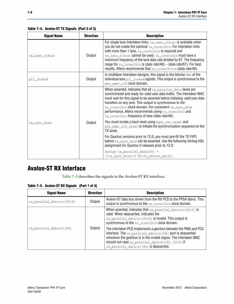
7–8 Chapter 7: Interlaken PHY IP CoreAvalon-ST RX Interface
Avalon-ST RX InterfaceTable 7–5 describes the signals in the Avalon-ST RX interface.
tx_user_clkout Output
For single lane Interlaken links, tx_user_clkout is available when you do not create the optional tx_coreclkin. For Interlaken links with more than 1 lane, tx_coreclkin is required and tx_user_clkout cannot be used. tx_coreclkin must have a minimum frequency of the lane data rate divided by 67. The frequency range for tx_coreclkin is (data rate/40) – (data rate/67). For best results, Altera recommends that rx_coreclkin = (data rate/40).
pll_locked OutputIn multilane Interlaken designs, this signal is the bitwise AND of the individual lane pll_locked signals. This output is synchronous to the phy_mgmt_clk clock domain.
tx_sync_done Output
When asserted, indicates that all tx_parallel_data lanes are synchronized and ready for valid user data traffic. The Interlaken MAC must wait for this signal to be asserted before initiating valid user data transfers on any lane. This output is synchronous to the tx_coreclkin clock domain. For consistent tx_sync_done performance, Altera recommends using tx_coreclkin and rx_coreclkin frequency of lane (data rate/40).
You must invoke a hard reset using mgmt_rst_reset and phy_mgmt_clk_reset to initiate the synchronization sequence on the TX lanes.
For Quartus versions prior to 12.0, you must pre-fill the TX FIFO before tx_sync_done can be asserted. Use the following Verilog HDL assignment for Quartus II releases prior to 12.0:
assign tx_parallel_data[65] = (!tx_sync_done)?1'b1:tx_datain_bp[0];
Table 7–4. Avalon-ST TX Signals (Part 3 of 3)
Signal Name Direction Description
Table 7–5. Avalon-ST RX Signals (Part 1 of 4)
Signal Name Direction Description
rx_parallel_data<n>[63:0] Output Avalon-ST data bus driven from the RX PCS to the FPGA fabric. This output is synchronous to the rx_coreclkin clock domain.
rx_parallel_data<n>[64] Output
When asserted, indicates that rx_parallel_data<n>[63:0] is valid. When deasserted, indicates the rx_parallel_data<n>[63:0] is invalid. This output is synchronous to the rx_coreclkin clock domain.
The Interlaken PCS implements a gearbox between the PMA and PCS interface. The rx_parallel_data<n>[64] port is deasserted whenever the gearbox is in the invalid region. The Interlaken MAC should not read rx_parallel_data<n>[65, 63:0] if rx_parallel_data<n>[64] is deasserted.
Altera Transceiver PHY IP Core November 2012 Altera CorporationUser Guide
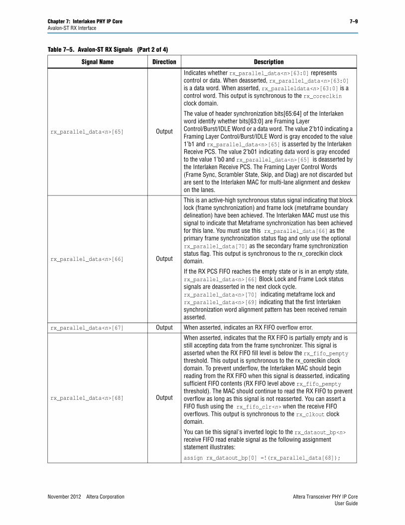
Chapter 7: Interlaken PHY IP Core 7–9Avalon-ST RX Interface
rx_parallel_data<n>[65] Output
Indicates whether rx_parallel_data<n>[63:0] represents control or data. When deasserted, rx_parallel_data<n>[63:0] is a data word. When asserted, rx_paralleldata<n>[63:0] is a control word. This output is synchronous to the rx_coreclkin clock domain.
The value of header synchronization bits[65:64] of the Interlaken word identify whether bits[63:0] are Framing Layer Control/Burst/IDLE Word or a data word. The value 2’b10 indicating a Framing Layer Control/Burst/IDLE Word is gray encoded to the value 1’b1 and rx_parallel_data<n>[65] is asserted by the Interlaken Receive PCS. The value 2’b01 indicating data word is gray encoded to the value 1’b0 and rx_parallel_data<n>[65] is deasserted by the Interlaken Receive PCS. The Framing Layer Control Words (Frame Sync, Scrambler State, Skip, and Diag) are not discarded but are sent to the Interlaken MAC for multi-lane alignment and deskew on the lanes.
rx_parallel_data<n>[66] Output
This is an active-high synchronous status signal indicating that block lock (frame synchronization) and frame lock (metaframe boundary delineation) have been achieved. The Interlaken MAC must use this signal to indicate that Metaframe synchronization has been achieved for this lane. You must use this rx_parallel_data[66] as the primary frame synchronization status flag and only use the optional rx_parallel_data[70] as the secondary frame synchronization status flag. This output is synchronous to the rx_coreclkin clock domain.
If the RX PCS FIFO reaches the empty state or is in an empty state, rx_parallel_data<n>[66] Block Lock and Frame Lock status signals are deasserted in the next clock cycle. rx_parallel_data<n>[70] indicating metaframe lock and rx_parallel_data<n>[69] indicating that the first Interlaken synchronization word alignment pattern has been received remain asserted.
rx_parallel_data<n>[67] Output When asserted, indicates an RX FIFO overflow error.
rx_parallel_data<n>[68] Output
When asserted, indicates that the RX FIFO is partially empty and is still accepting data from the frame synchronizer. This signal is asserted when the RX FIFO fill level is below the rx_fifo_pempty threshold. This output is synchronous to the rx_coreclkin clock domain. To prevent underflow, the Interlaken MAC should begin reading from the RX FIFO when this signal is deasserted, indicating sufficient FIFO contents (RX FIFO level above rx_fifo_pempty threshold). The MAC should continue to read the RX FIFO to prevent overflow as long as this signal is not reasserted. You can assert a FIFO flush using the rx_fifo_clr<n> when the receive FIFO overflows. This output is synchronous to the rx_clkout clock domain.
You can tie this signal's inverted logic to the rx_dataout_bp<n> receive FIFO read enable signal as the following assignment statement illustrates:
assign rx_dataout_bp[0] =!(rx_parallel_data[68]);
Table 7–5. Avalon-ST RX Signals (Part 2 of 4)
Signal Name Direction Description
November 2012 Altera Corporation Altera Transceiver PHY IP CoreUser Guide
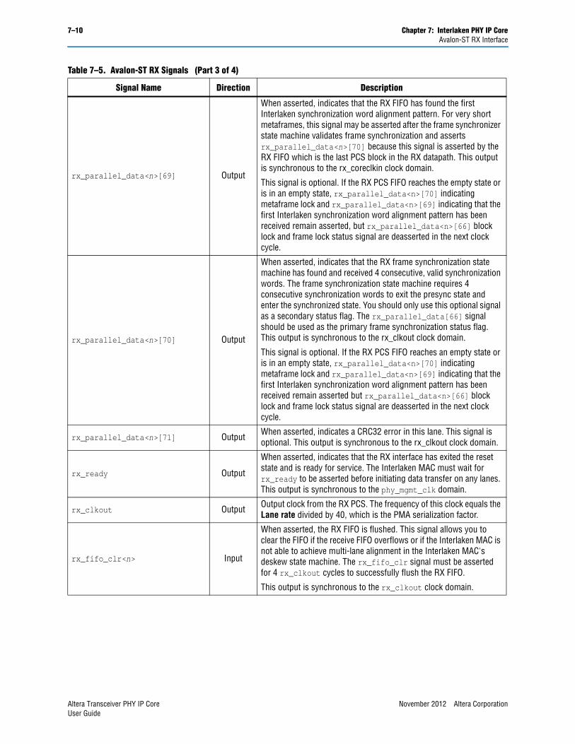
7–10 Chapter 7: Interlaken PHY IP CoreAvalon-ST RX Interface
rx_parallel_data<n>[69] Output
When asserted, indicates that the RX FIFO has found the first Interlaken synchronization word alignment pattern. For very short metaframes, this signal may be asserted after the frame synchronizer state machine validates frame synchronization and asserts rx_parallel_data<n>[70] because this signal is asserted by the RX FIFO which is the last PCS block in the RX datapath. This output is synchronous to the rx_coreclkin clock domain.
This signal is optional. If the RX PCS FIFO reaches the empty state or is in an empty state, rx_parallel_data<n>[70] indicating metaframe lock and rx_parallel_data<n>[69] indicating that the first Interlaken synchronization word alignment pattern has been received remain asserted, but rx_parallel_data<n>[66] block lock and frame lock status signal are deasserted in the next clock cycle.
rx_parallel_data<n>[70] Output
When asserted, indicates that the RX frame synchronization state machine has found and received 4 consecutive, valid synchronization words. The frame synchronization state machine requires 4 consecutive synchronization words to exit the presync state and enter the synchronized state. You should only use this optional signal as a secondary status flag. The rx_parallel_data[66] signal should be used as the primary frame synchronization status flag. This output is synchronous to the rx_clkout clock domain.
This signal is optional. If the RX PCS FIFO reaches an empty state or is in an empty state, rx_parallel_data<n>[70] indicating metaframe lock and rx_parallel_data<n>[69] indicating that the first Interlaken synchronization word alignment pattern has been received remain asserted but rx_parallel_data<n>[66] block lock and frame lock status signal are deasserted in the next clock cycle.
rx_parallel_data<n>[71] Output When asserted, indicates a CRC32 error in this lane. This signal is optional. This output is synchronous to the rx_clkout clock domain.
rx_ready Output
When asserted, indicates that the RX interface has exited the reset state and is ready for service. The Interlaken MAC must wait for rx_ready to be asserted before initiating data transfer on any lanes. This output is synchronous to the phy_mgmt_clk domain.
rx_clkout Output Output clock from the RX PCS. The frequency of this clock equals the Lane rate divided by 40, which is the PMA serialization factor.
rx_fifo_clr<n> Input
When asserted, the RX FIFO is flushed. This signal allows you to clear the FIFO if the receive FIFO overflows or if the Interlaken MAC is not able to achieve multi-lane alignment in the Interlaken MAC's deskew state machine. The rx_fifo_clr signal must be asserted for 4 rx_clkout cycles to successfully flush the RX FIFO.
This output is synchronous to the rx_clkout clock domain.
Table 7–5. Avalon-ST RX Signals (Part 3 of 4)
Signal Name Direction Description
Altera Transceiver PHY IP Core November 2012 Altera CorporationUser Guide
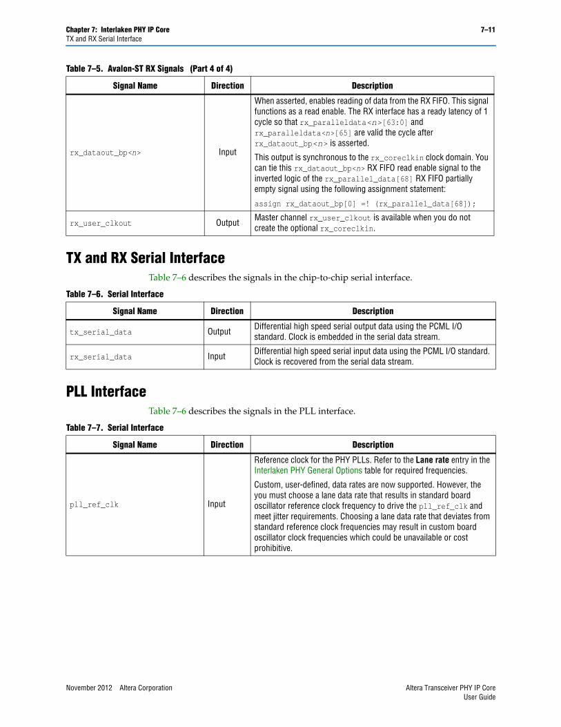
Chapter 7: Interlaken PHY IP Core 7–11TX and RX Serial Interface
TX and RX Serial InterfaceTable 7–6 describes the signals in the chip-to-chip serial interface.
PLL InterfaceTable 7–6 describes the signals in the PLL interface.
rx_dataout_bp<n> Input
When asserted, enables reading of data from the RX FIFO. This signal functions as a read enable. The RX interface has a ready latency of 1 cycle so that rx_paralleldata<n>[63:0] and rx_paralleldata<n>[65] are valid the cycle after rx_dataout_bp<n> is asserted.
This output is synchronous to the rx_coreclkin clock domain. You can tie this rx_dataout_bp<n> RX FIFO read enable signal to the inverted logic of the rx_parallel_data[68] RX FIFO partially empty signal using the following assignment statement:
assign rx_dataout_bp[0] =! (rx_parallel_data[68]);
rx_user_clkout Output Master channel rx_user_clkout is available when you do not create the optional rx_coreclkin.
Table 7–5. Avalon-ST RX Signals (Part 4 of 4)
Signal Name Direction Description
Table 7–6. Serial Interface
Signal Name Direction Description
tx_serial_data Output Differential high speed serial output data using the PCML I/O standard. Clock is embedded in the serial data stream.
rx_serial_data Input Differential high speed serial input data using the PCML I/O standard. Clock is recovered from the serial data stream.
Table 7–7. Serial Interface
Signal Name Direction Description
pll_ref_clk Input
Reference clock for the PHY PLLs. Refer to the Lane rate entry in the Interlaken PHY General Options table for required frequencies.
Custom, user-defined, data rates are now supported. However, the you must choose a lane data rate that results in standard board oscillator reference clock frequency to drive the pll_ref_clk and meet jitter requirements. Choosing a lane data rate that deviates from standard reference clock frequencies may result in custom board oscillator clock frequencies which could be unavailable or cost prohibitive.
November 2012 Altera Corporation Altera Transceiver PHY IP CoreUser Guide
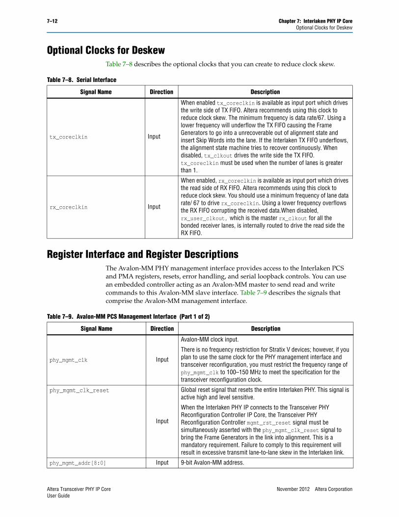
7–12 Chapter 7: Interlaken PHY IP CoreOptional Clocks for Deskew
Optional Clocks for DeskewTable 7–8 describes the optional clocks that you can create to reduce clock skew.
Register Interface and Register DescriptionsThe Avalon-MM PHY management interface provides access to the Interlaken PCS and PMA registers, resets, error handling, and serial loopback controls. You can use an embedded controller acting as an Avalon-MM master to send read and write commands to this Avalon-MM slave interface. Table 7–9 describes the signals that comprise the Avalon-MM management interface.
Table 7–8. Serial Interface
Signal Name Direction Description
tx_coreclkin Input
When enabled tx_coreclkin is available as input port which drives the write side of TX FIFO. Altera recommends using this clock to reduce clock skew. The minimum frequency is data rate/67. Using a lower frequency will underflow the TX FIFO causing the Frame Generators to go into a unrecoverable out of alignment state and insert Skip Words into the lane. If the Interlaken TX FIFO underflows, the alignment state machine tries to recover continuously. When disabled, tx_clkout drives the write side the TX FIFO. tx_coreclkin must be used when the number of lanes is greater than 1.
rx_coreclkin Input
When enabled, rx_coreclkin is available as input port which drives the read side of RX FIFO. Altera recommends using this clock to reduce clock skew. You should use a minimum frequency of lane data rate/ 67 to drive rx_coreclkin. Using a lower frequency overflows the RX FIFO corrupting the received data.When disabled, rx_user_clkout, which is the master rx_clkout for all the bonded receiver lanes, is internally routed to drive the read side the RX FIFO.
Table 7–9. Avalon-MM PCS Management Interface (Part 1 of 2)
Signal Name Direction Description
phy_mgmt_clk Input
Avalon-MM clock input.
There is no frequency restriction for Stratix V devices; however, if you plan to use the same clock for the PHY management interface and transceiver reconfiguration, you must restrict the frequency range of phy_mgmt_clk to 100–150 MHz to meet the specification for the transceiver reconfiguration clock.
phy_mgmt_clk_reset
Input
Global reset signal that resets the entire Interlaken PHY. This signal is active high and level sensitive.
When the Interlaken PHY IP connects to the Transceiver PHY Reconfiguration Controller IP Core, the Transceiver PHY Reconfiguration Controller mgmt_rst_reset signal must be simultaneously asserted with the phy_mgmt_clk_reset signal to bring the Frame Generators in the link into alignment. This is a mandatory requirement. Failure to comply to this requirement will result in excessive transmit lane-to-lane skew in the Interlaken link.
phy_mgmt_addr[8:0] Input 9-bit Avalon-MM address.
Altera Transceiver PHY IP Core November 2012 Altera CorporationUser Guide
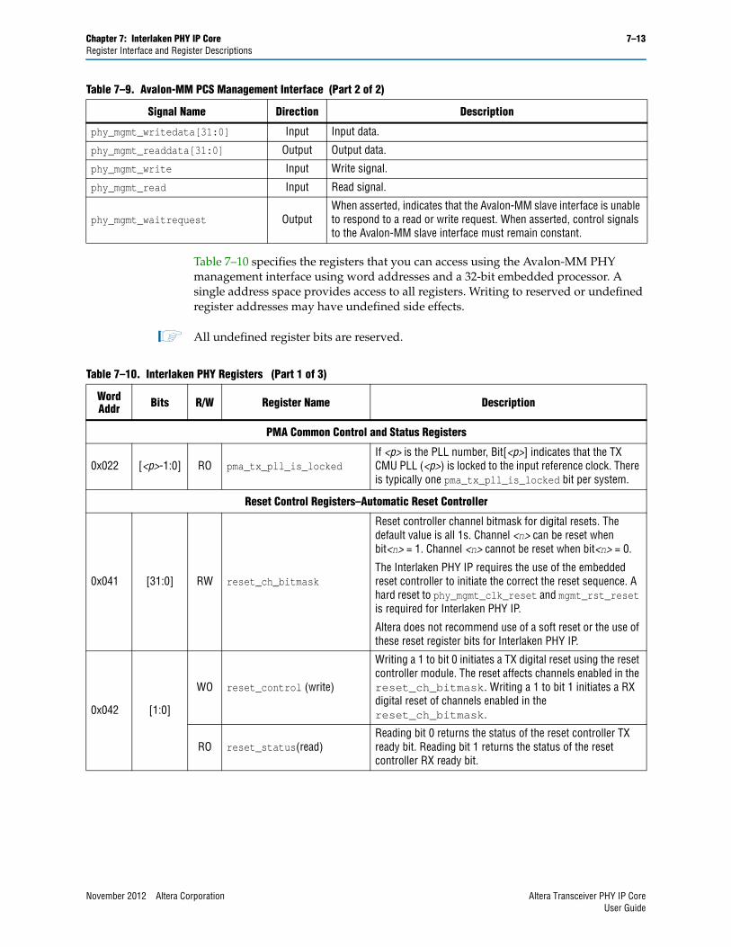
Chapter 7: Interlaken PHY IP Core 7–13Register Interface and Register Descriptions
Table 7–10 specifies the registers that you can access using the Avalon-MM PHY management interface using word addresses and a 32-bit embedded processor. A single address space provides access to all registers. Writing to reserved or undefined register addresses may have undefined side effects.
1 All undefined register bits are reserved.
phy_mgmt_writedata[31:0] Input Input data.
phy_mgmt_readdata[31:0] Output Output data.
phy_mgmt_write Input Write signal.
phy_mgmt_read Input Read signal.
phy_mgmt_waitrequest OutputWhen asserted, indicates that the Avalon-MM slave interface is unable to respond to a read or write request. When asserted, control signals to the Avalon-MM slave interface must remain constant.
Table 7–9. Avalon-MM PCS Management Interface (Part 2 of 2)
Signal Name Direction Description
Table 7–10. Interlaken PHY Registers (Part 1 of 3)
Word Addr Bits R/W Register Name Description
PMA Common Control and Status Registers
0x022 [<p>-1:0] RO pma_tx_pll_is_lockedIf <p> is the PLL number, Bit[<p>] indicates that the TX CMU PLL (<p>) is locked to the input reference clock. There is typically one pma_tx_pll_is_locked bit per system.
Reset Control Registers–Automatic Reset Controller
0x041 [31:0] RW reset_ch_bitmask
Reset controller channel bitmask for digital resets. The default value is all 1s. Channel <n> can be reset when bit<n> = 1. Channel <n> cannot be reset when bit<n> = 0.
The Interlaken PHY IP requires the use of the embedded reset controller to initiate the correct the reset sequence. A hard reset to phy_mgmt_clk_reset and mgmt_rst_reset is required for Interlaken PHY IP.
Altera does not recommend use of a soft reset or the use of these reset register bits for Interlaken PHY IP.
0x042 [1:0]
WO reset_control (write)
Writing a 1 to bit 0 initiates a TX digital reset using the reset controller module. The reset affects channels enabled in the reset_ch_bitmask. Writing a 1 to bit 1 initiates a RX digital reset of channels enabled in the reset_ch_bitmask.
RO reset_status(read)Reading bit 0 returns the status of the reset controller TX ready bit. Reading bit 1 returns the status of the reset controller RX ready bit.
November 2012 Altera Corporation Altera Transceiver PHY IP CoreUser Guide
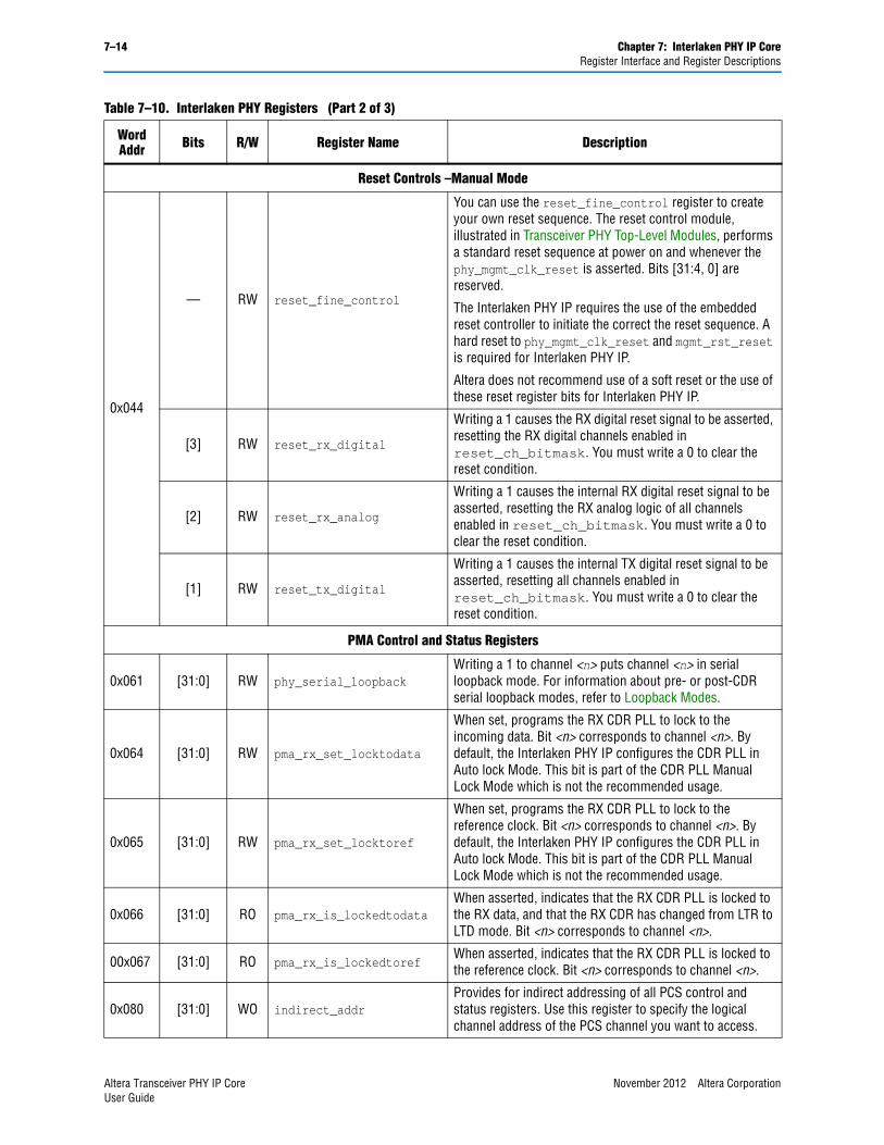
7–14 Chapter 7: Interlaken PHY IP CoreRegister Interface and Register Descriptions
Reset Controls –Manual Mode
0x044
— RW reset_fine_control
You can use the reset_fine_control register to create your own reset sequence. The reset control module, illustrated in Transceiver PHY Top-Level Modules, performs a standard reset sequence at power on and whenever the phy_mgmt_clk_reset is asserted. Bits [31:4, 0] are reserved.
The Interlaken PHY IP requires the use of the embedded reset controller to initiate the correct the reset sequence. A hard reset to phy_mgmt_clk_reset and mgmt_rst_reset is required for Interlaken PHY IP.
Altera does not recommend use of a soft reset or the use of these reset register bits for Interlaken PHY IP.
[3] RW reset_rx_digital
Writing a 1 causes the RX digital reset signal to be asserted, resetting the RX digital channels enabled in reset_ch_bitmask. You must write a 0 to clear the reset condition.
[2] RW reset_rx_analog
Writing a 1 causes the internal RX digital reset signal to be asserted, resetting the RX analog logic of all channels enabled in reset_ch_bitmask. You must write a 0 to clear the reset condition.
[1] RW reset_tx_digital
Writing a 1 causes the internal TX digital reset signal to be asserted, resetting all channels enabled in reset_ch_bitmask. You must write a 0 to clear the reset condition.
PMA Control and Status Registers
0x061 [31:0] RW phy_serial_loopbackWriting a 1 to channel <n> puts channel <n> in serial loopback mode. For information about pre- or post-CDR serial loopback modes, refer to Loopback Modes.
0x064 [31:0] RW pma_rx_set_locktodata
When set, programs the RX CDR PLL to lock to the incoming data. Bit <n> corresponds to channel <n>. By default, the Interlaken PHY IP configures the CDR PLL in Auto lock Mode. This bit is part of the CDR PLL Manual Lock Mode which is not the recommended usage.
0x065 [31:0] RW pma_rx_set_locktoref
When set, programs the RX CDR PLL to lock to the reference clock. Bit <n> corresponds to channel <n>. By default, the Interlaken PHY IP configures the CDR PLL in Auto lock Mode. This bit is part of the CDR PLL Manual Lock Mode which is not the recommended usage.
0x066 [31:0] RO pma_rx_is_lockedtodataWhen asserted, indicates that the RX CDR PLL is locked to the RX data, and that the RX CDR has changed from LTR to LTD mode. Bit <n> corresponds to channel <n>.
00x067 [31:0] RO pma_rx_is_lockedtorefWhen asserted, indicates that the RX CDR PLL is locked to the reference clock. Bit <n> corresponds to channel <n>.
0x080 [31:0] WO indirect_addrProvides for indirect addressing of all PCS control and status registers. Use this register to specify the logical channel address of the PCS channel you want to access.
Table 7–10. Interlaken PHY Registers (Part 2 of 3)
Word Addr Bits R/W Register Name Description
Altera Transceiver PHY IP Core November 2012 Altera CorporationUser Guide
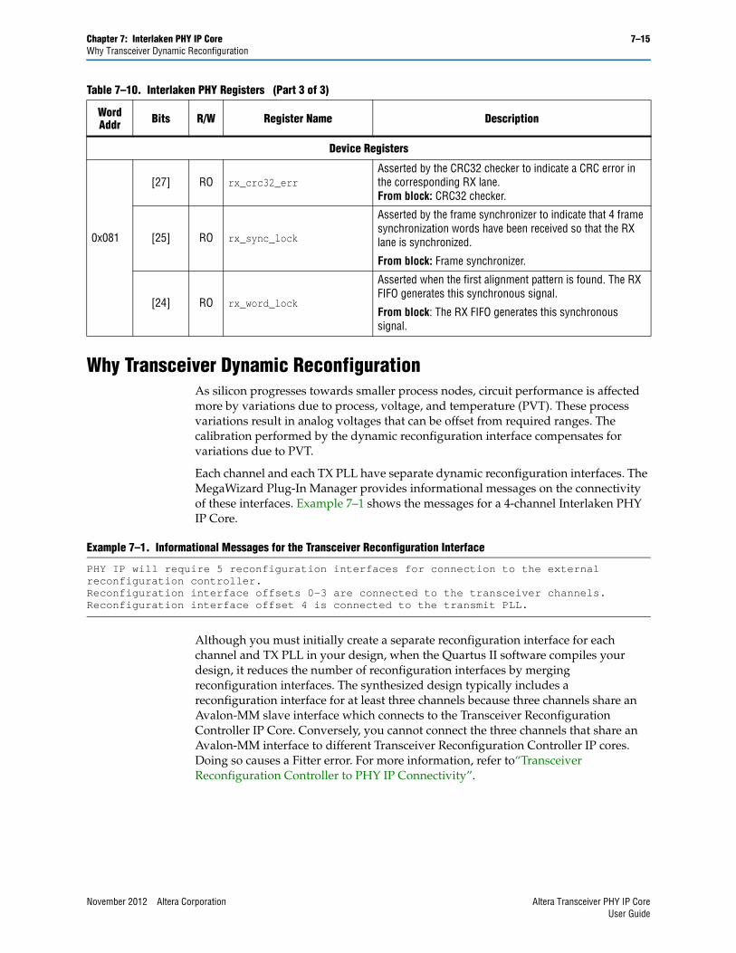
Chapter 7: Interlaken PHY IP Core 7–15Why Transceiver Dynamic Reconfiguration
Why Transceiver Dynamic ReconfigurationAs silicon progresses towards smaller process nodes, circuit performance is affected more by variations due to process, voltage, and temperature (PVT). These process variations result in analog voltages that can be offset from required ranges. The calibration performed by the dynamic reconfiguration interface compensates for variations due to PVT.
Each channel and each TX PLL have separate dynamic reconfiguration interfaces. The MegaWizard Plug-In Manager provides informational messages on the connectivity of these interfaces. Example 7–1 shows the messages for a 4-channel Interlaken PHY IP Core.
Although you must initially create a separate reconfiguration interface for each channel and TX PLL in your design, when the Quartus II software compiles your design, it reduces the number of reconfiguration interfaces by merging reconfiguration interfaces. The synthesized design typically includes a reconfiguration interface for at least three channels because three channels share an Avalon-MM slave interface which connects to the Transceiver Reconfiguration Controller IP Core. Conversely, you cannot connect the three channels that share an Avalon-MM interface to different Transceiver Reconfiguration Controller IP cores. Doing so causes a Fitter error. For more information, refer to“Transceiver Reconfiguration Controller to PHY IP Connectivity”.
Device Registers
[27] RO rx_crc32_errAsserted by the CRC32 checker to indicate a CRC error in the corresponding RX lane.From block: CRC32 checker.
0x081 [25] RO rx_sync_lock
Asserted by the frame synchronizer to indicate that 4 frame synchronization words have been received so that the RX lane is synchronized.
From block: Frame synchronizer.
[24] RO rx_word_lock
Asserted when the first alignment pattern is found. The RX FIFO generates this synchronous signal.
From block: The RX FIFO generates this synchronous signal.
Table 7–10. Interlaken PHY Registers (Part 3 of 3)
Word Addr Bits R/W Register Name Description
Example 7–1. Informational Messages for the Transceiver Reconfiguration Interface
PHY IP will require 5 reconfiguration interfaces for connection to the external reconfiguration controller.Reconfiguration interface offsets 0-3 are connected to the transceiver channels.Reconfiguration interface offset 4 is connected to the transmit PLL.
November 2012 Altera Corporation Altera Transceiver PHY IP CoreUser Guide
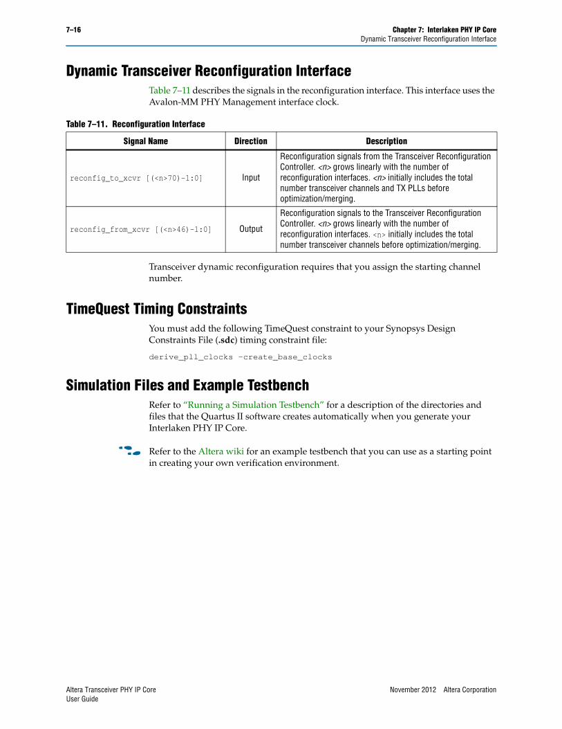
7–16 Chapter 7: Interlaken PHY IP CoreDynamic Transceiver Reconfiguration Interface
Dynamic Transceiver Reconfiguration InterfaceTable 7–11 describes the signals in the reconfiguration interface. This interface uses the Avalon-MM PHY Management interface clock.
Transceiver dynamic reconfiguration requires that you assign the starting channel number.
TimeQuest Timing ConstraintsYou must add the following TimeQuest constraint to your Synopsys Design Constraints File (.sdc) timing constraint file:
derive_pll_clocks -create_base_clocks
Simulation Files and Example Testbench Refer to “Running a Simulation Testbench” for a description of the directories and files that the Quartus II software creates automatically when you generate your Interlaken PHY IP Core.
f Refer to the Altera wiki for an example testbench that you can use as a starting point in creating your own verification environment.
Table 7–11. Reconfiguration Interface
Signal Name Direction Description
reconfig_to_xcvr [(<n>70)-1:0] Input
Reconfiguration signals from the Transceiver Reconfiguration Controller. <n> grows linearly with the number of reconfiguration interfaces. <n> initially includes the total number transceiver channels and TX PLLs before optimization/merging.
reconfig_from_xcvr [(<n>46)-1:0] Output
Reconfiguration signals to the Transceiver Reconfiguration Controller. <n> grows linearly with the number of reconfiguration interfaces. <n> initially includes the total number transceiver channels before optimization/merging.
Altera Transceiver PHY IP Core November 2012 Altera CorporationUser Guide
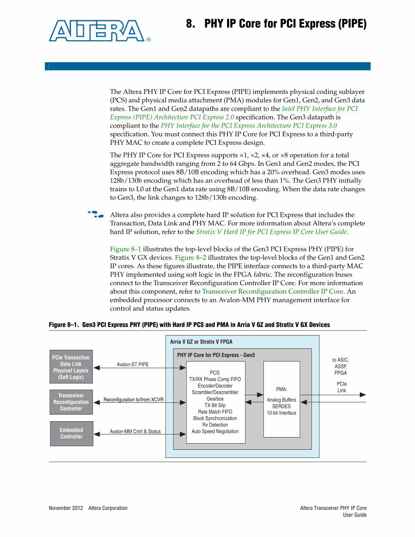
November 2012 Altera Corporation
8. PHY IP Core for PCI Express (PIPE)
The Altera PHY IP Core for PCI Express (PIPE) implements physical coding sublayer (PCS) and physical media attachment (PMA) modules for Gen1, Gen2, and Gen3 data rates. The Gen1 and Gen2 datapaths are compliant to the Intel PHY Interface for PCI Express (PIPE) Architecture PCI Express 2.0 specification. The Gen3 datapath is compliant to the PHY Interface for the PCI Express Architecture PCI Express 3.0 specification. You must connect this PHY IP Core for PCI Express to a third-party PHY MAC to create a complete PCI Express design.
The PHY IP Core for PCI Express supports ×1, ×2, ×4, or ×8 operation for a total aggregate bandwidth ranging from 2 to 64 Gbps. In Gen1 and Gen2 modes, the PCI Express protocol uses 8B/10B encoding which has a 20% overhead. Gen3 modes uses 128b/130b encoding which has an overhead of less than 1%. The Gen3 PHY initially trains to L0 at the Gen1 data rate using 8B/10B encoding. When the data rate changes to Gen3, the link changes to 128b/130b encoding.
f Altera also provides a complete hard IP solution for PCI Express that includes the Transaction, Data Link and PHY MAC. For more information about Altera’s complete hard IP solution, refer to the Stratix V Hard IP for PCI Express IP Core User Guide.
Figure 8–1 illustrates the top-level blocks of the Gen3 PCI Express PHY (PIPE) for Stratix V GX devices. Figure 8–2 illustrates the top-level blocks of the Gen1 and Gen2 IP cores. As these figures illustrate, the PIPE interface connects to a third-party MAC PHY implemented using soft logic in the FPGA fabric. The reconfiguration buses connect to the Transceiver Reconfiguration Controller IP Core. For more information about this component, refer to Transceiver Reconfiguration Controller IP Core. An embedded processor connects to an Avalon-MM PHY management interface for control and status updates.
Figure 8–1. Gen3 PCI Express PHY (PIPE) with Hard IP PCS and PMA in Arria V GZ and Stratix V GX Devices
PHY IP Core for PCI Express - Gen3
Arria V GZ or Stratix V FPGA
PMA:
Analog BuffersSERDES
10-bit Interface
Avalon-MM Cntrl & Status
Avalon-ST PIPEto ASIC,ASSP,FPGA
PCIeLink
TransceiverReconfiguration
Controller
EmbeddedController
PCIe TransactionData Link
Physical Layers(Soft Logic)
Reconfiguration to/from XCVR
PCS:TX/RX Phase Comp FIFO
Encoder/DecoderScrambler/Descrambler
GearboxTX Bit Slip
Rate Match FIFOBlock Synchronization
Rx DetectionAuto Speed Negotiation
Altera Transceiver PHY IP CoreUser Guide
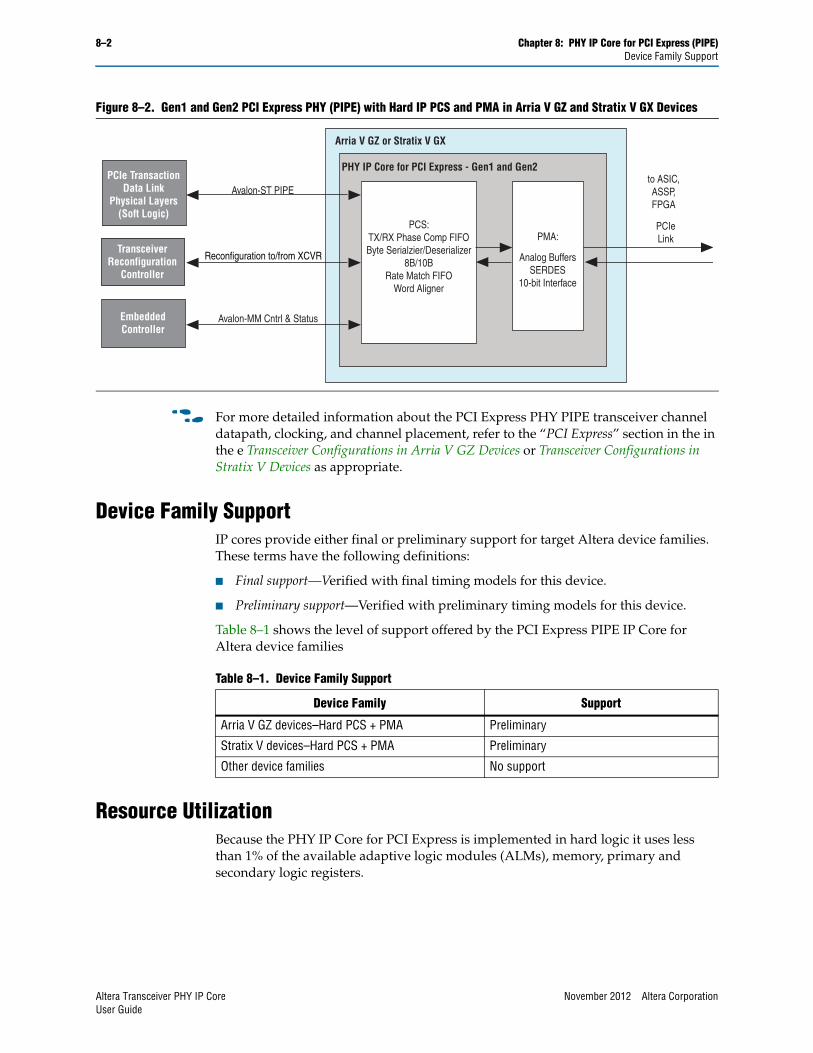
8–2 Chapter 8: PHY IP Core for PCI Express (PIPE)Device Family Support
f For more detailed information about the PCI Express PHY PIPE transceiver channel datapath, clocking, and channel placement, refer to the “PCI Express” section in the in the e Transceiver Configurations in Arria V GZ Devices or Transceiver Configurations in Stratix V Devices as appropriate.
Device Family SupportIP cores provide either final or preliminary support for target Altera device families. These terms have the following definitions:
■ Final support—Verified with final timing models for this device.
■ Preliminary support—Verified with preliminary timing models for this device.
Table 8–1 shows the level of support offered by the PCI Express PIPE IP Core for Altera device families
Resource Utilization Because the PHY IP Core for PCI Express is implemented in hard logic it uses less than 1% of the available adaptive logic modules (ALMs), memory, primary and secondary logic registers.
Figure 8–2. Gen1 and Gen2 PCI Express PHY (PIPE) with Hard IP PCS and PMA in Arria V GZ and Stratix V GX Devices
PHY IP Core for PCI Express - Gen1 and Gen2
Arria V GZ or Stratix V GX
PCS:TX/RX Phase Comp FIFOByte Serialzier/Deserializer
8B/10BRate Match FIFO
Word Aligner
PMA:
Analog BuffersSERDES
10-bit Interface
Avalon-MM Cntrl & Status
Avalon-ST PIPEto ASIC,ASSP,FPGA
PCIeLink
TransceiverReconfiguration
Controller
EmbeddedController
Reconfiguration to/from XCVR
PCIe TransactionData Link
Physical Layers(Soft Logic)
Table 8–1. Device Family Support
Device Family Support
Arria V GZ devices–Hard PCS + PMA Preliminary
Stratix V devices–Hard PCS + PMA Preliminary
Other device families No support
Altera Transceiver PHY IP Core November 2012 Altera CorporationUser Guide
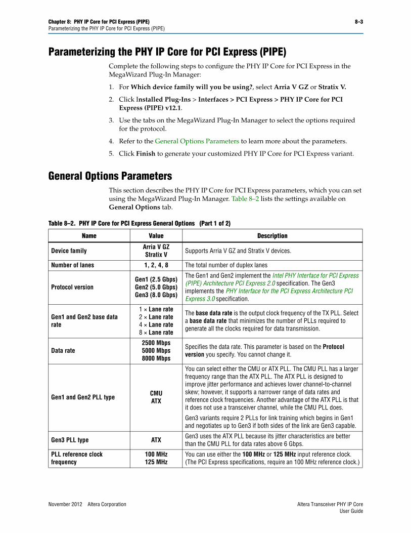
Chapter 8: PHY IP Core for PCI Express (PIPE) 8–3Parameterizing the PHY IP Core for PCI Express (PIPE)
Parameterizing the PHY IP Core for PCI Express (PIPE)Complete the following steps to configure the PHY IP Core for PCI Express in the MegaWizard Plug-In Manager:
1. For Which device family will you be using?, select Arria V GZ or Stratix V.
2. Click Installed Plug-Ins > Interfaces > PCI Express > PHY IP Core for PCI Express (PIPE) v12.1.
3. Use the tabs on the MegaWizard Plug-In Manager to select the options required for the protocol.
4. Refer to the General Options Parameters to learn more about the parameters.
5. Click Finish to generate your customized PHY IP Core for PCI Express variant.
General Options ParametersThis section describes the PHY IP Core for PCI Express parameters, which you can set using the MegaWizard Plug-In Manager. Table 8–2 lists the settings available on General Options tab.
Table 8–2. PHY IP Core for PCI Express General Options (Part 1 of 2)
Name Value Description
Device family Arria V GZStratix V Supports Arria V GZ and Stratix V devices.
Number of lanes 1, 2, 4, 8 The total number of duplex lanes
Protocol versionGen1 (2.5 Gbps)Gen2 (5.0 Gbps)Gen3 (8.0 Gbps)
The Gen1 and Gen2 implement the Intel PHY Interface for PCI Express (PIPE) Architecture PCI Express 2.0 specification. The Gen3 implements the PHY Interface for the PCI Express Architecture PCI Express 3.0 specification.
Gen1 and Gen2 base data rate
1 × Lane rate2 × Lane rate4 × Lane rate8 × Lane rate
The base data rate is the output clock frequency of the TX PLL. Select a base data rate that minimizes the number of PLLs required to generate all the clocks required for data transmission.
Data rate2500 Mbps5000 Mbps 8000 Mbps
Specifies the data rate. This parameter is based on the Protocol version you specify. You cannot change it.
Gen1 and Gen2 PLL type CMUATX
You can select either the CMU or ATX PLL. The CMU PLL has a larger frequency range than the ATX PLL. The ATX PLL is designed to improve jitter performance and achieves lower channel-to-channel skew; however, it supports a narrower range of data rates and reference clock frequencies. Another advantage of the ATX PLL is that it does not use a transceiver channel, while the CMU PLL does.
Gen3 variants require 2 PLLs for link training which begins in Gen1 and negotiates up to Gen3 if both sides of the link are Gen3 capable.
Gen3 PLL type ATX Gen3 uses the ATX PLL because its jitter characteristics are better than the CMU PLL for data rates above 6 Gbps.
PLL reference clock frequency
100 MHz125 MHz
You can use either the 100 MHz or 125 MHz input reference clock. (The PCI Express specifications, require an 100 MHz reference clock.)
November 2012 Altera Corporation Altera Transceiver PHY IP CoreUser Guide
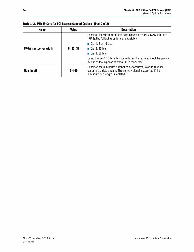
8–4 Chapter 8: PHY IP Core for PCI Express (PIPE)General Options Parameters
FPGA transceiver width 8, 16, 32
Specifies the width of the interface between the PHY MAC and PHY (PIPE).The following options are available:
■ Gen1: 8 or 16 bits
■ Gen2: 16 bits
■ Gen3: 32 bits
Using the Gen1 16-bit interface reduces the required clock frequency by half at the expense of extra FPGA resources.
Run length 5–160Specifies the maximum number of consecutive 0s or 1s that can occur in the data stream. The rx_rlv signal is asserted if the maximum run length is violated.
Table 8–2. PHY IP Core for PCI Express General Options (Part 2 of 2)
Name Value Description
Altera Transceiver PHY IP Core November 2012 Altera CorporationUser Guide

Chapter 8: PHY IP Core for PCI Express (PIPE) 8–5Interfaces
InterfacesThis section describes interfaces of the PHY IP Core for PCI Express (PIPE). It includes Figure 8–3 illustrates the top-level pinout of the PHY IP Core for PCI Express PHY. The port descriptions use the following variables to represent parameters:
■ <n>—The number of lanes
■ <d>—The total deserialization factor from the input pin to the PHY MAC interface.
■ <s>—The symbols size.
■ <r>—The width of the reconfiguration interface; <r> is automatically calculated based on the selected configuration
1 The block diagram shown in the GUI labels the external pins with the interface type and places the interface name inside the box. The interface type and name are used in the _hw.tcl file. If you turn on Show signals, the block diagram displays all top-level signal names.
f For more information about _hw.tcl files, refer to refer to the Component Interface Tcl Reference chapter in volume 1 of the Quartus II Handbook.
Figure 8–3. Top-Level Signals of the PHY IP Core for PCI Express
PHY IP Core for PCI Express Top-Level Signals
tx_serial_data[<n>-1:0]rx_serial_data[<n>-1:0]
pll_ref_clkfixedclk
pipe_pclk
rx_readyrx_ready
pll_lockedrx_is_lockedtodata[<n>-1:0]
rx_is_lockedtoref[<n>-1:0]rx_syncstatus[<d>/<n><s>-1:0]
rx_signaldetect[<d>/<n><s>-1:0]
High SpeedSerial I/O
Avalon-MM PHYManagement
Interfaceto Embedded
Controller
PIPE Inputfrom
MAC PHY
PIPE Outputto MAC PHY
Clocks
Status
pipe_txdata[31:0],[15:0],[7:0]pipe_txdatak[3:0],[1:0],[0]pipe_txcompliance[<n>-1:0]pipe_tx_data_valid[<n>-1:0]tx_blk_start[3:0]tx_sync_hdr[1:0]pipe_txdetectrx_loopback[<n>-1:0]pipe_txelecidle[<n>-1:0]pipe_powerdown[2<n>-1:0]pipe_g3_txdeemph[17:0]pipe_txmargin[2<n>-1:0]pipe_txswingpipe_rxpolarity[<n>-1:0]pipe_rate[1:0]rx_eidleinfersel[2<n>-1:0]pipe_rxpresethint[2:0]
pipe_rxdata[31:0],[15:0],[7:0]pipe_rxdatak[3:0],[1:0],[0]rx_blk_start[3:0]rx_syc_hdr[1:0]pipe_rx_data_valid[<n>-1:0]pipe_rxvalid[<n>-1:0]pipe_rxelecidle[<n>-1:0]rxstatus[3<n>-1:0]pipe_phystatus[<n>-1:0]
phy_mgmt_clkphy_mgmt_clk_resetphy_mgmt_address[8:0]phy_mgmt_writedata[31:0]phy_mgmt_readdata[31:0]phy_mgmt_writephy_mgmt_readphy_mgmt_waitrequest
reconfig_to_xcvr[(<r>70)-1:0]reconfig_from_xcvr[(<r>46)-1:0]
DynamicReconfiguation
November 2012 Altera Corporation Altera Transceiver PHY IP CoreUser Guide
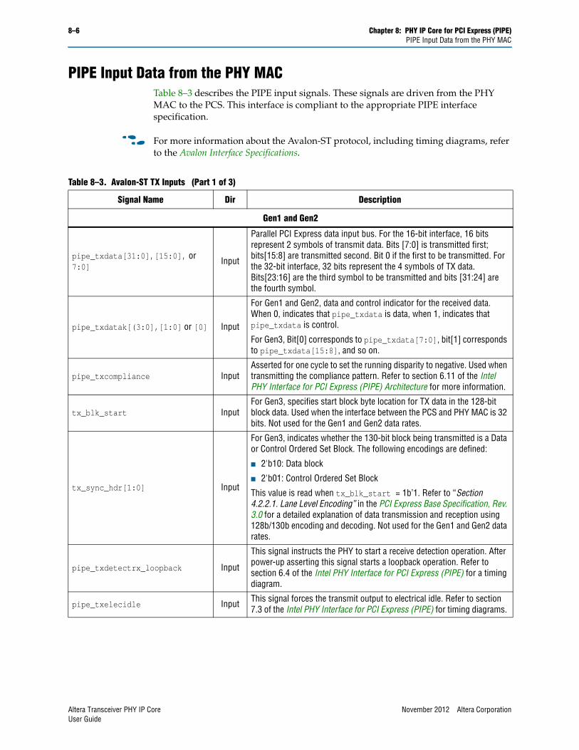
8–6 Chapter 8: PHY IP Core for PCI Express (PIPE)PIPE Input Data from the PHY MAC
PIPE Input Data from the PHY MAC Table 8–3 describes the PIPE input signals. These signals are driven from the PHY MAC to the PCS. This interface is compliant to the appropriate PIPE interface specification.
f For more information about the Avalon-ST protocol, including timing diagrams, refer to the Avalon Interface Specifications.
Table 8–3. Avalon-ST TX Inputs (Part 1 of 3)
Signal Name Dir Description
Gen1 and Gen2
pipe_txdata[31:0],[15:0], or 7:0]
Input
Parallel PCI Express data input bus. For the 16-bit interface, 16 bits represent 2 symbols of transmit data. Bits [7:0] is transmitted first; bits[15:8] are transmitted second. Bit 0 if the first to be transmitted. For the 32-bit interface, 32 bits represent the 4 symbols of TX data. Bits[23:16] are the third symbol to be transmitted and bits [31:24] are the fourth symbol.
pipe_txdatak[(3:0],[1:0] or [0] Input
For Gen1 and Gen2, data and control indicator for the received data. When 0, indicates that pipe_txdata is data, when 1, indicates that pipe_txdata is control.
For Gen3, Bit[0] corresponds to pipe_txdata[7:0], bit[1] corresponds to pipe_txdata[15:8], and so on.
pipe_txcompliance InputAsserted for one cycle to set the running disparity to negative. Used when transmitting the compliance pattern. Refer to section 6.11 of the Intel PHY Interface for PCI Express (PIPE) Architecture for more information.
tx_blk_start InputFor Gen3, specifies start block byte location for TX data in the 128-bit block data. Used when the interface between the PCS and PHY MAC is 32 bits. Not used for the Gen1 and Gen2 data rates.
tx_sync_hdr[1:0] Input
For Gen3, indicates whether the 130-bit block being transmitted is a Data or Control Ordered Set Block. The following encodings are defined:
■ 2'b10: Data block
■ 2'b01: Control Ordered Set Block
This value is read when tx_blk_start = 1b’1. Refer to “Section 4.2.2.1. Lane Level Encoding” in the PCI Express Base Specification, Rev. 3.0 for a detailed explanation of data transmission and reception using 128b/130b encoding and decoding. Not used for the Gen1 and Gen2 data rates.
pipe_txdetectrx_loopback Input
This signal instructs the PHY to start a receive detection operation. After power-up asserting this signal starts a loopback operation. Refer to section 6.4 of the Intel PHY Interface for PCI Express (PIPE) for a timing diagram.
pipe_txelecidle Input This signal forces the transmit output to electrical idle. Refer to section 7.3 of the Intel PHY Interface for PCI Express (PIPE) for timing diagrams.
Altera Transceiver PHY IP Core November 2012 Altera CorporationUser Guide
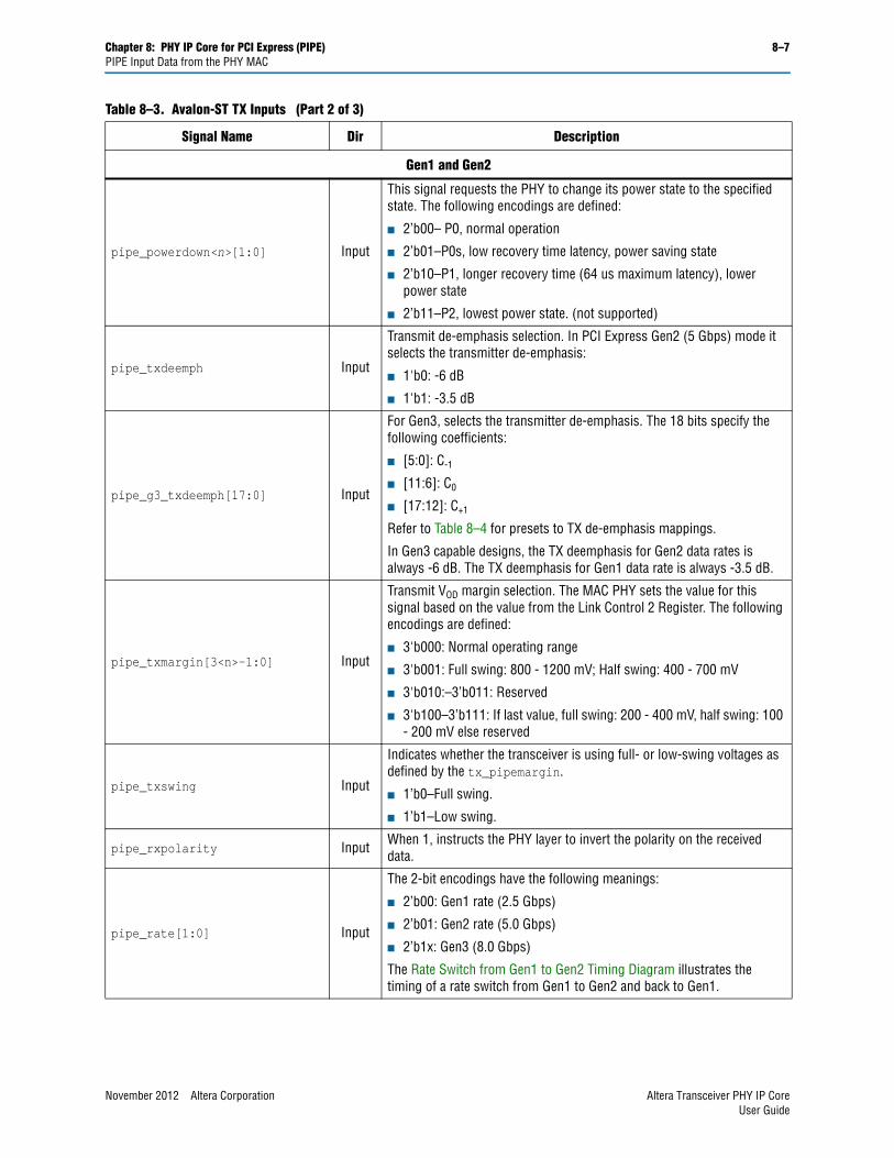
Chapter 8: PHY IP Core for PCI Express (PIPE) 8–7PIPE Input Data from the PHY MAC
pipe_powerdown<n>[1:0] Input
This signal requests the PHY to change its power state to the specified state. The following encodings are defined:
■ 2’b00– P0, normal operation
■ 2’b01–P0s, low recovery time latency, power saving state
■ 2’b10–P1, longer recovery time (64 us maximum latency), lower power state
■ 2’b11–P2, lowest power state. (not supported)
pipe_txdeemph Input
Transmit de-emphasis selection. In PCI Express Gen2 (5 Gbps) mode it selects the transmitter de-emphasis:
■ 1'b0: -6 dB
■ 1'b1: -3.5 dB
pipe_g3_txdeemph[17:0] Input
For Gen3, selects the transmitter de-emphasis. The 18 bits specify the following coefficients:
■ [5:0]: C-1
■ [11:6]: C0
■ [17:12]: C+1
Refer to Table 8–4 for presets to TX de-emphasis mappings.
In Gen3 capable designs, the TX deemphasis for Gen2 data rates is always -6 dB. The TX deemphasis for Gen1 data rate is always -3.5 dB.
pipe_txmargin[3<n>-1:0] Input
Transmit VOD margin selection. The MAC PHY sets the value for this signal based on the value from the Link Control 2 Register. The following encodings are defined:
■ 3'b000: Normal operating range
■ 3'b001: Full swing: 800 - 1200 mV; Half swing: 400 - 700 mV
■ 3'b010:–3’b011: Reserved
■ 3'b100–3’b111: If last value, full swing: 200 - 400 mV, half swing: 100 - 200 mV else reserved
pipe_txswing Input
Indicates whether the transceiver is using full- or low-swing voltages as defined by the tx_pipemargin.
■ 1’b0–Full swing.
■ 1’b1–Low swing.
pipe_rxpolarity Input When 1, instructs the PHY layer to invert the polarity on the received data.
pipe_rate[1:0] Input
The 2-bit encodings have the following meanings:
■ 2’b00: Gen1 rate (2.5 Gbps)
■ 2’b01: Gen2 rate (5.0 Gbps)
■ 2’b1x: Gen3 (8.0 Gbps)
The Rate Switch from Gen1 to Gen2 Timing Diagram illustrates the timing of a rate switch from Gen1 to Gen2 and back to Gen1.
Table 8–3. Avalon-ST TX Inputs (Part 2 of 3)
Signal Name Dir Description
Gen1 and Gen2
November 2012 Altera Corporation Altera Transceiver PHY IP CoreUser Guide
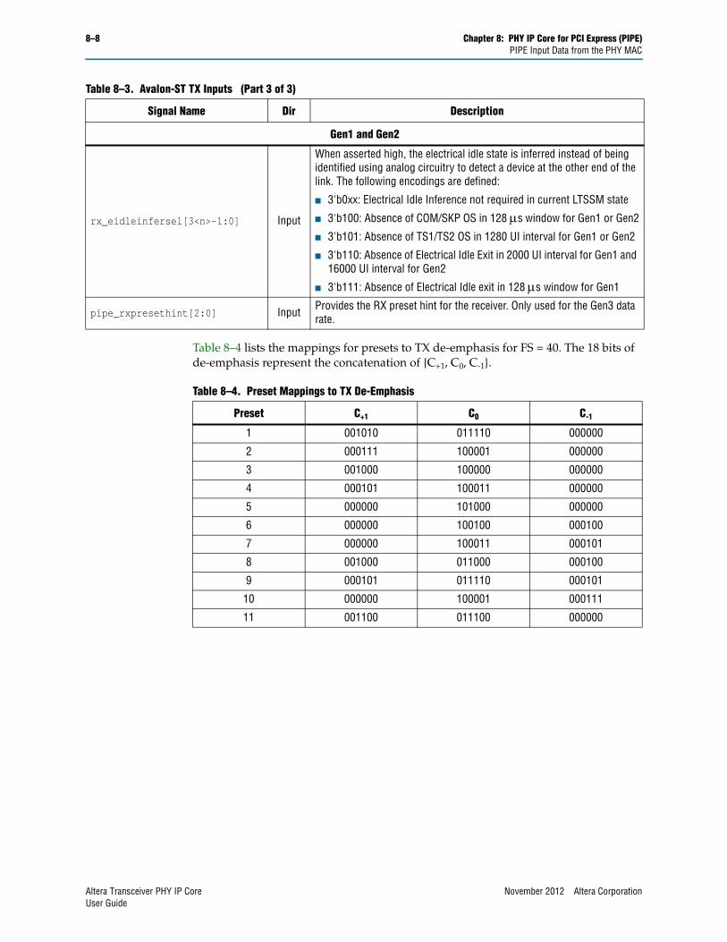
8–8 Chapter 8: PHY IP Core for PCI Express (PIPE)PIPE Input Data from the PHY MAC
Table 8–4 lists the mappings for presets to TX de-emphasis for FS = 40. The 18 bits of de-emphasis represent the concatenation of {C+1, C0, C-1}.
rx_eidleinfersel[3<n>-1:0] Input
When asserted high, the electrical idle state is inferred instead of being identified using analog circuitry to detect a device at the other end of the link. The following encodings are defined:
■ 3'b0xx: Electrical Idle Inference not required in current LTSSM state
■ 3'b100: Absence of COM/SKP OS in 128 s window for Gen1 or Gen2
■ 3'b101: Absence of TS1/TS2 OS in 1280 UI interval for Gen1 or Gen2
■ 3'b110: Absence of Electrical Idle Exit in 2000 UI interval for Gen1 and 16000 UI interval for Gen2
■ 3'b111: Absence of Electrical Idle exit in 128 s window for Gen1
pipe_rxpresethint[2:0] Input Provides the RX preset hint for the receiver. Only used for the Gen3 data rate.
Table 8–3. Avalon-ST TX Inputs (Part 3 of 3)
Signal Name Dir Description
Gen1 and Gen2
Table 8–4. Preset Mappings to TX De-Emphasis
Preset C+1 C0 C-1
1 001010 011110 000000
2 000111 100001 000000
3 001000 100000 000000
4 000101 100011 000000
5 000000 101000 000000
6 000000 100100 000100
7 000000 100011 000101
8 001000 011000 000100
9 000101 011110 000101
10 000000 100001 000111
11 001100 011100 000000
Altera Transceiver PHY IP Core November 2012 Altera CorporationUser Guide
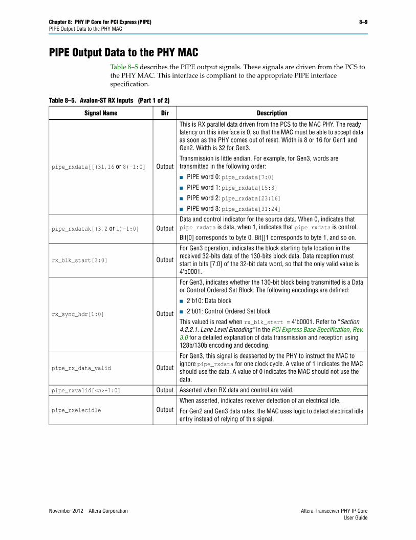
Chapter 8: PHY IP Core for PCI Express (PIPE) 8–9PIPE Output Data to the PHY MAC
PIPE Output Data to the PHY MACTable 8–5 describes the PIPE output signals. These signals are driven from the PCS to the PHY MAC. This interface is compliant to the appropriate PIPE interface specification.
Table 8–5. Avalon-ST RX Inputs (Part 1 of 2)
Signal Name Dir Description
pipe_rxdata[[(31,16 or 8)-1:0] Output
This is RX parallel data driven from the PCS to the MAC PHY. The ready latency on this interface is 0, so that the MAC must be able to accept data as soon as the PHY comes out of reset. Width is 8 or 16 for Gen1 and Gen2. Width is 32 for Gen3.
Transmission is little endian. For example, for Gen3, words are transmitted in the following order:
■ PIPE word 0: pipe_rxdata[7:0]
■ PIPE word 1: pipe_rxdata[15:8]
■ PIPE word 2: pipe_rxdata[23:16]
■ PIPE word 3: pipe_rxdata[31:24]
pipe_rxdatak[(3,2 or 1)-1:0] OutputData and control indicator for the source data. When 0, indicates that pipe_rxdata is data, when 1, indicates that pipe_rxdata is control.
Bit[0] corresponds to byte 0. Bit[]1 corresponds to byte 1, and so on.
rx_blk_start[3:0] Output
For Gen3 operation, indicates the block starting byte location in the received 32-bits data of the 130-bits block data. Data reception must start in bits [7:0] of the 32-bit data word, so that the only valid value is 4’b0001.
rx_sync_hdr[1:0] Output
For Gen3, indicates whether the 130-bit block being transmitted is a Data or Control Ordered Set Block. The following encodings are defined:
■ 2'b10: Data block
■ 2'b01: Control Ordered Set block
This valued is read when rx_blk_start = 4'b0001. Refer to “Section 4.2.2.1. Lane Level Encoding” in the PCI Express Base Specification, Rev. 3.0 for a detailed explanation of data transmission and reception using 128b/130b encoding and decoding.
pipe_rx_data_valid Output
For Gen3, this signal is deasserted by the PHY to instruct the MAC to ignore pipe_rxdata for one clock cycle. A value of 1 indicates the MAC should use the data. A value of 0 indicates the MAC should not use the data.
pipe_rxvalid[<n>-1:0] Output Asserted when RX data and control are valid.
pipe_rxelecidle OutputWhen asserted, indicates receiver detection of an electrical idle.
For Gen2 and Gen3 data rates, the MAC uses logic to detect electrical idle entry instead of relying of this signal.
November 2012 Altera Corporation Altera Transceiver PHY IP CoreUser Guide
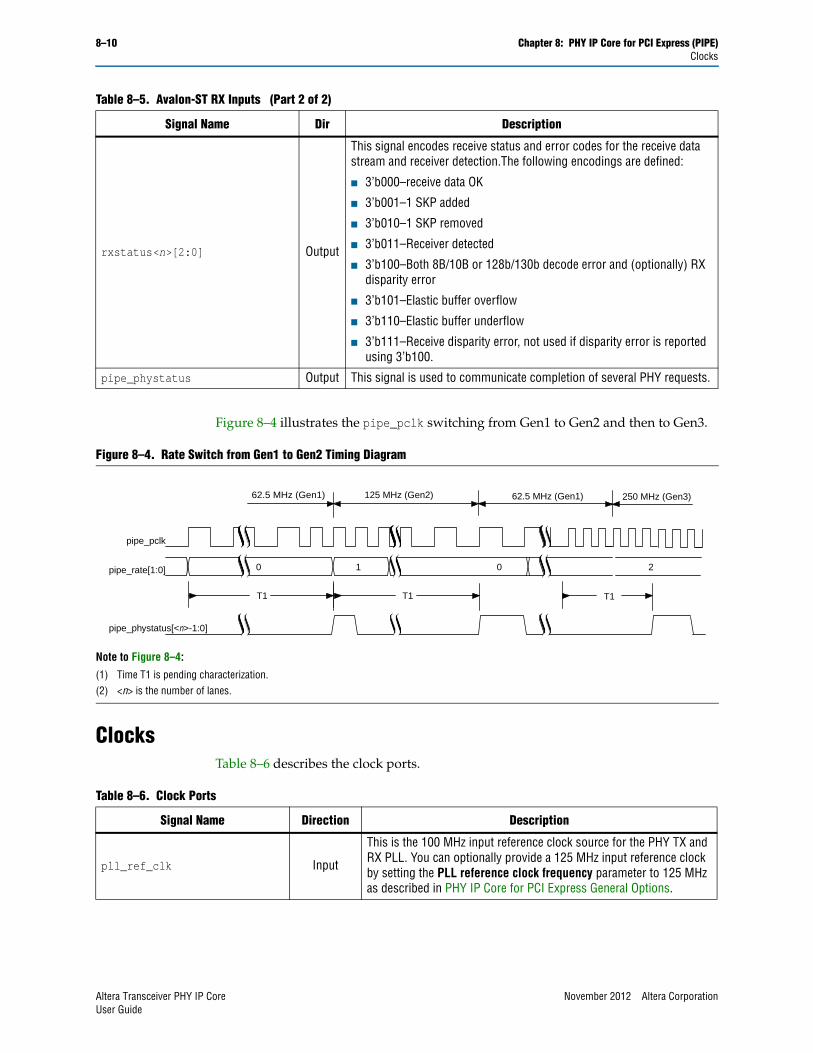
8–10 Chapter 8: PHY IP Core for PCI Express (PIPE)Clocks
Figure 8–4 illustrates the pipe_pclk switching from Gen1 to Gen2 and then to Gen3.
ClocksTable 8–6 describes the clock ports.
rxstatus<n>[2:0] Output
This signal encodes receive status and error codes for the receive data stream and receiver detection.The following encodings are defined:
■ 3’b000–receive data OK
■ 3’b001–1 SKP added
■ 3’b010–1 SKP removed
■ 3’b011–Receiver detected
■ 3’b100–Both 8B/10B or 128b/130b decode error and (optionally) RX disparity error
■ 3’b101–Elastic buffer overflow
■ 3’b110–Elastic buffer underflow
■ 3’b111–Receive disparity error, not used if disparity error is reported using 3’b100.
pipe_phystatus Output This signal is used to communicate completion of several PHY requests.
Table 8–5. Avalon-ST RX Inputs (Part 2 of 2)
Signal Name Dir Description
Figure 8–4. Rate Switch from Gen1 to Gen2 Timing Diagram
Note to Figure 8–4:
(1) Time T1 is pending characterization. (2) <n> is the number of lanes.
pipe_pclk
pipe_rate[1:0] 0 1 0 2
T1 T1 T1
62.5 MHz (Gen1) 62.5 MHz (Gen1) 250 MHz (Gen3)125 MHz (Gen2)
pipe_phystatus[<n>-1:0]
Table 8–6. Clock Ports
Signal Name Direction Description
pll_ref_clk Input
This is the 100 MHz input reference clock source for the PHY TX and RX PLL. You can optionally provide a 125 MHz input reference clock by setting the PLL reference clock frequency parameter to 125 MHz as described in PHY IP Core for PCI Express General Options.
Altera Transceiver PHY IP Core November 2012 Altera CorporationUser Guide
Chapter 8: PHY IP Core for PCI Express (PIPE) 8–11Optional Status Interface
Table 8–7 lists the pipe_pclk frequencies for all available PCS interface widths. Doubling the FPGA transceiver width haves the required frequency.
Optional Status InterfaceTable 8–8 describes the signals the optional status signals.
fixedclk Input A 100 MHz or 125 MHz clock used for the receiver detect circuitry. This clock can be derived from pll_ref_clk.
pipe_pclk Output
Generated in the PMA and driven to the MAC PHY interface. All data and status signals are synchronous to pipe_pclk. This clock has the following frequencies:
■ Gen1: 62.5 MHz
■ Gen2:125 MHz
■ Gen3: 250 MHz
Table 8–6. Clock Ports
Signal Name Direction Description
Table 8–7. pipe_pclk Frequencies
Capability FPGA Transceiver Width Gen1 Gen2 Gen3
Gen1 only8 bits 250 MHz — —
16 bits 125 MHz — —
Gen2 capable 16 bits 125 MHz 250 MHz —
Gen3 capable 32 bits 62.5 MHz 125 MHz 250MHz
Table 8–8. Status Signals (1)
Signal Name Direction Signal Name
tx_ready Output When asserted, indicates that the TX interface has exited the reset state and is ready to transmit.
rx_ready Output When asserted, indicates that the RX interface has exited the reset state and is ready to receive.
pll_locked[<p>-1:0] Output When asserted, indicates that the TX PLL is locked to the input reference clock. This signal is asynchronous.
rx_is_lockedtodata[<n>-1:0] OutputWhen asserted, the receiver CDR is in to lock-to-data mode. When deasserted, the receiver CDR lock mode depends on the rx_locktorefclk signal level.
rx_is_lockedtoref[<n>-1:0] Output Asserted when the receiver CDR is locked to the input reference clock. This signal is asynchronous.
rx_syncstatus[<d><n>/8-1:0] OutputIndicates presence or absence of synchronization on the RX interface. Asserted when word aligner identifies the word alignment pattern or synchronization code groups in the received data stream.
rx_signaldetect[<d><n>/8-1:0]
Output When asserted indicates that the lane detects a sender at the other end of the link.
Note to Table 8–8:
(1) <n> is the number of lanes. <d> is the deserialization factor. <p> is the number of PLLs.
November 2012 Altera Corporation Altera Transceiver PHY IP CoreUser Guide
8–12 Chapter 8: PHY IP Core for PCI Express (PIPE)Serial Data Interface
Serial Data Interface Table 8–9 describes the differential serial TX and RX connections to FPGA pins.
For information about channel placement, refer to “Transceiver Clocking and Channel Placement Guidelines” in the Transceiver Configurations in Arria V GZ Devices or “Transceiver Clocking and Channel Placement Guidelines” in the Transceiver Configurations in Stratix V Devices as appropriate.
1 For soft IP implementations of PCI Express, channel placement is determined by the Quartus II fitter.
f For information about channel placement of the Hard IP PCI Express IP Core, refer to the Channel Placement Gen1 and Gen2 and Channel Placement Gen3 sections in the Stratix V Hard IP for PCI Express User Guide.
Register Interface and Register DescriptionsThe Avalon-MM PHY management interface provides access to the PHY IP Core for PCI Express PCS and PMA features that are not part of the standard PIPE interface. You can use an embedded controller acting as an Avalon-MM master to send read and write commands to this Avalon-MM slave interface.
Table 8–9. Transceiver Differential Serial Interface
Signal Name Direction Description
rx_serial_data[<n>-1:0] Input Receiver differential serial input data, <n> is the number of lanes.
tx_serial_data[<n>-1:0] Output Transmitter differential serial output data <n> is the number of lanes.
Altera Transceiver PHY IP Core November 2012 Altera CorporationUser Guide
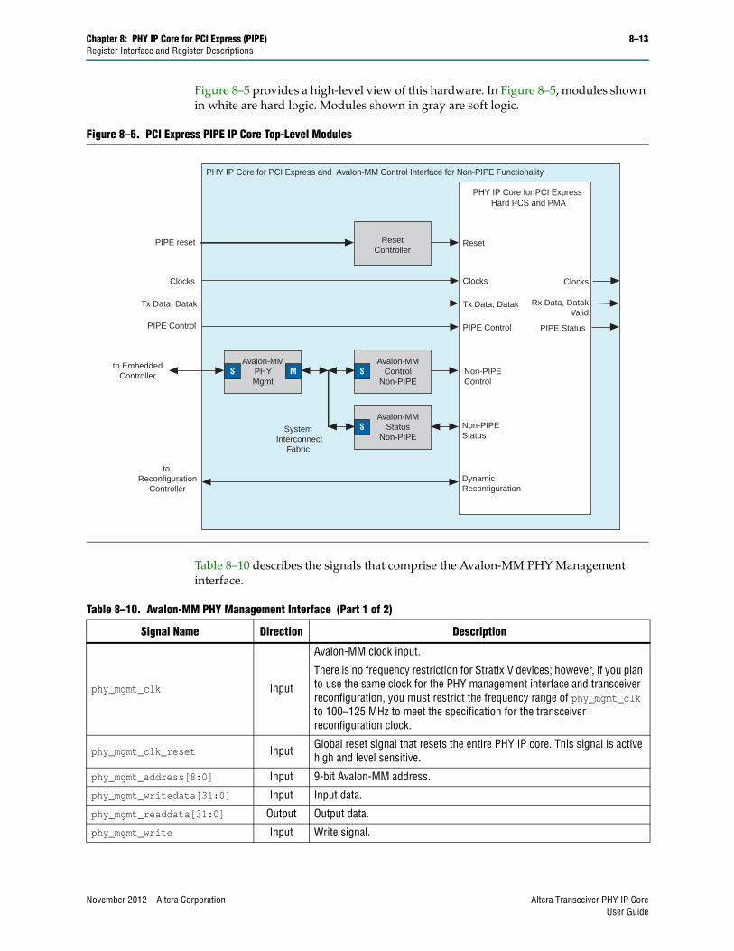
Chapter 8: PHY IP Core for PCI Express (PIPE) 8–13Register Interface and Register Descriptions
Figure 8–5 provides a high-level view of this hardware. In Figure 8–5, modules shown in white are hard logic. Modules shown in gray are soft logic.
Table 8–10 describes the signals that comprise the Avalon-MM PHY Management interface.
Figure 8–5. PCI Express PIPE IP Core Top-Level Modules
System Interconnect
Fabric
to EmbeddedController
to Reconfiguration
Controller
Clocks
Tx Data, Datak
PIPE Control
PHY IP Core for PCI Express Hard PCS and PMA
PHY IP Core for PCI Express and Avalon-MM Control Interface for Non-PIPE Functionality
DynamicReconfiguration
PIPE Control
Tx Data, Datak
Clocks
PIPE Status
Rx Data, Datak Valid
Clocks
Reset
Non-PIPEStatus
Non-PIPEControl
SAvalon-MM
ControlNon-PIPE
SAvalon-MM
StatusNon-PIPE
ResetController
PIPE reset
MAvalon-MM
PHYMgmt
S
Table 8–10. Avalon-MM PHY Management Interface (Part 1 of 2)
Signal Name Direction Description
phy_mgmt_clk Input
Avalon-MM clock input.
There is no frequency restriction for Stratix V devices; however, if you plan to use the same clock for the PHY management interface and transceiver reconfiguration, you must restrict the frequency range of phy_mgmt_clk to 100–125 MHz to meet the specification for the transceiver reconfiguration clock.
phy_mgmt_clk_reset Input Global reset signal that resets the entire PHY IP core. This signal is active high and level sensitive.
phy_mgmt_address[8:0] Input 9-bit Avalon-MM address.
phy_mgmt_writedata[31:0] Input Input data.
phy_mgmt_readdata[31:0] Output Output data.
phy_mgmt_write Input Write signal.
November 2012 Altera Corporation Altera Transceiver PHY IP CoreUser Guide
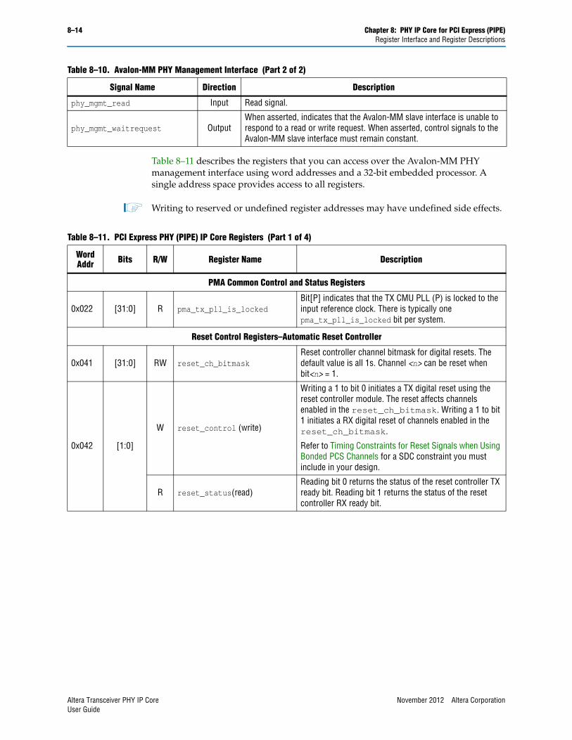
8–14 Chapter 8: PHY IP Core for PCI Express (PIPE)Register Interface and Register Descriptions
Table 8–11 describes the registers that you can access over the Avalon-MM PHY management interface using word addresses and a 32-bit embedded processor. A single address space provides access to all registers.
1 Writing to reserved or undefined register addresses may have undefined side effects.
phy_mgmt_read Input Read signal.
phy_mgmt_waitrequest OutputWhen asserted, indicates that the Avalon-MM slave interface is unable to respond to a read or write request. When asserted, control signals to the Avalon-MM slave interface must remain constant.
Table 8–10. Avalon-MM PHY Management Interface (Part 2 of 2)
Signal Name Direction Description
Table 8–11. PCI Express PHY (PIPE) IP Core Registers (Part 1 of 4)
Word Addr Bits R/W Register Name Description
PMA Common Control and Status Registers
0x022 [31:0] R pma_tx_pll_is_lockedBit[P] indicates that the TX CMU PLL (P) is locked to the input reference clock. There is typically one pma_tx_pll_is_locked bit per system.
Reset Control Registers–Automatic Reset Controller
0x041 [31:0] RW reset_ch_bitmaskReset controller channel bitmask for digital resets. The default value is all 1s. Channel <n> can be reset when bit<n> = 1.
0x042 [1:0]
W reset_control (write)
Writing a 1 to bit 0 initiates a TX digital reset using the reset controller module. The reset affects channels enabled in the reset_ch_bitmask. Writing a 1 to bit 1 initiates a RX digital reset of channels enabled in the reset_ch_bitmask.
Refer to Timing Constraints for Reset Signals when Using Bonded PCS Channels for a SDC constraint you must include in your design.
R reset_status(read)Reading bit 0 returns the status of the reset controller TX ready bit. Reading bit 1 returns the status of the reset controller RX ready bit.
Altera Transceiver PHY IP Core November 2012 Altera CorporationUser Guide
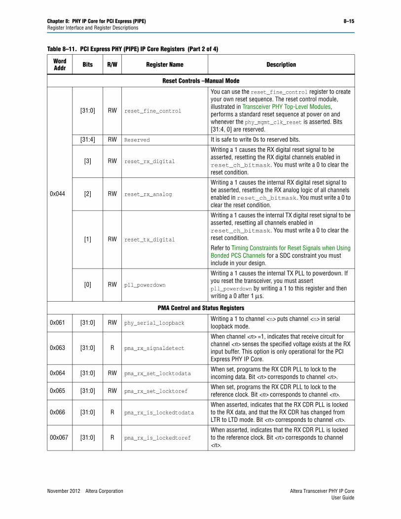
Chapter 8: PHY IP Core for PCI Express (PIPE) 8–15Register Interface and Register Descriptions
Reset Controls –Manual Mode
0x044
[31:0] RW reset_fine_control
You can use the reset_fine_control register to create your own reset sequence. The reset control module, illustrated in Transceiver PHY Top-Level Modules, performs a standard reset sequence at power on and whenever the phy_mgmt_clk_reset is asserted. Bits [31:4, 0] are reserved.
[31:4] RW Reserved It is safe to write 0s to reserved bits.
[3] RW reset_rx_digital
Writing a 1 causes the RX digital reset signal to be asserted, resetting the RX digital channels enabled in reset_ch_bitmask. You must write a 0 to clear the reset condition.
[2] RW reset_rx_analog
Writing a 1 causes the internal RX digital reset signal to be asserted, resetting the RX analog logic of all channels enabled in reset_ch_bitmask. You must write a 0 to clear the reset condition.
[1] RW reset_tx_digital
Writing a 1 causes the internal TX digital reset signal to be asserted, resetting all channels enabled in reset_ch_bitmask. You must write a 0 to clear the reset condition.
Refer to Timing Constraints for Reset Signals when Using Bonded PCS Channels for a SDC constraint you must include in your design.
[0] RW pll_powerdown
Writing a 1 causes the internal TX PLL to powerdown. If you reset the transceiver, you must assert pll_powerdown by writing a 1 to this register and then writing a 0 after 1 s.
PMA Control and Status Registers
0x061 [31:0] RW phy_serial_loopback Writing a 1 to channel <n> puts channel <n> in serial loopback mode.
0x063 [31:0] R pma_rx_signaldetect
When channel <n> =1, indicates that receive circuit for channel <n> senses the specified voltage exists at the RX input buffer. This option is only operational for the PCI Express PHY IP Core.
0x064 [31:0] RW pma_rx_set_locktodataWhen set, programs the RX CDR PLL to lock to the incoming data. Bit <n> corresponds to channel <n>.
0x065 [31:0] RW pma_rx_set_locktorefWhen set, programs the RX CDR PLL to lock to the reference clock. Bit <n> corresponds to channel <n>.
0x066 [31:0] R pma_rx_is_lockedtodataWhen asserted, indicates that the RX CDR PLL is locked to the RX data, and that the RX CDR has changed from LTR to LTD mode. Bit <n> corresponds to channel <n>.
00x067 [31:0] R pma_rx_is_lockedtorefWhen asserted, indicates that the RX CDR PLL is locked to the reference clock. Bit <n> corresponds to channel <n>.
Table 8–11. PCI Express PHY (PIPE) IP Core Registers (Part 2 of 4)
Word Addr Bits R/W Register Name Description
November 2012 Altera Corporation Altera Transceiver PHY IP CoreUser Guide
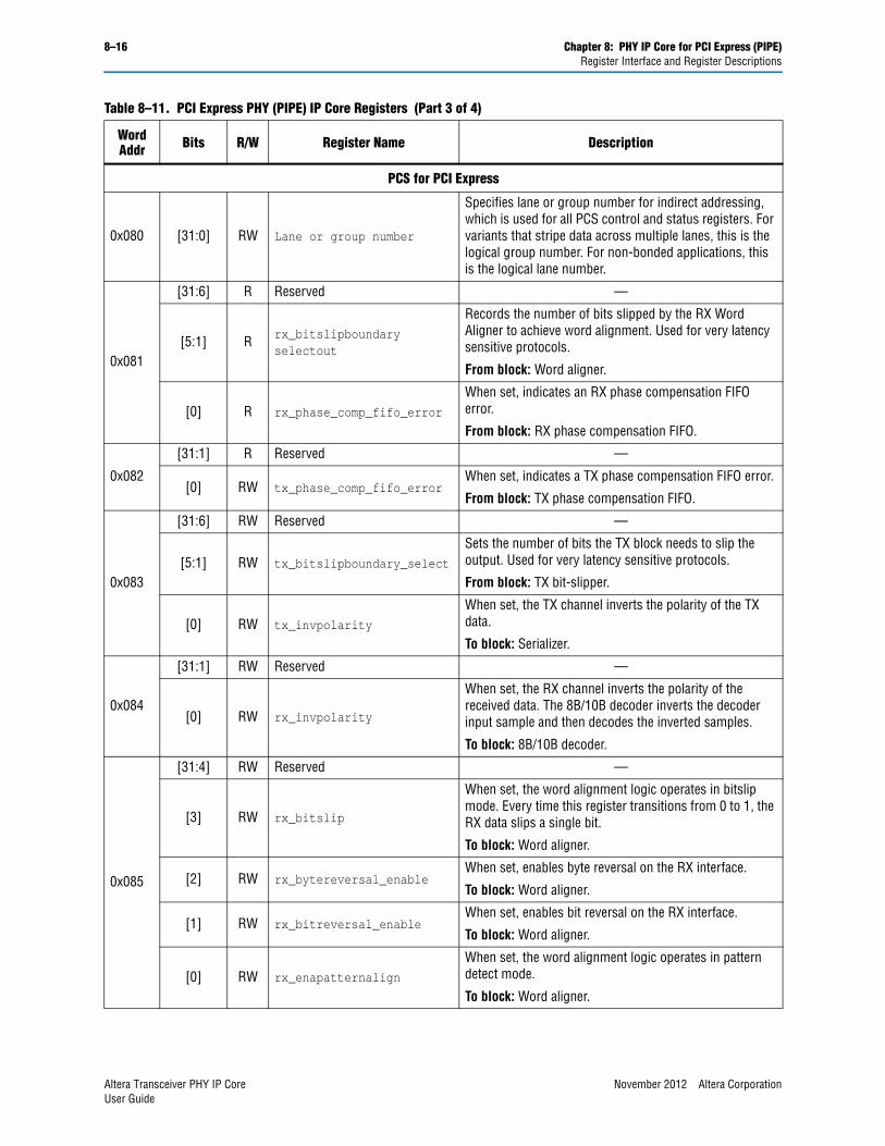
8–16 Chapter 8: PHY IP Core for PCI Express (PIPE)Register Interface and Register Descriptions
PCS for PCI Express
0x080 [31:0] RW Lane or group number
Specifies lane or group number for indirect addressing, which is used for all PCS control and status registers. For variants that stripe data across multiple lanes, this is the logical group number. For non-bonded applications, this is the logical lane number.
0x081
[31:6] R Reserved —
[5:1] R rx_bitslipboundaryselectout
Records the number of bits slipped by the RX Word Aligner to achieve word alignment. Used for very latency sensitive protocols.
From block: Word aligner.
[0] R rx_phase_comp_fifo_error
When set, indicates an RX phase compensation FIFO error.
From block: RX phase compensation FIFO.
0x082
[31:1] R Reserved —
[0] RW tx_phase_comp_fifo_errorWhen set, indicates a TX phase compensation FIFO error.
From block: TX phase compensation FIFO.
0x083
[31:6] RW Reserved —
[5:1] RW tx_bitslipboundary_select
Sets the number of bits the TX block needs to slip the output. Used for very latency sensitive protocols.
From block: TX bit-slipper.
[0] RW tx_invpolarity
When set, the TX channel inverts the polarity of the TX data.
To block: Serializer.
0x084
[31:1] RW Reserved —
[0] RW rx_invpolarity
When set, the RX channel inverts the polarity of the received data. The 8B/10B decoder inverts the decoder input sample and then decodes the inverted samples.
To block: 8B/10B decoder.
0x085
[31:4] RW Reserved —
[3] RW rx_bitslip
When set, the word alignment logic operates in bitslip mode. Every time this register transitions from 0 to 1, the RX data slips a single bit.
To block: Word aligner.
[2] RW rx_bytereversal_enableWhen set, enables byte reversal on the RX interface.
To block: Word aligner.
[1] RW rx_bitreversal_enableWhen set, enables bit reversal on the RX interface.
To block: Word aligner.
[0] RW rx_enapatternalign
When set, the word alignment logic operates in pattern detect mode.
To block: Word aligner.
Table 8–11. PCI Express PHY (PIPE) IP Core Registers (Part 3 of 4)
Word Addr Bits R/W Register Name Description
Altera Transceiver PHY IP Core November 2012 Altera CorporationUser Guide
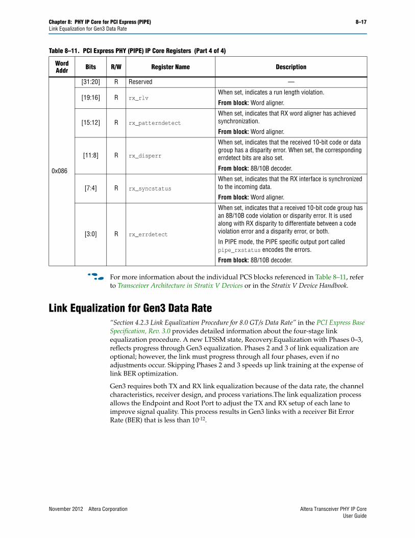
Chapter 8: PHY IP Core for PCI Express (PIPE) 8–17Link Equalization for Gen3 Data Rate
f For more information about the individual PCS blocks referenced in Table 8–11, refer to Transceiver Architecture in Stratix V Devices or in the Stratix V Device Handbook.
Link Equalization for Gen3 Data Rate“Section 4.2.3 Link Equalization Procedure for 8.0 GT/s Data Rate” in the PCI Express Base Specification, Rev. 3.0 provides detailed information about the four-stage link equalization procedure. A new LTSSM state, Recovery.Equalization with Phases 0–3, reflects progress through Gen3 equalization. Phases 2 and 3 of link equalization are optional; however, the link must progress through all four phases, even if no adjustments occur. Skipping Phases 2 and 3 speeds up link training at the expense of link BER optimization.
Gen3 requires both TX and RX link equalization because of the data rate, the channel characteristics, receiver design, and process variations.The link equalization process allows the Endpoint and Root Port to adjust the TX and RX setup of each lane to improve signal quality. This process results in Gen3 links with a receiver Bit Error Rate (BER) that is less than 10-12.
0x086
[31:20] R Reserved —
[19:16] R rx_rlvWhen set, indicates a run length violation.
From block: Word aligner.
[15:12] R rx_patterndetect
When set, indicates that RX word aligner has achieved synchronization.
From block: Word aligner.
[11:8] R rx_disperr
When set, indicates that the received 10-bit code or data group has a disparity error. When set, the corresponding errdetect bits are also set.
From block: 8B/10B decoder.
[7:4] R rx_syncstatus
When set, indicates that the RX interface is synchronized to the incoming data.
From block: Word aligner.
[3:0] R rx_errdetect
When set, indicates that a received 10-bit code group has an 8B/10B code violation or disparity error. It is used along with RX disparity to differentiate between a code violation error and a disparity error, or both.
In PIPE mode, the PIPE specific output port called pipe_rxstatus encodes the errors.
From block: 8B/10B decoder.
Table 8–11. PCI Express PHY (PIPE) IP Core Registers (Part 4 of 4)
Word Addr Bits R/W Register Name Description
November 2012 Altera Corporation Altera Transceiver PHY IP CoreUser Guide
8–18 Chapter 8: PHY IP Core for PCI Express (PIPE)Link Equalization for Gen3 Data Rate
Phase 0Phase 0 includes the following steps:
1. Upstream component enters Phase 0 of equalization during Recovery.Rcvrconfig by sending EQ TS2 training sets with starting presets for the downstream component. EQ TS2 training sets may be sent at 2.5 GT/s or 5 GT/s.
2. The downstream component enters Phase 0 of equalization after exiting Recovery.Speed at 8 GT/s. It receives the starting presets from the training sequences and applies them to its transmitter. At this time, upstream component has entered Phase 1 and is operating at 8 GT/s.
3. To move to Phase 1, the receiver must have a BER < 10-4 and should be able to decode enough consecutive training sequences.
4. The downstream component must detect training sets with Equalization Control (EC) bits set to 2’b01 in order to move to EQ Phase 1.
Phase 1During Phase 1 of equalization process, the link partners exchange FS (Full Swing) and LF (Low Frequency) information. These values represent the upper and lower bounds for the TX coefficients. The receiver uses this information to calculate and request the next set of transmitter coefficients.
1. Once training sets with EC bits set to 1’b0 are captured on all lanes, the upstream component moves to EQ Phase 2 sending EC=2’b10 along with starting pre-cursor, main cursor, and post-cursor coefficients.
2. The downstream component detects these new training sets, and moves to EQ Phase 2.
Phase 2 (Optional)During Phase 2, the Endpoint tunes the TX coefficients of the Root Port. The TS1 Use Preset bit determines whether the Endpoint uses presets for coarse resolution or coefficients for fine resolution.
1 If you are using the PHY IP Core for PCI Express (PIPE) PCI Express as an Endpoint, you cannot perform Phase 2 tuning. The PIPE interface does not provide any measurement metric to the Root Port to guide coefficient preset decision making. The Root Port should reflect the existing coefficients and move to the next phase. The default Full Swing (FS) value advertized by Altera device is 40 and Low Frequency (LF) is 13.
If you are using the PHY IP Core for PCI Express (PIPE) PCI Express as Root Port, the End Point can tune the Root Port TX coefficients.
Altera Transceiver PHY IP Core November 2012 Altera CorporationUser Guide

Chapter 8: PHY IP Core for PCI Express (PIPE) 8–19Link Equalization for Gen3 Data Rate
The tuning sequence typically includes the following steps:
1. The Endpoint receives the starting presets from the Phase 2 training sets sent by the Root Port.
2. The circuitry in the Endpoint receiver determines the BER and calculates the next set of transmitter coefficients using FS and LF and embeds this information in the Training Sets for the Link Partner to apply to its transmitter.
The Root Port decodes these coefficients and presets, performs legality checks for the three transmitter coefficient rules and applies the settings to its transmitter and also sends them in the Training Sets. Three rules for transmitter coefficients are:
a. |C-1| <= Floor (FS/4)
b. |C-1|+C0+|C+1| = FS
c. C0-|C-1|-|C+1 |>= LF
Where:
C0 is the main cursor (boost)
C-1 is the pre-cursor (pre shoot)
C+1 is the post-cursor (de emphasis)
3. This process is repeated until the downstream component's receiver achieves a BER of < 10-12.
Phase 3 (Optional)During this phase, the Root Port tunes the Endpoint’s transmitter. This process is analogous to Phase 2 but operates in the opposite direction.
1 If you are using the PHY IP Core for PCI Express (PIPE) PCI Express as a Root Port, you cannot perform Phase 3 tuning.
Once Phase 3 tuning is complete, the Root Port moves to Recovery.RcvrLock, sending EC=2’b00, along with the final coefficients or preset agreed upon in Phase 2. The Endpoint moves to Recovery.RcvrLock using the final coefficients or preset agreed upon in Phase 3.
Recommendations for Tuning Link Partner’s TransmitterTo improve the BER of the StratixV receiver, Altera recommends that you turn on Adaptive Equalization (AEQ) one-time mode during Phase 2 Equalization for Endpoints or Phase 3 Equalization for Root Ports. You enable AEQ through the Transceiver Reconfiguration Controller IP Core. For more information about this component, refer to Transceiver Reconfiguration Controller IP Core. For more information about running AEQ, refer to AEQ Registers.
1 AEQ must be turned off while switching from Gen3 to Gen1 or from Gen3 to Gen2.
November 2012 Altera Corporation Altera Transceiver PHY IP CoreUser Guide
8–20 Chapter 8: PHY IP Core for PCI Express (PIPE)Enabling Dynamic PMA Tuning for PCIe Gen3
Enabling Dynamic PMA Tuning for PCIe Gen3 “Section 4.2.3 Link Equalization Procedure for 8.0 GT/s Data Rate” in the PCI Express Base Specification, Rev. 3.0 provides detailed information about the four-stage link equalization procedure. However, in some instances you may want to override the specified four-stage link equalization procedure to dynamically tune PMA settings.
Follow these steps to override Gen3 equalization:
1. Connect the Transceiver Reconfiguration Controller IP Core to your PHY IP Core for PCI Express as shown in PCI Express PIPE IP Core Top-Level Modules.
2. For each transmitter port, use the Quartus II Assignment Editor to assign the Transmitter VOD/Preemphasis Control Source the value RAM_CTL.
3. Recompile your design.
You can now use the Transceiver Reconfiguration Controller to change VOD and pre-emphasis settings.
Dynamic ReconfigurationThe calibration performed by the dynamic reconfiguration interface compensates for variations due to process, voltage, and temperature (PVT). For Stratix V devices, each channel and each TX PLL have separate dynamic reconfiguration interfaces. The MegaWizard Plug-In Manager provides informational messages on the connectivity of these interfaces. Example 8–1 shows the messages for a 8-channel PHY IP Core for PCI Express (PIPE).
Although you must initially create a separate reconfiguration interface for each channel and TX PLL in your design, when the Quartus II software compiles your design, it reduces the total number of reconfiguration interfaces by merging reconfiguration interfaces. The synthesized design typically includes a reconfiguration interface for at least three channels because the three channels within each transceiver triplet share a single physical Avalon-MM slave interface which connects to the Transceiver Reconfiguration Controller IP Core. Conversely, you cannot connect the three channels that share this single physical Avalon-MM interface to different Transceiver Reconfiguration Controllers. Doing so causes a Fitter error. For more information, refer to“Transceiver Reconfiguration Controller to PHY IP Connectivity”.
Example 8–1. Informational Messages for the Transceiver Reconfiguration Interface
PHY IP will require 9 reconfiguration interfaces for connection to the external reconfiguration controller.Reconfiguration interface offsets 0-7 are connected to the transceiver channels.Reconfiguration interface offset 8 is connected to the transmit PLL.
Altera Transceiver PHY IP Core November 2012 Altera CorporationUser Guide
Chapter 8: PHY IP Core for PCI Express (PIPE) 8–21Simulation Files and Example Testbench
Table 8–12 describes the signals in the reconfiguration interface. This interface uses the Avalon-MM PHY Management interface clock.
Logical Lane Assignment Restriction If you are using ×6 or ×N bonding, transceiver dynamic reconfiguration requires that you assign the starting channel number. Transceiver dynamic reconfiguration requires that you assign the starting channel number. For PCIe ×8 configurations, logical channel 0 must be assigned to either physical transceiver channel 1 or channel 4 of a transceiver bank. For PCIe x4 configurations, logical channel 1 must be assigned to either physical transceiver channel 1 or channel 4 of a transceiver bank. However, if you have already created a PCB with a different lane assignment for PCIe ×8 logical lane 0 or PCIe ×4 logical lane 1, you can use the workaound shown in Example 8–2 to remove this restriction. Example 8–2 redefines the pma_bonding_master parameter using the Quartus II Assignment Editor. In this example, the pma_bonding_master was originally assigned to physical channel 1. (The original assignment could also have been to physical channel 4.) The to parameter reassigns the pma_bonding_master to the PHY IP Core for PCI Express (PIPE) instance name. You must substitute the instance name from your design for the instance name shown in quotation marks
Simulation Files and Example Testbench Refer to Running a Simulation Testbench for a description of the directories and files that the Quartus II software creates automatically when you generate your PHY IP Core for PCI Express.
f Refer to the Altera wiki for an example testbench that you can use as a starting point in creating your own verification environment.
Table 8–12. Reconfiguration Interface
Signal Name Direction Description
reconfig_to_xcvr [<r>70-1:0] InputReconfiguration signals from the Transceiver Reconfiguration Controller. <r> grows linearly with the number of reconfiguration interfaces.
reconfig_from_xcvr [<r>46-1:0] OutputReconfiguration signals to the Transceiver Reconfiguration Controller. <r> grows linearly with the number of reconfiguration interfaces.
Example 8–2. Overriding Logical Channel 0 Channel Assignment Restrictions in Stratix V Devices for ×6 or ×N Bonding
set_parameter -name pma_bonding_master "\"1\"" -to "<PHY IP instance name>"
November 2012 Altera Corporation Altera Transceiver PHY IP CoreUser Guide

8–22 Chapter 8: PHY IP Core for PCI Express (PIPE)Simulation Files and Example Testbench
Altera Transceiver PHY IP Core November 2012 Altera CorporationUser Guide
November 2012 Altera Corporation
9. Custom PHY IP Core
The Altera Custom PHY IP Core is a generic PHY that you can customize for use in Arria V, Cyclone V, or Stratix V FPGAs. You can connect your application’s MAC-layer logic to the Custom PHY to transmit and receive data at rates of 0.611–6.5536 Gbps for Arria V GX devices, 0.611–10.3125 Gbps in Arria V GT devices, 0.622–9.8304 Gbps in Arria V GZ devices, 0.611–3.125 Gbps for Cyclone V GX devices, 0.611–5.000 Gbps for Cyclone V GT devices, and 0.622–11.0 Gbps for Stratix V devices. You can parameterize the physical coding sublayer (PCS) to include the functions that your application requires. The following functions are available:
■ 8B/10B encode and decode
■ Three word alignment modes
■ Rate matching
■ Byte ordering
By setting the appropriate options using the MegaWizard Plug-In Manager, you can configure the Custom PHY IP Core to support many standard protocols, including all of the following protocols:
■ Serial Data Converter (SDC(JESD204A))
■ Serial digital interface (SDI)
■ Ethernet (1.25 and 2.50 Gbps)
■ Serial RapidIO® (SRIO) 1.3
■ Serial ATA (SATA) and sequential active serial (SAS) Gen1, Gen2, and Gen3
■ Gigabit-capable passive optical network (GPON)
To access control and status registers in the Custom PHY, your design must include an embedded controller with an Avalon-MM master interface. This is a standard, memory-mapped protocol that is typically used to read and write registers and memory.
f For more information about the Avalon-ST and Avalon-MM protocols, refer to the Avalon Interface Specifications.
Altera Transceiver PHY IP CoreUser Guide
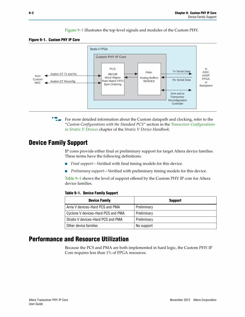
9–2 Chapter 9: Custom PHY IP CoreDevice Family Support
Figure 9–1 illustrates the top-level signals and modules of the Custom PHY.
f For more detailed information about the Custom datapath and clocking, refer to the “Custom Configurations with the Standard PCS” section in the Transceiver Configurations in Stratix V Devices chapter of the Stratix V Device Handbook.
Device Family SupportIP cores provide either final or preliminary support for target Altera device families. These terms have the following definitions:
■ Final support—Verified with final timing models for this device.
■ Preliminary support—Verified with preliminary timing models for this device.
Table 9–1 shows the level of support offered by the Custom PHY IP core for Altera device families.
Performance and Resource UtilizationBecause the PCS and PMA are both implemented in hard logic, the Custom PHY IP Core requires less than 1% of FPGA resources.
Figure 9–1. Custom PHY IP Core
Custom PHY IP Core
Tx Serial DataAvalon-ST Tx and Rx
Rx Serial Data
toASIC,ASSP,FPGA,
orBackplane
fromCustom
MAC
Stratix V FPGA
PCS:
8B/10BWord Aligner
Rate Match FIFOByte Ordering
PMA:
Analog BuffersSERDESAvalon-ST Reconfig
from and toTransceiver
ReconfigurationController
Table 9–1. Device Family Support
Device Family Support
Arria V devices–Hard PCS and PMA Preliminary
Cyclone V devices–Hard PCS and PMA Preliminary
Stratix V devices–Hard PCS and PMA Preliminary
Other device families No support
Altera Transceiver PHY IP Core November 2012 Altera CorporationUser Guide
Chapter 9: Custom PHY IP Core 9–3Parameterizing the Custom PHY
Parameterizing the Custom PHY Complete the following steps to configure the Custom PHY IP Core in the MegaWizard Plug-In Manager:
1. For Which device family will you be using?, select Stratix V.
2. Click Installed Plug-Ins > Interfaces > Transceiver PHY > Custom PHY v12.1.
3. Use the tabs on the MegaWizard Plug-In Manager to select the options required for the protocol.
4. Refer to the following topics to learn more about the parameters:
a. General Options Parameters
b. Word Alignment Parameters
c. Rate Match FIFO Parameters
d. 8B/10B Encoder and Decoder Parameters
e. Byte Order Parameters
f. PLL Reconfiguration Parameters
g. Analog Parameters
5. Click Finish to generate your parameterized Custom PHY IP Core.
1 Presets are available for the 1.25 Gbps Ethernet (GIGE–1.25 Gbps) and 2.50 Gbps Ethernet (GIGE–2.5 Gbps) protocols.
General Options ParametersThe General Options tab allows you to set the basic parameters of your transceiver PHY. Table 9–2 lists the settings available on the General Options tab.
Table 9–2. Custom PHY General Options (Part 1 of 4)
Name Value Description
Device familyArria V
Cyclone VStratix V
Specifies the device family. Arria V, Cyclone V, and Stratix V are available.
Parameter validation rules CustomGIGE
Allows you to specify the transceiver protocol. Select Custom if you are not implementing 1.25 or 2.50GIGE.
Mode of operationDuplex
TXRX
You can select to transmit data, receive data, or both.
Number of lanes 1–32 The total number of lanes in each direction.
Enable lane bonding On/OffWhen enabled, a single clock drives multiple lanes, reducing clock skew. In Stratix V devices, up to 6 lanes can be bonded if you use an ATX PLL; 4 lanes can be bonded if you select the CMU PLL.
November 2012 Altera Corporation Altera Transceiver PHY IP CoreUser Guide
9–4 Chapter 9: Custom PHY IP CoreGeneral Options Parameters
Bonding mode×1
×Nfb_compensation
Select ×1 to use separate clock sources for each channel. (This option is available for Cyclone V and Arria V devices.)
Select ×N to use the same clock source for up to 6 channels in a single transceiver bank, resulting in reduced clock skew. You must use contiguous channels when you select ×N bonding. In addition, you must place logical channel 0 in either physical channel 1 or 4. Physical channels 1 and 4 are indirect drivers of the ×N clock network.
Select fb_compensation (feedback compensation) to use the same clock source for multiple channels across different transceiver banks to reduce clock skew. (This option is only available for Stratix V devices.)
For more information about bonding, refer to “Transmitter Clock Network” in Transceiver Clocking in Arria V Devices in volume 2 of the Arria V Device Handbook.
For more information about bonding, refer to “Transmitter Clock Network” in Transceiver Clocking in Cyclone V Devices in volume 2 of the Cyclone V Device Handbook.
For more information about bonding, refer to “Bonded Channel Configurations Using the PLL Feedback Compensation Path” in Transceiver Clocking in Stratix V Devices in volume 2 of the Stratix V Device Handbook.
FPGA fabric transceiver interface width
8,10,16,20,32,40
Specifies the total serialization factor, from an input or output pin to the MAC-layer logic.
PCS-PMA interface width 8, 10, 16, 20
The PCS-PMA interface width depends on the FPGA fabric transceiver interface width and whether 8B/10B is enabled. The following combinations are available:FPGA/XCVR 8B/10B PCS-PMA Interface Width
8 No 88 Yes 1010 No 1016 No 8 or 1616 Yes 10 or 20 20 No 10 or 2032 No 1632 Yes 2040 No 20
Table 9–2. Custom PHY General Options (Part 2 of 4)
Name Value Description
Altera Transceiver PHY IP Core November 2012 Altera CorporationUser Guide
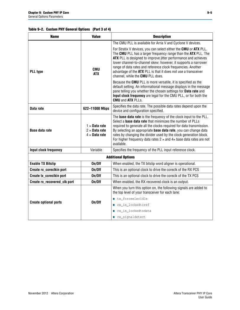
Chapter 9: Custom PHY IP Core 9–5General Options Parameters
PLL type CMUATX
The CMU PLL is available for Arria V and Cyclone V devices.
For Stratix V devices, you can select either the CMU or ATX PLL. The CMU PLL has a larger frequency range than the ATX PLL. The ATX PLL is designed to improve jitter performance and achieves lower channel-to-channel skew; however, it supports a narrower range of data rates and reference clock frequencies. Another advantage of the ATX PLL is that it does not use a transceiver channel, while the CMU PLL does.
Because the CMU PLL is more versatile, it is specified as the default setting. An informational message displays in the message pane telling you whether the chosen settings for Data rate and Input clock frequency are legal for the CMU PLL, or for both the CMU and ATX PLLs.
Data rate 622–11000 Mbps Specifies the data rate. The possible data rates depend upon the device and configuration specified.
Base data rate1 × Data rate2 × Data rate4 × Data rate
The base data rate is the frequency of the clock input to the PLL. Select a base data rate that minimizes the number of PLLs required to generate all the clocks required for data transmission. By selecting an appropriate base data rate, you can change data rates by changing the divider used by the clock generation block. For higher frequency data rates 2 × and 4× base data rates are not available.
Input clock frequency Variable Specifies the frequency of the PLL input reference clock.
Additional Options
Enable TX Bitslip On/Off When enabled, the TX bitslip word aligner is operational.
Create rx_coreclkin port On/Off This is an optional clock to drive the coreclk of the RX PCS
Create tx_coreclkin port On/Off This is an optional clock to drive the coreclk of the TX PCS
Create rx_recovered_clk port On/Off When enabled, the RX recovered clock is an output.
Create optional ports On/Off
When you turn this option on, the following signals are added to the top level of your transceiver for each lane:
■ tx_forceelecidle
■ rx_is_lockedtoref
■ rx_is_lockedtodata
■ rx_signaldetect
Table 9–2. Custom PHY General Options (Part 3 of 4)
Name Value Description
November 2012 Altera Corporation Altera Transceiver PHY IP CoreUser Guide
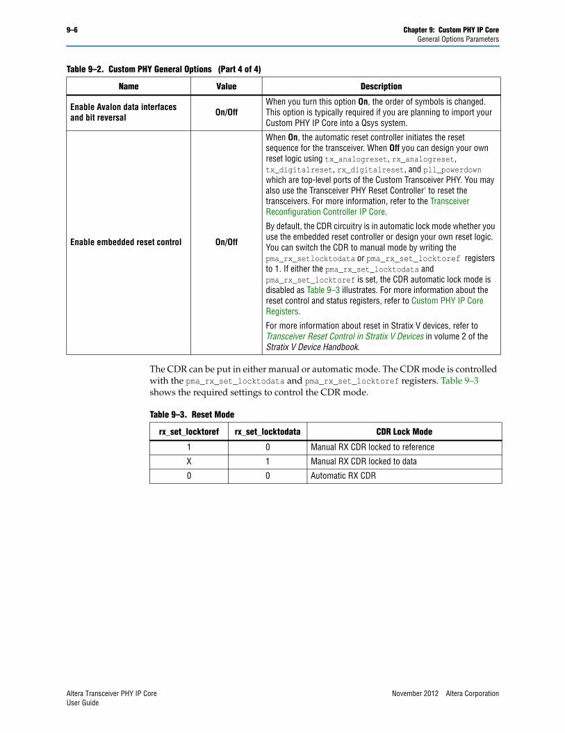
9–6 Chapter 9: Custom PHY IP CoreGeneral Options Parameters
The CDR can be put in either manual or automatic mode. The CDR mode is controlled with the pma_rx_set_locktodata and pma_rx_set_locktoref registers. Table 9–3 shows the required settings to control the CDR mode.
Enable Avalon data interfaces and bit reversal On/Off
When you turn this option On, the order of symbols is changed. This option is typically required if you are planning to import your Custom PHY IP Core into a Qsys system.
Enable embedded reset control On/Off
When On, the automatic reset controller initiates the reset sequence for the transceiver. When Off you can design your own reset logic using tx_analogreset, rx_analogreset, tx_digitalreset, rx_digitalreset, and pll_powerdown which are top-level ports of the Custom Transceiver PHY. You may also use the Transceiver PHY Reset Controller' to reset the transceivers. For more information, refer to the Transceiver Reconfiguration Controller IP Core.
By default, the CDR circuitry is in automatic lock mode whether you use the embedded reset controller or design your own reset logic. You can switch the CDR to manual mode by writing the pma_rx_setlocktodata or pma_rx_set_locktoref registers to 1. If either the pma_rx_set_locktodata and pma_rx_set_locktoref is set, the CDR automatic lock mode is disabled as Table 9–3 illustrates. For more information about the reset control and status registers, refer to Custom PHY IP Core Registers.
For more information about reset in Stratix V devices, refer to Transceiver Reset Control in Stratix V Devices in volume 2 of the Stratix V Device Handbook.
Table 9–2. Custom PHY General Options (Part 4 of 4)
Name Value Description
Table 9–3. Reset Mode
rx_set_locktoref rx_set_locktodata CDR Lock Mode
1 0 Manual RX CDR locked to reference
X 1 Manual RX CDR locked to data
0 0 Automatic RX CDR
Altera Transceiver PHY IP Core November 2012 Altera CorporationUser Guide
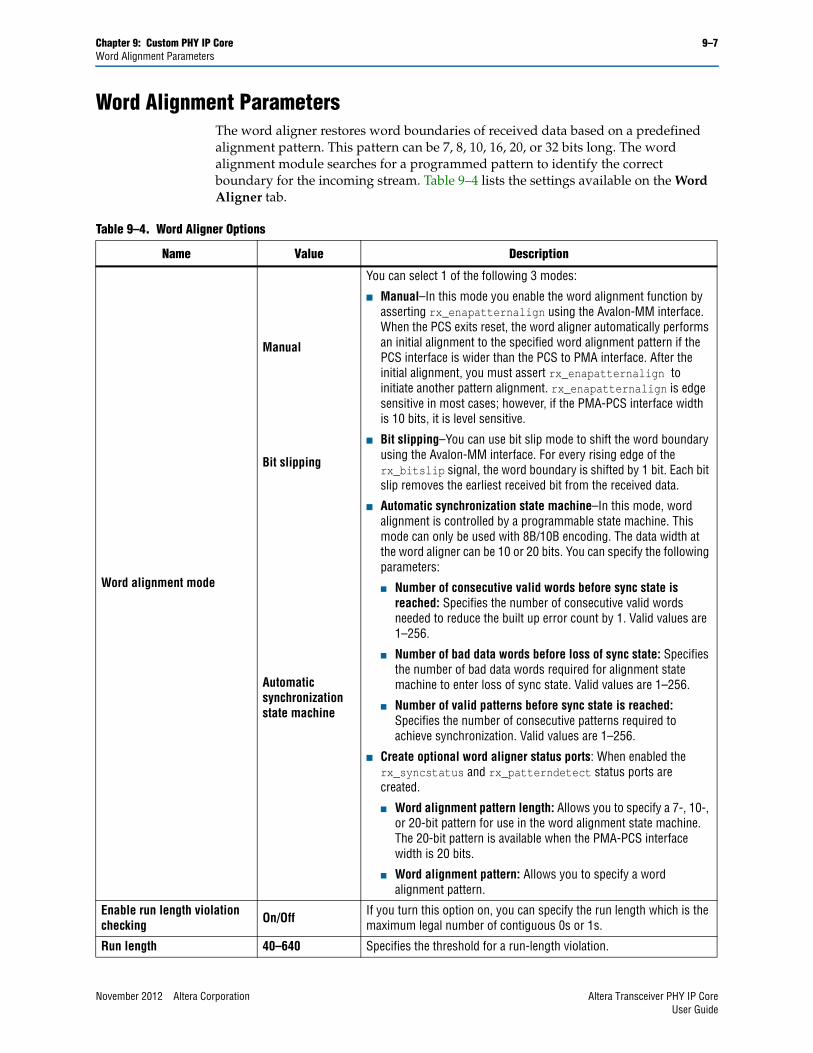
Chapter 9: Custom PHY IP Core 9–7Word Alignment Parameters
Word Alignment ParametersThe word aligner restores word boundaries of received data based on a predefined alignment pattern. This pattern can be 7, 8, 10, 16, 20, or 32 bits long. The word alignment module searches for a programmed pattern to identify the correct boundary for the incoming stream. Table 9–4 lists the settings available on the Word Aligner tab.
Table 9–4. Word Aligner Options
Name Value Description
Word alignment mode
Manual
You can select 1 of the following 3 modes:
■ Manual–In this mode you enable the word alignment function by asserting rx_enapatternalign using the Avalon-MM interface. When the PCS exits reset, the word aligner automatically performs an initial alignment to the specified word alignment pattern if the PCS interface is wider than the PCS to PMA interface. After the initial alignment, you must assert rx_enapatternalign to initiate another pattern alignment. rx_enapatternalign is edge sensitive in most cases; however, if the PMA-PCS interface width is 10 bits, it is level sensitive.
Bit slipping
■ Bit slipping–You can use bit slip mode to shift the word boundary using the Avalon-MM interface. For every rising edge of the rx_bitslip signal, the word boundary is shifted by 1 bit. Each bit slip removes the earliest received bit from the received data.
Automatic synchronization state machine
■ Automatic synchronization state machine–In this mode, word alignment is controlled by a programmable state machine. This mode can only be used with 8B/10B encoding. The data width at the word aligner can be 10 or 20 bits. You can specify the following parameters:
■ Number of consecutive valid words before sync state is reached: Specifies the number of consecutive valid words needed to reduce the built up error count by 1. Valid values are 1–256.
■ Number of bad data words before loss of sync state: Specifies the number of bad data words required for alignment state machine to enter loss of sync state. Valid values are 1–256.
■ Number of valid patterns before sync state is reached: Specifies the number of consecutive patterns required to achieve synchronization. Valid values are 1–256.
■ Create optional word aligner status ports: When enabled the rx_syncstatus and rx_patterndetect status ports are created.
■ Word alignment pattern length: Allows you to specify a 7-, 10-, or 20-bit pattern for use in the word alignment state machine. The 20-bit pattern is available when the PMA-PCS interface width is 20 bits.
■ Word alignment pattern: Allows you to specify a word alignment pattern.
Enable run length violation checking On/Off If you turn this option on, you can specify the run length which is the
maximum legal number of contiguous 0s or 1s.
Run length 40–640 Specifies the threshold for a run-length violation.
November 2012 Altera Corporation Altera Transceiver PHY IP CoreUser Guide
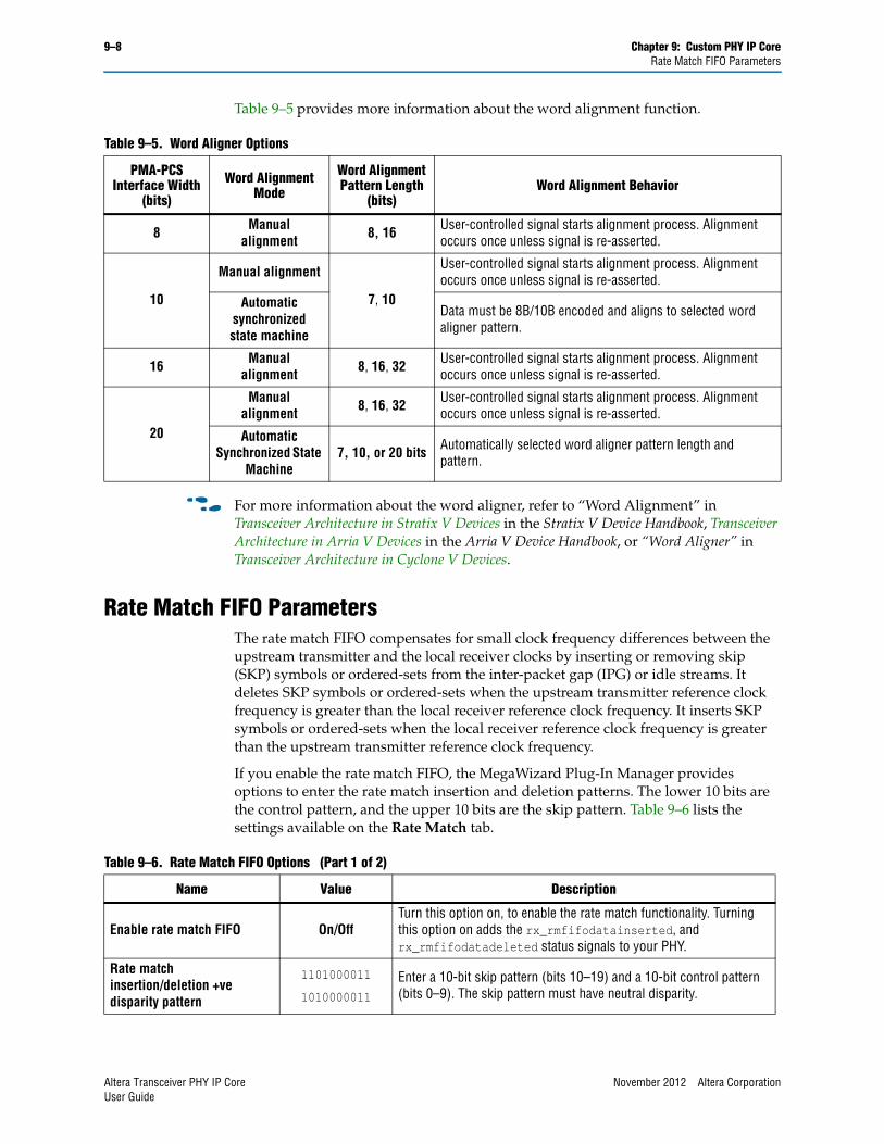
9–8 Chapter 9: Custom PHY IP CoreRate Match FIFO Parameters
Table 9–5 provides more information about the word alignment function.
f For more information about the word aligner, refer to “Word Alignment” in Transceiver Architecture in Stratix V Devices in the Stratix V Device Handbook, Transceiver Architecture in Arria V Devices in the Arria V Device Handbook, or “Word Aligner” in Transceiver Architecture in Cyclone V Devices.
Rate Match FIFO ParametersThe rate match FIFO compensates for small clock frequency differences between the upstream transmitter and the local receiver clocks by inserting or removing skip (SKP) symbols or ordered-sets from the inter-packet gap (IPG) or idle streams. It deletes SKP symbols or ordered-sets when the upstream transmitter reference clock frequency is greater than the local receiver reference clock frequency. It inserts SKP symbols or ordered-sets when the local receiver reference clock frequency is greater than the upstream transmitter reference clock frequency.
If you enable the rate match FIFO, the MegaWizard Plug-In Manager provides options to enter the rate match insertion and deletion patterns. The lower 10 bits are the control pattern, and the upper 10 bits are the skip pattern. Table 9–6 lists the settings available on the Rate Match tab.
Table 9–5. Word Aligner Options
PMA-PCS Interface Width
(bits)
Word Alignment Mode
Word Alignment Pattern Length
(bits)Word Alignment Behavior
8 Manualalignment 8, 16 User-controlled signal starts alignment process. Alignment
occurs once unless signal is re-asserted.
10
Manual alignment
7, 10
User-controlled signal starts alignment process. Alignment occurs once unless signal is re-asserted.
Automatic synchronizedstate machine
Data must be 8B/10B encoded and aligns to selected word aligner pattern.
16 Manualalignment 8, 16, 32 User-controlled signal starts alignment process. Alignment
occurs once unless signal is re-asserted.
20
Manualalignment 8, 16, 32 User-controlled signal starts alignment process. Alignment
occurs once unless signal is re-asserted.
Automatic Synchronized State
Machine7, 10, or 20 bits Automatically selected word aligner pattern length and
pattern.
Table 9–6. Rate Match FIFO Options (Part 1 of 2)
Name Value Description
Enable rate match FIFO On/OffTurn this option on, to enable the rate match functionality. Turning this option on adds the rx_rmfifodatainserted, and rx_rmfifodatadeleted status signals to your PHY.
Rate match insertion/deletion +ve disparity pattern
1101000011
1010000011
Enter a 10-bit skip pattern (bits 10–19) and a 10-bit control pattern (bits 0–9). The skip pattern must have neutral disparity.
Altera Transceiver PHY IP Core November 2012 Altera CorporationUser Guide
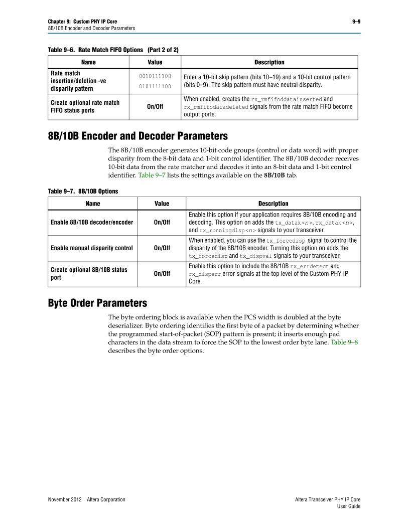
Chapter 9: Custom PHY IP Core 9–98B/10B Encoder and Decoder Parameters
8B/10B Encoder and Decoder ParametersThe 8B/10B encoder generates 10-bit code groups (control or data word) with proper disparity from the 8-bit data and 1-bit control identifier. The 8B/10B decoder receives 10-bit data from the rate matcher and decodes it into an 8-bit data and 1-bit control identifier. Table 9–7 lists the settings available on the 8B/10B tab.
Byte Order ParametersThe byte ordering block is available when the PCS width is doubled at the byte deserializer. Byte ordering identifies the first byte of a packet by determining whether the programmed start-of-packet (SOP) pattern is present; it inserts enough pad characters in the data stream to force the SOP to the lowest order byte lane. Table 9–8 describes the byte order options.
Rate match insertion/deletion -ve disparity pattern
0010111100
0101111100
Enter a 10-bit skip pattern (bits 10–19) and a 10-bit control pattern (bits 0–9). The skip pattern must have neutral disparity.
Create optional rate match FIFO status ports On/Off
When enabled, creates the rx_rmfifoddatainserted and rx_rmfifodatadeleted signals from the rate match FIFO become output ports.
Table 9–6. Rate Match FIFO Options (Part 2 of 2)
Name Value Description
Table 9–7. 8B/10B Options
Name Value Description
Enable 8B/10B decoder/encoder On/OffEnable this option if your application requires 8B/10B encoding and decoding. This option on adds the tx_datak<n>, rx_datak<n>, and rx_runningdisp<n> signals to your transceiver.
Enable manual disparity control On/OffWhen enabled, you can use the tx_forcedisp signal to control the disparity of the 8B/10B encoder. Turning this option on adds the tx_forcedisp and tx_dispval signals to your transceiver.
Create optional 8B/10B status port On/Off
Enable this option to include the 8B/10B rx_errdetect and rx_disperr error signals at the top level of the Custom PHY IP Core.
November 2012 Altera Corporation Altera Transceiver PHY IP CoreUser Guide
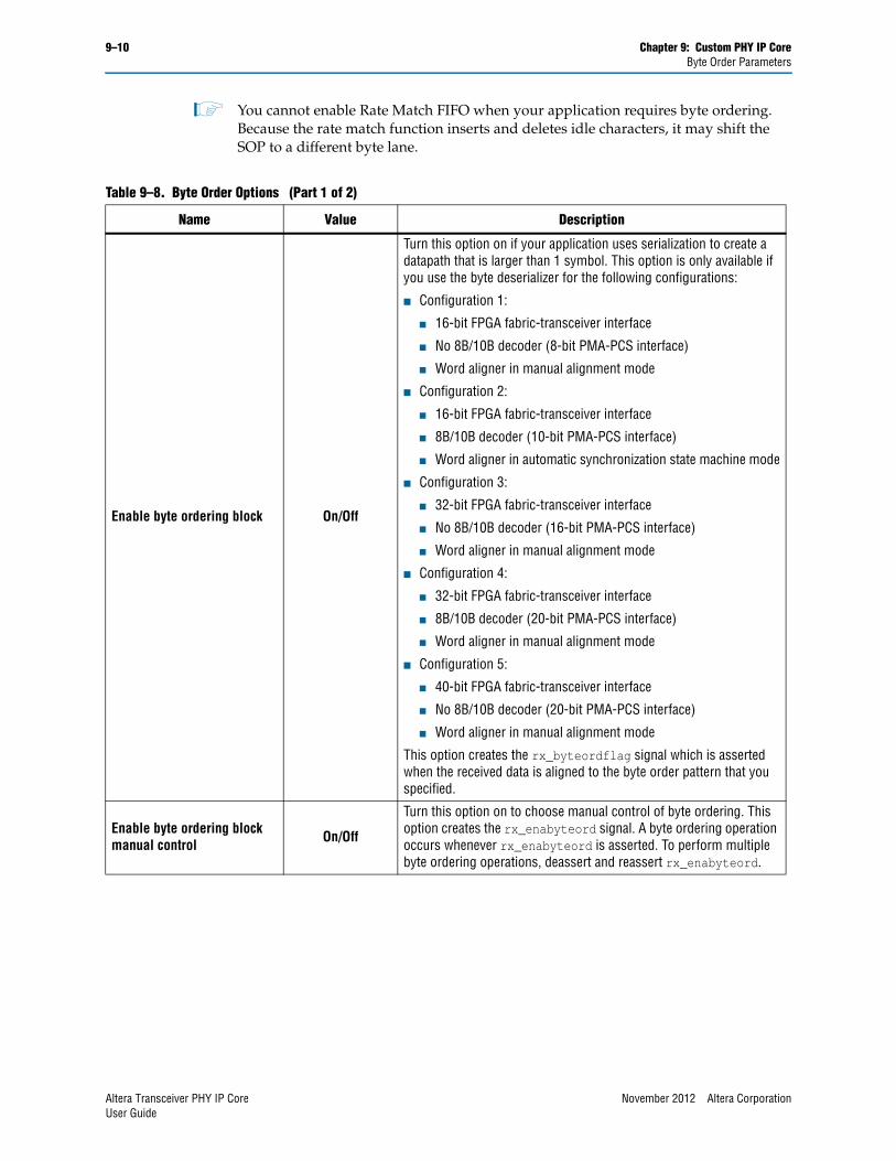
9–10 Chapter 9: Custom PHY IP CoreByte Order Parameters
1 You cannot enable Rate Match FIFO when your application requires byte ordering. Because the rate match function inserts and deletes idle characters, it may shift the SOP to a different byte lane.
Table 9–8. Byte Order Options (Part 1 of 2)
Name Value Description
Enable byte ordering block On/Off
Turn this option on if your application uses serialization to create a datapath that is larger than 1 symbol. This option is only available if you use the byte deserializer for the following configurations:
■ Configuration 1:
■ 16-bit FPGA fabric-transceiver interface
■ No 8B/10B decoder (8-bit PMA-PCS interface)
■ Word aligner in manual alignment mode
■ Configuration 2:
■ 16-bit FPGA fabric-transceiver interface
■ 8B/10B decoder (10-bit PMA-PCS interface)
■ Word aligner in automatic synchronization state machine mode
■ Configuration 3:
■ 32-bit FPGA fabric-transceiver interface
■ No 8B/10B decoder (16-bit PMA-PCS interface)
■ Word aligner in manual alignment mode
■ Configuration 4:
■ 32-bit FPGA fabric-transceiver interface
■ 8B/10B decoder (20-bit PMA-PCS interface)
■ Word aligner in manual alignment mode
■ Configuration 5:
■ 40-bit FPGA fabric-transceiver interface
■ No 8B/10B decoder (20-bit PMA-PCS interface)
■ Word aligner in manual alignment mode
This option creates the rx_byteordflag signal which is asserted when the received data is aligned to the byte order pattern that you specified.
Enable byte ordering block manual control On/Off
Turn this option on to choose manual control of byte ordering. This option creates the rx_enabyteord signal. A byte ordering operation occurs whenever rx_enabyteord is asserted. To perform multiple byte ordering operations, deassert and reassert rx_enabyteord.
Altera Transceiver PHY IP Core November 2012 Altera CorporationUser Guide
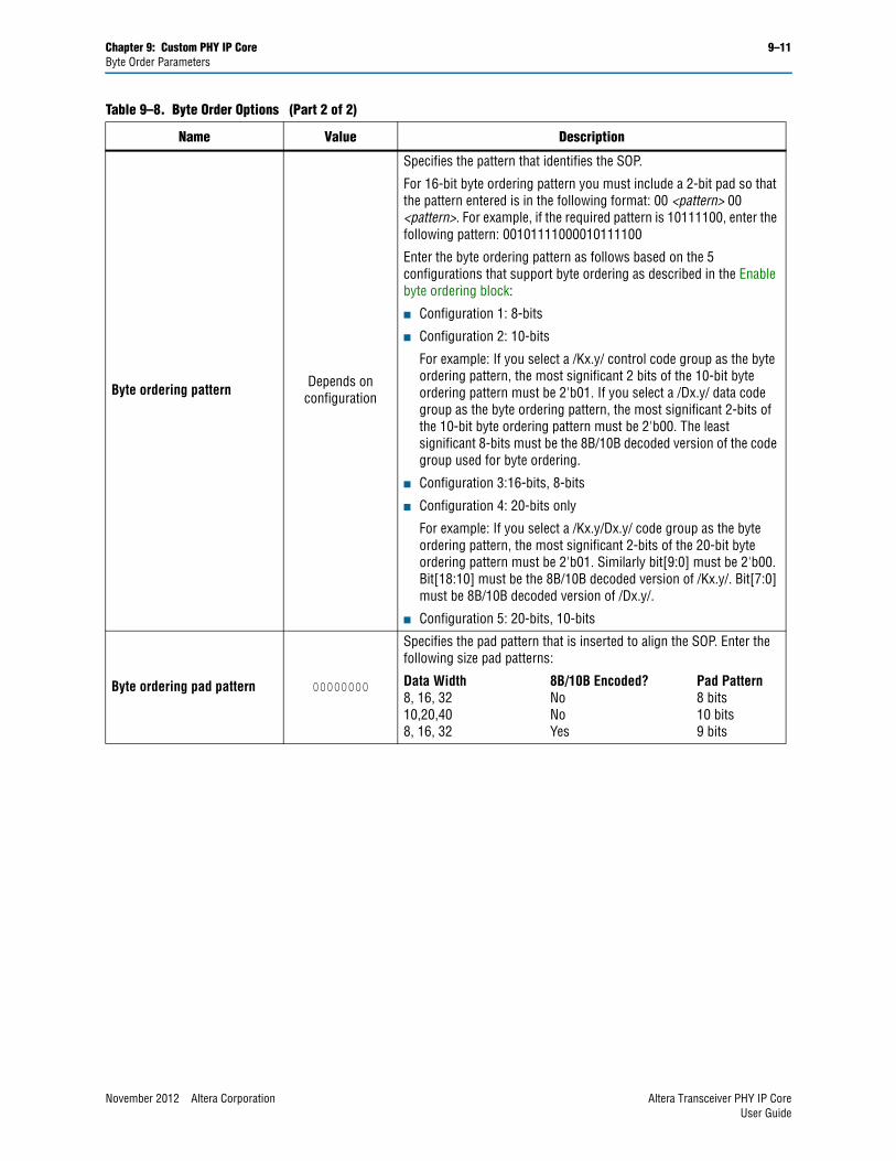
Chapter 9: Custom PHY IP Core 9–11Byte Order Parameters
Byte ordering pattern Depends on configuration
Specifies the pattern that identifies the SOP.
For 16-bit byte ordering pattern you must include a 2-bit pad so that the pattern entered is in the following format: 00 <pattern> 00 <pattern>. For example, if the required pattern is 10111100, enter the following pattern: 00101111000010111100
Enter the byte ordering pattern as follows based on the 5 configurations that support byte ordering as described in the Enable byte ordering block:
■ Configuration 1: 8-bits
■ Configuration 2: 10-bits
For example: If you select a /Kx.y/ control code group as the byte ordering pattern, the most significant 2 bits of the 10-bit byte ordering pattern must be 2'b01. If you select a /Dx.y/ data code group as the byte ordering pattern, the most significant 2-bits of the 10-bit byte ordering pattern must be 2'b00. The least significant 8-bits must be the 8B/10B decoded version of the code group used for byte ordering.
■ Configuration 3:16-bits, 8-bits
■ Configuration 4: 20-bits only
For example: If you select a /Kx.y/Dx.y/ code group as the byte ordering pattern, the most significant 2-bits of the 20-bit byte ordering pattern must be 2'b01. Similarly bit[9:0] must be 2'b00. Bit[18:10] must be the 8B/10B decoded version of /Kx.y/. Bit[7:0] must be 8B/10B decoded version of /Dx.y/.
■ Configuration 5: 20-bits, 10-bits
Byte ordering pad pattern 00000000
Specifies the pad pattern that is inserted to align the SOP. Enter the following size pad patterns:
Data Width 8B/10B Encoded? Pad Pattern8, 16, 32 No 8 bits10,20,40 No 10 bits8, 16, 32 Yes 9 bits
Table 9–8. Byte Order Options (Part 2 of 2)
Name Value Description
November 2012 Altera Corporation Altera Transceiver PHY IP CoreUser Guide
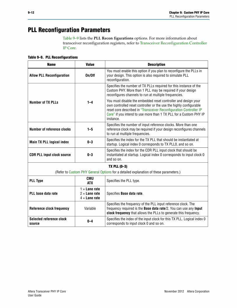
9–12 Chapter 9: Custom PHY IP CorePLL Reconfiguration Parameters
PLL Reconfiguration ParametersTable 9–9 lists the PLL Recon figurations options. For more information about transceiver reconfiguration registers, refer to Transceiver Reconfiguration Controller IP Core.
Table 9–9. PLL Reconfigurations
Name Value Description
Allow PLL Reconfiguration On/OffYou must enable this option if you plan to reconfigure the PLLs in your design. This option is also required to simulate PLL reconfiguration.
Number of TX PLLs 1–4
Specifies the number of TX PLLs required for this instance of the Custom PHY. More than 1 PLL may be required if your design reconfigures channels to run at multiple frequencies.
You must disable the embedded reset controller and design your own controlled reset controller or the use the highly configurable reset core described in “Transceiver Reconfiguration Controller IP Core” if you intend to use more than 1 TX PLL for a Custom PHY IP instance.
Number of reference clocks 1–5Specifies the number of input reference clocks. More than one reference clock may be required if your design reconfigures channels to run at multiple frequencies.
Main TX PLL logical index 0–3 Specifies the index for the TX PLL that should be instantiated at startup. Logical index 0 corresponds to TX PLL0, and so on.
CDR PLL input clock source 0–3Specifies the index for the CDR PLL input clock that should be instantiated at startup. Logical index 0 corresponds to input clock 0 and so on.
TX PLL (0–3)(Refer to Custom PHY General Options for a detailed explanation of these parameters.)
PLL Type CMUATX Specifies the PLL type.
PLL base data rate1 × Lane rate2 × Lane rate4 × Lane rate
Specifies Base data rate.
Reference clock frequency VariableSpecifies the frequency of the PLL input reference clock. The frequency required is the Base data rate/2. You can use any Input clock frequency that allows the PLLs to generate this frequency.
Selected reference clock source 0–4 Specifies the index of the input clock for this TX PLL. Logical index 0
corresponds to input clock 0 and so on.
Altera Transceiver PHY IP Core November 2012 Altera CorporationUser Guide
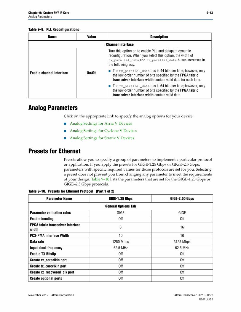
Chapter 9: Custom PHY IP Core 9–13Analog Parameters
Analog ParametersClick on the appropriate link to specify the analog options for your device:
■ Analog Settings for Arria V Devices
■ Analog Settings for Cyclone V Devices
■ Analog Settings for Stratix V Devices
Presets for EthernetPresets allow you to specify a group of parameters to implement a particular protocol or application. If you apply the presets for GIGE-1.25 Gbps or GIGE–2.5 Gbps, parameters with specific required values for those protocols are set for you. Selecting a preset does not prevent you from changing any parameter to meet the requirements of your design. Table 9–10 lists the parameters that are set for the GIGE-1.25 Gbps or GIGE–2.5 Gbps protocols.
Channel Interface
Enable channel interface On/Off
Turn this option on to enable PLL and datapath dynamic reconfiguration. When you select this option, the width of tx_parallel_data and rx_parallel_data buses increases in the following way.
■ The tx_parallel_data bus is 44 bits per lane; however, only the low-order number of bits specified by the FPGA fabric transceiver interface width contain valid data for each lane.
■ The rx_parallel_data bus is 64 bits per lane; however, only the low-order number of bits specified by the FPGA fabric transceiver interface width contain valid data.
Table 9–9. PLL Reconfigurations
Name Value Description
Table 9–10. Presets for Ethernet Protocol (Part 1 of 2)
Parameter Name GIGE-1.25 Gbps GIGE-2.50 Gbps
General Options Tab
Parameter validation rules GIGE GIGE
Enable bonding Off Off
FPGA fabric transceiver interface width 8 16
PCS-PMA Interface Width 10 10
Data rate 1250 Mbps 3125 Mbps
Input clock frequency 62.5 MHz 62.5 MHz
Enable TX Bitslip Off Off
Create rx_coreclkin port Off Off
Create tx_coreclkin port Off Off
Create rx_recovered_clk port Off Off
Create optional ports Off Off
November 2012 Altera Corporation Altera Transceiver PHY IP CoreUser Guide
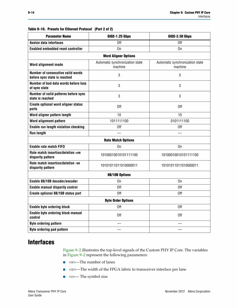
9–14 Chapter 9: Custom PHY IP CoreInterfaces
InterfacesFigure 9–2 illustrates the top-level signals of the Custom PHY IP Core. The variables in Figure 9–2 represent the following parameters:
■ <n>—The number of lanes
■ <w>—The width of the FPGA fabric to transceiver interface per lane
■ <s>— The symbol size
Avalon data interfaces Off Off
Enabled embedded reset controller On On
Word Aligner Options
Word alignment mode Automatic synchronization state machine
Automatic synchronization state machine
Number of consecutive valid words before sync state is reached 3 3
Number of bad data words before loss of sync state 3 3
Number of valid patterns before sync state is reached 3 3
Create optional word aligner status ports Off Off
Word aligner pattern length 10 10
Word alignment pattern 1011111100 0101111100
Enable run length violation checking Off Off
Run length — —
Rate Match Options
Enable rate match FIFO On On
Rate match insertion/deletion +ve disparity pattern 10100010010101111100 10100010010101111100
Rate match insertion/deletion -ve disparity pattern 10101011011010000011 10101011011010000011
8B/10B Options
Enable 8B/10B decoder/encoder On On
Enable manual disparity control Off Off
Create optional 8B/10B status port Off Off
Byte Order Options
Enable byte ordering block Off Off
Enable byte ordering block manual control Off Off
Byte ordering pattern — —
Byte ordering pad pattern — —
Table 9–10. Presets for Ethernet Protocol (Part 2 of 2)
Parameter Name GIGE-1.25 Gbps GIGE-2.50 Gbps
Altera Transceiver PHY IP Core November 2012 Altera CorporationUser Guide
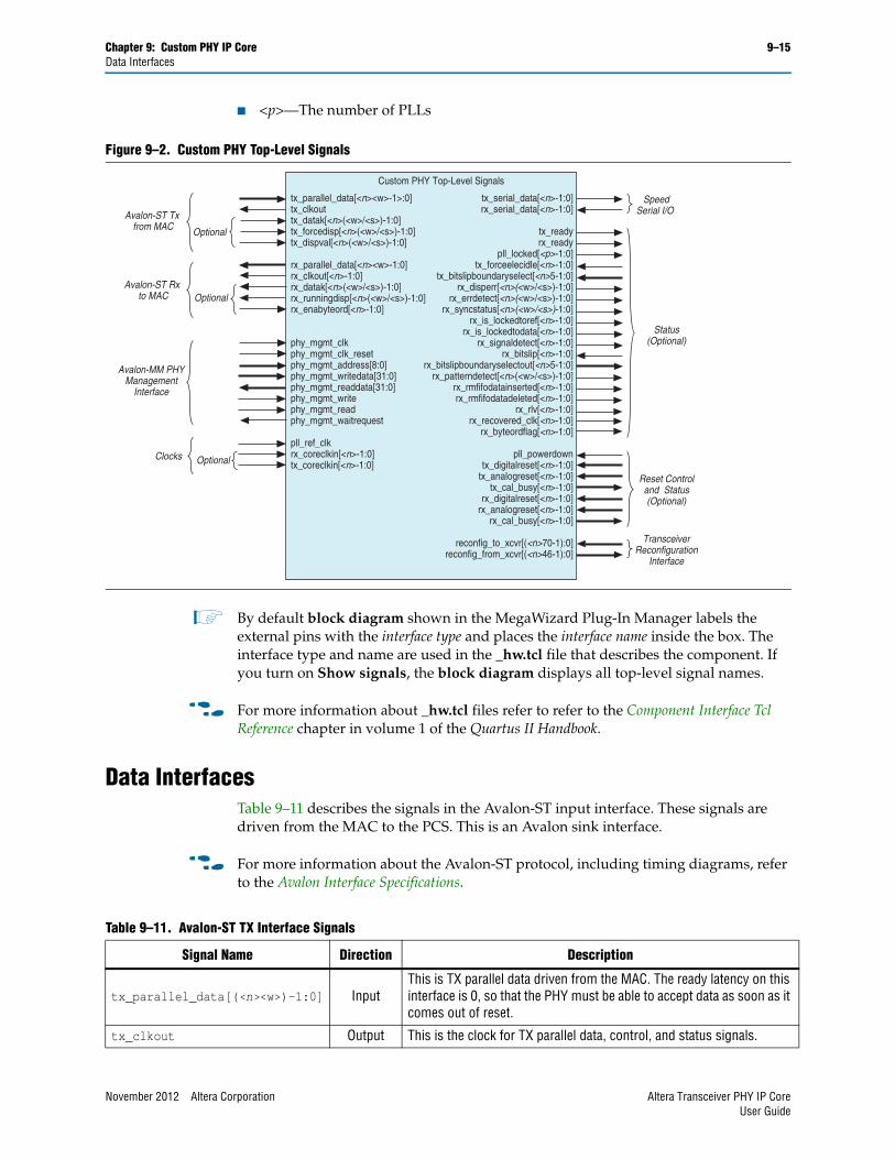
Chapter 9: Custom PHY IP Core 9–15Data Interfaces
■ <p>—The number of PLLs
1 By default block diagram shown in the MegaWizard Plug-In Manager labels the external pins with the interface type and places the interface name inside the box. The interface type and name are used in the _hw.tcl file that describes the component. If you turn on Show signals, the block diagram displays all top-level signal names.
f For more information about _hw.tcl files refer to refer to the Component Interface Tcl Reference chapter in volume 1 of the Quartus II Handbook.
Data InterfacesTable 9–11 describes the signals in the Avalon-ST input interface. These signals are driven from the MAC to the PCS. This is an Avalon sink interface.
f For more information about the Avalon-ST protocol, including timing diagrams, refer to the Avalon Interface Specifications.
Figure 9–2. Custom PHY Top-Level Signals
tx_parallel_data[<n><w>-1>:0]tx_clkout tx_datak[<n>(<w>/<s>)-1:0]tx_forcedisp[<n>(<w>/<s>)-1:0]tx_dispval[<n>(<w>/<s>)-1:0]
rx_parallel_data[<n><w>-1:0]rx_clkout[<n>-1:0]rx_datak[<n>(<w>/<s>)-1:0]rx_runningdisp[<n>(<w>/<s>)-1:0]rx_enabyteord[<n>-1:0]
phy_mgmt_clkphy_mgmt_clk_resetphy_mgmt_address[8:0]phy_mgmt_writedata[31:0]phy_mgmt_readdata[31:0]phy_mgmt_writephy_mgmt_readphy_mgmt_waitrequest
pll_ref_clkrx_coreclkin[<n>-1:0]tx_coreclkin[<n>-1:0]
Custom PHY Top-Level Signals
tx_serial_data[<n>-1:0]rx_serial_data[<n>-1:0]
tx_readyrx_ready
pll_locked[<p>-1:0]tx_forceelecidle[<n>-1:0]
tx_bitslipboundaryselect[<n>5-1:0]rx_disperr[<n>(<w>/<s>)-1:0]
rx_errdetect[<n>(<w>/<s>)-1:0]rx_syncstatus[<n>(<w>/<s>)-1:0]
rx_is_lockedtoref[<n>-1:0]rx_is_lockedtodata[<n>-1:0]
rx_signaldetect[<n>-1:0]rx_bitslip[<n>-1:0]
rx_bitslipboundaryselectout[<n>5-1:0]rx_patterndetect[<n>(<w>/<s>)-1:0]
rx_rmfifodatainserted[<n>-1:0]rx_rmfifodatadeleted[<n>-1:0]
rx_rlv[<n>-1:0]rx_recovered_clk[<n>-1:0]
rx_byteordflag[<n>-1:0]
pll_powerdowntx_digitalreset[<n>-1:0]
tx_analogreset[<n>-1:0]tx_cal_busy[<n>-1:0]
rx_digitalreset[<n>-1:0]rx_analogreset[<n>-1:0]
rx_cal_busy[<n>-1:0]
reconfig_to_xcvr[(<n>70-1):0]reconfig_from_xcvr[(<n>46-1):0]
Avalon-ST Tx from MAC
SpeedSerial I/O
Avalon-MM PHYManagement
Interface
Clocks Optional
Optional
Status(Optional)
Avalon-ST Rx to MAC
TransceiverReconfiguration
Interface
Optional
Reset Controland Status(Optional)
Table 9–11. Avalon-ST TX Interface Signals
Signal Name Direction Description
tx_parallel_data[(<n><w>)-1:0] InputThis is TX parallel data driven from the MAC. The ready latency on this interface is 0, so that the PHY must be able to accept data as soon as it comes out of reset.
tx_clkout Output This is the clock for TX parallel data, control, and status signals.
November 2012 Altera Corporation Altera Transceiver PHY IP CoreUser Guide
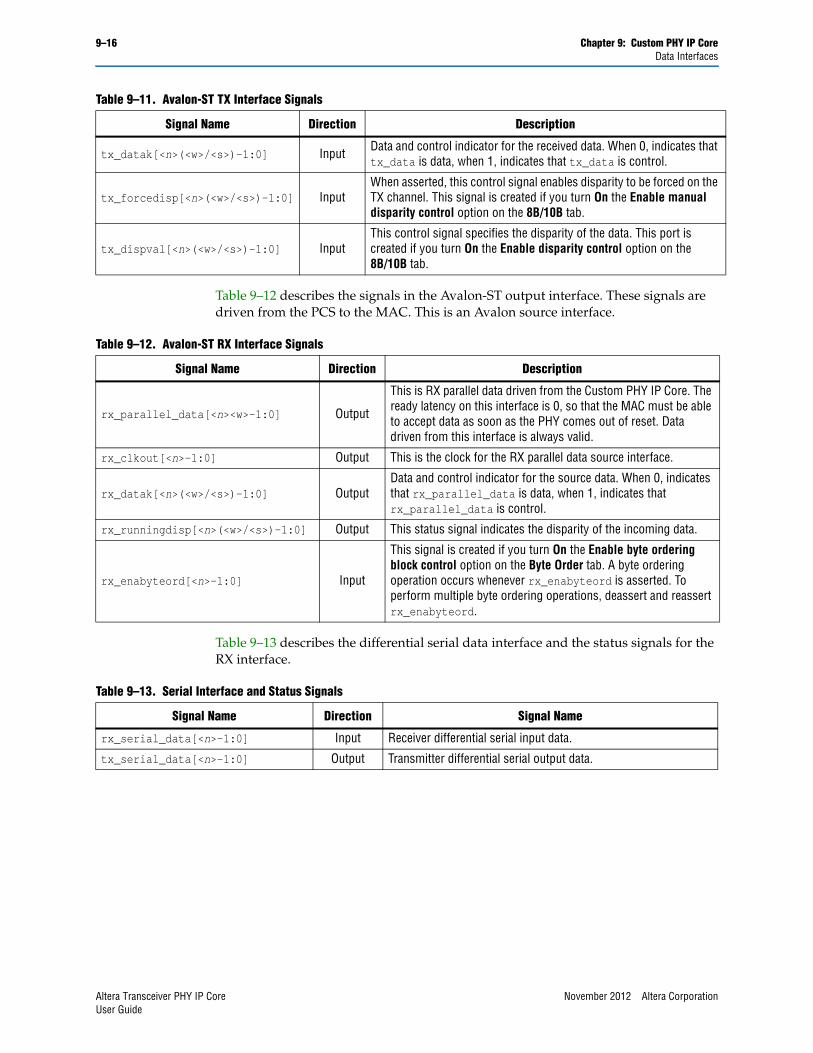
9–16 Chapter 9: Custom PHY IP CoreData Interfaces
Table 9–12 describes the signals in the Avalon-ST output interface. These signals are driven from the PCS to the MAC. This is an Avalon source interface.
Table 9–13 describes the differential serial data interface and the status signals for the RX interface.
tx_datak[<n>(<w>/<s>)-1:0] Input Data and control indicator for the received data. When 0, indicates that tx_data is data, when 1, indicates that tx_data is control.
tx_forcedisp[<n>(<w>/<s>)-1:0] InputWhen asserted, this control signal enables disparity to be forced on the TX channel. This signal is created if you turn On the Enable manual disparity control option on the 8B/10B tab.
tx_dispval[<n>(<w>/<s>)-1:0] InputThis control signal specifies the disparity of the data. This port is created if you turn On the Enable disparity control option on the 8B/10B tab.
Table 9–11. Avalon-ST TX Interface Signals
Signal Name Direction Description
Table 9–12. Avalon-ST RX Interface Signals
Signal Name Direction Description
rx_parallel_data[<n><w>-1:0] Output
This is RX parallel data driven from the Custom PHY IP Core. The ready latency on this interface is 0, so that the MAC must be able to accept data as soon as the PHY comes out of reset. Data driven from this interface is always valid.
rx_clkout[<n>-1:0] Output This is the clock for the RX parallel data source interface.
rx_datak[<n>(<w>/<s>)-1:0] OutputData and control indicator for the source data. When 0, indicates that rx_parallel_data is data, when 1, indicates that rx_parallel_data is control.
rx_runningdisp[<n>(<w>/<s>)-1:0] Output This status signal indicates the disparity of the incoming data.
rx_enabyteord[<n>-1:0] Input
This signal is created if you turn On the Enable byte ordering block control option on the Byte Order tab. A byte ordering operation occurs whenever rx_enabyteord is asserted. To perform multiple byte ordering operations, deassert and reassert rx_enabyteord.
Table 9–13. Serial Interface and Status Signals
Signal Name Direction Signal Name
rx_serial_data[<n>-1:0] Input Receiver differential serial input data.
tx_serial_data[<n>-1:0] Output Transmitter differential serial output data.
Altera Transceiver PHY IP Core November 2012 Altera CorporationUser Guide
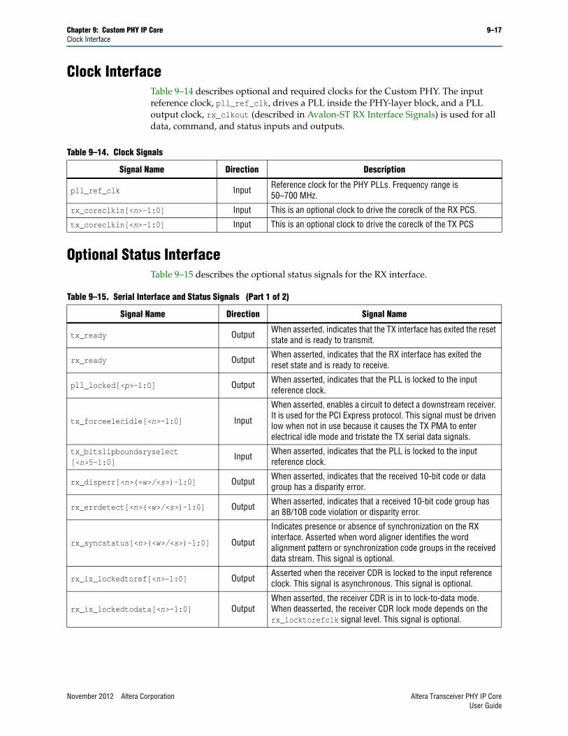
Chapter 9: Custom PHY IP Core 9–17Clock Interface
Clock InterfaceTable 9–14 describes optional and required clocks for the Custom PHY. The input reference clock, pll_ref_clk, drives a PLL inside the PHY-layer block, and a PLL output clock, rx_clkout (described in Avalon-ST RX Interface Signals) is used for all data, command, and status inputs and outputs.
Optional Status InterfaceTable 9–15 describes the optional status signals for the RX interface.
Table 9–14. Clock Signals
Signal Name Direction Description
pll_ref_clk Input Reference clock for the PHY PLLs. Frequency range is 50–700 MHz.
rx_coreclkin[<n>-1:0] Input This is an optional clock to drive the coreclk of the RX PCS.
tx_coreclkin[<n>-1:0] Input This is an optional clock to drive the coreclk of the TX PCS
Table 9–15. Serial Interface and Status Signals (Part 1 of 2)
Signal Name Direction Signal Name
tx_ready Output When asserted, indicates that the TX interface has exited the reset state and is ready to transmit.
rx_ready Output When asserted, indicates that the RX interface has exited the reset state and is ready to receive.
pll_locked[<p>-1:0] Output When asserted, indicates that the PLL is locked to the input reference clock.
tx_forceelecidle[<n>-1:0] Input
When asserted, enables a circuit to detect a downstream receiver. It is used for the PCI Express protocol. This signal must be driven low when not in use because it causes the TX PMA to enter electrical idle mode and tristate the TX serial data signals.
tx_bitslipboundaryselect[<n>5-1:0]
Input When asserted, indicates that the PLL is locked to the input reference clock.
rx_disperr[<n>(<w>/<s>)-1:0] Output When asserted, indicates that the received 10-bit code or data group has a disparity error.
rx_errdetect[<n>(<w>/<s>)-1:0] Output When asserted, indicates that a received 10-bit code group has an 8B/10B code violation or disparity error.
rx_syncstatus[<n>(<w>/<s>)-1:0] Output
Indicates presence or absence of synchronization on the RX interface. Asserted when word aligner identifies the word alignment pattern or synchronization code groups in the received data stream. This signal is optional.
rx_is_lockedtoref[<n>-1:0] Output Asserted when the receiver CDR is locked to the input reference clock. This signal is asynchronous. This signal is optional.
rx_is_lockedtodata[<n>-1:0] OutputWhen asserted, the receiver CDR is in to lock-to-data mode. When deasserted, the receiver CDR lock mode depends on the rx_locktorefclk signal level. This signal is optional.
November 2012 Altera Corporation Altera Transceiver PHY IP CoreUser Guide
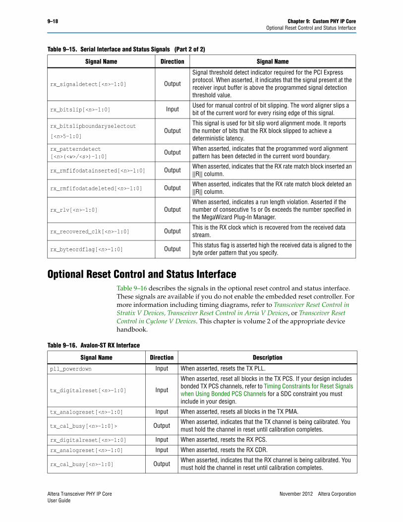
9–18 Chapter 9: Custom PHY IP CoreOptional Reset Control and Status Interface
Optional Reset Control and Status InterfaceTable 9–16 describes the signals in the optional reset control and status interface. These signals are available if you do not enable the embedded reset controller. For more information including timing diagrams, refer to Transceiver Reset Control in Stratix V Devices, Transceiver Reset Control in Arria V Devices, or Transceiver Reset Control in Cyclone V Devices. This chapter is volume 2 of the appropriate device handbook.
rx_signaldetect[<n>-1:0] Output
Signal threshold detect indicator required for the PCI Express protocol. When asserted, it indicates that the signal present at the receiver input buffer is above the programmed signal detection threshold value.
rx_bitslip[<n>-1:0] Input Used for manual control of bit slipping. The word aligner slips a bit of the current word for every rising edge of this signal.
rx_bitslipboundaryselectout
[<n>5-1:0]Output
This signal is used for bit slip word alignment mode. It reports the number of bits that the RX block slipped to achieve a deterministic latency.
rx_patterndetect[<n>(<w>/<s>)-1:0]
Output When asserted, indicates that the programmed word alignment pattern has been detected in the current word boundary.
rx_rmfifodatainserted[<n>-1:0] Output When asserted, indicates that the RX rate match block inserted an ||R|| column.
rx_rmfifodatadeleted[<n>-1:0] Output When asserted, indicates that the RX rate match block deleted an ||R|| column.
rx_rlv[<n>-1:0] OutputWhen asserted, indicates a run length violation. Asserted if the number of consecutive 1s or 0s exceeds the number specified in the MegaWizard Plug-In Manager.
rx_recovered_clk[<n>-1:0] Output This is the RX clock which is recovered from the received data stream.
rx_byteordflag[<n>-1:0] Output This status flag is asserted high the received data is aligned to the byte order pattern that you specify.
Table 9–15. Serial Interface and Status Signals (Part 2 of 2)
Signal Name Direction Signal Name
Table 9–16. Avalon-ST RX Interface
Signal Name Direction Description
pll_powerdown Input When asserted, resets the TX PLL.
tx_digitalreset[<n>-1:0] Input
When asserted, reset all blocks in the TX PCS. If your design includes bonded TX PCS channels, refer to Timing Constraints for Reset Signals when Using Bonded PCS Channels for a SDC constraint you must include in your design.
tx_analogreset[<n>-1:0] Input When asserted, resets all blocks in the TX PMA.
tx_cal_busy[<n>-1:0]> Output When asserted, indicates that the TX channel is being calibrated. You must hold the channel in reset until calibration completes.
rx_digitalreset[<n>-1:0] Input When asserted, resets the RX PCS.
rx_analogreset[<n>-1:0] Input When asserted, resets the RX CDR.
rx_cal_busy[<n>-1:0] Output When asserted, indicates that the RX channel is being calibrated. You must hold the channel in reset until calibration completes.
Altera Transceiver PHY IP Core November 2012 Altera CorporationUser Guide
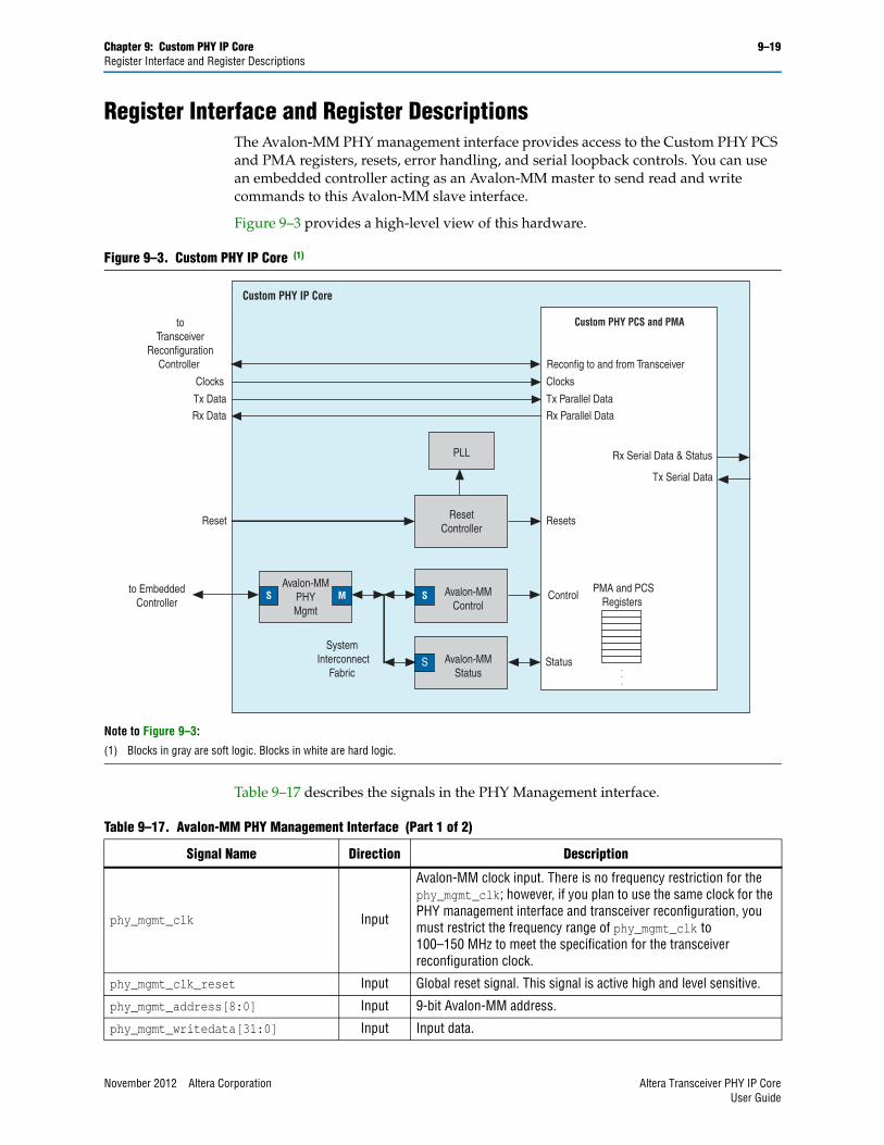
Chapter 9: Custom PHY IP Core 9–19Register Interface and Register Descriptions
Register Interface and Register DescriptionsThe Avalon-MM PHY management interface provides access to the Custom PHY PCS and PMA registers, resets, error handling, and serial loopback controls. You can use an embedded controller acting as an Avalon-MM master to send read and write commands to this Avalon-MM slave interface.
Figure 9–3 provides a high-level view of this hardware.
Table 9–17 describes the signals in the PHY Management interface.
Figure 9–3. Custom PHY IP Core (1)
Note to Figure 9–3:
(1) Blocks in gray are soft logic. Blocks in white are hard logic.
System Interconnect
Fabric
to EmbeddedController
Custom PHY PCS and PMA
Custom PHY IP Core
Resets
Status
ControlS Avalon-MMControl
S Avalon-MMStatus
ResetController
PLL
Reset
Clocks Clocks
toTransceiver
ReconfigurationController
Tx Data Tx Parallel Data Rx Data Rx Parallel Data
MAvalon-MM
PHYMgmt
S
Rx Serial Data & Status
Reconfig to and from Transceiver
Tx Serial Data
PMA and PCSRegisters
.
.
.
Table 9–17. Avalon-MM PHY Management Interface (Part 1 of 2)
Signal Name Direction Description
phy_mgmt_clk Input
Avalon-MM clock input. There is no frequency restriction for the phy_mgmt_clk; however, if you plan to use the same clock for the PHY management interface and transceiver reconfiguration, you must restrict the frequency range of phy_mgmt_clk to 100–150 MHz to meet the specification for the transceiver reconfiguration clock.
phy_mgmt_clk_reset Input Global reset signal. This signal is active high and level sensitive.
phy_mgmt_address[8:0] Input 9-bit Avalon-MM address.
phy_mgmt_writedata[31:0] Input Input data.
November 2012 Altera Corporation Altera Transceiver PHY IP CoreUser Guide
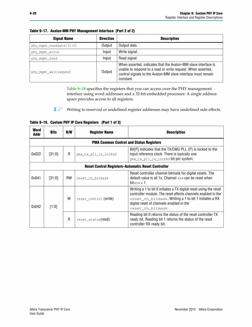
9–20 Chapter 9: Custom PHY IP CoreRegister Interface and Register Descriptions
Table 9–18 specifies the registers that you can access over the PHY management interface using word addresses and a 32-bit embedded processor. A single address space provides access to all registers.
1 Writing to reserved or undefined register addresses may have undefined side effects.
phy_mgmt_readdata[31:0] Output Output data.
phy_mgmt_write Input Write signal.
phy_mgmt_read Input Read signal.
phy_mgmt_waitrequest Output
When asserted, indicates that the Avalon-MM slave interface is unable to respond to a read or write request. When asserted, control signals to the Avalon-MM slave interface must remain constant.
Table 9–17. Avalon-MM PHY Management Interface (Part 2 of 2)
Signal Name Direction Description
Table 9–18. Custom PHY IP Core Registers (Part 1 of 3)
Word Addr Bits R/W Register Name Description
PMA Common Control and Status Registers
0x022 [31:0] R pma_tx_pll_is_lockedBit[P] indicates that the TX/CMU PLL (P) is locked to the input reference clock. There is typically one pma_tx_pll_is_locked bit per system.
Reset Control Registers–Automatic Reset Controller
0x041 [31:0] RW reset_ch_bitmaskReset controller channel bitmask for digital resets. The default value is all 1s. Channel <n> can be reset when bit<n> = 1.
0x042 [1:0]
W reset_control (write)
Writing a 1 to bit 0 initiates a TX digital reset using the reset controller module. The reset affects channels enabled in the reset_ch_bitmask. Writing a 1 to bit 1 initiates a RX digital reset of channels enabled in the reset_ch_bitmask.
R reset_status(read)Reading bit 0 returns the status of the reset controller TX ready bit. Reading bit 1 returns the status of the reset controller RX ready bit.
Altera Transceiver PHY IP Core November 2012 Altera CorporationUser Guide
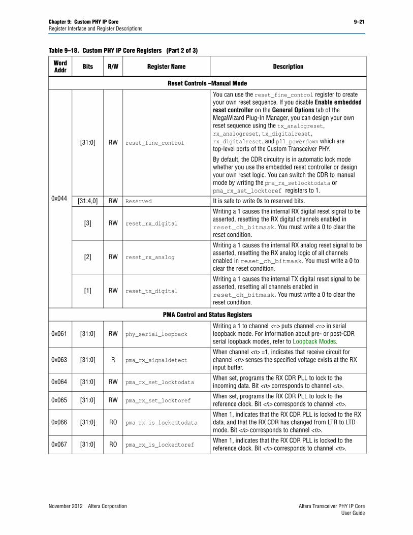
Chapter 9: Custom PHY IP Core 9–21Register Interface and Register Descriptions
Reset Controls –Manual Mode
0x044
[31:0] RW reset_fine_control
You can use the reset_fine_control register to create your own reset sequence. If you disable Enable embedded reset controller on the General Options tab of the MegaWizard Plug-In Manager, you can design your own reset sequence using the tx_analogreset, rx_analogreset, tx_digitalreset, rx_digitalreset, and pll_powerdown which are top-level ports of the Custom Transceiver PHY.
By default, the CDR circuitry is in automatic lock mode whether you use the embedded reset controller or design your own reset logic. You can switch the CDR to manual mode by writing the pma_rx_setlocktodata or pma_rx_set_locktoref registers to 1.
[31:4,0] RW Reserved It is safe to write 0s to reserved bits.
[3] RW reset_rx_digital
Writing a 1 causes the internal RX digital reset signal to be asserted, resetting the RX digital channels enabled in reset_ch_bitmask. You must write a 0 to clear the reset condition.
[2] RW reset_rx_analog
Writing a 1 causes the internal RX analog reset signal to be asserted, resetting the RX analog logic of all channels enabled in reset_ch_bitmask. You must write a 0 to clear the reset condition.
[1] RW reset_tx_digital
Writing a 1 causes the internal TX digital reset signal to be asserted, resetting all channels enabled in reset_ch_bitmask. You must write a 0 to clear the reset condition.
PMA Control and Status Registers
0x061 [31:0] RW phy_serial_loopbackWriting a 1 to channel <n> puts channel <n> in serial loopback mode. For information about pre- or post-CDR serial loopback modes, refer to Loopback Modes.
0x063 [31:0] R pma_rx_signaldetectWhen channel <n> =1, indicates that receive circuit for channel <n> senses the specified voltage exists at the RX input buffer.
0x064 [31:0] RW pma_rx_set_locktodataWhen set, programs the RX CDR PLL to lock to the incoming data. Bit <n> corresponds to channel <n>.
0x065 [31:0] RW pma_rx_set_locktorefWhen set, programs the RX CDR PLL to lock to the reference clock. Bit <n> corresponds to channel <n>.
0x066 [31:0] RO pma_rx_is_lockedtodataWhen 1, indicates that the RX CDR PLL is locked to the RX data, and that the RX CDR has changed from LTR to LTD mode. Bit <n> corresponds to channel <n>.
0x067 [31:0] RO pma_rx_is_lockedtorefWhen 1, indicates that the RX CDR PLL is locked to the reference clock. Bit <n> corresponds to channel <n>.
Table 9–18. Custom PHY IP Core Registers (Part 2 of 3)
Word Addr Bits R/W Register Name Description
November 2012 Altera Corporation Altera Transceiver PHY IP CoreUser Guide
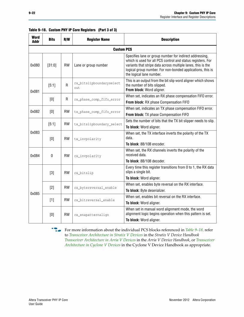
9–22 Chapter 9: Custom PHY IP CoreRegister Interface and Register Descriptions
f For more information about the individual PCS blocks referenced in Table 9–18, refer to Transceiver Architecture in Stratix V Devices in the Stratix V Device Handbook Transceiver Architecture in Arria V Devices in the Arria V Device Handbook, or Transceiver Architecture in Cyclone V Devices in the Cyclone V Device Handbook as appropriate.
Custom PCS
0x080 [31:0] RW Lane or group number
Specifies lane or group number for indirect addressing, which is used for all PCS control and status registers. For variants that stripe data across multiple lanes, this is the logical group number. For non-bonded applications, this is the logical lane number.
0x081
[5:1] R rx_bitslipboundaryselectout
This is an output from the bit slip word aligner which shows the number of bits slipped.From block: Word aligner.
[0] R rx_phase_comp_fifo_errorWhen set, indicates an RX phase compensation FIFO error.
From block: RX phase Compensation FIFO
0x082 [0] RW tx_phase_comp_fifo_errorWhen set, indicates an TX phase compensation FIFO error.
From block: TX phase Compensation FIFO
0x083
[5:1] RW tx_bitslipboundary_selectSets the number of bits that the TX bit slipper needs to slip.
To block: Word aligner.
[0] RW tx_invpolarity
When set, the TX interface inverts the polarity of the TX data.
To block: 8B/10B encoder.
0x084 0 RW rx_invpolarity
When set, the RX channels inverts the polarity of the received data.
To block: 8B/10B decoder.
0x085
[3] RW rx_bitslip
Every time this register transitions from 0 to 1, the RX data slips a single bit.
To block: Word aligner.
[2] RW rx_bytereversal_enableWhen set, enables byte reversal on the RX interface.
To block: Byte deserializer.
[1] RW rx_bitreversal_enableWhen set, enables bit reversal on the RX interface.
To block: Word aligner.
[0] RW rx_enapatternalign
When set in manual word alignment mode, the word alignment logic begins operation when this pattern is set.
To block: Word aligner.
Table 9–18. Custom PHY IP Core Registers (Part 3 of 3)
Word Addr Bits R/W Register Name Description
Altera Transceiver PHY IP Core November 2012 Altera CorporationUser Guide
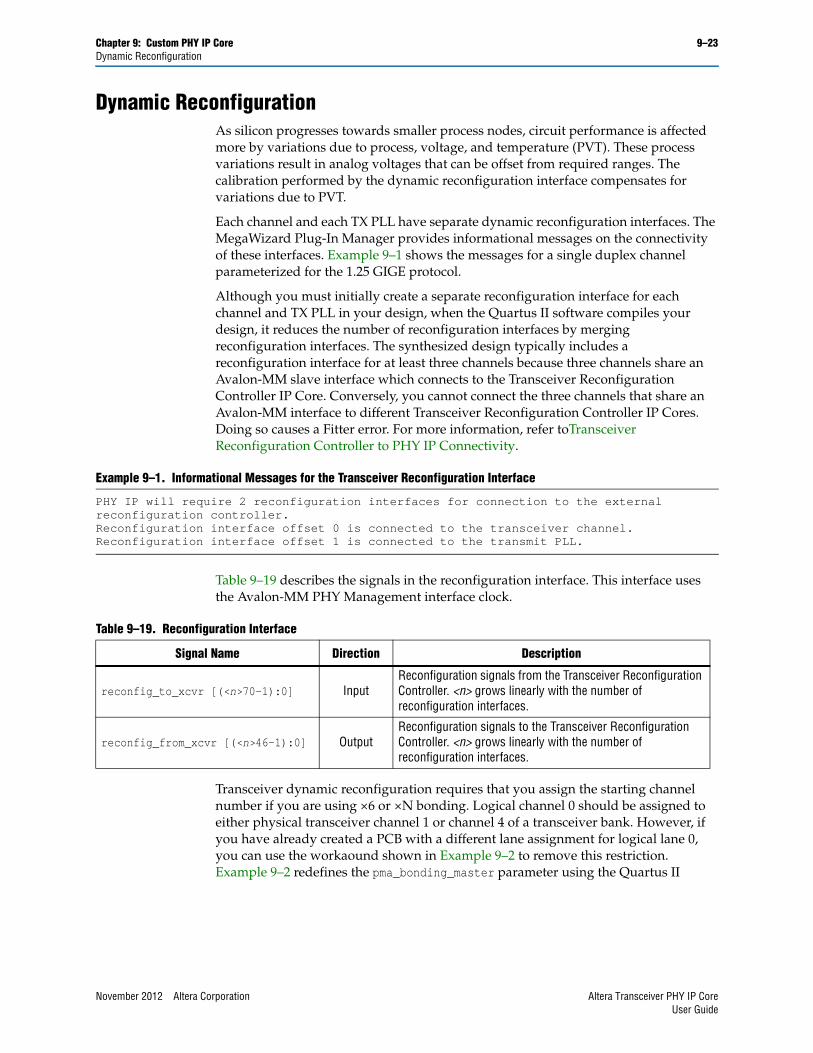
Chapter 9: Custom PHY IP Core 9–23Dynamic Reconfiguration
Dynamic ReconfigurationAs silicon progresses towards smaller process nodes, circuit performance is affected more by variations due to process, voltage, and temperature (PVT). These process variations result in analog voltages that can be offset from required ranges. The calibration performed by the dynamic reconfiguration interface compensates for variations due to PVT.
Each channel and each TX PLL have separate dynamic reconfiguration interfaces. The MegaWizard Plug-In Manager provides informational messages on the connectivity of these interfaces. Example 9–1 shows the messages for a single duplex channel parameterized for the 1.25 GIGE protocol.
Although you must initially create a separate reconfiguration interface for each channel and TX PLL in your design, when the Quartus II software compiles your design, it reduces the number of reconfiguration interfaces by merging reconfiguration interfaces. The synthesized design typically includes a reconfiguration interface for at least three channels because three channels share an Avalon-MM slave interface which connects to the Transceiver Reconfiguration Controller IP Core. Conversely, you cannot connect the three channels that share an Avalon-MM interface to different Transceiver Reconfiguration Controller IP Cores. Doing so causes a Fitter error. For more information, refer toTransceiver Reconfiguration Controller to PHY IP Connectivity.
Table 9–19 describes the signals in the reconfiguration interface. This interface uses the Avalon-MM PHY Management interface clock.
Transceiver dynamic reconfiguration requires that you assign the starting channel number if you are using ×6 or ×N bonding. Logical channel 0 should be assigned to either physical transceiver channel 1 or channel 4 of a transceiver bank. However, if you have already created a PCB with a different lane assignment for logical lane 0, you can use the workaound shown in Example 9–2 to remove this restriction. Example 9–2 redefines the pma_bonding_master parameter using the Quartus II
Example 9–1. Informational Messages for the Transceiver Reconfiguration Interface
PHY IP will require 2 reconfiguration interfaces for connection to the external reconfiguration controller.Reconfiguration interface offset 0 is connected to the transceiver channel.Reconfiguration interface offset 1 is connected to the transmit PLL.
Table 9–19. Reconfiguration Interface
Signal Name Direction Description
reconfig_to_xcvr [(<n>70-1):0] InputReconfiguration signals from the Transceiver Reconfiguration Controller. <n> grows linearly with the number of reconfiguration interfaces.
reconfig_from_xcvr [(<n>46-1):0] OutputReconfiguration signals to the Transceiver Reconfiguration Controller. <n> grows linearly with the number of reconfiguration interfaces.
November 2012 Altera Corporation Altera Transceiver PHY IP CoreUser Guide
9–24 Chapter 9: Custom PHY IP CoreSimulation Files and Example Testbench
Assignment Editor. In this example, the pma_bonding_master was originally assigned to physical channel 1. (The original assignment could also have been to physical channel 4.) The to parameter reassigns the pma_bonding_master to the Custom PHY instance name. You must substitute the instance name from your design for the instance name shown in quotation marks
Simulation Files and Example Testbench Refer to Running a Simulation Testbench for a description of the directories and files that the Quartus II software creates automatically when you generate your Custom PHY IP Core.
f Refer to the Altera wiki for an example testbench that you can use as a starting point in creating your own verification environment.
Example 9–2. Overriding Logical Channel 0 Channel Assignment Restrictions in Stratix V Devices for ×6 or ×N Bonding
set_parameter -name pma_bonding_master "\"1\"" -to "<custom phy instance>|altera_xcvr_custom:my_custom_phy_inst|sv_xcvr_custom_nr:S5|sv_xcvr_custom_native:transceiver_core|sv_xcvr_native:gen.sv_xcvr_native_insts[0].gen_bonded_group.sv_xcvr_native_inst"
Altera Transceiver PHY IP Core November 2012 Altera CorporationUser Guide
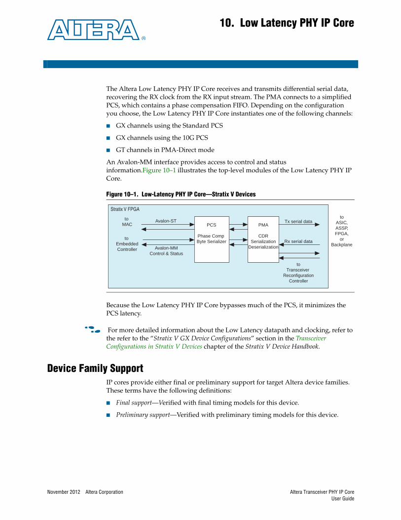
November 2012 Altera Corporation
10. Low Latency PHY IP Core
The Altera Low Latency PHY IP Core receives and transmits differential serial data, recovering the RX clock from the RX input stream. The PMA connects to a simplified PCS, which contains a phase compensation FIFO. Depending on the configuration you choose, the Low Latency PHY IP Core instantiates one of the following channels:
■ GX channels using the Standard PCS
■ GX channels using the 10G PCS
■ GT channels in PMA-Direct mode
An Avalon-MM interface provides access to control and status information.Figure 10–1 illustrates the top-level modules of the Low Latency PHY IP Core.
Because the Low Latency PHY IP Core bypasses much of the PCS, it minimizes the PCS latency.
f For more detailed information about the Low Latency datapath and clocking, refer to the refer to the “Stratix V GX Device Configurations” section in the Transceiver Configurations in Stratix V Devices chapter of the Stratix V Device Handbook.
Device Family SupportIP cores provide either final or preliminary support for target Altera device families. These terms have the following definitions:
■ Final support—Verified with final timing models for this device.
■ Preliminary support—Verified with preliminary timing models for this device.
Figure 10–1. Low-Latency PHY IP Core—Stratix V Devices
Tx serial data
Rx serial data
Stratix V FPGA
PMA
CDRSerialization
Deserialization
PCS
Phase Comp Byte Serializer
Avalon-MMControl & Status
Avalon-STto MAC
to EmbeddedController
toTransceiver
ReconfigurationController
toASIC,ASSP,FPGA,
orBackplane
Altera Transceiver PHY IP CoreUser Guide
10–2 Chapter 10: Low Latency PHY IP CorePerformance and Resource Utilization - Need Update
Table 10–1 shows the level of support offered by the Low Latency PHY IP Core for Altera device families.
Performance and Resource Utilization - Need UpdateTable 10–2 shows the typical expected device resource utilization for different configurations using the current version of the Quartus II software targeting a Stratix V GX (5SGSMD612H35C2) device. .
Parameterizing the Low Latency PHYComplete the following steps to configure the Low Latency PHY IP Core in the MegaWizard Plug-In Manager:
Table 10–1. Device Family Support
Device Family Support
Stratix V devices Preliminary
Other device families No support
Table 10–2. Low Latency PHY Performance and Resource Utilization—Stratix V GX Device
Implementation Number of Lanes
Serialization Factor
Worst-Case Frequency
Combinational ALUTs
DedicatedRegisters
Memory Bits
11 Gbps 1 32 or 40 599.16 112 95 0
11 Gbps 4 32 or 40 584.8 141 117 0
11 Gbps 10 32 or 40 579.71 192 171 0
6 Gbps (10 Gbps datapath) 1 32 or 40 608.27 111 93 0
6 Gbps (10 Gbps datapath) 4 32 or 40 454.96 141 117 0
6 Gbps (10 Gbps datapath) 10 32 or 40 562.75 192 171 0
6 Gbps (8 Gbps datapath) 1 32 or 40 607.16 113 93 0
6 Gbps (8 Gbps datapath) 4 32 or 40 639.8 142 117 0
6 Gbps (8 Gbps datapath) 10 32 or 40 621.89 193 171 0
3 Gbps (8 Gbps datapath) 1 8, 10, 16, or 20 673.4 114 93 0
3 Gbps (8 Gbps datapath) 4 8, 10, 16, or 20 594.88 142 117 0
3 Gbps (8 Gbps datapath) 10 8, 10, 16, or 20 667.67 193 171 0
Altera Transceiver PHY IP Core November 2012 Altera CorporationUser Guide
Chapter 10: Low Latency PHY IP Core 10–3General Options Parameters
1. For Which device family will you be using?, select Stratix V.
2. Click Installed Plug-Ins > Interfaces > Transceiver PHY >Low Latency PHY v12.1.
3. Use the tabs on the MegaWizard Plug-In Manager to select the options required for the protocol.
4. Refer to the following topics to learn more about the parameters:
a. General Options Parameters
b. Additional Options Parameters
c. PLL Reconfiguration Parameters
d. Analog Parameters
5. Click Finish to generate your parameterized Low Latency PHY IP Core.
General Options ParametersTable 10–3 lists the settings available on General Options tab.
Table 10–3. Low Latency PHY General Options
Name Value Description
Device family Stratix V This IP core is only available for Stratix V devices.
Datapath typeStandard
10GGT
The Low Latency PHY IP Core is part of a Standard, 10G, or GT datapath. In most cases the FPGA fabric transceiver interface width determines the bandwidth of the datapath; however, when the FPGA fabric transceiver interface width is 32 or 40 bits, you have the option of using either the Standard datapath which is the default mode, or changing to the 10G datapath by selecting this option. Refer to Table 10–4 for a comprehensive list of datapath support.
Mode of operationDuplex
RXTX
Specifies the mode of operation as Duplex, RX, or TX mode.
Number of lanes 1-32
Specifies the total number of lanes in each direction. Stratix V devices include up to 32 GX channels (Standard or 10G) and up to 4 GT channels. You must instantiate each GT channel in a separate Low Latency PHY IP Core instance. You cannot specify both GX and GT channels within the same instance.
Enable lane bonding On/Off
When enabled, the PMA uses the same clock source for up to 6 channels in a transceiver bank, reducing clock skew.
Turn this option Off if you are using multiple TX PLLs in a single Low Latency PHY IP Core instance.
November 2012 Altera Corporation Altera Transceiver PHY IP CoreUser Guide
10–4 Chapter 10: Low Latency PHY IP CoreGeneral Options Parameters
Bonding mode ×Nfb_compensation
Select ×N to use the same clock source for up to 6 channels in a single transceiver bank, resulting in reduced clock skew. You must use contiguous channels when you select ×N bonding. In addition, you must place logical channel 0 in either physical channel 1 or 4. Physical channels 1 and 4 are indirect drivers of the ×N clock network.
Select fb_compensation (feedback compensation) to use the same clock source for multiple channels across different transceiver banks to reduce clock skew.
For more information about bonding, refer to “Bonded Channel Configurations Using the PLL Feedback Compensation Path” in Transceiver Clocking in Stratix V Devices in volume 2 of the Stratix V Device Handbook.
FPGA fabric transceiver interface width
8, 10, 16, 20, 32, 40, 50, 64, 66, 128
This option indicates the parallel data fabric transceiver interface width. GT datapath supports a single width of 128 bits. Refer toTable 10–4 for the supported interface widths of the Standard and 10G datapaths.
PCS-PMA interface width 8, 10, 16, 20, 32, 30, 64
The PCS-PMA interface width depends on the FPGA fabric transceiver interface width and the Datapath type. Refer to Table 10–4 for the supported interface widths of the Standard and 10G datapaths.
PLL type CMUATX
The CMU PLL is available for the Standard and 10G datapaths. The ATX PLL is available for the Standard, 10G, and GT datapaths. The CMU PLL has a larger frequency range than the ATX PLL. The ATX PLL is designed to improve jitter performance and achieves lower channel-to-channel skew; however, it supports a narrower range of data rates and reference clock frequencies. Another advantage of the ATX PLL is that it does not use a transceiver channel, while the CMU PLL does.
An informational message displays in the message panel if the PLL type that you select is not available at the frequency specified.
Data rate Device dependent Specifies the data rate in Mbps. Refer to Stratix V Device Datasheet for the data rate ranges of datapath.
Base data rate1 × Data rate2 × Data rate4 × Data rate
Select a base data rate that minimizes the number of PLLs required to generate all the clocks required for data transmission. By selecting an appropriate base data rate, you can change data rates by changing the divider used by the clock generation block. For higher frequency data rates 2 × and 4× base data rates are not available.
Input clock frequency Variable
Specifies the frequency of the PLL input reference clock. The Input clock frequency drop down menu is populated with all valid frequencies derived as a function of the data rate and base data rate. However, if you select fb_compensation as the bonding mode, then the input reference clock frequency is limited to the (data rate) (PCS-PMA interface width).
Table 10–3. Low Latency PHY General Options
Name Value Description
Altera Transceiver PHY IP Core November 2012 Altera CorporationUser Guide
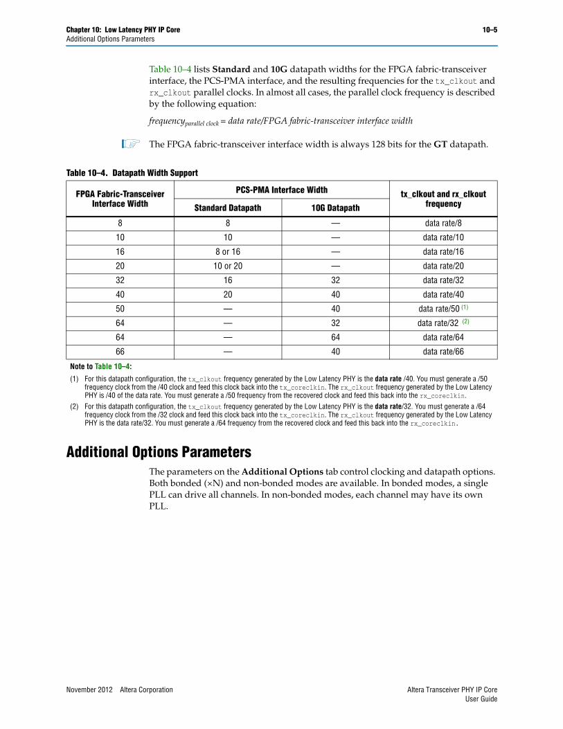
Chapter 10: Low Latency PHY IP Core 10–5Additional Options Parameters
Table 10–4 lists Standard and 10G datapath widths for the FPGA fabric-transceiver interface, the PCS-PMA interface, and the resulting frequencies for the tx_clkout and rx_clkout parallel clocks. In almost all cases, the parallel clock frequency is described by the following equation:
frequencyparallel clock = data rate/FPGA fabric-transceiver interface width
1 The FPGA fabric-transceiver interface width is always 128 bits for the GT datapath.
Additional Options ParametersThe parameters on the Additional Options tab control clocking and datapath options. Both bonded (×N) and non-bonded modes are available. In bonded modes, a single PLL can drive all channels. In non-bonded modes, each channel may have its own PLL.
Table 10–4. Datapath Width Support
FPGA Fabric-Transceiver Interface Width
PCS-PMA Interface Width tx_clkout and rx_clkout frequencyStandard Datapath 10G Datapath
8 8 — data rate/8
10 10 — data rate/10
16 8 or 16 — data rate/16
20 10 or 20 — data rate/20
32 16 32 data rate/32
40 20 40 data rate/40
50 — 40 data rate/50 (1)
64 — 32 data rate/32 (2)
64 — 64 data rate/64
66 — 40 data rate/66
Note to Table 10–4:
(1) For this datapath configuration, the tx_clkout frequency generated by the Low Latency PHY is the data rate /40. You must generate a /50 frequency clock from the /40 clock and feed this clock back into the tx_coreclkin. The rx_clkout frequency generated by the Low Latency PHY is /40 of the data rate. You must generate a /50 frequency from the recovered clock and feed this back into the rx_coreclkin.
(2) For this datapath configuration, the tx_clkout frequency generated by the Low Latency PHY is the data rate/32. You must generate a /64 frequency clock from the /32 clock and feed this clock back into the tx_coreclkin. The rx_clkout frequency generated by the Low Latency PHY is the data rate/32. You must generate a /64 frequency from the recovered clock and feed this back into the rx_coreclkin.
November 2012 Altera Corporation Altera Transceiver PHY IP CoreUser Guide
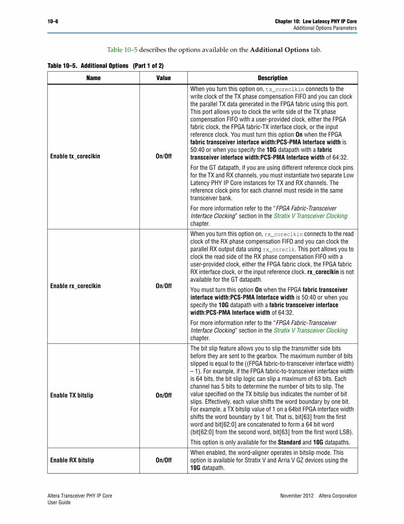
10–6 Chapter 10: Low Latency PHY IP CoreAdditional Options Parameters
Table 10–5 describes the options available on the Additional Options tab.
Table 10–5. Additional Options (Part 1 of 2)
Name Value Description
Enable tx_coreclkin On/Off
When you turn this option on, tx_coreclkin connects to the write clock of the TX phase compensation FIFO and you can clock the parallel TX data generated in the FPGA fabric using this port. This port allows you to clock the write side of the TX phase compensation FIFO with a user-provided clock, either the FPGA fabric clock, the FPGA fabric-TX interface clock, or the input reference clock. You must turn this option On when the FPGA fabric transceiver interface width:PCS-PMA Interface width is 50:40 or when you specify the 10G datapath with a fabric transceiver interface width:PCS-PMA Interface width of 64:32.
For the GT datapath, if you are using different reference clock pins for the TX and RX channels, you must instantiate two separate Low Latency PHY IP Core instances for TX and RX channels. The reference clock pins for each channel must reside in the same transceiver bank.
For more information refer to the “FPGA Fabric-Transceiver Interface Clocking” section in the Stratix V Transceiver Clocking chapter.
Enable rx_coreclkin On/Off
When you turn this option on, rx_coreclkin connects to the read clock of the RX phase compensation FIFO and you can clock the parallel RX output data using rx_coreclk. This port allows you to clock the read side of the RX phase compensation FIFO with a user-provided clock, either the FPGA fabric clock, the FPGA fabric RX interface clock, or the input reference clock. rx_coreclkin is not available for the GT datapath.
You must turn this option On when the FPGA fabric transceiver interface width:PCS-PMA Interface width is 50:40 or when you specify the 10G datapath with a fabric transceiver interface width:PCS-PMA Interface width of 64:32.
For more information refer to the “FPGA Fabric-Transceiver Interface Clocking” section in the Stratix V Transceiver Clocking chapter.
Enable TX bitslip On/Off
The bit slip feature allows you to slip the transmitter side bits before they are sent to the gearbox. The maximum number of bits slipped is equal to the ((FPGA fabric-to-transceiver interface width) – 1). For example, if the FPGA fabric-to-transceiver interface width is 64 bits, the bit slip logic can slip a maximum of 63 bits. Each channel has 5 bits to determine the number of bits to slip. The value specified on the TX bitslip bus indicates the number of bit slips. Effectively, each value shifts the word boundary by one bit. For example, a TX bitslip value of 1 on a 64bit FPGA interface width shifts the word boundary by 1 bit. That is, bit[63] from the first word and bit[62:0] are concatenated to form a 64 bit word (bit[62:0] from the second word, bit[63] from the first word LSB).
This option is only available for the Standard and 10G datapaths.
Enable RX bitslip On/OffWhen enabled, the word-aligner operates in bitslip mode. This option is available for Stratix V and Arria V GZ devices using the 10G datapath.
Altera Transceiver PHY IP Core November 2012 Altera CorporationUser Guide
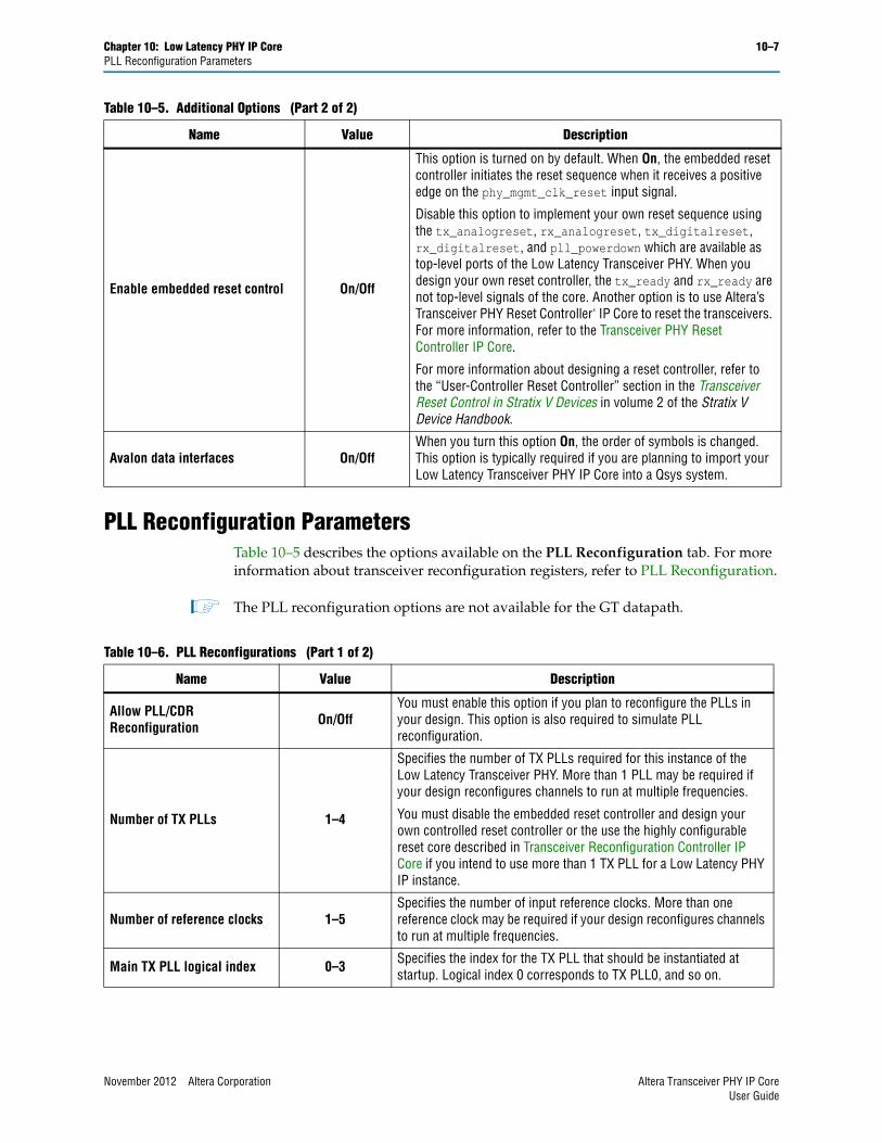
Chapter 10: Low Latency PHY IP Core 10–7PLL Reconfiguration Parameters
PLL Reconfiguration ParametersTable 10–5 describes the options available on the PLL Reconfiguration tab. For more information about transceiver reconfiguration registers, refer to PLL Reconfiguration.
1 The PLL reconfiguration options are not available for the GT datapath.
Enable embedded reset control On/Off
This option is turned on by default. When On, the embedded reset controller initiates the reset sequence when it receives a positive edge on the phy_mgmt_clk_reset input signal.
Disable this option to implement your own reset sequence using the tx_analogreset, rx_analogreset, tx_digitalreset, rx_digitalreset, and pll_powerdown which are available as top-level ports of the Low Latency Transceiver PHY. When you design your own reset controller, the tx_ready and rx_ready are not top-level signals of the core. Another option is to use Altera’s Transceiver PHY Reset Controller' IP Core to reset the transceivers. For more information, refer to the Transceiver PHY Reset Controller IP Core.
For more information about designing a reset controller, refer to the “User-Controller Reset Controller” section in the Transceiver Reset Control in Stratix V Devices in volume 2 of the Stratix V Device Handbook.
Avalon data interfaces On/OffWhen you turn this option On, the order of symbols is changed. This option is typically required if you are planning to import your Low Latency Transceiver PHY IP Core into a Qsys system.
Table 10–5. Additional Options (Part 2 of 2)
Name Value Description
Table 10–6. PLL Reconfigurations (Part 1 of 2)
Name Value Description
Allow PLL/CDR Reconfiguration On/Off
You must enable this option if you plan to reconfigure the PLLs in your design. This option is also required to simulate PLL reconfiguration.
Number of TX PLLs 1–4
Specifies the number of TX PLLs required for this instance of the Low Latency Transceiver PHY. More than 1 PLL may be required if your design reconfigures channels to run at multiple frequencies.
You must disable the embedded reset controller and design your own controlled reset controller or the use the highly configurable reset core described in Transceiver Reconfiguration Controller IP Core if you intend to use more than 1 TX PLL for a Low Latency PHY IP instance.
Number of reference clocks 1–5Specifies the number of input reference clocks. More than one reference clock may be required if your design reconfigures channels to run at multiple frequencies.
Main TX PLL logical index 0–3 Specifies the index for the TX PLL that should be instantiated at startup. Logical index 0 corresponds to TX PLL0, and so on.
November 2012 Altera Corporation Altera Transceiver PHY IP CoreUser Guide
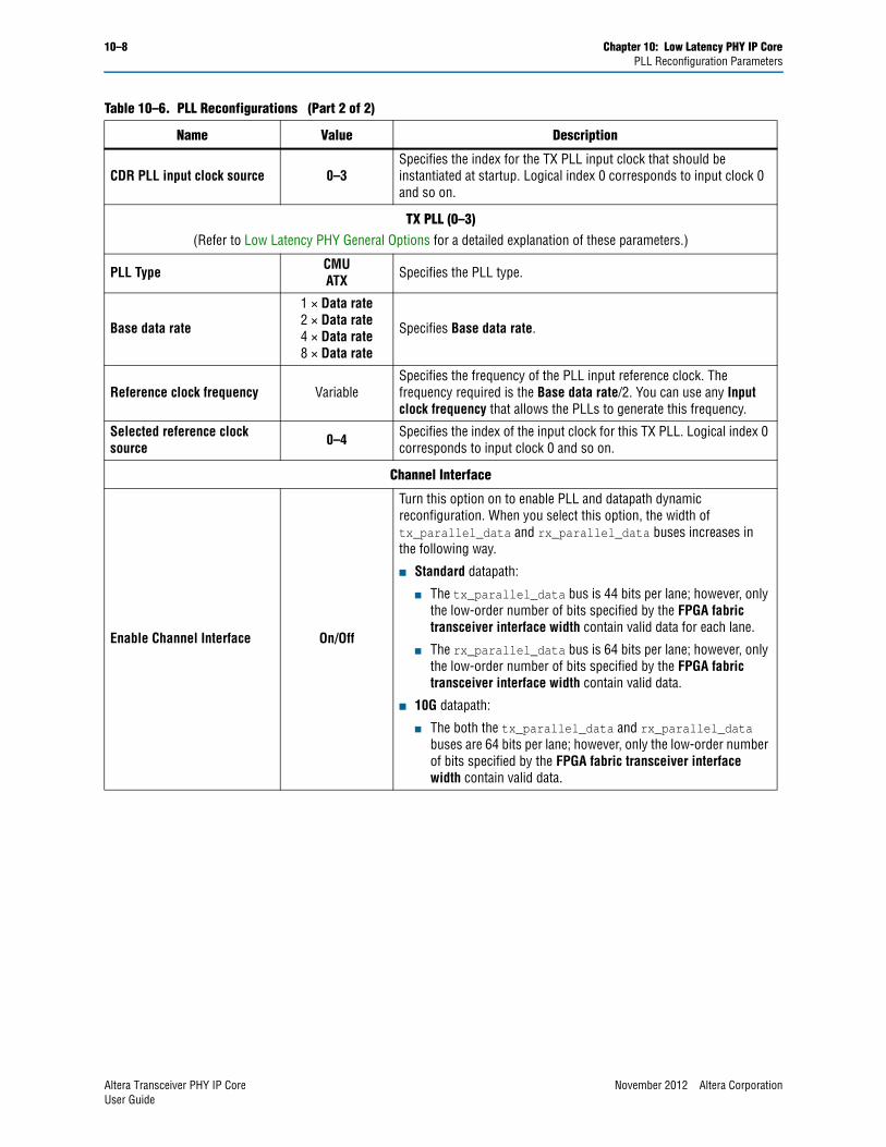
10–8 Chapter 10: Low Latency PHY IP CorePLL Reconfiguration Parameters
CDR PLL input clock source 0–3Specifies the index for the TX PLL input clock that should be instantiated at startup. Logical index 0 corresponds to input clock 0 and so on.
TX PLL (0–3)(Refer to Low Latency PHY General Options for a detailed explanation of these parameters.)
PLL Type CMUATX Specifies the PLL type.
Base data rate
1 × Data rate2 × Data rate4 × Data rate8 × Data rate
Specifies Base data rate.
Reference clock frequency VariableSpecifies the frequency of the PLL input reference clock. The frequency required is the Base data rate/2. You can use any Input clock frequency that allows the PLLs to generate this frequency.
Selected reference clock source 0–4 Specifies the index of the input clock for this TX PLL. Logical index 0
corresponds to input clock 0 and so on.
Channel Interface
Enable Channel Interface On/Off
Turn this option on to enable PLL and datapath dynamic reconfiguration. When you select this option, the width of tx_parallel_data and rx_parallel_data buses increases in the following way.
■ Standard datapath:
■ The tx_parallel_data bus is 44 bits per lane; however, only the low-order number of bits specified by the FPGA fabric transceiver interface width contain valid data for each lane.
■ The rx_parallel_data bus is 64 bits per lane; however, only the low-order number of bits specified by the FPGA fabric transceiver interface width contain valid data.
■ 10G datapath:
■ The both the tx_parallel_data and rx_parallel_data buses are 64 bits per lane; however, only the low-order number of bits specified by the FPGA fabric transceiver interface width contain valid data.
Table 10–6. PLL Reconfigurations (Part 2 of 2)
Name Value Description
Altera Transceiver PHY IP Core November 2012 Altera CorporationUser Guide
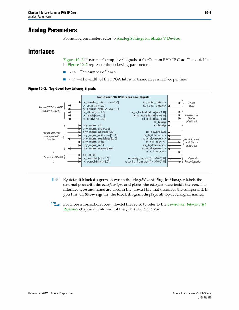
Chapter 10: Low Latency PHY IP Core 10–9Analog Parameters
Analog ParametersFor analog parameters refer to Analog Settings for Stratix V Devices.
InterfacesFigure 10–2 illustrates the top-level signals of the Custom PHY IP Core. The variables in Figure 10–2 represent the following parameters:
■ <n>—The number of lanes
■ <w>—The width of the FPGA fabric to transceiver interface per lane
1 By default block diagram shown in the MegaWizard Plug-In Manager labels the external pins with the interface type and places the interface name inside the box. The interface type and name are used in the _hw.tcl file that describes the component. If you turn on Show signals, the block diagram displays all top-level signal names.
f For more information about _hw.tcl files refer to refer to the Component Interface Tcl Reference chapter in volume 1 of the Quartus II Handbook.
Figure 10–2. Top-Level Low Latency Signals
Low Latency PHY IP Core Top-Level Signals
tx_serial_data<n>rx_serial_data<n>
rx_is_lockedtodata[<n>-1:0]rx_is_lockedtoref[<n>-1:0]
pll_locked[<n>-1:0]tx_bitsliprx_bitslip
pll_powerdowntx_digitalreset<n>
tx_analogreset<n>tx_cal_busy<n>
rx_digitalreset<n>rx_analogreset<n>
rx_cal_busy<n>
reconfig_to_xcvr[(<n>70-1):0]reconfig_from_xcvr[(<n>46-1):0]
Control andStatus
(Optional)
tx_parallel_data[<n><w>-1:0]tx_clkout[<n>-1:0]rx_parallel_data[<n><w>-1:0]rx_clkout[<n>-1:0]tx_ready[<n>-1:0] rx_ready[<n>-1:0]
phy_mgmt_clkphy_mgmt_clk_resetphy_mgmt_address[8:0]phy_mgmt_writedata[31:0]phy_mgmt_readdata[31:0]phy_mgmt_writephy_mgmt_readphy_mgmt_waitrequest
pll_ref_clktx_coreclkin[<n>-1:0]rx_coreclkin[<n>-1:0]
Avalon-MM PHYManagement
Interface
Avalon-ST TX and RX to and from MAC
SerialData
DynamicReconfiguration
Reset Controland Status(Optional)
Clocks Optional
November 2012 Altera Corporation Altera Transceiver PHY IP CoreUser Guide
10–10 Chapter 10: Low Latency PHY IP CoreData Interfaces
Data InterfacesTable 10–7 describes the signals in the Avalon-ST interface. This interface drives Avalon-ST TX and RX data to and from the FPGA fabric. These signals are named from the point of view of the MAC so that the TX interface is an Avalon-ST sink interface and the RX interface is an Avalon-ST source.
Table 10–8 describes the signals that comprise the serial data interface.
Table 10–7. Avalon-ST interface
Signal Name Direction Description
tx_parallel_data[<n><w>-1:0] Input
This is TX parallel data driven from the MAC FPGA fabric. The ready latency on this interface is 0, so that the PCS in Low-Latency Bypass Mode or the MAC in PMA Direct mode must be able to accept data as soon as it comes out of reset.
tx_clkout[<n>-1:0] Output This is the clock for TX parallel data.
tx_ready[<n>-1:0] Output
When asserted, indicates that the Low Latency IP Core has exited the reset state is ready to receive data from the MAC. This signal is available if you select Enable embedded reset control on the Additional Options tab.
rx_parallel_data[<n><w>-1:0] Output This is RX parallel data driven by the Low Latency PHY IP Core. Data driven from this interface is always valid.
rx_clkout[<n>-1:0] Output Low speed clock recovered from the serial data.
rx_ready[<n>-1:0] Output
This is the ready signal for the RX interface. The ready latency on this interface is 0, so that the MAC must be able to accept data as soon as the PMA comes out of reset. This signal is available if you select Enable embedded reset control on the Additional Options tab.
Table 10–8. Serial Data Interface
Signal Name Direction Description
rx_serial_data[<n>-1:0] Input Differential high speed input serial data.
tx_serial_data [<n>-1:0] Output Differential high speed output serial data.
Altera Transceiver PHY IP Core November 2012 Altera CorporationUser Guide

Chapter 10: Low Latency PHY IP Core 10–11Optional Status Interface
Optional Status InterfaceTable 10–9 describes the signals that comprise the optional status interface.
Clock InterfaceTable 10–10 describes reference clock for the Low Latency PHY. The input reference clock, pll_ref_clk, drives a PLL inside the PHY-layer block, and a PLL output clock, rx_clkout is used for all data, command, and status inputs and outputs.
Table 10–9. Optional Status Interface
Signal Name Direction Description
rx_is_lockedtodata[<n>-1:0] Output
When asserted, indicates that the RX CDR is locked to incoming data. This signal is optional. If latency is not critical, you can read the value of this signal from the Rx_is_lockedtodata register.
rx_is_lockedtoref[<n>-1:0] Output
When asserted, indicates that the RX CDR is locked to the input reference clock. This signal is optional. When the RX CDR is locked to data, you can ignore transitions on this signal. If latency is not critical, you can read the value of this signal from the rx_is_lockedtoref register.
pll_locked[<n>-1:0] Output When asserted, indicates that the TX PLL is locked to the input reference clock. This signal is asynchronous.
tx_bitslip[<n>-1:0] InputWhen set, the data sent to the PMA is slipped. The maximum number of bits that can be slipped is equal to the value selected in the serialization factor field - 1 or <d> -1.
rx_bitslip[<n>-1:0] Input When set, the RX word aligner operates in bit slip mode.
Table 10–10. Clock Signals
Signal Name Direction Description
tx_coreclkin[<n>-1:0] Input This is an optional clock to drive the write side of the TX FIFO.
rx_coreclkin[<n>-1:0] Input This is an optional clock to drive the read side of the RX FIFO.
pll_ref_clk Input Reference clock for the PHY PLLs. The frequency range is 60–700 MHz.
November 2012 Altera Corporation Altera Transceiver PHY IP CoreUser Guide
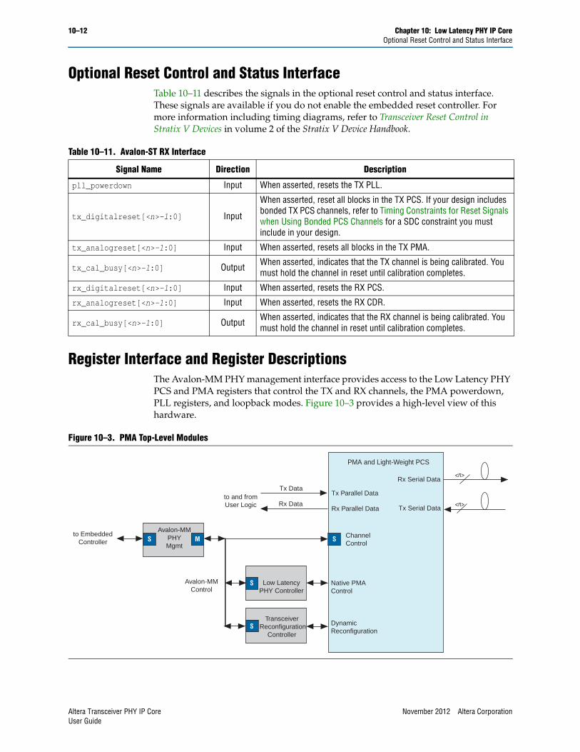
10–12 Chapter 10: Low Latency PHY IP CoreOptional Reset Control and Status Interface
Optional Reset Control and Status Interface Table 10–11 describes the signals in the optional reset control and status interface. These signals are available if you do not enable the embedded reset controller. For more information including timing diagrams, refer to Transceiver Reset Control in Stratix V Devices in volume 2 of the Stratix V Device Handbook.
Register Interface and Register DescriptionsThe Avalon-MM PHY management interface provides access to the Low Latency PHY PCS and PMA registers that control the TX and RX channels, the PMA powerdown, PLL registers, and loopback modes. Figure 10–3 provides a high-level view of this hardware.
Table 10–11. Avalon-ST RX Interface
Signal Name Direction Description
pll_powerdown Input When asserted, resets the TX PLL.
tx_digitalreset[<n>-1:0] Input
When asserted, reset all blocks in the TX PCS. If your design includes bonded TX PCS channels, refer to Timing Constraints for Reset Signals when Using Bonded PCS Channels for a SDC constraint you must include in your design.
tx_analogreset[<n>-1:0] Input When asserted, resets all blocks in the TX PMA.
tx_cal_busy[<n>-1:0] Output When asserted, indicates that the TX channel is being calibrated. You must hold the channel in reset until calibration completes.
rx_digitalreset[<n>-1:0] Input When asserted, resets the RX PCS.
rx_analogreset[<n>-1:0] Input When asserted, resets the RX CDR.
rx_cal_busy[<n>-1:0] Output When asserted, indicates that the RX channel is being calibrated. You must hold the channel in reset until calibration completes.
Figure 10–3. PMA Top-Level Modules
PMA and Light-Weight PCS
DynamicReconfiguration
Native PMAControl
ChannelControl
S
Avalon-MMControl
S
S
Low LatencyPHY Controller
Tx Data
to EmbeddedController
Transceiver Reconfiguration
Controller
to and fromUser Logic
Tx Parallel Data
Rx DataRx Parallel Data
MAvalon-MM
PHYMgmt
S
Rx Serial Data
Tx Serial Data<n>
<n>
Altera Transceiver PHY IP Core November 2012 Altera CorporationUser Guide
Chapter 10: Low Latency PHY IP Core 10–13Register Interface and Register Descriptions
Table 10–12 describes the signals in the PHY Management interface.
f For more information about the Avalon-MM and Avalon-ST protocols, including timing diagrams, refer to the Avalon Interface Specifications.
Table 10–13 describes the registers that you can access over the PHY Management Interface using word addresses and a 32-bit embedded processor.
1 Writing to reserved or undefined register addresses may have undefined side effects.
Table 10–12. Avalon-MM PHY Management Interface
Signal Name Direction Description
phy_mgmt_clk Input
Avalon-MM clock input. There is no frequency restriction for the phy_mgmt_clk; however, if you plan to use the same clock for the PHY management interface and transceiver reconfiguration, you must restrict the frequency range of phy_mgmt_clk to 100–150 MHz to meet the specification for the transceiver reconfiguration clock.
phy_mgmt_clk_reset Input Global reset signal. This signal is active high and level sensitive. This is an asynchronous signal.
phy_mgmtaddress[8:0] Input 9-bit Avalon-MM address.
phy_mgmt_writedata[31:0] Input Input data.
phy_mgmt_readdata[31:0] Output Output data.
phy_mgmt_write Input Write signal.
phy_mgmt_read Input Read signal.
Table 10–13. Low Latency PHY IP Core Registers (Part 1 of 2)
Word Addr Bits R/W Register Name Description
Reset Control Registers–Automatic Reset Controller
0x041 [31:0] RW reset_ch_bitmaskReset controller channel bitmask for digital resets. The default value is all 1s. Channel <n> can be reset when bit<n> = 1.
0x042 [1:0]
W reset_control (write)
Writing a 1 to bit 0 initiates a TX digital reset using the reset controller module. The reset affects channels enabled in the reset_ch_bitmask. Writing a 1 to bit 1 initiates a RX digital reset of channels enabled in the reset_ch_bitmask.
R reset_status(read)Reading bit 0 returns the status of the reset controller TX ready bit. Reading bit 1 returns the status of the reset controller RX ready bit.
November 2012 Altera Corporation Altera Transceiver PHY IP CoreUser Guide
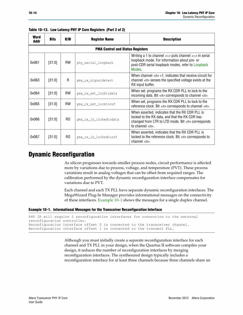
10–14 Chapter 10: Low Latency PHY IP CoreDynamic Reconfiguration
Dynamic ReconfigurationAs silicon progresses towards smaller process nodes, circuit performance is affected more by variations due to process, voltage, and temperature (PVT). These process variations result in analog voltages that can be offset from required ranges. The calibration performed by the dynamic reconfiguration interface compensates for variations due to PVT.
Each channel and each TX PLL have separate dynamic reconfiguration interfaces. The MegaWizard Plug-In Manager provides informational messages on the connectivity of these interfaces. Example 10–1 shows the messages for a single duplex channel.
Although you must initially create a separate reconfiguration interface for each channel and TX PLL in your design, when the Quartus II software compiles your design, it reduces the number of reconfiguration interfaces by merging reconfiguration interfaces. The synthesized design typically includes a reconfiguration interface for at least three channels because three channels share an
PMA Control and Status Registers
0x061 [31:0] RW phy_serial_loopback
Writing a 1 to channel <n> puts channel <n> in serial loopback mode. For information about pre- or post-CDR serial loopback modes, refer to Loopback Modes.
0x063 [31:0] R pma_rx_signaldetectWhen channel <n> =1, indicates that receive circuit for channel <n> senses the specified voltage exists at the RX input buffer.
0x064 [31:0] RW pma_rx_set_locktodataWhen set, programs the RX CDR PLL to lock to the incoming data. Bit <n> corresponds to channel <n>.
0x065 [31:0] RW pma_rx_set_locktorefWhen set, programs the RX CDR PLL to lock to the reference clock. Bit <n> corresponds to channel <n>.
0x066 [31:0] RO pma_rx_is_lockedtodata
When asserted, indicates that the RX CDR PLL is locked to the RX data, and that the RX CDR has changed from LTR to LTD mode. Bit <n> corresponds to channel <n>.
0x067 [31:0] RO pma_rx_is_lockedtorefWhen asserted, indicates that the RX CDR PLL is locked to the reference clock. Bit <n> corresponds to channel <n>.
Table 10–13. Low Latency PHY IP Core Registers (Part 2 of 2)
Word Addr Bits R/W Register Name Description
Example 10–1. Informational Messages for the Transceiver Reconfiguration Interface
PHY IP will require 2 reconfiguration interfaces for connection to the external reconfiguration controller.Reconfiguration interface offset 0 is connected to the transceiver channel.Reconfiguration interface offset 1 is connected to the transmit PLL.
Altera Transceiver PHY IP Core November 2012 Altera CorporationUser Guide
Chapter 10: Low Latency PHY IP Core 10–15Simulation Files and Example Testbench
Avalon-MM slave interface which connects to the Transceiver Reconfiguration Controller IP Core. Conversely, you cannot connect the three channels that share an Avalon-MM interface to different Transceiver Reconfiguration Controller IP Cores. Doing so causes a Fitter error. For more information, refer to Transceiver Reconfiguration Controller to PHY IP Connectivity.
Table 10–14 describes the signals in the reconfiguration interface. This interface uses a clock provided by the reconfiguration controller.
If you are using ×6 or ×N bonding, transceiver dynamic reconfiguration requires that you assign the starting channel number. Logical channel 0 should be assigned to either physical transceiver channel 1 or channel 4 of a transceiver bank. However, if you have already created a PCB with a different lane assignment for logical lane 0, you can use the workaound shown in Example 10–2 to remove this restriction. Example 10–2 redefines the pma_bonding_master parameter using the Quartus II Assignment Editor. In this example, the pma_bonding_master was originally assigned to physical channel 1. (The original assignment could also have been to physical channel 4.) The to parameter reassigns the pma_bonding_master to the Low Latency PHY instance name. You must substitute the instance name from your design for the instance name shown in quotation marks
Simulation Files and Example Testbench Refer to Running a Simulation Testbench for a description of the directories and files that the Quartus II software creates automatically when you generate your Low Latency PHY IP Core.
f Refer to the Altera wiki for an example testbench that you can use as a starting point in creating your own verification environment.
Table 10–14. Reconfiguration Interface
Signal Name Direction Description
reconfig_to_xcvr [(<n>70)-1:0] InputReconfiguration signals from the Transceiver Reconfiguration Controller. <n> grows linearly with the number of reconfiguration interfaces.
reconfig_from_xcvr [(<n>46)-1:0] OutputReconfiguration signals to the Transceiver Reconfiguration Controller. <n> grows linearly with the number of reconfiguration interfaces.
Example 10–2. Overriding Logical Channel 0 Channel Assignment Restrictions in Stratix V Devices for ×6 or ×N Bonding
set_parameter -name pma_bonding_master "\"1\"" -to "<low latency phy instance>|altera_xcvr_low_latency_phy:my_low_latency_phy_inst|sv_xcvr_low_latency_phy_nr:sv_xcvr_low_latency_phy_nr_inst|sv_xcvr_10g_custom_native:sv_xcvr_10g_custom_native_inst|sv_xcvr_native:sv_xcvr_native_insts[0].gen_bonded_group_native.sv_xcvr_native_inst"
November 2012 Altera Corporation Altera Transceiver PHY IP CoreUser Guide

10–16 Chapter 10: Low Latency PHY IP CoreSimulation Files and Example Testbench
Altera Transceiver PHY IP Core November 2012 Altera CorporationUser Guide
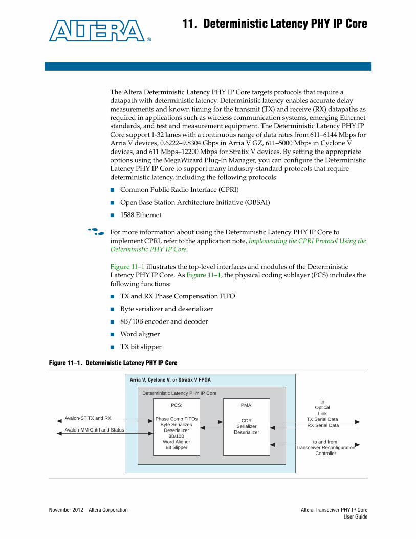
November 2012 Altera Corporation
11. Deterministic Latency PHY IP Core
The Altera Deterministic Latency PHY IP Core targets protocols that require a datapath with deterministic latency. Deterministic latency enables accurate delay measurements and known timing for the transmit (TX) and receive (RX) datapaths as required in applications such as wireless communication systems, emerging Ethernet standards, and test and measurement equipment. The Deterministic Latency PHY IP Core support 1-32 lanes with a continuous range of data rates from 611–6144 Mbps for Arria V devices, 0.6222–9.8304 Gbps in Arria V GZ, 611–5000 Mbps in Cyclone V devices, and 611 Mbps–12200 Mbps for Stratix V devices. By setting the appropriate options using the MegaWizard Plug-In Manager, you can configure the Deterministic Latency PHY IP Core to support many industry-standard protocols that require deterministic latency, including the following protocols:
■ Common Public Radio Interface (CPRI)
■ Open Base Station Architecture Initiative (OBSAI)
■ 1588 Ethernet
f For more information about using the Deterministic Latency PHY IP Core to implement CPRI, refer to the application note, Implementing the CPRI Protocol Using the Deterministic PHY IP Core.
Figure 11–1 illustrates the top-level interfaces and modules of the Deterministic Latency PHY IP Core. As Figure 11–1, the physical coding sublayer (PCS) includes the following functions:
■ TX and RX Phase Compensation FIFO
■ Byte serializer and deserializer
■ 8B/10B encoder and decoder
■ Word aligner
■ TX bit slipper
Figure 11–1. Deterministic Latency PHY IP Core
Deterministic Latency PHY IP Core
Arria V, Cyclone V, or Stratix V FPGA
PCS:
Phase Comp FIFOsByte Serializer/
Deserializer8B/10B
Word AlignerBit Slipper
PMA:
CDRSerializer
Deserializer
TX Serial DataRX Serial Data
toOptical
LinkAvalon-ST TX and RX
Avalon-MM Cntrl and Status
to and from Transceiver Reconfiguration
Controller
Altera Transceiver PHY IP CoreUser Guide
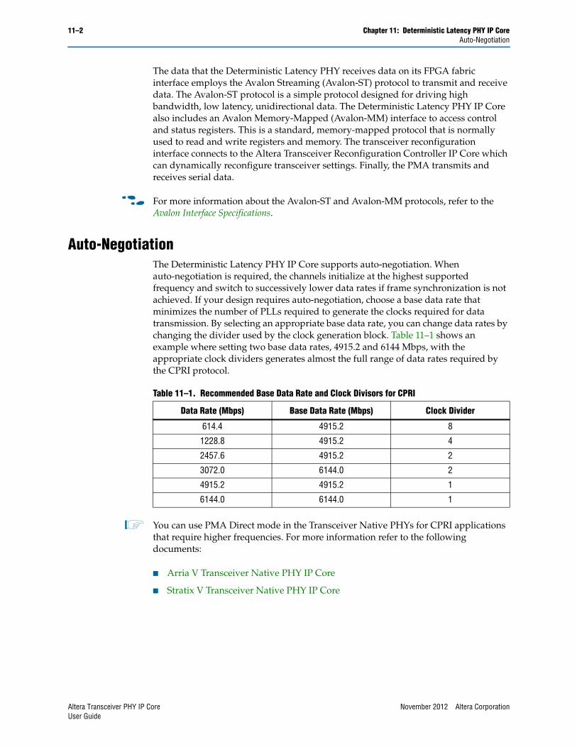
11–2 Chapter 11: Deterministic Latency PHY IP CoreAuto-Negotiation
The data that the Deterministic Latency PHY receives data on its FPGA fabric interface employs the Avalon Streaming (Avalon-ST) protocol to transmit and receive data. The Avalon-ST protocol is a simple protocol designed for driving high bandwidth, low latency, unidirectional data. The Deterministic Latency PHY IP Core also includes an Avalon Memory-Mapped (Avalon-MM) interface to access control and status registers. This is a standard, memory-mapped protocol that is normally used to read and write registers and memory. The transceiver reconfiguration interface connects to the Altera Transceiver Reconfiguration Controller IP Core which can dynamically reconfigure transceiver settings. Finally, the PMA transmits and receives serial data.
f For more information about the Avalon-ST and Avalon-MM protocols, refer to the Avalon Interface Specifications.
Auto-Negotiation The Deterministic Latency PHY IP Core supports auto-negotiation. When auto-negotiation is required, the channels initialize at the highest supported frequency and switch to successively lower data rates if frame synchronization is not achieved. If your design requires auto-negotiation, choose a base data rate that minimizes the number of PLLs required to generate the clocks required for data transmission. By selecting an appropriate base data rate, you can change data rates by changing the divider used by the clock generation block. Table 11–1 shows an example where setting two base data rates, 4915.2 and 6144 Mbps, with the appropriate clock dividers generates almost the full range of data rates required by the CPRI protocol.
1 You can use PMA Direct mode in the Transceiver Native PHYs for CPRI applications that require higher frequencies. For more information refer to the following documents:
■ Arria V Transceiver Native PHY IP Core
■ Stratix V Transceiver Native PHY IP Core
Table 11–1. Recommended Base Data Rate and Clock Divisors for CPRI
Data Rate (Mbps) Base Data Rate (Mbps) Clock Divider
614.4 4915.2 8
1228.8 4915.2 4
2457.6 4915.2 2
3072.0 6144.0 2
4915.2 4915.2 1
6144.0 6144.0 1
Altera Transceiver PHY IP Core November 2012 Altera CorporationUser Guide
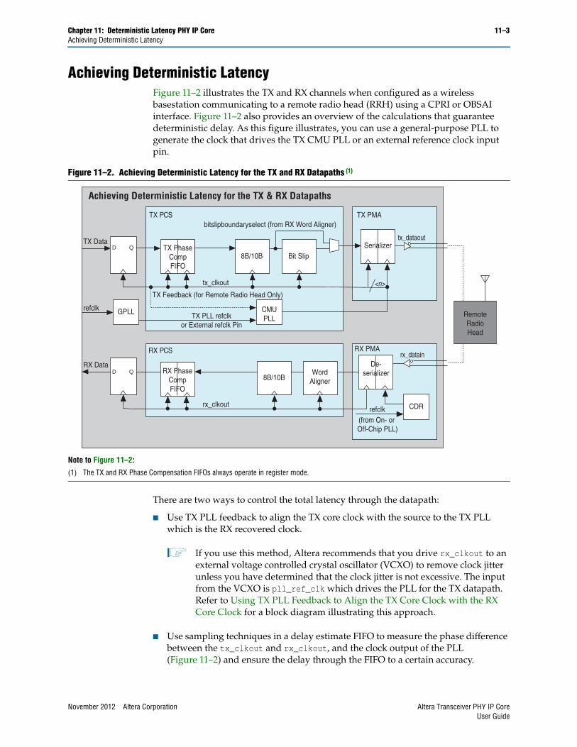
Chapter 11: Deterministic Latency PHY IP Core 11–3Achieving Deterministic Latency
Achieving Deterministic LatencyFigure 11–2 illustrates the TX and RX channels when configured as a wireless basestation communicating to a remote radio head (RRH) using a CPRI or OBSAI interface. Figure 11–2 also provides an overview of the calculations that guarantee deterministic delay. As this figure illustrates, you can use a general-purpose PLL to generate the clock that drives the TX CMU PLL or an external reference clock input pin.
There are two ways to control the total latency through the datapath:
■ Use TX PLL feedback to align the TX core clock with the source to the TX PLL which is the RX recovered clock.
1 If you use this method, Altera recommends that you drive rx_clkout to an external voltage controlled crystal oscillator (VCXO) to remove clock jitter unless you have determined that the clock jitter is not excessive. The input from the VCXO is pll_ref_clk which drives the PLL for the TX datapath. Refer to Using TX PLL Feedback to Align the TX Core Clock with the RX Core Clock for a block diagram illustrating this approach.
■ Use sampling techniques in a delay estimate FIFO to measure the phase difference between the tx_clkout and rx_clkout, and the clock output of the PLL (Figure 11–2) and ensure the delay through the FIFO to a certain accuracy.
Figure 11–2. Achieving Deterministic Latency for the TX and RX Datapaths (1)
Note to Figure 11–2:
(1) The TX and RX Phase Compensation FIFOs always operate in register mode.
TX Data
RX Data
bitslipboundaryselect (from RX Word Aligner)TX PMA
tx_dataoutD Q
D Q
Serializer
RX PMA
De-serializer
CMUPLL
GPLL
CDR
refclk
refclk (from On- or Off-Chip PLL)
<n>
8B/10B
rx_datainRX PCS
TX PCS
Achieving Deterministic Latency for the TX & RX Datapaths
RX PhaseCompFIFO
TX PhaseCompFIFO
tx_clkout
TX PLL refclkor External refclk Pin
TX Feedback (for Remote Radio Head Only)
rx_clkout
8B/10BWord
Aligner
Bit Slip
RemoteRadioHead
November 2012 Altera Corporation Altera Transceiver PHY IP CoreUser Guide
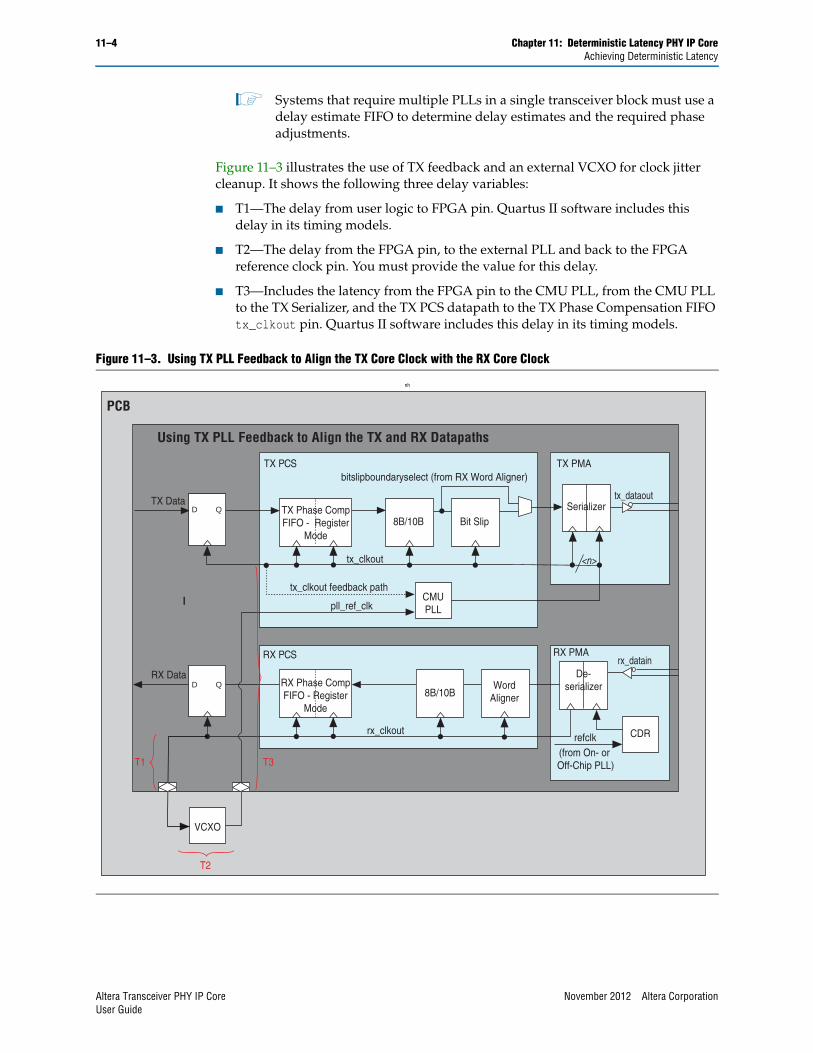
11–4 Chapter 11: Deterministic Latency PHY IP CoreAchieving Deterministic Latency
1 Systems that require multiple PLLs in a single transceiver block must use a delay estimate FIFO to determine delay estimates and the required phase adjustments.
Figure 11–3 illustrates the use of TX feedback and an external VCXO for clock jitter cleanup. It shows the following three delay variables:
■ T1—The delay from user logic to FPGA pin. Quartus II software includes this delay in its timing models.
■ T2—The delay from the FPGA pin, to the external PLL and back to the FPGA reference clock pin. You must provide the value for this delay.
■ T3—Includes the latency from the FPGA pin to the CMU PLL, from the CMU PLL to the TX Serializer, and the TX PCS datapath to the TX Phase Compensation FIFO tx_clkout pin. Quartus II software includes this delay in its timing models.
Figure 11–3. Using TX PLL Feedback to Align the TX Core Clock with the RX Core Clock
nh
TX Data
RX Data
T3
T2
T1
bitslipboundaryselect (from RX Word Aligner)TX PMA
tx_dataoutD Q
D Q
Serializer
RX PMA
De-serializer
CMUPLL
VCXO
CDRrefclk (from On- or Off-Chip PLL)
<n>
8B/10B
rx_datainRX PCS
TX PCS
Using TX PLL Feedback to Align the TX and RX Datapaths
PCB
tx_clkout
pll_ref_clk
tx_clkout feedback path
rx_clkout
8B/10BWord
Aligner
Bit Slip TX Phase Comp FIFO - Register
Mode
RX Phase CompFIFO - Register
Mode
Altera Transceiver PHY IP Core November 2012 Altera CorporationUser Guide
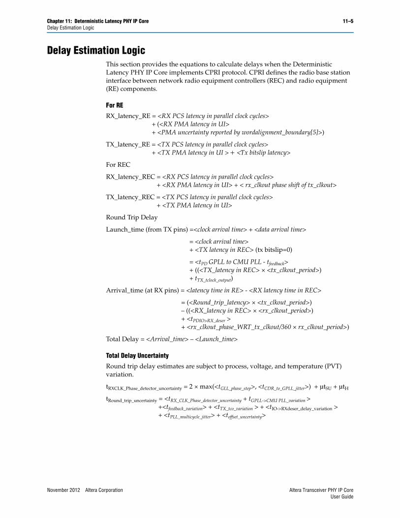
Chapter 11: Deterministic Latency PHY IP Core 11–5Delay Estimation Logic
Delay Estimation LogicThis section provides the equations to calculate delays when the Deterministic Latency PHY IP Core implements CPRI protocol. CPRI defines the radio base station interface between network radio equipment controllers (REC) and radio equipment (RE) components.
For RE
RX_latency_RE = <RX PCS latency in parallel clock cycles> + (<RX PMA latency in UI>
+ <PMA uncertainty reported by wordalignment_boundary[5]>)
TX_latency_RE = <TX PCS latency in parallel clock cycles>+ <TX PMA latency in UI > Tx bitslip latency>
For REC
RX_latency_REC = <RX PCS latency in parallel clock cycles>+ <RX PMA latency in UI> + < rx_clkout phase shift of tx_clkout>
TX_latency_REC = <TX PCS latency in parallel clock cycles>+ <TX PMA latency in UI>
Round Trip Delay
Launch_time (from TX pins) =<clock arrival time> + <data arrival time>
= <clock arrival time>+ <TX latency in REC> (tx bitslip=0)
= <tPD GPLL to CMU PLL - tfeedback>+ ((<TX_latency in REC> × <tx_clkout_period>)+ tTX_tclock_output)
Arrival_time (at RX pins) = <latency time in RE> - <RX latency time in REC>
= (<Round_trip_latency> × <tx_clkout_period>)– ((<RX_latency in REC> × <rx_clkout_period>) + <tPDIO>RX_deser >+ <rx_clkout_phase_WRT_tx_clkout/360 × rx_clkout_period>)
Total Delay = <Arrival_time> – <Launch_time>
Total Delay Uncertainty
Round trip delay estimates are subject to process, voltage, and temperature (PVT) variation.
tRXCLK_Phase_detector_uncertainty = 2 × max(<tGLL_phase_step>, <tCDR_to_GPLL_jitter>) + µtSU + µtH
tRound_trip_uncertainty = <tRX_CLK_Phase_detector_uncertainty + tGPLL->CMU PLL_variation >+<tfeedback_variation> + <tTX_tco_variation > + <tIO->RXdeser_delay_variation >+ <tPLL_multicycle_jitter> + <toffset_uncertainty>
November 2012 Altera Corporation Altera Transceiver PHY IP CoreUser Guide
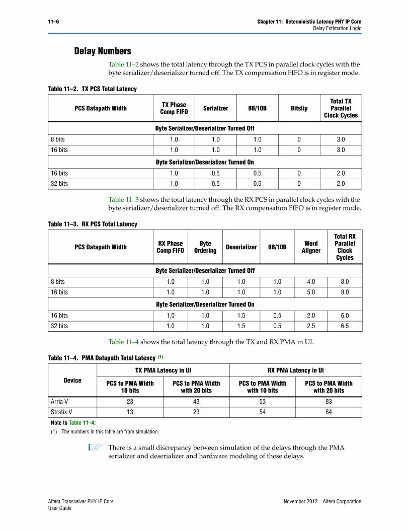
11–6 Chapter 11: Deterministic Latency PHY IP CoreDelay Estimation Logic
Delay NumbersTable 11–2 shows the total latency through the TX PCS in parallel clock cycles with the byte serializer/deserializer turned off. The TX compensation FIFO is in register mode.
Table 11–3 shows the total latency through the RX PCS in parallel clock cycles with the byte serializer/deserializer turned off. The RX compensation FIFO is in register mode.
Table 11–4 shows the total latency through the TX and RX PMA in UI.
1 There is a small discrepancy between simulation of the delays through the PMA serializer and deserializer and hardware modeling of these delays.
Table 11–2. TX PCS Total Latency
PCS Datapath Width TX Phase Comp FIFO Serializer 8B/10B Bitslip
Total TX Parallel
Clock Cycles
Byte Serializer/Deserializer Turned Off
8 bits 1.0 1.0 1.0 0 3.0
16 bits 1.0 1.0 1.0 0 3.0
Byte Serializer/Deserializer Turned On
16 bits 1.0 0.5 0.5 0 2.0
32 bits 1.0 0.5 0.5 0 2.0
Table 11–3. RX PCS Total Latency
PCS Datapath Width RX Phase Comp FIFO
Byte Ordering Deserializer 8B/10B Word
Aligner
Total RX Parallel Clock Cycles
Byte Serializer/Deserializer Turned Off
8 bits 1.0 1.0 1.0 1.0 4.0 8.0
16 bits 1.0 1.0 1.0 1.0 5.0 9.0
Byte Serializer/Deserializer Turned On
16 bits 1.0 1.0 1.5 0.5 2.0 6.0
32 bits 1.0 1.0 1.5 0.5 2.5 6.5
Table 11–4. PMA Datapath Total Latency (1)
Device
TX PMA Latency in UI RX PMA Latency in UI
PCS to PMA Width10 bits
PCS to PMA Width with 20 bits
PCS to PMA Width with 10 bits
PCS to PMA Width with 20 bits
Arria V 23 43 53 83
Stratix V 13 23 54 84
Note to Table 11–4:
(1) The numbers in this table are from simulation.
Altera Transceiver PHY IP Core November 2012 Altera CorporationUser Guide
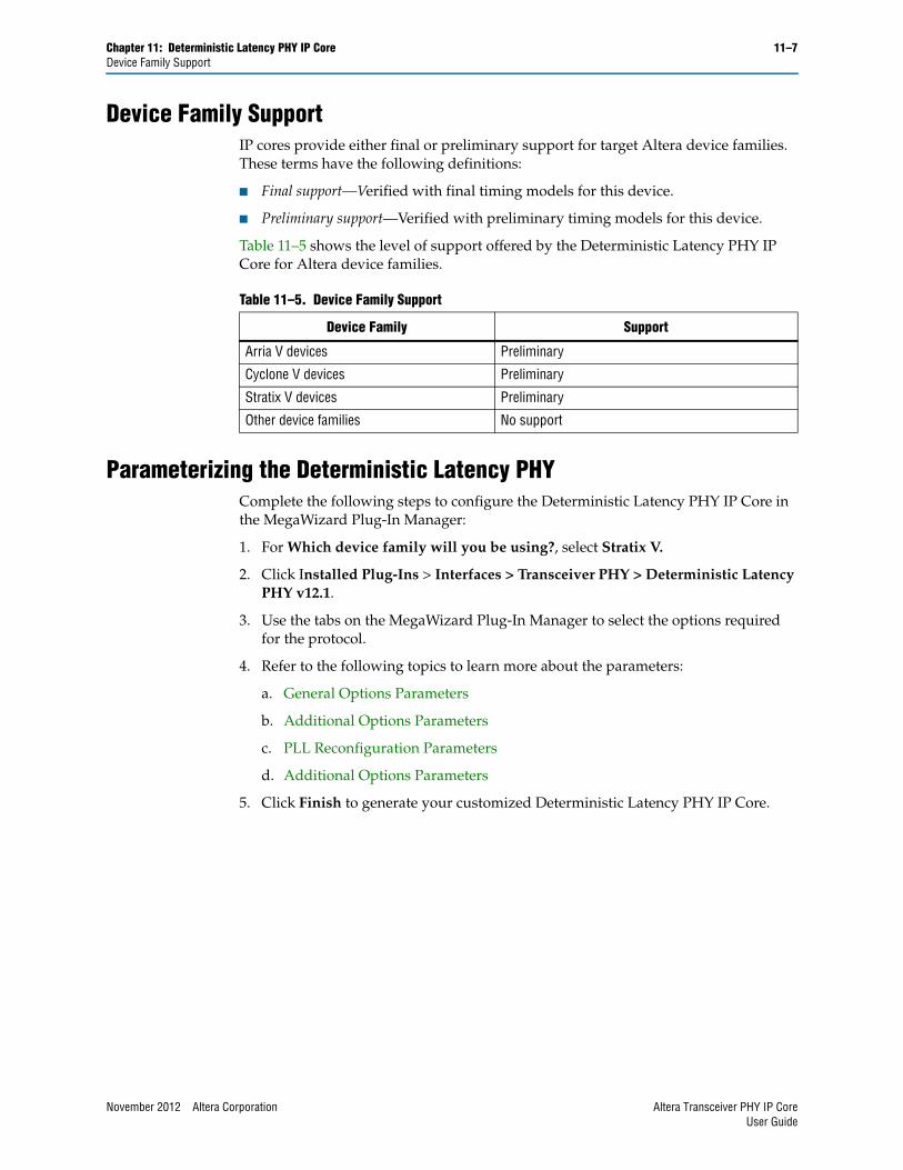
Chapter 11: Deterministic Latency PHY IP Core 11–7Device Family Support
Device Family SupportIP cores provide either final or preliminary support for target Altera device families. These terms have the following definitions:
■ Final support—Verified with final timing models for this device.
■ Preliminary support—Verified with preliminary timing models for this device.
Table 11–5 shows the level of support offered by the Deterministic Latency PHY IP Core for Altera device families.
Parameterizing the Deterministic Latency PHYComplete the following steps to configure the Deterministic Latency PHY IP Core in the MegaWizard Plug-In Manager:
1. For Which device family will you be using?, select Stratix V.
2. Click Installed Plug-Ins > Interfaces > Transceiver PHY > Deterministic Latency PHY v12.1.
3. Use the tabs on the MegaWizard Plug-In Manager to select the options required for the protocol.
4. Refer to the following topics to learn more about the parameters:
a. General Options Parameters
b. Additional Options Parameters
c. PLL Reconfiguration Parameters
d. Additional Options Parameters
5. Click Finish to generate your customized Deterministic Latency PHY IP Core.
Table 11–5. Device Family Support
Device Family Support
Arria V devices Preliminary
Cyclone V devices Preliminary
Stratix V devices Preliminary
Other device families No support
November 2012 Altera Corporation Altera Transceiver PHY IP CoreUser Guide
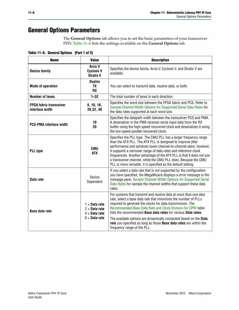
11–8 Chapter 11: Deterministic Latency PHY IP CoreGeneral Options Parameters
General Options ParametersThe General Options tab allows you to set the basic parameters of your transceiver PHY. Table 11–6 lists the settings available on the General Options tab.
Table 11–6. General Options (Part 1 of 2)
Name Value Description
Device familyArria V
Cyclone VStratix V
Specifies the device family. Arria V, Cyclone V, and Stratix V are available.
Mode of operationDuplex
TXRX
You can select to transmit data, receive data, or both.
Number of lanes 1–32 The total number of lanes in each direction.
FPGA fabric transceiver interface width
8, 10, 16, 20,32, 40
Specifies the word size between the FPGA fabric and PCS. Refer to Sample Channel WIdth Options for Supported Serial Data Rates for the data rates supported at each word size.
PCS-PMA interface width 1020
Specifies the datapath width between the transceiver PCS and PMA. A deserializer in the PMA receives serial input data from the RX buffer using the high-speed recovered clock and deserializes it using the low-speed parallel recovered clock.
PLL type CMUATX
Specifies the PLL type. The CMU PLL has a larger frequency range than the ATX PLL. The ATX PLL is designed to improve jitter performance and achieves lower channel-to-channel skew; however, it supports a narrower range of data rates and reference clock frequencies. Another advantage of the ATX PLL is that it does not use a transceiver channel, while the CMU PLL does. Because the CMU PLL is more versatile, it is specified as the default setting.
Data rate Device Dependent
If you select a data rate that is not supported by the configuration you have specified, the MegaWizard displays a error message in the message pane. Sample Channel WIdth Options for Supported Serial Data Rates for sample the channel widths that support these data rates.
Base data rate
1 × Data rate2 × Data rate4 × Data rate8 × Data rate
For systems that transmit and receive data at more than one data rate, select a base data rate that minimizes the number of PLLs required to generate the clocks for data transmission. The Recommended Base Data Rate and Clock Divisors for CPRI table lists the recommended Base data rates for various Data rates.
The available options are dynamically computed based on the Data rate you specified as long as those Base data rates are within the frequency range of the PLL.
Altera Transceiver PHY IP Core November 2012 Altera CorporationUser Guide
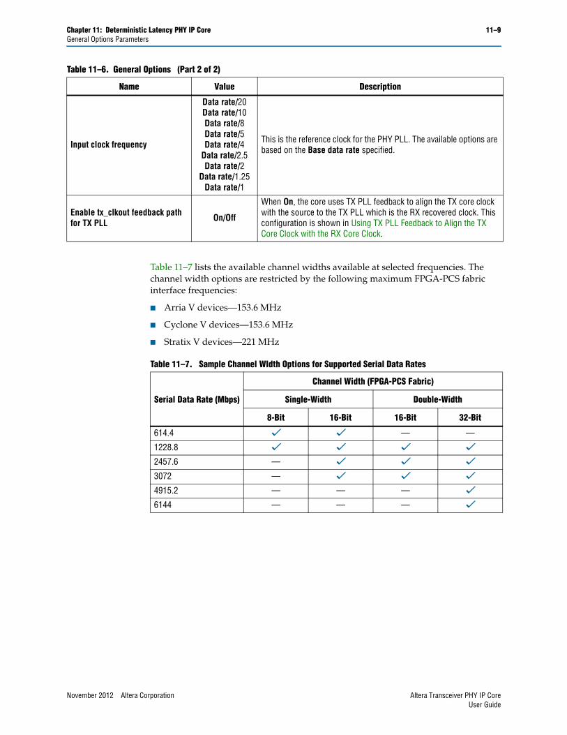
Chapter 11: Deterministic Latency PHY IP Core 11–9General Options Parameters
Table 11–7 lists the available channel widths available at selected frequencies. The channel width options are restricted by the following maximum FPGA-PCS fabric interface frequencies:
■ Arria V devices—153.6 MHz
■ Cyclone V devices—153.6 MHz
■ Stratix V devices—221 MHz
Input clock frequency
Data rate/20 Data rate/10 Data rate/8Data rate/5Data rate/4
Data rate/2.5Data rate/2
Data rate/1.25Data rate/1
This is the reference clock for the PHY PLL. The available options are based on the Base data rate specified.
Enable tx_clkout feedback path for TX PLL On/Off
When On, the core uses TX PLL feedback to align the TX core clock with the source to the TX PLL which is the RX recovered clock. This configuration is shown in Using TX PLL Feedback to Align the TX Core Clock with the RX Core Clock.
Table 11–6. General Options (Part 2 of 2)
Name Value Description
Table 11–7. Sample Channel WIdth Options for Supported Serial Data Rates
Serial Data Rate (Mbps)
Channel Width (FPGA-PCS Fabric)
Single-Width Double-Width
8-Bit 16-Bit 16-Bit 32-Bit
614.4 v v — —
1228.8 v v v v2457.6 — v v v3072 — v v v4915.2 — — — v6144 — — — v
November 2012 Altera Corporation Altera Transceiver PHY IP CoreUser Guide
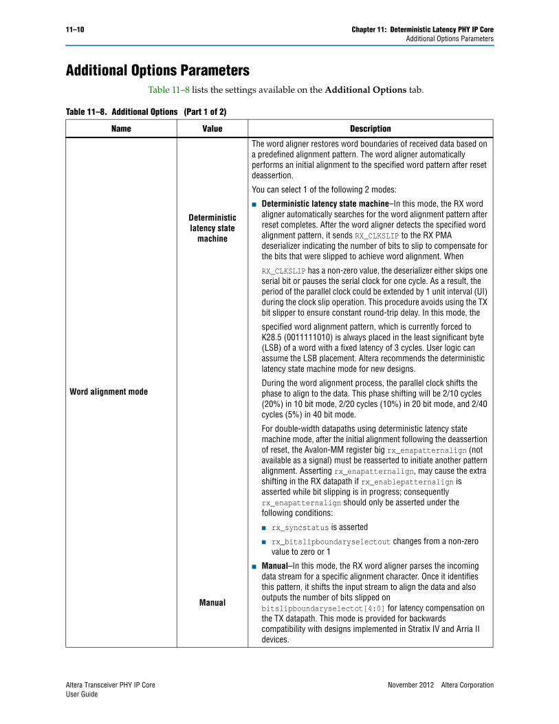
11–10 Chapter 11: Deterministic Latency PHY IP CoreAdditional Options Parameters
Additional Options ParametersTable 11–8 lists the settings available on the Additional Options tab.
Table 11–8. Additional Options (Part 1 of 2)
Name Value Description
Word alignment mode
Deterministic latency state
machine
The word aligner restores word boundaries of received data based on a predefined alignment pattern. The word aligner automatically performs an initial alignment to the specified word pattern after reset deassertion.
You can select 1 of the following 2 modes:
■ Deterministic latency state machine–In this mode, the RX word aligner automatically searches for the word alignment pattern after reset completes. After the word aligner detects the specified word alignment pattern, it sends RX_CLKSLIP to the RX PMA deserializer indicating the number of bits to slip to compensate for the bits that were slipped to achieve word alignment. When
RX_CLKSLIP has a non-zero value, the deserializer either skips one serial bit or pauses the serial clock for one cycle. As a result, the period of the parallel clock could be extended by 1 unit interval (UI) during the clock slip operation. This procedure avoids using the TX bit slipper to ensure constant round-trip delay. In this mode, the
specified word alignment pattern, which is currently forced to K28.5 (0011111010) is always placed in the least significant byte (LSB) of a word with a fixed latency of 3 cycles. User logic can assume the LSB placement. Altera recommends the deterministic latency state machine mode for new designs.
During the word alignment process, the parallel clock shifts the phase to align to the data. This phase shifting will be 2/10 cycles (20%) in 10 bit mode, 2/20 cycles (10%) in 20 bit mode, and 2/40 cycles (5%) in 40 bit mode.
For double-width datapaths using deterministic latency state machine mode, after the initial alignment following the deassertion of reset, the Avalon-MM register big rx_enapatternalign (not available as a signal) must be reasserted to initiate another pattern alignment. Asserting rx_enapatternalign, may cause the extra shifting in the RX datapath if rx_enablepatternalign is asserted while bit slipping is in progress; consequently rx_enapatternalign should only be asserted under the following conditions:
■ rx_syncstatus is asserted
■ rx_bitslipboundaryselectout changes from a non-zero value to zero or 1
Manual
■ Manual–In this mode, the RX word aligner parses the incoming data stream for a specific alignment character. Once it identifies this pattern, it shifts the input stream to align the data and also outputs the number of bits slipped on bitslipboundaryselectot[4:0] for latency compensation on the TX datapath. This mode is provided for backwards compatibility with designs implemented in Stratix IV and Arria II devices.
Altera Transceiver PHY IP Core November 2012 Altera CorporationUser Guide
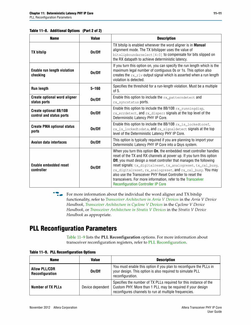
Chapter 11: Deterministic Latency PHY IP Core 11–11PLL Reconfiguration Parameters
f For more information about the individual the word aligner and TX bitslip functionality, refer to Transceiver Architecture in Arria V Devices in the Arria V Device Handbook, Transceiver Architecture in Cyclone V Devices in the Cyclone V Device Handbook, or Transceiver Architecture in Stratix V Devices in the Stratix V Device Handbook as appropriate.
PLL Reconfiguration ParametersTable 11–9 lists the PLL Reconfiguration options. For more information about transceiver reconfiguration registers, refer to PLL Reconfiguration.
TX bitslip On/Off
TX bitslip is enabled whenever the word aligner is in Manual alignment mode. The TX bitslipper uses the value of bitslipboundarselect[4:0] to compensate for bits slipped on the RX datapath to achieve deterministic latency.
Enable run length violation checking On/Off
If you turn this option on, you can specify the run length which is the maximum legal number of contiguous 0s or 1s. This option also creates the rx_rlv output signal which is asserted when a run length violation is detected.
Run length 5–160 Specifies the threshold for a run-length violation. Must be a multiple of 5.
Create optional word aligner status ports On/Off Enable this option to include the rx_patterndetect and
rx_syncstatus ports.
Create optional 8B/10B control and status ports On/Off
Enable this option to include the 8B/10B rx_runningdisp, rx_errdetect, and rx_disperr signals at the top level of the Deterministic Latency PHY IP Core.
Create PMA optional status ports On/Off
Enable this option to include the 8B/10B rx_is_lockedtoref, rx_is_lockedtodata, and rx_signaldetect signals at the top level of the Deterministic Latency PHY IP Core.
Avalon data interfaces On/Off This option is typically required if you are planning to import your Deterministic Latency PHY IP Core into a Qsys system.
Enable embedded reset controller On/Off
When you turn this option On, the embedded reset controller handles reset of the TX and RX channels at power up. If you turn this option Off, you must design a reset controller that manages the following reset signals: tx_digitalreset, tx_analogreset, tx_cal_busy, rx_digitalreset, rx_analogreset, and rx_cal_busy. You may also use the Transceiver PHY Reset Controller to reset the transceivers. For more information, refer to the Transceiver Reconfiguration Controller IP Core
Table 11–8. Additional Options (Part 2 of 2)
Name Value Description
Table 11–9. PLL Reconfiguration Options
Name Value Description
Allow PLL/CDR Reconfiguration On/Off
You must enable this option if you plan to reconfigure the PLLs in your design. This option is also required to simulate PLL reconfiguration.
Number of TX PLLs Device dependentSpecifies the number of TX PLLs required for this instance of the Custom PHY. More than 1 PLL may be required if your design reconfigures channels to run at multiple frequencies.
November 2012 Altera Corporation Altera Transceiver PHY IP CoreUser Guide
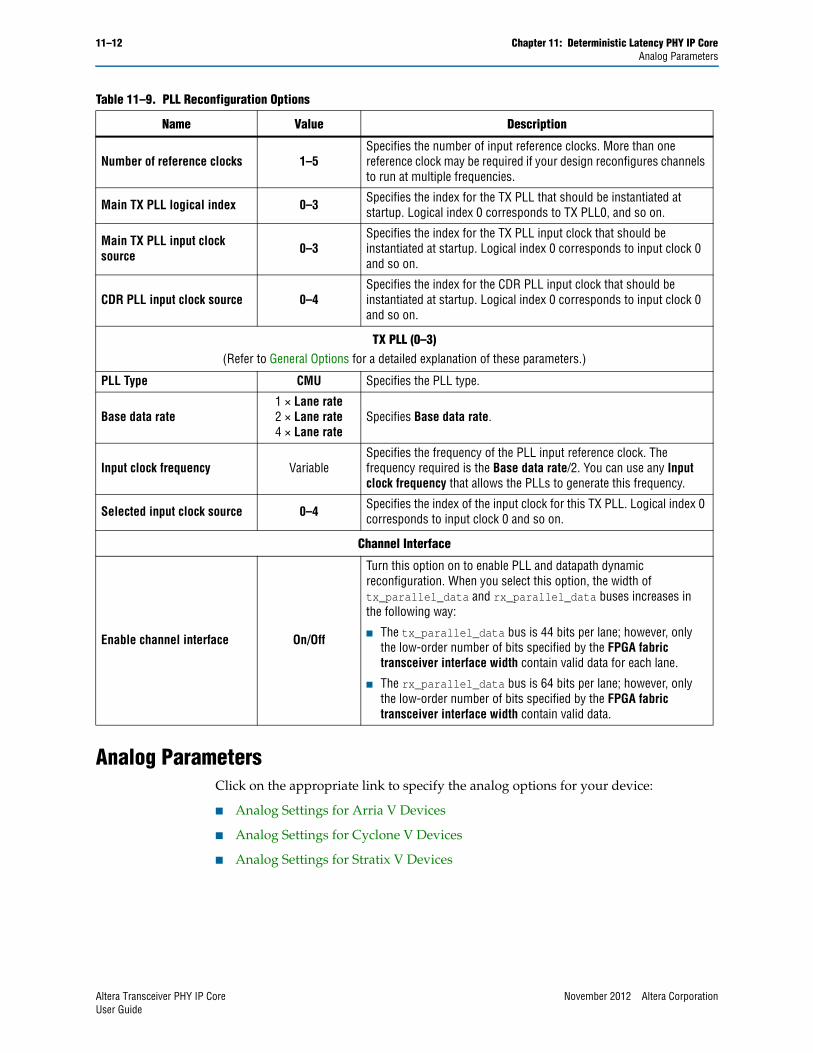
11–12 Chapter 11: Deterministic Latency PHY IP CoreAnalog Parameters
Analog Parameters Click on the appropriate link to specify the analog options for your device:
■ Analog Settings for Arria V Devices
■ Analog Settings for Cyclone V Devices
■ Analog Settings for Stratix V Devices
Number of reference clocks 1–5Specifies the number of input reference clocks. More than one reference clock may be required if your design reconfigures channels to run at multiple frequencies.
Main TX PLL logical index 0–3 Specifies the index for the TX PLL that should be instantiated at startup. Logical index 0 corresponds to TX PLL0, and so on.
Main TX PLL input clock source 0–3
Specifies the index for the TX PLL input clock that should be instantiated at startup. Logical index 0 corresponds to input clock 0 and so on.
CDR PLL input clock source 0–4Specifies the index for the CDR PLL input clock that should be instantiated at startup. Logical index 0 corresponds to input clock 0 and so on.
TX PLL (0–3)(Refer to General Options for a detailed explanation of these parameters.)
PLL Type CMU Specifies the PLL type.
Base data rate1 × Lane rate2 × Lane rate4 × Lane rate
Specifies Base data rate.
Input clock frequency VariableSpecifies the frequency of the PLL input reference clock. The frequency required is the Base data rate/2. You can use any Input clock frequency that allows the PLLs to generate this frequency.
Selected input clock source 0–4 Specifies the index of the input clock for this TX PLL. Logical index 0 corresponds to input clock 0 and so on.
Channel Interface
Enable channel interface On/Off
Turn this option on to enable PLL and datapath dynamic reconfiguration. When you select this option, the width of tx_parallel_data and rx_parallel_data buses increases in the following way:
■ The tx_parallel_data bus is 44 bits per lane; however, only the low-order number of bits specified by the FPGA fabric transceiver interface width contain valid data for each lane.
■ The rx_parallel_data bus is 64 bits per lane; however, only the low-order number of bits specified by the FPGA fabric transceiver interface width contain valid data.
Table 11–9. PLL Reconfiguration Options
Name Value Description
Altera Transceiver PHY IP Core November 2012 Altera CorporationUser Guide
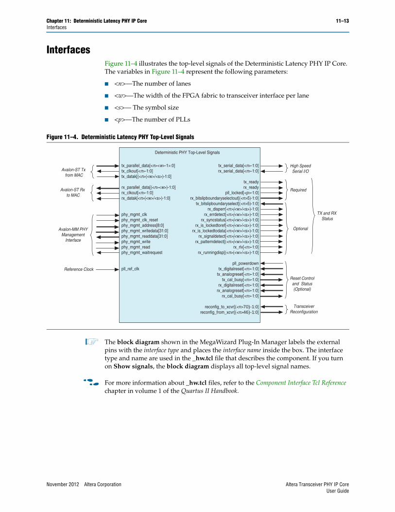
Chapter 11: Deterministic Latency PHY IP Core 11–13Interfaces
InterfacesFigure 11–4 illustrates the top-level signals of the Deterministic Latency PHY IP Core. The variables in Figure 11–4 represent the following parameters:
■ <n>—The number of lanes
■ <w>—The width of the FPGA fabric to transceiver interface per lane
■ <s>— The symbol size
■ <p>—The number of PLLs
1 The block diagram shown in the MegaWizard Plug-In Manager labels the external pins with the interface type and places the interface name inside the box. The interface type and name are used in the _hw.tcl file that describes the component. If you turn on Show signals, the block diagram displays all top-level signal names.
f For more information about _hw.tcl files, refer to the Component Interface Tcl Reference chapter in volume 1 of the Quartus II Handbook.
Figure 11–4. Deterministic Latency PHY Top-Level Signals
tx_parallel_data[<n><w>-1>:0]tx_clkout[<n>-1:0]tx_datak[(<n>(<w>/<s>)-1:0]
rx_parallel_data[(<n><w>)-1:0]rx_clkout[<n>-1:0]rx_datak[<n>(<w>/<s>)-1:0]
phy_mgmt_clkphy_mgmt_clk_resetphy_mgmt_address[8:0]phy_mgmt_writedata[31:0]phy_mgmt_readdata[31:0]phy_mgmt_writephy_mgmt_readphy_mgmt_waitrequest
pll_ref_clk
Deterministic PHY Top-Level Signals
tx_serial_data[<n>-1:0]rx_serial_data[<n>-1:0]
tx_readyrx_ready
pll_locked[<p>-1:0]rx_bitslipboundaryselectout[(<n>5)-1:0]
tx_bitslipboundaryselect[(<n>5)-1:0]rx_disperr[<n>(<w>/<s>)-1:0]
rx_errdetect[<n>(<w>/<s>)-1:0]rx_syncstatus[<n>(<w>/<s>)-1:0]
rx_is_lockedtoref[<n>(<w>/<s>)-1:0]rx_is_lockedtodata[<n>(<w>/<s>)-1:0]
rx_signaldetect[<n>(<w>/<s>)-1:0]rx_patterndetect[(<n>(<w>/<s>)-1:0]
rx_rlv[<n>-1:0]rx_runningdisp[(<n>(<w>/<s>)-1:0]
pll_powerdowntx_digitalreset[<n>-1:0]
tx_analogreset[<n>-1:0]tx_cal_busy[<n>-1:0]
rx_digitalreset[<n>-1:0]rx_analogreset[<n>-1:0]
rx_cal_busy[<n>-1:0]
reconfig_to_xcvr[(<n>70)-1:0]reconfig_from_xcvr[(<n>46)-1:0]
Avalon-ST Tx from MAC
High SpeedSerial I/O
Avalon-MM PHYManagement
Interface
Reference Clock
Reset Controland Status(Optional)
Optional
Required
TX and RX Status
Avalon-ST Rx to MAC
TransceiverReconfiguration
November 2012 Altera Corporation Altera Transceiver PHY IP CoreUser Guide
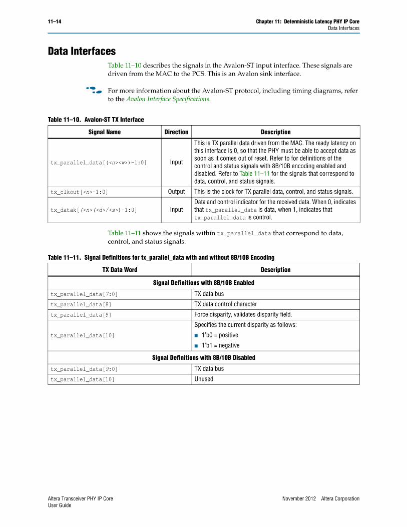
11–14 Chapter 11: Deterministic Latency PHY IP CoreData Interfaces
Data InterfacesTable 11–10 describes the signals in the Avalon-ST input interface. These signals are driven from the MAC to the PCS. This is an Avalon sink interface.
f For more information about the Avalon-ST protocol, including timing diagrams, refer to the Avalon Interface Specifications.
Table 11–11 shows the signals within tx_parallel_data that correspond to data, control, and status signals.
Table 11–10. Avalon-ST TX Interface
Signal Name Direction Description
tx_parallel_data[(<n><w>)-1:0] Input
This is TX parallel data driven from the MAC. The ready latency on this interface is 0, so that the PHY must be able to accept data as soon as it comes out of reset. Refer to for definitions of the control and status signals with 8B/10B encoding enabled and disabled. Refer to Table 11–11 for the signals that correspond to data, control, and status signals.
tx_clkout[<n>-1:0] Output This is the clock for TX parallel data, control, and status signals.
tx_datak[(<n>(<d>/<s>)-1:0] InputData and control indicator for the received data. When 0, indicates that tx_parallel_data is data, when 1, indicates that tx_parallel_data is control.
Table 11–11. Signal Definitions for tx_parallel_data with and without 8B/10B Encoding
TX Data Word Description
Signal Definitions with 8B/10B Enabled
tx_parallel_data[7:0] TX data bus
tx_parallel_data[8] TX data control character
tx_parallel_data[9] Force disparity, validates disparity field.
tx_parallel_data[10]
Specifies the current disparity as follows:
■ 1’b0 = positive
■ 1’b1 = negative
Signal Definitions with 8B/10B Disabled
tx_parallel_data[9:0] TX data bus
tx_parallel_data[10] Unused
Altera Transceiver PHY IP Core November 2012 Altera CorporationUser Guide
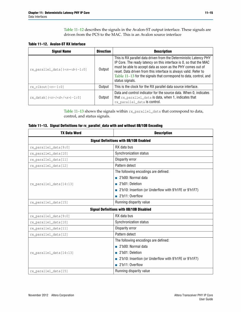
Chapter 11: Deterministic Latency PHY IP Core 11–15Data Interfaces
Table 11–12 describes the signals in the Avalon-ST output interface. These signals are driven from the PCS to the MAC. This is an Avalon source interface
Table 11–13 shows the signals within rx_parallel_data that correspond to data, control, and status signals.
Table 11–12. Avalon-ST RX Interface
Signal Name Direction Description
rx_parallel_data[(<n><d>)-1:0] Output
This is RX parallel data driven from the Deterministic Latency PHY IP Core. The ready latency on this interface is 0, so that the MAC must be able to accept data as soon as the PHY comes out of reset. Data driven from this interface is always valid. Refer to Table 11–13 for the signals that correspond to data, control, and status signals.
rx_clkout[<n>-1:0] Output This is the clock for the RX parallel data source interface.
rx_datak[(<n>(<d>/<s>)-1:0] OutputData and control indicator for the source data. When 0, indicates that rx_parallel_data is data, when 1, indicates that rx_parallel_data is control.
Table 11–13. Signal Definitions for rx_parallel_data with and without 8B/10B Encoding
TX Data Word Description
Signal Definitions with 8B/10B Enabled
rx_parallel_data[9:0] RX data bus
rx_parallel_data[10] Synchronization status
rx_parallel_data[11] Disparity error
rx_parallel_data[12] Pattern detect
rx_parallel_data[14:13]
The following encodings are defined:
■ 2’b00: Normal data
■ 2’b01: Deletion
■ 2’b10: Insertion (or Underflow with 9’h1FE or 9’h1F7)
■ 2’b11: Overflow
rx_parallel_data[15] Running disparity value
Signal Definitions with 8B/10B Disabled
rx_parallel_data[9:0] RX data bus
rx_parallel_data[10] Synchronization status
rx_parallel_data[11] Disparity error
rx_parallel_data[12] Pattern detect
rx_parallel_data[14:13]
The following encodings are defined:
■ 2’b00: Normal data
■ 2’b01: Deletion
■ 2’b10: Insertion (or Underflow with 9’h1FE or 9’h1F7)
■ 2’b11: Overflow
rx_parallel_data[15] Running disparity value
November 2012 Altera Corporation Altera Transceiver PHY IP CoreUser Guide
11–16 Chapter 11: Deterministic Latency PHY IP CoreClock Interface
Table 11–14 describes the differential serial data interface and the status signals for the transceiver serial data interface.
Clock InterfaceTable 11–15 describes clocks for the Deterministic Latency PHY. The input reference clock, pll_ref_clk, drives a PLL inside the PHY-layer block, and a PLL output clock, rx_clkout is used for all data, command, and status inputs and outputs.
Optional TX and RX Status InterfaceTable 11–16 describes the optional status signals for the RX interface.
Table 11–14. Serial Interface and Status Signals (1)
Signal Name Direction Signal Name
rx_serial_data[<n>-1:0] Input Receiver differential serial input data.
tx_serial_data[<n>-1:0] Output Transmitter differential serial output data.
Note to Table 11–14:
(1) <n> is the number of lanes.
Table 11–15. Clock Signals
Signal Name Direction Description
pll_ref_clk Input Reference clock for the PHY PLLs. Frequency range is 60–700 MHz.
Table 11–16. Serial Interface and Status Signals (Part 1 of 2) (1)
Signal Name Direction Signal Name
tx_ready Output When asserted, indicates that the TX interface has exited the reset state and is ready to transmit.
rx_ready Output When asserted, indicates that the RX interface has exited the reset state and is ready to receive.
pll_locked[<p>-1:0] Output When asserted, indicates that the PLL is locked to the input reference clock.
rx_bitslipboundaryselectout
[(<n>5)-1:0]Output
Specifies the number of bits slipped to achieve word alignment. In 3G (10-bit) mode, the output is the number of bits slipped. If no bits were slipped, the output is 0. In 6G (20-bit) mode, the output is (19 the number of bits slipped). If no bits were slipped, the output is 19. The default value of rx_bitslipboundaryselectout[4:0] before alignment is achieved is 5'b01111 in 3G mode and 5'b11111 in 6G mode.
Optional Status Signals
tx_bitslipboundaryselect[(<n>5)-1:0]
InputThis signal is used for bit slip word alignment mode. It selects the number of bits that the TX block must slip to achieve a deterministic latency.
rx_disperr[(<n>(<d>/<s>)-1:0] Output When asserted, indicates that the received 10-bit code or data group has a disparity error.
Altera Transceiver PHY IP Core November 2012 Altera CorporationUser Guide
Chapter 11: Deterministic Latency PHY IP Core 11–17Optional Reset Control and Status Interfaces
Optional Reset Control and Status InterfacesTable 11–17 describes the signals in the optional reset control and status interface. These signals are available if you do not enable the embedded reset controller.
f For more information about manual control of the reset sequence refer to Transceiver Reset Control in Arria V Devices, Transceiver Reset Control in Cyclone V Devices or Transceiver Reset Control in Stratix V Devices as appropriate.
rx_errdetect[(<n>(<d>/<s>)-1:0] Output When asserted, indicates that a received 10-bit code group has an 8B/10B code violation or disparity error.
rx_syncstatus[(<n>(<d>/<s>)-1:0] Output
Indicates presence or absence of synchronization on the RX interface. Asserted when word aligner identifies the word alignment pattern or synchronization code groups in the received data stream. This signal is optional.
rx_is_lockedtoref[(<n>(<d>/<s>)-1:0] OutputAsserted when the receiver CDR is locked to the input reference clock. This signal is asynchronous. This signal is optional.
rx_is_lockedtodata[(<n>(<d>/<s>)-1:0] Output
When asserted, the receiver CDR is in to lock-to-data mode. When deasserted, the receiver CDR lock mode depends on the rx_locktorefclk signal level. This signal is optional.
rx_patterndetect[(<n>(<d>/<s>)-1:0] OutputWhen asserted, indicates that the programmed word alignment pattern has been detected in the current word boundary.
rx_rlv[<n>-1:0] OutputWhen asserted, indicates a run length violation. Asserted if the number of consecutive 1s or 0s exceeds the number specified using the MegaWizard Plug-In Manager.
rx_runningdisp[(<n>(<d>/<s>)-1:0] Output This status signal indicates the disparity of the incoming data.
Table 11–16. Serial Interface and Status Signals (Part 2 of 2) (1)
Signal Name Direction Signal Name
Table 11–17. Avalon-ST RX Interface
Signal Name Direction Description
pll_powerdown[<n>-1:0] Input When asserted, resets the TX PLL.
tx_digitalreset[<n>-1:0] Input When asserted, reset all blocks in the TX PCS.
tx_analogreset[<n>-1:0] Input When asserted, resets all blocks in the TX PMA.
tx_cal_busy[<n>-1:0] Output When asserted, indicates that the TX channel is being calibrated. You must hold the channel in reset until calibration completes.
rx_digitalreset[<n>-1:0] Input When asserted, resets the RX PCS.
rx_analogreset[<n>-1:0] Input When asserted, resets the RX CDR.
rx_cal_busy[<n>-1:0] Output When asserted, indicates that the RX channel is being calibrated. You must hold the channel in reset until calibration completes.
November 2012 Altera Corporation Altera Transceiver PHY IP CoreUser Guide
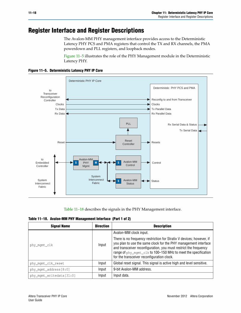
11–18 Chapter 11: Deterministic Latency PHY IP CoreRegister Interface and Register Descriptions
Register Interface and Register DescriptionsThe Avalon-MM PHY management interface provides access to the Deterministic Latency PHY PCS and PMA registers that control the TX and RX channels, the PMA powerdown and PLL registers, and loopback modes.
Figure 11–5 illustrates the role of the PHY Management module in the Deterministic Latency PHY.
Table 11–18 describes the signals in the PHY Management interface.
Figure 11–5. Deterministic Latency PHY IP Core
System Interconnect
FabricSystem
InterconnectFabric
Deterministic PHY PCS and PMA
Deterministic PHY IP Core
Resets
Status
ControlS Avalon-MMControl
S Avalon-MMStatus
ResetController
PLL
Reset
Clocks Clocks
toTransceiver
ReconfigurationController
toEmbeddedController
Tx Data Tx Parallel Data
Rx Data Rx Parallel Data
MAvalon-MM
PHYMgmt
S
Rx Serial Data & Status
Reconfig to and from Transceiver
Tx Serial Data
Table 11–18. Avalon-MM PHY Management Interface (Part 1 of 2)
Signal Name Direction Description
phy_mgmt_clk Input
Avalon-MM clock input.
There is no frequency restriction for Stratix V devices; however, if you plan to use the same clock for the PHY management interface and transceiver reconfiguration, you must restrict the frequency range of phy_mgmt_clk to 100–150 MHz to meet the specification for the transceiver reconfiguration clock.
phy_mgmt_clk_reset Input Global reset signal. This signal is active high and level sensitive.
phy_mgmt_address[8:0] Input 9-bit Avalon-MM address.
phy_mgmt_writedata[31:0] Input Input data.
Altera Transceiver PHY IP Core November 2012 Altera CorporationUser Guide
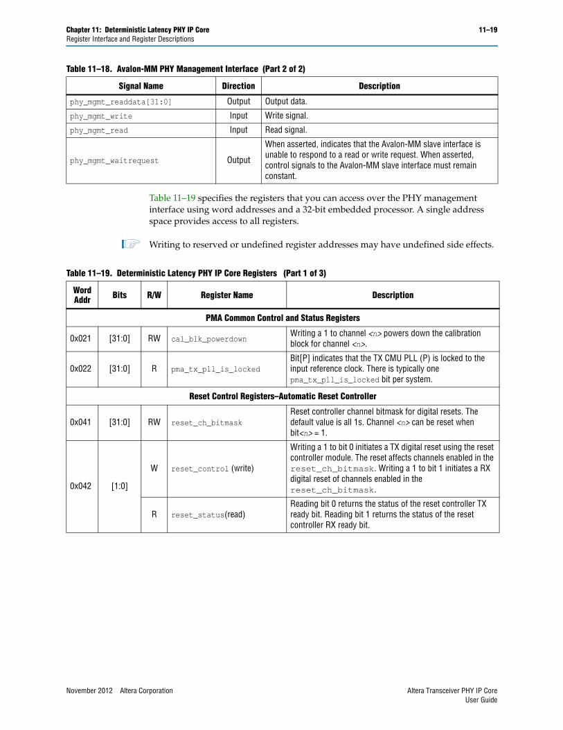
Chapter 11: Deterministic Latency PHY IP Core 11–19Register Interface and Register Descriptions
Table 11–19 specifies the registers that you can access over the PHY management interface using word addresses and a 32-bit embedded processor. A single address space provides access to all registers.
1 Writing to reserved or undefined register addresses may have undefined side effects.
phy_mgmt_readdata[31:0] Output Output data.
phy_mgmt_write Input Write signal.
phy_mgmt_read Input Read signal.
phy_mgmt_waitrequest Output
When asserted, indicates that the Avalon-MM slave interface is unable to respond to a read or write request. When asserted, control signals to the Avalon-MM slave interface must remain constant.
Table 11–18. Avalon-MM PHY Management Interface (Part 2 of 2)
Signal Name Direction Description
Table 11–19. Deterministic Latency PHY IP Core Registers (Part 1 of 3)
Word Addr Bits R/W Register Name Description
PMA Common Control and Status Registers
0x021 [31:0] RW cal_blk_powerdownWriting a 1 to channel <n> powers down the calibration block for channel <n>.
0x022 [31:0] R pma_tx_pll_is_lockedBit[P] indicates that the TX CMU PLL (P) is locked to the input reference clock. There is typically one pma_tx_pll_is_locked bit per system.
Reset Control Registers–Automatic Reset Controller
0x041 [31:0] RW reset_ch_bitmaskReset controller channel bitmask for digital resets. The default value is all 1s. Channel <n> can be reset when bit<n> = 1.
0x042 [1:0]
W reset_control (write)
Writing a 1 to bit 0 initiates a TX digital reset using the reset controller module. The reset affects channels enabled in the reset_ch_bitmask. Writing a 1 to bit 1 initiates a RX digital reset of channels enabled in the reset_ch_bitmask.
R reset_status(read)Reading bit 0 returns the status of the reset controller TX ready bit. Reading bit 1 returns the status of the reset controller RX ready bit.
November 2012 Altera Corporation Altera Transceiver PHY IP CoreUser Guide
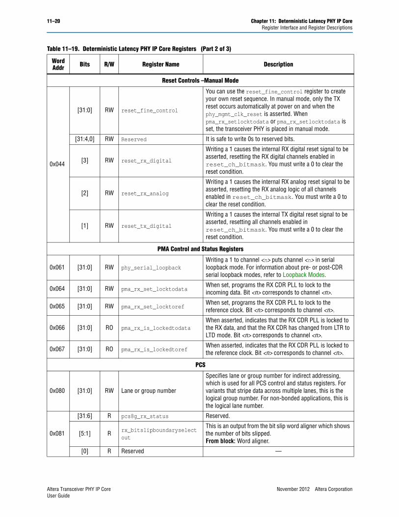
11–20 Chapter 11: Deterministic Latency PHY IP CoreRegister Interface and Register Descriptions
Reset Controls –Manual Mode
0x044
[31:0] RW reset_fine_control
You can use the reset_fine_control register to create your own reset sequence. In manual mode, only the TX reset occurs automatically at power on and when the phy_mgmt_clk_reset is asserted. When pma_rx_setlocktodata or pma_rx_setlocktodata is set, the transceiver PHY is placed in manual mode.
[31:4,0] RW Reserved It is safe to write 0s to reserved bits.
[3] RW reset_rx_digital
Writing a 1 causes the internal RX digital reset signal to be asserted, resetting the RX digital channels enabled in reset_ch_bitmask. You must write a 0 to clear the reset condition.
[2] RW reset_rx_analog
Writing a 1 causes the internal RX analog reset signal to be asserted, resetting the RX analog logic of all channels enabled in reset_ch_bitmask. You must write a 0 to clear the reset condition.
[1] RW reset_tx_digital
Writing a 1 causes the internal TX digital reset signal to be asserted, resetting all channels enabled in reset_ch_bitmask. You must write a 0 to clear the reset condition.
PMA Control and Status Registers
0x061 [31:0] RW phy_serial_loopbackWriting a 1 to channel <n> puts channel <n> in serial loopback mode. For information about pre- or post-CDR serial loopback modes, refer to Loopback Modes.
0x064 [31:0] RW pma_rx_set_locktodataWhen set, programs the RX CDR PLL to lock to the incoming data. Bit <n> corresponds to channel <n>.
0x065 [31:0] RW pma_rx_set_locktorefWhen set, programs the RX CDR PLL to lock to the reference clock. Bit <n> corresponds to channel <n>.
0x066 [31:0] RO pma_rx_is_lockedtodataWhen asserted, indicates that the RX CDR PLL is locked to the RX data, and that the RX CDR has changed from LTR to LTD mode. Bit <n> corresponds to channel <n>.
0x067 [31:0] RO pma_rx_is_lockedtorefWhen asserted, indicates that the RX CDR PLL is locked to the reference clock. Bit <n> corresponds to channel <n>.
PCS
0x080 [31:0] RW Lane or group number
Specifies lane or group number for indirect addressing, which is used for all PCS control and status registers. For variants that stripe data across multiple lanes, this is the logical group number. For non-bonded applications, this is the logical lane number.
0x081
[31:6] R pcs8g_rx_status Reserved.
[5:1] R rx_bitslipboundaryselectout
This is an output from the bit slip word aligner which shows the number of bits slipped.From block: Word aligner.
[0] R Reserved —
Table 11–19. Deterministic Latency PHY IP Core Registers (Part 2 of 3)
Word Addr Bits R/W Register Name Description
Altera Transceiver PHY IP Core November 2012 Altera CorporationUser Guide
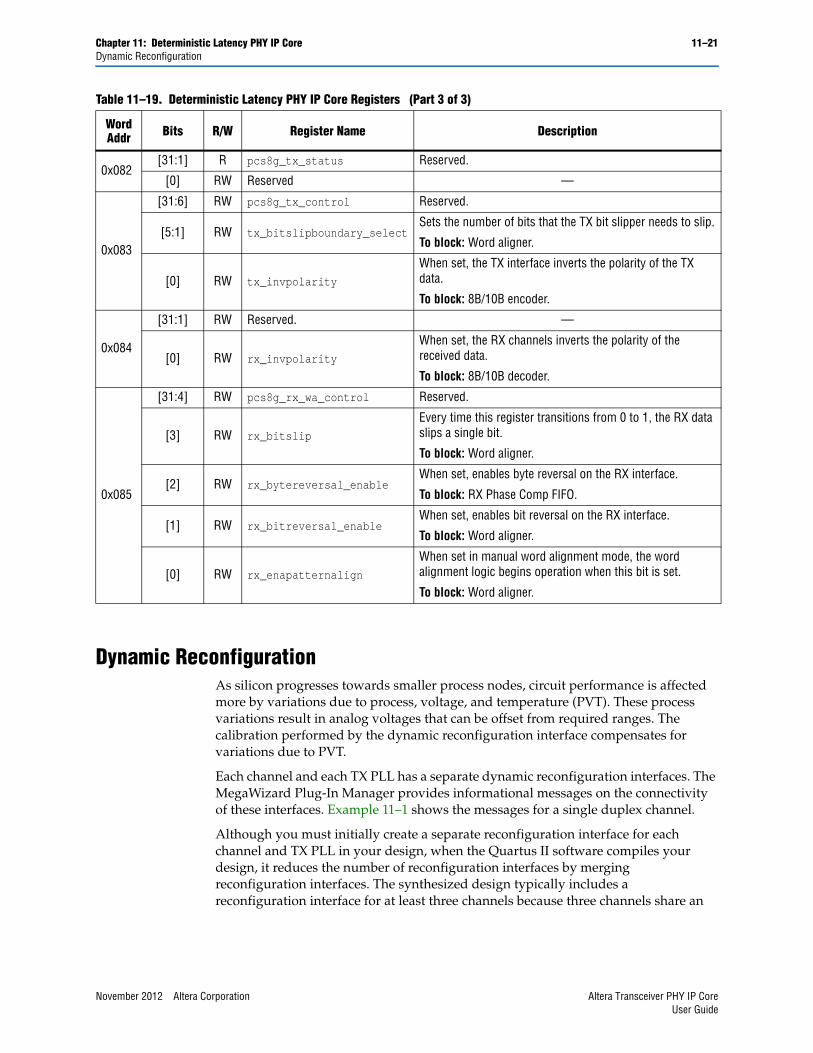
Chapter 11: Deterministic Latency PHY IP Core 11–21Dynamic Reconfiguration
Dynamic ReconfigurationAs silicon progresses towards smaller process nodes, circuit performance is affected more by variations due to process, voltage, and temperature (PVT). These process variations result in analog voltages that can be offset from required ranges. The calibration performed by the dynamic reconfiguration interface compensates for variations due to PVT.
Each channel and each TX PLL has a separate dynamic reconfiguration interfaces. The MegaWizard Plug-In Manager provides informational messages on the connectivity of these interfaces. Example 11–1 shows the messages for a single duplex channel.
Although you must initially create a separate reconfiguration interface for each channel and TX PLL in your design, when the Quartus II software compiles your design, it reduces the number of reconfiguration interfaces by merging reconfiguration interfaces. The synthesized design typically includes a reconfiguration interface for at least three channels because three channels share an
0x082[31:1] R pcs8g_tx_status Reserved.
[0] RW Reserved —
0x083
[31:6] RW pcs8g_tx_control Reserved.
[5:1] RW tx_bitslipboundary_selectSets the number of bits that the TX bit slipper needs to slip.
To block: Word aligner.
[0] RW tx_invpolarity
When set, the TX interface inverts the polarity of the TX data.
To block: 8B/10B encoder.
0x084
[31:1] RW Reserved. —
[0] RW rx_invpolarity
When set, the RX channels inverts the polarity of the received data.
To block: 8B/10B decoder.
0x085
[31:4] RW pcs8g_rx_wa_control Reserved.
[3] RW rx_bitslip
Every time this register transitions from 0 to 1, the RX data slips a single bit.
To block: Word aligner.
[2] RW rx_bytereversal_enableWhen set, enables byte reversal on the RX interface.
To block: RX Phase Comp FIFO.
[1] RW rx_bitreversal_enableWhen set, enables bit reversal on the RX interface.
To block: Word aligner.
[0] RW rx_enapatternalign
When set in manual word alignment mode, the word alignment logic begins operation when this bit is set.
To block: Word aligner.
Table 11–19. Deterministic Latency PHY IP Core Registers (Part 3 of 3)
Word Addr Bits R/W Register Name Description
November 2012 Altera Corporation Altera Transceiver PHY IP CoreUser Guide
11–22 Chapter 11: Deterministic Latency PHY IP CoreChannel Placement and Utilization
Avalon-MM slave interface which connects to the Transceiver Reconfiguration Controller IP Core. Conversely, you cannot connect the three channels that share an Avalon-MM interface to different Transceiver Reconfiguration Controller IP Cores. Doing so causes a Fitter error. For more information, refer to Transceiver Reconfiguration Controller to PHY IP Connectivity.
Table 11–20 describes the signals in the reconfiguration interface. This interface uses the Avalon-MM PHY Management interface clock.
Channel Placement and UtilizationThe Deterministic Latency PHY IP Core has the following restriction on channel placement:
■ Channels 0–2 in transceiver banks GXB_L0 and GSB_R0 of Arria V devices are not available for deterministic latency protocols.
Example 11–1. Informational Messages for the Transceiver Reconfiguration Interface
PHY IP will require 2 reconfiguration interfaces for connection to the external reconfiguration controller.Reconfiguration interface offset 0 is connected to the transceiver channel.Reconfiguration interface offset 1 is connected to the transmit PLL.
Table 11–20. Reconfiguration Interface
Signal Name Direction Description
reconfig_to_xcvr [(<n>70)-1:0] InputReconfiguration signals from the Transceiver Reconfiguration Controller. <n> grows linearly with the number of reconfiguration interfaces.
reconfig_from_xcvr[(<n>46)-1:0] OutputReconfiguration signals to the Transceiver Reconfiguration Controller. <n> grows linearly with the number of reconfiguration interfaces.
Altera Transceiver PHY IP Core November 2012 Altera CorporationUser Guide
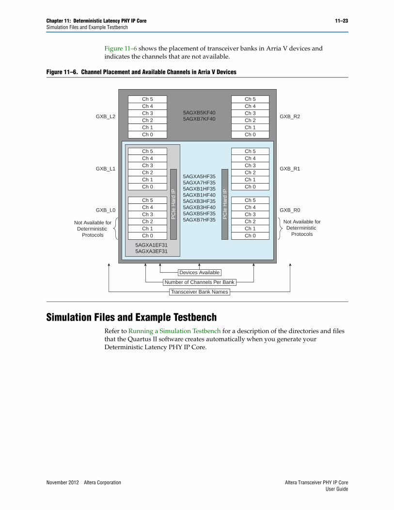
Chapter 11: Deterministic Latency PHY IP Core 11–23Simulation Files and Example Testbench
Figure 11–6 shows the placement of transceiver banks in Arria V devices and indicates the channels that are not available.
Simulation Files and Example Testbench Refer to Running a Simulation Testbench for a description of the directories and files that the Quartus II software creates automatically when you generate your Deterministic Latency PHY IP Core.
Figure 11–6. Channel Placement and Available Channels in Arria V Devices
GXB_R0
GXB_R1
GXB_L0
GXB_L1
GXB_R2GXB_L2
Devices Available
Number of Channels Per Bank
Transceiver Bank Names
5AGXB5KF405AGXB7KF40
5AGXA5HF355AGXA7HF355AGXB1HF355AGXB1HF405AGXB3HF355AGXB3HF405AGXB5HF355AGXB7HF35
5AGXA1EF315AGXA3EF31
PC
Ie H
ard
IP
PC
Ie H
ard
IP
Ch 5Ch 4Ch 3Ch 2Ch 1Ch 0 Ch 0
Ch 1Ch 2Ch 3Ch 4Ch 5
Ch 5Ch 4Ch 3Ch 2Ch 1Ch 0 Ch 0
Ch 1Ch 2Ch 3Ch 4Ch 5
Ch 5Ch 4Ch 3Ch 2Ch 1Ch 0 Ch 0
Ch 1Ch 2Ch 3Ch 4Ch 5
Not Available forDeterministic
Protocols
Not Available forDeterministic
Protocols
November 2012 Altera Corporation Altera Transceiver PHY IP CoreUser Guide

11–24 Chapter 11: Deterministic Latency PHY IP CoreSimulation Files and Example Testbench
Altera Transceiver PHY IP Core November 2012 Altera CorporationUser Guide
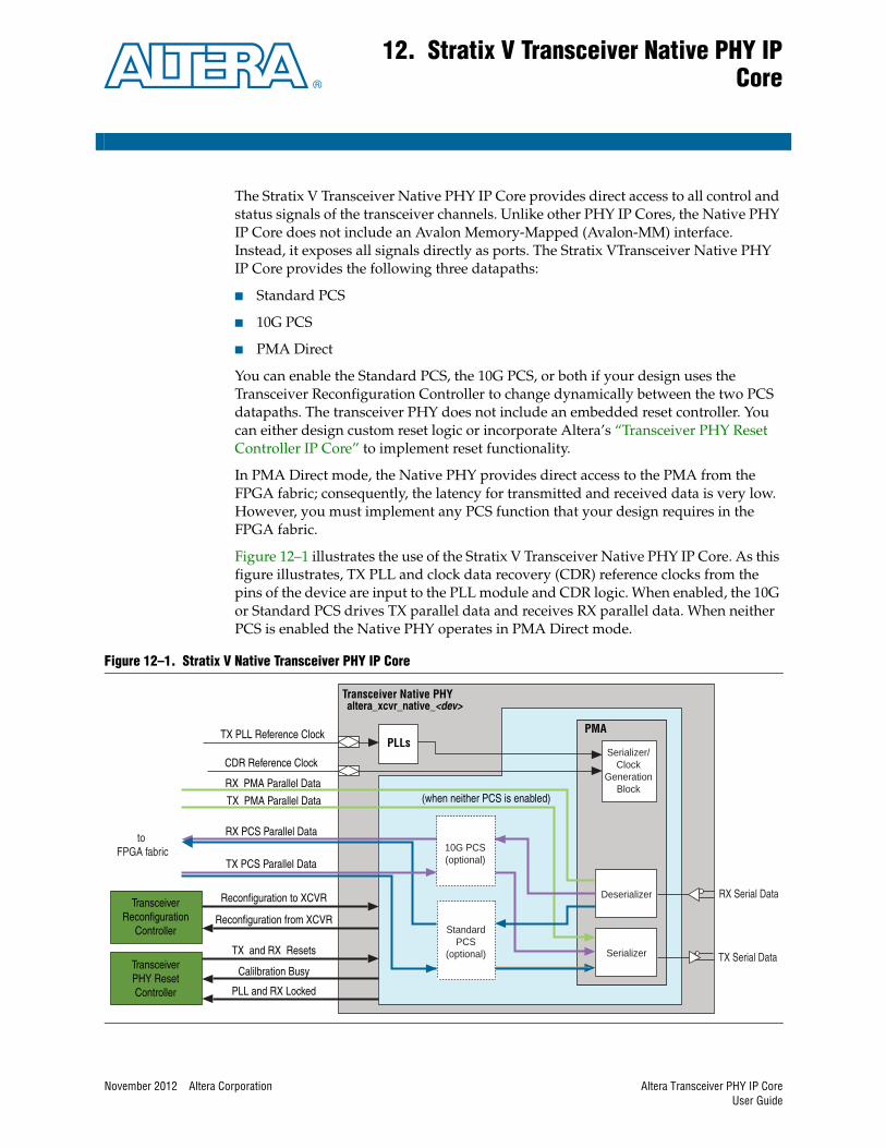
November 2012 Altera Corporation
12. Stratix V Transceiver Native PHY IPCore
The Stratix V Transceiver Native PHY IP Core provides direct access to all control and status signals of the transceiver channels. Unlike other PHY IP Cores, the Native PHY IP Core does not include an Avalon Memory-Mapped (Avalon-MM) interface. Instead, it exposes all signals directly as ports. The Stratix VTransceiver Native PHY IP Core provides the following three datapaths:
■ Standard PCS
■ 10G PCS
■ PMA Direct
You can enable the Standard PCS, the 10G PCS, or both if your design uses the Transceiver Reconfiguration Controller to change dynamically between the two PCS datapaths. The transceiver PHY does not include an embedded reset controller. You can either design custom reset logic or incorporate Altera’s “Transceiver PHY Reset Controller IP Core” to implement reset functionality.
In PMA Direct mode, the Native PHY provides direct access to the PMA from the FPGA fabric; consequently, the latency for transmitted and received data is very low. However, you must implement any PCS function that your design requires in the FPGA fabric.
Figure 12–1 illustrates the use of the Stratix V Transceiver Native PHY IP Core. As this figure illustrates, TX PLL and clock data recovery (CDR) reference clocks from the pins of the device are input to the PLL module and CDR logic. When enabled, the 10G or Standard PCS drives TX parallel data and receives RX parallel data. When neither PCS is enabled the Native PHY operates in PMA Direct mode.
Figure 12–1. Stratix V Native Transceiver PHY IP Core
PLLsPMA
altera_xcvr_native_<dev>Transceiver Native PHY
TransceiverReconfiguration
Controller
Reconfiguration to XCVR
Reconfiguration from XCVR
TX and RX Resets
Calilbration Busy
PLL and RX Locked
RX PCS Parallel Data
TX PCS Parallel Data
CDR Reference Clock
(when neither PCS is enabled)
TX PLL Reference Clock
Serializer/Clock
GenerationBlock
RX Serial Data
to FPGA fabric
TransceiverPHY ResetController
TX PMA Parallel Data
RX PMA Parallel Data
TX Serial DataSerializer
Deserializer
StandardPCS
(optional)
10G PCS(optional)
Altera Transceiver PHY IP CoreUser Guide
12–2 Chapter 12: Stratix V Transceiver Native PHY IP CoreDevice Family Support
In a typical design, the separately instantiated Transceiver PHY Reset Controller drives reset signals to Native PHY and receives calibration and locked status signal from the Native PHY. The Native PHY reconfiguration buses connect the external Transceiver Reconfiguration Controller for calibration and dynamic reconfiguration of the PLLs.
You specify the initial configuration when you parameterize the IP core. The Transceiver Native PHY IP Core connects to the “Transceiver Reconfiguration Controller IP Core” to dynamically change reference clocks and PLL connectivity at runtime.
Device Family SupportIP cores provide either final or preliminary support for target Altera device families. These terms have the following definitions:
■ Final support—Verified with final timing models for this device.
■ Preliminary support—Verified with preliminary timing models for this device.
Table 12–1 shows the level of support offered by the Stratix V Transceiver Native PHY IP Core for Altera device families.
Performance and Resource UtilizationBecause the 10G PCS, Standard PCS, and PMA are implemented in hard logic, the Stratix V Native PHY IP Core uses less than 1% of the available ALMs, memory, primary and secondary logic registers.
Table 12–1. Device Family Support
Device Family Support
Stratix V devices Preliminary
Other device families No support
Altera Transceiver PHY IP Core November 2012 Altera CorporationUser Guide
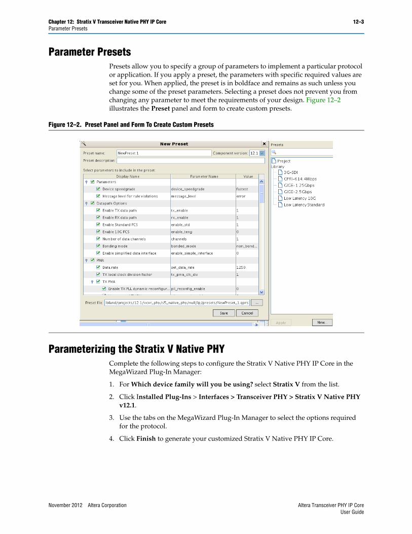
Chapter 12: Stratix V Transceiver Native PHY IP Core 12–3Parameter Presets
Parameter PresetsPresets allow you to specify a group of parameters to implement a particular protocol or application. If you apply a preset, the parameters with specific required values are set for you. When applied, the preset is in boldface and remains as such unless you change some of the preset parameters. Selecting a preset does not prevent you from changing any parameter to meet the requirements of your design. Figure 12–2 illustrates the Preset panel and form to create custom presets.
Parameterizing the Stratix V Native PHYComplete the following steps to configure the Stratix V Native PHY IP Core in the MegaWizard Plug-In Manager:
1. For Which device family will you be using? select Stratix V from the list.
2. Click Installed Plug-Ins > Interfaces > Transceiver PHY > Stratix V Native PHY v12.1.
3. Use the tabs on the MegaWizard Plug-In Manager to select the options required for the protocol.
4. Click Finish to generate your customized Stratix V Native PHY IP Core.
Figure 12–2. Preset Panel and Form To Create Custom Presets
November 2012 Altera Corporation Altera Transceiver PHY IP CoreUser Guide
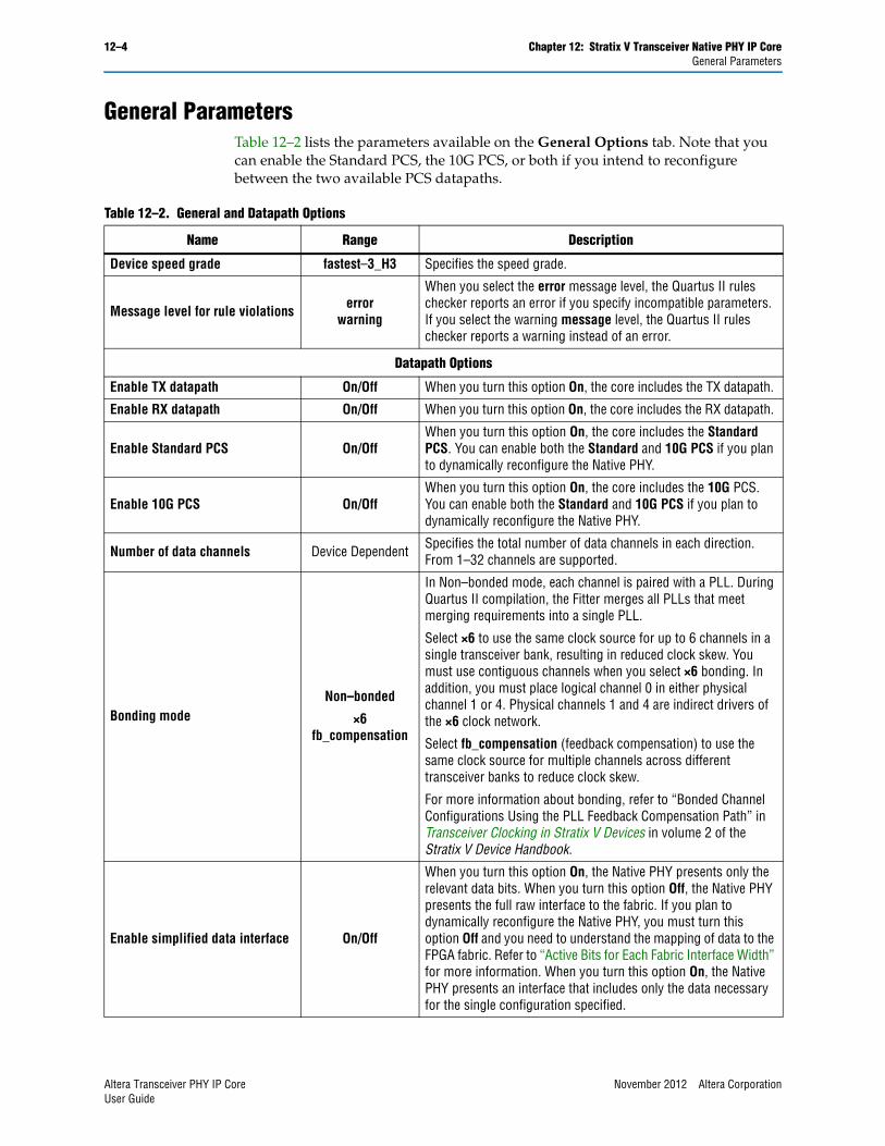
12–4 Chapter 12: Stratix V Transceiver Native PHY IP CoreGeneral Parameters
General ParametersTable 12–2 lists the parameters available on the General Options tab. Note that you can enable the Standard PCS, the 10G PCS, or both if you intend to reconfigure between the two available PCS datapaths.
Table 12–2. General and Datapath Options
Name Range Description
Device speed grade fastest–3_H3 Specifies the speed grade.
Message level for rule violations errorwarning
When you select the error message level, the Quartus II rules checker reports an error if you specify incompatible parameters. If you select the warning message level, the Quartus II rules checker reports a warning instead of an error.
Datapath Options
Enable TX datapath On/Off When you turn this option On, the core includes the TX datapath.
Enable RX datapath On/Off When you turn this option On, the core includes the RX datapath.
Enable Standard PCS On/OffWhen you turn this option On, the core includes the Standard PCS. You can enable both the Standard and 10G PCS if you plan to dynamically reconfigure the Native PHY.
Enable 10G PCS On/OffWhen you turn this option On, the core includes the 10G PCS. You can enable both the Standard and 10G PCS if you plan to dynamically reconfigure the Native PHY.
Number of data channels Device Dependent Specifies the total number of data channels in each direction. From 1–32 channels are supported.
Bonding modeNon–bonded
×6fb_compensation
In Non–bonded mode, each channel is paired with a PLL. During Quartus II compilation, the Fitter merges all PLLs that meet merging requirements into a single PLL.
Select ×6 to use the same clock source for up to 6 channels in a single transceiver bank, resulting in reduced clock skew. You must use contiguous channels when you select ×6 bonding. In addition, you must place logical channel 0 in either physical channel 1 or 4. Physical channels 1 and 4 are indirect drivers of the ×6 clock network.
Select fb_compensation (feedback compensation) to use the same clock source for multiple channels across different transceiver banks to reduce clock skew.
For more information about bonding, refer to “Bonded Channel Configurations Using the PLL Feedback Compensation Path” in Transceiver Clocking in Stratix V Devices in volume 2 of the Stratix V Device Handbook.
Enable simplified data interface On/Off
When you turn this option On, the Native PHY presents only the relevant data bits. When you turn this option Off, the Native PHY presents the full raw interface to the fabric. If you plan to dynamically reconfigure the Native PHY, you must turn this option Off and you need to understand the mapping of data to the FPGA fabric. Refer to “Active Bits for Each Fabric Interface Width” for more information. When you turn this option On, the Native PHY presents an interface that includes only the data necessary for the single configuration specified.
Altera Transceiver PHY IP Core November 2012 Altera CorporationUser Guide
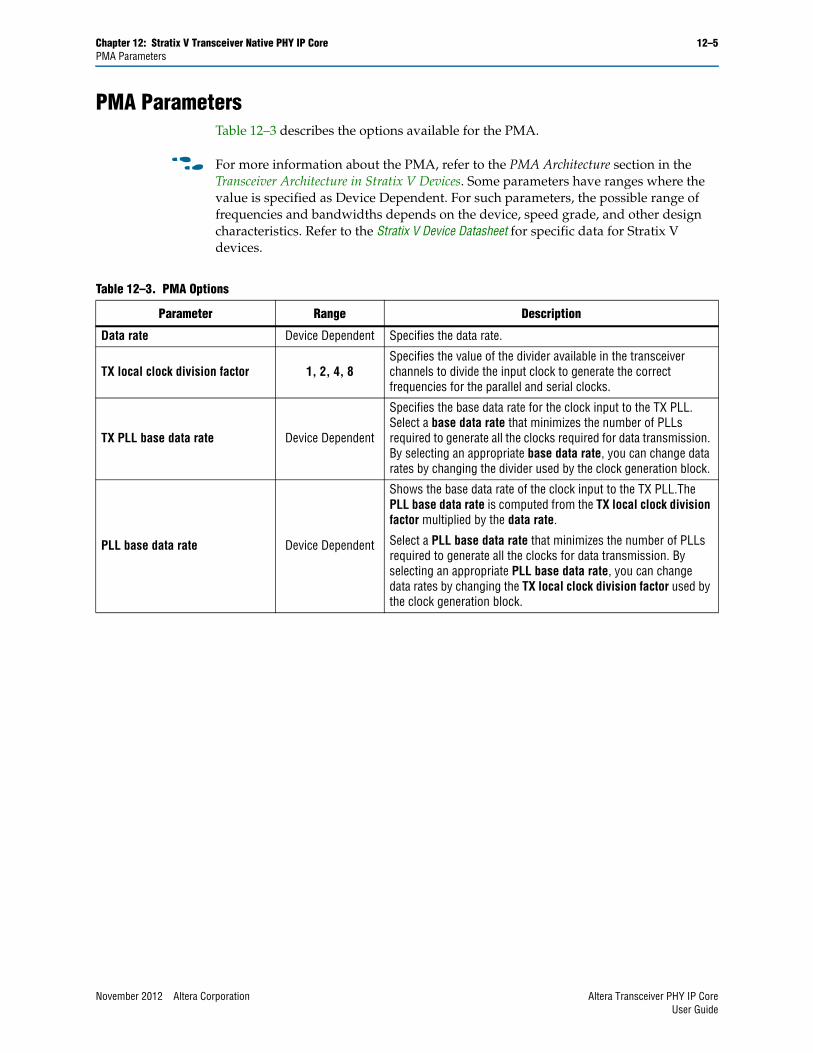
Chapter 12: Stratix V Transceiver Native PHY IP Core 12–5PMA Parameters
PMA ParametersTable 12–3 describes the options available for the PMA.
f For more information about the PMA, refer to the PMA Architecture section in the Transceiver Architecture in Stratix V Devices. Some parameters have ranges where the value is specified as Device Dependent. For such parameters, the possible range of frequencies and bandwidths depends on the device, speed grade, and other design characteristics. Refer to the Stratix V Device Datasheet for specific data for Stratix V devices.
Table 12–3. PMA Options
Parameter Range Description
Data rate Device Dependent Specifies the data rate.
TX local clock division factor 1, 2, 4, 8Specifies the value of the divider available in the transceiver channels to divide the input clock to generate the correct frequencies for the parallel and serial clocks.
TX PLL base data rate Device Dependent
Specifies the base data rate for the clock input to the TX PLL. Select a base data rate that minimizes the number of PLLs required to generate all the clocks required for data transmission. By selecting an appropriate base data rate, you can change data rates by changing the divider used by the clock generation block.
PLL base data rate Device Dependent
Shows the base data rate of the clock input to the TX PLL.The PLL base data rate is computed from the TX local clock division factor multiplied by the data rate.
Select a PLL base data rate that minimizes the number of PLLs required to generate all the clocks for data transmission. By selecting an appropriate PLL base data rate, you can change data rates by changing the TX local clock division factor used by the clock generation block.
November 2012 Altera Corporation Altera Transceiver PHY IP CoreUser Guide
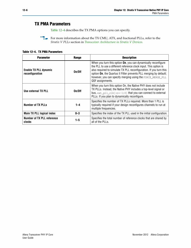
12–6 Chapter 12: Stratix V Transceiver Native PHY IP CorePMA Parameters
TX PMA ParametersTable 12–4 describes the TX PMA options you can specify.
f For more information about the TX CMU, ATX, and fractional PLLs, refer to the Stratix V PLLs section in Transceiver Architecture in Stratix V Devices.
Table 12–4. TX PMA Parameters
Parameter Range Description
Enable TX PLL dynamic reconfiguration On/Off
When you turn this option On, you can dynamically reconfigure the PLL to use a different reference clock input. This option is also required to simulate TX PLL reconfiguration. If you turn this option On, the Quartus II Fitter prevents PLL merging by default; however, you can specify merging using the FORCE_MERGE_PLL QSF assignments.
Use external TX PLL On/Off
When you turn this option On, the Native PHY does not include TX PLLs. Instead, the Native PHY includes a top-level signal or bus, ext_pll_clk[<n>-1:0] that you can connect to external PLLs. If you plan to dynamically reconfigure.
Number of TX PLLs 1–4Specifies the number of TX PLLs required. More than 1 PLL is typically required if your design reconfigures channels to run at multiple frequencies.
Main TX PLL logical index 0–3 Specifies the index of the TX PLL used in the initial configuration.
Number of TX PLL reference clocks 1–5 Specifies the total number of reference clocks that are shared by
all of the PLLs.
Altera Transceiver PHY IP Core November 2012 Altera CorporationUser Guide
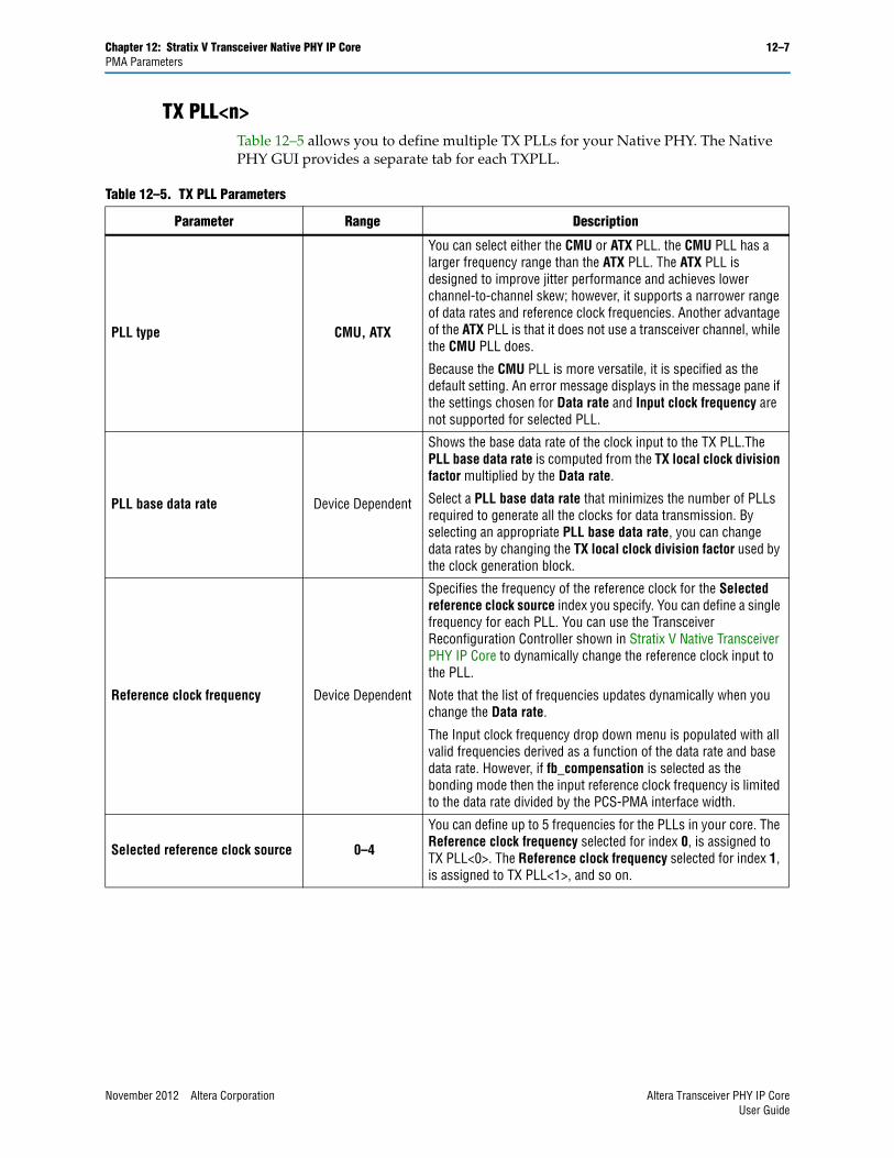
Chapter 12: Stratix V Transceiver Native PHY IP Core 12–7PMA Parameters
TX PLL<n>Table 12–5 allows you to define multiple TX PLLs for your Native PHY. The Native PHY GUI provides a separate tab for each TXPLL.
Table 12–5. TX PLL Parameters
Parameter Range Description
PLL type CMU, ATX
You can select either the CMU or ATX PLL. the CMU PLL has a larger frequency range than the ATX PLL. The ATX PLL is designed to improve jitter performance and achieves lower channel-to-channel skew; however, it supports a narrower range of data rates and reference clock frequencies. Another advantage of the ATX PLL is that it does not use a transceiver channel, while the CMU PLL does.
Because the CMU PLL is more versatile, it is specified as the default setting. An error message displays in the message pane if the settings chosen for Data rate and Input clock frequency are not supported for selected PLL.
PLL base data rate Device Dependent
Shows the base data rate of the clock input to the TX PLL.The PLL base data rate is computed from the TX local clock division factor multiplied by the Data rate.
Select a PLL base data rate that minimizes the number of PLLs required to generate all the clocks for data transmission. By selecting an appropriate PLL base data rate, you can change data rates by changing the TX local clock division factor used by the clock generation block.
Reference clock frequency Device Dependent
Specifies the frequency of the reference clock for the Selected reference clock source index you specify. You can define a single frequency for each PLL. You can use the Transceiver Reconfiguration Controller shown in Stratix V Native Transceiver PHY IP Core to dynamically change the reference clock input to the PLL.
Note that the list of frequencies updates dynamically when you change the Data rate.
The Input clock frequency drop down menu is populated with all valid frequencies derived as a function of the data rate and base data rate. However, if fb_compensation is selected as the bonding mode then the input reference clock frequency is limited to the data rate divided by the PCS-PMA interface width.
Selected reference clock source 0–4
You can define up to 5 frequencies for the PLLs in your core. The Reference clock frequency selected for index 0, is assigned to TX PLL<0>. The Reference clock frequency selected for index 1, is assigned to TX PLL<1>, and so on.
November 2012 Altera Corporation Altera Transceiver PHY IP CoreUser Guide
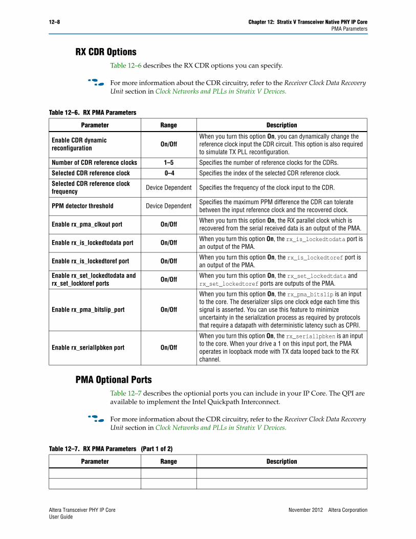
12–8 Chapter 12: Stratix V Transceiver Native PHY IP CorePMA Parameters
RX CDR OptionsTable 12–6 describes the RX CDR options you can specify.
f For more information about the CDR circuitry, refer to the Receiver Clock Data Recovery Unit section in Clock Networks and PLLs in Stratix V Devices.
PMA Optional PortsTable 12–7 describes the optionial ports you can include in your IP Core. The QPI are available to implement the Intel Quickpath Interconnect.
f For more information about the CDR circuitry, refer to the Receiver Clock Data Recovery Unit section in Clock Networks and PLLs in Stratix V Devices.
Table 12–6. RX PMA Parameters
Parameter Range Description
Enable CDR dynamic reconfiguration On/Off
When you turn this option On, you can dynamically change the reference clock input the CDR circuit. This option is also required to simulate TX PLL reconfiguration.
Number of CDR reference clocks 1–5 Specifies the number of reference clocks for the CDRs.
Selected CDR reference clock 0–4 Specifies the index of the selected CDR reference clock.
Selected CDR reference clock frequency Device Dependent Specifies the frequency of the clock input to the CDR.
PPM detector threshold Device Dependent Specifies the maximum PPM difference the CDR can tolerate between the input reference clock and the recovered clock.
Enable rx_pma_clkout port On/Off When you turn this option On, the RX parallel clock which is recovered from the serial received data is an output of the PMA.
Enable rx_is_lockedtodata port On/Off When you turn this option On, the rx_is_lockedtodata port is an output of the PMA.
Enable rx_is_lockedtoref port On/Off When you turn this option On, the rx_is_lockedtoref port is an output of the PMA.
Enable rx_set_lockedtodata and rx_set_locktoref ports On/Off When you turn this option On, the rx_set_lockedtdata and
rx_set_lockedtoref ports are outputs of the PMA.
Enable rx_pma_bitslip_port On/Off
When you turn this option On, the rx_pma_bitslip is an input to the core. The deserializer slips one clock edge each time this signal is asserted. You can use this feature to minimize uncertainty in the serialization process as required by protocols that require a datapath with deterministic latency such as CPRI.
Enable rx_seriallpbken port On/Off
When you turn this option On, the rx_seriallpbken is an input to the core. When your drive a 1 on this input port, the PMA operates in loopback mode with TX data looped back to the RX channel.
Table 12–7. RX PMA Parameters (Part 1 of 2)
Parameter Range Description
Altera Transceiver PHY IP Core November 2012 Altera CorporationUser Guide
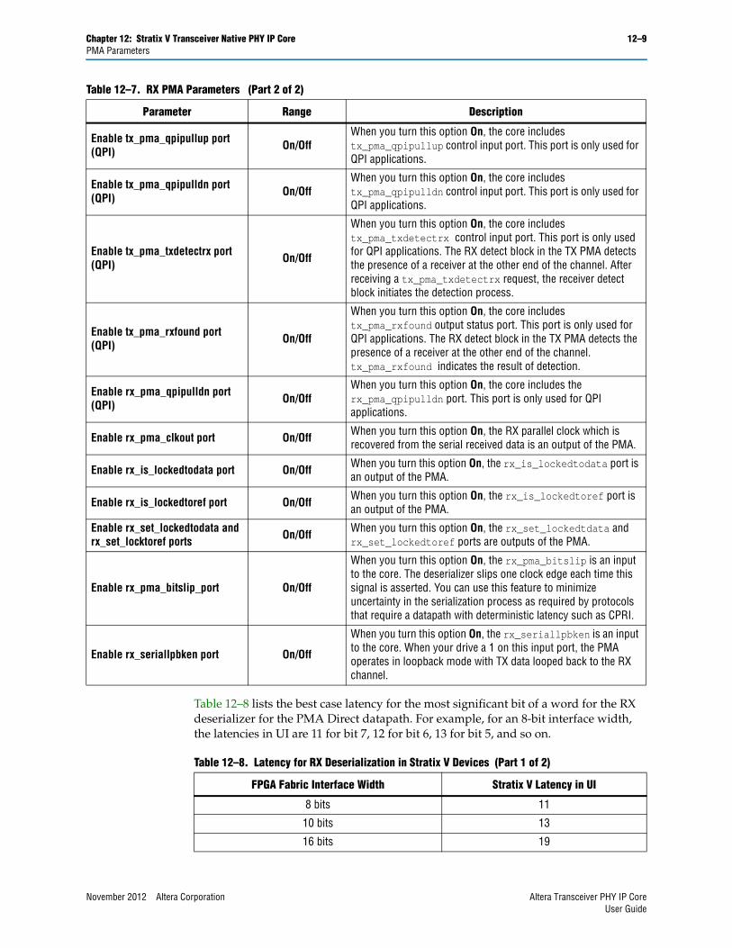
Chapter 12: Stratix V Transceiver Native PHY IP Core 12–9PMA Parameters
Table 12–8 lists the best case latency for the most significant bit of a word for the RX deserializer for the PMA Direct datapath. For example, for an 8-bit interface width, the latencies in UI are 11 for bit 7, 12 for bit 6, 13 for bit 5, and so on.
Enable tx_pma_qpipullup port (QPI) On/Off
When you turn this option On, the core includes tx_pma_qpipullup control input port. This port is only used for QPI applications.
Enable tx_pma_qpipulldn port (QPI) On/Off
When you turn this option On, the core includes tx_pma_qpipulldn control input port. This port is only used for QPI applications.
Enable tx_pma_txdetectrx port (QPI) On/Off
When you turn this option On, the core includes tx_pma_txdetectrx control input port. This port is only used for QPI applications. The RX detect block in the TX PMA detects the presence of a receiver at the other end of the channel. After receiving a tx_pma_txdetectrx request, the receiver detect block initiates the detection process.
Enable tx_pma_rxfound port (QPI) On/Off
When you turn this option On, the core includes tx_pma_rxfound output status port. This port is only used for QPI applications. The RX detect block in the TX PMA detects the presence of a receiver at the other end of the channel. tx_pma_rxfound indicates the result of detection.
Enable rx_pma_qpipulldn port (QPI) On/Off
When you turn this option On, the core includes the rx_pma_qpipulldn port. This port is only used for QPI applications.
Enable rx_pma_clkout port On/Off When you turn this option On, the RX parallel clock which is recovered from the serial received data is an output of the PMA.
Enable rx_is_lockedtodata port On/Off When you turn this option On, the rx_is_lockedtodata port is an output of the PMA.
Enable rx_is_lockedtoref port On/Off When you turn this option On, the rx_is_lockedtoref port is an output of the PMA.
Enable rx_set_lockedtodata and rx_set_locktoref ports On/Off When you turn this option On, the rx_set_lockedtdata and
rx_set_lockedtoref ports are outputs of the PMA.
Enable rx_pma_bitslip_port On/Off
When you turn this option On, the rx_pma_bitslip is an input to the core. The deserializer slips one clock edge each time this signal is asserted. You can use this feature to minimize uncertainty in the serialization process as required by protocols that require a datapath with deterministic latency such as CPRI.
Enable rx_seriallpbken port On/Off
When you turn this option On, the rx_seriallpbken is an input to the core. When your drive a 1 on this input port, the PMA operates in loopback mode with TX data looped back to the RX channel.
Table 12–7. RX PMA Parameters (Part 2 of 2)
Parameter Range Description
Table 12–8. Latency for RX Deserialization in Stratix V Devices (Part 1 of 2)
FPGA Fabric Interface Width Stratix V Latency in UI
8 bits 11
10 bits 13
16 bits 19
November 2012 Altera Corporation Altera Transceiver PHY IP CoreUser Guide
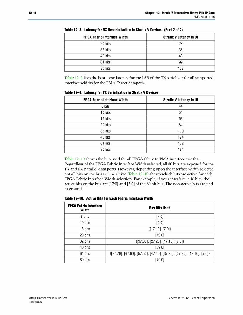
12–10 Chapter 12: Stratix V Transceiver Native PHY IP CorePMA Parameters
Table 12–9 lists the best- case latency for the LSB of the TX serializer for all supported interface widths for the PMA Direct datapath.
Table 12–10 shows the bits used for all FPGA fabric to PMA interface widths. Regardless of the FPGA Fabric Interface Width selected, all 80 bits are exposed for the TX and RX parallel data ports. However, depending upon the interface width selected not all bits on the bus will be active. Table 12–10 shows which bits are active for each FPGA Fabric Interface Width selection. For example, if your interface is 16 bits, the active bits on the bus are [17:0] and [7:0] of the 80 bit bus. The non-active bits are tied to ground.
20 bits 23
32 bits 35
40 bits 43
64 bits 99
80 bits 123
Table 12–9. Latency for TX Serialization in Stratix V Devices
FPGA Fabric Interface Width Stratix V Latency in UI
8 bits 44
10 bits 54
16 bits 68
20 bits 84
32 bits 100
40 bits 124
64 bits 132
80 bits 164
Table 12–10. Active Bits for Each Fabric Interface Width
FPGA Fabric Interface Width Bus Bits Used
8 bits [7:0]
10 bits [9:0]
16 bits {[17:10], [7:0]}
20 bits [19:0]
32 bits {[37:30], [27:20], [17:10], [7:0]}
40 bits [39:0]
64 bits {[77:70], [67:60], [57:50], [47:40], [37:30], [27:20], [17:10], [7:0]}
80 bits [79:0]
Table 12–8. Latency for RX Deserialization in Stratix V Devices (Part 2 of 2)
FPGA Fabric Interface Width Stratix V Latency in UI
Altera Transceiver PHY IP Core November 2012 Altera CorporationUser Guide
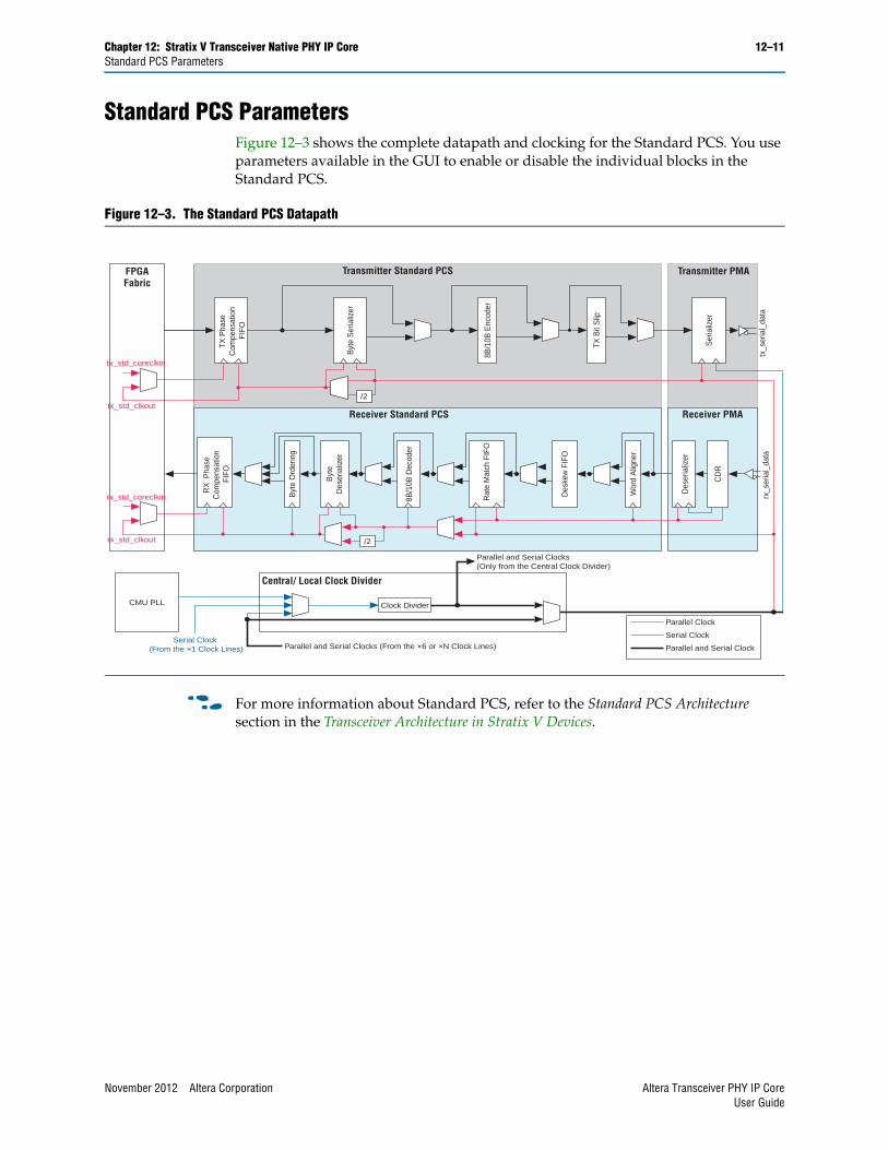
Chapter 12: Stratix V Transceiver Native PHY IP Core 12–11Standard PCS Parameters
Standard PCS ParametersFigure 12–3 shows the complete datapath and clocking for the Standard PCS. You use parameters available in the GUI to enable or disable the individual blocks in the Standard PCS.
f For more information about Standard PCS, refer to the Standard PCS Architecture section in the Transceiver Architecture in Stratix V Devices.
Figure 12–3. The Standard PCS Datapath R
X P
hase
C
ompe
nsat
ion
FIFO
Byt
e O
rder
ing
Byt
eD
eser
ializ
er
8B/1
0B D
ecod
er
Rat
e M
atch
FIF
O
Receiver Standard PCS Receiver PMA
Des
kew
FIF
O
Wor
d A
ligne
r
Des
eria
lizer
CD
R
Transmitter Standard PCS Transmitter PMA
Ser
ializ
er
tx_s
eria
l_da
tarx
_ser
ial_
data
FPGAFabric
TX P
hase
C
ompe
nsat
ion
FIFO
Byt
e S
eria
lizer
8B/1
0B E
ncod
er
TX B
it S
lip
/2
/2
Parallel Clock
Serial Clock
Parallel and Serial Clock
Clock Divider
Parallel and Serial Clocks (From the ×6 or ×N Clock Lines)Serial Clock
(From the ×1 Clock Lines)
Central/ Local Clock Divider
Parallel and Serial Clocks(Only from the Central Clock Divider)
CMU PLL
tx_std_coreclkin
rx_std_coreclkin
rx_std_clkout
tx_std_clkout
November 2012 Altera Corporation Altera Transceiver PHY IP CoreUser Guide
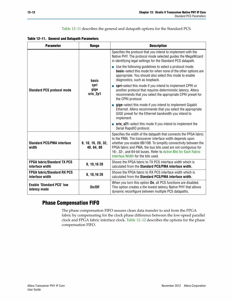
12–12 Chapter 12: Stratix V Transceiver Native PHY IP CoreStandard PCS Parameters
Table 12–11 describes the general and datapath options for the Standard PCS.
Phase Compensation FIFOThe phase compensation FIFO assures clean data transfer to and from the FPGA fabric by compensating for the clock phase difference between the low-speed parallel clock and FPGA fabric interface clock. Table 12–12 describes the options for the phase compensation FIFO.
Table 12–11. General and Datapath Parameters
Parameter Range Description
Standard PCS protocol mode
basiccprigige
srio_2p1
Specifies the protocol that you intend to implement with the Native PHY. The protocol mode selected guides the MegaWizard in identifying legal settings for the Standard PCS datapath.
■ Use the following guidelines to select a protocol mode: basic–select this mode for when none of the other options are appropriate. You should also select this mode to enable diagnostics, such as loopback.
■ cpri–select this mode if you intend to implement CPRI or another protocol that requires deterministic latency. Altera recommends that you select the appropriate CPRI preset for the CPRI protocol.
■ gige–select this mode if you intend to implement Gigabit Ethernet. Altera recommends that you select the appropriate GIGE preset for the Ethernet bandwidth you intend to implement.
■ srio_s21–select this mode if you intend to implement the Serial RapidIO protocol.
Standard PCS/PMA interface width
8, 10, 16, 20, 32, 40, 64, 80
Specifies the width of the datapath that connects the FPGA fabric to the PMA. The transceiver interface width depends upon whether you enable 8B/10B. To simplify connectivity between the FPGA fabric and PMA, the bus bits used are not contiguous for 16-, 32-, and 64-bit buses. Refer to Active Bits for Each Fabric Interface Width for the bits used.
FPGA fabric/Standard TX PCS interface width 8, 10,16 20 Shows the FPGA fabric to TX PCS interface width which is
calculated from the Standard PCS/PMA interface width.
FPGA fabric/Standard RX PCS interface width 8, 10,16 20 Shows the FPGA fabric to RX PCS interface width which is
calculated from the Standard PCS/PMA interface width.
Enable ‘Standard PCS’ low latency mode On/Off
When you turn this option On, all PCS functions are disabled. This option creates a the lowest latency Native PHY that allows dynamic reconfigure between multiple PCS datapaths.
Altera Transceiver PHY IP Core November 2012 Altera CorporationUser Guide
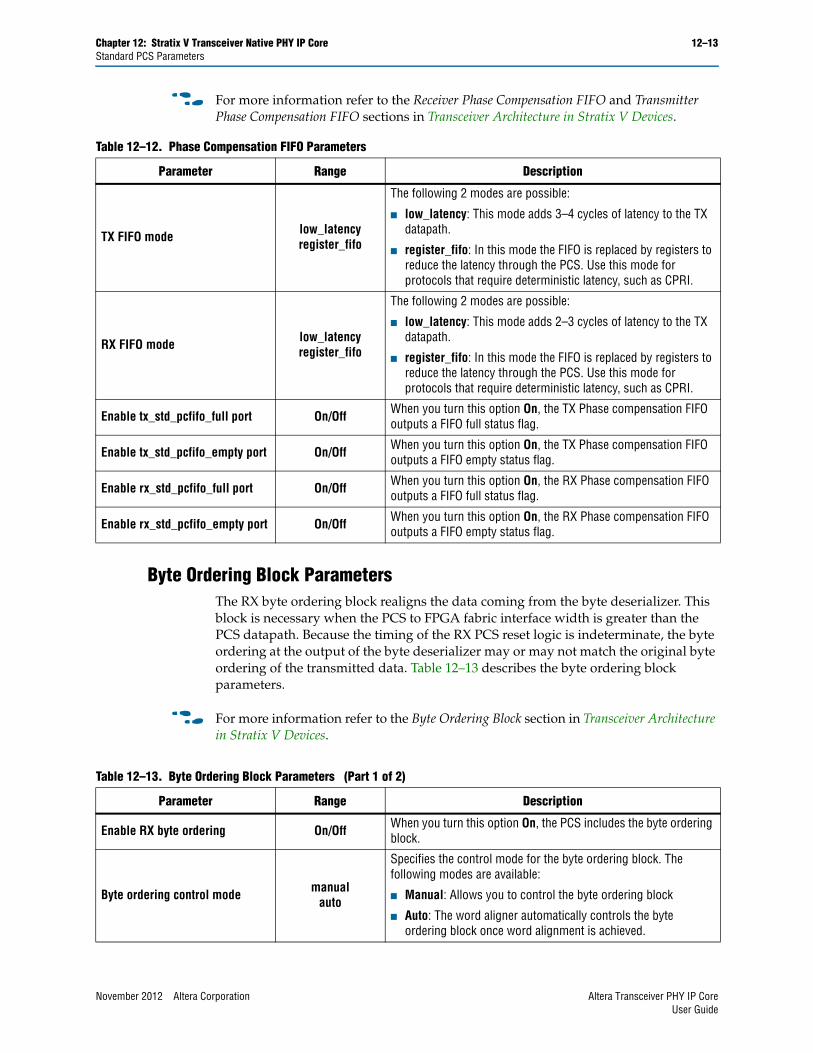
Chapter 12: Stratix V Transceiver Native PHY IP Core 12–13Standard PCS Parameters
f For more information refer to the Receiver Phase Compensation FIFO and Transmitter Phase Compensation FIFO sections in Transceiver Architecture in Stratix V Devices.
Byte Ordering Block ParametersThe RX byte ordering block realigns the data coming from the byte deserializer. This block is necessary when the PCS to FPGA fabric interface width is greater than the PCS datapath. Because the timing of the RX PCS reset logic is indeterminate, the byte ordering at the output of the byte deserializer may or may not match the original byte ordering of the transmitted data. Table 12–13 describes the byte ordering block parameters.
f For more information refer to the Byte Ordering Block section in Transceiver Architecture in Stratix V Devices.
Table 12–12. Phase Compensation FIFO Parameters
Parameter Range Description
TX FIFO mode low_latencyregister_fifo
The following 2 modes are possible:
■ low_latency: This mode adds 3–4 cycles of latency to the TX datapath.
■ register_fifo: In this mode the FIFO is replaced by registers to reduce the latency through the PCS. Use this mode for protocols that require deterministic latency, such as CPRI.
RX FIFO mode low_latencyregister_fifo
The following 2 modes are possible:
■ low_latency: This mode adds 2–3 cycles of latency to the TX datapath.
■ register_fifo: In this mode the FIFO is replaced by registers to reduce the latency through the PCS. Use this mode for protocols that require deterministic latency, such as CPRI.
Enable tx_std_pcfifo_full port On/Off When you turn this option On, the TX Phase compensation FIFO outputs a FIFO full status flag.
Enable tx_std_pcfifo_empty port On/Off When you turn this option On, the TX Phase compensation FIFO outputs a FIFO empty status flag.
Enable rx_std_pcfifo_full port On/Off When you turn this option On, the RX Phase compensation FIFO outputs a FIFO full status flag.
Enable rx_std_pcfifo_empty port On/Off When you turn this option On, the RX Phase compensation FIFO outputs a FIFO empty status flag.
Table 12–13. Byte Ordering Block Parameters (Part 1 of 2)
Parameter Range Description
Enable RX byte ordering On/Off When you turn this option On, the PCS includes the byte ordering block.
Byte ordering control mode manualauto
Specifies the control mode for the byte ordering block. The following modes are available:
■ Manual: Allows you to control the byte ordering block
■ Auto: The word aligner automatically controls the byte ordering block once word alignment is achieved.
November 2012 Altera Corporation Altera Transceiver PHY IP CoreUser Guide
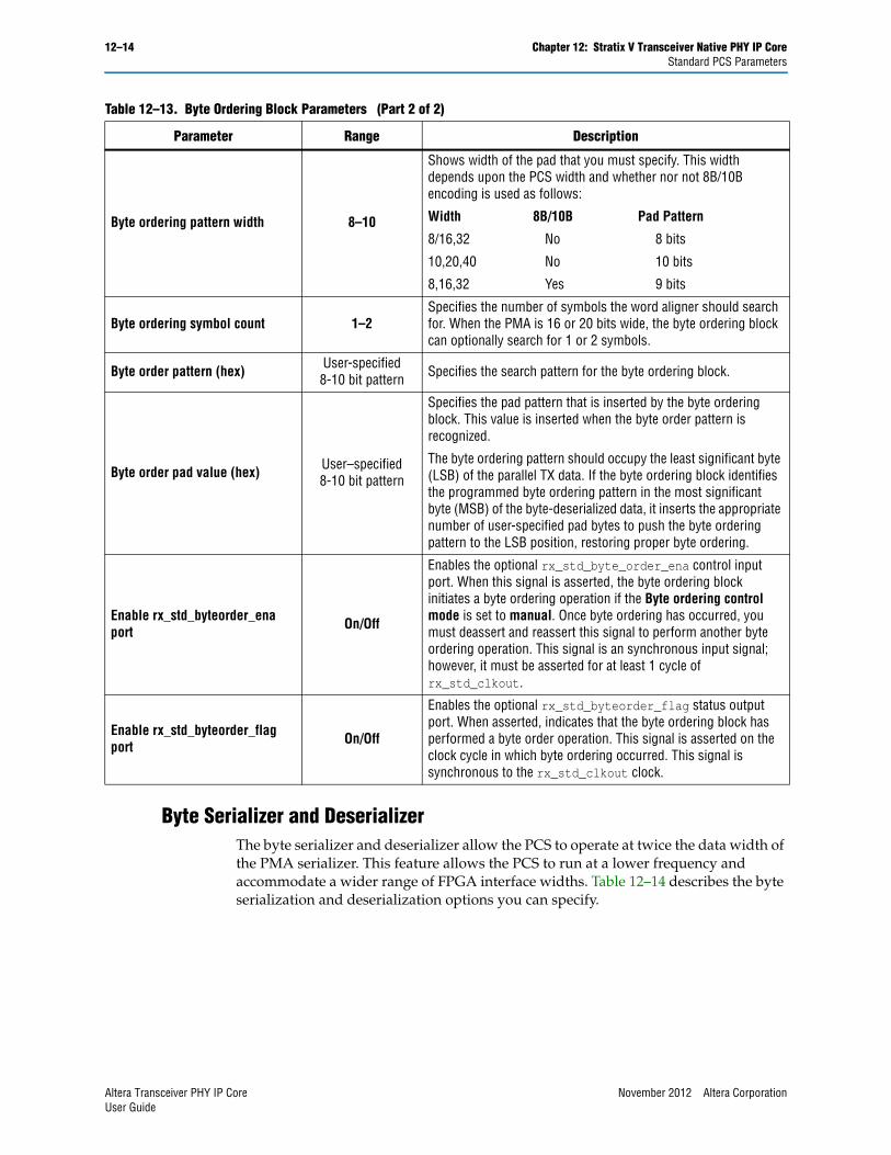
12–14 Chapter 12: Stratix V Transceiver Native PHY IP CoreStandard PCS Parameters
Byte Serializer and DeserializerThe byte serializer and deserializer allow the PCS to operate at twice the data width of the PMA serializer. This feature allows the PCS to run at a lower frequency and accommodate a wider range of FPGA interface widths. Table 12–14 describes the byte serialization and deserialization options you can specify.
Byte ordering pattern width 8–10
Shows width of the pad that you must specify. This width depends upon the PCS width and whether nor not 8B/10B encoding is used as follows:
Width 8B/10B Pad Pattern
8/16,32 No 8 bits
10,20,40 No 10 bits
8,16,32 Yes 9 bits
Byte ordering symbol count 1–2Specifies the number of symbols the word aligner should search for. When the PMA is 16 or 20 bits wide, the byte ordering block can optionally search for 1 or 2 symbols.
Byte order pattern (hex) User-specified 8-10 bit pattern Specifies the search pattern for the byte ordering block.
Byte order pad value (hex) User–specified 8-10 bit pattern
Specifies the pad pattern that is inserted by the byte ordering block. This value is inserted when the byte order pattern is recognized.
The byte ordering pattern should occupy the least significant byte (LSB) of the parallel TX data. If the byte ordering block identifies the programmed byte ordering pattern in the most significant byte (MSB) of the byte-deserialized data, it inserts the appropriate number of user-specified pad bytes to push the byte ordering pattern to the LSB position, restoring proper byte ordering.
Enable rx_std_byteorder_ena port On/Off
Enables the optional rx_std_byte_order_ena control input port. When this signal is asserted, the byte ordering block initiates a byte ordering operation if the Byte ordering control mode is set to manual. Once byte ordering has occurred, you must deassert and reassert this signal to perform another byte ordering operation. This signal is an synchronous input signal; however, it must be asserted for at least 1 cycle of rx_std_clkout.
Enable rx_std_byteorder_flag port On/Off
Enables the optional rx_std_byteorder_flag status output port. When asserted, indicates that the byte ordering block has performed a byte order operation. This signal is asserted on the clock cycle in which byte ordering occurred. This signal is synchronous to the rx_std_clkout clock.
Table 12–13. Byte Ordering Block Parameters (Part 2 of 2)
Parameter Range Description
Altera Transceiver PHY IP Core November 2012 Altera CorporationUser Guide
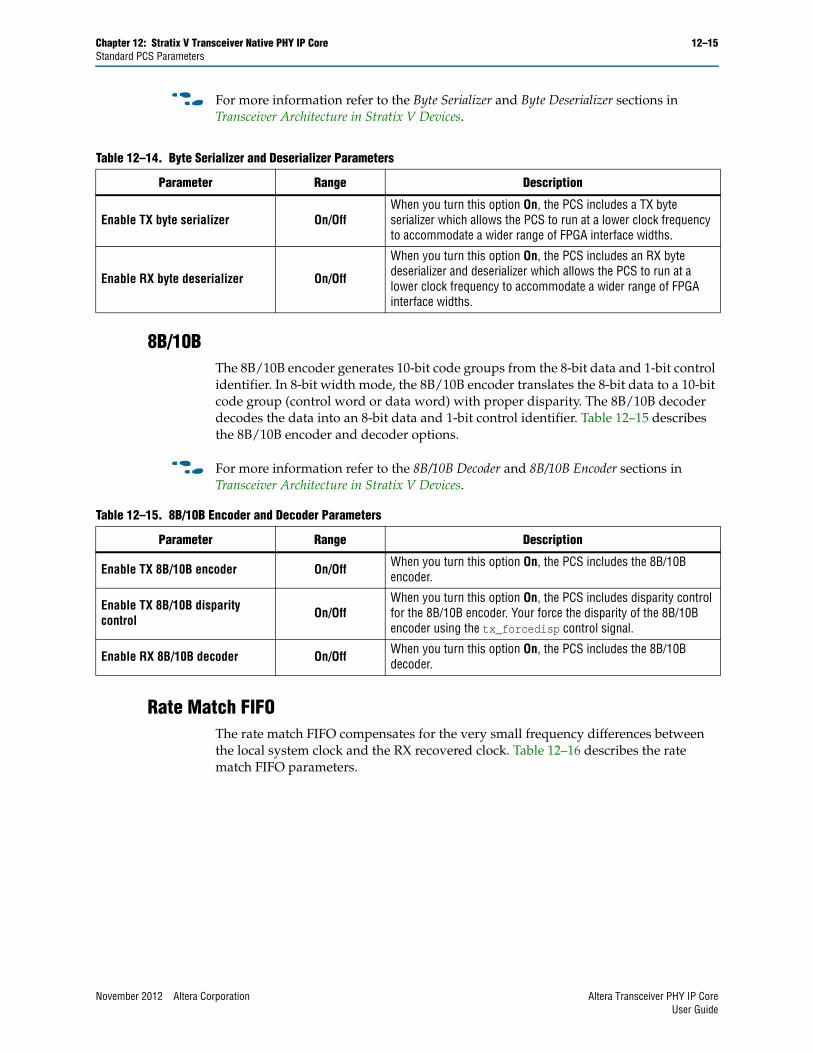
Chapter 12: Stratix V Transceiver Native PHY IP Core 12–15Standard PCS Parameters
f For more information refer to the Byte Serializer and Byte Deserializer sections in Transceiver Architecture in Stratix V Devices.
8B/10BThe 8B/10B encoder generates 10-bit code groups from the 8-bit data and 1-bit control identifier. In 8-bit width mode, the 8B/10B encoder translates the 8-bit data to a 10-bit code group (control word or data word) with proper disparity. The 8B/10B decoder decodes the data into an 8-bit data and 1-bit control identifier. Table 12–15 describes the 8B/10B encoder and decoder options.
f For more information refer to the 8B/10B Decoder and 8B/10B Encoder sections in Transceiver Architecture in Stratix V Devices.
Rate Match FIFOThe rate match FIFO compensates for the very small frequency differences between the local system clock and the RX recovered clock. Table 12–16 describes the rate match FIFO parameters.
Table 12–14. Byte Serializer and Deserializer Parameters
Parameter Range Description
Enable TX byte serializer On/OffWhen you turn this option On, the PCS includes a TX byte serializer which allows the PCS to run at a lower clock frequency to accommodate a wider range of FPGA interface widths.
Enable RX byte deserializer On/Off
When you turn this option On, the PCS includes an RX byte deserializer and deserializer which allows the PCS to run at a lower clock frequency to accommodate a wider range of FPGA interface widths.
Table 12–15. 8B/10B Encoder and Decoder Parameters
Parameter Range Description
Enable TX 8B/10B encoder On/Off When you turn this option On, the PCS includes the 8B/10B encoder.
Enable TX 8B/10B disparity control On/Off
When you turn this option On, the PCS includes disparity control for the 8B/10B encoder. Your force the disparity of the 8B/10B encoder using the tx_forcedisp control signal.
Enable RX 8B/10B decoder On/Off When you turn this option On, the PCS includes the 8B/10B decoder.
November 2012 Altera Corporation Altera Transceiver PHY IP CoreUser Guide
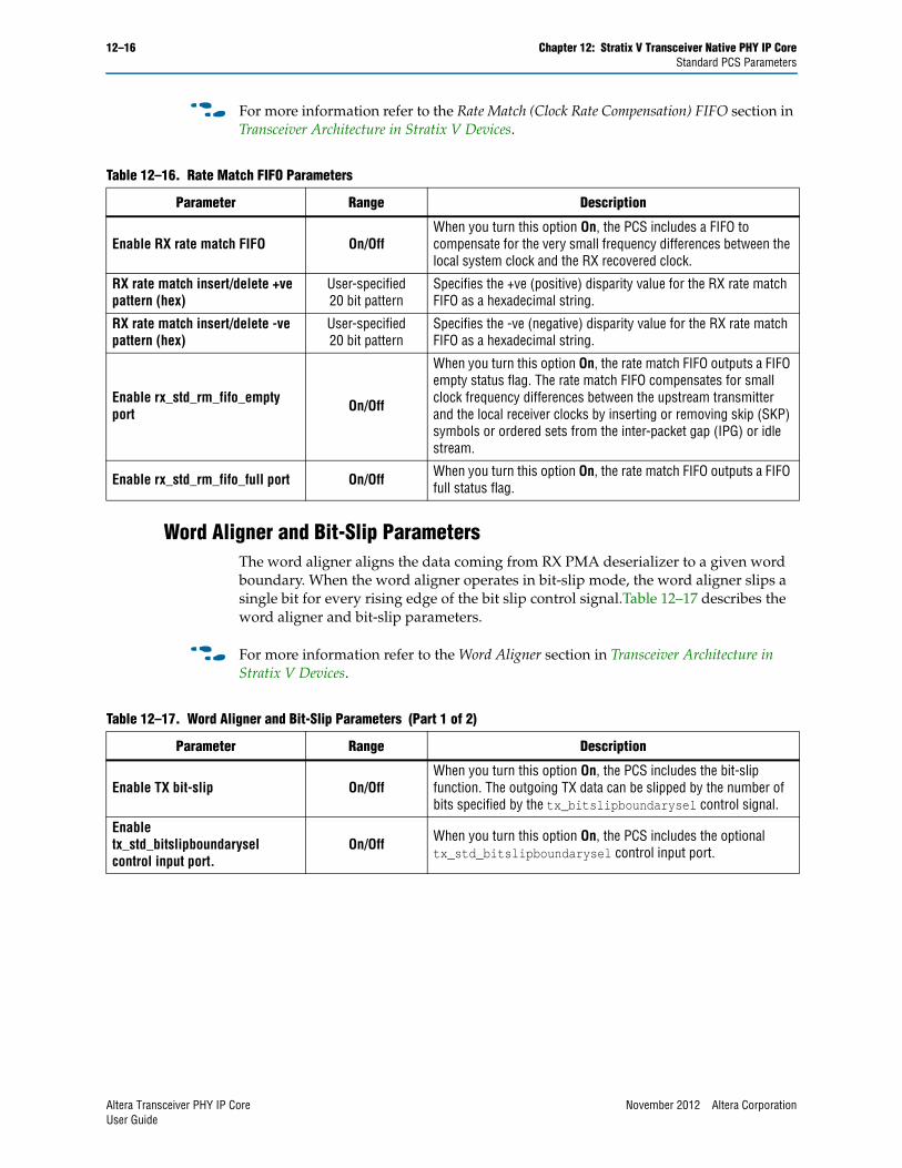
12–16 Chapter 12: Stratix V Transceiver Native PHY IP CoreStandard PCS Parameters
f For more information refer to the Rate Match (Clock Rate Compensation) FIFO section in Transceiver Architecture in Stratix V Devices.
Word Aligner and Bit-Slip ParametersThe word aligner aligns the data coming from RX PMA deserializer to a given word boundary. When the word aligner operates in bit-slip mode, the word aligner slips a single bit for every rising edge of the bit slip control signal.Table 12–17 describes the word aligner and bit-slip parameters.
f For more information refer to the Word Aligner section in Transceiver Architecture in Stratix V Devices.
Table 12–16. Rate Match FIFO Parameters
Parameter Range Description
Enable RX rate match FIFO On/OffWhen you turn this option On, the PCS includes a FIFO to compensate for the very small frequency differences between the local system clock and the RX recovered clock.
RX rate match insert/delete +ve pattern (hex)
User-specified 20 bit pattern
Specifies the +ve (positive) disparity value for the RX rate match FIFO as a hexadecimal string.
RX rate match insert/delete -ve pattern (hex)
User-specified 20 bit pattern
Specifies the -ve (negative) disparity value for the RX rate match FIFO as a hexadecimal string.
Enable rx_std_rm_fifo_empty port On/Off
When you turn this option On, the rate match FIFO outputs a FIFO empty status flag. The rate match FIFO compensates for small clock frequency differences between the upstream transmitter and the local receiver clocks by inserting or removing skip (SKP) symbols or ordered sets from the inter-packet gap (IPG) or idle stream.
Enable rx_std_rm_fifo_full port On/Off When you turn this option On, the rate match FIFO outputs a FIFO full status flag.
Table 12–17. Word Aligner and Bit-Slip Parameters (Part 1 of 2)
Parameter Range Description
Enable TX bit-slip On/OffWhen you turn this option On, the PCS includes the bit-slip function. The outgoing TX data can be slipped by the number of bits specified by the tx_bitslipboundarysel control signal.
Enable tx_std_bitslipboundarysel control input port.
On/Off When you turn this option On, the PCS includes the optional tx_std_bitslipboundarysel control input port.
Altera Transceiver PHY IP Core November 2012 Altera CorporationUser Guide
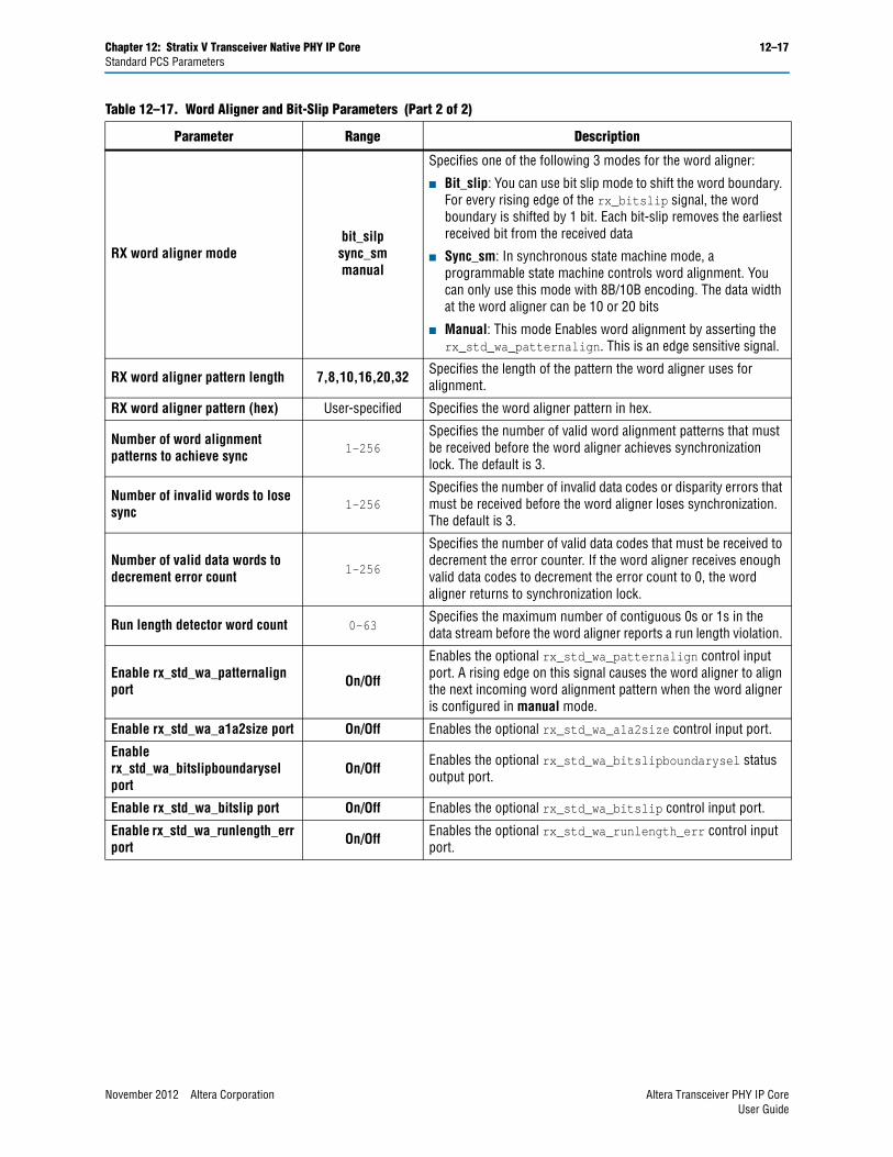
Chapter 12: Stratix V Transceiver Native PHY IP Core 12–17Standard PCS Parameters
RX word aligner modebit_silpsync_smmanual
Specifies one of the following 3 modes for the word aligner:
■ Bit_slip: You can use bit slip mode to shift the word boundary. For every rising edge of the rx_bitslip signal, the word boundary is shifted by 1 bit. Each bit-slip removes the earliest received bit from the received data
■ Sync_sm: In synchronous state machine mode, a programmable state machine controls word alignment. You can only use this mode with 8B/10B encoding. The data width at the word aligner can be 10 or 20 bits
■ Manual: This mode Enables word alignment by asserting the rx_std_wa_patternalign. This is an edge sensitive signal.
RX word aligner pattern length 7,8,10,16,20,32 Specifies the length of the pattern the word aligner uses for alignment.
RX word aligner pattern (hex) User-specified Specifies the word aligner pattern in hex.
Number of word alignment patterns to achieve sync 1–256
Specifies the number of valid word alignment patterns that must be received before the word aligner achieves synchronization lock. The default is 3.
Number of invalid words to lose sync 1–256
Specifies the number of invalid data codes or disparity errors that must be received before the word aligner loses synchronization. The default is 3.
Number of valid data words to decrement error count 1–256
Specifies the number of valid data codes that must be received to decrement the error counter. If the word aligner receives enough valid data codes to decrement the error count to 0, the word aligner returns to synchronization lock.
Run length detector word count 0–63Specifies the maximum number of contiguous 0s or 1s in the data stream before the word aligner reports a run length violation.
Enable rx_std_wa_patternalign port On/Off
Enables the optional rx_std_wa_patternalign control input port. A rising edge on this signal causes the word aligner to align the next incoming word alignment pattern when the word aligner is configured in manual mode.
Enable rx_std_wa_a1a2size port On/Off Enables the optional rx_std_wa_a1a2size control input port.
Enable rx_std_wa_bitslipboundarysel port
On/Off Enables the optional rx_std_wa_bitslipboundarysel status output port.
Enable rx_std_wa_bitslip port On/Off Enables the optional rx_std_wa_bitslip control input port.
Enable rx_std_wa_runlength_err port On/Off Enables the optional rx_std_wa_runlength_err control input
port.
Table 12–17. Word Aligner and Bit-Slip Parameters (Part 2 of 2)
Parameter Range Description
November 2012 Altera Corporation Altera Transceiver PHY IP CoreUser Guide
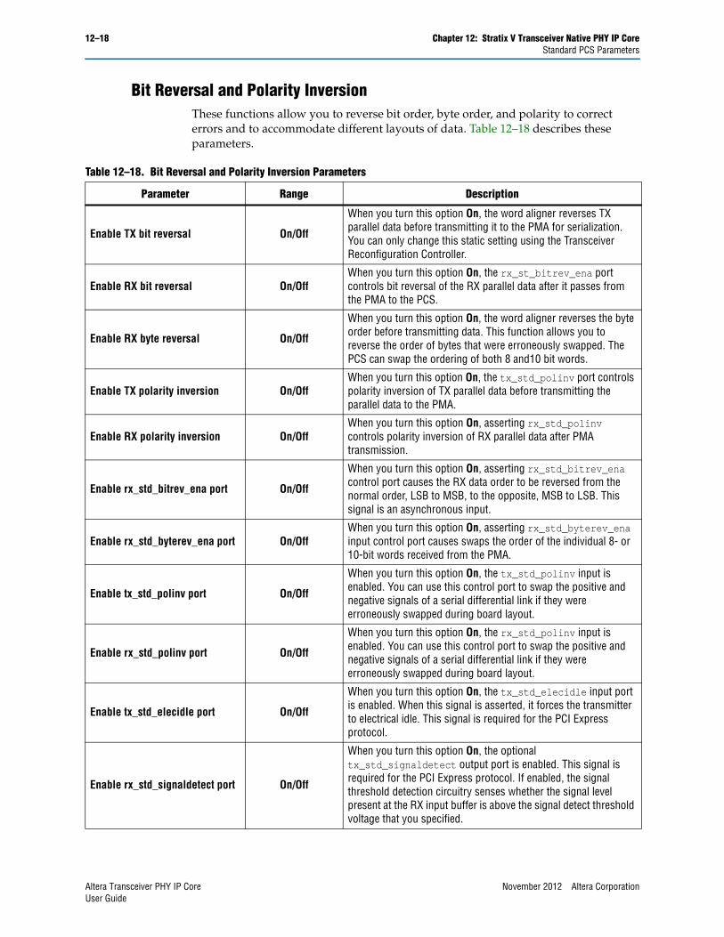
12–18 Chapter 12: Stratix V Transceiver Native PHY IP CoreStandard PCS Parameters
Bit Reversal and Polarity InversionThese functions allow you to reverse bit order, byte order, and polarity to correct errors and to accommodate different layouts of data. Table 12–18 describes these parameters.
Table 12–18. Bit Reversal and Polarity Inversion Parameters
Parameter Range Description
Enable TX bit reversal On/Off
When you turn this option On, the word aligner reverses TX parallel data before transmitting it to the PMA for serialization. You can only change this static setting using the Transceiver Reconfiguration Controller.
Enable RX bit reversal On/OffWhen you turn this option On, the rx_st_bitrev_ena port controls bit reversal of the RX parallel data after it passes from the PMA to the PCS.
Enable RX byte reversal On/Off
When you turn this option On, the word aligner reverses the byte order before transmitting data. This function allows you to reverse the order of bytes that were erroneously swapped. The PCS can swap the ordering of both 8 and10 bit words.
Enable TX polarity inversion On/OffWhen you turn this option On, the tx_std_polinv port controls polarity inversion of TX parallel data before transmitting the parallel data to the PMA.
Enable RX polarity inversion On/OffWhen you turn this option On, asserting rx_std_polinv controls polarity inversion of RX parallel data after PMA transmission.
Enable rx_std_bitrev_ena port On/Off
When you turn this option On, asserting rx_std_bitrev_ena control port causes the RX data order to be reversed from the normal order, LSB to MSB, to the opposite, MSB to LSB. This signal is an asynchronous input.
Enable rx_std_byterev_ena port On/OffWhen you turn this option On, asserting rx_std_byterev_ena input control port causes swaps the order of the individual 8- or 10-bit words received from the PMA.
Enable tx_std_polinv port On/Off
When you turn this option On, the tx_std_polinv input is enabled. You can use this control port to swap the positive and negative signals of a serial differential link if they were erroneously swapped during board layout.
Enable rx_std_polinv port On/Off
When you turn this option On, the rx_std_polinv input is enabled. You can use this control port to swap the positive and negative signals of a serial differential link if they were erroneously swapped during board layout.
Enable tx_std_elecidle port On/Off
When you turn this option On, the tx_std_elecidle input port is enabled. When this signal is asserted, it forces the transmitter to electrical idle. This signal is required for the PCI Express protocol.
Enable rx_std_signaldetect port On/Off
When you turn this option On, the optional tx_std_signaldetect output port is enabled. This signal is required for the PCI Express protocol. If enabled, the signal threshold detection circuitry senses whether the signal level present at the RX input buffer is above the signal detect threshold voltage that you specified.
Altera Transceiver PHY IP Core November 2012 Altera CorporationUser Guide
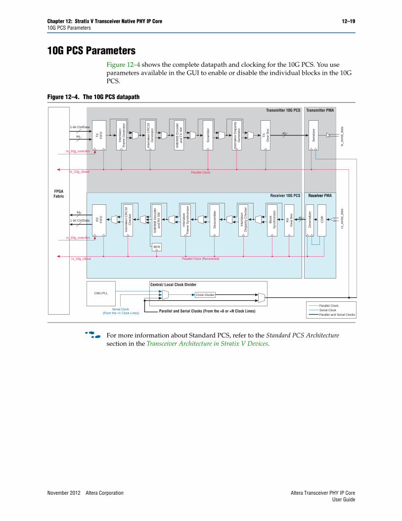
Chapter 12: Stratix V Transceiver Native PHY IP Core 12–1910G PCS Parameters
10G PCS ParametersFigure 12–4 shows the complete datapath and clocking for the 10G PCS. You use parameters available in the GUI to enable or disable the individual blocks in the 10G PCS.
f For more information about Standard PCS, refer to the Standard PCS Architecture section in the Transceiver Architecture in Stratix V Devices.
Figure 12–4. The 10G PCS datapath
FPGAFabric
Transmitter 10G PCS
Receiver 10G PCS
Transmitter PMA
Receiver Receiver PMA
TX
FIF
OR
XF
IFO
Inte
rlake
nFr
ame
Gen
erat
or
Inte
rlake
n C
RC
32G
ener
ator
Inte
rlake
n C
RC
32C
heck
er
64B
/66B
Enc
oder
and
TX
SM
64B
/66B
Dec
oder
and
RX
SM
Scr
ambl
er
Des
cram
bler
Inte
rlake
nD
ispa
rity
Che
cker
Blo
ckS
ynch
roni
zer
Inte
rlake
nFr
ame
Syn
chro
nize
r
Inte
rlake
n D
ispa
rity
Gen
erat
or
TX
Gea
r B
ox
RX
Gea
r B
ox
64
64
Parallel Clock (Recovered)
Parallel Clock
40
Ser
ializ
erD
eser
ializ
er
CD
R
tx_s
eria
l_da
tarx
_ser
ial_
data
1-bit Ctrl/Data
1 bit Ctrl/Data40
Clock Divider
BER
Parallel and Serial Clocks (From the ×6 or ×N Clock Lines)Serial Clock (From the ×1 Clock Lines)
Central/ Local Clock Divider
Parallel ClockSerial ClockParallel and Serial Clocks
CMU PLL
tx_10g_coreclkin
rx_10g_coreclkin
tx_10g_clkout
rx_10g_clkout
November 2012 Altera Corporation Altera Transceiver PHY IP CoreUser Guide
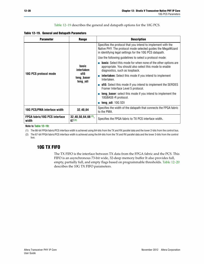
12–20 Chapter 12: Stratix V Transceiver Native PHY IP Core10G PCS Parameters
Table 12–19 describes the general and datapath options for the 10G PCS.
10G TX FIFOThe TX FIFO is the interface between TX data from the FPGA fabric and the PCS. This FIFO is an asynchronous 73-bit wide, 32-deep memory buffer It also provides full, empty, partially full, and empty flags based on programmable thresholds. Table 12–20 describes the 10G TX FIFO parameters.
Table 12–19. General and Datapath Parameters
Parameter Range Description
10G PCS protocol mode
basicinterlaken
sfi5teng_baser
teng_sdi
Specifies the protocol that you intend to implement with the Native PHY. The protocol mode selected guides the MegaWizard in identifying legal settings for the 10G PCS datapath.
Use the following guidelines to select a protocol mode:
■ basic: Select this mode for when none of the other options are appropriate. You should also select this mode to enable diagnostics, such as loopback.
■ interlaken: Select this mode if you intend to implement Interlaken.
■ sfi5: Select this mode if you intend to implement the SERDES Framer Interface Level 5 protocol.
■ teng_baser: select this mode if you intend to implement the 10GBASE-R protocol.
■ teng_sdi: 10G SDI
10G PCS/PMA interface width 32.40,64 Specifies the width of the datapath that connects the FPGA fabric to the PMA.
FPGA fabric/10G PCS interface width
32,40,50,64,66 (1),67 (2) Specifies the FPGA fabric to TX PCS interface width.
Note to Table 12–19:
(1) The 66-bit FPGA fabric/PCS interface width is achieved using 64-bits from the TX and RX parallel data and the lower 2-bits from the control bus.(2) The 67-bit FPGA fabric/PCS interface width is achieved using the 64-bits from the TX and RX parallel data and the lower 3-bits from the control
bus.
Altera Transceiver PHY IP Core November 2012 Altera CorporationUser Guide
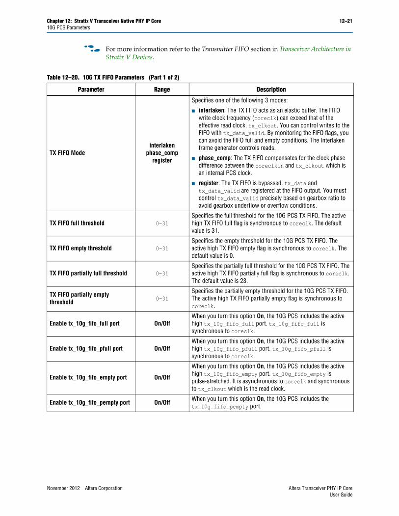
Chapter 12: Stratix V Transceiver Native PHY IP Core 12–2110G PCS Parameters
f For more information refer to the Transmitter FIFO section in Transceiver Architecture in Stratix V Devices.
Table 12–20. 10G TX FIFO Parameters (Part 1 of 2)
Parameter Range Description
TX FIFO Modeinterlaken
phase_compregister
Specifies one of the following 3 modes:
■ interlaken: The TX FIFO acts as an elastic buffer. The FIFO write clock frequency (coreclk) can exceed that of the effective read clock, tx_clkout. You can control writes to the FIFO with tx_data_valid. By monitoring the FIFO flags, you can avoid the FIFO full and empty conditions. The Interlaken frame generator controls reads.
■ phase_comp: The TX FIFO compensates for the clock phase difference between the coreclkin and tx_clkout which is an internal PCS clock.
■ register: The TX FIFO is bypassed. tx_data and tx_data_valid are registered at the FIFO output. You must control tx_data_valid precisely based on gearbox ratio to avoid gearbox underflow or overflow conditions.
TX FIFO full threshold 0–31Specifies the full threshold for the 10G PCS TX FIFO. The active high TX FIFO full flag is synchronous to coreclk. The default value is 31.
TX FIFO empty threshold 0–31Specifies the empty threshold for the 10G PCS TX FIFO. The active high TX FIFO empty flag is synchronous to coreclk. The default value is 0.
TX FIFO partially full threshold 0–31Specifies the partially full threshold for the 10G PCS TX FIFO. The active high TX FIFO partially full flag is synchronous to coreclk. The default value is 23.
TX FIFO partially empty threshold 0–31
Specifies the partially empty threshold for the 10G PCS TX FIFO. The active high TX FIFO partially empty flag is synchronous to coreclk.
Enable tx_10g_fifo_full port On/OffWhen you turn this option On, the 10G PCS includes the active high tx_10g_fifo_full port. tx_10g_fifo_full is synchronous to coreclk.
Enable tx_10g_fifo_pfull port On/OffWhen you turn this option On, the 10G PCS includes the active high tx_10g_fifo_pfull port. tx_10g_fifo_pfull is synchronous to coreclk.
Enable tx_10g_fifo_empty port On/Off
When you turn this option On, the 10G PCS includes the active high tx_10g_fifo_empty port. tx_10g_fifo_empty is pulse-stretched. It is asynchronous to coreclk and synchronous to tx_clkout which is the read clock.
Enable tx_10g_fifo_pempty port On/Off When you turn this option On, the 10G PCS includes the tx_10g_fifo_pempty port.
November 2012 Altera Corporation Altera Transceiver PHY IP CoreUser Guide
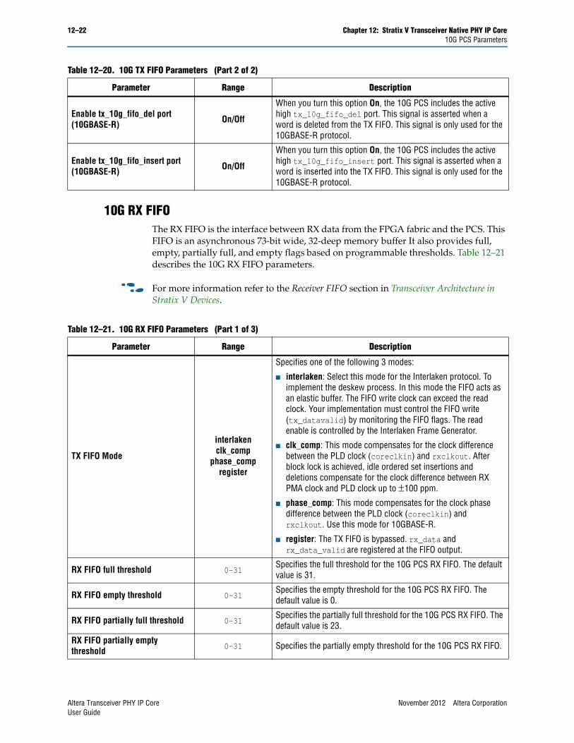
12–22 Chapter 12: Stratix V Transceiver Native PHY IP Core10G PCS Parameters
10G RX FIFOThe RX FIFO is the interface between RX data from the FPGA fabric and the PCS. This FIFO is an asynchronous 73-bit wide, 32-deep memory buffer It also provides full, empty, partially full, and empty flags based on programmable thresholds. Table 12–21 describes the 10G RX FIFO parameters.
f For more information refer to the Receiver FIFO section in Transceiver Architecture in Stratix V Devices.
Enable tx_10g_fifo_del port (10GBASE-R) On/Off
When you turn this option On, the 10G PCS includes the active high tx_10g_fifo_del port. This signal is asserted when a word is deleted from the TX FIFO. This signal is only used for the 10GBASE-R protocol.
Enable tx_10g_fifo_insert port (10GBASE-R) On/Off
When you turn this option On, the 10G PCS includes the active high tx_10g_fifo_insert port. This signal is asserted when a word is inserted into the TX FIFO. This signal is only used for the 10GBASE-R protocol.
Table 12–20. 10G TX FIFO Parameters (Part 2 of 2)
Parameter Range Description
Table 12–21. 10G RX FIFO Parameters (Part 1 of 3)
Parameter Range Description
TX FIFO Mode
interlakenclk_comp
phase_compregister
Specifies one of the following 3 modes:
■ interlaken: Select this mode for the Interlaken protocol. To implement the deskew process. In this mode the FIFO acts as an elastic buffer. The FIFO write clock can exceed the read clock. Your implementation must control the FIFO write (tx_datavalid) by monitoring the FIFO flags. The read enable is controlled by the Interlaken Frame Generator.
■ clk_comp: This mode compensates for the clock difference between the PLD clock (coreclkin) and rxclkout. After block lock is achieved, idle ordered set insertions and deletions compensate for the clock difference between RX PMA clock and PLD clock up to 100 ppm.
■ phase_comp: This mode compensates for the clock phase difference between the PLD clock (coreclkin) and rxclkout. Use this mode for 10GBASE-R.
■ register: The TX FIFO is bypassed. rx_data and rx_data_valid are registered at the FIFO output.
RX FIFO full threshold 0–31Specifies the full threshold for the 10G PCS RX FIFO. The default value is 31.
RX FIFO empty threshold 0–31Specifies the empty threshold for the 10G PCS RX FIFO. The default value is 0.
RX FIFO partially full threshold 0–31Specifies the partially full threshold for the 10G PCS RX FIFO. The default value is 23.
RX FIFO partially empty threshold 0–31 Specifies the partially empty threshold for the 10G PCS RX FIFO.
Altera Transceiver PHY IP Core November 2012 Altera CorporationUser Guide
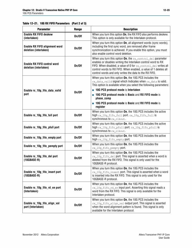
Chapter 12: Stratix V Transceiver Native PHY IP Core 12–2310G PCS Parameters
Enable RX FIFO deskew (interlaken) On/Off When you turn this option On, the RX FIFO also performs deskew.
This option is only available for the Interlaken protocol.
Enable RX FIFO alignment word deletion (interlaken) On/Off
When you turn this option On, all alignment words (sync words), including the first sync word, are removed after frame synchronization is achieved. If you enable this option, you must also enable control word deletion.
Enable RX FIFO control word deletion (interlaken) On/Off
When you turn this option On, the rx_control_del parameter enables or disables writing the Interlaken control word to RX FIFO. When disabled, a value of 0 for rx_control_del writes all control words to RX FIFO. When enabled, a value of 1 deletes all control words and only writes the data to the RX FIFO.
Enable rx_10g_fifo_data_valid port On/Off
When you turn this option On, the 10G PCS includes the rx_data_valid signal which Indicates when rx_data is valid. This option is available when you select the following parameters:
■ 10G PCS protocol mode is Interlaken
■ 10G PCS protocol mode is Basic and RX FIFO mode is phase_comp
■ 10G PCS protocol mode is Basic and RX FIFO mode is register
Enable rx_10g_fifo_full port On/OffWhen you turn this option On, the 10G PCS includes the active high rx_10g_fifo_full port. rx_10g_fifo_full is synchronous to rx_clkout.
Enable rx_10g_fifo_pfull port On/OffWhen you turn this option On, the 10G PCS includes the active high rx_10g_fifo_pfull port. rx_10g_fifo_pfull is synchronous to rx_clkout.
Enable rx_10g_fifo_empty port On/Off When you turn this option On, the 10G PCS includes the active high rx_10g_fifo_empty port.
Enable rx_10g_fifo_pempty port On/Off When you turn this option On, the 10G PCS includes the rx_10g_fifo_pempty port.
Enable rx_10g_fifo_del port (10GBASE-R) On/Off
When you turn this option On, the 10G PCS includes the rx_10g_fifo_del port. This signal is asserted when a word is deleted from the RX FIFO. This signal is only used for the 10GBASE-R protocol.
Enable rx_10g_fifo_insert port (10GBASE-R) On/Off
When you turn this option On, the 10G PCS includes the rx_10g_fifo_insert port. This signal is asserted when a word is inserted into the RX FIFO. This signal is only used for the 10GBASE-R protocol.
Enable rx_10g_fifo_rd_en port (Interlaken) On/Off
When you turn this option On, the 10G PCS includes the rx_10g_fifo_rd_en input port. Asserting this signal reads a word from the RX FIFO. This signal is only available for the Interlaken protocol.
Enable rx_10g_fifo_align_val port (Interlaken) On/Off
When you turn this option On, the 10G PCS includes the rx_10g_fifo_align_val output port. This signal is asserted when the word alignment pattern is found. This signal is only available for the Interlaken protocol.
Table 12–21. 10G RX FIFO Parameters (Part 2 of 3)
Parameter Range Description
November 2012 Altera Corporation Altera Transceiver PHY IP CoreUser Guide
12–24 Chapter 12: Stratix V Transceiver Native PHY IP Core10G PCS Parameters
Interlaken Frame Generator TX Frame generator generates the metaframe. It encapsulates the payload from MAC with the framing layer control words, including sync, scrambler, skip and diagnostic words. Table 12–22 describes the Interlaken frame generator parameters.
f For more information refer to the Frame Generator section in Transceiver Architecture in Stratix V Devices.
Enable rx_10g_fifo_align_clr port (Interlaken) On/Off
When you turn this option On, the 10G PCS includes the rx_10g_fifo_align_clr input port. When this signal is asserted, the FIFO resets and begins searching for a new alignment pattern. This signal is only available for the Interlaken protocol.
Enable rx_10g_fifo_align_en port (Interlaken) On/Off
When you turn this option On, the 10G PCS includes the rx_10g_fifo_align_en input port. This signal is used for FIFO deskew for Interlaken. When asserted, the corresponding channel is enabled for alignment. This signal is only available for the Interlaken protocol.
Table 12–21. 10G RX FIFO Parameters (Part 3 of 3)
Parameter Range Description
Table 12–22. Interlaken Frame Generator Parameters (Part 1 of 2)
Parameter Range Description
teng_tx_framgen_enable On/Off When you turn this option On, the frame generator block of the 10G PCS is enabled.
teng_tx_framgen_user_length 0-8192 Specifies the metaframe length.
teng_tx_framgen_burst_enable On/Off When you turn this option On, the frame generator burst functionality is enabled.
Enable tx_10g_frame port On/Off
When you turn this option On, the 10G PCS includes the tx_10g_frame output port. When asserted, tx_10g_frame indicates the beginning of a new metaframe inside the frame generator.
Altera Transceiver PHY IP Core November 2012 Altera CorporationUser Guide
Chapter 12: Stratix V Transceiver Native PHY IP Core 12–2510G PCS Parameters
Interlaken Frame SynchronizerThe Interlaken frame synchronizer block achieves lock by looking for four synchronization words in consecutive metaframes. After synchronization, the frame synchronizer monitors the scrambler word in the metaframe and deasserts the lock signal after three consecutive mismatches and starts the synchronization process again. Lock status is available to the FPGA fabric. Table 12–23 describes the Interlaken frame synchronizer parameters.
f For more information refer to the Frame Synchronizer section in Transceiver Architecture in Stratix V Devices.
Enable tx_10g_frame_diag_status port On/Off
When you turn this option On, the 10G PCS includes the tx_10g_frame_diag_status 2-bit input port.
This port contains the lane Status Message from the framing layer Diagnostic Word, bits[33:32]. This message is inserted into the next Diagnostic Word generated by the frame generation block. The message must be held static for 5 cycles before and 5 cycles after the tx_frame pulse.
Enable tx_10g_frame_burst_en port On/Off
When you turn this option On, the 10G PCS includes the tx_10g_frame_burst_en input port.
This port controls frame generator data reads from the TX FIFO. The value of this signal is latched once at the beginning of each Metaframe. It controls whether data is read from the TX FIFO or SKIP Words are inserted for the current Metaframe. It must be held static for 5 cycles before and 5 cycles after the tx_frame pulse.
When tx_10g_frame_burst_en is 0, the frame generator does not read data from the TX FIFO for current Metaframe. It insert SKIPs. When tx_10g_frame_burst_en is 1, the frame generator reads data from the TX FIFO for current Metaframe.
Table 12–22. Interlaken Frame Generator Parameters (Part 2 of 2)
Parameter Range Description
Table 12–23. Interlaken Frame Synchronizer Parameters (Part 1 of 2)
Parameter Range Description
teng_tx_framsync_enable On/Off When you turn this option On, the 10G PCS frame generator is enabled.
Enable rx_10g_frame port On/OffWhen you turn this option On, the 10G PCS includes the rx_10g_frame output port. This signal is asserted to indicate the beginning of a new metaframe inside.
Enable rx_10g_frame_lock_port On/Off
When you turn this option On, the 10G PCS includes the rx_10g_frame_lock output port. This signal is asserted to indicate that the frame synchronization state machine has achieved frame lock.
Enable rx_10g_frame_mfrm_err port On/Off
When you turn this option On, the 10G PCS includes the rx_10g_frame_mfrm_err output port. This signal is asserted to indicate an metaframe error.
November 2012 Altera Corporation Altera Transceiver PHY IP CoreUser Guide
12–26 Chapter 12: Stratix V Transceiver Native PHY IP Core10G PCS Parameters
Enable rx_10g_frame_sync_err port On/Off
When you turn this option On, the 10G PCS includes the rx_10g_frame_sync_err output port. This signal is asserted to indicate synchronization control word errors. This signal remains asserted during the loss of block_lock and does not update until block_lock is recovered.
Enable rx_10g_frame_skip_ins port On/Off
When you turn this option On, the 10G PCS includes the rx_10g_frame_skip_ins output port. This signal is asserted to indicate a SKIP word was received by the frame sync in a non-SKIP word location within the metaframe.
Enable rx_10g_frame_pyld_ins port On/Off
When you turn this option On, the 10G PCS includes the rx_10g_frame_pyld_ins output port. This signal is asserted to indicate a SKIP word was not received by the frame sync in a SKIP word location within the metaframe.
Enable rx_10g_frame_skip_err port On/Off
When you turn this option On, the 10G PCS includes the rx_10g_frame_skip_err output port. This signal is asserted to indicate the frame synchronization has received an erroneous word in a Skip control word location within the Metaframe. This signal remains asserted during the loss of block_lock and does update until block_lock is recovered.
Enable rx_10g_frame_diag_err port On/Off
When you turn this option On, the 10G PCS includes the rx_10g_frame_diag_err output port. This signal is asserted to indicate a diagnostic control word error. This signal remains asserted during the loss of block_lock and does update until block_lock is recovered.
Enable rx_10g_frame_diag_status port On/Off
When you turn this option On, the 10G PCS includes the rx_10g_frame_diag_status 2-bit output port per channel. This port contains the lane Status Message from the framing layer Diagnostic Word, bits[33:32]. This message is inserted into the next Diagnostic Word generated by the frame generation block.
Table 12–23. Interlaken Frame Synchronizer Parameters (Part 2 of 2)
Parameter Range Description
Altera Transceiver PHY IP Core November 2012 Altera CorporationUser Guide
Chapter 12: Stratix V Transceiver Native PHY IP Core 12–2710G PCS Parameters
Interlaken CRC32 Generator and CheckerCRC-32 provides a diagnostic tool on a per-lane basis. You can use CRC-32 to trace interface errors back to an individual lane. The CRC-32 calculation covers the whole metaframe including the Diagnostic Word itself. This CRC code value is stored in the CRC32 field of the Diagnostic Word. Table 12–24 describes the CRC-32 parameters.
f For more information refer to the CRC-32 Generator section in Transceiver Architecture in Stratix V Devices
10GBASE-R BER CheckerThe BER monitor block conforms to the 10GBASE-R protocol specification as described in IEEE 802.3-2008 Clause-49. After block lock is achieved, the BER monitor starts to count the number of invalid synchronization headers within a 125-s period. If more than 16 invalid synchronization headers are observed in a 125-s period, the BER monitor provides the status signal to the FPGA fabric, indicating a high bit error. Table 12–25 describes the 10GBASE-R BER checker parameters.
f For more information refer to the Bit-Error Rate (BER) section in Transceiver Architecture in Stratix V Devices.
Table 12–24. Interlaken CRC32 Generator and Checker Parameters
Parameter Range Description
Enable Interlaken TX CRC32 Generator On/Off When you turn this option On, the TX 10G PCS datapath includes
the CRC32 function.
Enable Interlaken RX CRC32 Generator On/Off When you turn this option On, the RX 10G PCS datapath includes
the CRC32 function.
Enable rx_10g_crc32_err port On/OffWhen you turn this option On, the 10G PCS includes the rx_10g_crc32_err port. This signal is asserted to indicate that the CRC checker has found an error in the current metaframe.
Table 12–25. 10GBASE-R BER Checker Parameters
Parameter Range Description
Enable rx_10g_highber port (10GBASE-R) On/Off
When you turn this option On, the TX 10G PCS datapath includes the rx_10g_highber output port. This signal is asserted to indicate a BER of >104. A count of 16 errors in 125-s period indicates a BER > 104. This signal is only available for the 10GBASE-R protocol.
Enable rx_10g_highber_clr_cnt port (10GBASE-R) On/Off
When you turn this option On, the TX 10G PCS datapath includes the rx_10g_highber_clr_cnt input port. When asserted, the BER counter resets to 0. This signal is only available for the 10GBASE-R protocol.
Enable rx_10g_clr_errblk_count port (10GBASE-R) On/Off
When you turn this option On, the 10G PCS includes the rx_10g_clr_errblk_count input port. When asserted, error block counter that counts the number of RX errors resets to 0. This signal is only available for the 10GBASE-R protocol.
November 2012 Altera Corporation Altera Transceiver PHY IP CoreUser Guide
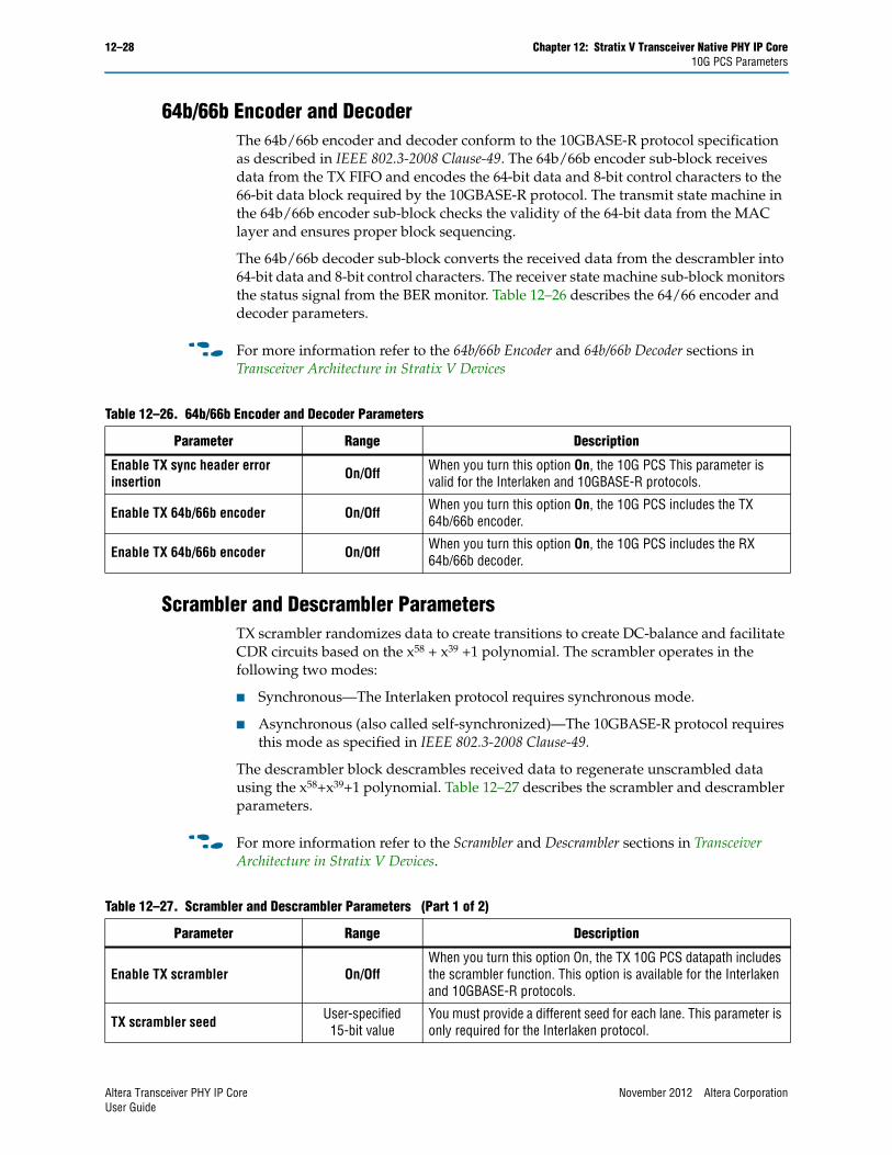
12–28 Chapter 12: Stratix V Transceiver Native PHY IP Core10G PCS Parameters
64b/66b Encoder and DecoderThe 64b/66b encoder and decoder conform to the 10GBASE-R protocol specification as described in IEEE 802.3-2008 Clause-49. The 64b/66b encoder sub-block receives data from the TX FIFO and encodes the 64-bit data and 8-bit control characters to the 66-bit data block required by the 10GBASE-R protocol. The transmit state machine in the 64b/66b encoder sub-block checks the validity of the 64-bit data from the MAC layer and ensures proper block sequencing.
The 64b/66b decoder sub-block converts the received data from the descrambler into 64-bit data and 8-bit control characters. The receiver state machine sub-block monitors the status signal from the BER monitor. Table 12–26 describes the 64/66 encoder and decoder parameters.
f For more information refer to the 64b/66b Encoder and 64b/66b Decoder sections in Transceiver Architecture in Stratix V Devices
Scrambler and Descrambler ParametersTX scrambler randomizes data to create transitions to create DC-balance and facilitate CDR circuits based on the x58 + x39 +1 polynomial. The scrambler operates in the following two modes:
■ Synchronous—The Interlaken protocol requires synchronous mode.
■ Asynchronous (also called self-synchronized)—The 10GBASE-R protocol requires this mode as specified in IEEE 802.3-2008 Clause-49.
The descrambler block descrambles received data to regenerate unscrambled data using the x58+x39+1 polynomial. Table 12–27 describes the scrambler and descrambler parameters.
f For more information refer to the Scrambler and Descrambler sections in Transceiver Architecture in Stratix V Devices.
Table 12–26. 64b/66b Encoder and Decoder Parameters
Parameter Range Description
Enable TX sync header error insertion On/Off When you turn this option On, the 10G PCS This parameter is
valid for the Interlaken and 10GBASE-R protocols.
Enable TX 64b/66b encoder On/Off When you turn this option On, the 10G PCS includes the TX 64b/66b encoder.
Enable TX 64b/66b encoder On/Off When you turn this option On, the 10G PCS includes the RX 64b/66b decoder.
Table 12–27. Scrambler and Descrambler Parameters (Part 1 of 2)
Parameter Range Description
Enable TX scrambler On/OffWhen you turn this option On, the TX 10G PCS datapath includes the scrambler function. This option is available for the Interlaken and 10GBASE-R protocols.
TX scrambler seed User-specified15-bit value
You must provide a different seed for each lane. This parameter is only required for the Interlaken protocol.
Altera Transceiver PHY IP Core November 2012 Altera CorporationUser Guide
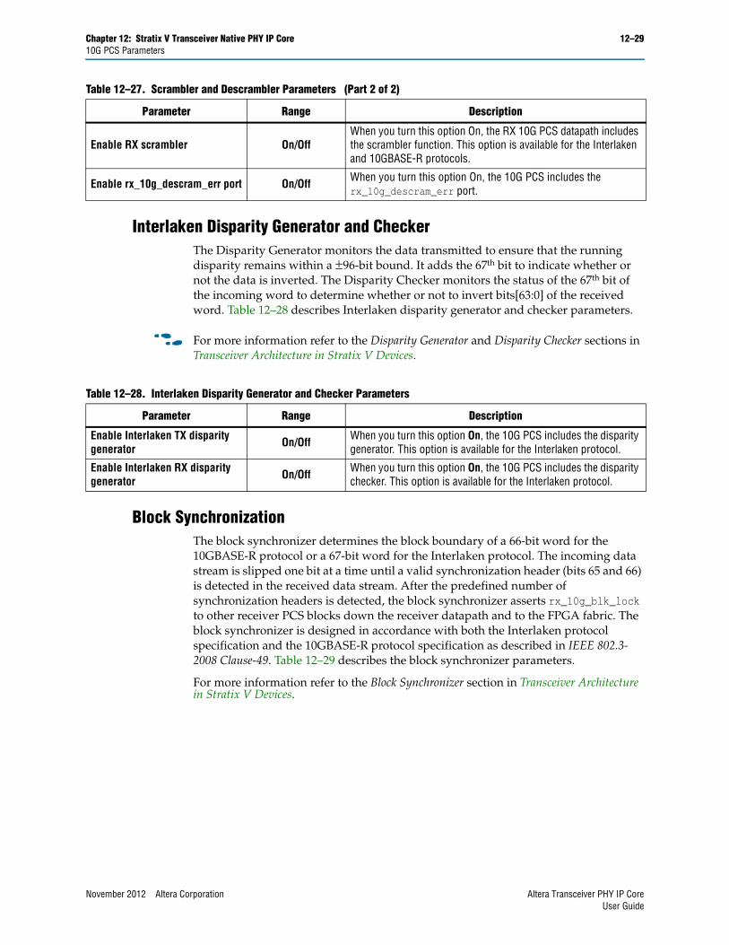
Chapter 12: Stratix V Transceiver Native PHY IP Core 12–2910G PCS Parameters
Interlaken Disparity Generator and CheckerThe Disparity Generator monitors the data transmitted to ensure that the running disparity remains within a 96-bit bound. It adds the 67th bit to indicate whether or not the data is inverted. The Disparity Checker monitors the status of the 67th bit of the incoming word to determine whether or not to invert bits[63:0] of the received word. Table 12–28 describes Interlaken disparity generator and checker parameters.
f For more information refer to the Disparity Generator and Disparity Checker sections in Transceiver Architecture in Stratix V Devices.
Block SynchronizationThe block synchronizer determines the block boundary of a 66-bit word for the 10GBASE-R protocol or a 67-bit word for the Interlaken protocol. The incoming data stream is slipped one bit at a time until a valid synchronization header (bits 65 and 66) is detected in the received data stream. After the predefined number of synchronization headers is detected, the block synchronizer asserts rx_10g_blk_lock to other receiver PCS blocks down the receiver datapath and to the FPGA fabric. The block synchronizer is designed in accordance with both the Interlaken protocol specification and the 10GBASE-R protocol specification as described in IEEE 802.3-2008 Clause-49. Table 12–29 describes the block synchronizer parameters.
For more information refer to the Block Synchronizer section in Transceiver Architecture in Stratix V Devices.
Enable RX scrambler On/OffWhen you turn this option On, the RX 10G PCS datapath includes the scrambler function. This option is available for the Interlaken and 10GBASE-R protocols.
Enable rx_10g_descram_err port On/Off When you turn this option On, the 10G PCS includes the rx_10g_descram_err port.
Table 12–27. Scrambler and Descrambler Parameters (Part 2 of 2)
Parameter Range Description
Table 12–28. Interlaken Disparity Generator and Checker Parameters
Parameter Range Description
Enable Interlaken TX disparity generator On/Off When you turn this option On, the 10G PCS includes the disparity
generator. This option is available for the Interlaken protocol.
Enable Interlaken RX disparity generator On/Off When you turn this option On, the 10G PCS includes the disparity
checker. This option is available for the Interlaken protocol.
November 2012 Altera Corporation Altera Transceiver PHY IP CoreUser Guide
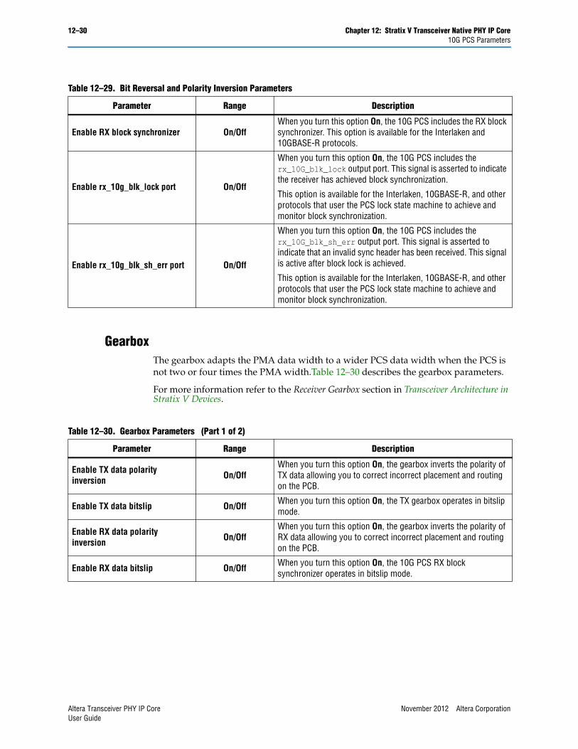
12–30 Chapter 12: Stratix V Transceiver Native PHY IP Core10G PCS Parameters
GearboxThe gearbox adapts the PMA data width to a wider PCS data width when the PCS is not two or four times the PMA width.Table 12–30 describes the gearbox parameters.
For more information refer to the Receiver Gearbox section in Transceiver Architecture in Stratix V Devices.
Table 12–29. Bit Reversal and Polarity Inversion Parameters
Parameter Range Description
Enable RX block synchronizer On/OffWhen you turn this option On, the 10G PCS includes the RX block synchronizer. This option is available for the Interlaken and 10GBASE-R protocols.
Enable rx_10g_blk_lock port On/Off
When you turn this option On, the 10G PCS includes the rx_10G_blk_lock output port. This signal is asserted to indicate the receiver has achieved block synchronization.
This option is available for the Interlaken, 10GBASE-R, and other protocols that user the PCS lock state machine to achieve and monitor block synchronization.
Enable rx_10g_blk_sh_err port On/Off
When you turn this option On, the 10G PCS includes the rx_10G_blk_sh_err output port. This signal is asserted to indicate that an invalid sync header has been received. This signal is active after block lock is achieved.
This option is available for the Interlaken, 10GBASE-R, and other protocols that user the PCS lock state machine to achieve and monitor block synchronization.
Table 12–30. Gearbox Parameters (Part 1 of 2)
Parameter Range Description
Enable TX data polarity inversion On/Off
When you turn this option On, the gearbox inverts the polarity of TX data allowing you to correct incorrect placement and routing on the PCB.
Enable TX data bitslip On/Off When you turn this option On, the TX gearbox operates in bitslip mode.
Enable RX data polarity inversion On/Off
When you turn this option On, the gearbox inverts the polarity of RX data allowing you to correct incorrect placement and routing on the PCB.
Enable RX data bitslip On/Off When you turn this option On, the 10G PCS RX block synchronizer operates in bitslip mode.
Altera Transceiver PHY IP Core November 2012 Altera CorporationUser Guide
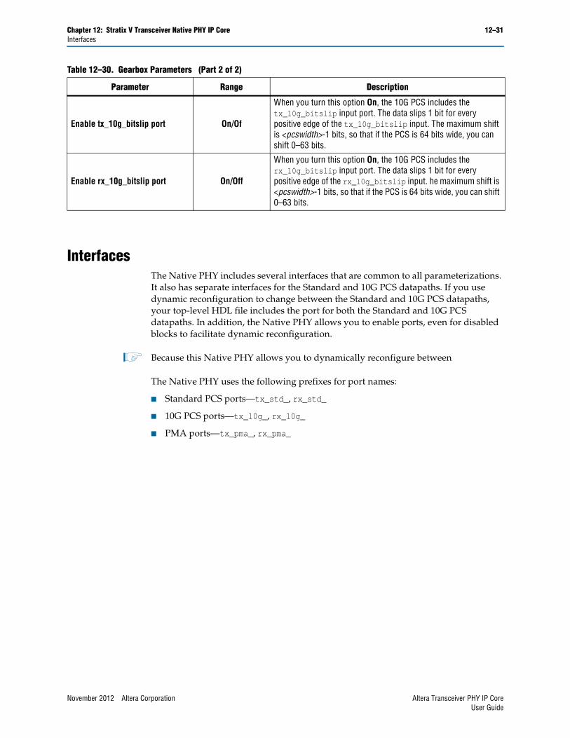
Chapter 12: Stratix V Transceiver Native PHY IP Core 12–31Interfaces
InterfacesThe Native PHY includes several interfaces that are common to all parameterizations. It also has separate interfaces for the Standard and 10G PCS datapaths. If you use dynamic reconfiguration to change between the Standard and 10G PCS datapaths, your top-level HDL file includes the port for both the Standard and 10G PCS datapaths. In addition, the Native PHY allows you to enable ports, even for disabled blocks to facilitate dynamic reconfiguration.
1 Because this Native PHY allows you to dynamically reconfigure between
The Native PHY uses the following prefixes for port names:
■ Standard PCS ports—tx_std_, rx_std_
■ 10G PCS ports—tx_10g_, rx_10g_
■ PMA ports—tx_pma_, rx_pma_
Enable tx_10g_bitslip port On/Of
When you turn this option On, the 10G PCS includes the tx_10g_bitslip input port. The data slips 1 bit for every positive edge of the tx_10g_bitslip input. The maximum shift is <pcswidth>-1 bits, so that if the PCS is 64 bits wide, you can shift 0–63 bits.
Enable rx_10g_bitslip port On/Off
When you turn this option On, the 10G PCS includes the rx_10g_bitslip input port. The data slips 1 bit for every positive edge of the rx_10g_bitslip input. he maximum shift is <pcswidth>-1 bits, so that if the PCS is 64 bits wide, you can shift 0–63 bits.
Table 12–30. Gearbox Parameters (Part 2 of 2)
Parameter Range Description
November 2012 Altera Corporation Altera Transceiver PHY IP CoreUser Guide

12–32 Chapter 12: Stratix V Transceiver Native PHY IP CoreCommon Interface Ports
The port descriptions use the following variables to represent parameters:
■ <n>—The number of lanes
■ <p>—The number of PLLs
■ <r>—the number of CDR references clocks selected
Common Interface PortsCommon interface consists of reset, clock signals, serial interface ports, control and status ports, parallel data ports, PMA ports, QPI ports, and reconfig interface ports. Figure 12–5 illustrates these ports.
Table 12–31 describes these ports.
Figure 12–5. Stratix V Native PHY Common Interfaces
tx_pll_refclk[<r>-1:0]tx_pma_clkout[<n>-1:0]rx_pma_clkout[<n>-1:0]rx_clklow[<n>-1:0]rx_fref[<n>-1:0]rx_cdr_refclk[<r>-1:0]
Clock Input& Output Signals
rx_seriallpbken[<n>-1:0]rx_setlocktodata[<n>-1:0]
rx_setlocktoref[<n>-1:0]pll_locked[<p>-1:0]
rx_is_lockedtodata[<n>-1:0]rx_is_lockedtoref[<n>-1:0]
rx_clkslip[<n>-1:0]
Control &Status Portspll_powerdown[<p>-1:0]
tx_analogreset[<n>-1:0]tx_digitalreset[<n>-1:0]rx_analogreset[<n>-1:0]rx_digitalreset[<n>-1:0]
Resets
QPI
tx_pma_parallel_data[<n>80-1:0]rx_pma_parallel_data[<n>80-1:0]tx_parallel_data[<n>64-1:0]rx_parallel_data[<n>64-1:0]
tx_pma_qpipulluptx_pma_qpipulldntx_pma_txdetectrxtx_pma_rxfoundrx_pma_qpipulldn
ParallelData Ports
tx_serial_data[<n>-1:0]rx_serial_data[<n>-1:0]
TX & RXSerial Ports
reconfig_to_xcvr [(<n>70-1):0]reconfig_from_xcvr [(<n>46-1):0]
tx_cal_busy[<n>-1:0]rx_cal_busy[<n>-1:0]
ReconfigurationInterface Ports
Native PHY Common Interfaces
Table 12–31. Native PHY Common Interfaces (Part 1 of 3)
Name Direction Description
Clock Inputs and Output Signals
tx_pll_refclk[<r>-1:0] Input The reference clock input to the TX PLL.
tx_pma_clkout[<n>-1:0] Output TX parallel clock output from PMA
rx_pma_clkout[<n>-1:0] Output RX parallel clock (recovered clock) output from PMA
rx_clklow[<n>-1:0] Output The RX recovered clock. You can use this clock as an input to an external PPM detector.
rx_fref[<n>-1:0] Output RX phase frequency detector (PFD) reference clock. You can use this clock as an input to an external PPM detector.
Altera Transceiver PHY IP Core November 2012 Altera CorporationUser Guide
Chapter 12: Stratix V Transceiver Native PHY IP Core 12–33Common Interface Ports
rx_cdr_refclk[<n>-1:0] Input Input reference clock for the RX PFD circuit.
Resets
pll_powerdown[<n>-1:0] Input When asserted, resets the TX PLL. Active high, edge sensitive reset signal.
tx_analogreset[<n>-1:0] Input When asserted, resets for TX PMA, TX clock generation block, and serializer. Active high, edge sensitive reset signal.
tx_digitalreset[<n>-1:0] Input
When asserted, resets the digital components of the TX datapath. Active high, edge sensitive reset signal.If your design includes bonded TX PCS channels, refer to Timing Constraints for Reset Signals when Using Bonded PCS Channels for a SDC constraint you must include in your design.
rx_analogreset[<n>-1:0] Input When asserted, resets the RX CDR, deserializer, Active high, edge sensitive reset signal.
rx_digitalreset[<n>-1:0] Input When asserted, resets the digital components of the RX datapath. Active high, edge sensitive reset signal.
Parallel data ports
tx_pma_parallel_data[<n>80-1:0] InputTX parallel data for the PMA Direct datapath. Driven directly from the FPGA fabric to the PMA. Not used when you enable either the Standard or 10G PCS datapath.
rx_pma_parallel_data[<n>80-1:0] OutputRX PMA parallel data driven from the PMA to the FPGA fabric. Not used when you enable either the Standard or 10G PCS datapath.
tx_parallel_data[<n>64-1:0] Input
PCS TX parallel data. Used when you enable either the Standard or 10G datapath. For the Standard datapath, if you turn on Enable simplified data interface, tx_parallel_data includes only the data and control signals necessary for the current configuration. Dynamic reconfiguration of the interface is not supported.
For the 10G PCS, if the parallel data interface is less than 64 bits wide, the low-order bits of tx_parallel_data are valid.
For the 10G PCS operating in 66:40 mode, the 66 bus is formed as follows: {tx_parallel_data[63:0],tx_10g_control[0],tx_10g_control[1]}.
rx_parallel_data[<n>64-1:0] Output
PCS RX parallel data. Used when you enable either the Standard or 10G datapath. For the Standard datapath, if you turn on Enable simplified data interface, rx_parallel_data includes only the data and control signals necessary for the current configuration. Dynamic reconfiguration of the interface is not supported.
For the 10G PCS, if the parallel data interface is less than 64 bits wide, the low-order bits of rx_parallel_data are valid.
For the 10G PCS operating in 66:40 mode, the 66 bus is formed as follows: {rx_parallel_data[63:0],rx_10g_control[0],rx_10g_control[1]}.
QPI
tx_pma_qpipullup Input QPI control input port. Only for QPI applications.
tx_pma_qpipulldn Input QPI control input port. Only for QPI applications.
Table 12–31. Native PHY Common Interfaces (Part 2 of 3)
Name Direction Description
November 2012 Altera Corporation Altera Transceiver PHY IP CoreUser Guide
12–34 Chapter 12: Stratix V Transceiver Native PHY IP CoreCommon Interface Ports
tx_pma_txdetectrx Input
When asserted, the RX detect block in the TX PMA detects the presence of a receiver at the other end of the channel. After receiving a tx_pma_txdetectrx request, the receiver detect block initiates the detection process. Only for QPI applications.
tx_pma_rxfound Output Indicates the status of an RX detection in the TX PMA. Only for QPI applications.
rx_pma_qpipulldn Input QPI control input port. Only for QPI applications.
TX and RX serial ports
tx_serial_data[<n>-1:0] Output TX differential serial output data.
rx_serial_data[<n>-1:0] Input RX differential serial output data.
Control and Status ports
rx_seriallpbken[<n>-1:0] Input When asserted, the transceiver enters loopback mode. Loopback drives TX data to the RX interface.
rx_set_locktodata[<n>-1:0] Input
When asserted, programs the RX CDR to manual lock to data mode in which you control the reset sequence using the rx_setlocktoref and rx_setlocktodata. Refer to Reset Sequence for CDR in Manual Lock Mode in Transceiver Reset Control in Stratix V Devices for more information about manual control of the reset sequence.
rx_set_locktoref[<n>-1:0] Input
When asserted, programs the RX CDR to manual lock to reference mode in which you control the reset sequence using the rx_setlocktoref and rx_setlocktodata. Refer to Reset Sequence for CDR in Manual Lock Mode in Transceiver Reset Control in Stratix V Devices for more information about manual control of the reset sequence.
pll_locked[<p>-1:0] Output When asserted, indicates that the PLL is locked to the input reference clock.
rx_is_lockedtodata[<n>-1:0] Output When asserted, the CDR is locked to the incoming data.
rx_is_lockedtoref[<n>-1:0] Output When asserted, the CDR is locked to the incoming reference clock.
rx_clkslip[<n>-1:0] Input When asserted, the deserializer slips one clock edge. This signal is used to achieve word alignment.
Reconfig Interface Ports
reconfig_to_xcvr [(<n>70-1):0] InputReconfiguration signals from the Transceiver Reconfiguration Controller. <n> grows linearly with the number of reconfiguration interfaces.
reconfig_from_xcvr [(<n>46-1):0] OutputReconfiguration signals to the Transceiver Reconfiguration Controller. <n> grows linearly with the number of reconfiguration interfaces.
tx_cal_busy[<n>-1:0] Output Reconfiguration status, indicates TX calibration is in progress
rx_cal_busy[<n>-1:0] Output Reconfiguration status, indicates RX calibration is in progress
Table 12–31. Native PHY Common Interfaces (Part 3 of 3)
Name Direction Description
Altera Transceiver PHY IP Core November 2012 Altera CorporationUser Guide

Chapter 12: Stratix V Transceiver Native PHY IP Core 12–35Standard PCS Interface Ports
Standard PCS Interface PortsFigure 12–6 illustrates the Standard PCI Interfaces. If you enable both the Standard PCS and 10G PCS your top-level HDL file includes all the interfaces for both.
Table 12–32 describes the ports available for the Standard PCS interface. When you enable both the Standard and 10G datapaths, both sets of signals are included in the top-level HDL file for the Native PHY.
1 In Table 12–32, the column labeled “Synchronous to tx_std_coreclkin/rx_std_coreclkin” applies when the phase compensation FIFO is not in register mode.
Figure 12–6. Stratix V Native PHY Standard PCS Interfaces
tx_std_clkout[<n>-1:0] rx_std_clkout[<n>-1:0]tx_std_coreclkin[<n>-1:0]rx_std_coreclkin[<n>-1:0]
ClocksWordAligner
rx_std_pcfifo_full[<n>-1:0] rx_std_pcfifo_empty[<n>-1:0] tx_std_pcfifo_full[<n>-1:0] tx_std_pcfifo_empty[<n>-1:0]
PhaseCompensation
FIFO
rx_std_byteorder_ena[<n>-1:0] rx_std_byteorder_flag[<n>-1:0]
ByteOrdering
rx_std_rmfifo_empty[<n>-1:0]rx_std_rmfifo_full[<n>-1:0]
RateMatch FIFO
rx_std_polinv[<n>-1:0]tx_std_polinv[<n>-1:0]
PolarityInversion
PMAPorts
Standard PCS Interface Ports
rx_std_bitrev_ena[<n>-1:0]tx_std_bitslipboundarysel[5<n>-1:0]rx_std_bitslipboundarysel[5<n>-1:0]
rx_std_runlength_err[<n>-1:0]rx_std_wa_patternalign[<n>-1:0]
rx_std_comdet_ena[<n>-1:0]rx_std_wa_a1a2size[<n>-1:0]
rx_std_bitslip[<n>-1:0]
tx_std_elecidle[<n>-1:0]rx_std_signaldetect[<n>-1:0]rx_std_byterev_ena[<n>-1:0]
Byte Serializer &Deserializer
Table 12–32. Standard PCS Interface Ports (Part 1 of 4)
Name DirSynchronous to
tx_std_coreclkin/rx_std_coreclkin
Description
Clocks
tx_std_clkout[<n>-1:0] Output — TX Parallel clock output as shown in the The Standard PCS Datapath figure.
rx_std_clkout[<n>-1:0] Output —RX parallel clock output as shown in The Standard PCS Datapath figure. The CDR circuitry recovers RX parallel clock from the RX data stream.
tx_std_coreclkin[<n>-1:0] Input —TX parallel clock input from the FPGA fabric that drives the write side of the TX phase compensation FIFO as shown in The Standard PCS Datapath figure.
rx_std_coreclkin[<n>-1:0] Input —RX parallel clock that drives the read side of the RX phase compensation FIFO The Standard PCS Datapath figure.
November 2012 Altera Corporation Altera Transceiver PHY IP CoreUser Guide
12–36 Chapter 12: Stratix V Transceiver Native PHY IP CoreStandard PCS Interface Ports
Phase Compensation FIFO
rx_std_pcfifo_full[<n>-1:0] Output YesRX phase compensation FIFO full status flag. Valid when the Phase Compensation FIFO is not in register mode.
rx_std_pcfifo_empty[<n>-1:0] Output YesRX phase compensation FIFO status empty flag. Valid when the Phase Compensation FIFO is not in register mode.
tx_std_pcfifo_full[<n>-1:0] Output YesTX phase compensation FIFO status full flag. Valid when the Phase Compensation FIFO is not in register mode.
tx_std_pcfifo_empty[<n>-1:0] Output YesTX phase compensation FIFO status empty flag. Valid when the Phase Compensation FIFO is not in register mode.
Byte Ordering
rx_std_byteorder_ena[<n>-1:0]
Input No
Byte ordering enable. When this signal is asserted, the byte ordering block initiates a byte ordering operation if the Byte ordering control mode is set to manual. Once byte ordering has occurred, you must deassert and reassert this signal to perform another byte ordering operation. This signal is an synchronous input signal; however, it must be asserted for at least 1 cycle of rx_std_clkout.
rx_std_byteorder_flag[<n>-1:0]
Output Yes
Byte ordering status flag. When asserted, indicates that the byte ordering block has performed a byte order operation. This signal is asserted on the clock cycle in which byte ordering occurred. This signal is synchronous to the rx_std_clkout clock. You must a synchronizer this signal.
Byte Serializer and Deserializer
rx_std_byterev_ena[<n>-1:0] Input NoThis control signals is available in when the PMA width is 16 or 20 bits. When asserted, enables byte reversal on the RX interface.
8B/10B
rx_std_polinv[<n>-1:0] Input No
Polarity inversion for the 8B/10B decoder, When set, the RX channels invert the polarity of the received data. You can use this signal to correct the polarity of differential pairs if the transmission circuitry or board layout mistakenly swapped the positive and negative signals. The polarity inversion function operates on the word aligner input.
tx_std_polinv[<n>-1:0] Input No Polarity inversion, part of 8B10B encoder, When set, the TX interface inverts the polarity of the TX data.
Table 12–32. Standard PCS Interface Ports (Part 2 of 4)
Name DirSynchronous to
tx_std_coreclkin/rx_std_coreclkin
Description
Altera Transceiver PHY IP Core November 2012 Altera CorporationUser Guide

Chapter 12: Stratix V Transceiver Native PHY IP Core 12–37Standard PCS Interface Ports
Rate Match FIFO
rx_std_rm_fifo_empty[<n>-1:0]
Output NoRate match FIFO empty flag. When asserted, the rate match FIFO is empty. You must synchronize this signal.
rx_std_rm_fifo_full[<n>-1:0] Output No Rate match FIFO full flag. When asserted the rate match FIFO is full. You must synchronize this signal.
Word Aligner
rx_std_bitrev_ena[<n>-1:0] Input No
When asserted, enables bit reversal on the RX interface. Bit order may be reversed if external transmission circuitry transmits the most significant bit first. When enabled, the receive circuitry receives all words in the reverse order. The bit reversal circuitry operates on the output of the word aligner.
tx_std_bitslipboundarysel[5<n>-1:0]
Input No Bit-Slip boundary selection signal. Specifies the number of bits that the TX bit slipper must slip.
rx_std_bitslipboundarysel[5<n>-1:0]
Output No
This signal operates when the word aligner is in bit-slip word alignment mode. It reports the number of bits that the RX block slipped to achieve deterministic latency.
rx_std_runlength_err[<n>-1:0]
Output No
When asserted, indicates a run length violation. Asserted if the number of consecutive 1s or 0s exceeds the number specified in th0e parameter editor GUI.
rx_st_wa_patternalign Input No Asserted to enable word alignment in manual word alignment mode.
rx_std_wa_a1a2size[<n>-1:0] Input No
Used for the SONET protocol. Asserted when the A1 and A2 framing bytes must be detected. A1 and A2 are SONET backplane bytes and are only used when the PMA data width is 8 bits.
rx_std_bitslip[<n>-1:0] Input No
Used when word aligner mode is bit-slip mode. For every rising edge of the rx_std_bitslip signal, the word boundary is shifted by 1 bit. Each bitslip removes the earliest received bit from the received data. You must synchronize this signal.
Table 12–32. Standard PCS Interface Ports (Part 3 of 4)
Name DirSynchronous to
tx_std_coreclkin/rx_std_coreclkin
Description
November 2012 Altera Corporation Altera Transceiver PHY IP CoreUser Guide

12–38 Chapter 12: Stratix V Transceiver Native PHY IP Core10G PCS Interface
10G PCS InterfaceFigure 12–7 illustrates the top-level signals of the 10G PCS. If you enable both the 10G PCS and Standard PCS your top-level HDL file includes all the interfaces for both.
Miscellaneous
tx_std_elecidle[<n>-1:0] Input No
When asserted, enables a circuit to detect a downstream receiver. It is used for the PCI Express protocol. This signal must be driven low when not in use because it causes the TX PMA to enter electrical idle mode with the TX serial data signals in tri-state mode.
rx_std_signaldetect[<n>-1:0] Output No
Signal threshold detect indicator required for the PCI Express protocol. When asserted, it indicates that the signal present at the receiver input buffer is above the programmed signal detection threshold value. You must synchronize this signal.
Table 12–32. Standard PCS Interface Ports (Part 4 of 4)
Name DirSynchronous to
tx_std_coreclkin/rx_std_coreclkin
Description
Figure 12–7. Stratix V Native PHY 10G PCS Interfaces
Clocks
FrameGenerator
TX FIFO
RX FIFO
BlockSynchronizer
FrameSynchronizer
Bit-SlipGearboxFeature
64B/66B
BER
10G PCS Interface Ports
CRC32
tx_10g_coreclkin[<n>-1:0]rx_10g_coreclkin[<n>-1:0]tx_10g_clkout[<n>-1:0]rx_10g_clkout[<n>-1:0]rx_10g_clk33out[<n>-1:0]t
tx_10g_control[8<n>-1:0]tx_10g_data_valid[<n>-1:0]tx_10g_fifo_full[<n>-1:0]tx_10g_fifo_pfull[<n>-1:0]tx_10g_fifo_empty[<n>-1:0]tx_10g_fifo_pempt[<n>-1:0]ytx_10g_fifo_del[<n>-1:0]tx_10g_fifo_insert[<n>-1:0]
rx_10g_control[10<n>-1:0]rx_10g_fifo_rd_en[<n>-1:0]rx_10g_data_valid[<n>-1:0]rx_10g_fifo_full[<n>-1:0]rx_10g_fifo_pfull[<n>-1:0]rx_10g_fifo_empty[<n>-1:0]rx_10g_fifo_pempty[<n>-1:0]rx_10g_fifo_align_clr[<n>-1:0]rx_10g_fifo_align_en[<n>-1:0]rx_10g_align_val[<n>-1:0]rx_10g_fifo_del[<n>-1:0]rx_10g_fifo_insert[<n>-1:0]
rx_10g_crc32err[<n>-1:0]
tx_10g_diag_status[2<n>-1:0]tx_10g_burst_en[<n>-1:0]
tx_10g_frame[<n>-1:0]
rx_10g_frame[<n>-1:0]rx_10g_frame_lock[<n>-1:0]
rx_10g_pyld_ins[<n>-1:0]rx_10g_frame_mfrm_err[<n>-1:0]rx_10g_frame_sync_err[<n>-1:0]
rx_10g_scram_err[<n>-1:0]rx_10g_frame_skip_ins[<n>-1:0]rx_10g_frame_skip_err[<n>-1:0]rx_10g_frame_diag_err[<n>-1:0]
rx_10g_frame_diag_status[2<n>-1:0]
rx_10g_blk_lock[<n>-1:0]rx_10g_blk_sh_err[<n>-1:0]
rx_10g_bitslip[<n>-1:0]tx_10g_bitslip[7<n>-1:0]
rx_10g_clr_errblk_count[<n>-1:0]
rx_10g_highber[<n>-1:0]rx_10g_clr_highber_cnt[<n>-1:0]
Altera Transceiver PHY IP Core November 2012 Altera CorporationUser Guide
Chapter 12: Stratix V Transceiver Native PHY IP Core 12–3910G PCS Interface
Table 12–33 describes the signals available for the 10G PCS datapath. When you enable both the 10G and Standard datapaths, both sets of signals are included in the top-level HDL file for the Native PHY.
1 In Table 12–33, the column labeled “Synchronous to tx_10_coreclkin/rx_10g_coreclkin” refers to cases where the phase compensation FIFO is not in register mode.
,
Table 12–33. 10G PCS Interface Ports (Part 1 of 8)
Name DirSynchronous to
tx_10g_coreclkin/rx_10g_coreclkin
Description
Clocks
tx_10g_coreclkin[<n>-1:0] Input — TX parallel clock input that drive the write side of the TX FIFO as shown in The 10G PCS datapath figure.
rx_10g_coreclkin[<n>-1:0] Input — RX parallel clock input that drives the read side of the RX FIFO as shown in The 10G PCS datapath figure.
tx_10g_clkout[<n>-1:0] Output — TX parallel clock output for the TX PCS as shown in The 10G PCS datapath figure.
rx_10g_clkout[<n>-1:0] Output — RX parallel clock output which is recovered from the RX data stream as shown in The 10G PCS datapath figure.
rx_10g_clk33out[<n>-1:0] Output — A divide by 33 clock output. You typically need this option when the fabric to PCS interface width is 66 bits.
TX FIFO
tx_10g_control[9<n>-1:0] Input Yes
TX control signals for the Interlaken, 10GBASE-R, and Basic protocols. Synchronous to tx_10g_coreclk_in. The following signals are defined:
Interlaken mode:
■ [8]: Active-high synchronous error insertion control bit
■ [7:3]: Not Used
■ [2]: Inversion signal, must always be set to 1'b0.
■ [1]: Sync Header, 1 indicates a control word
■ [0]: Sync Header, 1 indicates a data word
10G BaseR mode:
■ [8]: Active-high synchronous error insertion control signal
■ [7]: MII control signal for tx_data[63:56]
■ [6]: MII control signal for tx_data[55:48]
■ [5]: MII control signal for tx_data[47:40]
■ [4]: MII control signal for tx_data[39:32]
■ [3]: MII control signal for tx_data[31:24]
■ [2]: MII control signal for tx_data[23:16]
■ [1]: MII control signal for tx_data[15:8]
■ [0]: MII control signal for tx_data[7:0]
November 2012 Altera Corporation Altera Transceiver PHY IP CoreUser Guide

12–40 Chapter 12: Stratix V Transceiver Native PHY IP Core10G PCS Interface
tx_10g_control[9<n>-1:0](continued) Input Yes
Basic mode: 67-bit word width:
■ [8:3]: Not used
■ [2]: Inversion Bit - must always be set to 1'b0.
■ [1]: Sync Header, 1 indicates a control word)
■ [0]: Sync Header, 1 indicates a data word)
Basic mode: 66-bit word width:
■ [8:2]: Not used
■ [1]: Sync Header, 1 indicates a control word)
■ [0]: Sync Header, 1 indicates 1 data word)
Basic mode: 64-bit, 50-bit, 40-bit, 32-bit word widths:
[8:0]: Not used
tx_10g_data_valid[<n>-1:0] Input Yes
When asserted, indicates if tx_data is valid Use of this signal depends upon the protocol you are implementing, as follows:
■ 10G BASE-R: Tie to 1'b1
■ Interlaken: Acts as control for FIFO write enable. You should tie this signal to tx_10g_fifo_pempty.
■ Basic with phase compensation FIFO: Tie to 1'b1 as long as tx_coreclkin = data_rate/pld_pcs interface width. Otherwise, tie this signal to tx_10g_fifo_pempty.
■ Basic with phase compensation FIFO in register mode. This mode only allows a 1:1 gear box ratio such as 32:32 and 64:64; consequently, you can tie tx_10g_data_valid to 1’b1.
tx_10g_fifo_full[<n>-1:0] Output Yes When asserted, indicates that the TX FIFO is full. Synchronous to tx_std_clkout,
tx_10g_fifo_pfull[<n>-1:0] Output Yes When asserted, indicates that the TX FIFO is partially full.
tx_10g_fifo_empty[<n>-1:0] Output NoTX FIFO empty flag. Synchronous to tx_std_clkout. This signal is pulse-stretched; you must use a synchronizer.
tx_10g_fifo_pempty[<n>-1:0]
Output NoTX FIFO partially empty flag. Synchronous to tx_std_clkout. This signal is pulse-stretched; you must use a synchronizer.
tx_10g_fifo_del[<n>-1:0] Output YesWhen asserted, indicates that a word has been deleted from the rate match FIFO. This signal is used for the 10GBASE-R protocol.
tx_10g_fifo_insert[<n>-1:0]
Output No
When asserted, indicates that a word has been inserted into the rate match FIFO. This signal is used for the 10GBASE-R protocol. This signal is pulse-stretched, you must use a synchronizer.
Table 12–33. 10G PCS Interface Ports (Part 2 of 8)
Name DirSynchronous to
tx_10g_coreclkin/rx_10g_coreclkin
Description
Altera Transceiver PHY IP Core November 2012 Altera CorporationUser Guide
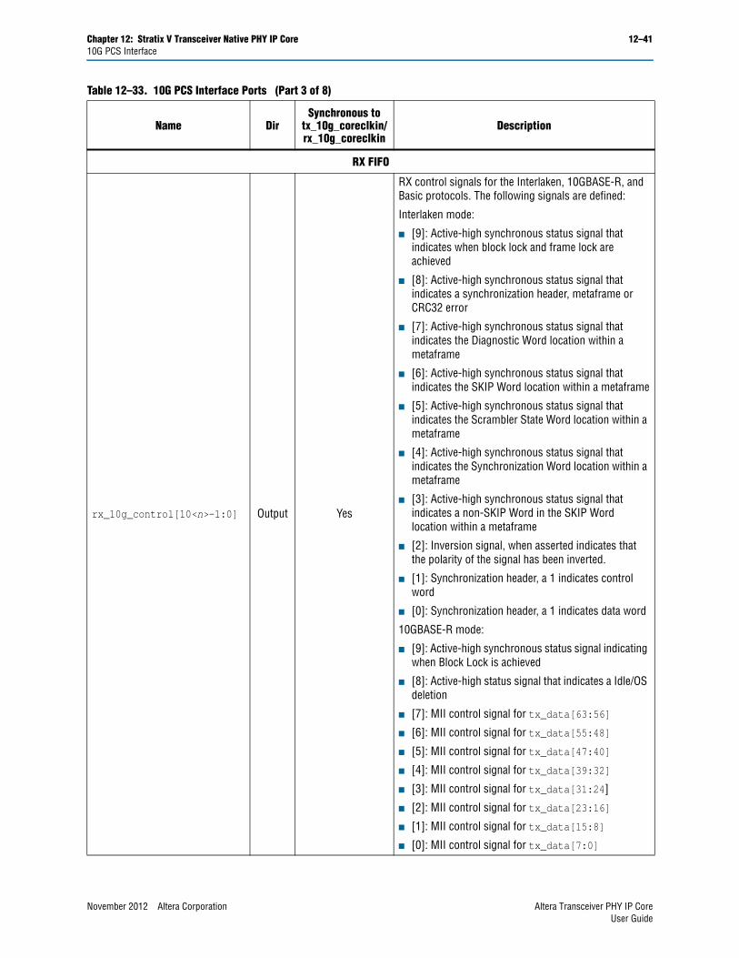
Chapter 12: Stratix V Transceiver Native PHY IP Core 12–4110G PCS Interface
RX FIFO
rx_10g_control[10<n>-1:0] Output Yes
RX control signals for the Interlaken, 10GBASE-R, and Basic protocols. The following signals are defined:
Interlaken mode:
■ [9]: Active-high synchronous status signal that indicates when block lock and frame lock are achieved
■ [8]: Active-high synchronous status signal that indicates a synchronization header, metaframe or CRC32 error
■ [7]: Active-high synchronous status signal that indicates the Diagnostic Word location within a metaframe
■ [6]: Active-high synchronous status signal that indicates the SKIP Word location within a metaframe
■ [5]: Active-high synchronous status signal that indicates the Scrambler State Word location within a metaframe
■ [4]: Active-high synchronous status signal that indicates the Synchronization Word location within a metaframe
■ [3]: Active-high synchronous status signal that indicates a non-SKIP Word in the SKIP Word location within a metaframe
■ [2]: Inversion signal, when asserted indicates that the polarity of the signal has been inverted.
■ [1]: Synchronization header, a 1 indicates control word
■ [0]: Synchronization header, a 1 indicates data word
10GBASE-R mode:
■ [9]: Active-high synchronous status signal indicating when Block Lock is achieved
■ [8]: Active-high status signal that indicates a Idle/OS deletion
■ [7]: MII control signal for tx_data[63:56]
■ [6]: MII control signal for tx_data[55:48]
■ [5]: MII control signal for tx_data[47:40]
■ [4]: MII control signal for tx_data[39:32]
■ [3]: MII control signal for tx_data[31:24]
■ [2]: MII control signal for tx_data[23:16]
■ [1]: MII control signal for tx_data[15:8]
■ [0]: MII control signal for tx_data[7:0]
Table 12–33. 10G PCS Interface Ports (Part 3 of 8)
Name DirSynchronous to
tx_10g_coreclkin/rx_10g_coreclkin
Description
November 2012 Altera Corporation Altera Transceiver PHY IP CoreUser Guide
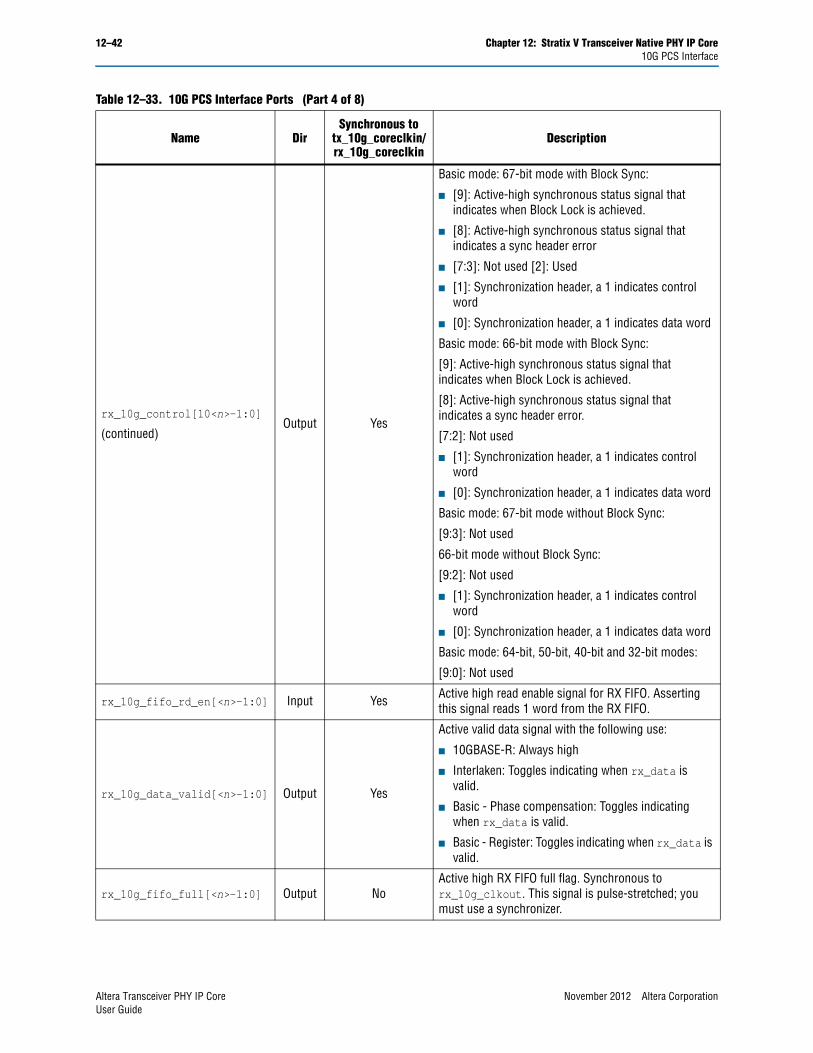
12–42 Chapter 12: Stratix V Transceiver Native PHY IP Core10G PCS Interface
rx_10g_control[10<n>-1:0]
(continued)Output Yes
Basic mode: 67-bit mode with Block Sync:
■ [9]: Active-high synchronous status signal that indicates when Block Lock is achieved.
■ [8]: Active-high synchronous status signal that indicates a sync header error
■ [7:3]: Not used [2]: Used
■ [1]: Synchronization header, a 1 indicates control word
■ [0]: Synchronization header, a 1 indicates data word
Basic mode: 66-bit mode with Block Sync:
[9]: Active-high synchronous status signal that indicates when Block Lock is achieved.
[8]: Active-high synchronous status signal that indicates a sync header error.
[7:2]: Not used
■ [1]: Synchronization header, a 1 indicates control word
■ [0]: Synchronization header, a 1 indicates data word
Basic mode: 67-bit mode without Block Sync:
[9:3]: Not used
66-bit mode without Block Sync:
[9:2]: Not used
■ [1]: Synchronization header, a 1 indicates control word
■ [0]: Synchronization header, a 1 indicates data word
Basic mode: 64-bit, 50-bit, 40-bit and 32-bit modes:
[9:0]: Not used
rx_10g_fifo_rd_en[<n>-1:0] Input Yes Active high read enable signal for RX FIFO. Asserting this signal reads 1 word from the RX FIFO.
rx_10g_data_valid[<n>-1:0] Output Yes
Active valid data signal with the following use:
■ 10GBASE-R: Always high
■ Interlaken: Toggles indicating when rx_data is valid.
■ Basic - Phase compensation: Toggles indicating when rx_data is valid.
■ Basic - Register: Toggles indicating when rx_data is valid.
rx_10g_fifo_full[<n>-1:0] Output NoActive high RX FIFO full flag. Synchronous to rx_10g_clkout. This signal is pulse-stretched; you must use a synchronizer.
Table 12–33. 10G PCS Interface Ports (Part 4 of 8)
Name DirSynchronous to
tx_10g_coreclkin/rx_10g_coreclkin
Description
Altera Transceiver PHY IP Core November 2012 Altera CorporationUser Guide
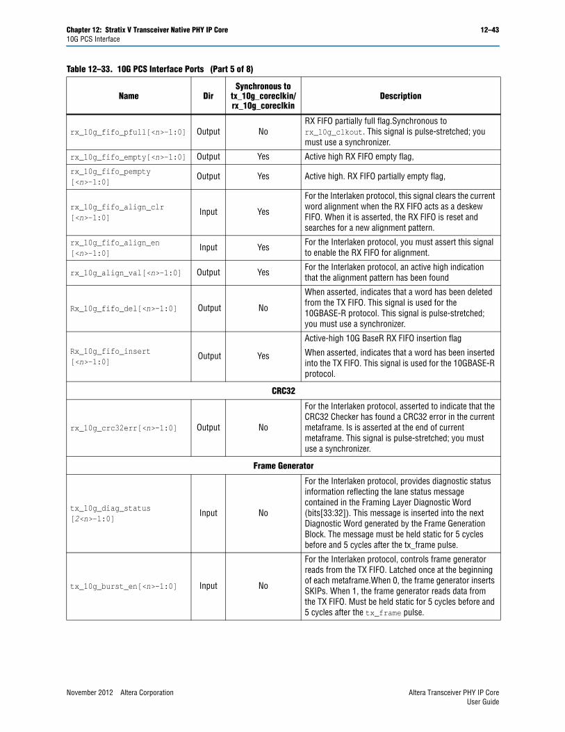
Chapter 12: Stratix V Transceiver Native PHY IP Core 12–4310G PCS Interface
rx_10g_fifo_pfull[<n>-1:0] Output NoRX FIFO partially full flag.Synchronous to rx_10g_clkout. This signal is pulse-stretched; you must use a synchronizer.
rx_10g_fifo_empty[<n>-1:0] Output Yes Active high RX FIFO empty flag,
rx_10g_fifo_pempty[<n>-1:0]
Output Yes Active high. RX FIFO partially empty flag,
rx_10g_fifo_align_clr[<n>-1:0]
Input Yes
For the Interlaken protocol, this signal clears the current word alignment when the RX FIFO acts as a deskew FIFO. When it is asserted, the RX FIFO is reset and searches for a new alignment pattern.
rx_10g_fifo_align_en[<n>-1:0]
Input Yes For the Interlaken protocol, you must assert this signal to enable the RX FIFO for alignment.
rx_10g_align_val[<n>-1:0] Output Yes For the Interlaken protocol, an active high indication that the alignment pattern has been found
Rx_10g_fifo_del[<n>-1:0] Output No
When asserted, indicates that a word has been deleted from the TX FIFO. This signal is used for the 10GBASE-R protocol. This signal is pulse-stretched; you must use a synchronizer.
Rx_10g_fifo_insert[<n>-1:0]
Output Yes
Active-high 10G BaseR RX FIFO insertion flag
When asserted, indicates that a word has been inserted into the TX FIFO. This signal is used for the 10GBASE-R protocol.
CRC32
rx_10g_crc32err[<n>-1:0] Output No
For the Interlaken protocol, asserted to indicate that the CRC32 Checker has found a CRC32 error in the current metaframe. Is is asserted at the end of current metaframe. This signal is pulse-stretched; you must use a synchronizer.
Frame Generator
tx_10g_diag_status[2<n>-1:0]
Input No
For the Interlaken protocol, provides diagnostic status information reflecting the lane status message contained in the Framing Layer Diagnostic Word (bits[33:32]). This message is inserted into the next Diagnostic Word generated by the Frame Generation Block. The message must be held static for 5 cycles before and 5 cycles after the tx_frame pulse.
tx_10g_burst_en[<n>-1:0] Input No
For the Interlaken protocol, controls frame generator reads from the TX FIFO. Latched once at the beginning of each metaframe.When 0, the frame generator inserts SKIPs. When 1, the frame generator reads data from the TX FIFO. Must be held static for 5 cycles before and 5 cycles after the tx_frame pulse.
Table 12–33. 10G PCS Interface Ports (Part 5 of 8)
Name DirSynchronous to
tx_10g_coreclkin/rx_10g_coreclkin
Description
November 2012 Altera Corporation Altera Transceiver PHY IP CoreUser Guide

12–44 Chapter 12: Stratix V Transceiver Native PHY IP Core10G PCS Interface
tx_10g_frame[<n>-1:0] Output No
For the Interlaken protocol, asserted to indicate the beginning of a new metaframe inside the frame generator. This signal is pulse-stretched; you must use a synchronizer.
Frame Synchronizer
rx_10g_frame[<n>-1:0] Output No
For the Interlaken protocol, asserted to indicate the beginning of a new metaframe inside the frame synchronizer. This signal is pulse-stretched, you must use a synchronizer. This signal is pulse-stretched; you must use a synchronizer.
rx_10g_frame_lock[<n>-1:0] Output No
For the Interlaken protocol, asserted to indicate that the frame synchronizer state machine has achieved frame lock. This signal is pulse-stretched, you must use a synchronizer. This signal is pulse-stretched; you must use a synchronizer.
Rx_10g_pyld_ins[<n>-1:0] Output No
For the Interlaken protocol, asserted to indicate a SKIP Word was not received by the frame synchronizer in a SKIP Word location within the metaframe. This signal is pulse-stretched, you must use a synchronizer. This signal is pulse-stretched; you must use a synchronizer.
rx_10g_frame_mfrm_err[<n>-1:0]
Output No
For the Interlaken protocol, asserted to indicate an error has occurred in the metaframe. This signal is pulse-stretched, you must use a synchronizer. This signal is pulse-stretched; you must use a synchronizer.
rx_10g_frame_sync_err[<n>-1:0]
Output No
For the Interlaken protocol, asserted to indicate a synchronization Control Word error was received in a synchronization Control Word location within the metaframe.
This signal is sticky if block lock is lost and does not update until block lock is re-established.This signal is pulse-stretched; you must use a synchronizer.
rx_10g_scram_err[<n>-1:0] Output No
For the Interlaken protocol, asserted to indicate, Scrambler Control Word errors in a Scrambler Control Word location within the metaframe.
This signal is sticky during the loss of block lock and does not update until block lock is re-established. This signal is pulse-stretched; you must use a synchronizer.
rx_10g_frame_skip_ins[<n>-1:0]
Output No
For the Interlaken protocol, asserted to indicate to a SKIP Word was received by the frame synchronizer in a non-SKIP Word location within the metaframe. This signal is pulse-stretched; you must use a synchronizer.
Table 12–33. 10G PCS Interface Ports (Part 6 of 8)
Name DirSynchronous to
tx_10g_coreclkin/rx_10g_coreclkin
Description
Altera Transceiver PHY IP Core November 2012 Altera CorporationUser Guide
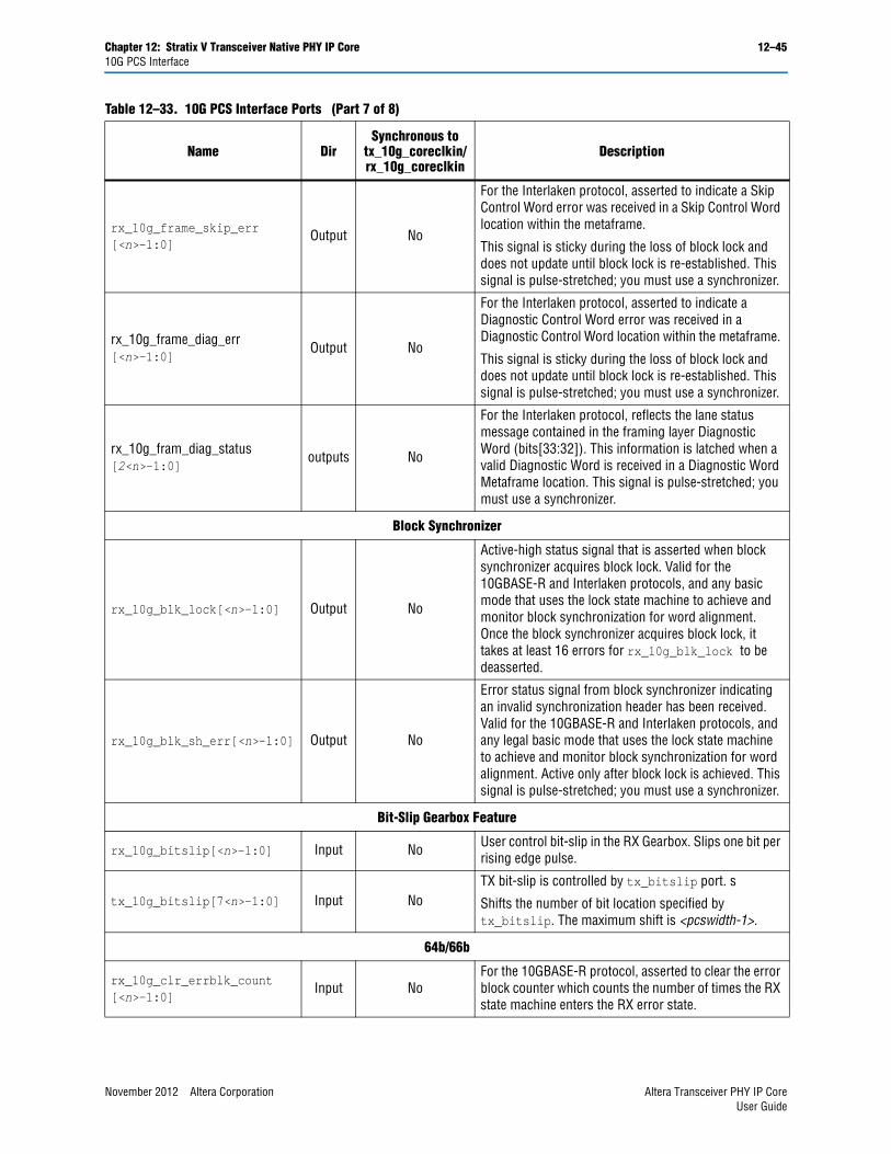
Chapter 12: Stratix V Transceiver Native PHY IP Core 12–4510G PCS Interface
rx_10g_frame_skip_err[<n>-1:0]
Output No
For the Interlaken protocol, asserted to indicate a Skip Control Word error was received in a Skip Control Word location within the metaframe.
This signal is sticky during the loss of block lock and does not update until block lock is re-established. This signal is pulse-stretched; you must use a synchronizer.
rx_10g_frame_diag_err[<n>-1:0]
Output No
For the Interlaken protocol, asserted to indicate a Diagnostic Control Word error was received in a Diagnostic Control Word location within the metaframe.
This signal is sticky during the loss of block lock and does not update until block lock is re-established. This signal is pulse-stretched; you must use a synchronizer.
rx_10g_fram_diag_status[2<n>-1:0]
outputs No
For the Interlaken protocol, reflects the lane status message contained in the framing layer Diagnostic Word (bits[33:32]). This information is latched when a valid Diagnostic Word is received in a Diagnostic Word Metaframe location. This signal is pulse-stretched; you must use a synchronizer.
Block Synchronizer
rx_10g_blk_lock[<n>-1:0] Output No
Active-high status signal that is asserted when block synchronizer acquires block lock. Valid for the 10GBASE-R and Interlaken protocols, and any basic mode that uses the lock state machine to achieve and monitor block synchronization for word alignment. Once the block synchronizer acquires block lock, it takes at least 16 errors for rx_10g_blk_lock to be deasserted.
rx_10g_blk_sh_err[<n>-1:0] Output No
Error status signal from block synchronizer indicating an invalid synchronization header has been received. Valid for the 10GBASE-R and Interlaken protocols, and any legal basic mode that uses the lock state machine to achieve and monitor block synchronization for word alignment. Active only after block lock is achieved. This signal is pulse-stretched; you must use a synchronizer.
Bit-Slip Gearbox Feature
rx_10g_bitslip[<n>-1:0] Input No User control bit-slip in the RX Gearbox. Slips one bit per rising edge pulse.
tx_10g_bitslip[7<n>-1:0] Input NoTX bit-slip is controlled by tx_bitslip port. s
Shifts the number of bit location specified by tx_bitslip. The maximum shift is <pcswidth-1>.
64b/66b
rx_10g_clr_errblk_count[<n>-1:0]
Input NoFor the 10GBASE-R protocol, asserted to clear the error block counter which counts the number of times the RX state machine enters the RX error state.
Table 12–33. 10G PCS Interface Ports (Part 7 of 8)
Name DirSynchronous to
tx_10g_coreclkin/rx_10g_coreclkin
Description
November 2012 Altera Corporation Altera Transceiver PHY IP CoreUser Guide
12–46 Chapter 12: Stratix V Transceiver Native PHY IP CoreSDC Timing Constraints
SDC Timing Constraints The Quartus II 12.1 software reports timing violations for asynchronous inputs to the Standard PCS and 10G PCS. Because many violations are for asynchronous paths, they do not represent actual timing failures. You may choose one of the following three approaches to identify these false timing paths to the Quartus II or TimeQuest software.
■ You can cut these paths in your Synopsys Design Constraints (.sdc) file by using the set_false_path command as shown in Example 12–1.
BER
rx_10g_highber[<n>-1:0] Output No
For the 10GBASE-R protocol, status signal asserted to indicate a bit error ratio of >10–4. A count of 16 in 125us indicates a bit error ratio of >10–4. Once asserted, it remains high for at least 125 s.
rx_10g_clr_highber_cnt[<n>-1:0]
Input No
For the 10GBASE-R protocol, status signal asserted to clear the BER counter which counts the number of times the BER state machine enters the BER_BAD_SH state. This signal has no effect on the operation of the BER state machine.
Table 12–33. 10G PCS Interface Ports (Part 8 of 8)
Name DirSynchronous to
tx_10g_coreclkin/rx_10g_coreclkin
Description
Example 12–1. Using the set_false_path Constraint to Identify Asynchronous Inputs
set_false_path -through {*10gtxbursten*} -to [get_registers *10g_tx_pcs*SYNC_DATA_REG*]set_false_path -through {*10gtxdiagstatus*} -to [get_registers *10g_tx_pcs*SYNC_DATA_REG*]set_false_path -through {*10gtxwordslip*} -to [get_registers *10g_tx_pcs*SYNC_DATA_REG*]set_false_path -through {*10gtxbitslip*} -to [get_registers *10g_tx_pcs*SYNC_DATA_REG*]set_false_path -through {*10grxbitslip*} -to [get_registers *10g_rx_pcs*SYNC_DATA_REG*]set_false_path -through {*10grxclrbercount*} -to [get_registers *10g_rx_pcs*SYNC_DATA_REG*] set_false_path -through {*10grxclrerrblkcnt*} -to [get_registers *10g_rx_pcs*SYNC_DATA_REG*] set_false_path -through {*10grxprbserrclr*} -to [get_registers *10g_rx_pcs*SYNC_DATA_REG*]
set_false_path -through {*8gbitslip*} -to [get_registers *8g_rx_pcs*SYNC_DATA_REG*]set_false_path -through {*8gbytordpld*} -to [get_registers *8g_rx_pcs*SYNC_DATA_REG*] set_false_path -through {*8gcmpfifoburst*} -to [get_registers *8g_rx_pcs*SYNC_DATA_REG*] set_false_path -through {*8gphfifoburstrx*} -to [get_registers *8g_rx_pcs*SYNC_DATA_REG*]
set_false_path -through {*8gsyncsmen*} -to [get_registers *8g*pcs*SYNC_DATA_REG*]set_false_path -through {*8gwrdisablerx*} -to [get_registers *8g_rx_pcs*SYNC_DATA_REG*] set_false_path -through {*rxpolarity*} -to [get_registers *SYNC_DATA_REG*]set_false_path -through {*pldeidleinfersel*} -to [get_registers *SYNC_DATA_REG*]
Altera Transceiver PHY IP Core November 2012 Altera CorporationUser Guide
Chapter 12: Stratix V Transceiver Native PHY IP Core 12–47Dynamic Reconfiguration
■ You can use the set_max_delay constraint on a given path to create a constraint for asynchronous signals that do not have a specific clock relationship but require a maximum path delay. Example 12–2 illustrates this approach.
■ You can use the set_false path command only during Timequest timing analysis. Example 12–3 illustrates this approach.
1 In in all of these examples, you must substitute you actual signal names for the signal names shown.
Dynamic Reconfiguration As silicon progresses towards smaller process nodes, circuit performance is affected more by variations due to process, voltage, and temperature (PVT). These process variations result in analog voltages that can be offset from required ranges. The calibration performed by the dynamic reconfiguration interface compensates for variations due to PVT.
For non-bonded clocks, each channel and each TX PLL has a separate dynamic reconfiguration interfaces. The MegaWizard Plug-In Manager provides informational messages on the connectivity of these interfaces. Example 12–4 shows the messages for the Stratix V Native PHY with four duplex channels, four TX PLLs, in a non-bonded configuration.
For more information about transceiver reconfiguration refer to Chapter 16, Transceiver Reconfiguration Controller IP Core.
If you are using ×6 or ×N bonding, transceiver dynamic reconfiguration requires that you assign the starting channel number. Logical channel 0 should be assigned to either physical transceiver channel 1 or channel 4 of a transceiver bank. However, if you have already created a PCB with a different lane assignment for logical lane 0, you can use the workaound shown in Example 12–5 to remove this restriction. Example 12–5 redefines the pma_bonding_master parameter using the Quartus II
Example 12–2. Using the mandala Constraint to Identify Asynchronous Inputs
# Example: Apply 10ns max delayset_max_delay -from *tx_from_fifo* -to *8g*pcs*SYNC_DATA_REG1 10
Example 12–3. Using the set_false TimeQuest Constraint to Identify Asynchronous Inputs
#if {$::TimeQuestInfo(nameofexecutable) eq "quartus_fit"} { #} else {#set_false_path -from [get_registers {*tx_from_fifo*}] -through {*txbursten*} -to [get_registers *8g_*_pcs*SYNC_DATA_REG
Example 12–4. Informational Messages for the Transceiver Reconfiguration Interface
PHY IP will require 8 reconfiguration interfaces for connection to the external reconfiguration controller.Reconfiguration interface offsets 0-3 are connected to the transceiver channels.Reconfiguration interface offsets 4–7 are connected to the transmit PLLs.
November 2012 Altera Corporation Altera Transceiver PHY IP CoreUser Guide

12–48 Chapter 12: Stratix V Transceiver Native PHY IP CoreSimulation Support
Assignment Editor. In this example, the pma_bonding_master was originally assigned to physical channel 1. (The original assignment could also have been to physical channel 4.) The to parameter reassigns the pma_bonding_master to the Deterministic Latency PHY instance name. You must substitute the instance name from your design for the instance name shown in quotation marks
Simulation SupportThe Quartus II 12.1 release provides simulation and compilation support for the Stratix V Native PHY IP Core. Refer to Running a Simulation Testbench for a description of the directories and files that the Quartus II software creates automatically when you generate your Stratix V Transceiver Native PHY IP Core.
Example 12–5. Overriding Logical Channel 0 Channel Assignment Restrictions in Stratix V Device for ×6 or ×N Bonding
set_parameter -name pma_bonding_master "\"1\"" -to "<PHY IP instance name>"
Altera Transceiver PHY IP Core November 2012 Altera CorporationUser Guide
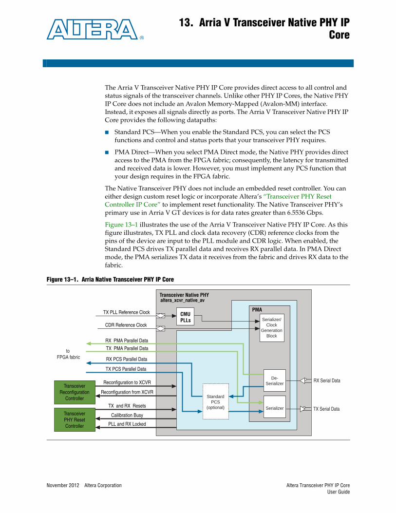
November 2012 Altera Corporation
13. Arria V Transceiver Native PHY IPCore
The Arria V Transceiver Native PHY IP Core provides direct access to all control and status signals of the transceiver channels. Unlike other PHY IP Cores, the Native PHY IP Core does not include an Avalon Memory-Mapped (Avalon-MM) interface. Instead, it exposes all signals directly as ports. The Arria V Transceiver Native PHY IP Core provides the following datapaths:
■ Standard PCS—When you enable the Standard PCS, you can select the PCS functions and control and status ports that your transceiver PHY requires.
■ PMA Direct—When you select PMA Direct mode, the Native PHY provides direct access to the PMA from the FPGA fabric; consequently, the latency for transmitted and received data is lower. However, you must implement any PCS function that your design requires in the FPGA fabric.
The Native Transceiver PHY does not include an embedded reset controller. You can either design custom reset logic or incorporate Altera’s “Transceiver PHY Reset Controller IP Core” to implement reset functionality. The Native Transceiver PHY’s primary use in Arria V GT devices is for data rates greater than 6.5536 Gbps.
Figure 13–1 illustrates the use of the Arria V Transceiver Native PHY IP Core. As this figure illustrates, TX PLL and clock data recovery (CDR) reference clocks from the pins of the device are input to the PLL module and CDR logic. When enabled, the Standard PCS drives TX parallel data and receives RX parallel data. In PMA Direct mode, the PMA serializes TX data it receives from the fabric and drives RX data to the fabric.
Figure 13–1. Arria Native Transceiver PHY IP Core
CMUPLLs
PMA
altera_xcvr_native_av Transceiver Native PHY
Reconfiguration to XCVR
Reconfiguration from XCVR
TX and RX Resets
Calilbration Busy
PLL and RX Locked
RX PCS Parallel Data
TX PCS Parallel Data
CDR Reference Clock
TX PLL Reference Clock
RX Serial Data
to FPGA fabric
TX PMA Parallel Data
RX PMA Parallel Data
TX Serial DataSerializer
De-Serializer
StandardPCS
(optional)
Serializer/Clock
GenerationBlock
TransceiverReconfiguration
Controller
TransceiverPHY ResetController
Altera Transceiver PHY IP CoreUser Guide
13–2 Chapter 13: Arria V Transceiver Native PHY IP CoreDevice Family Support
In a typical design, the separately instantiated Transceiver PHY Reset Controller drives reset signals to Native PHY and receives calibration and locked status signal from the Native PHY. The Native PHY reconfiguration buses connect the external Transceiver Reconfiguration Controller for calibration and dynamic reconfiguration of the channel and PLLs.
You specify the initial configuration when you parameterize the IP core. The Transceiver Native PHY IP Core connects to the “Transceiver Reconfiguration Controller IP Core” to dynamically change reference clocks, PLL connectivity, and the channel configurations at runtime.
Device Family SupportIP cores provide either final or preliminary support for target Altera device families. These terms have the following definitions:
■ Final support—Verified with final timing models for this device.
■ Preliminary support—Verified with preliminary timing models for this device.
Table 13–1 shows the level of support offered by the Arria V Transceiver Native PHY IP Core for Altera device families.
Performance and Resource UtilizationBecause the Standard PCS and PMA are implemented in hard logic, the Arria V Native PHY IP Core requires minimal resources.
Parameterizing the Arria V Native PHYBy default, the Arria V Native PHY Transceiver PHY IP defaults to the PMA direct datapath and an internal PLL. You can change the default configuration to include the PCS or an external fractional PLL using the MegaWizard Plug-In Manager.
1. For Which device family will you be using?, select Arria V from the list.
2. Click Installed Plug-Ins > Interfaces > Transceiver PHY > Arria V Native PHY v12.1.
3. Use the tabs on the MegaWizard Plug-In Manager to select the options required for the protocol.
4. Click Finish to generate your customized Arria V Native PHY IP Core.
1 The Arria V Transceiver Native PHY provides presets for CPRI, GIGE, and the Low Latency Standard PCS. The presets specify the parameters required to the protocol specified.
Table 13–1. Device Family Support
Device Family Support
Arria V devices Preliminary
Other device families No support
Altera Transceiver PHY IP Core November 2012 Altera CorporationUser Guide
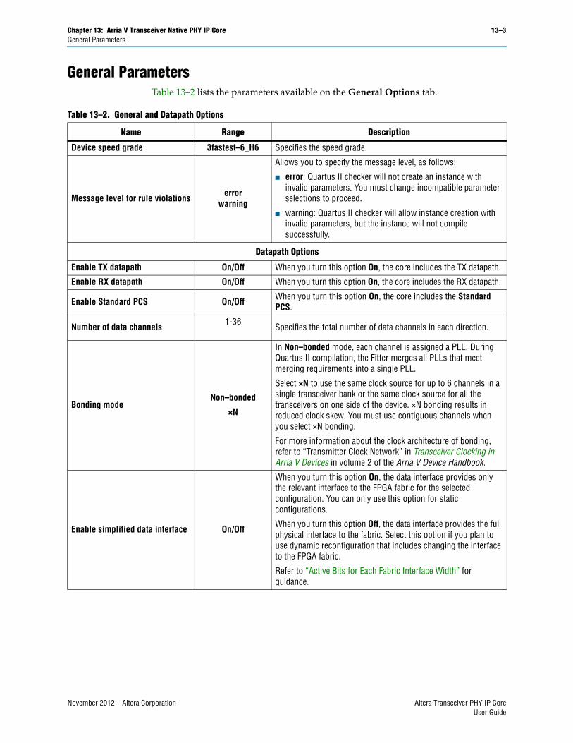
Chapter 13: Arria V Transceiver Native PHY IP Core 13–3General Parameters
General ParametersTable 13–2 lists the parameters available on the General Options tab.
Table 13–2. General and Datapath Options
Name Range Description
Device speed grade 3fastest–6_H6 Specifies the speed grade.
Message level for rule violations errorwarning
Allows you to specify the message level, as follows:
■ error: Quartus II checker will not create an instance with invalid parameters. You must change incompatible parameter selections to proceed.
■ warning: Quartus II checker will allow instance creation with invalid parameters, but the instance will not compile successfully.
Datapath Options
Enable TX datapath On/Off When you turn this option On, the core includes the TX datapath.
Enable RX datapath On/Off When you turn this option On, the core includes the RX datapath.
Enable Standard PCS On/Off When you turn this option On, the core includes the Standard PCS.
Number of data channels 1-36 Specifies the total number of data channels in each direction.
Bonding modeNon–bonded
×N
In Non–bonded mode, each channel is assigned a PLL. During Quartus II compilation, the Fitter merges all PLLs that meet merging requirements into a single PLL.
Select ×N to use the same clock source for up to 6 channels in a single transceiver bank or the same clock source for all the transceivers on one side of the device. ×N bonding results in reduced clock skew. You must use contiguous channels when you select ×N bonding.
For more information about the clock architecture of bonding, refer to “Transmitter Clock Network” in Transceiver Clocking in Arria V Devices in volume 2 of the Arria V Device Handbook.
Enable simplified data interface On/Off
When you turn this option On, the data interface provides only the relevant interface to the FPGA fabric for the selected configuration. You can only use this option for static configurations.
When you turn this option Off, the data interface provides the full physical interface to the fabric. Select this option if you plan to use dynamic reconfiguration that includes changing the interface to the FPGA fabric.
Refer to “Active Bits for Each Fabric Interface Width” for guidance.
November 2012 Altera Corporation Altera Transceiver PHY IP CoreUser Guide

13–4 Chapter 13: Arria V Transceiver Native PHY IP CorePMA Parameters
PMA ParametersTable 13–3 describes the options available for the PMA.
f For more information about the PMA, refer to the PMA Architecture section in the Transceiver Architecture in Arria V Devices.Some parameters have ranges where the value is specified as Device Dependent. For such parameters, the possible range of frequencies and bandwidths depends on the device, speed grade, and other design characteristics. Refer to Device Datasheet for Arria V Devices for specific data for Arria V devices.
TX PMA ParametersTable 13–4 describes the TX PMA options you can specify.
f For more information about PLLs in Arria V devices, refer to the Arria V PLLs section in Clock Networks and PLLs in Arria V Devices.
Table 13–3. PMA Options
Parameter Range Description
Data rate Device Dependent Specifies the data rate. The maximum data rate is 12.5 Gbps.
PMA direct interface width 8.10,16,20,64,80 Specifies the PMA to FPGA fabric interface width for PMA Direct mode.
TX local clock division factor 1, 2, 4, 8
Specifies the value of the divider available in the transceiver channels to divide the input clock to generate the correct frequencies for the parallel and serial clocks. This divisor divides the fast clock from the PLL in non-bonded configurations.
PLL base data rate Device Dependent
Shows the base data rate of the clock input to the TX PLL.The PLL base data rate is computed from the TX local clock division factor multiplied by the data rate.
Select a PLL base data rate that minimizes the number of PLLs required to generate all the clocks for data transmission. By selecting an appropriate PLL base data rate, you can change data rates by changing the TX local clock division factor used by the clock generation block.
Table 13–4. TX PMA Parameters
Parameter Range Description
Enable TX PLL dynamic reconfiguration On/Off
When you turn this option On, you can dynamically reconfigure the PLL. This option is also required to simulate TX PLL reconfiguration. If you turn this option On, the Quartus II Fitter prevents PLL merging by default; however, you can specify merging using the FORCE_MERGE_PLL QSF assignments.
Use external TX PLL On/Off
When you turn this option On, the Native PHY does not include TX PLLs. Instead, the Native PHY includes a input clock port for connection to the fast clock from an external PLL, ext_pll_clk[<p>-1:0] that you can connect to external PLLs. Use feature when need to perform TX PLL switching between fractional PLL and a CMU PLL.
Altera Transceiver PHY IP Core November 2012 Altera CorporationUser Guide
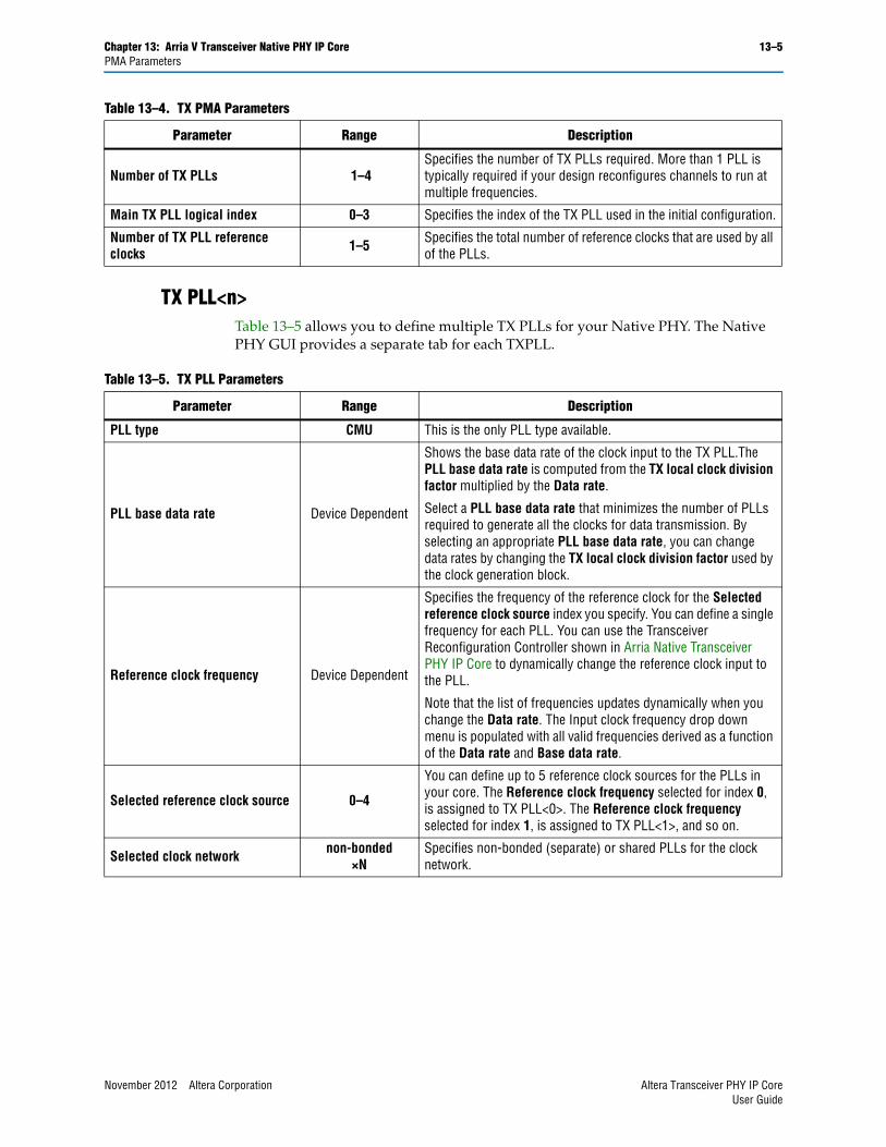
Chapter 13: Arria V Transceiver Native PHY IP Core 13–5PMA Parameters
TX PLL<n>Table 13–5 allows you to define multiple TX PLLs for your Native PHY. The Native PHY GUI provides a separate tab for each TXPLL.
Number of TX PLLs 1–4Specifies the number of TX PLLs required. More than 1 PLL is typically required if your design reconfigures channels to run at multiple frequencies.
Main TX PLL logical index 0–3 Specifies the index of the TX PLL used in the initial configuration.
Number of TX PLL reference clocks 1–5 Specifies the total number of reference clocks that are used by all
of the PLLs.
Table 13–4. TX PMA Parameters
Parameter Range Description
Table 13–5. TX PLL Parameters
Parameter Range Description
PLL type CMU This is the only PLL type available.
PLL base data rate Device Dependent
Shows the base data rate of the clock input to the TX PLL.The PLL base data rate is computed from the TX local clock division factor multiplied by the Data rate.
Select a PLL base data rate that minimizes the number of PLLs required to generate all the clocks for data transmission. By selecting an appropriate PLL base data rate, you can change data rates by changing the TX local clock division factor used by the clock generation block.
Reference clock frequency Device Dependent
Specifies the frequency of the reference clock for the Selected reference clock source index you specify. You can define a single frequency for each PLL. You can use the Transceiver Reconfiguration Controller shown in Arria Native Transceiver PHY IP Core to dynamically change the reference clock input to the PLL.
Note that the list of frequencies updates dynamically when you change the Data rate. The Input clock frequency drop down menu is populated with all valid frequencies derived as a function of the Data rate and Base data rate.
Selected reference clock source 0–4
You can define up to 5 reference clock sources for the PLLs in your core. The Reference clock frequency selected for index 0, is assigned to TX PLL<0>. The Reference clock frequency selected for index 1, is assigned to TX PLL<1>, and so on.
Selected clock network non-bonded×N
Specifies non-bonded (separate) or shared PLLs for the clock network.
November 2012 Altera Corporation Altera Transceiver PHY IP CoreUser Guide
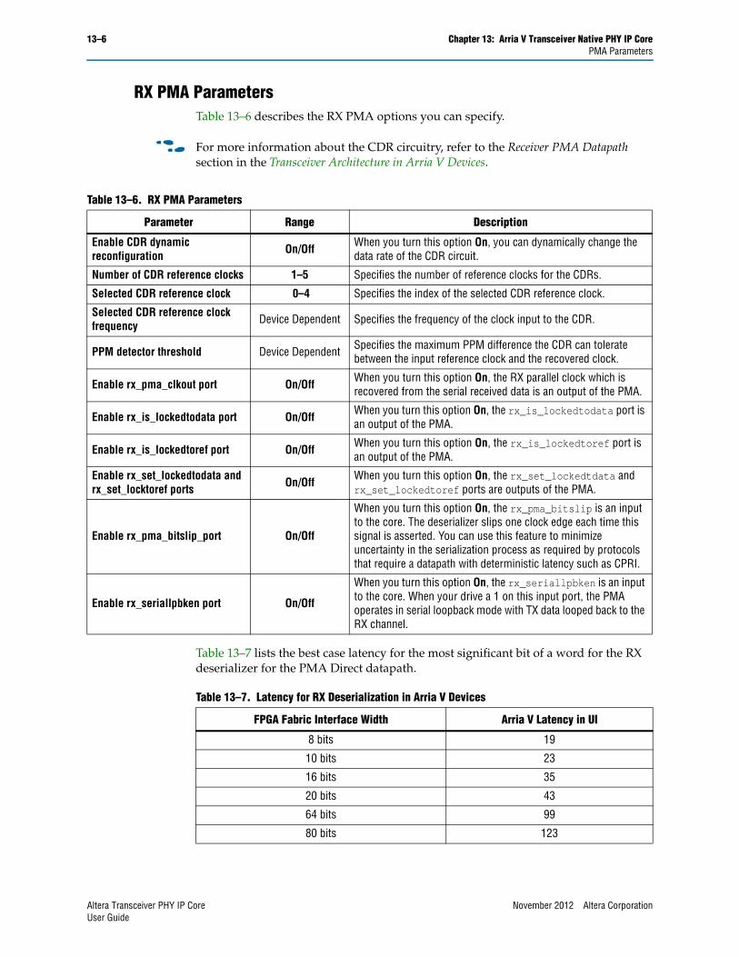
13–6 Chapter 13: Arria V Transceiver Native PHY IP CorePMA Parameters
RX PMA Parameters Table 13–6 describes the RX PMA options you can specify.
f For more information about the CDR circuitry, refer to the Receiver PMA Datapath section in the Transceiver Architecture in Arria V Devices.
Table 13–7 lists the best case latency for the most significant bit of a word for the RX deserializer for the PMA Direct datapath.
Table 13–6. RX PMA Parameters
Parameter Range Description
Enable CDR dynamic reconfiguration On/Off When you turn this option On, you can dynamically change the
data rate of the CDR circuit.
Number of CDR reference clocks 1–5 Specifies the number of reference clocks for the CDRs.
Selected CDR reference clock 0–4 Specifies the index of the selected CDR reference clock.
Selected CDR reference clock frequency Device Dependent Specifies the frequency of the clock input to the CDR.
PPM detector threshold Device Dependent Specifies the maximum PPM difference the CDR can tolerate between the input reference clock and the recovered clock.
Enable rx_pma_clkout port On/Off When you turn this option On, the RX parallel clock which is recovered from the serial received data is an output of the PMA.
Enable rx_is_lockedtodata port On/Off When you turn this option On, the rx_is_lockedtodata port is an output of the PMA.
Enable rx_is_lockedtoref port On/Off When you turn this option On, the rx_is_lockedtoref port is an output of the PMA.
Enable rx_set_lockedtodata and rx_set_locktoref ports On/Off When you turn this option On, the rx_set_lockedtdata and
rx_set_lockedtoref ports are outputs of the PMA.
Enable rx_pma_bitslip_port On/Off
When you turn this option On, the rx_pma_bitslip is an input to the core. The deserializer slips one clock edge each time this signal is asserted. You can use this feature to minimize uncertainty in the serialization process as required by protocols that require a datapath with deterministic latency such as CPRI.
Enable rx_seriallpbken port On/Off
When you turn this option On, the rx_seriallpbken is an input to the core. When your drive a 1 on this input port, the PMA operates in serial loopback mode with TX data looped back to the RX channel.
Table 13–7. Latency for RX Deserialization in Arria V Devices
FPGA Fabric Interface Width Arria V Latency in UI
8 bits 19
10 bits 23
16 bits 35
20 bits 43
64 bits 99
80 bits 123
Altera Transceiver PHY IP Core November 2012 Altera CorporationUser Guide
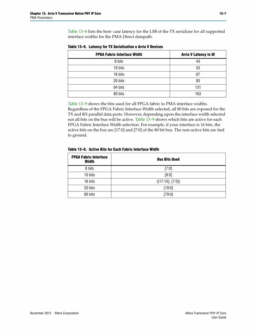
Chapter 13: Arria V Transceiver Native PHY IP Core 13–7PMA Parameters
Table 13–8 lists the best- case latency for the LSB of the TX serializer for all supported interface widths for the PMA Direct datapath.
Table 13–9 shows the bits used for all FPGA fabric to PMA interface widths. Regardless of the FPGA Fabric Interface Width selected, all 80 bits are exposed for the TX and RX parallel data ports. However, depending upon the interface width selected not all bits on the bus will be active. Table 13–9 shows which bits are active for each FPGA Fabric Interface Width selection. For example, if your interface is 16 bits, the active bits on the bus are [17:0] and [7:0] of the 80 bit bus. The non-active bits are tied to ground.
Table 13–8. Latency for TX Serialization n Arria V Devices
FPGA Fabric Interface Width Arria V Latency in UI
8 bits 43
10 bits 53
16 bits 67
20 bits 83
64 bits 131
80 bits 163
Table 13–9. Active Bits for Each Fabric Interface Width
FPGA Fabric Interface Width Bus Bits Used
8 bits [7:0]
10 bits [9:0]
16 bits {[17:10], [7:0]}
20 bits [19:0]
80 bits [79:0]
November 2012 Altera Corporation Altera Transceiver PHY IP CoreUser Guide
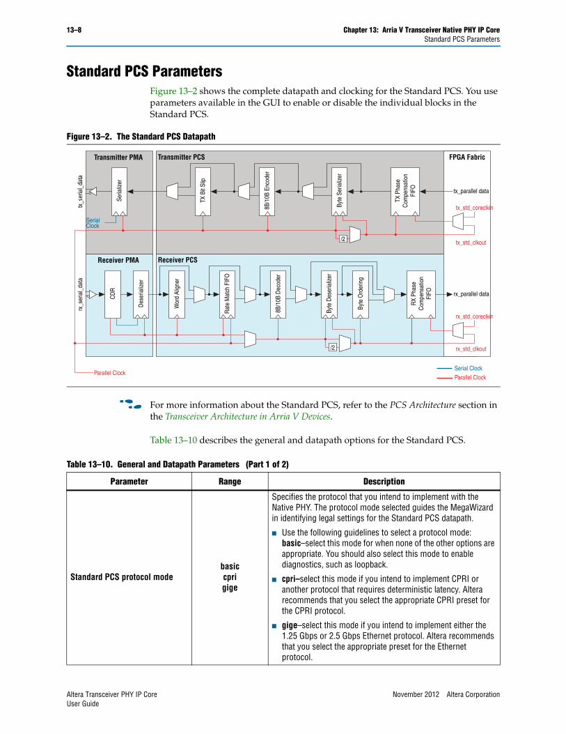
13–8 Chapter 13: Arria V Transceiver Native PHY IP CoreStandard PCS Parameters
Standard PCS ParametersFigure 13–2 shows the complete datapath and clocking for the Standard PCS. You use parameters available in the GUI to enable or disable the individual blocks in the Standard PCS.
f For more information about the Standard PCS, refer to the PCS Architecture section in the Transceiver Architecture in Arria V Devices.
Table 13–10 describes the general and datapath options for the Standard PCS.
Figure 13–2. The Standard PCS Datapath
Transmitter PCSTransmitter PMA
Receiver PMA Receiver PCS
FPGA Fabric
Byte
Ord
erin
g
RX
Phas
eC
ompe
nsat
ion
FIFO
Byte
Des
eria
lizer
8B/1
0B D
ecod
er
Rat
e M
atch
FIF
O
Wor
d Al
igne
r
Des
eria
lizer
CD
R
TX P
hase
Com
pens
atio
nFI
FO
Byte
Ser
ializ
er
8B/1
0B E
ncod
er
TX B
it Sl
ip
Seria
lizer
rx_s
eria
l_da
tatx_
seria
l_data
tx_parallel data
rx_parallel data
/2
/2
tx_std_coreclkin
rx_std_coreclkin
Parallel Clock
SerialClock
Serial ClockParallel Clock
tx_std_clkout
rx_std_clkout
Table 13–10. General and Datapath Parameters (Part 1 of 2)
Parameter Range Description
Standard PCS protocol modebasiccprigige
Specifies the protocol that you intend to implement with the Native PHY. The protocol mode selected guides the MegaWizard in identifying legal settings for the Standard PCS datapath.
■ Use the following guidelines to select a protocol mode: basic–select this mode for when none of the other options are appropriate. You should also select this mode to enable diagnostics, such as loopback.
■ cpri–select this mode if you intend to implement CPRI or another protocol that requires deterministic latency. Altera recommends that you select the appropriate CPRI preset for the CPRI protocol.
■ gige–select this mode if you intend to implement either the 1.25 Gbps or 2.5 Gbps Ethernet protocol. Altera recommends that you select the appropriate preset for the Ethernet protocol.
Altera Transceiver PHY IP Core November 2012 Altera CorporationUser Guide
Chapter 13: Arria V Transceiver Native PHY IP Core 13–9Standard PCS Parameters
Phase Compensation FIFOThe phase compensation FIFO assures clean data transfer to and from the FPGA fabric by compensating for the clock phase difference between the low-speed parallel clock and FPGA fabric interface clock. Table 13–11 describes the options for the phase compensation FIFO.
f For more information refer to the Receiver Phase Compensation FIFO and Transmitter Phase Compensation FIFO sections in the Transceiver Architecture in Arria V Devices.
Standard PCS/PMA interface width 8, 10,16, 20
Specifies the width of the datapath that connects the FPGA fabric to the PMA. The transceiver interface width depends upon whether you enable 8B/10B. To simplify connectivity between the FPGA fabric and PMA, the bus bits used are not contiguous for 16- and 32-bit buses. Refer to Active Bits for Each Fabric Interface Width for the bits used.
FPGA fabric/Standard TX PCS interface width
8, 10,16, 20, 32, 40
Shows the FPGA fabric to TX PCS interface width which is calculated from the Standard PCS/PMA interface width.
FPGA fabric/Standard RX PCS interface width
8, 10,16, 20, 32, 40
Shows the FPGA fabric to RX PCS interface width which is calculated from the Standard PCS/PMA interface width.
Enable ‘Standard PCS’ low latency mode On/Off
When you turn this option On, all PCS functions are disabled except for the phase compensation FIFO, byte serializer and byte deserializer. This option creates the lowest latency Native PHY that allows dynamic reconfigure between multiple PCS datapaths.
Table 13–10. General and Datapath Parameters (Part 2 of 2)
Parameter Range Description
Table 13–11. Phase Compensation FIFO Parameters
Parameter Range Description
TX FIFO mode low_latencyregister_fifo
The following 2 modes are possible:
■ low_latency: This mode adds 3–4 cycles of latency to the TX datapath.
■ register_fifo: In this mode the FIFO is replaced by registers to reduce the latency through the PCS. Use this mode for protocols that require deterministic latency, such as CPRI.
RX FIFO mode low_latencyregister_fifo
The following 2 modes are possible:
■ low_latency: This mode adds 2–3 cycles of latency to the TX datapath.
■ register_fifo: In this mode the FIFO is replaced by registers to reduce the latency through the PCS. Use this mode for protocols that require deterministic latency, such as CPRI.
Enable tx_std_pcfifo_full port On/Off When you turn this option On, the TX Phase compensation FIFO outputs a FIFO full status flag.
Enable tx_std_pcfifo_empty port On/Off When you turn this option On, the TX Phase compensation FIFO outputs a FIFO empty status flag.
Enable rx_std_pcfifo_full port On/Off When you turn this option On, the RX Phase compensation FIFO outputs a FIFO full status flag.
November 2012 Altera Corporation Altera Transceiver PHY IP CoreUser Guide
13–10 Chapter 13: Arria V Transceiver Native PHY IP CoreStandard PCS Parameters
Byte Ordering Block ParametersThe RX byte ordering block realigns the data coming from the byte deserializer. This block is necessary when the PCS to FPGA fabric interface width is greater than the PCS datapath. Because the timing of the RX PCS reset logic is indeterminate, the byte ordering at the output of the byte deserializer may or may not match the original byte ordering of the transmitted data. Table 13–12 describes the byte ordering block parameters.For more information refer to the Byte Ordering section in the Transceiver Architecture in Arria V Devices.
Enable rx_std_pcfifo_empty port On/Off When you turn this option On, the RX Phase compensation FIFO outputs a FIFO empty status flag.
Enable rx_std_rmfifo_empty port On/Off
When you turn this option On, the rate match FIFO outputs a FIFO empty status flag. The rate match FIFO compensates for small clock frequency differences between the upstream transmitter and the local receiver clocks by inserting or removing skip (SKP) symbols or ordered sets from the inter-packet gap (IPG) or idle stream.
Enable rx_std_rmfifo_full port On/Off When you turn this option On, the rate match FIFO outputs a FIFO full status flag.
Table 13–11. Phase Compensation FIFO Parameters
Parameter Range Description
Table 13–12. Byte Ordering Block Parameters (Part 1 of 2)
Parameter Range Description
Enable RX byte ordering On/Off When you turn this option On, the PCS includes the byte ordering block.
Byte ordering control mode manualauto
Specifies the control mode for the byte ordering block. The following modes are available:
■ Manual: Allows you to control the byte ordering block
■ Auto: The word aligner automatically controls the byte ordering block once word alignment is achieved.
Byte ordering pattern width 8–10
Shows width of the pattern that you must specify. This width depends upon the PCS width and whether or not 8B/10B encoding is used as follows:
Width 8B/10B Pad Pattern
8, 16,32 No 8 bits
10,20,40 No 10 bits
8,16,32 Yes 9 bits
Byte ordering symbol count 1–2Specifies the number of symbols the word aligner should search for. When the PMA is 16 or 20 bits wide, the byte ordering block can optionally search for 1 or 2 symbols.
Byte order pattern (hex) User-specified 8-10 bit pattern Specifies the search pattern for the byte ordering block.
Altera Transceiver PHY IP Core November 2012 Altera CorporationUser Guide
Chapter 13: Arria V Transceiver Native PHY IP Core 13–11Standard PCS Parameters
Byte Serializer and DeserializerThe byte serializer and deserializer allow the PCS to operate at twice the data width of the PMA serializer. This feature allows the PCS to run at a lower frequency and accommodate a wider range of FPGA interface widths. Table 13–13 describes the byte serialization and deserialization options you can specify.
f For more information refer to the Byte Serializer and Byte Deserializer sections in the Transceiver Architecture in Arria V Devices.
Byte order pad value (hex) User–specified 8-10 bit pattern
Specifies the pad pattern that is inserted by the byte ordering block. This value is inserted when the byte order pattern is recognized.
The byte ordering pattern should occupy the least significant byte (LSB) of the parallel TX data. If the byte ordering block identifies the programmed byte ordering pattern in the most significant byte (MSB) of the byte-deserialized data, it inserts the appropriate number of user-specified pad bytes to push the byte ordering pattern to the LSB position, restoring proper byte ordering.
Enable rx_std_byteorder_ena port On/Off
Enables the optional rx_std_byte_order_ena control input port. When this signal is asserted, the byte ordering block initiates a byte ordering operation if the Byte ordering control mode is set to manual. Once byte ordering has occurred, you must deassert and reassert this signal to perform another byte ordering operation. This signal is an synchronous input signal; however, it must be asserted for at least 1 cycle of rx_std_clkout.
Enable rx_std_byteorder_flag port On/Off
Enables the optional rx_std_byteorder_flag status output port. When asserted, indicates that the byte ordering block has performed a byte order operation. This signal is asserted on the clock cycle in which byte ordering occurred. This signal is synchronous to the rx_std_clkout clock.
Table 13–12. Byte Ordering Block Parameters (Part 2 of 2)
Parameter Range Description
Table 13–13. Byte Serializer and Deserializer Parameters
Parameter Range Description
Enable TX byte serializer On/OffWhen you turn this option On, the PCS includes a TX byte serializer which allows the PCS to run at a lower clock frequency to accommodate a wider range of FPGA interface widths.
Enable RX byte deserializer On/Off
When you turn this option On, the PCS includes an RX byte deserializer which allows the PCS to run at a lower clock frequency to accommodate a wider range of FPGA interface widths.
November 2012 Altera Corporation Altera Transceiver PHY IP CoreUser Guide
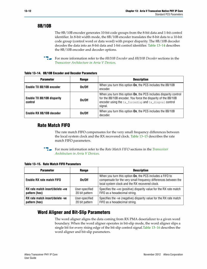
13–12 Chapter 13: Arria V Transceiver Native PHY IP CoreStandard PCS Parameters
8B/10BThe 8B/10B encoder generates 10-bit code groups from the 8-bit data and 1-bit control identifier. In 8-bit width mode, the 8B/10B encoder translates the 8-bit data to a 10-bit code group (control word or data word) with proper disparity. The 8B/10B decoder decodes the data into an 8-bit data and 1-bit control identifier. Table 13–14 describes the 8B/10B encoder and decoder options.
f For more information refer to the 8B/10B Encoder and 8B/10B Decoder sections in the Transceiver Architecture in Arria V Devices.
Rate Match FIFOThe rate match FIFO compensates for the very small frequency differences between the local system clock and the RX recovered clock. Table 13–15 describes the rate match FIFO parameters.
f For more information refer to the Rate Match FIFO sections in the Transceiver Architecture in Arria V Devices.
Word Aligner and Bit-Slip ParametersThe word aligner aligns the data coming from RX PMA deserializer to a given word boundary. When the word aligner operates in bit-slip mode, the word aligner slips a single bit for every rising edge of the bit slip control signal.Table 13–16 describes the word aligner and bit-slip parameters.
Table 13–14. 8B/10B Encoder and Decoder Parameters
Parameter Range Description
Enable TX 8B/10B encoder On/Off When you turn this option On, the PCS includes the 8B/10B encoder.
Enable TX 8B/10B disparity control On/Off
When you turn this option On, the PCS includes disparity control for the 8B/10B encoder. You force the disparity of the 8B/10B encoder using the tx_forcedisp and tx_dispval control signal.
Enable RX 8B/10B decoder On/Off When you turn this option On, the PCS includes the 8B/10B decoder.
Table 13–15. Rate Match FIFO Parameters
Parameter Range Description
Enable RX rate match FIFO On/OffWhen you turn this option On, the PCS includes a FIFO to compensate for the very small frequency differences between the local system clock and the RX recovered clock.
RX rate match insert/delete +ve pattern (hex)
User-specified 20 bit pattern
Specifies the +ve (positive) disparity value for the RX rate match FIFO as a hexadecimal string.
RX rate match insert/delete -ve pattern (hex)
User-specified 20 bit pattern
Specifies the -ve (negative) disparity value for the RX rate match FIFO as a hexadecimal string.
Altera Transceiver PHY IP Core November 2012 Altera CorporationUser Guide
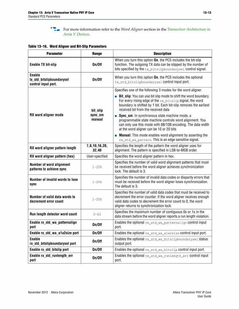
Chapter 13: Arria V Transceiver Native PHY IP Core 13–13Standard PCS Parameters
f For more information refer to the Word Aligner section in the Transceiver Architecture in Arria V Devices.
Table 13–16. Word Aligner and Bit-Slip Parameters
Parameter Range Description
Enable TX bit-slip On/OffWhen you turn this option On, the PCS includes the bit-slip function. The outgoing TX data can be slipped by the number of bits specified by the tx_bitslipboundarysel control signal.
Enable tx_std_bitslipboundarysel control input port.
On/Off When you turn this option On, the PCS includes the optional tx_std_bitslipboundarysel control input port.
RX word aligner modebit_slipsync_smmanual
Specifies one of the following 3 modes for the word aligner:
■ Bit_slip: You can use bit slip mode to shift the word boundary. For every rising edge of the rx_bitslip signal, the word boundary is shifted by 1 bit. Each bit-slip removes the earliest received bit from the received data
■ Sync_sm: In synchronous state machine mode, a programmable state machine controls word alignment. You can only use this mode with 8B/10B encoding. The data width at the word aligner can be 10 or 20 bits
■ Manual: This mode enables word alignment by asserting the rx_std_wa_pattern. This is an edge sensitive signal.
RX word aligner pattern length 7,8,10,16,20,32,40
Specifies the length of the pattern the word aligner uses for alignment. The pattern is specified in LSB-to-MSB order.
RX word aligner pattern (hex) User-specified Specifies the word aligner pattern in hex.
Number of word alignment patterns to achieve sync 1–256
Specifies the number of valid word alignment patterns that must be received before the word aligner achieves synchronization lock. The default is 3.
Number of invalid words to lose sync 1–256
Specifies the number of invalid data codes or disparity errors that must be received before the word aligner loses synchronization. The default is 3.
Number of valid data words to decrement error count 1–256
Specifies the number of valid data codes that must be received to decrement the error counter. If the word aligner receives enough valid data codes to decrement the error count to 0, the word aligner returns to synchronization lock.
Run length detector word count 0–63Specifies the maximum number of contiguous 0s or 1s in the data stream before the word aligner reports a run length violation.
Enable rx_std_wa_patternalign port On/Off Enables the optional rx_std_wa_patternalign control input
port.
Enable rx_std_wa_a1a2size port On/Off Enables the optional rx_std_wa_a1a2size control input port.
Enable rx_std_bitslipboundarysel port On/Off Enables the optional rx_std_wa_bitslipboundarysel status
output port.
Enable rx_std_bitslip port On/Off Enables the optional rx_std_wa_bitslip control input port.
Enable rx_std_runlength_err port On/Off Enables the optional rx_std_wa_runlength_err control input
port.
November 2012 Altera Corporation Altera Transceiver PHY IP CoreUser Guide
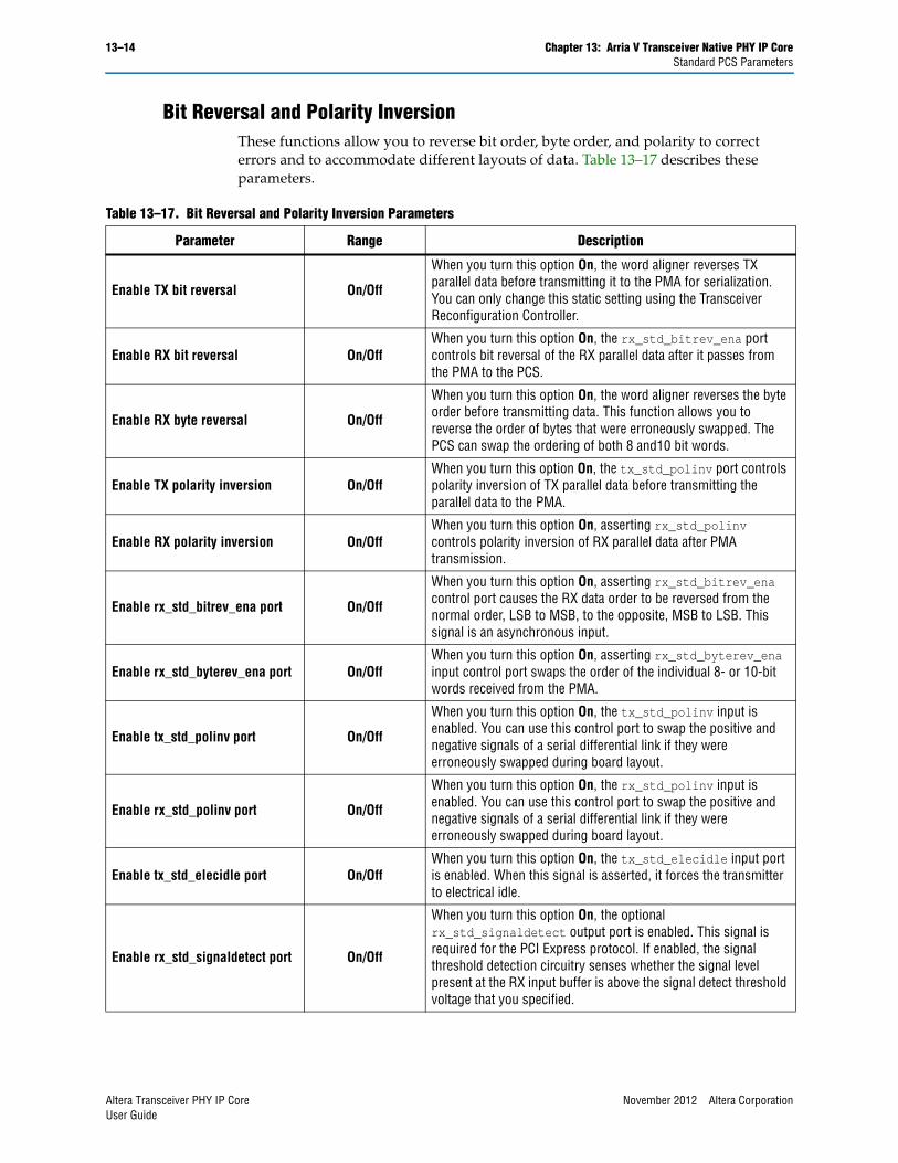
13–14 Chapter 13: Arria V Transceiver Native PHY IP CoreStandard PCS Parameters
Bit Reversal and Polarity InversionThese functions allow you to reverse bit order, byte order, and polarity to correct errors and to accommodate different layouts of data. Table 13–17 describes these parameters.
Table 13–17. Bit Reversal and Polarity Inversion Parameters
Parameter Range Description
Enable TX bit reversal On/Off
When you turn this option On, the word aligner reverses TX parallel data before transmitting it to the PMA for serialization. You can only change this static setting using the Transceiver Reconfiguration Controller.
Enable RX bit reversal On/OffWhen you turn this option On, the rx_std_bitrev_ena port controls bit reversal of the RX parallel data after it passes from the PMA to the PCS.
Enable RX byte reversal On/Off
When you turn this option On, the word aligner reverses the byte order before transmitting data. This function allows you to reverse the order of bytes that were erroneously swapped. The PCS can swap the ordering of both 8 and10 bit words.
Enable TX polarity inversion On/OffWhen you turn this option On, the tx_std_polinv port controls polarity inversion of TX parallel data before transmitting the parallel data to the PMA.
Enable RX polarity inversion On/OffWhen you turn this option On, asserting rx_std_polinv controls polarity inversion of RX parallel data after PMA transmission.
Enable rx_std_bitrev_ena port On/Off
When you turn this option On, asserting rx_std_bitrev_ena control port causes the RX data order to be reversed from the normal order, LSB to MSB, to the opposite, MSB to LSB. This signal is an asynchronous input.
Enable rx_std_byterev_ena port On/OffWhen you turn this option On, asserting rx_std_byterev_ena input control port swaps the order of the individual 8- or 10-bit words received from the PMA.
Enable tx_std_polinv port On/Off
When you turn this option On, the tx_std_polinv input is enabled. You can use this control port to swap the positive and negative signals of a serial differential link if they were erroneously swapped during board layout.
Enable rx_std_polinv port On/Off
When you turn this option On, the rx_std_polinv input is enabled. You can use this control port to swap the positive and negative signals of a serial differential link if they were erroneously swapped during board layout.
Enable tx_std_elecidle port On/OffWhen you turn this option On, the tx_std_elecidle input port is enabled. When this signal is asserted, it forces the transmitter to electrical idle.
Enable rx_std_signaldetect port On/Off
When you turn this option On, the optional rx_std_signaldetect output port is enabled. This signal is required for the PCI Express protocol. If enabled, the signal threshold detection circuitry senses whether the signal level present at the RX input buffer is above the signal detect threshold voltage that you specified.
Altera Transceiver PHY IP Core November 2012 Altera CorporationUser Guide
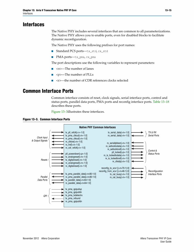
Chapter 13: Arria V Transceiver Native PHY IP Core 13–15Interfaces
InterfacesThe Native PHY includes several interfaces that are common to all parameterizations. The Native PHY allows you to enable ports, even for disabled blocks to facilitate dynamic reconfiguration.
The Native PHY uses the following prefixes for port names:
■ Standard PCS ports—tx_std, rx_std
■ PMA ports—tx_pma, rx_pma
The port descriptions use the following variables to represent parameters:
■ <n>—The number of lanes
■ <p>—The number of PLLs
■ <r>—the number of CDR references clocks selected
Common Interface PortsCommon interface consists of reset, clock signals, serial interface ports, control and status ports, parallel data ports, PMA ports and reconfig interface ports. Table 13–18 describes these ports.
Figure 13–3illustrates these interfaces.
Figure 13–3. Common Interface Ports
tx_pll_refclk[<r>-1:0]tx_pma_clkout[<n>-1:0]rx_pma_clkout[<n>-1:0]rx_clklow[<n>-1:0]rx_fref[<n>-1:0]rx_cdr_refclk[<r>-1:0]
Clock Input& Output Signals
rx_seriallpbken[<n>-1:0]rx_setlocktodata[<n>-1:0]
rx_setlocktoref[<n>-1:0]pll_locked[<p>-1:0]
rx_is_lockedtodata[<n>-1:0]rx_is_lockedtoref[<n>-1:0]
rx_clkslip[<n>-1:0]
Control &Status Portspll_powerdown[<p>-1:0]
tx_analogreset[<n>-1:0]tx_digitalreset[<n>-1:0]rx_analogreset[<n>-1:0]rx_digitalreset[<n>-1:0]
Resets
QPI
tx_pma_parallel_data[<n>80-1:0]rx_pma_parallel_data[<n>80-1:0]tx_parallel_data[<n>64-1:0]rx_parallel_data[<n>64-1:0]
tx_pma_qpipulluptx_pma_qpipulldntx_pma_txdetectrxtx_pma_rxfoundrx_pma_qpipulldn
ParallelData Ports
tx_serial_data[<n>-1:0]rx_serial_data[<n>-1:0]
TX & RXSerial Ports
reconfig_to_xcvr [(<n>70-1):0]reconfig_from_xcvr [(<n>46-1):0]
tx_cal_busy[<n>-1:0]rx_cal_busy[<n>-1:0]
ReconfigurationInterface Ports
Native PHY Common Interfaces
November 2012 Altera Corporation Altera Transceiver PHY IP CoreUser Guide
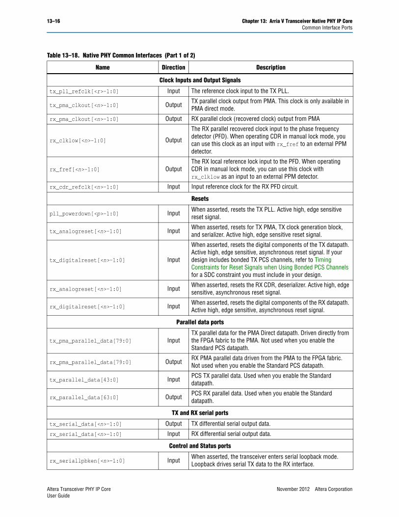
13–16 Chapter 13: Arria V Transceiver Native PHY IP CoreCommon Interface Ports
Table 13–18. Native PHY Common Interfaces (Part 1 of 2)
Name Direction Description
Clock Inputs and Output Signals
tx_pll_refclk[<r>-1:0] Input The reference clock input to the TX PLL.
tx_pma_clkout[<n>-1:0] Output TX parallel clock output from PMA. This clock is only available in PMA direct mode.
rx_pma_clkout[<n>-1:0] Output RX parallel clock (recovered clock) output from PMA
rx_clklow[<n>-1:0] Output
The RX parallel recovered clock input to the phase frequency detector (PFD). When operating CDR in manual lock mode, you can use this clock as an input with rx_fref to an external PPM detector.
rx_fref[<n>-1:0] OutputThe RX local reference lock input to the PFD. When operating CDR in manual lock mode, you can use this clock with rx_clklow as an input to an external PPM detector.
rx_cdr_refclk[<n>-1:0] Input Input reference clock for the RX PFD circuit.
Resets
pll_powerdown[<p>-1:0] Input When asserted, resets the TX PLL. Active high, edge sensitive reset signal.
tx_analogreset[<n>-1:0] Input When asserted, resets for TX PMA, TX clock generation block, and serializer. Active high, edge sensitive reset signal.
tx_digitalreset[<n>-1:0] Input
When asserted, resets the digital components of the TX datapath. Active high, edge sensitive, asynchronous reset signal. If your design includes bonded TX PCS channels, refer to Timing Constraints for Reset Signals when Using Bonded PCS Channels for a SDC constraint you must include in your design.
rx_analogreset[<n>-1:0] Input When asserted, resets the RX CDR, deserializer. Active high, edge sensitive, asynchronous reset signal.
rx_digitalreset[<n>-1:0] Input When asserted, resets the digital components of the RX datapath. Active high, edge sensitive, asynchronous reset signal.
Parallel data ports
tx_pma_parallel_data[79:0] InputTX parallel data for the PMA Direct datapath. Driven directly from the FPGA fabric to the PMA. Not used when you enable the Standard PCS datapath.
rx_pma_parallel_data[79:0] Output RX PMA parallel data driven from the PMA to the FPGA fabric. Not used when you enable the Standard PCS datapath.
tx_parallel_data[43:0] Input PCS TX parallel data. Used when you enable the Standard datapath.
rx_parallel_data[63:0] Output PCS RX parallel data. Used when you enable the Standard datapath.
TX and RX serial ports
tx_serial_data[<n>-1:0] Output TX differential serial output data.
rx_serial_data[<n>-1:0] Input RX differential serial output data.
Control and Status ports
rx_seriallpbken[<n>-1:0] Input When asserted, the transceiver enters serial loopback mode. Loopback drives serial TX data to the RX interface.
Altera Transceiver PHY IP Core November 2012 Altera CorporationUser Guide
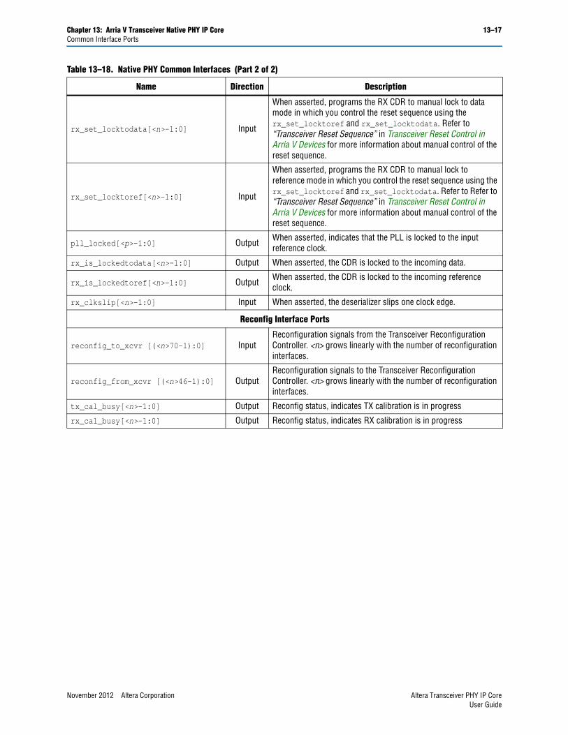
Chapter 13: Arria V Transceiver Native PHY IP Core 13–17Common Interface Ports
rx_set_locktodata[<n>-1:0] Input
When asserted, programs the RX CDR to manual lock to data mode in which you control the reset sequence using the rx_set_locktoref and rx_set_locktodata. Refer to “Transceiver Reset Sequence” in Transceiver Reset Control in Arria V Devices for more information about manual control of the reset sequence.
rx_set_locktoref[<n>-1:0] Input
When asserted, programs the RX CDR to manual lock to reference mode in which you control the reset sequence using the rx_set_locktoref and rx_set_locktodata. Refer to Refer to “Transceiver Reset Sequence” in Transceiver Reset Control in Arria V Devices for more information about manual control of the reset sequence.
pll_locked[<p>-1:0] Output When asserted, indicates that the PLL is locked to the input reference clock.
rx_is_lockedtodata[<n>-1:0] Output When asserted, the CDR is locked to the incoming data.
rx_is_lockedtoref[<n>-1:0] Output When asserted, the CDR is locked to the incoming reference clock.
rx_clkslip[<n>-1:0] Input When asserted, the deserializer slips one clock edge.
Reconfig Interface Ports
reconfig_to_xcvr [(<n>70-1):0] InputReconfiguration signals from the Transceiver Reconfiguration Controller. <n> grows linearly with the number of reconfiguration interfaces.
reconfig_from_xcvr [(<n>46-1):0] OutputReconfiguration signals to the Transceiver Reconfiguration Controller. <n> grows linearly with the number of reconfiguration interfaces.
tx_cal_busy[<n>-1:0] Output Reconfig status, indicates TX calibration is in progress
rx_cal_busy[<n>-1:0] Output Reconfig status, indicates RX calibration is in progress
Table 13–18. Native PHY Common Interfaces (Part 2 of 2)
Name Direction Description
November 2012 Altera Corporation Altera Transceiver PHY IP CoreUser Guide
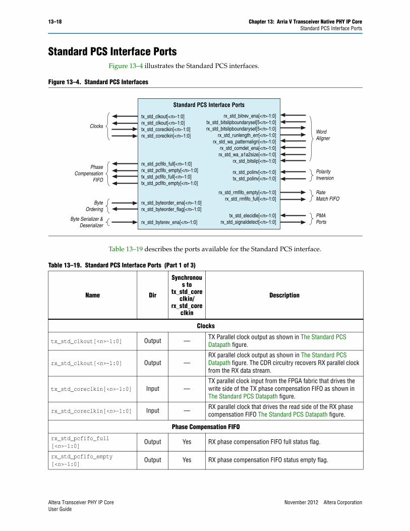
13–18 Chapter 13: Arria V Transceiver Native PHY IP CoreStandard PCS Interface Ports
Standard PCS Interface PortsFigure 13–4 illustrates the Standard PCS interfaces.
Table 13–19 describes the ports available for the Standard PCS interface.
Figure 13–4. Standard PCS Interfaces
tx_std_clkout[<n>-1:0] rx_std_clkout[<n>-1:0]tx_std_coreclkin[<n>-1:0]rx_std_coreclkin[<n>-1:0]
ClocksWordAligner
rx_std_pcfifo_full[<n>-1:0] rx_std_pcfifo_empty[<n>-1:0] tx_std_pcfifo_full[<n>-1:0] tx_std_pcfifo_empty[<n>-1:0]
PhaseCompensation
FIFO
rx_std_byteorder_ena[<n>-1:0] rx_std_byteorder_flag[<n>-1:0]
ByteOrdering
rx_std_rmfifo_empty[<n>-1:0]rx_std_rmfifo_full[<n>-1:0]
RateMatch FIFO
rx_std_polinv[<n>-1:0]tx_std_polinv[<n>-1:0]
PolarityInversion
PMAPorts
Standard PCS Interface Ports
rx_std_bitrev_ena[<n>-1:0]tx_std_bitslipboundarysel[5<n>-1:0]rx_std_bitslipboundarysel[5<n>-1:0]
rx_std_runlength_err[<n>-1:0]rx_std_wa_patternalign[<n>-1:0]
rx_std_comdet_ena[<n>-1:0]rx_std_wa_a1a2size[<n>-1:0]
rx_std_bitslip[<n>-1:0]
tx_std_elecidle[<n>-1:0]rx_std_signaldetect[<n>-1:0]rx_std_byterev_ena[<n>-1:0]
Byte Serializer &Deserializer
Table 13–19. Standard PCS Interface Ports (Part 1 of 3)
Name Dir
Synchronous to
tx_std_coreclkin/
rx_std_coreclkin
Description
Clocks
tx_std_clkout[<n>-1:0] Output — TX Parallel clock output as shown in The Standard PCS Datapath figure.
rx_std_clkout[<n>-1:0] Output —RX parallel clock output as shown in The Standard PCS Datapath figure. The CDR circuitry recovers RX parallel clock from the RX data stream.
tx_std_coreclkin[<n>-1:0] Input —TX parallel clock input from the FPGA fabric that drives the write side of the TX phase compensation FIFO as shown in The Standard PCS Datapath figure.
rx_std_coreclkin[<n>-1:0] Input — RX parallel clock that drives the read side of the RX phase compensation FIFO The Standard PCS Datapath figure.
Phase Compensation FIFO
rx_std_pcfifo_full[<n>-1:0]
Output Yes RX phase compensation FIFO full status flag.
rx_std_pcfifo_empty[<n>-1:0]
Output Yes RX phase compensation FIFO status empty flag.
Altera Transceiver PHY IP Core November 2012 Altera CorporationUser Guide
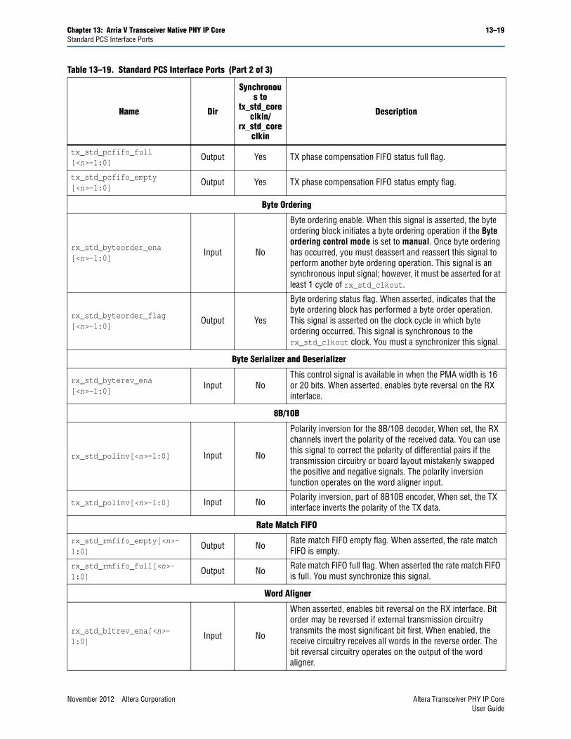
Chapter 13: Arria V Transceiver Native PHY IP Core 13–19Standard PCS Interface Ports
tx_std_pcfifo_full[<n>-1:0]
Output Yes TX phase compensation FIFO status full flag.
tx_std_pcfifo_empty[<n>-1:0]
Output Yes TX phase compensation FIFO status empty flag.
Byte Ordering
rx_std_byteorder_ena[<n>-1:0]
Input No
Byte ordering enable. When this signal is asserted, the byte ordering block initiates a byte ordering operation if the Byte ordering control mode is set to manual. Once byte ordering has occurred, you must deassert and reassert this signal to perform another byte ordering operation. This signal is an synchronous input signal; however, it must be asserted for at least 1 cycle of rx_std_clkout.
rx_std_byteorder_flag[<n>-1:0]
Output Yes
Byte ordering status flag. When asserted, indicates that the byte ordering block has performed a byte order operation. This signal is asserted on the clock cycle in which byte ordering occurred. This signal is synchronous to the rx_std_clkout clock. You must a synchronizer this signal.
Byte Serializer and Deserializer
rx_std_byterev_ena[<n>-1:0]
Input NoThis control signal is available in when the PMA width is 16 or 20 bits. When asserted, enables byte reversal on the RX interface.
8B/10B
rx_std_polinv[<n>-1:0] Input No
Polarity inversion for the 8B/10B decoder, When set, the RX channels invert the polarity of the received data. You can use this signal to correct the polarity of differential pairs if the transmission circuitry or board layout mistakenly swapped the positive and negative signals. The polarity inversion function operates on the word aligner input.
tx_std_polinv[<n>-1:0] Input No Polarity inversion, part of 8B10B encoder, When set, the TX interface inverts the polarity of the TX data.
Rate Match FIFO
rx_std_rmfifo_empty[<n>-1:0]
Output No Rate match FIFO empty flag. When asserted, the rate match FIFO is empty.
rx_std_rmfifo_full[<n>-1:0]
Output No Rate match FIFO full flag. When asserted the rate match FIFO is full. You must synchronize this signal.
Word Aligner
rx_std_bitrev_ena[<n>-1:0]
Input No
When asserted, enables bit reversal on the RX interface. Bit order may be reversed if external transmission circuitry transmits the most significant bit first. When enabled, the receive circuitry receives all words in the reverse order. The bit reversal circuitry operates on the output of the word aligner.
Table 13–19. Standard PCS Interface Ports (Part 2 of 3)
Name Dir
Synchronous to
tx_std_coreclkin/
rx_std_coreclkin
Description
November 2012 Altera Corporation Altera Transceiver PHY IP CoreUser Guide
13–20 Chapter 13: Arria V Transceiver Native PHY IP CoreSDC Timing Constraints
SDC Timing Constraints The Quartus II 12.1 software reports timing violations for asynchronous inputs to the Standard PCS and 10G PCS. Because many violations are for asynchronous paths, they do not represent actual timing failures. You may choose one of the following three approaches to identify these false timing paths to the Quartus II or TimeQuest software.
tx_std_bitslipboundarysel[5<n>-1:0]
Input No Bit-Slip boundary selection signal. Specifies the number of bits that the TX bit slipper must slip.
rx_std_bitslipboundarysel[5<n>-1:0]
Output NoThis signal operates when the word aligner is in bit-slip word alignment mode. It reports the number of bits that the RX block slipped to achieve deterministic latency.
rx_std_runlength_err[<n>-1:0]
Output NoWhen asserted, indicates a run length violation. Asserted if the number of consecutive 1s or 0s exceeds the number specified in the parameter editor GUI.
rx_st_wa_patternalign Input No
Active when you place the word aligner in manual mode. In manual mode, you align words by asserting rx_st_wa_patternalign. rx_st_wa_patternalign is edge sensitive.
For more information refer to the Word Aligner section in the Transceiver Architecture in Arria V Devices.
rx_std_wa_a1a2size[<n>-1:0]
Input No
Used for the SONET protocol. Assert when the A1 and A2 framing bytes must be detected. A1 and A2 are SONET backplane bytes and are only used when the PMA data width is 8 bits.
rx_std_bitslip[<n>-1:0] Input No
Used when word aligner mode is bit-slip mode. For every rising edge of the rx_std_bitslip signal, the word boundary is shifted by 1 bit. Each bitslip removes the earliest received bit from the received data. You must synchronize this signal.
Miscellaneous
tx_std_elecidle[<n>-1:0] Input
When asserted, enables a circuit to detect a downstream receiver. This signal must be driven low when not in use because it causes the TX PMA to enter electrical idle mode with the TX serial data signals in tri-state mode.
rx_std_signaldetect[<n>-1:0]
Output No
Signal threshold detect indicator. When asserted, it indicates that the signal present at the receiver input buffer is above the programmed signal detection threshold value. You must synchronize this signal.
Table 13–19. Standard PCS Interface Ports (Part 3 of 3)
Name Dir
Synchronous to
tx_std_coreclkin/
rx_std_coreclkin
Description
Altera Transceiver PHY IP Core November 2012 Altera CorporationUser Guide
Chapter 13: Arria V Transceiver Native PHY IP Core 13–21SDC Timing Constraints
■ You can cut these paths in your Synopsys Design Constraints (.sdc) file by using the set_false_path command as shown in Example 13–1.
■ You can use the set_max_delay constraint on a given path to create a constraint for asynchronous signals that do not have a specific clock relationship but require a maximum path delay. Figure 13–2 illustrates this approach.
■ You can use the set_false path command only during Timequest timing analysis. Example 13–3 illustrates this approach.
1 In in all of these examples, you must substitute you actual signal names for the signal names shown.
Example 13–1. Using the set_false_path Constraint to Identify Asynchronous Inputs
set_false_path -through {*10gtxbursten*} -to [get_registers *10g_tx_pcs*SYNC_DATA_REG*]set_false_path -through {*10gtxdiagstatus*} -to [get_registers *10g_tx_pcs*SYNC_DATA_REG*]set_false_path -through {*10gtxwordslip*} -to [get_registers *10g_tx_pcs*SYNC_DATA_REG*]set_false_path -through {*10gtxbitslip*} -to [get_registers *10g_tx_pcs*SYNC_DATA_REG*]set_false_path -through {*10grxbitslip*} -to [get_registers *10g_rx_pcs*SYNC_DATA_REG*]set_false_path -through {*10grxclrbercount*} -to [get_registers *10g_rx_pcs*SYNC_DATA_REG*] set_false_path -through {*10grxclrerrblkcnt*} -to [get_registers *10g_rx_pcs*SYNC_DATA_REG*] set_false_path -through {*10grxprbserrclr*} -to [get_registers *10g_rx_pcs*SYNC_DATA_REG*]
set_false_path -through {*8gbitslip*} -to [get_registers *8g_rx_pcs*SYNC_DATA_REG*]set_false_path -through {*8gbytordpld*} -to [get_registers *8g_rx_pcs*SYNC_DATA_REG*] set_false_path -through {*8gcmpfifoburst*} -to [get_registers *8g_rx_pcs*SYNC_DATA_REG*] set_false_path -through {*8gphfifoburstrx*} -to [get_registers *8g_rx_pcs*SYNC_DATA_REG*]
set_false_path -through {*8gsyncsmen*} -to [get_registers *8g*pcs*SYNC_DATA_REG*]set_false_path -through {*8gwrdisablerx*} -to [get_registers *8g_rx_pcs*SYNC_DATA_REG*] set_false_path -through {*rxpolarity*} -to [get_registers *SYNC_DATA_REG*]set_false_path -through {*pldeidleinfersel*} -to [get_registers *SYNC_DATA_REG*]
Example 13–2. Using the max_delay Constraint to Identify Asynchronous Inputs
# Example: Apply 10ns max delayset_max_delay -from *tx_from_fifo* -to *8g*pcs*SYNC_DATA_REG1 10
Example 13–3. Using the set_false TimeQuest Constraint to Identify Asynchronous Inputs
#if {$::TimeQuestInfo(nameofexecutable) eq "quartus_fit"} { #} else {#set_false_path -from [get_registers {*tx_from_fifo*}] -through {*txbursten*} -to [get_registers *8g_*_pcs*SYNC_DATA_REG
November 2012 Altera Corporation Altera Transceiver PHY IP CoreUser Guide
13–22 Chapter 13: Arria V Transceiver Native PHY IP CoreDynamic Reconfiguration
Dynamic Reconfiguration As silicon progresses towards smaller process nodes, circuit performance is affected more by variations due to process, voltage, and temperature (PVT). These process variations result in analog voltages that can be offset from required ranges. The calibration performed by the dynamic reconfiguration interface compensates for variations due to PVT.
For non-bonded clocks, each channel and each TX PLL has a separate dynamic reconfiguration interfaces. The MegaWizard Plug-In Manager provides informational messages on the connectivity of these interfaces. Example 13–4 shows the messages for the Arria V Native PHY with four duplex channels, four TX PLLs, in a non-bonded configuration.
For more information about transceiver reconfiguration refer to Transceiver Reconfiguration Controller IP Core.
Simulation SupportThe Quartus II 12.1 release provides simulation and compilation support for the Arria V Native PHY IP Core. Refer to Running a Simulation Testbench for a description of the directories and files that the Quartus II software creates automatically when you generate your Arria V Transceiver Native PHY IP Core.
Example 13–4. Informational Messages for the Transceiver Reconfiguration Interface
PHY IP will require 8 reconfiguration interfaces for connection to the external reconfiguration controller.Reconfiguration interface offsets 0-3 are connected to the transceiver channels.Reconfiguration interface offsets 4–7 are connected to the transmit PLLs.
Altera Transceiver PHY IP Core November 2012 Altera CorporationUser Guide
November 2012 Altera Corporation
14. Arria V GZ Transceiver Native PHY IPCore
The Arria V GZTransceiver Native PHY IP Core provides direct access to all control and status signals of the transceiver channels. Unlike other PHY IP Cores, the Native PHY IP Core does not include an Avalon Memory-Mapped (Avalon-MM) interface. Instead, it exposes all signals directly as ports. The Arria V GZ Transceiver Native PHY IP Core provides the following three datapaths:
■ Standard PCS
■ 10G PCS
■ PMA Direct
You can enable the Standard PCS, the 10G PCS, or both if your design uses the Transceiver Reconfiguration Controller to change dynamically between the two PCS datapaths. The transceiver PHY does not include an embedded reset controller. You can either design custom reset logic or incorporate Altera’s “Transceiver PHY Reset Controller IP Core” to implement reset functionality. The Native Transceiver PHY’s primary use in Arria V GT devices for data rates greater than 6.5536 Gbps.
In PMA Direct mode, the Native PHY provides direct access to the PMA from the FPGA fabric; consequently, the latency for transmitted and received data is very low. However, you must implement any PCS function that your design requires in the FPGA fabric.
Altera Transceiver PHY IP CoreUser Guide
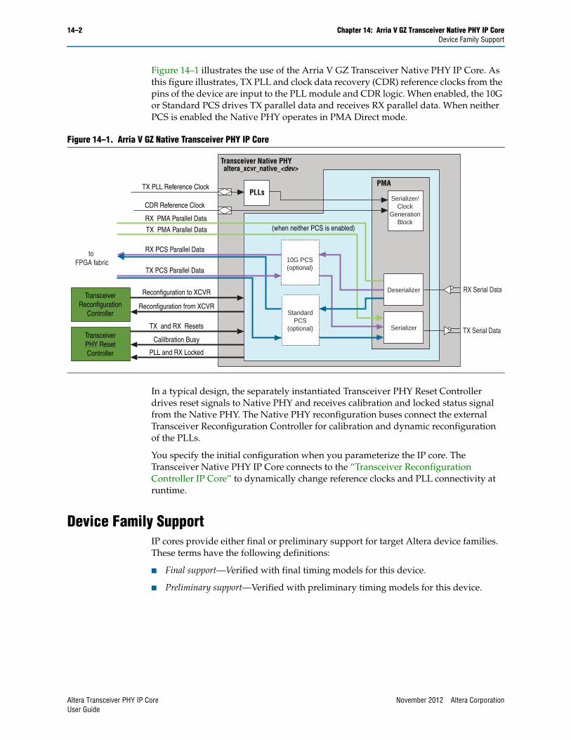
14–2 Chapter 14: Arria V GZ Transceiver Native PHY IP CoreDevice Family Support
Figure 14–1 illustrates the use of the Arria V GZ Transceiver Native PHY IP Core. As this figure illustrates, TX PLL and clock data recovery (CDR) reference clocks from the pins of the device are input to the PLL module and CDR logic. When enabled, the 10G or Standard PCS drives TX parallel data and receives RX parallel data. When neither PCS is enabled the Native PHY operates in PMA Direct mode.
In a typical design, the separately instantiated Transceiver PHY Reset Controller drives reset signals to Native PHY and receives calibration and locked status signal from the Native PHY. The Native PHY reconfiguration buses connect the external Transceiver Reconfiguration Controller for calibration and dynamic reconfiguration of the PLLs.
You specify the initial configuration when you parameterize the IP core. The Transceiver Native PHY IP Core connects to the “Transceiver Reconfiguration Controller IP Core” to dynamically change reference clocks and PLL connectivity at runtime.
Device Family SupportIP cores provide either final or preliminary support for target Altera device families. These terms have the following definitions:
■ Final support—Verified with final timing models for this device.
■ Preliminary support—Verified with preliminary timing models for this device.
Figure 14–1. Arria V GZ Native Transceiver PHY IP Core
PLLsPMA
altera_xcvr_native_<dev>Transceiver Native PHY
TransceiverReconfiguration
Controller
Reconfiguration to XCVR
Reconfiguration from XCVR
TX and RX Resets
Calilbration Busy
PLL and RX Locked
RX PCS Parallel Data
TX PCS Parallel Data
CDR Reference Clock
(when neither PCS is enabled)
TX PLL Reference Clock
Serializer/Clock
GenerationBlock
RX Serial Data
to FPGA fabric
TransceiverPHY ResetController
TX PMA Parallel Data
RX PMA Parallel Data
TX Serial DataSerializer
Deserializer
StandardPCS
(optional)
10G PCS(optional)
Altera Transceiver PHY IP Core November 2012 Altera CorporationUser Guide
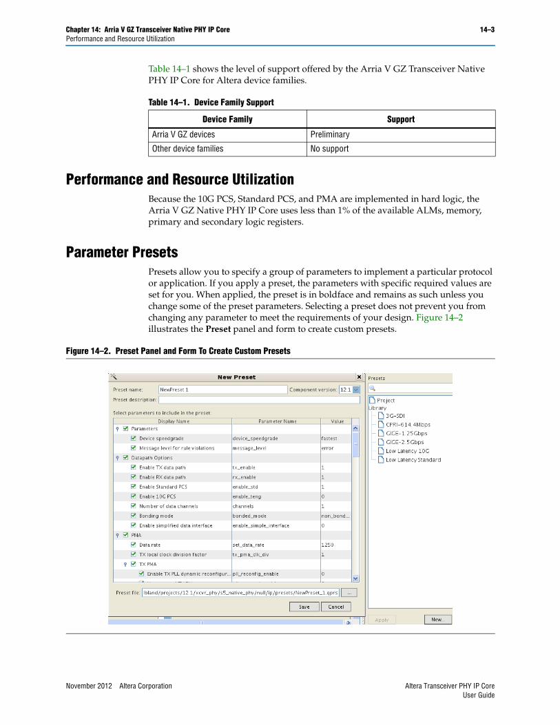
Chapter 14: Arria V GZ Transceiver Native PHY IP Core 14–3Performance and Resource Utilization
Table 14–1 shows the level of support offered by the Arria V GZ Transceiver Native PHY IP Core for Altera device families.
Performance and Resource UtilizationBecause the 10G PCS, Standard PCS, and PMA are implemented in hard logic, the Arria V GZ Native PHY IP Core uses less than 1% of the available ALMs, memory, primary and secondary logic registers.
Parameter PresetsPresets allow you to specify a group of parameters to implement a particular protocol or application. If you apply a preset, the parameters with specific required values are set for you. When applied, the preset is in boldface and remains as such unless you change some of the preset parameters. Selecting a preset does not prevent you from changing any parameter to meet the requirements of your design. Figure 14–2 illustrates the Preset panel and form to create custom presets.
Table 14–1. Device Family Support
Device Family Support
Arria V GZ devices Preliminary
Other device families No support
Figure 14–2. Preset Panel and Form To Create Custom Presets
November 2012 Altera Corporation Altera Transceiver PHY IP CoreUser Guide
14–4 Chapter 14: Arria V GZ Transceiver Native PHY IP CoreParameterizing the Arria V GZ Native PHY
Parameterizing the Arria V GZ Native PHYComplete the following steps to configure the Arria V GZ Native PHY IP Core in the MegaWizard Plug-In Manager:
1. For Which device family will you be using? select Arria V GZ from the list.
2. Click Installed Plug-Ins > Interfaces > Transceiver PHY > Arria V GZ Native PHY v12.1.
3. Use the tabs on the MegaWizard Plug-In Manager to select the options required for the protocol.
4. Click Finish to generate your customized Arria V GZ Native PHY IP Core.
General ParametersTable 14–2 lists the parameters available on the General Options tab. Note that you can enable the Standard PCS, the 10G PCS, or both if you intend to reconfigure between the two available PCS datapaths.
Table 14–2. General and Datapath Options (Part 1 of 2)
Name Range Description
Device speed grade fastest–3_H3 Specifies the speed grade.
Message level for rule violations errorwarning
When you select the error message level, the Quartus II rules checker reports an error if you specify incompatible parameters. If you select the warning message level, the Quartus II rules checker reports a warning instead of an error.
Datapath Options
Enable TX datapath On/Off When you turn this option On, the core includes the TX datapath.
Enable RX datapath On/Off When you turn this option On, the core includes the RX datapath.
Enable Standard PCS On/OffWhen you turn this option On, the core includes the Standard PCS. You can enable both the Standard and 10G PCS if you plan to dynamically reconfigure the Native PHY.
Enable 10G PCS On/OffWhen you turn this option On, the core includes the 10G PCS. You can enable both the Standard and 10G PCS if you plan to dynamically reconfigure the Native PHY.
Number of data channels Device Dependent Specifies the total number of data channels in each direction. From 1–32 channels are supported.
Altera Transceiver PHY IP Core November 2012 Altera CorporationUser Guide
Chapter 14: Arria V GZ Transceiver Native PHY IP Core 14–5PMA Parameters
PMA ParametersTable 14–3 describes the options available for the PMA.
f For more information about the PMA, refer to the PMA Architecture section in the Transceiver Architecture in Arria V Devices.Some parameters have ranges where the value is specified as Device Dependent. For such parameters, the possible range of frequencies and bandwidths depends on the device, speed grade, and other design characteristics. Refer to Device Datasheet for Arria V Devices for specific data for Arria V devices.
Bonding modeNon–bonded
×6fb_compensation
In Non–bonded mode, each channel is paired with a PLL. During Quartus II compilation, the Fitter merges all PLLs that meet merging requirements into a single PLL.
Select ×6 to use the same clock source for up to 6 channels in a single transceiver bank, resulting in reduced clock skew. You must use contiguous channels when you select ×6 bonding. In addition, you must place logical channel 0 in either physical channel 1 or 4. Physical channels 1 and 4 are indirect drivers of the ×6 clock network.
Select fb_compensation (feedback compensation) to use the same clock source for multiple channels across different transceiver banks to reduce clock skew.
Enable simplified data interface On/Off
When you turn this option On, the Native PHY presents only the relevant data bits. When you turn this option Off, the Native PHY presents the full raw interface to the fabric. If you plan to dynamically reconfigure the Native PHY, you must turn this option Off and you need to understand the mapping of data to the FPGA fabric. Refer to “Active Bits for Each Fabric Interface Width” for more information. When you turn this option On, the Native PHY presents an interface that includes only the data necessary for the single configuration specified.
Table 14–2. General and Datapath Options (Part 2 of 2)
Name Range Description
Table 14–3. PMA Options (Part 1 of 2)
Parameter Range Description
Data rate Device Dependent Specifies the data rate.
TX local clock division factor 1, 2, 4, 8Specifies the value of the divider available in the transceiver channels to divide the input clock to generate the correct frequencies for the parallel and serial clocks.
November 2012 Altera Corporation Altera Transceiver PHY IP CoreUser Guide
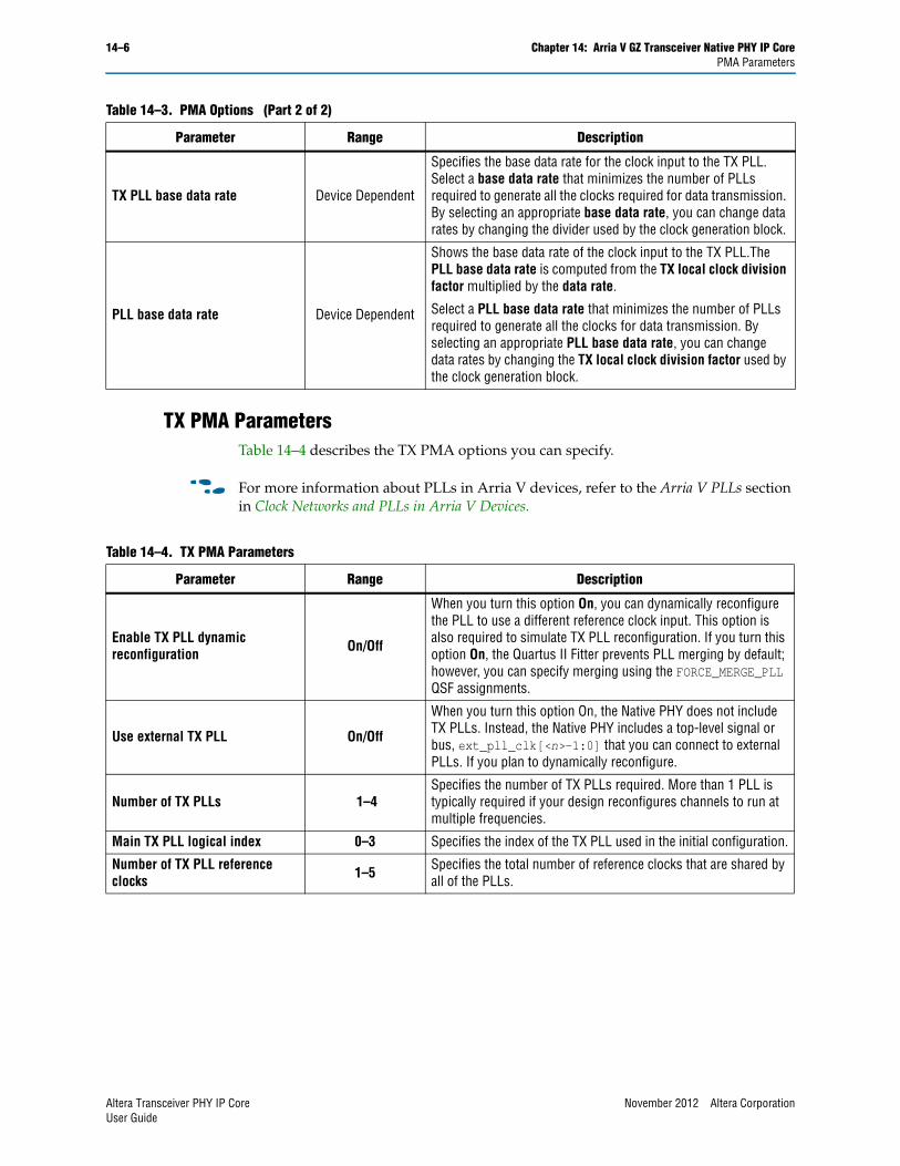
14–6 Chapter 14: Arria V GZ Transceiver Native PHY IP CorePMA Parameters
TX PMA ParametersTable 14–4 describes the TX PMA options you can specify.
f For more information about PLLs in Arria V devices, refer to the Arria V PLLs section in Clock Networks and PLLs in Arria V Devices.
TX PLL base data rate Device Dependent
Specifies the base data rate for the clock input to the TX PLL. Select a base data rate that minimizes the number of PLLs required to generate all the clocks required for data transmission. By selecting an appropriate base data rate, you can change data rates by changing the divider used by the clock generation block.
PLL base data rate Device Dependent
Shows the base data rate of the clock input to the TX PLL.The PLL base data rate is computed from the TX local clock division factor multiplied by the data rate.
Select a PLL base data rate that minimizes the number of PLLs required to generate all the clocks for data transmission. By selecting an appropriate PLL base data rate, you can change data rates by changing the TX local clock division factor used by the clock generation block.
Table 14–3. PMA Options (Part 2 of 2)
Parameter Range Description
Table 14–4. TX PMA Parameters
Parameter Range Description
Enable TX PLL dynamic reconfiguration On/Off
When you turn this option On, you can dynamically reconfigure the PLL to use a different reference clock input. This option is also required to simulate TX PLL reconfiguration. If you turn this option On, the Quartus II Fitter prevents PLL merging by default; however, you can specify merging using the FORCE_MERGE_PLL QSF assignments.
Use external TX PLL On/Off
When you turn this option On, the Native PHY does not include TX PLLs. Instead, the Native PHY includes a top-level signal or bus, ext_pll_clk[<n>-1:0] that you can connect to external PLLs. If you plan to dynamically reconfigure.
Number of TX PLLs 1–4Specifies the number of TX PLLs required. More than 1 PLL is typically required if your design reconfigures channels to run at multiple frequencies.
Main TX PLL logical index 0–3 Specifies the index of the TX PLL used in the initial configuration.
Number of TX PLL reference clocks 1–5 Specifies the total number of reference clocks that are shared by
all of the PLLs.
Altera Transceiver PHY IP Core November 2012 Altera CorporationUser Guide
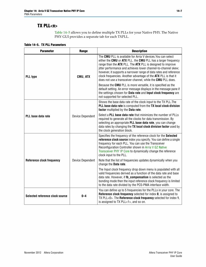
Chapter 14: Arria V GZ Transceiver Native PHY IP Core 14–7PMA Parameters
TX PLL<n>Table 14–5 allows you to define multiple TX PLLs for your Native PHY. The Native PHY GUI provides a separate tab for each TXPLL.
Table 14–5. TX PLL Parameters
Parameter Range Description
PLL type CMU, ATX
The CMU PLL is available for Arria V devices.You can select either the CMU or ATX PLL. the CMU PLL has a larger frequency range than the ATX PLL. The ATX PLL is designed to improve jitter performance and achieves lower channel-to-channel skew; however, it supports a narrower range of data rates and reference clock frequencies. Another advantage of the ATX PLL is that it does not use a transceiver channel, while the CMU PLL does.
Because the CMU PLL is more versatile, it is specified as the default setting. An error message displays in the message pane if the settings chosen for Data rate and Input clock frequency are not supported for selected PLL.
PLL base data rate Device Dependent
Shows the base data rate of the clock input to the TX PLL.The PLL base data rate is computed from the TX local clock division factor multiplied by the Data rate.
Select a PLL base data rate that minimizes the number of PLLs required to generate all the clocks for data transmission. By selecting an appropriate PLL base data rate, you can change data rates by changing the TX local clock division factor used by the clock generation block.
Reference clock frequency Device Dependent
Specifies the frequency of the reference clock for the Selected reference clock source index you specify. You can define a single frequency for each PLL. You can use the Transceiver Reconfiguration Controller shown in Arria V GZ Native Transceiver PHY IP Core to dynamically change the reference clock input to the PLL.
Note that the list of frequencies updates dynamically when you change the Data rate.
The Input clock frequency drop down menu is populated with all valid frequencies derived as a function of the data rate and base data rate. However, if fb_compensation is selected as the bonding mode then the input reference clock frequency is limited to the data rate divided by the PCS-PMA interface width.
Selected reference clock source 0–4
You can define up to 5 frequencies for the PLLs in your core. The Reference clock frequency selected for index 0, is assigned to TX PLL<0>. The Reference clock frequency selected for index 1, is assigned to TX PLL<1>, and so on.
November 2012 Altera Corporation Altera Transceiver PHY IP CoreUser Guide
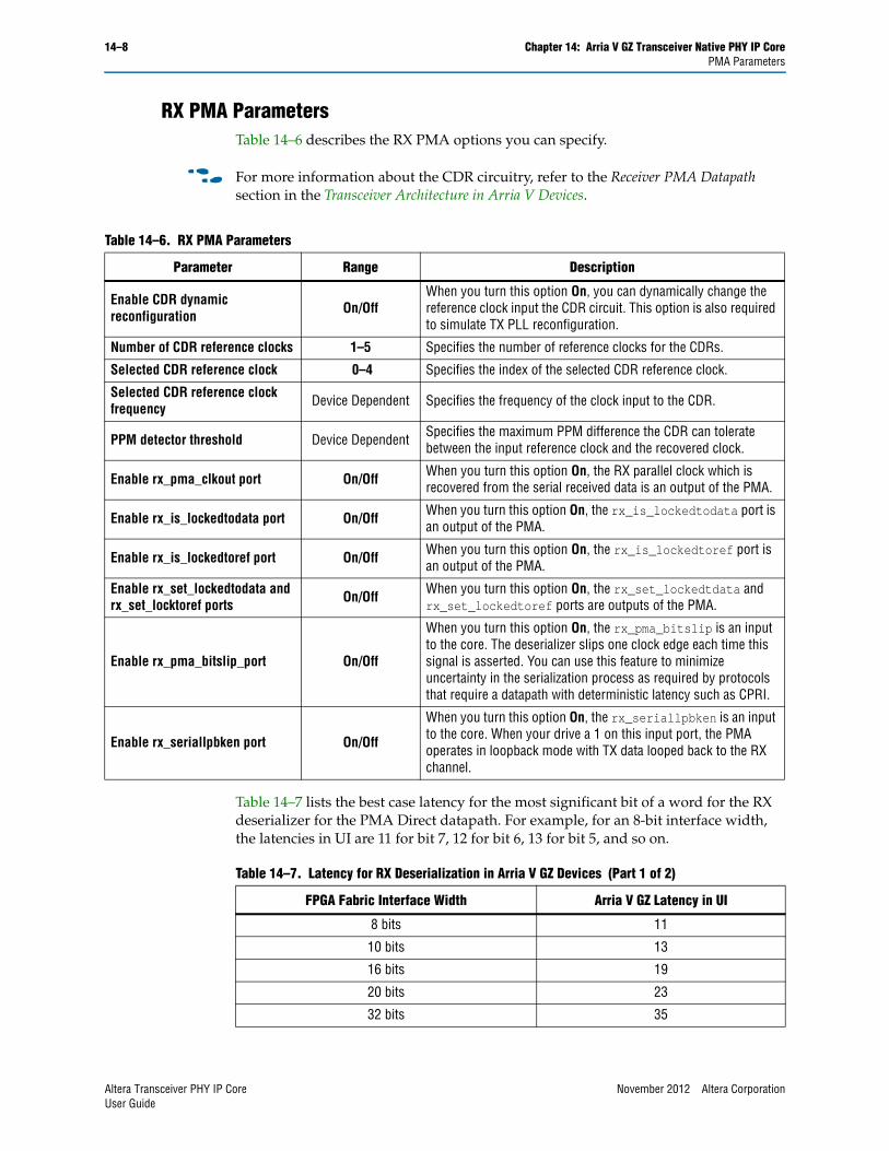
14–8 Chapter 14: Arria V GZ Transceiver Native PHY IP CorePMA Parameters
RX PMA ParametersTable 14–6 describes the RX PMA options you can specify.
f For more information about the CDR circuitry, refer to the Receiver PMA Datapath section in the Transceiver Architecture in Arria V Devices.
Table 14–7 lists the best case latency for the most significant bit of a word for the RX deserializer for the PMA Direct datapath. For example, for an 8-bit interface width, the latencies in UI are 11 for bit 7, 12 for bit 6, 13 for bit 5, and so on.
Table 14–6. RX PMA Parameters
Parameter Range Description
Enable CDR dynamic reconfiguration On/Off
When you turn this option On, you can dynamically change the reference clock input the CDR circuit. This option is also required to simulate TX PLL reconfiguration.
Number of CDR reference clocks 1–5 Specifies the number of reference clocks for the CDRs.
Selected CDR reference clock 0–4 Specifies the index of the selected CDR reference clock.
Selected CDR reference clock frequency Device Dependent Specifies the frequency of the clock input to the CDR.
PPM detector threshold Device Dependent Specifies the maximum PPM difference the CDR can tolerate between the input reference clock and the recovered clock.
Enable rx_pma_clkout port On/Off When you turn this option On, the RX parallel clock which is recovered from the serial received data is an output of the PMA.
Enable rx_is_lockedtodata port On/Off When you turn this option On, the rx_is_lockedtodata port is an output of the PMA.
Enable rx_is_lockedtoref port On/Off When you turn this option On, the rx_is_lockedtoref port is an output of the PMA.
Enable rx_set_lockedtodata and rx_set_locktoref ports On/Off When you turn this option On, the rx_set_lockedtdata and
rx_set_lockedtoref ports are outputs of the PMA.
Enable rx_pma_bitslip_port On/Off
When you turn this option On, the rx_pma_bitslip is an input to the core. The deserializer slips one clock edge each time this signal is asserted. You can use this feature to minimize uncertainty in the serialization process as required by protocols that require a datapath with deterministic latency such as CPRI.
Enable rx_seriallpbken port On/Off
When you turn this option On, the rx_seriallpbken is an input to the core. When your drive a 1 on this input port, the PMA operates in loopback mode with TX data looped back to the RX channel.
Table 14–7. Latency for RX Deserialization in Arria V GZ Devices (Part 1 of 2)
FPGA Fabric Interface Width Arria V GZ Latency in UI
8 bits 11
10 bits 13
16 bits 19
20 bits 23
32 bits 35
Altera Transceiver PHY IP Core November 2012 Altera CorporationUser Guide
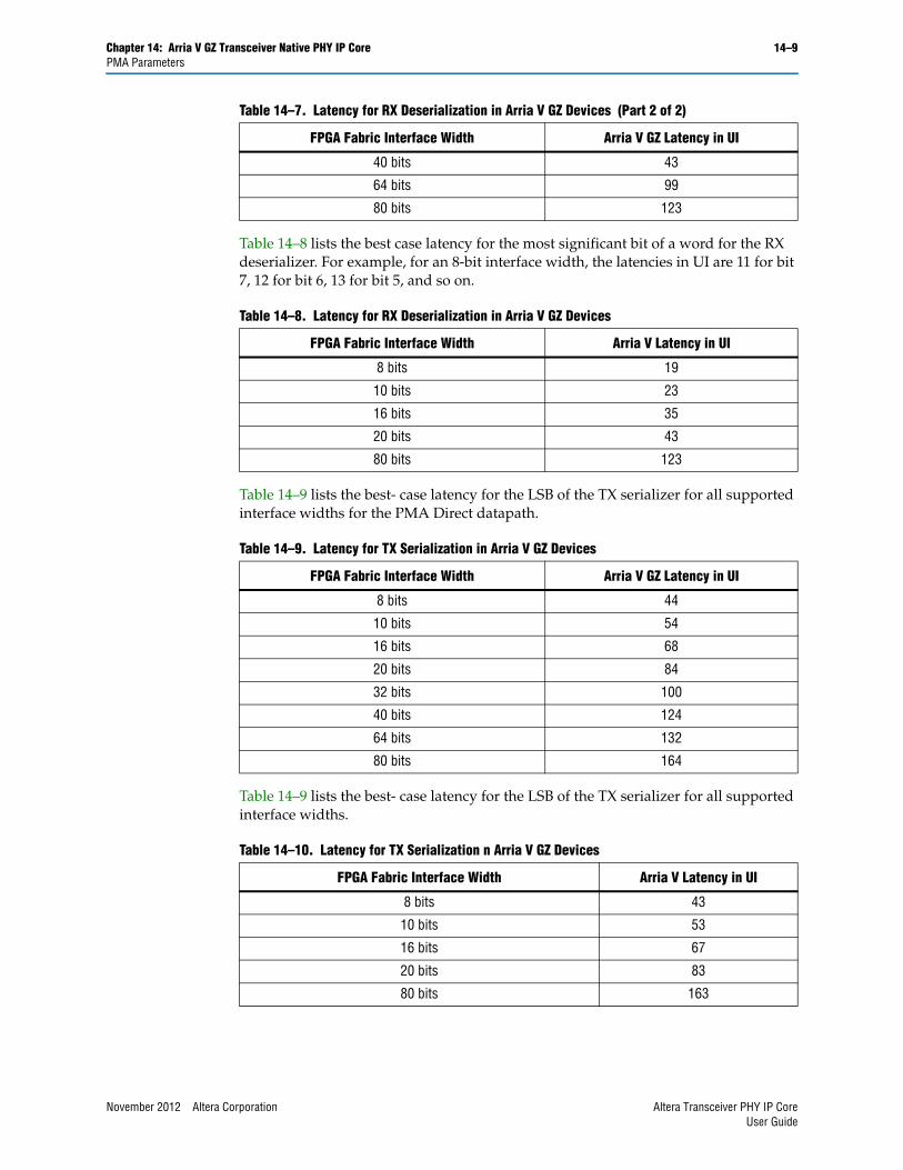
Chapter 14: Arria V GZ Transceiver Native PHY IP Core 14–9PMA Parameters
Table 14–8 lists the best case latency for the most significant bit of a word for the RX deserializer. For example, for an 8-bit interface width, the latencies in UI are 11 for bit 7, 12 for bit 6, 13 for bit 5, and so on.
Table 14–9 lists the best- case latency for the LSB of the TX serializer for all supported interface widths for the PMA Direct datapath.
Table 14–9 lists the best- case latency for the LSB of the TX serializer for all supported interface widths.
40 bits 43
64 bits 99
80 bits 123
Table 14–8. Latency for RX Deserialization in Arria V GZ Devices
FPGA Fabric Interface Width Arria V Latency in UI
8 bits 19
10 bits 23
16 bits 35
20 bits 43
80 bits 123
Table 14–9. Latency for TX Serialization in Arria V GZ Devices
FPGA Fabric Interface Width Arria V GZ Latency in UI
8 bits 44
10 bits 54
16 bits 68
20 bits 84
32 bits 100
40 bits 124
64 bits 132
80 bits 164
Table 14–10. Latency for TX Serialization n Arria V GZ Devices
FPGA Fabric Interface Width Arria V Latency in UI
8 bits 43
10 bits 53
16 bits 67
20 bits 83
80 bits 163
Table 14–7. Latency for RX Deserialization in Arria V GZ Devices (Part 2 of 2)
FPGA Fabric Interface Width Arria V GZ Latency in UI
November 2012 Altera Corporation Altera Transceiver PHY IP CoreUser Guide
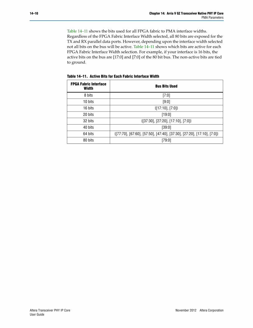
14–10 Chapter 14: Arria V GZ Transceiver Native PHY IP CorePMA Parameters
Table 14–11 shows the bits used for all FPGA fabric to PMA interface widths. Regardless of the FPGA Fabric Interface Width selected, all 80 bits are exposed for the TX and RX parallel data ports. However, depending upon the interface width selected not all bits on the bus will be active. Table 14–11 shows which bits are active for each FPGA Fabric Interface Width selection. For example, if your interface is 16 bits, the active bits on the bus are [17:0] and [7:0] of the 80 bit bus. The non-active bits are tied to ground.
Table 14–11. Active Bits for Each Fabric Interface Width
FPGA Fabric Interface Width Bus Bits Used
8 bits [7:0]
10 bits [9:0]
16 bits {[17:10], [7:0]}
20 bits [19:0]
32 bits {[37:30], [27:20], [17:10], [7:0]}
40 bits [39:0]
64 bits {[77:70], [67:60], [57:50], [47:40], [37:30], [27:20], [17:10], [7:0]}
80 bits [79:0]
Altera Transceiver PHY IP Core November 2012 Altera CorporationUser Guide
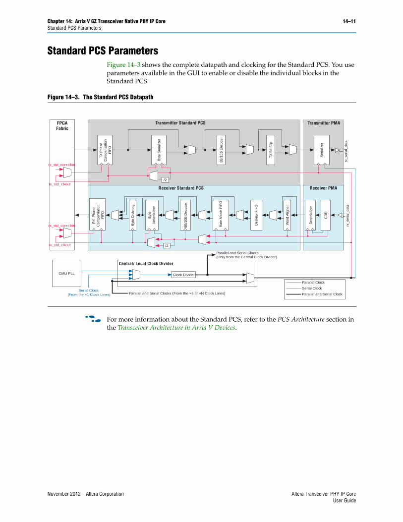
Chapter 14: Arria V GZ Transceiver Native PHY IP Core 14–11Standard PCS Parameters
Standard PCS ParametersFigure 14–3 shows the complete datapath and clocking for the Standard PCS. You use parameters available in the GUI to enable or disable the individual blocks in the Standard PCS.
f For more information about the Standard PCS, refer to the PCS Architecture section in the Transceiver Architecture in Arria V Devices.
Figure 14–3. The Standard PCS Datapath R
X P
hase
C
ompe
nsat
ion
FIFO
Byt
e O
rder
ing
Byt
eD
eser
ializ
er
8B/1
0B D
ecod
er
Rat
e M
atch
FIF
O
Receiver Standard PCS Receiver PMA
Des
kew
FIF
O
Wor
d A
ligne
r
Des
eria
lizer
CD
R
Transmitter Standard PCS Transmitter PMA
Ser
ializ
er
tx_s
eria
l_da
tarx
_ser
ial_
data
FPGAFabric
TX P
hase
C
ompe
nsat
ion
FIFO
Byt
e S
eria
lizer
8B/1
0B E
ncod
er
TX B
it S
lip
/2
/2
Parallel Clock
Serial Clock
Parallel and Serial Clock
Clock Divider
Parallel and Serial Clocks (From the ×6 or ×N Clock Lines)Serial Clock
(From the ×1 Clock Lines)
Central/ Local Clock Divider
Parallel and Serial Clocks(Only from the Central Clock Divider)
CMU PLL
tx_std_coreclkin
rx_std_coreclkin
rx_std_clkout
tx_std_clkout
November 2012 Altera Corporation Altera Transceiver PHY IP CoreUser Guide
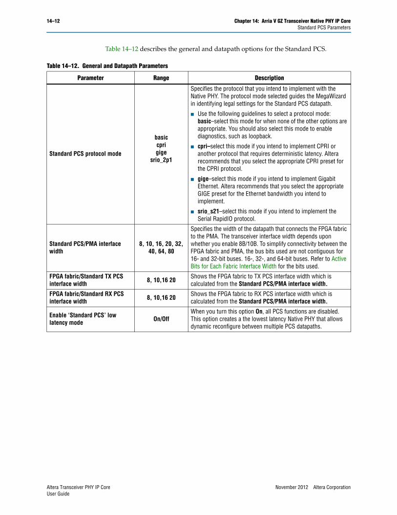
14–12 Chapter 14: Arria V GZ Transceiver Native PHY IP CoreStandard PCS Parameters
Table 14–12 describes the general and datapath options for the Standard PCS.
Table 14–12. General and Datapath Parameters
Parameter Range Description
Standard PCS protocol mode
basiccprigige
srio_2p1
Specifies the protocol that you intend to implement with the Native PHY. The protocol mode selected guides the MegaWizard in identifying legal settings for the Standard PCS datapath.
■ Use the following guidelines to select a protocol mode: basic–select this mode for when none of the other options are appropriate. You should also select this mode to enable diagnostics, such as loopback.
■ cpri–select this mode if you intend to implement CPRI or another protocol that requires deterministic latency. Altera recommends that you select the appropriate CPRI preset for the CPRI protocol.
■ gige–select this mode if you intend to implement Gigabit Ethernet. Altera recommends that you select the appropriate GIGE preset for the Ethernet bandwidth you intend to implement.
■ srio_s21–select this mode if you intend to implement the Serial RapidIO protocol.
Standard PCS/PMA interface width
8, 10, 16, 20, 32, 40, 64, 80
Specifies the width of the datapath that connects the FPGA fabric to the PMA. The transceiver interface width depends upon whether you enable 8B/10B. To simplify connectivity between the FPGA fabric and PMA, the bus bits used are not contiguous for 16- and 32-bit buses. 16-, 32-, and 64-bit buses. Refer to Active Bits for Each Fabric Interface Width for the bits used.
FPGA fabric/Standard TX PCS interface width 8, 10,16 20 Shows the FPGA fabric to TX PCS interface width which is
calculated from the Standard PCS/PMA interface width.
FPGA fabric/Standard RX PCS interface width 8, 10,16 20 Shows the FPGA fabric to RX PCS interface width which is
calculated from the Standard PCS/PMA interface width.
Enable ‘Standard PCS’ low latency mode On/Off
When you turn this option On, all PCS functions are disabled. This option creates a the lowest latency Native PHY that allows dynamic reconfigure between multiple PCS datapaths.
Altera Transceiver PHY IP Core November 2012 Altera CorporationUser Guide
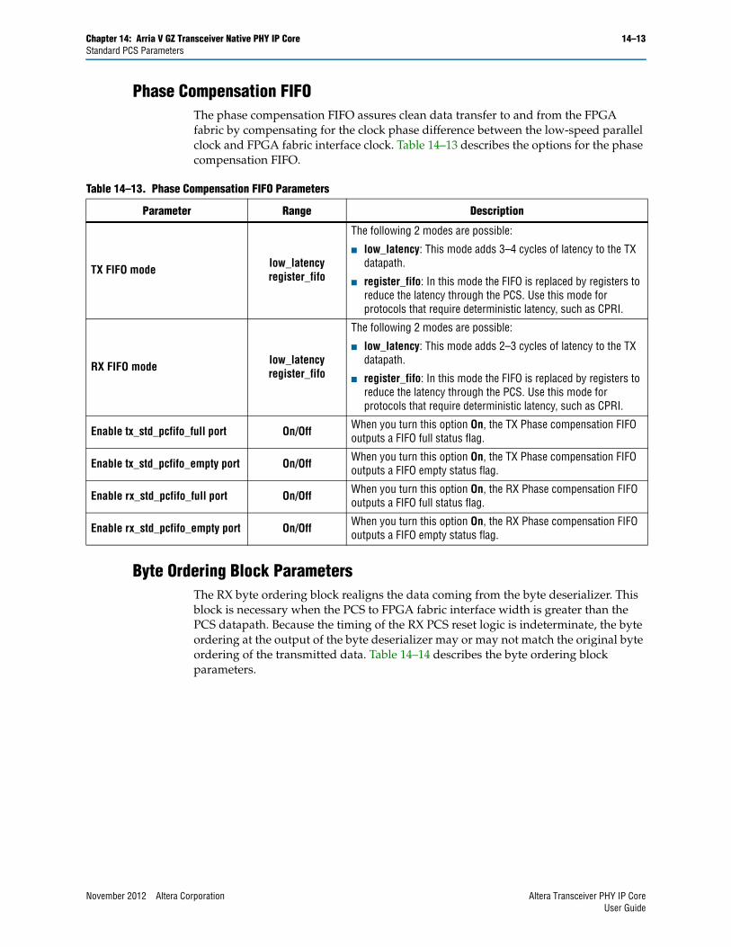
Chapter 14: Arria V GZ Transceiver Native PHY IP Core 14–13Standard PCS Parameters
Phase Compensation FIFOThe phase compensation FIFO assures clean data transfer to and from the FPGA fabric by compensating for the clock phase difference between the low-speed parallel clock and FPGA fabric interface clock. Table 14–13 describes the options for the phase compensation FIFO.
Byte Ordering Block ParametersThe RX byte ordering block realigns the data coming from the byte deserializer. This block is necessary when the PCS to FPGA fabric interface width is greater than the PCS datapath. Because the timing of the RX PCS reset logic is indeterminate, the byte ordering at the output of the byte deserializer may or may not match the original byte ordering of the transmitted data. Table 14–14 describes the byte ordering block parameters.
Table 14–13. Phase Compensation FIFO Parameters
Parameter Range Description
TX FIFO mode low_latencyregister_fifo
The following 2 modes are possible:
■ low_latency: This mode adds 3–4 cycles of latency to the TX datapath.
■ register_fifo: In this mode the FIFO is replaced by registers to reduce the latency through the PCS. Use this mode for protocols that require deterministic latency, such as CPRI.
RX FIFO mode low_latencyregister_fifo
The following 2 modes are possible:
■ low_latency: This mode adds 2–3 cycles of latency to the TX datapath.
■ register_fifo: In this mode the FIFO is replaced by registers to reduce the latency through the PCS. Use this mode for protocols that require deterministic latency, such as CPRI.
Enable tx_std_pcfifo_full port On/Off When you turn this option On, the TX Phase compensation FIFO outputs a FIFO full status flag.
Enable tx_std_pcfifo_empty port On/Off When you turn this option On, the TX Phase compensation FIFO outputs a FIFO empty status flag.
Enable rx_std_pcfifo_full port On/Off When you turn this option On, the RX Phase compensation FIFO outputs a FIFO full status flag.
Enable rx_std_pcfifo_empty port On/Off When you turn this option On, the RX Phase compensation FIFO outputs a FIFO empty status flag.
November 2012 Altera Corporation Altera Transceiver PHY IP CoreUser Guide
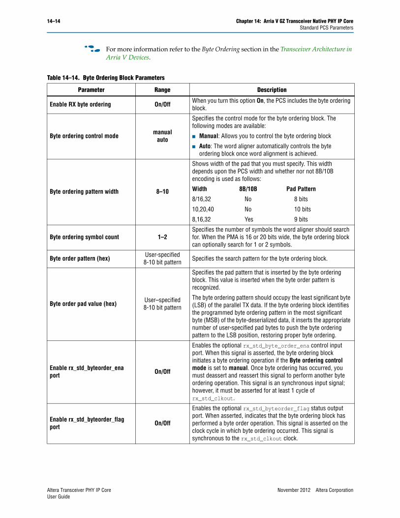
14–14 Chapter 14: Arria V GZ Transceiver Native PHY IP CoreStandard PCS Parameters
f For more information refer to the Byte Ordering section in the Transceiver Architecture in Arria V Devices.
Table 14–14. Byte Ordering Block Parameters
Parameter Range Description
Enable RX byte ordering On/Off When you turn this option On, the PCS includes the byte ordering block.
Byte ordering control mode manualauto
Specifies the control mode for the byte ordering block. The following modes are available:
■ Manual: Allows you to control the byte ordering block
■ Auto: The word aligner automatically controls the byte ordering block once word alignment is achieved.
Byte ordering pattern width 8–10
Shows width of the pad that you must specify. This width depends upon the PCS width and whether nor not 8B/10B encoding is used as follows:
Width 8B/10B Pad Pattern
8/16,32 No 8 bits
10,20,40 No 10 bits
8,16,32 Yes 9 bits
Byte ordering symbol count 1–2Specifies the number of symbols the word aligner should search for. When the PMA is 16 or 20 bits wide, the byte ordering block can optionally search for 1 or 2 symbols.
Byte order pattern (hex) User-specified 8-10 bit pattern Specifies the search pattern for the byte ordering block.
Byte order pad value (hex) User–specified 8-10 bit pattern
Specifies the pad pattern that is inserted by the byte ordering block. This value is inserted when the byte order pattern is recognized.
The byte ordering pattern should occupy the least significant byte (LSB) of the parallel TX data. If the byte ordering block identifies the programmed byte ordering pattern in the most significant byte (MSB) of the byte-deserialized data, it inserts the appropriate number of user-specified pad bytes to push the byte ordering pattern to the LSB position, restoring proper byte ordering.
Enable rx_std_byteorder_ena port On/Off
Enables the optional rx_std_byte_order_ena control input port. When this signal is asserted, the byte ordering block initiates a byte ordering operation if the Byte ordering control mode is set to manual. Once byte ordering has occurred, you must deassert and reassert this signal to perform another byte ordering operation. This signal is an synchronous input signal; however, it must be asserted for at least 1 cycle of rx_std_clkout.
Enable rx_std_byteorder_flag port On/Off
Enables the optional rx_std_byteorder_flag status output port. When asserted, indicates that the byte ordering block has performed a byte order operation. This signal is asserted on the clock cycle in which byte ordering occurred. This signal is synchronous to the rx_std_clkout clock.
Altera Transceiver PHY IP Core November 2012 Altera CorporationUser Guide
Chapter 14: Arria V GZ Transceiver Native PHY IP Core 14–15Standard PCS Parameters
Byte Serializer and DeserializerThe byte serializer and deserializer allow the PCS to operate at twice the data width of the PMA serializer. This feature allows the PCS to run at a lower frequency and accommodate a wider range of FPGA interface widths. Table 14–15 describes the byte serialization and deserialization options you can specify.
f For more information, refer to the Byte Ordering section in the Transceiver Architecture in Arria V Devices.
8B/10BThe 8B/10B encoder generates 10-bit code groups from the 8-bit data and 1-bit control identifier. In 8-bit width mode, the 8B/10B encoder translates the 8-bit data to a 10-bit code group (control word or data word) with proper disparity. The 8B/10B decoder decodes the data into an 8-bit data and 1-bit control identifier. Table 14–16 describes the 8B/10B encoder and decoder options.
f
Rate Match FIFOThe rate match FIFO compensates for the very small frequency differences between the local system clock and the RX recovered clock. Table 14–17 describes the rate match FIFO parameters.
Table 14–15. Byte Serializer and Deserializer Parameters
Parameter Range Description
Enable TX byte serializer On/OffWhen you turn this option On, the PCS includes a TX byte serializer which allows the PCS to run at a lower clock frequency to accommodate a wider range of FPGA interface widths.
Enable RX byte deserializer On/Off
When you turn this option On, the PCS includes an RX byte deserializer and deserializer which allows the PCS to run at a lower clock frequency to accommodate a wider range of FPGA interface widths.
Table 14–16. 8B/10B Encoder and Decoder Parameters
Parameter Range Description
Enable TX 8B/10B encoder On/Off When you turn this option On, the PCS includes the 8B/10B encoder.
Enable TX 8B/10B disparity control On/Off
When you turn this option On, the PCS includes disparity control for the 8B/10B encoder. Your force the disparity of the 8B/10B encoder using the tx_forcedisp control signal.
Enable RX 8B/10B decoder On/Off When you turn this option On, the PCS includes the 8B/10B decoder.
November 2012 Altera Corporation Altera Transceiver PHY IP CoreUser Guide
14–16 Chapter 14: Arria V GZ Transceiver Native PHY IP CoreStandard PCS Parameters
f
Word Aligner and Bit-Slip ParametersThe word aligner aligns the data coming from RX PMA deserializer to a given word boundary. When the word aligner operates in bit-slip mode, the word aligner slips a single bit for every rising edge of the bit slip control signal.Table 14–18 describes the word aligner and bit-slip parameters.
f
Table 14–17. Rate Match FIFO Parameters
Parameter Range Description
Enable RX rate match FIFO On/OffWhen you turn this option On, the PCS includes a FIFO to compensate for the very small frequency differences between the local system clock and the RX recovered clock.
RX rate match insert/delete +ve pattern (hex)
User-specified 20 bit pattern
Specifies the +ve (positive) disparity value for the RX rate match FIFO as a hexadecimal string.
RX rate match insert/delete -ve pattern (hex)
User-specified 20 bit pattern
Specifies the -ve (negative) disparity value for the RX rate match FIFO as a hexadecimal string.
Enable rx_std_rm_fifo_empty port On/Off
When you turn this option On, the rate match FIFO outputs a FIFO empty status flag. The rate match FIFO compensates for small clock frequency differences between the upstream transmitter and the local receiver clocks by inserting or removing skip (SKP) symbols or ordered sets from the inter-packet gap (IPG) or idle stream.
Enable rx_std_rm_fifo_full port On/Off When you turn this option On, the rate match FIFO outputs a FIFO full status flag.
Table 14–18. Word Aligner and Bit-Slip Parameters (Part 1 of 2)
Parameter Range Description
Enable TX bit-slip On/OffWhen you turn this option On, the PCS includes the bit-slip function. The outgoing TX data can be slipped by the number of bits specified by the tx_bitslipboundarysel control signal.
Enable tx_std_bitslipboundarysel control input port.
On/Off When you turn this option On, the PCS includes the optional tx_std_bitslipboundarysel control input port.
RX word aligner modebit_silpsync_smmanual
Specifies one of the following 3 modes for the word aligner:
■ Bit_slip: You can use bit slip mode to shift the word boundary. For every rising edge of the rx_bitslip signal, the word boundary is shifted by 1 bit. Each bit-slip removes the earliest received bit from the received data
■ Sync_sm: In synchronous state machine mode, a programmable state machine controls word alignment. You can only use this mode with 8B/10B encoding. The data width at the word aligner can be 10 or 20 bits
■ Manual: This mode Enables word alignment by asserting the rx_std_wa_patternalign. This is an edge sensitive signal.
Altera Transceiver PHY IP Core November 2012 Altera CorporationUser Guide
Chapter 14: Arria V GZ Transceiver Native PHY IP Core 14–17Standard PCS Parameters
Bit Reversal and Polarity InversionThese functions allow you to reverse bit order, byte order, and polarity to correct errors and to accommodate different layouts of data. Table 14–19 describes these parameters.
RX word aligner pattern length 7,8,10,16,20,32 Specifies the length of the pattern the word aligner uses for alignment.
RX word aligner pattern (hex) User-specified Specifies the word aligner pattern in hex.
Number of word alignment patterns to achieve sync 1–256
Specifies the number of valid word alignment patterns that must be received before the word aligner achieves synchronization lock. The default is 3.
Number of invalid words to lose sync 1–256
Specifies the number of invalid data codes or disparity errors that must be received before the word aligner loses synchronization. The default is 3.
Number of valid data words to decrement error count 1–256
Specifies the number of valid data codes that must be received to decrement the error counter. If the word aligner receives enough valid data codes to decrement the error count to 0, the word aligner returns to synchronization lock.
Run length detector word count 0–63Specifies the maximum number of contiguous 0s or 1s in the data stream before the word aligner reports a run length violation.
Enable rx_std_wa_patternalign port On/Off
Enables the optional rx_std_wa_patternalign control input port. A rising edge on this signal causes the word aligner to align the next incoming word alignment pattern when the word aligner is configured in manual mode.
Enable rx_std_wa_a1a2size port On/Off Enables the optional rx_std_wa_a1a2size control input port.
Enable rx_std_wa_bitslipboundarysel port
On/Off Enables the optional rx_std_wa_bitslipboundarysel status output port.
Enable rx_std_wa_bitslip port On/Off Enables the optional rx_std_wa_bitslip control input port.
Enable rx_std_wa_runlength_err port On/Off Enables the optional rx_std_wa_runlength_err control input
port.
Table 14–18. Word Aligner and Bit-Slip Parameters (Part 2 of 2)
Parameter Range Description
Table 14–19. Bit Reversal and Polarity Inversion Parameters (Part 1 of 2)
Parameter Range Description
Enable TX bit reversal On/Off
When you turn this option On, the word aligner reverses TX parallel data before transmitting it to the PMA for serialization. You can only change this static setting using the Transceiver Reconfiguration Controller.
Enable RX bit reversal On/OffWhen you turn this option On, the rx_st_bitrev_ena port controls bit reversal of the RX parallel data after it passes from the PMA to the PCS.
Enable RX byte reversal On/Off
When you turn this option On, the word aligner reverses the byte order before transmitting data. This function allows you to reverse the order of bytes that were erroneously swapped. The PCS can swap the ordering of both 8 and10 bit words.
November 2012 Altera Corporation Altera Transceiver PHY IP CoreUser Guide
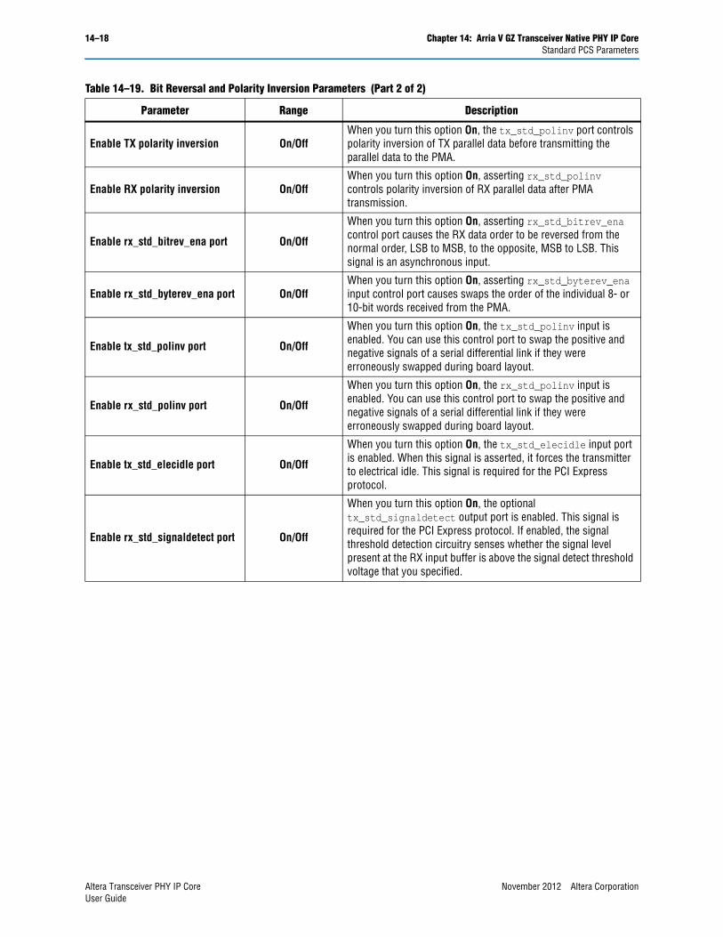
14–18 Chapter 14: Arria V GZ Transceiver Native PHY IP CoreStandard PCS Parameters
Enable TX polarity inversion On/OffWhen you turn this option On, the tx_std_polinv port controls polarity inversion of TX parallel data before transmitting the parallel data to the PMA.
Enable RX polarity inversion On/OffWhen you turn this option On, asserting rx_std_polinv controls polarity inversion of RX parallel data after PMA transmission.
Enable rx_std_bitrev_ena port On/Off
When you turn this option On, asserting rx_std_bitrev_ena control port causes the RX data order to be reversed from the normal order, LSB to MSB, to the opposite, MSB to LSB. This signal is an asynchronous input.
Enable rx_std_byterev_ena port On/OffWhen you turn this option On, asserting rx_std_byterev_ena input control port causes swaps the order of the individual 8- or 10-bit words received from the PMA.
Enable tx_std_polinv port On/Off
When you turn this option On, the tx_std_polinv input is enabled. You can use this control port to swap the positive and negative signals of a serial differential link if they were erroneously swapped during board layout.
Enable rx_std_polinv port On/Off
When you turn this option On, the rx_std_polinv input is enabled. You can use this control port to swap the positive and negative signals of a serial differential link if they were erroneously swapped during board layout.
Enable tx_std_elecidle port On/Off
When you turn this option On, the tx_std_elecidle input port is enabled. When this signal is asserted, it forces the transmitter to electrical idle. This signal is required for the PCI Express protocol.
Enable rx_std_signaldetect port On/Off
When you turn this option On, the optional tx_std_signaldetect output port is enabled. This signal is required for the PCI Express protocol. If enabled, the signal threshold detection circuitry senses whether the signal level present at the RX input buffer is above the signal detect threshold voltage that you specified.
Table 14–19. Bit Reversal and Polarity Inversion Parameters (Part 2 of 2)
Parameter Range Description
Altera Transceiver PHY IP Core November 2012 Altera CorporationUser Guide
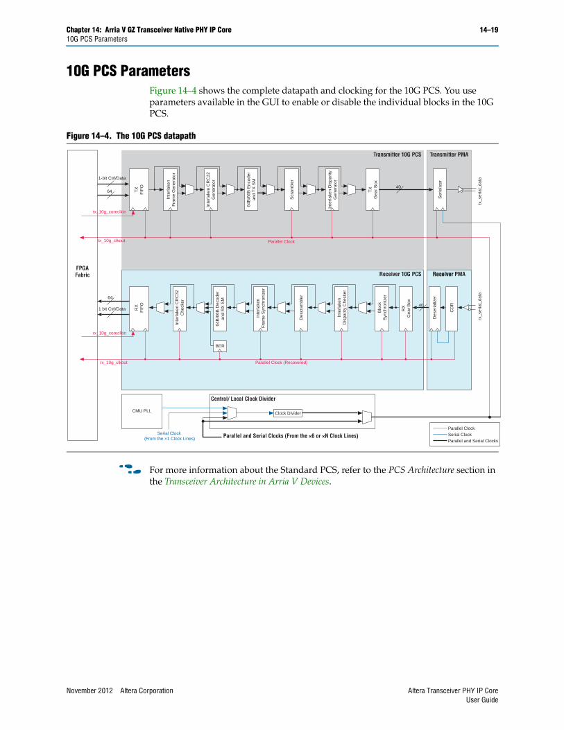
Chapter 14: Arria V GZ Transceiver Native PHY IP Core 14–1910G PCS Parameters
10G PCS ParametersFigure 14–4 shows the complete datapath and clocking for the 10G PCS. You use parameters available in the GUI to enable or disable the individual blocks in the 10G PCS.
f For more information about the Standard PCS, refer to the PCS Architecture section in the Transceiver Architecture in Arria V Devices.
Figure 14–4. The 10G PCS datapath
FPGAFabric
Transmitter 10G PCS
Receiver 10G PCS
Transmitter PMA
Receiver Receiver PMA
TX
FIF
OR
XF
IFO
Inte
rlake
nFr
ame
Gen
erat
or
Inte
rlake
n C
RC
32G
ener
ator
Inte
rlake
n C
RC
32C
heck
er
64B
/66B
Enc
oder
and
TX
SM
64B
/66B
Dec
oder
and
RX
SM
Scr
ambl
er
Des
cram
bler
Inte
rlake
nD
ispa
rity
Che
cker
Blo
ckS
ynch
roni
zer
Inte
rlake
nFr
ame
Syn
chro
nize
r
Inte
rlake
n D
ispa
rity
Gen
erat
or
TX
Gea
r B
ox
RX
Gea
r B
ox
64
64
Parallel Clock (Recovered)
Parallel Clock
40
Ser
ializ
erD
eser
ializ
er
CD
R
tx_s
eria
l_da
tarx
_ser
ial_
data
1-bit Ctrl/Data
1 bit Ctrl/Data40
Clock Divider
BER
Parallel and Serial Clocks (From the ×6 or ×N Clock Lines)Serial Clock (From the ×1 Clock Lines)
Central/ Local Clock Divider
Parallel ClockSerial ClockParallel and Serial Clocks
CMU PLL
tx_10g_coreclkin
rx_10g_coreclkin
tx_10g_clkout
rx_10g_clkout
November 2012 Altera Corporation Altera Transceiver PHY IP CoreUser Guide
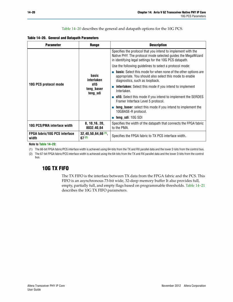
14–20 Chapter 14: Arria V GZ Transceiver Native PHY IP Core10G PCS Parameters
Table 14–20 describes the general and datapath options for the 10G PCS.
10G TX FIFOThe TX FIFO is the interface between TX data from the FPGA fabric and the PCS. This FIFO is an asynchronous 73-bit wide, 32-deep memory buffer It also provides full, empty, partially full, and empty flags based on programmable thresholds. Table 14–21 describes the 10G TX FIFO parameters.
Table 14–20. General and Datapath Parameters
Parameter Range Description
10G PCS protocol mode
basicinterlaken
sfi5teng_baser
teng_sdi
Specifies the protocol that you intend to implement with the Native PHY. The protocol mode selected guides the MegaWizard in identifying legal settings for the 10G PCS datapath.
Use the following guidelines to select a protocol mode:
■ basic: Select this mode for when none of the other options are appropriate. You should also select this mode to enable diagnostics, such as loopback.
■ interlaken: Select this mode if you intend to implement Interlaken.
■ sfi5: Select this mode if you intend to implement the SERDES Framer Interface Level 5 protocol.
■ teng_baser: select this mode if you intend to implement the 10GBASE-R protocol.
■ teng_sdi: 10G SDI
10G PCS/PMA interface width 8, 10,16, 20, 8032.40,64
Specifies the width of the datapath that connects the FPGA fabric to the PMA.
FPGA fabric/10G PCS interface width
32,40,50,64,66 (1),67 (2) Specifies the FPGA fabric to TX PCS interface width.
Note to Table 14–20:
(1) The 66-bit FPGA fabric/PCS interface width is achieved using 64-bits from the TX and RX parallel data and the lower 2-bits from the control bus.(2) The 67-bit FPGA fabric/PCS interface width is achieved using the 64-bits from the TX and RX parallel data and the lower 3-bits from the control
bus.
Altera Transceiver PHY IP Core November 2012 Altera CorporationUser Guide
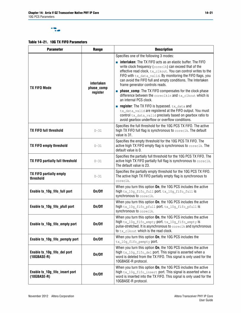
Chapter 14: Arria V GZ Transceiver Native PHY IP Core 14–2110G PCS Parameters
f
Table 14–21. 10G TX FIFO Parameters
Parameter Range Description
TX FIFO Modeinterlaken
phase_compregister
Specifies one of the following 3 modes:
■ interlaken: The TX FIFO acts as an elastic buffer. The FIFO write clock frequency (coreclk) can exceed that of the effective read clock, tx_clkout. You can control writes to the FIFO with tx_data_valid. By monitoring the FIFO flags, you can avoid the FIFO full and empty conditions. The Interlaken frame generator controls reads.
■ phase_comp: The TX FIFO compensates for the clock phase difference between the coreclkin and tx_clkout which is an internal PCS clock.
■ register: The TX FIFO is bypassed. tx_data and tx_data_valid are registered at the FIFO output. You must control tx_data_valid precisely based on gearbox ratio to avoid gearbox underflow or overflow conditions.
TX FIFO full threshold 0–31Specifies the full threshold for the 10G PCS TX FIFO. The active high TX FIFO full flag is synchronous to coreclk. The default value is 31.
TX FIFO empty threshold 0–31Specifies the empty threshold for the 10G PCS TX FIFO. The active high TX FIFO empty flag is synchronous to coreclk. The default value is 0.
TX FIFO partially full threshold 0–31Specifies the partially full threshold for the 10G PCS TX FIFO. The active high TX FIFO partially full flag is synchronous to coreclk. The default value is 23.
TX FIFO partially empty threshold 0–31
Specifies the partially empty threshold for the 10G PCS TX FIFO. The active high TX FIFO partially empty flag is synchronous to coreclk.
Enable tx_10g_fifo_full port On/OffWhen you turn this option On, the 10G PCS includes the active high tx_10g_fifo_full port. tx_10g_fifo_full is synchronous to coreclk.
Enable tx_10g_fifo_pfull port On/OffWhen you turn this option On, the 10G PCS includes the active high tx_10g_fifo_pfull port. tx_10g_fifo_pfull is synchronous to coreclk.
Enable tx_10g_fifo_empty port On/Off
When you turn this option On, the 10G PCS includes the active high tx_10g_fifo_empty port. tx_10g_fifo_empty is pulse-stretched. It is asynchronous to coreclk and synchronous to tx_clkout which is the read clock.
Enable tx_10g_fifo_pempty port On/Off When you turn this option On, the 10G PCS includes the tx_10g_fifo_pempty port.
Enable tx_10g_fifo_del port (10GBASE-R) On/Off
When you turn this option On, the 10G PCS includes the active high tx_10g_fifo_del port. This signal is asserted when a word is deleted from the TX FIFO. This signal is only used for the 10GBASE-R protocol.
Enable tx_10g_fifo_insert port (10GBASE-R) On/Off
When you turn this option On, the 10G PCS includes the active high tx_10g_fifo_insert port. This signal is asserted when a word is inserted into the TX FIFO. This signal is only used for the 10GBASE-R protocol.
November 2012 Altera Corporation Altera Transceiver PHY IP CoreUser Guide
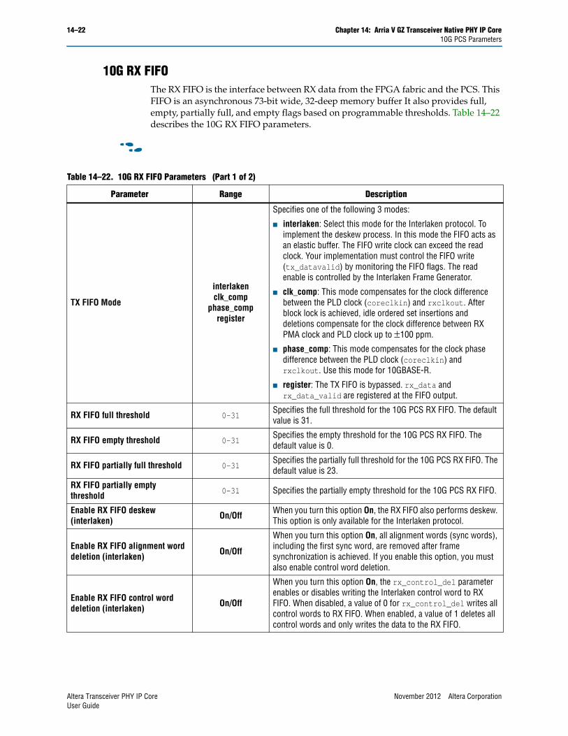
14–22 Chapter 14: Arria V GZ Transceiver Native PHY IP Core10G PCS Parameters
10G RX FIFOThe RX FIFO is the interface between RX data from the FPGA fabric and the PCS. This FIFO is an asynchronous 73-bit wide, 32-deep memory buffer It also provides full, empty, partially full, and empty flags based on programmable thresholds. Table 14–22 describes the 10G RX FIFO parameters.
f
Table 14–22. 10G RX FIFO Parameters (Part 1 of 2)
Parameter Range Description
TX FIFO Mode
interlakenclk_comp
phase_compregister
Specifies one of the following 3 modes:
■ interlaken: Select this mode for the Interlaken protocol. To implement the deskew process. In this mode the FIFO acts as an elastic buffer. The FIFO write clock can exceed the read clock. Your implementation must control the FIFO write (tx_datavalid) by monitoring the FIFO flags. The read enable is controlled by the Interlaken Frame Generator.
■ clk_comp: This mode compensates for the clock difference between the PLD clock (coreclkin) and rxclkout. After block lock is achieved, idle ordered set insertions and deletions compensate for the clock difference between RX PMA clock and PLD clock up to 100 ppm.
■ phase_comp: This mode compensates for the clock phase difference between the PLD clock (coreclkin) and rxclkout. Use this mode for 10GBASE-R.
■ register: The TX FIFO is bypassed. rx_data and rx_data_valid are registered at the FIFO output.
RX FIFO full threshold 0–31Specifies the full threshold for the 10G PCS RX FIFO. The default value is 31.
RX FIFO empty threshold 0–31Specifies the empty threshold for the 10G PCS RX FIFO. The default value is 0.
RX FIFO partially full threshold 0–31Specifies the partially full threshold for the 10G PCS RX FIFO. The default value is 23.
RX FIFO partially empty threshold 0–31 Specifies the partially empty threshold for the 10G PCS RX FIFO.
Enable RX FIFO deskew (interlaken) On/Off When you turn this option On, the RX FIFO also performs deskew.
This option is only available for the Interlaken protocol.
Enable RX FIFO alignment word deletion (interlaken) On/Off
When you turn this option On, all alignment words (sync words), including the first sync word, are removed after frame synchronization is achieved. If you enable this option, you must also enable control word deletion.
Enable RX FIFO control word deletion (interlaken) On/Off
When you turn this option On, the rx_control_del parameter enables or disables writing the Interlaken control word to RX FIFO. When disabled, a value of 0 for rx_control_del writes all control words to RX FIFO. When enabled, a value of 1 deletes all control words and only writes the data to the RX FIFO.
Altera Transceiver PHY IP Core November 2012 Altera CorporationUser Guide
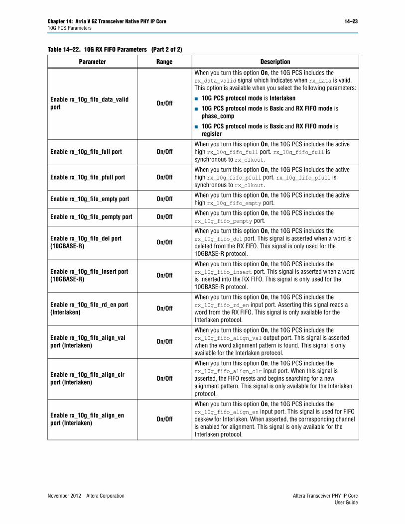
Chapter 14: Arria V GZ Transceiver Native PHY IP Core 14–2310G PCS Parameters
Enable rx_10g_fifo_data_valid port On/Off
When you turn this option On, the 10G PCS includes the rx_data_valid signal which Indicates when rx_data is valid. This option is available when you select the following parameters:
■ 10G PCS protocol mode is Interlaken
■ 10G PCS protocol mode is Basic and RX FIFO mode is phase_comp
■ 10G PCS protocol mode is Basic and RX FIFO mode is register
Enable rx_10g_fifo_full port On/OffWhen you turn this option On, the 10G PCS includes the active high rx_10g_fifo_full port. rx_10g_fifo_full is synchronous to rx_clkout.
Enable rx_10g_fifo_pfull port On/OffWhen you turn this option On, the 10G PCS includes the active high rx_10g_fifo_pfull port. rx_10g_fifo_pfull is synchronous to rx_clkout.
Enable rx_10g_fifo_empty port On/Off When you turn this option On, the 10G PCS includes the active high rx_10g_fifo_empty port.
Enable rx_10g_fifo_pempty port On/Off When you turn this option On, the 10G PCS includes the rx_10g_fifo_pempty port.
Enable rx_10g_fifo_del port (10GBASE-R) On/Off
When you turn this option On, the 10G PCS includes the rx_10g_fifo_del port. This signal is asserted when a word is deleted from the RX FIFO. This signal is only used for the 10GBASE-R protocol.
Enable rx_10g_fifo_insert port (10GBASE-R) On/Off
When you turn this option On, the 10G PCS includes the rx_10g_fifo_insert port. This signal is asserted when a word is inserted into the RX FIFO. This signal is only used for the 10GBASE-R protocol.
Enable rx_10g_fifo_rd_en port (Interlaken) On/Off
When you turn this option On, the 10G PCS includes the rx_10g_fifo_rd_en input port. Asserting this signal reads a word from the RX FIFO. This signal is only available for the Interlaken protocol.
Enable rx_10g_fifo_align_val port (Interlaken) On/Off
When you turn this option On, the 10G PCS includes the rx_10g_fifo_align_val output port. This signal is asserted when the word alignment pattern is found. This signal is only available for the Interlaken protocol.
Enable rx_10g_fifo_align_clr port (Interlaken) On/Off
When you turn this option On, the 10G PCS includes the rx_10g_fifo_align_clr input port. When this signal is asserted, the FIFO resets and begins searching for a new alignment pattern. This signal is only available for the Interlaken protocol.
Enable rx_10g_fifo_align_en port (Interlaken) On/Off
When you turn this option On, the 10G PCS includes the rx_10g_fifo_align_en input port. This signal is used for FIFO deskew for Interlaken. When asserted, the corresponding channel is enabled for alignment. This signal is only available for the Interlaken protocol.
Table 14–22. 10G RX FIFO Parameters (Part 2 of 2)
Parameter Range Description
November 2012 Altera Corporation Altera Transceiver PHY IP CoreUser Guide
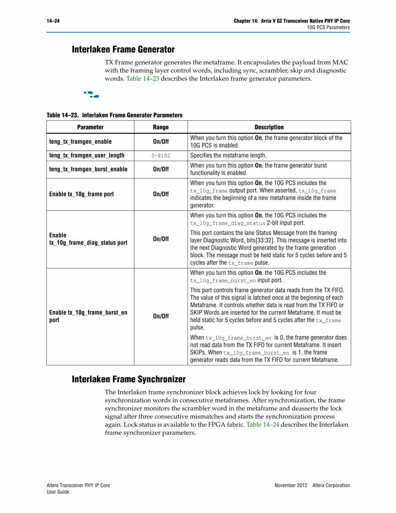
14–24 Chapter 14: Arria V GZ Transceiver Native PHY IP Core10G PCS Parameters
Interlaken Frame Generator TX Frame generator generates the metaframe. It encapsulates the payload from MAC with the framing layer control words, including sync, scrambler, skip and diagnostic words. Table 14–23 describes the Interlaken frame generator parameters.
f
Interlaken Frame SynchronizerThe Interlaken frame synchronizer block achieves lock by looking for four synchronization words in consecutive metaframes. After synchronization, the frame synchronizer monitors the scrambler word in the metaframe and deasserts the lock signal after three consecutive mismatches and starts the synchronization process again. Lock status is available to the FPGA fabric. Table 14–24 describes the Interlaken frame synchronizer parameters.
Table 14–23. Interlaken Frame Generator Parameters
Parameter Range Description
teng_tx_framgen_enable On/Off When you turn this option On, the frame generator block of the 10G PCS is enabled.
teng_tx_framgen_user_length 0-8192 Specifies the metaframe length.
teng_tx_framgen_burst_enable On/Off When you turn this option On, the frame generator burst functionality is enabled.
Enable tx_10g_frame port On/Off
When you turn this option On, the 10G PCS includes the tx_10g_frame output port. When asserted, tx_10g_frame indicates the beginning of a new metaframe inside the frame generator.
Enable tx_10g_frame_diag_status port On/Off
When you turn this option On, the 10G PCS includes the tx_10g_frame_diag_status 2-bit input port.
This port contains the lane Status Message from the framing layer Diagnostic Word, bits[33:32]. This message is inserted into the next Diagnostic Word generated by the frame generation block. The message must be held static for 5 cycles before and 5 cycles after the tx_frame pulse.
Enable tx_10g_frame_burst_en port On/Off
When you turn this option On, the 10G PCS includes the tx_10g_frame_burst_en input port.
This port controls frame generator data reads from the TX FIFO. The value of this signal is latched once at the beginning of each Metaframe. It controls whether data is read from the TX FIFO or SKIP Words are inserted for the current Metaframe. It must be held static for 5 cycles before and 5 cycles after the tx_frame pulse.
When tx_10g_frame_burst_en is 0, the frame generator does not read data from the TX FIFO for current Metaframe. It insert SKIPs. When tx_10g_frame_burst_en is 1, the frame generator reads data from the TX FIFO for current Metaframe.
Altera Transceiver PHY IP Core November 2012 Altera CorporationUser Guide
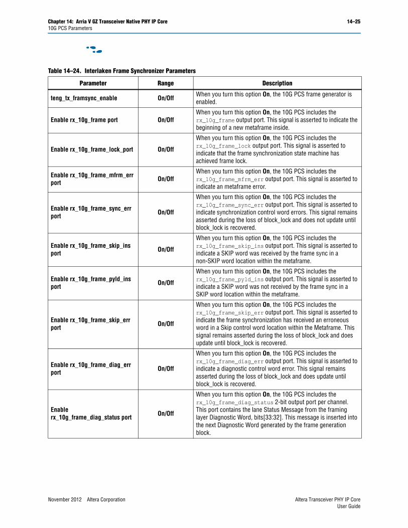
Chapter 14: Arria V GZ Transceiver Native PHY IP Core 14–2510G PCS Parameters
f
Table 14–24. Interlaken Frame Synchronizer Parameters
Parameter Range Description
teng_tx_framsync_enable On/Off When you turn this option On, the 10G PCS frame generator is enabled.
Enable rx_10g_frame port On/OffWhen you turn this option On, the 10G PCS includes the rx_10g_frame output port. This signal is asserted to indicate the beginning of a new metaframe inside.
Enable rx_10g_frame_lock_port On/Off
When you turn this option On, the 10G PCS includes the rx_10g_frame_lock output port. This signal is asserted to indicate that the frame synchronization state machine has achieved frame lock.
Enable rx_10g_frame_mfrm_err port On/Off
When you turn this option On, the 10G PCS includes the rx_10g_frame_mfrm_err output port. This signal is asserted to indicate an metaframe error.
Enable rx_10g_frame_sync_err port On/Off
When you turn this option On, the 10G PCS includes the rx_10g_frame_sync_err output port. This signal is asserted to indicate synchronization control word errors. This signal remains asserted during the loss of block_lock and does not update until block_lock is recovered.
Enable rx_10g_frame_skip_ins port On/Off
When you turn this option On, the 10G PCS includes the rx_10g_frame_skip_ins output port. This signal is asserted to indicate a SKIP word was received by the frame sync in a non-SKIP word location within the metaframe.
Enable rx_10g_frame_pyld_ins port On/Off
When you turn this option On, the 10G PCS includes the rx_10g_frame_pyld_ins output port. This signal is asserted to indicate a SKIP word was not received by the frame sync in a SKIP word location within the metaframe.
Enable rx_10g_frame_skip_err port On/Off
When you turn this option On, the 10G PCS includes the rx_10g_frame_skip_err output port. This signal is asserted to indicate the frame synchronization has received an erroneous word in a Skip control word location within the Metaframe. This signal remains asserted during the loss of block_lock and does update until block_lock is recovered.
Enable rx_10g_frame_diag_err port On/Off
When you turn this option On, the 10G PCS includes the rx_10g_frame_diag_err output port. This signal is asserted to indicate a diagnostic control word error. This signal remains asserted during the loss of block_lock and does update until block_lock is recovered.
Enable rx_10g_frame_diag_status port On/Off
When you turn this option On, the 10G PCS includes the rx_10g_frame_diag_status 2-bit output port per channel. This port contains the lane Status Message from the framing layer Diagnostic Word, bits[33:32]. This message is inserted into the next Diagnostic Word generated by the frame generation block.
November 2012 Altera Corporation Altera Transceiver PHY IP CoreUser Guide
14–26 Chapter 14: Arria V GZ Transceiver Native PHY IP Core10G PCS Parameters
Interlaken CRC32 Generator and CheckerCRC-32 provides a diagnostic tool on a per-lane basis. You can use CRC-32 to trace interface errors back to an individual lane. The CRC-32 calculation covers the whole metaframe including the Diagnostic Word itself. This CRC code value is stored in the CRC32 field of the Diagnostic Word. Table 14–25 describes the CRC-32 parameters.
f
10GBASE-R BER CheckerThe BER monitor block conforms to the 10GBASE-R protocol specification as described in IEEE 802.3-2008 Clause-49. After block lock is achieved, the BER monitor starts to count the number of invalid synchronization headers within a 125-s period. If more than 16 invalid synchronization headers are observed in a 125-s period, the BER monitor provides the status signal to the FPGA fabric, indicating a high bit error. Table 14–26 describes the 10GBASE-R BER checker parameters.
f
Table 14–25. Interlaken CRC32 Generator and Checker Parameters
Parameter Range Description
Enable Interlaken TX CRC32 Generator On/Off When you turn this option On, the TX 10G PCS datapath includes
the CRC32 function.
Enable Interlaken RX CRC32 Generator On/Off When you turn this option On, the RX 10G PCS datapath includes
the CRC32 function.
Enable rx_10g_crc32_err port On/OffWhen you turn this option On, the 10G PCS includes the rx_10g_crc32_err port. This signal is asserted to indicate that the CRC checker has found an error in the current metaframe.
Table 14–26. 10GBASE-R BER Checker Parameters
Parameter Range Description
Enable rx_10g_highber port (10GBASE-R) On/Off
When you turn this option On, the TX 10G PCS datapath includes the rx_10g_highber output port. This signal is asserted to indicate a BER of >104. A count of 16 errors in 125-s period indicates a BER > 104. This signal is only available for the 10GBASE-R protocol.
Enable rx_10g_highber_clr_cnt port (10GBASE-R) On/Off
When you turn this option On, the TX 10G PCS datapath includes the rx_10g_highber_clr_cnt input port. When asserted, the BER counter resets to 0. This signal is only available for the 10GBASE-R protocol.
Enable rx_10g_clr_errblk_count port (10GBASE-R) On/Off
When you turn this option On, the 10G PCS includes the rx_10g_clr_errblk_count input port. When asserted, error block counter that counts the number of RX errors resets to 0. This signal is only available for the 10GBASE-R protocol.
Altera Transceiver PHY IP Core November 2012 Altera CorporationUser Guide
Chapter 14: Arria V GZ Transceiver Native PHY IP Core 14–2710G PCS Parameters
64b/66b Encoder and DecoderThe 64b/66b encoder and decoder conform to the 10GBASE-R protocol specification as described in IEEE 802.3-2008 Clause-49. The 64b/66b encoder sub-block receives data from the TX FIFO and encodes the 64-bit data and 8-bit control characters to the 66-bit data block required by the 10GBASE-R protocol. The transmit state machine in the 64b/66b encoder sub-block checks the validity of the 64-bit data from the MAC layer and ensures proper block sequencing.
The 64b/66b decoder sub-block converts the received data from the descrambler into 64-bit data and 8-bit control characters. The receiver state machine sub-block monitors the status signal from the BER monitor. Table 14–27 describes the 64/66 encoder and decoder parameters.
Scrambler and Descrambler ParametersTX scrambler randomizes data to create transitions to create DC-balance and facilitate CDR circuits based on the x58 + x39 +1 polynomial. The scrambler operates in the following two modes:
■ Synchronous—The Interlaken protocol requires synchronous mode.
■ Asynchronous (also called self-synchronized)—The 10GBASE-R protocol requires this mode as specified in IEEE 802.3-2008 Clause-49.
The descrambler block descrambles received data to regenerate unscrambled data using the x58+x39+1 polynomial. Table 14–28 describes the scrambler and descrambler parameters. .
Table 14–27. 64b/66b Encoder and Decoder Parameters
Parameter Range Description
Enable TX sync header error insertion On/Off
When you turn this option On, the 10G PCS records synchronization header errors as ERR[2:0] This parameter is valid for the Interlaken and 10GBASE-R protocols.
Enable TX 64b/66b encoder On/Off When you turn this option On, the 10G PCS includes the TX 64b/66b encoder.
Enable TX 64b/66b encoder On/Off When you turn this option On, the 10G PCS includes the RX 64b/66b decoder.
Table 14–28. Scrambler and Descrambler Parameters
Parameter Range Description
Enable TX scrambler On/OffWhen you turn this option On, the TX 10G PCS datapath includes the scrambler function. This option is available for the Interlaken and 10GBASE-R protocols.
TX scrambler seed User-specified15-bit value
You must provide a different seed for each lane. This parameter is only required for the Interlaken protocol.
Enable RX scrambler On/OffWhen you turn this option On, the RX 10G PCS datapath includes the scrambler function. This option is available for the Interlaken and 10GBASE-R protocols.
Enable rx_10g_descram_err port On/Off When you turn this option On, the 10G PCS includes the rx_10g_descram_err port.
November 2012 Altera Corporation Altera Transceiver PHY IP CoreUser Guide
14–28 Chapter 14: Arria V GZ Transceiver Native PHY IP Core10G PCS Parameters
Interlaken Disparity Generator and CheckerThe Disparity Generator monitors the data transmitted to ensure that the running disparity remains within a 96-bit bound. It adds the 67th bit to indicate whether or not the data is inverted. The Disparity Checker monitors the status of the 67th bit of the incoming word to determine whether or not to invert bits[63:0] of the received word. Table 14–29 describes Interlaken disparity generator and checker parameters.
Block SynchronizationThe block synchronizer determines the block boundary of a 66-bit word for the 10GBASE-R protocol or a 67-bit word for the Interlaken protocol. The incoming data stream is slipped one bit at a time until a valid synchronization header (bits 65 and 66) is detected in the received data stream. After the predefined number of synchronization headers is detected, the block synchronizer asserts rx_10g_blk_lock to other receiver PCS blocks down the receiver datapath and to the FPGA fabric. The block synchronizer is designed in accordance with both the Interlaken protocol specification and the 10GBASE-R protocol specification as described in IEEE 802.3-2008 Clause-49. Table 14–30 describes the block synchronizer parameters.
Table 14–29. Interlaken Disparity Generator and Checker Parameters
Parameter Range Description
Enable Interlaken TX disparity generator On/Off When you turn this option On, the 10G PCS includes the disparity
generator. This option is available for the Interlaken protocol.
Enable Interlaken RX disparity generator On/Off When you turn this option On, the 10G PCS includes the disparity
checker. This option is available for the Interlaken protocol.
Table 14–30. Bit Reversal and Polarity Inversion Parameters
Parameter Range Description
Enable RX block synchronizer On/OffWhen you turn this option On, the 10G PCS includes the RX block synchronizer. This option is available for the Interlaken and 10GBASE-R protocols.
Enable rx_10g_blk_lock port On/Off
When you turn this option On, the 10G PCS includes the rx_10G_blk_lock output port. This signal is asserted to indicate the receiver has achieved block synchronization.
This option is available for the Interlaken, 10GBASE-R, and other protocols that user the PCS lock state machine to achieve and monitor block synchronization.
Enable rx_10g_blk_sh_err port On/Off
When you turn this option On, the 10G PCS includes the rx_10G_blk_sh_err output port. This signal is asserted to indicate that an invalid sync header has been received. This signal is active after block lock is achieved.
This option is available for the Interlaken, 10GBASE-R, and other protocols that user the PCS lock state machine to achieve and monitor block synchronization.
Altera Transceiver PHY IP Core November 2012 Altera CorporationUser Guide
Chapter 14: Arria V GZ Transceiver Native PHY IP Core 14–29Interfaces
GearboxThe gearbox adapts the PMA data width to a wider PCS data width when the PCS is not two or four times the PMA width.Table 14–31 describes the gearbox parameters.
InterfacesThe Native PHY includes several interfaces that are common to all parameterizations. It also has separate interfaces for the Standard and 10G PCS datapaths. If you use dynamic reconfiguration to change between the Standard and 10G PCS datapaths, your top-level HDL file includes the port for both the Standard and 10G PCS datapaths. In addition, the Native PHY allows you to enable ports, even for disabled blocks to facilitate dynamic reconfiguration.
1 Because this Native PHY allows you to dynamically reconfigure between
The Native PHY uses the following prefixes for port names:
■ Standard PCS ports—tx_std_, rx_std_
■ 10G PCS ports—tx_10g_, rx_10g_
■ PMA ports—tx_pma_, rx_pma_
Table 14–31. Gearbox Parameters
Parameter Range Description
Enable TX data polarity inversion On/Off
When you turn this option On, the gearbox inverts the polarity of TX data allowing you to correct incorrect placement and routing on the PCB.
Enable TX data bitslip On/Off When you turn this option On, the TX gearbox operates in bitslip mode.
Enable RX data polarity inversion On/Off
When you turn this option On, the gearbox inverts the polarity of RX data allowing you to correct incorrect placement and routing on the PCB.
Enable RX data bitslip On/Off When you turn this option On, the 10G PCS RX block synchronizer operates in bitslip mode.
Enable tx_10g_bitslip port On/Of
When you turn this option On, the 10G PCS includes the tx_10g_bitslip input port. The data slips 1 bit for every positive edge of the tx_10g_bitslip input. The maximum shift is <pcswidth>-1 bits, so that if the PCS is 64 bits wide, you can shift 0–63 bits.
Enable rx_10g_bitslip port On/Off
When you turn this option On, the 10G PCS includes the rx_10g_bitslip input port. The data slips 1 bit for every positive edge of the rx_10g_bitslip input. he maximum shift is <pcswidth>-1 bits, so that if the PCS is 64 bits wide, you can shift 0–63 bits.
November 2012 Altera Corporation Altera Transceiver PHY IP CoreUser Guide
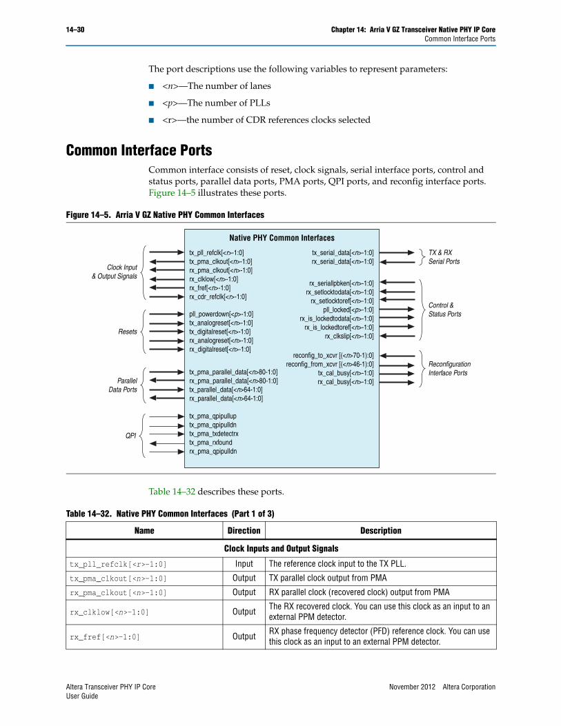
14–30 Chapter 14: Arria V GZ Transceiver Native PHY IP CoreCommon Interface Ports
The port descriptions use the following variables to represent parameters:
■ <n>—The number of lanes
■ <p>—The number of PLLs
■ <r>—the number of CDR references clocks selected
Common Interface PortsCommon interface consists of reset, clock signals, serial interface ports, control and status ports, parallel data ports, PMA ports, QPI ports, and reconfig interface ports. Figure 14–5 illustrates these ports.
Table 14–32 describes these ports.
Figure 14–5. Arria V GZ Native PHY Common Interfaces
tx_pll_refclk[<r>-1:0]tx_pma_clkout[<n>-1:0]rx_pma_clkout[<n>-1:0]rx_clklow[<n>-1:0]rx_fref[<n>-1:0]rx_cdr_refclk[<r>-1:0]
Clock Input& Output Signals
rx_seriallpbken[<n>-1:0]rx_setlocktodata[<n>-1:0]
rx_setlocktoref[<n>-1:0]pll_locked[<p>-1:0]
rx_is_lockedtodata[<n>-1:0]rx_is_lockedtoref[<n>-1:0]
rx_clkslip[<n>-1:0]
Control &Status Portspll_powerdown[<p>-1:0]
tx_analogreset[<n>-1:0]tx_digitalreset[<n>-1:0]rx_analogreset[<n>-1:0]rx_digitalreset[<n>-1:0]
Resets
QPI
tx_pma_parallel_data[<n>80-1:0]rx_pma_parallel_data[<n>80-1:0]tx_parallel_data[<n>64-1:0]rx_parallel_data[<n>64-1:0]
tx_pma_qpipulluptx_pma_qpipulldntx_pma_txdetectrxtx_pma_rxfoundrx_pma_qpipulldn
ParallelData Ports
tx_serial_data[<n>-1:0]rx_serial_data[<n>-1:0]
TX & RXSerial Ports
reconfig_to_xcvr [(<n>70-1):0]reconfig_from_xcvr [(<n>46-1):0]
tx_cal_busy[<n>-1:0]rx_cal_busy[<n>-1:0]
ReconfigurationInterface Ports
Native PHY Common Interfaces
Table 14–32. Native PHY Common Interfaces (Part 1 of 3)
Name Direction Description
Clock Inputs and Output Signals
tx_pll_refclk[<r>-1:0] Input The reference clock input to the TX PLL.
tx_pma_clkout[<n>-1:0] Output TX parallel clock output from PMA
rx_pma_clkout[<n>-1:0] Output RX parallel clock (recovered clock) output from PMA
rx_clklow[<n>-1:0] Output The RX recovered clock. You can use this clock as an input to an external PPM detector.
rx_fref[<n>-1:0] Output RX phase frequency detector (PFD) reference clock. You can use this clock as an input to an external PPM detector.
Altera Transceiver PHY IP Core November 2012 Altera CorporationUser Guide

Chapter 14: Arria V GZ Transceiver Native PHY IP Core 14–31Common Interface Ports
rx_cdr_refclk[<n>-1:0] Input Input reference clock for the RX PFD circuit.
Resets
pll_powerdown[<n>-1:0] Input When asserted, resets the TX PLL. Active high, edge sensitive reset signal.
tx_analogreset[<n>-1:0] Input When asserted, resets for TX PMA, TX clock generation block, and serializer. Active high, edge sensitive reset signal.
tx_digitalreset[<n>-1:0] Input
When asserted, resets the digital components of the TX datapath. Active high, edge sensitive reset signal.If your design includes bonded TX PCS channels, refer to Timing Constraints for Reset Signals when Using Bonded PCS Channels for a SDC constraint you must include in your design.
rx_analogreset[<n>-1:0] Input When asserted, resets the RX CDR, deserializer, Active high, edge sensitive reset signal.
rx_digitalreset[<n>-1:0] Input When asserted, resets the digital components of the RX datapath. Active high, edge sensitive reset signal.
Parallel data ports
tx_pma_parallel_data[<n>80-1:0] InputTX parallel data for the PMA Direct datapath. Driven directly from the FPGA fabric to the PMA. Not used when you enable either the Standard or 10G PCS datapath.
rx_pma_parallel_data[<n>80-1:0] OutputRX PMA parallel data driven from the PMA to the FPGA fabric. Not used when you enable either the Standard or 10G PCS datapath.
tx_parallel_data[<n>64-1:0] Input
PCS TX parallel data. Used when you enable either the Standard or 10G datapath. For the Standard datapath, if you turn on Enable simplified data interface, tx_parallel_data includes only the data and control signals necessary for the current configuration. Dynamic reconfiguration of the interface is not supported.
For the 10G PCS, if the parallel data interface is less than 64 bits wide, the low-order bits of tx_parallel_data are valid.
For the 10G PCS operating in 66:40 mode, the 66 bus is formed as follows: {tx_parallel_data[63:0],tx_10g_control[0],tx_10g_control[1]}.
rx_parallel_data[<n>64-1:0] Output
PCS RX parallel data. Used when you enable either the Standard or 10G datapath. For the Standard datapath, if you turn on Enable simplified data interface, rx_parallel_data includes only the data and control signals necessary for the current configuration. Dynamic reconfiguration of the interface is not supported.
For the 10G PCS, if the parallel data interface is less than 64 bits wide, the low-order bits of rx_parallel_data are valid.
For the 10G PCS operating in 66:40 mode, the 66 bus is formed as follows: {rx_parallel_data[63:0],rx_10g_control[0],rx_10g_control[1]}.
QPI
tx_pma_qpipullup Input QPI control input port. Only for QPI applications.
tx_pma_qpipulldn Input QPI control input port. Only for QPI applications.
Table 14–32. Native PHY Common Interfaces (Part 2 of 3)
Name Direction Description
November 2012 Altera Corporation Altera Transceiver PHY IP CoreUser Guide
14–32 Chapter 14: Arria V GZ Transceiver Native PHY IP CoreCommon Interface Ports
tx_pma_txdetectrx Input
When asserted, the RX detect block in the TX PMA detects the presence of a receiver at the other end of the channel. After receiving a tx_pma_txdetectrx request, the receiver detect block initiates the detection process. Only for QPI applications.
tx_pma_rxfound Output Indicates the status of an RX detection in the TX PMA. Only for QPI applications.
rx_pma_qpipulldn Input QPI control input port. Only for QPI applications.
TX and RX serial ports
tx_serial_data[<n>-1:0] Output TX differential serial output data.
rx_serial_data[<n>-1:0] Input RX differential serial output data.
Control and Status ports
rx_seriallpbken[<n>-1:0] Input When asserted, the transceiver enters loopback mode. Loopback drives TX data to the RX interface.
rx_set_locktodata[<n>-1:0] Input
When asserted, programs the RX CDR to manual lock to data mode in which you control the reset sequence using the rx_setlocktoref and rx_setlocktodata. Refer to Reset Sequence for CDR in Manual Lock Mode inTransceiver Reset Control and Power-Down in Arria V Devices for more information about manual control of the reset sequence.
rx_set_locktoref[<n>-1:0] Input
When asserted, programs the RX CDR to manual lock to reference mode in which you control the reset sequence using the rx_setlocktoref and rx_setlocktodata. Refer to Reset Sequence for CDR in Manual Lock Mode in Transceiver Reset Control and Power-Down in Arria V Devices for more information about manual control of the reset sequence.
pll_locked[<p>-1:0] Output When asserted, indicates that the PLL is locked to the input reference clock.
rx_is_lockedtodata[<n>-1:0] Output When asserted, the CDR is locked to the incoming data.
rx_is_lockedtoref[<n>-1:0] Output When asserted, the CDR is locked to the incoming reference clock.
rx_clkslip[<n>-1:0] Input When asserted, the deserializer slips one clock edge. This signal is used to achieve word alignment.
Reconfig Interface Ports
reconfig_to_xcvr [(<n>70-1):0] InputReconfiguration signals from the Transceiver Reconfiguration Controller. <n> grows linearly with the number of reconfiguration interfaces.
reconfig_from_xcvr [(<n>46-1):0] OutputReconfiguration signals to the Transceiver Reconfiguration Controller. <n> grows linearly with the number of reconfiguration interfaces.
tx_cal_busy[<n>-1:0] Output Reconfiguration status, indicates TX calibration is in progress
rx_cal_busy[<n>-1:0] Output Reconfiguration status, indicates RX calibration is in progress
Table 14–32. Native PHY Common Interfaces (Part 3 of 3)
Name Direction Description
Altera Transceiver PHY IP Core November 2012 Altera CorporationUser Guide
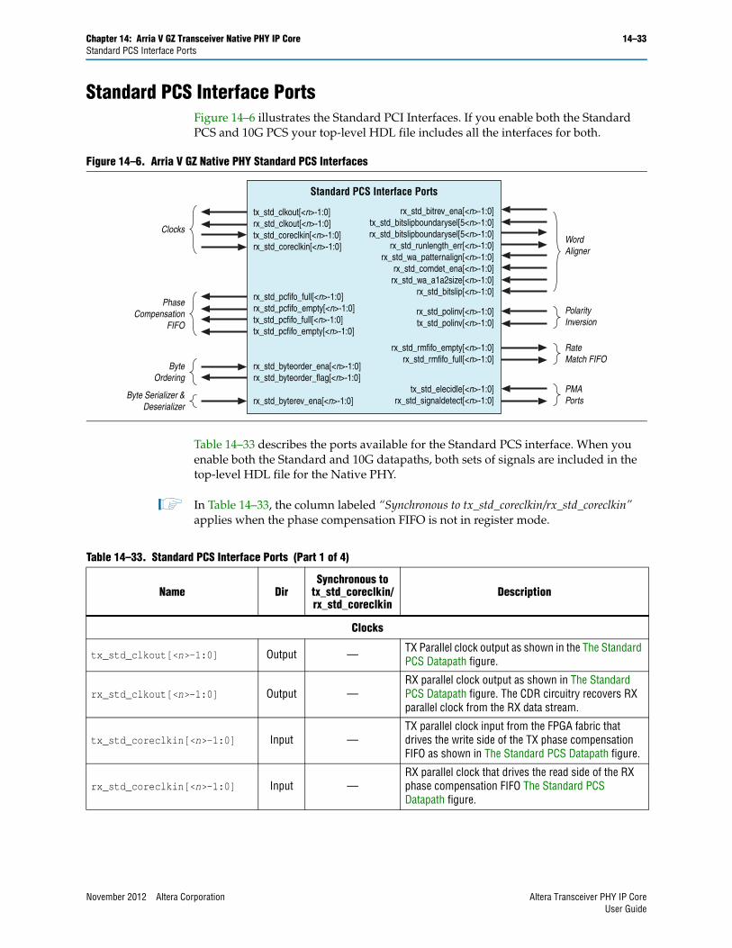
Chapter 14: Arria V GZ Transceiver Native PHY IP Core 14–33Standard PCS Interface Ports
Standard PCS Interface PortsFigure 14–6 illustrates the Standard PCI Interfaces. If you enable both the Standard PCS and 10G PCS your top-level HDL file includes all the interfaces for both.
Table 14–33 describes the ports available for the Standard PCS interface. When you enable both the Standard and 10G datapaths, both sets of signals are included in the top-level HDL file for the Native PHY.
1 In Table 14–33, the column labeled “Synchronous to tx_std_coreclkin/rx_std_coreclkin” applies when the phase compensation FIFO is not in register mode.
Figure 14–6. Arria V GZ Native PHY Standard PCS Interfaces
tx_std_clkout[<n>-1:0] rx_std_clkout[<n>-1:0]tx_std_coreclkin[<n>-1:0]rx_std_coreclkin[<n>-1:0]
ClocksWordAligner
rx_std_pcfifo_full[<n>-1:0] rx_std_pcfifo_empty[<n>-1:0] tx_std_pcfifo_full[<n>-1:0] tx_std_pcfifo_empty[<n>-1:0]
PhaseCompensation
FIFO
rx_std_byteorder_ena[<n>-1:0] rx_std_byteorder_flag[<n>-1:0]
ByteOrdering
rx_std_rmfifo_empty[<n>-1:0]rx_std_rmfifo_full[<n>-1:0]
RateMatch FIFO
rx_std_polinv[<n>-1:0]tx_std_polinv[<n>-1:0]
PolarityInversion
PMAPorts
Standard PCS Interface Ports
rx_std_bitrev_ena[<n>-1:0]tx_std_bitslipboundarysel[5<n>-1:0]rx_std_bitslipboundarysel[5<n>-1:0]
rx_std_runlength_err[<n>-1:0]rx_std_wa_patternalign[<n>-1:0]
rx_std_comdet_ena[<n>-1:0]rx_std_wa_a1a2size[<n>-1:0]
rx_std_bitslip[<n>-1:0]
tx_std_elecidle[<n>-1:0]rx_std_signaldetect[<n>-1:0]rx_std_byterev_ena[<n>-1:0]
Byte Serializer &Deserializer
Table 14–33. Standard PCS Interface Ports (Part 1 of 4)
Name DirSynchronous to
tx_std_coreclkin/rx_std_coreclkin
Description
Clocks
tx_std_clkout[<n>-1:0] Output — TX Parallel clock output as shown in the The Standard PCS Datapath figure.
rx_std_clkout[<n>-1:0] Output —RX parallel clock output as shown in The Standard PCS Datapath figure. The CDR circuitry recovers RX parallel clock from the RX data stream.
tx_std_coreclkin[<n>-1:0] Input —TX parallel clock input from the FPGA fabric that drives the write side of the TX phase compensation FIFO as shown in The Standard PCS Datapath figure.
rx_std_coreclkin[<n>-1:0] Input —RX parallel clock that drives the read side of the RX phase compensation FIFO The Standard PCS Datapath figure.
November 2012 Altera Corporation Altera Transceiver PHY IP CoreUser Guide

14–34 Chapter 14: Arria V GZ Transceiver Native PHY IP CoreStandard PCS Interface Ports
Phase Compensation FIFO
rx_std_pcfifo_full[<n>-1:0] Output YesRX phase compensation FIFO full status flag. Valid when the Phase Compensation FIFO is not in register mode.
rx_std_pcfifo_empty[<n>-1:0] Output YesRX phase compensation FIFO status empty flag. Valid when the Phase Compensation FIFO is not in register mode.
tx_std_pcfifo_full[<n>-1:0] Output YesTX phase compensation FIFO status full flag. Valid when the Phase Compensation FIFO is not in register mode.
tx_std_pcfifo_empty[<n>-1:0] Output YesTX phase compensation FIFO status empty flag. Valid when the Phase Compensation FIFO is not in register mode.
Byte Ordering
rx_std_byteorder_ena[<n>-1:0]
Input No
Byte ordering enable. When this signal is asserted, the byte ordering block initiates a byte ordering operation if the Byte ordering control mode is set to manual. Once byte ordering has occurred, you must deassert and reassert this signal to perform another byte ordering operation. This signal is an synchronous input signal; however, it must be asserted for at least 1 cycle of rx_std_clkout.
rx_std_byteorder_flag[<n>-1:0]
Output Yes
Byte ordering status flag. When asserted, indicates that the byte ordering block has performed a byte order operation. This signal is asserted on the clock cycle in which byte ordering occurred. This signal is synchronous to the rx_std_clkout clock. You must a synchronizer this signal.
Byte Serializer and Deserializer
rx_std_byterev_ena[<n>-1:0] Input NoThis control signals is available in when the PMA width is 16 or 20 bits. When asserted, enables byte reversal on the RX interface.
8B/10B
rx_std_polinv[<n>-1:0] Input No
Polarity inversion for the 8B/10B decoder, When set, the RX channels invert the polarity of the received data. You can use this signal to correct the polarity of differential pairs if the transmission circuitry or board layout mistakenly swapped the positive and negative signals. The polarity inversion function operates on the word aligner input.
tx_std_polinv[<n>-1:0] Input No Polarity inversion, part of 8B10B encoder, When set, the TX interface inverts the polarity of the TX data.
Table 14–33. Standard PCS Interface Ports (Part 2 of 4)
Name DirSynchronous to
tx_std_coreclkin/rx_std_coreclkin
Description
Altera Transceiver PHY IP Core November 2012 Altera CorporationUser Guide
Chapter 14: Arria V GZ Transceiver Native PHY IP Core 14–35Standard PCS Interface Ports
Rate Match FIFO
rx_std_rm_fifo_empty[<n>-1:0]
Output NoRate match FIFO empty flag. When asserted, the rate match FIFO is empty. You must synchronize this signal.
rx_std_rm_fifo_full[<n>-1:0] Output No Rate match FIFO full flag. When asserted the rate match FIFO is full. You must synchronize this signal.
Word Aligner
rx_std_bitrev_ena[<n>-1:0] Input No
When asserted, enables bit reversal on the RX interface. Bit order may be reversed if external transmission circuitry transmits the most significant bit first. When enabled, the receive circuitry receives all words in the reverse order. The bit reversal circuitry operates on the output of the word aligner.
tx_std_bitslipboundarysel[5<n>-1:0]
Input No Bit-Slip boundary selection signal. Specifies the number of bits that the TX bit slipper must slip.
rx_std_bitslipboundarysel[5<n>-1:0]
Output No
This signal operates when the word aligner is in bit-slip word alignment mode. It reports the number of bits that the RX block slipped to achieve deterministic latency.
rx_std_runlength_err[<n>-1:0]
Output No
When asserted, indicates a run length violation. Asserted if the number of consecutive 1s or 0s exceeds the number specified in th0e parameter editor GUI.
rx_st_wa_patternalign Input No Asserted to enable word alignment in manual word alignment mode.
rx_std_wa_a1a2size[<n>-1:0] Input No
Used for the SONET protocol. Asserted when the A1 and A2 framing bytes must be detected. A1 and A2 are SONET backplane bytes and are only used when the PMA data width is 8 bits.
rx_std_bitslip[<n>-1:0] Input No
Used when word aligner mode is bit-slip mode. For every rising edge of the rx_std_bitslip signal, the word boundary is shifted by 1 bit. Each bitslip removes the earliest received bit from the received data. You must synchronize this signal.
Table 14–33. Standard PCS Interface Ports (Part 3 of 4)
Name DirSynchronous to
tx_std_coreclkin/rx_std_coreclkin
Description
November 2012 Altera Corporation Altera Transceiver PHY IP CoreUser Guide
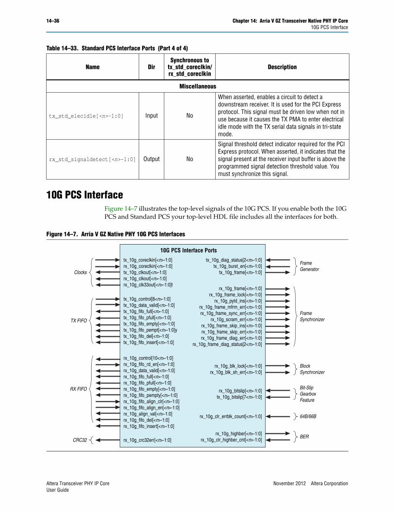
14–36 Chapter 14: Arria V GZ Transceiver Native PHY IP Core10G PCS Interface
10G PCS InterfaceFigure 14–7 illustrates the top-level signals of the 10G PCS. If you enable both the 10G PCS and Standard PCS your top-level HDL file includes all the interfaces for both.
Miscellaneous
tx_std_elecidle[<n>-1:0] Input No
When asserted, enables a circuit to detect a downstream receiver. It is used for the PCI Express protocol. This signal must be driven low when not in use because it causes the TX PMA to enter electrical idle mode with the TX serial data signals in tri-state mode.
rx_std_signaldetect[<n>-1:0] Output No
Signal threshold detect indicator required for the PCI Express protocol. When asserted, it indicates that the signal present at the receiver input buffer is above the programmed signal detection threshold value. You must synchronize this signal.
Table 14–33. Standard PCS Interface Ports (Part 4 of 4)
Name DirSynchronous to
tx_std_coreclkin/rx_std_coreclkin
Description
Figure 14–7. Arria V GZ Native PHY 10G PCS Interfaces
Clocks
FrameGenerator
TX FIFO
RX FIFO
BlockSynchronizer
FrameSynchronizer
Bit-SlipGearboxFeature
64B/66B
BER
10G PCS Interface Ports
CRC32
tx_10g_coreclkin[<n>-1:0]rx_10g_coreclkin[<n>-1:0]tx_10g_clkout[<n>-1:0]rx_10g_clkout[<n>-1:0]rx_10g_clk33out[<n>-1:0]t
tx_10g_control[8<n>-1:0]tx_10g_data_valid[<n>-1:0]tx_10g_fifo_full[<n>-1:0]tx_10g_fifo_pfull[<n>-1:0]tx_10g_fifo_empty[<n>-1:0]tx_10g_fifo_pempt[<n>-1:0]ytx_10g_fifo_del[<n>-1:0]tx_10g_fifo_insert[<n>-1:0]
rx_10g_control[10<n>-1:0]rx_10g_fifo_rd_en[<n>-1:0]rx_10g_data_valid[<n>-1:0]rx_10g_fifo_full[<n>-1:0]rx_10g_fifo_pfull[<n>-1:0]rx_10g_fifo_empty[<n>-1:0]rx_10g_fifo_pempty[<n>-1:0]rx_10g_fifo_align_clr[<n>-1:0]rx_10g_fifo_align_en[<n>-1:0]rx_10g_align_val[<n>-1:0]rx_10g_fifo_del[<n>-1:0]rx_10g_fifo_insert[<n>-1:0]
rx_10g_crc32err[<n>-1:0]
tx_10g_diag_status[2<n>-1:0]tx_10g_burst_en[<n>-1:0]
tx_10g_frame[<n>-1:0]
rx_10g_frame[<n>-1:0]rx_10g_frame_lock[<n>-1:0]
rx_10g_pyld_ins[<n>-1:0]rx_10g_frame_mfrm_err[<n>-1:0]rx_10g_frame_sync_err[<n>-1:0]
rx_10g_scram_err[<n>-1:0]rx_10g_frame_skip_ins[<n>-1:0]rx_10g_frame_skip_err[<n>-1:0]rx_10g_frame_diag_err[<n>-1:0]
rx_10g_frame_diag_status[2<n>-1:0]
rx_10g_blk_lock[<n>-1:0]rx_10g_blk_sh_err[<n>-1:0]
rx_10g_bitslip[<n>-1:0]tx_10g_bitslip[7<n>-1:0]
rx_10g_clr_errblk_count[<n>-1:0]
rx_10g_highber[<n>-1:0]rx_10g_clr_highber_cnt[<n>-1:0]
Altera Transceiver PHY IP Core November 2012 Altera CorporationUser Guide

Chapter 14: Arria V GZ Transceiver Native PHY IP Core 14–3710G PCS Interface
Table 14–34 describes the signals available for the 10G PCS datapath. When you enable both the 10G and Standard datapaths, both sets of signals are included in the top-level HDL file for the Native PHY.
1 In Table 14–34, the column labeled “Synchronous to tx_10_coreclkin/rx_10g_coreclkin” refers to cases where the phase compensation FIFO is not in register mode.
,
Table 14–34. 10G PCS Interface Ports (Part 1 of 8)
Name DirSynchronous to
tx_10g_coreclkin/rx_10g_coreclkin
Description
Clocks
tx_10g_coreclkin[<n>-1:0] Input — TX parallel clock input that drive the write side of the TX FIFO as shown in The 10G PCS datapath figure.
rx_10g_coreclkin[<n>-1:0] Input — RX parallel clock input that drives the read side of the RX FIFO as shown in The 10G PCS datapath figure.
tx_10g_clkout[<n>-1:0] Output — TX parallel clock output for the TX PCS as shown in The 10G PCS datapath figure.
rx_10g_clkout[<n>-1:0] Output — RX parallel clock output which is recovered from the RX data stream as shown in The 10G PCS datapath figure.
rx_10g_clk33out[<n>-1:0] Output — A divide by 33 clock output. You typically need this option when the fabric to PCS interface width is 66 bits.
TX FIFO
tx_10g_control[9<n>-1:0] Input Yes
TX control signals for the Interlaken, 10GBASE-R, and Basic protocols. Synchronous to tx_10g_coreclk_in. The following signals are defined:
Interlaken mode:
■ [8]: Active-high synchronous error insertion control bit
■ [7:3]: Not Used
■ [2]: Inversion signal, must always be set to 1'b0.
■ [1]: Sync Header, 1 indicates a control word
■ [0]: Sync Header, 1 indicates a data word
10G BaseR mode:
■ [8]: Active-high synchronous error insertion control signal
■ [7]: MII control signal for tx_data[63:56]
■ [6]: MII control signal for tx_data[55:48]
■ [5]: MII control signal for tx_data[47:40]
■ [4]: MII control signal for tx_data[39:32]
■ [3]: MII control signal for tx_data[31:24]
■ [2]: MII control signal for tx_data[23:16]
■ [1]: MII control signal for tx_data[15:8]
■ [0]: MII control signal for tx_data[7:0]
November 2012 Altera Corporation Altera Transceiver PHY IP CoreUser Guide
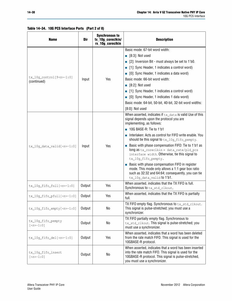
14–38 Chapter 14: Arria V GZ Transceiver Native PHY IP Core10G PCS Interface
tx_10g_control[9<n>-1:0](continued) Input Yes
Basic mode: 67-bit word width:
■ [8:3]: Not used
■ [2]: Inversion Bit - must always be set to 1'b0.
■ [1]: Sync Header, 1 indicates a control word)
■ [0]: Sync Header, 1 indicates a data word)
Basic mode: 66-bit word width:
■ [8:2]: Not used
■ [1]: Sync Header, 1 indicates a control word)
■ [0]: Sync Header, 1 indicates 1 data word)
Basic mode: 64-bit, 50-bit, 40-bit, 32-bit word widths:
[8:0]: Not used
tx_10g_data_valid[<n>-1:0] Input Yes
When asserted, indicates if tx_data is valid Use of this signal depends upon the protocol you are implementing, as follows:
■ 10G BASE-R: Tie to 1'b1
■ Interlaken: Acts as control for FIFO write enable. You should tie this signal to tx_10g_fifo_pempty.
■ Basic with phase compensation FIFO: Tie to 1'b1 as long as tx_coreclkin = data_rate/pld_pcs interface width. Otherwise, tie this signal to tx_10g_fifo_pempty.
■ Basic with phase compensation FIFO in register mode. This mode only allows a 1:1 gear box ratio such as 32:32 and 64:64; consequently, you can tie tx_10g_data_valid to 1’b1.
tx_10g_fifo_full[<n>-1:0] Output Yes When asserted, indicates that the TX FIFO is full. Synchronous to tx_std_clkout,
tx_10g_fifo_pfull[<n>-1:0] Output Yes When asserted, indicates that the TX FIFO is partially full.
tx_10g_fifo_empty[<n>-1:0] Output NoTX FIFO empty flag. Synchronous to tx_std_clkout. This signal is pulse-stretched; you must use a synchronizer.
tx_10g_fifo_pempty[<n>-1:0]
Output NoTX FIFO partially empty flag. Synchronous to tx_std_clkout. This signal is pulse-stretched; you must use a synchronizer.
tx_10g_fifo_del[<n>-1:0] Output YesWhen asserted, indicates that a word has been deleted from the rate match FIFO. This signal is used for the 10GBASE-R protocol.
tx_10g_fifo_insert[<n>-1:0]
Output No
When asserted, indicates that a word has been inserted into the rate match FIFO. This signal is used for the 10GBASE-R protocol. This signal is pulse-stretched, you must use a synchronizer.
Table 14–34. 10G PCS Interface Ports (Part 2 of 8)
Name DirSynchronous to
tx_10g_coreclkin/rx_10g_coreclkin
Description
Altera Transceiver PHY IP Core November 2012 Altera CorporationUser Guide
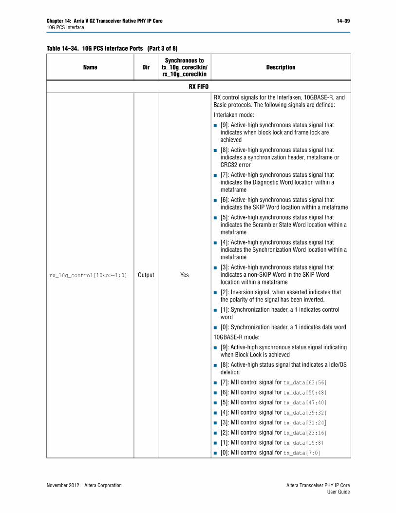
Chapter 14: Arria V GZ Transceiver Native PHY IP Core 14–3910G PCS Interface
RX FIFO
rx_10g_control[10<n>-1:0] Output Yes
RX control signals for the Interlaken, 10GBASE-R, and Basic protocols. The following signals are defined:
Interlaken mode:
■ [9]: Active-high synchronous status signal that indicates when block lock and frame lock are achieved
■ [8]: Active-high synchronous status signal that indicates a synchronization header, metaframe or CRC32 error
■ [7]: Active-high synchronous status signal that indicates the Diagnostic Word location within a metaframe
■ [6]: Active-high synchronous status signal that indicates the SKIP Word location within a metaframe
■ [5]: Active-high synchronous status signal that indicates the Scrambler State Word location within a metaframe
■ [4]: Active-high synchronous status signal that indicates the Synchronization Word location within a metaframe
■ [3]: Active-high synchronous status signal that indicates a non-SKIP Word in the SKIP Word location within a metaframe
■ [2]: Inversion signal, when asserted indicates that the polarity of the signal has been inverted.
■ [1]: Synchronization header, a 1 indicates control word
■ [0]: Synchronization header, a 1 indicates data word
10GBASE-R mode:
■ [9]: Active-high synchronous status signal indicating when Block Lock is achieved
■ [8]: Active-high status signal that indicates a Idle/OS deletion
■ [7]: MII control signal for tx_data[63:56]
■ [6]: MII control signal for tx_data[55:48]
■ [5]: MII control signal for tx_data[47:40]
■ [4]: MII control signal for tx_data[39:32]
■ [3]: MII control signal for tx_data[31:24]
■ [2]: MII control signal for tx_data[23:16]
■ [1]: MII control signal for tx_data[15:8]
■ [0]: MII control signal for tx_data[7:0]
Table 14–34. 10G PCS Interface Ports (Part 3 of 8)
Name DirSynchronous to
tx_10g_coreclkin/rx_10g_coreclkin
Description
November 2012 Altera Corporation Altera Transceiver PHY IP CoreUser Guide

14–40 Chapter 14: Arria V GZ Transceiver Native PHY IP Core10G PCS Interface
rx_10g_control[10<n>-1:0]
(continued)Output Yes
Basic mode: 67-bit mode with Block Sync:
■ [9]: Active-high synchronous status signal that indicates when Block Lock is achieved.
■ [8]: Active-high synchronous status signal that indicates a sync header error
■ [7:3]: Not used [2]: Used
■ [1]: Synchronization header, a 1 indicates control word
■ [0]: Synchronization header, a 1 indicates data word
Basic mode: 66-bit mode with Block Sync:
[9]: Active-high synchronous status signal that indicates when Block Lock is achieved.
[8]: Active-high synchronous status signal that indicates a sync header error.
[7:2]: Not used
■ [1]: Synchronization header, a 1 indicates control word
■ [0]: Synchronization header, a 1 indicates data word
Basic mode: 67-bit mode without Block Sync:
[9:3]: Not used
66-bit mode without Block Sync:
[9:2]: Not used
■ [1]: Synchronization header, a 1 indicates control word
■ [0]: Synchronization header, a 1 indicates data word
Basic mode: 64-bit, 50-bit, 40-bit and 32-bit modes:
[9:0]: Not used
rx_10g_fifo_rd_en[<n>-1:0] Input Yes Active high read enable signal for RX FIFO. Asserting this signal reads 1 word from the RX FIFO.
rx_10g_data_valid[<n>-1:0] Output Yes
Active valid data signal with the following use:
■ 10GBASE-R: Always high
■ Interlaken: Toggles indicating when rx_data is valid.
■ Basic - Phase compensation: Toggles indicating when rx_data is valid.
■ Basic - Register: Toggles indicating when rx_data is valid.
rx_10g_fifo_full[<n>-1:0] Output NoActive high RX FIFO full flag. Synchronous to rx_10g_clkout. This signal is pulse-stretched; you must use a synchronizer.
Table 14–34. 10G PCS Interface Ports (Part 4 of 8)
Name DirSynchronous to
tx_10g_coreclkin/rx_10g_coreclkin
Description
Altera Transceiver PHY IP Core November 2012 Altera CorporationUser Guide

Chapter 14: Arria V GZ Transceiver Native PHY IP Core 14–4110G PCS Interface
rx_10g_fifo_pfull[<n>-1:0] Output NoRX FIFO partially full flag.Synchronous to rx_10g_clkout. This signal is pulse-stretched; you must use a synchronizer.
rx_10g_fifo_empty[<n>-1:0] Output Yes Active high RX FIFO empty flag,
rx_10g_fifo_pempty[<n>-1:0]
Output Yes Active high. RX FIFO partially empty flag,
rx_10g_fifo_align_clr[<n>-1:0]
Input Yes
For the Interlaken protocol, this signal clears the current word alignment when the RX FIFO acts as a deskew FIFO. When it is asserted, the RX FIFO is reset and searches for a new alignment pattern.
rx_10g_fifo_align_en[<n>-1:0]
Input Yes For the Interlaken protocol, you must assert this signal to enable the RX FIFO for alignment.
rx_10g_align_val[<n>-1:0] Output Yes For the Interlaken protocol, an active high indication that the alignment pattern has been found
Rx_10g_fifo_del[<n>-1:0] Output No
When asserted, indicates that a word has been deleted from the TX FIFO. This signal is used for the 10GBASE-R protocol. This signal is pulse-stretched; you must use a synchronizer.
Rx_10g_fifo_insert[<n>-1:0]
Output Yes
Active-high 10G BaseR RX FIFO insertion flag
When asserted, indicates that a word has been inserted into the TX FIFO. This signal is used for the 10GBASE-R protocol.
CRC32
rx_10g_crc32err[<n>-1:0] Output No
For the Interlaken protocol, asserted to indicate that the CRC32 Checker has found a CRC32 error in the current metaframe. Is is asserted at the end of current metaframe. This signal is pulse-stretched; you must use a synchronizer.
Frame Generator
tx_10g_diag_status[2<n>-1:0]
Input No
For the Interlaken protocol, provides diagnostic status information reflecting the lane status message contained in the Framing Layer Diagnostic Word (bits[33:32]). This message is inserted into the next Diagnostic Word generated by the Frame Generation Block. The message must be held static for 5 cycles before and 5 cycles after the tx_frame pulse.
tx_10g_burst_en[<n>-1:0] Input No
For the Interlaken protocol, controls frame generator reads from the TX FIFO. Latched once at the beginning of each metaframe.When 0, the frame generator inserts SKIPs. When 1, the frame generator reads data from the TX FIFO. Must be held static for 5 cycles before and 5 cycles after the tx_frame pulse.
Table 14–34. 10G PCS Interface Ports (Part 5 of 8)
Name DirSynchronous to
tx_10g_coreclkin/rx_10g_coreclkin
Description
November 2012 Altera Corporation Altera Transceiver PHY IP CoreUser Guide
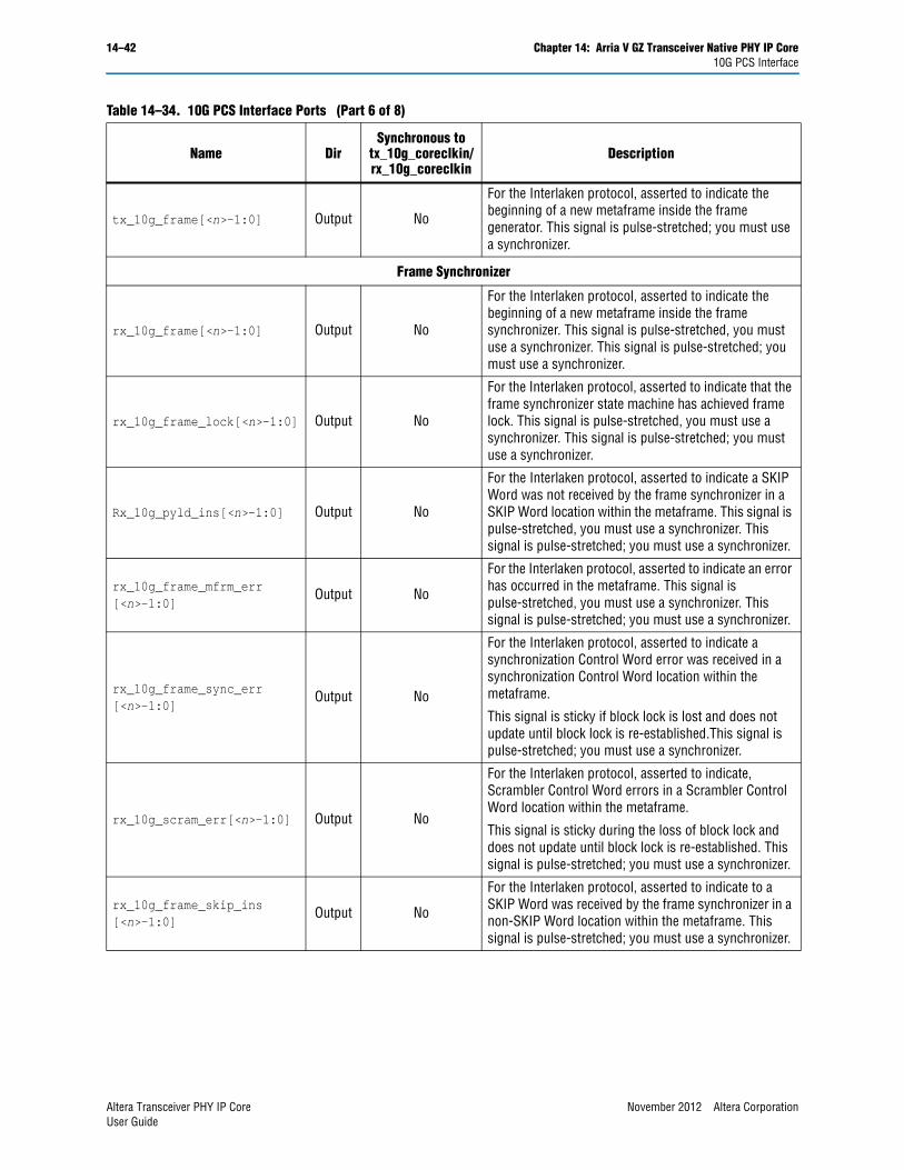
14–42 Chapter 14: Arria V GZ Transceiver Native PHY IP Core10G PCS Interface
tx_10g_frame[<n>-1:0] Output No
For the Interlaken protocol, asserted to indicate the beginning of a new metaframe inside the frame generator. This signal is pulse-stretched; you must use a synchronizer.
Frame Synchronizer
rx_10g_frame[<n>-1:0] Output No
For the Interlaken protocol, asserted to indicate the beginning of a new metaframe inside the frame synchronizer. This signal is pulse-stretched, you must use a synchronizer. This signal is pulse-stretched; you must use a synchronizer.
rx_10g_frame_lock[<n>-1:0] Output No
For the Interlaken protocol, asserted to indicate that the frame synchronizer state machine has achieved frame lock. This signal is pulse-stretched, you must use a synchronizer. This signal is pulse-stretched; you must use a synchronizer.
Rx_10g_pyld_ins[<n>-1:0] Output No
For the Interlaken protocol, asserted to indicate a SKIP Word was not received by the frame synchronizer in a SKIP Word location within the metaframe. This signal is pulse-stretched, you must use a synchronizer. This signal is pulse-stretched; you must use a synchronizer.
rx_10g_frame_mfrm_err[<n>-1:0]
Output No
For the Interlaken protocol, asserted to indicate an error has occurred in the metaframe. This signal is pulse-stretched, you must use a synchronizer. This signal is pulse-stretched; you must use a synchronizer.
rx_10g_frame_sync_err[<n>-1:0]
Output No
For the Interlaken protocol, asserted to indicate a synchronization Control Word error was received in a synchronization Control Word location within the metaframe.
This signal is sticky if block lock is lost and does not update until block lock is re-established.This signal is pulse-stretched; you must use a synchronizer.
rx_10g_scram_err[<n>-1:0] Output No
For the Interlaken protocol, asserted to indicate, Scrambler Control Word errors in a Scrambler Control Word location within the metaframe.
This signal is sticky during the loss of block lock and does not update until block lock is re-established. This signal is pulse-stretched; you must use a synchronizer.
rx_10g_frame_skip_ins[<n>-1:0]
Output No
For the Interlaken protocol, asserted to indicate to a SKIP Word was received by the frame synchronizer in a non-SKIP Word location within the metaframe. This signal is pulse-stretched; you must use a synchronizer.
Table 14–34. 10G PCS Interface Ports (Part 6 of 8)
Name DirSynchronous to
tx_10g_coreclkin/rx_10g_coreclkin
Description
Altera Transceiver PHY IP Core November 2012 Altera CorporationUser Guide

Chapter 14: Arria V GZ Transceiver Native PHY IP Core 14–4310G PCS Interface
rx_10g_frame_skip_err[<n>-1:0]
Output No
For the Interlaken protocol, asserted to indicate a Skip Control Word error was received in a Skip Control Word location within the metaframe.
This signal is sticky during the loss of block lock and does not update until block lock is re-established. This signal is pulse-stretched; you must use a synchronizer.
rx_10g_frame_diag_err[<n>-1:0]
Output No
For the Interlaken protocol, asserted to indicate a Diagnostic Control Word error was received in a Diagnostic Control Word location within the metaframe.
This signal is sticky during the loss of block lock and does not update until block lock is re-established. This signal is pulse-stretched; you must use a synchronizer.
rx_10g_fram_diag_status[2<n>-1:0]
outputs No
For the Interlaken protocol, reflects the lane status message contained in the framing layer Diagnostic Word (bits[33:32]). This information is latched when a valid Diagnostic Word is received in a Diagnostic Word Metaframe location. This signal is pulse-stretched; you must use a synchronizer.
Block Synchronizer
rx_10g_blk_lock[<n>-1:0] Output No
Active-high status signal that is asserted when block synchronizer acquires block lock. Valid for the 10GBASE-R and Interlaken protocols, and any basic mode that uses the lock state machine to achieve and monitor block synchronization for word alignment. Once the block synchronizer acquires block lock, it takes at least 16 errors for rx_10g_blk_lock to be deasserted.
rx_10g_blk_sh_err[<n>-1:0] Output No
Error status signal from block synchronizer indicating an invalid synchronization header has been received. Valid for the 10GBASE-R and Interlaken protocols, and any legal basic mode that uses the lock state machine to achieve and monitor block synchronization for word alignment. Active only after block lock is achieved. This signal is pulse-stretched; you must use a synchronizer.
Bit-Slip Gearbox Feature
rx_10g_bitslip[<n>-1:0] Input No User control bit-slip in the RX Gearbox. Slips one bit per rising edge pulse.
tx_10g_bitslip[7<n>-1:0] Input NoTX bit-slip is controlled by tx_bitslip port. s
Shifts the number of bit location specified by tx_bitslip. The maximum shift is <pcswidth-1>.
64b/66b
rx_10g_clr_errblk_count[<n>-1:0]
Input NoFor the 10GBASE-R protocol, asserted to clear the error block counter which counts the number of times the RX state machine enters the RX error state.
Table 14–34. 10G PCS Interface Ports (Part 7 of 8)
Name DirSynchronous to
tx_10g_coreclkin/rx_10g_coreclkin
Description
November 2012 Altera Corporation Altera Transceiver PHY IP CoreUser Guide

14–44 Chapter 14: Arria V GZ Transceiver Native PHY IP CoreSDC Timing Constraints
SDC Timing Constraints The Quartus II 12.1 software reports timing violations for asynchronous inputs to the Standard PCS and 10G PCS. Because many violations are for asynchronous paths, they do not represent actual timing failures. You may choose one of the following three approaches to identify these false timing paths to the Quartus II or TimeQuest software.
■ You can cut these paths in your Synopsys Design Constraints (.sdc) file by using the set_false_path command as shown in Example 14–1.
BER
rx_10g_highber[<n>-1:0] Output No
For the 10GBASE-R protocol, status signal asserted to indicate a bit error ratio of >10–4. A count of 16 in 125us indicates a bit error ratio of >10–4. Once asserted, it remains high for at least 125 s.
rx_10g_clr_highber_cnt[<n>-1:0]
Input No
For the 10GBASE-R protocol, status signal asserted to clear the BER counter which counts the number of times the BER state machine enters the BER_BAD_SH state. This signal has no effect on the operation of the BER state machine.
Table 14–34. 10G PCS Interface Ports (Part 8 of 8)
Name DirSynchronous to
tx_10g_coreclkin/rx_10g_coreclkin
Description
Example 14–1. Using the set_false_path Constraint to Identify Asynchronous Inputs
set_false_path -through {*10gtxbursten*} -to [get_registers *10g_tx_pcs*SYNC_DATA_REG*]set_false_path -through {*10gtxdiagstatus*} -to [get_registers *10g_tx_pcs*SYNC_DATA_REG*]set_false_path -through {*10gtxwordslip*} -to [get_registers *10g_tx_pcs*SYNC_DATA_REG*]set_false_path -through {*10gtxbitslip*} -to [get_registers *10g_tx_pcs*SYNC_DATA_REG*]set_false_path -through {*10grxbitslip*} -to [get_registers *10g_rx_pcs*SYNC_DATA_REG*]set_false_path -through {*10grxclrbercount*} -to [get_registers *10g_rx_pcs*SYNC_DATA_REG*] set_false_path -through {*10grxclrerrblkcnt*} -to [get_registers *10g_rx_pcs*SYNC_DATA_REG*] set_false_path -through {*10grxprbserrclr*} -to [get_registers *10g_rx_pcs*SYNC_DATA_REG*]
set_false_path -through {*8gbitslip*} -to [get_registers *8g_rx_pcs*SYNC_DATA_REG*]set_false_path -through {*8gbytordpld*} -to [get_registers *8g_rx_pcs*SYNC_DATA_REG*] set_false_path -through {*8gcmpfifoburst*} -to [get_registers *8g_rx_pcs*SYNC_DATA_REG*] set_false_path -through {*8gphfifoburstrx*} -to [get_registers *8g_rx_pcs*SYNC_DATA_REG*]
set_false_path -through {*8gsyncsmen*} -to [get_registers *8g*pcs*SYNC_DATA_REG*]set_false_path -through {*8gwrdisablerx*} -to [get_registers *8g_rx_pcs*SYNC_DATA_REG*] set_false_path -through {*rxpolarity*} -to [get_registers *SYNC_DATA_REG*]set_false_path -through {*pldeidleinfersel*} -to [get_registers *SYNC_DATA_REG*]
Altera Transceiver PHY IP Core November 2012 Altera CorporationUser Guide

Chapter 14: Arria V GZ Transceiver Native PHY IP Core 14–45Dynamic Reconfiguration
■ You can use the set_max_delay constraint on a given path to create a constraint for asynchronous signals that do not have a specific clock relationship but require a maximum path delay. Example 14–2 illustrates this approach.
■ You can use the set_false path command only during Timequest timing analysis. Example 14–3 illustrates this approach.
1 In in all of these examples, you must substitute you actual signal names for the signal names shown.
Dynamic Reconfiguration As silicon progresses towards smaller process nodes, circuit performance is affected more by variations due to process, voltage, and temperature (PVT). These process variations result in analog voltages that can be offset from required ranges. The calibration performed by the dynamic reconfiguration interface compensates for variations due to PVT.
For non-bonded clocks, each channel and each TX PLL has a separate dynamic reconfiguration interfaces. The MegaWizard Plug-In Manager provides informational messages on the connectivity of these interfaces. Example 14–4 shows the messages for the Arria V GZ Native PHY with four duplex channels, four TX PLLs, in a non-bonded configuration.
For more information about transceiver reconfiguration refer to Chapter 16, Transceiver Reconfiguration Controller IP Core.
If you are using ×6 or ×N bonding, transceiver dynamic reconfiguration requires that you assign the starting channel number. Logical channel 0 should be assigned to either physical transceiver channel 1 or channel 4 of a transceiver bank. However, if you have already created a PCB with a different lane assignment for logical lane 0, you can use the workaound shown in Example 14–5 to remove this restriction. Example 14–5 redefines the pma_bonding_master parameter using the Quartus II
Example 14–2. Using the mandala Constraint to Identify Asynchronous Inputs
# Example: Apply 10ns max delayset_max_delay -from *tx_from_fifo* -to *8g*pcs*SYNC_DATA_REG1 10
Example 14–3. Using the set_false TimeQuest Constraint to Identify Asynchronous Inputs
#if {$::TimeQuestInfo(nameofexecutable) eq "quartus_fit"} { #} else {#set_false_path -from [get_registers {*tx_from_fifo*}] -through {*txbursten*} -to [get_registers *8g_*_pcs*SYNC_DATA_REG
Example 14–4. Informational Messages for the Transceiver Reconfiguration Interface
PHY IP will require 8 reconfiguration interfaces for connection to the external reconfiguration controller.Reconfiguration interface offsets 0-3 are connected to the transceiver channels.Reconfiguration interface offsets 4–7 are connected to the transmit PLLs.
November 2012 Altera Corporation Altera Transceiver PHY IP CoreUser Guide
14–46 Chapter 14: Arria V GZ Transceiver Native PHY IP CoreSimulation Support
Assignment Editor. In this example, the pma_bonding_master was originally assigned to physical channel 1. (The original assignment could also have been to physical channel 4.) The to parameter reassigns the pma_bonding_master to the Deterministic Latency PHY instance name. You must substitute the instance name from your design for the instance name shown in quotation marks
Simulation SupportThe Quartus II 12.1 release provides simulation and compilation support for the Arria V GZ Native PHY IP Core. Refer to Running a Simulation Testbench for a description of the directories and files that the Quartus II software creates automatically when you generate your Arria V GZ Transceiver Native PHY IP Core.
Example 14–5. Overriding Logical Channel 0 Channel Assignment Restrictions in Arria V GZ Device for ×6 or ×N Bonding
set_parameter -name pma_bonding_master "\"1\"" -to "<PHY IP instance name>"
Altera Transceiver PHY IP Core November 2012 Altera CorporationUser Guide

November 2012 Altera Corporation
15. Cyclone V Transceiver Native PHY IPCore
The Cyclone V Transceiver Native PHY IP Core provides direct access to all control and status signals of the transceiver channels. Unlike other PHY IP Cores, the Native PHY IP Core does not include an Avalon Memory-Mapped (Avalon-MM) interface. Instead, it exposes all signals directly as ports. The Cyclone V Transceiver Native PHY IP Core includes the Standard PCS. You can select the PCS functions and control and status port that your transceiver PHY requires.
The Native Transceiver PHY does not include an embedded reset controller. You can either design custom reset logic or incorporate Altera’s “Transceiver PHY Reset Controller IP Core” to implement reset functionality. Figure 15–1 illustrates the use of the Cyclone V Transceiver Native PHY IP Core. As this figure illustrates, TX PLL and clock data recovery (CDR) reference clocks from the pins of the device are input to the PLL module and CDR logic. The Standard PCS drives TX parallel data and receives RX parallel data.
In a typical design, the separately instantiated Transceiver PHY Reset Controller drives reset signals to Native PHY and receives calibration and locked status signal from the Native PHY. The Native PHY reconfiguration buses connect the external Transceiver Reconfiguration Controller for calibration and dynamic reconfiguration of the channel and PLLs.
You specify the initial configuration when you parameterize the IP core. The Transceiver Native PHY IP Core connects to the “Transceiver Reconfiguration Controller IP Core” to dynamically change reference clocks, PLL connectivity, and the channel configurations at runtime.
Figure 15–1. Cyclone Native Transceiver PHY IP Core
PLLsPMA
altera_xcvr_native_cv Transceiver Native PHY
RX PCS Parallel Data
TX PCS Parallel Data
CDR Reference Clock
TX PLL Reference Clock
CDR
RX Serial Data
to FPGA fabric
TransceiverReconfiguration
Controller
Reconfiguration to XCVR
Reconfiguration from XCVR
TX and RX Resets
Calilbration Busy
PLL and RX Locked
TransceiverPHY ResetController
TX Serial DataSerializer
De-Serializer
StandardPCS
Altera Transceiver PHY IP CoreUser Guide
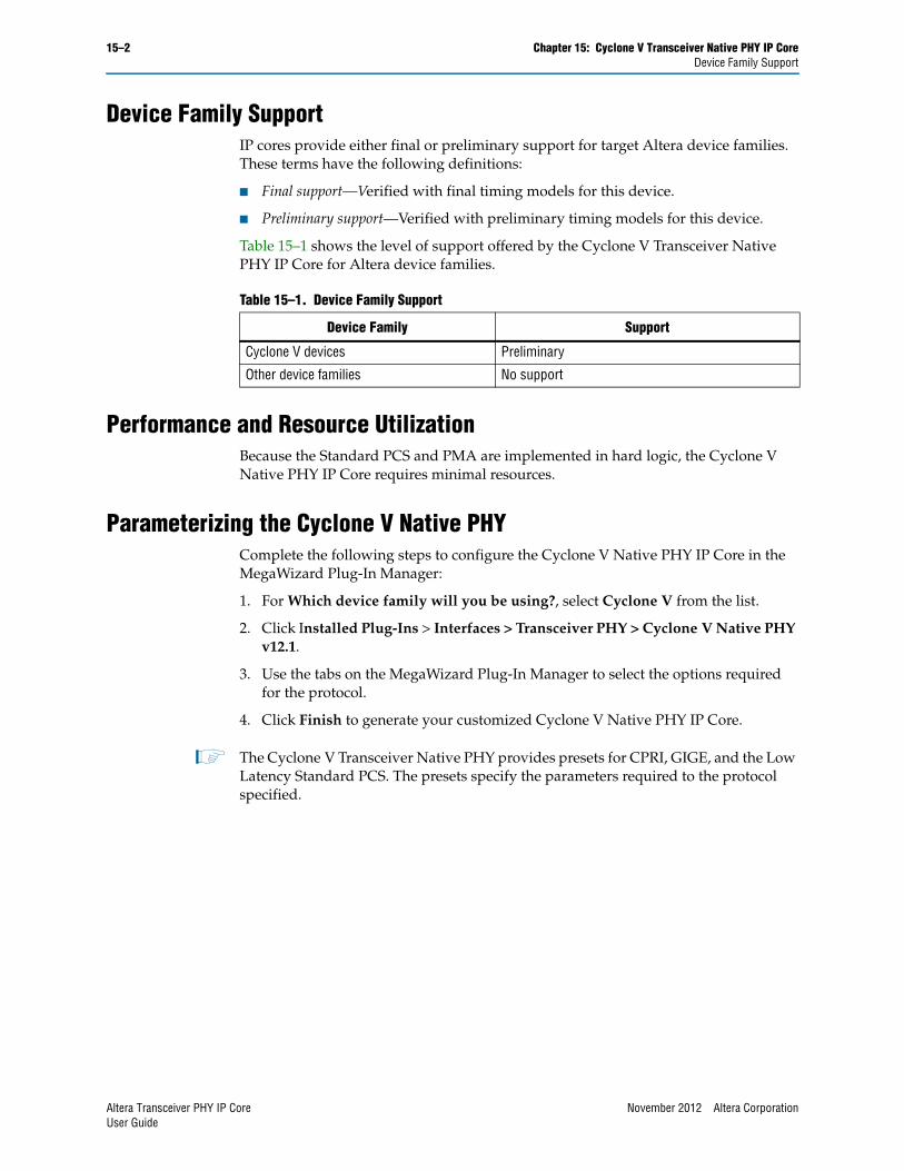
15–2 Chapter 15: Cyclone V Transceiver Native PHY IP CoreDevice Family Support
Device Family SupportIP cores provide either final or preliminary support for target Altera device families. These terms have the following definitions:
■ Final support—Verified with final timing models for this device.
■ Preliminary support—Verified with preliminary timing models for this device.
Table 15–1 shows the level of support offered by the Cyclone V Transceiver Native PHY IP Core for Altera device families.
Performance and Resource UtilizationBecause the Standard PCS and PMA are implemented in hard logic, the Cyclone V Native PHY IP Core requires minimal resources.
Parameterizing the Cyclone V Native PHYComplete the following steps to configure the Cyclone V Native PHY IP Core in the MegaWizard Plug-In Manager:
1. For Which device family will you be using?, select Cyclone V from the list.
2. Click Installed Plug-Ins > Interfaces > Transceiver PHY > Cyclone V Native PHY v12.1.
3. Use the tabs on the MegaWizard Plug-In Manager to select the options required for the protocol.
4. Click Finish to generate your customized Cyclone V Native PHY IP Core.
1 The Cyclone V Transceiver Native PHY provides presets for CPRI, GIGE, and the Low Latency Standard PCS. The presets specify the parameters required to the protocol specified.
Table 15–1. Device Family Support
Device Family Support
Cyclone V devices Preliminary
Other device families No support
Altera Transceiver PHY IP Core November 2012 Altera CorporationUser Guide
Chapter 15: Cyclone V Transceiver Native PHY IP Core 15–3General Parameters
General ParametersTable 15–2 lists the parameters available on the General Options tab.
Table 15–2. General and Datapath Options
Name Range Description
Device speed grade fastest Specifies the speed grade.
Message level for rule violations errorwarning
Allows you to specify the message level, as follows:
■ error: Quartus II checker will not create an instance with invalid parameters. You must change incompatible parameter selections to proceed.
■ warning: Quartus II checker will allow instance creation with invalid parameters, but the instance will not compile successfully.
Datapath Options
Enable TX datapath On/Off When you turn this option On, the core includes the TX datapath.
Enable RX datapath On/Off When you turn this option On, the core includes the RX datapath.
Number of data channels 1–12 Specifies the total number of data channels in each direction.
Bonding modeNon–bonded
×N
In Non–bonded mode, each channel is assigned a PLL. During Quartus II compilation, the Fitter merges all PLLs that meet merging requirements into a single PLL.
Select ×N to use the same clock source for up to 6 channels in a single transceiver bank or the same clock source for all the transceivers on one side of the device. ×N bonding results in reduced clock skew. You must use contiguous channels when you select ×N bonding.
For more information about the clock architecture of bonding, refer to “Transmitter Clock Network” in Transceiver Clocking in Cyclone V Devices in volume 2 of the Cyclone V Device Handbook.
Enable simplified data interface On/Off
When you turn this option On, the data interface provides only the relevant interface to the FPGA fabric for the selected configuration. You can only use this option for static configurations.
When you turn this option Off, the data interface provides the full physical interface to the fabric. Select this option if you plan to use dynamic reconfiguration that includes changing the interface to the FPGA fabric.
Refer to “Active Bits for Each Fabric Interface Width” for guidance.
November 2012 Altera Corporation Altera Transceiver PHY IP CoreUser Guide
15–4 Chapter 15: Cyclone V Transceiver Native PHY IP CorePMA Parameters
PMA ParametersTable 15–3 describes the options available for the PMA.
f For more information about the PMA, refer to the PMA Architecture section in the Transceiver Architecture in Cyclone V Devices.Some parameters have ranges where the value is specified as Device Dependent. For such parameters, the possible range of frequencies and bandwidths depends on the device, speed grade, and other design characteristics. Refer to Device Datasheet for Cyclone V Devices for specific data for Cyclone V devices.
TX PMA ParametersTable 15–4 describes the TX PMA options you can specify.
f For more information about PLLs in Cyclone V devices, refer to the Cyclone V PLLs in Clock Networks and PLLs in Cyclone V Devices in the Cyclone V Device Handbook
Table 15–3. PMA Options
Parameter Range Description
Data rate Device Dependent Specifies the data rate. The maximum data rate is 5 Gbps.
TX local clock division factor 1, 2, 4, 8
Specifies the value of the divider available in the transceiver channels to divide the input clock to generate the correct frequencies for the parallel and serial clocks. This divisor divides the fast clock from the PLL in non-bonded configurations.
PLL base data rate Device Dependent
Shows the base data rate of the clock input to the TX PLL.The PLL base data rate is computed from the TX local clock division factor multiplied by the data rate.
Select a PLL base data rate that minimizes the number of PLLs required to generate all the clocks for data transmission. By selecting an appropriate PLL base data rate, you can change data rates by changing the TX local clock division factor used by the clock generation block.
Table 15–4. TX PMA Parameters
Parameter Range Description
Enable TX PLL dynamic reconfiguration On/Off
When you turn this option On, you can dynamically reconfigure the PLL. This option is also required to simulate TX PLL reconfiguration. If you turn this option On, the Quartus II Fitter prevents PLL merging by default; however, you can specify merging using the FORCE_MERGE_PLL QSF assignments.
Use external TX PLL On/Off
When you turn this option On, the Native PHY does not include TX PLLs. Instead, the Native PHY includes a input clock port for connection to the fast clock from an external PLL, ext_pll_clk[<p>-1:0] that you can connect to external PLLs. Use feature when need to perform TX PLL switching between fractional PLL and a CMU PLL.
Altera Transceiver PHY IP Core November 2012 Altera CorporationUser Guide
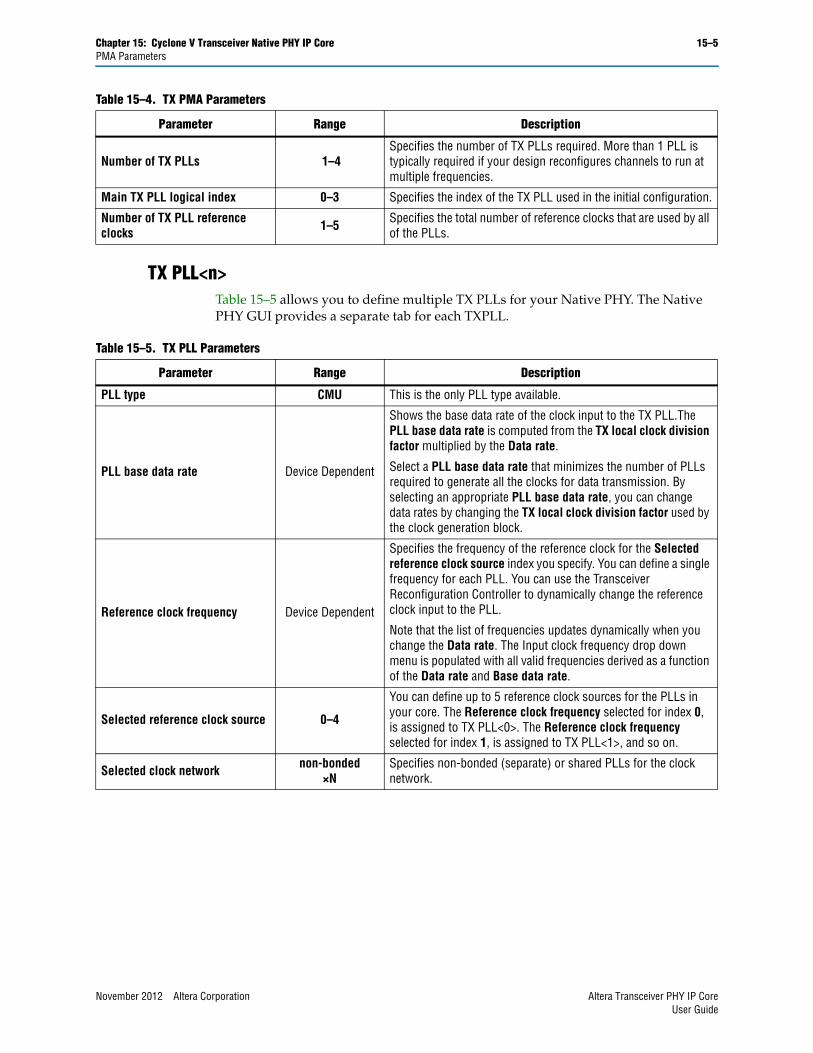
Chapter 15: Cyclone V Transceiver Native PHY IP Core 15–5PMA Parameters
TX PLL<n>Table 15–5 allows you to define multiple TX PLLs for your Native PHY. The Native PHY GUI provides a separate tab for each TXPLL.
Number of TX PLLs 1–4Specifies the number of TX PLLs required. More than 1 PLL is typically required if your design reconfigures channels to run at multiple frequencies.
Main TX PLL logical index 0–3 Specifies the index of the TX PLL used in the initial configuration.
Number of TX PLL reference clocks 1–5 Specifies the total number of reference clocks that are used by all
of the PLLs.
Table 15–4. TX PMA Parameters
Parameter Range Description
Table 15–5. TX PLL Parameters
Parameter Range Description
PLL type CMU This is the only PLL type available.
PLL base data rate Device Dependent
Shows the base data rate of the clock input to the TX PLL.The PLL base data rate is computed from the TX local clock division factor multiplied by the Data rate.
Select a PLL base data rate that minimizes the number of PLLs required to generate all the clocks for data transmission. By selecting an appropriate PLL base data rate, you can change data rates by changing the TX local clock division factor used by the clock generation block.
Reference clock frequency Device Dependent
Specifies the frequency of the reference clock for the Selected reference clock source index you specify. You can define a single frequency for each PLL. You can use the Transceiver Reconfiguration Controller to dynamically change the reference clock input to the PLL.
Note that the list of frequencies updates dynamically when you change the Data rate. The Input clock frequency drop down menu is populated with all valid frequencies derived as a function of the Data rate and Base data rate.
Selected reference clock source 0–4
You can define up to 5 reference clock sources for the PLLs in your core. The Reference clock frequency selected for index 0, is assigned to TX PLL<0>. The Reference clock frequency selected for index 1, is assigned to TX PLL<1>, and so on.
Selected clock network non-bonded×N
Specifies non-bonded (separate) or shared PLLs for the clock network.
November 2012 Altera Corporation Altera Transceiver PHY IP CoreUser Guide
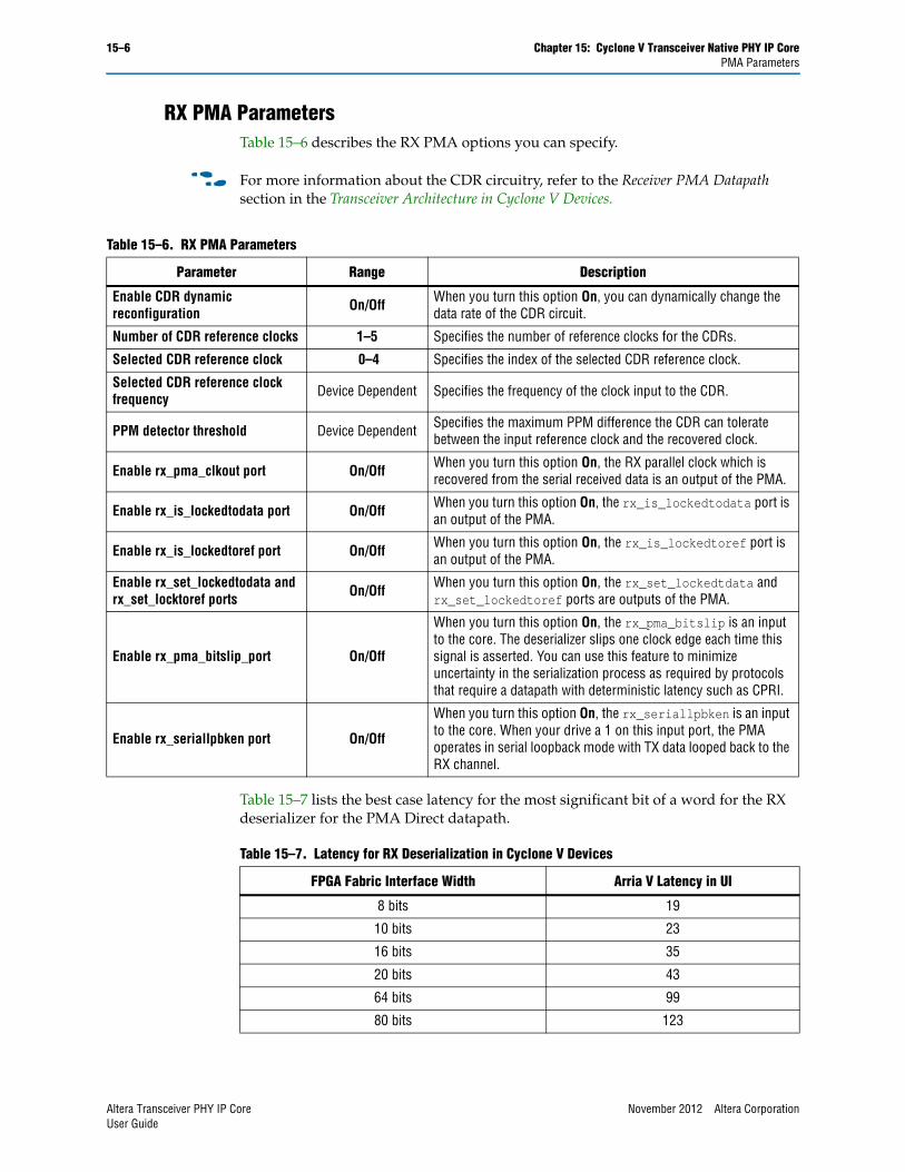
15–6 Chapter 15: Cyclone V Transceiver Native PHY IP CorePMA Parameters
RX PMA Parameters Table 15–6 describes the RX PMA options you can specify.
f For more information about the CDR circuitry, refer to the Receiver PMA Datapath section in the Transceiver Architecture in Cyclone V Devices.
Table 15–7 lists the best case latency for the most significant bit of a word for the RX deserializer for the PMA Direct datapath.
Table 15–6. RX PMA Parameters
Parameter Range Description
Enable CDR dynamic reconfiguration On/Off When you turn this option On, you can dynamically change the
data rate of the CDR circuit.
Number of CDR reference clocks 1–5 Specifies the number of reference clocks for the CDRs.
Selected CDR reference clock 0–4 Specifies the index of the selected CDR reference clock.
Selected CDR reference clock frequency Device Dependent Specifies the frequency of the clock input to the CDR.
PPM detector threshold Device Dependent Specifies the maximum PPM difference the CDR can tolerate between the input reference clock and the recovered clock.
Enable rx_pma_clkout port On/Off When you turn this option On, the RX parallel clock which is recovered from the serial received data is an output of the PMA.
Enable rx_is_lockedtodata port On/Off When you turn this option On, the rx_is_lockedtodata port is an output of the PMA.
Enable rx_is_lockedtoref port On/Off When you turn this option On, the rx_is_lockedtoref port is an output of the PMA.
Enable rx_set_lockedtodata and rx_set_locktoref ports On/Off When you turn this option On, the rx_set_lockedtdata and
rx_set_lockedtoref ports are outputs of the PMA.
Enable rx_pma_bitslip_port On/Off
When you turn this option On, the rx_pma_bitslip is an input to the core. The deserializer slips one clock edge each time this signal is asserted. You can use this feature to minimize uncertainty in the serialization process as required by protocols that require a datapath with deterministic latency such as CPRI.
Enable rx_seriallpbken port On/Off
When you turn this option On, the rx_seriallpbken is an input to the core. When your drive a 1 on this input port, the PMA operates in serial loopback mode with TX data looped back to the RX channel.
Table 15–7. Latency for RX Deserialization in Cyclone V Devices
FPGA Fabric Interface Width Arria V Latency in UI
8 bits 19
10 bits 23
16 bits 35
20 bits 43
64 bits 99
80 bits 123
Altera Transceiver PHY IP Core November 2012 Altera CorporationUser Guide

Chapter 15: Cyclone V Transceiver Native PHY IP Core 15–7PMA Parameters
Table 15–8 lists the best- case latency for the LSB of the TX serializer for all supported interface widths for the PMA Direct datapath.
Table 15–9 shows the bits used for all FPGA fabric to PMA interface widths. Regardless of the FPGA Fabric Interface Width selected, all 80 bits are exposed for the TX and RX parallel data ports. However, depending upon the interface width selected not all bits on the bus will be active. Table 15–9 shows which bits are active for each FPGA Fabric Interface Width selection. For example, if your interface is 16 bits, the active bits on the bus are [17:0] and [7:0] of the 80 bit bus. The non-active bits are tied to ground.
Table 15–8. Latency for TX Serialization in Cyclone V Devices
FPGA Fabric Interface Width Arria V Latency in UI
8 bits 43
10 bits 53
16 bits 67
20 bits 83
64 bits 131
80 bits 163
Table 15–9. Active Bits for Each Fabric Interface Width
FPGA Fabric Interface Width Bus Bits Used
8 bits [7:0]
10 bits [9:0]
16 bits {[17:10], [7:0]}
20 bits [19:0]
80 bits [79:0]
November 2012 Altera Corporation Altera Transceiver PHY IP CoreUser Guide
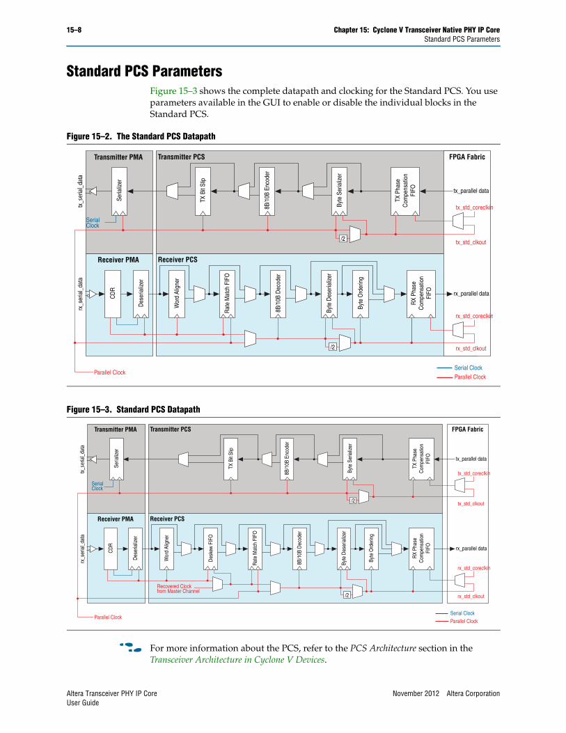
15–8 Chapter 15: Cyclone V Transceiver Native PHY IP CoreStandard PCS Parameters
Standard PCS ParametersFigure 15–3 shows the complete datapath and clocking for the Standard PCS. You use parameters available in the GUI to enable or disable the individual blocks in the Standard PCS.
f For more information about the PCS, refer to the PCS Architecture section in the Transceiver Architecture in Cyclone V Devices.
Figure 15–2. The Standard PCS Datapath
Transmitter PCSTransmitter PMA
Receiver PMA Receiver PCS
FPGA Fabric
Byte
Ord
erin
g
RX
Phas
eC
ompe
nsat
ion
FIFO
Byte
Des
eria
lizer
8B/1
0B D
ecod
er
Rat
e M
atch
FIF
O
Wor
d Al
igne
r
Des
eria
lizer
CD
R
TX P
hase
Com
pens
atio
nFI
FO
Byte
Ser
ializ
er
8B/1
0B E
ncod
er
TX B
it Sl
ip
Seria
lizer
rx_s
eria
l_da
tatx_
seria
l_data
tx_parallel data
rx_parallel data
/2
/2
tx_std_coreclkin
rx_std_coreclkin
Parallel Clock
SerialClock
Serial ClockParallel Clock
tx_std_clkout
rx_std_clkout
Figure 15–3. Standard PCS Datapath
Transmitter PCSTransmitter PMA
Receiver PMA Receiver PCS
FPGA Fabric
Byte
Ord
erin
g
RX
Phas
eC
ompe
nsat
ion
FIFO
Byte
Des
eria
lizer
8B/1
0B D
ecod
er
Rat
e M
atch
FIF
O
Des
kew
FIF
O
Wor
d Al
igne
r
Des
eria
lizer
CD
R
TX P
hase
Com
pens
atio
nFI
FO
Byte
Ser
ializ
er
8B/1
0B E
ncod
er
TX B
it Sl
ip
Seria
lizer
rx_s
eria
l_da
tatx_
seria
l_data
tx_parallel data
rx_parallel data
/2
/2
tx_std_coreclkin
rx_std_coreclkin
Recovered Clockfrom Master Channel
Parallel Clock
SerialClock
Serial ClockParallel Clock
tx_std_clkout
rx_std_clkout
Altera Transceiver PHY IP Core November 2012 Altera CorporationUser Guide
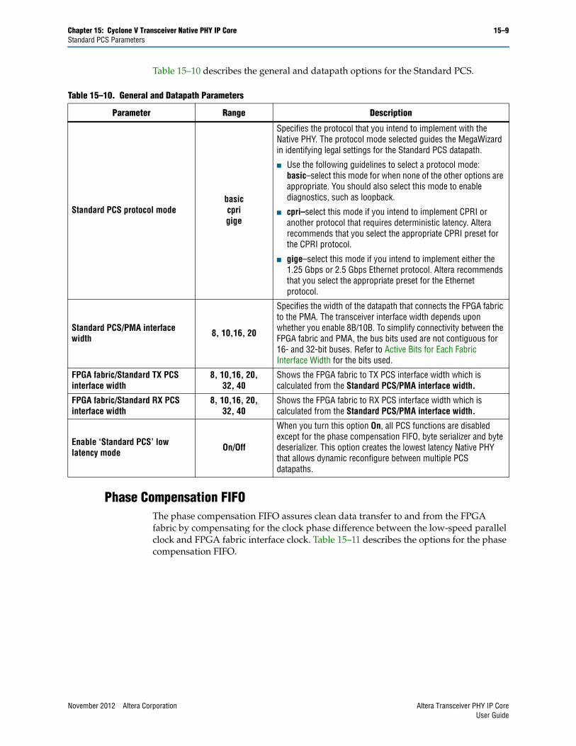
Chapter 15: Cyclone V Transceiver Native PHY IP Core 15–9Standard PCS Parameters
Table 15–10 describes the general and datapath options for the Standard PCS.
Phase Compensation FIFOThe phase compensation FIFO assures clean data transfer to and from the FPGA fabric by compensating for the clock phase difference between the low-speed parallel clock and FPGA fabric interface clock. Table 15–11 describes the options for the phase compensation FIFO.
Table 15–10. General and Datapath Parameters
Parameter Range Description
Standard PCS protocol modebasiccprigige
Specifies the protocol that you intend to implement with the Native PHY. The protocol mode selected guides the MegaWizard in identifying legal settings for the Standard PCS datapath.
■ Use the following guidelines to select a protocol mode: basic–select this mode for when none of the other options are appropriate. You should also select this mode to enable diagnostics, such as loopback.
■ cpri–select this mode if you intend to implement CPRI or another protocol that requires deterministic latency. Altera recommends that you select the appropriate CPRI preset for the CPRI protocol.
■ gige–select this mode if you intend to implement either the 1.25 Gbps or 2.5 Gbps Ethernet protocol. Altera recommends that you select the appropriate preset for the Ethernet protocol.
Standard PCS/PMA interface width 8, 10,16, 20
Specifies the width of the datapath that connects the FPGA fabric to the PMA. The transceiver interface width depends upon whether you enable 8B/10B. To simplify connectivity between the FPGA fabric and PMA, the bus bits used are not contiguous for 16- and 32-bit buses. Refer to Active Bits for Each Fabric Interface Width for the bits used.
FPGA fabric/Standard TX PCS interface width
8, 10,16, 20, 32, 40
Shows the FPGA fabric to TX PCS interface width which is calculated from the Standard PCS/PMA interface width.
FPGA fabric/Standard RX PCS interface width
8, 10,16, 20, 32, 40
Shows the FPGA fabric to RX PCS interface width which is calculated from the Standard PCS/PMA interface width.
Enable ‘Standard PCS’ low latency mode On/Off
When you turn this option On, all PCS functions are disabled except for the phase compensation FIFO, byte serializer and byte deserializer. This option creates the lowest latency Native PHY that allows dynamic reconfigure between multiple PCS datapaths.
November 2012 Altera Corporation Altera Transceiver PHY IP CoreUser Guide
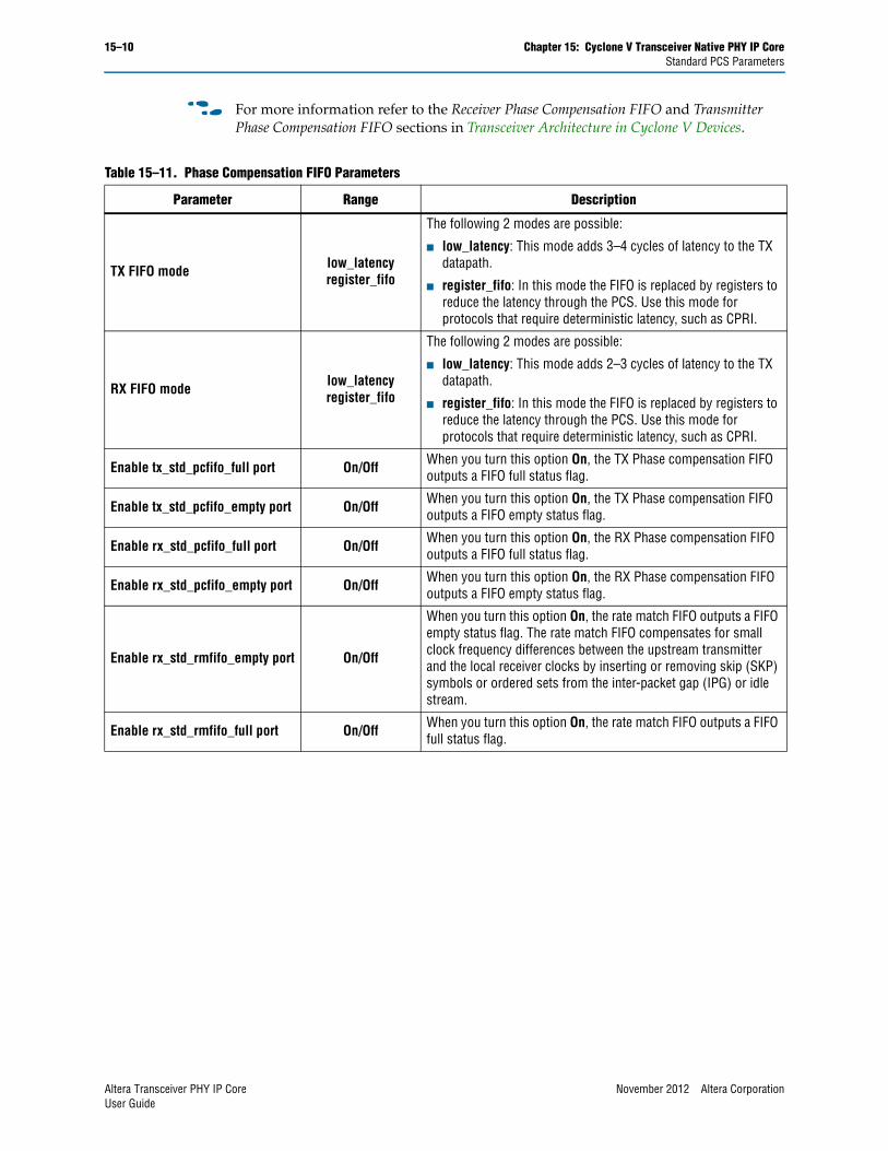
15–10 Chapter 15: Cyclone V Transceiver Native PHY IP CoreStandard PCS Parameters
f For more information refer to the Receiver Phase Compensation FIFO and Transmitter Phase Compensation FIFO sections in Transceiver Architecture in Cyclone V Devices.
Table 15–11. Phase Compensation FIFO Parameters
Parameter Range Description
TX FIFO mode low_latencyregister_fifo
The following 2 modes are possible:
■ low_latency: This mode adds 3–4 cycles of latency to the TX datapath.
■ register_fifo: In this mode the FIFO is replaced by registers to reduce the latency through the PCS. Use this mode for protocols that require deterministic latency, such as CPRI.
RX FIFO mode low_latencyregister_fifo
The following 2 modes are possible:
■ low_latency: This mode adds 2–3 cycles of latency to the TX datapath.
■ register_fifo: In this mode the FIFO is replaced by registers to reduce the latency through the PCS. Use this mode for protocols that require deterministic latency, such as CPRI.
Enable tx_std_pcfifo_full port On/Off When you turn this option On, the TX Phase compensation FIFO outputs a FIFO full status flag.
Enable tx_std_pcfifo_empty port On/Off When you turn this option On, the TX Phase compensation FIFO outputs a FIFO empty status flag.
Enable rx_std_pcfifo_full port On/Off When you turn this option On, the RX Phase compensation FIFO outputs a FIFO full status flag.
Enable rx_std_pcfifo_empty port On/Off When you turn this option On, the RX Phase compensation FIFO outputs a FIFO empty status flag.
Enable rx_std_rmfifo_empty port On/Off
When you turn this option On, the rate match FIFO outputs a FIFO empty status flag. The rate match FIFO compensates for small clock frequency differences between the upstream transmitter and the local receiver clocks by inserting or removing skip (SKP) symbols or ordered sets from the inter-packet gap (IPG) or idle stream.
Enable rx_std_rmfifo_full port On/Off When you turn this option On, the rate match FIFO outputs a FIFO full status flag.
Altera Transceiver PHY IP Core November 2012 Altera CorporationUser Guide
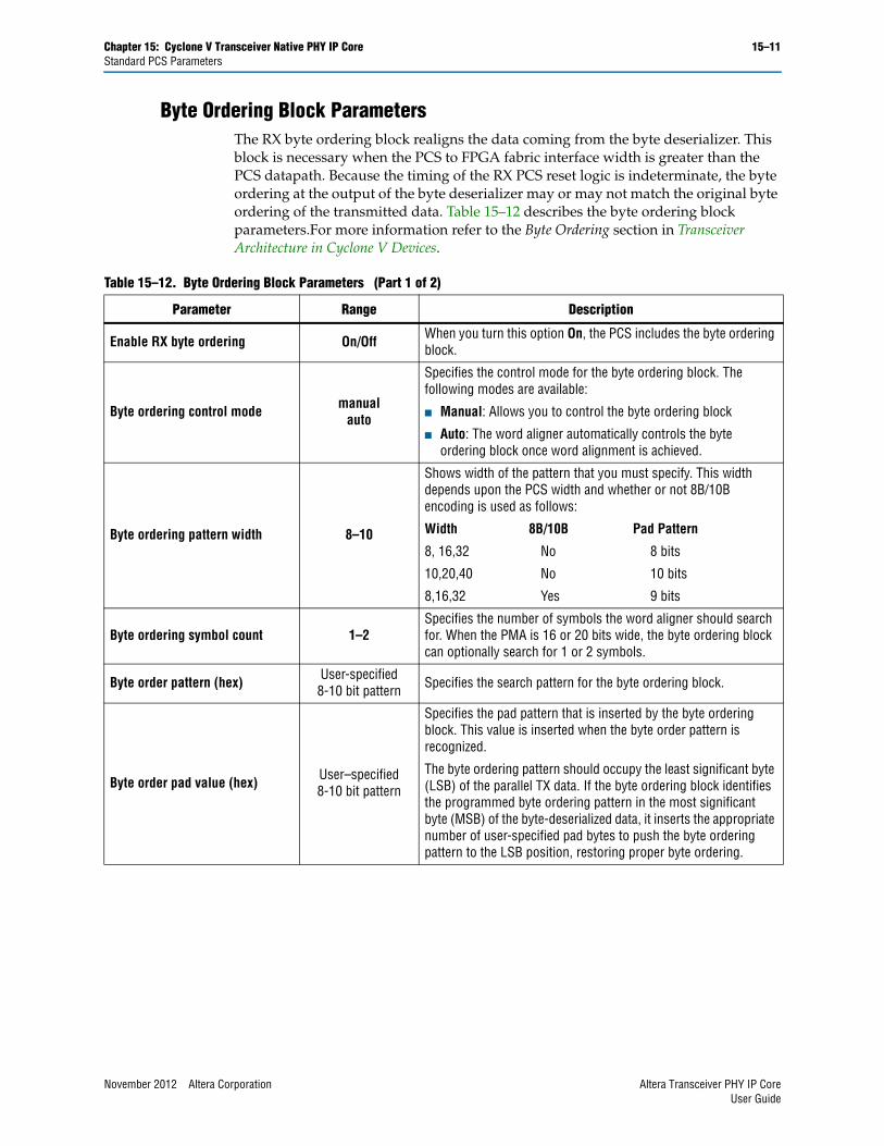
Chapter 15: Cyclone V Transceiver Native PHY IP Core 15–11Standard PCS Parameters
Byte Ordering Block ParametersThe RX byte ordering block realigns the data coming from the byte deserializer. This block is necessary when the PCS to FPGA fabric interface width is greater than the PCS datapath. Because the timing of the RX PCS reset logic is indeterminate, the byte ordering at the output of the byte deserializer may or may not match the original byte ordering of the transmitted data. Table 15–12 describes the byte ordering block parameters.For more information refer to the Byte Ordering section in Transceiver Architecture in Cyclone V Devices.
Table 15–12. Byte Ordering Block Parameters (Part 1 of 2)
Parameter Range Description
Enable RX byte ordering On/Off When you turn this option On, the PCS includes the byte ordering block.
Byte ordering control mode manualauto
Specifies the control mode for the byte ordering block. The following modes are available:
■ Manual: Allows you to control the byte ordering block
■ Auto: The word aligner automatically controls the byte ordering block once word alignment is achieved.
Byte ordering pattern width 8–10
Shows width of the pattern that you must specify. This width depends upon the PCS width and whether or not 8B/10B encoding is used as follows:
Width 8B/10B Pad Pattern
8, 16,32 No 8 bits
10,20,40 No 10 bits
8,16,32 Yes 9 bits
Byte ordering symbol count 1–2Specifies the number of symbols the word aligner should search for. When the PMA is 16 or 20 bits wide, the byte ordering block can optionally search for 1 or 2 symbols.
Byte order pattern (hex) User-specified 8-10 bit pattern Specifies the search pattern for the byte ordering block.
Byte order pad value (hex) User–specified 8-10 bit pattern
Specifies the pad pattern that is inserted by the byte ordering block. This value is inserted when the byte order pattern is recognized.
The byte ordering pattern should occupy the least significant byte (LSB) of the parallel TX data. If the byte ordering block identifies the programmed byte ordering pattern in the most significant byte (MSB) of the byte-deserialized data, it inserts the appropriate number of user-specified pad bytes to push the byte ordering pattern to the LSB position, restoring proper byte ordering.
November 2012 Altera Corporation Altera Transceiver PHY IP CoreUser Guide
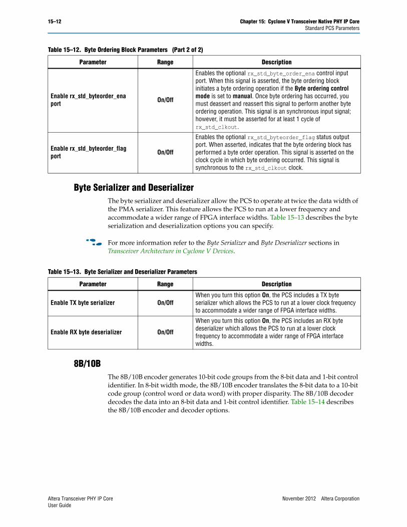
15–12 Chapter 15: Cyclone V Transceiver Native PHY IP CoreStandard PCS Parameters
Byte Serializer and DeserializerThe byte serializer and deserializer allow the PCS to operate at twice the data width of the PMA serializer. This feature allows the PCS to run at a lower frequency and accommodate a wider range of FPGA interface widths. Table 15–13 describes the byte serialization and deserialization options you can specify.
f For more information refer to the Byte Serializer and Byte Deserializer sections in Transceiver Architecture in Cyclone V Devices.
8B/10BThe 8B/10B encoder generates 10-bit code groups from the 8-bit data and 1-bit control identifier. In 8-bit width mode, the 8B/10B encoder translates the 8-bit data to a 10-bit code group (control word or data word) with proper disparity. The 8B/10B decoder decodes the data into an 8-bit data and 1-bit control identifier. Table 15–14 describes the 8B/10B encoder and decoder options.
Enable rx_std_byteorder_ena port On/Off
Enables the optional rx_std_byte_order_ena control input port. When this signal is asserted, the byte ordering block initiates a byte ordering operation if the Byte ordering control mode is set to manual. Once byte ordering has occurred, you must deassert and reassert this signal to perform another byte ordering operation. This signal is an synchronous input signal; however, it must be asserted for at least 1 cycle of rx_std_clkout.
Enable rx_std_byteorder_flag port On/Off
Enables the optional rx_std_byteorder_flag status output port. When asserted, indicates that the byte ordering block has performed a byte order operation. This signal is asserted on the clock cycle in which byte ordering occurred. This signal is synchronous to the rx_std_clkout clock.
Table 15–12. Byte Ordering Block Parameters (Part 2 of 2)
Parameter Range Description
Table 15–13. Byte Serializer and Deserializer Parameters
Parameter Range Description
Enable TX byte serializer On/OffWhen you turn this option On, the PCS includes a TX byte serializer which allows the PCS to run at a lower clock frequency to accommodate a wider range of FPGA interface widths.
Enable RX byte deserializer On/Off
When you turn this option On, the PCS includes an RX byte deserializer which allows the PCS to run at a lower clock frequency to accommodate a wider range of FPGA interface widths.
Altera Transceiver PHY IP Core November 2012 Altera CorporationUser Guide
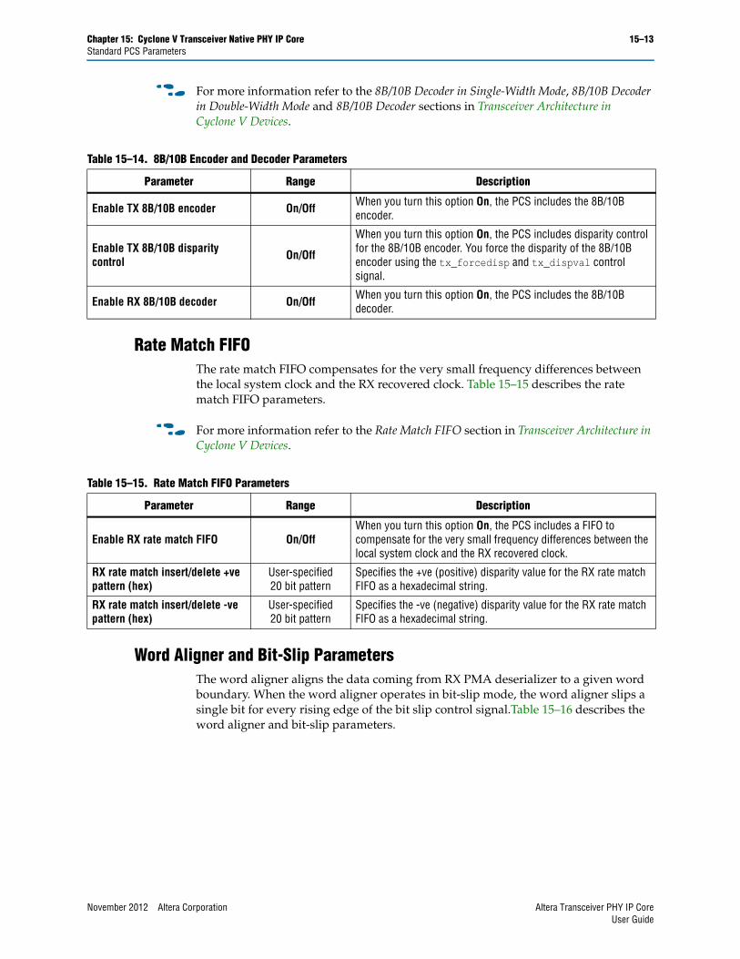
Chapter 15: Cyclone V Transceiver Native PHY IP Core 15–13Standard PCS Parameters
f For more information refer to the 8B/10B Decoder in Single-Width Mode, 8B/10B Decoder in Double-Width Mode and 8B/10B Decoder sections in Transceiver Architecture in Cyclone V Devices.
Rate Match FIFOThe rate match FIFO compensates for the very small frequency differences between the local system clock and the RX recovered clock. Table 15–15 describes the rate match FIFO parameters.
f For more information refer to the Rate Match FIFO section in Transceiver Architecture in Cyclone V Devices.
Word Aligner and Bit-Slip ParametersThe word aligner aligns the data coming from RX PMA deserializer to a given word boundary. When the word aligner operates in bit-slip mode, the word aligner slips a single bit for every rising edge of the bit slip control signal.Table 15–16 describes the word aligner and bit-slip parameters.
Table 15–14. 8B/10B Encoder and Decoder Parameters
Parameter Range Description
Enable TX 8B/10B encoder On/Off When you turn this option On, the PCS includes the 8B/10B encoder.
Enable TX 8B/10B disparity control On/Off
When you turn this option On, the PCS includes disparity control for the 8B/10B encoder. You force the disparity of the 8B/10B encoder using the tx_forcedisp and tx_dispval control signal.
Enable RX 8B/10B decoder On/Off When you turn this option On, the PCS includes the 8B/10B decoder.
Table 15–15. Rate Match FIFO Parameters
Parameter Range Description
Enable RX rate match FIFO On/OffWhen you turn this option On, the PCS includes a FIFO to compensate for the very small frequency differences between the local system clock and the RX recovered clock.
RX rate match insert/delete +ve pattern (hex)
User-specified 20 bit pattern
Specifies the +ve (positive) disparity value for the RX rate match FIFO as a hexadecimal string.
RX rate match insert/delete -ve pattern (hex)
User-specified 20 bit pattern
Specifies the -ve (negative) disparity value for the RX rate match FIFO as a hexadecimal string.
November 2012 Altera Corporation Altera Transceiver PHY IP CoreUser Guide
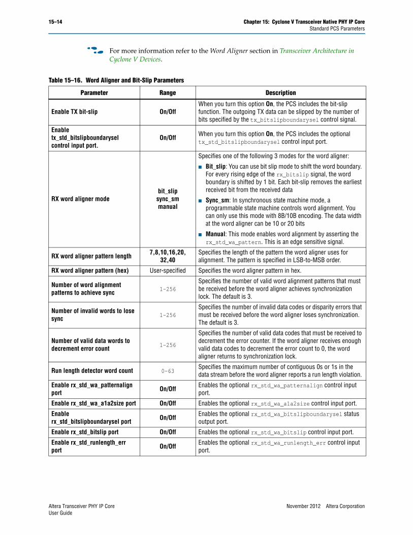
15–14 Chapter 15: Cyclone V Transceiver Native PHY IP CoreStandard PCS Parameters
f For more information refer to the Word Aligner section in Transceiver Architecture in Cyclone V Devices.
Table 15–16. Word Aligner and Bit-Slip Parameters
Parameter Range Description
Enable TX bit-slip On/OffWhen you turn this option On, the PCS includes the bit-slip function. The outgoing TX data can be slipped by the number of bits specified by the tx_bitslipboundarysel control signal.
Enable tx_std_bitslipboundarysel control input port.
On/Off When you turn this option On, the PCS includes the optional tx_std_bitslipboundarysel control input port.
RX word aligner modebit_slipsync_smmanual
Specifies one of the following 3 modes for the word aligner:
■ Bit_slip: You can use bit slip mode to shift the word boundary. For every rising edge of the rx_bitslip signal, the word boundary is shifted by 1 bit. Each bit-slip removes the earliest received bit from the received data
■ Sync_sm: In synchronous state machine mode, a programmable state machine controls word alignment. You can only use this mode with 8B/10B encoding. The data width at the word aligner can be 10 or 20 bits
■ Manual: This mode enables word alignment by asserting the rx_std_wa_pattern. This is an edge sensitive signal.
RX word aligner pattern length 7,8,10,16,20,32,40
Specifies the length of the pattern the word aligner uses for alignment. The pattern is specified in LSB-to-MSB order.
RX word aligner pattern (hex) User-specified Specifies the word aligner pattern in hex.
Number of word alignment patterns to achieve sync 1–256
Specifies the number of valid word alignment patterns that must be received before the word aligner achieves synchronization lock. The default is 3.
Number of invalid words to lose sync 1–256
Specifies the number of invalid data codes or disparity errors that must be received before the word aligner loses synchronization. The default is 3.
Number of valid data words to decrement error count 1–256
Specifies the number of valid data codes that must be received to decrement the error counter. If the word aligner receives enough valid data codes to decrement the error count to 0, the word aligner returns to synchronization lock.
Run length detector word count 0–63Specifies the maximum number of contiguous 0s or 1s in the data stream before the word aligner reports a run length violation.
Enable rx_std_wa_patternalign port On/Off Enables the optional rx_std_wa_patternalign control input
port.
Enable rx_std_wa_a1a2size port On/Off Enables the optional rx_std_wa_a1a2size control input port.
Enable rx_std_bitslipboundarysel port On/Off Enables the optional rx_std_wa_bitslipboundarysel status
output port.
Enable rx_std_bitslip port On/Off Enables the optional rx_std_wa_bitslip control input port.
Enable rx_std_runlength_err port On/Off Enables the optional rx_std_wa_runlength_err control input
port.
Altera Transceiver PHY IP Core November 2012 Altera CorporationUser Guide
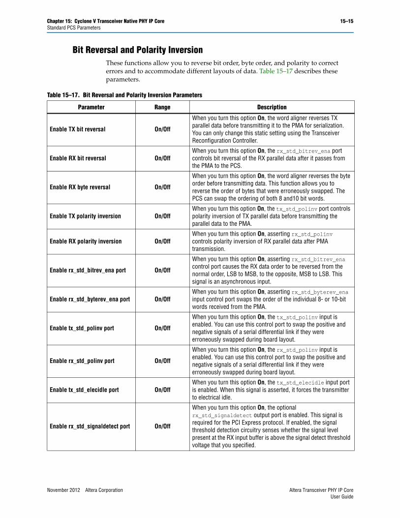
Chapter 15: Cyclone V Transceiver Native PHY IP Core 15–15Standard PCS Parameters
Bit Reversal and Polarity InversionThese functions allow you to reverse bit order, byte order, and polarity to correct errors and to accommodate different layouts of data. Table 15–17 describes these parameters.
Table 15–17. Bit Reversal and Polarity Inversion Parameters
Parameter Range Description
Enable TX bit reversal On/Off
When you turn this option On, the word aligner reverses TX parallel data before transmitting it to the PMA for serialization. You can only change this static setting using the Transceiver Reconfiguration Controller.
Enable RX bit reversal On/OffWhen you turn this option On, the rx_std_bitrev_ena port controls bit reversal of the RX parallel data after it passes from the PMA to the PCS.
Enable RX byte reversal On/Off
When you turn this option On, the word aligner reverses the byte order before transmitting data. This function allows you to reverse the order of bytes that were erroneously swapped. The PCS can swap the ordering of both 8 and10 bit words.
Enable TX polarity inversion On/OffWhen you turn this option On, the tx_std_polinv port controls polarity inversion of TX parallel data before transmitting the parallel data to the PMA.
Enable RX polarity inversion On/OffWhen you turn this option On, asserting rx_std_polinv controls polarity inversion of RX parallel data after PMA transmission.
Enable rx_std_bitrev_ena port On/Off
When you turn this option On, asserting rx_std_bitrev_ena control port causes the RX data order to be reversed from the normal order, LSB to MSB, to the opposite, MSB to LSB. This signal is an asynchronous input.
Enable rx_std_byterev_ena port On/OffWhen you turn this option On, asserting rx_std_byterev_ena input control port swaps the order of the individual 8- or 10-bit words received from the PMA.
Enable tx_std_polinv port On/Off
When you turn this option On, the tx_std_polinv input is enabled. You can use this control port to swap the positive and negative signals of a serial differential link if they were erroneously swapped during board layout.
Enable rx_std_polinv port On/Off
When you turn this option On, the rx_std_polinv input is enabled. You can use this control port to swap the positive and negative signals of a serial differential link if they were erroneously swapped during board layout.
Enable tx_std_elecidle port On/OffWhen you turn this option On, the tx_std_elecidle input port is enabled. When this signal is asserted, it forces the transmitter to electrical idle.
Enable rx_std_signaldetect port On/Off
When you turn this option On, the optional rx_std_signaldetect output port is enabled. This signal is required for the PCI Express protocol. If enabled, the signal threshold detection circuitry senses whether the signal level present at the RX input buffer is above the signal detect threshold voltage that you specified.
November 2012 Altera Corporation Altera Transceiver PHY IP CoreUser Guide
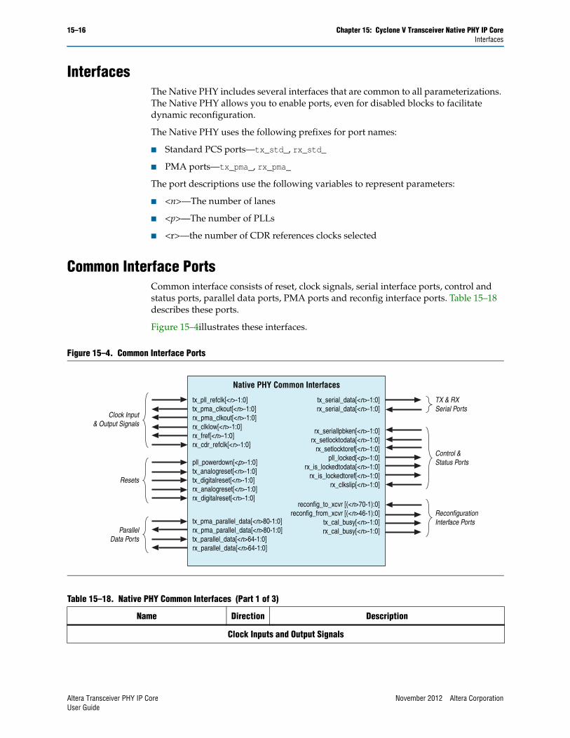
15–16 Chapter 15: Cyclone V Transceiver Native PHY IP CoreInterfaces
InterfacesThe Native PHY includes several interfaces that are common to all parameterizations. The Native PHY allows you to enable ports, even for disabled blocks to facilitate dynamic reconfiguration.
The Native PHY uses the following prefixes for port names:
■ Standard PCS ports—tx_std_, rx_std_
■ PMA ports—tx_pma_, rx_pma_
The port descriptions use the following variables to represent parameters:
■ <n>—The number of lanes
■ <p>—The number of PLLs
■ <r>—the number of CDR references clocks selected
Common Interface PortsCommon interface consists of reset, clock signals, serial interface ports, control and status ports, parallel data ports, PMA ports and reconfig interface ports. Table 15–18 describes these ports.
Figure 15–4illustrates these interfaces.
Figure 15–4. Common Interface Ports
tx_pll_refclk[<r>-1:0]tx_pma_clkout[<n>-1:0]rx_pma_clkout[<n>-1:0]rx_clklow[<n>-1:0]rx_fref[<n>-1:0]rx_cdr_refclk[<r>-1:0]
Clock Input& Output Signals
rx_seriallpbken[<n>-1:0]rx_setlocktodata[<n>-1:0]
rx_setlocktoref[<n>-1:0]pll_locked[<p>-1:0]
rx_is_lockedtodata[<n>-1:0]rx_is_lockedtoref[<n>-1:0]
rx_clkslip[<n>-1:0]
Control &Status Portspll_powerdown[<p>-1:0]
tx_analogreset[<n>-1:0]tx_digitalreset[<n>-1:0]rx_analogreset[<n>-1:0]rx_digitalreset[<n>-1:0]
Resets
tx_pma_parallel_data[<n>80-1:0]rx_pma_parallel_data[<n>80-1:0]tx_parallel_data[<n>64-1:0]rx_parallel_data[<n>64-1:0]
ParallelData Ports
tx_serial_data[<n>-1:0]rx_serial_data[<n>-1:0]
TX & RXSerial Ports
reconfig_to_xcvr [(<n>70-1):0]reconfig_from_xcvr [(<n>46-1):0]
tx_cal_busy[<n>-1:0]rx_cal_busy[<n>-1:0]
ReconfigurationInterface Ports
Native PHY Common Interfaces
Table 15–18. Native PHY Common Interfaces (Part 1 of 3)
Name Direction Description
Clock Inputs and Output Signals
Altera Transceiver PHY IP Core November 2012 Altera CorporationUser Guide
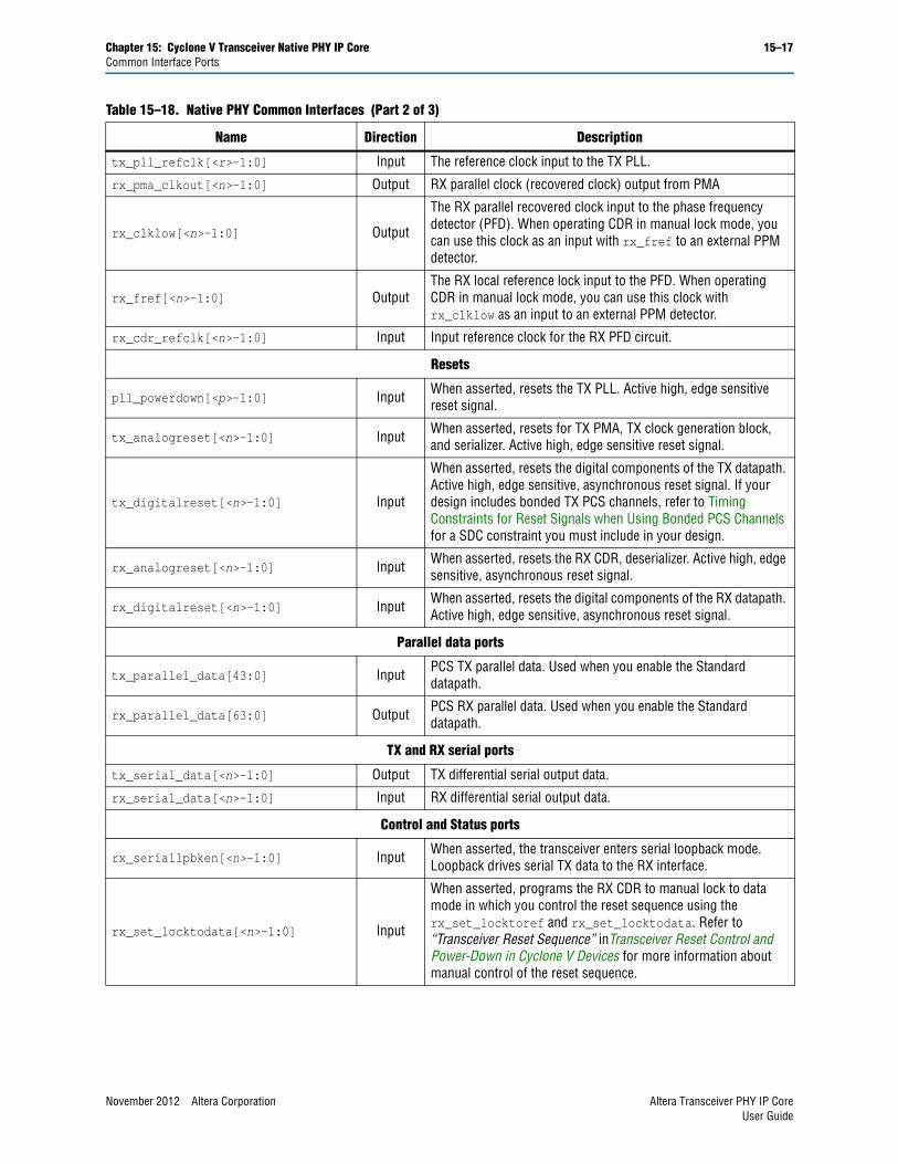
Chapter 15: Cyclone V Transceiver Native PHY IP Core 15–17Common Interface Ports
tx_pll_refclk[<r>-1:0] Input The reference clock input to the TX PLL.
rx_pma_clkout[<n>-1:0] Output RX parallel clock (recovered clock) output from PMA
rx_clklow[<n>-1:0] Output
The RX parallel recovered clock input to the phase frequency detector (PFD). When operating CDR in manual lock mode, you can use this clock as an input with rx_fref to an external PPM detector.
rx_fref[<n>-1:0] OutputThe RX local reference lock input to the PFD. When operating CDR in manual lock mode, you can use this clock with rx_clklow as an input to an external PPM detector.
rx_cdr_refclk[<n>-1:0] Input Input reference clock for the RX PFD circuit.
Resets
pll_powerdown[<p>-1:0] Input When asserted, resets the TX PLL. Active high, edge sensitive reset signal.
tx_analogreset[<n>-1:0] Input When asserted, resets for TX PMA, TX clock generation block, and serializer. Active high, edge sensitive reset signal.
tx_digitalreset[<n>-1:0] Input
When asserted, resets the digital components of the TX datapath. Active high, edge sensitive, asynchronous reset signal. If your design includes bonded TX PCS channels, refer to Timing Constraints for Reset Signals when Using Bonded PCS Channels for a SDC constraint you must include in your design.
rx_analogreset[<n>-1:0] Input When asserted, resets the RX CDR, deserializer. Active high, edge sensitive, asynchronous reset signal.
rx_digitalreset[<n>-1:0] Input When asserted, resets the digital components of the RX datapath. Active high, edge sensitive, asynchronous reset signal.
Parallel data ports
tx_parallel_data[43:0] Input PCS TX parallel data. Used when you enable the Standard datapath.
rx_parallel_data[63:0] Output PCS RX parallel data. Used when you enable the Standard datapath.
TX and RX serial ports
tx_serial_data[<n>-1:0] Output TX differential serial output data.
rx_serial_data[<n>-1:0] Input RX differential serial output data.
Control and Status ports
rx_seriallpbken[<n>-1:0] Input When asserted, the transceiver enters serial loopback mode. Loopback drives serial TX data to the RX interface.
rx_set_locktodata[<n>-1:0] Input
When asserted, programs the RX CDR to manual lock to data mode in which you control the reset sequence using the rx_set_locktoref and rx_set_locktodata. Refer to “Transceiver Reset Sequence” inTransceiver Reset Control and Power-Down in Cyclone V Devices for more information about manual control of the reset sequence.
Table 15–18. Native PHY Common Interfaces (Part 2 of 3)
Name Direction Description
November 2012 Altera Corporation Altera Transceiver PHY IP CoreUser Guide
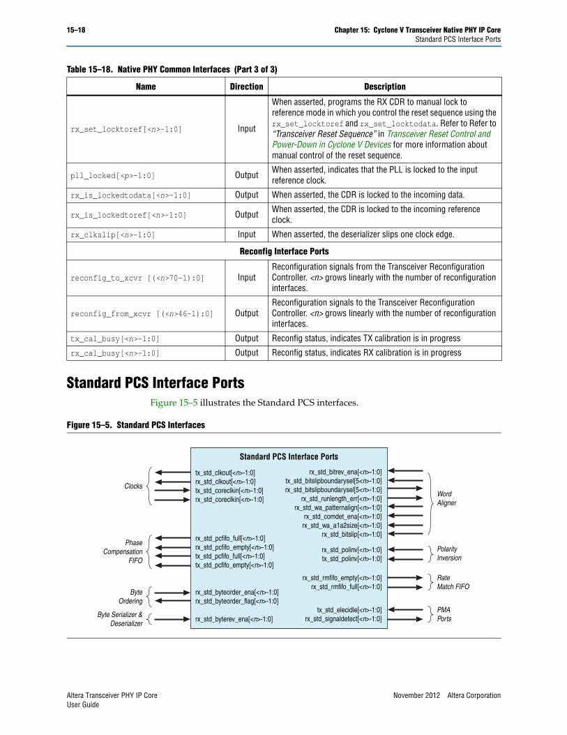
15–18 Chapter 15: Cyclone V Transceiver Native PHY IP CoreStandard PCS Interface Ports
Standard PCS Interface PortsFigure 15–5 illustrates the Standard PCS interfaces.
rx_set_locktoref[<n>-1:0] Input
When asserted, programs the RX CDR to manual lock to reference mode in which you control the reset sequence using the rx_set_locktoref and rx_set_locktodata. Refer to Refer to “Transceiver Reset Sequence” in Transceiver Reset Control and Power-Down in Cyclone V Devices for more information about manual control of the reset sequence.
pll_locked[<p>-1:0] Output When asserted, indicates that the PLL is locked to the input reference clock.
rx_is_lockedtodata[<n>-1:0] Output When asserted, the CDR is locked to the incoming data.
rx_is_lockedtoref[<n>-1:0] Output When asserted, the CDR is locked to the incoming reference clock.
rx_clkslip[<n>-1:0] Input When asserted, the deserializer slips one clock edge.
Reconfig Interface Ports
reconfig_to_xcvr [(<n>70-1):0] InputReconfiguration signals from the Transceiver Reconfiguration Controller. <n> grows linearly with the number of reconfiguration interfaces.
reconfig_from_xcvr [(<n>46-1):0] OutputReconfiguration signals to the Transceiver Reconfiguration Controller. <n> grows linearly with the number of reconfiguration interfaces.
tx_cal_busy[<n>-1:0] Output Reconfig status, indicates TX calibration is in progress
rx_cal_busy[<n>-1:0] Output Reconfig status, indicates RX calibration is in progress
Table 15–18. Native PHY Common Interfaces (Part 3 of 3)
Name Direction Description
Figure 15–5. Standard PCS Interfaces
tx_std_clkout[<n>-1:0] rx_std_clkout[<n>-1:0]tx_std_coreclkin[<n>-1:0]rx_std_coreclkin[<n>-1:0]
ClocksWordAligner
rx_std_pcfifo_full[<n>-1:0] rx_std_pcfifo_empty[<n>-1:0] tx_std_pcfifo_full[<n>-1:0] tx_std_pcfifo_empty[<n>-1:0]
PhaseCompensation
FIFO
rx_std_byteorder_ena[<n>-1:0] rx_std_byteorder_flag[<n>-1:0]
ByteOrdering
rx_std_rmfifo_empty[<n>-1:0]rx_std_rmfifo_full[<n>-1:0]
RateMatch FIFO
rx_std_polinv[<n>-1:0]tx_std_polinv[<n>-1:0]
PolarityInversion
PMAPorts
Standard PCS Interface Ports
rx_std_bitrev_ena[<n>-1:0]tx_std_bitslipboundarysel[5<n>-1:0]rx_std_bitslipboundarysel[5<n>-1:0]
rx_std_runlength_err[<n>-1:0]rx_std_wa_patternalign[<n>-1:0]
rx_std_comdet_ena[<n>-1:0]rx_std_wa_a1a2size[<n>-1:0]
rx_std_bitslip[<n>-1:0]
tx_std_elecidle[<n>-1:0]rx_std_signaldetect[<n>-1:0]rx_std_byterev_ena[<n>-1:0]
Byte Serializer &Deserializer
Altera Transceiver PHY IP Core November 2012 Altera CorporationUser Guide
Chapter 15: Cyclone V Transceiver Native PHY IP Core 15–19Standard PCS Interface Ports
Table 15–19 describes the ports available for the Standard PCS interface.
Table 15–19. Standard PCS Interface Ports (Part 1 of 3)
Name Dir
Synchronous to
tx_std_coreclkin/
rx_std_coreclkin
Description
Clocks
tx_std_clkout[<n>-1:0] Output — TX Parallel clock output as shown in The Standard PCS Datapath figure.
rx_std_clkout[<n>-1:0] Output —RX parallel clock output as shown in The Standard PCS Datapath figure. The CDR circuitry recovers RX parallel clock from the RX data stream.
tx_std_coreclkin[<n>-1:0] Input —TX parallel clock input from the FPGA fabric that drives the write side of the TX phase compensation FIFO as shown in The Standard PCS Datapath figure.
rx_std_coreclkin[<n>-1:0] Input — RX parallel clock that drives the read side of the RX phase compensation FIFO The Standard PCS Datapath figure.
Phase Compensation FIFO
rx_std_pcfifo_full[<n>-1:0]
Output Yes RX phase compensation FIFO full status flag.
rx_std_pcfifo_empty[<n>-1:0]
Output Yes RX phase compensation FIFO status empty flag.
tx_std_pcfifo_full[<n>-1:0]
Output Yes TX phase compensation FIFO status full flag.
tx_std_pcfifo_empty[<n>-1:0]
Output Yes TX phase compensation FIFO status empty flag.
Byte Ordering
rx_std_byteorder_ena[<n>-1:0]
Input No
Byte ordering enable. When this signal is asserted, the byte ordering block initiates a byte ordering operation if the Byte ordering control mode is set to manual. Once byte ordering has occurred, you must deassert and reassert this signal to perform another byte ordering operation. This signal is an synchronous input signal; however, it must be asserted for at least 1 cycle of rx_std_clkout.
rx_std_byteorder_flag[<n>-1:0]
Output Yes
Byte ordering status flag. When asserted, indicates that the byte ordering block has performed a byte order operation. This signal is asserted on the clock cycle in which byte ordering occurred. This signal is synchronous to the rx_std_clkout clock. You must a synchronizer this signal.
Byte Serializer and Deserializer
rx_std_byterev_ena[<n>-1:0]
Input NoThis control signal is available in when the PMA width is 16 or 20 bits. When asserted, enables byte reversal on the RX interface.
November 2012 Altera Corporation Altera Transceiver PHY IP CoreUser Guide
15–20 Chapter 15: Cyclone V Transceiver Native PHY IP CoreStandard PCS Interface Ports
8B/10B
rx_std_polinv[<n>-1:0] Input No
Polarity inversion for the 8B/10B decoder, When set, the RX channels invert the polarity of the received data. You can use this signal to correct the polarity of differential pairs if the transmission circuitry or board layout mistakenly swapped the positive and negative signals. The polarity inversion function operates on the word aligner input.
tx_std_polinv[<n>-1:0] Input No Polarity inversion, part of 8B10B encoder, When set, the TX interface inverts the polarity of the TX data.
Rate Match FIFO
rx_std_rmfifo_empty[<n>-1:0]
Output No Rate match FIFO empty flag. When asserted, the rate match FIFO is empty.
rx_std_rmfifo_full[<n>-1:0]
Output No Rate match FIFO full flag. When asserted the rate match FIFO is full. You must synchronize this signal.
Word Aligner
rx_std_bitrev_ena[<n>-1:0]
Input No
When asserted, enables bit reversal on the RX interface. Bit order may be reversed if external transmission circuitry transmits the most significant bit first. When enabled, the receive circuitry receives all words in the reverse order. The bit reversal circuitry operates on the output of the word aligner.
tx_std_bitslipboundarysel[5<n>-1:0]
Input No Bit-Slip boundary selection signal. Specifies the number of bits that the TX bit slipper must slip.
rx_std_bitslipboundarysel[5<n>-1:0]
Output NoThis signal operates when the word aligner is in bit-slip word alignment mode. It reports the number of bits that the RX block slipped to achieve deterministic latency.
rx_std_runlength_err[<n>-1:0]
Output NoWhen asserted, indicates a run length violation. Asserted if the number of consecutive 1s or 0s exceeds the number specified in the parameter editor GUI.
rx_st_wa_patternalign Input No
Active when you place the word aligner in manual mode. In manual mode, you align words by asserting rx_st_wa_patternalign. rx_st_wa_patternalign is edge sensitive.
For more information refer to the Word Aligner section in Transceiver Architecture in Cyclone V Devices.
rx_std_wa_a1a2size[<n>-1:0]
Input No
Used for the SONET protocol. Assert when the A1 and A2 framing bytes must be detected. A1 and A2 are SONET backplane bytes and are only used when the PMA data width is 8 bits.
Table 15–19. Standard PCS Interface Ports (Part 2 of 3)
Name Dir
Synchronous to
tx_std_coreclkin/
rx_std_coreclkin
Description
Altera Transceiver PHY IP Core November 2012 Altera CorporationUser Guide
Chapter 15: Cyclone V Transceiver Native PHY IP Core 15–21SDC Timing Constraints
SDC Timing Constraints The Quartus II 12.1 software reports timing violations for asynchronous inputs to the Standard PCS and 10G PCS. Because many violations are for asynchronous paths, they do not represent actual timing failures. You may choose one of the following three approaches to identify these false timing paths to the Quartus II or TimeQuest software.
rx_std_bitslip[<n>-1:0] Input No
Used when word aligner mode is bit-slip mode. For every rising edge of the rx_std_bitslip signal, the word boundary is shifted by 1 bit. Each bitslip removes the earliest received bit from the received data. You must synchronize this signal.
Miscellaneous
tx_std_elecidle[<n>-1:0] Input
When asserted, enables a circuit to detect a downstream receiver. This signal must be driven low when not in use because it causes the TX PMA to enter electrical idle mode with the TX serial data signals in tri-state mode.
rx_std_signaldetect[<n>-1:0]
Output No
Signal threshold detect indicator. When asserted, it indicates that the signal present at the receiver input buffer is above the programmed signal detection threshold value. You must synchronize this signal.
Table 15–19. Standard PCS Interface Ports (Part 3 of 3)
Name Dir
Synchronous to
tx_std_coreclkin/
rx_std_coreclkin
Description
November 2012 Altera Corporation Altera Transceiver PHY IP CoreUser Guide
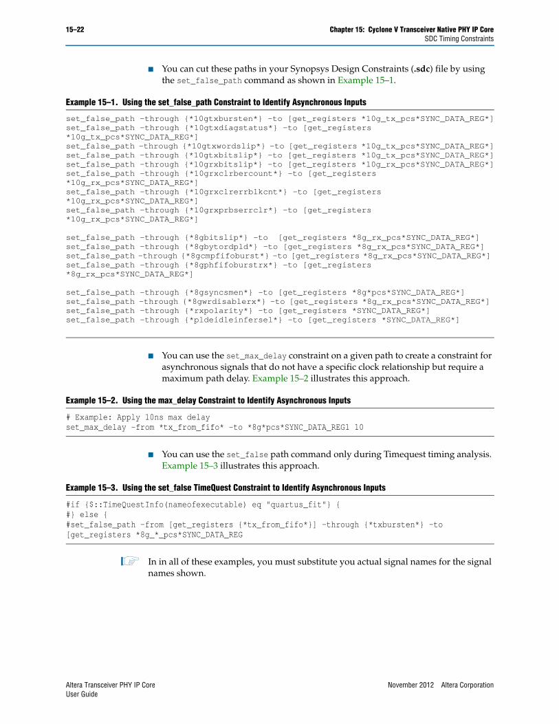
15–22 Chapter 15: Cyclone V Transceiver Native PHY IP CoreSDC Timing Constraints
■ You can cut these paths in your Synopsys Design Constraints (.sdc) file by using the set_false_path command as shown in Example 15–1.
■ You can use the set_max_delay constraint on a given path to create a constraint for asynchronous signals that do not have a specific clock relationship but require a maximum path delay. Example 15–2 illustrates this approach.
■ You can use the set_false path command only during Timequest timing analysis. Example 15–3 illustrates this approach.
1 In in all of these examples, you must substitute you actual signal names for the signal names shown.
Example 15–1. Using the set_false_path Constraint to Identify Asynchronous Inputs
set_false_path -through {*10gtxbursten*} -to [get_registers *10g_tx_pcs*SYNC_DATA_REG*]set_false_path -through {*10gtxdiagstatus*} -to [get_registers *10g_tx_pcs*SYNC_DATA_REG*]set_false_path -through {*10gtxwordslip*} -to [get_registers *10g_tx_pcs*SYNC_DATA_REG*]set_false_path -through {*10gtxbitslip*} -to [get_registers *10g_tx_pcs*SYNC_DATA_REG*]set_false_path -through {*10grxbitslip*} -to [get_registers *10g_rx_pcs*SYNC_DATA_REG*]set_false_path -through {*10grxclrbercount*} -to [get_registers *10g_rx_pcs*SYNC_DATA_REG*] set_false_path -through {*10grxclrerrblkcnt*} -to [get_registers *10g_rx_pcs*SYNC_DATA_REG*] set_false_path -through {*10grxprbserrclr*} -to [get_registers *10g_rx_pcs*SYNC_DATA_REG*]
set_false_path -through {*8gbitslip*} -to [get_registers *8g_rx_pcs*SYNC_DATA_REG*]set_false_path -through {*8gbytordpld*} -to [get_registers *8g_rx_pcs*SYNC_DATA_REG*] set_false_path -through {*8gcmpfifoburst*} -to [get_registers *8g_rx_pcs*SYNC_DATA_REG*] set_false_path -through {*8gphfifoburstrx*} -to [get_registers *8g_rx_pcs*SYNC_DATA_REG*]
set_false_path -through {*8gsyncsmen*} -to [get_registers *8g*pcs*SYNC_DATA_REG*]set_false_path -through {*8gwrdisablerx*} -to [get_registers *8g_rx_pcs*SYNC_DATA_REG*] set_false_path -through {*rxpolarity*} -to [get_registers *SYNC_DATA_REG*]set_false_path -through {*pldeidleinfersel*} -to [get_registers *SYNC_DATA_REG*]
Example 15–2. Using the max_delay Constraint to Identify Asynchronous Inputs
# Example: Apply 10ns max delayset_max_delay -from *tx_from_fifo* -to *8g*pcs*SYNC_DATA_REG1 10
Example 15–3. Using the set_false TimeQuest Constraint to Identify Asynchronous Inputs
#if {$::TimeQuestInfo(nameofexecutable) eq "quartus_fit"} { #} else {#set_false_path -from [get_registers {*tx_from_fifo*}] -through {*txbursten*} -to [get_registers *8g_*_pcs*SYNC_DATA_REG
Altera Transceiver PHY IP Core November 2012 Altera CorporationUser Guide
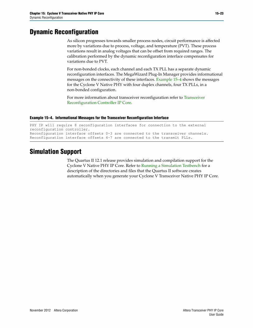
Chapter 15: Cyclone V Transceiver Native PHY IP Core 15–23Dynamic Reconfiguration
Dynamic Reconfiguration As silicon progresses towards smaller process nodes, circuit performance is affected more by variations due to process, voltage, and temperature (PVT). These process variations result in analog voltages that can be offset from required ranges. The calibration performed by the dynamic reconfiguration interface compensates for variations due to PVT.
For non-bonded clocks, each channel and each TX PLL has a separate dynamic reconfiguration interfaces. The MegaWizard Plug-In Manager provides informational messages on the connectivity of these interfaces. Example 15–4 shows the messages for the Cyclone V Native PHY with four duplex channels, four TX PLLs, in a non-bonded configuration.
For more information about transceiver reconfiguration refer to Transceiver Reconfiguration Controller IP Core.
Simulation SupportThe Quartus II 12.1 release provides simulation and compilation support for the Cyclone V Native PHY IP Core. Refer to Running a Simulation Testbench for a description of the directories and files that the Quartus II software creates automatically when you generate your Cyclone V Transceiver Native PHY IP Core.
Example 15–4. Informational Messages for the Transceiver Reconfiguration Interface
PHY IP will require 8 reconfiguration interfaces for connection to the external reconfiguration controller.Reconfiguration interface offsets 0-3 are connected to the transceiver channels.Reconfiguration interface offsets 4–7 are connected to the transmit PLLs.
November 2012 Altera Corporation Altera Transceiver PHY IP CoreUser Guide

15–24 Chapter 15: Cyclone V Transceiver Native PHY IP CoreSimulation Support
Altera Transceiver PHY IP Core November 2012 Altera CorporationUser Guide
November 2012 Altera Corporation
16. Transceiver ReconfigurationController IP Core
The Altera Transceiver Reconfiguration Controller dynamically reconfigures analog settings in Arria V, Cyclone V, and Stratix V devices. Reconfiguration allows you to compensate for variations due to process, voltage, and temperature (PVT) in 28-nm devices. It is required for Arria V, Cyclone V, and Stratix V devices that include transceivers. The reconfiguration functionality available in Arria V and Cyclone V devices is a subset of the functionality available for Stratix V devices. Table 16–1 summarizes the features available for all 28-nm devices.
1 Some of the reconfiguration features not available for Arria V and Cyclone V devices in the current release, may be available in subsequent releases. Arria V and Cyclone V devices do not include ATX PLLs. Stratix V and Arria V GZ devices include ATX PLLs.
f For more information about the features that are available for each device refer to the following device documentation: Dynamic Reconfiguration in Stratix V Devices, Dynamic Reconfiguration in Arria V Devices, and Dynamic Reconfiguration in Cyclone V Devices. These chapters are included in the Stratix V, Arria V, and Cyclone V device handbooks, respectively.
Table 16–1. Device Support for Dynamic Reconfiguration
Area Feature Stratix V Arria V Arria V GZ Cyclone V
Calibration Functions
Offset cancellation v v v vDuty cycle distortion calibration v v v —
ATX PLL calibration v — v —
Analog Features
On-chip signal quality monitoring v — v —
Decision feedback equalization (DFE) v — v —
Adaptive equalization v — v —
Loopback modesPre-CDR reverse serial loopback v v v vPost-CDR reverse serial loopback v v v v
PLL reconfiguration
Reference clock switching (CDR, ATX PLLs, and TX PLLs) v v v vTX PLL connected to a transceiver channel reconfiguration v v v v
Transceiver Channel/PLL Reconfiguration
RX CDR reconfiguration v v v vReconfiguration of PCS blocks v v v vTX PLL switching v — v —
ATX PLL switching v — v —
TX local clock divider reconfiguration (1,2,4,8) v v v vFPGA fabric-transceiver channel data width reconfiguration v v v v
Altera Transceiver PHY IP CoreUser Guide
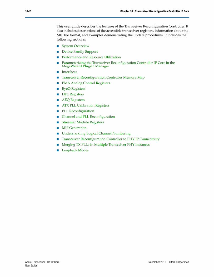
16–2 Chapter 16: Transceiver Reconfiguration Controller IP Core
This user guide describes the features of the Transceiver Reconfiguration Controller. It also includes descriptions of the accessible transceiver registers, information about the MIF file format, and examples demonstrating the update procedures. It includes the following sections:
■ System Overview
■ Device Family Support
■ Performance and Resource Utilization
■ Parameterizing the Transceiver Reconfiguration Controller IP Core in the MegaWizard Plug-In Manager
■ Interfaces
■ Transceiver Reconfiguration Controller Memory Map
■ PMA Analog Control Registers
■ EyeQ Registers
■ DFE Registers
■ AEQ Registers
■ ATX PLL Calibration Registers
■ PLL Reconfiguration
■ Channel and PLL Reconfiguration
■ Streamer Module Registers
■ MIF Generation
■ Understanding Logical Channel Numbering
■ Transceiver Reconfiguration Controller to PHY IP Connectivity
■ Merging TX PLLs In Multiple Transceiver PHY Instances
■ Loopback Modes
Altera Transceiver PHY IP Core November 2012 Altera CorporationUser Guide
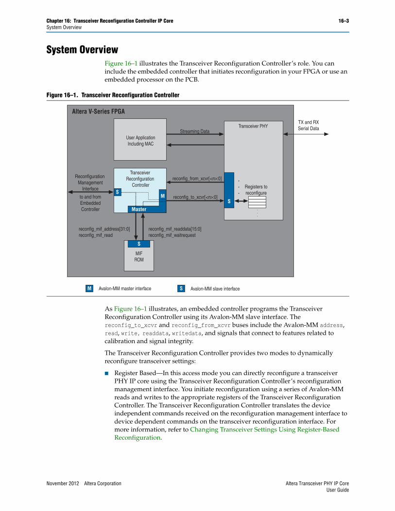
Chapter 16: Transceiver Reconfiguration Controller IP Core 16–3System Overview
System OverviewFigure 16–1 illustrates the Transceiver Reconfiguration Controller’s role. You can include the embedded controller that initiates reconfiguration in your FPGA or use an embedded processor on the PCB.
As Figure 16–1 illustrates, an embedded controller programs the Transceiver Reconfiguration Controller using its Avalon-MM slave interface. The reconfig_to_xcvr and reconfig_from_xcvr buses include the Avalon-MM address, read, write, readdata, writedata, and signals that connect to features related to calibration and signal integrity.
The Transceiver Reconfiguration Controller provides two modes to dynamically reconfigure transceiver settings:
■ Register Based—In this access mode you can directly reconfigure a transceiver PHY IP core using the Transceiver Reconfiguration Controller’s reconfiguration management interface. You initiate reconfiguration using a series of Avalon-MM reads and writes to the appropriate registers of the Transceiver Reconfiguration Controller. The Transceiver Reconfiguration Controller translates the device independent commands received on the reconfiguration management interface to device dependent commands on the transceiver reconfiguration interface. For more information, refer to Changing Transceiver Settings Using Register-Based Reconfiguration.
Figure 16–1. Transceiver Reconfiguration Controller
to and fromEmbeddedController
TX and RXSerial Data
Avalon-MM master interface
Transceiver Reconfiguration
ControllerS
M Avalon-MM slave interfaceS
reconfig_to_xcvr[<n>:0]
reconfig_mif_address[31:0]reconfig_mif_read
Reconfiguration Management
Interface
reconfig_mif_readdata[15:0]reconfig_mif_waitrequest
Streaming Data
reconfig_from_xcvr[<n>:0]
Transceiver PHY
Registers toreconfigure
User ApplicationIncluding MAC
Altera V-Series FPGA
.
.
.
.
.
.
S
MMaster
M
S
MIFROM
November 2012 Altera Corporation Altera Transceiver PHY IP CoreUser Guide
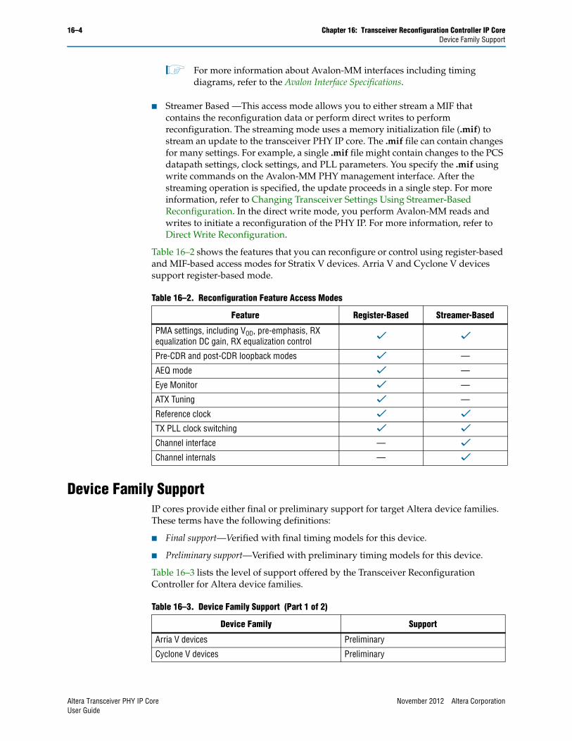
16–4 Chapter 16: Transceiver Reconfiguration Controller IP CoreDevice Family Support
1 For more information about Avalon-MM interfaces including timing diagrams, refer to the Avalon Interface Specifications.
■ Streamer Based —This access mode allows you to either stream a MIF that contains the reconfiguration data or perform direct writes to perform reconfiguration. The streaming mode uses a memory initialization file (.mif) to stream an update to the transceiver PHY IP core. The .mif file can contain changes for many settings. For example, a single .mif file might contain changes to the PCS datapath settings, clock settings, and PLL parameters. You specify the .mif using write commands on the Avalon-MM PHY management interface. After the streaming operation is specified, the update proceeds in a single step. For more information, refer to Changing Transceiver Settings Using Streamer-Based Reconfiguration. In the direct write mode, you perform Avalon-MM reads and writes to initiate a reconfiguration of the PHY IP. For more information, refer to Direct Write Reconfiguration.
Table 16–2 shows the features that you can reconfigure or control using register-based and MIF-based access modes for Stratix V devices. Arria V and Cyclone V devices support register-based mode.
Device Family SupportIP cores provide either final or preliminary support for target Altera device families. These terms have the following definitions:
■ Final support—Verified with final timing models for this device.
■ Preliminary support—Verified with preliminary timing models for this device.
Table 16–3 lists the level of support offered by the Transceiver Reconfiguration Controller for Altera device families.
Table 16–2. Reconfiguration Feature Access Modes
Feature Register-Based Streamer-Based
PMA settings, including VOD, pre-emphasis, RX equalization DC gain, RX equalization control v vPre-CDR and post-CDR loopback modes v —
AEQ mode v —
Eye Monitor v —
ATX Tuning v —
Reference clock v vTX PLL clock switching v vChannel interface — vChannel internals — v
Table 16–3. Device Family Support (Part 1 of 2)
Device Family Support
Arria V devices Preliminary
Cyclone V devices Preliminary
Altera Transceiver PHY IP Core November 2012 Altera CorporationUser Guide
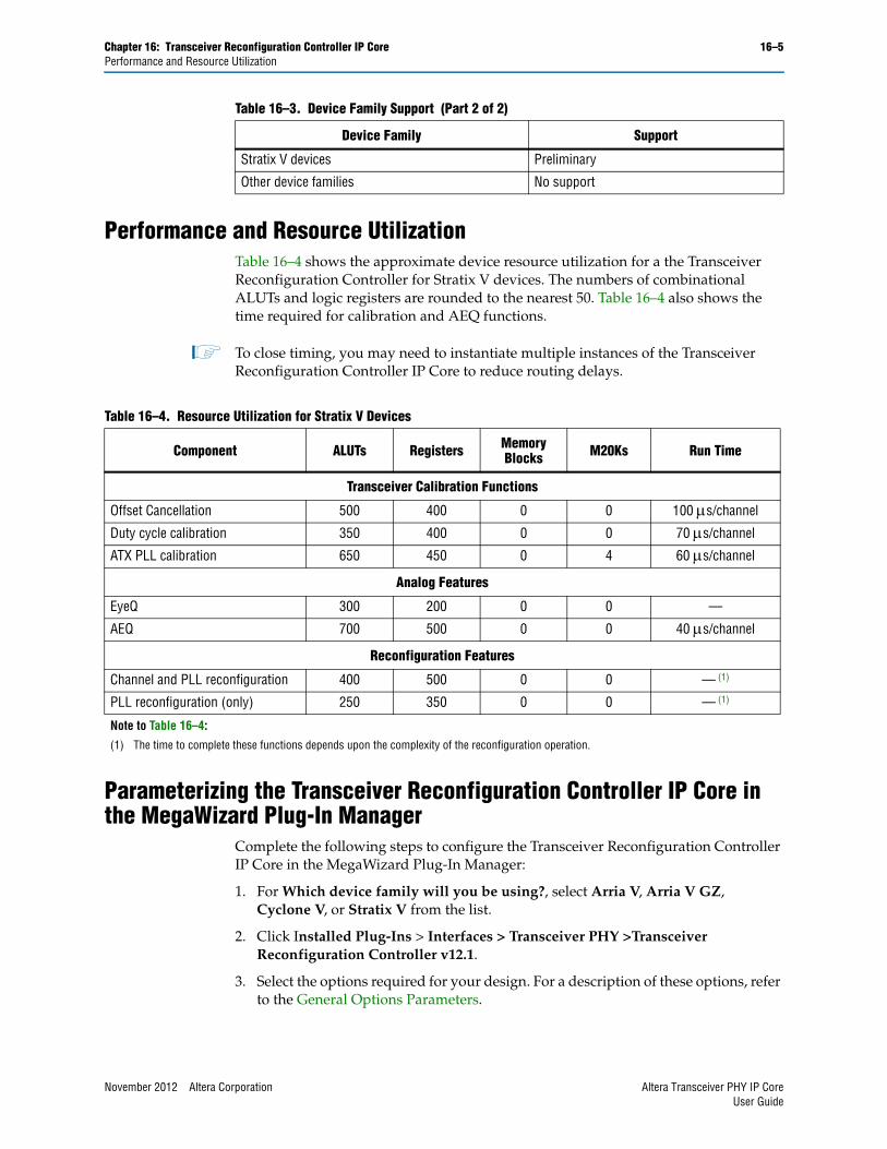
Chapter 16: Transceiver Reconfiguration Controller IP Core 16–5Performance and Resource Utilization
Performance and Resource Utilization Table 16–4 shows the approximate device resource utilization for a the Transceiver Reconfiguration Controller for Stratix V devices. The numbers of combinational ALUTs and logic registers are rounded to the nearest 50. Table 16–4 also shows the time required for calibration and AEQ functions.
1 To close timing, you may need to instantiate multiple instances of the Transceiver Reconfiguration Controller IP Core to reduce routing delays.
Parameterizing the Transceiver Reconfiguration Controller IP Core in the MegaWizard Plug-In Manager
Complete the following steps to configure the Transceiver Reconfiguration Controller IP Core in the MegaWizard Plug-In Manager:
1. For Which device family will you be using?, select Arria V, Arria V GZ, Cyclone V, or Stratix V from the list.
2. Click Installed Plug-Ins > Interfaces > Transceiver PHY >Transceiver Reconfiguration Controller v12.1.
3. Select the options required for your design. For a description of these options, refer to the General Options Parameters.
Stratix V devices Preliminary
Other device families No support
Table 16–3. Device Family Support (Part 2 of 2)
Device Family Support
Table 16–4. Resource Utilization for Stratix V Devices
Component ALUTs Registers Memory Blocks M20Ks Run Time
Transceiver Calibration Functions
Offset Cancellation 500 400 0 0 100 s/channel
Duty cycle calibration 350 400 0 0 70 s/channel
ATX PLL calibration 650 450 0 4 60 s/channel
Analog Features
EyeQ 300 200 0 0 —
AEQ 700 500 0 0 40 s/channel
Reconfiguration Features
Channel and PLL reconfiguration 400 500 0 0 — (1)
PLL reconfiguration (only) 250 350 0 0 — (1)
Note to Table 16–4:
(1) The time to complete these functions depends upon the complexity of the reconfiguration operation.
November 2012 Altera Corporation Altera Transceiver PHY IP CoreUser Guide
16–6 Chapter 16: Transceiver Reconfiguration Controller IP CoreParameterizing the Transceiver Reconfiguration Controller IP Core in Qsys
4. Click Finish to generate your customized Transceiver Reconfiguration Controller PHY IP Core.
Parameterizing the Transceiver Reconfiguration Controller IP Core in Qsys
Complete the following steps to configure the Transceiver Reconfiguration Controller IP Core in Qsys:
1. On the Project Settings tab, select Arria V, Arria V GZ, Cyclone V, or Stratix V from the list.
2. On the Component Library tab, type the following text string in the search box:
reconfigrQsys filters the component library and shows all components matching the text string you entered.
3. Click Transceiver Reconfiguration Controller and then click +Add.
4. Select the options required for your design. For a description of these options, refer to the General Options Parameters.
5. Click Finish to generate your customized Transceiver Reconfiguration Controller PHY IP Core.
General Options ParametersTable 16–5 lists the available options.
Table 16–5. General Options (Part 1 of 2)
Name Value Description
Device family
Arria VArria V GZCyclone VStratix V
Specifies the device family. The reconfiguration functions available for Arria V and Cyclone V devices are a subset of those available for Stratix V devices. Refer to Table 16–1 on page 16–1 for more information about available functions.
Interface Bundles
Number of reconfiguration interfaces <IF>
Specifies the total number of reconfiguration interfaces that connect to the Transceiver Reconfiguration Controller. There is one interface for each channel and TX PLL.
When you specify the parameters for a transceiver PHY, the message window displays the number of interfaces required.
Optional interface grouping <Grp1>,<Grp2>,<Grp3>
Specifies the grouping of reconfiguration interfaces as a comma-separated list with each integer indicating the total number of reconfiguration interfaces that are connected to a transceiver PHY instance. Leave this entry blank if all reconfiguration interfaces connect to the same transceiver PHY instance.
Refer to Understanding Logical Channel Numbering for more information about grouping interfaces.
Altera Transceiver PHY IP Core November 2012 Altera CorporationUser Guide
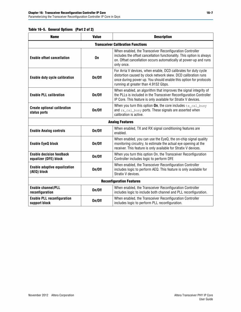
Chapter 16: Transceiver Reconfiguration Controller IP Core 16–7Parameterizing the Transceiver Reconfiguration Controller IP Core in Qsys
Transceiver Calibration Functions
Enable offset cancellation On
When enabled, the Transceiver Reconfiguration Controller includes the offset cancellation functionality. This option is always on. Offset cancellation occurs automatically at power-up and runs only once.
Enable duty cycle calibration On/Off
For Arria V devices, when enable, DCD calibrates for duty cycle distortion caused by clock network skew. DCD calibration runs once during power up. You should enable this option for protocols running at greater than 4.9152 Gbps.
Enable PLL calibration On/OffWhen enabled, an algorithm that improves the signal integrity of the PLLs is included in the Transceiver Reconfiguration Controller IP Core. This feature is only available for Stratix V devices.
Create optional calibration status ports On/Off
When you turn this option On, the core includes tx_cal_busy and rx_cal_busy ports. These signals are asserted when calibration is active.
Analog Features
Enable Analog controls On/Off When enabled, TX and RX signal conditioning features are enabled.
Enable EyeQ block On/OffWhen enabled, you can use the EyeQ, the on-chip signal quality monitoring circuitry, to estimate the actual eye opening at the receiver. This feature is only available for Stratix V devices.
Enable decision feedback equalizer (DFE) block On/Off When you turn this option On, the Transceiver Reconfiguration
Controller includes logic to perform DFE
Enable adaptive equalization (AEQ) block On/Off
When enabled, the Transceiver Reconfiguration Controller includes logic to perform AEQ. This feature is only available for Stratix V devices.
Reconfiguration Features
Enable channel/PLL reconfiguration On/Off When enabled, the Transceiver Reconfiguration Controller
includes logic to include both channel and PLL reconfiguration.
Enable PLL reconfiguration support block On/Off When enabled, the Transceiver Reconfiguration Controller
includes logic to perform PLL reconfiguration.
Table 16–5. General Options (Part 2 of 2)
Name Value Description
November 2012 Altera Corporation Altera Transceiver PHY IP CoreUser Guide
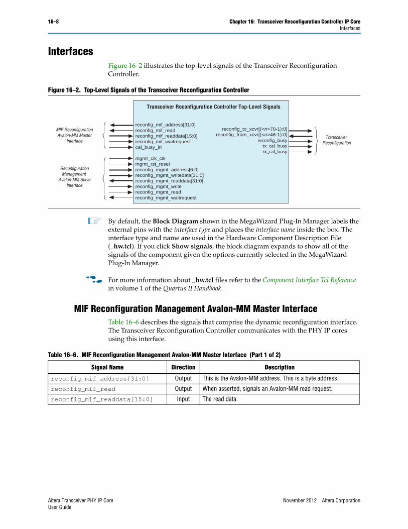
16–8 Chapter 16: Transceiver Reconfiguration Controller IP CoreInterfaces
InterfacesFigure 16–2 illustrates the top-level signals of the Transceiver Reconfiguration Controller.
1 By default, the Block Diagram shown in the MegaWizard Plug-In Manager labels the external pins with the interface type and places the interface name inside the box. The interface type and name are used in the Hardware Component Description File (_hw.tcl). If you click Show signals, the block diagram expands to show all of the signals of the component given the options currently selected in the MegaWizard Plug-In Manager.
f For more information about _hw.tcl files refer to the Component Interface Tcl Reference in volume 1 of the Quartus II Handbook.
MIF Reconfiguration Management Avalon-MM Master InterfaceTable 16–6 describes the signals that comprise the dynamic reconfiguration interface. The Transceiver Reconfiguration Controller communicates with the PHY IP cores using this interface.
Figure 16–2. Top-Level Signals of the Transceiver Reconfiguration Controller
Transceiver Reconfiguration Controller Top-Level Signals
ReconfigurationManagement
Avalon-MM SlaveInterface
MIF ReconfigurationAvalon-MM Master
InterfaceTransceiver
Reconfiguration
reconfig_mif_address[31:0]reconfig_mif_readreconfig_mif_readdata[15:0]reconfig_mif_waitrequestcal_busy_in
mgmt_clk_clkmgmt_rst_resetreconfig_mgmt_address[6:0]reconfig_mgmt_writedata[31:0]reconfig_mgmt_readdata[31:0]reconfig_mgmt_writereconfig_mgmt_readreconfig_mgmt_waitrequest
reconfig_to_xcvr[(<n>70-1):0]reconfig_from_xcvr[(<n>46-1):0]
reconfig_busytx_cal_busyrx_cal_busy
Table 16–6. MIF Reconfiguration Management Avalon-MM Master Interface (Part 1 of 2)
Signal Name Direction Description
reconfig_mif_address[31:0] Output This is the Avalon-MM address. This is a byte address.
reconfig_mif_read Output When asserted, signals an Avalon-MM read request.
reconfig_mif_readdata[15:0] Input The read data.
Altera Transceiver PHY IP Core November 2012 Altera CorporationUser Guide
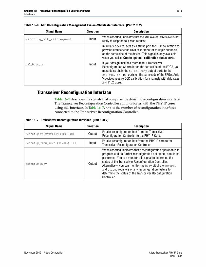
Chapter 16: Transceiver Reconfiguration Controller IP Core 16–9Interfaces
Transceiver Reconfiguration InterfaceTable 16–7 describes the signals that comprise the dynamic reconfiguration interface. The Transceiver Reconfiguration Controller communicates with the PHY IP cores using this interface. In Table 16–7, <n> is the number of reconfiguration interfaces connected to the Transceiver Reconfiguration Controller.
reconfig_mif_waitrequest Input When asserted, indicates that the MIF Avalon-MM slave is not ready to respond to a read request.
cal_busy_in Input
In Arria V devices, acts as a status port for DCD calibration to prevent simultaneous DCD calibration for multiple channels on the same side of the device. This signal is only available when you select Create optional calibration status ports.
If your design includes more than 1 Transceiver Reconfiguration Controller on the same side of the FPGA, you must daisy chain the tx_cal_busy output ports to the cal_busy_in input ports on the same side of the FPGA. Arria V devices require DCD calibration for channels with data rates 4.9152 Gbps.
Table 16–6. MIF Reconfiguration Management Avalon-MM Master Interface (Part 2 of 2)
Signal Name Direction Description
Table 16–7. Transceiver Reconfiguration Interface (Part 1 of 2)
Signal Name Direction Description
reconfig_to_xcvr[(<n>×70)-1:0] Output Parallel reconfiguration bus from the Transceiver Reconfiguration Controller to the PHY IP Core.
reconfig_from_xcvr[(<n>×46)-1:0] Input Parallel reconfiguration bus from the PHY IP core to the Transceiver Reconfiguration Controller.
reconfig_busy Output
When asserted, indicates that a reconfiguration operation is in progress and no further reconfiguration operations should be performed. You can monitor this signal to determine the status of the Transceiver Reconfiguration Controller. Alternatively, you can monitor the busy bit of the control and status registers of any reconfiguration feature to determine the status of the Transceiver Reconfiguration Controller.
November 2012 Altera Corporation Altera Transceiver PHY IP CoreUser Guide
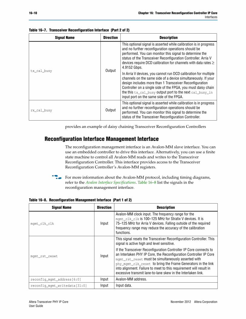
16–10 Chapter 16: Transceiver Reconfiguration Controller IP CoreInterfaces
provides an example of daisy chaining Transceiver Reconfiguration Controllers
Reconfiguration Interface Management InterfaceThe reconfiguration management interface is an Avalon-MM slave interface. You can use an embedded controller to drive this interface. Alternatively, you can use a finite state machine to control all Avalon-MM reads and writes to the Transceiver Reconfiguration Controller. This interface provides access to the Transceiver Reconfiguration Controller’s Avalon-MM registers.
f For more information about the Avalon-MM protocol, including timing diagrams, refer to the Avalon Interface Specifications. Table 16–8 list the signals in the reconfiguration management interface.
tx_cal_busy Output
This optional signal is asserted while calibration is in progress and no further reconfiguration operations should be performed. You can monitor this signal to determine the status of the Transceiver Reconfiguration Controller. Arria V devices require DCD calibration for channels with data rates 4.9152 Gbps.
In Arria V devices, you cannot run DCD calibration for multiple channels on the same side of a device simultaneously. If your design includes more than 1 Transceiver Reconfiguration Controller on a single side of the FPGA, you must daisy chain the this tx_cal_busy output port to the next cal_busy_in input port on the same side of the FPGA.
rx_cal_busy Output
This optional signal is asserted while calibration is in progress and no further reconfiguration operations should be performed. You can monitor this signal to determine the status of the Transceiver Reconfiguration Controller.
Table 16–7. Transceiver Reconfiguration Interface (Part 2 of 2)
Signal Name Direction Description
Table 16–8. Reconfiguration Management Interface (Part 1 of 2)
Signal Name Direction Description
mgmt_clk_clk Input
Avalon-MM clock input. The frequency range for the mgmt_clk_clk is 100–125 MHz for Stratix V devices. It is 75–125 MHz for Arria V devices. Falling outside of the required frequency range may reduce the accuracy of the calibration functions.
mgmt_rst_reset Input
This signal resets the Transceiver Reconfiguration Controller. This signal is active high and level sensitive.
If the Transceiver Reconfiguration Controller IP Core connects to an Interlaken PHY IP Core, the Reconfiguration Controller IP Core mgmt_rst_reset must be simultaneously asserted with phy_mgmt_clk_reset to bring the Frame Generators in the link into alignment. Failure to meet to this requirement will result in excessive transmit lane-to-lane skew in the Interlaken link.
reconfig_mgmt_address[6:0] Input Avalon-MM address.
reconfig_mgmt_writedata[31:0] Input Input data.
Altera Transceiver PHY IP Core November 2012 Altera CorporationUser Guide
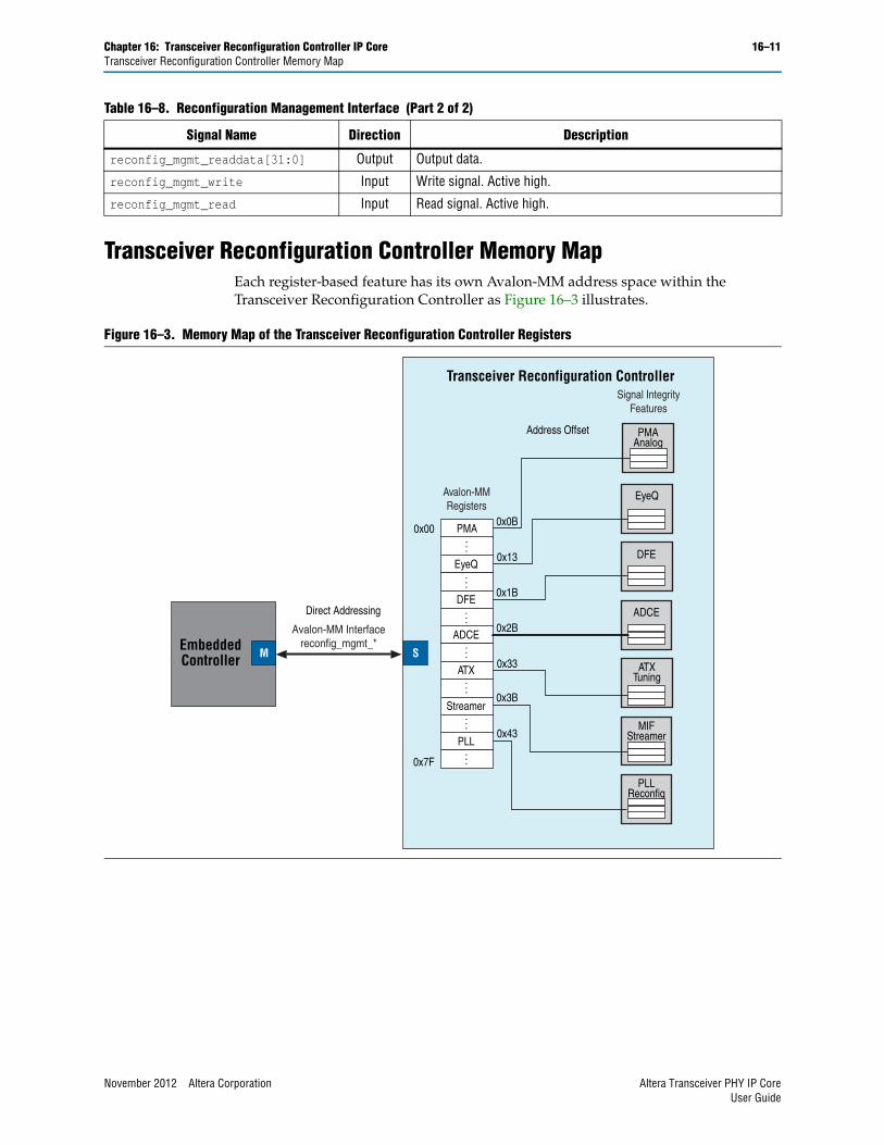
Chapter 16: Transceiver Reconfiguration Controller IP Core 16–11Transceiver Reconfiguration Controller Memory Map
Transceiver Reconfiguration Controller Memory MapEach register-based feature has its own Avalon-MM address space within the Transceiver Reconfiguration Controller as Figure 16–3 illustrates.
reconfig_mgmt_readdata[31:0] Output Output data.
reconfig_mgmt_write Input Write signal. Active high.
reconfig_mgmt_read Input Read signal. Active high.
Table 16–8. Reconfiguration Management Interface (Part 2 of 2)
Signal Name Direction Description
Figure 16–3. Memory Map of the Transceiver Reconfiguration Controller Registers
Direct Addressing
Address Offset
0x00
0x13
0x0B
0x1B
0x2B
0x33
0x3B
0x43
0x7F
Transceiver Reconfiguration Controller
Avalon-MM Interfacereconfig_mgmt_*
Avalon-MMRegisters
Signal IntegrityFeatures
DFE
ADCE
ATXTuning
MIFStreamer
PLLReconfig
EyeQ
PMAAnalog
EyeQ
. . .
DFE
. . .
PMA
ADCE
. . .
ATX
. . .
Streamer
. . .
PLL
. . .
SMEmbeddedController
. . .
November 2012 Altera Corporation Altera Transceiver PHY IP CoreUser Guide
16–12 Chapter 16: Transceiver Reconfiguration Controller IP CoreTransceiver Reconfiguration Controller Calibration Functions
Table 16–9 lists the address range for the Transceiver Reconfiguration Controller and the reconfiguration and signal integrity modules. It provides links to the sections describing the registers in each module.
Transceiver Reconfiguration Controller Calibration FunctionsThe Transceiver Reconfiguration Controller supports various calibration functions to enhance the performance and operation of any connected transceiver PHY IP core. Refer to Resource Utilization for Stratix V Devices for the resource utilization of these calibration functions.
Offset CancellationThe offset cancellation function adjusts the offsets within the RX PMA and the CDR parameters for process variations to achieve optimal performance in Stratix V devices. Offset cancellation runs only once upon power-up. The RX buffers are unavailable while this function is running. This calibration feature is run automatically and enabled by default. Arria V and Cyclone V devices do not require offset cancellation for the RX buffer.
Duty Cycle CalibrationThe TX clocks generated by the CMU and travel across the clock network may introduce duty cycle distortion (DCD). DCD calibration function reduces this distortion. DCD runs once during device power up. Altera recommends that you turn on the DCD for transceiver applications that operate at 4.9152 Gbps or higher in Arria V devices.
Auxiliary Transmit (ATX) PLL CalibrationATX calibration tunes the parameters of the ATX PLL for optimal performance. This function runs once after power up. You can rerun this function by writing into the appropriate memory-mapped registers.
The RX buffer is unavailable while this function is running. You should run the ATX calibration after reconfiguring the PLL. You may need to rerun ATX calibration if you reset an ATX PLL and it does not lock after the specified lock time.
For more information about the Auxiliary Transmit (ATX) PLL Calibration refer to ATX PLL Calibration Registers.
Table 16–9. Transceiver Reconfiguration Controller Address Map
Address Link
7’h08–7’h0C PMA Analog Control Registers
7’h10–7’h14 EyeQ Registers
7’h18–7’h1C DFE Registers
7’h28–7’h2C AEQ Registers
7’h30–7’h34 ATX PLL Calibration Registers
7’h38–7’h3C Streamer Module Registers
7’h40–7’h44 PLL Reconfiguration
Altera Transceiver PHY IP Core November 2012 Altera CorporationUser Guide
Chapter 16: Transceiver Reconfiguration Controller IP Core 16–13PMA Analog Control Registers
Refer to the Parameterizing the Transceiver Reconfiguration Controller IP Core in the MegaWizard Plug-In Manager section for information about how to enabled these functions.
PMA Analog Control RegistersYou can use the Transceiver Reconfiguration Controller to reconfigure the following analog controls:
■ Differential output voltage (VOD)
■ Pre-emphasis taps
■ Receiver equalization control
■ Receiver equalization DC gain
■ Reverse serial loopback
Table 16–10 lists the memory-mapped PMA analog registers that you can access using the reconfiguration management interface.
1 All undefined register bits are reserved.
.
Table 16–10. PMA Analog Registers
Recon-fig Addr
Bits R/W Register Name Description
7’h08 [9:0] RW logical channel number
The logical channel number. Must be specified when performing dynamic updates. The Transceiver Reconfiguration Controller maps the logical address to the physical address.
7’h09 [9:0] R physical channel addressThe physical channel address. The Transceiver Reconfiguration Controller maps the logical address to the physical address.
7’h0A
[9] R
control and status
Error. When asserted, indicates an error. This bit is asserted if any of the following conditions occur:
■ The channel address is invalid.
■ The PHY address is invalid.
■ The PMA offset is invalid.
[8] R Busy. When asserted, indicates that a reconfiguration operation is in progress.
[1] W Read. Writing a 1 to this bit triggers a read operation.
[0] W Write. Writing a 1 to this bit triggers a write operation.
7’h0B [5:0] RW pma offsetSpecifies the offset of the PMA analog setting to be reconfigured. Table 16–11 describes the valid offset values.
7’h0C [6:0] RW dataReconfiguration data for the PMA analog settings. Refer to Table 16–11 for valid data values.
November 2012 Altera Corporation Altera Transceiver PHY IP CoreUser Guide
16–14 Chapter 16: Transceiver Reconfiguration Controller IP CoreEyeQ Registers
f Refer to the Arria V Device Datasheet, the Cyclone V Device Datasheet, or the Stratix V Device Datasheet for more information about the electrical characteristics of each device. The final values are currently pending full characterization of the silicon.
1 All undefined register bits are reserved and must be set to 0.
Refer to Changing Transceiver Settings Using Register-Based Reconfiguration and Changing Transceiver Settings Using Streamer-Based Reconfiguration for the procedures you can use to update PMA settings.
f Refer to Application Note 645: Dynamic Reconfiguration of PMA Controls in Stratix V Devices for an example demonstrating the use of the Transceiver Reconfiguration Controller.
EyeQ RegistersEyeQ is a debug and diagnostic tool that analyzes the incoming data, including the receiver’s gain, noise level, and jitter after the receive buffer. EyeQ is only available for Stratix V devices.
Table 16–11. PMA Offsets and Values
Offset Bits R/W Register Name Description
0x0 [5:0] RW VODVOD. The following encodings are defined:
■ 6’b000000:6’b111111:0–63
0x1 [4:0] RW Pre-emphasis pre-tap
The following encodings are defined:
■ 5’b00000–5’b10000: 0
■ 5’b00001–5’b01111: -15 to -1
■ 5’b10001–5b’11111: 1 to 15
0x2 [4:0] RW Pre-emphasis first post-tapThe following encodings are defined:
■ 5’b00000–5’b11111: 0–31
0x3 [4:0] RW Pre-emphasis second post-tap
The following encodings are defined:
■ 5’b00000–5’b10000: 0
■ 5’b00001–5’b01111: -15 to -1
■ 5’b10001–5b’11111: 1 to 15
0x10 [2:0] RW RX equalization DC gainThe following encodings are defined:
■ 3’b000–3b’111:0–4
0x11 [3:0] WO RX equalization controlThe following encodings are defined:
■ 4’b0000–4’b1111: 0–15
0x20 [0] WOPre-CDR Reverse Serial Loopback
Writing a 1 to this bit enables reverse serial loopback. Writing a 0 disables pre-CDR reverse serial loopback.
0x21 [0] WOPost-CDR Reverse Serial Loopback
Writing a 1 to this bit enables post-CDR reverse serial loopback. Writing a 0 disables post-CDR reverse serial loopback.
Altera Transceiver PHY IP Core November 2012 Altera CorporationUser Guide
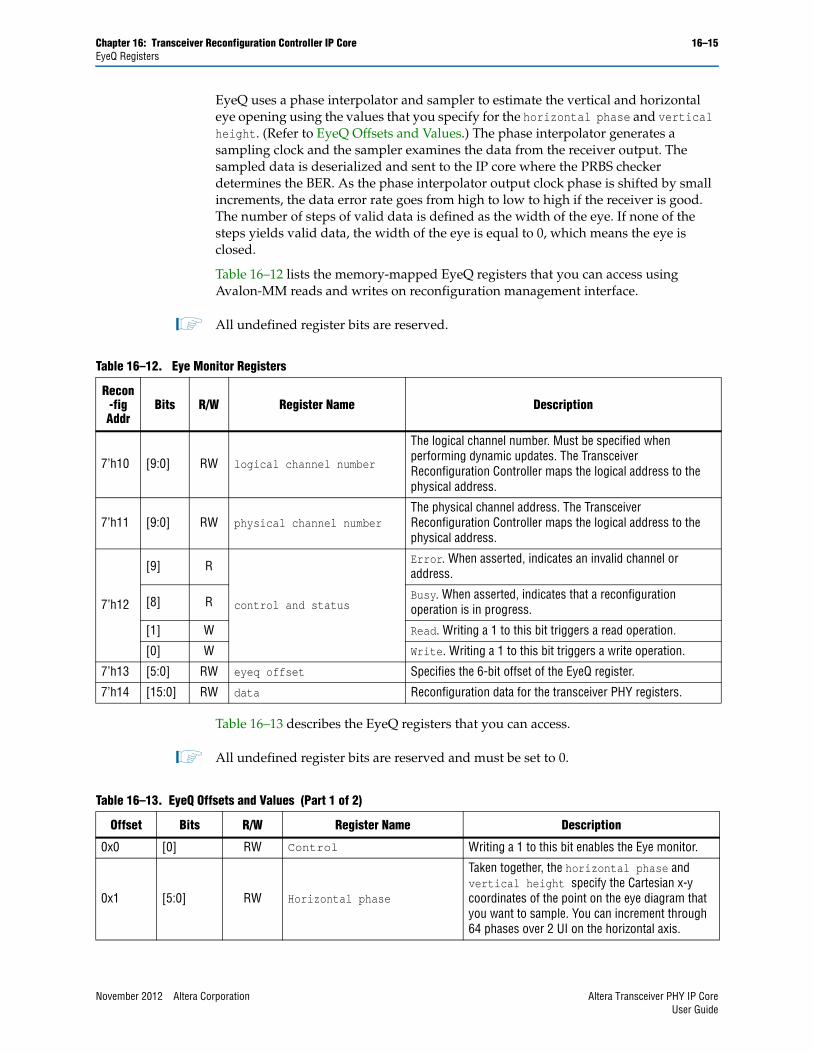
Chapter 16: Transceiver Reconfiguration Controller IP Core 16–15EyeQ Registers
EyeQ uses a phase interpolator and sampler to estimate the vertical and horizontal eye opening using the values that you specify for the horizontal phase and vertical height. (Refer to EyeQ Offsets and Values.) The phase interpolator generates a sampling clock and the sampler examines the data from the receiver output. The sampled data is deserialized and sent to the IP core where the PRBS checker determines the BER. As the phase interpolator output clock phase is shifted by small increments, the data error rate goes from high to low to high if the receiver is good. The number of steps of valid data is defined as the width of the eye. If none of the steps yields valid data, the width of the eye is equal to 0, which means the eye is closed.
Table 16–12 lists the memory-mapped EyeQ registers that you can access using Avalon-MM reads and writes on reconfiguration management interface.
1 All undefined register bits are reserved.
Table 16–13 describes the EyeQ registers that you can access.
1 All undefined register bits are reserved and must be set to 0.
Table 16–12. Eye Monitor Registers
Recon-fig Addr
Bits R/W Register Name Description
7’h10 [9:0] RW logical channel number
The logical channel number. Must be specified when performing dynamic updates. The Transceiver Reconfiguration Controller maps the logical address to the physical address.
7’h11 [9:0] RW physical channel numberThe physical channel address. The Transceiver Reconfiguration Controller maps the logical address to the physical address.
7’h12
[9] R
control and status
Error. When asserted, indicates an invalid channel or address.
[8] R Busy. When asserted, indicates that a reconfiguration operation is in progress.
[1] W Read. Writing a 1 to this bit triggers a read operation.
[0] W Write. Writing a 1 to this bit triggers a write operation.
7’h13 [5:0] RW eyeq offset Specifies the 6-bit offset of the EyeQ register.
7’h14 [15:0] RW data Reconfiguration data for the transceiver PHY registers.
Table 16–13. EyeQ Offsets and Values (Part 1 of 2)
Offset Bits R/W Register Name Description
0x0 [0] RW Control Writing a 1 to this bit enables the Eye monitor.
0x1 [5:0] RW Horizontal phase
Taken together, the horizontal phase and vertical height specify the Cartesian x-y coordinates of the point on the eye diagram that you want to sample. You can increment through 64 phases over 2 UI on the horizontal axis.
November 2012 Altera Corporation Altera Transceiver PHY IP CoreUser Guide
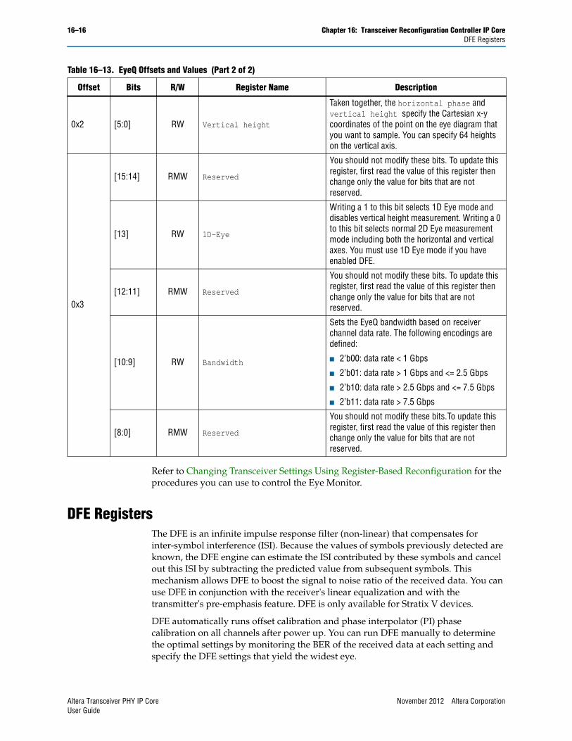
16–16 Chapter 16: Transceiver Reconfiguration Controller IP CoreDFE Registers
Refer to Changing Transceiver Settings Using Register-Based Reconfiguration for the procedures you can use to control the Eye Monitor.
DFE RegistersThe DFE is an infinite impulse response filter (non-linear) that compensates for inter-symbol interference (ISI). Because the values of symbols previously detected are known, the DFE engine can estimate the ISI contributed by these symbols and cancel out this ISI by subtracting the predicted value from subsequent symbols. This mechanism allows DFE to boost the signal to noise ratio of the received data. You can use DFE in conjunction with the receiver's linear equalization and with the transmitter's pre-emphasis feature. DFE is only available for Stratix V devices.
DFE automatically runs offset calibration and phase interpolator (PI) phase calibration on all channels after power up. You can run DFE manually to determine the optimal settings by monitoring the BER of the received data at each setting and specify the DFE settings that yield the widest eye.
0x2 [5:0] RW Vertical height
Taken together, the horizontal phase and vertical height specify the Cartesian x-y coordinates of the point on the eye diagram that you want to sample. You can specify 64 heights on the vertical axis.
0x3
[15:14] RMW Reserved
You should not modify these bits. To update this register, first read the value of this register then change only the value for bits that are not reserved.
[13] RW 1D-Eye
Writing a 1 to this bit selects 1D Eye mode and disables vertical height measurement. Writing a 0 to this bit selects normal 2D Eye measurement mode including both the horizontal and vertical axes. You must use 1D Eye mode if you have enabled DFE.
[12:11] RMW Reserved
You should not modify these bits. To update this register, first read the value of this register then change only the value for bits that are not reserved.
[10:9] RW Bandwidth
Sets the EyeQ bandwidth based on receiver channel data rate. The following encodings are defined:
■ 2’b00: data rate < 1 Gbps
■ 2’b01: data rate > 1 Gbps and <= 2.5 Gbps
■ 2’b10: data rate > 2.5 Gbps and <= 7.5 Gbps
■ 2’b11: data rate > 7.5 Gbps
[8:0] RMW Reserved
You should not modify these bits.To update this register, first read the value of this register then change only the value for bits that are not reserved.
Table 16–13. EyeQ Offsets and Values (Part 2 of 2)
Offset Bits R/W Register Name Description
Altera Transceiver PHY IP Core November 2012 Altera CorporationUser Guide
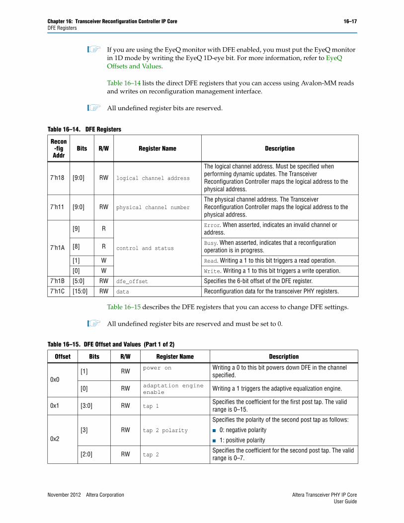
Chapter 16: Transceiver Reconfiguration Controller IP Core 16–17DFE Registers
1 If you are using the EyeQ monitor with DFE enabled, you must put the EyeQ monitor in 1D mode by writing the EyeQ 1D-eye bit. For more information, refer to EyeQ Offsets and Values.
Table 16–14 lists the direct DFE registers that you can access using Avalon-MM reads and writes on reconfiguration management interface.
1 All undefined register bits are reserved.
Table 16–15 describes the DFE registers that you can access to change DFE settings.
1 All undefined register bits are reserved and must be set to 0.
Table 16–14. DFE Registers
Recon-fig Addr
Bits R/W Register Name Description
7’h18 [9:0] RW logical channel address
The logical channel address. Must be specified when performing dynamic updates. The Transceiver Reconfiguration Controller maps the logical address to the physical address.
7’h11 [9:0] RW physical channel numberThe physical channel address. The Transceiver Reconfiguration Controller maps the logical address to the physical address.
7’h1A
[9] R
control and status
Error. When asserted, indicates an invalid channel or address.
[8] R Busy. When asserted, indicates that a reconfiguration operation is in progress.
[1] W Read. Writing a 1 to this bit triggers a read operation.
[0] W Write. Writing a 1 to this bit triggers a write operation.
7’h1B [5:0] RW dfe_offset Specifies the 6-bit offset of the DFE register.
7’h1C [15:0] RW data Reconfiguration data for the transceiver PHY registers.
Table 16–15. DFE Offset and Values (Part 1 of 2)
Offset Bits R/W Register Name Description
0x0[1] RW
power on Writing a 0 to this bit powers down DFE in the channel specified.
[0] RW adaptation engine enable
Writing a 1 triggers the adaptive equalization engine.
0x1 [3:0] RW tap 1Specifies the coefficient for the first post tap. The valid range is 0–15.
0x2[3] RW tap 2 polarity
Specifies the polarity of the second post tap as follows:
■ 0: negative polarity
■ 1: positive polarity
[2:0] RW tap 2Specifies the coefficient for the second post tap. The valid range is 0–7.
November 2012 Altera Corporation Altera Transceiver PHY IP CoreUser Guide
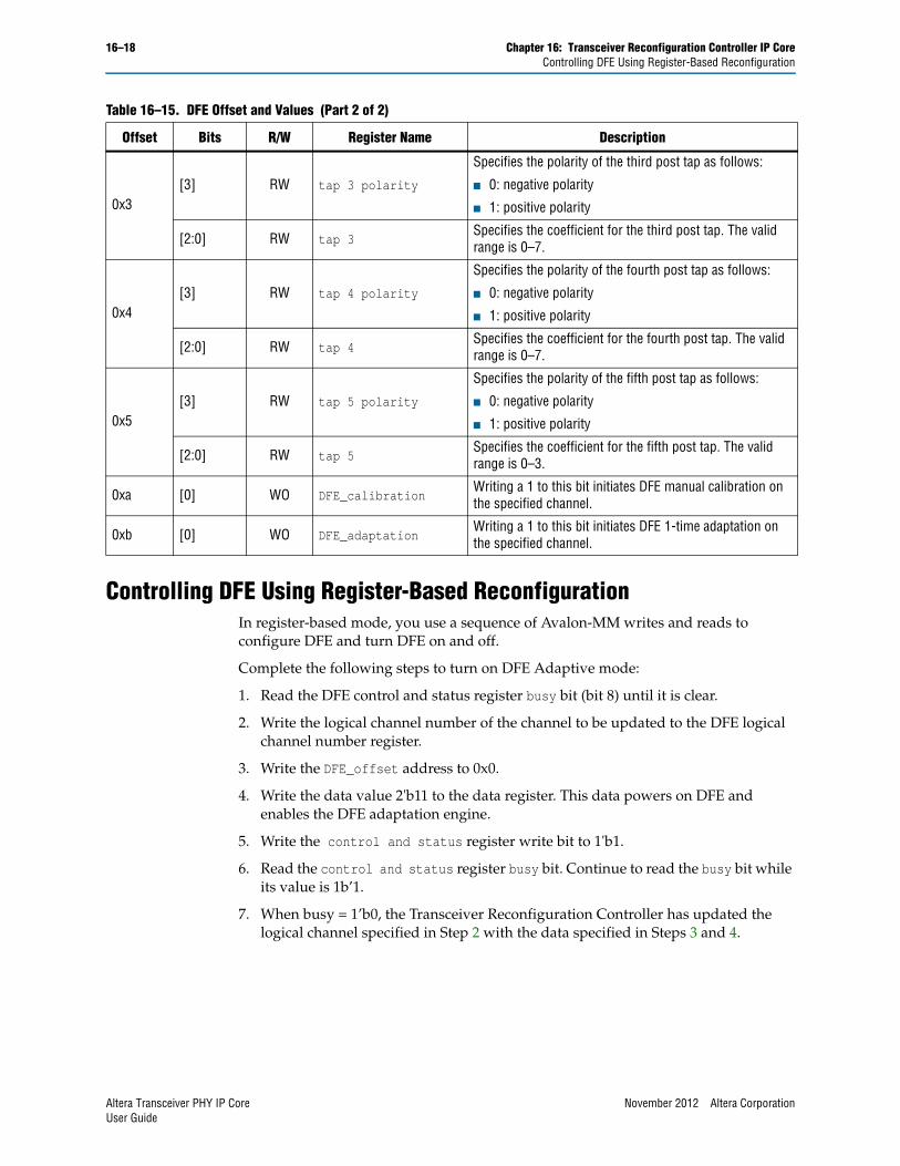
16–18 Chapter 16: Transceiver Reconfiguration Controller IP CoreControlling DFE Using Register-Based Reconfiguration
Controlling DFE Using Register-Based ReconfigurationIn register-based mode, you use a sequence of Avalon-MM writes and reads to configure DFE and turn DFE on and off.
Complete the following steps to turn on DFE Adaptive mode:
1. Read the DFE control and status register busy bit (bit 8) until it is clear.
2. Write the logical channel number of the channel to be updated to the DFE logical channel number register.
3. Write the DFE_offset address to 0x0.
4. Write the data value 2'b11 to the data register. This data powers on DFE and enables the DFE adaptation engine.
5. Write the control and status register write bit to 1'b1.
6. Read the control and status register busy bit. Continue to read the busy bit while its value is 1b’1.
7. When busy = 1’b0, the Transceiver Reconfiguration Controller has updated the logical channel specified in Step 2 with the data specified in Steps 3 and 4.
0x3[3] RW tap 3 polarity
Specifies the polarity of the third post tap as follows:
■ 0: negative polarity
■ 1: positive polarity
[2:0] RW tap 3Specifies the coefficient for the third post tap. The valid range is 0–7.
0x4[3] RW tap 4 polarity
Specifies the polarity of the fourth post tap as follows:
■ 0: negative polarity
■ 1: positive polarity
[2:0] RW tap 4Specifies the coefficient for the fourth post tap. The valid range is 0–7.
0x5[3] RW tap 5 polarity
Specifies the polarity of the fifth post tap as follows:
■ 0: negative polarity
■ 1: positive polarity
[2:0] RW tap 5Specifies the coefficient for the fifth post tap. The valid range is 0–3.
0xa [0] WO DFE_calibrationWriting a 1 to this bit initiates DFE manual calibration on the specified channel.
0xb [0] WO DFE_adaptationWriting a 1 to this bit initiates DFE 1-time adaptation on the specified channel.
Table 16–15. DFE Offset and Values (Part 2 of 2)
Offset Bits R/W Register Name Description
Altera Transceiver PHY IP Core November 2012 Altera CorporationUser Guide
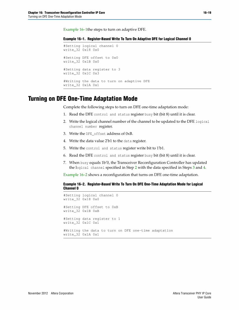
Chapter 16: Transceiver Reconfiguration Controller IP Core 16–19Turning on DFE One-Time Adaptation Mode
Example 16–1the steps to turn on adaptive DFE.
Turning on DFE One-Time Adaptation ModeComplete the following steps to turn on DFE one-time adaptation mode:
1. Read the DFE control and status register busy bit (bit 8) until it is clear.
2. Write the logical channel number of the channel to be updated to the DFE logical channel number register.
3. Write the DFE_offset address of 0xB.
4. Write the data value 2'b1 to the data register.
5. Write the control and status register write bit to 1'b1.
6. Read the DFE control and status register busy bit (bit 8) until it is clear.
7. When busy equals 1b’0, the Transceiver Reconfiguration Controller has updated the logical channel specified in Step 2 with the data specified in Steps 3 and 4.
Example 16–2 shows a reconfiguration that turns on DFE one-time adaptation.
Example 16–1. Register-Based Write To Turn On Adaptive DFE for Logical Channel 0
#Setting logical channel 0write_32 0x18 0x0
#Setting DFE offset to 0x0write_32 0x1B 0x0
#Setting data register to 3write_32 0x1C 0x3
#Writing the data to turn on adaptive DFEwrite_32 0x1A 0x1
Example 16–2. Register-Based Write To Turn On DFE One-Time Adaptation Mode for Logical Channel 0
#Setting logical channel 0write_32 0x18 0x0 #Setting DFE offset to 0xBwrite_32 0x1B 0xB #Setting data register to 1write_32 0x1C 0x1 #Writing the data to turn on DFE one-time adaptationwrite_32 0x1A 0x1
November 2012 Altera Corporation Altera Transceiver PHY IP CoreUser Guide
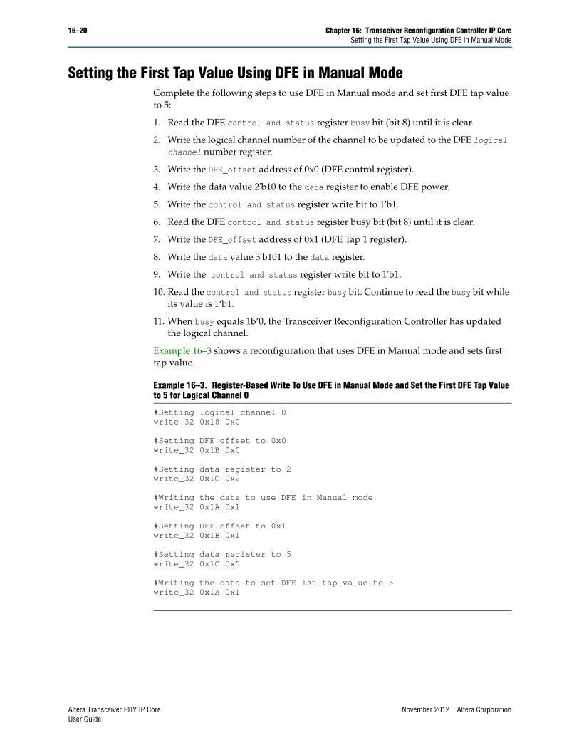
16–20 Chapter 16: Transceiver Reconfiguration Controller IP CoreSetting the First Tap Value Using DFE in Manual Mode
Setting the First Tap Value Using DFE in Manual ModeComplete the following steps to use DFE in Manual mode and set first DFE tap value to 5:
1. Read the DFE control and status register busy bit (bit 8) until it is clear.
2. Write the logical channel number of the channel to be updated to the DFE logical channel number register.
3. Write the DFE_offset address of 0x0 (DFE control register).
4. Write the data value 2'b10 to the data register to enable DFE power.
5. Write the control and status register write bit to 1'b1.
6. Read the DFE control and status register busy bit (bit 8) until it is clear.
7. Write the DFE_offset address of 0x1 (DFE Tap 1 register).
8. Write the data value 3'b101 to the data register.
9. Write the control and status register write bit to 1'b1.
10. Read the control and status register busy bit. Continue to read the busy bit while its value is 1‘b1.
11. When busy equals 1b’0, the Transceiver Reconfiguration Controller has updated the logical channel.
Example 16–3 shows a reconfiguration that uses DFE in Manual mode and sets first tap value.
Example 16–3. Register-Based Write To Use DFE in Manual Mode and Set the First DFE Tap Value to 5 for Logical Channel 0
#Setting logical channel 0write_32 0x18 0x0 #Setting DFE offset to 0x0write_32 0x1B 0x0 #Setting data register to 2write_32 0x1C 0x2 #Writing the data to use DFE in Manual modewrite_32 0x1A 0x1 #Setting DFE offset to 0x1write_32 0x1B 0x1 #Setting data register to 5write_32 0x1C 0x5 #Writing the data to set DFE 1st tap value to 5write_32 0x1A 0x1
Altera Transceiver PHY IP Core November 2012 Altera CorporationUser Guide
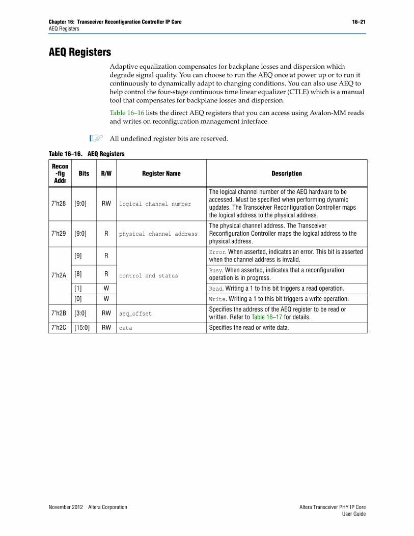
Chapter 16: Transceiver Reconfiguration Controller IP Core 16–21AEQ Registers
AEQ RegistersAdaptive equalization compensates for backplane losses and dispersion which degrade signal quality. You can choose to run the AEQ once at power up or to run it continuously to dynamically adapt to changing conditions. You can also use AEQ to help control the four-stage continuous time linear equalizer (CTLE) which is a manual tool that compensates for backplane losses and dispersion.
Table 16–16 lists the direct AEQ registers that you can access using Avalon-MM reads and writes on reconfiguration management interface.
1 All undefined register bits are reserved.
Table 16–16. AEQ Registers
Recon-fig Addr
Bits R/W Register Name Description
7’h28 [9:0] RW logical channel number
The logical channel number of the AEQ hardware to be accessed. Must be specified when performing dynamic updates. The Transceiver Reconfiguration Controller maps the logical address to the physical address.
7’h29 [9:0] R physical channel addressThe physical channel address. The Transceiver Reconfiguration Controller maps the logical address to the physical address.
7’h2A
[9] R
control and status
Error. When asserted, indicates an error. This bit is asserted when the channel address is invalid.
[8] R Busy. When asserted, indicates that a reconfiguration operation is in progress.
[1] W Read. Writing a 1 to this bit triggers a read operation.
[0] W Write. Writing a 1 to this bit triggers a write operation.
7’h2B [3:0] RW aeq_offsetSpecifies the address of the AEQ register to be read or written. Refer to Table 16–17 for details.
7’h2C [15:0] RW data Specifies the read or write data.
November 2012 Altera Corporation Altera Transceiver PHY IP CoreUser Guide
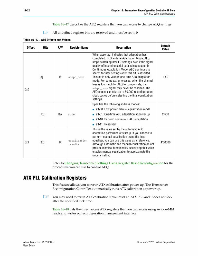
16–22 Chapter 16: Transceiver Reconfiguration Controller IP CoreATX PLL Calibration Registers
Table 16–17 describes the AEQ registers that you can access to change AEQ settings.
1 All undefined register bits are reserved and must be set to 0.
Refer to Changing Transceiver Settings Using Register-Based Reconfiguration for the procedures you can use to control AEQ.
ATX PLL Calibration RegistersThis feature allows you to rerun ATX calibration after power up. The Transceiver Reconfiguration Controller automatically runs ATX calibration at power up.
1 You may need to rerun ATX calibration if you reset an ATX PLL and it does not lock after the specified lock time.
Table 16–18 lists the direct access ATX registers that you can access using Avalon-MM reads and writes on reconfiguration management interface.
Table 16–17. AEQ Offsets and Values
Offset Bits R/W Register Name Description Default Value
0x0
[8] R adapt_done
When asserted, indicates that adaptation has completed. In One-Time Adaptation Mode, AEQ stops searching new EQ settings even if the signal quality of incoming serial data is inadequate. In Continuous Adaptation Mode, AEQ continues to search for new settings after this bit is asserted. This bit is only valid in one-time AEQ adaptation mode. For some extreme cases, when the channel loss is too much for AEQ to compensate, the adapt_done signal may never be asserted. The AEQ engine can take up to 50,000 reconfiguration clock cycles before selecting the final equalization settings.
1b’0
[1:0] RW mode
Specifies the following address modes:
■ 2’b00: Low power manual equalization mode
■ 2’b01: One-time AEQ adaptation at power up
■ 2’b10: Perform continuous AEQ adaptation
■ 2’b11: Reserved
2’b00
0x1 [3:0] R equalization results
This is the value set by the automatic AEQ adaptation performed at startup. If you choose to perform manual equalization using the linear equalizer, you can use this value as a reference. Although automatic and manual equalization do not provide identical functionality, specifying this value enables manual equalization to approximate the original setting.
4’b0000
Altera Transceiver PHY IP Core November 2012 Altera CorporationUser Guide
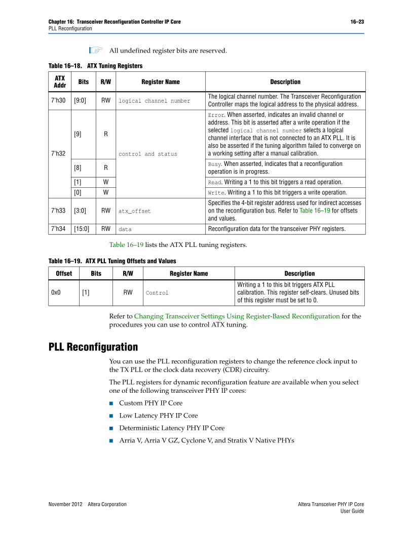
Chapter 16: Transceiver Reconfiguration Controller IP Core 16–23PLL Reconfiguration
1 All undefined register bits are reserved.
Table 16–19 lists the ATX PLL tuning registers.
Refer to Changing Transceiver Settings Using Register-Based Reconfiguration for the procedures you can use to control ATX tuning.
PLL ReconfigurationYou can use the PLL reconfiguration registers to change the reference clock input to the TX PLL or the clock data recovery (CDR) circuitry.
The PLL registers for dynamic reconfiguration feature are available when you select one of the following transceiver PHY IP cores:
■ Custom PHY IP Core
■ Low Latency PHY IP Core
■ Deterministic Latency PHY IP Core
■ Arria V, Arria V GZ, Cyclone V, and Stratix V Native PHYs
Table 16–18. ATX Tuning Registers
ATXAddr Bits R/W Register Name Description
7’h30 [9:0] RW logical channel numberThe logical channel number. The Transceiver Reconfiguration Controller maps the logical address to the physical address.
7’h32
[9] R
control and status
Error. When asserted, indicates an invalid channel or address. This bit is asserted after a write operation if the selected logical channel number selects a logical channel interface that is not connected to an ATX PLL. It is also be asserted if the tuning algorithm failed to converge on a working setting after a manual calibration.
[8] R Busy. When asserted, indicates that a reconfiguration operation is in progress.
[1] W Read. Writing a 1 to this bit triggers a read operation.
[0] W Write. Writing a 1 to this bit triggers a write operation.
7’h33 [3:0] RW atx_offsetSpecifies the 4-bit register address used for indirect accesses on the reconfiguration bus. Refer to Table 16–19 for offsets and values.
7’h34 [15:0] RW data Reconfiguration data for the transceiver PHY registers.
Table 16–19. ATX PLL Tuning Offsets and Values
Offset Bits R/W Register Name Description
0x0 [1] RW ControlWriting a 1 to this bit triggers ATX PLL calibration. This register self-clears. Unused bits of this register must be set to 0.
November 2012 Altera Corporation Altera Transceiver PHY IP CoreUser Guide
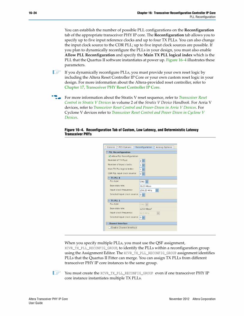
16–24 Chapter 16: Transceiver Reconfiguration Controller IP CorePLL Reconfiguration
You can establish the number of possible PLL configurations on the Reconfiguration tab of the appropriate transceiver PHY IP core. The Reconfiguration tab allows you to specify up to five input reference clocks and up to four TX PLLs. You can also change the input clock source to the CDR PLL; up to five input clock sources are possible. If you plan to dynamically reconfigure the PLLs in your design, you must also enable Allow PLL Reconfiguration and specify the Main TX PLL logical index which is the PLL that the Quartus II software instantiates at power up. Figure 16–4 illustrates these parameters.
1 If you dynamically reconfigure PLLs, you must provide your own reset logic by including the Altera Reset Controller IP Core or your own custom reset logic in your design. For more information about the Altera-provided reset controller, refer to Chapter 17, Transceiver PHY Reset Controller IP Core.
f For more information about the Stratix V reset sequence, refer to Transceiver Reset Control in Stratix V Devices in volume 2 of the Stratix V Device Handbook. For Arria V devices, refer to Transceiver Reset Control and Power-Down in Arria V Devices. For Cyclone V devices refer to Transceiver Reset Control and Power Down in Cyclone V Devices.
When you specify multiple PLLs, you must use the QSF assignment, XCVR_TX_PLL_RECONFIG_GROUP, to identify the PLLs within a reconfiguration group using the Assignment Editor. The XCVR_TX_PLL_RECONFIG_GROUP assignment identifies PLLs that the Quartus II Fitter can merge. You can assign TX PLLs from different transceiver PHY IP core instances to the same group.
1 You must create the XCVR_TX_PLL_RECONFIG_GROUP even if one transceiver PHY IP core instance instantiates multiple TX PLLs.
Figure 16–4. Reconfiguration Tab of Custom, Low Latency, and Deterministic Latency Transceiver PHYs
Altera Transceiver PHY IP Core November 2012 Altera CorporationUser Guide
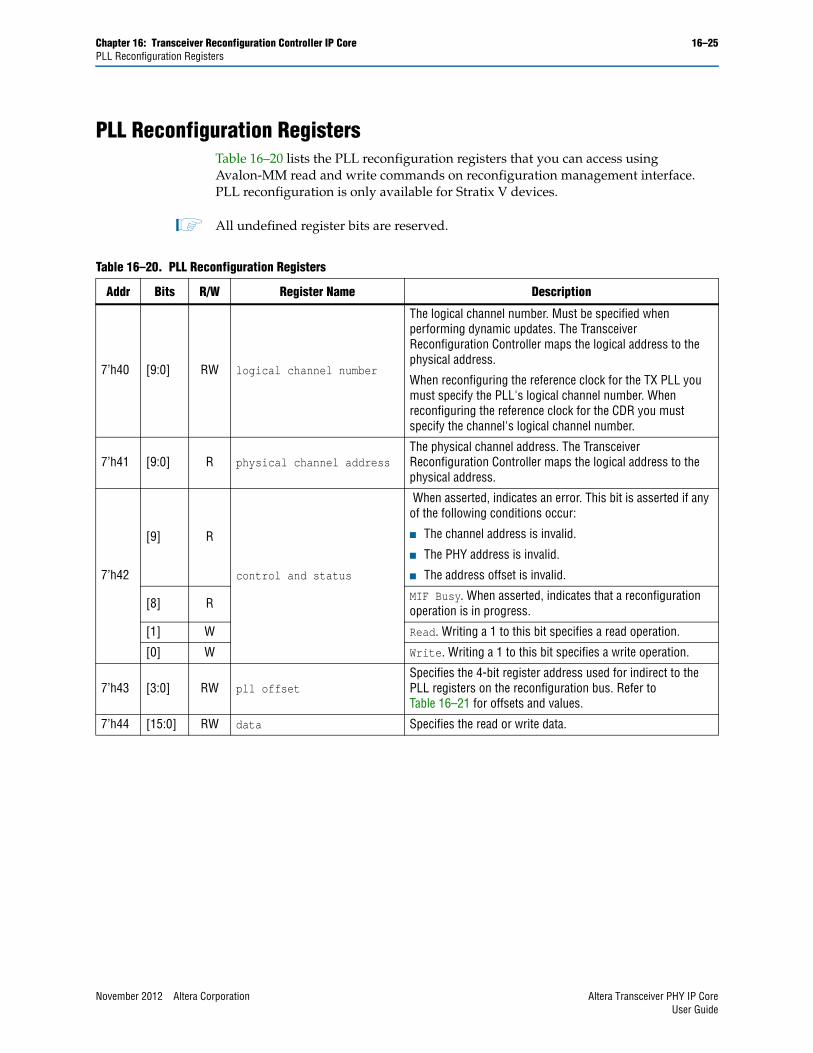
Chapter 16: Transceiver Reconfiguration Controller IP Core 16–25PLL Reconfiguration Registers
PLL Reconfiguration RegistersTable 16–20 lists the PLL reconfiguration registers that you can access using Avalon-MM read and write commands on reconfiguration management interface. PLL reconfiguration is only available for Stratix V devices.
1 All undefined register bits are reserved.
Table 16–20. PLL Reconfiguration Registers
Addr Bits R/W Register Name Description
7’h40 [9:0] RW logical channel number
The logical channel number. Must be specified when performing dynamic updates. The Transceiver Reconfiguration Controller maps the logical address to the physical address.
When reconfiguring the reference clock for the TX PLL you must specify the PLL's logical channel number. When reconfiguring the reference clock for the CDR you must specify the channel's logical channel number.
7’h41 [9:0] R physical channel addressThe physical channel address. The Transceiver Reconfiguration Controller maps the logical address to the physical address.
7’h42
[9] R
control and status
When asserted, indicates an error. This bit is asserted if any of the following conditions occur:
■ The channel address is invalid.
■ The PHY address is invalid.
■ The address offset is invalid.
[8] R MIF Busy. When asserted, indicates that a reconfiguration operation is in progress.
[1] W Read. Writing a 1 to this bit specifies a read operation.
[0] W Write. Writing a 1 to this bit specifies a write operation.
7’h43 [3:0] RW pll offsetSpecifies the 4-bit register address used for indirect to the PLL registers on the reconfiguration bus. Refer to Table 16–21 for offsets and values.
7’h44 [15:0] RW data Specifies the read or write data.
November 2012 Altera Corporation Altera Transceiver PHY IP CoreUser Guide
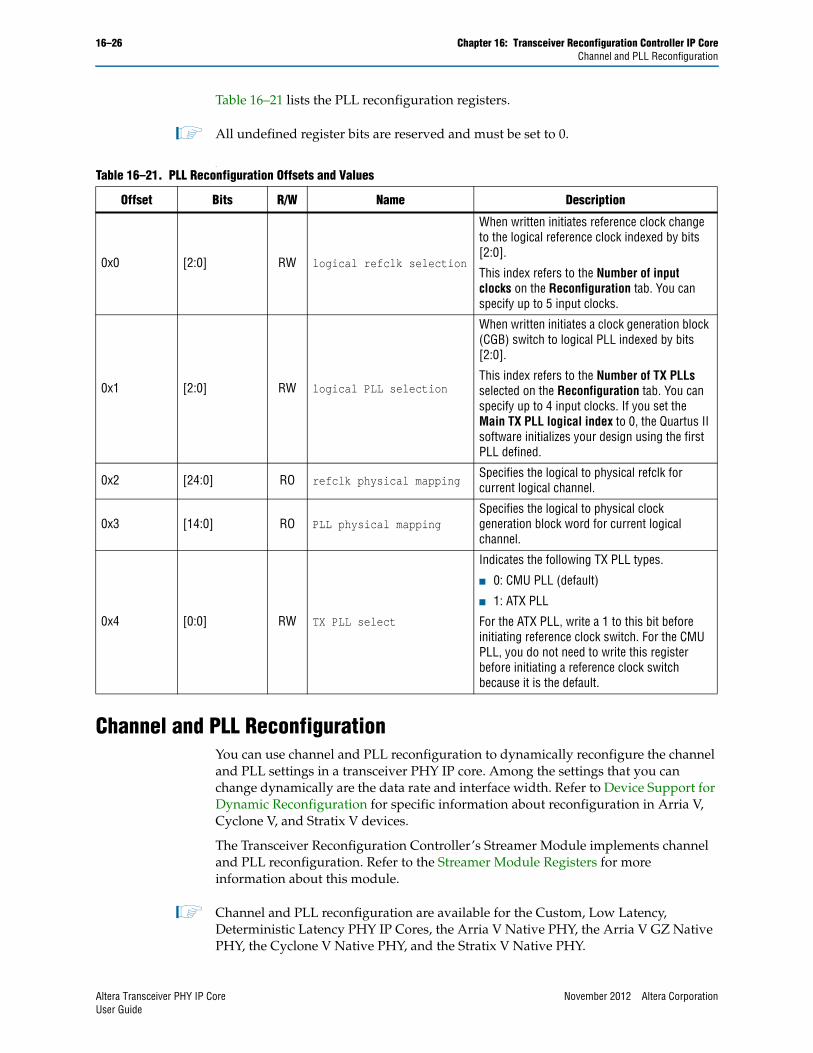
16–26 Chapter 16: Transceiver Reconfiguration Controller IP CoreChannel and PLL Reconfiguration
Table 16–21 lists the PLL reconfiguration registers.
1 All undefined register bits are reserved and must be set to 0.
.
Channel and PLL ReconfigurationYou can use channel and PLL reconfiguration to dynamically reconfigure the channel and PLL settings in a transceiver PHY IP core. Among the settings that you can change dynamically are the data rate and interface width. Refer to Device Support for Dynamic Reconfiguration for specific information about reconfiguration in Arria V, Cyclone V, and Stratix V devices.
The Transceiver Reconfiguration Controller’s Streamer Module implements channel and PLL reconfiguration. Refer to the Streamer Module Registers for more information about this module.
1 Channel and PLL reconfiguration are available for the Custom, Low Latency, Deterministic Latency PHY IP Cores, the Arria V Native PHY, the Arria V GZ Native PHY, the Cyclone V Native PHY, and the Stratix V Native PHY.
Table 16–21. PLL Reconfiguration Offsets and Values
Offset Bits R/W Name Description
0x0 [2:0] RW logical refclk selection
When written initiates reference clock change to the logical reference clock indexed by bits [2:0].
This index refers to the Number of input clocks on the Reconfiguration tab. You can specify up to 5 input clocks.
0x1 [2:0] RW logical PLL selection
When written initiates a clock generation block (CGB) switch to logical PLL indexed by bits [2:0].
This index refers to the Number of TX PLLs selected on the Reconfiguration tab. You can specify up to 4 input clocks. If you set the Main TX PLL logical index to 0, the Quartus II software initializes your design using the first PLL defined.
0x2 [24:0] RO refclk physical mapping Specifies the logical to physical refclk for current logical channel.
0x3 [14:0] RO PLL physical mapping Specifies the logical to physical clock generation block word for current logical channel.
0x4 [0:0] RW TX PLL select
Indicates the following TX PLL types.
■ 0: CMU PLL (default)
■ 1: ATX PLL
For the ATX PLL, write a 1 to this bit before initiating reference clock switch. For the CMU PLL, you do not need to write this register before initiating a reference clock switch because it is the default.
Altera Transceiver PHY IP Core November 2012 Altera CorporationUser Guide
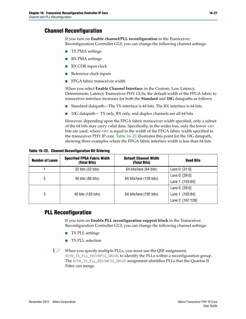
Chapter 16: Transceiver Reconfiguration Controller IP Core 16–27Channel and PLL Reconfiguration
Channel ReconfigurationIf you turn on Enable channel/PLL reconfiguration in the Transceiver Reconfiguration Controller GUI, you can change the following channel settings:
■ TX PMA settings
■ RX PMA settings
■ RX CDR input clock
■ Reference clock inputs
■ FPGA fabric transceiver width
When you select Enable Channel Interface, in the Custom, Low Latency, Deterministic Latency Transceiver PHY GUIs, the default width of the FPGA fabric to transceiver interface increases for both the Standard and 10G datapaths as follows:
■ Standard datapath—The TX interface is 44 bits. The RX interface is 64 bits.
■ 10G datapath— TX only, RX only, and duplex channels are all 64 bits.
However, depending upon the FPGA fabric transceiver width specified, only a subset of the 64 bits may carry valid data. Specifically, in the wider bus, only the lower <n> bits are used, where <n> is equal to the width of the FPGA fabric width specified in the transceiver PHY IP core. Table 16–22 illustrates this point for the 10G datapath, showing three examples where the FPGA fabric interface width is less than 64 bits.
PLL ReconfigurationIf you turn on Enable PLL reconfiguration support block in the Transceiver Reconfiguration Controller GUI, you can change the following channel settings:
■ TX PLL settings
■ TX PLL selection
1 When you specify multiple PLLs, you must use the QSF assignment, XCVR_TX_PLL_RECONFIG_GROUP, to identify the PLLs within a reconfiguration group. The XCVR_TX_PLL_RECONFIG_GROUP assignment identifies PLLs that the Quartus II Fitter can merge.
Table 16–22. Channel Reconfiguration Bit Ordering
Number of Lanes Specified FPGA Fabric Width (Total Bits)
Default Channel Width (Total Bits) Used Bits
1 32 bits (32 bits) 64 bits/lane (64 bits) Lane 0: [31:0]
2 40 bits (80 bits) 64 bits/lane (128 bits)Lane 0: [39:0]
Lane 1: [103:64]
3 40 bits (120 bits) 64 bits/lane (192 bits)
Lane 0: [39:0]
Lane 1: [103:64]
Lane 2: [167:128]
November 2012 Altera Corporation Altera Transceiver PHY IP CoreUser Guide
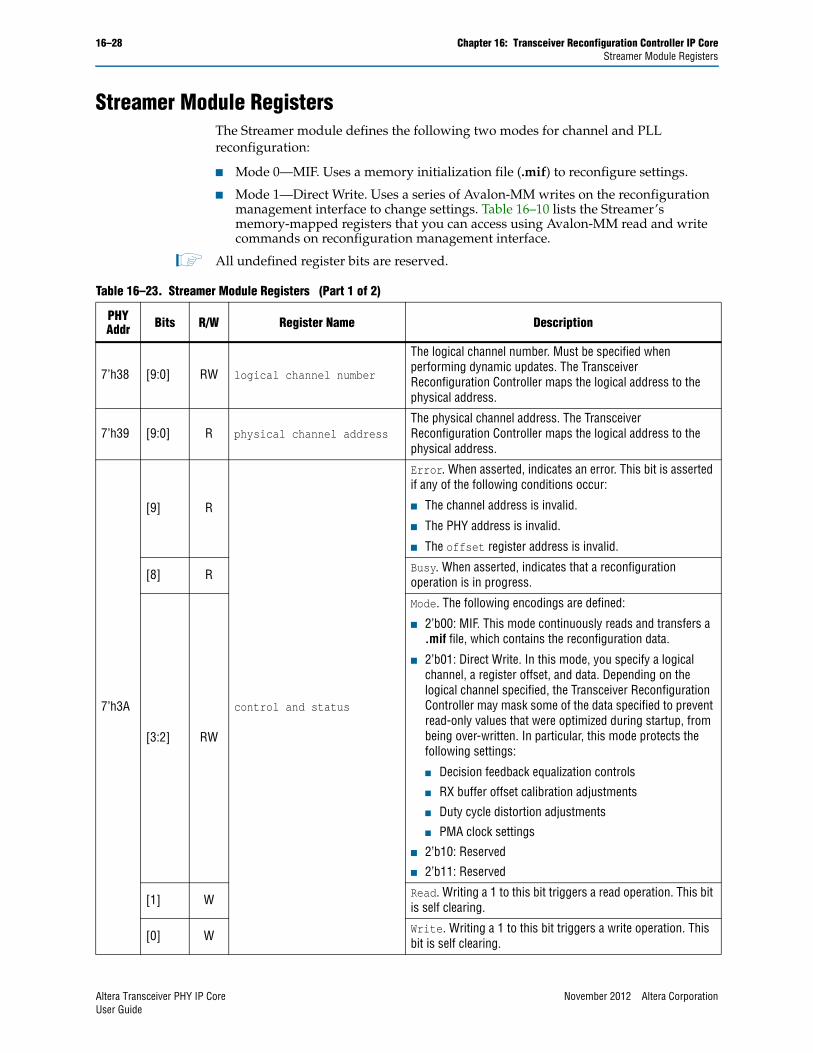
16–28 Chapter 16: Transceiver Reconfiguration Controller IP CoreStreamer Module Registers
Streamer Module RegistersThe Streamer module defines the following two modes for channel and PLL reconfiguration:
■ Mode 0—MIF. Uses a memory initialization file (.mif) to reconfigure settings.
■ Mode 1—Direct Write. Uses a series of Avalon-MM writes on the reconfiguration management interface to change settings. Table 16–10 lists the Streamer’s memory-mapped registers that you can access using Avalon-MM read and write commands on reconfiguration management interface.
1 All undefined register bits are reserved.
Table 16–23. Streamer Module Registers (Part 1 of 2)
PHY Addr Bits R/W Register Name Description
7’h38 [9:0] RW logical channel number
The logical channel number. Must be specified when performing dynamic updates. The Transceiver Reconfiguration Controller maps the logical address to the physical address.
7’h39 [9:0] R physical channel addressThe physical channel address. The Transceiver Reconfiguration Controller maps the logical address to the physical address.
7’h3A
[9] R
control and status
Error. When asserted, indicates an error. This bit is asserted if any of the following conditions occur:
■ The channel address is invalid.
■ The PHY address is invalid.
■ The offset register address is invalid.
[8] R Busy. When asserted, indicates that a reconfiguration operation is in progress.
[3:2] RW
Mode. The following encodings are defined:
■ 2’b00: MIF. This mode continuously reads and transfers a .mif file, which contains the reconfiguration data.
■ 2’b01: Direct Write. In this mode, you specify a logical channel, a register offset, and data. Depending on the logical channel specified, the Transceiver Reconfiguration Controller may mask some of the data specified to prevent read-only values that were optimized during startup, from being over-written. In particular, this mode protects the following settings:
■ Decision feedback equalization controls
■ RX buffer offset calibration adjustments
■ Duty cycle distortion adjustments
■ PMA clock settings
■ 2’b10: Reserved
■ 2’b11: Reserved
[1] W Read. Writing a 1 to this bit triggers a read operation. This bit is self clearing.
[0] W Write. Writing a 1 to this bit triggers a write operation. This bit is self clearing.
Altera Transceiver PHY IP Core November 2012 Altera CorporationUser Guide
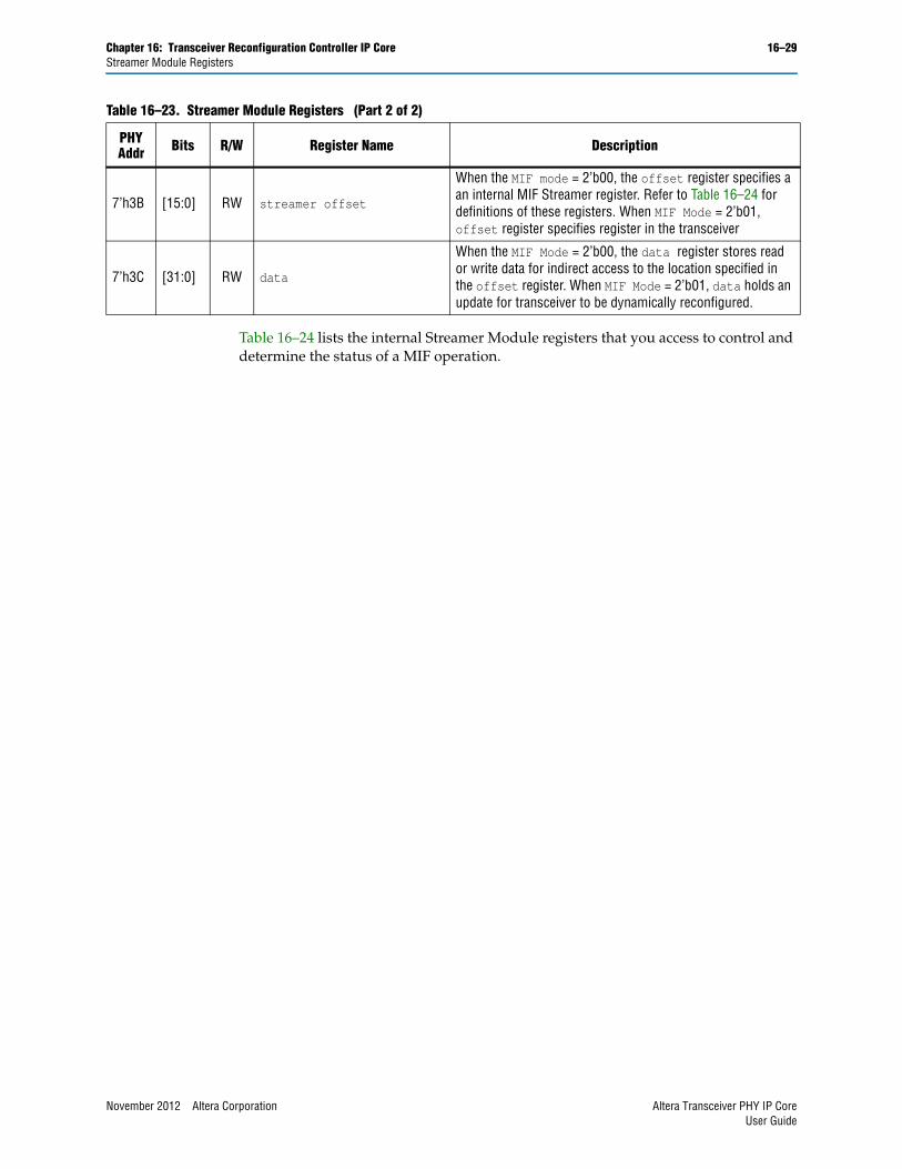
Chapter 16: Transceiver Reconfiguration Controller IP Core 16–29Streamer Module Registers
Table 16–24 lists the internal Streamer Module registers that you access to control and determine the status of a MIF operation.
7’h3B [15:0] RW streamer offset
When the MIF mode = 2’b00, the offset register specifies a an internal MIF Streamer register. Refer to Table 16–24 for definitions of these registers. When MIF Mode = 2’b01, offset register specifies register in the transceiver
7’h3C [31:0] RW data
When the MIF Mode = 2’b00, the data register stores read or write data for indirect access to the location specified in the offset register. When MIF Mode = 2’b01, data holds an update for transceiver to be dynamically reconfigured.
Table 16–23. Streamer Module Registers (Part 2 of 2)
PHY Addr Bits R/W Register Name Description
November 2012 Altera Corporation Altera Transceiver PHY IP CoreUser Guide
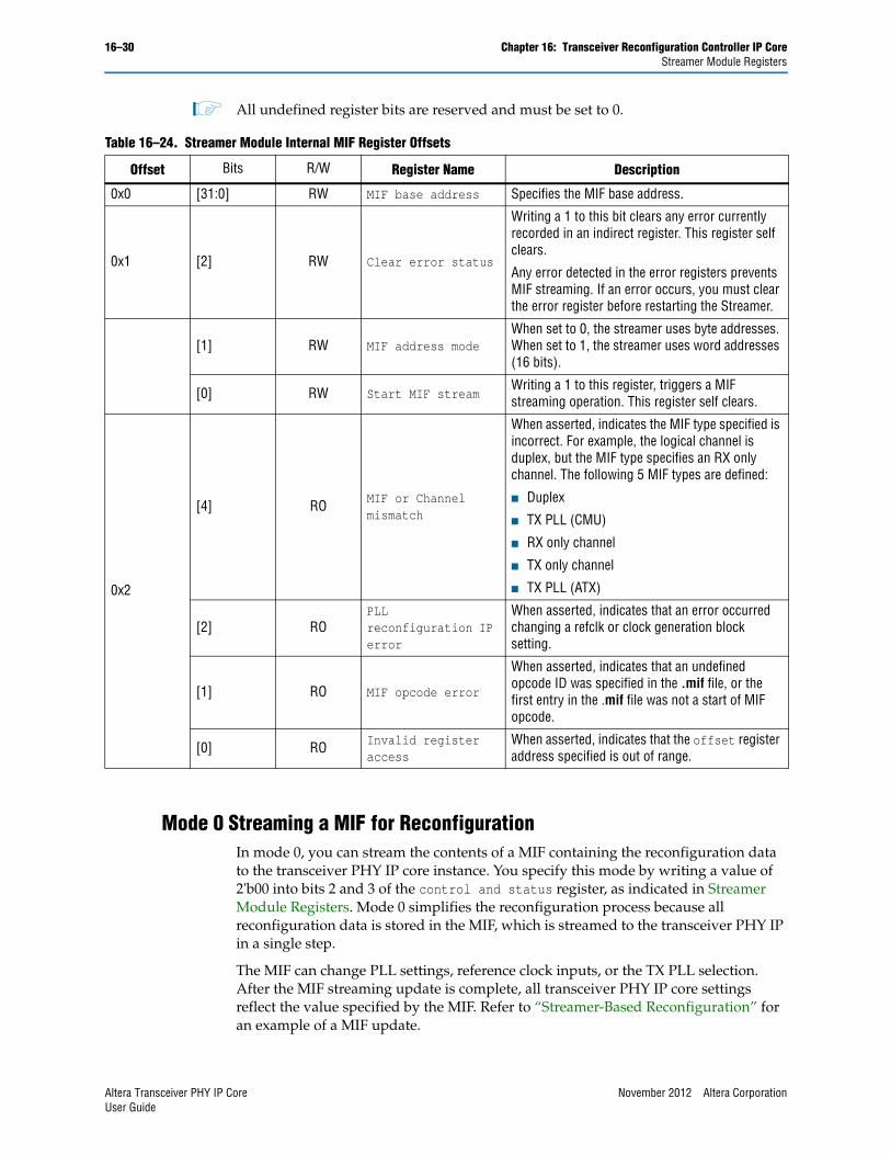
16–30 Chapter 16: Transceiver Reconfiguration Controller IP CoreStreamer Module Registers
1 All undefined register bits are reserved and must be set to 0.
Mode 0 Streaming a MIF for Reconfiguration In mode 0, you can stream the contents of a MIF containing the reconfiguration data to the transceiver PHY IP core instance. You specify this mode by writing a value of 2'b00 into bits 2 and 3 of the control and status register, as indicated in Streamer Module Registers. Mode 0 simplifies the reconfiguration process because all reconfiguration data is stored in the MIF, which is streamed to the transceiver PHY IP in a single step.
The MIF can change PLL settings, reference clock inputs, or the TX PLL selection. After the MIF streaming update is complete, all transceiver PHY IP core settings reflect the value specified by the MIF. Refer to “Streamer-Based Reconfiguration” for an example of a MIF update.
Table 16–24. Streamer Module Internal MIF Register Offsets
Offset Bits R/W Register Name Description
0x0 [31:0] RW MIF base address Specifies the MIF base address.
0x1 [2] RW Clear error status
Writing a 1 to this bit clears any error currently recorded in an indirect register. This register self clears.
Any error detected in the error registers prevents MIF streaming. If an error occurs, you must clear the error register before restarting the Streamer.
[1] RW MIF address modeWhen set to 0, the streamer uses byte addresses. When set to 1, the streamer uses word addresses (16 bits).
[0] RW Start MIF stream Writing a 1 to this register, triggers a MIF streaming operation. This register self clears.
0x2
[4] RO MIF or Channel mismatch
When asserted, indicates the MIF type specified is incorrect. For example, the logical channel is duplex, but the MIF type specifies an RX only channel. The following 5 MIF types are defined:
■ Duplex
■ TX PLL (CMU)
■ RX only channel
■ TX only channel
■ TX PLL (ATX)
[2] ROPLL reconfiguration IP error
When asserted, indicates that an error occurred changing a refclk or clock generation block setting.
[1] RO MIF opcode error
When asserted, indicates that an undefined opcode ID was specified in the .mif file, or the first entry in the .mif file was not a start of MIF opcode.
[0] RO Invalid register access
When asserted, indicates that the offset register address specified is out of range.
Altera Transceiver PHY IP Core November 2012 Altera CorporationUser Guide
Chapter 16: Transceiver Reconfiguration Controller IP Core 16–31MIF Generation
Mode 1 Avalon-MM Direct Writes for Reconfiguration You specify this mode by writing a value of 2'b01 into bits 2 and 3 of the control and status register, as indicated in Table 16–23 on page 16–28. In this mode, you can write directly to transceiver PHY IP core registers to perform reconfiguration. Refer to “Direct Write Reconfiguration” on page 16–39 for an example of an update using mode 1. In mode 1, you can selectively reconfigure portions of the transceiver PHY IP core. Unlike mode 0, mode 1 allows you to write only the data required for a reconfiguration.
MIF GenerationThe Quartus II software automatically generates MIFs after each successful compilation. The MIF stores the configuration data for the transceiver PHY IP cores. MIFs are stored in the reconfig_mif folder of the project's working directly. This folder stores all MIFs associated with the compiled project for each transceiver PHY IP core instance in the design. The parameter settings of PHY IP core instance reflect the currently specified MIF. You can store the MIF in an on-chip ROM or any other type of memory. This memory must connect to the MIF reconfiguration management interface.
Example 16–4 shows file names for the .mif files for a design with two channels. This design example includes two transceiver PHY IP core instances running at different data rates. Both transceiver PHY IP core instances have two TX PLLs specified to support both 1 Gbps and 2.5 Gbps data rates. The Quartus II software generates two TX PLL .mif files for each PLL. The difference between the .mif files is the PLL reference clock specified. To dynamically reconfigure the channel from the initially specified data rate to a new data rate, you can use the MIF streaming function to load the other .mif.
1 When reconfiguration is limited to a few settings, you can create a partial .mif that only includes the settings that must be updated. Refer to Reduced MIF Creation for more information about creating a partial .mif file.
Creating MIFs for Designs that Include Bonded or ATT ChannelsThe Quartus II software automatically generates MIF for all designs that support POF generation with the following exceptions:
■ Designs that use bonded channels so that the same TX PLL output drives several channels
■ ATT channels
■ Non-bonded channels in a design that also includes bonded channels
Example 16–4. Quartus II Generated MIF Files
<project_dir>/reconfig_mif/inst0_1g_channel.mif<project_dir>/reconfig_mif/inst0_1g_txpll0.mif<project_dir>/reconfig_mif/inst0_1g_txpll1.mif<project_dir>/reconfig_mif/inst0_2p5g_channel.mif<project_dir>/reconfig_mif/inst0_2p5g_txpll0.mif<project_dir>/reconfig_mif/inst0_2p5g_txpll1.mif
November 2012 Altera Corporation Altera Transceiver PHY IP CoreUser Guide
16–32 Chapter 16: Transceiver Reconfiguration Controller IP CoreMIF Format
You can generate MIF files for projects that include bonded or ATT channels using the following procedure:
1. Create separate 1-channel designs for each frequency TX PLL frequency that your actual design requires.
2. Compile each design with the Quartus II software.
3. Save the MIF files that Quartus II software generates.
4. Use the MIF files that you have created from your 1-channel designs for reconfiguration in your design that includes bonded clocks.
MIF FormatThe MIF file is organized into records where each record contains the information necessary to carry out the reconfiguration process. There are two types of records: non-data records and data records. A MIF can contain a variable number of records, depending on the target transceiver channel. Both data records and non-data records are 16-bits long.
For both record types the high-order 5 bits represent the length field. A length field of 5’b0, indicates a non-data record which contains an opcode. A length field that is not zero indicates a data record.
For a non-data record, the opcode is represented by the lower 5-bits in the record. Table 16–25 lists the supported opcodes and describes the data content.
For data records, the low-order 11 bits provide a logical offset address. In this case, the length field indicates the number of data records that are written into the specified address. For example, if the length field is set to two, the next two records belong the data record and are written into the offset address.
Table 16–25. Opcodes for MIF Files
Opcode Opcode Description
5’b00000 Reserved
5’b00001 Start of MIF
5’b00010
Channel format indicator specifying the MIF channel type. The following encodings are defined:
■ 3’b000: Duplex channel
■ 3’b001: TX PLL (CMU)
■ 3’b010: RX only channel
■ 3’b011: TX only channel
■ 3’b100: TX PLL (ATX)
5’b00011 Reference Clock switch
5’b00100 CGB switch
5’b00101-5’b11110 Reserved
5’b11111 End of MIF (EOM)
Altera Transceiver PHY IP Core November 2012 Altera CorporationUser Guide
Chapter 16: Transceiver Reconfiguration Controller IP Core 16–33xcvr_diffmifgen Utility
All MIF files must contain the lines shown in Table 16–26.
Figure 16–5 provides an example of a typical MIF format. Entries 3, 7, and <n> are data records.
xcvr_diffmifgen UtilityThe xcvr_diffmifgen utility allows you to create a .mif file that includes the differences in settings between two configurations. For example, if you have two configurations, inst0_1g_txpll0.mif that sets a TX PLL0 bandwidth to 1 Gbps and inst0_5g_txpll0.mif that sets the TX PLL0 bandwidth to 5 Gbps, the xcvr_diffmifgen utility creates to_inst0_1g_txpll0.mif and to_inst0_5g_txpll0.mif that include the information necessary to change from 1 Gbps to 5 Gbps and from 5 Gbps to 1 Gbps. You can use these files to reduce reconfiguration and simulation times.
The xcvr_diffmifgen utility can operate on up to five MIF files. This utility only works on MIF files at the same revision level. If you try to compare MIF files that are not at the same revision level, xcvr_diffmifgen issues a warning.
1 You can also use the Reduced MIF Creation to create reduced MIF files.
Table 16–26. Required Lines for All MIFs
Line Number Description Content Includes
0 Specifies start of the reconfiguration MIF Start of MIF opcode
1 Specifies the type of MIF Type of MIF opcode
2 Specifies the reference clock RefClk switch opcode
3 Specifies the PLL switch CGB PLL switch opcode
Last Specifies end of reconfiguration MIF End of MIF Opcode
Figure 16–5. MIF File Format
Length = 00
1
2
3
4
5
6
7
8
<n>
<n>+1
<n>+2
<n>+3
MIF/Quartus Version Opcode = Start of MIF
Length = 0 Input Clock Index Opcode = Input Clock Index
Length = 0 PLL Index Opcode = PLL
Length = 0 Reserved Opcode = End of MIF
Length = 3 Offset Address N
Data for Offset N
Length = 1 Offset M
Data for Offset M
Data for Offset N + 1
Data for Offset N + 2
Length = 2 Offset Address L
Data for Offset L
Data for Offset L + 1
15 11 10
......
5 04
November 2012 Altera Corporation Altera Transceiver PHY IP CoreUser Guide
16–34 Chapter 16: Transceiver Reconfiguration Controller IP Corexcvr_diffmifgen Utility
Example 16–5 shows the command usage.
The format of the reduced MIF file is the same as for the original MIF files as described in MIF Format. The reduced MIF file, preserves the lines shown in Table 16–26.
For each difference between the files compared, the reduced MIF file includes the following two records:
1. A record indicating the length and address of the change.
2. The changed data.
Example 16–5. xcvr_diffmifgen
xcvr_diffmifgen <options> <MIF file 1> <MIF file 2> <Mif file n>
Arguments:-h: Displays help-noopt: The output file is not optimized
Table 16–27. Required Lines for All MIFs
Line Number Description Content Includes
0 Specifies start of the reconfiguration MIF Start of MIF opcode
1 Specifies the type of MIF Type of MIF opcode
2 Specifies the reference clock RefClk switch opcode
3 Specifies the PLL switch CGB PLL switch opcode
Last Specifies end of reconfiguration MIF End of MIF Opcode
Altera Transceiver PHY IP Core November 2012 Altera CorporationUser Guide
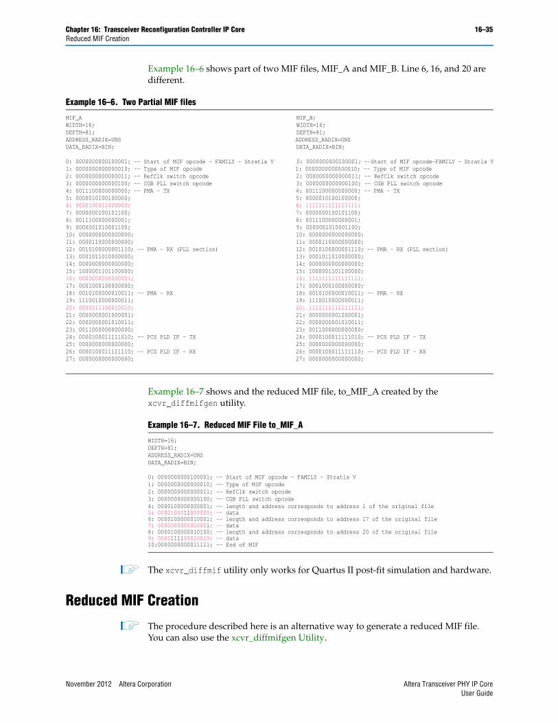
Chapter 16: Transceiver Reconfiguration Controller IP Core 16–35Reduced MIF Creation
Example 16–6 shows part of two MIF files, MIF_A and MIF_B. Line 6, 16, and 20 are different.
Example 16–7 shows and the reduced MIF file, to_MIF_A created by the xcvr_diffmifgen utility.
1 The xcvr_diffmif utility only works for Quartus II post-fit simulation and hardware.
Reduced MIF Creation
1 The procedure described here is an alternative way to generate a reduced MIF file. You can also use the xcvr_diffmifgen Utility.
Example 16–6. Two Partial MIF files
MIF_A MIF_B;WIDTH=16; WIDTH=16;DEPTH=81; DEPTH=81;ADDRESS_RADIX=UNS ADDRESS_RADIX=UNSDATA_RADIX=BIN; DATA_RADIX=BIN;
0: 0000000000100001; -- Start of MIF opcode - FAMILY - Stratix V 0: 0000000000100001; --Start of MIF opcode-FAMILY - Stratix V1: 0000000000000010; -- Type of MIF opcode 1: 0000000000000010; -- Type of MIF opcode2: 0000000000000011; -- RefClk switch opcode 2: 0000000000000011; -- RefClk switch opcode3: 0000000000000100; -- CGB PLL switch opcode 3: 0000000000000100; -- CGB PLL switch opcode4: 0011100000000000; -- PMA - TX 4: 0011100000000000; -- PMA - TX5: 0000010100100000; 5: 0000010100100000;6: 0000100011000000; 6: 1111111111111111;7: 0000000100101100; 7: 0000000100101100;8: 0011100000000001; 8: 0011100000000001;9: 0000001010001100; 9: 0000001010001100;10: 0000000000000000; 10: 0000000000000000;11: 0000110000000000; 11: 0000110000000000;12: 0010100000001110; -- PMA - RX (PLL section) 12: 0010100000001110; -- PMA - RX (PLL section)13: 0001011010000000; 13: 0001011010000000;14: 0000000000000000; 14: 0000000000000000;15: 1000001101100000; 15: 1000001101100000;16: 0000000000000001; 16: 1111111111111111;17: 0001000100000000; 17: 0001000100000000;18: 0010100000010011; -- PMA - RX 18: 0010100000010011; -- PMA - RX19: 1110010000000011; 19: 1110010000000011;20: 0000111100010010; 20: 1111111111111111;21: 0000000001000001; 21: 0000000001000001;22: 0000000001010011; 22: 0000000001010011;23: 0011000000000000; 23: 0011000000000000;24: 0000100011111010; -- PCS PLD IF - TX 24: 0000100011111010; -- PCS PLD IF - TX25: 0000000000000000; 25: 0000000000000000;26: 0000100011111110; -- PCS PLD IF - RX 26: 0000100011111110; -- PCS PLD IF - RX27: 0000000000000000; 27: 0000000000000000;
Example 16–7. Reduced MIF File to_MIF_A
WIDTH=16;DEPTH=81;ADDRESS_RADIX=UNSDATA_RADIX=BIN;
0: 0000000000100001; -- Start of MIF opcode - FAMILY - Stratix V1: 0000000000000010; -- Type of MIF opcode2: 0000000000000011; -- RefClk switch opcode3: 0000000000000100; -- CGB PLL switch opcode4: 0000100000000001; -- length and address corresponds to address 1 of the original file5: 0000100011000000; -- data 6: 0000100000010001; -- length and address corresponds to address 17 of the original file7: 0000000000000001; -- data8: 0000100000010100; -- length and address corresponds to address 20 of the original file9: 0000111100010010; -- data10:0000000000011111; -- End of MIF
November 2012 Altera Corporation Altera Transceiver PHY IP CoreUser Guide
16–36 Chapter 16: Transceiver Reconfiguration Controller IP CoreChanging Transceiver Settings Using Register-Based Reconfiguration
You can create a reduced MIF from the following two MIFs:
■ Original MIF—contains the transceiver settings that were specified during the initial compilation
■ Reconfigured MIF—contains the new transceiver settings. You generate the reconfigured MIF by modifying the original transceiver settings. For example, if the original compilation specifies a clock divider value of 1 and the reconfigured compilation specifies a clock divider value of 2, the MIF files reflect that change. The reduced MIF contains only the changed content. In this example, the difference between the two MIFs would be the clock divider value.
Follow these steps to generate a reduced MIF:
1. Determine the content differences between the original MIF and the reconfigured MIF. For this example, assume there are bit differences at offset 5 and offset 20. These offsets reside in the PMA-TX and PMA-RX sections of the MIF.
2. Use a text editor to create a new reduced MIF file. In this example, we will call the reduced MIF reduced_mif.mif. Copy the WIDTH, DEPTH, ADDRESS_RADIX, DATA_RADIX and CONTENT BEGIN lines from the original MIF to reduced_mif.mif.
3. Copy offsets 0-3 as described Table 16–26 from the original MIF to reduced_mif.mif. The reconfiguration MIF must always include these lines.
4. Copy all offsets of the PMA-TX and PMA-RX sections from the reconfigured MIF to reduced_mif.mif.
5. Copy the End of MIF opcode offset and END; from the original MIF to reduced_mif.mif.
6. Renumber reduced_mif.mif sequentially and update the DEPTH variable with the new value. The new value equals the number offsets in reduced_mif.mif.
You can now use reduced_mif.mif to reconfigure the transceiver.
Changing Transceiver Settings Using Register-Based ReconfigurationIn register-based mode, you use a sequence of Avalon-MM writes and reads to update individual transceiver settings. The following section describes how to perform a register-based reconfiguration read and write.
Register-Based WriteComplete the following steps to perform a register-based write:
1. Read the control and status register busy bit (bit 8) until it is clear.
2. Write the logical channel number of the channel to be updated to the logical channel number register.
3. Write the <feature> offset address.
4. Write the appropriate data value to the data register.
5. Write the control and status register write bit to 1’b1.
6. Read the control and status register busy bit. Continue to read the busy bit while its value is one.
Altera Transceiver PHY IP Core November 2012 Altera CorporationUser Guide
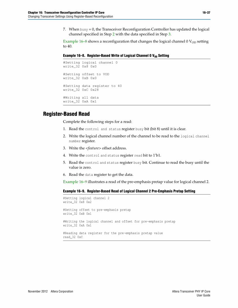
Chapter 16: Transceiver Reconfiguration Controller IP Core 16–37Changing Transceiver Settings Using Register-Based Reconfiguration
7. When busy = 0, the Transceiver Reconfiguration Controller has updated the logical channel specified in Step 2 with the data specified in Step 3.
Example 16–8 shows a reconfiguration that changes the logical channel 0 VOD setting to 40.
Register-Based ReadComplete the following steps for a read:
1. Read the control and status register busy bit (bit 8) until it is clear.
2. Write the logical channel number of the channel to be read to the logical channel number register.
3. Write the <feature> offset address.
4. Write the control and status register read bit to 1’b1.
5. Read the control and status register busy bit. Continue to read the busy until the value is zero.
6. Read the data register to get the data.
Example 16–9 illustrates a read of the pre-emphasis pretap value for logical channel 2.
Example 16–8. Register-Based Write of Logical Channel 0 VOD Setting
#Setting logical channel 0write_32 0x8 0x0
#Setting offset to VODwrite_32 0xB 0x0
#Setting data register to 40write_32 0xC 0x28
#Writing all datawrite_32 0xA 0x1
Example 16–9. Register-Based Read of Logical Channel 2 Pre-Emphasis Pretap Setting
#Setting logical channel 2write_32 0x8 0x2
#Setting offset to pre-emphasis pretapwrite_32 0xB 0x1
#Writing the logical channel and offset for pre-emphasis pretapwrite_32 0xA 0x1
#Reading data register for the pre-emphasis pretap valueread_32 0xC
November 2012 Altera Corporation Altera Transceiver PHY IP CoreUser Guide
16–38 Chapter 16: Transceiver Reconfiguration Controller IP CoreChanging Transceiver Settings Using Streamer-Based Reconfiguration
Changing Transceiver Settings Using Streamer-Based ReconfigurationThe Streamer’s registers allow you to change to the PCS datapath settings, clock settings, and PLL parameters by reading the new settings from an on- or off-chip ROM. Streamer Module Registers lists the Streamer’s memory-mapped registers that you can access using Avalon-MM read and write commands on reconfiguration management interface.
The following sections show how to change transceiver settings using Streamer modes 0 and 1.
Streamer-Based ReconfigurationFollow these steps to reconfigure a transceiver setting by streaming the contents of a MIF file through the Streamer Module.
1. Write the logical channel number to the Streamer logical channel register.
2. Write MIF mode, 2’b00, to the Streamer control and status register mode bits.
3. Write the MIF base address, 0x0, to the Streamer offset register.
4. Write the base address of the MIF file to the Streamer data register.
5. Write the Streamer control and status register write bit to 1'b1 to initiate a write of all the data set in the previous steps.
6. Write to the Streamer offset register with the value to start a MIF stream, 0x1.
7. Write the Streamer internal data register with the value 0x3 to setup the streaming of the MIF.
8. Write to the Streamer control and status register to 1'b1, to initiate the streaming operation.
9. Read the control and status register busy bit. When the busy bit is deasserted, the MIF streaming operation has completed.
Altera Transceiver PHY IP Core November 2012 Altera CorporationUser Guide
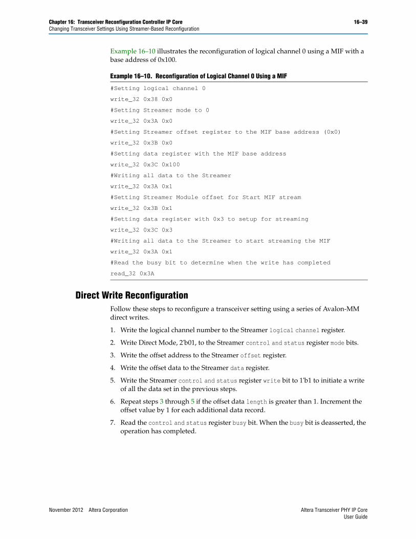
Chapter 16: Transceiver Reconfiguration Controller IP Core 16–39Changing Transceiver Settings Using Streamer-Based Reconfiguration
Example 16–10 illustrates the reconfiguration of logical channel 0 using a MIF with a base address of 0x100.
Direct Write ReconfigurationFollow these steps to reconfigure a transceiver setting using a series of Avalon-MM direct writes.
1. Write the logical channel number to the Streamer logical channel register.
2. Write Direct Mode, 2'b01, to the Streamer control and status register mode bits.
3. Write the offset address to the Streamer offset register.
4. Write the offset data to the Streamer data register.
5. Write the Streamer control and status register write bit to 1'b1 to initiate a write of all the data set in the previous steps.
6. Repeat steps 3 through 5 if the offset data length is greater than 1. Increment the offset value by 1 for each additional data record.
7. Read the control and status register busy bit. When the busy bit is deasserted, the operation has completed.
Example 16–10. Reconfiguration of Logical Channel 0 Using a MIF
#Setting logical channel 0
write_32 0x38 0x0
#Setting Streamer mode to 0
write_32 0x3A 0x0
#Setting Streamer offset register to the MIF base address (0x0)
write_32 0x3B 0x0
#Setting data register with the MIF base address
write_32 0x3C 0x100
#Writing all data to the Streamer
write_32 0x3A 0x1
#Setting Streamer Module offset for Start MIF stream
write_32 0x3B 0x1
#Setting data register with 0x3 to setup for streaming
write_32 0x3C 0x3
#Writing all data to the Streamer to start streaming the MIF
write_32 0x3A 0x1
#Read the busy bit to determine when the write has completed
read_32 0x3A
November 2012 Altera Corporation Altera Transceiver PHY IP CoreUser Guide
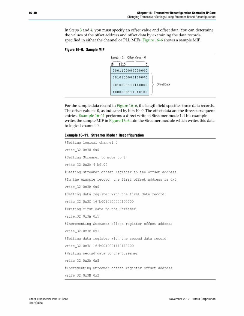
16–40 Chapter 16: Transceiver Reconfiguration Controller IP CoreChanging Transceiver Settings Using Streamer-Based Reconfiguration
In Steps 3 and 4, you must specify an offset value and offset data. You can determine the values of the offset address and offset data by examining the data records specified in either the channel or PLL MIFs. Figure 16–6 shows a sample MIF.
For the sample data record in Figure 16–6, the length field specifies three data records. The offset value is 0, as indicated by bits 10–0. The offset data are the three subsequent entries. Example 16–11 performs a direct write in Streamer mode 1. This example writes the sample MIF in Figure 16–6 into the Streamer module which writes this data to logical channel 0.
Figure 16–6. Sample MIF
Example 16–11. Streamer Mode 1 Reconfiguration
#Setting logical channel 0
write_32 0x38 0x0
#Setting Streamer to mode to 1
write_32 0x3A 4'b0100
#Setting Streamer offset register to the offset address
#In the example record, the first offset address is 0x0
write_32 0x3B 0x0
#Setting data register with the first data record
write_32 0x3C 16'b0010100000100000
#Writing first data to the Streamer
write_32 0x3A 0x5
#Incrementing Streamer offset register offset address
write_32 0x3B 0x1
#Setting data register with the second data record
write_32 0x3C 16'b0010001110110000
#Writing second data to the Streamer
write_32 0x3A 0x5
#Incrementing Streamer offset register offset address
write_32 0x3B 0x2
0 0 0 1 1 0 0 0 0 0 0 0 0 0 0 0
0 0 1 0 1 0 0 0 0 0 1 0 0 0 0 0
0 0 1 0 0 0 1 1 1 0 1 1 0 0 0 0
1 0 0 0 0 0 0 1 1 1 0 1 0 1 0 0
Length = 3 Offset Value = 0
Offset Data
15 1110 0
Altera Transceiver PHY IP Core November 2012 Altera CorporationUser Guide
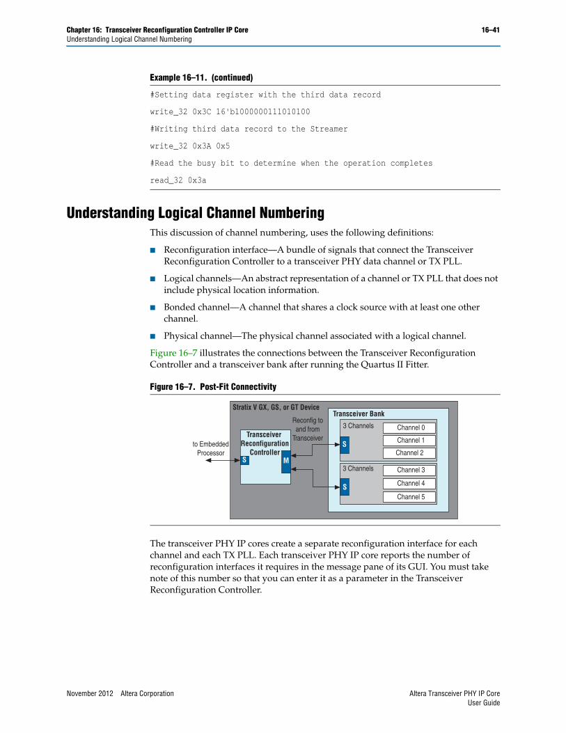
Chapter 16: Transceiver Reconfiguration Controller IP Core 16–41Understanding Logical Channel Numbering
Understanding Logical Channel NumberingThis discussion of channel numbering, uses the following definitions:
■ Reconfiguration interface—A bundle of signals that connect the Transceiver Reconfiguration Controller to a transceiver PHY data channel or TX PLL.
■ Logical channels—An abstract representation of a channel or TX PLL that does not include physical location information.
■ Bonded channel—A channel that shares a clock source with at least one other channel.
■ Physical channel—The physical channel associated with a logical channel.
Figure 16–7 illustrates the connections between the Transceiver Reconfiguration Controller and a transceiver bank after running the Quartus II Fitter.
The transceiver PHY IP cores create a separate reconfiguration interface for each channel and each TX PLL. Each transceiver PHY IP core reports the number of reconfiguration interfaces it requires in the message pane of its GUI. You must take note of this number so that you can enter it as a parameter in the Transceiver Reconfiguration Controller.
Example 16–11. (continued)
#Setting data register with the third data record
write_32 0x3C 16'b1000000111010100
#Writing third data record to the Streamer
write_32 0x3A 0x5
#Read the busy bit to determine when the operation completes
read_32 0x3a
Figure 16–7. Post-Fit Connectivity
Transceiver Reconfiguration
Controller
Transceiver Bank
3 Channels
3 Channels
Channel 2
Channel 1
Channel 0
Channel 3
Channel 5
Channel 4
S M
to EmbeddedProcessor
Reconfig to and from
Transceiver
Stratix V GX, GS, or GT Device
S
S
November 2012 Altera Corporation Altera Transceiver PHY IP CoreUser Guide
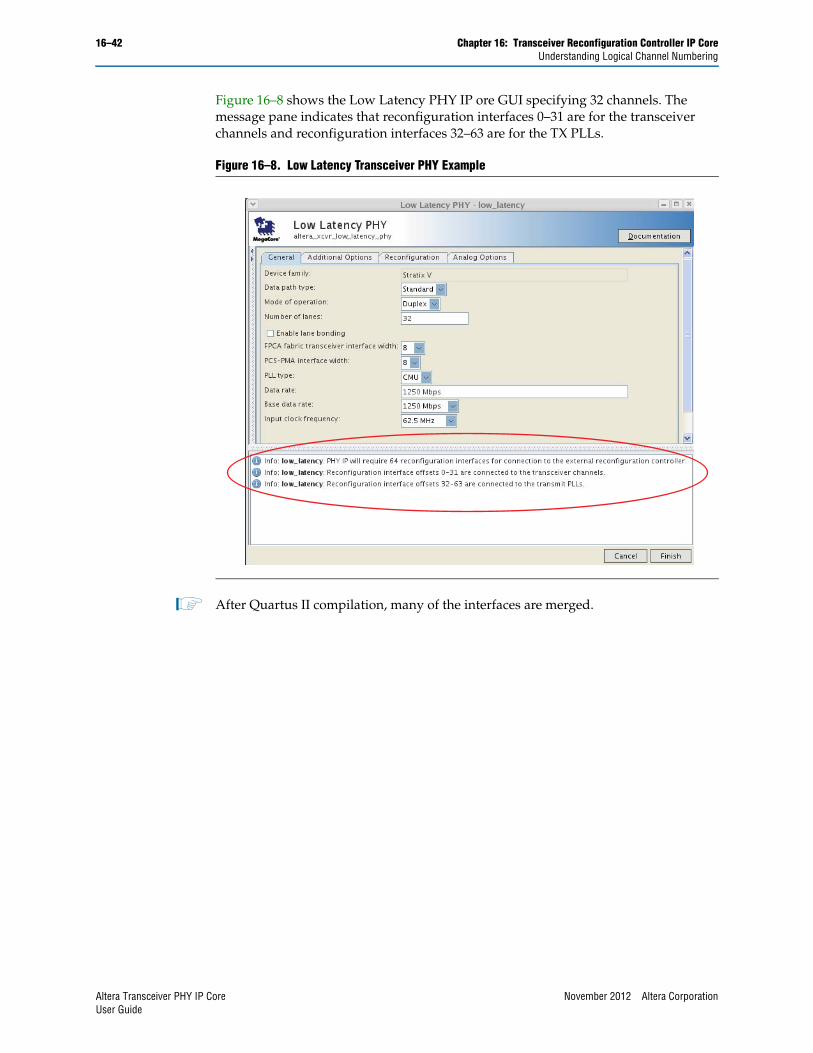
16–42 Chapter 16: Transceiver Reconfiguration Controller IP CoreUnderstanding Logical Channel Numbering
Figure 16–8 shows the Low Latency PHY IP ore GUI specifying 32 channels. The message pane indicates that reconfiguration interfaces 0–31 are for the transceiver channels and reconfiguration interfaces 32–63 are for the TX PLLs.
1 After Quartus II compilation, many of the interfaces are merged.
Figure 16–8. Low Latency Transceiver PHY Example
Altera Transceiver PHY IP Core November 2012 Altera CorporationUser Guide
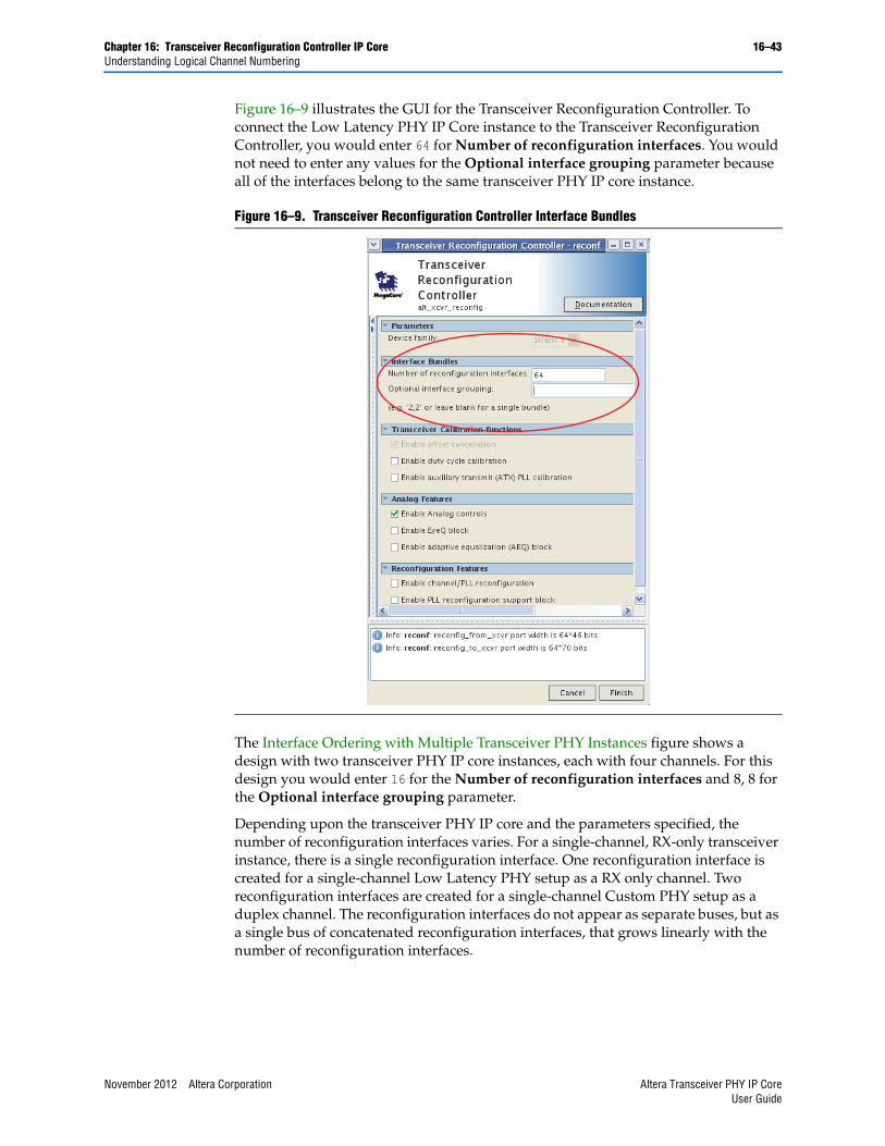
Chapter 16: Transceiver Reconfiguration Controller IP Core 16–43Understanding Logical Channel Numbering
Figure 16–9 illustrates the GUI for the Transceiver Reconfiguration Controller. To connect the Low Latency PHY IP Core instance to the Transceiver Reconfiguration Controller, you would enter 64 for Number of reconfiguration interfaces. You would not need to enter any values for the Optional interface grouping parameter because all of the interfaces belong to the same transceiver PHY IP core instance.
The Interface Ordering with Multiple Transceiver PHY Instances figure shows a design with two transceiver PHY IP core instances, each with four channels. For this design you would enter 16 for the Number of reconfiguration interfaces and 8, 8 for the Optional interface grouping parameter.
Depending upon the transceiver PHY IP core and the parameters specified, the number of reconfiguration interfaces varies. For a single-channel, RX-only transceiver instance, there is a single reconfiguration interface. One reconfiguration interface is created for a single-channel Low Latency PHY setup as a RX only channel. Two reconfiguration interfaces are created for a single-channel Custom PHY setup as a duplex channel. The reconfiguration interfaces do not appear as separate buses, but as a single bus of concatenated reconfiguration interfaces, that grows linearly with the number of reconfiguration interfaces.
Figure 16–9. Transceiver Reconfiguration Controller Interface Bundles
November 2012 Altera Corporation Altera Transceiver PHY IP CoreUser Guide
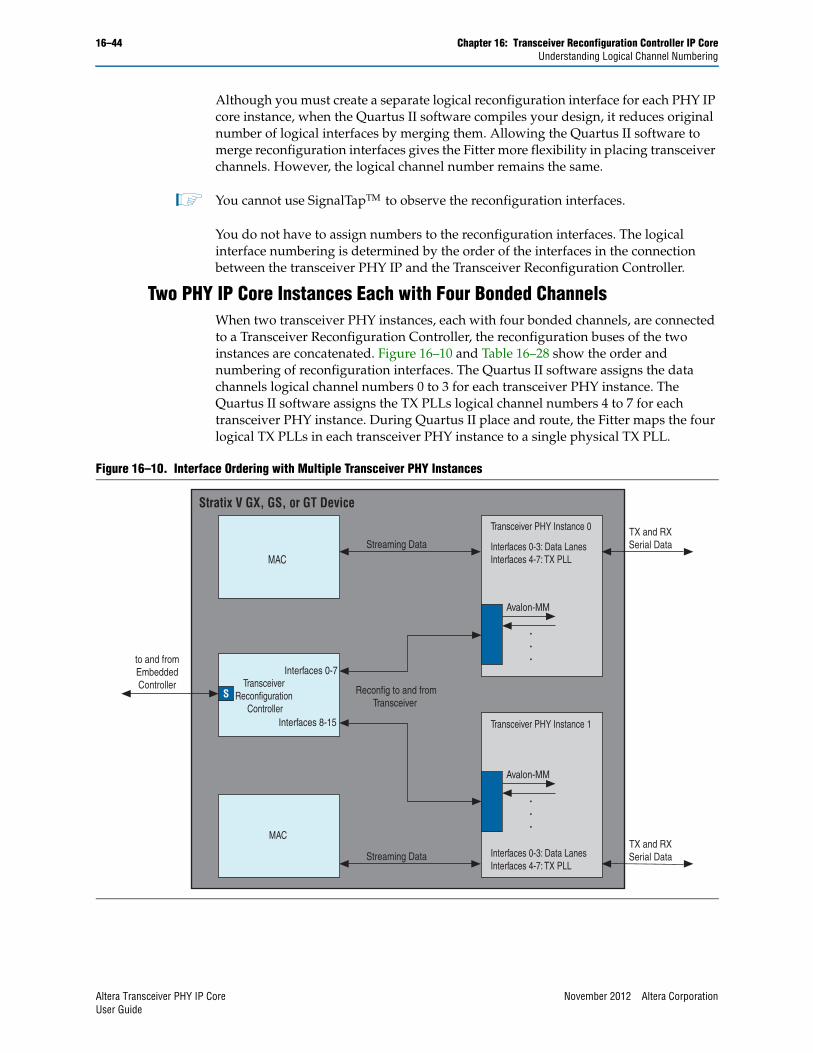
16–44 Chapter 16: Transceiver Reconfiguration Controller IP CoreUnderstanding Logical Channel Numbering
Although you must create a separate logical reconfiguration interface for each PHY IP core instance, when the Quartus II software compiles your design, it reduces original number of logical interfaces by merging them. Allowing the Quartus II software to merge reconfiguration interfaces gives the Fitter more flexibility in placing transceiver channels. However, the logical channel number remains the same.
1 You cannot use SignalTapTM to observe the reconfiguration interfaces.
You do not have to assign numbers to the reconfiguration interfaces. The logical interface numbering is determined by the order of the interfaces in the connection between the transceiver PHY IP and the Transceiver Reconfiguration Controller.
Two PHY IP Core Instances Each with Four Bonded ChannelsWhen two transceiver PHY instances, each with four bonded channels, are connected to a Transceiver Reconfiguration Controller, the reconfiguration buses of the two instances are concatenated. Figure 16–10 and Table 16–28 show the order and numbering of reconfiguration interfaces. The Quartus II software assigns the data channels logical channel numbers 0 to 3 for each transceiver PHY instance. The Quartus II software assigns the TX PLLs logical channel numbers 4 to 7 for each transceiver PHY instance. During Quartus II place and route, the Fitter maps the four logical TX PLLs in each transceiver PHY instance to a single physical TX PLL.
Figure 16–10. Interface Ordering with Multiple Transceiver PHY Instances
to and fromEmbeddedController Transceiver
Reconfiguration Controller
S
Interfaces 0-7
Interfaces 8-15
Reconfig to and fromTransceiver
Transceiver PHY Instance 1
Avalon-MM
Streaming Data
Streaming Data
Transceiver PHY Instance 0
Avalon-MM
Interfaces 0-3: Data LanesInterfaces 4-7: TX PLL
Interfaces 0-3: Data LanesInterfaces 4-7: TX PLL
TX and RXSerial Data
TX and RXSerial Data
MAC
MAC
Stratix V GX, GS, or GT Device
.
.
.
.
.
.
Altera Transceiver PHY IP Core November 2012 Altera CorporationUser Guide
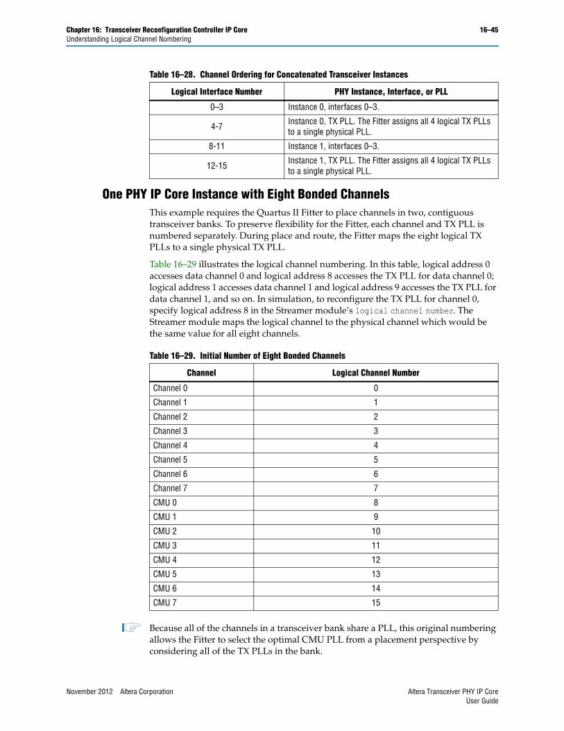
Chapter 16: Transceiver Reconfiguration Controller IP Core 16–45Understanding Logical Channel Numbering
One PHY IP Core Instance with Eight Bonded ChannelsThis example requires the Quartus II Fitter to place channels in two, contiguous transceiver banks. To preserve flexibility for the Fitter, each channel and TX PLL is numbered separately. During place and route, the Fitter maps the eight logical TX PLLs to a single physical TX PLL.
Table 16–29 illustrates the logical channel numbering. In this table, logical address 0 accesses data channel 0 and logical address 8 accesses the TX PLL for data channel 0; logical address 1 accesses data channel 1 and logical address 9 accesses the TX PLL for data channel 1, and so on. In simulation, to reconfigure the TX PLL for channel 0, specify logical address 8 in the Streamer module’s logical channel number. The Streamer module maps the logical channel to the physical channel which would be the same value for all eight channels.
1 Because all of the channels in a transceiver bank share a PLL, this original numbering allows the Fitter to select the optimal CMU PLL from a placement perspective by considering all of the TX PLLs in the bank.
Table 16–28. Channel Ordering for Concatenated Transceiver Instances
Logical Interface Number PHY Instance, Interface, or PLL
0–3 Instance 0, interfaces 0–3.
4-7 Instance 0, TX PLL. The Fitter assigns all 4 logical TX PLLs to a single physical PLL.
8-11 Instance 1, interfaces 0–3.
12-15 Instance 1, TX PLL. The Fitter assigns all 4 logical TX PLLs to a single physical PLL.
Table 16–29. Initial Number of Eight Bonded Channels
Channel Logical Channel Number
Channel 0 0
Channel 1 1
Channel 2 2
Channel 3 3
Channel 4 4
Channel 5 5
Channel 6 6
Channel 7 7
CMU 0 8
CMU 1 9
CMU 2 10
CMU 3 11
CMU 4 12
CMU 5 13
CMU 6 14
CMU 7 15
November 2012 Altera Corporation Altera Transceiver PHY IP CoreUser Guide
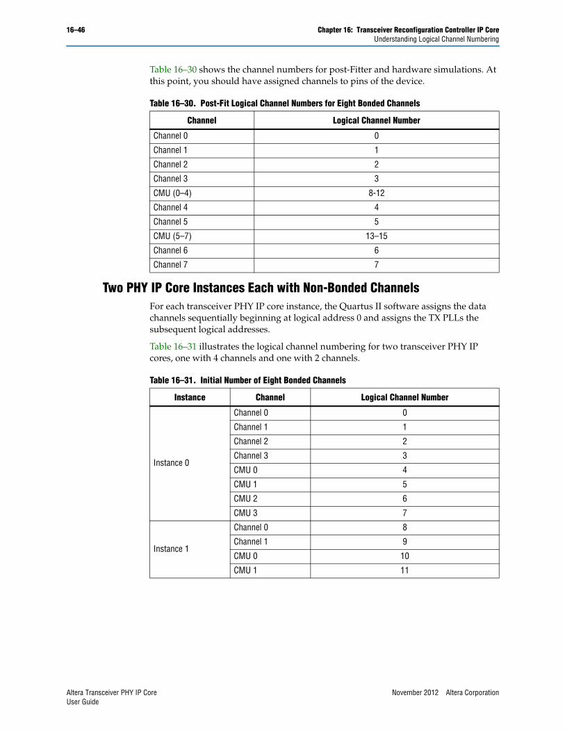
16–46 Chapter 16: Transceiver Reconfiguration Controller IP CoreUnderstanding Logical Channel Numbering
Table 16–30 shows the channel numbers for post-Fitter and hardware simulations. At this point, you should have assigned channels to pins of the device.
Two PHY IP Core Instances Each with Non-Bonded ChannelsFor each transceiver PHY IP core instance, the Quartus II software assigns the data channels sequentially beginning at logical address 0 and assigns the TX PLLs the subsequent logical addresses.
Table 16–31 illustrates the logical channel numbering for two transceiver PHY IP cores, one with 4 channels and one with 2 channels.
Table 16–30. Post-Fit Logical Channel Numbers for Eight Bonded Channels
Channel Logical Channel Number
Channel 0 0
Channel 1 1
Channel 2 2
Channel 3 3
CMU (0–4) 8-12
Channel 4 4
Channel 5 5
CMU (5–7) 13–15
Channel 6 6
Channel 7 7
Table 16–31. Initial Number of Eight Bonded Channels
Instance Channel Logical Channel Number
Instance 0
Channel 0 0
Channel 1 1
Channel 2 2
Channel 3 3
CMU 0 4
CMU 1 5
CMU 2 6
CMU 3 7
Instance 1
Channel 0 8
Channel 1 9
CMU 0 10
CMU 1 11
Altera Transceiver PHY IP Core November 2012 Altera CorporationUser Guide
Chapter 16: Transceiver Reconfiguration Controller IP Core 16–47Transceiver Reconfiguration Controller to PHY IP Connectivity
Transceiver Reconfiguration Controller to PHY IP ConnectivityYou can connect a single Transceiver Reconfiguration Controller to all of the transceiver channels and PLLs in your design. You can also use multiple Transceiver Reconfiguration Controllers to facilitate placement and routing of the FPGA. However, the three, upper or lower contiguous channels in a transceiver bank must be connected to the same reconfiguration controller.
Figure 16–11 illustrates connections between the Transceiver Reconfiguration Controller and transceiver channels after Quartus II compilation.
Figure 16–12 illustrates incorrect connections between two Transceiver Reconfiguration Controllers and six transceiver channels. Two Transceiver Reconfiguration Controllers cannot access a single reconfiguration interface because there is no arbitration logic to prevent concurrent access. The configuration shown in Figure 16–12 results in a Quartus II compilation error.
Figure 16–11. Correct Connections
Figure 16–12. Incorrect Connections
Transceiver Reconfiguration
Controller
Transceiver Bank
3 TransceiverChannels
3 TransceiverChannels
10 GBASE-R
(unused)
(unused)
Custom
Custom
CMU PLL
S
to EmbeddedProcessor
Reconfig to and from
Transceiver
Stratix V GX, GS, or GT Device
3 TransceiverChannels
Transceiver Bank
3 TransceiverChannels
Not Allowed
Custom
10 GBASE-R
10 GBASE-R
Custom
Custom
CMU PLL
Transceiver Reconfiguration
Controller
S
to EmbeddedProcessor
Transceiver Reconfiguration
Controller
S
to EmbeddedProcessor
Reconfig to and from
Transceiver
Stratix V GX, GS, or GT Device
November 2012 Altera Corporation Altera Transceiver PHY IP CoreUser Guide
16–48 Chapter 16: Transceiver Reconfiguration Controller IP CoreMerging TX PLLs In Multiple Transceiver PHY Instances
Merging TX PLLs In Multiple Transceiver PHY InstancesThe Quartus II Fitter can merge the TX PLLs for multiple transceiver PHY IP cores under the following conditions:
■ The PLLs connect to the same reset pin.
■ The PLLs connect to the same reference clock.
■ The PLLs connect to the same Transceiver Reconfiguration Controller.
Figure 16–13 illustrates a design where the CMU PLL in channel 1 provides the clock to three Custom PHY channels and two 10GBASE-R PHY channels.
Figure 16–13. PLL Shared by Multiple Transceiver PHY IP Cores in a Single Transceiver Bank
Transceiver Bank
to EmbeddedProcessor
Reconfig to and from
Transceiver
Stratix V GX, GS, or GT Device
S M
3 TransceiverChannels
Custom
10 GBASE-R
10 GBASE-RTransceiver
ReconfigurationController
3 TransceiverChannels
Custom
Custom
CMU PLL
S
S
Altera Transceiver PHY IP Core November 2012 Altera CorporationUser Guide
Chapter 16: Transceiver Reconfiguration Controller IP Core 16–49Loopback Modes
Loopback ModesYou can enable the pre- and post-CDR reverse serial loopback modes by writing the appropriate bits of the Transceiver Reconfiguration Controller pma_offset register described in PMA Analog Registers. In pre-CDR mode, data received through the RX input buffer is looped back to the TX output buffer. In post-CDR mode, received data passes through the RX CDR and then loops back to the TX output buffer. The RX data is also available to the FPGA fabric. In the TX channel, only the TX buffer is active. Figure 16–14 illustrates these modes.
In addition to the pre-CDR and post-CDR loopback modes available in the Transceiver Reconfiguration Controller register map, all the of PHYs, with the exception of PCI Express, support serial loopback mode. You enable this mode by writing the phy_serial_loopback register (0x061) using the Avalon-MM PHY management interface. PCI Express supports reverse parallel loopback mode as required by the PCI Express Base Specification.
Figure 16–14. Pre- and Post-CDR Reverse Serial Loopback Paths (1)
Notes to Figure 16–14:
(1) Grayed-out blocks are not active in these modes.(2) Post-CDR reverse serial loopback path.(3) Pre-CDR reverse serial loopback path.
Tx PCS
Rx PCS
Tx PMA
Serializer
Rx PMA
Deserializer
To FPGA fabricfor verification
Transceiver
CDR
(2) (3)
FPGAFabric
November 2012 Altera Corporation Altera Transceiver PHY IP CoreUser Guide
16–50 Chapter 16: Transceiver Reconfiguration Controller IP CoreLoopback Modes
Figure 16–15 shows the datapath for serial loopback. The data from the FPGA fabric passes through the TX channel and is looped back to the RX channel, bypassing the RX buffer. The received data is available to the FPGA fabric for verification. Using the serial loopback option, you can check the operation of all enabled PCS and PMA functional blocks in the TX and RX channels. When serial loopback is enabled, the TX channel sends the data to both the tx_serial_data output port and the RX channel.
Figure 16–15. Serial Loopback
Tx PCS
Rx PCS
FPGAFabric
Tx PMA
tx_dataoutSerializer
Rx PMA
Serialloopback
De-serializer
To FPGA fabricfor verification
Transceiver
Altera Transceiver PHY IP Core November 2012 Altera CorporationUser Guide

November 2012 Altera Corporation
17. Transceiver PHY Reset Controller IPCore
The Transceiver PHY Reset Controller IP Core is a highly configurable core that you can use to reset transceivers in Arria V, Cyclone V, or Stratix V devices. This reset controller is an alternate controller that you can use instead of the embedded reset controller for the Custom, Low Latency, and Deterministic Latency PHY IP cores. And, you can use it to reset the Stratix V, Arria V, Arria V GZ, and Cyclone V Native Transceiver PHYs which do not include imbedded reset controllers. You can use it to specify a custom reset sequence. You can also modify the clear text Verilog HDL file provided to implement custom reset logic. The Reset Controller handles all reset sequencing of the transceiver to enable successful operation. It provides the functionality of the embedded reset controller and the following additional options:
■ Separate or shared reset controls per channel
■ Separate controls for the TX and RX channels and PLLs
■ Synchronization of the reset inputs
■ Hysteresis for PLL locked status inputs
■ Configurable reset timings
■ Automatic or manual reset recovery mode
Figure 17–1 illustrates the typical use of Transceiver PHY Reset Controller in a design that includes a transceiver PHY instance and the Transceiver Reconfiguration Controller IP Core.
Figure 17–1. Typical System Diagram for the Transceiver PHY Reset Controller IP Core
Note to Figure 17–1:
(1) You can use the phy_mgmt_clk and phy_mgmt_clk_reset as the clock and reset to the user-controller reset logic.
clock (1)reset (1)
tx_cal_busy
rx_cal_busy
Transceiver PHY InstanceTransceiver PHYReset Controller
rx_is_lockedtoref
pll_locked
rx_is_lockedtodata
reconfig_busymgmt_rst_reset
mgmt_clk_clk
reconfig_from_xcvr reconfig_to_xcvr
TransceiverReconfiguration
Controller
rx_digitalreset
pll_powerdown
rx_analogreset
tx_digitalreset
ReceiverPMA
CDR
TransmitterPCS
TransmitterPMA
ReceiverPCS
tx_analogreset
TransmitterPLL
Altera Transceiver PHY IP CoreUser Guide
Chapter 17: Transceiver PHY Reset Controller IP Core 17–2Device Family Support
As Figure 17–1 illustrates, the Transceiver PHY Reset Controller connects to a Transceiver PHY. The Transceiver PHY Reset Controller IP Core drives TX and RX resets to the Transceiver PHY and receives status from the Transceiver PHY. Depending on the components in the design, the calibration busy signal may be an output of the Transceiver PHY or the Transceiver Reconfiguration Controller. The following transceiver PHY IP support the removal of the embedded reset controller:
■ Custom Transceiver PHY IP Core
■ Low Latency PHY IP Core
■ Deterministic Latency PHY IP Core
■ Arria V and Stratix V Native PHY IP Cores
These transceiver PHYs drive the TX and RX calibration busy signals to the Transceiver PHY Reset Controller IP Core.
f For more information about the recommended transceiver initialization and reset sequence, refer to Transceiver Reset Control in Arria V Devices, Transceiver Reset Control in Cyclone V Devices, or Transceiver Reset Control in Stratix V Devices as appropriate.
Device Family SupportIP cores provide either final or preliminary support for target Altera device families. These terms have the following definitions:
■ Final support—Verified with final timing models for this device.
■ Preliminary support—Verified with preliminary timing models for this device.
Table 17–1 shows the level of support offered by the Transceiver PHY Reset Controller IP core for Altera device families.
Table 17–1. Device Family Support
Device Family Support
Cyclone V devices Preliminary
Arria V devices Preliminary
Arria V GZ Preliminary
Stratix V devices Preliminary
Other device families No support
November 2012 Altera Corporation Altera Transceiver PHY IP CoreUser Guide
Chapter 17: Transceiver PHY Reset Controller IP Core 17–3Performance and Resource Utilization
Performance and Resource UtilizationTable 17–2 shows the typical expected device resource utilization, rounded to the nearest 50, for two configurations using the current version of the Quartus II software targeting a Stratix V GX device. Figures are rounded to the nearest 50.
Parameterizing the Transceiver PHY Reset Controller PHYComplete the following steps to configure the Transceiver PHY Reset Controller IP Core in the MegaWizard Plug-In Manager:
1. For Which device family will you be using?, select Arria V, Arria V GZ, Cyclone V, or Stratix V from the list.
2. Click Installed Plug-Ins > Interfaces > Transceiver PHY > Transceiver PHY Reset Controller v12.1.
3. Select the options required for your design. For a description of these options, refer to the Transceiver PHY Reset Controller Parameters.
4. Click Finish to generate your customized Transceiver PHY Reset Controller IP Core.
Transceiver PHY Reset Controller ParametersTable 17–3 describes the parameters that you can set to customize the Transceiver PHY Reset Controller IP Core.
Table 17–2. Reset Controller Resource Utilization—Stratix V Devices
Configuration Combinational ALUTs Logic Registers
Single channel 50 50
4 channels, shared TX reset, separate RX resets 100 150
Table 17–3. General Options (Part 1 of 3)
Name Range Description
Number of transceiver channels 1–1000Specifies the number of channels that connect to the Transceiver PHY Reset Controller IP Core.
Number of TX PLLS 1–1000Specifies the number of TX PLLs that connect to the Transceiver PHY Reset Controller.
Input clock frequency 1-500 MHz
Input clock to the transceiver PHY Reset Controller. The frequency of the input clock in MHz. The upper limit on the input clock frequency is the frequency achieved in timing closure.
Synchronize reset input On/Off
When On, the Transceiver PHY Reset Controller synchronizes the reset to the Transceiver PHY Reset Controller input clock before driving it to the internal reset logic. When Off, the reset input is not synchronized.
Use fast reset for simulation On/OffWhen On, the Transceiver PHY Reset Controller uses reduced reset counters for simulation. When Off, simulation runs with the actual timings for hardware.
November 2012 Altera Corporation Altera Transceiver PHY IP CoreUser Guide
Chapter 17: Transceiver PHY Reset Controller IP Core 17–4Transceiver PHY Reset Controller Parameters
TX PLL
Enable TX PLL channel reset control On/OffWhen On, the Transceiver PHY Reset Controller enables the control of the TX PLL. When Off, the TX PLL controls are disabled.
pll_powerdown duration 1–999999999Specifies the duration of the PLL powerdown period in ns. The value is rounded up to the nearest clock cycle. The default value is 1000 ns.
Synchronize reset input for PLL powerdown On/Off
When On, the Transceiver PHY Reset Controller synchronizes the PLL powerdown reset with the Transceiver PHY Reset Controller input clock. When Off, the PLL powerdown reset is not synchronized. If you select this option, you must also enable the Synchronize reset input parameter.
Turning this option On prevents equivalent PLLs from being merged across Transceiver PHY Reset Controllers.
TX Channel
Enable TX channel reset control On/OffWhen On, the Transceiver PHY Reset Controller enables the control logic and associated status signals for TX reset. When Off, disables TX reset control and status signals.
Use separate TX reset per channel On/OffWhen On, each TX channel has a separate reset. When Off, the Transceiver PHY Reset Controller uses a shared TX reset controller for all channels.
TX automatic reset recovery modeAuto
ManualExpose Port
Specifies the Transceiver PHY Reset Controller behavior when the pll_locked signal is deasserted. The following modes are available:
■ Auto: The associated tx_digital_reset controller automatically resets whenever the pll_locked signal is deasserted.
■ Manual: The associated tx_digital_reset controller is not reset when the pll_locked signal is deasserted, allowing you to choose corrective action.
■ Expose Port: The tx_manual signal is a top-level signal of the IP Core.
tx_digitalreset duration 1–999999999
Specifies the time in ns to continue to assert the tx_digitalreset after the reset input and all other gating conditions are removed. The value is rounded up to the nearest clock cycle. The default value is 20 ns.
pll_locked input hysteresis 1–999999999
Specifies the amount of hysteresis in ns to add to the pll_locked status input to filter spurious unreliable assertions of the pll_locked signal. A value of 0 adds no hysteresis. A higher values filters glitches on the pll_locked signal.
RX Channel
Enable RX channel reset control On/OffWhen On, the Transceiver PHY Reset Controller enables the control logic and associated status signals for RX reset. When Off, disables RX reset control and status signals.
Table 17–3. General Options (Part 2 of 3)
Name Range Description
November 2012 Altera Corporation Altera Transceiver PHY IP CoreUser Guide
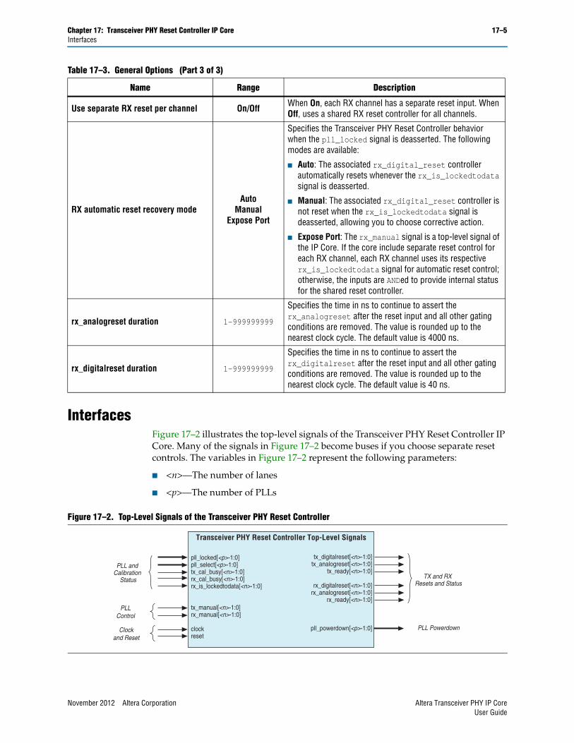
Chapter 17: Transceiver PHY Reset Controller IP Core 17–5Interfaces
InterfacesFigure 17–2 illustrates the top-level signals of the Transceiver PHY Reset Controller IP Core. Many of the signals in Figure 17–2 become buses if you choose separate reset controls. The variables in Figure 17–2 represent the following parameters:
■ <n>—The number of lanes
■ <p>—The number of PLLs
Use separate RX reset per channel On/Off When On, each RX channel has a separate reset input. When Off, uses a shared RX reset controller for all channels.
RX automatic reset recovery modeAuto
ManualExpose Port
Specifies the Transceiver PHY Reset Controller behavior when the pll_locked signal is deasserted. The following modes are available:
■ Auto: The associated rx_digital_reset controller automatically resets whenever the rx_is_lockedtodata signal is deasserted.
■ Manual: The associated rx_digital_reset controller is not reset when the rx_is_lockedtodata signal is deasserted, allowing you to choose corrective action.
■ Expose Port: The rx_manual signal is a top-level signal of the IP Core. If the core include separate reset control for each RX channel, each RX channel uses its respective rx_is_lockedtodata signal for automatic reset control; otherwise, the inputs are ANDed to provide internal status for the shared reset controller.
rx_analogreset duration 1–999999999
Specifies the time in ns to continue to assert the rx_analogreset after the reset input and all other gating conditions are removed. The value is rounded up to the nearest clock cycle. The default value is 4000 ns.
rx_digitalreset duration 1–999999999
Specifies the time in ns to continue to assert the rx_digitalreset after the reset input and all other gating conditions are removed. The value is rounded up to the nearest clock cycle. The default value is 40 ns.
Table 17–3. General Options (Part 3 of 3)
Name Range Description
Figure 17–2. Top-Level Signals of the Transceiver PHY Reset Controller
pll_locked[<p>-1:0]pll_select[<p>-1:0]tx_cal_busy[<n>-1:0]rx_cal_busy[<n>-1:0]rx_is_lockedtodata[<n>-1:0]
tx_manual[<n>-1:0]rx_manual[<n>-1:0]
clockreset
Transceiver PHY Reset Controller Top-Level Signals
tx_digitalreset[<n>-1:0]tx_analogreset[<n>-1:0]
tx_ready[<n>-1:0]
rx_digitalreset[<n>-1:0]rx_analogreset[<n>-1:0]
rx_ready[<n>-1:0]
pll_powerdown[<p>-1:0]
PLL and Calibration
Status
PLL Powerdown
TX and RX Resets and Status
Clockand Reset
PLLControl
November 2012 Altera Corporation Altera Transceiver PHY IP CoreUser Guide
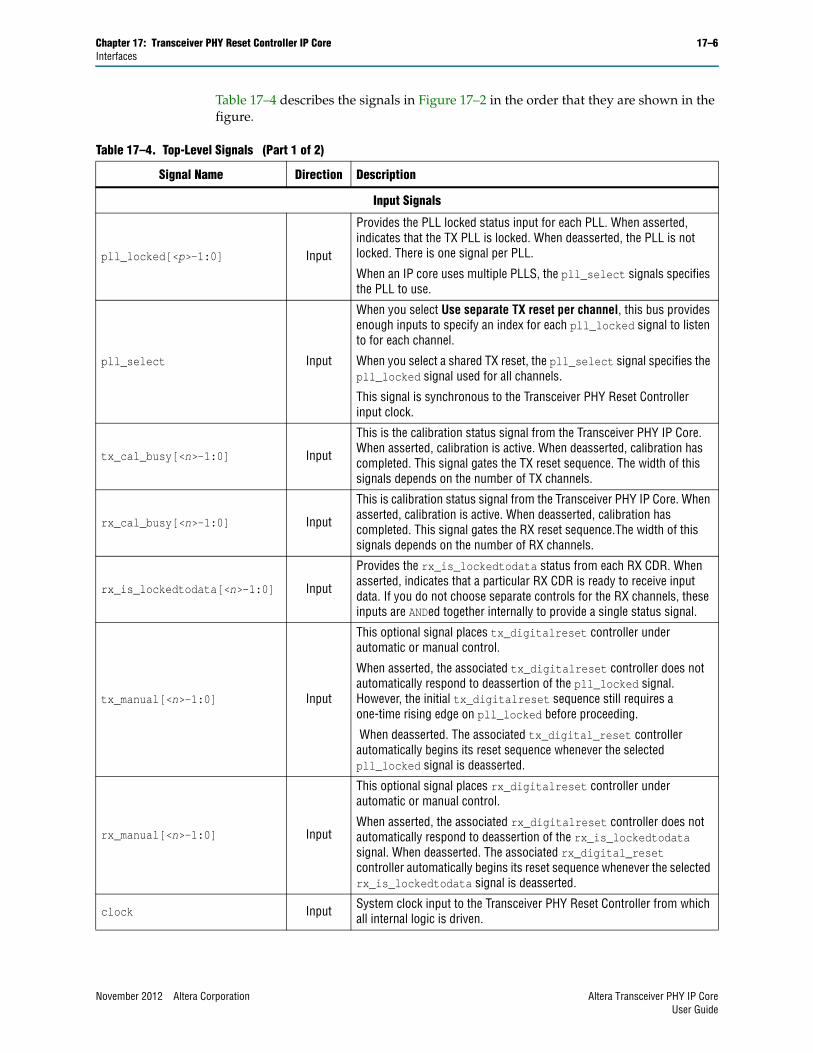
Chapter 17: Transceiver PHY Reset Controller IP Core 17–6Interfaces
Table 17–4 describes the signals in Figure 17–2 in the order that they are shown in the figure.
Table 17–4. Top-Level Signals (Part 1 of 2)
Signal Name Direction Description
Input Signals
pll_locked[<p>-1:0] Input
Provides the PLL locked status input for each PLL. When asserted, indicates that the TX PLL is locked. When deasserted, the PLL is not locked. There is one signal per PLL.
When an IP core uses multiple PLLS, the pll_select signals specifies the PLL to use.
pll_select Input
When you select Use separate TX reset per channel, this bus provides enough inputs to specify an index for each pll_locked signal to listen to for each channel.
When you select a shared TX reset, the pll_select signal specifies the pll_locked signal used for all channels.
This signal is synchronous to the Transceiver PHY Reset Controller input clock.
tx_cal_busy[<n>-1:0] Input
This is the calibration status signal from the Transceiver PHY IP Core. When asserted, calibration is active. When deasserted, calibration has completed. This signal gates the TX reset sequence. The width of this signals depends on the number of TX channels.
rx_cal_busy[<n>-1:0] Input
This is calibration status signal from the Transceiver PHY IP Core. When asserted, calibration is active. When deasserted, calibration has completed. This signal gates the RX reset sequence.The width of this signals depends on the number of RX channels.
rx_is_lockedtodata[<n>-1:0] Input
Provides the rx_is_lockedtodata status from each RX CDR. When asserted, indicates that a particular RX CDR is ready to receive input data. If you do not choose separate controls for the RX channels, these inputs are ANDed together internally to provide a single status signal.
tx_manual[<n>-1:0] Input
This optional signal places tx_digitalreset controller under automatic or manual control.
When asserted, the associated tx_digitalreset controller does not automatically respond to deassertion of the pll_locked signal. However, the initial tx_digitalreset sequence still requires a one-time rising edge on pll_locked before proceeding.
When deasserted. The associated tx_digital_reset controller automatically begins its reset sequence whenever the selected pll_locked signal is deasserted.
rx_manual[<n>-1:0] Input
This optional signal places rx_digitalreset controller under automatic or manual control.
When asserted, the associated rx_digitalreset controller does not automatically respond to deassertion of the rx_is_lockedtodata signal. When deasserted. The associated rx_digital_reset controller automatically begins its reset sequence whenever the selected rx_is_lockedtodata signal is deasserted.
clock Input System clock input to the Transceiver PHY Reset Controller from which all internal logic is driven.
November 2012 Altera Corporation Altera Transceiver PHY IP CoreUser Guide
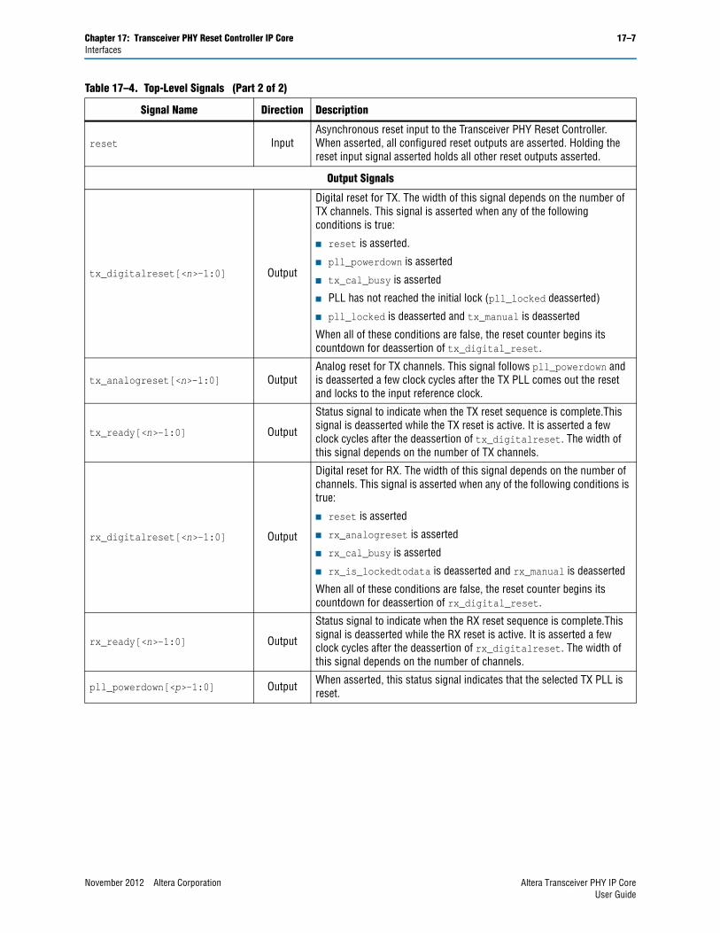
Chapter 17: Transceiver PHY Reset Controller IP Core 17–7Interfaces
reset InputAsynchronous reset input to the Transceiver PHY Reset Controller. When asserted, all configured reset outputs are asserted. Holding the reset input signal asserted holds all other reset outputs asserted.
Output Signals
tx_digitalreset[<n>-1:0] Output
Digital reset for TX. The width of this signal depends on the number of TX channels. This signal is asserted when any of the following conditions is true:
■ reset is asserted.
■ pll_powerdown is asserted
■ tx_cal_busy is asserted
■ PLL has not reached the initial lock (pll_locked deasserted)
■ pll_locked is deasserted and tx_manual is deasserted
When all of these conditions are false, the reset counter begins its countdown for deassertion of tx_digital_reset.
tx_analogreset[<n>-1:0] OutputAnalog reset for TX channels. This signal follows pll_powerdown and is deasserted a few clock cycles after the TX PLL comes out the reset and locks to the input reference clock.
tx_ready[<n>-1:0] Output
Status signal to indicate when the TX reset sequence is complete.This signal is deasserted while the TX reset is active. It is asserted a few clock cycles after the deassertion of tx_digitalreset. The width of this signal depends on the number of TX channels.
rx_digitalreset[<n>-1:0] Output
Digital reset for RX. The width of this signal depends on the number of channels. This signal is asserted when any of the following conditions is true:
■ reset is asserted
■ rx_analogreset is asserted
■ rx_cal_busy is asserted
■ rx_is_lockedtodata is deasserted and rx_manual is deasserted
When all of these conditions are false, the reset counter begins its countdown for deassertion of rx_digital_reset.
rx_ready[<n>-1:0] Output
Status signal to indicate when the RX reset sequence is complete.This signal is deasserted while the RX reset is active. It is asserted a few clock cycles after the deassertion of rx_digitalreset. The width of this signal depends on the number of channels.
pll_powerdown[<p>-1:0] Output When asserted, this status signal indicates that the selected TX PLL is reset.
Table 17–4. Top-Level Signals (Part 2 of 2)
Signal Name Direction Description
November 2012 Altera Corporation Altera Transceiver PHY IP CoreUser Guide
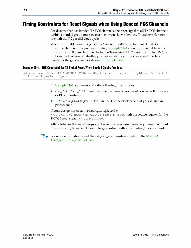
17–8 Chapter 17: Transceiver PHY Reset Controller IP CoreTiming Constraints for Reset Signals when Using Bonded PCS Channels
Timing Constraints for Reset Signals when Using Bonded PCS ChannelsFor designs that use bonded TX PCS channels, the reset signal to all TX PCS channels within a bonded group must meet a maximum skew tolerance. This skew tolerance is one-half the TX parallel clock cycle.
You must provide a Synopsys Design Constraint (SDC) for the reset signals to guarantee that your design meets timing. Example 17–1 shows the general form for this constraint. If your design includes the Transceiver PHY Reset Controller IP Core or the embedded reset controller, you can substitute your instance and interface names for the generic names shown in Example 17–1.
In Example 17–1, you must make the following substitutions:
■ <IP_INSTANCE_NAME>—substitute the name of your reset controller IP instance or PHY IP instance
■ <1/2 coreclk period in ps>—substitute the 1/2 the clock period of your design in picoseconds
If your design has custom reset logic, replace the *<IP_INSTANCE_NAME>*tx_digital_reset*r_reset with the source register for the TX PCS reset signal, tx_digital_reset.
Altera believes that most designs will meet this maximum skew requirement without this constraint; however, it cannot be guaranteed without including this constraint.
f For more information about the set_max_skew constraint, refer to the SDC and TimeQuest API Reference Manual.
Example 17–1. SDC Constraint for TX Digital Reset When Bonded Clocks Are Used
set_max_skew -from *<IP_INSTANCE_NAME>*tx_digitalreset*r_reset -to *pld_pcs_interface* <1/2 coreclk period in ps>
Altera Transceiver PHY IP Core November 2012 Altera CorporationUser Guide
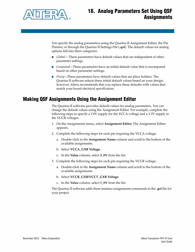
November 2012 Altera Corporation
18. Analog Parameters Set Using QSFAssignments
You specify the analog parameters using the Quartus II Assignment Editor, the Pin Planner, or through the Quartus II Settings File (.qsf). The default values for analog options fall into three categories:
■ Global— These parameters have default values that are independent of other parameter settings.
■ Computed—These parameters have an initial default value that is recomputed based on other parameter settings.
■ Proxy—These parameters have default values that are place holders. The Quartus II software selects these initial default values based on your design; however, Altera recommends that you replace these defaults with values that match your board electrical specification.
Making QSF Assignments Using the Assignment EditorThe Quartus II software provides default values for analog parameters. You can change the default values using the Assignment Editor. For example, complete the following steps to specify a 3.0V supply for the VCCA voltage and a 1.0V supply to the VCCR voltages.
1. On the Assignments menu, select Assignment Editor. The Assignment Editor appears.
2. Complete the following steps for each pin requiring the VCCA voltage:
a. Double-click in the Assignment Name column and scroll to the bottom of the available assignments.
b. Select VCCA_GXB Voltage.
c. In the Value column, select 3_0V from the list.
3. Complete the following steps for each pin requiring the VCCR voltage:
a. Double-click in the Assignment Name column and scroll to the bottom of the available assignments.
b. Select VCCR_GXB/VCCT_GXB Voltage.
c. In the Value column, select 1_0V from the list.
The Quartus II software adds these instance assignments commands to the .qsf file for your project.
Altera Transceiver PHY IP CoreUser Guide
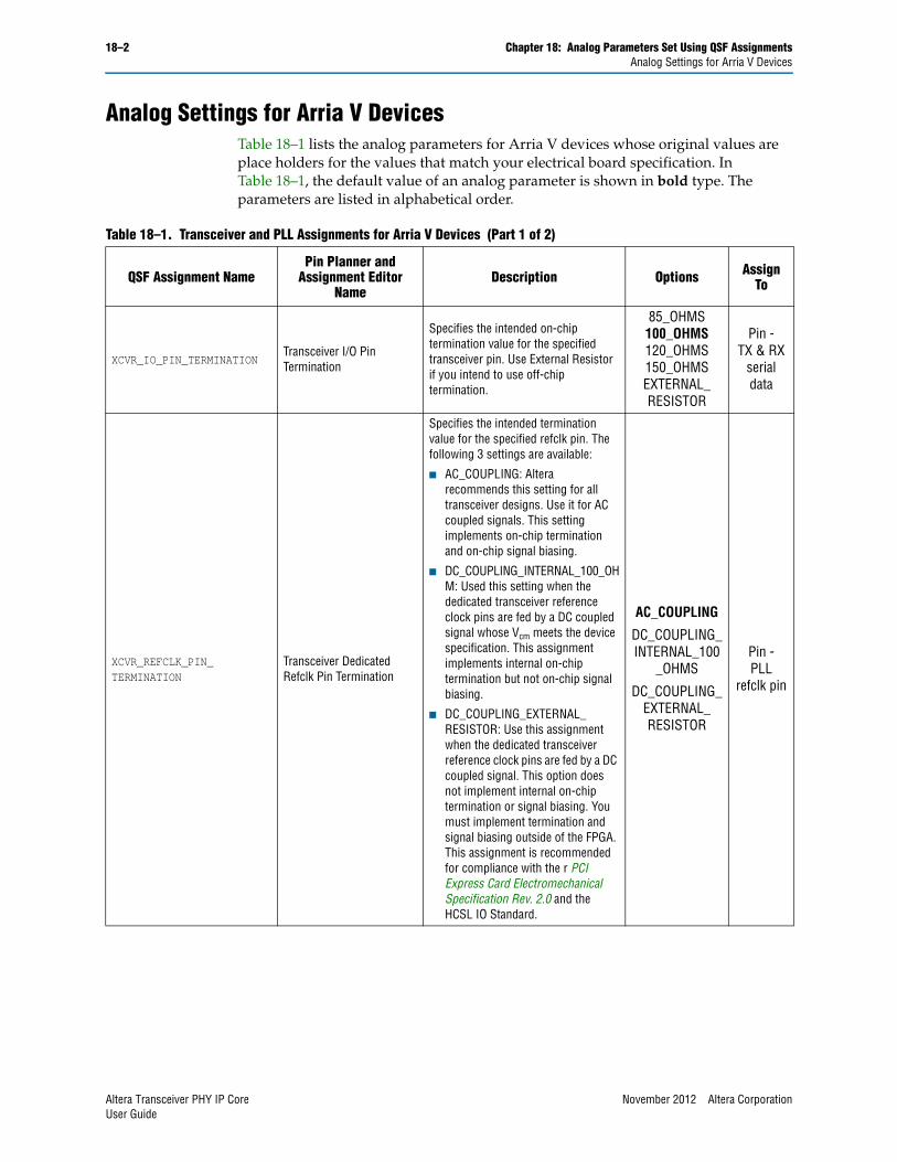
18–2 Chapter 18: Analog Parameters Set Using QSF AssignmentsAnalog Settings for Arria V Devices
Analog Settings for Arria V DevicesTable 18–1 lists the analog parameters for Arria V devices whose original values are place holders for the values that match your electrical board specification. In Table 18–1, the default value of an analog parameter is shown in bold type. The parameters are listed in alphabetical order.
Table 18–1. Transceiver and PLL Assignments for Arria V Devices (Part 1 of 2)
QSF Assignment NamePin Planner and
Assignment Editor Name
Description Options Assign To
XCVR_IO_PIN_TERMINATIONTransceiver I/O Pin Termination
Specifies the intended on-chip termination value for the specified transceiver pin. Use External Resistor if you intend to use off-chip termination.
85_OHMS100_OHMS120_OHMS150_OHMSEXTERNAL_RESISTOR
Pin - TX & RX
serial data
XCVR_REFCLK_PIN_TERMINATION
Transceiver Dedicated Refclk Pin Termination
Specifies the intended termination value for the specified refclk pin. The following 3 settings are available:
■ AC_COUPLING: Altera recommends this setting for all transceiver designs. Use it for AC coupled signals. This setting implements on-chip termination and on-chip signal biasing.
■ DC_COUPLING_INTERNAL_100_OHM: Used this setting when the dedicated transceiver reference clock pins are fed by a DC coupled signal whose Vcm meets the device specification. This assignment implements internal on-chip termination but not on-chip signal biasing.
■ DC_COUPLING_EXTERNAL_RESISTOR: Use this assignment when the dedicated transceiver reference clock pins are fed by a DC coupled signal. This option does not implement internal on-chip termination or signal biasing. You must implement termination and signal biasing outside of the FPGA. This assignment is recommended for compliance with the r PCI Express Card Electromechanical Specification Rev. 2.0 and the HCSL IO Standard.
AC_COUPLING
DC_COUPLING_INTERNAL_100
_OHMS
DC_COUPLING_EXTERNAL_RESISTOR
Pin - PLL
refclk pin
Altera Transceiver PHY IP Core November 2012 Altera CorporationUser Guide
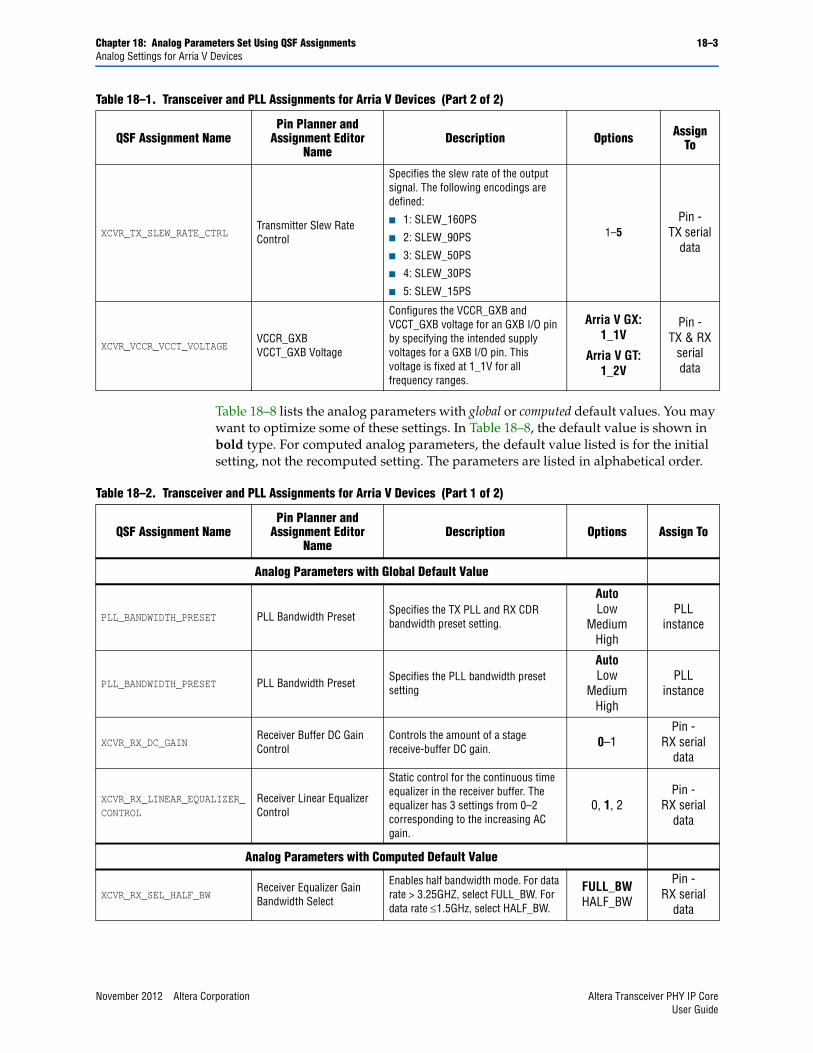
Chapter 18: Analog Parameters Set Using QSF Assignments 18–3Analog Settings for Arria V Devices
Table 18–8 lists the analog parameters with global or computed default values. You may want to optimize some of these settings. In Table 18–8, the default value is shown in bold type. For computed analog parameters, the default value listed is for the initial setting, not the recomputed setting. The parameters are listed in alphabetical order.
XCVR_TX_SLEW_RATE_CTRLTransmitter Slew Rate Control
Specifies the slew rate of the output signal. The following encodings are defined:
■ 1: SLEW_160PS
■ 2: SLEW_90PS
■ 3: SLEW_50PS
■ 4: SLEW_30PS
■ 5: SLEW_15PS
1–5Pin -
TX serial data
XCVR_VCCR_VCCT_VOLTAGEVCCR_GXBVCCT_GXB Voltage
Configures the VCCR_GXB and VCCT_GXB voltage for an GXB I/O pin by specifying the intended supply voltages for a GXB I/O pin. This voltage is fixed at 1_1V for all frequency ranges.
Arria V GX: 1_1V
Arria V GT: 1_2V
Pin - TX & RX
serial data
Table 18–1. Transceiver and PLL Assignments for Arria V Devices (Part 2 of 2)
QSF Assignment NamePin Planner and
Assignment Editor Name
Description Options Assign To
Table 18–2. Transceiver and PLL Assignments for Arria V Devices (Part 1 of 2)
QSF Assignment NamePin Planner and
Assignment Editor Name
Description Options Assign To
Analog Parameters with Global Default Value
PLL_BANDWIDTH_PRESET PLL Bandwidth PresetSpecifies the TX PLL and RX CDR bandwidth preset setting.
AutoLow
MediumHigh
PLL instance
PLL_BANDWIDTH_PRESET PLL Bandwidth Preset Specifies the PLL bandwidth preset setting
AutoLow
MediumHigh
PLL instance
XCVR_RX_DC_GAINReceiver Buffer DC Gain Control
Controls the amount of a stage receive-buffer DC gain. 0–1
Pin - RX serial
data
XCVR_RX_LINEAR_EQUALIZER_CONTROL
Receiver Linear Equalizer Control
Static control for the continuous time equalizer in the receiver buffer. The equalizer has 3 settings from 0–2 corresponding to the increasing AC gain.
0, 1, 2Pin -
RX serial data
Analog Parameters with Computed Default Value
XCVR_RX_SEL_HALF_BWReceiver Equalizer Gain Bandwidth Select
Enables half bandwidth mode. For data rate > 3.25GHZ, select FULL_BW. For data rate 1.5GHz, select HALF_BW.
FULL_BWHALF_BW
Pin - RX serial
data
November 2012 Altera Corporation Altera Transceiver PHY IP CoreUser Guide
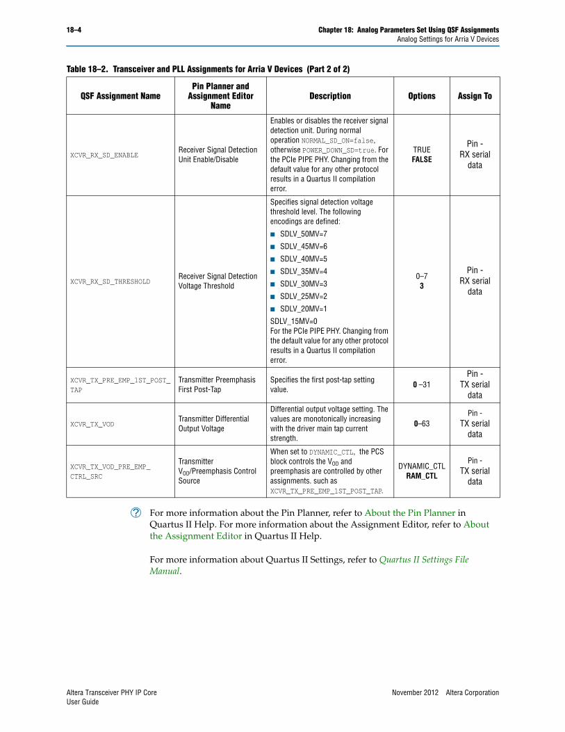
18–4 Chapter 18: Analog Parameters Set Using QSF AssignmentsAnalog Settings for Arria V Devices
h For more information about the Pin Planner, refer to About the Pin Planner in Quartus II Help. For more information about the Assignment Editor, refer to About the Assignment Editor in Quartus II Help.
For more information about Quartus II Settings, refer to Quartus II Settings File Manual.
XCVR_RX_SD_ENABLEReceiver Signal Detection Unit Enable/Disable
Enables or disables the receiver signal detection unit. During normal operation NORMAL_SD_ON=false, otherwise POWER_DOWN_SD=true. For the PCIe PIPE PHY. Changing from the default value for any other protocol results in a Quartus II compilation error.
TRUE FALSE
Pin - RX serial
data
XCVR_RX_SD_THRESHOLDReceiver Signal Detection Voltage Threshold
Specifies signal detection voltage threshold level. The following encodings are defined:
■ SDLV_50MV=7
■ SDLV_45MV=6
■ SDLV_40MV=5
■ SDLV_35MV=4
■ SDLV_30MV=3
■ SDLV_25MV=2
■ SDLV_20MV=1
SDLV_15MV=0For the PCIe PIPE PHY. Changing from the default value for any other protocol results in a Quartus II compilation error.
0–73
Pin - RX serial
data
XCVR_TX_PRE_EMP_1ST_POST_TAP
Transmitter Preemphasis First Post-Tap
Specifies the first post-tap setting value.
0 –31Pin -
TX serial data
XCVR_TX_VODTransmitter Differential Output Voltage
Differential output voltage setting. The values are monotonically increasing with the driver main tap current strength.
0–63Pin -
TX serial data
XCVR_TX_VOD_PRE_EMP_CTRL_SRC
Transmitter VOD/Preemphasis Control Source
When set to DYNAMIC_CTL, the PCS block controls the VOD and preemphasis are controlled by other assignments. such as XCVR_TX_PRE_EMP_1ST_POST_TAP.
DYNAMIC_CTLRAM_CTL
Pin - TX serial
data
Table 18–2. Transceiver and PLL Assignments for Arria V Devices (Part 2 of 2)
QSF Assignment NamePin Planner and
Assignment Editor Name
Description Options Assign To
Altera Transceiver PHY IP Core November 2012 Altera CorporationUser Guide
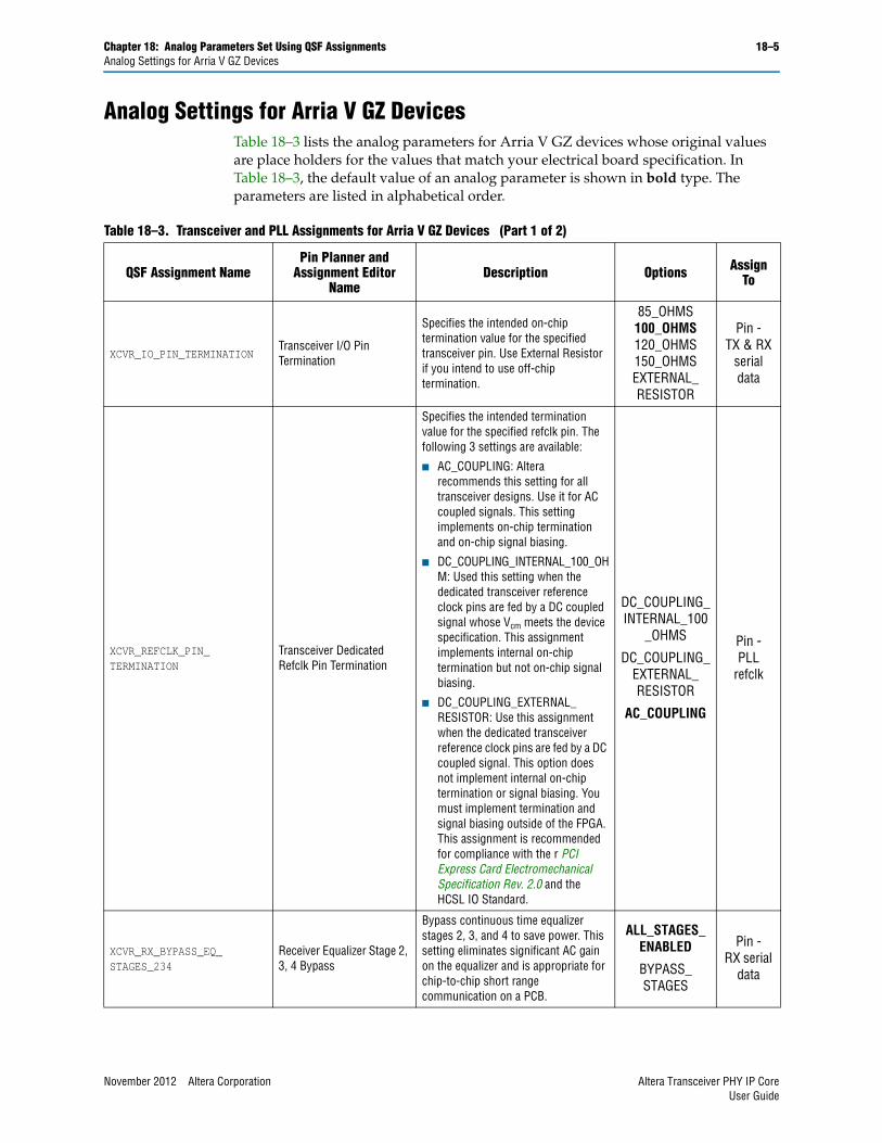
Chapter 18: Analog Parameters Set Using QSF Assignments 18–5Analog Settings for Arria V GZ Devices
Analog Settings for Arria V GZ DevicesTable 18–3 lists the analog parameters for Arria V GZ devices whose original values are place holders for the values that match your electrical board specification. In Table 18–3, the default value of an analog parameter is shown in bold type. The parameters are listed in alphabetical order.
Table 18–3. Transceiver and PLL Assignments for Arria V GZ Devices (Part 1 of 2)
QSF Assignment NamePin Planner and
Assignment Editor Name
Description Options Assign To
XCVR_IO_PIN_TERMINATIONTransceiver I/O Pin Termination
Specifies the intended on-chip termination value for the specified transceiver pin. Use External Resistor if you intend to use off-chip termination.
85_OHMS100_OHMS120_OHMS150_OHMSEXTERNAL_RESISTOR
Pin - TX & RX
serial data
XCVR_REFCLK_PIN_TERMINATION
Transceiver Dedicated Refclk Pin Termination
Specifies the intended termination value for the specified refclk pin. The following 3 settings are available:
■ AC_COUPLING: Altera recommends this setting for all transceiver designs. Use it for AC coupled signals. This setting implements on-chip termination and on-chip signal biasing.
■ DC_COUPLING_INTERNAL_100_OHM: Used this setting when the dedicated transceiver reference clock pins are fed by a DC coupled signal whose Vcm meets the device specification. This assignment implements internal on-chip termination but not on-chip signal biasing.
■ DC_COUPLING_EXTERNAL_RESISTOR: Use this assignment when the dedicated transceiver reference clock pins are fed by a DC coupled signal. This option does not implement internal on-chip termination or signal biasing. You must implement termination and signal biasing outside of the FPGA. This assignment is recommended for compliance with the r PCI Express Card Electromechanical Specification Rev. 2.0 and the HCSL IO Standard.
DC_COUPLING_INTERNAL_100
_OHMS
DC_COUPLING_EXTERNAL_RESISTOR
AC_COUPLING
Pin - PLL
refclk
XCVR_RX_BYPASS_EQ_STAGES_234
Receiver Equalizer Stage 2, 3, 4 Bypass
Bypass continuous time equalizer stages 2, 3, and 4 to save power. This setting eliminates significant AC gain on the equalizer and is appropriate for chip-to-chip short range communication on a PCB.
ALL_STAGES_ENABLED
BYPASS_STAGES
Pin - RX serial
data
November 2012 Altera Corporation Altera Transceiver PHY IP CoreUser Guide
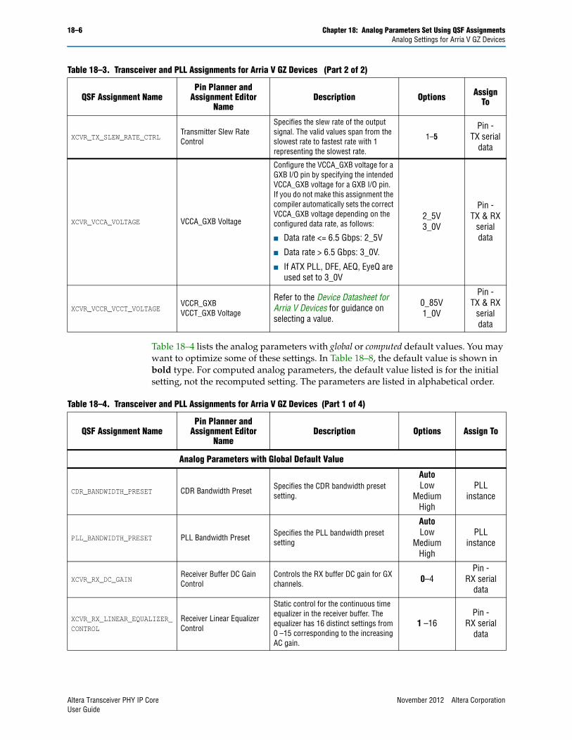
18–6 Chapter 18: Analog Parameters Set Using QSF AssignmentsAnalog Settings for Arria V GZ Devices
Table 18–4 lists the analog parameters with global or computed default values. You may want to optimize some of these settings. In Table 18–8, the default value is shown in bold type. For computed analog parameters, the default value listed is for the initial setting, not the recomputed setting. The parameters are listed in alphabetical order.
XCVR_TX_SLEW_RATE_CTRLTransmitter Slew Rate Control
Specifies the slew rate of the output signal. The valid values span from the slowest rate to fastest rate with 1 representing the slowest rate.
1–5Pin -
TX serial data
XCVR_VCCA_VOLTAGE VCCA_GXB Voltage
Configure the VCCA_GXB voltage for a GXB I/O pin by specifying the intended VCCA_GXB voltage for a GXB I/O pin. If you do not make this assignment the compiler automatically sets the correct VCCA_GXB voltage depending on the configured data rate, as follows:
■ Data rate <= 6.5 Gbps: 2_5V
■ Data rate > 6.5 Gbps: 3_0V.
■ If ATX PLL, DFE, AEQ, EyeQ are used set to 3_0V
2_5V3_0V
Pin - TX & RX
serial data
XCVR_VCCR_VCCT_VOLTAGEVCCR_GXBVCCT_GXB Voltage
Refer to the Device Datasheet for Arria V Devices for guidance on selecting a value.
0_85V1_0V
Pin - TX & RX
serial data
Table 18–3. Transceiver and PLL Assignments for Arria V GZ Devices (Part 2 of 2)
QSF Assignment NamePin Planner and
Assignment Editor Name
Description Options Assign To
Table 18–4. Transceiver and PLL Assignments for Arria V GZ Devices (Part 1 of 4)
QSF Assignment NamePin Planner and
Assignment Editor Name
Description Options Assign To
Analog Parameters with Global Default Value
CDR_BANDWIDTH_PRESET CDR Bandwidth Preset Specifies the CDR bandwidth preset setting.
AutoLow
MediumHigh
PLL instance
PLL_BANDWIDTH_PRESET PLL Bandwidth Preset Specifies the PLL bandwidth preset setting
AutoLow
MediumHigh
PLL instance
XCVR_RX_DC_GAINReceiver Buffer DC Gain Control
Controls the RX buffer DC gain for GX channels. 0–4
Pin - RX serial
data
XCVR_RX_LINEAR_EQUALIZER_CONTROL
Receiver Linear Equalizer Control
Static control for the continuous time equalizer in the receiver buffer. The equalizer has 16 distinct settings from 0 –15 corresponding to the increasing AC gain.
1 –16Pin -
RX serial data
Altera Transceiver PHY IP Core November 2012 Altera CorporationUser Guide
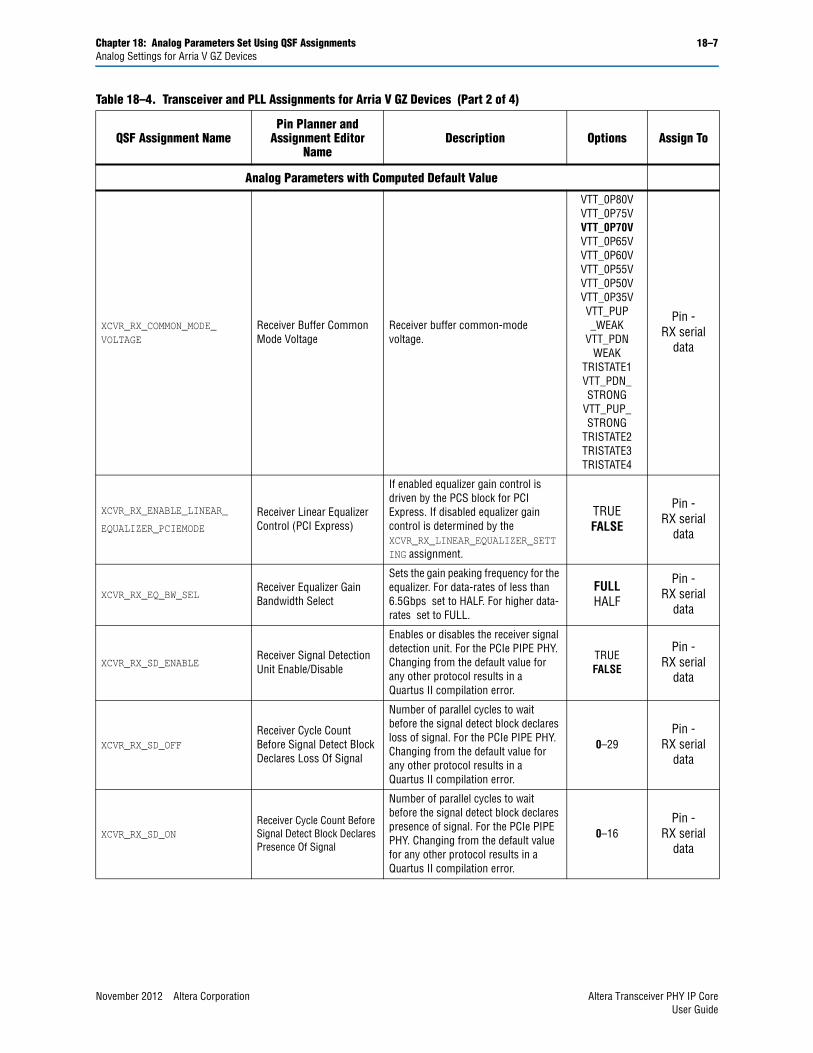
Chapter 18: Analog Parameters Set Using QSF Assignments 18–7Analog Settings for Arria V GZ Devices
Analog Parameters with Computed Default Value
XCVR_RX_COMMON_MODE_VOLTAGE
Receiver Buffer Common Mode Voltage
Receiver buffer common-mode voltage.
VTT_0P80VVTT_0P75VVTT_0P70VVTT_0P65VVTT_0P60VVTT_0P55VVTT_0P50VVTT_0P35VVTT_PUP_WEAK
VTT_PDNWEAK
TRISTATE1VTT_PDN_STRONG
VTT_PUP_STRONG
TRISTATE2TRISTATE3TRISTATE4
Pin - RX serial
data
XCVR_RX_ENABLE_LINEAR_
EQUALIZER_PCIEMODE
Receiver Linear Equalizer Control (PCI Express)
If enabled equalizer gain control is driven by the PCS block for PCI Express. If disabled equalizer gain control is determined by the XCVR_RX_LINEAR_EQUALIZER_SETTING assignment.
TRUEFALSE
Pin - RX serial
data
XCVR_RX_EQ_BW_SELReceiver Equalizer Gain Bandwidth Select
Sets the gain peaking frequency for the equalizer. For data-rates of less than 6.5Gbps set to HALF. For higher data-rates set to FULL.
FULLHALF
Pin - RX serial
data
XCVR_RX_SD_ENABLEReceiver Signal Detection Unit Enable/Disable
Enables or disables the receiver signal detection unit. For the PCIe PIPE PHY. Changing from the default value for any other protocol results in a Quartus II compilation error.
TRUE FALSE
Pin - RX serial
data
XCVR_RX_SD_OFFReceiver Cycle Count Before Signal Detect Block Declares Loss Of Signal
Number of parallel cycles to wait before the signal detect block declares loss of signal. For the PCIe PIPE PHY. Changing from the default value for any other protocol results in a Quartus II compilation error.
0–29Pin -
RX serial data
XCVR_RX_SD_ONReceiver Cycle Count Before Signal Detect Block Declares Presence Of Signal
Number of parallel cycles to wait before the signal detect block declares presence of signal. For the PCIe PIPE PHY. Changing from the default value for any other protocol results in a Quartus II compilation error.
0–16Pin -
RX serial data
Table 18–4. Transceiver and PLL Assignments for Arria V GZ Devices (Part 2 of 4)
QSF Assignment NamePin Planner and
Assignment Editor Name
Description Options Assign To
November 2012 Altera Corporation Altera Transceiver PHY IP CoreUser Guide
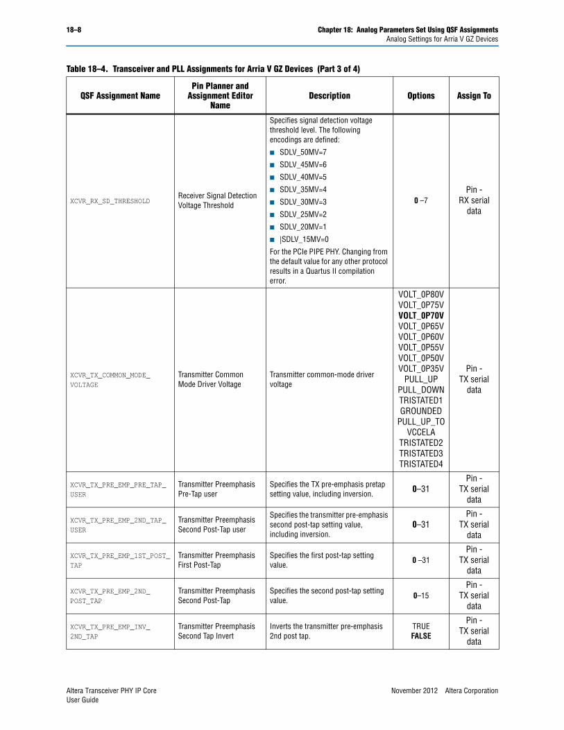
18–8 Chapter 18: Analog Parameters Set Using QSF AssignmentsAnalog Settings for Arria V GZ Devices
XCVR_RX_SD_THRESHOLDReceiver Signal Detection Voltage Threshold
Specifies signal detection voltage threshold level. The following encodings are defined:
■ SDLV_50MV=7
■ SDLV_45MV=6
■ SDLV_40MV=5
■ SDLV_35MV=4
■ SDLV_30MV=3
■ SDLV_25MV=2
■ SDLV_20MV=1
■ |SDLV_15MV=0
For the PCIe PIPE PHY. Changing from the default value for any other protocol results in a Quartus II compilation error.
0 –7Pin -
RX serial data
XCVR_TX_COMMON_MODE_VOLTAGE
Transmitter Common Mode Driver Voltage
Transmitter common-mode driver voltage
VOLT_0P80VVOLT_0P75VVOLT_0P70VVOLT_0P65VVOLT_0P60VVOLT_0P55VVOLT_0P50VVOLT_0P35V
PULL_UPPULL_DOWNTRISTATED1GROUNDED
PULL_UP_TOVCCELA
TRISTATED2TRISTATED3TRISTATED4
Pin - TX serial
data
XCVR_TX_PRE_EMP_PRE_TAP_USER
Transmitter Preemphasis Pre-Tap user
Specifies the TX pre-emphasis pretap setting value, including inversion. 0–31
Pin - TX serial
data
XCVR_TX_PRE_EMP_2ND_TAP_USER
Transmitter Preemphasis Second Post-Tap user
Specifies the transmitter pre-emphasis second post-tap setting value, including inversion.
0–31Pin -
TX serial data
XCVR_TX_PRE_EMP_1ST_POST_TAP
Transmitter Preemphasis First Post-Tap
Specifies the first post-tap setting value. 0 –31
Pin - TX serial
data
XCVR_TX_PRE_EMP_2ND_POST_TAP
Transmitter Preemphasis Second Post-Tap
Specifies the second post-tap setting value. 0–15
Pin - TX serial
data
XCVR_TX_PRE_EMP_INV_2ND_TAP
Transmitter Preemphasis Second Tap Invert
Inverts the transmitter pre-emphasis 2nd post tap.
TRUEFALSE
Pin - TX serial
data
Table 18–4. Transceiver and PLL Assignments for Arria V GZ Devices (Part 3 of 4)
QSF Assignment NamePin Planner and
Assignment Editor Name
Description Options Assign To
Altera Transceiver PHY IP Core November 2012 Altera CorporationUser Guide
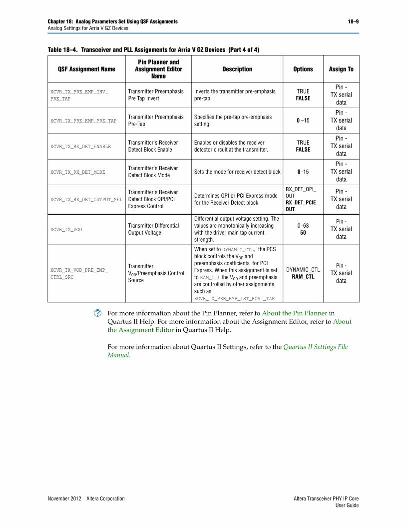
Chapter 18: Analog Parameters Set Using QSF Assignments 18–9Analog Settings for Arria V GZ Devices
h For more information about the Pin Planner, refer to About the Pin Planner in Quartus II Help. For more information about the Assignment Editor, refer to About the Assignment Editor in Quartus II Help.
For more information about Quartus II Settings, refer to the Quartus II Settings File Manual.
XCVR_TX_PRE_EMP_INV_PRE_TAP
Transmitter Preemphasis Pre Tap Invert
Inverts the transmitter pre-emphasis pre-tap.
TRUEFALSE
Pin - TX serial
data
XCVR_TX_PRE_EMP_PRE_TAPTransmitter PreemphasisPre-Tap
Specifies the pre-tap pre-emphasis setting.
0 –15Pin -
TX serial data
XCVR_TX_RX_DET_ENABLETransmitter's Receiver Detect Block Enable
Enables or disables the receiver detector circuit at the transmitter.
TRUEFALSE
Pin - TX serial
data
XCVR_TX_RX_DET_MODETransmitter's Receiver Detect Block Mode Sets the mode for receiver detect block 0–15
Pin - TX serial
data
XCVR_TX_RX_DET_OUTPUT_SELTransmitter's Receiver Detect Block QPI/PCI Express Control
Determines QPI or PCI Express mode for the Receiver Detect block.
RX_DET_QPI_OUT RX_DET_PCIE_OUT
Pin - TX serial
data
XCVR_TX_VODTransmitter Differential Output Voltage
Differential output voltage setting. The values are monotonically increasing with the driver main tap current strength.
0–6350
Pin - TX serial
data
XCVR_TX_VOD_PRE_EMP_CTRL_SRC
Transmitter VOD/Preemphasis Control Source
When set to DYNAMIC_CTL, the PCS block controls the VOD and preemphasis coefficients for PCI Express. When this assignment is set to RAM_CTL the VOD and preemphasis are controlled by other assignments, such as XCVR_TX_PRE_EMP_1ST_POST_TAP.
DYNAMIC_CTLRAM_CTL
Pin - TX serial
data
Table 18–4. Transceiver and PLL Assignments for Arria V GZ Devices (Part 4 of 4)
QSF Assignment NamePin Planner and
Assignment Editor Name
Description Options Assign To
November 2012 Altera Corporation Altera Transceiver PHY IP CoreUser Guide
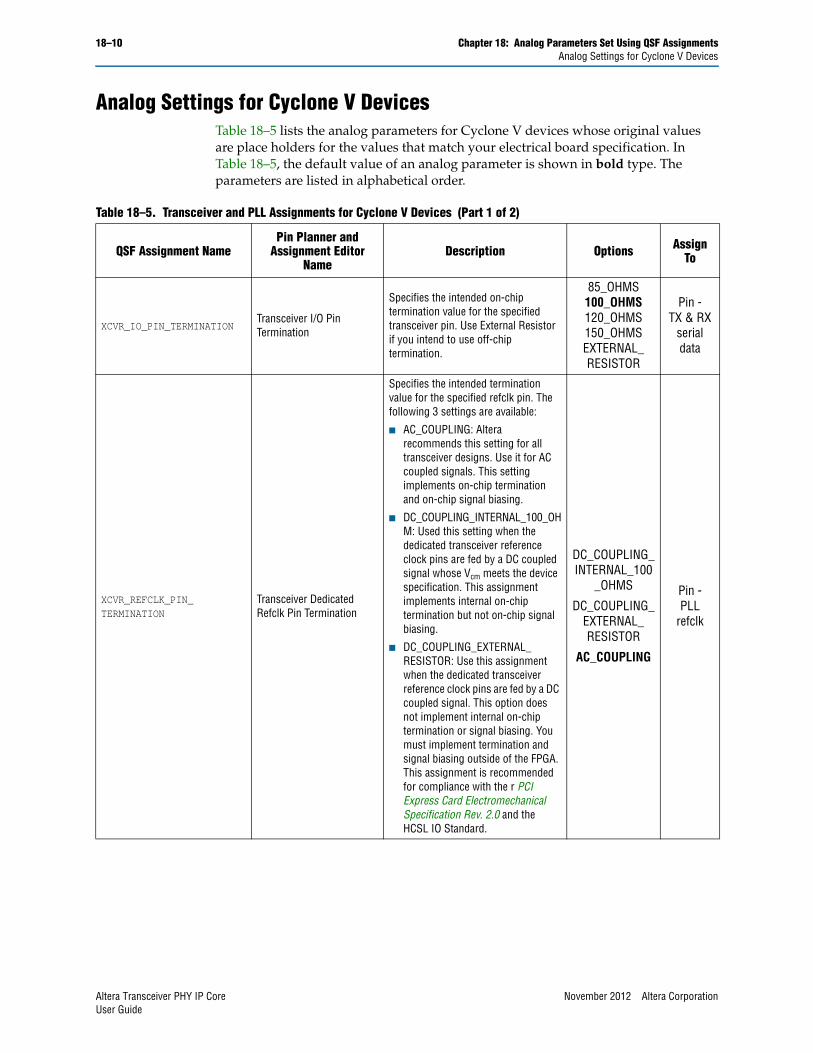
18–10 Chapter 18: Analog Parameters Set Using QSF AssignmentsAnalog Settings for Cyclone V Devices
Analog Settings for Cyclone V DevicesTable 18–5 lists the analog parameters for Cyclone V devices whose original values are place holders for the values that match your electrical board specification. In Table 18–5, the default value of an analog parameter is shown in bold type. The parameters are listed in alphabetical order.
Table 18–5. Transceiver and PLL Assignments for Cyclone V Devices (Part 1 of 2)
QSF Assignment NamePin Planner and
Assignment Editor Name
Description Options Assign To
XCVR_IO_PIN_TERMINATIONTransceiver I/O Pin Termination
Specifies the intended on-chip termination value for the specified transceiver pin. Use External Resistor if you intend to use off-chip termination.
85_OHMS100_OHMS120_OHMS150_OHMSEXTERNAL_RESISTOR
Pin - TX & RX
serial data
XCVR_REFCLK_PIN_TERMINATION
Transceiver Dedicated Refclk Pin Termination
Specifies the intended termination value for the specified refclk pin. The following 3 settings are available:
■ AC_COUPLING: Altera recommends this setting for all transceiver designs. Use it for AC coupled signals. This setting implements on-chip termination and on-chip signal biasing.
■ DC_COUPLING_INTERNAL_100_OHM: Used this setting when the dedicated transceiver reference clock pins are fed by a DC coupled signal whose Vcm meets the device specification. This assignment implements internal on-chip termination but not on-chip signal biasing.
■ DC_COUPLING_EXTERNAL_RESISTOR: Use this assignment when the dedicated transceiver reference clock pins are fed by a DC coupled signal. This option does not implement internal on-chip termination or signal biasing. You must implement termination and signal biasing outside of the FPGA. This assignment is recommended for compliance with the r PCI Express Card Electromechanical Specification Rev. 2.0 and the HCSL IO Standard.
DC_COUPLING_INTERNAL_100
_OHMS
DC_COUPLING_EXTERNAL_RESISTOR
AC_COUPLING
Pin - PLL
refclk
Altera Transceiver PHY IP Core November 2012 Altera CorporationUser Guide
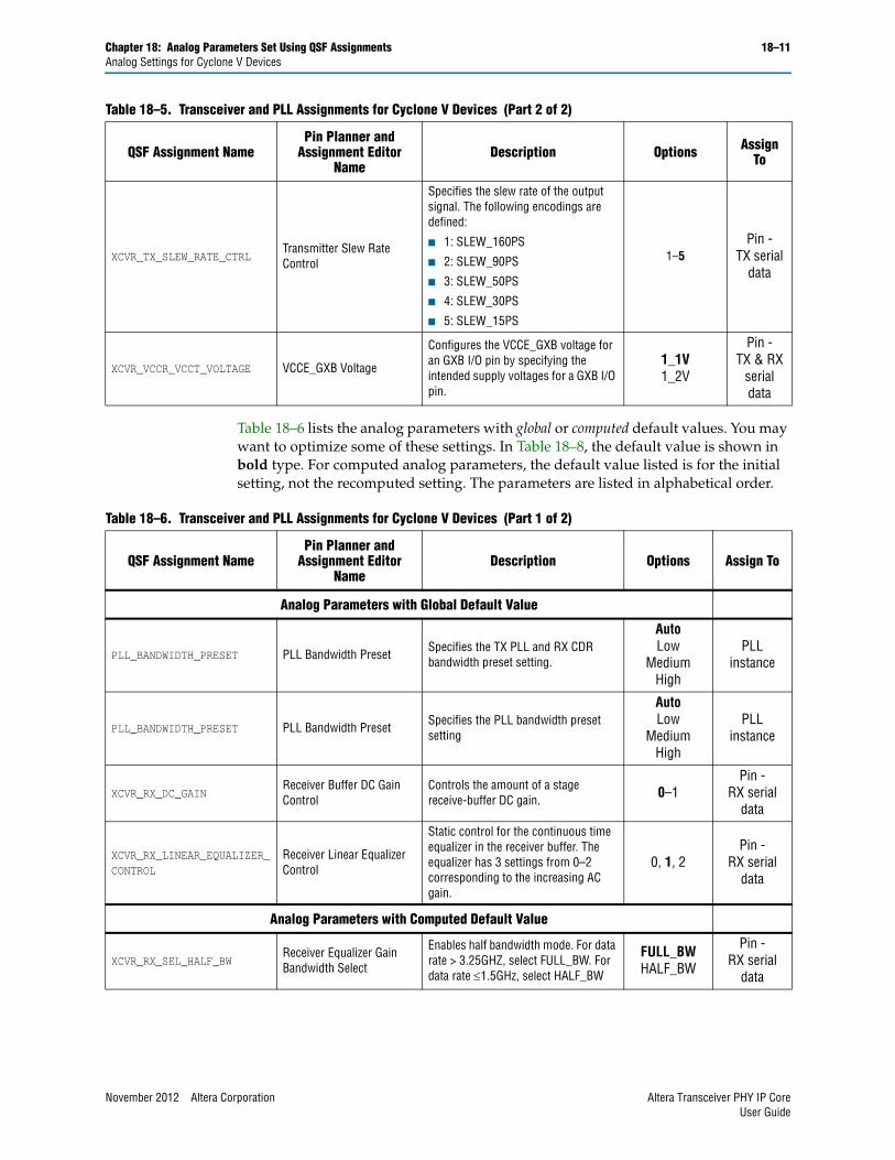
Chapter 18: Analog Parameters Set Using QSF Assignments 18–11Analog Settings for Cyclone V Devices
Table 18–6 lists the analog parameters with global or computed default values. You may want to optimize some of these settings. In Table 18–8, the default value is shown in bold type. For computed analog parameters, the default value listed is for the initial setting, not the recomputed setting. The parameters are listed in alphabetical order.
XCVR_TX_SLEW_RATE_CTRLTransmitter Slew Rate Control
Specifies the slew rate of the output signal. The following encodings are defined:
■ 1: SLEW_160PS
■ 2: SLEW_90PS
■ 3: SLEW_50PS
■ 4: SLEW_30PS
■ 5: SLEW_15PS
1–5Pin -
TX serial data
XCVR_VCCR_VCCT_VOLTAGE VCCE_GXB Voltage
Configures the VCCE_GXB voltage for an GXB I/O pin by specifying the intended supply voltages for a GXB I/O pin.
1_1V1_2V
Pin - TX & RX
serial data
Table 18–5. Transceiver and PLL Assignments for Cyclone V Devices (Part 2 of 2)
QSF Assignment NamePin Planner and
Assignment Editor Name
Description Options Assign To
Table 18–6. Transceiver and PLL Assignments for Cyclone V Devices (Part 1 of 2)
QSF Assignment NamePin Planner and
Assignment Editor Name
Description Options Assign To
Analog Parameters with Global Default Value
PLL_BANDWIDTH_PRESET PLL Bandwidth PresetSpecifies the TX PLL and RX CDR bandwidth preset setting.
AutoLow
MediumHigh
PLL instance
PLL_BANDWIDTH_PRESET PLL Bandwidth PresetSpecifies the PLL bandwidth preset setting
AutoLow
MediumHigh
PLL instance
XCVR_RX_DC_GAINReceiver Buffer DC Gain Control
Controls the amount of a stage receive-buffer DC gain. 0–1
Pin - RX serial
data
XCVR_RX_LINEAR_EQUALIZER_CONTROL
Receiver Linear Equalizer Control
Static control for the continuous time equalizer in the receiver buffer. The equalizer has 3 settings from 0–2 corresponding to the increasing AC gain.
0, 1, 2Pin -
RX serial data
Analog Parameters with Computed Default Value
XCVR_RX_SEL_HALF_BWReceiver Equalizer Gain Bandwidth Select
Enables half bandwidth mode. For data rate > 3.25GHZ, select FULL_BW. For data rate 1.5GHz, select HALF_BW
FULL_BWHALF_BW
Pin - RX serial
data
November 2012 Altera Corporation Altera Transceiver PHY IP CoreUser Guide
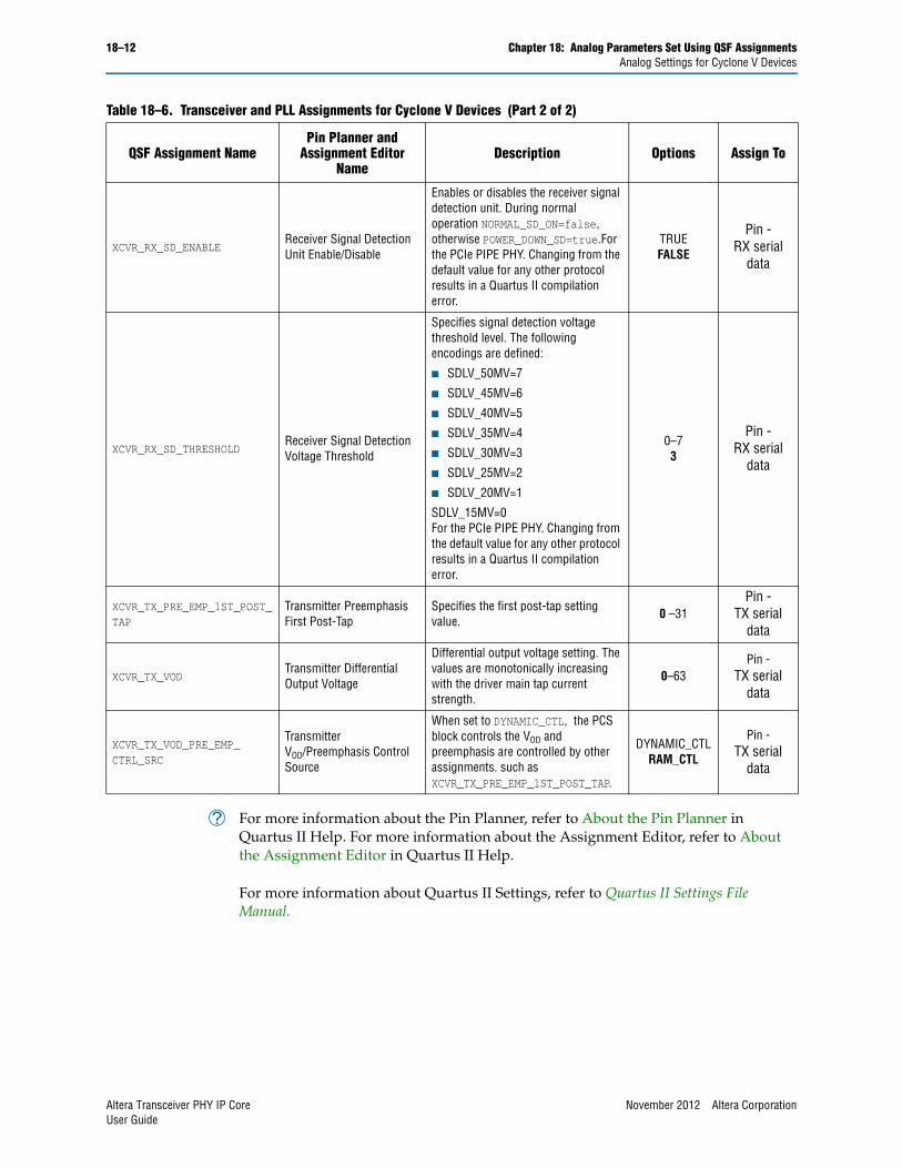
18–12 Chapter 18: Analog Parameters Set Using QSF AssignmentsAnalog Settings for Cyclone V Devices
h For more information about the Pin Planner, refer to About the Pin Planner in Quartus II Help. For more information about the Assignment Editor, refer to About the Assignment Editor in Quartus II Help.
For more information about Quartus II Settings, refer to Quartus II Settings File Manual.
XCVR_RX_SD_ENABLEReceiver Signal Detection Unit Enable/Disable
Enables or disables the receiver signal detection unit. During normal operation NORMAL_SD_ON=false, otherwise POWER_DOWN_SD=true.For the PCIe PIPE PHY. Changing from the default value for any other protocol results in a Quartus II compilation error.
TRUE FALSE
Pin - RX serial
data
XCVR_RX_SD_THRESHOLDReceiver Signal Detection Voltage Threshold
Specifies signal detection voltage threshold level. The following encodings are defined:
■ SDLV_50MV=7
■ SDLV_45MV=6
■ SDLV_40MV=5
■ SDLV_35MV=4
■ SDLV_30MV=3
■ SDLV_25MV=2
■ SDLV_20MV=1
SDLV_15MV=0For the PCIe PIPE PHY. Changing from the default value for any other protocol results in a Quartus II compilation error.
0–73
Pin - RX serial
data
XCVR_TX_PRE_EMP_1ST_POST_TAP
Transmitter Preemphasis First Post-Tap
Specifies the first post-tap setting value.
0 –31Pin -
TX serial data
XCVR_TX_VODTransmitter Differential Output Voltage
Differential output voltage setting. The values are monotonically increasing with the driver main tap current strength.
0–63Pin -
TX serial data
XCVR_TX_VOD_PRE_EMP_CTRL_SRC
Transmitter VOD/Preemphasis Control Source
When set to DYNAMIC_CTL, the PCS block controls the VOD and preemphasis are controlled by other assignments. such as XCVR_TX_PRE_EMP_1ST_POST_TAP.
DYNAMIC_CTLRAM_CTL
Pin - TX serial
data
Table 18–6. Transceiver and PLL Assignments for Cyclone V Devices (Part 2 of 2)
QSF Assignment NamePin Planner and
Assignment Editor Name
Description Options Assign To
Altera Transceiver PHY IP Core November 2012 Altera CorporationUser Guide
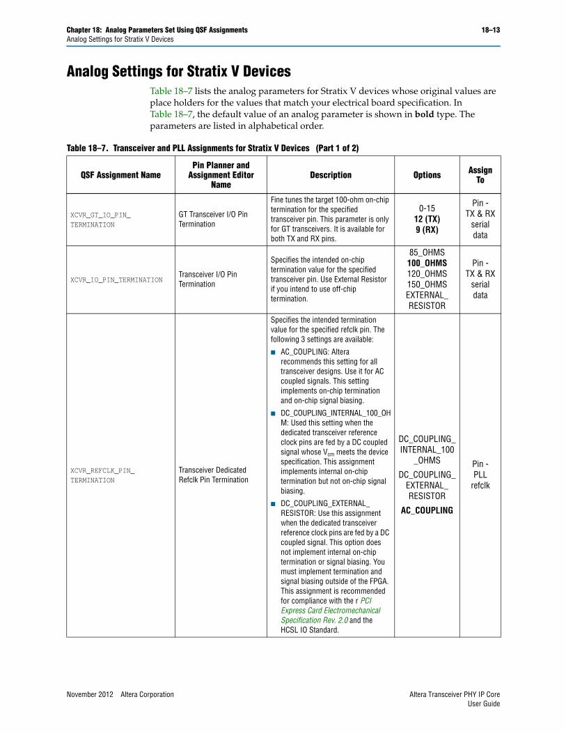
Chapter 18: Analog Parameters Set Using QSF Assignments 18–13Analog Settings for Stratix V Devices
Analog Settings for Stratix V DevicesTable 18–7 lists the analog parameters for Stratix V devices whose original values are place holders for the values that match your electrical board specification. In Table 18–7, the default value of an analog parameter is shown in bold type. The parameters are listed in alphabetical order.
Table 18–7. Transceiver and PLL Assignments for Stratix V Devices (Part 1 of 2)
QSF Assignment NamePin Planner and
Assignment Editor Name
Description Options Assign To
XCVR_GT_IO_PIN_TERMINATION
GT Transceiver I/O Pin Termination
Fine tunes the target 100-ohm on-chip termination for the specified transceiver pin. This parameter is only for GT transceivers. It is available for both TX and RX pins.
0-1512 (TX)9 (RX)
Pin - TX & RX
serial data
XCVR_IO_PIN_TERMINATIONTransceiver I/O Pin Termination
Specifies the intended on-chip termination value for the specified transceiver pin. Use External Resistor if you intend to use off-chip termination.
85_OHMS100_OHMS120_OHMS150_OHMSEXTERNAL_RESISTOR
Pin - TX & RX
serial data
XCVR_REFCLK_PIN_TERMINATION
Transceiver Dedicated Refclk Pin Termination
Specifies the intended termination value for the specified refclk pin. The following 3 settings are available:
■ AC_COUPLING: Altera recommends this setting for all transceiver designs. Use it for AC coupled signals. This setting implements on-chip termination and on-chip signal biasing.
■ DC_COUPLING_INTERNAL_100_OHM: Used this setting when the dedicated transceiver reference clock pins are fed by a DC coupled signal whose Vcm meets the device specification. This assignment implements internal on-chip termination but not on-chip signal biasing.
■ DC_COUPLING_EXTERNAL_RESISTOR: Use this assignment when the dedicated transceiver reference clock pins are fed by a DC coupled signal. This option does not implement internal on-chip termination or signal biasing. You must implement termination and signal biasing outside of the FPGA. This assignment is recommended for compliance with the r PCI Express Card Electromechanical Specification Rev. 2.0 and the HCSL IO Standard.
DC_COUPLING_INTERNAL_100
_OHMS
DC_COUPLING_EXTERNAL_RESISTOR
AC_COUPLING
Pin - PLL
refclk
November 2012 Altera Corporation Altera Transceiver PHY IP CoreUser Guide
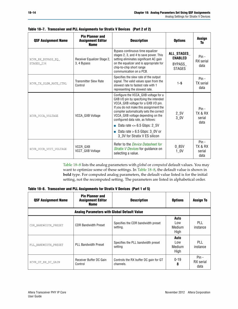
18–14 Chapter 18: Analog Parameters Set Using QSF AssignmentsAnalog Settings for Stratix V Devices
Table 18–8 lists the analog parameters with global or computed default values. You may want to optimize some of these settings. In Table 18–8, the default value is shown in bold type. For computed analog parameters, the default value listed is for the initial setting, not the recomputed setting. The parameters are listed in alphabetical order.
XCVR_RX_BYPASS_EQ_STAGES_234
Receiver Equalizer Stage 2, 3, 4 Bypass
Bypass continuous time equalizer stages 2, 3, and 4 to save power. This setting eliminates significant AC gain on the equalizer and is appropriate for chip-to-chip short range communication on a PCB.
ALL_STAGES_ENABLED
BYPASS_STAGES
Pin - RX serial
data
XCVR_TX_SLEW_RATE_CTRLTransmitter Slew Rate Control
Specifies the slew rate of the output signal. The valid values span from the slowest rate to fastest rate with 1 representing the slowest rate.
1–5Pin -
TX serial data
XCVR_VCCA_VOLTAGE VCCA_GXB Voltage
Configure the VCCA_GXB voltage for a GXB I/O pin by specifying the intended VCCA_GXB voltage for a GXB I/O pin. If you do not make this assignment the compiler automatically sets the correct VCCA_GXB voltage depending on the configured data rate, as follows:
■ Data rate <= 6.5 Gbps: 2_5V
■ Data rate > 6.5 Gbps: 3_0V or 3_3V for Stratix V ES silicon
2_5V3_0V
Pin - TX & RX
serial data
XCVR_VCCR_VCCT_VOLTAGEVCCR_GXBVCCT_GXB Voltage
Refer to the Device Datasheet for Stratix V Devices for guidance on selecting a value.
0_85V1_0V
Pin - TX & RX
serial data
Table 18–7. Transceiver and PLL Assignments for Stratix V Devices (Part 2 of 2)
QSF Assignment NamePin Planner and
Assignment Editor Name
Description Options Assign To
Table 18–8. Transceiver and PLL Assignments for Stratix V Devices (Part 1 of 5)
QSF Assignment NamePin Planner and
Assignment Editor Name
Description Options Assign To
Analog Parameters with Global Default Value
CDR_BANDWIDTH_PRESET CDR Bandwidth Preset Specifies the CDR bandwidth preset setting.
AutoLow
MediumHigh
PLL instance
PLL_BANDWIDTH_PRESET PLL Bandwidth PresetSpecifies the PLL bandwidth preset setting
AutoLow
MediumHigh
PLL instance
XCVR_GT_RX_DC_GAINReceiver Buffer DC Gain Control
Controls the RX buffer DC gain for GT channels.
0-198
Pin - RX serial
data
Altera Transceiver PHY IP Core November 2012 Altera CorporationUser Guide
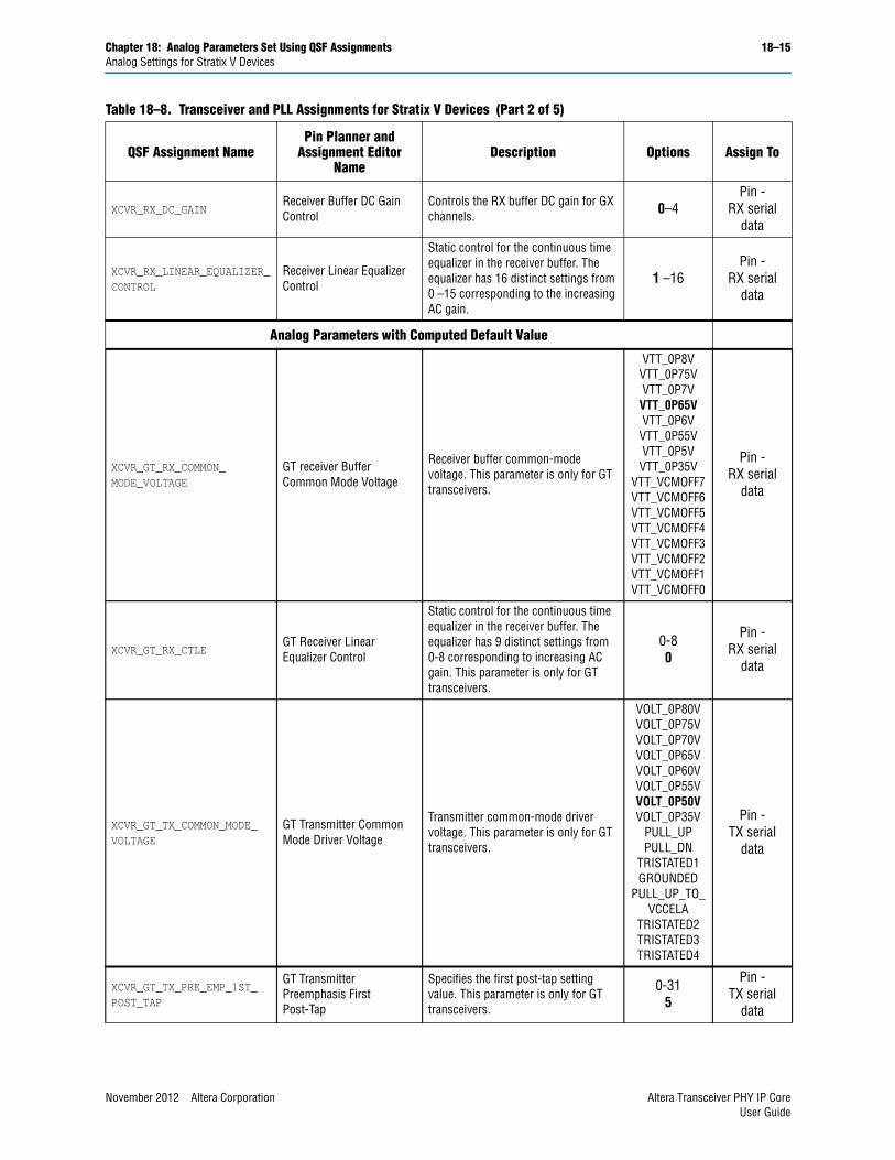
Chapter 18: Analog Parameters Set Using QSF Assignments 18–15Analog Settings for Stratix V Devices
XCVR_RX_DC_GAINReceiver Buffer DC Gain Control
Controls the RX buffer DC gain for GX channels. 0–4
Pin - RX serial
data
XCVR_RX_LINEAR_EQUALIZER_CONTROL
Receiver Linear Equalizer Control
Static control for the continuous time equalizer in the receiver buffer. The equalizer has 16 distinct settings from 0 –15 corresponding to the increasing AC gain.
1 –16Pin -
RX serial data
Analog Parameters with Computed Default Value
XCVR_GT_RX_COMMON_MODE_VOLTAGE
GT receiver Buffer Common Mode Voltage
Receiver buffer common-mode voltage. This parameter is only for GT transceivers.
VTT_0P8VVTT_0P75VVTT_0P7VVTT_0P65VVTT_0P6VVTT_0P55VVTT_0P5VVTT_0P35V
VTT_VCMOFF7VTT_VCMOFF6VTT_VCMOFF5VTT_VCMOFF4VTT_VCMOFF3VTT_VCMOFF2VTT_VCMOFF1VTT_VCMOFF0
Pin - RX serial
data
XCVR_GT_RX_CTLEGT Receiver Linear Equalizer Control
Static control for the continuous time equalizer in the receiver buffer. The equalizer has 9 distinct settings from 0-8 corresponding to increasing AC gain. This parameter is only for GT transceivers.
0-80
Pin - RX serial
data
XCVR_GT_TX_COMMON_MODE_VOLTAGE
GT Transmitter Common Mode Driver Voltage
Transmitter common-mode driver voltage. This parameter is only for GT transceivers.
VOLT_0P80VVOLT_0P75VVOLT_0P70VVOLT_0P65VVOLT_0P60VVOLT_0P55VVOLT_0P50VVOLT_0P35V
PULL_UPPULL_DN
TRISTATED1GROUNDED
PULL_UP_TO_VCCELA
TRISTATED2TRISTATED3TRISTATED4
Pin - TX serial
data
XCVR_GT_TX_PRE_EMP_1ST_POST_TAP
GT Transmitter Preemphasis First Post-Tap
Specifies the first post-tap setting value. This parameter is only for GT transceivers.
0-315
Pin - TX serial
data
Table 18–8. Transceiver and PLL Assignments for Stratix V Devices (Part 2 of 5)
QSF Assignment NamePin Planner and
Assignment Editor Name
Description Options Assign To
November 2012 Altera Corporation Altera Transceiver PHY IP CoreUser Guide
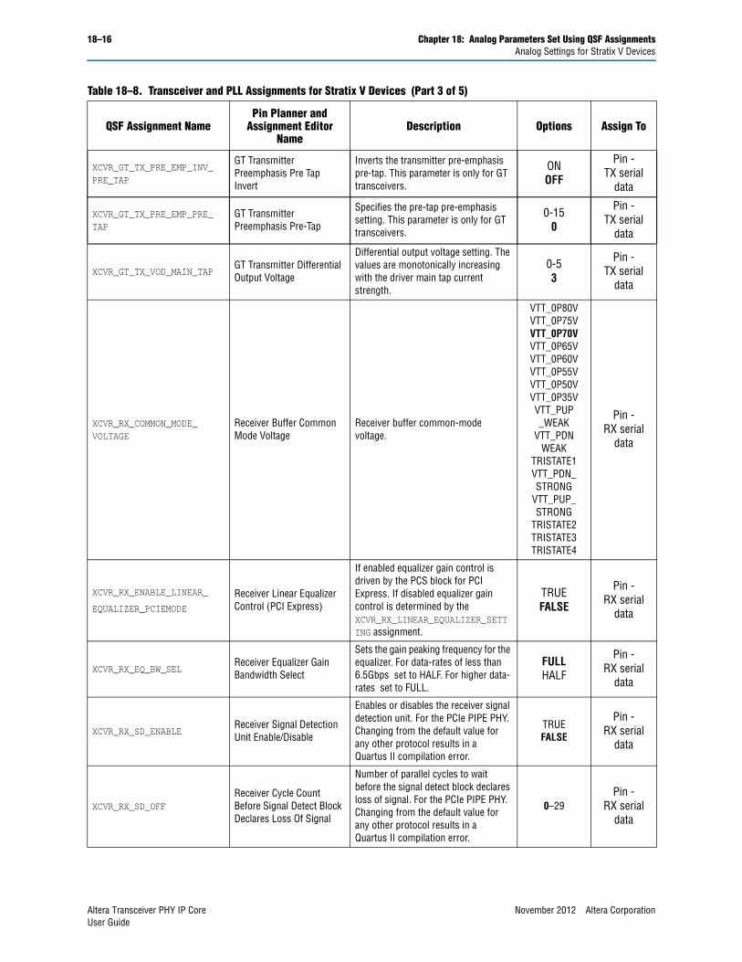
18–16 Chapter 18: Analog Parameters Set Using QSF AssignmentsAnalog Settings for Stratix V Devices
XCVR_GT_TX_PRE_EMP_INV_PRE_TAP
GT Transmitter Preemphasis Pre Tap Invert
Inverts the transmitter pre-emphasis pre-tap. This parameter is only for GT transceivers.
ONOFF
Pin - TX serial
data
XCVR_GT_TX_PRE_EMP_PRE_TAP
GT Transmitter Preemphasis Pre-Tap
Specifies the pre-tap pre-emphasis setting. This parameter is only for GT transceivers.
0-150
Pin - TX serial
data
XCVR_GT_TX_VOD_MAIN_TAPGT Transmitter Differential Output Voltage
Differential output voltage setting. The values are monotonically increasing with the driver main tap current strength.
0-53
Pin - TX serial
data
XCVR_RX_COMMON_MODE_VOLTAGE
Receiver Buffer Common Mode Voltage
Receiver buffer common-mode voltage.
VTT_0P80VVTT_0P75VVTT_0P70VVTT_0P65VVTT_0P60VVTT_0P55VVTT_0P50VVTT_0P35VVTT_PUP_WEAK
VTT_PDNWEAK
TRISTATE1VTT_PDN_STRONG
VTT_PUP_STRONG
TRISTATE2TRISTATE3TRISTATE4
Pin - RX serial
data
XCVR_RX_ENABLE_LINEAR_
EQUALIZER_PCIEMODE
Receiver Linear Equalizer Control (PCI Express)
If enabled equalizer gain control is driven by the PCS block for PCI Express. If disabled equalizer gain control is determined by the XCVR_RX_LINEAR_EQUALIZER_SETTING assignment.
TRUEFALSE
Pin - RX serial
data
XCVR_RX_EQ_BW_SELReceiver Equalizer Gain Bandwidth Select
Sets the gain peaking frequency for the equalizer. For data-rates of less than 6.5Gbps set to HALF. For higher data-rates set to FULL.
FULLHALF
Pin - RX serial
data
XCVR_RX_SD_ENABLEReceiver Signal Detection Unit Enable/Disable
Enables or disables the receiver signal detection unit. For the PCIe PIPE PHY. Changing from the default value for any other protocol results in a Quartus II compilation error.
TRUE FALSE
Pin - RX serial
data
XCVR_RX_SD_OFFReceiver Cycle Count Before Signal Detect Block Declares Loss Of Signal
Number of parallel cycles to wait before the signal detect block declares loss of signal. For the PCIe PIPE PHY. Changing from the default value for any other protocol results in a Quartus II compilation error.
0–29Pin -
RX serial data
Table 18–8. Transceiver and PLL Assignments for Stratix V Devices (Part 3 of 5)
QSF Assignment NamePin Planner and
Assignment Editor Name
Description Options Assign To
Altera Transceiver PHY IP Core November 2012 Altera CorporationUser Guide
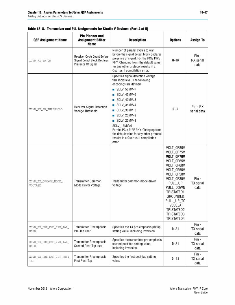
Chapter 18: Analog Parameters Set Using QSF Assignments 18–17Analog Settings for Stratix V Devices
XCVR_RX_SD_ONReceiver Cycle Count Before Signal Detect Block Declares Presence Of Signal
Number of parallel cycles to wait before the signal detect block declares presence of signal. For the PCIe PIPE PHY. Changing from the default value for any other protocol results in a Quartus II compilation error.
0–16Pin -
RX serial data
XCVR_RX_SD_THRESHOLDReceiver Signal Detection Voltage Threshold
Specifies signal detection voltage threshold level. The following encodings are defined:
■ SDLV_50MV=7
■ SDLV_45MV=6
■ SDLV_40MV=5
■ SDLV_35MV=4
■ SDLV_30MV=3
■ SDLV_25MV=2
■ SDLV_20MV=1
SDLV_15MV=0For the PCIe PIPE PHY. Changing from the default value for any other protocol results in a Quartus II compilation error.
0 –7Pin - RX
serial data
XCVR_TX_COMMON_MODE_VOLTAGE
Transmitter Common Mode Driver Voltage
Transmitter common-mode driver voltage
VOLT_0P80VVOLT_0P75VVOLT_0P70VVOLT_0P65VVOLT_0P60VVOLT_0P55VVOLT_0P50VVOLT_0P35V
PULL_UPPULL_DOWNTRISTATED1GROUNDED
PULL_UP_TOVCCELA
TRISTATED2TRISTATED3TRISTATED4
Pin - TX serial
data
XCVR_TX_PRE_EMP_PRE_TAP_USER
Transmitter Preemphasis Pre-Tap user
Specifies the TX pre-emphasis pretap setting value, including inversion. 0–31
Pin -TX serial
data
XCVR_TX_PRE_EMP_2ND_TAP_USER
Transmitter Preemphasis Second Post-Tap user
Specifies the transmitter pre-emphasis second post-tap setting value, including inversion.
0–31Pin -
TX serial data
XCVR_TX_PRE_EMP_1ST_POST_TAP
Transmitter Preemphasis First Post-Tap
Specifies the first post-tap setting value. 0 –31
Pin - TX serial
data
Table 18–8. Transceiver and PLL Assignments for Stratix V Devices (Part 4 of 5)
QSF Assignment NamePin Planner and
Assignment Editor Name
Description Options Assign To
November 2012 Altera Corporation Altera Transceiver PHY IP CoreUser Guide
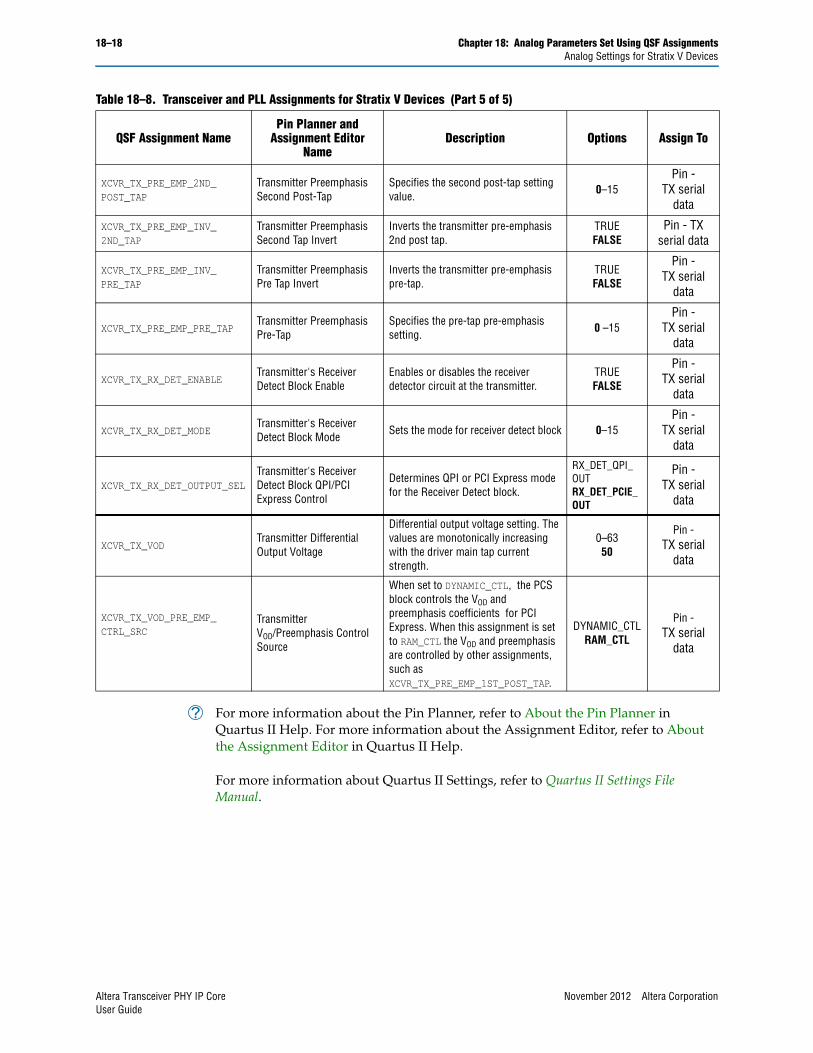
18–18 Chapter 18: Analog Parameters Set Using QSF AssignmentsAnalog Settings for Stratix V Devices
h For more information about the Pin Planner, refer to About the Pin Planner in Quartus II Help. For more information about the Assignment Editor, refer to About the Assignment Editor in Quartus II Help.
For more information about Quartus II Settings, refer to Quartus II Settings File Manual.
XCVR_TX_PRE_EMP_2ND_POST_TAP
Transmitter Preemphasis Second Post-Tap
Specifies the second post-tap setting value. 0–15
Pin - TX serial
data
XCVR_TX_PRE_EMP_INV_2ND_TAP
Transmitter Preemphasis Second Tap Invert
Inverts the transmitter pre-emphasis 2nd post tap.
TRUEFALSE
Pin - TX serial data
XCVR_TX_PRE_EMP_INV_PRE_TAP
Transmitter Preemphasis Pre Tap Invert
Inverts the transmitter pre-emphasis pre-tap.
TRUEFALSE
Pin - TX serial
data
XCVR_TX_PRE_EMP_PRE_TAPTransmitter PreemphasisPre-Tap
Specifies the pre-tap pre-emphasis setting.
0 –15Pin -
TX serial data
XCVR_TX_RX_DET_ENABLETransmitter's Receiver Detect Block Enable
Enables or disables the receiver detector circuit at the transmitter.
TRUEFALSE
Pin - TX serial
data
XCVR_TX_RX_DET_MODETransmitter's Receiver Detect Block Mode
Sets the mode for receiver detect block 0–15Pin -
TX serial data
XCVR_TX_RX_DET_OUTPUT_SELTransmitter's Receiver Detect Block QPI/PCI Express Control
Determines QPI or PCI Express mode for the Receiver Detect block.
RX_DET_QPI_OUT RX_DET_PCIE_OUT
Pin - TX serial
data
XCVR_TX_VODTransmitter Differential Output Voltage
Differential output voltage setting. The values are monotonically increasing with the driver main tap current strength.
0–6350
Pin - TX serial
data
XCVR_TX_VOD_PRE_EMP_CTRL_SRC
Transmitter VOD/Preemphasis Control Source
When set to DYNAMIC_CTL, the PCS block controls the VOD and preemphasis coefficients for PCI Express. When this assignment is set to RAM_CTL the VOD and preemphasis are controlled by other assignments, such as XCVR_TX_PRE_EMP_1ST_POST_TAP.
DYNAMIC_CTLRAM_CTL
Pin - TX serial
data
Table 18–8. Transceiver and PLL Assignments for Stratix V Devices (Part 5 of 5)
QSF Assignment NamePin Planner and
Assignment Editor Name
Description Options Assign To
Altera Transceiver PHY IP Core November 2012 Altera CorporationUser Guide
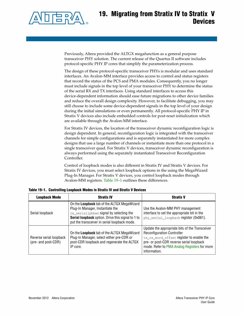
November 2012 Altera Corporation
19. Migrating from Stratix IV to Stratix VDevices
Previously, Altera provided the ALTGX megafunction as a general purpose transceiver PHY solution. The current release of the Quartus II software includes protocol-specific PHY IP cores that simplify the parameterization process.
The design of these protocol-specific transceiver PHYs is modular and uses standard interfaces. An Avalon-MM interface provides access to control and status registers that record the status of the PCS and PMA modules. Consequently, you no longer must include signals in the top level of your transceiver PHY to determine the status of the serial RX and TX interfaces. Using standard interfaces to access this device-dependent information should ease future migrations to other device families and reduce the overall design complexity. However, to facilitate debugging, you may still choose to include some device-dependent signals in the top level of your design during the initial simulations or even permanently. All protocol-specific PHY IP in Stratix V devices also include embedded controls for post-reset initialization which are available through the Avalon-MM interface.
For Stratix IV devices, the location of the transceiver dynamic reconfiguration logic is design dependent. In general, reconfiguration logic is integrated with the transceiver channels for simple configurations and is separately instantiated for more complex designs that use a large number of channels or instantiate more than one protocol in a single transceiver quad. For Stratix V devices, transceiver dynamic reconfiguration is always performed using the separately instantiated Transceiver Reconfiguration Controller.
Control of loopback modes is also different in Stratix IV and Stratix V devices. For Stratix IV devices, you must select loopback options in the using the MegaWizard Plug-In Manager. For Stratix V devices, you control loopback modes through Avalon-MM registers. Table 19–1 outlines these differences.
Table 19–1. Controlling Loopback Modes in Stratix IV and Stratix V Devices
Loopback Mode Stratix IV Stratix V
Serial loopback
On the Loopback tab of the ALTGX MegaWizard Plug-In Manager, Instantiate the rx_seriallpbken signal by selecting the Serial loopback option. Drive this signal to 1 to put the transceiver in serial loopback mode.
Use the Avalon-MM PHY management interface to set the appropriate bit in the phy_serial_loopback register (0x061).
Reverse serial loopback (pre- and post-CDR)
On the Loopback tab of the ALTGX MegaWizard Plug-In Manager, select either pre-CDR or post-CDR loopback and regenerate the ALTGX IP core.
Update the appropriate bits of the Transceiver Reconfiguration Controller tx_rx_word_offset register to enable the pre- or post-CDR reverse serial loopback mode. Refer to PMA Analog Registers for more information.
Altera Transceiver PHY IP CoreUser Guide
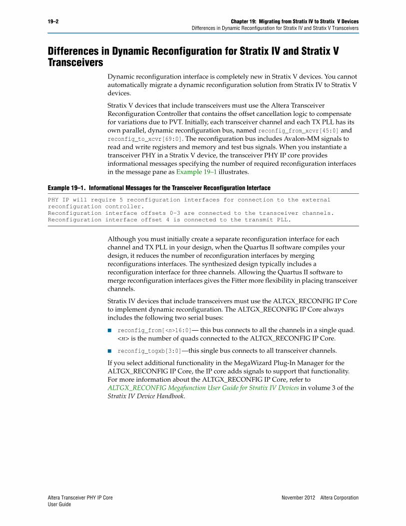
19–2 Chapter 19: Migrating from Stratix IV to Stratix V DevicesDifferences in Dynamic Reconfiguration for Stratix IV and Stratix V Transceivers
Differences in Dynamic Reconfiguration for Stratix IV and Stratix V Transceivers
Dynamic reconfiguration interface is completely new in Stratix V devices. You cannot automatically migrate a dynamic reconfiguration solution from Stratix IV to Stratix V devices.
Stratix V devices that include transceivers must use the Altera Transceiver Reconfiguration Controller that contains the offset cancellation logic to compensate for variations due to PVT. Initially, each transceiver channel and each TX PLL has its own parallel, dynamic reconfiguration bus, named reconfig_from_xcvr[45:0] and reconfig_to_xcvr[69:0]. The reconfiguration bus includes Avalon-MM signals to read and write registers and memory and test bus signals. When you instantiate a transceiver PHY in a Stratix V device, the transceiver PHY IP core provides informational messages specifying the number of required reconfiguration interfaces in the message pane as Example 19–1 illustrates.
Although you must initially create a separate reconfiguration interface for each channel and TX PLL in your design, when the Quartus II software compiles your design, it reduces the number of reconfiguration interfaces by merging reconfigurations interfaces. The synthesized design typically includes a reconfiguration interface for three channels. Allowing the Quartus II software to merge reconfiguration interfaces gives the Fitter more flexibility in placing transceiver channels.
Stratix IV devices that include transceivers must use the ALTGX_RECONFIG IP Core to implement dynamic reconfiguration. The ALTGX_RECONFIG IP Core always includes the following two serial buses:
■ reconfig_from[<n>16:0]— this bus connects to all the channels in a single quad. <n> is the number of quads connected to the ALTGX_RECONFIG IP Core.
■ reconfig_togxb[3:0]—this single bus connects to all transceiver channels.
If you select additional functionality in the MegaWizard Plug-In Manager for the ALTGX_RECONFIG IP Core, the IP core adds signals to support that functionality. For more information about the ALTGX_RECONFIG IP Core, refer to ALTGX_RECONFIG Megafunction User Guide for Stratix IV Devices in volume 3 of the Stratix IV Device Handbook.
Example 19–1. Informational Messages for the Transceiver Reconfiguration Interface
PHY IP will require 5 reconfiguration interfaces for connection to the external reconfiguration controller.Reconfiguration interface offsets 0-3 are connected to the transceiver channels.Reconfiguration interface offset 4 is connected to the transmit PLL.
Altera Transceiver PHY IP Core November 2012 Altera CorporationUser Guide
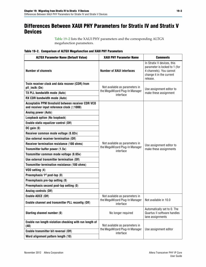
Chapter 19: Migrating from Stratix IV to Stratix V Devices 19–3Differences Between XAUI PHY Parameters for Stratix IV and Stratix V Devices
Differences Between XAUI PHY Parameters for Stratix IV and Stratix V Devices
Table 19–2 lists the XAUI PHY parameters and the corresponding ALTGX megafunction parameters.
Table 19–2. Comparison of ALTGX Megafunction and XAUI PHY Parameters
ALTGX Parameter Name (Default Value) XAUI PHY Parameter Name Comments
Number of channels Number of XAUI interfaces
In Stratix V devices, this parameter is locked to 1 (for 4 channels). You cannot change it in the current release.
Train receiver clock and data recover (CDR) from pll_inclk (On) Not available as parameters in
the MegaWizard Plug-In Manager interface
Use assignment editor to make these assignmentTX PLL bandwidth mode (Auto)
RX CDR bandwidth mode (Auto)
Acceptable PPM threshold between receiver CDR VCO and receiver input reference clock (1000)
Not available as parameters in the MegaWizard Plug-In Manager
interface
Use assignment editor to make these assignments
Analog power (Auto)
Loopback option (No loopback)
Enable static equalizer control (Off)
DC gain (0)
Receiver common mode voltage (0.82v)
Use external receiver termination (Off)
Receiver termination resistance (100 ohms)
Transmitter buffer power (1.5v)
Transmitter common mode voltage (0.65v)
Use external transmitter termination (Off)
Transmitter termination resistance (100 ohms)
VOD setting (4)
Preemphasis 1st post-tap (0)
Preemphasis pre-tap setting (0)
Preemphasis second post-tap setting (0)
Analog controls (Off)
Enable ADCE (Off) Not available as parameters in the MegaWizard Plug-In Manager
interfaceNot available in 10.0
Enable channel and transmitter PLL reconfig (Off)
Starting channel number (0) No longer requiredAutomatically set to 0. The Quartus II software handles lane assignments
Enable run length violation checking with run length of (40) Not available as parameters in
the MegaWizard Plug-In Manager interface
Use assignment editorEnable transmitter bit reversal (Off)
Word alignment pattern length (10)
November 2012 Altera Corporation Altera Transceiver PHY IP CoreUser Guide
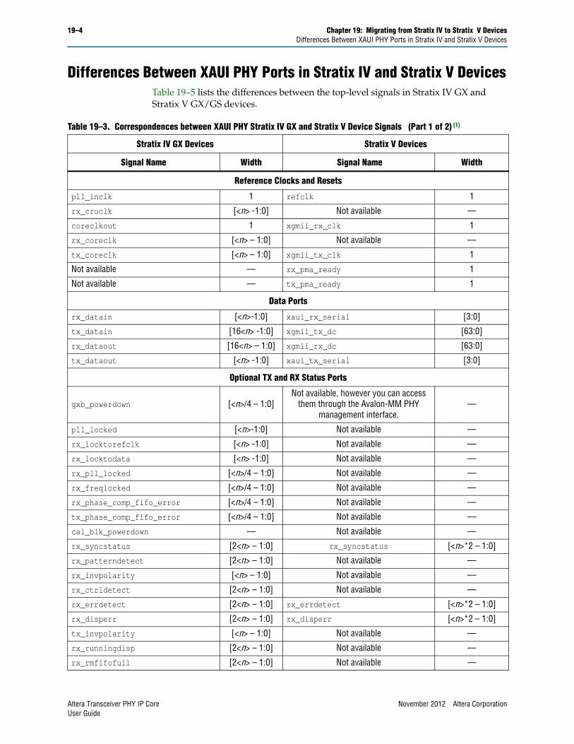
19–4 Chapter 19: Migrating from Stratix IV to Stratix V DevicesDifferences Between XAUI PHY Ports in Stratix IV and Stratix V Devices
Differences Between XAUI PHY Ports in Stratix IV and Stratix V DevicesTable 19–5 lists the differences between the top-level signals in Stratix IV GX and Stratix V GX/GS devices.
Table 19–3. Correspondences between XAUI PHY Stratix IV GX and Stratix V Device Signals (Part 1 of 2) (1)
Stratix IV GX Devices Stratix V Devices
Signal Name Width Signal Name Width
Reference Clocks and Resets
pll_inclk 1 refclk 1
rx_cruclk [<n> -1:0] Not available —
coreclkout 1 xgmii_rx_clk 1
rx_coreclk [<n> – 1:0] Not available —
tx_coreclk [<n> – 1:0] xgmii_tx_clk 1
Not available — rx_pma_ready 1
Not available — tx_pma_ready 1
Data Ports
rx_datain [<n>-1:0] xaui_rx_serial [3:0]
tx_datain [16<n> -1:0] xgmii_tx_dc [63:0]
rx_dataout [16<n> – 1:0] xgmii_rx_dc [63:0]
tx_dataout [<n> -1:0] xaui_tx_serial [3:0]
Optional TX and RX Status Ports
gxb_powerdown [<n>/4 – 1:0]Not available, however you can access
them through the Avalon-MM PHY management interface.
—
pll_locked [<n>-1:0] Not available —
rx_locktorefclk [<n> -1:0] Not available —
rx_locktodata [<n> -1:0] Not available —
rx_pll_locked [<n>/4 – 1:0] Not available —
rx_freqlocked [<n>/4 – 1:0] Not available —
rx_phase_comp_fifo_error [<n>/4 – 1:0] Not available —
tx_phase_comp_fifo_error [<n>/4 – 1:0] Not available —
cal_blk_powerdown — Not available —
rx_syncstatus [2<n> – 1:0] rx_syncstatus [<n>*2 – 1:0]
rx_patterndetect [2<n> – 1:0] Not available —
rx_invpolarity [<n> – 1:0] Not available —
rx_ctrldetect [2<n> – 1:0] Not available —
rx_errdetect [2<n> – 1:0] rx_errdetect [<n>*2 – 1:0]
rx_disperr [2<n> – 1:0] rx_disperr [<n>*2 – 1:0]
tx_invpolarity [<n> – 1:0] Not available —
rx_runningdisp [2<n> – 1:0] Not available —
rx_rmfifofull [2<n> – 1:0] Not available —
Altera Transceiver PHY IP Core November 2012 Altera CorporationUser Guide
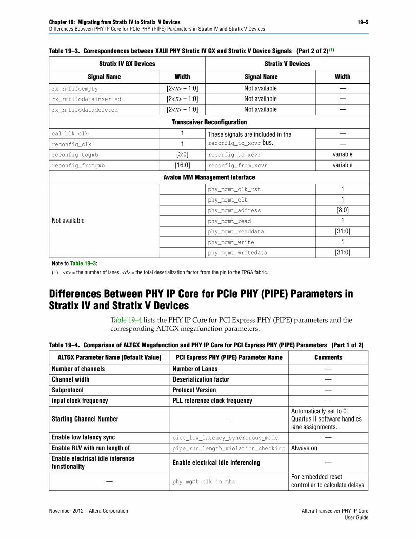
Chapter 19: Migrating from Stratix IV to Stratix V Devices 19–5Differences Between PHY IP Core for PCIe PHY (PIPE) Parameters in Stratix IV and Stratix V Devices
Differences Between PHY IP Core for PCIe PHY (PIPE) Parameters in Stratix IV and Stratix V Devices
Table 19–4 lists the PHY IP Core for PCI Express PHY (PIPE) parameters and the corresponding ALTGX megafunction parameters.
rx_rmfifoempty [2<n> – 1:0] Not available —
rx_rmfifodatainserted [2<n> – 1:0] Not available —
rx_rmfifodatadeleted [2<n> – 1:0] Not available —
Transceiver Reconfiguration
cal_blk_clk 1 These signals are included in the reconfig_to_xcvr bus.
—
reconfig_clk 1 —
reconfig_togxb [3:0] reconfig_to_xcvr variable
reconfig_fromgxb [16:0] reconfig_from_xcvr variable
Avalon MM Management Interface
Not available
phy_mgmt_clk_rst 1
phy_mgmt_clk 1
phy_mgmt_address [8:0]
phy_mgmt_read 1
phy_mgmt_readdata [31:0]
phy_mgmt_write 1
phy_mgmt_writedata [31:0]
Note to Table 19–3:
(1) <n> = the number of lanes. <d> = the total deserialization factor from the pin to the FPGA fabric.
Table 19–3. Correspondences between XAUI PHY Stratix IV GX and Stratix V Device Signals (Part 2 of 2) (1)
Stratix IV GX Devices Stratix V Devices
Signal Name Width Signal Name Width
Table 19–4. Comparison of ALTGX Megafunction and PHY IP Core for PCI Express PHY (PIPE) Parameters (Part 1 of 2)
ALTGX Parameter Name (Default Value) PCI Express PHY (PIPE) Parameter Name Comments
Number of channels Number of Lanes —
Channel width Deserialization factor —
Subprotocol Protocol Version —
input clock frequency PLL reference clock frequency —
Starting Channel Number —Automatically set to 0. Quartus II software handles lane assignments.
Enable low latency sync pipe_low_latency_syncronous_mode —
Enable RLV with run length of pipe_run_length_violation_checking Always on
Enable electrical idle inference functionality Enable electrical idle inferencing —
— phy_mgmt_clk_in_mhzFor embedded reset controller to calculate delays
November 2012 Altera Corporation Altera Transceiver PHY IP CoreUser Guide
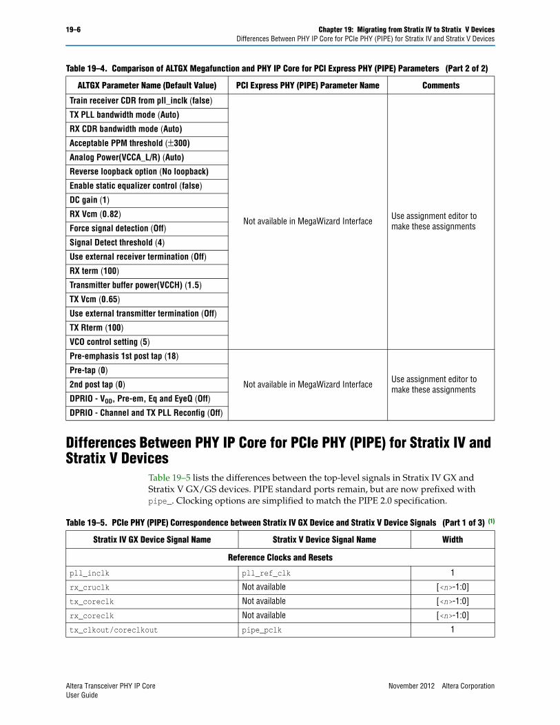
19–6 Chapter 19: Migrating from Stratix IV to Stratix V DevicesDifferences Between PHY IP Core for PCIe PHY (PIPE) for Stratix IV and Stratix V Devices
Differences Between PHY IP Core for PCIe PHY (PIPE) for Stratix IV and Stratix V Devices
Table 19–5 lists the differences between the top-level signals in Stratix IV GX and Stratix V GX/GS devices. PIPE standard ports remain, but are now prefixed with pipe_. Clocking options are simplified to match the PIPE 2.0 specification.
Train receiver CDR from pll_inclk (false)
Not available in MegaWizard Interface Use assignment editor to make these assignments
TX PLL bandwidth mode (Auto)
RX CDR bandwidth mode (Auto)
Acceptable PPM threshold (300)
Analog Power(VCCA_L/R) (Auto)
Reverse loopback option (No loopback)
Enable static equalizer control (false)
DC gain (1)
RX Vcm (0.82)
Force signal detection (Off)
Signal Detect threshold (4)
Use external receiver termination (Off)
RX term (100)
Transmitter buffer power(VCCH) (1.5)
TX Vcm (0.65)
Use external transmitter termination (Off)
TX Rterm (100)
VCO control setting (5)
Pre-emphasis 1st post tap (18)
Not available in MegaWizard Interface Use assignment editor to make these assignments
Pre-tap (0)
2nd post tap (0)
DPRIO - VOD, Pre-em, Eq and EyeQ (Off)
DPRIO - Channel and TX PLL Reconfig (Off)
Table 19–4. Comparison of ALTGX Megafunction and PHY IP Core for PCI Express PHY (PIPE) Parameters (Part 2 of 2)
ALTGX Parameter Name (Default Value) PCI Express PHY (PIPE) Parameter Name Comments
Table 19–5. PCIe PHY (PIPE) Correspondence between Stratix IV GX Device and Stratix V Device Signals (Part 1 of 3) (1)
Stratix IV GX Device Signal Name Stratix V Device Signal Name Width
Reference Clocks and Resets
pll_inclk pll_ref_clk 1
rx_cruclk Not available [<n>-1:0]
tx_coreclk Not available [<n>-1:0]
rx_coreclk Not available [<n>-1:0]
tx_clkout/coreclkout pipe_pclk 1
Altera Transceiver PHY IP Core November 2012 Altera CorporationUser Guide
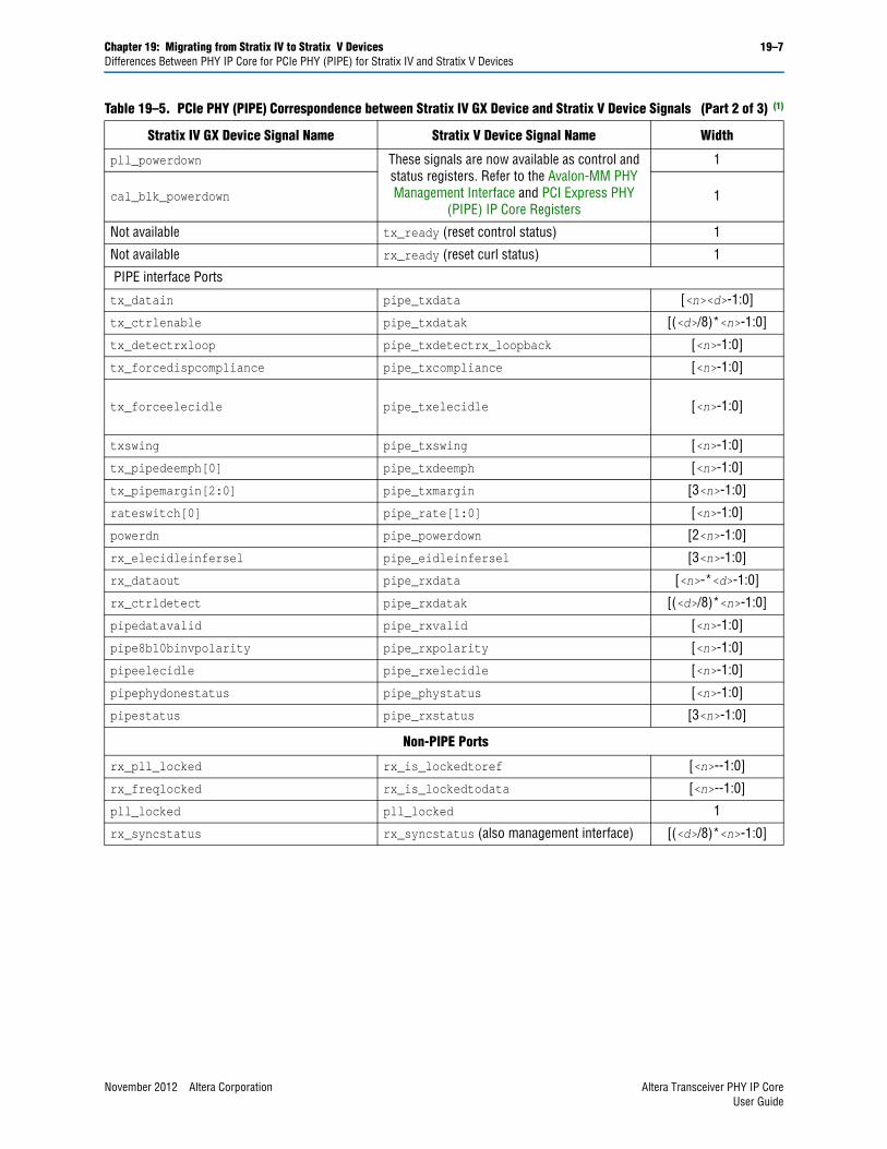
Chapter 19: Migrating from Stratix IV to Stratix V Devices 19–7Differences Between PHY IP Core for PCIe PHY (PIPE) for Stratix IV and Stratix V Devices
pll_powerdown These signals are now available as control and status registers. Refer to the Avalon-MM PHY Management Interface and PCI Express PHY
(PIPE) IP Core Registers
1
cal_blk_powerdown 1
Not available tx_ready (reset control status) 1
Not available rx_ready (reset curl status) 1
PIPE interface Ports
tx_datain pipe_txdata [<n><d>-1:0]
tx_ctrlenable pipe_txdatak [(<d>/8)*<n>-1:0]
tx_detectrxloop pipe_txdetectrx_loopback [<n>-1:0]
tx_forcedispcompliance pipe_txcompliance [<n>-1:0]
tx_forceelecidle pipe_txelecidle [<n>-1:0]
txswing pipe_txswing [<n>-1:0]
tx_pipedeemph[0] pipe_txdeemph [<n>-1:0]
tx_pipemargin[2:0] pipe_txmargin [3<n>-1:0]
rateswitch[0] pipe_rate[1:0] [<n>-1:0]
powerdn pipe_powerdown [2<n>-1:0]
rx_elecidleinfersel pipe_eidleinfersel [3<n>-1:0]
rx_dataout pipe_rxdata [<n>-*<d>-1:0]
rx_ctrldetect pipe_rxdatak [(<d>/8)*<n>-1:0]
pipedatavalid pipe_rxvalid [<n>-1:0]
pipe8b10binvpolarity pipe_rxpolarity [<n>-1:0]
pipeelecidle pipe_rxelecidle [<n>-1:0]
pipephydonestatus pipe_phystatus [<n>-1:0]
pipestatus pipe_rxstatus [3<n>-1:0]
Non-PIPE Ports
rx_pll_locked rx_is_lockedtoref [<n>--1:0]
rx_freqlocked rx_is_lockedtodata [<n>--1:0]
pll_locked pll_locked 1
rx_syncstatus rx_syncstatus (also management interface) [(<d>/8)*<n>-1:0]
Table 19–5. PCIe PHY (PIPE) Correspondence between Stratix IV GX Device and Stratix V Device Signals (Part 2 of 3) (1)
Stratix IV GX Device Signal Name Stratix V Device Signal Name Width
November 2012 Altera Corporation Altera Transceiver PHY IP CoreUser Guide
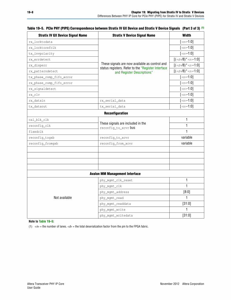
19–8 Chapter 19: Migrating from Stratix IV to Stratix V DevicesDifferences Between PHY IP Core for PCIe PHY (PIPE) for Stratix IV and Stratix V Devices
rx_locktodata
These signals are now available as control and status registers. Refer to the “Register Interface
and Register Descriptions”
[<n>-1:0]
rx_locktorefclk [<n>-1:0]
tx_invpolarity [<n>-1:0]
rx_errdetect [(<d>/8)*<n>-1:0]
rx_disperr [(<d>/8)*<n>-1:0]
rx_patterndetect [(<d>/8)*<n>-1:0]
tx_phase_comp_fifo_error [<n>-1:0]
rx_phase_comp_fifo_error [<n>-1:0]
rx_signaldetect [<n>-1:0]
rx_rlv [<n>-1:0]
rx_datain rx_serial_data [<n>-1:0]
tx_dataout tx_serial_data [<n>-1:0]
Reconfiguration
cal_blk_clkThese signals are included in the reconfig_to_xcvr bus
1
reconfig_clk 1
fixedclk 1
reconfig_togxb reconfig_to_xcvr variable
reconfig_fromgxb reconfig_from_xcvr variable
Avalon MM Management Interface
Not available
phy_mgmt_clk_reset 1
phy_mgmt_clk 1
phy_mgmt_address [8:0]
phy_mgmt_read 1
phy_mgmt_readdata [31:0]
phy_mgmt_write 1
phy_mgmt_writedata [31:0]
Note to Table 19–5:
(1) <n> = the number of lanes. <d> = the total deserialization factor from the pin to the FPGA fabric.
Table 19–5. PCIe PHY (PIPE) Correspondence between Stratix IV GX Device and Stratix V Device Signals (Part 3 of 3) (1)
Stratix IV GX Device Signal Name Stratix V Device Signal Name Width
Altera Transceiver PHY IP Core November 2012 Altera CorporationUser Guide
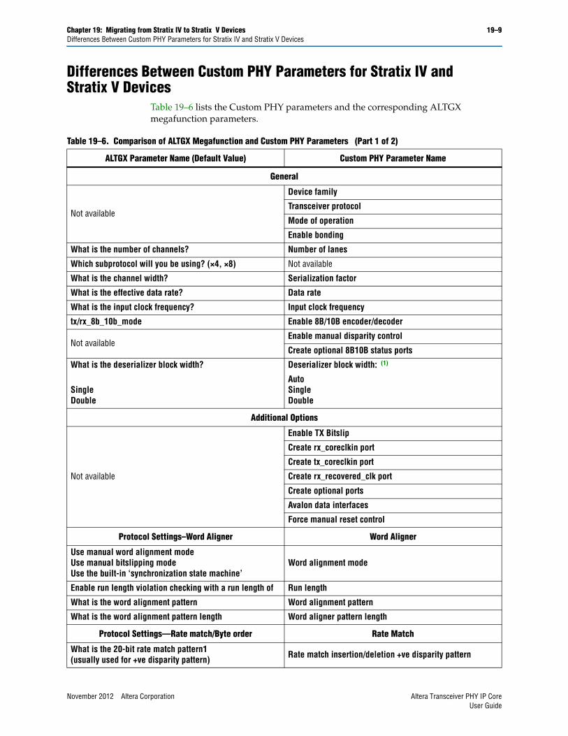
Chapter 19: Migrating from Stratix IV to Stratix V Devices 19–9Differences Between Custom PHY Parameters for Stratix IV and Stratix V Devices
Differences Between Custom PHY Parameters for Stratix IV and Stratix V Devices
Table 19–6 lists the Custom PHY parameters and the corresponding ALTGX megafunction parameters.
Table 19–6. Comparison of ALTGX Megafunction and Custom PHY Parameters (Part 1 of 2)
ALTGX Parameter Name (Default Value) Custom PHY Parameter Name
General
Not available
Device family
Transceiver protocol
Mode of operation
Enable bonding
What is the number of channels? Number of lanes
Which subprotocol will you be using? (×4, ×8) Not available
What is the channel width? Serialization factor
What is the effective data rate? Data rate
What is the input clock frequency? Input clock frequency
tx/rx_8b_10b_mode Enable 8B/10B encoder/decoder
Not availableEnable manual disparity control
Create optional 8B10B status ports
What is the deserializer block width?
Single Double
Deserializer block width: (1)
AutoSingleDouble
Additional Options
Not available
Enable TX Bitslip
Create rx_coreclkin port
Create tx_coreclkin port
Create rx_recovered_clk port
Create optional ports
Avalon data interfaces
Force manual reset control
Protocol Settings–Word Aligner Word Aligner
Use manual word alignment modeUse manual bitslipping modeUse the built-in ‘synchronization state machine’
Word alignment mode
Enable run length violation checking with a run length of Run length
What is the word alignment pattern Word alignment pattern
What is the word alignment pattern length Word aligner pattern length
Protocol Settings—Rate match/Byte order Rate Match
What is the 20-bit rate match pattern1 (usually used for +ve disparity pattern) Rate match insertion/deletion +ve disparity pattern
November 2012 Altera Corporation Altera Transceiver PHY IP CoreUser Guide
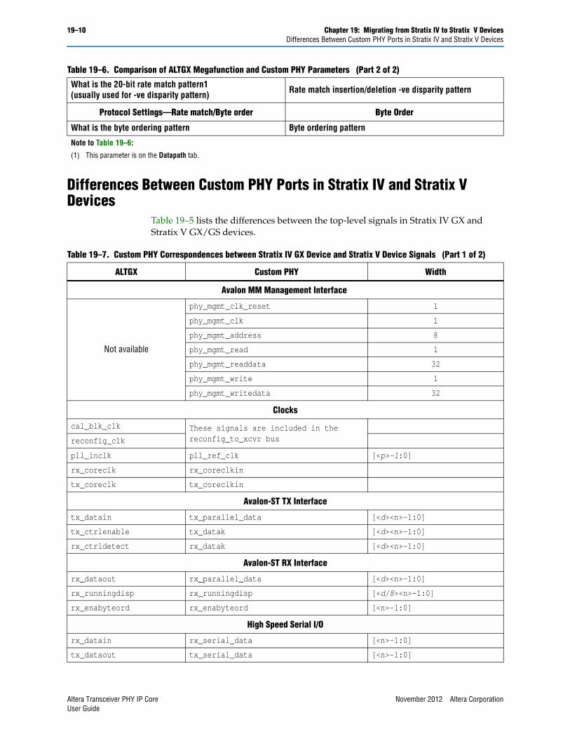
19–10 Chapter 19: Migrating from Stratix IV to Stratix V DevicesDifferences Between Custom PHY Ports in Stratix IV and Stratix V Devices
Differences Between Custom PHY Ports in Stratix IV and Stratix V Devices
Table 19–5 lists the differences between the top-level signals in Stratix IV GX and Stratix V GX/GS devices.
What is the 20-bit rate match pattern1 (usually used for -ve disparity pattern) Rate match insertion/deletion -ve disparity pattern
Protocol Settings—Rate match/Byte order Byte Order
What is the byte ordering pattern Byte ordering pattern
Note to Table 19–6:
(1) This parameter is on the Datapath tab.
Table 19–6. Comparison of ALTGX Megafunction and Custom PHY Parameters (Part 2 of 2)
Table 19–7. Custom PHY Correspondences between Stratix IV GX Device and Stratix V Device Signals (Part 1 of 2)
ALTGX Custom PHY Width
Avalon MM Management Interface
Not available
phy_mgmt_clk_reset 1
phy_mgmt_clk 1
phy_mgmt_address 8
phy_mgmt_read 1
phy_mgmt_readdata 32
phy_mgmt_write 1
phy_mgmt_writedata 32
Clocks
cal_blk_clk These signals are included in the reconfig_to_xcvr busreconfig_clk
pll_inclk pll_ref_clk [<p>-1:0]
rx_coreclk rx_coreclkin
tx_coreclk tx_coreclkin
Avalon-ST TX Interface
tx_datain tx_parallel_data [<d><n>-1:0]
tx_ctrlenable tx_datak [<d><n>-1:0]
rx_ctrldetect rx_datak [<d><n>-1:0]
Avalon-ST RX Interface
rx_dataout rx_parallel_data [<d><n>-1:0]
rx_runningdisp rx_runningdisp [<d/8><n>-1:0]
rx_enabyteord rx_enabyteord [<n>-1:0]
High Speed Serial I/O
rx_datain rx_serial_data [<n>-1:0]
tx_dataout tx_serial_data [<n>-1:0]
Altera Transceiver PHY IP Core November 2012 Altera CorporationUser Guide
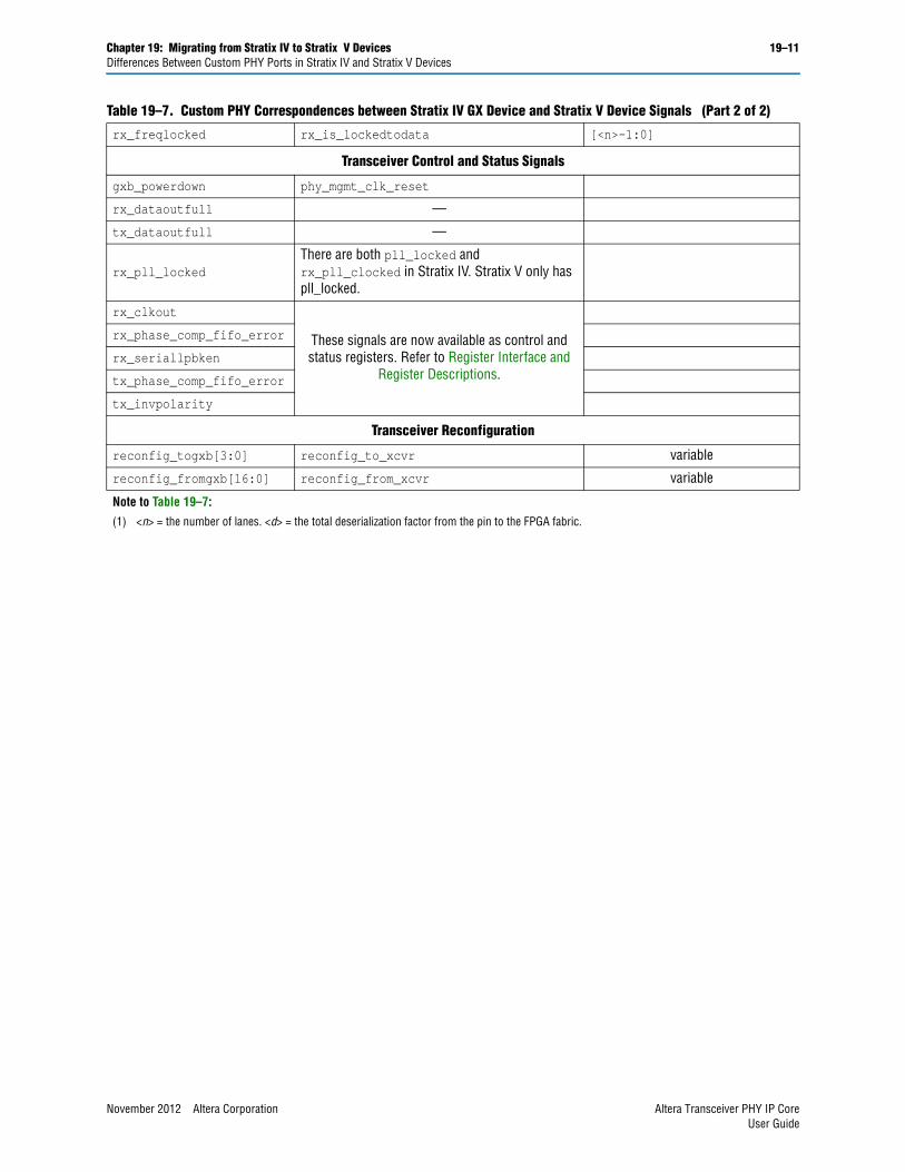
Chapter 19: Migrating from Stratix IV to Stratix V Devices 19–11Differences Between Custom PHY Ports in Stratix IV and Stratix V Devices
rx_freqlocked rx_is_lockedtodata [<n>-1:0]
Transceiver Control and Status Signals
gxb_powerdown phy_mgmt_clk_reset
rx_dataoutfull —
tx_dataoutfull —
rx_pll_lockedThere are both pll_locked and rx_pll_clocked in Stratix IV. Stratix V only has pll_locked.
rx_clkout
These signals are now available as control and status registers. Refer to Register Interface and
Register Descriptions.
rx_phase_comp_fifo_error
rx_seriallpbken
tx_phase_comp_fifo_error
tx_invpolarity
Transceiver Reconfiguration
reconfig_togxb[3:0] reconfig_to_xcvr variable
reconfig_fromgxb[16:0] reconfig_from_xcvr variable
Note to Table 19–7:
(1) <n> = the number of lanes. <d> = the total deserialization factor from the pin to the FPGA fabric.
Table 19–7. Custom PHY Correspondences between Stratix IV GX Device and Stratix V Device Signals (Part 2 of 2)
November 2012 Altera Corporation Altera Transceiver PHY IP CoreUser Guide

19–12 Chapter 19: Migrating from Stratix IV to Stratix V DevicesDifferences Between Custom PHY Ports in Stratix IV and Stratix V Devices
Altera Transceiver PHY IP Core November 2012 Altera CorporationUser Guide
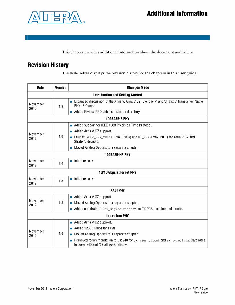
November 2012 Altera Corporation
Additional Information
This chapter provides additional information about the document and Altera.
Revision HistoryThe table below displays the revision history for the chapters in this user guide.
Date Version Changes Made
Introduction and Getting Started
November 2012 1.8
■ Expanded discussion of the Arria V, Arria V GZ, Cyclone V, and Stratix V Transceiver Native PHY IP Cores.
■ Added Riviera-PRO aldec simulation directory.
10GBASE-R PHY
November 2012 1.8
■ Added support for IEEE 1588 Precision Time Protocol.
■ Added Arria V GZ support.
■ Enabled RCLR_BER_COUNT (0x81, bit 3) and HI_BER (0x82, bit 1) for Arria V GZ and Stratix V devices.
■ Moved Analog Options to a separate chapter.
10GBASE-KR PHY
November 2012 1.8 ■ Initial release.
1G/10 Gbps Ethernet PHY
November 2012 1.8 ■ Initial release.
XAUI PHY
November 2012 1.8
■ Added Arria V GZ support.
■ Moved Analog Options to a separate chapter.
■ Added constraint for tx_digitalreset when TX PCS uses bonded clocks.
Interlaken PHY
November 2012 1.8
■ Added Arria V GZ support.
■ Added 12500 Mbps lane rate.
■ Moved Analog Options to a separate chapter.
■ Removed recommendation to use /40 for tx_user_clkout and rx_coreclkin. Data rates between /40 and /67 all work reliably.
Altera Transceiver PHY IP CoreUser Guide
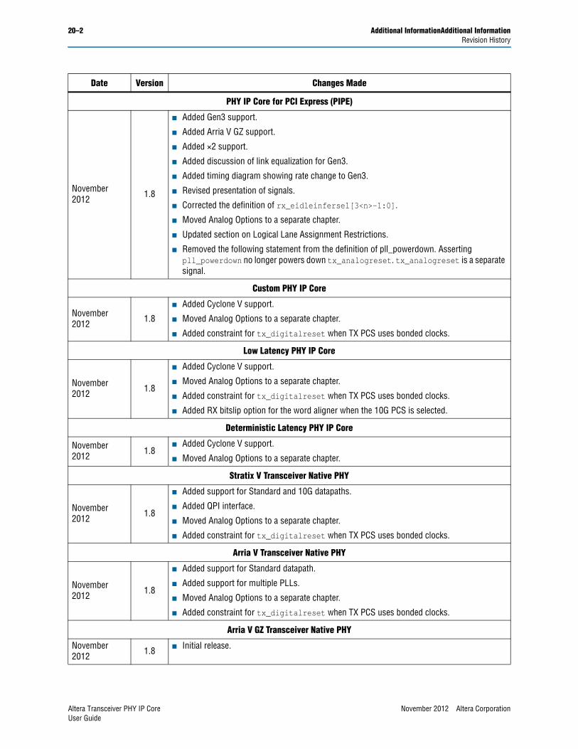
20–2 Additional InformationAdditional InformationRevision History
PHY IP Core for PCI Express (PIPE)
November 2012 1.8
■ Added Gen3 support.
■ Added Arria V GZ support.
■ Added ×2 support.
■ Added discussion of link equalization for Gen3.
■ Added timing diagram showing rate change to Gen3.
■ Revised presentation of signals.
■ Corrected the definition of rx_eidleinfersel[3<n>-1:0].
■ Moved Analog Options to a separate chapter.
■ Updated section on Logical Lane Assignment Restrictions.
■ Removed the following statement from the definition of pll_powerdown. Asserting pll_powerdown no longer powers down tx_analogreset. tx_analogreset is a separate signal.
Custom PHY IP Core
November 2012 1.8
■ Added Cyclone V support.
■ Moved Analog Options to a separate chapter.
■ Added constraint for tx_digitalreset when TX PCS uses bonded clocks.
Low Latency PHY IP Core
November 2012 1.8
■ Added Cyclone V support.
■ Moved Analog Options to a separate chapter.
■ Added constraint for tx_digitalreset when TX PCS uses bonded clocks.
■ Added RX bitslip option for the word aligner when the 10G PCS is selected.
Deterministic Latency PHY IP Core
November 2012 1.8
■ Added Cyclone V support.
■ Moved Analog Options to a separate chapter.
Stratix V Transceiver Native PHY
November 2012 1.8
■ Added support for Standard and 10G datapaths.
■ Added QPI interface.
■ Moved Analog Options to a separate chapter.
■ Added constraint for tx_digitalreset when TX PCS uses bonded clocks.
Arria V Transceiver Native PHY
November 2012 1.8
■ Added support for Standard datapath.
■ Added support for multiple PLLs.
■ Moved Analog Options to a separate chapter.
■ Added constraint for tx_digitalreset when TX PCS uses bonded clocks.
Arria V GZ Transceiver Native PHY
November 2012 1.8 ■ Initial release.
Date Version Changes Made
Altera Transceiver PHY IP Core November 2012 Altera CorporationUser Guide
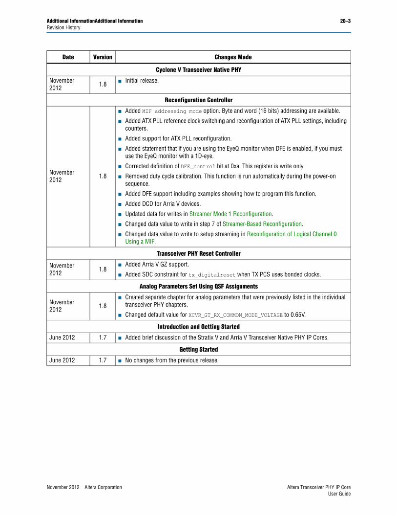
Additional InformationAdditional Information 20–3Revision History
Cyclone V Transceiver Native PHY
November 2012 1.8 ■ Initial release.
Reconfiguration Controller
November 2012 1.8
■ Added MIF addressing mode option. Byte and word (16 bits) addressing are available.
■ Added ATX PLL reference clock switching and reconfiguration of ATX PLL settings, including counters.
■ Added support for ATX PLL reconfiguration.
■ Added statement that if you are using the EyeQ monitor when DFE is enabled, if you must use the EyeQ monitor with a 1D-eye.
■ Corrected definition of DFE_control bit at 0xa. This register is write only.
■ Removed duty cycle calibration. This function is run automatically during the power-on sequence.
■ Added DFE support including examples showing how to program this function.
■ Added DCD for Arria V devices.
■ Updated data for writes in Streamer Mode 1 Reconfiguration.
■ Changed data value to write in step 7 of Streamer-Based Reconfiguration.
■ Changed data value to write to setup streaming in Reconfiguration of Logical Channel 0 Using a MIF.
Transceiver PHY Reset Controller
November 2012 1.8
■ Added Arria V GZ support.
■ Added SDC constraint for tx_digitalreset when TX PCS uses bonded clocks.
Analog Parameters Set Using QSF Assignments
November 2012 1.8
■ Created separate chapter for analog parameters that were previously listed in the individual transceiver PHY chapters.
■ Changed default value for XCVR_GT_RX_COMMON_MODE_VOLTAGE to 0.65V.
Introduction and Getting Started
June 2012 1.7 ■ Added brief discussion of the Stratix V and Arria V Transceiver Native PHY IP Cores.
Getting Started
June 2012 1.7 ■ No changes from the previous release.
Date Version Changes Made
November 2012 Altera Corporation Altera Transceiver PHY IP CoreUser Guide
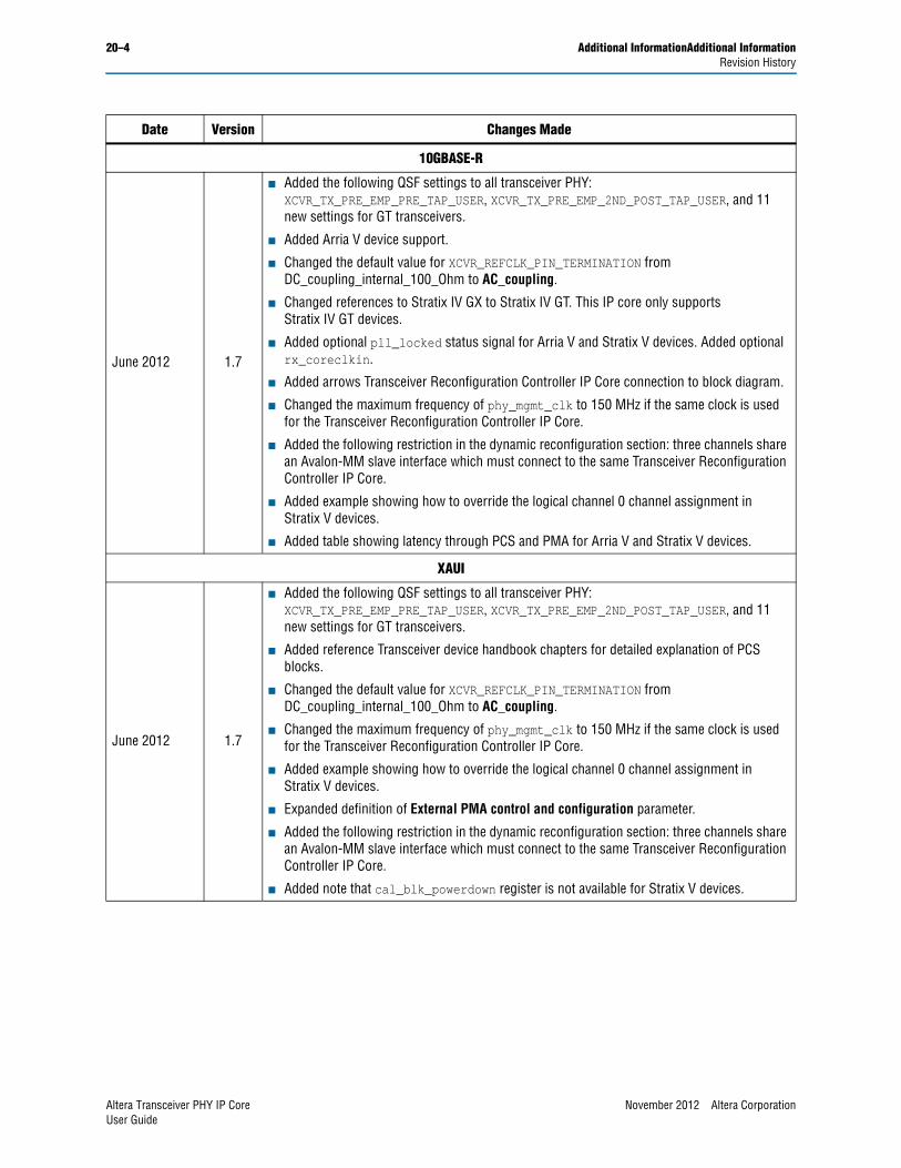
20–4 Additional InformationAdditional InformationRevision History
10GBASE-R
June 2012 1.7
■ Added the following QSF settings to all transceiver PHY: XCVR_TX_PRE_EMP_PRE_TAP_USER, XCVR_TX_PRE_EMP_2ND_POST_TAP_USER, and 11 new settings for GT transceivers.
■ Added Arria V device support.
■ Changed the default value for XCVR_REFCLK_PIN_TERMINATION from DC_coupling_internal_100_Ohm to AC_coupling.
■ Changed references to Stratix IV GX to Stratix IV GT. This IP core only supports Stratix IV GT devices.
■ Added optional pll_locked status signal for Arria V and Stratix V devices. Added optional rx_coreclkin.
■ Added arrows Transceiver Reconfiguration Controller IP Core connection to block diagram.
■ Changed the maximum frequency of phy_mgmt_clk to 150 MHz if the same clock is used for the Transceiver Reconfiguration Controller IP Core.
■ Added the following restriction in the dynamic reconfiguration section: three channels share an Avalon-MM slave interface which must connect to the same Transceiver Reconfiguration Controller IP Core.
■ Added example showing how to override the logical channel 0 channel assignment in Stratix V devices.
■ Added table showing latency through PCS and PMA for Arria V and Stratix V devices.
XAUI
June 2012 1.7
■ Added the following QSF settings to all transceiver PHY: XCVR_TX_PRE_EMP_PRE_TAP_USER, XCVR_TX_PRE_EMP_2ND_POST_TAP_USER, and 11 new settings for GT transceivers.
■ Added reference Transceiver device handbook chapters for detailed explanation of PCS blocks.
■ Changed the default value for XCVR_REFCLK_PIN_TERMINATION from DC_coupling_internal_100_Ohm to AC_coupling.
■ Changed the maximum frequency of phy_mgmt_clk to 150 MHz if the same clock is used for the Transceiver Reconfiguration Controller IP Core.
■ Added example showing how to override the logical channel 0 channel assignment in Stratix V devices.
■ Expanded definition of External PMA control and configuration parameter.
■ Added the following restriction in the dynamic reconfiguration section: three channels share an Avalon-MM slave interface which must connect to the same Transceiver Reconfiguration Controller IP Core.
■ Added note that cal_blk_powerdown register is not available for Stratix V devices.
Date Version Changes Made
Altera Transceiver PHY IP Core November 2012 Altera CorporationUser Guide
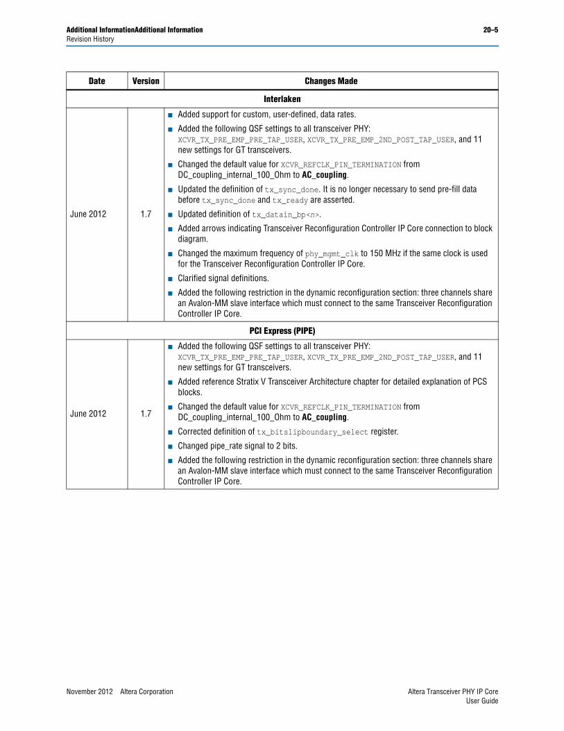
Additional InformationAdditional Information 20–5Revision History
Interlaken
June 2012 1.7
■ Added support for custom, user-defined, data rates.
■ Added the following QSF settings to all transceiver PHY: XCVR_TX_PRE_EMP_PRE_TAP_USER, XCVR_TX_PRE_EMP_2ND_POST_TAP_USER, and 11 new settings for GT transceivers.
■ Changed the default value for XCVR_REFCLK_PIN_TERMINATION from DC_coupling_internal_100_Ohm to AC_coupling.
■ Updated the definition of tx_sync_done. It is no longer necessary to send pre-fill data before tx_sync_done and tx_ready are asserted.
■ Updated definition of tx_datain_bp<n>.
■ Added arrows indicating Transceiver Reconfiguration Controller IP Core connection to block diagram.
■ Changed the maximum frequency of phy_mgmt_clk to 150 MHz if the same clock is used for the Transceiver Reconfiguration Controller IP Core.
■ Clarified signal definitions.
■ Added the following restriction in the dynamic reconfiguration section: three channels share an Avalon-MM slave interface which must connect to the same Transceiver Reconfiguration Controller IP Core.
PCI Express (PIPE)
June 2012 1.7
■ Added the following QSF settings to all transceiver PHY: XCVR_TX_PRE_EMP_PRE_TAP_USER, XCVR_TX_PRE_EMP_2ND_POST_TAP_USER, and 11 new settings for GT transceivers.
■ Added reference Stratix V Transceiver Architecture chapter for detailed explanation of PCS blocks.
■ Changed the default value for XCVR_REFCLK_PIN_TERMINATION from DC_coupling_internal_100_Ohm to AC_coupling.
■ Corrected definition of tx_bitslipboundary_select register.
■ Changed pipe_rate signal to 2 bits.
■ Added the following restriction in the dynamic reconfiguration section: three channels share an Avalon-MM slave interface which must connect to the same Transceiver Reconfiguration Controller IP Core.
Date Version Changes Made
November 2012 Altera Corporation Altera Transceiver PHY IP CoreUser Guide
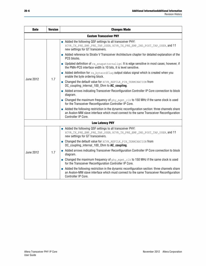
20–6 Additional InformationAdditional InformationRevision History
Custom Transceiver PHY
June 2012 1.7
■ Added the following QSF settings to all transceiver PHY: XCVR_TX_PRE_EMP_PRE_TAP_USER, XCVR_TX_PRE_EMP_2ND_POST_TAP_USER, and 11 new settings for GT transceivers.
■ Added reference to Stratix V Transceiver Architecture chapter for detailed explanation of the PCS blocks.
■ Updated definition of rx_enapatternalign: It is edge sensitive in most cases; however, if the PMA-PCS interface width is 10 bits, it is level sensitive.
■ Added definition for rx_byteordflag output status signal which is created when you enable the byte ordering block.
■ Changed the default value for XCVR_REFCLK_PIN_TERMINATION from DC_coupling_internal_100_Ohm to AC_coupling.
■ Added arrows indicating Transceiver Reconfiguration Controller IP Core connection to block diagram.
■ Changed the maximum frequency of phy_mgmt_clk to 150 MHz if the same clock is used for the Transceiver Reconfiguration Controller IP Core.
■ Added the following restriction in the dynamic reconfiguration section: three channels share an Avalon-MM slave interface which must connect to the same Transceiver Reconfiguration Controller IP Core.
Low Latency PHY
June 2012 1.7
■ Added the following QSF settings to all transceiver PHY: XCVR_TX_PRE_EMP_PRE_TAP_USER, XCVR_TX_PRE_EMP_2ND_POST_TAP_USER, and 11 new settings for GT transceivers.
■ Changed the default value for XCVR_REFCLK_PIN_TERMINATION from DC_coupling_internal_100_Ohm to AC_coupling.
■ Added arrows indicating Transceiver Reconfiguration Controller IP Core connection to block diagram.
■ Changed the maximum frequency of phy_mgmt_clk to 150 MHz if the same clock is used for the Transceiver Reconfiguration Controller IP Core.
■ Added the following restriction in the dynamic reconfiguration section: three channels share an Avalon-MM slave interface which must connect to the same Transceiver Reconfiguration Controller IP Core.
Date Version Changes Made
Altera Transceiver PHY IP Core November 2012 Altera CorporationUser Guide
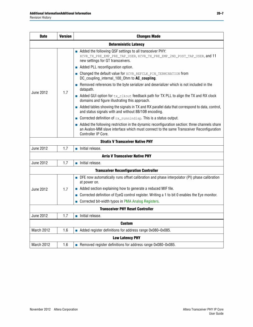
Additional InformationAdditional Information 20–7Revision History
Deterministic Latency
June 2012 1.7
■ Added the following QSF settings to all transceiver PHY: XCVR_TX_PRE_EMP_PRE_TAP_USER, XCVR_TX_PRE_EMP_2ND_POST_TAP_USER, and 11 new settings for GT transceivers.
■ Added PLL reconfiguration option.
■ Changed the default value for XCVR_REFCLK_PIN_TERMINATION from DC_coupling_internal_100_Ohm to AC_coupling.
■ Removed references to the byte serializer and deserializer which is not included in the datapath.
■ Added GUI option for tx_clkout feedback path for TX PLL to align the TX and RX clock domains and figure illustrating this approach.
■ Added tables showing the signals in TX and RX parallel data that correspond to data, control, and status signals with and without 8B/10B encoding.
■ Corrected definition of rx_runnindisp. This is a status output.
■ Added the following restriction in the dynamic reconfiguration section: three channels share an Avalon-MM slave interface which must connect to the same Transceiver Reconfiguration Controller IP Core.
Stratix V Transceiver Native PHY
June 2012 1.7 ■ Initial release.
Arria V Transceiver Native PHY
June 2012 1.7 ■ Initial release.
Transceiver Reconfiguration Controller
June 2012 1.7
■ DFE now automatically runs offset calibration and phase interpolator (PI) phase calibration at power on.
■ Added section explaining how to generate a reduced MIF file.
■ Corrected definition of EyeQ control register. Writing a 1 to bit 0 enables the Eye monitor.
■ Corrected bit-width typos in PMA Analog Registers.
Transceiver PHY Reset Controller
June 2012 1.7 ■ Initial release.
Custom
March 2012 1.6 ■ Added register definitions for address range 0x080–0x085.
Low Latency PHY
March 2012 1.6 ■ Removed register definitions for address range 0x080–0x085.
Date Version Changes Made
November 2012 Altera Corporation Altera Transceiver PHY IP CoreUser Guide
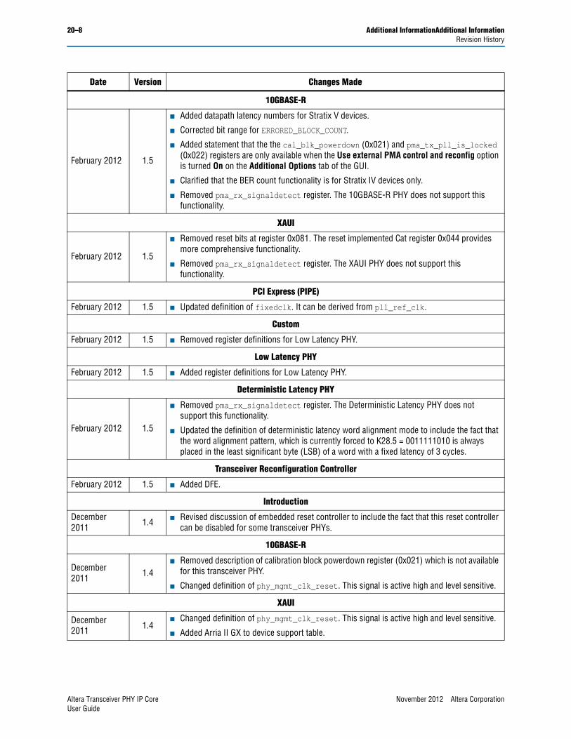
20–8 Additional InformationAdditional InformationRevision History
10GBASE-R
February 2012 1.5
■ Added datapath latency numbers for Stratix V devices.
■ Corrected bit range for ERRORED_BLOCK_COUNT.
■ Added statement that the the cal_blk_powerdown (0x021) and pma_tx_pll_is_locked (0x022) registers are only available when the Use external PMA control and reconfig option is turned On on the Additional Options tab of the GUI.
■ Clarified that the BER count functionality is for Stratix IV devices only.
■ Removed pma_rx_signaldetect register. The 10GBASE-R PHY does not support this functionality.
XAUI
February 2012 1.5
■ Removed reset bits at register 0x081. The reset implemented Cat register 0x044 provides more comprehensive functionality.
■ Removed pma_rx_signaldetect register. The XAUI PHY does not support this functionality.
PCI Express (PIPE)
February 2012 1.5 ■ Updated definition of fixedclk. It can be derived from pll_ref_clk.
Custom
February 2012 1.5 ■ Removed register definitions for Low Latency PHY.
Low Latency PHY
February 2012 1.5 ■ Added register definitions for Low Latency PHY.
Deterministic Latency PHY
February 2012 1.5
■ Removed pma_rx_signaldetect register. The Deterministic Latency PHY does not support this functionality.
■ Updated the definition of deterministic latency word alignment mode to include the fact that the word alignment pattern, which is currently forced to K28.5 = 0011111010 is always placed in the least significant byte (LSB) of a word with a fixed latency of 3 cycles.
Transceiver Reconfiguration Controller
February 2012 1.5 ■ Added DFE.
Introduction
December 2011 1.4 ■ Revised discussion of embedded reset controller to include the fact that this reset controller
can be disabled for some transceiver PHYs.
10GBASE-R
December 2011 1.4
■ Removed description of calibration block powerdown register (0x021) which is not available for this transceiver PHY.
■ Changed definition of phy_mgmt_clk_reset. This signal is active high and level sensitive.
XAUI
December 2011 1.4
■ Changed definition of phy_mgmt_clk_reset. This signal is active high and level sensitive.
■ Added Arria II GX to device support table.
Date Version Changes Made
Altera Transceiver PHY IP Core November 2012 Altera CorporationUser Guide

Additional InformationAdditional Information 20–9Revision History
Interlaken
December 2011 1.4
■ Changed access mode for RX equalization, pre-CDR reverse serial loopback, and post-CDR reverse serial loopback to write only (WO).
■ Removed optional rx_sync_word_err, rx_scrm_err, and rx_framing_err status bits.
■ Changed definition of phy_mgmt_clk_reset. This signal is active high and level sensitive.
PHY IP Core for PCI Express (PIPE)
December 2011 1.4 ■ Changed definition of phy_mgmt_clk_reset. This signal is active high and level sensitive.
Custom
December 2011 1.4
■ Added ×N and feedback compensation options for bonded clocks.
■ Added Enable Channel Interface parameter which is required for dynamic reconfiguration of transceivers.
■ Corrected formulas for signal width in top-level signals figure.
■ Changed definition of phy_mgmt_clk_reset. This signal is active high and level sensitive.
Low Latency PHY
December 2011 1.4
■ Added option to disable the embedded reset controller to allow you to create your own reset sequence.
■ Added ×N and feedback compensation options for bonded clocks.
■ Fixed name of phy_mgmt_reset signal. Should be phy_mgmt_clk_reset. Also, a positive edge on this signal initiates a reset.
■ Added Enable Channel Interface parameter which is required for dynamic reconfiguration of transceivers.
■ Corrected formulas for signal width in top-level signals figure.
■ Changed definition of phy_mgmt_clk_reset. This signal is active high and level sensitive.
Deterministic Latency PHY
December 2011 1.4
■ Removed Enable tx_clkout feedback path for TX PLL from the General Options tab of the Deterministic Latency PHY IP Core GUI. This option is unavailable in 11.1 and 11.1 SP1.
■ Changed definition of phy_mgmt_clk_reset. This signal is active high and level sensitive.
Transceiver Reconfiguration Controller
December 2011 1.4
■ Added duty cycle distortion (DCD) signal integrity feature.
■ Added PLL and channel reconfiguration using a memory initialization file (.mif).
■ Added ability to reconfigure PLLs, including the input reference clock or to change the PLL that supplies the high speed serial clock to the serializer without including logic to reconfigure channels.
■ Corrected values for RX equalization gain. 0–4 are available.
■ Corrected logical number in Interface Ordering with Multiple Transceiver PHY Instances.
■ Increased the number of channels that can share a PLL from 5 to 11 when feedback compensation is used.
■ Increased the number of channels that can connect to the Transceiver Reconfiguration Controller from 32 to 64.
■ Added section on requirements for merging PLLs.
Date Version Changes Made
November 2012 Altera Corporation Altera Transceiver PHY IP CoreUser Guide
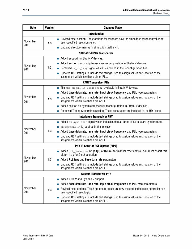
20–10 Additional InformationAdditional InformationRevision History
Introduction
November 2011 1.3
■ Revised reset section. The 2 options for reset are now the embedded reset controller or user-specified reset controller.
■ Updated directory names in simulation testbench.
10GBASE-R PHY Transceiver
November 2011 1.3
■ Added support for Stratix V devices.
■ Added section discussing transceiver reconfiguration in Stratix V devices.
■ Removed rx_oc_busy signal which is included in the reconfiguration bus.
■ Updated QSF settings to include text strings used to assign values and location of the assignment which is either a pin or PLL.
XAUI Transceiver PHY
November
20111.3
■ The pma_tx_pll_is_locked is not available in Stratix V devices.
■ Added base data rate, lane rate, input clock frequency, and PLL type parameters.
■ Updated QSF settings to include text strings used to assign values and location of the assignment which is either a pin or PLL.
■ Added section on dynamic transceiver reconfiguration in Stratix V devices.
■ Removed Timing Constraints section. These constraints are included in the HDL code.
Interlaken Transceiver PHY
November 2011 1.3
■ Added tx_sync_done signal which indicates that all lanes of TX data are synchronized.
■ tx_coreclk_in is required in this release.
■ Added base data rate, lane rate, input clock frequency, and PLL type parameters.
■ Updated QSF settings to include text strings used to assign values and location of the assignment which is either a pin or PLL.
PHY IP Core for PCI Express (PIPE)
November 2011 1.3
■ Added pll_powerdown bit (bit[0] of 0x044) for manual reset control. You must assert this bit for 1 s for Gen2 operation.
■ Added PLL type and base data rate parameters.
■ Updated QSF settings to include text strings used to assign values and location of the assignment which is either a pin or PLL.
Custom Transceiver PHY
November 2011 1.3
■ Added Arria V and Cyclone V support.
■ Added base data rate, lane rate, input clock frequency, and PLL type parameters.
■ Revised reset options. The 2 options for reset are now the embedded reset controller or a user-specified reset logic.
■ Updated QSF settings to include text strings used to assign values and location of the assignment which is either a pin or PLL.
Date Version Changes Made
Altera Transceiver PHY IP Core November 2012 Altera CorporationUser Guide
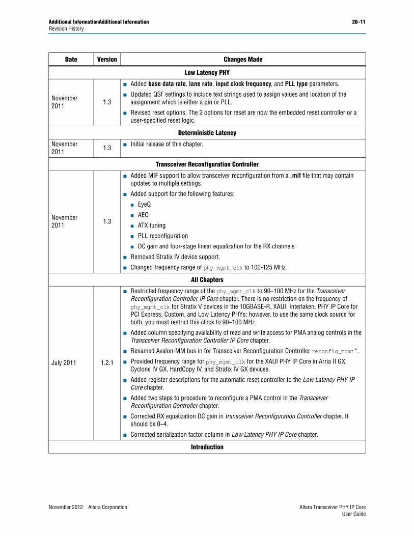
Additional InformationAdditional Information 20–11Revision History
Low Latency PHY
November 2011 1.3
■ Added base data rate, lane rate, input clock frequency, and PLL type parameters.
■ Updated QSF settings to include text strings used to assign values and location of the assignment which is either a pin or PLL.
■ Revised reset options. The 2 options for reset are now the embedded reset controller or a user-specified reset logic.
Deterministic Latency
November 2011 1.3 ■ Initial release of this chapter.
Transceiver Reconfiguration Controller
November 2011 1.3
■ Added MIF support to allow transceiver reconfiguration from a .mif file that may contain updates to multiple settings.
■ Added support for the following features:
■ EyeQ
■ AEQ
■ ATX tuning
■ PLL reconfiguration
■ DC gain and four-stage linear equalization for the RX channels
■ Removed Stratix IV device support.
■ Changed frequency range of phy_mgmt_clk to 100-125 MHz.
All Chapters
July 2011 1.2.1
■ Restricted frequency range of the phy_mgmt_clk to 90–100 MHz for the Transceiver Reconfiguration Controller IP Core chapter. There is no restriction on the frequency of phy_mgmt_clk for Stratix V devices in the 10GBASE-R, XAUI, Interlaken, PHY IP Core for PCI Express, Custom, and Low Latency PHYs; however, to use the same clock source for both, you must restrict this clock to 90–100 MHz.
■ Added column specifying availability of read and write access for PMA analog controls in the Transceiver Reconfiguration Controller IP Core chapter.
■ Renamed Avalon-MM bus in for Transceiver Reconfiguration Controller reconfig_mgmt*.
■ Provided frequency range for phy_mgmt_clk for the XAUI PHY IP Core in Arria II GX, Cyclone IV GX, HardCopy IV, and Stratix IV GX devices.
■ Added register descriptions for the automatic reset controller to the Low Latency PHY IP Core chapter.
■ Added two steps to procedure to reconfigure a PMA control in the Transceiver Reconfiguration Controller chapter.
■ Corrected RX equalization DC gain in transceiver Reconfiguration Controller chapter. It should be 0–4.
■ Corrected serialization factor column in Low Latency PHY IP Core chapter.
Introduction
Date Version Changes Made
November 2012 Altera Corporation Altera Transceiver PHY IP CoreUser Guide
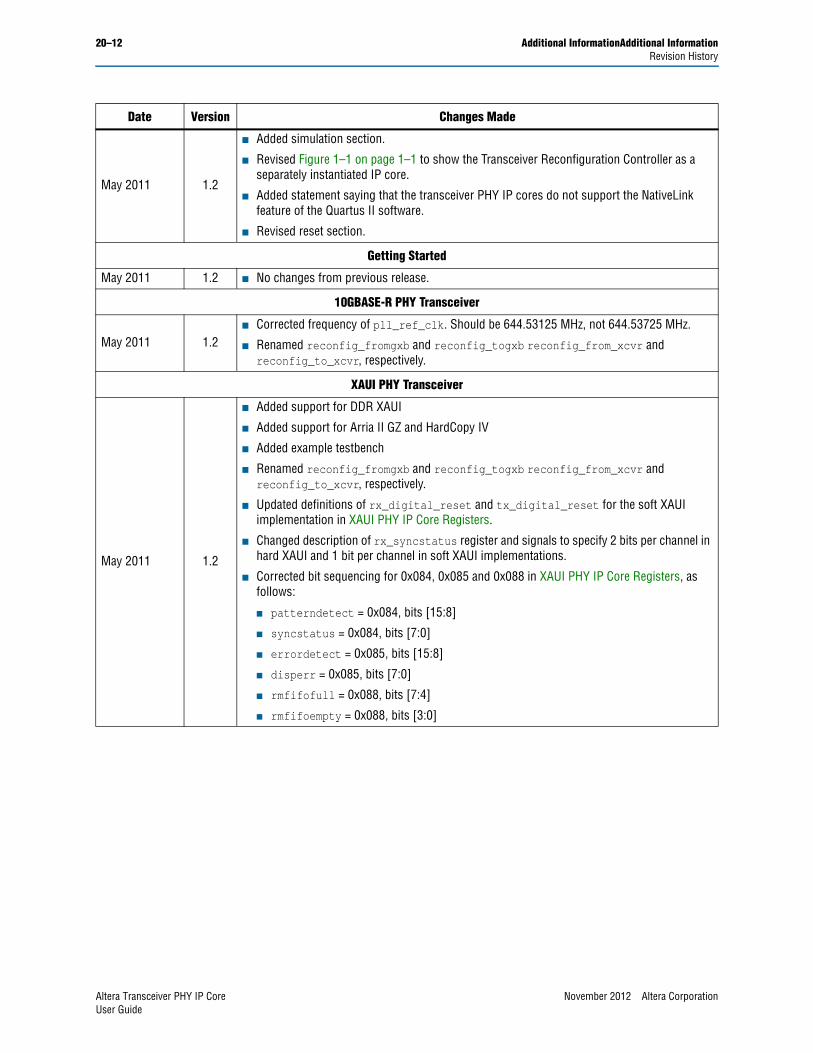
20–12 Additional InformationAdditional InformationRevision History
May 2011 1.2
■ Added simulation section.
■ Revised Figure 1–1 on page 1–1 to show the Transceiver Reconfiguration Controller as a separately instantiated IP core.
■ Added statement saying that the transceiver PHY IP cores do not support the NativeLink feature of the Quartus II software.
■ Revised reset section.
Getting Started
May 2011 1.2 ■ No changes from previous release.
10GBASE-R PHY Transceiver
May 2011 1.2■ Corrected frequency of pll_ref_clk. Should be 644.53125 MHz, not 644.53725 MHz.
■ Renamed reconfig_fromgxb and reconfig_togxb reconfig_from_xcvr and reconfig_to_xcvr, respectively.
XAUI PHY Transceiver
May 2011 1.2
■ Added support for DDR XAUI
■ Added support for Arria II GZ and HardCopy IV
■ Added example testbench
■ Renamed reconfig_fromgxb and reconfig_togxb reconfig_from_xcvr and reconfig_to_xcvr, respectively.
■ Updated definitions of rx_digital_reset and tx_digital_reset for the soft XAUI implementation in XAUI PHY IP Core Registers.
■ Changed description of rx_syncstatus register and signals to specify 2 bits per channel in hard XAUI and 1 bit per channel in soft XAUI implementations.
■ Corrected bit sequencing for 0x084, 0x085 and 0x088 in XAUI PHY IP Core Registers, as follows:
■ patterndetect = 0x084, bits [15:8]
■ syncstatus = 0x084, bits [7:0]
■ errordetect = 0x085, bits [15:8]
■ disperr = 0x085, bits [7:0]
■ rmfifofull = 0x088, bits [7:4]
■ rmfifoempty = 0x088, bits [3:0]
Date Version Changes Made
Altera Transceiver PHY IP Core November 2012 Altera CorporationUser Guide
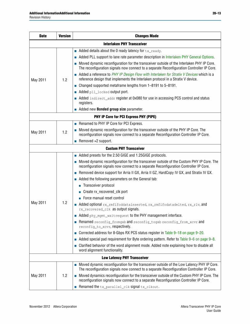
Additional InformationAdditional Information 20–13Revision History
Interlaken PHY Transceiver
May 2011 1.2
■ Added details about the 0 ready latency for tx_ready.
■ Added PLL support to lane rate parameter description in Interlaken PHY General Options.
■ Moved dynamic reconfiguration for the transceiver outside of the Interlaken PHY IP Core. The reconfiguration signals now connect to a separate Reconfiguration Controller IP Core.
■ Added a reference to PHY IP Design Flow with Interlaken for Stratix V Devices which is a reference design that implements the Interlaken protocol in a Stratix V device.
■ Changed supported metaframe lengths from 1–8191 to 5–8191.
■ Added pll_locked output port.
■ Added indirect_addr register at 0x080 for use in accessing PCS control and status registers.
■ Added new Bonded group size parameter.
PHY IP Core for PCI Express PHY (PIPE)
May 2011 1.2
■ Renamed to PHY IP Core for PCI Express.
■ Moved dynamic reconfiguration for the transceiver outside of the PHY IP Core. The reconfiguration signals now connect to a separate Reconfiguration Controller IP Core.
■ Removed ×2 support.
Custom PHY Transceiver
May 2011 1.2
■ Added presets for the 2.50 GIGE and 1.25GIGE protocols.
■ Moved dynamic reconfiguration for the transceiver outside of the Custom PHY IP Core. The reconfiguration signals now connect to a separate Reconfiguration Controller IP Core.
■ Removed device support for Arria II GX, Arria II GZ, HardCopy IV GX, and Stratix IV GX.
■ Added the following parameters on the General tab:
■ Transceiver protocol
■ Create rx_recovered_clk port
■ Force manual reset control
■ Added optional rx_rmfifoddatainserted, rx_rmfifodatadelted, rx_rlv, and rx_recovered_clk as output signals.
■ Added phy_mgmt_waitrequest to the PHY management interface.
■ Renamed reconfig_fromgxb and reconfig_togxb reconfig_from_xcvr and reconfig_to_xcvr, respectively.
■ Corrected address for 8-Gbps RX PCS status register in Table 9–18 on page 9–20.
■ Added special pad requirement for Byte ordering pattern. Refer to Table 9–6 on page 9–8.
■ Clarified behavior of the word alignment mode. Added note explaining how to disable all word alignment functionality.
Low Latency PHY Transceiver
May 2011 1.2
■ Moved dynamic reconfiguration for the transceiver outside of the Low Latency PHY IP Core. The reconfiguration signals now connect to a separate Reconfiguration Controller IP Core.
■ Moved dynamics reconfiguration for the transceiver outside of the Custom PHY IP Core. The reconfiguration signals now connect to a separate Reconfiguration Controller IP Core.
■ Renamed the tx_parallel_clk signal tx_clkout.
Date Version Changes Made
November 2012 Altera Corporation Altera Transceiver PHY IP CoreUser Guide
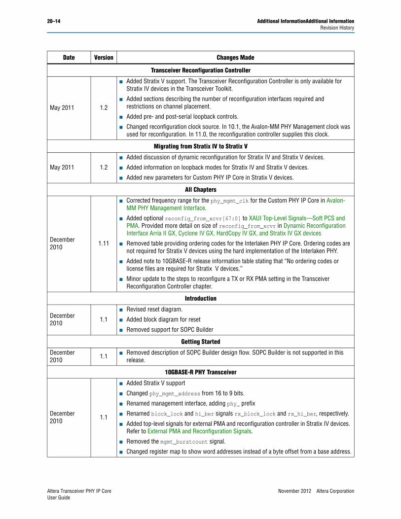
20–14 Additional InformationAdditional InformationRevision History
Transceiver Reconfiguration Controller
May 2011 1.2
■ Added Stratix V support. The Transceiver Reconfiguration Controller is only available for Stratix IV devices in the Transceiver Toolkit.
■ Added sections describing the number of reconfiguration interfaces required and restrictions on channel placement.
■ Added pre- and post-serial loopback controls.
■ Changed reconfiguration clock source. In 10.1, the Avalon-MM PHY Management clock was used for reconfiguration. In 11.0, the reconfiguration controller supplies this clock.
Migrating from Stratix IV to Stratix V
May 2011 1.2
■ Added discussion of dynamic reconfiguration for Stratix IV and Stratix V devices.
■ Added information on loopback modes for Stratix IV and Stratix V devices.
■ Added new parameters for Custom PHY IP Core in Stratix V devices.
All Chapters
December2010 1.11
■ Corrected frequency range for the phy_mgmt_clk for the Custom PHY IP Core in Avalon-MM PHY Management Interface.
■ Added optional reconfig_from_xcvr[67:0] to XAUI Top-Level Signals—Soft PCS and PMA. Provided more detail on size of reconfig_from_xcvr in Dynamic Reconfiguration Interface Arria II GX, Cyclone IV GX, HardCopy IV GX, and Stratix IV GX devices
■ Removed table providing ordering codes for the Interlaken PHY IP Core. Ordering codes are not required for Stratix V devices using the hard implementation of the Interlaken PHY.
■ Added note to 10GBASE-R release information table stating that “No ordering codes or license files are required for Stratix V devices.”
■ Minor update to the steps to reconfigure a TX or RX PMA setting in the Transceiver Reconfiguration Controller chapter.
Introduction
December 2010 1.1
■ Revised reset diagram.
■ Added block diagram for reset
■ Removed support for SOPC Builder
Getting Started
December 2010 1.1 ■ Removed description of SOPC Builder design flow. SOPC Builder is not supported in this
release.
10GBASE-R PHY Transceiver
December 2010 1.1
■ Added Stratix V support
■ Changed phy_mgmt_address from 16 to 9 bits.
■ Renamed management interface, adding phy_ prefix
■ Renamed block_lock and hi_ber signals rx_block_lock and rx_hi_ber, respectively.
■ Added top-level signals for external PMA and reconfiguration controller in Stratix IV devices. Refer to External PMA and Reconfiguration Signals.
■ Removed the mgmt_burstcount signal.
■ Changed register map to show word addresses instead of a byte offset from a base address.
Date Version Changes Made
Altera Transceiver PHY IP Core November 2012 Altera CorporationUser Guide

Additional InformationAdditional Information 20–15Revision History
XAUI PHY Transceiver
December 2010 1.1
■ Added support for Arria II GX and Cyclone IV GX with hard PCS
■ Renamed management interface, adding phy_ prefix
■ Changed phy_mgmt_address from 16 to 9 bits.
■ Renamed many signals. Refer to XAUI Top-Level Signals—Soft PCS and PMA and “XAUI Top-Level Signals–Hard IP PCS and PMA” as appropriate.
■ Changed register map to show word addresses instead of a byte offset from a base address.
■ Removed the rx_ctrldetect and rx_freqlocked signals.
Interlaken PHY Transceiver
December 2010 1.1
■ Added simulation support in ModelSim SE, Synopsys VCS MX, Cadence NCSim
■ Changed number of lanes supported from 4–24 to 1–24.
■ Changed reference clock to be 1/20th rather than 1/10th the lane rate.
■ Renamed management interface, adding phy_ prefix
■ Changed phy_mgmt_address from 16 to 9 bits.
■ Changed many signal names, refer to Top-Level Interlaken PHY Signals.Changed register map to show word addresses instead of a byte offset from a base address.
PCI Express PHY (PIPE)
December 2010 1.1
■ Added simulation support in ModelSim SE
■ Added PIPE low latency configuration option
■ Changed phy_mgmt_address from 16 to 9 bits.
■ Changed register map to show word addresses instead of a byte offset from a base address.
■ Added tx_ready, rx_ready, pipe_txswing, and pipe_rxeleciidle signals
■ Added rx_errdetect, rx_disperr, and rx_a1a2sizeout register fields
Custom PHY Transceiver
December 2010 1.1
■ Added support for 8B/10B encoding and decoding in Stratix V devices
■ Added support for rate matching in Stratix V devices.
■ Added support for Arria II GX, Arria II GZ, HardCopy IV GX, and Stratix IV GX devices
■ Renamed management interface, adding phy_ prefix
■ Changed phy_mgmt_address from 8 to 9 bits.
■ Added many optional status ports and renamed some signals. Refer to Figure 9–2 on page 9–15 and subsequent signal descriptions.
■ Changed register map to show word addresses instead of a byte offset from a base address.
Low Latency PHY IP Core
December 2010 1.1
■ Renamed management interface, adding phy_ prefix
■ Changed phy_mgmt_address from 16 to 9 bits.
■ Changed register map to show word addresses instead of a byte offset from a base address.
■ Removed rx_offset_cancellation_done signal. Internal reset logic determines when offset cancellation has completed.
■ Removed support for Stratix IV GX devices.
Date Version Changes Made
November 2012 Altera Corporation Altera Transceiver PHY IP CoreUser Guide
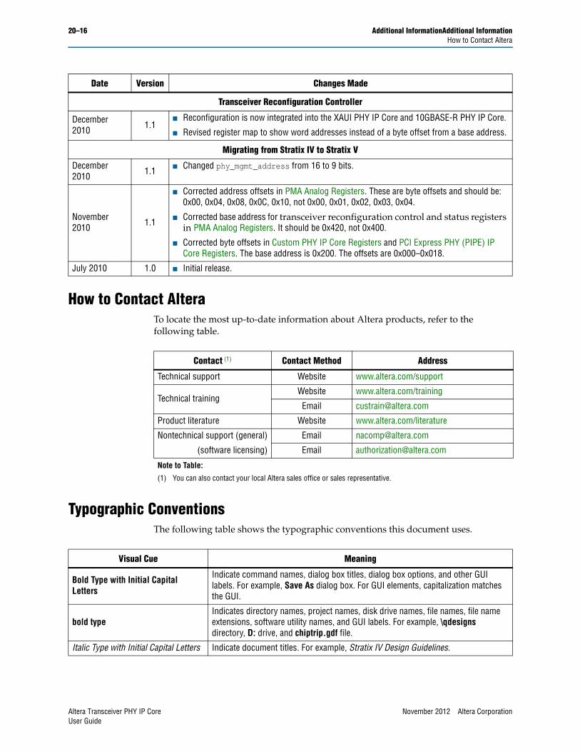
20–16 Additional InformationAdditional InformationHow to Contact Altera
How to Contact AlteraTo locate the most up-to-date information about Altera products, refer to the following table.
Typographic ConventionsThe following table shows the typographic conventions this document uses.
Transceiver Reconfiguration Controller
December 2010 1.1
■ Reconfiguration is now integrated into the XAUI PHY IP Core and 10GBASE-R PHY IP Core.
■ Revised register map to show word addresses instead of a byte offset from a base address.
Migrating from Stratix IV to Stratix V
December 2010 1.1 ■ Changed phy_mgmt_address from 16 to 9 bits.
November 2010 1.1
■ Corrected address offsets in PMA Analog Registers. These are byte offsets and should be: 0x00, 0x04, 0x08, 0x0C, 0x10, not 0x00, 0x01, 0x02, 0x03, 0x04.
■ Corrected base address for transceiver reconfiguration control and status registers in PMA Analog Registers. It should be 0x420, not 0x400.
■ Corrected byte offsets in Custom PHY IP Core Registers and PCI Express PHY (PIPE) IP Core Registers. The base address is 0x200. The offsets are 0x000–0x018.
July 2010 1.0 ■ Initial release.
Date Version Changes Made
Contact (1) Contact Method Address
Technical support Website www.altera.com/support
Technical trainingWebsite www.altera.com/training
Email [email protected]
Product literature Website www.altera.com/literature
Nontechnical support (general) Email [email protected]
(software licensing) Email [email protected]
Note to Table:
(1) You can also contact your local Altera sales office or sales representative.
Visual Cue Meaning
Bold Type with Initial Capital Letters
Indicate command names, dialog box titles, dialog box options, and other GUI labels. For example, Save As dialog box. For GUI elements, capitalization matches the GUI.
bold typeIndicates directory names, project names, disk drive names, file names, file name extensions, software utility names, and GUI labels. For example, \qdesigns directory, D: drive, and chiptrip.gdf file.
Italic Type with Initial Capital Letters Indicate document titles. For example, Stratix IV Design Guidelines.
Altera Transceiver PHY IP Core November 2012 Altera CorporationUser Guide
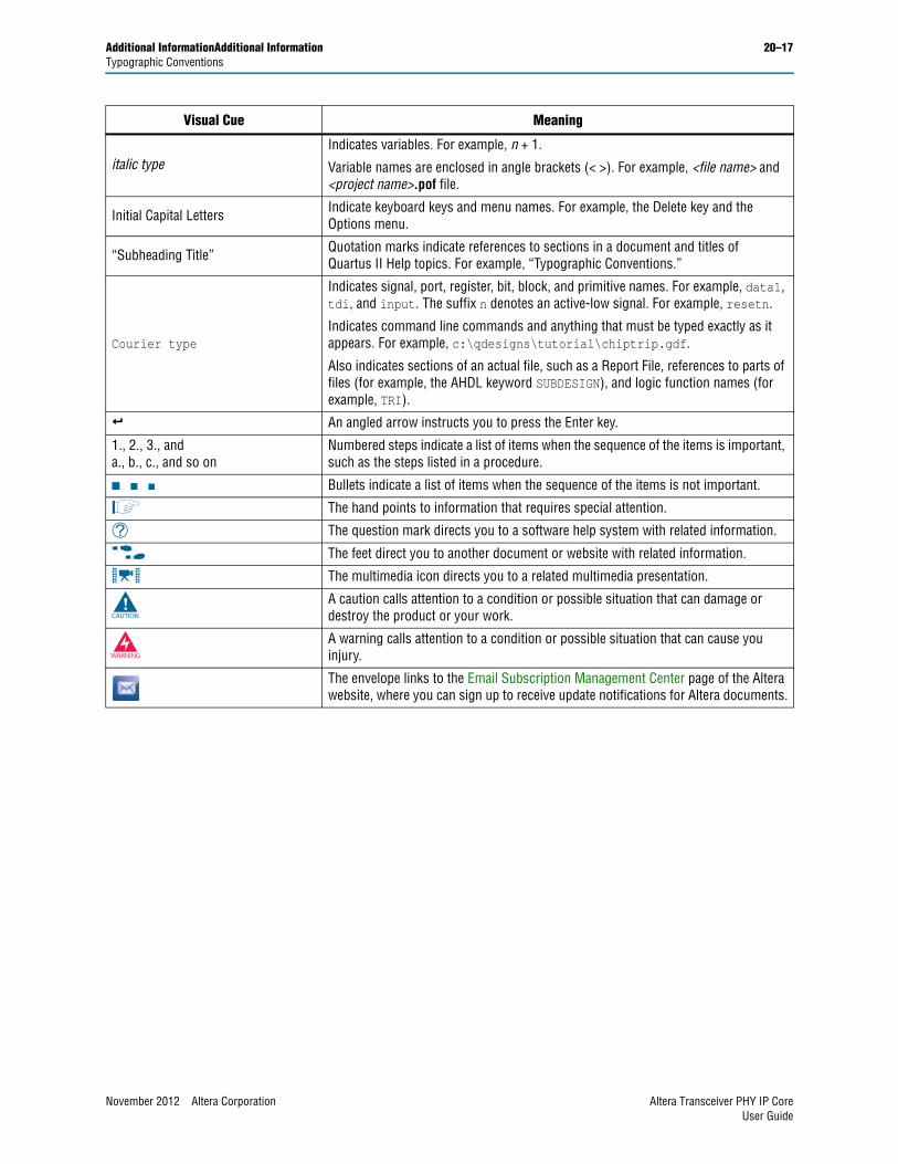
Additional InformationAdditional Information 20–17Typographic Conventions
italic typeIndicates variables. For example, n + 1.
Variable names are enclosed in angle brackets (< >). For example, <file name> and <project name>.pof file.
Initial Capital Letters Indicate keyboard keys and menu names. For example, the Delete key and the Options menu.
“Subheading Title” Quotation marks indicate references to sections in a document and titles of Quartus II Help topics. For example, “Typographic Conventions.”
Courier type
Indicates signal, port, register, bit, block, and primitive names. For example, data1, tdi, and input. The suffix n denotes an active-low signal. For example, resetn.
Indicates command line commands and anything that must be typed exactly as it appears. For example, c:\qdesigns\tutorial\chiptrip.gdf.
Also indicates sections of an actual file, such as a Report File, references to parts of files (for example, the AHDL keyword SUBDESIGN), and logic function names (for example, TRI).
r An angled arrow instructs you to press the Enter key.
1., 2., 3., anda., b., c., and so on
Numbered steps indicate a list of items when the sequence of the items is important, such as the steps listed in a procedure.
■ ■ ■ Bullets indicate a list of items when the sequence of the items is not important.
1 The hand points to information that requires special attention.
h The question mark directs you to a software help system with related information.
f The feet direct you to another document or website with related information.
m The multimedia icon directs you to a related multimedia presentation.
c A caution calls attention to a condition or possible situation that can damage or destroy the product or your work.
w A warning calls attention to a condition or possible situation that can cause you injury.
The envelope links to the Email Subscription Management Center page of the Altera website, where you can sign up to receive update notifications for Altera documents.
Visual Cue Meaning
November 2012 Altera Corporation Altera Transceiver PHY IP CoreUser Guide

20–18 Additional InformationAdditional InformationTypographic Conventions
Altera Transceiver PHY IP Core November 2012 Altera CorporationUser Guide