altera transceiver phy ip core user guide...altera transceiver phy ip core user guide 101 innovation...
TRANSCRIPT

Altera Transceiver PHY IP Core User Guide
101 Innovation DriveSan Jose, CA 95134www.altera.com
UG-010802013.4.25
Subscribe
Feedback

Contents
Introduction to the Protocol-Specific and Native Transceiver PHYs...............1-1Protocol-Specific Transceiver PHYs.........................................................................................................1-1Native Transceiver PHYs ...........................................................................................................................1-2Non-Protocol-Specific Transceiver PHYs................................................................................................1-4Transceiver PHY Modules..........................................................................................................................1-4Transceiver Reconfiguration Controller...................................................................................................1-5Resetting the Transceiver PHY..................................................................................................................1-5Running a Simulation Testbench..............................................................................................................1-6Unsupported Features.................................................................................................................................1-8
Getting Started Overview....................................................................................2-1Installation and Licensing of IP Cores......................................................................................................2-1Design Flows.................................................................................................................................................2-2MegaWizard Plug-In Manager Flow.........................................................................................................2-2
Specifying Parameters.....................................................................................................................2-3Simulate the IP Core........................................................................................................................2-4
10GBASE-R PHY P Core.....................................................................................3-110GBASE-R PHY Release Information....................................................................................................3-510GBASE-R PHY Device Family Support................................................................................................3-510GBASE-R PHY Performance and Resource Utilization for Stratix IV Devices..............................3-610GBASE-R PHY Performance and Resource Utilization for Arria V GT Devices..........................3-610GBASE-R PHY Performance and Resource Utilization for Arria V GZ and Stratix V
Devices.....................................................................................................................................................3-6Parameterizing the 10GBASE-R PHY.......................................................................................................3-7General Option Parameters........................................................................................................................3-7Analog Parameters for Stratix IV Devices................................................................................................3-910GBASE-R PHY Interfaces.....................................................................................................................3-1110GBASE-R PHY Data Interfaces...........................................................................................................3-1110GBASE-R PHY Status, 1588, and PLL Reference Clock Interfaces................................................3-1510GBASE-R PHY Clocks for Arria V GT Devices................................................................................3-1610GBASE-R PHY Clocks for Arria V GZ Devices................................................................................3-1610GBASE-R PHY Clocks for Stratix IV Devices...................................................................................3-17
Altera Corporation
TOC-2

10GBASE-R PHY Clocks for Stratix V Devices.....................................................................................3-1810GBASE-R PHY Register Interface and Register Descriptions.........................................................3-1910GBASE-R PHY Dynamic Reconfiguration for Stratix IV Devices.................................................3-2310GBASE-R PHY Dynamic Reconfiguration for Arria V and Stratix V Devices.............................3-2310GBASE-R PHY TimeQuest Timing Constraints..............................................................................3-2410GBASE-R PHY Simulation Files and Example Testbench..............................................................3-27
Backplane Ethernet 10GBASE-KR PHY IP Core...............................................4-110GBASE-KR PHY Release Information.................................................................................................4-2Device Family Support................................................................................................................................4-210GBASE-KR PHY Performance and Resource Utilization..................................................................4-3Parameterizing the 10GBASE-KR PHY....................................................................................................4-3
10GBASE-KR Link Training Parameters ....................................................................................4-410GBASE-KR Auto-Negotiation Parameters..............................................................................4-510GBASE-R Parameters..................................................................................................................4-61GbE Parameters..............................................................................................................................4-61G/10GbE Speed Detection Parameters.......................................................................................4-71G/10GbE PHY Analog Parameters.............................................................................................4-8
10GBASE-KR PHY IP Core Functional Description..............................................................................4-810BASE-KR PHY Interfaces.....................................................................................................................4-1310GBASE-KR PHY Clock and Reset Interfaces....................................................................................4-14
10GBASE-KR PHY Data Interfaces............................................................................................4-1510GBASE-KR PHY Control and Status Interfaces....................................................................4-1810GBASE-KR PHY Link Training..............................................................................................4-1910GBASE-KR PHY Daisy-Chain Mode.....................................................................................4-2010GBASE-KR PHY Daisy-Chain Interface Signals...................................................................4-211G/10GbE PHY Embedded Processor Interface Signals..........................................................4-22
Register Interface Signals..........................................................................................................................4-2310GBASE-KR PHY Register Definitions................................................................................................4-24PMA Registers............................................................................................................................................4-35PCS Registers..............................................................................................................................................4-36PMA Registers............................................................................................................................................4-3710GBASE-KR Dynamic Reconfiguration from 1G to 10GbE.............................................................4-3810GBASE-KR PHY Arbitration Logic Requirements...........................................................................4-3910GBASE-KR PHY State Machine Logic Requirements......................................................................4-39Creating a 10GBASE-KR Design.............................................................................................................4-39Editing a 10GBASE-KR MIF File ...........................................................................................................4-40Design Example..........................................................................................................................................4-41
Altera Corporation
TOC-3

Acronyms....................................................................................................................................................4-41
1G/10 Gbps Ethernet PHY IP Core.....................................................................5-11G/10GbE PHY Release Information.......................................................................................................5-2Device Family Support................................................................................................................................5-21G/10GbE PHY Performance and Resource Utilization........................................................................5-3Parameterizing the 1G/10GbE PHY..........................................................................................................5-3
1GbE Parameters..............................................................................................................................5-41G/10GbE Speed Detection Parameters.......................................................................................5-41G/10GbE PHY Analog Parameters.............................................................................................5-5
1G/10GbE PHY Interfaces..........................................................................................................................5-61G/10GbE PHY Clock and Reset Interfaces................................................................................5-71G/10GbE PHY Data Interfaces....................................................................................................5-81G/10GbE PHY XGMII Mapping to Standard SDR XGMII Data...........................................5-91G/10GbE PHY Serial Data Interface.........................................................................................5-111G/10GbE Control and Status Interfaces...................................................................................5-11Register Interface Signals..............................................................................................................5-12
1G/10GbE PHY Register Definitions .....................................................................................................5-13PMA Registers............................................................................................................................................5-14PCS Registers..............................................................................................................................................5-141G/10GbE GMII PCS Registers...............................................................................................................5-15PMA Registers............................................................................................................................................5-171G/10GbE Dynamic Reconfiguration from 1G to 10GbE...................................................................5-18
1G/10GbE PHY Arbitration Logic Requirements.....................................................................5-191G/10GbE PHY State Machine Logic Requirements................................................................5-20Editing a 1G/10GbE MIF File .....................................................................................................5-20Creating a 1G/10GbE Design.......................................................................................................5-21Dynamic Reconfiguration Interface Signals..............................................................................5-22
Design Example..........................................................................................................................................5-231G/10GbE PHY IP Core Simulation Support........................................................................................5-231G/10GbE TimeQuest Timing Constraints...........................................................................................5-23Acronyms....................................................................................................................................................5-23
XAUI PHY IP Core.............................................................................................6-1XAUI PHY Release Information...............................................................................................................6-1XAUI PHY Device Family Support...........................................................................................................6-2XAUI PHY Performance and Resource Utilization for Stratix IV Devices.........................................6-3XAUI PHY Performance and Resource Utilization for Arria V GZ and Stratix V Devices.............6-3
Altera Corporation
TOC-4

Parameterizing the XAUI PHY..................................................................................................................6-3XAUI PHY General Parameters................................................................................................................6-4XAUI PHY Analog Parameters..................................................................................................................6-6XAUI PHY Analog Parameters for Arria II GX, Cyclone IV GX, HardCopy IV and Stratix IV
Devices.....................................................................................................................................................6-6Advanced Options Parameters..................................................................................................................6-8XAUI PHY Configurations........................................................................................................................6-8XAUI PHY Ports..........................................................................................................................................6-9XAUI PHY Data Interfaces......................................................................................................................6-11
SDR XGMII TX Interface.............................................................................................................6-12SDR XGMII RX Interface.............................................................................................................6-13Transceiver Serial Data Interface.................................................................................................6-13
XAUI PHY Clocks, Reset, and Powerdown Interfaces.........................................................................6-13XAUI PHY PMA Channel Controller Interface....................................................................................6-15XAUI PHY Optional PMA Control and Status Interface....................................................................6-15XAUI PHY Register Interface and Register Descriptions....................................................................6-18XAUI PHY Dynamic Reconfiguration for Arria II GX, Cyclone IV GX, HardCopy IV GX, and
Stratix IV GX.........................................................................................................................................6-24XAUI PHY Dynamic Reconfiguration for Arria V, Cyclone V and Stratix V Devices...................6-25
Logical Lane Assignment Restriction..........................................................................................6-26XAUI PHY Dynamic Reconfiguration Interface Signals.........................................................6-26
Simulation Files and Example Testbench...............................................................................................6-27
Interlaken PHY IP Core......................................................................................7-1Interlaken PHY Device Family Support...................................................................................................7-2Parameterizing the Interlaken PHY..........................................................................................................7-3Interlaken PHY General Parameters.........................................................................................................7-3Interlaken PHY Optional Port Parameters..............................................................................................7-5Interlaken PHY Analog Parameters..........................................................................................................7-5Interlaken PHY Interfaces..........................................................................................................................7-6Interlaken PHY Avalon-ST TX Interface.................................................................................................7-6Interlaken PHY Avalon-ST RX Interface...............................................................................................7-10Interlaken PHY TX and RX Serial Interface..........................................................................................7-14Interlaken PHY PLL Interface..................................................................................................................7-14Interlaken Optional Clocks for Deskew..................................................................................................7-15Interlaken PHY Register Interface and Register Descriptions............................................................7-15Why Transceiver Dynamic Reconfiguration.........................................................................................7-19Dynamic Transceiver Reconfiguration Interface..................................................................................7-20
Altera Corporation
TOC-5

Interlaken PHY TimeQuest Timing Constraints..................................................................................7-21Interlaken PHY Simulation Files and Example Testbench..................................................................7-21
PHY IP Core for PCI Express (PIPE) .................................................................8-1PHY for PCIe (PIPE) Device Family Support..........................................................................................8-3PHY for PCIe (PIPE) Resource Utilization..............................................................................................8-3Parameterizing the PHY IP Core for PCI Express (PIPE).....................................................................8-3PHY for PCIe (PIPE) General Options Parameters................................................................................8-3PHY for PCIe (PIPE) Interfaces.................................................................................................................8-5PHY for PCIe (PIPE) Input Data from the PHY MAC..........................................................................8-6PHY for PCIe (PIPE) Output Data to the PHY MAC..........................................................................8-10PHY for PCIe (PIPE) Clocks....................................................................................................................8-12PHY for PCIe (PIPE) Clock SDC Timing Constraints for Gen3 Designs.........................................8-13PHY for PCIe (PIPE) Optional Status Interface....................................................................................8-13PHY for PCIe (PIPE) Serial Data Interface............................................................................................8-14PHY for PCIe (PIPE) Register Interface and Register Descriptions...................................................8-15PHY for PCIe (PIPE) Link Equalization for Gen3 Data Rate..............................................................8-21
Phase 0.............................................................................................................................................8-22Phase 1.............................................................................................................................................8-22Phase 2 (Optional).........................................................................................................................8-22Phase 3 (Optional).........................................................................................................................8-23Recommendations for Tuning Link Partner’s Transmitter.....................................................8-23
Enabling Dynamic PMA Tuning for PCIe Gen3..................................................................................8-23PHY for PCIe (PIPE) Dynamic Reconfiguration..................................................................................8-24
Logical Lane Assignment Restriction..........................................................................................8-25PHY for PCIe (PIPE) Simulation Files and Example Testbench........................................................8-25
Custom PHY IP Core..........................................................................................9-1Device Family Support................................................................................................................................9-2Performance and Resource Utilization.....................................................................................................9-2Parameterizing the Custom PHY..............................................................................................................9-2
General Options Parameters..........................................................................................................9-3Word Alignment Parameters.........................................................................................................9-7Rate Match FIFO Parameters.......................................................................................................9-108B/10B Encoder and Decoder Parameters.................................................................................9-11Byte Order Parameters..................................................................................................................9-12PLL Reconfiguration Parameters.................................................................................................9-15Analog Parameters.........................................................................................................................9-16
Altera Corporation
TOC-6

Presets for Ethernet........................................................................................................................9-16Interfaces.....................................................................................................................................................9-18
Data Interfaces................................................................................................................................9-19Clock Interface...............................................................................................................................9-20Optional Status Interface..............................................................................................................9-20Optional Reset Control and Status Interface.............................................................................9-22Register Interface and Register Descriptions.............................................................................9-23Custom PHY IP Core Registers...................................................................................................9-24Dynamic Reconfiguration............................................................................................................9-28
Low Latency PHY IP Core.................................................................................10-1Device Family Support..............................................................................................................................10-2Performance and Resource Utilization...................................................................................................10-2Parameterizing the Low Latency PHY....................................................................................................10-3General Options Parameters....................................................................................................................10-3Additional Options Parameters...............................................................................................................10-6PLL Reconfiguration Parameters.............................................................................................................10-9Low Latency PHY Analog Parameters..................................................................................................10-10Low Latency PHY Interfaces..................................................................................................................10-11Low Latency PHY Data Interfaces.........................................................................................................10-11Optional Status Interface........................................................................................................................10-13Low Latency PHY Clock Interface........................................................................................................10-13Optional Reset Control and Status Interface.......................................................................................10-14Register Interface and Register Descriptions.......................................................................................10-15Dynamic Reconfiguration......................................................................................................................10-17Simulation Files and Example Testbench.............................................................................................10-19
Deterministic Latency PHY IP Core.................................................................11-1Deterministic Latency Auto-Negotiation...............................................................................................11-2Achieving Deterministic Latency............................................................................................................11-3Deterministic Latency PHY Delay Estimation Logic............................................................................11-5Deterministic Latency PHY Device Family Support............................................................................11-7Parameterizing the Deterministic Latency PHY...................................................................................11-8
General Options Parameters for Deterministic Latency PHY................................................11-8Additional Options Parameters for Deterministic Latency PHY ........................................11-10PLL Reconfiguration Parameters for Deterministic Latency PHY.......................................11-12Deterministic Latency PHY Analog Parameters.....................................................................11-14
Interfaces for Deterministic Latency PHY...........................................................................................11-14
Altera Corporation
TOC-7

Data Interfaces for Deterministic Latency PHY..................................................................................11-15Clock Interface for Deterministic Latency PHY.................................................................................11-18Optional TX and RX Status Interface for Deterministic Latency PHY............................................11-18Optional Reset Control and Status Interfaces for Deterministic Latency PHY..............................11-20Register Interface and Descriptions for Deterministic Latency PHY..............................................11-20Dynamic Reconfiguration for Deterministic Latency PHY...............................................................11-25Channel Placement and Utilization for Deterministic Latency PHY .............................................11-26Simulation Files and Example Testbench for Deterministic Latency PHY ....................................11-26
Stratix V Transceiver Native PHY IP Core.......................................................12-1Device Family Support for Stratix V Native PHY.................................................................................12-2Performance and Resource Utilization for Stratix V Native PHY......................................................12-3Parameter Presets.......................................................................................................................................12-3Parameterizing the Stratix V Native PHY..............................................................................................12-3
General Parameters for Stratix V Native PHY ..........................................................................12-4PMA Parameters for Stratix V Native PHY...............................................................................12-5Standard PCS Parameters for Stratix V Native PHY..............................................................12-1110G PCS Parameters for Stratix V Native PHY ......................................................................12-19
Interfaces for Stratix V Native PHY .....................................................................................................12-31Common Interface Ports for Stratix V Native PHY...............................................................12-32Standard PCS Interface Ports.....................................................................................................12-3510G PCS Interface........................................................................................................................12-39
SDC Timing Constraints of Stratix V Native PHY ............................................................................12-50Dynamic Reconfiguration for Stratix V Native PHY.........................................................................12-52Simulation Support..................................................................................................................................12-53
Arria V Transceiver Native PHY IP Core.........................................................13-1Device Family Support..............................................................................................................................13-2Performance and Resource Utilization...................................................................................................13-2Parameterizing the Arria V Native PHY................................................................................................13-3General Parameters....................................................................................................................................13-3PMA Parameters........................................................................................................................................13-4
TX PMA Parameters.....................................................................................................................13-5TX PLL<n>.....................................................................................................................................13-6RX PMA Parameters.....................................................................................................................13-7
Standard PCS Parameters.........................................................................................................................13-9Phase Compensation FIFO.........................................................................................................13-11Byte Ordering Block Parameters...............................................................................................13-12
Altera Corporation
TOC-8
Byte Serializer and Deserializer..................................................................................................13-148B/10B...........................................................................................................................................13-14Rate Match FIFO..........................................................................................................................13-15Word Aligner and BitSlip Parameters......................................................................................13-15Bit Reversal and Polarity Inversion...........................................................................................13-17
Interfaces...................................................................................................................................................13-19Common Interface Ports............................................................................................................13-19Standard PCS Interface Ports.....................................................................................................13-22
SDC Timing Constraints........................................................................................................................13-26Dynamic Reconfiguration......................................................................................................................13-27Simulation Support..................................................................................................................................13-27
Arria V GZ Transceiver Native PHY IP Core...................................................14-1Device Family Support for Arria V GZ Native PHY............................................................................14-2Performance and Resource Utilization for Arria V GZ Native PHY.................................................14-3Parameter Presets.......................................................................................................................................14-3Parameterizing the Arria V GZ Native PHY.........................................................................................14-3
General Parameters for Arria V GZ Native PHY .....................................................................14-4PMA Parameters for Arria V GZ Native PHY..........................................................................14-510G PCS Parameters for Arria V GZ Native PHY .................................................................14-11
Interfaces for Arria V GZ Native PHY ................................................................................................14-23Common Interface Ports for Arria V GZ Native PHY...........................................................14-24Standard PCS Interface Ports.....................................................................................................14-2710G PCS Interface........................................................................................................................14-31
SDC Timing Constraints of Arria V GZ Native PHY .......................................................................14-43Dynamic Reconfiguration for Arria V GZ Native PHY.....................................................................14-45Simulation Support..................................................................................................................................14-46
Cyclone V Transceiver Native PHY IP Core Overview....................................15-1Cyclone Device Family Support...............................................................................................................15-2Cyclone V Native PHY Performance and Resource Utilization.........................................................15-2Parameterizing the Cyclone V Native PHY...........................................................................................15-2General Parameters....................................................................................................................................15-2PMA Parameters........................................................................................................................................15-4
TX PMA Parameters.....................................................................................................................15-5TX PLL<n>.....................................................................................................................................15-5RX PMA Parameters.....................................................................................................................15-6
Standard PCS Parameters.........................................................................................................................15-7
Altera Corporation
TOC-9

Phase Compensation FIFO...........................................................................................................15-8Byte Ordering Block Parameters.................................................................................................15-9Byte Serializer and Deserializer..................................................................................................15-118B/10B...........................................................................................................................................15-12Rate Match FIFO..........................................................................................................................15-12Word Aligner and BitSlip Parameters......................................................................................15-13Bit Reversal and Polarity Inversion...........................................................................................15-15
Interfaces...................................................................................................................................................15-16Common Interface Ports............................................................................................................15-16Cyclone V Standard PCS Interface Ports.................................................................................15-19
SDC Timing Constraints........................................................................................................................15-23Dynamic Reconfiguration......................................................................................................................15-24Simulation Support..................................................................................................................................15-25
Transceiver Reconfiguration Controller IP Core Overview............................16-1Transceiver Reconfiguration Controller System Overview.................................................................16-2Transceiver Reconfiguration Controller Performance and Resource Utilization............................16-4Parameterizing the Transceiver Reconfiguration Controller IP Core in the MegaWizard Plug-In
Manager.................................................................................................................................................16-5Parameterizing the Transceiver Reconfiguration Controller IP Core in Qsys.................................16-5
General Options Parameters........................................................................................................16-5Transceiver Reconfiguration Controller Interfaces..............................................................................16-7
MIF Reconfiguration Management Avalon-MM Master Interface........................................16-8Transceiver Reconfiguration Interface.......................................................................................16-8Reconfiguration Management Interface.....................................................................................16-9
Transceiver Reconfiguration Controller Memory Map.....................................................................16-11Transceiver Reconfiguration Controller Calibration Functions.......................................................16-12
Offset Cancellation......................................................................................................................16-12Duty Cycle Calibration...............................................................................................................16-12Auxiliary Transmit (ATX) PLL Calibration............................................................................16-12
Transceiver Reconfiguration Controller PMA Analog Control Registers.......................................16-13Transceiver Reconfiguration Controller EyeQ Registers...................................................................16-15Transceiver Reconfiguration Controller DFE Registers....................................................................16-17Controlling DFE Using Register-Based Reconfiguration..................................................................16-19Turning on DFE One-Time Adaptation Mode...................................................................................16-19Setting the First Tap Value Using DFE in Manual Mode..................................................................16-20Transceiver Reconfiguration Controller AEQ Registers....................................................................16-21Transceiver Reconfiguration Controller ATX PLL Calibration Registers.......................................16-23
Altera Corporation
TOC-10

Transceiver Reconfiguration Controller PLL Reconfiguration.........................................................16-24Transceiver Reconfiguration Controller PLL Reconfiguration Registers........................................16-26Transceiver Reconfiguration Controller DCD Calibration Registers..............................................16-28Transceiver Reconfiguration Controller Channel and PLL Reconfiguration.................................16-28
Channel Reconfiguration............................................................................................................16-29PLL Reconfiguration...................................................................................................................16-29
Transceiver Reconfiguration Controller Streamer Module Registers..............................................16-30Mode 0 Streaming a MIF for Reconfiguration .......................................................................16-32Mode 1 Avalon-MM Direct Writes for Reconfiguration.......................................................16-33
MIF Generation.......................................................................................................................................16-33Creating MIFs for Designs that Include Bonded or GT Channels...................................................16-34MIF Format..............................................................................................................................................16-34xcvr_diffmifgen Utility............................................................................................................................16-35Reduced MIF Creation............................................................................................................................16-38Changing Transceiver Settings Using Register-Based Reconfiguration..........................................16-38
Register-Based Write...................................................................................................................16-38Register-Based Read....................................................................................................................16-39
Changing Transceiver Settings Using Streamer-Based Reconfiguration.........................................16-39Direct Write Reconfiguration....................................................................................................16-40Streamer-Based Reconfiguration...............................................................................................16-41
Understanding Logical Channel Numbering......................................................................................16-42Two PHY IP Core Instances Each with Four Bonded Channels..........................................16-45One PHY IP Core Instance with Eight Bonded Channels.....................................................16-46
Two PHY IP Core Instances Each with Non-Bonded Channels......................................................16-47Transceiver Reconfiguration Controller to PHY IP Connectivity....................................................16-48Merging TX PLLs In Multiple Transceiver PHY Instances...............................................................16-49Loopback Modes......................................................................................................................................16-50
Transceiver PHY Reset Controller IP Core......................................................17-1Device Family Support for Transceiver PHY Reset Controller...........................................................17-3Performance and Resource Utilization for Transceiver PHY Reset Controller ...............................17-3Parameterizing the Transceiver PHY Reset Controller PHY..............................................................17-3Transceiver PHY Reset Controller Parameters.....................................................................................17-4Interfaces for Transceiver PHY Reset Controller .................................................................................17-7Timing Constraints for Reset Signals when Using Bonded PCS Channels.....................................17-10
Transceiver PLL IP Core for Stratix V, Arria V, and Arria V GZ Devices......18-1Parameterizing the Transceiver PLL PHY.............................................................................................18-2
Altera Corporation
TOC-11
Transceiver PLL Parameters.....................................................................................................................18-2Transceiver PLL Signals............................................................................................................................18-3
Analog Parameters Set Using QSF Assignments..............................................19-1Making QSF Assignments Using the Assignment Editor....................................................................19-1Analog Settings for Arria V Devices.......................................................................................................19-2Analog Settings for Arria V GZ Devices.................................................................................................19-9Analog Settings for Cyclone V Devices................................................................................................19-18Analog Settings for Stratix V Devices...................................................................................................19-25
Migrating from Stratix IV to Stratix V Devices Overview...............................20-1Differences in Dynamic Reconfiguration for Stratix IV and Stratix V Transceivers.......................20-2Differences Between XAUI PHY Parameters for Stratix IV and Stratix V Devices.........................20-3Differences Between XAUI PHY Ports in Stratix IV and Stratix V Devices.....................................20-5Differences Between PHY IP Core for PCIe PHY (PIPE) Parameters in Stratix IV and Stratix V
Devices...................................................................................................................................................20-7Differences Between PHY IP Core for PCIe PHY (PIPE) Ports for Stratix IV and Stratix V
Devices...................................................................................................................................................20-8Differences Between Custom PHY Parameters for Stratix IV and Stratix V Devices....................20-11Differences Between Custom PHY Ports in Stratix IV and Stratix V Devices................................20-13
Additional Information for the Transceiver PHY IP Core..............................21-1How to Contact Altera............................................................................................................................21-25
Altera Corporation
TOC-12
1Introduction to the Protocol-Specific andNative Transceiver PHYs
2013.4.25UG-01080 Subscribe Feedback
The Arria V, Cyclone V, and Stratix V support three types of transceiver PHY implementations orcustomization.
The three types of transceiver PHY implementations are the following:
• Protocol-specific PHY
• Non-protocol-specific PHY
• Native transceiver PHY
The protocol-specific transceiver PHYs configure the PMA and PCS to implement a specific protocol. Incontrast, the native PHY provides broad access to the low-level hardware, allowing you to configure thetransceiver to meet your design requirements. Examples of protocol-specific PHYs include XAUI andInterlaken.
You must also include the reconfiguration and reset controllers when you implement a transceiver PHY inyour design.
Protocol-Specific Transceiver PHYsThe protocol-specific transceiver PHYs configuremany PCS tomeet the requirements of a specific protocol,leaving fewer parameters for you to specify.
Altera offers the following protocol-specific transceiver PHYS:
• 1G/10 Gbps Ethernet• 10GBASE-R• Backplane Ethernet 10GBASE-KR PHY• Interlaken• PHY IP Core for PCI Express (PIPE)• XAUI
These transceiver PHYs include anAvalon®Memory-Mapped (Avalon-MM) interface to access control andstatus registers and an Avalon Streaming (Avalon-ST) interface to connect to the MAC for data transfer.
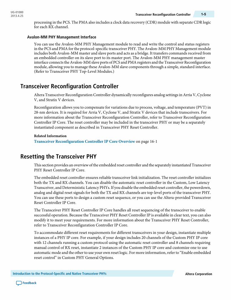
The following figure illustrates the top level modules that comprise the protocol-specific transceiver PHYIP cores. As illustrated, the Altera Transceiver Reconfiguration Controller IP Core is instantiated separately.
ISO9001:2008Registered
© 2013 Altera Corporation. All rights reserved. ALTERA, ARRIA, CYCLONE, HARDCOPY, MAX, MEGACORE, NIOS, QUARTUS and STRATIXwords and logos are trademarks of Altera Corporation and registered in the U.S. Patent and Trademark Office and in other countries. All other wordsand logos identified as trademarks or service marks are the property of their respective holders as described at www.altera.com/common/legal.html.Altera warrants performance of its semiconductor products to current specifications in accordance with Altera's standard warranty, but reserves theright to make changes to any products and services at any time without notice. Altera assumes no responsibility or liability arising out of the applicationor use of any information, product, or service described herein except as expressly agreed to in writing by Altera. Altera customers are advised toobtain the latest version of device specifications before relying on any published information and before placing orders for products or services.
www.altera.com
101 Innovation Drive, San Jose, CA 95134

Figure 1-1: Transceiver PHY Top-Level Modules
To MAC
To HSSI Pins
Transceiver PHY
PMAPCSCustomized functionality for:
10GBASE-R10GBASE-KR1G/10GBASE-R
XAUIInterlaken
PCI Express PIPE
Avalon-STTX and RX
Avalon-MMControl &Status
PCS & PMAControl & Status
Register Memory Map
SReset
Controller
S
Altera TransceiverReconfiguration
Controller
Offset CancellationAnalog Settings
Avalon-MM PHYManagement
Read & WriteControl & Status
Registers
M
Avalon-MM master interfaceM
S
Avalon-MM slave interfaceS
PLL CDR
Rx Deserializer
Tx Serializer
EmbeddedController
Related Information10GBASE-R PHY P Core on page 3-1
Backplane Ethernet 10GBASE-KR PHY IP Core Overview
1G/10 Gbps Ethernet PHY IP Core on page 5-1
XAUI PHY IP Core on page 6-1
Interlaken PHY IP Core on page 7-1
PHY IP Core for PCI Express (PIPE) on page 8-1
Native Transceiver PHYsEach device family, beginning with Series V devices offers a separate Native PHY IP core to provide low-levelaccess to the hardware. There are separate IP Cores for Arria V, Arria V GZ, Cyclone V, and Stratix Vdevices.
The Native PHYs allow you to customize the transceiver settings to meet your requirements. You can alsouse the Native PHYs to dynamically reconfigure the PCS datapath. Depending on protocol mode selected,built-in rules validate the options you specify. The following figure illustrates the Stratix V Native PHY.
Introduction to the Protocol-Specific and Native Transceiver PHYsAltera Corporation
Feedback
UG-01080Native Transceiver PHYs1-2 2013.4.25

Figure 1-2: Stratix V Transceiver Native PHY IP Core
PLLsPMA
altera_xcvr_native_<dev>Transceiver Native PHY
TransceiverReconfiguration
Controller
Reconfiguration to XCVR
Reconfiguration from XCVR
TX and RX Resets
Calilbration BusyPLL and RX Locked
RX PCS Parallel Data
TX PCS Parallel Data
CDR Reference Clock
(when neither PCS is enabled)
TX PLL Reference ClockSerializer/Clock
GenerationBlock
RX Serial Data
toFPGA fabric
TransceiverPHY ResetController
TX PMA Parallel DataRX PMA Parallel Data
TX Serial DataSerializer
Deserializer
StandardPCS
(optional)
10G PCS(optional)
As shown, the Stratix V Native PHY connects to the separately instantiated Transceiver ReconfigurationController and Transceiver PHY Reset Controller.
Table 1-1: Native Transceiver PHY Datapaths
Cyclone VArria V GZArria VStratix VDatapaths
-YesYesYesPMA Direct:
This datapath connects the FPGAfabric directly to the PMA,minimizing latency. You mustimplement any required PCSfunctions in the FPGA fabric.
YesYesYesYesStandard:
This datapath provides a completePCS and PMA for the TX and RXchannels. You can customize theStandard datapath by enabling ordisabling individual modules andspecifying data widths.
Altera CorporationIntroduction to the Protocol-Specific and Native Transceiver PHYs
Feedback
1-3Native Transceiver PHYsUG-010802013.4.25
Cyclone VArria V GZArria VStratix VDatapaths
-Yes-Yes10G:
This is a high performance datapath.It provides a complete PCS andPMAfor theTX andRX channels. You cancustomize the 10G datapath byenabling or disabling individualmodules and specifying datawidths.
Related InformationArria V Transceiver Native PHY IP Core on page 13-1
Arria V GZ Transceiver Native PHY IP Core on page 14-1
Cyclone V Transceiver Native PHY IP Core Overview on page 15-1
Stratix V Transceiver Native PHY IP Core on page 12-1
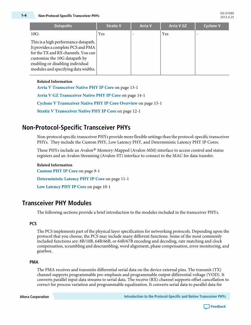
Non-Protocol-Specific Transceiver PHYsNon-protocol specific transceiver PHYs providemore flexible settings than the protocol-specific transceiverPHYs. They include the Custom PHY, Low Latency PHY, and Deterministic Latency PHY IP Cores.
These PHYs include an Avalon®Memory-Mapped (Avalon-MM) interface to access control and statusregisters and an Avalon Streaming (Avalon-ST) interface to connect to the MAC for data transfer.
Related InformationCustom PHY IP Core on page 9-1
Deterministic Latency PHY IP Core on page 11-1
Low Latency PHY IP Core on page 10-1
Transceiver PHY ModulesThe following sections provide a brief introduction to the modules included in the transceiver PHYs.
PCS
The PCS implements part of the physical layer specification for networking protocols. Depending upon theprotocol that you choose, the PCS may include many different functions. Some of the most commonlyincluded functions are: 8B/10B, 64B/66B, or 64B/67B encoding and decoding, rate matching and clockcompensation, scrambling and descrambling, word alignment, phase compensation, error monitoring, andgearbox.
PMA
The PMA receives and transmits differential serial data on the device external pins. The transmit (TX)channel supports programmable pre-emphasis and programmable output differential voltage (VOD). Itconverts parallel input data streams to serial data. The receive (RX) channel supports offset cancellation tocorrect for process variation and programmable equalization. It converts serial data to parallel data for
Introduction to the Protocol-Specific and Native Transceiver PHYsAltera Corporation
Feedback
UG-01080Non-Protocol-Specific Transceiver PHYs1-4 2013.4.25
processing in the PCS. The PMA also includes a clock data recovery (CDR) module with separate CDR logicfor each RX channel.
Avalon-MM PHY Management Interface
You can use the Avalon-MM PHY Management module to read and write the control and status registersin the PCS and PMA for the protocol-specific transceiver PHY. TheAvalon-MMPHYManagementmoduleincludes both Avalon-MM master and slave ports and acts as a bridge. It transfers commands received froman embedded controller on its slave port to its master port. The Avalon-MM PHY management masterinterface connects theAvalon-MMslave ports of PCS andPMAregisters and the Transceiver Reconfigurationmodule, allowing you to manage these Avalon-MM slave components through a simple, standard interface.(Refer to Transceiver PHY Top-Level Modules.)
Transceiver Reconfiguration ControllerAltera Transceiver ReconfigurationController dynamically reconfigures analog settings inArria V, CycloneV, and Stratix V devices.
Reconfiguration allows you to compensate for variations due to process, voltage, and temperature (PVT) in28-nm devices. It is required for Arria V, Cyclone V, and Stratix V devices that include transceivers. Formore information about the Transceiver Reconfiguration Controller, refer to Transceiver ReconfigurationController IP Core. The reset controller may be included in the transceiver PHY or may be a separatelyinstantiated component as described in Transceiver PHY Reset Controller.
Related InformationTransceiver Reconfiguration Controller IP Core Overview on page 16-1
Resetting the Transceiver PHYThis section provides an overview of the embedded reset controller and the separately instantiatedTransceiverPHY Reset Controller IP Core.
The embedded reset controller ensures reliable transceiver link initialization. The reset controller initializesboth the TX and RX channels. You can disable the automatic reset controller in the Custom, Low LatencyTransceiver, andDeterministic Latency PHYs. If you disable the embedded reset controller, the powerdown,analog and digital reset signals for both the TX and RX channels are top-level ports of the transceiver PHY.You can use these ports to design a custom reset sequence, or you can use the Altera-provided TransceiverReset Controller IP Core.
The Transceiver PHY Reset Controller IP Core handles all reset sequencing of the transceiver to enablesuccessful operation. Because the Transceiver PHY Reset Controller IP is available in clear text, you can alsomodify it to meet your requirements. For more information about the Transceiver PHY Reset Controller,refer to Transceiver Reconfiguration Controller IP Core.
To accommodate different reset requirements for different transceivers in your design, instantiate multipleinstances of a PHY IP core. For example, if your design includes 20 channels of the Custom PHY IP corewith 12 channels running a custom protocol using the automatic reset controller and 8 channels requiringmanual control of RX reset, instantiate 2 instances of the Custom PHY IP core and customize one to useautomaticmode and the other to use your own reset logic. Formore information, refer to “Enable embeddedreset control” in Custom PHY General Options.
Altera CorporationIntroduction to the Protocol-Specific and Native Transceiver PHYs
Feedback
1-5Transceiver Reconfiguration ControllerUG-010802013.4.25
For more information about reset control in Stratix V devices, refer to Transceiver Reset Control in StratixV Devices in volume 3 of the Stratix V Device Handbook. For Stratix IV devices, refer to Reset Control andPower Down in volume 4 of the Stratix IV Device Handbook. For Arria V devices, refer to Transceiver ResetControl and Power-Down in Arria V Devices. For Cyclone V devices refer to Transceiver Reset Control andPower Down in Cyclone V Devices.
Related InformationTransceiver Reset Control in Stratix V Devices
Reset Control and Power Down
Transceiver Reset Control and Power-Down in Arria V Devices
Transceiver Reset Control and Power Down in Cyclone V Devices
General Options Parameters on page 9-3
Transceiver PHY Reset Controller IP Core on page 17-1
Running a Simulation TestbenchWhen you generate your transceiver PHY IP core, the Quartus® II software generates the HDL files thatdefine your parameterized IP core. In addition, the Quartus II software generates an example Tcl script tocompile and simulate your design in ModelSim.
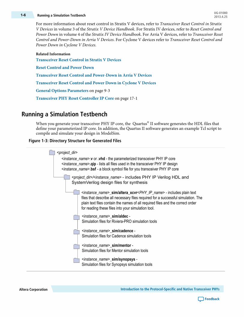
Figure 1-3: Directory Structure for Generated Files
<instance_name>_sim/synopsys -Simulation files for Synopsys simulation tools
<project_dir>
<project_dir>/<instance_name> - includes PHY IP Verilog HDL andSystemVerilog design files for synthesis
<instance_name>.v or .vhd - the parameterized transceiver PHY IP core<instance_name>.qip - lists all files used in the transceiver PHY IP design<instance_name>.bsf - a block symbol file for you transceiver PHY IP core
<instance_name>_sim/altera_xcvr<PHY_IP_name> - includes plain textfiles that describe all necessary files required for a successful simulation. Theplain text files contain the names of all required files and the correct orderfor reading these files into your simulation tool.
<instance_name>_sim/aldec -Simulation files for Riviera-PRO simulation tools
<instance_name>_sim/cadence -Simulation files for Cadence simulation tools
<instance_name>_sim/mentor -Simulation files for Mentor simulation tools
Introduction to the Protocol-Specific and Native Transceiver PHYsAltera Corporation
Feedback
UG-01080Running a Simulation Testbench1-6 2013.4.25

The following table describes the key files and directories for the parameterized transceiver PHY IP coreand the simulation environment which are in clear text.
Table 1-2: Transceiver PHY Files and Directories
DescriptionFile Name
The top-level project directory.<project_dir>
The top-level design file.<instance_name>.v or .vhd
A list of all files necessary for Quartus II compilation.<instance_name>.qip
A Block Symbol File (.bsf) for your transceiver PHY.<instance_name>.bsf
The directory that stores the HDL files that define theprotocol-specific PHY IP core. These files are used forsynthesis.
<project_dir>/<instance_name>/
Defines the transceiver. It includes instantiations of thePCS and PMA modules and Avalon-MM PHYmanagement interface.
sv_xcvr_native.sv
These files perform rule based checking for the modulespecified. For example, if the PLL type, data rate, andFPGA fabric transceiver interface width are notcompatible, the checker reports an error.
stratixv_hssi_<module_name>_rbc.sv
Generates waitrequest for protocol-specific transceiverPHY IP core that includes backpressure.
altera_wait_generate.v
Includes the reset controller logic.alt_reset_ctrl_tgx_cdrauto.sv
Includes an example of the PLL_TYPE assignmentstatement required to specify the PLL type for each PLLin the design. The available types are clock multiplierunit (CMU) and auxiliary transmit (ATX).
<instance_name>_phy_assignments.qip
<project_dir>/<instance_name>_sim/altera_xcvr_<PHY_IP_name>/
The simulation directory.
Simulation files for Riviera-PRO simulation tools.<project_dir>/<instance_name>_sim/aldec
Simulation files for Cadence simulation tools.<project_dir>/<instance_name>_sim/cadence
Simulation files for Mentor simulation tools.<project_dir>/<instance_name>_sim/mentor
Simulation files for Synopsys simulation tools.<project_dir>/<instance_name>_sim/synopsys
The Verilog and VHDL transceiver PHY IP cores have been tested with the following simulators:
• ModelSim SE• Synopsys VCS MX• Cadence NCSim
If you select VHDL for your transceiver PHY, only the wrapper generated by the Quartus II software is inVHDL. All the underlying files are written in Verilog or System Verilog. To enable simulation using a
Altera CorporationIntroduction to the Protocol-Specific and Native Transceiver PHYs
Feedback
1-7Running a Simulation TestbenchUG-010802013.4.25

VHDL-only ModelSim license, the underlying Verilog and System Verilog files for the transceiver PHY areencrypted so that they can be used with the top-level VHDL wrapper without using a mixed-languagesimulator.
For more information about simulating with ModelSim, refer to the Mentor Graphics ModelSim Supportchapter in volume 3 of the Quartus II Handbook.
The transceiver PHY IP cores do not support the NativeLink feature in the Quartus II software.
Related InformationMentor Graphics ModelSim Support
Unsupported FeaturesThe protocol-specific and native transceiver PHYs are not supported in Qsys in the current release.
Introduction to the Protocol-Specific and Native Transceiver PHYsAltera Corporation
Feedback
UG-01080Unsupported Features1-8 2013.4.25
2Getting Started Overview
2013.4.25UG-01080 Subscribe Feedback
This chapter provides a general overview of the Altera IP core design flow to help you quickly get startedwith any Altera IP core.
TheAltera IP Library is installed as part of theQuartus II installation process. You can select and parameterizeany Altera IP core from the library. Altera provides an integrated parameter editor that allows you tocustomize IP cores to support a wide variety of applications. The parameter editor guides you through thesetting of parameter values and selection of optional ports. The following sections describe the general designflow and use of Altera IP cores.
Installation and Licensing of IP CoresThe Altera IP Library is distributed with the Quartus II software and downloadable from the Altera website.
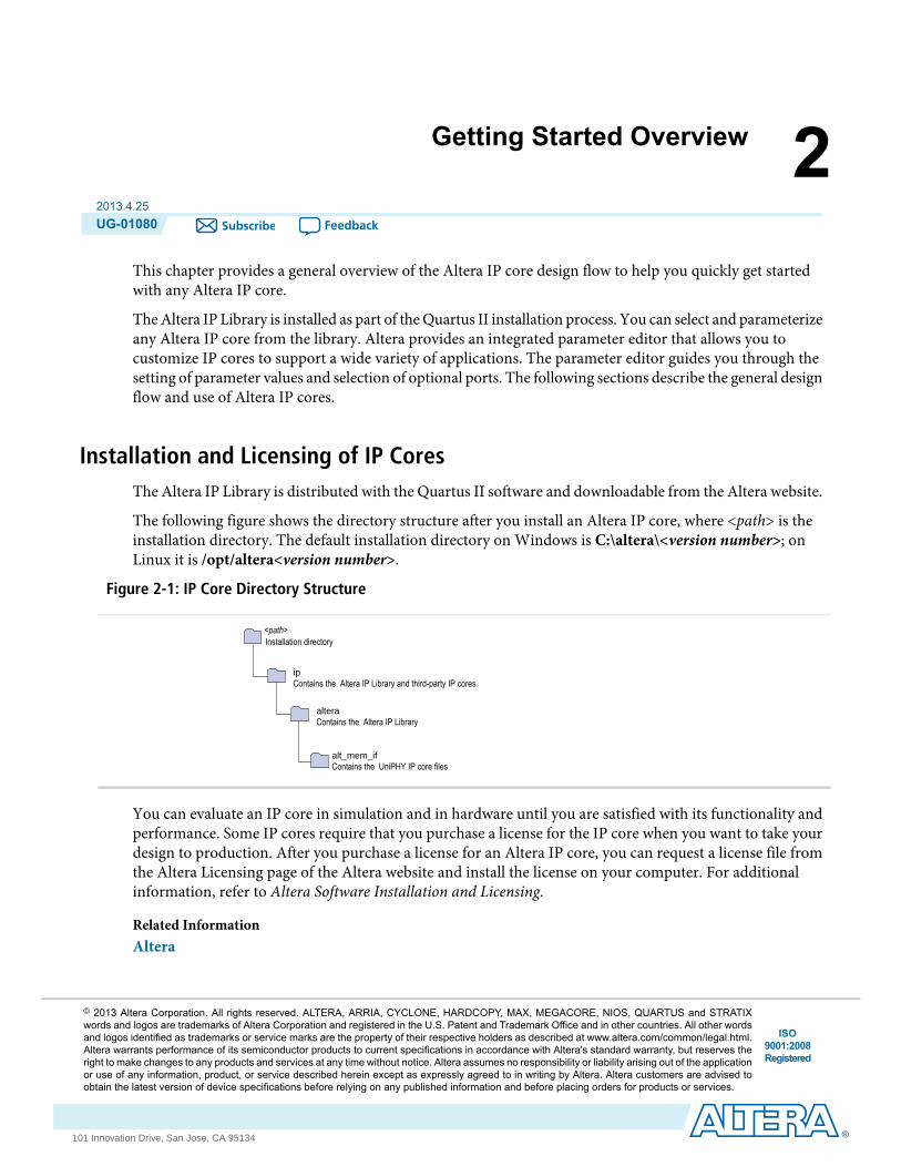
The following figure shows the directory structure after you install an Altera IP core, where <path> is theinstallation directory. The default installation directory on Windows is C:\altera\<version number>; onLinux it is /opt/altera<version number>.
Figure 2-1: IP Core Directory Structure
<path>Installation directory
ipContains the Altera IP Library and third-party IP cores
alteraContains the Altera IP Library
alt_mem_ifContains the UniPHY IP core files
You can evaluate an IP core in simulation and in hardware until you are satisfied with its functionality andperformance. Some IP cores require that you purchase a license for the IP core when you want to take yourdesign to production. After you purchase a license for an Altera IP core, you can request a license file fromthe Altera Licensing page of the Altera website and install the license on your computer. For additionalinformation, refer to Altera Software Installation and Licensing.
Related InformationAltera
ISO9001:2008Registered
© 2013 Altera Corporation. All rights reserved. ALTERA, ARRIA, CYCLONE, HARDCOPY, MAX, MEGACORE, NIOS, QUARTUS and STRATIXwords and logos are trademarks of Altera Corporation and registered in the U.S. Patent and Trademark Office and in other countries. All other wordsand logos identified as trademarks or service marks are the property of their respective holders as described at www.altera.com/common/legal.html.Altera warrants performance of its semiconductor products to current specifications in accordance with Altera's standard warranty, but reserves theright to make changes to any products and services at any time without notice. Altera assumes no responsibility or liability arising out of the applicationor use of any information, product, or service described herein except as expressly agreed to in writing by Altera. Altera customers are advised toobtain the latest version of device specifications before relying on any published information and before placing orders for products or services.
www.altera.com
101 Innovation Drive, San Jose, CA 95134

Altera Licensing
Altera Software Installation and Licensing
Design FlowsThis section describes how to parameterize Altera IP cores.
You can use the following flow(s) to parameterize Altera IP cores:
• MegaWizardTM™ Plug-In Manager Flow
Figure 2-2: Design Flows
1
Select Design Flow
Specify Parameters
Qsys orSOPC Builder
FlowMegaWizardFlow
Complete Qsys orSOPC Builder System
Specify Parameters
IP Complete
PerformFunctional Simulation
Debug Design
DoesSimulation GiveExpected Results?
Yes
Optional
Add Constraintsand Compile Design
The MegaWizard Plug-In Manager flow offers the following advantages:
• Allows you to parameterize an IP core variant and instantiate into an existing design• For some IP cores, this flow generates a complete example design and testbench
MegaWizard Plug-In Manager FlowThis section describes how to specify parameters and simulate your IP core with the MegaWizard Plug-InManager.
1 Altera IP cores may or may not support the Qsys and SOPC Builder design flows.
Getting Started OverviewAltera Corporation
Feedback
UG-01080Design Flows2-2 2013.4.25
The MegaWizard™ Plug-In Manager flow allows you to customize your IP core and manually integrate thefunction into your design.
Specifying ParametersTo specify IP core parameters with the MegaWizard Plug-In Manager, follow these steps:
1. Create a Quartus II project using the New Project Wizard available from the File menu.2. In the Quartus II software, launch the MegaWizard Plug-in Manager from the Tools menu, and follow
the prompts in the MegaWizard Plug-In Manager interface to create or edit a custom IP core variation.3. To select a specific Altera IP core, click the IP core in the Installed Plug Ins list in the MegaWizard Plug
In Manager.4. Specify the parameters on the Parameter Settings pages. For detailed explanations of these parameters,
refer to the "Parameter Settings" chapter in this document or the "Documentation" button in theMegaWizard parameter editor.
Some IP cores provide preset parameters for specific applications. If you wish to use presetparameters, click the arrow to expand the Presets list, select the desired preset, and then click
Note:
Apply. To modify preset settings, in a text editor modify the <installation directory>/ip/altera/alt_mem_if_interfaces/alt_mem_if_<memory_protocol>_emif/alt_mem_if_<memory_protocol>_mem_model.qprs file.
5. If the IP core provides a simulation model, specify appropriate options in the wizard to generate asimulation model.
Altera IP supports a variety of simulation models, including simulation-specific IP functionalsimulation models and encrypted RTL models, and plain text RTL models. These are all
Note:
cycle-accurate models. The models allow for fast functional simulation of your IP core instanceusing industry-standard VHDL or Verilog HDL simulators. For some cores, only the plain textRTL model is generated, and you can simulate that model.
Formore information about functional simulationmodels for Altera IP cores, refer to SimulatingAltera Designs in volume 3 of the Quartus II Handbook.
Note:
Use the simulation models only for simulation and not for synthesis or any other purposes.Using these models for synthesis creates a nonfunctional design.
Caution:
6. If the parameter editor includes EDA and Summary tabs, follow these steps:a. Some third-party synthesis tools can use a netlist that contains the structure of an IP core but no
detailed logic to optimize timing and performance of the design containing it. To use this feature ifyour synthesis tool and IP core support it, turn on Generate netlist.
b. On the Summary tab, if available, select the files you want to generate. A gray checkmark indicates afile that is automatically generated. All other files are optional.
If file selection is supported for your IP core, after you generate the core, a generation report(<variation name>.html)appears in your project directory. This file contains informationabout the generated files.
Note:
7. Click the Finish button, the parameter editor generates the top-level HDL code for your IP core, and asimulation directory which includes files for simulation.
Altera CorporationGetting Started Overview
Feedback
2-3Specifying ParametersUG-010802013.4.25

Note: The Finish button may be unavailable until all parameterization errors listed in the messageswindow are corrected.
8. Click Yes if you are prompted to add the Quartus II IP File (.qip) to the current Quartus II project. Youcan also turn on Automatically add Quartus II IP Files to all projects.
You can now integrate your custom IP core instance in your design, simulate, and compile.While integratingyour IP core instance into your design, you must make appropriate pin assignments. You can create a virtualpin to avoid making specific pin assignments for top-level signals while you are simulating and not readyto map the design to hardware.
For some IP cores, the generation process also creates complete example designs. An example design forhardware testing is located in the < variation_name > _example_design/example_project/ directory. Anexample design for RTL simulation is located in the < variation_name > _example_design/simulation/directory.
For information about the Quartus II software, including virtual pins and the MegaWizard Plug-InManager, refer to Quartus II Help.
Note:
Related InformationSimulating Altera Designs
Quartus II Help
Simulate the IP CoreThis section describes how to simulate your IP core.
You can simulate your IP core variation with the functional simulation model and the testbench or exampledesign generated with your IP core. The functional simulation model and testbench files are generated in aproject subdirectory. This directory may also include scripts to compile and run the testbench.
For a complete list of models or libraries required to simulate your IP core, refer to the scripts provided withthe testbench.
For more information about simulating Altera IP cores, refer to Simulating Altera Designs in volume 3 ofthe Quartus II Handbook.
Related InformationSimulating Altera Designs
Getting Started OverviewAltera Corporation
Feedback
UG-01080Simulate the IP Core2-4 2013.4.25

310GBASE-R PHY P Core
2013.4.25UG-01080 Subscribe Feedback
TheAltera 10GBASE-R PHY IPCore implements the functionality described in IEEE Standard 802.3 Clause45.
It delivers serialized data to an optical module that drives optical fiber at a line rate of 10.3125 gigabits persecond (Gbps). In a multi-channel implementation of 10GBASE-R, each channel of the 10GBASE-R PHYIP Core operates independently. Both the PCS and PMA of the 10GBASE-R PHY are implemented as hardIP blocks in Stratix V devices, saving FPGA resources.
Figure 3-1: 10GBASE-R PHY with Hard PCS with PMA in Stratix V Devices
10GBASE-R PHY IP Core
10.3125 Gbps serialXFI/SFP+
Stratix V FPGA
PMA
Hard PCS10GBASE-R
64b/66bScramblerGearbox
SDR XGMII72 bits @ 156.25 Mbps
Avalon-MMControl & Status
TransceiverReconfiguraiton
For a 10-Gbps Ethernet solution that includes both the Ethernet MAC and the 10GBASE-R PHY,refer to the 10-Gbps Ethernet MAC MegaCore Function User Guide.
Note:
For more detailed information about the 10GBASE-R transceiver channel datapath, clocking, andchannel placement, refer to the “10GBASE-R” section in the Transceiver Configurations in Stratix VDevices chapter of the Stratix V Device Handbook.
Note:
The following figure illustrates a multiple 10 GbE channel IP core in a Stratix IV GT device. To achievehigher bandwidths, you can instantiate multiple channels. The PCS is available in soft logic for Stratix IVGT devices; it connects to a separately instantiated hard PMA. The PCS connects to an Ethernet MAC viasingle data rate (SDR) XGMII running at 156.25 megabits per second (Mbps) and transmits data to a 10Gbps transceiver PMA running at 10.3125 Gbps in a Stratix IV GT device.
To make the most effective use of this soft PCS and PMA configuration for Stratix IV GT devices, you cangroup up to four channels in a single quad and control their functionality using one Avalon-MM PHYmanagement bridge, transceiver reconfiguration module, and low controller. As this figure illustrates, the
ISO9001:2008Registered
© 2013 Altera Corporation. All rights reserved. ALTERA, ARRIA, CYCLONE, HARDCOPY, MAX, MEGACORE, NIOS, QUARTUS and STRATIXwords and logos are trademarks of Altera Corporation and registered in the U.S. Patent and Trademark Office and in other countries. All other wordsand logos identified as trademarks or service marks are the property of their respective holders as described at www.altera.com/common/legal.html.Altera warrants performance of its semiconductor products to current specifications in accordance with Altera's standard warranty, but reserves theright to make changes to any products and services at any time without notice. Altera assumes no responsibility or liability arising out of the applicationor use of any information, product, or service described herein except as expressly agreed to in writing by Altera. Altera customers are advised toobtain the latest version of device specifications before relying on any published information and before placing orders for products or services.
www.altera.com
101 Innovation Drive, San Jose, CA 95134
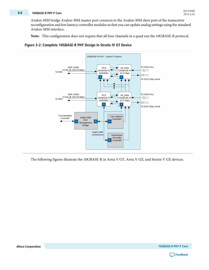
Avalon-MM bridge Avalon-MM master port connects to the Avalon-MM slave port of the transceiverreconfiguration and low latency controllermodules so that you can update analog settings using the standardAvalon-MM interface.
This configuration does not require that all four channels in a quad run the 10GBASE-R protocol.Note:
Figure 3-2: Complete 10GBASE-R PHY Design in Stratix IV GT Device
To MAC
To EmbeddedController
Avalon-MMconnections
10GBASE-R PHY - Stratix IV Device
SDR XGMII72 bits @ 156.25 Mbps
To MAC
SDR XGMII72 bits @ 156.25 Mbps
Avalon-MMPHY
ManagementBridge
MS S
Low LatencyController
S
TransceiverReconfigController
Alt_PMA10GBASE-R10.3 Gbps
10.3125 Gbps serial
To HSSI PinsPCS10GBASE-R
(64b/66b)
S S
Alt_PMA10GBASE-R10.3 Gbps
10.3125 Gbps serial
To HSSI PinsPCS10GBASE-R
(64b/66b)
S S
The following figures illustrate the 10GBASE-R in Arria V GT, Arria V GZ, and Stratix V GX devices.
10GBASE-R PHY P CoreAltera Corporation
Feedback
UG-0108010GBASE-R PHY P Core3-2 2013.4.25
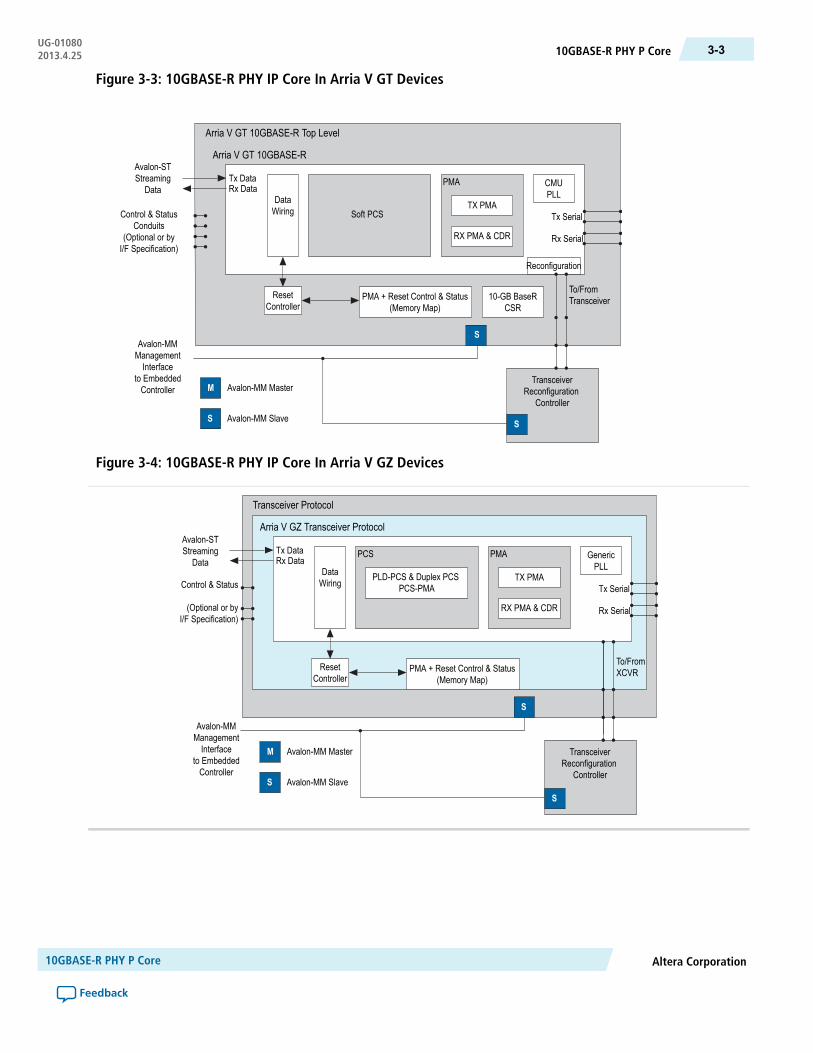
Figure 3-3: 10GBASE-R PHY IP Core In Arria V GT Devices
TransceiverReconfiguration
Controller
DataWiring Soft PCS
TX PMA
PMA
RX PMA & CDR
CMUPLL
ResetController
Avalon-MM Slave
Avalon-MM Master
PMA + Reset Control & Status(Memory Map)
10-GB BaseRCSR
Tx Serial
Rx Serial
Reconfiguration
Avalon-MMManagementInterface
to EmbeddedController
Control & StatusConduits
(Optional or byI/F Specification)
Avalon-STStreaming
DataTx DataRx Data
Arria V GT 10GBASE-R Top Level
Arria V GT 10GBASE-R
To/FromTransceiver
S
M
S
S
Figure 3-4: 10GBASE-R PHY IP Core In Arria V GZ Devices
DataWiring PLD-PCS & Duplex PCS
PCS-PMA
PCS
TX PMA
PMA
RX PMA & CDR
GenericPLL
ResetController
TransceiverReconfiguration
Controller
S
PMA + Reset Control & Status(Memory Map)
Tx Serial
Rx Serial
S
Control & Status
(Optional or byI/F Specification)
Avalon-STStreaming
DataTx DataRx Data
Transceiver Protocol
Arria V GZ Transceiver Protocol
To/FromXCVR
Avalon-MM Slave
Avalon-MM Master
S
M
Avalon-MMManagementInterface
to EmbeddedController
Altera Corporation10GBASE-R PHY P Core
Feedback
3-310GBASE-R PHY P CoreUG-010802013.4.25
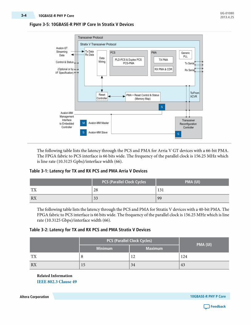
Figure 3-5: 10GBASE-R PHY IP Core In Stratix V Devices
DataWiring PLD-PCS & Duplex PCS
PCS-PMA
PCS
TX PMA
PMA
RX PMA & CDR
GenericPLL
ResetController
PMA + Reset Control & Status(Memory Map)
Tx Serial
Rx Serial
S
Control & Status
(Optional or byI/F Specification)
Avalon-STStreaming
DataTx DataRx Data
Transceiver Protocol
Stratix V Transceiver Protocol
To/FromXCVR
Avalon-MM Slave
Avalon-MM Master
S
M
Avalon-MMManagementInterface
to EmbeddedController
TransceiverReconfiguration
Controller
S
The following table lists the latency through the PCS and PMA for Arria V GT devices with a 66-bit PMA.The FPGA fabric to PCS interface is 66 bits wide. The frequency of the parallel clock is 156.25 MHz whichis line rate (10.3125 Gpbs)/interface width (66).
Table 3-1: Latency for TX and RX PCS and PMA Arria V Devices
PMA (UI)PCS (Parallel Clock Cycles
13128TX
9933RX
The following table lists the latency through the PCS and PMA for Stratix V devices with a 40-bit PMA. TheFPGA fabric to PCS interface is 66 bits wide. The frequency of the parallel clock is 156.25 MHz which is linerate (10.3125 Gbps)/interface width (66).
Table 3-2: Latency for TX and RX PCS and PMA Stratix V Devices
PMA (UI)PCS (Parallel Clock Cycles)
MaximumMinimum
124128TX
433415RX
Related InformationIEEE 802.3 Clause 49
10GBASE-R PHY P CoreAltera Corporation
Feedback
UG-0108010GBASE-R PHY P Core3-4 2013.4.25

10-Gbps Ethernet MAC MegaCore Function User Guide
Transceiver Configurations in Stratix V Devices
10GBASE-R PHY Release InformationRelease information for the IP core.
Table 3-3: 10GBASE-R Release Information
DescriptionItem
12.1Version
Nov-12Release Date
IP-10GBASERPCS (primary) IPR-10GBASERPCS(renewal)
Ordering Codes2
00D7Product ID
6AF7Vendor ID
10GBASE-R PHY Device Family SupportDevice support for the IP core.
IP cores provide either final or preliminary support for target Altera device families. These terms have thefollowing definitions:
• Final support—Verified with final timing models for this device.• Preliminary support—Verified with preliminary timing models for this device.
Table 3-4: Device Family Support
SupportDevice Family
PreliminaryArria V GT devices–Soft PCS and Hard PMA
PreliminaryArria V GZ
FinalStratix IV GT devices–Soft PCS and Hard PMA
PreliminaryStratix V devices–Hard PCS and PMA
No supportOther device families
For speed grade information, refer to “Transceiver Performance Specifications” in the DC andSwitching Characteristics chapter in the Stratix IVHandbook for Stratix IV devices or Stratix VDeviceDatasheet.
Note:
2 No ordering codes or license files are required for Stratix V devices.
Altera Corporation10GBASE-R PHY P Core
Feedback
3-510GBASE-R PHY Release InformationUG-010802013.4.25

Related InformationDC and Switching Characteristics
Stratix V Device Datasheet.
10GBASE-R PHY Performance and Resource Utilization for Stratix IV DevicesBecause the 10GBASE-R PHY is implemented in hard logic it uses less than 1% of the available ALMs,memory, primary and secondary logic registers. The following table lists the typical expected device resourceutilization for duplex channels using the current version of the Quartus II software targeting a Stratix IVGT device. The numbers of combinational ALUTs, logic registers, and memory bits are rounded to thenearest 100.
Table 3-5: 10GBASE-R PHY Performance and Resource Utilization—Stratix IV GT Device
Memory BitsLogic Registers (Bits)Combinational ALUTsChannels
4700410052001
188001300156004
47500321003810010
10GBASE-R PHY Performance and Resource Utilization for Arria V GT DevicesThe following table lists the resource utilization when targeting an Arria V (5AGTFD7K3F4015) device.Resource utilization numbers reflect changes to the resource utilization reporting starting in the Quartus IIsoftware v12.1 release for 28 nm device families and upcoming device families. The numbers of ALMs andlogic registers are rounded up to the nearest 100.
For information about Quartus II resource utilization reporting, refer to Fitter Resources Reports inthe Quartus II Help.
Note:
Table 3-6: 10GBASE-R PHY Performance and Resource Utilization—Arria V GT Device
Memory 10KSecondary Logic RegistersPrimary Logic RegistersALMsChannels
7300300028001
Related InformationFitter Resources Reports
10GBASE-R PHY Performance and Resource Utilization for Arria V GZ andStratix V Devices
Because the 10GBASE-R PHY is implemented in hard logic in Arria V GZ and Stratix V devices, it uses lessthan 1% of the available ALMs, memory, primary and secondary logic registers.
The following table lists the total latency for an Ethernet packet with a 9600 byte payload and an inter-packetgap of 12 characters. The latency includes the number of cycles to transmit the payload from the TX XGMII
10GBASE-R PHY P CoreAltera Corporation
Feedback
UG-0108010GBASE-R PHY Performance and Resource Utilization for Stratix IV Devices3-6 2013.4.25

interface, through the TX PCS and PMA, looping back through the RX PMA and PCS to the RX XGMIIinterface. (Stratix V Clock Generation and Distribution illustrates this datapath.)
Table 3-7: Latency
CyclesPPM Difference
350 PPM
35-200 PPM
42+200 PPM
If latency is critical, Altera recommends designing your own soft 10GBASE-R PCS and connectingto the Low Latency PHY IP Core.
Note:
Parameterizing the 10GBASE-R PHYThe 10GBASE-R PHY IP Core is available for the Arria V, Arria V GZ, Stratix IV, or Stratix V devicefamilies. Complete the following steps to configure the 10GBASE-R PHY IPCore in theMegaWizard Plug-InManager:
1. For Which device family will you be using?, select Arria V, Arria V GZ, Stratix IV, or Stratix V fromthe list.
2. Click Installed Plug-Ins > Interfaces > Ethernet> 10GBASE-R PHY v12.1.3. Use the tabs on the MegaWizard Plug-In Manager to select the options required for the protocol.4. Refer to the following topics to learn more about the parameters:
a. General Option Parameters on page 3-7b. 10GBASE-R PHY Analog Parameters
5. Click Finish to generate your parameterized 10GBASE-R PHY IP Core.
General Option ParametersThis section describes general parameters.
This section describes the 10GBASE-R PHY parameters, which you can set using the MegaWizard Plug-InManager.
Table 3-8: General Options
DescriptionValueName
General Options
Specifies the target device.Arria V
Arria V GZ
Stratix IV GT
Stratix V
Device family
Altera Corporation10GBASE-R PHY P Core
Feedback
3-7Parameterizing the 10GBASE-R PHYUG-010802013.4.25
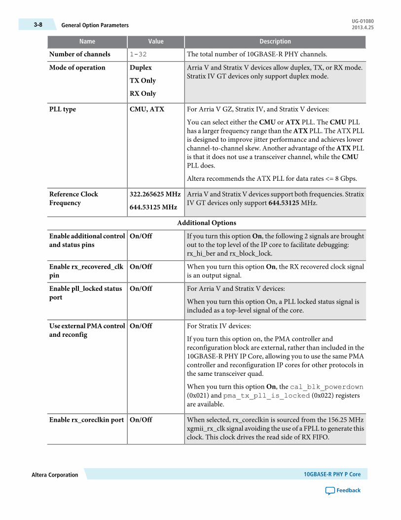
DescriptionValueName
The total number of 10GBASE-R PHY channels.1-32Number of channels
Arria V and Stratix V devices allow duplex, TX, or RX mode.Stratix IV GT devices only support duplex mode.
Duplex
TX Only
RX Only
Mode of operation
For Arria V GZ, Stratix IV, and Stratix V devices:
You can select either the CMU or ATX PLL. The CMU PLLhas a larger frequency range than theATX PLL. The ATX PLLis designed to improve jitter performance and achieves lowerchannel-to-channel skew. Another advantage of the ATX PLLis that it does not use a transceiver channel, while the CMUPLL does.
Altera recommends the ATX PLL for data rates <= 8 Gbps.
CMU, ATXPLL type
Arria V and Stratix V devices support both frequencies. StratixIV GT devices only support 644.53125 MHz.
322.265625 MHz
644.53125 MHz
Reference ClockFrequency
Additional Options
If you turn this option On, the following 2 signals are broughtout to the top level of the IP core to facilitate debugging:rx_hi_ber and rx_block_lock.
On/OffEnable additional controland status pins
When you turn this option On, the RX recovered clock signalis an output signal.
On/OffEnable rx_recovered_clkpin
For Arria V and Stratix V devices:
When you turn this option On, a PLL locked status signal isincluded as a top-level signal of the core.
On/OffEnable pll_locked statusport
For Stratix IV devices:
If you turn this option on, the PMA controller andreconfiguration block are external, rather than included in the10GBASE-R PHY IP Core, allowing you to use the same PMAcontroller and reconfiguration IP cores for other protocols inthe same transceiver quad.
When you turn this option On, the cal_blk_powerdown(0x021) and pma_tx_pll_is_locked (0x022) registersare available.
On/OffUse external PMAcontroland reconfig
When selected, rx_coreclkin is sourced from the 156.25 MHzxgmii_rx_clk signal avoiding the use of a FPLL to generate thisclock. This clock drives the read side of RX FIFO.
On/OffEnable rx_coreclkin port
10GBASE-R PHY P CoreAltera Corporation
Feedback
UG-01080General Option Parameters3-8 2013.4.25
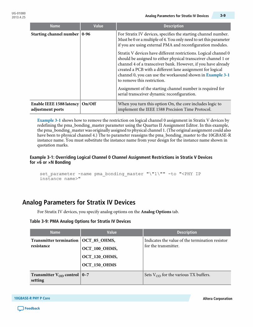
DescriptionValueName
For Stratix IV devices, specifies the starting channel number.Must be 0 or amultiple of 4. You only need to set this parameterif you are using external PMA and reconfiguration modules.
Stratix V devices have different restrictions. Logical channel 0should be assigned to either physical transceiver channel 1 orchannel 4 of a transceiver bank. However, if you have alreadycreated a PCB with a different lane assignment for logicalchannel 0, you can use the workaound shown in Example 3-1to remove this restriction.
Assignment of the starting channel number is required forserial transceiver dynamic reconfiguration.
0-96Starting channel number
When you turn this option On, the core includes logic toimplement the IEEE 1588 Precision Time Protocol.
On/OffEnable IEEE 1588 latencyadjustment ports
Example 3-1 shows how to remove the restriction on logical channel 0 assignment in Stratix V devices byredefining the pma_bonding_master parameter using the Quartus II Assignment Editor. In this example,the pma_bonding_master was originally assigned to physical channel 1. (The original assignment could alsohave been to physical channel 4.) The to parameter reassigns the pma_bonding_master to the 10GBASE-Rinstance name. You must substitute the instance name from your design for the instance name shown inquotation marks.
Example 3-1: Overriding Logical Channel 0 Channel Assignment Restrictions in Stratix V Devicesfor ×6 or ×N Bonding
set_parameter -name pma_bonding_master "\"1\"" -to "<PHY IPinstance name>"
Analog Parameters for Stratix IV DevicesFor Stratix IV devices, you specify analog options on the Analog Options tab.
Table 3-9: PMA Analog Options for Stratix IV Devices
DescriptionValueName
Indicates the value of the termination resistorfor the transmitter.
OCT_85_OHMS,
OCT_100_OHMS,
OCT_120_OHMS,
OCT_150_OHMS
Transmitter terminationresistance
Sets VOD for the various TX buffers.0–7Transmitter VOD controlsetting
Altera Corporation10GBASE-R PHY P Core
Feedback
3-9Analog Parameters for Stratix IV DevicesUG-010802013.4.25

DescriptionValueName
Sets the amount of pre-emphasis on the TXbuffer.
0–7Pre-emphasis pre-tapsetting
Determines whether or not the pre-emphasiscontrol signal for the pre-tap is inverted. If youturn this option on, the pre-emphasis controlsignal is inverted.
On, OffInvert the pre-emphasispre-tap polarity setting
Sets the amount of pre-emphasis for the 1stpost-tap.
0-15Pre-emphasis firstpost-tap setting
Sets the amount of pre-emphasis for the 2ndpost-tap.
0–7Pre-emphasis secondpost-tap setting
Determines whether or not the pre-emphasiscontrol signal for the second post-tap is inverted.If you turn this option on, the pre-emphasiscontrol signa is inverted.
On, OffInvert the pre-emphasissecond post-tap polarity
Specifies the RX common mode voltage.Tri-State
0.82V
1.1v
Receiver common modevoltage
Indicates the value of the termination resistorfor the receiver.
OCT_85_OHMS
OCT_100_OHMs
OCT_120_OHMS
OCT_150_OHMS
Receiver terminationresistance
Sets the equalization DC gain using one of thefollowing settings:
• 0: 0 dB• 1: 3 dB• 2: 6 dB• 3: 9 dB• 4: 12 dB
0-4Receiver DC
This option sets the equalizer control settings.The equalizer uses a pass band filter. Specifyinga low value passes low frequencies. Specifyinga high value passes high frequencies.
0-15Receiver static equalizersetting:
Analog Parameters for Arria V, Arria V GZ, and Stratix V DevicesClick on the appropriate links to review the analog parameters for these devices.
10GBASE-R PHY P CoreAltera Corporation
Feedback
UG-01080Analog Parameters for Stratix IV Devices3-10 2013.4.25

Related InformationAnalog Settings for Arria V Devices on page 19-2
Analog Settings for Arria V GZ Devices on page 19-9
Analog Settings for Stratix V Devices on page 19-25
10GBASE-R PHY InterfacesThis section describes the 10GBASE-R PHY interfaces.
The following figure illustrates the top-level signals of the 10BASE-R PHY; <n> is the channel number.
Figure 3-6: 10GBASE-R PHY Top-Level Signals
xgmii_tx_dc<n> [71:0]tx_readyxgmii_tx_clk
xgmii_rx_dc<n> [71:0]rx_readyrx_data_ready[<n> -1:0]xgmii_rx_clkrx_coreclkin
phy_mgmt_clkphy_mgmt_clk_resetphy_mgmt_addr[8:0]phy_mgmt_writedata[31:0]phy_mgmt_readdata[31:0]phy_mgmt_writephy_mgmt_readphy_mgmt_waitrequest
10GBASE-R Top-Level Signals
DynamicReconfiguration
ExternalPMA Control
Stratix IVDevices
rx_serial_data<n>tx_serial_data<n>
gxb_pdnpll_pdn
cal_blk_pdncal_blk_clkpll_locked
reconfig_to_xcvr[3:0]reconfig_from_xcvr[<n> /4)17-1:0]
reconfig_to_xcvr[(<n> 70-1):0]reconfig_from_xcvr[(<n> 46-1):0]
rx_block_lockrx_hi_ber
rx_recovered_clk[<n> ]rx_latency_adj<n> [11:0]tx_latency_adj<n> [11:0]
pll_ref_clk
TransceiverSerial DataSDR XGMII TX
Inputs from MAC
SDR XGMII RXOutputs from PCS
towards MAC
Avalon-MM PHYManagement
Interface Status, 1588and Reference`
Clock
The block diagram shown in the GUI labels the external pins with the interface type and places theinterface name inside the box. The interface type and name are used in the Hardware Component
Note:
Description File (_hw.tcl). If you turn on Show signals, the block diagram displays all top-levelsignal names.
For more information about _hw.tcl files refer to refer to the Component Interface Tcl Reference chapter involume 1 of the Quartus II Handbook.
Related InformationComponent Interface Tcl Reference
10GBASE-R PHY Data InterfacesThis section describes the 10GBASE-R PHY data interfaces.
The TX signals are driven from the MAC to the PCS. The RX signals are driven from the PCS to the MAC.
Altera Corporation10GBASE-R PHY P Core
Feedback
3-1110GBASE-R PHY InterfacesUG-010802013.4.25

Table 3-10: SDR XGMII TX Inputs
DescriptionDirectionSignal Name
XGMII TX Interface
Contains 8 lanes of data and control forXGMII. Each lane consists of 8 bits of dataand 1 bit of control.
• Lane 0-[7:0]/[8]• Lane 1-[16:9]/[17]• Lane 2-[25:18]/[26]• Lane 3-[34:27]/[35]• Lane 4-[43:36]/[44]• Lane 5-[52:45]/[53]• Lane 6-[61:54]/[62]• Lane 7-[70:63]/[71]
Refer toTable 3-11 for the mapping of thexgmii_tx_dc data and control to thexgmii_sdr_dataandxgmii_sdr_ctrlsignals.
Inputxgmii_tx_dc_[<n>71:0]
Asserted when the TX channel is ready totransmit data. Because the readyLatencyon this Avalon-ST interface is 0, the MACmay drivetx_ready as soon as it comes outof reset.
Outputtx_ready
The XGMII TX clock which runs at 156.25MHz.Connectxgmii_tx_clk toxgmii_rx_clk to guarantee this clock is within 150ppm of the transceiver reference clock.
Inputxgmii_tx_clk
XGMII RX Interface
10GBASE-R PHY P CoreAltera Corporation
Feedback
UG-0108010GBASE-R PHY Data Interfaces3-12 2013.4.25
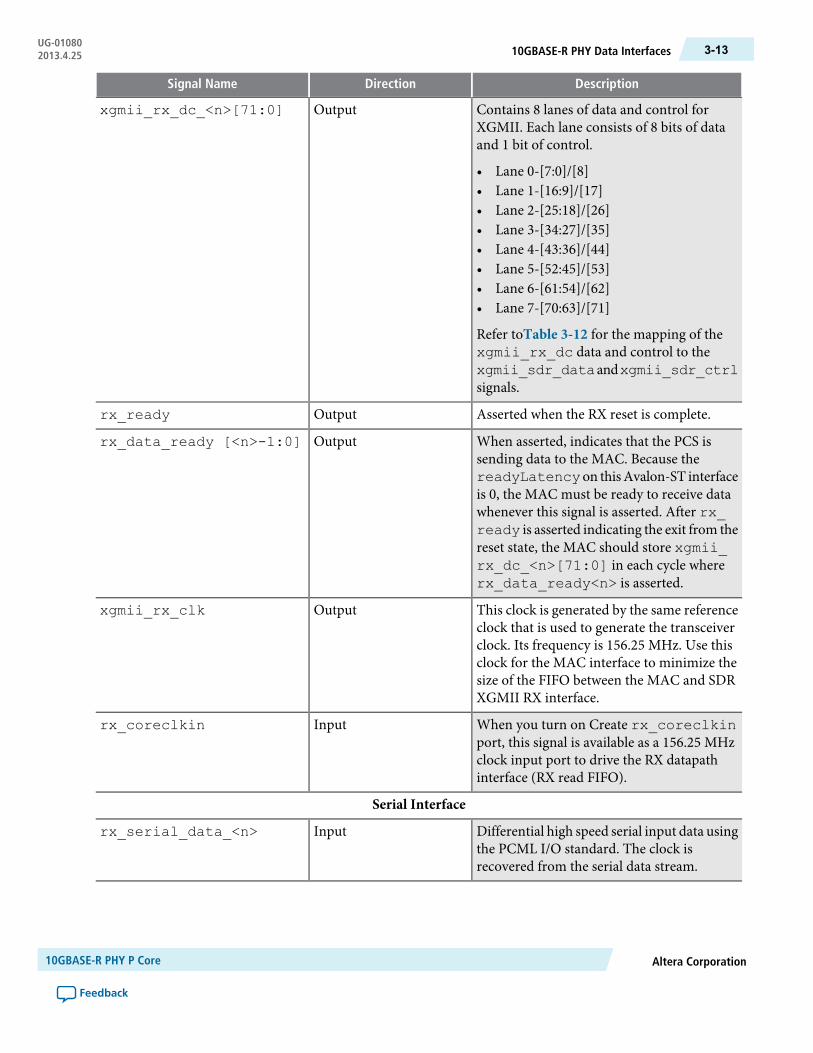
DescriptionDirectionSignal Name
Contains 8 lanes of data and control forXGMII. Each lane consists of 8 bits of dataand 1 bit of control.
• Lane 0-[7:0]/[8]• Lane 1-[16:9]/[17]• Lane 2-[25:18]/[26]• Lane 3-[34:27]/[35]• Lane 4-[43:36]/[44]• Lane 5-[52:45]/[53]• Lane 6-[61:54]/[62]• Lane 7-[70:63]/[71]
Refer toTable 3-12 for the mapping of thexgmii_rx_dc data and control to thexgmii_sdr_dataandxgmii_sdr_ctrlsignals.
Outputxgmii_rx_dc_<n>[71:0]
Asserted when the RX reset is complete.Outputrx_ready
When asserted, indicates that the PCS issending data to the MAC. Because thereadyLatencyon thisAvalon-ST interfaceis 0, the MAC must be ready to receive datawhenever this signal is asserted. After rx_ready is asserted indicating the exit from thereset state, the MAC should store xgmii_rx_dc_<n>[71:0] in each cycle whererx_data_ready<n> is asserted.
Outputrx_data_ready [<n>-1:0]
This clock is generated by the same referenceclock that is used to generate the transceiverclock. Its frequency is 156.25 MHz. Use thisclock for the MAC interface to minimize thesize of the FIFO between the MAC and SDRXGMII RX interface.
Outputxgmii_rx_clk
When you turn on Create rx_coreclkinport, this signal is available as a 156.25 MHzclock input port to drive the RX datapathinterface (RX read FIFO).
Inputrx_coreclkin
Serial Interface
Differential high speed serial input data usingthe PCML I/O standard. The clock isrecovered from the serial data stream.
Inputrx_serial_data_<n>
Altera Corporation10GBASE-R PHY P Core
Feedback
3-1310GBASE-R PHY Data InterfacesUG-010802013.4.25

DescriptionDirectionSignal Name
Differential high speed serial input data usingthe PCML I/O standard. The clock isembedded from the serial data stream.
Outputtx_serial_data_<n>
Table 3-11: Mapping from XGMII TX Bus to XGMII SDR Bus
DescriptionXGMII Signal NameSignal Name
Lane 0 dataxgmii_sdr_data[7:0]xgmii_tx_dc_[7:0]
Lane 0 controlxgmii_sdr_ctrl[0]xgmii_tx_dc_[8]
Lane 1 dataxgmii_sdr_data[15:8]xgmii_tx_dc_[16:9]
Lane 1 controlxgmii_sdr_ctrl[1]xgmii_tx_dc_[17]
Lane 2 dataxgmii_sdr_data[23:16]xgmii_tx_dc_[25:18]
Lane 2 controlxgmii_sdr_ctrl[2]xgmii_tx_dc_[26]
Lane 3 dataxgmii_sdr_data[31:24]xgmii_tx_dc_[34:27]
Lane 3 controlxgmii_sdr_ctrl[3]xgmii_tx_dc_[35]
Lane 4 dataxgmii_sdr_data[39:32]xgmii_tx_dc_[43:36]
Lane 4 controlxgmii_sdr_ctrl[4]xgmii_tx_dc_[44]
Lane 5 dataxgmii_sdr_data[47:40]xgmii_tx_dc_[52:45]
Lane 5 controlxgmii_sdr_ctrl[5]xgmii_tx_dc_[53]
Lane 6 dataxgmii_sdr_data[55:48]xgmii_tx_dc_[61:54]
Lane 6 controlxgmii_sdr_ctrl[6]xgmii_tx_dc_[62]
Lane 7 dataxgmii_sdr_data[63:56]xgmii_tx_dc_[70:63]
Lane 7 controlxgmii_sdr_ctrl[7]xgmii_tx_dc_[71]
Table 3-12: Mapping from XGMII RX Bus to the XGMII SDR Bus
DescriptionXGMII Signal NameSignal Name
Lane 0 dataxgmii_sdr_data[7:0]xgmii_rx_dc_[7:0]
Lane 0 controlxgmii_sdr_ctrl[0]xgmii_rx_dc_[8]
Lane 1 dataxgmii_sdr_data[15:8]xgmii_rx_dc_[16:9]
Lane 1 controlxgmii_sdr_ctrl[1]xgmii_rx_dc_[17]
Lane 2 dataxgmii_sdr_data[23:16]xgmii_rx_dc_[25:18]
Lane 2 controlxgmii_sdr_ctrl[2]xgmii_rx_dc_[26]
Lane 3 dataxgmii_sdr_data[31:24]xgmii_rx_dc_[34:27]
10GBASE-R PHY P CoreAltera Corporation
Feedback
UG-0108010GBASE-R PHY Data Interfaces3-14 2013.4.25

DescriptionXGMII Signal NameSignal Name
Lane 3 controlxgmii_sdr_ctrl[3]xgmii_rx_dc_[35]
Lane 4 dataxgmii_sdr_data[39:32]xgmii_rx_dc_[43:36]
Lane 4 controlxgmii_sdr_ctrl[4]xgmii_rx_dc_[44]
Lane 5 dataxgmii_sdr_data[47:40]xgmii_rx_dc_[52:45]
Lane 5 controlxgmii_sdr_ctrl[5]xgmii_rx_dc_[53]
Lane 6 dataxgmii_sdr_data[55:48]xgmii_rx_dc_[61:54]
Lane 6 controlxgmii_sdr_ctrl[6]xgmii_rx_dc_[62]
Lane 7 dataxgmii_sdr_data[63:56]xgmii_rx_dc_[70:63]
Lane 7 controlxgmii_sdr_ctrl[7]xgmii_rx_dc_[71]
10GBASE-R PHY Status, 1588, and PLL Reference Clock InterfacesThis section describes the 10GBASE-R PHY status, 1588, and PLL reference clock interfaces.
Table 3-13: 10GBASE-R Status, 1588, and PLL Reference Clock Outputs
DescriptionDirectionSignal Name
Asserted to indicate that the block synchronizer hasestablished synchronization.
Outputrx_block_lock
Asserted by the BER monitor block to indicate a SyncHeader high bit error rate greater than 10-4.
Outputrx_hi_ber
This is theRX clock, which is recovered from the receiveddata stream.
Outputrx_recovered_clk[<n>:0]
When asserted, indicates that the TX PLL is locked.Outputpll_locked
IEEE 1588 Precision Time Protocol
When you enable 1588, this signal outputs the real timelatency in XGMII clock cycles (156.25 MHz) for the RXPCS and PMA datapath for 1G mode.
Outputrx_latency_adj_10g[11:0]
When you enable 1588, this signal outputs real timelatency in XGMII clock cycles (156.25 MHz) for the TXPCS and PMA datapath for 1G mode.
Outputtx_latency_adj_10g[11:0]
PLL Reference Clock
For Stratix IV GT devices, the TX PLL reference clockmust be 644.53125 MHz. For Arria V and Stratix Vdevices, the TX PLL reference clock can be either644.53125 MHz or 322.265625 MHz.
Inputpll_ref_clk
Altera Corporation10GBASE-R PHY P Core
Feedback
3-1510GBASE-R PHY Status, 1588, and PLL Reference Clock InterfacesUG-010802013.4.25

10GBASE-R PHY Clocks for Arria V GT DevicesThe following figure illustrates Arria V GT clock generation and distribution.
Figure 3-7: Arria V GT Clock Generation and Distribution
10GBASE-R Transceiver Channel - Arria V GT
TX PCS(soft)
RX PCS(soft)
TX PMA(hard)
RX PMA(hard)
TX PLL
64
64
64
64
80
80
xgmii_tx_clk156.25 MHz
161.1328 MHz
161.1328 MHz
10.3125 Gbps
10.3125 Gbps
pll_ref_clk644.53125 MHz
8/33
fPLLrx_coreclkin
RX
TX
10GBASE-R PHY Clocks for Arria V GZ DevicesThe following figure illustrates clock generation and distribution for Arria V GZ devices.
10GBASE-R PHY P CoreAltera Corporation
Feedback
UG-0108010GBASE-R PHY Clocks for Arria V GT Devices3-16 2013.4.25
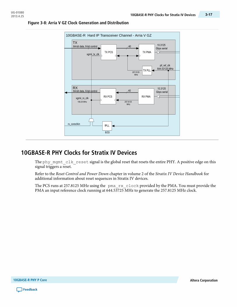
Figure 3-8: Arria V GZ Clock Generation and Distribution
pll_ref_clk644.53125 MHz
10.3125Gbps serial
257.8125MHz
257.8125MHz
156.25 MHz
10GBASE-R Hard IP Transceiver Channel - Arria V GZ
TX
RX
TX PCS
40
TX PMA
10.3125Gbps serial
RX PCS
40
RX PMA
TX PLL
8/33
fPLL
xgmii_rx_clk
rx_coreclkin
xgmii_tx_clk
64-bit data, 8-bit control
64-bit data, 8-bit control
10GBASE-R PHY Clocks for Stratix IV DevicesThe phy_mgmt_clk_reset signal is the global reset that resets the entire PHY. A positive edge on thissignal triggers a reset.
Refer to the Reset Control and Power Down chapter in volume 2 of the Stratix IV Device Handbook foradditional information about reset sequences in Stratix IV devices.
The PCS runs at 257.8125 MHz using the pma_rx_clock provided by the PMA. You must provide thePMA an input reference clock running at 644.53725 MHz to generate the 257.8125 MHz clock.
Altera Corporation10GBASE-R PHY P Core
Feedback
3-1710GBASE-R PHY Clocks for Stratix IV DevicesUG-010802013.4.25

Figure 3-9: Stratix IV Clock Generation and Distribution
pll_ref_clk644.53125 MHz
10.3125Gbps serial
516.625MHz
257.8125MHz
516.625MHz
257.8125MHz
156.25 MHz
10GBASE-R Transceiver Channel - Stratix IV GT
TX
RX
TX PCS(hard IP)
TX PCS(soft IP)
204064-bit data, 8-bit control
64-bit data, 8-bit control
TX PMA
/2
10.3125Gbps serial
RX PCS(hard IP)
RX PCS(soft IP)
2040
RX PMA
/2
5/4
TX PLL
8/33
GPLL
xgmii_rx_clk
xgmii_tx_clk
Related InformationReset Control and Power Down
10GBASE-R PHY Clocks for Stratix V DevicesThe following figure illustrates clock generation and distribution in Stratix V devices.
10GBASE-R PHY P CoreAltera Corporation
Feedback
UG-0108010GBASE-R PHY Clocks for Stratix V Devices3-18 2013.4.25

Figure 3-10: Stratix V Clock Generation and Distribution
pll_ref_clk644.53125 MHz
10.3125Gbps serial
257.8125MHz
257.8125MHz
156.25 MHz
10GBASE-R Hard IP Transceiver Channel - Stratix V
TX
RX
TX PCS
40
TX PMA
10.3125Gbps serial
RX PCS
40
RX PMA
TX PLL
8/33
fPLL
xgmii_rx_clk
rx_coreclkin
xgmii_tx_clk
64-bit data, 8-bit control
64-bit data, 8-bit control
To ensure proper functioning of the PCS, the maximum PPM difference between the pll_ref_clk andxgmii_tx_clk clock inputs is 0 PPM. The FIFO in the RX PCS can compensate ±100 PPM between theRX PMA clock and xgmii_rx_clk. You should use xgmii_rx_clk to drive xgmii_tx_clk. TheCDR logic recovers 257.8125 MHz clock from the incoming data.
10GBASE-R PHY Register Interface and Register DescriptionsThe Avalon-MM PHY management interface provides access to the 10GBASER-R PHY PCS and PMAregisters. You can use an embedded controller acting as an Avalon-MM master to send read and writecommands to this Avalon-MM slave interface.
Table 3-14: Avalon-MM PHY Management Interface
DescriptionDirectionSignal Name
The clock signal that controls the Avalon-MM PHYmanagement, interface. For Stratix IV devices, thefrequency range is 37.5-50 MHz. There is nofrequency restriction for Stratix V devices; however,if you plan to use the same clock for the PHYmanagement interface and transceiverreconfiguration, youmust restrict the frequency rangeof phy_mgmt_clk to 100-150 MHz to meet thespecification for the transceiver reconfiguration clock.
Inputphy_mgmt_clk
Altera Corporation10GBASE-R PHY P Core
Feedback
3-1910GBASE-R PHY Register Interface and Register DescriptionsUG-010802013.4.25

DescriptionDirectionSignal Name
Global reset signal that resets the entire 10GBASE-RPHY. This signal is active high and level sensitive.
Inputphy_mgmt_clk_reset
9-bit Avalon-MM address.Inputphy_mgmt_addr[8:0]
Input data.Inputphy_mgmt_writedata[31:0]
Output data.Outputphy_mgmt_readdata[31:0]
Write signal. Asserted high.Inputphy_mgmt_write
Read signal. Asserted high.Inputphy_mgmt_read
When asserted, indicates that the Avalon-MM slaveinterface is unable to respond to a read or writerequest. When asserted, control signals to theAvalon-MM slave interface must remain constant.
Outputphy_mgmt_waitrequest
Refer to the “Typical Slave Read and Write Transfers” and “Master Transfers” sections in the “AvalonMemory-Mapped Interfaces” chapter of the Avalon Interface Specifications for timing diagrams.
The following table specifies the registers that you can access over the Avalon-MM PHY managementinterface using word addresses and a 32-bit embedded processor. A single address space provides access toall registers.
Writing to reserved or undefined register addresses may have undefined side effects.Note:
Table 3-15: 10GBASE-R Register Descriptions
DescriptionNameR/WBitWord Addr
PMA Common Control and Status
Writing a 1 to channel <n> powers downthe calibration block for channel <n>. Thisregister is only available if you select Useexternal PMAcontrol and reconfig on theAdditional Options tab of the GUI.
cal_blk_powerdownRW[31:0]0x021
Bit[P] indicates that the TX clockmultiplierunit CMU PLL [P] is locked to the inputreference clock. This register is onlyavailable if you select Use external PMAcontrol and reconfig on the AdditionalOptions tab of the GUI.
pma_tx_pll_is_lockedRO[31:0]0x022
Reset Control Registers-Automatic Reset Controller
Reset controller channel bitmask for digitalresets. The default value is all 1 s. Channel<n> can be reset when bit<n> = 1. Channel<n> cannot be reset when bit<n>=0.
reset_ch_bitmaskRW[31:0]0x041
10GBASE-R PHY P CoreAltera Corporation
Feedback
UG-0108010GBASE-R PHY Register Interface and Register Descriptions3-20 2013.4.25

DescriptionNameR/WBitWord Addr
Writing a 1 to bit 0 initiates a TX digitalreset using the reset controllermodule. Thereset affects channels enabled in thereset_ch_bitmask. Writing a 1 to bit1 initiates a RX digital reset of channelsenabled in the reset_ch_bitmask.Both bits 0 and 1 self-clear.
reset_control (write)WO
[1:0]0x042
Reading bit 0 returns the status of the resetcontroller TX ready bit. Reading bit 1returns the status of the reset controller RXready bit.
reset_status (read)RO
You canuse thereset_fine_controlregister to create your own reset sequence.The reset control module performs astandard reset sequence at power on andwhenever thephy_mgmt_clk_reset isasserted. Bits [31:4,0] are reserved.
reset_fine_controlRW[31:0]
0x044
It is safe to write 0s to reserved bits.ReservedRW[31:4,0]
Writing a 1 causes the internal TX digitalreset signal to be asserted, resetting allchannels enabled in reset_ch_bitmask. You must write a 0 to clear thereset condition.
reset_tx_digitalRW[1]
Writing a 1 causes the internal RX digitalreset signal to be asserted, resetting the RXanalog logic of all channels enabled inreset_ch_bitmask. You must write a0 to clear the reset condition.
reset_rx_analogRW[2]
Writing a 1 causes the RX digital resetsignal to be asserted, resetting the RXdigitalchannels enabled in reset_ch_bitmask. You must write a 0 to clear thereset condition.
reset_rx_digitalRW[3]
PMA Channel Control and Status
[31:0]0x061
Writing a 1 to channel <n> puts channel<n> in serial loopback mode. Forinformation about pre- or post-CDR serialloopbackmodes, refer to LoopbackModes.
phy_serial_loopbackRW
When set, programs the RX CDR PLL tolock to the incoming data. Bit <n>corresponds to channel <n>.
pma_rx_set_locktodata
RW[31:0]0x064
Altera Corporation10GBASE-R PHY P Core
Feedback
3-2110GBASE-R PHY Register Interface and Register DescriptionsUG-010802013.4.25

DescriptionNameR/WBitWord Addr
When set, programs the RX CDR PLL tolock to the reference clock. Bit <n>corresponds to channel <n>.
pma_rx_set_locktorefRW[31:0]0x065
When asserted, indicates that the RX CDRPLL is locked to the RX data, and that theRX CDR has changed from LTR to LTDmode. Bit <n> corresponds to channel <n>.
pma_rx_is_lockedtodata
RO[31:0]0x066
When asserted, indicates that the RX CDRPLL is locked to the reference clock. Bit <n>corresponds to channel <n>.
pma_rx_is_lockedtoref
RO[31:0]0x067
10GBASE-R PCS
INDIRECT_ADDRWO[31:0]0x080
Provides for indirect addressing of all PCScontrol and status registers. Use this registerto specify the logical channel number of thePCS channel you want to access.
When set to 1, clears the error block countregister. To block: Block synchronizer
RCLR_ERRBLK_CNTRW[2]
0x081When set to 1, clears the bit error rate(BER) register. To block: BER monitor
RCLR_BER_COUNTRW[3]
For Stratix IV devices: When assertedindicates that the PCS link is up.
PCS_STATUSR[0]
0x082
When asserted by the BER monitor block,indicates that the PCS is recording a highBER. From block: BER monitor
HI_BERR[1]
When asserted by the block synchronizer,indicates that the PCS is locked to receivedblocks. From Block: Block synchronizer
BLOCK_LOCKR[2]
When asserted, indicates the TX FIFO isfull. From block: TX FIFO
TX_FIFO_FULLR[3]
When asserted, indicates the RX FIFO isfull. From block: RX FIFO
RX_FIFO_FULLR[4]
For Stratix V devices, when asserted,indicates anRX synchronization error. Thissignal is Stratix V devices only.
RX_SYNC_HEAD_ERRORR[5]
For Stratix V devices: When asserted,indicates an RX scrambler error.
RX_SCRAMBLER_ERRORR[6]
When asserted indicates that the RXinterface is ready to send out received data.From block: 10 Gbps Receiver PCS
RX_DATA_READYR[7]
10GBASE-R PHY P CoreAltera Corporation
Feedback
UG-0108010GBASE-R PHY Register Interface and Register Descriptions3-22 2013.4.25

DescriptionNameR/WBitWord Addr
For Stratix IV devices only, records the biterror rate (BER).Fromblock: BERmonitor
BER_COUNT[5:0]R[5:0]
0x083 For Stratix IV devices only, records thenumber of blocks that contain errors.FromBlock: Block synchronizer
ERROR_BLOCK_COUNT[7:0]
R[13:6]
Related InformationAvalon Interface Specifications
Loopback Modes on page 16-50
10GBASE-R PHY Dynamic Reconfiguration for Stratix IV DevicesThe 10GBASE-R PHY includes additional top-level signals when configured with an external modules forPMA control and dynamic reconfiguration.
You enable this configuration by turning on Use external PMA control and reconfig available for StratixIV GT devices.
Table 3-16: External PMA and Reconfiguration Signals
DescriptionDirectionSignal Name
When asserted, powers down the entire GT block. Active high.For Stratix IV de
Inputgxb_pdn
When asserted, powers down the TX PLL. Active high.Inputpll_pdn
When asserted, powers down the calibration block. Active high.Inputcal_blk_pdn
Calibration clock. For Stratix IV devices only. It must be in therange 37.5-50 MHz. You can use the same clock for the phy_mgmt_clk and the cal_blk_clk.
Inputcal_blk_clk
When asserted, indicates that the TX PLL is locked.Outputpll_locked
Reconfiguration signals from the Transceiver ReconfigurationController to the PHYdevice. This signal is only available in StratixIV devices.
Inputreconfig_to_xcvr[3:0]
Reconfiguration RAM. The PHY device drives this RAM data tothe transceiver reconfiguration IP. This signal is only available inStratix IV devices.
Outputreconfig_from_xcvr[(<n>/4)17-1:0]
10GBASE-R PHY Dynamic Reconfiguration for Arria V and Stratix V DevicesFor Arria V and Stratix V devices, each channel and each TX PLL have separate dynamic reconfigurationinterfaces. The MegaWizard Plug-In Manager provides informational messages on the connectivity of theseinterfaces. The example below shows the messages for a single duplex channel.
Altera Corporation10GBASE-R PHY P Core
Feedback
3-2310GBASE-R PHY Dynamic Reconfiguration for Stratix IV DevicesUG-010802013.4.25

Although you must initially create a separate reconfiguration interface for each channel and TX PLL in yourdesign, when theQuartus II software compiles your design, it reduces the number of reconfiguration interfacesby merging reconfiguration interfaces. The synthesized design typically includes a reconfiguration interfacefor at least three channels because three channels share an Avalon-MM slave interface which connects tothe Transceiver Reconfiguration Controller IP Core. Conversely, you cannot connect the three channelsthat share an Avalon-MM interface to different Transceiver Reconfiguration Controllers. Doing so causesa Fitter error. For more information, refer to Transceiver Reconfiguration Controller to PHY IPConnectivity on page 16-48. Allowing the Quartus II software to merge reconfiguration interfaces givesthe Fitter more flexibility in placing transceiver channels.
Example 3-2: Informational Messages for the Transceiver Reconfiguration Interface
Reconfiguration interface offset 0 is connected to the transceiverchannel.
PHY IP will require 2 reconfiguration interfaces for connection tothe external reconfiguration controller.
Reconfiguration interface offset 0 is connected to the transceiverchannel.
Reconfiguration interface offset 1 is connected to the transmitPLL.
The following table describes the signals in the reconfiguration interface; this interface uses the Avalon-MMPHY Management interface clock.
Table 3-17: Reconfiguration Interface
DescriptionDirectionSignal Name
Reconfiguration signals from the Transceiver ReconfigurationController. <n> grows linearly with the number ofreconfiguration interfaces. This signal is only available in StratixV devices.
Inputreconfig_to_xcvr
[(<n>70-1):0]
Reconfiguration signals to the Transceiver ReconfigurationController. <n> grows linearly with the number ofreconfiguration interfaces. This signal is only available in StratixV devices.
Outputreconfig_from_xcvr
[(<n>46-1):0]
10GBASE-R PHY TimeQuest Timing ConstraintsThe timing constraints for Stratix IV GT designs are in alt_10gbaser_phy.sdc. If your design does not meettiming with these constraints, use LogicLock™ for the alt_10gbaser_pcs block. You can also applyLogicLock to the alt_10gbaser_pcs and slightly expand the lock region to meet timing.
The following example provides the Synopsys Design Constraints file (.sdc) timing constraints for the10GBASE-R IP Core when implemented in a Stratix IV device. To pass timing analysis, you must decouplethe clocks in different time domains. Be sure to verify the each clock domain is correctly buffered in the toplevel of your design. You can find the .sdc file in your top-level working directory. This is the same directorythat includes your top-level .v or .vhd file.
10GBASE-R PHY P CoreAltera Corporation
Feedback
UG-0108010GBASE-R PHY TimeQuest Timing Constraints3-24 2013.4.25
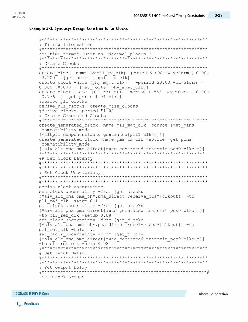
Example 3-3: Synopsys Design Constraints for Clocks
#**************************************************************# Timing Information#**************************************************************set_time_format -unit ns -decimal_places 3#**************************************************************# Create Clocks#**************************************************************create_clock -name {xgmii_tx_clk} -period 6.400 -waveform { 0.0003.200 } [get_ports {xgmii_tx_clk}]create_clock -name {phy_mgmt_clk} -period 20.00 -waveform {0.000 10.000 } [get_ports {phy_mgmt_clk}]create_clock -name {pll_ref_clk} -period 1.552 -waveform { 0.0000.776 } [get_ports {ref_clk}]#derive_pll_clocksderive_pll_clocks -create_base_clocks#derive_clocks -period "1.0"# Create Generated Clocks#**************************************************************create_generated_clock -name pll_mac_clk -source [get_pins-compatibility_mode{*altpll_component|auto_generated|pll1|clk[0]}]create_generated_clock -name pma_tx_clk -source [get_pins-compatibility_mode{*siv_alt_pma|pma_direct|auto_generated|transmit_pcs0|clkout}]**************************************************************## Set Clock Latency#**************************************************************#**************************************************************# Set Clock Uncertainty#**************************************************************#**************************************************************derive_clock_uncertaintyset_clock_uncertainty -from [get_clocks{*siv_alt_pma|pma_ch*.pma_direct|receive_pcs*|clkout}] -topll_ref_clk -setup 0.1set_clock_uncertainty -from [get_clocks{*siv_alt_pma|pma_direct|auto_generated|transmit_pcs0|clkout}]-to pll_ref_clk -setup 0.08set_clock_uncertainty -from [get_clocks{*siv_alt_pma|pma_ch*.pma_direct|receive_pcs*|clkout}] -topll_ref_clk -hold 0.1set_clock_uncertainty -from [get_clocks{*siv_alt_pma|pma_direct|auto_generated|transmit_pcs0|clkout}]-to pll_ref_clk -hold 0.08#**************************************************************# Set Input Delay#**************************************************************#**************************************************************# Set Output Delay#**************************************************************#Set Clock Groups
Altera Corporation10GBASE-R PHY P Core
Feedback
3-2510GBASE-R PHY TimeQuest Timing ConstraintsUG-010802013.4.25

#**************************************************************set_clock_groups -exclusive -group phy_mgmt_clk -groupxgmii_tx_clk -group [get_clocks{*siv_alt_pma|pma_ch*.pma_direct|transmit_pcs*|clkout}] -group[get_clocks {*siv_alt_pma|pma_ch*.pma_direct|receive_pcs*|clkout}]-group [get_clocks{*pll_siv_xgmii_clk|altpll_component|auto_generated|pll1|clk[0]}]
##**************************************************************# Set False Path#**************************************************************set_false_path -from{*siv_10gbaser_xcvr*clk_reset_ctrl|rx_pma_rstn} -to [get_clocks{{*siv_alt_pma|pma_ch*.pma_direct|transmit_pcs*|clkout}{*siv_alt_pma|pma_ch*.pma_direct|receive_pcs*|clkout}{*pll_siv_xgmii_clk|altpll_component|auto_generated|pll1|clk[0]}phy_mgmt_clk xgmii_tx_clk}]set_false_path -from{*siv_10gbaser_xcvr*clk_reset_ctrl|rx_usr_rstn} -to [get_clocks{{*siv_alt_pma|pma_ch*.pma_direct|transmit_pcs*|clkout}{*siv_alt_pma|pma_ch*.pma_direct|transmit_pcs*|clkout}{*pll_siv_xgmii_clk|altpll_component|auto_generated|pll1|clk[0]}phy_mgmt_clk xgmii_tx_clk}]set_false_path -from{*siv_10gbaser_xcvr*clk_reset_ctrl|tx_pma_rstn} -to [get_clocks{{*siv_alt_pma|pma_ch*.pma_direct|receive_pcs*|clkout}{*siv_alt_pma|pma_ch*.pma_direct|transmit_pcs*|clkout}{*pll_siv_xgmii_clk|altpll_component|auto_generated|pll1|clk[0]}phy_mgmt_clk xgmii_tx_clk}]set_false_path -from{*siv_10gbaser_xcvr*clk_reset_ctrl|tx_usr_rstn} -to [get_clocks{{*siv_alt_pma|pma_ch*.pma_direct|receive_pcs*|clkout}{*siv_alt_pma|pma_ch*.pma_direct|transmit_pcs*|clkout}{*pll_siv_xgmii_clk|altpll_component|auto_generated|pll1|clk[0]}phy_mgmt_clk xgmii_tx_clk}]set_false_path -from {*siv_10gbaser_xcvr*rx_analog_rst_lego|rinit}-to [get_clocks{{*siv_alt_pma|pma_ch*.pma_direct|receive_pcs*|clkout}{*siv_alt_pma|pma_ch*.pma_direct|transmit_pcs*|clkout}{*pll_siv_xgmii_clk|altpll_component|auto_generated|pll1|clk[0]}phy_mgmt_clk xgmii_tx_clk}]set_false_path -from{*siv_10gbaser_xcvr*rx_digital_rst_lego|rinit} -to [get_clocks{{*siv_alt_pma|pma_ch*.pma_direct|receive_pcs*|clkout}{*siv_alt_pma|pma_ch*.pma_direct|transmit_pcs*|clkout}{*pll_siv_xgmii_clk|altpll_component|auto_generated|pll1|clk[0]}phy_mgmt_clk xgmii_tx_clk}]#**************************************************************# Set Multicycle Paths#****************************************************************************************************************************# Set Maximum Delay#**************************************************************
10GBASE-R PHY P CoreAltera Corporation
Feedback
UG-0108010GBASE-R PHY TimeQuest Timing Constraints3-26 2013.4.25

#**************************************************************# Set Minimum Delay#**************************************************************#**************************************************************# Set Input Transition#**************************************************************
This .sdc file is only applicable to the 10GBASE-R PHY IP Core when compiled in isolation. Youcan use it as a reference to help in creating your own .sdc file.
Note:
For Arria V and Stratix V devices, timing constraints are built into the HDL code.Note:
Related InformationAbout LogicLock Regions
10GBASE-R PHY Simulation Files and Example TestbenchRefer to Running a Simulation Testbench for a description of the directories and files that the Quartus IIsoftware creates automatically when you generate your 10GBASE-R PHY IP Core.
Altera Corporation10GBASE-R PHY P Core
Feedback
3-2710GBASE-R PHY Simulation Files and Example TestbenchUG-010802013.4.25

4Backplane Ethernet 10GBASE-KR PHY IPCore
2013.4.25UG-01080 Subscribe Feedback
The Backplane Ethernet 10GBASE-KR PHY MegaCore® function is available for Stratix® V and Arria VGZ devices.
This transceiver PHY allows you to instantiate both the hard Standard PCS and the higher performancehard 10G PCS and hard PMA for a single Backplane Ethernet channel. It implements the functionalitydescribed in the IEEE Std 802.3ap-2007 Standard. Because each instance of the 10GBASE-KR PHY IP Coresupports a single channel, you can create multi-channel designs by instantiating more than one instance ofthe core. The following figure shows the 10GBASE-KR transceiver PHY and additional blocks that arerequired to implement this core in your design.
Figure 4-1: 10GBASE-KR PHY MegaCore Function and Supporting Blocks
Altera Device with 10.3125+ Gbps Serial Transceivers10GBASE-KR PHY MegaCore Function
Native PHY Hard IP
257.8MHz
40-b
40-b
TXSerialData
RXSerialData
CopperBackplane
322.265625 MHzor 644.53125 MHzReference Clock
62.5 MHz or 125 MHzReference Clock
LegendHard IP Soft IP
ATX/CMUTX PLLFor
10 GbE
ATX/CMUTX PLL
For 1 GbE
1.25 Gb/10.3125 GbHard PMA
LinkStatus
Sequencer
10 GbEthernetHard PCS
1 GbEthernetStandardHard PCS
To/From Modules in the PHY MegaCore
Control and StatusRegisters
Avalon-MMPHY Management
Interface
PCS ReconfigRequest
PMA ReconfigRequest
Optional1588 TX andRX LatencyAdjust 1Gand 10G
To/From1G/10GbEthernetMAC
RX GMII Data
TX GMII Data@ 125 MHz
RX XGMII Data
TX XGMII [email protected] MHz
1 GIGEPCS
10GBASE-KRAuto-Negotiation
10GBASE-KRLink Training
ISO9001:2008Registered
© 2013 Altera Corporation. All rights reserved. ALTERA, ARRIA, CYCLONE, HARDCOPY, MAX, MEGACORE, NIOS, QUARTUS and STRATIXwords and logos are trademarks of Altera Corporation and registered in the U.S. Patent and Trademark Office and in other countries. All other wordsand logos identified as trademarks or service marks are the property of their respective holders as described at www.altera.com/common/legal.html.Altera warrants performance of its semiconductor products to current specifications in accordance with Altera's standard warranty, but reserves theright to make changes to any products and services at any time without notice. Altera assumes no responsibility or liability arising out of the applicationor use of any information, product, or service described herein except as expressly agreed to in writing by Altera. Altera customers are advised toobtain the latest version of device specifications before relying on any published information and before placing orders for products or services.
www.altera.com
101 Innovation Drive, San Jose, CA 95134
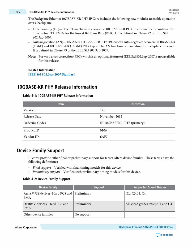
The Backplane Ethernet 10GBASE-KRPHY IPCore includes the following newmodules to enable operationover a backplane:
• Link Training (LT)— The LT mechanism allows the 10GBASE-KR PHY to automatically configure thelink-partner TX PMDs for the lowest Bit Error Rate (BER). LT is defined in Clause 72 of IEEE Std802.3ap-2007.
• Autonegotiation (AN)—TheAltera 10GBASE-KRPHYIPCore can auto-negotiate between1000BASE-KX(1GbE) and 10GBASE-KR (10GbE) PHY types. The AN function is mandatory for Backplane Ethernet.It is defined in Clause 73 of the IEEE Std 802.3ap-2007.
Forward error correction (FEC)which is an optional feature of IEEE Std 802.3ap-2007 is not availablefor this release.
Note:
Related InformationIEEE Std 802.3ap-2007 Standard
10GBASE-KR PHY Release Information
Table 4-1: 10GBASE-KR PHY Release Information
DescriptionItem
12.1Version
November 2012Release Date
IP-10GBASEKR PHY (primary)Ordering Codes
0106Product ID
6AF7Vendor ID
Device Family SupportIP cores provide either final or preliminary support for target Altera device families. These terms have thefollowing definitions:
• Final support—Verified with final timing models for this device.• Preliminary support—Verified with preliminary timing models for this device.
Table 4-2: Device Family Support
Supported Speed GradesSupportDevice Family
I3L, C3, I4, C4PreliminaryArria V GZ devices–Hard PCS andPMA
All speed grades except I4 and C4PreliminaryStratix V devices–Hard PCS andPMA
No supportOther device families
Backplane Ethernet 10GBASE-KR PHY IP CoreAltera Corporation
Feedback
UG-0108010GBASE-KR PHY Release Information4-2 2013.4.25

Altera verifies that the current version of the Quartus II software compiles the previous version of each IPcore. Any exceptions to this verification are reported in theMegaCore IPLibraryReleaseNotes andErrata.Altera does not verify compilation with IP core versions older than the previous release.
For speed grade information, refer to DC and Switching Characteristics for Stratix V Devices in theStratix V Device Datasheet.
Note:
Related InformationStratix V Device Datasheet
10GBASE-KR PHY Performance and Resource UtilizationThis topic provides performance and resource utilization for the IP core inArria VGZ and Stratix V devices.
The following table shows the typical expected resource utilization for selected configurations using thecurrent version of theQuartus II software targeting a StratixVGT (5SGTMC7K2F40C2) device. The numbersof ALMs and logic registers are rounded up to the nearest 100. Resource utilization numbers reflect changesto the resource utilization reporting starting in the Quartus II software v12.1 release 28 nm device familiesand upcoming device families.
Table 4-3: 10GBASE-KR PHY Performance and Resource Utilization
MemoryLogic RegistersALMsModule Options
07004001GbE 10GBASE-KR PHY only, no AN or LT
0170010001GbE 10GBASE-KR PHY with AN and Sequencer
0230021001GbE 10GBASE-KR PHY with LT and Sequencer,
0330027001GbE 10GBASE-KR PHY with AN, LT, andSequencer
1 (M20K)0010GBASE-KR MIF, Port A depth 256, width 16,ROM (For reconfiguration from low latency or1GbE mode)
1 (M20K)00Low Latency MIF, Port A depth 256, width 16,ROM (Required for auto-negotiation and linktraining.)
Parameterizing the 10GBASE-KR PHYThe10GBASE-KR PHY IP Core is available for the Arria VGZ and Stratix V device families. The IP variantallows you specify either the Backplane-KR or 1Gb/10Gb Ethernet variant. When you select theBackplane-KR variant, the Link Training (LT) and Auto Negotiation (AN) tabs appear. The 1Gb/10GbEthernet variant (1G/10GbE) does not implement LT and AN parameters.
Altera CorporationBackplane Ethernet 10GBASE-KR PHY IP Core
Feedback
4-310GBASE-KR PHY Performance and Resource UtilizationUG-010802013.4.25
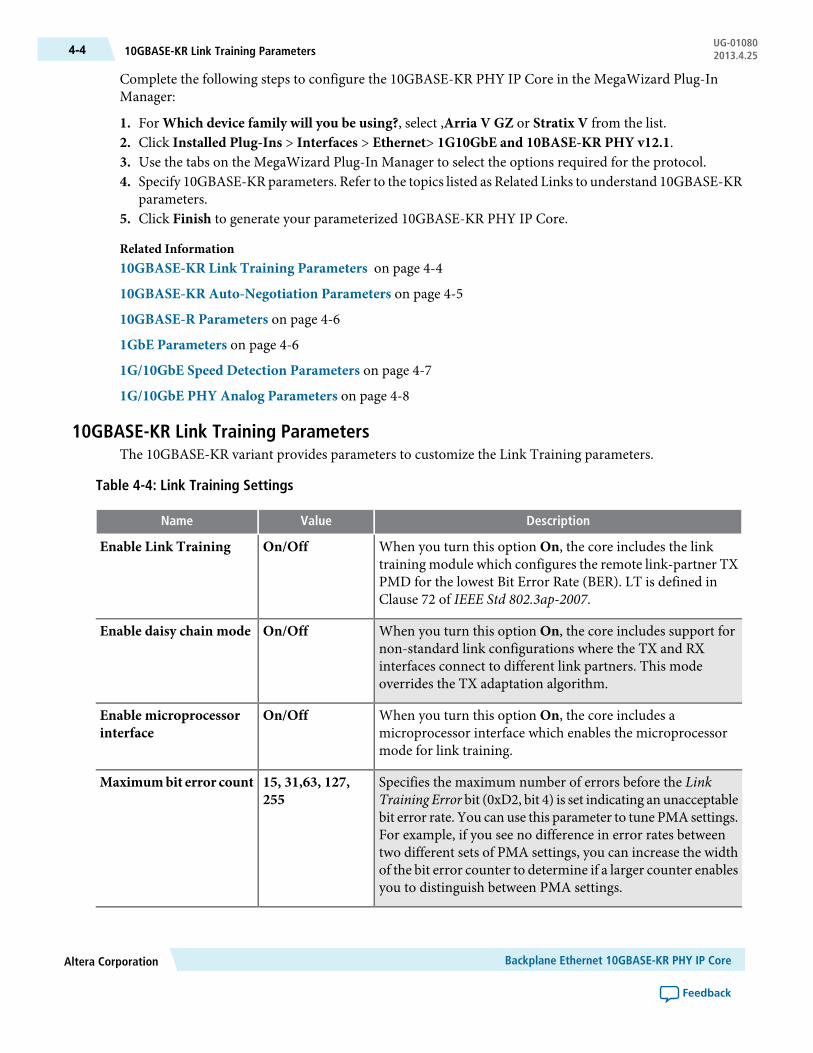
Complete the following steps to configure the 10GBASE-KR PHY IP Core in the MegaWizard Plug-InManager:
1. For Which device family will you be using?, select ,Arria V GZ or Stratix V from the list.2. Click Installed Plug-Ins > Interfaces > Ethernet> 1G10GbE and 10BASE-KR PHY v12.1.3. Use the tabs on the MegaWizard Plug-In Manager to select the options required for the protocol.4. Specify 10GBASE-KR parameters. Refer to the topics listed as Related Links to understand 10GBASE-KR
parameters.5. Click Finish to generate your parameterized 10GBASE-KR PHY IP Core.
Related Information10GBASE-KR Link Training Parameters on page 4-4
10GBASE-KR Auto-Negotiation Parameters on page 4-5
10GBASE-R Parameters on page 4-6
1GbE Parameters on page 4-6
1G/10GbE Speed Detection Parameters on page 4-7
1G/10GbE PHY Analog Parameters on page 4-8
10GBASE-KR Link Training ParametersThe 10GBASE-KR variant provides parameters to customize the Link Training parameters.
Table 4-4: Link Training Settings
DescriptionValueName
When you turn this option On, the core includes the linktraining module which configures the remote link-partner TXPMD for the lowest Bit Error Rate (BER). LT is defined inClause 72 of IEEE Std 802.3ap-2007.
On/OffEnable Link Training
When you turn this option On, the core includes support fornon-standard link configurations where the TX and RXinterfaces connect to different link partners. This modeoverrides the TX adaptation algorithm.
On/OffEnable daisy chain mode
When you turn this option On, the core includes amicroprocessor interface which enables the microprocessormode for link training.
On/OffEnable microprocessorinterface
Specifies the maximum number of errors before the LinkTraining Error bit (0xD2, bit 4) is set indicating an unacceptablebit error rate. You can use this parameter to tune PMA settings.For example, if you see no difference in error rates betweentwo different sets of PMA settings, you can increase the widthof the bit error counter to determine if a larger counter enablesyou to distinguish between PMA settings.
15, 31,63, 127,255
Maximumbit error count
Backplane Ethernet 10GBASE-KR PHY IP CoreAltera Corporation
Feedback
UG-0108010GBASE-KR Link Training Parameters4-4 2013.4.25
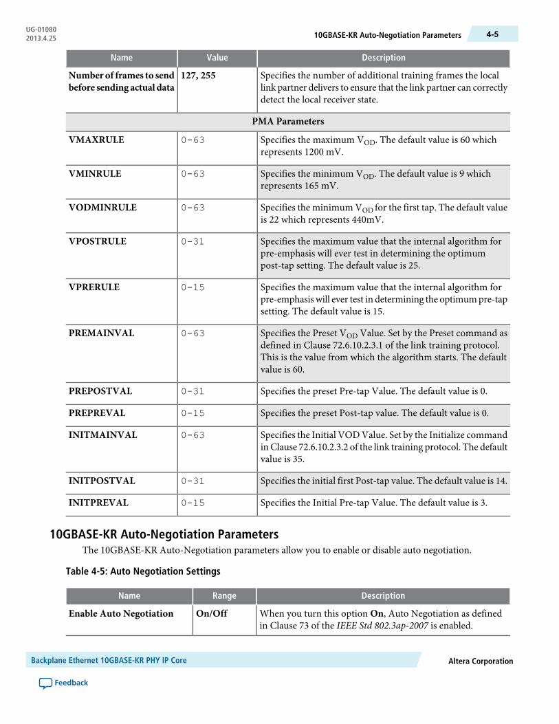
DescriptionValueName
Specifies the number of additional training frames the locallink partner delivers to ensure that the link partner can correctlydetect the local receiver state.
127, 255Numberof frames to sendbefore sending actual data
PMA Parameters
Specifies the maximum VOD. The default value is 60 whichrepresents 1200 mV.
0-63VMAXRULE
Specifies the minimum VOD. The default value is 9 whichrepresents 165 mV.
0-63VMINRULE
Specifies the minimum VOD for the first tap. The default valueis 22 which represents 440mV.
0-63VODMINRULE
Specifies the maximum value that the internal algorithm forpre-emphasis will ever test in determining the optimumpost-tap setting. The default value is 25.
0-31VPOSTRULE
Specifies the maximum value that the internal algorithm forpre-emphasis will ever test in determining the optimumpre-tapsetting. The default value is 15.
0-15VPRERULE
Specifies the Preset VOD Value. Set by the Preset command asdefined in Clause 72.6.10.2.3.1 of the link training protocol.This is the value from which the algorithm starts. The defaultvalue is 60.
0-63PREMAINVAL
Specifies the preset Pre-tap Value. The default value is 0.0-31PREPOSTVAL
Specifies the preset Post-tap value. The default value is 0.0-15PREPREVAL
Specifies the Initial VOD Value. Set by the Initialize commandinClause 72.6.10.2.3.2 of the link training protocol. The defaultvalue is 35.
0-63INITMAINVAL
Specifies the initial first Post-tap value. The default value is 14.0-31INITPOSTVAL
Specifies the Initial Pre-tap Value. The default value is 3.0-15INITPREVAL
10GBASE-KR Auto-Negotiation ParametersThe 10GBASE-KR Auto-Negotiation parameters allow you to enable or disable auto negotiation.
Table 4-5: Auto Negotiation Settings
DescriptionRangeName
When you turn this option On, Auto Negotiation as definedin Clause 73 of the IEEE Std 802.3ap-2007 is enabled.
On/OffEnable Auto Negotiation
Altera CorporationBackplane Ethernet 10GBASE-KR PHY IP Core
Feedback
4-510GBASE-KR Auto-Negotiation ParametersUG-010802013.4.25

DescriptionRangeName
When you turn this option On, the core supports symmetricpauses as defined in Annex 28B of Section 2 of IEEE Std802.3-2008.
On/OffPause Ability-C0
When you turn this option On, the core supports asymmetricpauses as defined in Annex 28B of Section 2 of IEEE Std802.3-2008.
On/OffPause Ability-C1
10GBASE-R ParametersThe 10GBASE-R parameters specify basic features of the 10GBASE-R PCS.
Table 4-6: 10GBASE-R Parameters
DescriptionOptionsParameter Name
When you turn this option On, the core includes logic toimplement the IEEE 1588 Precision Time Protocol.
On/OffEnable IEEE1588PrecisionTime Protocol
Specifies the input reference clock frequency. The defaultis 322.265625MHz.
644.53125MHz
322.265625MHz
Reference clock frequency
Specifies the PLL type. You can specify either a CMU orATX PLL. The ATX PLL has better jitter performance athigher data rates than the CMU PLL. Another advantageof theATXPLL is that it does not use a transceiver channel,while the CMU PLL does.
ATX
CMU
PLL Type
When you turn this optionOn, the core includes the rx_block_lock and rx_hi_ber ports.
On/OffEnable additional controland status pins
When you turn this option On, the core includes the rx_recovered_clk port.
On/OffEnable rx_recovered_clkpin
When you turn this optionOn, the core includes thepll_locked port.
On/OffEnable pll_locked statusport
Related InformationAnalog Settings for Arria V GZ Devices on page 19-9
Analog Settings for Stratix V Devices on page 19-25
1GbE ParametersThe 1GbE parameters allow you to specify options for the 1GbE mode.
Table 4-7: 1Gb Ethernet Parameters
DescriptionOptionsParameter Name
When you turn this optionOn, the core includes theGMIIinterface and related logic.
On/OffEnable 1Gb Ethernetprotocol
Backplane Ethernet 10GBASE-KR PHY IP CoreAltera Corporation
Feedback
UG-0108010GBASE-R Parameters4-6 2013.4.25
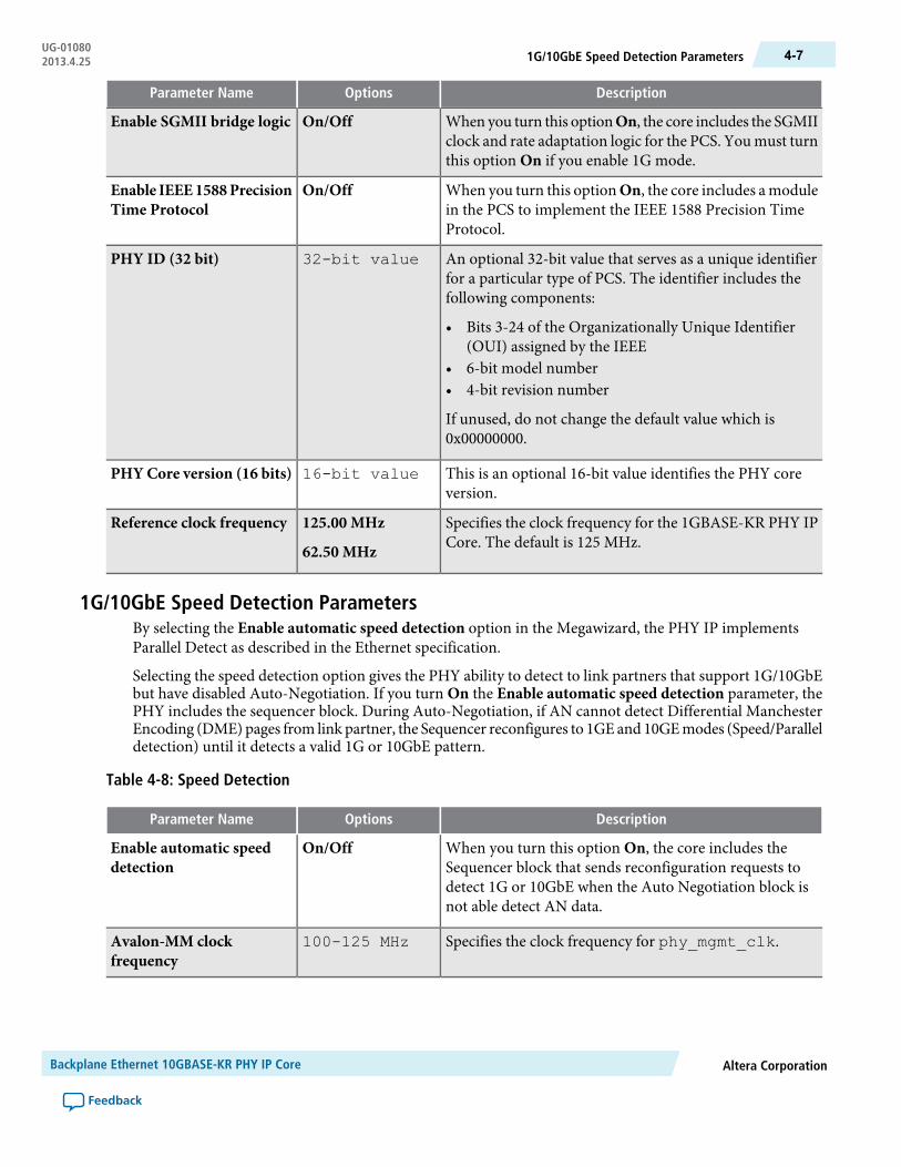
DescriptionOptionsParameter Name
When you turn this optionOn, the core includes the SGMIIclock and rate adaptation logic for the PCS. You must turnthis option On if you enable 1G mode.
On/OffEnable SGMII bridge logic
When you turn this optionOn, the core includes amodulein the PCS to implement the IEEE 1588 Precision TimeProtocol.
On/OffEnable IEEE1588PrecisionTime Protocol
An optional 32-bit value that serves as a unique identifierfor a particular type of PCS. The identifier includes thefollowing components:
• Bits 3-24 of the Organizationally Unique Identifier(OUI) assigned by the IEEE
• 6-bit model number• 4-bit revision number
If unused, do not change the default value which is0x00000000.
32-bit valuePHY ID (32 bit)
This is an optional 16-bit value identifies the PHY coreversion.
16-bit valuePHYCore version (16 bits)
Specifies the clock frequency for the 1GBASE-KR PHY IPCore. The default is 125 MHz.
125.00 MHz
62.50 MHz
Reference clock frequency
1G/10GbE Speed Detection ParametersBy selecting the Enable automatic speed detection option in the Megawizard, the PHY IP implementsParallel Detect as described in the Ethernet specification.
Selecting the speed detection option gives the PHY ability to detect to link partners that support 1G/10GbEbut have disabled Auto-Negotiation. If you turn On the Enable automatic speed detection parameter, thePHY includes the sequencer block. During Auto-Negotiation, if AN cannot detect Differential ManchesterEncoding (DME) pages from link partner, the Sequencer reconfigures to 1GE and 10GEmodes (Speed/Paralleldetection) until it detects a valid 1G or 10GbE pattern.
Table 4-8: Speed Detection
DescriptionOptionsParameter Name
When you turn this option On, the core includes theSequencer block that sends reconfiguration requests todetect 1G or 10GbE when the Auto Negotiation block isnot able detect AN data.
On/OffEnable automatic speeddetection
Specifies the clock frequency for phy_mgmt_clk.100-125 MHzAvalon-MM clockfrequency
Altera CorporationBackplane Ethernet 10GBASE-KR PHY IP Core
Feedback
4-71G/10GbE Speed Detection ParametersUG-010802013.4.25
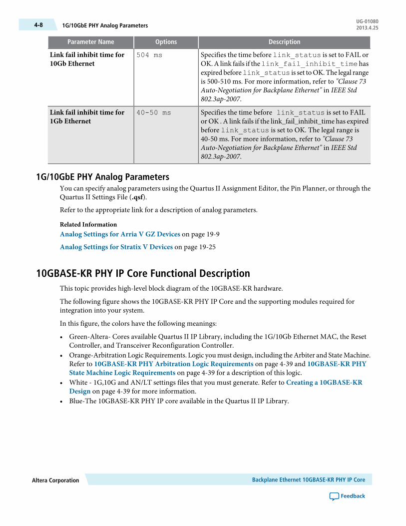
DescriptionOptionsParameter Name
Specifies the time before link_status is set to FAIL orOK.A link fails if thelink_fail_inhibit_timehasexpired beforelink_status is set toOK.The legal rangeis 500-510 ms. For more information, refer to "Clause 73Auto-Negotiation for Backplane Ethernet" in IEEE Std802.3ap-2007.
504 msLink fail inhibit time for10Gb Ethernet
Specifies the time before link_status is set to FAILor OK . A link fails if the link_fail_inhibit_time has expiredbefore link_status is set to OK. The legal range is40-50 ms. For more information, refer to "Clause 73Auto-Negotiation for Backplane Ethernet" in IEEE Std802.3ap-2007.
40-50 msLink fail inhibit time for1Gb Ethernet
1G/10GbE PHY Analog ParametersYou can specify analog parameters using the Quartus II Assignment Editor, the Pin Planner, or through theQuartus II Settings File (.qsf).
Refer to the appropriate link for a description of analog parameters.
Related InformationAnalog Settings for Arria V GZ Devices on page 19-9
Analog Settings for Stratix V Devices on page 19-25
10GBASE-KR PHY IP Core Functional DescriptionThis topic provides high-level block diagram of the 10GBASE-KR hardware.
The following figure shows the 10GBASE-KR PHY IP Core and the supporting modules required forintegration into your system.
In this figure, the colors have the following meanings:
• Green-Altera- Cores available Quartus II IP Library, including the 1G/10Gb Ethernet MAC, the ResetController, and Transceiver Reconfiguration Controller.
• Orange-Arbitration Logic Requirements. Logic youmust design, including theArbiter and StateMachine.Refer to 10GBASE-KR PHY Arbitration Logic Requirements on page 4-39 and 10GBASE-KR PHYState Machine Logic Requirements on page 4-39 for a description of this logic.
• White - 1G,10G and AN/LT settings files that you must generate. Refer to Creating a 10GBASE-KRDesign on page 4-39 for more information.
• Blue-The 10GBASE-KR PHY IP core available in the Quartus II IP Library.
Backplane Ethernet 10GBASE-KR PHY IP CoreAltera Corporation
Feedback
UG-010801G/10GbE PHY Analog Parameters4-8 2013.4.25
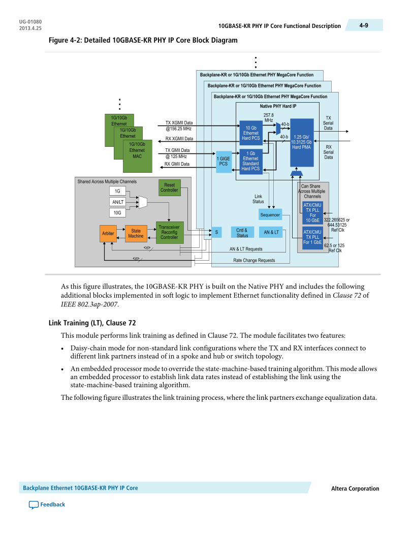
Figure 4-2: Detailed 10GBASE-KR PHY IP Core Block Diagram
58
1G/10GbEthernetMAC
Backplane-KR or 1G/10Gb Ethernet PHY MegaCore Function
Backplane-KR or 1G/10Gb Ethernet PHY MegaCore Function
Backplane-KR or 1G/10Gb Ethernet PHY MegaCore Function
Native PHY Hard IP
257.8MHz
40-b
40-bTX
SerialData
RXSerialData
322.265625 or644.53125Ref Clk
62.5 or 125Ref Clk
ATX/CMUTX PLLFor
10 GbE
ATX/CMUTX PLL
For 1 GbE
1.25 Gb/10.3125 GbHard PMA
LinkStatus
Sequencer
S
ResetController
StateMachineArbiter
Rate Change Requests
AN & LT Requests
TransceiverReconfigController
10 GbEthernetHard PCS
Cntl &Status
RX GMII Data
TX GMII Data@ 125 MHz
RX XGMII Data
TX XGMII Data
Shared Across Multiple ChannelsCan Share
Across MultipleChannels
@156.25 MHz
1 GIGEPCS
1G/10GbEthernetMAC1G/10Gb
EthernetMAC
1G
AN/LT
10G
1 GbEthernetStandardHard PCS
AN & LT
<n>
<n>
As this figure illustrates, the 10GBASE-KR PHY is built on the Native PHY and includes the followingadditional blocks implemented in soft logic to implement Ethernet functionality defined in Clause 72 ofIEEE 802.3ap-2007.
Link Training (LT), Clause 72
This module performs link training as defined in Clause 72. The module facilitates two features:
• Daisy-chain mode for non-standard link configurations where the TX and RX interfaces connect todifferent link partners instead of in a spoke and hub or switch topology.
• An embedded processormode to override the state-machine-based training algorithm. Thismode allowsan embedded processor to establish link data rates instead of establishing the link using thestate-machine-based training algorithm.
The following figure illustrates the link training process, where the link partners exchange equalization data.
Altera CorporationBackplane Ethernet 10GBASE-KR PHY IP Core
Feedback
4-910GBASE-KR PHY IP Core Functional DescriptionUG-010802013.4.25

Figure 4-3: TX Equalization for Link Partners
Rx
Encode
Handshake
Adapt
Tx
Eq
Decode Rx
Encode
Handshake
Adapt
Tx
Eq
Decode
CalculateBER
Send EqChange EqAck Change
Data Transmission Adaptation Feedback
1234
TX equalization includes the following steps which are identified in this figure.
1. The receiving link partner calculates the BER.2. The receiving link partner transmits an update to the transmitting link partner TX equalization parameters
to optimize the TX equalization settings3. The transmitting partner updates its TX equalization settings.4. The transmitting partner acknowledges the change.
This process is performed first for the VOD, then the pre-emphasis, the first post-tap, and then pre-emphasispre-tap.
The optional backplane daisy-chain topology can replace the spoke or hub switch topology. The followingillustration highlights the steps required for TX Equalization for Daisy Chain Mode.
Backplane Ethernet 10GBASE-KR PHY IP CoreAltera Corporation
Feedback
UG-0108010GBASE-KR PHY IP Core Functional Description4-10 2013.4.25
Figure 4-4: TX Equalization in Daisy-Chain Mode
RX
Encode
Handshake
Adapt
TX
dmi*
dmi*
dmi*
dmo*dmo*
Partner A
Parter C
Parter B
Eq
Decode
RX
Encode
Handshake
Adapt
TX
Eq
Decode
Change Eq
AckChange
Data Transmission
Adaptation Feedback
Change Eq
Ack Change
Feedback/Handshake via Management
RX
Encode
Handshake
Adapt
TX
Eq
Decode
Change Eq Ack Change
1
2
3
4
5
dmo*
Data transmission proceeds clockwise from link partner A, to B, to C. TX equalization includes the followingsteps which are identified in the figure :
1. The receiving partner B calculates the BER for data received from transmitting partner A.2. The receiving partner B sends updates for TX link partner C.3. The receiving link partner C transmits an update to the transmitting link partner A.4. Transmit partner A updates its equalization settings.5. Transmit partner A acknowledges the change.
This procedure is repeated for the other two link partners.
Sequencer
The Sequencer (Rate change) block controls the start-up (reset, power-on) sequence of the PHY IP. Itautomatically selects which PCS (1G, 10GbE, or Low Latency) is required and sends requests to reconfigurethe PCS. The Sequencer also performs the parallel detection function that reconfigures between the 1G and10GbE PCS until the link is established or times out.
Auto Negotiation (AN), Clause 73
The Auto Negotiation module in the 10GBASE-KR PHY IP implements Clause 73 of the Ethernet standard.Thismodule currently supports auto negotiation between 1GbE and 10GBASE-R data rates. Auto negotiationwith XAUI is not supported. Auto negotiation is run upon power up or if the auto negotiation module isreset.
The following figures illustrate the handshaking between the Auto Negotiation, Link Training, Sequencerand Transceiver Reconfiguration Controller blocks. The Transceiver Reconfiguration Controller uses
Altera CorporationBackplane Ethernet 10GBASE-KR PHY IP Core
Feedback
4-1110GBASE-KR PHY IP Core Functional DescriptionUG-010802013.4.25

lt_start_rc in conjunction with main_rc, post_rc, pre_rc, and tap_to_upd to change TXequalization settings.
Figure 4-5: Transition from Auto Negotiation to Link Training Mode
pcs_mode_rc[5:0]
lt_start_rc
rc_busy
seq_start_rc
tap_to_upd[2:0]
main_rc[5:0]
post_rc[4:0]
pre_rc[3:0]
111
60
0
0
59 5835
14
3
init state preset state
0201
TheTransceiverReconfigurationController usesseq_start_rc in combinationwith thepcs_mode_rcvalue to initiate a change to Auto Negotiation mode or from Link Training mode to 10GBASE-KR Datamode. After TX equalization completes, this timing diagram shows the transition from Link Training modeto 10GBASE-KR Data mode and MIF streaming.
Figure 4-6: Transition from Link Training to Data Mode
pcs_mode_rc[5:0]
lt_start_rc
seq_start_rc
MIF streamingrc_busy
tap_to_upd[2:0]
main_rc[5:0]
post_rc[4:0]
pre_rc[3:0]
04
5
9
42
001
02
Backplane Ethernet 10GBASE-KR PHY IP CoreAltera Corporation
Feedback
UG-0108010GBASE-KR PHY IP Core Functional Description4-12 2013.4.25
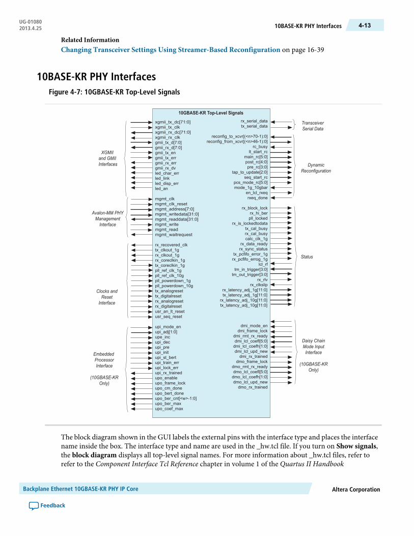
Related InformationChanging Transceiver Settings Using Streamer-Based Reconfiguration on page 16-39
10BASE-KR PHY InterfacesFigure 4-7: 10GBASE-KR Top-Level Signals
xgmii_tx_dc[71:0]xgmii_tx_clkxgmii_rx_dc[71:0]xgmii_rx_clkgmii_tx_d[7:0]gmii_rx_d[7:0]gmii_tx_engmii_tx_errgmii_rx_errgmii_rx_dvled_char_errled_linkled_disp_errled_an
mgmt_clkmgmt_clk_resetmgmt_address[7:0]mgmt_writedata[31:0]mgmt_readdata[31:0]mgmt_writemgmt_readmgmt_waitrequest
rx_recovered_clktx_clkout_1grx_clkout_1grx_coreclkin_1gtx_coreclkin_1gpll_ref_clk_1gpll_ref_clk_10gpll_powerdown_1gpll_powerdown_10gtx_analogresettx_digitalresetrx_analogresetrx_digitalresetusr_an_lt_resetusr_seq_reset
upi_mode_enupi_adj[1:0]upe_incupi_decupi_preupi_initupi_st_bertupi_train_errupi_lock_errupi_rx_trainedupo_enableupo_frame_lockupo_cm_doneupo_bert_doneupo_ber_cnt[<w>-1:0]upo_ber_maxupo_coef_max
10GBASE-KR Top-Level Signals
DynamicReconfiguration
rx_serial_datatx_serial_data
reconfig_to_xcvr[(<n>70-1):0]reconfig_from_xcvr[(<n>46-1):0]
rc_busylt_start_rc
main_rc[5:0]post_rc[4:0]pre_rc[3:0]
tap_to_update[2:0]seq_start_rc
pcs_mode_rc[5:0]mode_1g_10gbar
en_lcl_rxeqrxeq_done
rx_block_lockrx_hi_berpll_locked
rx_is_lockedtodatatx_cal_busyrx_cal_busycalc_clk_1g
rx_data_readyrx_sync_status
tx_pcfifo_error_1grx_pcfifo_errog_1g
lcl_rftm_in_trigger[3:0]
tm_out_trigger[3:0]rx_rlv
rx_clksliprx_latency_adj_1g[11:0]tx_latency_adj_1g[11:0]
rx_latency_adj_10g[11:0]tx_latency_adj_10g[11:0]
dmi_mode_endmi_frame_lock
dmi_rmt_rx_readydmi_lcl_coefl[5:0]dmi_lcl_coefh[1:0]dmi_lcl_upd_new
dmi_rx_traineddmo_frame_lock
dmo_rmt_rx_readydmo_lcl_coefl[5:0]dmo_lcl_coefh[1:0]dmo_lcl_upd_new
dmo_rx_trained
TransceiverSerial Data
XGMIIand GMIIInterfaces
Avalon-MM PHYManagementInterface
Daisy ChainMode InputInterface
(10GBASE-KROnly)
EmbeddedProcessorInterface
(10GBASE-KROnly)
Clocks andReset
Interface
Status
The block diagram shown in the GUI labels the external pins with the interface type and places the interfacename inside the box. The interface type and name are used in the _hw.tcl file. If you turn on Show signals,the block diagram displays all top-level signal names. For more information about _hw.tcl files, refer torefer to the Component Interface Tcl Reference chapter in volume 1 of the Quartus II Handbook
Altera CorporationBackplane Ethernet 10GBASE-KR PHY IP Core
Feedback
4-1310BASE-KR PHY InterfacesUG-010802013.4.25

Related InformationComponent Interface Tcl Reference
10GBASE-KR PHY Clock and Reset InterfacesThis topic provides a block diagram of the 10GBASE-KR clock and reset connectivity and describes theclock and reset signals.
Use the Transceiver PHY Reset Controller IP Core to automatically control the transceiver reset sequence.This reset controller also has manual overrides for the TX and RX analog and digital circuits to allow youto reset individual channels upon reconfiguration.
If you instantiate multiple channels within a transceiver bank they share TX PLLs. If a reset is applied to thisPLL, it will affect all channels. Altera recommends leaving the TX PLL free-running after the start-up resetsequence is completed. After a channel is reconfigured you can simply reset the digital portions of thatspecific channel instead of going through the entire reset sequence. For more information about reset, referto the "Transceiver PHYReset Controller IP Core" chapter in theAltera Transceiver PHY IPCore User Guide.
The following figure provides an overview of the clocking for this core.
Figure 4-8: Clocks for Standard and 10G PCS and TX PLLs
xgmii_rx_clk156.25 MHz
xgmii_tx_clk156.25 MHz
Native PHY
Stratix V STDRX PCS
Stratix VTX PMAtx_coreclkin_1g
125 MHz
Stratix VRX PMA
TX PLL
TX PLL
40
rx_pld_clk rx_pma_clk
TX serial data8GMII TX Data
72XGMII TX Data & Cntl
RX data
40 TX data
40
TX data
serial data
pll_ref_clk_10g644.53125 MHz
or322.265625 MHz
pll_ref_clk_1g125 MHz
or62.5 MHz
Stratix V STDTX PCS
tx_pld_clk tx_pma_clk
8GMII RX Data
pll_ref_clk_10g
72XGMII RX Data & Cntl recovered clk257.8125 MHz
rx_coreclkin_1g125 MHz
Stratix V 10GRX PCS
rx_pld_clk rx_pma_clk
Stratix V 10GTX PCS
tx_pld_clk tx_pma_clkfractional
PLL
(instantiateseparately)
GIGEPCS
GIGEPCS
The following table describes the clock and reset signals. The frequencies of the XGMII clocks increases to257.8125 MHz when you enable 1588.
Table 4-9: Clock and Reset Signals
DescriptionDirectionSignal Name
The RX clock which is recovered from the received data. Youcan use this clock as a reference to lock an external clock source.Its frequency is 125 or 156.25 MHz.
Outputrx_recovered_clk
Backplane Ethernet 10GBASE-KR PHY IP CoreAltera Corporation
Feedback
UG-0108010GBASE-KR PHY Clock and Reset Interfaces4-14 2013.4.25

DescriptionDirectionSignal Name
GMII TX clock for the 1G TX parallel data source interface.The frequency is 125 MHz.
Outputtx_clkout_1g
GMII RX clock for the 1G RX parallel data source interface.The frequency is 125 MHz.
Outputrx_clkout_1g
Clock to drive the read side of the RX phase compensationFIFO in the Standard PCS. The frequency is 125 MHz.
Inputrx_coreclkin_1g
Clock to drive the write side of the TX phase compensationFIFO in the Standard PCS. The frequency is 125 MHz.
Inputtx_coreclkin_1g
Reference clock for the PMA block for the 1G mode. Itsfrequency is 125 or 62.5 MHz.
Inputpll_ref_clk_1g
Reference clock for the PMA block in 10G mode. Its frequencyis 644.53125 or 322.265625 MHz.
Inputpll_ref_clk_10g
Resets the 1Gb TX PLLs.Inputpll_powerdown_1g
Resets the 10Gb TX PLLs.Inputpll_powerdown_10g
Resets the analog TX portion of the transceiver PHY.Inputtx_analogreset
Resets the digital TX portion of the transceiver PHY.Inputtx_digitalreset
Resets the analog RX portion of the transceiver PHY.Inputrx_analogreset
Resets the digital RX portion of the transceiver PHY.Inputrx_digitalreset
Resets only the AN and LT logic. This signal is only availablefor the 10GBASE-KR variants.
Inputusr_an_lt_reset
Resets the sequencer. Initiates a PCS reconfiguration, and mayrestart AN, LT or both if these modes are enabled.
Inputusr_seq_reset
Related InformationTransceiver PHY Reset Controller IP Core on page 17-1
Transceiver Reconfiguration Controller IP Core Overview on page 16-1
10GBASE-KR PHY Data InterfacesThe following table describes the signals in the XGMII and GMII interfaces. The MAC drives the TX XGMIIand GMII signals to the 10GBASE-KR PHY. The 10GBASE-KR PHY drives the RX XGMII or GMII signalsto the MAC.
Altera CorporationBackplane Ethernet 10GBASE-KR PHY IP Core
Feedback
4-1510GBASE-KR PHY Data InterfacesUG-010802013.4.25
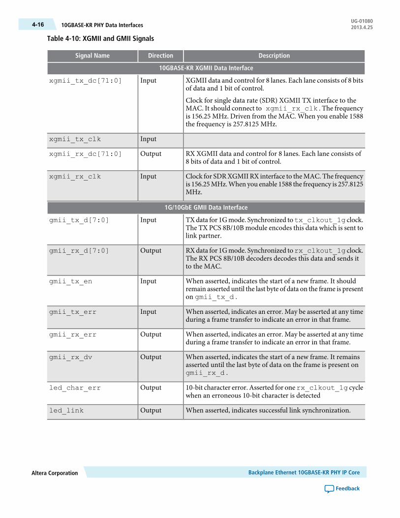
Table 4-10: XGMII and GMII Signals
DescriptionDirectionSignal Name
10GBASE-KR XGMII Data Interface
XGMII data and control for 8 lanes. Each lane consists of 8 bitsof data and 1 bit of control.
Clock for single data rate (SDR) XGMII TX interface to theMAC. It should connect to xgmii_rx_clk . The frequencyis 156.25 MHz. Driven from the MAC. When you enable 1588the frequency is 257.8125 MHz.
Inputxgmii_tx_dc[71:0]
Inputxgmii_tx_clk
RX XGMII data and control for 8 lanes. Each lane consists of8 bits of data and 1 bit of control.
Outputxgmii_rx_dc[71:0]
Clock for SDRXGMII RX interface to theMAC. The frequencyis 156.25MHz.When you enable 1588 the frequency is 257.8125MHz.
Inputxgmii_rx_clk
1G/10GbE GMII Data Interface
TXdata for 1Gmode. Synchronized totx_clkout_1g clock.The TX PCS 8B/10B module encodes this data which is sent tolink partner.
Inputgmii_tx_d[7:0]
RXdata for 1Gmode. Synchronized torx_clkout_1g clock.The RX PCS 8B/10B decoders decodes this data and sends itto the MAC.
Outputgmii_rx_d[7:0]
When asserted, indicates the start of a new frame. It shouldremain asserted until the last byte of data on the frame is presenton gmii_tx_d .
Inputgmii_tx_en
When asserted, indicates an error. May be asserted at any timeduring a frame transfer to indicate an error in that frame.
Inputgmii_tx_err
When asserted, indicates an error. May be asserted at any timeduring a frame transfer to indicate an error in that frame.
Outputgmii_rx_err
When asserted, indicates the start of a new frame. It remainsasserted until the last byte of data on the frame is present ongmii_rx_d .
Outputgmii_rx_dv
10-bit character error. Asserted for onerx_clkout_1g cyclewhen an erroneous 10-bit character is detected
Outputled_char_err
When asserted, indicates successful link synchronization.Outputled_link
Backplane Ethernet 10GBASE-KR PHY IP CoreAltera Corporation
Feedback
UG-0108010GBASE-KR PHY Data Interfaces4-16 2013.4.25
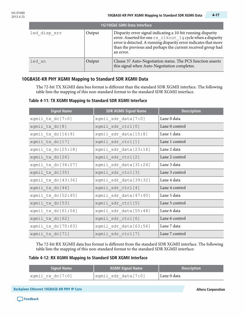
1G/10GbE GMII Data Interface
Disparity error signal indicating a 10-bit running disparityerror. Asserted for onerx_clkout_1g cyclewhen a disparityerror is detected. A running disparity error indicates that morethan the previous and perhaps the current received group hadan error.
Outputled_disp_err
Clause 37 Auto-Negotiation status. The PCS function assertsthis signal when Auto-Negotiation completes.
Outputled_an
10GBASE-KR PHY XGMII Mapping to Standard SDR XGMII Data
The 72-bit TX XGMII data bus format is different than the standard SDR XGMII interface. The followingtable lists the mapping of this non-standard format to the standard SDR XGMII interface.
Table 4-11: TX XGMII Mapping to Standard SDR XGMII Interface
DescriptionSDR XGMII Signal NameSignal Name
Lane 0 dataxgmii_sdr_data[7:0]xgmii_tx_dc[7:0]
Lane 0 controlxgmii_sdr_ctrl[0]xgmii_tx_dc[8]
Lane 1 dataxgmii_sdr_data[15:8]xgmii_tx_dc[16:9]
Lane 1 controlxgmii_sdr_ctrl[1]xgmii_tx_dc[17]
Lane 2 dataxgmii_sdr_data[23:16]xgmii_tx_dc[25:18]
Lane 2 controlxgmii_sdr_ctrl[2]xgmii_tx_dc[26]
Lane 3 dataxgmii_sdr_data[31:24]xgmii_tx_dc[34:27]
Lane 3 controlxgmii_sdr_ctrl[3]xgmii_tx_dc[35]
Lane 4 dataxgmii_sdr_data[39:32]xgmii_tx_dc[43:36]
Lane 4 controlxgmii_sdr_ctrl[4]xgmii_tx_dc[44]
Lane 5 dataxgmii_sdr_data[47:40]xgmii_tx_dc[52:45]
Lane 5 controlxgmii_sdr_ctrl[5]xgmii_tx_dc[53]
Lane 6 dataxgmii_sdr_data[55:48]xgmii_tx_dc[61:54]
Lane 6 controlxgmii_sdr_ctrl[6]xgmii_tx_dc[62]
Lane 7 dataxgmii_sdr_data[63:56]xgmii_tx_dc[70:63]
Lane 7 controlxgmii_sdr_ctrl[7]xgmii_tx_dc[71]
The 72-bit RX XGMII data bus format is different from the standard SDR XGMII interface. The followingtable lists the mapping of this non-standard format to the standard SDR XGMII interface:
Table 4-12: RX XGMII Mapping to Standard SDR XGMII Interface
DescriptionXGMII Signal NameSignal Name
Lane 0 dataxgmii_sdr_data[7:0]xgmii_rx_dc[7:0]
Altera CorporationBackplane Ethernet 10GBASE-KR PHY IP Core
Feedback
4-1710GBASE-KR PHY XGMII Mapping to Standard SDR XGMII DataUG-010802013.4.25
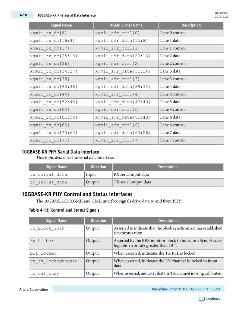
DescriptionXGMII Signal NameSignal Name
Lane 0 controlxgmii_sdr_ctrl[0]xgmii_rx_dc[8]
Lane 1 dataxgmii_sdr_data[15:8]xgmii_rx_dc[16:9]
Lane 1 controlxgmii_sdr_ctrl[1]xgmii_rx_dc[17]
Lane 2 dataxgmii_sdr_data[23:16]xgmii_rx_dc[25:18]
Lane 2 controlxgmii_sdr_ctrl[2]xgmii_rx_dc[26]
Lane 3 dataxgmii_sdr_data[31:24]xgmii_rx_dc[34:27]
Lane 3 controlxgmii_sdr_ctrl[3]xgmii_rx_dc[35]
Lane 4 dataxgmii_sdr_data[39:32]xgmii_rx_dc[43:36]
Lane 4 controlxgmii_sdr_ctrl[4]xgmii_rx_dc[44]
Lane 5 dataxgmii_sdr_data[47:40]xgmii_rx_dc[52:45]
Lane 5 controlxgmii_sdr_ctrl[5]xgmii_rx_dc[53]
Lane 6 dataxgmii_sdr_data[55:48]xgmii_rx_dc[61:54]
Lane 6 controlxgmii_sdr_ctrl[6]xgmii_rx_dc[62]
Lane 7 dataxgmii_sdr_data[63:56]xgmii_rx_dc[70:63]
Lane 7 controlxgmii_sdr_ctrl[7]xgmii_rx_dc[71]
10GBASE-KR PHY Serial Data InterfaceThis topic describes the serial data interface.
DescriptionDirectionSignal Name
RX serial input dataInputrx_serial_data
TX serial output dataOutputtx_serial_data
10GBASE-KR PHY Control and Status InterfacesThe 10GBASE-KR XGMII and GMII interface signals drive data to and from PHY.
Table 4-13: Control and Status Signals
DescriptionDirectionSignal Name
Asserted to indicate that the block synchronizer has establishedsynchronization.
Outputrx_block_lock
Asserted by the BER monitor block to indicate a Sync Headerhigh bit error rate greater than 10-4.
Outputrx_hi_ber
When asserted, indicates the TX PLL is locked.Outputpll_locked
When asserted, indicates the RX channel is locked to inputdata.
Outputrx_is_lockedtodata
When asserted, indicates that theTX channel is being calibrated.Outputtx_cal_busy
Backplane Ethernet 10GBASE-KR PHY IP CoreAltera Corporation
Feedback
UG-0108010GBASE-KR PHY Serial Data Interface4-18 2013.4.25

DescriptionDirectionSignal Name
When asserted, indicates that theRX channel is being calibrated.Outputrx_cal_busy
This clock is used for calculating the latency of the soft 1G PCSblock. This clock is only required for when you enable 1588 in1G mode.
Inputcalc_clk_1g
When asserted, indicates the Standard PCS word aligner hasaligned to in incoming word alignment pattern.
Outputrx_sync_status
When asserted, indicates that the Standard PCS TX phasecompensation FIFO is full.
Outputtx_pcfifo_error_1g
When asserted, indicates that the Standard PCS RX phasecompensation FIFO is full.
Outputrx_pcfifo_error_1g
When asserted, indicates a Remote Fault (RF).The MAC tosends this fault signal to its link partner. Remote Fault (RF) isencoded in bit D13 of the base Link Codeword. Bit 3 of theAuto Negotiation Advanced Remote Faultregister (0xC2) records this error.
Inputlcl_rf
This bus is not functional. Tie to 1'b0.Inputtrn_in_trigger[3:0]
This bus is not functional. You can leave this bus unconnected.Outputtrn_out_trigger[3:0]
When asserted, indicates a run length violation.Outputrx_rlv
When asserted, indicates that the deserializer has either skippedone serial bit or paused the serial clock for one cycle to achieveword alignment. As a result, the period of the parallel clockcould be extended by 1 unit interval (UI) during the clock slipoperation. This signal is available if you select the optional
Inputrx_clkslip
When you enable 1588, this signal outputs the real time latencyin GMII clock cycles (125 MHz) for the RX PCS and PMAdatapath for 1G mode.
Outputrx_latency_adj_1g[11:0]
When you enable 1588, this signal outputs real time latency inGMII clock cycles (125 MHz) for the TX PCS and PMAdatapath for 1G mode.
Outputtx_latency_adj_1g[11:0]
When you enable 1588, this signal outputs the real time latencyin XGMII clock cycles (156.25 MHz) for the RX PCS and PMAdatapath for 10G mode.
Outputrx_latency_adj_10g[11:0]
When you enable 1588, this signal outputs real time latency inXGMII clock cycles (156.25 MHz) for the TX PCS and PMAdatapath for 10G mode.
Outputtx_latency_adj_10g[11:0]
When asserted, indicates that the MAC can begin sending datato the 1G/10GbE PHY IP Core.
Outputrx_data_ready
10GBASE-KR PHY Link TrainingThis topic describes normal process link training which performs TX equalization. It includes a figureillustrating the steps involved.
Altera CorporationBackplane Ethernet 10GBASE-KR PHY IP Core
Feedback
4-1910GBASE-KR PHY Link TrainingUG-010802013.4.25

Figure 4-9: TX Equalization for Link Partners
The following figure illustrates the link training process, where the link partners exchange equalization data.
Rx
Encode
Handshake
Adapt
Tx
Eq
Decode Rx
Encode
Handshake
Adapt
Tx
Eq
Decode
CalculateBER
Send EqChange EqAck Change
Data Transmission Adaptation Feedback
1234
In the normal case, TX equalization includes the following steps which are identified in this figure.
1. The receiving link partner calculates the BER.2. The receiving link partner transmits an update to the transmitting link partner TX equalization parameters
to optimize the TX equalization settings3. The transmitting partner updates its TX equalization settings.4. The transmitting partner acknowledges the change.
This process is performed first for the VOD, then the pre-emphasis, the first post-tap, and then pre-emphasispre-tap.
10GBASE-KR PHY Daisy-Chain ModeThe optional backplane daisy-chain topology can replace the spoke or hub switch topology. The illustrationhighlights the steps required for TX Equalization in Daisy Chain Mode.
Backplane Ethernet 10GBASE-KR PHY IP CoreAltera Corporation
Feedback
UG-0108010GBASE-KR PHY Daisy-Chain Mode4-20 2013.4.25

Figure 4-10: TX Equalization in Daisy-Chain Mode
RX
Encode
Handshake
Adapt
TX
dmi*
dmi*
dmi*
dmo*dmo*
Partner A
Parter C
Parter B
Eq
Decode
RX
Encode
Handshake
Adapt
TX
Eq
Decode
Change Eq
AckChange
Data Transmission
Adaptation Feedback
Change Eq
Ack Change
Feedback/Handshake via Management
RX
Encode
Handshake
Adapt
TX
Eq
Decode
Change Eq Ack Change
1
2
3
4
5
dmo*
Data transmission proceeds clockwise from link partner A, to B, to C. TX equalization includes the followingsteps which are identified in the figure :
1. The receiving partner B calculates the BER for data received from transmitting partner A.2. The receiving partner B sends updates for TX link partner C.3. The receiving link partner C transmits an update to the transmitting link partner A.4. Transmit partner A updates its equalization settings.5. Transmit partner A acknowledges the change.
This procedure is repeated for the other two link partners.
10GBASE-KR PHY Daisy-Chain Interface SignalsThe optional daisy-chain interface signals connect link partners using a daisy-chain topology.
Table 4-14: Daisy Chain Interface Signals
DescriptionDirectionSignal Name
When asserted, enable Daisy Chain mode.Inputdmi_mode_en
When asserted, the daisy chain state machine has locked to thetraining frames.
Inputdmi_frame_lock
Corresponds to bit 15 of Status report field.When asserted, theremote receiver.
Inputdmi_rmt_rx_ready
Altera CorporationBackplane Ethernet 10GBASE-KR PHY IP Core
Feedback
4-2110GBASE-KR PHY Daisy-Chain Interface SignalsUG-010802013.4.25

DescriptionDirectionSignal Name
Local update low bits[5:0]. In daisy-chained configurations,the local update coefficients substitute for the coefficients thatwould be set using Link Training.
Inputdmi_lcl_coefl[5:0]
Local update high bits[13:12]. In daisy-chained configurations,the local update coefficients substitute for the coefficients thatwould be set using Link Training.
Inputdmi_lcl_coefh[1:0]
When asserted, indicates a local update has occurred.Inputdmi_lcl_upd_new
When asserted, indicates that the state machine has finishedlocal training.
Inputdmi_rx_trained
When asserted, indicates that the state machine has locked tothe training frames.
Outputdmo_frame_lock
Corresponds to the link partner's remote receiver ready bit.Outputdmo_rmt_rx_ready
Local update low bits[5:0]. In daisy-chained configurations,the local update coefficients substitute for the coefficients thatwould be set using Link Training.
Outputdmo_lcl_coefl[5:0]
Local update high bits[13:12]. In daisy-chained configurations,the local update coefficients substitute for the coefficients thatwould be set using Link Training.
Outputdmo_lcl_coefh[1:0]
When asserted, indicates a local update has occurred.Outputdmo_lcl_upd_new
When asserted, indicates that the state machine has finishedlocal training.
Outputdmo_rx_trained
1G/10GbE PHY Embedded Processor Interface SignalsThe optional embedded processor interface signals allow you to use the embedded processor mode of LinkTraining. This mode overrides the TX adaptation algorithm and allows an embedded processor to initializethe link.
Table 4-15: Embedded Processor Interface Signals
DescriptionDirectionSignal Name
When asserted, enables embedded processor mode.Inputupi_mode_en
Selects the active tap. The following encodings are defined:
• 2'b01: Main tap• 2'b10: Post-tap• 2'b11: Pre-tap
Inputupi_adj[1:0]
When asserted, sends the increment command.Inputupi_inc
When asserted, sends the decrement command.Inputupi_dec
When asserted, sends the preset command.Inputupi_pre
Backplane Ethernet 10GBASE-KR PHY IP CoreAltera Corporation
Feedback
UG-010801G/10GbE PHY Embedded Processor Interface Signals4-22 2013.4.25

DescriptionDirectionSignal Name
When asserted, sends the initialize command.Inputupi_init
When asserted, starts the BER timer.Inputupi_st_bert
When asserted, indicates a training error.Inputupi_train_err
When asserted, the local RX interface is trained.Inputupi_rx_trained
When asserted, indicates that the 10GBASE-KR PHY IP Coreis ready to receive commands from the embedded processor.
Outputupo_enable
When asserted, indicates the receiver has achieved trainingframe lock.
Outputupo_frame_lock
When asserted, indicates the master state machine handshakeis complete.
Outputupo_cm_done
When asserted, indicates the BER timer is at its maximumcount.
Outputupo_bert_done
Records the BER count.Outputupo_ber_cnt[ <w>-1:0]
When asserted, the BER counter has rolled over.Outputupo_ber_max
When asserted, indicates that the remote coefficients are attheir maximum or minimum values.
Outputupo_coef_max
Register Interface SignalsThe Avalon-MM master interface signals provide access to all registers.
Refer to the Typical Slave Read and Write Transfers and Master Transfers sections in the AvalonMemory-Mapped Interfaces chapter of the Avalon Interface Specifications for timing diagrams.
Table 4-16: Avalon-MM Interface Signals
DescriptionDirectionSignal Name
The clock signal that controls the Avalon-MM PHYmanagement, interface. If you plan to use the same clock forthePHYmanagement interface and transceiver reconfiguration,you must restrict the frequency range to 100-125 MHz to meetthe specification for the transceiver reconfiguration clock.
Inputmgmt_clk
Resets the PHY management interface. This signal is activehigh and level sensitive.
Inputmgmt_clk_reset
8-bit Avalon-MM address.Inputmgmt_addr[7:0]
Input data.Inputmgmt_writedata[31:0]
Output data.Outputmgmt_readdata[31:0]
Write signal. Active high.Inputmgmt_write
Read signal. Active high.Inputmgmt_read
Altera CorporationBackplane Ethernet 10GBASE-KR PHY IP Core
Feedback
4-23Register Interface SignalsUG-010802013.4.25
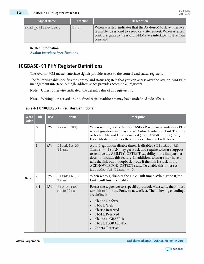
DescriptionDirectionSignal Name
When asserted, indicates that the Avalon-MM slave interfaceis unable to respond to a read or write request. When asserted,control signals to the Avalon-MM slave interface must remainconstant.
Outputmgmt_waitrequest
Related InformationAvalon Interface Specifications
10GBASE-KR PHY Register DefinitionsThe Avalon-MM master interface signals provide access to the control and status registers.
The following table specifies the control and status registers that you can access over the Avalon-MM PHYmanagement interface. A single address space provides access to all registers.
Unless otherwise indicated, the default value of all registers is 0.Note:
Writing to reserved or undefined register addresses may have undefined side effects.Note:
Table 4-17: 10GBASE-KR Register Definitions
DescriptionNameR/WBitWordAddr
When set to 1, resets the 10GBASE-KR sequencer, initiates a PCSreconfiguration, andmay restart Auto-Negotiation, Link Trainingor both if AN and LT are enabled (10GBASE-KR mode). SEQForce Mode[2:0] forces these modes. This reset self clears.
Reset SEQRW0
0xB0
Auto-Negotiation disable timer. If disabled ( Disable ANTimer = 1) , AN may get stuck and require software supportto remove the ABILITY_DETECT capability if the link partnerdoes not include this feature. In addition, software may have totake the link out of loopback mode if the link is stuck in theACKNOWLEDGE_DETECT state. To enable this timer setDisable AN Timer = 0.
Disable ANTimer
RW1
When set to 1, disables the Link Fault timer. When set to 0, theLink Fault timer is enabled.
Disable LFTimer
RW2
Forces the sequencer to a specific protocol. Must write theResetSEQ bit to 1 for the Force to take effect. The following encodingsare defined:
• 3'b000: No force• 3'b001: GigE• 3'b010: Reserved• 3'b011: Reserved• 3'b100: 10GBASE-R• 3'b101: 10GBASE-KR• Others: Reserved
SEQ ForceMode[2:0]
RW6:4
Backplane Ethernet 10GBASE-KR PHY IP CoreAltera Corporation
Feedback
UG-0108010GBASE-KR PHY Register Definitions4-24 2013.4.25
DescriptionNameR/WBitWordAddr
When asserted, the sequencer is indicating that the link is ready.SEQ Link ReadyR0
0xB1
When asserted, the sequencer has had an Auto-Negotiationtimeout. This bit is latched and is reset when the sequencer restartsAuto-Negotiation.
SEQ AN timeoutR1
When set, indicates that the Sequencer has had a timeout.SEQ LT timeout2
Specifies the Sequencer mode for PCS reconfiguration. Thefollowing modes are defined:
• Bit 8, mode[0]: AN mode• Bit 9, mode[1]: LT Mode• Bit 10, mode[2]: 10G data mode• Bit 11, mode[3]: Gige data mode• Bit 12, mode[4]: Reserved for XAUI• Bit13, mode[5]: Reserved
SEQ ReconfigMode[5:0]
13:8
When set to 1, enables Auto-Negotiation function. The defaultvalue is 1. For additional information, refer to bit 7.0.12 in Clause73.8 Management Register Requirements, of IEEE 802.3ap-2007.
AN enableRW0
0xC0
When set to 1, the user base pages are enabled. You can send anyarbitrary data via the user base page low/high bits. When set to 0,the user base pages are disabled and the state machine generatesthe base pages to send.
AN base pagesctrl
RW1
When set to 1, the user next pages are enabled. You can send anyarbitrary data via the user next page low/high bits. When set to 0,the user next pages are disabled. The state machine generates thenull message to send as next pages.
AN next pagesctrl
RW2
When set to 1, the local device signals Remote Faults in theAuto-Negotiation pages. When set to 0 a fault has not occurred.
Local deviceremote fault
R3
When set to 1, resets all the 10GBASE-KR Auto-Negotiation statemachines. This bit is self-clearing.
Reset ANRW0
0xC1
When set to 1, restarts the 10GBASE-KR TX state machine. Thisbit self clears. This bit is active only when the TX state machine isin the AN state. For more information, refer to bit 7.0.9 in Clause73.8 Management Register Requirements of IEEE 802.3ap-2007.
Restart AN TXSM
RW4
When asserted, new next page info is ready to send. The data is inthe XNP TX registers. When 0, the TX interface sends null pages.This bit self clears. Next Page (NP) is encoded in bit D15 of LinkCodeword. For more information, refer to Clause 73.6.9 and bit7.16.15 of Clause 45.2.7.6 of IEEE 802.3ap-2007.
AN Next PageRW8
Altera CorporationBackplane Ethernet 10GBASE-KR PHY IP Core
Feedback
4-2510GBASE-KR PHY Register DefinitionsUG-010802013.4.25

DescriptionNameR/WBitWordAddr
When set to 1, a page has been received. When 0, a page has notbeen received. The current value clears when the register is read.For more information, refer to bit 7.1.6 in Clause 73.8 of IEEE802.3ap-2007.
AN pagereceived
RO1
0xC2
When asserted, Auto-Negotiation has completed. When 0,Auto-Negotiation is in progress. For more information, refer tobit 7.1.5 in Clause 73.8 of IEEE 802.3ap-2007.
AN CompleteRO2
When set to 1, fault information has been sent to the link partner.When 0, a fault has not occurred. The current value clears whenthe register is read. Remote Fault (RF) is encoded in bit D13 of thebase LinkCodeword. Formore information, refer to Clause 73.6.7of and bit 7.16.13 of IEEE 802.3ap-2007.
AN ADV RemoteFault
RO3
When set to 1, the Auto-Negotiation state machine is in the idlestate. Incoming data is not Clause 73 compatible. When 0, theAuto-Negotiation is in progress.
AN RX SM IdleRO4
When set to 1, the transceiver PHY is able to performAuto-Negotiation. When set to 0, the transceiver PHY i s not ableto perform Auto-Negotiation. If your variant includesAuto-Negotiation, this bit is tied to 1. For more information, referto bits 7.1.3 and 7.48.0 of Clause 45 of IEEE 802.3ap-2007.
AN AbilityRO5
When set to 1, link is up. When 0, the link is down. The currentvalue clears when the register is read. For more information, referto bit 7.1.2 of Clause 45 of IEEE 802.3ap-2007.
AN StatusRO6
When set to 1, the link partner is able to performAuto-Negotiation.When 0, the link partner is not able to perform Auto-Negotiation.For more information, refer to bit 7.1.0 of Clause 45 of IEEE802.3ap-2007.
LP AN AbilityRO7
When set to 1, a sequencer Auto-Negotiation failure has beendetected. When set to 0, a Auto-Negotiation failure has not beendetected.
Seq AN FailureRO9
Provides a one-hot encoding of an_receive_idle = true and linkstatus for the supported link as described in Clause 73.10.1. Thefollowing encodings are defined:
• 6'b000000: 1000BASE-KX• 6'b000001 Reserved• 6'b000010: 10GBASE-KR• 6'b001000: Reserved• 6'b010000: Reserved• 6'b100000: Reserved
KR AN LinkReady[5:0]
RO17:12
Backplane Ethernet 10GBASE-KR PHY IP CoreAltera Corporation
Feedback
UG-0108010GBASE-KR PHY Register Definitions4-26 2013.4.25

DescriptionNameR/WBitWordAddr
The Auto-Negotiation TX state machine uses these bits if the ANbase pages ctrl bit is set. The following bits are defined:
• [15]: Next page bit• [14]: ACK which is controlled by the SM• [13]: Remote Fault bit• [12:10]: Pause bits• [9:5]: Echoed nonce which are set by the state machine• [4:0]: Selector
Bit 49, the PRBS bit, is generated by the Auto-Negotiation TX statemachine.
User base pagelow
RW15:00xC3
The Auto-Negotiation TX state machine uses these bits if theAuto-Negotiation base pages ctrl bit is set. The following bits aredefined:
• [29:5]: Correspond to page bit 45:21 which are the technologyability.
• [4:0]: Correspond to bits 20:16 which are TX nonce bits.
Bit 49, the PRBS bit, is generated by the Auto-Negotiation TX statemachine.
User base pagehigh
RW31:00xC4
The Auto-Negotiation TX state machine uses these bits if theAuto-Negotiation next pages ctrl bit is set. The following bits aredefined:
• [15]: next page bit• [14]: ACK controlled by the state machine• [13]: Message Page (MP) bit• [12]: ACK2 bit• [11]: Toggle bit
Formore information, refer toClause 73.7.7.1Next Page encodingsof IEEE 802.3ap-2007. Bit 49, the PRBS bit, is generated by theAuto-Negotiation TX state machine.
User Next pagelow
RW15:00xC5
The Auto-Negotiation TX state machine uses these bits if theAuto-Negotiation next pages ctrl bit is set. Bits [31:0] correspondto page bits [47:16]. Bit 49, the PRBS bit, is generated by theAuto-Negotiation TX state machine.
User Next pagehigh
RW31:00xC6
TheANRX statemachine received these bits from the link partner.The following bits are defined:
• [15] Next page bit• [14] ACK which is controlled by the state machine• [13] RF bit• [12:10] Pause bits• [9:5] Echoed Nonce which are set by the state machine• [4:0] Selector
LP base pagelow
RO15:00xC7
Altera CorporationBackplane Ethernet 10GBASE-KR PHY IP Core
Feedback
4-2710GBASE-KR PHY Register DefinitionsUG-010802013.4.25
DescriptionNameR/WBitWordAddr
TheANRX statemachine received these bits from the link partner.The following bits are defined:
• [31:30]: Reserved• [29:5]: Correspond to page bits [45:21]which are the technology
ability• [4:0]: Correspond to bits [20:16] which are TX Nonce bits
LP base pagehigh
RO31:00xC8
TheANRX statemachine receives these bits from the link partner.The following bits are defined:
• [15]: Next page bit• [14]: ACK which is controlled by the state machine• [13]: MP bit• [12] ACK2 bit• [11] Toggle bit
Formore information, refer toClause 73.7.7.1Next Page encodingsof IEEE 802.3ap-2007.
LP Next pagelow
RO15:00xC9
TheANRX statemachine receives these bits from the link partner.Bits [31:0] correspond to page bits [47:16]
LP Next pagehigh
RO31:00xCA
Received technology ability field bits of Clause 73Auto-Negotiation. The 10GBASE-KR PHY supports A0 and A2.The following protocols are defined:
• A0 1000BASE-KX• A1 10GBASE-KX4• A2 10GBASE-KR• A3 40GBASE-KR4• A4 40GBASE-CR4• A5 100GBASE-CR10• A24:6 are reserved
For more information, refer to Clause 73.6.4 and AN LP base pageability registers (7.19-7.21) of Clause 45 of IEEE 802.3ap-2007.
AN LP ADVTech_A[24:0]
RO24:0
0xCBReceived Remote Fault (RF) ability bits. RF is encoded in bit D13of the base link codeword inClause 73AN. Formore information,refer to Clause 73.6.7 and bits AN LP base page ability register ANLP base page ability registers (7.19-7.21) of Clause 45 of IEEE802.3ap-2007.
AN LP ADVRemote Fault
RO27
Received pause ability bits. Pause (C0:C1) is encoded in bitsD11:D10 of the base link codeword in Clause 73 AN as follows:
• C0 is the same as PAUSE as defined in Annex 28B• C1 is the same as ASM_DIR as defined in Annex 28B• C2 is reserved
For more information, refer to bits AN LP base page abilityregisters (7.19-7.21) of Clause 45 of IEEE 802.3ap-2007.
AN LP ADVPause Ability_C[2:0]
RO30:28
Backplane Ethernet 10GBASE-KR PHY IP CoreAltera Corporation
Feedback
UG-0108010GBASE-KR PHY Register Definitions4-28 2013.4.25

DescriptionNameR/WBitWordAddr
When 1, enables the 10GBASE-KR start-up protocol. When 0,disables the 10GBASE-KR start-up protocol. The default value is1. For more information, refer to Clause 72.6.10.3.1 and10GBASE-KR PMD control register bit (1.150.1) of IEEE802.3ap-2007.
Link Trainingenable
RW0
0xD0
When set to 1, disables the LT max_wait_timer . Used forcharacterizationmodewhen settingmuch longer BER timer values.
dis_max_wait_tmr
RW1
When set to 1, only the init and preset values are used to calculatethe best BER.
quick_modeRW2
When set to 1, the BER algorithm considers more than the firstlocal minimum when searching for the lowest BER. The defaultvalue is 1.
pass_oneRW3
Specifies the number of equalization steps for eachmain tap update.There are about 20 settings for the internal algorithm to test. Thevalid range is 1-15. The default value is 4'b0010.
main_step_cnt[3:0]
RW7:4
Specifies the number of equalization steps for each pre- and post-tap update. From 16-31 steps are possible. The default value is4'b0001.
prpo_step_cnt[3:0]
RW11:8
Adds hysteresis to the error count to avoid local minimums. Thedefault value is 2'b01.
equal_cnt[1:0]
RW13:12
When set to 1, overrides the link partner's equalization coefficients;software changes the update commands sent to the link partnerTX equalizer coefficients. When set to 0, uses the Link Traininglogic to determine the link partner coefficients. Used with 0xD1bit-4 and 0xD4 bits[7:0].
Ovride LP Coefenable
RW16
When set to 1, overrides the local device equalization coefficientsgeneration protocol. When set, the software changes the local TXequalizer coefficients. When set to 0, uses the update commandreceived from the link partner to determine local devicecoefficients. Used with 0xD1 bit-8 and 0xD4 bits[23:16]. Thedefault value is 1.
Ovride LocalRX Coef enable
RW17
Altera CorporationBackplane Ethernet 10GBASE-KR PHY IP Core
Feedback
4-2910GBASE-KR PHY Register DefinitionsUG-010802013.4.25

DescriptionNameR/WBitWordAddr
When set to 1, resets the 10GBASE-KR start-up protocol. Whenset to 0, continues normal operation. This bit self clears. For moreinformation, refer to the state variable mr_restart_training asdefined in Clause 72.6.10.3.1 and 10GBASE-KR PMD controlregister bit (1.150.0) IEEE 802.3ap-2007.
Restart Linktraining
RW0
0xD1
When sent to 1, there are new link partner coefficients availableto send. The LT logic starts sending the new values set in 0xD4bits[7:0] to the remote device. When set to 0, continues normaloperation. This bit self clears. Must enable this override in 0xD0bit16.
Updated TXCoef new
RW4
When set to 1, new local device coefficients are available. The LTlogic changes the local TX equalizer coefficients as specified in0xD4 bits[23:16]. When set to 0, continues normal operation. Thisbit self clears. Must enable the override in 0xD0 bit17.
Updated RXcoef new
RW8
When set to 1, the receiver is trained and is ready to receive data.When set to 0, receiver training is in progress. For moreinformation, refer to the state variable rx_trained as defined inClause 72.6.10.3.1 and bit 10GBASE-KR PMD control register bit10GBASE_KR PMD status register bit (1.151.0) of IEEE802.3ap-2007.
Link Trained -Receiverstatus
RO0
0xD2
When set to 1, the training frame delineation has been detected.When set to 0, the training frame delineation has not been detected.For more information, refer to the state variable frame_lock asdefined in Clause 72.6.10.3.1 and 10GBASE_KR PMD statusregister bit 10GBASE_KRPMDstatus register bit (1.151.1) of IEEE802.3ap-2007.
Link TrainingFrame lock
RO1
When set to 1, the start-up protocol is in progress. When set to 0,start-up protocol has completed. For more information, refer tothe state training as defined inClause 72.6.10.3.1 and 10GBASE_KRPMD status register bit (1.151.2) of IEEE 802.3ap-2007.
Link TrainingStart-upprotocolstatus
RO2
When set to 1, a training failure has been detected. When set to 0,a training failure has not been detected For more information,refer to the state variable training_failure as defined in Clause72.6.10.3.1 and bit 10GBASE_KRPMD status register bit (1.151.3)of IEEE 802.3ap-2007.
Link Trainingfailure
RO3
When set to 1, excessive errors occurred during Link Training.When set to 0, the BER is acceptable.
Link TrainingError
RO4
When set to 1, indicates a frame lockwas lost during LinkTraining.If the tap settings specified by the fields of 0xD5 are the same asthe initial parameter value, the frame lock error was unrecoverable.
Link TrainingFrame lockError
RO5
Backplane Ethernet 10GBASE-KR PHY IP CoreAltera Corporation
Feedback
UG-0108010GBASE-KR PHY Register Definitions4-30 2013.4.25
DescriptionNameR/WBitWordAddr
Specifies the number of training frames to examine for bit errorson the link for each step of the equalization settings. Used onlywhen ber_time_k_frames is 0.The following values are defined:
• A value of 2 is about 103 bytes• A value of 20 is about 104 bytes• A value of 200 is about 105 bytes
The default value for simulation is 2'b11. The default value forhardware is 0.
ber_time_frames
RW9:0
0xD3
Specifies the number of thousands of training frames to examinefor bit errors on the link for each step of the equalization settings.Set ber_time_m_frames = 0 for time/bits to match the followingvalues:
• A value of 3 is about 10 7 bits = about 1.3 ms• A value of 25 is about 10 8 bits = about 11ms• A value of 250 is about 10 9 bits = about 11 0ms
The default value for simulation is 0. The default value for hardwareis 0x15.
ber_time_k_frames
RW19:10
Specifies the number of millions of training frames to examine forbit errors on the link for each step of the equalization settings. Setber_time_k_frames = 4'd1000 = 0x3E8 for time/bits to match thefollowing values:
• A value of 3 is about 1010 bits = about 1.3 seconds• A value of 25 is about 10 11 bits = about 11 seconds• A value of 250 is about 1012 bits = about 110 seconds
ber_time_m_frames
RW29:20
Altera CorporationBackplane Ethernet 10GBASE-KR PHY IP Core
Feedback
4-3110GBASE-KR PHY Register DefinitionsUG-010802013.4.25

DescriptionNameR/WBitWordAddr
Reflects the contents of the first 16-bit word of the training framesent from the local device control channel. Normally, the bits inthis register are read-only; however, when you override trainingby setting the Ovride Coef enable control bit, these bits becomewriteable. The following fields are defined:
• [5: 4]: Coefficient (+1) update
• 2'b11: Reserved• 2'b01: Increment• 2'b10: Decrement• 2'b00: Hold
• [3:2]: Coefficient (0) update (same encoding as [5:4])• [1:0]: Coefficient (-1) update (same encoding as [5:4])
For more information, refer to bit 10G BASE-KR LD coefficientupdate register bits (1.154.5:0) in Clause 45.2.1.80.3 of IEEE802.3ap-2007.
LD coefficientupdate[5:0]
ROorRW
5:0
0xD4
When set to 1, requests the link partner coefficients be set toconfigure the TX equalizer to its INITIALIZE state. When set to0, continues normal operation. Formore information, refer to 10GBASE-KR LD coefficient update register bits (1.154.12) in Clause45.2.1.80.3 and Clause 72.6.10.2.3.2 of IEEE 802.3ap-2007.
LD InitializeCoefficients
ROorRW
6
When set to 1, requests the link partner coefficients be set to a statewhere equalization is turned off. When set to 0 the link operatesnormally. For more information, refer to bit 10G BASE-KR LDcoefficient update register bit (1.154.13) in Clause 45.2.1.80.3 andClause 72.6.10.2.3.2 of IEEE 802.3ap-2007.
LD PresetCoefficients
ROorRW
7
Status report register for the contents of the second, 16-bit wordof the training frame most recently sent from the local devicecontrol channel. The following fields are defined:
• [5:4]: Coefficient (post-tap)
• 2'b11: Maximum• 2'b01: Minimum• 2'b10: Updated• 2'b00: Not updated
• [3:2]: Coefficient (0) (same encoding as [5:4])• [1:0]: Coefficient (pre-tap) (same encoding as [5:4])
For more information, refer to bit 10G BASE-KR LD status reportregister bit (1.155.5:0) in Clause 45.2.1.81 of IEEE 802.3ap-2007.
LD coefficientstatus[5:0]
RO13:8
Link Trainingready - LDReceiver ready
RO14
Backplane Ethernet 10GBASE-KR PHY IP CoreAltera Corporation
Feedback
UG-0108010GBASE-KR PHY Register Definitions4-32 2013.4.25
DescriptionNameR/WBitWordAddr
When set to 1, the local device receiver has determined that trainingis complete and is prepared to receive data. When set to 0, the localdevice receiver is requesting that training continue. Values for thereceiver ready bit are defined in Clause 72.6.10.2.4.4. For moreinformation refer to For more information, refer to bit 10GBASE-KR LD status report register bit (1.155.15) in Clause45.2.1.81 of IEEE 802.3ap-2007.
Reflects the contents of the first 16-bit word of the training framemost recently received from the control channel.
Normally the bits in this register are read only; however, whentraining is disabled by setting low the KR Training enable controlbit, these bits become writeable. The following fields are defined:
• [5: 4]: Coefficient (+1) update
• 2'b11: Reserved• 2'b01: Increment• 2'b10: Decrement• 2'b00: Hold
• [3:2]: Coefficient (0) update (same encoding as [5:4])• [1:0]: Coefficient (-1) update (same encoding as [5:4])
For more information, refer to bit 10G BASE-KR LP coefficientupdate register bits (1.152.5:0) in Clause 45.2.1.78.3 of IEEE802.3ap-2007.
LP coefficientupdate[5:0]
ROorRW
21:16
When set to 1, the local device transmit equalizer coefficients areset to the INITIALIZE state. When set to 0, normal operationcontinues. The function and values of the initialize bit are definedin Clause 72.6.10.2.3.2. For more information, refer to bit 10GBASE-KR LP coefficient update register bits (1.152.12) in Clause45.2.1.78.3 of IEEE 802.3ap-2007.
LP InitializeCoefficients
ROorRW
22
When set to 1, The local device TX coefficients are set to a statewhere equalization is turned off. Preset coefficients are used.Whenset to 0, the local device operates normally. The function and valuesof the preset bit is defined in 72.6.10.2.3.1. The function and valuesof the initialize bit are defined in Clause 72.6.10.2.3.2. For moreinformation, refer to bit 10G BASE-KR LP coefficient updateregister bits (1.152.13) in Clause 45.2.1.78.3 of IEEE 802.3ap-2007.
LP PresetCoefficients
ROorRW
23
LP coefficientstatus[5:0]
RO29:24
Altera CorporationBackplane Ethernet 10GBASE-KR PHY IP Core
Feedback
4-3310GBASE-KR PHY Register DefinitionsUG-010802013.4.25

DescriptionNameR/WBitWordAddr
Status report register reflects the contents of the second, 16-bitword of the training framemost recently received from the controlchannel: The following fields are defined:
• [5:4]: Coefficient (+1)
• 2'b11: Maximum• 2'b01: Minimum• 2'b10: Updated• 2'b00: Not updated
• [3:2]: Coefficient (0) (same encoding as [5:4])• n [1:0]: Coefficient (-1) (same encoding as [5:4])
For more information, refer to bit 10G BASE-KR LP status reportregister bits (1.153.5:0) in Clause 45.2.1.79 of IEEE 802.3ap-2007.
When set to 1, the link partner receiver has determined thattraining is complete and is prepared to receive data. When set to0, the link partner receiver is requesting that training continue.
Values for the receiver ready bit are defined inClause 72.6.10.2.4.4.For more information, refer to bit 10G BASE-KR LP status reportregister bits (1.153.15) in Clause 45.2.1.79 of IEEE 802.3ap-2007.
LP Receiverready
RO30
Stores the most recent VOD setting that LT specified using theTransceiver Reconfiguration Controller IP core. It reflects LinkPartner commands to fine-tune the VOD.
LT VOD settingR5:0
0xD5Stores the most recent post-tap setting that LT specified using theTransceiver Reconfiguration Controller IP core. It reflects LinkPartner commands to fine-tune the TX pre-emphasis taps.
LT Post-tapsetting
R12:8
Stores the most recent pre-tap setting that LT specified using theTransceiver Reconfiguration Controller IP core. It reflects LinkPartner commands to fine-tune the TX pre-emphasis taps.
LT Pre-tapsetting
R19:16
Backplane Ethernet 10GBASE-KR PHY IP CoreAltera Corporation
Feedback
UG-0108010GBASE-KR PHY Register Definitions4-34 2013.4.25
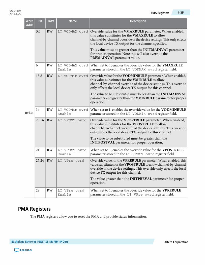
DescriptionNameR/WBitWordAddr
Override value for the VMAXRULE parameter. When enabled,this value substitutes for the VMAXRULE to allowchannel-by-channel override of the device settings. This only effectsthe local device TX output for the channel specified.
This value must be greater than the INITMAINVAL parameterfor proper operation. Note this will also override thePREMAINVAL parameter value.
LT VODMAX ovrdRW5:0
0xD6
When set to 1, enables the override value for the VMAXRULEparameter stored in the LT VODMAX ovrd register field.
LT VODMAX ovrdEnable
RW6
Override value for theVODMINRULE parameter.When enabled,this value substitutes for the VMINRULE to allowchannel-by-channel override of the device settings. This overrideonly effects the local device TX output for this channel.
The value to be substituted must be less than the INITMAINVALparameter and greater than theVMINRULE parameter for properoperation.
LT VODMin ovrdRW13:8
When set to 1, enables the override value for the VODMINRULEparameter stored in the LT VODMin ovrd register field.
LT VODMin ovrdEnable
RW14
Override value for the VPOSTRULE parameter. When enabled,this value substitutes for the VPOSTRULE to allowchannel-by-channel override of the device settings. This overrideonly effects the local device TX output for this channel.
The value to be substituted must be greater than theINITPOSTVAL parameter for proper operation.
LT VPOST ovrdRW20:16
When set to 1, enables the override value for the VPOSTRULEparameter stored in the LT VPOST ovrd register field.
LT VPOST ovrdEnable
RW21
Override value for theVPRERULE parameter.When enabled, thisvalue substitutes for theVPOSTRULE to allow channel-by-channeloverride of the device settings. This override only effects the localdevice TX output for this channel.
The value greater than the INITPREVAL parameter for properoperation.
LT VPre ovrdRW27:24
When set to 1, enables the override value for the VPRERULEparameter stored in the LT VPre ovrd register field.
LT VPre ovrdEnable
RW28
PMA RegistersThe PMA registers allow you to reset the PMA and provide status information.
Altera CorporationBackplane Ethernet 10GBASE-KR PHY IP Core
Feedback
4-35PMA RegistersUG-010802013.4.25
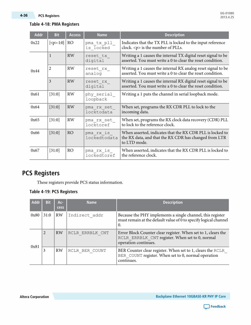
Table 4-18: PMA Registers
DescriptionNameAccessBitAddr
Indicates that the TX PLL is locked to the input referenceclock. <p> is the number of PLLs.
pma_tx_pll_is_locked
RO[<p>-1:0]0x22
Writing a 1 causes the internal TX digital reset signal to beasserted. You must write a 0 to clear the reset condition.
reset_tx_digital
RW1
0x44 Writing a 1 causes the internal RX analog reset signal to beasserted. You must write a 0 to clear the reset condition.
reset_rx_analog
RW2
Writing a 1 causes the internal RX digital reset signal to beasserted. You must write a 0 to clear the reset condition.
reset_rx_digital
RW3
Writing a 1 puts the channel in serial loopback mode.phy_serial_loopback
RW[31:0]0x61
When set, programs the RX CDR PLL to lock to theincoming data.
pma_rx_set_locktodata
RW[31:0]0x64
When set, programs the RX clock data recovery (CDR) PLLto lock to the reference clock.
pma_rx_set_locktoref
RW[31:0]0x65
When asserted, indicates that the RX CDR PLL is locked tothe RX data, and that the RX CDR has changed from LTRto LTD mode.
pma_rx_is_lockedtodata
RO[31:0]0x66
When asserted, indicates that the RX CDR PLL is locked tothe reference clock.
pma_rx_is_lockedtoref
RO[31:0]0x67
PCS RegistersThese registers provide PCS status information.
Table 4-19: PCS Registers
DescriptionNameAc-cess
BitAddr
Because the PHY implements a single channel, this registermust remain at the default value of 0 to specify logical channel0.
Indirect_addrRW31:00x80
Error Block Counter clear register. When set to 1, clears theRCLR_ERRBLK_CNT register. When set to 0, normaloperation continues.
RCLR_ERRBLK_CNTRW2
0x81BER Counter clear register. When set to 1, clears the RCLR_BER_COUNT register. When set to 0, normal operationcontinues.
RCLR_BER_COUNTRW3
Backplane Ethernet 10GBASE-KR PHY IP CoreAltera Corporation
Feedback
UG-01080PCS Registers4-36 2013.4.25
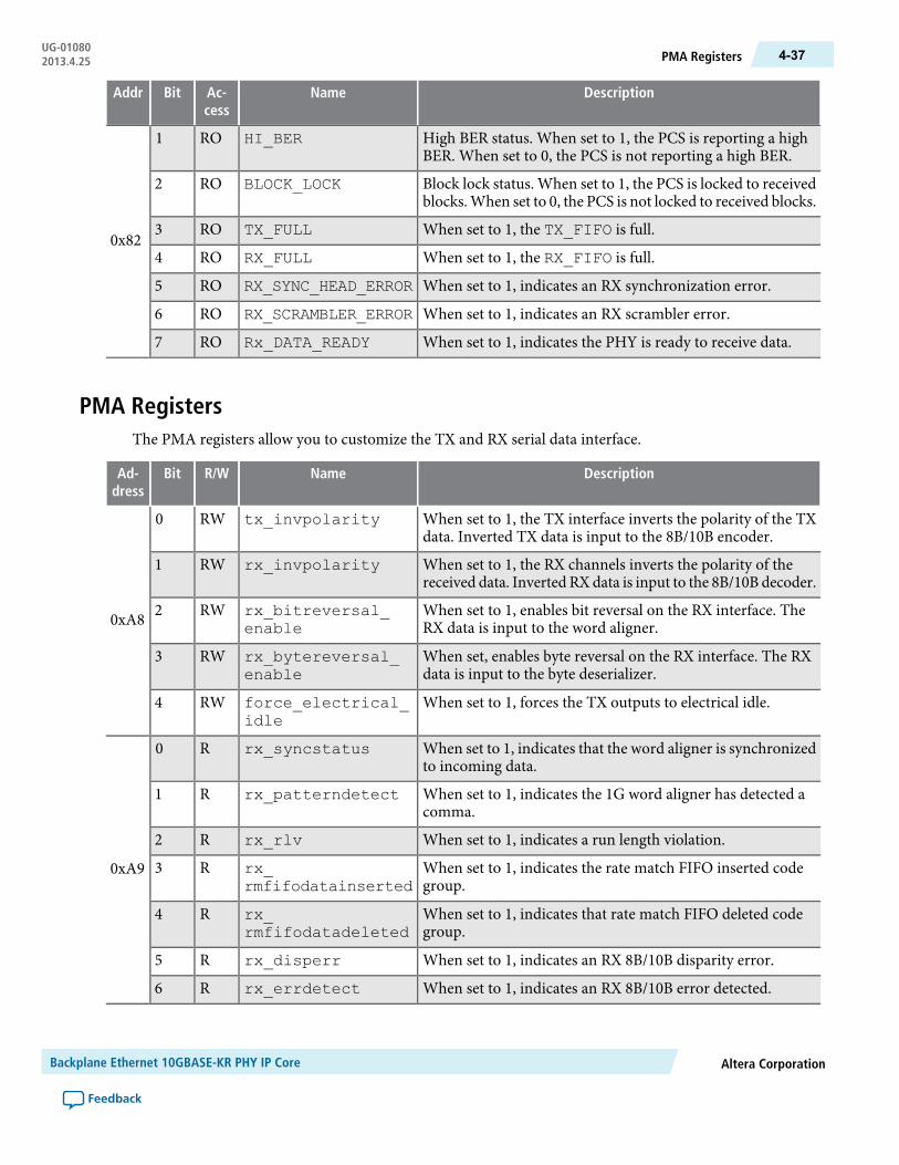
DescriptionNameAc-cess
BitAddr
High BER status. When set to 1, the PCS is reporting a highBER. When set to 0, the PCS is not reporting a high BER.
HI_BERRO1
0x82
Block lock status. When set to 1, the PCS is locked to receivedblocks. When set to 0, the PCS is not locked to received blocks.
BLOCK_LOCKRO2
When set to 1, the TX_FIFO is full.TX_FULLRO3
When set to 1, the RX_FIFO is full.RX_FULLRO4
When set to 1, indicates an RX synchronization error.RX_SYNC_HEAD_ERRORRO5
When set to 1, indicates an RX scrambler error.RX_SCRAMBLER_ERRORRO6
When set to 1, indicates the PHY is ready to receive data.Rx_DATA_READYRO7
PMA RegistersThe PMA registers allow you to customize the TX and RX serial data interface.
DescriptionNameR/WBitAd-dress
When set to 1, the TX interface inverts the polarity of the TXdata. Inverted TX data is input to the 8B/10B encoder.
tx_invpolarityRW0
0xA8
When set to 1, the RX channels inverts the polarity of thereceived data. Inverted RXdata is input to the 8B/10B decoder.
rx_invpolarityRW1
When set to 1, enables bit reversal on the RX interface. TheRX data is input to the word aligner.
rx_bitreversal_enable
RW2
When set, enables byte reversal on the RX interface. The RXdata is input to the byte deserializer.
rx_bytereversal_enable
RW3
When set to 1, forces the TX outputs to electrical idle.force_electrical_idle
RW4
When set to 1, indicates that the word aligner is synchronizedto incoming data.
rx_syncstatusR0
0xA9
When set to 1, indicates the 1G word aligner has detected acomma.
rx_patterndetectR1
When set to 1, indicates a run length violation.rx_rlvR2
When set to 1, indicates the rate match FIFO inserted codegroup.
rx_rmfifodatainserted
R3
When set to 1, indicates that rate match FIFO deleted codegroup.
rx_rmfifodatadeleted
R4
When set to 1, indicates an RX 8B/10B disparity error.rx_disperrR5
When set to 1, indicates an RX 8B/10B error detected.rx_errdetectR6
Altera CorporationBackplane Ethernet 10GBASE-KR PHY IP Core
Feedback
4-37PMA RegistersUG-010802013.4.25
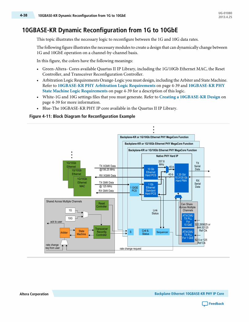
10GBASE-KR Dynamic Reconfiguration from 1G to 10GbEThis topic illustrates the necessary logic to reconfigure between the 1G and 10G data rates.
The following figure illustrates the necessarymodules to create a design that can dynamically change between1G and 10GbE operation on a channel-by-channel basis.
In this figure, the colors have the following meanings:
• Green-Altera- Cores available Quartus II IP Library, including the 1G/10Gb Ethernet MAC, the ResetController, and Transceiver Reconfiguration Controller.
• Arbitration Logic RequirementsOrange-Logic youmust design, including theArbiter and StateMachine.Refer to 10GBASE-KR PHY Arbitration Logic Requirements on page 4-39 and 10GBASE-KR PHYState Machine Logic Requirements on page 4-39 for a description of this logic.
• White-1G and 10G settings files that you must generate. Refer to Creating a 10GBASE-KR Design onpage 4-39 for more information.
• Blue-The 10GBASE-KR PHY IP core available in the Quartus II IP Library.
Figure 4-11: Block Diagram for Reconfiguration Example
1G/10GbEthernetMAC
Backplane-KR or 1G/10Gb Ethernet PHY MegaCore Function
Backplane-KR or 1G/10Gb Ethernet PHY MegaCore Function
Backplane-KR or 1G/10Gb Ethernet PHY MegaCore Function
Native PHY Hard IP
257.8MHz
40-b
40-bTX
SerialData
RXSerialData
322.265625 or644.53125Ref Clk
62.5 or 125Ref Clk
ATX/CMUTX PLLFor
10 GbE
ATX/CMUTX PLL
For 1 GbE
1.25 Gb/10.3125 GbHard PMA
LinkStatus
SequencerS
ResetController
StateMachineArbiter
rate change request
ack to user
rate changereq from user
TransceiverReconfigController
10 GbEthernetHard PCS
Cntl &Status
RX GMII Data
TX GMII Data@ 125 MHz
RX XGMII Data
TX XGMII Data
Shared Across Multiple ChannelsCan Share
Across MultipleChannels
@156.25 MHz
1 GIGEPCS
1G/10GbEthernetMAC1G/10Gb
EthernetMAC
1G
10G
1 GbEthernetStandardHard PCS
Backplane Ethernet 10GBASE-KR PHY IP CoreAltera Corporation
Feedback
UG-0108010GBASE-KR Dynamic Reconfiguration from 1G to 10GbE4-38 2013.4.25

Related InformationCreating a 10GBASE-KR Design on page 4-39
10GBASE-KR PHY Arbitration Logic RequirementsThis topic describes the arbitration functionality that you must implement.
The arbiter should implement the following logic. You can modify this logic based on your systemrequirements:
1. Accept requests from either the Sequencer or Link Training block. Prioritize requests to meet systemrequirements. Requests should consist of the following two buses:
• Channel number—specifies the requested channel• Mode—specifies 1G or 10G data modes or AN or LT modes for the corresponding channel
2. Select a channel for reconfiguration and send an ack/busy signal to the requestor. The requestor shoulddeassert its request signal when the ack/busy is received.
3. Pass the selected channel and rate information or PMA reconfiguration information for LT to the statemachine for processing.
4. Wait for a done signal from the state machine indicating that the reconfiguration process is completeand it is ready to service another request.
Related Information10GBASE-KR Dynamic Reconfiguration from 1G to 10GbE on page 4-38
10GBASE-KR PHY State Machine Logic RequirementsThe state machine should implement the following logic. You can modify this logic based on your systemrequirements:
1. Wait for reconfig_busy from the Transceiver Reconfiguration Controller to be deasserted and thetx_ready and rx_ready signals from the Transceiver PHY Reset Controller to be asserted. Theseconditions indicate that the system is ready to service a reconfiguration request.
2. Set the appropriate channel for reconfiguration.3. Initiate the MIF streaming process. The state machine should also select the appropriate MIF (stored in
the ROMs) to stream based on the requested mode.4. Wait for the reconfig_busy signal from the Transceiver Reconfiguration Controller to assert and
then deassert indicating the reconfiguration process is complete.5. Toggle the digital resets for the reconfigured channel and wait for the link to be ready.6. Deassert the ack/busy signal for the selected channel. Deassertion of ack/busy indicates to the
arbiter that the reconfiguration process is complete and the system is ready to service another request.
Related InformationTransceiver PHY Reset Controller IP Core on page 17-1
Transceiver Reconfiguration Controller IP Core Overview on page 16-1
Creating a 10GBASE-KR DesignHere are the steps you must take to create a 10GBASE-KR design using this PHY.
Altera CorporationBackplane Ethernet 10GBASE-KR PHY IP Core
Feedback
4-3910GBASE-KR PHY Arbitration Logic RequirementsUG-010802013.4.25

1. Generate the 10GBASE-KR PHY with the required parameterization.2. Generate a Transceiver Reconfiguration Controller with the correct number of reconfiguration interfaces
based on the number of channels you are using. This controller is connected to all the transceiver channels.It implements the reconfiguration process.
3. Generate a Transceiver Reset Controller.4. Create arbitration logic that prioritizes simultaneous reconfiguration requests from multiple channels.
This logic should also acknowledge the channel being serviced causing the requestor to deassert its requestsignal.
5. Create a state machine that controls the reconfiguration process. The state machine should:a. Receive the prioritized reconfiguration request from the arbiterb. Put the Transceiver Reconfiguration Controller into MIF streaming mode.c. Select the correct MIF and stream it into the appropriate channel.d. Wait for the reconfiguration process to end and provide status signal to arbiter.
6. Generate one ROM for each required configuration.7. Create a MIF for each configuration and associate each MIF with a ROM created in Step 6. For example,
create a MIF for 1G with 1588 , a MIF for 10G with 1588, and a MIF for AN/LT. AN/LT MIF is is usedto reconfigure the PHY into low latency mode during AN/LT. These MIFs are the three configurationsused in the MIF streaming process. The example design contains five required MIFs (1G, 10G, 1G with1588,10G with 1588 and AN/LT). Altera recommends that you use these MIFs even if you are not usingthe example design.
8. Generate a fractional PLL to create the 156.25 MHz XGMII clock from the 10G reference clock.9. Instantiate the PHY in your design based on the required number of channels.10. To complete the system, connect all the blocks.
Related InformationMIF Generation on page 16-33
Editing a 10GBASE-KR MIF FileThis topic shows how to edit a 10GBASE-KR MIF file to change between 1G and 10Gb Ethernet.
The MIF format contains all bit settings for the transceiver PMA and PCS. Because the 10GBASE-KR PHYIPCore only requires PCS reconfiguration for a rate change, the PMA settings should not change. Removingthe PMA settings from the MIF file also prevents an unintended overwrite of PMA parameters set throughother assignments. A few simple edits to the MIF file removes the PMA settings. Complete the followingsteps to to remove PMA settings from the MIF file:
1. Replace line 17 with "13: 0001000000010110; -- PMA - RX changed to removedCTLE".
2. Replace line 20 with "16: 0010100000011001; -- PMA - RX continued".3. Replace line 4 with "4: 0001000000000000; -- PMA - TX".4. Remove lines 7-10. These lines contain the TX settings (VOD, post-tap, pre-tap).5. Renumber the lines starting with the old line 11.6. Change the depth at the top of the file from 168 to 164.
Backplane Ethernet 10GBASE-KR PHY IP CoreAltera Corporation
Feedback
UG-01080Editing a 10GBASE-KR MIF File4-40 2013.4.25

Example 4-1: Edits to a MIF to Remove PMA Settings
Design ExampleAltera provides a design example to assist you in integrating your Ethernet PHY IP into your completedesign.
The MAC and PHY design example instantiates the 1G/10GbE PHY IP along with the 1G/10G EthernetMAC and supporting logic. It is part of the Quartus II 12.1 installation and is located in the<quartus2_install_dir>/ip subdirectory. Formore information about this example design, refer to theEthernetMAC MegaCore Function User Guide
AcronymsThis table defines some commonly used Ethernet acronyms.
Table 4-20: Ethernet Acronyms
DefinitionAcronym
Auto-Negotiation in Ethernet as described in Clause 73 or of IEEE 802.3ap-2007.AN
Bit Error Rate.BER
Differential Manchester Encoding.DME
Forward error correction.FEC
Altera CorporationBackplane Ethernet 10GBASE-KR PHY IP Core
Feedback
4-41Design ExampleUG-010802013.4.25

DefinitionAcronym
Gigabit Media Independent Interface.GMII
Short hand notation for Backplane Ethernet with 64b/66b encoding.KR
Local Device.LD
Link training in backplane Ethernet Clause 72 for 10GBASE-KR and 40GBASE-KR4.LT
Link partner, to which the LD is connected.LP
Media Access Control.MAC
Media independent interface.MII
Open System Interconnection.OSI
Physical Coding Sublayer.PCS
Physical Layer in OSI 7-layer architecture, also in Altera device scope is: PCS + PMA.PHY
Physical Medium Attachment.PMA
Physical Medium Dependent.PMD
Serial Gigabit Media Independent Interface.SGMII
Wide Area Network.WAN
10 Gigabit Attachment Unit Interface.XAUI
Backplane Ethernet 10GBASE-KR PHY IP CoreAltera Corporation
Feedback
UG-01080Acronyms4-42 2013.4.25

51G/10 Gbps Ethernet PHY IP Core
2013.4.25UG-01080 Subscribe Feedback
The 1G/10Gbps Ethernet PHYMegaCore® (1G/10GbE) function allows you to instantiate both the StandardPCS and the higher performance 10G PCS and a PMA. The Standard PCS implements the 1 GbE protocolas defined in Clause 36 of the IEEE 802.3 2005 Standard and also supports auto-negotiation as defined inClause 37 of the IEEE 802.3 2005 Standard standard. The 10G PCS implements the 10 Gb Ethernet protocolas defined in IEEE 802.3 2005 Standard.
You can switch dynamically between the 1G and 10G PCS using the Altera Transceiver ReconfigurationController IP Core to reprogram the core. This Ethernet core targets 1G/10GbE applications includingnetwork interfaces to 1G/10GbEdual speed SFP+pluggablemodules, 1G/10GbE 10GBASE-T copper externalPHY devices to drive CAT-6/7 shielded twisted pair cables, and chip-to-chip interfaces.
The following figure shows the top-level modules of the 1G/10GbE PHY IP Core. As this figure indicates,the 1G/10Gbps Ethernet PHYconnects to a separately instantiatedMAC.The 10GPCS receives and transmitsXGMII data. The StandardPCS receives and transmitsGMII data.AnAvalonMemory-Mapped (Avalon-MM)slave interface provides access to PCS registers. the PMA receives and transmits serial data.
Figure 5-1: Level Modules of the 1G/10GbE PHY MegaCore Function
Altera Device with 10.3125+ Gbps Serial Transceivers
1G/10Gb Ethernet PHY MegaCore Function
Native PHY Hard IP
257.8MHz
40-b
40-b
TXSerialData
RXSerialData
1 Gb SFP /10 Gb SFP+or XFP /
1G/10 Gb SFP+Module/
Standard PHYProduct
1G/ 10 GbEthernetNetworkInterface
322.265625 MHzor 644.53125 MHzReference Clock
62.5 MHz or 125 MHzReference Clock
LegendHard IP Soft IP
ATX/CMUTX PLLFor
10 GbE
ATX/CMUTX PLL
For 1 GbE
1.25 Gb/10.3125 GbHard PMA
LinkStatus
Sequencer(Optional)
10 GbEthernetHard PCS
1 GbEthernetStandardHard PCS
(Optional)
To/From Modules in the PHY MegaCore
Control and StatusRegisters
Avalon-MMPHY Management
Interface
PCS ReconfigRequest
Optional1588 TX andRX LatencyAdjust 1Gand 10G
To/From1G/10GbEthernetMAC
RX GMII Data
TX GMII Data@ 125 MHz
RX XGMII Data
TX XGMII [email protected] MHz
1 GIGEPCS
ISO9001:2008Registered
© 2013 Altera Corporation. All rights reserved. ALTERA, ARRIA, CYCLONE, HARDCOPY, MAX, MEGACORE, NIOS, QUARTUS and STRATIXwords and logos are trademarks of Altera Corporation and registered in the U.S. Patent and Trademark Office and in other countries. All other wordsand logos identified as trademarks or service marks are the property of their respective holders as described at www.altera.com/common/legal.html.Altera warrants performance of its semiconductor products to current specifications in accordance with Altera's standard warranty, but reserves theright to make changes to any products and services at any time without notice. Altera assumes no responsibility or liability arising out of the applicationor use of any information, product, or service described herein except as expressly agreed to in writing by Altera. Altera customers are advised toobtain the latest version of device specifications before relying on any published information and before placing orders for products or services.
www.altera.com
101 Innovation Drive, San Jose, CA 95134
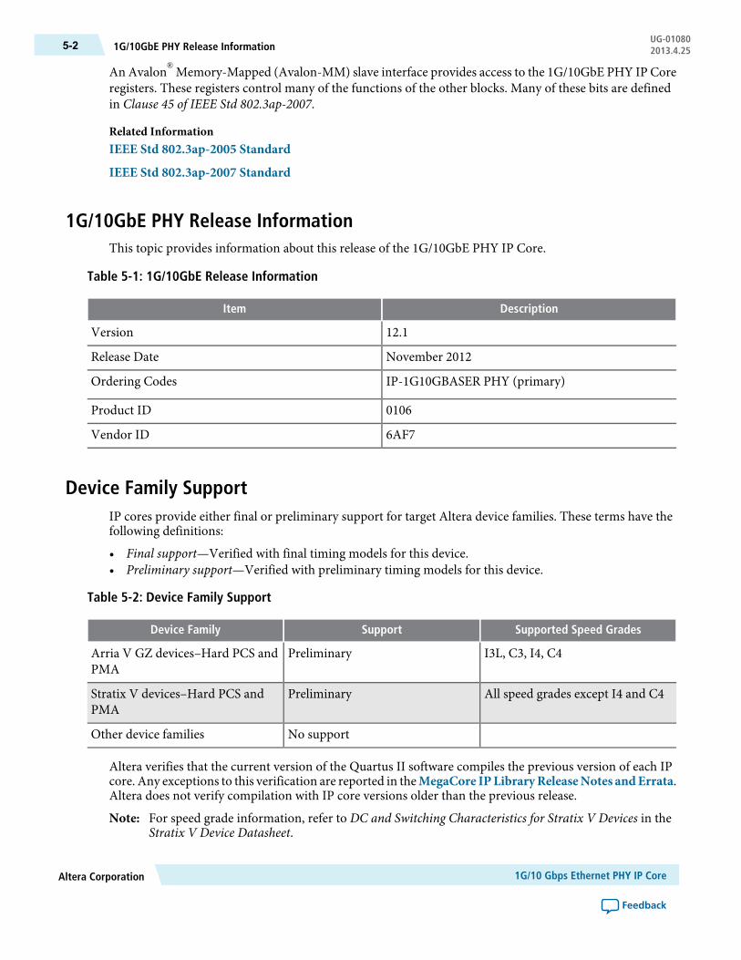
An Avalon®Memory-Mapped (Avalon-MM) slave interface provides access to the 1G/10GbE PHY IP Coreregisters. These registers control many of the functions of the other blocks. Many of these bits are definedin Clause 45 of IEEE Std 802.3ap-2007.
Related InformationIEEE Std 802.3ap-2005 Standard
IEEE Std 802.3ap-2007 Standard
1G/10GbE PHY Release InformationThis topic provides information about this release of the 1G/10GbE PHY IP Core.
Table 5-1: 1G/10GbE Release Information
DescriptionItem
12.1Version
November 2012Release Date
IP-1G10GBASER PHY (primary)Ordering Codes
0106Product ID
6AF7Vendor ID
Device Family SupportIP cores provide either final or preliminary support for target Altera device families. These terms have thefollowing definitions:
• Final support—Verified with final timing models for this device.• Preliminary support—Verified with preliminary timing models for this device.
Table 5-2: Device Family Support
Supported Speed GradesSupportDevice Family
I3L, C3, I4, C4PreliminaryArria V GZ devices–Hard PCS andPMA
All speed grades except I4 and C4PreliminaryStratix V devices–Hard PCS andPMA
No supportOther device families
Altera verifies that the current version of the Quartus II software compiles the previous version of each IPcore. Any exceptions to this verification are reported in theMegaCore IPLibraryReleaseNotes andErrata.Altera does not verify compilation with IP core versions older than the previous release.
For speed grade information, refer to DC and Switching Characteristics for Stratix V Devices in theStratix V Device Datasheet.
Note:
1G/10 Gbps Ethernet PHY IP CoreAltera Corporation
Feedback
UG-010801G/10GbE PHY Release Information5-2 2013.4.25

Related InformationStratix V Device Datasheet
1G/10GbE PHY Performance and Resource UtilizationThis topic provides performance and resource utilization for the IP core inArria VGZ and Stratix V devices.
The following table shows the typical expected resource utilization for selected configurations using thecurrent version of theQuartus II software targeting a StratixVGT (5SGTMC7K2F40C2) device. The numbersof ALMs and logic registers are rounded up to the nearest 100. Resource utilization numbers reflect changesto the resource utilization reporting starting in the Quartus II software v12.1 release 28 nm device familiesand upcoming device families.
Table 5-3: 1G/10GbE PHY Performance and Resource Utilization
Logic RegistersM20K MemoryALMsPHY Module Options
60003001GbE/10GbE - 1GbE only
70004001GbE/10GbE - 1GbE onlywith Sequencer
2000410001GbE/10GbE -1GbE/10GbE with 1588
2000411001GbE/10GbE -1GbE/10GbE with 1588and Sequencer
Parameterizing the 1G/10GbE PHYThe 1G/10GbE PHY IP Core is available for the Arria V GZ and Stratix V device families. The IP variantallows you specify either the Backplane-KR or 1Gb/10Gb Ethernet variant. When you select theBackplane-KR variant, the Link Training (LT) and Auto Negotiation (AN) tabs appear. The 1Gb/10GbEthernet variant (1G/10GbE) does not implement LT and AN parameters.
Complete the following steps to configure the 1G/10GbEPHY IPCore in theMegaWizard Plug-InManager:
1. For Which device family will you be using?, select Arria V GZ or Stratix V from the list.2. Click Installed Plug-Ins > Interfaces > Ethernet> 1G10GbE and 10BASE-KR PHY v12.1.3. Use the tabs on the MegaWizard Plug-In Manager to select the options required for the protocol.4. Refer to the topics listed as Related Links to understand and specify 1G/10GbE parameters:5. Click Finish to generate your parameterized 1G/10GbE PHY IP Core.
Altera Corporation1G/10 Gbps Ethernet PHY IP Core
Feedback
5-31G/10GbE PHY Performance and Resource UtilizationUG-010802013.4.25

Related Information1GbE Parameters on page 4-6
1G/10GbE Speed Detection Parameters on page 4-7
1G/10GbE PHY Analog Parameters on page 4-8
1GbE ParametersThe 1GbE parameters allow you to specify options for the 1GbE mode.
Table 5-4: 1Gb Ethernet Parameters
DescriptionOptionsParameter Name
When you turn this optionOn, the core includes theGMIIinterface and related logic.
On/OffEnable 1Gb Ethernetprotocol
When you turn this optionOn, the core includes the SGMIIclock and rate adaptation logic for the PCS. You must turnthis option On if you enable 1G mode.
On/OffEnable SGMII bridge logic
When you turn this optionOn, the core includes amodulein the PCS to implement the IEEE 1588 Precision TimeProtocol.
On/OffEnable IEEE1588PrecisionTime Protocol
An optional 32-bit value that serves as a unique identifierfor a particular type of PCS. The identifier includes thefollowing components:
• Bits 3-24 of the Organizationally Unique Identifier(OUI) assigned by the IEEE
• 6-bit model number• 4-bit revision number
If unused, do not change the default value which is0x00000000.
32-bit valuePHY ID (32 bit)
This is an optional 16-bit value identifies the PHY coreversion.
16-bit valuePHYCore version (16 bits)
Specifies the clock frequency for the 1GBASE-KR PHY IPCore. The default is 125 MHz.
125.00 MHz
62.50 MHz
Reference clock frequency
1G/10GbE Speed Detection ParametersBy selecting the Enable automatic speed detection option in the Megawizard, the PHY IP implementsParallel Detect as described in the Ethernet specification.
Selecting the speed detection option gives the PHY ability to detect to link partners that support 1G/10GbEbut have disabled Auto-Negotiation. If you turn On the Enable automatic speed detection parameter, thePHY includes the sequencer block. During Auto-Negotiation, if AN cannot detect Differential ManchesterEncoding (DME) pages from link partner, the Sequencer reconfigures to 1GE and 10GEmodes (Speed/Paralleldetection) until it detects a valid 1G or 10GbE pattern.
1G/10 Gbps Ethernet PHY IP CoreAltera Corporation
Feedback
UG-010801GbE Parameters5-4 2013.4.25
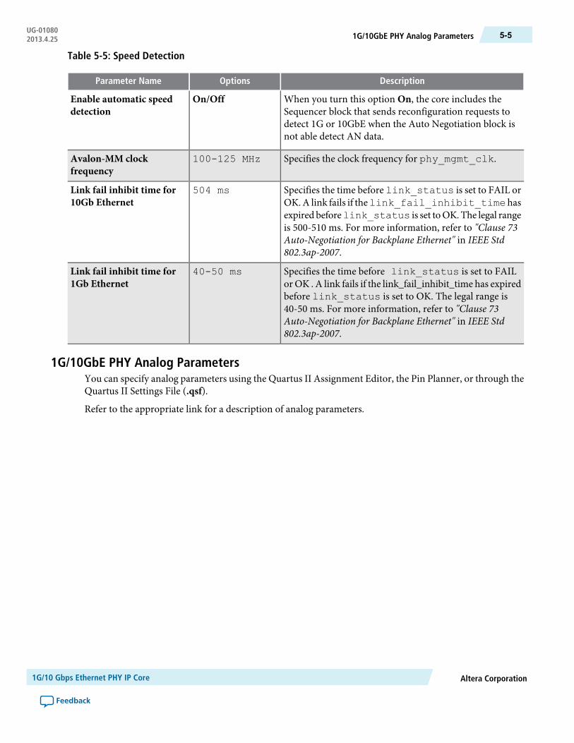
Table 5-5: Speed Detection
DescriptionOptionsParameter Name
When you turn this option On, the core includes theSequencer block that sends reconfiguration requests todetect 1G or 10GbE when the Auto Negotiation block isnot able detect AN data.
On/OffEnable automatic speeddetection
Specifies the clock frequency for phy_mgmt_clk.100-125 MHzAvalon-MM clockfrequency
Specifies the time before link_status is set to FAIL orOK.A link fails if thelink_fail_inhibit_timehasexpired beforelink_status is set toOK.The legal rangeis 500-510 ms. For more information, refer to "Clause 73Auto-Negotiation for Backplane Ethernet" in IEEE Std802.3ap-2007.
504 msLink fail inhibit time for10Gb Ethernet
Specifies the time before link_status is set to FAILor OK . A link fails if the link_fail_inhibit_time has expiredbefore link_status is set to OK. The legal range is40-50 ms. For more information, refer to "Clause 73Auto-Negotiation for Backplane Ethernet" in IEEE Std802.3ap-2007.
40-50 msLink fail inhibit time for1Gb Ethernet
1G/10GbE PHY Analog ParametersYou can specify analog parameters using the Quartus II Assignment Editor, the Pin Planner, or through theQuartus II Settings File (.qsf).
Refer to the appropriate link for a description of analog parameters.
Altera Corporation1G/10 Gbps Ethernet PHY IP Core
Feedback
5-51G/10GbE PHY Analog ParametersUG-010802013.4.25
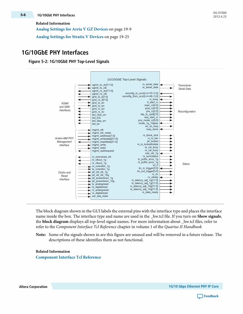
Related InformationAnalog Settings for Arria V GZ Devices on page 19-9
Analog Settings for Stratix V Devices on page 19-25
1G/10GbE PHY InterfacesFigure 5-2: 1G/10GbE PHY Top-Level Signals
xgmii_tx_dc[71:0]xgmii_tx_clkxgmii_rx_dc[71:0]xgmii_rx_clkgmii_tx_d[7:0]gmii_rx_d[7:0]gmii_tx_engmii_tx_errgmii_rx_errgmii_rx_dvled_char_errled_linkled_disp_errled_an
mgmt_clkmgmt_clk_resetmgmt_address[7:0]mgmt_writedata[31:0]mgmt_readdata[31:0]mgmt_writemgmt_readmgmt_waitrequest
rx_recovered_clktx_clkout_1grx_clkout_1grx_coreclkin_1gtx_coreclkin_1gpll_ref_clk_1gpll_ref_clk_10gpll_powerdown_1gpll_powerdown_10gtx_analogresettx_digitalresetrx_analogresetrx_digitalresetusr_seq_reset
1G/10GbE Top-Level Signals
Reconfiguration
rx_serial_datatx_serial_data
reconfig_to_xcvr[(<n>70-1):0]reconfig_from_xcvr[(<n>46-1):0]
rc_busylt_start_rc
main_rc[5:0]post_rc[4:0]pre_rc[3:0]
tap_to_upd[2:0]seq_start_rc
pcs_mode_rc[5:0]mode_1g_10gbar
en_lcl_rxeqrxeq_done
rx_block_lockrx_hi_berpll_locked
rx_is_lockedtodatatx_cal_busyrx_cal_busycalc_clk_1g
rx_syncstatustx_pcfifo_error_1grx_pcfifo_error_1g
lcl_rftm_in_trigger[3:0]
tm_out_trigger[3:0]rx_rlv
rx_clksliprx_latency_adj_1g[11:0]tx_latency_adj_1g[11:0]
rx_latency_adj_10g[11:0]tx_latency_adj_10g[11:0]
rx_data_ready
TransceiverSerial Data
XGMIIand GMIIInterfaces
Avalon-MM PHYManagementInterface
Clocks andReset
Interface
Status
The block diagram shown in the GUI labels the external pins with the interface type and places the interfacename inside the box. The interface type and name are used in the _hw.tcl file. If you turn on Show signals,the block diagram displays all top-level signal names. For more information about _hw.tcl files, refer torefer to the Component Interface Tcl Reference chapter in volume 1 of the Quartus II Handbook
Some of the signals shown in are this figure are unused and will be removed in a future release. Thedescriptions of these identifies them as not functional.
Note:
Related InformationComponent Interface Tcl Reference
1G/10 Gbps Ethernet PHY IP CoreAltera Corporation
Feedback
UG-010801G/10GbE PHY Interfaces5-6 2013.4.25

1G/10GbE PHY Clock and Reset InterfacesThis topic illustrates the 1G/10GbE PHY clock and reset connectivity and describes the clock and resetsignals.
Use the Transceiver PHY Reset Controller IP Core to automatically control the transceiver reset sequence.This reset controller also has manual overrides for the TX and RX analog and digital circuits to allow youto reset individual channels upon reconfiguration.
If you instantiate multiple channels within a transceiver bank they share TX PLLs. If a reset is applied to thisPLL, it will affect all channels. Altera recommends leaving the TX PLL free-running after the start-up resetsequence is completed. After a channel is reconfigured you can simply reset the digital portions of thatspecific channel instead of going through the entire reset sequence. For more information about reset, referto the "Transceiver PHY Reset IP Core" chapter in the Altera Transceiver PHY IP Core User Guide.
Phy_mgmt_clk_reset is the Avalon-MM reset signal. Phy_mgmt_clk_reset is also an input tothe Transceiver PHY Reset Controller IP Core which is a separately instantiated module not included in the1G/10GbE and 10GBASE-KR variants. The Transceiver PHY Reset Controller IP Core resets the TX PLLand RX analog circuits and the TX and RX digital circuits. When complete, the Reset Controller asserts thetx_ready and rx_ready signals.
The following figure provides an overview of the clocking for this core.
Figure 5-3: Clocks for Standard and 10G PCS and TX PLLs
xgmii_rx_clk156.25 MHz
xgmii_tx_clk156.25 MHz
Native PHY
Stratix V STDRX PCS
Stratix VTX PMAtx_coreclkin_1g
125 MHz
Stratix VRX PMA
TX PLL
TX PLL
40
rx_pld_clk rx_pma_clk
TX serial data8GMII TX Data
72XGMII TX Data & Cntl
RX data
40 TX data
40
TX data
serial data
pll_ref_clk_10g644.53125 MHz
or322.265625 MHz
pll_ref_clk_1g125 MHz
or62.5 MHz
Stratix V STDTX PCS
tx_pld_clk tx_pma_clk
8GMII RX Data
pll_ref_clk_10g
72XGMII RX Data & Cntl recovered clk257.8125 MHz
rx_coreclkin_1g125 MHz
Stratix V 10GRX PCS
rx_pld_clk rx_pma_clk
Stratix V 10GTX PCS
tx_pld_clk tx_pma_clkfractional
PLL
(instantiateseparately)
GIGEPCS
GIGEPCS
The following table describes the clock and reset signals.
Table 5-6: Clock and Reset Signals
DescriptionDirectionSignal Name
The RX clock which is recovered from the received data. Youcan use this clock as a reference to lock an external clock source.Its frequency is 125 or 156.25 MHz.
Outputrx_recovered_clk
Altera Corporation1G/10 Gbps Ethernet PHY IP Core
Feedback
5-71G/10GbE PHY Clock and Reset InterfacesUG-010802013.4.25

DescriptionDirectionSignal Name
GMII TX clock for the 1G TX parallel data source interface.The frequency is 125 MHz.
Outputtx_clkout_1g
GMII RX clock for the 1G RX parallel data source interface.The frequency is 125 MHz.
Outputrx_clkout_1g
Clock to drive the read side of the RX phase compensationFIFO in the Standard PCS. The frequency is 125 MHz.
Inputrx_coreclkin_1g
Clock to drive the write side of the TX phase compensationFIFO in the Standard PCS. The frequency is 125 MHz.
Inputtx_coreclkin_1g
Reference clock for the PMA block for the 1G mode. Itsfrequency is 125 or 62.5 MHz.
Inputpll_ref_clk_1g
Reference clock for the PMA block in 10G mode. Its frequencyis 644.53125 or 322.265625 MHz.
Inputpll_ref_clk_10g
Resets the 1Gb TX PLLs.Inputpll_powerdown_1g
Resets the 10Gb TX PLLs.Inputpll_powerdown_10g
Resets the analog TX portion of the transceiver PHY.Inputtx_analogreset
Resets the digital TX portion of the transceiver PHY.Inputtx_digitalreset
Resets the analog RX portion of the transceiver PHY.Inputrx_analogreset
Resets the digital RX portion of the transceiver PHY.Inputrx_digitalreset
Resets the sequencer.Inputusr_seq_rest
1G/10GbE PHY Data InterfacesThe following table describes the signals in the XGMII and GMII interfaces. The MAC drives the TX XGMIIand GMII signals to the 1G/10GbE PHY. The 1G/10GbE PHY drives the RX XGMII or GMII signals to theMAC.
Table 5-7: SGMII and GMII Signals
DescriptionDirectionSignal Name
1G/10GbE XGMII Data Interface
XGMII data and control for 8 lanes. Each lane consists of 8 bitsof data and 1 bit of control.
Inputxgmii_tx_dc[71:0]
Clock for single data rate (SDR) XGMII TX interface to theMAC. It should connect to xgmii_rx_clk. The frequency is156.25 MHz. Driven from the MAC. When you enable 1588the frequency is 257.8125 MHz.
Inputxgmii_tx_clk
RX XGMII data and control for 8 lanes. Each lane consists of8 bits of data and 1 bit of control.
Outputxgmii_rx_dc[71:0]
1G/10 Gbps Ethernet PHY IP CoreAltera Corporation
Feedback
UG-010801G/10GbE PHY Data Interfaces5-8 2013.4.25

DescriptionDirectionSignal Name
Clock for SDRXGMII RX interface to theMAC.The frequencyis 156.25MHz.When you enable 1588 the frequency is 257.8125MHz.
Inputxgmii_rx_clk
1G/10GbE GMII Data Interface
TXdata for 1Gmode. Synchronized to tx_clkout_1g clock. TheTX PCS 8B/10B module encodes this data which is sent to linkpartner.
Inputgmii_tx_d[7:0]
RX data for 1G mode. Synchronized to rx_clkout_1g clock.The RX PCS 8B/10B decoders decodes this data and sends itto the MAC.
Outputgmii_rx_d[7:0]
When asserted, indicates the start of a new frame. It shouldremain asserted until the last byte of data on the frame is presenton gmii_tx_d.
Inputgmii_tx_en
When asserted, indicates an error. May be asserted at any timeduring a frame transfer to indicate an error in that frame.
Inputgmii_tx_err
When asserted, indicates an error. May be asserted at any timeduring a frame transfer to indicate an error in that frame.
Outputgmii_rx_err
When asserted, indicates the start of a new frame. It remainsasserted until the last byte of data on the frame is present ongmii_rx_d.
Outputgmii_rx_dv
10-bit character error. Asserted for one rx_clkout_1g cyclewhen an erroneous 10-bit character is detected.
Outputled_char_err
When asserted, indicates successful link synchronization.Outputled_link
Disparity error signal indicating a 10-bit running disparityerror. Asserted for one rx_clkout_1g cycle when adisparity error is detected. A running disparity error indicatesthat more than the previous and perhaps the current receivedgroup had an error.
Outputled_disp_err
Clause 37 Auto-negotiation status. The PCS function assertsthis signal when auto-negotiation completes.
Outputled_an
1G/10GbE PHY XGMII Mapping to Standard SDR XGMII DataThis topic shows how the 72-bit TX and RX XGMII data buses map to the standard SDR XGMII interface.
The 72-bit TX XGMII data bus format is different than the standard SDR XGMII interface. The followingtable shows the mapping of this non-standard format to the standard SDR XGMII interface
Table 5-8: TX XGMII Mapping to Standard SDR XGMII Interface
DescriptionSDR XGMII Signal NameSignal Name
Lane 0 dataxgmii_sdr_data[7:0]xgmii_tx_dc[7:0]
Altera Corporation1G/10 Gbps Ethernet PHY IP Core
Feedback
5-91G/10GbE PHY XGMII Mapping to Standard SDR XGMII DataUG-010802013.4.25

DescriptionSDR XGMII Signal NameSignal Name
Lane 0 controlxgmii_sdr_ctrl[0]xgmii_tx_dc[8]
Lane 1 dataxgmii_sdr_data[15:8]xgmii_tx_dc[16:9]
Lane 1 controlxgmii_sdr_ctrl[1]xgmii_tx_dc[17]
Lane 2 dataxgmii_sdr_data[23:16]xgmii_tx_dc[25:18]
Lane 2 controlxgmii_sdr_ctrl[2]xgmii_tx_dc[26]
Lane 3 dataxgmii_sdr_data[31:24]xgmii_tx_dc[34:27]
Lane 3 controlxgmii_sdr_ctrl[3]xgmii_tx_dc[35]
Lane 4 dataxgmii_sdr_data[39:32]xgmii_tx_dc[43:36]
Lane 4 controlxgmii_sdr_ctrl[4]xgmii_tx_dc[44]
Lane 5 dataxgmii_sdr_data[47:40]xgmii_tx_dc[52:45]
Lane 5 controlxgmii_sdr_ctrl[5]xgmii_tx_dc[53]
Lane 6 dataxgmii_sdr_data[55:48]xgmii_tx_dc[61:54]
Lane 6 controlxgmii_sdr_ctrl[6]xgmii_tx_dc[62]
Lane 7 dataxgmii_sdr_data[63:56]xgmii_tx_dc[70:63]
Lane 7 controlxgmii_sdr_ctrl[7]xgmii_tx_dc[71]
The 72-bit RX XGMII data bus format is different from the standard SDR XGMII interface. The followingtable shows the mapping of this non-standard format to the standard SDR XGMII interface:
Table 5-9: RX XGMII Mapping to Standard SDR XGMII Interface
DescriptionXGMII Signal NameSignal Name
Lane 0 dataxgmii_sdr_data[7:0]xgmii_rx_dc[7:0]
Lane 0 controlxgmii_sdr_ctrl[0]xgmii_rx_dc[8]
Lane 1 dataxgmii_sdr_data[15:8]xgmii_rx_dc[16:9]
Lane 1 controlxgmii_sdr_ctrl[1]xgmii_rx_dc[17]
Lane 2 dataxgmii_sdr_data[23:16]xgmii_rx_dc[25:18]
Lane 2 controlxgmii_sdr_ctrl[2]xgmii_rx_dc[26]
Lane 3 dataxgmii_sdr_data[31:24]xgmii_rx_dc[34:27]
Lane 3 controlxgmii_sdr_ctrl[3]xgmii_rx_dc[35]
Lane 4 dataxgmii_sdr_data[39:32]xgmii_rx_dc[43:36]
Lane 4 controlxgmii_sdr_ctrl[4]xgmii_rx_dc[44]
Lane 5 dataxgmii_sdr_data[47:40]xgmii_rx_dc[52:45]
Lane 5 controlxgmii_sdr_ctrl[5]xgmii_rx_dc[53]
Lane 6 dataxgmii_sdr_data[55:48]xgmii_rx_dc[61:54]
1G/10 Gbps Ethernet PHY IP CoreAltera Corporation
Feedback
UG-010801G/10GbE PHY XGMII Mapping to Standard SDR XGMII Data5-10 2013.4.25
DescriptionXGMII Signal NameSignal Name
Lane 6 controlxgmii_sdr_ctrl[6]xgmii_rx_dc[62]
Lane 7 dataxgmii_sdr_data[63:56]xgmii_rx_dc[70:63]
Lane 7 controlxgmii_sdr_ctrl[7]xgmii_rx_dc[71]
1G/10GbE PHY Serial Data InterfaceThis topic describes the serial data interface.
DescriptionDirectionSignal Name
RX serial input dataInputrx_serial_data
TX serial output dataOutputtx_serial_data
1G/10GbE Control and Status InterfacesThe 1G/10GbE XGMII and GMII interface signals drive data to and from PHY.
Table 5-10: Control and Status Signals
DescriptionDirectionSignal Name
Asserted to indicate that the block synchronizer has establishedsynchronization.
Outputrx_block_lock
Asserted by the BER monitor block to indicate a Sync Headerhigh bit error rate greater than 10-4.
Outputrx_hi_ber
When asserted, indicates the TX PLL is locked.Outputpll_locked
When asserted, indicates the RX channel is locked to inputdata.
Outputrx_is_lockedtodata
When asserted, indicates that theTX channel is being calibrated.Outputtx_cal_busy
When asserted, indicates that theRX channel is being calibrated.Outputrx_cal_busy
This clock is used for calculating the latency of the soft 1G PCSblock. This clock is only required for when you enable 1588 in1G mode.
Inputcalc_clk_1g
When asserted, indicates the word aligner has aligned to inincoming word alignment pattern.
Outputrx_sync_status
When asserted, indicates that the Standard PCS TX phasecompensation FIFO is full.
Outputtx_pcfifo_error_1g
When asserted, indicates that the Standard PCS RX phasecompensation FIFO is full.
Outputrx_pcfifo_error_1g
When asserted, indicates a Remote Fault (RF).The MAC sendsthis fault signal to its link partner. Bit D13 of the AutoNegotiation Advanced Remote Fault register(0xC2) records this error.
Inputlcl_rf
This signal is not functional in 1G/10Gbe mode. Tie to 1'b0.Inputtrn_in_trigger[3:0]
Altera Corporation1G/10 Gbps Ethernet PHY IP Core
Feedback
5-111G/10GbE PHY Serial Data InterfaceUG-010802013.4.25
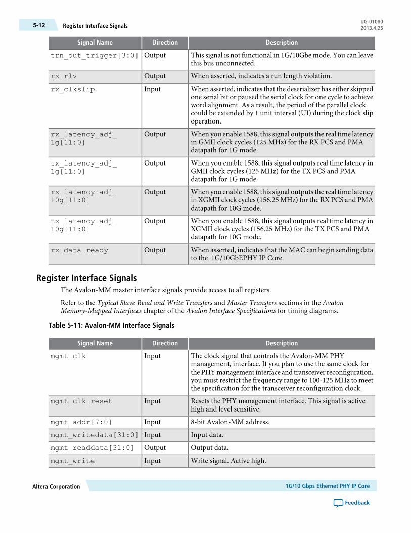
DescriptionDirectionSignal Name
This signal is not functional in 1G/10Gbe mode. You can leavethis bus unconnected.
Outputtrn_out_trigger[3:0]
When asserted, indicates a run length violation.Outputrx_rlv
When asserted, indicates that the deserializer has either skippedone serial bit or paused the serial clock for one cycle to achieveword alignment. As a result, the period of the parallel clockcould be extended by 1 unit interval (UI) during the clock slipoperation.
Inputrx_clkslip
When you enable 1588, this signal outputs the real time latencyin GMII clock cycles (125 MHz) for the RX PCS and PMAdatapath for 1G mode.
Outputrx_latency_adj_1g[11:0]
When you enable 1588, this signal outputs real time latency inGMII clock cycles (125 MHz) for the TX PCS and PMAdatapath for 1G mode.
Outputtx_latency_adj_1g[11:0]
When you enable 1588, this signal outputs the real time latencyin XGMII clock cycles (156.25 MHz) for the RX PCS and PMAdatapath for 10G mode.
Outputrx_latency_adj_10g[11:0]
When you enable 1588, this signal outputs real time latency inXGMII clock cycles (156.25 MHz) for the TX PCS and PMAdatapath for 10G mode.
Outputtx_latency_adj_10g[11:0]
When asserted, indicates that the MAC can begin sending datato the 1G/10GbEPHY IP Core.
Outputrx_data_ready
Register Interface SignalsThe Avalon-MM master interface signals provide access to all registers.
Refer to the Typical Slave Read and Write Transfers and Master Transfers sections in the AvalonMemory-Mapped Interfaces chapter of the Avalon Interface Specifications for timing diagrams.
Table 5-11: Avalon-MM Interface Signals
DescriptionDirectionSignal Name
The clock signal that controls the Avalon-MM PHYmanagement, interface. If you plan to use the same clock forthePHYmanagement interface and transceiver reconfiguration,you must restrict the frequency range to 100-125 MHz to meetthe specification for the transceiver reconfiguration clock.
Inputmgmt_clk
Resets the PHY management interface. This signal is activehigh and level sensitive.
Inputmgmt_clk_reset
8-bit Avalon-MM address.Inputmgmt_addr[7:0]
Input data.Inputmgmt_writedata[31:0]
Output data.Outputmgmt_readdata[31:0]
Write signal. Active high.Inputmgmt_write
1G/10 Gbps Ethernet PHY IP CoreAltera Corporation
Feedback
UG-01080Register Interface Signals5-12 2013.4.25

DescriptionDirectionSignal Name
Read signal. Active high.Inputmgmt_read
When asserted, indicates that the Avalon-MM slave interfaceis unable to respond to a read or write request. When asserted,control signals to the Avalon-MM slave interface must remainconstant.
Outputmgmt_waitrequest
Related InformationAvalon Interface Specifications
1G/10GbE PHY Register DefinitionsYou can access the 1G/10GbE registers using the Avalon-MM PHY management interface with wordaddresses and a 32-bit embedded processor. A single address space provides access to all registers.
Unless otherwise indicated, the default value of all registers is 0.Note:
Writing to reserved or undefined register addresses may have undefined side effects.Note:
Table 5-12: 1G/10GbE Register Definitions
DescriptionNameR/WBitAddr
When set to 1, resets the sequencer. This bit must beused in conjunction with SEQ Force Mode[2:0] . Thisreset self clears.
Reset SEQRW0
0xB0
Reserved.1
When set to 1, disables the Link Fault timer. When setto 0, the Link Fault timer is enabled.
Disable LF TimerRW2
Forces the sequencer to a specific protocol. Allows youto change speeds if you have turned on Enableautomatic speed detection in theGUI. Youmust writethe Reset SEQ bit to 1 for the Force to take effect. Thefollowing encodings are defined:
• 3'b000: No force• 3'b001: GigE• 3'b010: Reserved• 3'b011: Reserved• 3'b100: 10GBASE-R• 3'b101: Reserved• Others: Reserved
SEQ ForceMode[2:0]
RW6:4
When asserted, the sequencer is indicating that the linkis ready.
SEQ Link ReadyRO00xB1
Related InformationAvalon Interface Specifications
Altera Corporation1G/10 Gbps Ethernet PHY IP Core
Feedback
5-131G/10GbE PHY Register DefinitionsUG-010802013.4.25
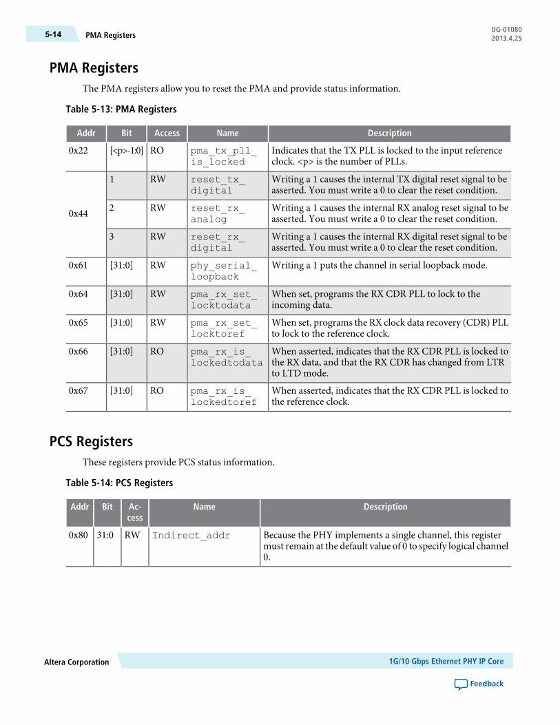
PMA RegistersThe PMA registers allow you to reset the PMA and provide status information.
Table 5-13: PMA Registers
DescriptionNameAccessBitAddr
Indicates that the TX PLL is locked to the input referenceclock. <p> is the number of PLLs.
pma_tx_pll_is_locked
RO[<p>-1:0]0x22
Writing a 1 causes the internal TX digital reset signal to beasserted. You must write a 0 to clear the reset condition.
reset_tx_digital
RW1
0x44 Writing a 1 causes the internal RX analog reset signal to beasserted. You must write a 0 to clear the reset condition.
reset_rx_analog
RW2
Writing a 1 causes the internal RX digital reset signal to beasserted. You must write a 0 to clear the reset condition.
reset_rx_digital
RW3
Writing a 1 puts the channel in serial loopback mode.phy_serial_loopback
RW[31:0]0x61
When set, programs the RX CDR PLL to lock to theincoming data.
pma_rx_set_locktodata
RW[31:0]0x64
When set, programs the RX clock data recovery (CDR) PLLto lock to the reference clock.
pma_rx_set_locktoref
RW[31:0]0x65
When asserted, indicates that the RX CDR PLL is locked tothe RX data, and that the RX CDR has changed from LTRto LTD mode.
pma_rx_is_lockedtodata
RO[31:0]0x66
When asserted, indicates that the RX CDR PLL is locked tothe reference clock.
pma_rx_is_lockedtoref
RO[31:0]0x67
PCS RegistersThese registers provide PCS status information.
Table 5-14: PCS Registers
DescriptionNameAc-cess
BitAddr
Because the PHY implements a single channel, this registermust remain at the default value of 0 to specify logical channel0.
Indirect_addrRW31:00x80
1G/10 Gbps Ethernet PHY IP CoreAltera Corporation
Feedback
UG-01080PMA Registers5-14 2013.4.25
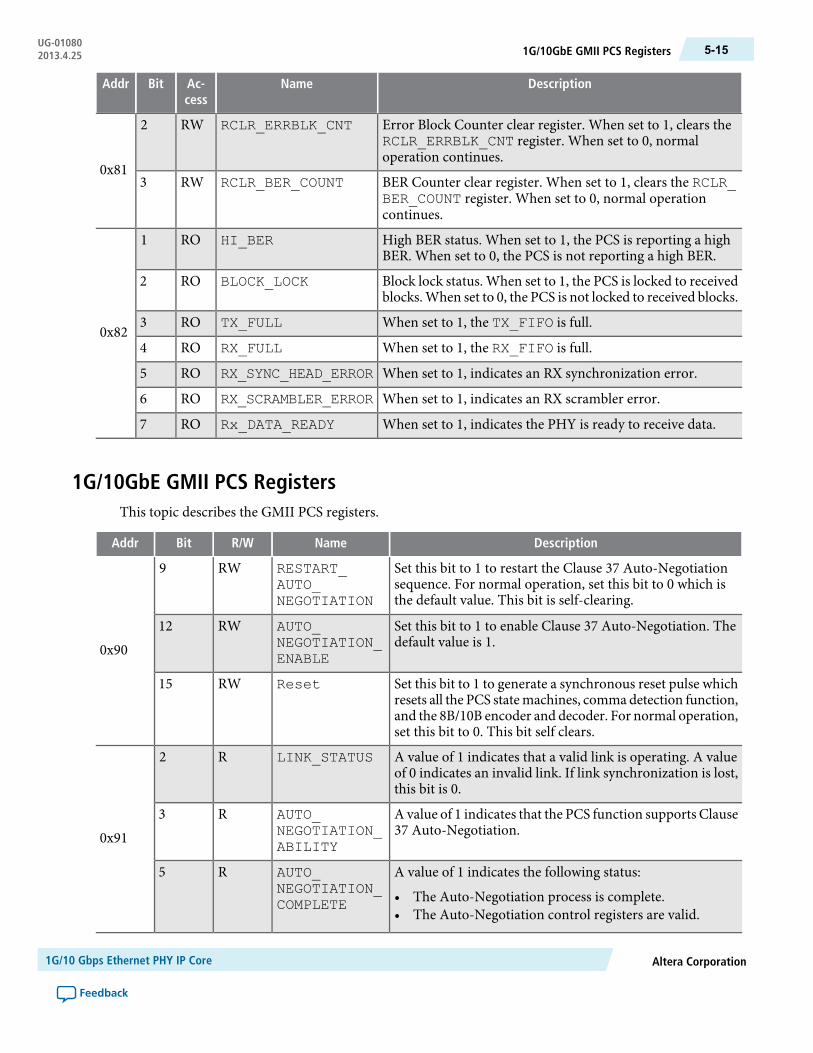
DescriptionNameAc-cess
BitAddr
Error Block Counter clear register. When set to 1, clears theRCLR_ERRBLK_CNT register. When set to 0, normaloperation continues.
RCLR_ERRBLK_CNTRW2
0x81BER Counter clear register. When set to 1, clears the RCLR_BER_COUNT register. When set to 0, normal operationcontinues.
RCLR_BER_COUNTRW3
High BER status. When set to 1, the PCS is reporting a highBER. When set to 0, the PCS is not reporting a high BER.
HI_BERRO1
0x82
Block lock status. When set to 1, the PCS is locked to receivedblocks. When set to 0, the PCS is not locked to received blocks.
BLOCK_LOCKRO2
When set to 1, the TX_FIFO is full.TX_FULLRO3
When set to 1, the RX_FIFO is full.RX_FULLRO4
When set to 1, indicates an RX synchronization error.RX_SYNC_HEAD_ERRORRO5
When set to 1, indicates an RX scrambler error.RX_SCRAMBLER_ERRORRO6
When set to 1, indicates the PHY is ready to receive data.Rx_DATA_READYRO7
1G/10GbE GMII PCS RegistersThis topic describes the GMII PCS registers.
DescriptionNameR/WBitAddr
Set this bit to 1 to restart the Clause 37 Auto-Negotiationsequence. For normal operation, set this bit to 0 which isthe default value. This bit is self-clearing.
RESTART_AUTO_NEGOTIATION
RW9
0x90
Set this bit to 1 to enable Clause 37 Auto-Negotiation. Thedefault value is 1.
AUTO_NEGOTIATION_ENABLE
RW12
Set this bit to 1 to generate a synchronous reset pulse whichresets all the PCS statemachines, commadetection function,and the 8B/10B encoder and decoder. For normal operation,set this bit to 0. This bit self clears.
ResetRW15
A value of 1 indicates that a valid link is operating. A valueof 0 indicates an invalid link. If link synchronization is lost,this bit is 0.
LINK_STATUSR2
0x91
A value of 1 indicates that the PCS function supports Clause37 Auto-Negotiation.
AUTO_NEGOTIATION_ABILITY
R3
A value of 1 indicates the following status:
• The Auto-Negotiation process is complete.• The Auto-Negotiation control registers are valid.
AUTO_NEGOTIATION_COMPLETE
R5
Altera Corporation1G/10 Gbps Ethernet PHY IP Core
Feedback
5-151G/10GbE GMII PCS RegistersUG-010802013.4.25
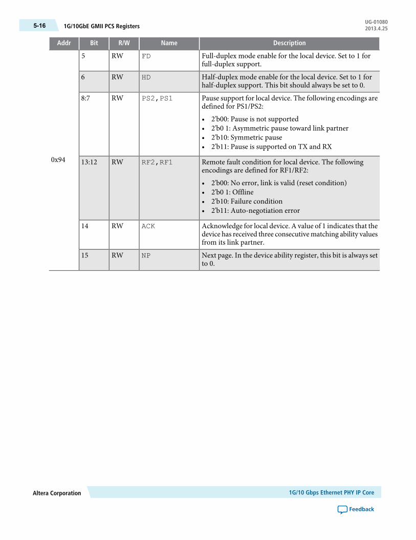
DescriptionNameR/WBitAddr
Full-duplex mode enable for the local device. Set to 1 forfull-duplex support.
FDRW5
0x94
Half-duplex mode enable for the local device. Set to 1 forhalf-duplex support. This bit should always be set to 0.
HDRW6
Pause support for local device. The following encodings aredefined for PS1/PS2:
• 2'b00: Pause is not supported• 2'b0 1: Asymmetric pause toward link partner• 2'b10: Symmetric pause• 2'b11: Pause is supported on TX and RX
PS2,PS1RW8:7
Remote fault condition for local device. The followingencodings are defined for RF1/RF2:
• 2'b00: No error, link is valid (reset condition)• 2'b0 1: Offline• 2'b10: Failure condition• 2'b11: Auto-negotiation error
RF2,RF1RW13:12
Acknowledge for local device. A value of 1 indicates that thedevice has received three consecutivematching ability valuesfrom its link partner.
ACKRW14
Next page. In the device ability register, this bit is always setto 0.
NPRW15
1G/10 Gbps Ethernet PHY IP CoreAltera Corporation
Feedback
UG-010801G/10GbE GMII PCS Registers5-16 2013.4.25

DescriptionNameR/WBitAddr
Full-duplexmode enable for the link partner. This bit shouldalways be 1 because only full duplex is supported.
FDR5
0x95
Half-duplex mode enable for the link partner. A value of 1indicates support for half duplex. This bit should always be0 because half-duplex mode is not supported.
HDR6
Specifies pause support for link partner. The followingencodings are defined for PS1/PS2:
• 2'b00: Pause is not supported• 2'b0 1: Asymmetric pause toward link partner• 2'b10: Symmetric pause• 2'b11: Pause is supported on TX and RX
PS2,PS1R8:7
Remote fault condition for link partner. The followingencodings are defined for RF1/RF2:
• 2'b00: No error, link is valid (reset condition)• 2'b0 1: Offline• 2'b10: Failure condition• 2'b11: Auto-negotiation error
RF2,RF1R13:12
Acknowledge for link partner. A value of 1 indicates thatthe device has received three consecutive matching abilityvalues from its link partner.
ACKR14
Next page. In link partner register. When set to 0, the linkpartner has a Next Page to send. When set to 1, the linkpartner does not a Next Page. Next Page is not supported inAuto Negotiation.
NPR15
Set set to 1, indicates that the link partner supports autonegotiation. The default value is 0.
LINK_PARTNER_AUTO_NEGOTIATION_ABLE
R0
0x96A value of 1 indicates that a newpage has been receivedwithnew partner ability available in the register partner ability.The default value is 0 when the system management agentperforms a read access.
PAGE_RECEIVER1
PMA RegistersThe PMA registers allow you to customize the TX and RX serial data interface.
Altera Corporation1G/10 Gbps Ethernet PHY IP Core
Feedback
5-17PMA RegistersUG-010802013.4.25
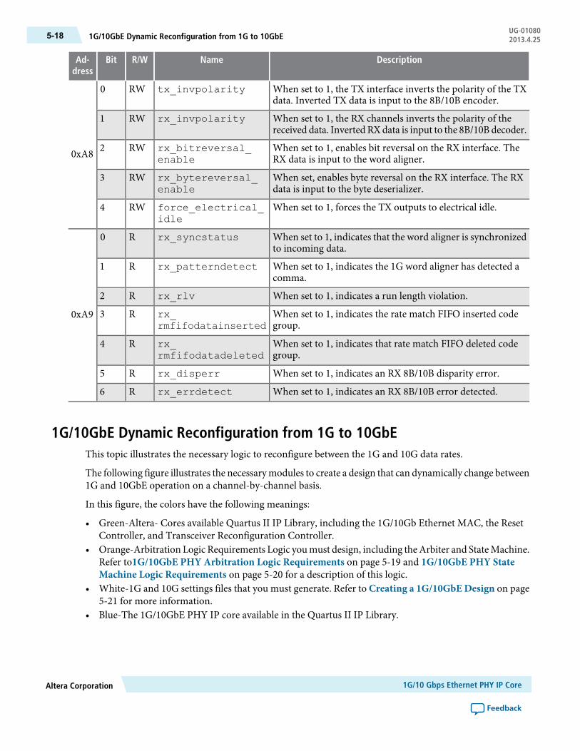
DescriptionNameR/WBitAd-dress
When set to 1, the TX interface inverts the polarity of the TXdata. Inverted TX data is input to the 8B/10B encoder.
tx_invpolarityRW0
0xA8
When set to 1, the RX channels inverts the polarity of thereceived data. Inverted RXdata is input to the 8B/10B decoder.
rx_invpolarityRW1
When set to 1, enables bit reversal on the RX interface. TheRX data is input to the word aligner.
rx_bitreversal_enable
RW2
When set, enables byte reversal on the RX interface. The RXdata is input to the byte deserializer.
rx_bytereversal_enable
RW3
When set to 1, forces the TX outputs to electrical idle.force_electrical_idle
RW4
When set to 1, indicates that the word aligner is synchronizedto incoming data.
rx_syncstatusR0
0xA9
When set to 1, indicates the 1G word aligner has detected acomma.
rx_patterndetectR1
When set to 1, indicates a run length violation.rx_rlvR2
When set to 1, indicates the rate match FIFO inserted codegroup.
rx_rmfifodatainserted
R3
When set to 1, indicates that rate match FIFO deleted codegroup.
rx_rmfifodatadeleted
R4
When set to 1, indicates an RX 8B/10B disparity error.rx_disperrR5
When set to 1, indicates an RX 8B/10B error detected.rx_errdetectR6
1G/10GbE Dynamic Reconfiguration from 1G to 10GbEThis topic illustrates the necessary logic to reconfigure between the 1G and 10G data rates.
The following figure illustrates the necessarymodules to create a design that can dynamically change between1G and 10GbE operation on a channel-by-channel basis.
In this figure, the colors have the following meanings:
• Green-Altera- Cores available Quartus II IP Library, including the 1G/10Gb Ethernet MAC, the ResetController, and Transceiver Reconfiguration Controller.
• Orange-Arbitration Logic Requirements Logic youmust design, including theArbiter and StateMachine.Refer to1G/10GbE PHY Arbitration Logic Requirements on page 5-19 and 1G/10GbE PHY StateMachine Logic Requirements on page 5-20 for a description of this logic.
• White-1G and 10G settings files that you must generate. Refer to Creating a 1G/10GbEDesign on page5-21 for more information.
• Blue-The 1G/10GbE PHY IP core available in the Quartus II IP Library.
1G/10 Gbps Ethernet PHY IP CoreAltera Corporation
Feedback
UG-010801G/10GbE Dynamic Reconfiguration from 1G to 10GbE5-18 2013.4.25

Figure 5-4: Block Diagram for Reconfiguration Example
1G/10GbEthernetMAC
Backplane-KR or 1G/10Gb Ethernet PHY MegaCore Function
Backplane-KR or 1G/10Gb Ethernet PHY MegaCore Function
Backplane-KR or 1G/10Gb Ethernet PHY MegaCore Function
Native PHY Hard IP
257.8MHz
40-b
40-bTX
SerialData
RXSerialData
322.265625 or644.53125Ref Clk
62.5 or 125Ref Clk
ATX/CMUTX PLLFor
10 GbE
ATX/CMUTX PLL
For 1 GbE
1.25 Gb/10.3125 GbHard PMA
LinkStatus
SequencerS
ResetController
StateMachineArbiter
rate change request
ack to user
rate changereq from user
TransceiverReconfigController
10 GbEthernetHard PCS
Cntl &Status
RX GMII Data
TX GMII Data@ 125 MHz
RX XGMII Data
TX XGMII Data
Shared Across Multiple ChannelsCan Share
Across MultipleChannels
@156.25 MHz
1 GIGEPCS
1G/10GbEthernetMAC1G/10Gb
EthernetMAC
1G
10G
1 GbEthernetStandardHard PCS
1G/10GbE PHY Arbitration Logic RequirementsThis topic describes the arbitration functionality that you must implement.
The arbiter should implement the following logic. You can modify this logic based on your systemrequirements:
1. Accept requests from the sequencer (if Enable automatic speed detection is turned On in the GUI) .Prioritize requests to meet system requirements. Requests should consist of the following two buses:
• Channel number—specifies the requested channel• Mode—specifies 1G or 10G mode for the corresponding channel
2. Select a channel for reconfiguration and send an ack/busy signal to the requestor. The requestor shoulddeassert its request signal when the ack/busy is received.
3. Pass the selected channel and rate information to the state machine for processing.4. Wait for a done signal from the state machine indicating that the reconfiguration process is complete
and it is ready to service another request.
Altera Corporation1G/10 Gbps Ethernet PHY IP Core
Feedback
5-191G/10GbE PHY Arbitration Logic RequirementsUG-010802013.4.25
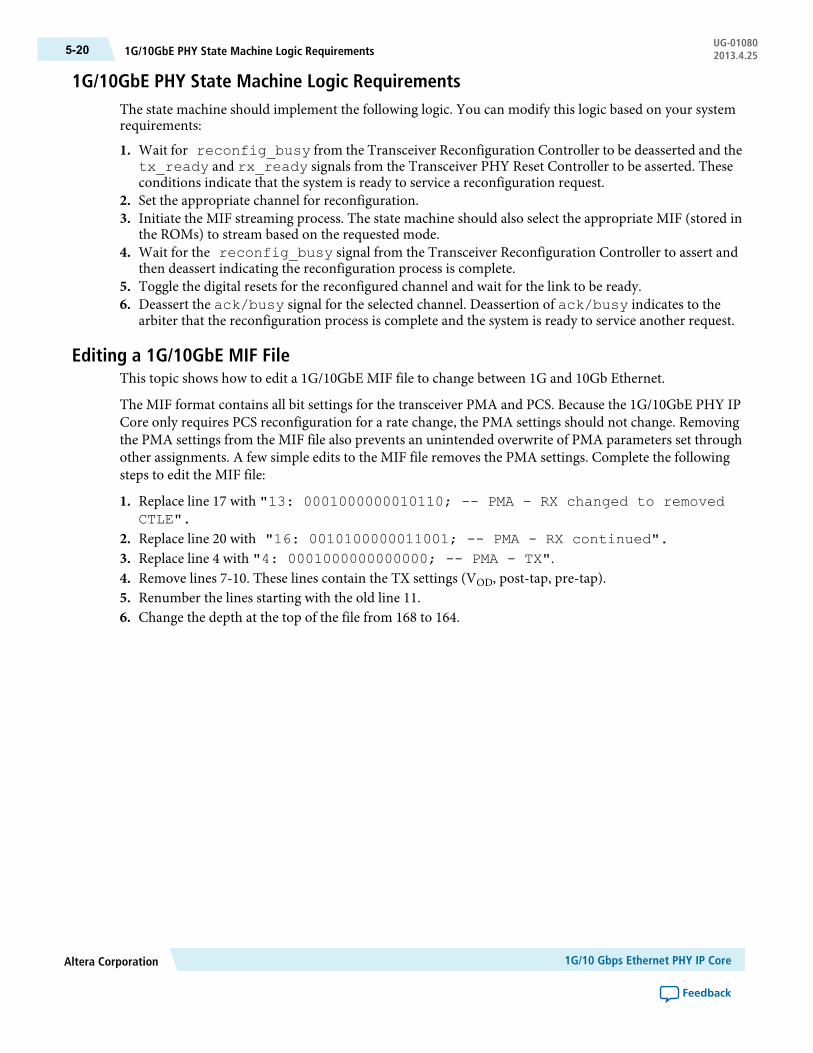
1G/10GbE PHY State Machine Logic RequirementsThe state machine should implement the following logic. You can modify this logic based on your systemrequirements:
1. Wait for reconfig_busy from the Transceiver Reconfiguration Controller to be deasserted and thetx_ready and rx_ready signals from the Transceiver PHY Reset Controller to be asserted. Theseconditions indicate that the system is ready to service a reconfiguration request.
2. Set the appropriate channel for reconfiguration.3. Initiate the MIF streaming process. The state machine should also select the appropriate MIF (stored in
the ROMs) to stream based on the requested mode.4. Wait for the reconfig_busy signal from the Transceiver Reconfiguration Controller to assert and
then deassert indicating the reconfiguration process is complete.5. Toggle the digital resets for the reconfigured channel and wait for the link to be ready.6. Deassert the ack/busy signal for the selected channel. Deassertion of ack/busy indicates to the
arbiter that the reconfiguration process is complete and the system is ready to service another request.
Editing a 1G/10GbE MIF FileThis topic shows how to edit a 1G/10GbE MIF file to change between 1G and 10Gb Ethernet.
The MIF format contains all bit settings for the transceiver PMA and PCS. Because the 1G/10GbE PHY IPCore only requires PCS reconfiguration for a rate change, the PMA settings should not change. Removingthe PMA settings from the MIF file also prevents an unintended overwrite of PMA parameters set throughother assignments. A few simple edits to the MIF file removes the PMA settings. Complete the followingsteps to edit the MIF file:
1. Replace line 17 with "13: 0001000000010110; -- PMA - RX changed to removedCTLE".
2. Replace line 20 with "16: 0010100000011001; -- PMA - RX continued".3. Replace line 4 with "4: 0001000000000000; -- PMA - TX".4. Remove lines 7-10. These lines contain the TX settings (VOD, post-tap, pre-tap).5. Renumber the lines starting with the old line 11.6. Change the depth at the top of the file from 168 to 164.
1G/10 Gbps Ethernet PHY IP CoreAltera Corporation
Feedback
UG-010801G/10GbE PHY State Machine Logic Requirements5-20 2013.4.25
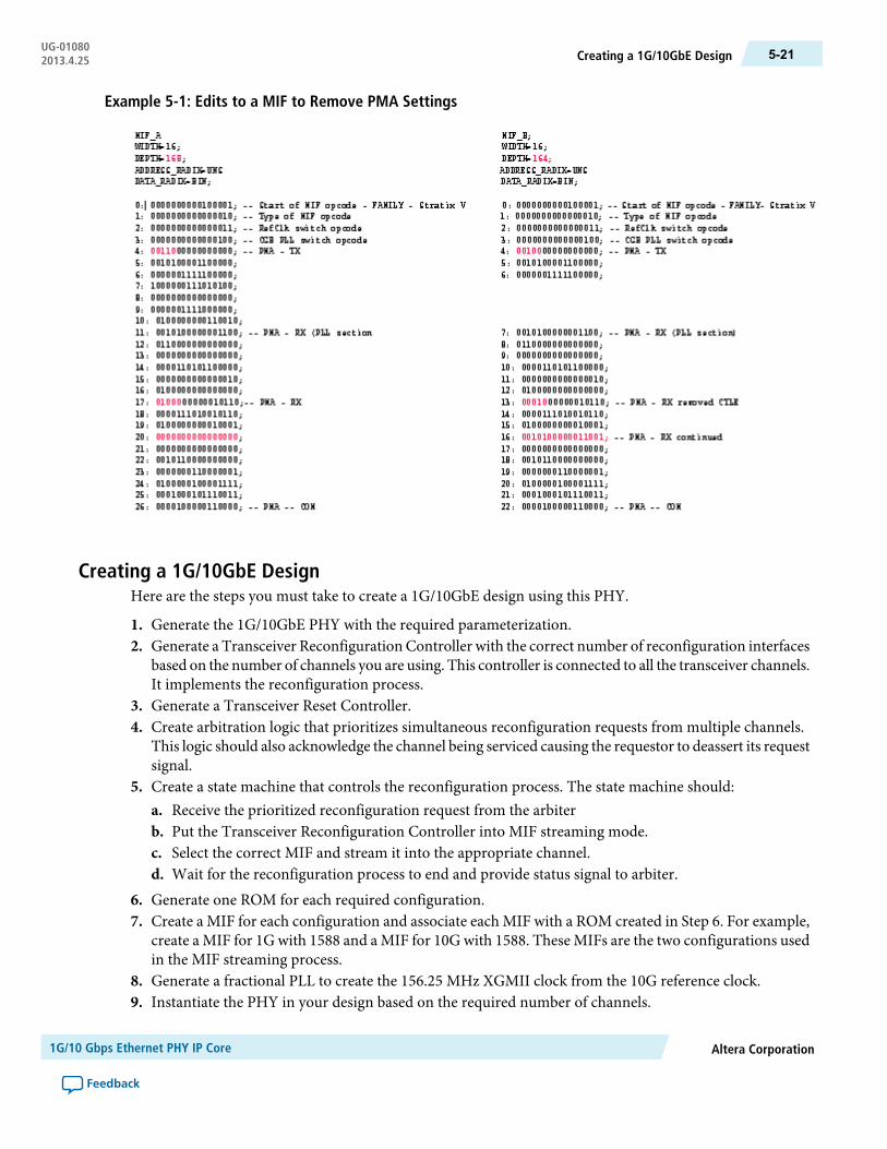
Example 5-1: Edits to a MIF to Remove PMA Settings
Creating a 1G/10GbE DesignHere are the steps you must take to create a 1G/10GbE design using this PHY.
1. Generate the 1G/10GbE PHY with the required parameterization.2. Generate a Transceiver Reconfiguration Controller with the correct number of reconfiguration interfaces
based on the number of channels you are using. This controller is connected to all the transceiver channels.It implements the reconfiguration process.
3. Generate a Transceiver Reset Controller.4. Create arbitration logic that prioritizes simultaneous reconfiguration requests from multiple channels.
This logic should also acknowledge the channel being serviced causing the requestor to deassert its requestsignal.
5. Create a state machine that controls the reconfiguration process. The state machine should:a. Receive the prioritized reconfiguration request from the arbiterb. Put the Transceiver Reconfiguration Controller into MIF streaming mode.c. Select the correct MIF and stream it into the appropriate channel.d. Wait for the reconfiguration process to end and provide status signal to arbiter.
6. Generate one ROM for each required configuration.7. Create a MIF for each configuration and associate each MIF with a ROM created in Step 6. For example,
create a MIF for 1G with 1588 and a MIF for 10G with 1588. These MIFs are the two configurations usedin the MIF streaming process.
8. Generate a fractional PLL to create the 156.25 MHz XGMII clock from the 10G reference clock.9. Instantiate the PHY in your design based on the required number of channels.
Altera Corporation1G/10 Gbps Ethernet PHY IP Core
Feedback
5-21Creating a 1G/10GbE DesignUG-010802013.4.25
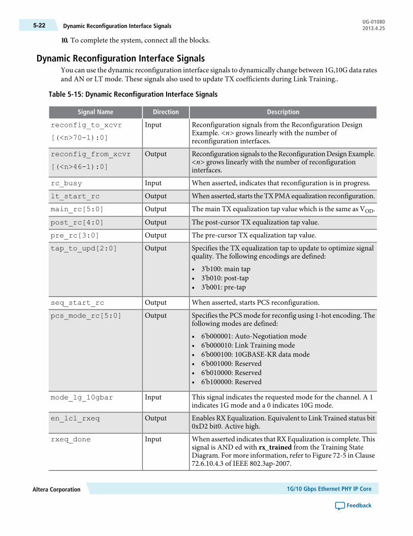
10. To complete the system, connect all the blocks.
Dynamic Reconfiguration Interface SignalsYou can use the dynamic reconfiguration interface signals to dynamically change between 1G,10Gdata ratesand AN or LT mode. These signals also used to update TX coefficients during Link Training..
Table 5-15: Dynamic Reconfiguration Interface Signals
DescriptionDirectionSignal Name
Reconfiguration signals from the Reconfiguration DesignExample. <n> grows linearly with the number ofreconfiguration interfaces.
Inputreconfig_to_xcvr
[(<n>70-1):0]
Reconfiguration signals to theReconfigurationDesignExample.<n> grows linearly with the number of reconfigurationinterfaces.
Outputreconfig_from_xcvr
[(<n>46-1):0]
When asserted, indicates that reconfiguration is in progress.Inputrc_busy
When asserted, starts theTXPMAequalization reconfiguration.Outputlt_start_rc
The main TX equalization tap value which is the same as VOD.Outputmain_rc[5:0]
The post-cursor TX equalization tap value.Outputpost_rc[4:0]
The pre-cursor TX equalization tap value.Outputpre_rc[3:0]
Specifies the TX equalization tap to update to optimize signalquality. The following encodings are defined:
• 3'b100: main tap• 3'b010: post-tap• 3'b001: pre-tap
Outputtap_to_upd[2:0]
When asserted, starts PCS reconfiguration.Outputseq_start_rc
Specifies the PCS mode for reconfig using 1-hot encoding. Thefollowing modes are defined:
• 6'b000001: Auto-Negotiation mode• 6'b000010: Link Training mode• 6'b000100: 10GBASE-KR data mode• 6'b001000: Reserved• 6'b010000: Reserved• 6'b100000: Reserved
Outputpcs_mode_rc[5:0]
This signal indicates the requested mode for the channel. A 1indicates 1G mode and a 0 indicates 10G mode.
Inputmode_1g_10gbar
Enables RX Equalization. Equivalent to Link Trained status bit0xD2 bit0. Active high.
Outputen_lcl_rxeq
When asserted indicates that RXEqualization is complete. Thissignal is AND ed with rx_trained from the Training StateDiagram. For more information, refer to Figure 72-5 in Clause72.6.10.4.3 of IEEE 802.3ap-2007.
Inputrxeq_done
1G/10 Gbps Ethernet PHY IP CoreAltera Corporation
Feedback
UG-01080Dynamic Reconfiguration Interface Signals5-22 2013.4.25
Design ExampleAltera provides a design example to assist you in integrating your Ethernet PHY IP into your completedesign.
The MAC and PHY design example instantiates the 1G/10GbE PHY IP along with the 1G/10G EthernetMAC and supporting logic. It is part of the Quartus II 12.1 installation and is located in the<quartus2_install_dir>/ip subdirectory. Formore information about this example design, refer to theEthernetMAC MegaCore Function User Guide
1G/10GbE PHY IP Core Simulation SupportThe 1G/10GbE PHY IP Core supports ModelSim Verilog and ModelSim VHDL, VCS Verilog, and VCSVHDL simulation. Stratix V devices also support NCSIM Verilog and NCSIM VHDL simulation. TheMegaWizard Plug-In Manager generates an IP functional simulation model when you press the Finishbutton.
1G/10GbE TimeQuest Timing ConstraintsTo pass timing analysis, you must decouple the clocks in different time domains. The necessary SynopsysDesignConstraints File (.sdc) timing constraints for the 1G/10GbEPHY IPCore are included in the top-levelwrapper file.
AcronymsThis table defines some commonly used Ethernet acronyms.
Table 5-16: Ethernet Acronyms
DefinitionAcronym
Auto-Negotiation in Ethernet as described in Clause 73 or of IEEE 802.3ap-2007.AN
Bit Error Rate.BER
Differential Manchester Encoding.DME
Forward error correction.FEC
Gigabit Media Independent Interface.GMII
Short hand notation for Backplane Ethernet with 64b/66b encoding.KR
Local Device.LD
Link training in backplane Ethernet Clause 72 for 10GBASE-KR and 40GBASE-KR4.LT
Link partner, to which the LD is connected.LP
Media Access Control.MAC
Media independent interface.MII
Open System Interconnection.OSI
Altera Corporation1G/10 Gbps Ethernet PHY IP Core
Feedback
5-23Design ExampleUG-010802013.4.25

DefinitionAcronym
Physical Coding Sublayer.PCS
Physical Layer in OSI 7-layer architecture, also in Altera device scope is: PCS + PMA.PHY
Physical Medium Attachment.PMA
Physical Medium Dependent.PMD
Serial Gigabit Media Independent Interface.SGMII
Wide Area Network.WAN
10 Gigabit Attachment Unit Interface.XAUI
1G/10 Gbps Ethernet PHY IP CoreAltera Corporation
Feedback
UG-01080Acronyms5-24 2013.4.25

6XAUI PHY IP Core
2013.4.25UG-01080 Subscribe Feedback
The Altera XAUI PHY IP Core implements the IEEE 802.3 Clause 48 specification to extend the operationaldistance of the XGMII interface and reduce the number of interface signals.
XAUI extends the physical separation possible between the 10Gbps EthernetMAC function and the Ethernetstandard PHY component to onemeter. TheXAUI IPCore accepts 72-bit data (single data rate–SDRXGMII)from the application layer at either 156.25 Mbps or 312.5 Mbps. The serial interface runs at either 4 × 3.125Gbps or 4 × 6.25 Gbps (DDR XAUI option).
Figure 6-1: XAUI PHY IP Core
XAUI IP Core
4 x 3.125 Gbps serialor
4 x 6.5 Gbps serial
Altera FPGA
Hard PMA
PCS
8B/10BWord AlignerPhase Comp
SDR XGMII72 bits @ 156.25 Mbps
or72 bits @ 312.5 Mbps
Avalon-MMControl & Status
4
4
For Stratix IV GX and GT devices, you can choose a hard XAUI physical coding sublayer (PCS) and physicalmedia attachment (PMA), or a soft XAUI PCS and PMA in low latency mode. You can also combine bothhard and soft PCS configurations in the same device, using all channels in a transceiver bank. The PCS isonly available in soft logic for Stratix V devices.
Formore detailed information about theXAUI transceiver channel datapath, clocking, and channel placement,refer to the “XAUI” section in the Transceiver Configurations in Stratix V Devices chapter of the Stratix VDevice Handbook.
Related InformationIEEE 802.3 Clause 48
Transceiver Configurations in Stratix V Devices
XAUI PHY Release InformationThis section provides information about this release of the XAUI PHY IP Core.
ISO9001:2008Registered
© 2013 Altera Corporation. All rights reserved. ALTERA, ARRIA, CYCLONE, HARDCOPY, MAX, MEGACORE, NIOS, QUARTUS and STRATIXwords and logos are trademarks of Altera Corporation and registered in the U.S. Patent and Trademark Office and in other countries. All other wordsand logos identified as trademarks or service marks are the property of their respective holders as described at www.altera.com/common/legal.html.Altera warrants performance of its semiconductor products to current specifications in accordance with Altera's standard warranty, but reserves theright to make changes to any products and services at any time without notice. Altera assumes no responsibility or liability arising out of the applicationor use of any information, product, or service described herein except as expressly agreed to in writing by Altera. Altera customers are advised toobtain the latest version of device specifications before relying on any published information and before placing orders for products or services.
www.altera.com
101 Innovation Drive, San Jose, CA 95134

Table 6-1: XAUI Release Information
DescriptionItem
12.0Version
November 2012Release Date
P-XAUIPCS (primary)–Soft PCS
IPR-XAUIPCS (renewal)–Soft PCS
Ordering Codes3
00D7Product ID
6AF7Vendor ID
XAUI PHY Device Family SupportThis section describes device family support for the IP core.
IP cores provide either final or preliminary support for target Altera device families. These terms have thefollowing definitions:
• Final support—Verified with final timing models for this device.
Preliminary support—Verified with preliminary timing models for this device.
Table 6-2: Device Family Support
SupportDevice Family
XAUI
FinalArria II GX -Hard PCS and PMA
FinalArria II GZ-Hard PCS and PMA
PreliminaryArria V GX-Soft PCS + PMA
PreliminaryArria V SoC-Soft PCS + PMA
PreliminaryArria V GZ devices-Soft PCS + PMA
FinalCyclone IV GX-Hard PCS and PMA
PreliminaryCyclone V-Soft PCS + PMA
PreliminaryCyclone V SoC-Soft PCS + hard PMA
FinalHardCopy® IV
FinalStratix IV GX and GT devices-Soft or hard PCS andPMA
PreliminaryStratix V devices-Soft PCS + PMA
3 No ordering codes or license files are required for the hard PCS and PMA PHY in Arria II GX, Cyclone IVGX, or Stratix IV GX or GT devices.
XAUI PHY IP CoreAltera Corporation
Feedback
UG-01080XAUI PHY Device Family Support6-2 2013.4.25
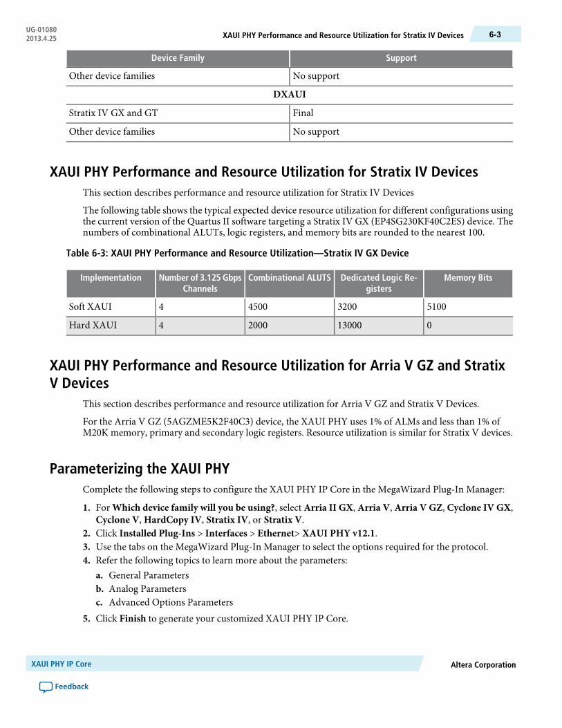
SupportDevice Family
No supportOther device families
DXAUI
FinalStratix IV GX and GT
No supportOther device families
XAUI PHY Performance and Resource Utilization for Stratix IV DevicesThis section describes performance and resource utilization for Stratix IV Devices
The following table shows the typical expected device resource utilization for different configurations usingthe current version of the Quartus II software targeting a Stratix IV GX (EP4SG230KF40C2ES) device. Thenumbers of combinational ALUTs, logic registers, and memory bits are rounded to the nearest 100.
Table 6-3: XAUI PHY Performance and Resource Utilization—Stratix IV GX Device
Memory BitsDedicated Logic Re-gisters
Combinational ALUTSNumber of 3.125 GbpsChannels
Implementation
5100320045004Soft XAUI
01300020004Hard XAUI
XAUI PHY Performance and Resource Utilization for Arria V GZ and StratixV Devices
This section describes performance and resource utilization for Arria V GZ and Stratix V Devices.
For the Arria V GZ (5AGZME5K2F40C3) device, the XAUI PHY uses 1% of ALMs and less than 1% ofM20K memory, primary and secondary logic registers. Resource utilization is similar for Stratix V devices.
Parameterizing the XAUI PHYComplete the following steps to configure the XAUI PHY IP Core in the MegaWizard Plug-In Manager:
1. For Which device family will you be using?, select Arria II GX, Arria V, Arria V GZ, Cyclone IV GX,Cyclone V, HardCopy IV, Stratix IV, or Stratix V.
2. Click Installed Plug-Ins > Interfaces > Ethernet> XAUI PHY v12.1.3. Use the tabs on the MegaWizard Plug-In Manager to select the options required for the protocol.4. Refer the following topics to learn more about the parameters:
a. General Parametersb. Analog Parametersc. Advanced Options Parameters
5. Click Finish to generate your customized XAUI PHY IP Core.
Altera CorporationXAUI PHY IP Core
Feedback
6-3XAUI PHY Performance and Resource Utilization for Stratix IV DevicesUG-010802013.4.25
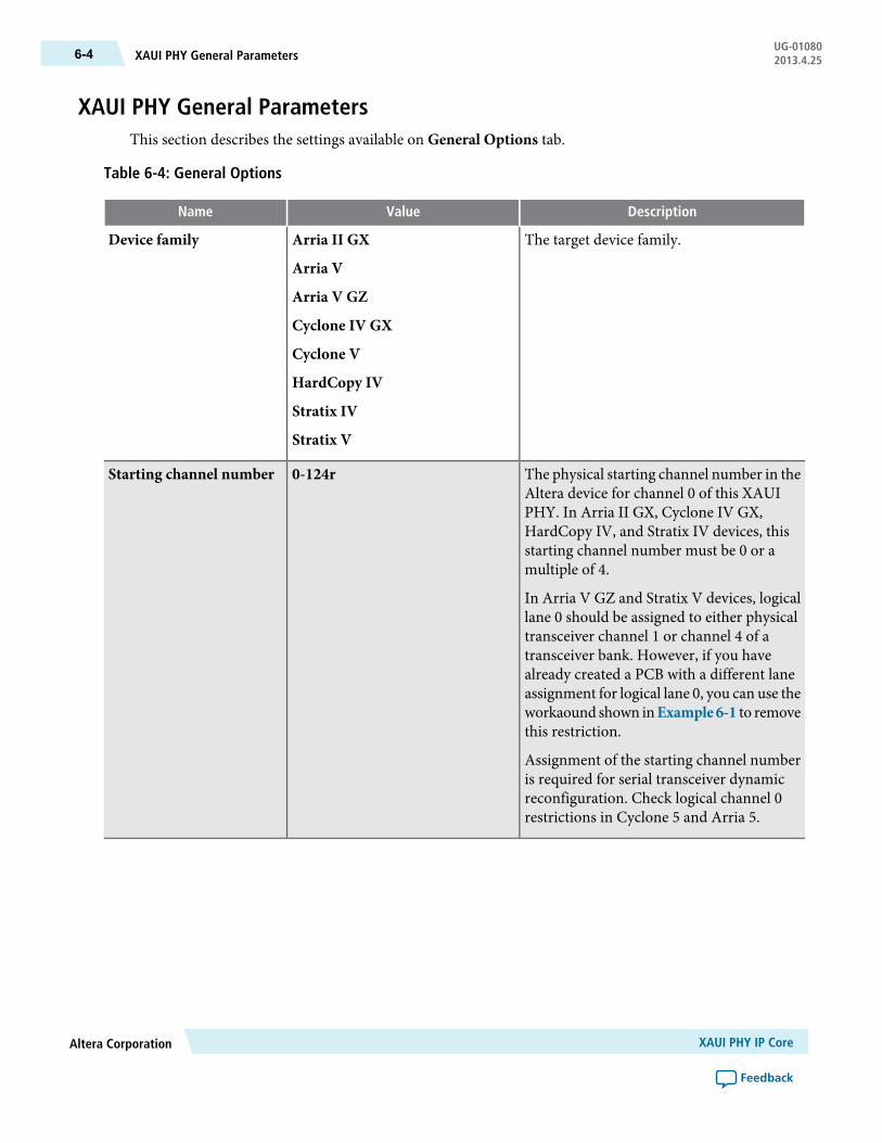
XAUI PHY General ParametersThis section describes the settings available on General Options tab.
Table 6-4: General Options
DescriptionValueName
The target device family.Arria II GX
Arria V
Arria V GZ
Cyclone IV GX
Cyclone V
HardCopy IV
Stratix IV
Stratix V
Device family
The physical starting channel number in theAltera device for channel 0 of this XAUIPHY. In Arria II GX, Cyclone IV GX,HardCopy IV, and Stratix IV devices, thisstarting channel number must be 0 or amultiple of 4.
In Arria V GZ and Stratix V devices, logicallane 0 should be assigned to either physicaltransceiver channel 1 or channel 4 of atransceiver bank. However, if you havealready created a PCB with a different laneassignment for logical lane 0, you can use theworkaound shown inExample6-1 to removethis restriction.
Assignment of the starting channel numberis required for serial transceiver dynamicreconfiguration. Check logical channel 0restrictions in Cyclone 5 and Arria 5.
0-124rStarting channel number
XAUI PHY IP CoreAltera Corporation
Feedback
UG-01080XAUI PHY General Parameters6-4 2013.4.25

DescriptionValueName
The following 3 interface types are available:
• Hard XAUI–Implements the PCS andPMA in hard logic. Available for Arria II,Cyclone IV, HardCopy IV, and StratixIV devices.
• Soft XAUI–Implements the PCS in softlogic and the PMA in hard logic.Available for HardCopy IV, Stratix IV,ArriaV, CycloneV, and StratixVdevices.
• DDRXAUI–Implements the PCS in softlogic and the PMA in hard logic. Both theapplication and serial interfaces run attwice the frequency of the Soft XAUIoptions. Available for HardCopy IVStratix IV devices.
All interface types include 4 channels.
Hard XAUI
Soft XAUI
DDR XAUII
XAUI interface type
Specifies the data rate.Device DependentData rate
You can select either the CMU or ATX PLL.The CMU PLL has a larger frequency rangethan theATXPLL. TheATXPLL is designedto improve jitter performance and achieveslower channel-to-channel skew; however, itsupports a narrower range of data rates andreference clock frequencies. Anotheradvantage of the ATX PLL is that it does notuse a transceiver channel, while the CMUPLL does. This parameter is available for thesoft PCS and DDR XAUI.
The ATX PLL is not available for all devices.
CMU
ATX
PLL type
The base data rate is the frequency of theclock input to the PLL. Select a base datarate that minimizes the number of PLLsrequired to generate all the clock s requiredfor data transmission. By selecting anappropriate base data rate, you can changedata rates by changing the divider used bythe clock generation block. This parameteris available for Stratix V devices.
1 × Lane rate
2 × Lane rate
4 × Lane rate
Base data rate
Specifies the number of XAUI interfaces.Only 1 is available in the current release.
1Number of XAUIinterfaces
Example 6-1 shows how to remove the restriction on logical lane 0 channel assignment in Stratix V devicesby redefining the pma_bonding_master parameter using the Quartus II Assignment Editor. In this example,
Altera CorporationXAUI PHY IP Core
Feedback
6-5XAUI PHY General ParametersUG-010802013.4.25

the pma_bonding_master was originally assigned to physical channel 1. (The original assignment could alsohave been to physical channel 4.) The to parameter reassigns the pma_bonding_master to theXAUI instancename shown in quotation marks. You must substitute the instance name from your design for the instancename shown in quotation marks
Example 6-1: Overriding Logical Lane 0 Channel Assignment Restrictions in Stratix V Devices
set_parameter -name pma_bonding_master "\"1\"" -to "<xauiinstancename>|sv_xcvr_xaui:alt_xaui_phy|sv_xcvr_low_latency_phy_nr:alt_pma_0|sv_xcvr_custom_native:sv_xcvr_custom_inst|sv_xcvr_native:gen.sv_xcvr_native_insts[0].gen_bonded_group.sv_xcvr_native_inst"
XAUI PHY Analog ParametersThis section describes the analog parameters for the IP core.
Click on the appropriate link to specify the analog options for your device:
• XAUIPHYAnalog Parameters forArria IIGX,Cyclone IVGX,HardCopy IV and Stratix IVDeviceson page 6-6
Related InformationAnalog Settings for Arria V Devices on page 19-2
Analog Settings for Arria V GZ Devices on page 19-9
Analog Settings for Cyclone V Devices on page 19-18
Analog Settings for Stratix V Devices on page 19-25
XAUI PHY Analog Parameters for Arria II GX, Cyclone IV GX, HardCopy IVand Stratix IV Devices
This section describes parameters for the Arria II GX, Cyclone IV GX, and Stratix IV devices; specify youranalog options on the Analog Options tab.
Table 6-5: PMA Analog Options
DescriptionValueName
Indicates the value of the terminationresistor for the transmitter.
OCT_85_OHMS
OCT_100_OHMS
OCT_120_OHMS
OCT_150_OHMS
Transmitter terminationresistance
Sets VOD for the various TX buffers.0–7Transmitter VOD control setting
XAUI PHY IP CoreAltera Corporation
Feedback
UG-01080XAUI PHY Analog Parameters6-6 2013.4.25
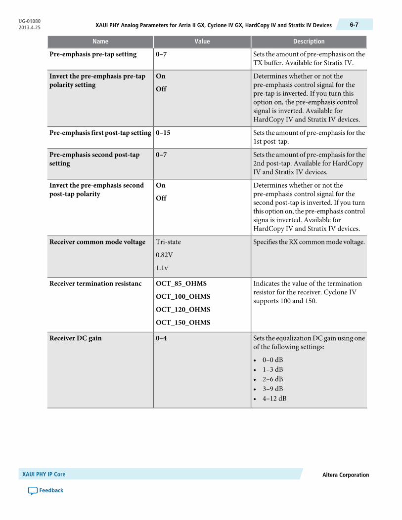
DescriptionValueName
Sets the amount of pre-emphasis on theTX buffer. Available for Stratix IV.
0–7Pre-emphasis pre-tap setting
Determines whether or not thepre-emphasis control signal for thepre-tap is inverted. If you turn thisoption on, the pre-emphasis controlsignal is inverted. Available forHardCopy IV and Stratix IV devices.
On
Off
Invert the pre-emphasis pre-tappolarity setting
Sets the amount of pre-emphasis for the1st post-tap.
0–15Pre-emphasis first post-tap setting
Sets the amount of pre-emphasis for the2nd post-tap. Available for HardCopyIV and Stratix IV devices.
0–7Pre-emphasis second post-tapsetting
Determines whether or not thepre-emphasis control signal for thesecond post-tap is inverted. If you turnthis option on, the pre-emphasis controlsigna is inverted. Available forHardCopy IV and Stratix IV devices.
On
Off
Invert the pre-emphasis secondpost-tap polarity
Specifies theRXcommonmode voltage.Tri-state
0.82V
1.1v
Receiver common mode voltage
Indicates the value of the terminationresistor for the receiver. Cyclone IVsupports 100 and 150.
OCT_85_OHMS
OCT_100_OHMS
OCT_120_OHMS
OCT_150_OHMS
Receiver termination resistanc
Sets the equalizationDC gain using oneof the following settings:
• 0–0 dB• 1–3 dB• 2–6 dB• 3–9 dB• 4–12 dB
0–4Receiver DC gain
Altera CorporationXAUI PHY IP Core
Feedback
6-7XAUI PHY Analog Parameters for Arria II GX, Cyclone IV GX, HardCopy IV and Stratix IV DevicesUG-010802013.4.25
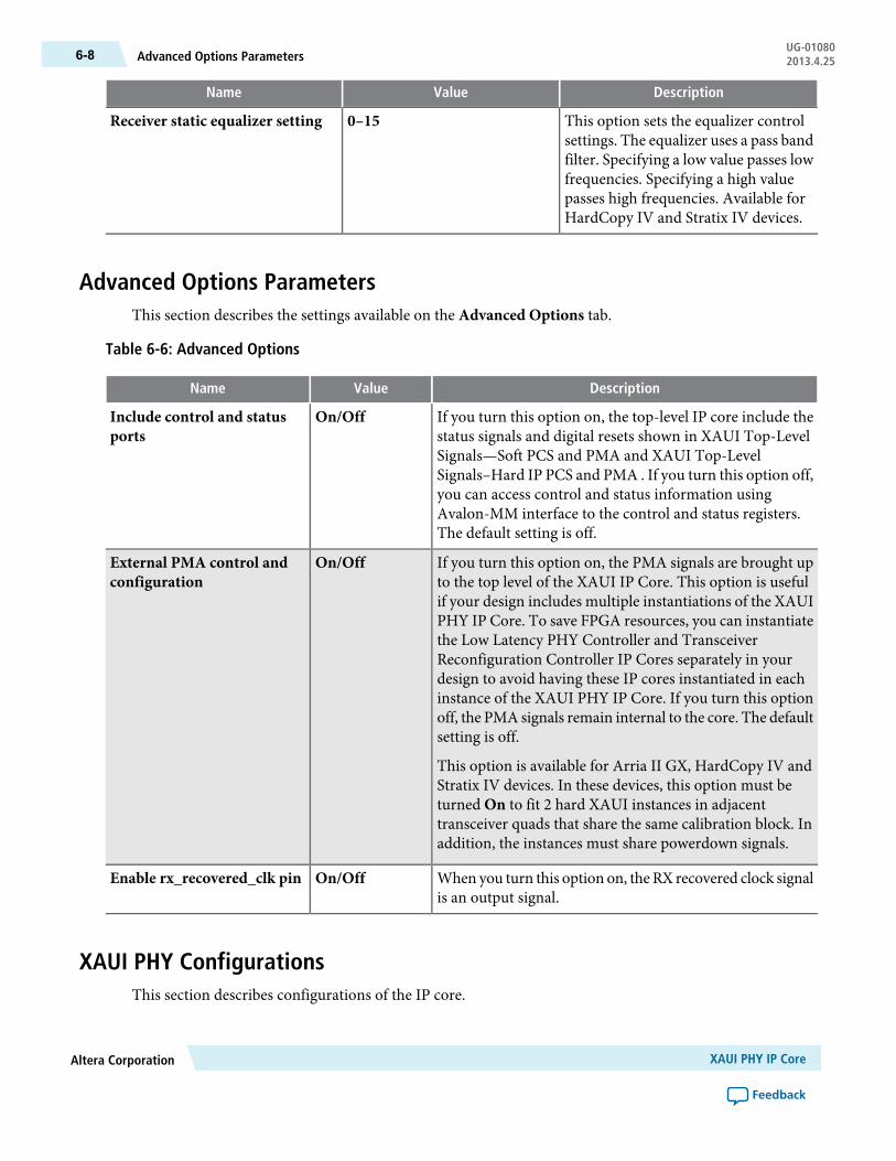
DescriptionValueName
This option sets the equalizer controlsettings. The equalizer uses a pass bandfilter. Specifying a low value passes lowfrequencies. Specifying a high valuepasses high frequencies. Available forHardCopy IV and Stratix IV devices.
0–15Receiver static equalizer setting
Advanced Options ParametersThis section describes the settings available on the Advanced Options tab.
Table 6-6: Advanced Options
DescriptionValueName
If you turn this option on, the top-level IP core include thestatus signals and digital resets shown in XAUI Top-LevelSignals—Soft PCS and PMA and XAUI Top-LevelSignals–Hard IP PCS and PMA . If you turn this option off,you can access control and status information usingAvalon-MM interface to the control and status registers.The default setting is off.
On/OffInclude control and statusports
If you turn this option on, the PMA signals are brought upto the top level of the XAUI IP Core. This option is usefulif your design includes multiple instantiations of the XAUIPHY IP Core. To save FPGA resources, you can instantiatethe Low Latency PHY Controller and TransceiverReconfiguration Controller IP Cores separately in yourdesign to avoid having these IP cores instantiated in eachinstance of the XAUI PHY IP Core. If you turn this optionoff, the PMA signals remain internal to the core. The defaultsetting is off.
This option is available for Arria II GX, HardCopy IV andStratix IV devices. In these devices, this option must beturned On to fit 2 hard XAUI instances in adjacenttransceiver quads that share the same calibration block. Inaddition, the instances must share powerdown signals.
On/OffExternal PMA control andconfiguration
When you turn this option on, the RX recovered clock signalis an output signal.
On/OffEnable rx_recovered_clk pin
XAUI PHY ConfigurationsThis section describes configurations of the IP core.
XAUI PHY IP CoreAltera Corporation
Feedback
UG-01080Advanced Options Parameters6-8 2013.4.25

The following figure illustrates one configuration of the XAUI IP Core. As this figure illustrates, if yourvariant includes a single instantiation of the XAUI IP Core, the transceiver reconfiguration control logic isincluded in the XAUI PHY IP Core. For Arria V, Cyclone V, and Stratix V devices the TransceiverReconfiguration Controller must always be external. Refer to Chapter 16, Transceiver ReconfigurationController IP Core for more information about this IP core. The Transceiver Reconfiguration Controller isalways separately instantiated in Stratix V and Arria V GZ devices.
Figure 6-2: XAUI PHY with Internal Transceiver Reconfiguration Control
SystemInterconnect
Fabric
Inter-leave
PCS
S
Alt_PMA
S
SLow Latency
Controller
STransceiver
ReconfigurationController
Transceiver Channel
Hard XAUI PHY
4 x 3.125 Gbps serial
to EmbeddedController
4
4
To MAC
SDR XGMII72 bits @ 156.25 Mbps
MAvalon-MM
PHYMgmt
S
PMA ChannelController
Related InformationTransceiver Reconfiguration Controller IP Core Overview on page 16-1
XAUI PHY PortsThis section describes the ports for the IP core.
Figure 6-3 illustrates the top-level signals of the XAUI PHY IP Core for the hard IP implementation. Thisvariant is available for Arria II GX, Cyclone IV GX, HardCopy IV and Stratix IV GX devices.Figure 6-4illustrates the top-level signals of the XAUI PHY IP Core for the soft IP implementation. With the exceptionof the optional signals available for debugging and the signals for dynamic reconfiguration of the transceivers,the top-level signals of the two variants is nearly identical. The DDR XAUI soft IP signals and behavior arethe same as the soft IP implementation.
Altera CorporationXAUI PHY IP Core
Feedback
6-9XAUI PHY PortsUG-010802013.4.25

The block diagram shown in theMegaWizard Plug-InManagerGUI labels the external pinswith the interfacetype and places the interface name inside the box. The interface type and name are used to define componentinterfaces in the _hw.tcl. If you turn on Show signals, the block diagram displays all top-level signal names.
For more information about _hw.tcl files refer to refer to the Component Interface Tcl Reference chapterin volume 1 of the Quartus II Handbook.
Figure 6-3: XAUI Top-Level Signals–Hard IP PCS and PMA
xgmii_tx_dc[71:0]xgmii_tx_clk
xgmii_rx_dc[71:0]xgmii_rx_clk
phy_mgmt_clkphy_mgmt_clk_resetphy_mgmt_address[8:0]phy_mgmt_writedata[31:0]phy_mgmt_readdata[31:0]phy_mgmt_writephy_mgmt_readphy_mgmt_waitrequest
pll_ref_clkrx_analogresetrx_digitalresettx_digitalreset
XAUI Top-Level Signals Hard IP Implementation
PMAChannelController
xaui_rx_serial_data[3:0]xaui_tx_serial_data[3:0]
rx_invpolarity[3:0]rx_set_locktodata[3:0]rx_is_lockedtodata[3:0]
rx_set_locktoref[3:0]rx_is_lockedtoref[3:0]
tx_invpolarity[3:0]rx_seriallpbken[3:0]
rx_channelaligned[3:0]rx_rmfifoempty[3:0]
rx_rmfifofull[3:0]rx_disperr[7:0]
rx_errdetect[7:0]rx_patterndetect[7:0]
rx_rmfifodatadeleted[7:0]rx_rmfifodatainserted[7:0]
rx_runningdisp[7:0]rx_syncstatus[7:0]
rx_phase_comp_fifo_error[3:0]tx_phase_comp_fifo_error[3:0]
rx_rlv[3:0]rx_recovered_clk[3:0]
reconfig_to_xcvr[3:0]reconfig_from_xcvr[16:0]
cal_blk_powerdowngxb_powerdownpll_powerdown
pll_lockedrx_readytx_ready
TransceiverSerial Data
Rx and TxStatus
All Optional
SDR Tx XGMII
SDR Rx XGMII
Avalon-MM PHYManagementInterface
ClockandReset
OptionalResets
TransceiverReconfiguration
(Optional)
Optional
The following figure illustrates the top-level signals of the XAUI PHY IPCore for the soft IP implementationfor both the single and DDR rates.
XAUI PHY IP CoreAltera Corporation
Feedback
UG-01080XAUI PHY Ports6-10 2013.4.25

Figure 6-4: XAUI Top-Level Signals—Soft PCS and PMA
xgmii_tx_dc[71:0]xgmii_tx_clk
xmii_rx_dc[71:0]xgmii_rx_clk
phy_mgmt_clkphy_mgmt_clk_resetphy_mgmt_address[8:0]phy_mgmt_writedata[31:0]phy_mgmt_readdata[31:0]phy_mgmt_writephy_mgmt_readphy_mgmt_waitrequest
pll_ref_clkrx_digitalresettx_digitalreset
XAUI Top-Level Signals
Rx StatusOptional
xaui_rx_serial_data[3:0]xaui_tx_serial_data[3:0]
rx_channelalignedrx_disperr[7:0]
rx_errdetect[7:0]rx_syncstatus[7:0]
reconfig_to_xcvr[(<n>70-1):0]reconfig_from_xcvr[(<n>46-1):0]
rx_recovered_clk[3:0]rx_readytx_ready
TransceiverSerial DataSDR TX XGMII
SDR RX XGMII
Avalon-MM PHYManagementInterface
ClocksandReset
Optional
DynamicReconfiguration
PMAChannelController
XAUI PHY Data InterfacesTheXAUIPCS interface to the FPGA fabric uses a SDRXGMII interface. This interface implements a simpleversion of Avalon-ST protocol. The interface does not include ready or valid signals; consequently, thesources always drive data and the sinks must always be ready to receive data.
Formore information about theAvalon-ST protocol, including timing diagrams, refer to theAvalon InterfaceSpecifications.
Depending on the parameters you choose, the application interface runs at either 156.25 Mbps or 312.5Mbps. At either frequency, data is only driven on the rising edge of clock. To meet the bandwidthrequirements, the datapath is eight bytes wide with eight control bits, instead of the standard four bytes ofdata and four bits of control. The XAUI IP Core treats the datapath as two, 32-bit data buses and includeslogic to interleave them, starting with the low-order bytes.
Figure 6-5: Interleaved SDR XGMII Data Mapping
Interleaved Result
Original XGMII Data
[63:56] [55:48] [47:40] [39:32] [31:24] [23:16] [15:8] [7:0]
[63:56] [31:24] [55:48] [23:16] [47:40] [15:8] [39:32] [7:0]
For the DDR XAUI variant, the start of control character (0xFB) is aligned to either byte 0 or byte 5.
Altera CorporationXAUI PHY IP Core
Feedback
6-11XAUI PHY Data InterfacesUG-010802013.4.25

Figure 6-6: Byte 0 Start of Frame Transmission Example
tx_clk
txc[7:0]
txd[7:0]
txd[31:8]
txd[39:32]
txd[55:40]
txd[63:56]
FF 01 00 F0 FF
start FB
AAAA
AA
frame data
frame data
frame data terminate FD
frame data
sfd AB frame data
AAAAAApreamble
preamble
preamble
Figure 6-7: Byte 4 Start of Frame Transmission Example
tx_clk
txc[7:0]
txd[7:0]
txd[23:8]
txd[31:24]
txd[39:32]
txd[55:40]
txd[63:56]
FF 1F 00 F8 FF
07 AA frame data
0707 AAAA
AAAA
AA
frame data
07 sfd AB frame data terminate FD
start FB frame data
frame data
frame data
preamble
preamble
preamble
preamble
preamble
Related InformationAvalon Interface Specifications
SDR XGMII TX InterfaceThis section describes the signals in the SDR TX XGMII interface.
Table 6-7: SDR TX XGMII Interface
DescriptionDirectionSignal Name
Contains 4 lanes of data and control for XGMII. Each laneconsists of 16 bits of data and 2 bits of control.
• Lane 0–[7:0]/[8], [43:36]/[44]• Lane 1–[16:9]/[17], [52:45]/[53]• Lane 2–[25:18]/[26], [61:54]/[62]• Lane 3–[34:27]/[35],[70:63]/[71]
Outputxgmii_tx_dc[71:0]
XAUI PHY IP CoreAltera Corporation
Feedback
UG-01080SDR XGMII TX Interface6-12 2013.4.25

DescriptionDirectionSignal Name
The XGMII SDR TX clock which runs at 156.25 MHz or 312.5for the DDR variant.
Inputxgmii_tx_clk
SDR XGMII RX InterfaceThis section describes the signals in the SDR RX XGMII interface.
Table 6-8: SDR RX XGMII Interface
DescriptionDirectionSignal Name
Contains 4 lanes of data and control for XGMII. Each laneconsists of 16 bits of data and 2 bits of control.
• Lane 0–[7:0]/[8], [43:36]/[44]• Lane 1–[16:9]/[17], [52:45]/[53]• Lane 2–[25:18]/[26], [61:54]/[62]• Lane 3–[34:27]/[35],[70:63]/[71]
Inputxgmii_rx_dc_[71:0]
The XGMII SDR RX clock which runs at 156.25 MHz.Outputxgmii_rx_clk
Transceiver Serial Data InterfaceThis section describes the signals in the XAUI transceiver serial data interface.
The XAUI transceiver serial data interface has four lanes of serial data for both the TX and RX interfaces.This interface runs at 3.125 GHz or 6.25 GHz depending on the variant you choose. There is no separateclock signal because it is encoded in the data.
Table 6-9: Serial Data Interface
DescriptionDirectionSignal Name
Serial input data.Inputxaui_rx_serial_data[3:0]
Serial output data.Outputxaui_tx_serial_data[3:0]
XAUI PHY Clocks, Reset, and Powerdown InterfacesThis section describes the clocks, reset, and oowerdown interfaces.
Altera CorporationXAUI PHY IP Core
Feedback
6-13SDR XGMII RX InterfaceUG-010802013.4.25

Figure 6-8: Clock Inputs and Outputs for IP Core with Hard PCS
XAUI Hard IP Core
4 x 3.125 Gbps serial
Hard PCStx_coreclk
rx_cruclkpll_inclk
coreclkoutxgmii_rx_clk
xgmii_tx_clk
pll_ref_clk
phy_mgmt_clk
4
4PMA
Figure 6-9: Clock Inputs and Outputs for IP Core with Soft PCS
XAUI Soft IP Core
4 x 3.125 Gbps serial
xgmii_rx_clk
xgmii_tx_clk
pll_ref_clk
phy_mgmt_clk
4
4Soft PCSpma_pll_inclk pma_tx_clkout tx_clkout
pma_rx_clkout
pll_ref_clk
sysclk
PMA
rx_recovered_clk
Table 6-10: Optional Clock and Reset Signals
DescriptionDirectionSignal Name
This is a 156.25 MHz reference clock that is used by theTX PLL and CDR logic.
Inputpll_ref_clk
This signal resets the analog CDR and deserializer logic inthe RX channel. It is only available in the hard IPimplementation.
Inputrx_analogreset
PCS RX digital reset signal.Inputrx_digitalreset
PCSTXdigital reset signal. If your design includes bondedTX PCS channels, refer to Timing Constraints for ResetSignals when Using Bonded PCS Channels for a SDCconstraint you must include in your design.
Inputtx_digitalreset
Refer to Transceiver Reconfiguration Controller for additional information about reset.
XAUI PHY IP CoreAltera Corporation
Feedback
UG-01080XAUI PHY Clocks, Reset, and Powerdown Interfaces6-14 2013.4.25

Related InformationTransceiver Reconfiguration Controller IP Core Overview on page 16-1
XAUI PHY PMA Channel Controller InterfaceThis sectiondescribes the signals in the PMA channel controller interface.
Table 6-11: PMA Channel Controller Signals
DescriptionDirectionSignal Name
Powers down the calibration block. A high-to-low transitionon this signal restarts calibration. Only available in Arria IIGX, HardCopy IV, and Stratix IV GX, and Stratix IV GTdevices.
Inputcal_blk_powerdown
When asserted, powers down the entire transceiver block.Only available in Arria II GX, HardCopy IV, and Stratix IVGX, and Stratix IV GT devices.
Inputgxb_powerdown
Powers down the CMU PLL. Only available in Arria II GX,HardCopy IV, and Stratix IV GX, and Stratix IV GT devices.
Inputpll_powerdown
Indicates CMU PLL is locked. Only available in Arria II GX,HardCopy IV, and Stratix IV GX, and Stratix IV GT devices.
Outputpll_locked
This is the RX clock which is recovered from the receiveddata stream.
Outputrx_recovered_clk[3:0]
Indicates PMA RX has exited the reset state and thetransceiver can receive data.
Outputrx_ready
Indicates PMA TX has exited the reset state and thetransceiver can transmit data.
Outputtx_ready
XAUI PHY Optional PMA Control and Status InterfaceYou can access the state of the optional PMAcontrol and status signals available in the soft IP implementationusing theAvalon-MMPHYManagement interface to read the control and status registers which are detailedin XAUI PHY IP Core Registers . However, in some cases, you may need to know the instantaneous valueof a signal to ensure correct functioning of the XAUI PHY. In such cases, you can include the required signalin the top-level module of your XAUI PHY IP Core.
Table 6-12: Optional Control and Status Signals—Soft IP Implementation
DescriptionDirectionSignal Name
When asserted, indicates that all 4 RX channelsare aligned.
Outputrx_channelaligned
Altera CorporationXAUI PHY IP Core
Feedback
6-15XAUI PHY PMA Channel Controller InterfaceUG-010802013.4.25

DescriptionDirectionSignal Name
Received 10-bit code or data group has a disparityerror. It is paired with rx_errdetect whichis also asserted when a disparity error occurs. Therx_disperr signal is 2 bits wide per channelfor a total of 8 bits per XAUI link.
Outputrx_disperr[7:0]
When asserted, indicates an 8B/10B code groupviolation. It is asserted if the received 10-bit codegroup has a code violation or disparity error. It isused along with the rx_disperr signal todifferentiate between a code violation error, adisparity error, or both. The rx_errdetectsignal is 2 bits wide per channel for a total of 8 bitsper XAUI link.
Outputrx_errdetect[7:0]
Synchronization indication. RX synchronizationis indicated on therx_syncstatusport of eachchannel. The rx_syncstatus signal is 2 bitsper channel for a total of 8 bits per hard XAUIlink. The rx_syncstatus signal is 1 bit perchannel for a total of 4 bits per soft XAUI link.
Outputrx_syncstatus[7:0]
When asserted indicates that the RX CDR PLL islocked to the incoming data.
Outputrx_is_lockedtodata[3:0]
When asserted indicates that the RX CDR PLL islocked to the reference clock.
Outputrx_is_lockedtoref[3:0]
This is the clock used for the SDR XGMIIinterface.
Outputtx_clk312_5
You can access the state of the PMA control and status signals available in the hard IP implementation usingthe Avalon-MM PHY Management interface to read the control and status registers which are detailed inXAUI PHY IP Core Registers. However, in some cases, you may need to know the instantaneous value of asignal to ensure correct functioning of the XAUI PHY. In such cases, you can include the required signal inthe top-level module of your XAUI PHY IP Core.
Table 6-13: Optional Control and Status Signals—Hard IP Implementation, Stratix IV GX Devices
DescriptionDirectionName
Dynamically reverse the polarity of every bit of the RX dataat the input of the word aligner.
Inputrx_invpolarity[3:0]
Force the CDR circuitry to lock to the received data.Inputrx_set_locktodata[3:0]
When asserted, indicates the RX channel is locked to inputdata.
Outputrx_is_lockedtodata[3:0]
Force the receiver CDR to lock to the phase and frequencyof the input reference clock.
Inputrx_set_locktoref[3:0]
XAUI PHY IP CoreAltera Corporation
Feedback
UG-01080XAUI PHY Optional PMA Control and Status Interface6-16 2013.4.25
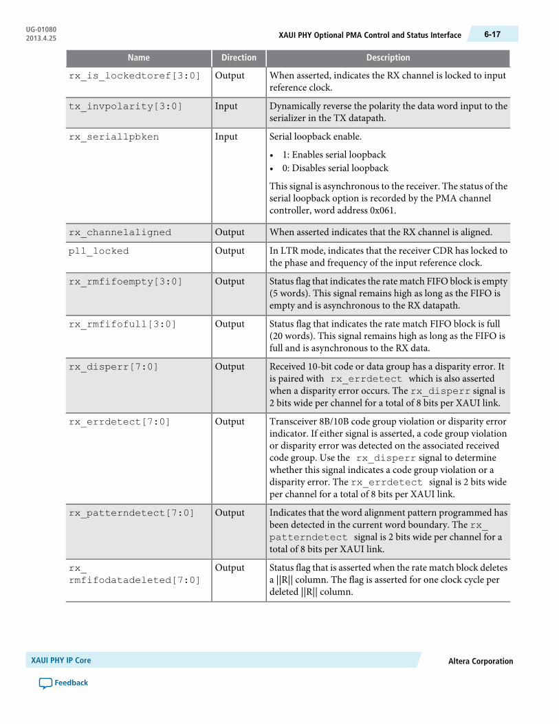
DescriptionDirectionName
When asserted, indicates the RX channel is locked to inputreference clock.
Outputrx_is_lockedtoref[3:0]
Dynamically reverse the polarity the data word input to theserializer in the TX datapath.
Inputtx_invpolarity[3:0]
Serial loopback enable.
• 1: Enables serial loopback• 0: Disables serial loopback
This signal is asynchronous to the receiver. The status of theserial loopback option is recorded by the PMA channelcontroller, word address 0x061.
Inputrx_seriallpbken
When asserted indicates that the RX channel is aligned.Outputrx_channelaligned
In LTR mode, indicates that the receiver CDR has locked tothe phase and frequency of the input reference clock.
Outputpll_locked
Status flag that indicates the rate match FIFO block is empty(5 words). This signal remains high as long as the FIFO isempty and is asynchronous to the RX datapath.
Outputrx_rmfifoempty[3:0]
Status flag that indicates the rate match FIFO block is full(20 words). This signal remains high as long as the FIFO isfull and is asynchronous to the RX data.
Outputrx_rmfifofull[3:0]
Received 10-bit code or data group has a disparity error. Itis paired with rx_errdetect which is also assertedwhen a disparity error occurs. The rx_disperr signal is2 bits wide per channel for a total of 8 bits per XAUI link.
Outputrx_disperr[7:0]
Transceiver 8B/10B code group violation or disparity errorindicator. If either signal is asserted, a code group violationor disparity error was detected on the associated receivedcode group. Use the rx_disperr signal to determinewhether this signal indicates a code group violation or adisparity error. The rx_errdetect signal is 2 bits wideper channel for a total of 8 bits per XAUI link.
Outputrx_errdetect[7:0]
Indicates that the word alignment pattern programmed hasbeen detected in the current word boundary. The rx_patterndetect signal is 2 bits wide per channel for atotal of 8 bits per XAUI link.
Outputrx_patterndetect[7:0]
Status flag that is asserted when the rate match block deletesa ||R|| column. The flag is asserted for one clock cycle perdeleted ||R|| column.
Outputrx_rmfifodatadeleted[7:0]
Altera CorporationXAUI PHY IP Core
Feedback
6-17XAUI PHY Optional PMA Control and Status InterfaceUG-010802013.4.25

DescriptionDirectionName
Status flag that is asserted when the rate match block insertsa ||R|| column. The flag is asserted for one clock cycle perinserted ||R|| column.
Outputrx_rmfifodatainserted[7:0]
Asserted when the current running disparity of the 8B/10Bdecoded byte is negative. Low when the current runningdisparity of the 8B/10B decoded byte is positive.
Outputrx_runningdisp[7:0]
Synchronization indication. RX synchronization is indicatedon the rx_syncstatus port of each channel. The rx_syncstatus signal is 2 bits wide per channel for a total of8 bits per XAUI link.
Outputrx_syncstatus[7:0]
Indicates a RX phase comp FIFO overflow or underruncondition.
Outputrx_phase_comp_fifo_error[3:0]
Indicates a TX phase compensation FIFO overflow orunderrun condition.
Outputtx_phase_comp_fifo_error[3:0]
Asserted if the number of continuous 1s and 0s exceeds thenumber that was set in the run-length option. The rx_rlvsignal is asynchronous to the RX datapath and is assertedfor a minimum of 2 recovered clock cycles.
Outputrx_rlv[3:0]
This is the RX clock which is recovered from the receiveddata stream.
Outputrx_recovered_clk
XAUI PHY Register Interface and Register DescriptionsThis section describes the register interface and descriptions for the IP core.
The Avalon-MM PHY management interface provides access to the XAUI PHY IP Core PCS, PMA, andtransceiver reconfiguration registers.
Table 6-14: Avalon-MM PHY Management Interface
DescriptionDirectionSignal Name
Avalon-MM clock input.
There is no frequency restriction for Stratix V devices;however, if you plan to use the same clock for the PHYmanagement interface and transceiver reconfiguration,you must restrict the frequency range of phy_mgmt_clk to 100–150 MHz to meet the specification for thetransceiver reconfiguration clock. For Arria II GX,Cyclone IV GX, HardCopy IV, and Stratix IV GX thefrequency range is 37.5–50 MHz.
Inputphy_mgmt_clk
Global reset signal that resets the entire XAUI PHY.This signal is active high and level sensitive.
Inputphy_mgmt_clk_reset
XAUI PHY IP CoreAltera Corporation
Feedback
UG-01080XAUI PHY Register Interface and Register Descriptions6-18 2013.4.25

DescriptionDirectionSignal Name
9-bit Avalon-MM address.Inputphy_mgmt_addr[8:0]
32-bit input data.Inputphy_mgmt_writedata[31:0]
32-bit output data.Outputphy_mgmt_readdata[31:0]
Write signal. Asserted high.Inputphy_mgmt_write
Read signal. Asserted high.Inputphy_mgmt_read
When asserted, indicates that the Avalon-MM slaveinterface is unable to respond to a read orwrite request.When asserted, control signals to theAvalon-MMslaveinterface must remain constant.
Outputphy_mgmt_waitrequest
For more information about the Avalon-MM interface, including timing diagrams, refer to the AvalonInterface Specifications.
The following table specifies the registers that you can access using the Avalon-MM PHY managementinterface using word addresses and a 32-bit embedded processor. A single address space provides access toall registers.
Writing to reserved or undefined register addresses may have undefined side effects.Note:
Table 6-15: XAUI PHY IP Core Registers
DescriptionRegister NameR/WBitsWordAddr
PMA Common Control and Status Registers
Writing a 1 to channel <n> powers down thecalibration block for channel <n>. This registeris not available for Stratix V devices.
cal_blk_powerdownRW[31:0]0x021
Bit[P] indicates that the TX CMU PLL (P) islocked to the input reference clock. There istypically one pma_tx_pll_is_locked bitper system. This register is not available for ArriaV, Arria V GZ, Cyclone V, or Stratix V devices.
pma_tx_pll_is_lockedR[31:0]0x022
Reset Control Registers–Automatic Reset Controller
Bitmask for reset registers at addresses 0x042 and0x044. The default value is all 1s. Channel <n>can be reset when
bit<n> = 1.
reset_ch_bitmaskRW[31:0]0x041
Altera CorporationXAUI PHY IP Core
Feedback
6-19XAUI PHY Register Interface and Register DescriptionsUG-010802013.4.25

DescriptionRegister NameR/WBitsWordAddr
Writing a 1 to bit 0 initiates a TX digital resetusing the reset controllermodule. The reset affectschannels enabled in the reset_ch_bitmask.Writing a 1 to bit 1 initiates a RX digital reset ofchannels enabled in the reset_ch_bitmask.
reset_control(write)W
[1:0]0x042
Reading bit 0 returns the status of the resetcontroller TX ready bit. Reading bit 1 returns thestatus of the reset controller RX ready bit.
reset_status(read)R
Reset Controls –Manual Mode
It is safe to write 0s to reserved bits.ReservedRW[31:4,0]
0x044
Writing a 1 causes the internal TX digital resetsignal to be asserted, resetting all channels enabledinreset_ch_bitmask. You must write a 0 toclear the reset condition.
reset_tx_digitalRW[1]
Writing a 1 causes the internal RX analog resetsignal to be asserted, resetting the RX analog logicof all channels enabled inreset_ch_bitmask.You must write a 0 to clear the reset condition.
reset_rx_analogRW[2]
Writing a 1 causes the RX digital reset signal tobe asserted, resetting the RX digital channelsenabled in reset_ch_bitmask. You mustwrite a 0 to clear the reset condition.
reset_rx_digitalRW[3]
PMA Control and Status Registers
Writing a 1 to channel <n> puts channel <n> inserial loopbackmode. For information about pre-or post-CDR serial loopback modes, refer toLoopback Modes.
phy_serial_loopbackRW[31:0]0x061
When set, programs the RX CDR PLL to lock tothe incoming data. Bit <n> corresponds tochannel <n>.
pma_rx_set_locktodataRW[31:0]0x064
When set, programs the RX CDR PLL to lock tothe reference clock. Bit <n> corresponds tochannel <n>.
pma_rx_set_locktorefRW[31:0]0x065
When asserted, indicates that the RX CDR PLLis locked to the RX data, and that the RX CDRhas changed from LTR to LTD mode. Bit <n>corresponds to channel <n>.
pma_rx_is_lockedtodataRO[31:0]0x066
XAUI PHY IP CoreAltera Corporation
Feedback
UG-01080XAUI PHY Register Interface and Register Descriptions6-20 2013.4.25

DescriptionRegister NameR/WBitsWordAddr
When asserted, indicates that the RX CDR PLLis locked to the reference clock. Bit <n>corresponds to channel <n>.
pma_rx_is_lockedtorefRO[31:0]0x067
XAUI PCS
-Reserved-[31:4]
0x082Inverts the polarity of corresponding bit on theRX interface. Bit 0 maps to lane 0 and so on.
To block: Word aligner.
invpolarity[3:0]RW[3:0]
-Reserved-[31:4]
0x083Inverts the polarity of corresponding bit on theTX interface. Bit 0 maps to lane 0 and so on.
To block: Serializer.
invpolarity[3:0]RW[3:0]
-Reserved-[31:16]
0x084
When asserted, indicates that the programmedword alignment pattern has been detected in thecurrent word boundary. The RX pattern detectsignal is 2 bits wide per channel or 8 bits perXAUI link. Reading the value of thepatterndetect registers clears the bits.Thisregister is only available in the hard XAUIimplementation.
From block: Word aligner.
patterndetect[7:0]
R
[15:8]
Records the synchronization status of thecorresponding bit. The RX sync status registerhas 2 bits per channel for a total of 8 bits per hardXAUI link. The RX sync status register has 1 bitper channel for a total of 4 bits per soft XAUI link;soft XAUI uses bits 0–3. Reading the value of thesyncstatus register clears the bits.
From block: Word aligner.
syncstatus[7:0][7:0]
Altera CorporationXAUI PHY IP Core
Feedback
6-21XAUI PHY Register Interface and Register DescriptionsUG-010802013.4.25
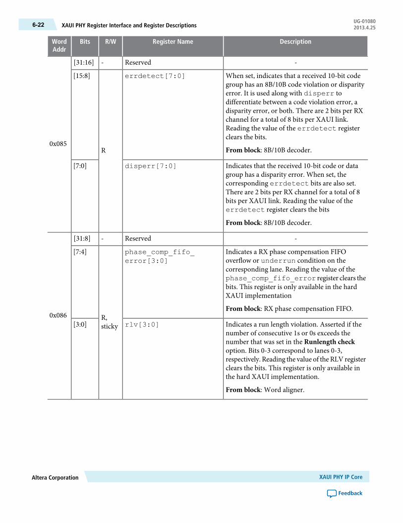
DescriptionRegister NameR/WBitsWordAddr
-Reserved-[31:16]
0x085
When set, indicates that a received 10-bit codegroup has an 8B/10B code violation or disparityerror. It is used along with disperr todifferentiate between a code violation error, adisparity error, or both. There are 2 bits per RXchannel for a total of 8 bits per XAUI link.Reading the value of the errdetect registerclears the bits.
From block: 8B/10B decoder.
errdetect[7:0]
R
[15:8]
Indicates that the received 10-bit code or datagroup has a disparity error. When set, thecorresponding errdetect bits are also set.There are 2 bits per RX channel for a total of 8bits per XAUI link. Reading the value of theerrdetect register clears the bits
From block: 8B/10B decoder.
disperr[7:0][7:0]
-Reserved-[31:8]
0x086
Indicates a RX phase compensation FIFOoverflow or underrun condition on thecorresponding lane. Reading the value of thephase_comp_fifo_error register clears thebits. This register is only available in the hardXAUI implementation
From block: RX phase compensation FIFO.
phase_comp_fifo_error[3:0]
R,sticky
[7:4]
Indicates a run length violation. Asserted if thenumber of consecutive 1s or 0s exceeds thenumber that was set in the Runlength checkoption. Bits 0-3 correspond to lanes 0-3,respectively. Reading the value of the RLV registerclears the bits. This register is only available inthe hard XAUI implementation.
From block: Word aligner.
rlv[3:0][3:0]
XAUI PHY IP CoreAltera Corporation
Feedback
UG-01080XAUI PHY Register Interface and Register Descriptions6-22 2013.4.25

DescriptionRegister NameR/WBitsWordAddr
-Reserved-[31:16]
0x087
When asserted, indicates that the RX rate matchblock inserted a ||R|| column. Goes high for oneclock cycle per inserted ||R|| column. Reading thevalue of the rmfifodatainserted registerclears the bits. This register is only available inthe hard XAUI implementation.
From block: Rate match FIFO.
rmfifodatainserted[7:0]
R,sticky
[15:8]
When asserted, indicates that the ratematch blockhas deleted an ||R|| column. The flag goes highfor one clock cycle per deleted ||R|| column. Thereare 2 bits for each lane. Reading the value of thermfifodatadeleted register clears the bits.This register is only available in the hard XAUIimplementation.
From block: Rate match FIFO.
rmfifodatadeleted[7:0][7:0]
-Reserved-[31:8]
0x088
When asserted, indicates that rate match FIFO isfull (20 words). Bits 0-3 correspond to lanes 0-3,respectively. Reading the value of thermfifofull register clears the bits. Thisregister is only available in the hard XAUIimplementation
From block: Rate match FIFO.
rmfifofull[3:0]
R,sticky
[7:4]
When asserted, indicates that the ratematch FIFOis empty (5 words). Bits 0-3 correspond to lanes0-3, respectively. Reading the value of thermfifoempty register clears the bits. Thisregister is only available in the hard XAUIimplementation
From block: Rate match FIFO.
rmfifoempty[3:0][3:0]
Altera CorporationXAUI PHY IP Core
Feedback
6-23XAUI PHY Register Interface and Register DescriptionsUG-010802013.4.25

DescriptionRegister NameR/WBitsWordAddr
-Reserved-[31:3]
0x089
Indicates a TX phase compensation FIFOoverflow or underrun condition on thecorresponding lane. Reading the value of thephase_comp_fifo_error register clears thebits. This register is only available in the hardXAUI implementation
From block: TX phase compensation FIFO.
phase_comp_fifo_error[2:0]
R,sticky
[2:0]
Setting this bit to 1 shortens the duration of resetand loss timer when simulating. Alterarecommends that you keep this bit set duringsimulation.
simulation_flagRW[0]0x08a
For more information about the individual PCS blocks, refer to the Transceiver Architecture chapters of theappropriate device handbook.
Related InformationAvalon Interface Specifications
Transceiver Architecture in Arria II Devices
Transceiver Architecture in Arria V Devices
Cyclone IV Transceivers Architecture
Transceiver Architecture in Cyclone V Devices
Transceiver Architecture in HardCopy IV Devices
Transceiver Architecture in Stratix IV Devices
Transceiver Architecture in Stratix V Devices
Loopback Modes on page 16-50
XAUI PHY Dynamic Reconfiguration for Arria II GX, Cyclone IV GX, HardCopyIV GX, and Stratix IV GX
The Arria II GX, Cyclone IV GX, HardCopy IV GX, and Stratix IV GX use the ALTGX_RECONFIG Megafunction for transceiver reconfiguration.
For more information about the ALTGX_RECONFIG Megafunction, refer to ALTGX_RECONFIGMegafunction User Guide for Stratix IV Devices in volume 2 of the Stratix IV Device Handbook.
If your XAUI PHY IP Core includes a single transceiver quad, these signals are internal to the core. If yourdesign uses more than one quad, the reconfiguration signals are external.
XAUI PHY IP CoreAltera Corporation
Feedback
UG-01080XAUI PHY Dynamic Reconfiguration for Arria II GX, Cyclone IV GX, HardCopy IV GX, and Stratix IV GX6-24 2013.4.25

Table 6-16: Dynamic Reconfiguration Interface Arria II GX, Cyclone IV GX, HardCopy IV GX, and Stratix IVGX devices
DescriptionDirectionSignal Name
Reconfiguration signals from theTransceiver ReconfigurationIP Core to the XAUI transceiver.
Inputreconfig_to_xcvr[3:0]
Reconfiguration signals from the XAUI transceiver to theTransceiver Reconfiguration IP Core. The size of this bus isdepends on the device. For the soft PCS in Stratix IV GX andGT devices, <n> = 68 bits. For hard XAUI variants, <n> =16. For Stratix V devices, the number of bits depends on thenumber of channels specified. Refer to Chapter 16,Transceiver Reconfiguration Controller IP Core for moreinformation.
Outputreconfig_from_xcvr[<n>:0]
Related InformationALTGX_RECONFIG Megafunction User Guide for Stratix IV Devices
Transceiver Reconfiguration Controller IP Core Overview on page 16-1
XAUI PHY Dynamic Reconfiguration for Arria V, Cyclone V and Stratix VDevices
The Arria V, Cyclone V, and Stratix V devices use the Transceiver Reconfiguration Controller IP Core fordynamic reconfiguration.
For more information about this IP core, refer to Chapter 16, Transceiver Reconfiguration Controller IPCore.
Each channel and each TX PLL have separate dynamic reconfiguration interfaces. The MegaWizard Plug-InManager provides informational messages on the connectivity of these interfaces.
Example 6-2: Informational Messages for the Transceiver Reconfiguration Interface
PHY IP will require 8 reconfiguration interfaces for connectionto the external reconfiguration controller.Reconfigurationinterface offsets 0-3 are connected to the transceiverchannels.Reconfiguration interface offsets 4-7 are connected tothe transmit PLLs.
Although you must initially create a separate reconfiguration interface for each channel and TX PLL in yourdesign, when theQuartus II software compiles your design, it reduces the number of reconfiguration interfacesby merging reconfiguration interfaces. The synthesized design typically includes a reconfiguration interfacefor at least three channels because three channels share an Avalon-MM slave interface which connects tothe Transceiver Reconfiguration Controller IP Core. Conversely, you cannot connect the three channelsthat share an Avalon-MM interface to different Transceiver Reconfiguration Controller IP Cores. Doing socauses a Fitter error. For more information, refer to “Transceiver Reconfiguration Controller to PHY IPConnectivity”.
Altera CorporationXAUI PHY IP Core
Feedback
6-25XAUI PHY Dynamic Reconfiguration for Arria V, Cyclone V and Stratix V DevicesUG-010802013.4.25
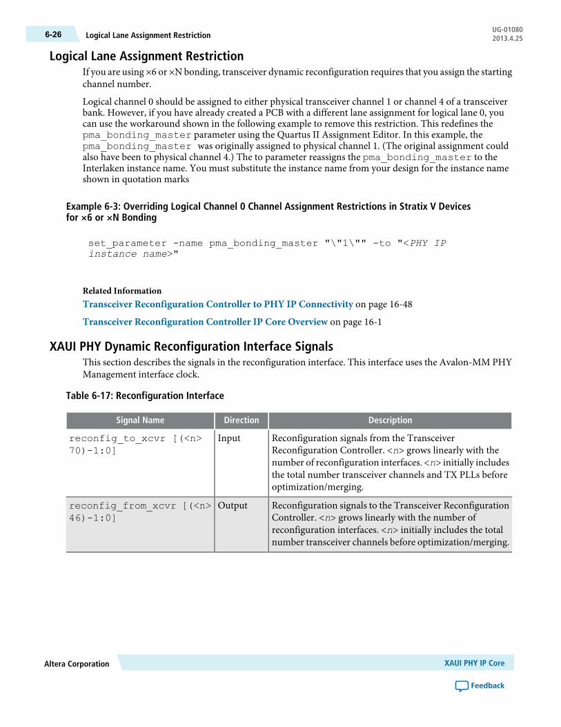
Logical Lane Assignment RestrictionIf you are using ×6 or ×N bonding, transceiver dynamic reconfiguration requires that you assign the startingchannel number.
Logical channel 0 should be assigned to either physical transceiver channel 1 or channel 4 of a transceiverbank. However, if you have already created a PCB with a different lane assignment for logical lane 0, youcan use the workaround shown in the following example to remove this restriction. This redefines thepma_bonding_master parameter using the Quartus II Assignment Editor. In this example, thepma_bonding_master was originally assigned to physical channel 1. (The original assignment couldalso have been to physical channel 4.) The to parameter reassigns the pma_bonding_master to theInterlaken instance name. You must substitute the instance name from your design for the instance nameshown in quotation marks
Example 6-3: Overriding Logical Channel 0 Channel Assignment Restrictions in Stratix V Devicesfor ×6 or ×N Bonding
set_parameter -name pma_bonding_master "\"1\"" -to "<PHY IPinstance name>"
Related InformationTransceiver Reconfiguration Controller to PHY IP Connectivity on page 16-48
Transceiver Reconfiguration Controller IP Core Overview on page 16-1
XAUI PHY Dynamic Reconfiguration Interface SignalsThis section describes the signals in the reconfiguration interface. This interface uses the Avalon-MM PHYManagement interface clock.
Table 6-17: Reconfiguration Interface
DescriptionDirectionSignal Name
Reconfiguration signals from the TransceiverReconfiguration Controller. <n> grows linearly with thenumber of reconfiguration interfaces. <n> initially includesthe total number transceiver channels and TX PLLs beforeoptimization/merging.
Inputreconfig_to_xcvr [(<n>70)-1:0]
Reconfiguration signals to the Transceiver ReconfigurationController. <n> grows linearly with the number ofreconfiguration interfaces. <n> initially includes the totalnumber transceiver channels before optimization/merging.
Outputreconfig_from_xcvr [(<n>46)-1:0]
XAUI PHY IP CoreAltera Corporation
Feedback
UG-01080Logical Lane Assignment Restriction6-26 2013.4.25

Related InformationTransceiver Reconfiguration Controller to PHY IP Connectivity on page 16-48
Transceiver Reconfiguration Controller IP Core Overview on page 16-1
Simulation Files and Example TestbenchRefer to “Running a Simulation Testbench” for a description of the directories and files that the Quartus IIsoftware creates automatically when you generate your XAUI PHY IP Core.
Refer to the Altera Wiki for an example testbench that you can use as a starting point in creating your ownverification environment.
Related InformationAltera Wiki
Running a Simulation Testbench on page 1-6
Altera CorporationXAUI PHY IP Core
Feedback
6-27Simulation Files and Example TestbenchUG-010802013.4.25

7Interlaken PHY IP Core
2013.4.25UG-01080 Subscribe Feedback
The Altera Interlaken PHY IP Core implements Interlaken Protocol Specification, Rev 1.2.
Interlaken is a high speed serial communication protocol for chip-to-chip packet transfers. It supportsmultiple instances, each with 1 to 24 lanes running at 10.3125 Gbps or greater in Arria V GZ and Stratix Vdevices. The key advantages of Interlaken are scalability and its low I/O count compared to earlier protocolssuch as SPI 4.2. Other key features include flow control, low overhead framing, and extensive integritychecking. The Interlaken physical coding sublayer (PCS) transmits and receivesAvalon-STdata on its FPGAfabric interface. It transmits and receives high speed differential serial data using the PCML I/O standard.
Figure 7-1: Interlaken PHY IP Core
PCS PMA
SerializerFraming:
GearboxBlock Synchronization
64b/67b Encoding/DecodingScrambing/Descrambling
Lane-Based CRC32DC Balancing
De-Serializerand CDR
HSSI I/O
Interlaken PHY IP Core
FPGAFabric
tx_serial_dataAvalon-STTx and Rx
rx_serial_data
up to10.3125 Gbps
Formore information about theAvalon-ST protocol, including timing diagrams, refer to theAvalon InterfaceSpecifications.
Interlaken operates on 64-bit data words and 3 control bits, which are striped round robin across the lanesto reduce latency. Striping renders the interface independent of exact lane count. The protocol acceptspackets on 256 logical channels and is expandable to accommodate up to 65,536 logical channels. Packetsare split into small bursts which can optionally be interleaved. The burst semantics include integrity checkingand per channel flow control.
ISO9001:2008Registered
© 2013 Altera Corporation. All rights reserved. ALTERA, ARRIA, CYCLONE, HARDCOPY, MAX, MEGACORE, NIOS, QUARTUS and STRATIXwords and logos are trademarks of Altera Corporation and registered in the U.S. Patent and Trademark Office and in other countries. All other wordsand logos identified as trademarks or service marks are the property of their respective holders as described at www.altera.com/common/legal.html.Altera warrants performance of its semiconductor products to current specifications in accordance with Altera's standard warranty, but reserves theright to make changes to any products and services at any time without notice. Altera assumes no responsibility or liability arising out of the applicationor use of any information, product, or service described herein except as expressly agreed to in writing by Altera. Altera customers are advised toobtain the latest version of device specifications before relying on any published information and before placing orders for products or services.
www.altera.com
101 Innovation Drive, San Jose, CA 95134
The Interlaken PCS supports the following framing functions on a per lane basis:
• Gearbox• Block synchronization• Metaframe generation and synchronizatio• 64b/67b encoding and decoding• Scrambling and descrambling• Lane-based CRC32• Disparity DC balancing
For more detailed information about the Interlaken transceiver channel datapath, clocking, and channelplacement in Stratix V devices, refer to the “Interlaken” section in the Transceiver Configurations in StratixV Devices chapter of the Stratix V Device Handbook.
For more detailed information about the Interlaken transceiver channel datapath, clocking, and channelplacement in Arria V GZ devices, refer to the “Interlaken” section in the Transceiver Configurations in ArriaV Devices chapter of the Arria V Device Handbook.
Refer to PHY IP Design Flow with Interlaken for Stratix V Devices for a reference design that implementsthe Interlaken protocol in a Stratix V device.
Related InformationInterlaken Protocol Specification, Rev 1.2
Avalon Interface Specifications
Transceiver Configurations in Stratix V Devices
Transceiver Configurations in Arria V Devices
PHY IP Design Flow with Interlaken for Stratix V Devices
Interlaken PHY Device Family SupportThis section describes the Interlaken PHY device family support.
IP cores provide either final or preliminary support for target Altera device families. These terms have thefollowing definitions:
• Final support—Verified with final timing models for this device.• Preliminary support—Verified with preliminary timing models for this device.
Table 7-1: Device Family Support
SupportDevice Family
PreliminaryArria V GZ devices–Hard PCS + PMA
PreliminaryStratix V devices–Hard PCS + PMA
Not supportedOther device families
Interlaken PHY IP CoreAltera Corporation
Feedback
UG-01080Interlaken PHY Device Family Support7-2 2013.4.25
Parameterizing the Interlaken PHYThe Interlaken PHY IP Core is available when you select the Arria V GZ or Stratix V devices. Completethe following steps to configure the Interlaken PHY IP Core in the MegaWizard Plug-In Manager:
1. For Which device family will you be using?, select Arria V GZ or Stratix V.2. Click Installed Plug-Ins > Interfaces > Interlaken > Interlaken PHY v12.1.3. Use the tabs on the MegaWizard Plug-In Manager to select the options required for the protocol.4. Refer to the following topics to learn more about the parameters:
a. General Parametersb. Optional Port Parametersc. Analog Options
5. Click Finish to generate your parameterized Interlaken PHY IP Core.
Interlaken PHY General ParametersThis section describes the Interlaken PHY parameters you can set on the General tab.
Table 7-2: Interlaken PHY General Options
DescriptionValueParameter
Specifies the device family.Arria V GZ
Stratix V
Device family
Specifies the mode of operation as Duplex, RX,or TX mode.
Duplex,
RX,
TX
Datapath mode
Specifies the lane data rate. The Input clockfrequency and Base data rate parameters updateautomatically based on the Lane rate you specify.
Custom, user-defined, lane data rates are nowsupported. However, the you must choose a lanedata rate that results in a standard board oscillatorreference clock frequency to drive thepll_ref_clk and meet jitter requirements. Choosing alane data rate that deviates from standardreference clock frequencies may result in customboard oscillator clock frequencies which may beprohibitively expensive or unavailable.
3125 Mbps
5000 Mbps
6250 Mbps
6375 Mbps
10312.5 Mbps
10312.5 Mbps
12500 Mbps
Custom
Lane rate
Specifies the number of lanes in a link over whichdata is striped.
1-24Number of lanes
Altera CorporationInterlaken PHY IP Core
Feedback
7-3Parameterizing the Interlaken PHYUG-010802013.4.25
DescriptionValueParameter
Specifies the number of words in a metaframe.The default value is 2048.
Although 5 -8191 words are valid metaframelength values, the current Interlaken PHY IPCoreimplementation requires a minimum of 128Metaframe length for good, stable performance.
In simulation, Altera recommends that you use asmaller metaframe length to reduce simulationtimes.
5-8191Metaframe length inwords
Specifies the frequency of the input referenceclock. The default value for the Input clockfrequency is the Lane rate /20. Many referenceclock frequencies are available.
Lane rate/<n>
Lane rate/80
Lane rate/64
Lane rate/50
Lane rate/40
Lane rate/32
Lane rate/25
Lane rate/20
Lane rate/16
Lane rate/12.5
Lane rate/10
Lane rate/8
Input clock frequency
Specifies the PLL type.
The CMU PLL has a larger frequency range thanthe ATX PLL. The ATX PLL is designed toimprove jitter performance and achieves lowerchannel-to-channel skew; however, it supports anarrower range of lane data rates and referenceclock frequencies. Another advantage of the ATXPLL is that it does not use a transceiver channel,while the CMU PLL does. Because the CMU PLLis more versatile, it is specified as the defaultsetting.
CMU
ATX
PLL type
Interlaken PHY IP CoreAltera Corporation
Feedback
UG-01080Interlaken PHY General Parameters7-4 2013.4.25

DescriptionValueParameter
This option allows you to specify aBase data rateto minimize the number of PLLs required togenerate the clocks necessary for data transmissionat different frequencies. Depending on the Lanerate you specify, the default Base data rate can beeither 1, 2, or 4 times the Lane rate; however, youcan change this value. The default value specifiedis for backwards compatibilitywith earlierQuartusII software releases.
1 × Lane rate
2 × Lane rate
3 × Lane rate
Base data rate
Interlaken PHY Optional Port ParametersThis section describes the Interlaken PHY optional port parameters you can set on the Optional Ports tab.
Table 7-3: Optional Ports
DescriptionValueParameter
When you turn this option on, rx_parallel_data[71:69] are included in the top-levelmodule. These optional signals report the statusof word and synchronization locks and CRC32errors. Refer to Avalon-ST RX Signals for moreinformation.
On/OffEnable RX status signals,(word lock, sync lock,crc32 error) as part ofrx_parallel_data
The tx_coreclkin drives the write side of TXFIFO. This clock is required for multi-lanesynchronization but is optional for single laneInterlaken links.
If tx_coreclkin is deselected for single laneInterlaken links, tx_user_clkout drives theTX side of the write FIFO. You must use the tx_user_clkout output port to drive transmitdata in the Interlaken MAC.
On/OffCreate tx_coreclkin port
When selected rx_coreclkin is available asinput port which drives the read side of RX FIFO,When deselected rx_user_clkout, rx_clkout for all bonded receiver lanes, is routedinternally to drive the RX read side of FIFO. rx_user_clkout is also available as an output portfor the Interlaken MAC.
On/OffCreate rx_coreclkin port
Interlaken PHY Analog ParametersThis section describes the Interlaken PHY analog parameters.
Altera CorporationInterlaken PHY IP Core
Feedback
7-5Interlaken PHY Optional Port ParametersUG-010802013.4.25
Click on the appropriate link to specify the analog options for your device:
Related InformationAnalog Settings for Arria V GZ Devices on page 19-9
Analog Settings for Stratix V Devices on page 19-25
Interlaken PHY InterfacesThis section describes the Interlaken PHY interfaces.
The following figure illustrates the top-level signals of the Interlaken PHY IPCore; <n> is the channel numberso that the width of tx_data in 4-lane instantiation is [263:0].
Figure 7-2: Top-Level Interlaken PHY Signals
tx_parallel_data<n> [65:0]tx_readytx_datain_bp<n>tx_clkout<n>tx_user_clkoutpll_lockedtx_sync_done
rx_parallel_data<n> [71:0]rx_readyrx_clkout<n>rx_fifo_clr<n>rx_dataout_bp<n>
phy_mgmt_clkphy_mgmt_clk_resetphy_mgmt_address[8:0]phy_mgmt_writedata[31:0]phy_mgmt_readdata[31:0]phy_mgmt_writephy_mgmt_readphy_mgmt_waitrequest
pll_ref_clk
Interlaken Top-Level Signals
tx_serial_data<n>rx_serial_data<n>
Avalon-STTX to/ from
MAC
High SpeedSerial I/O
PLL
Avalon-MM PHYManagementInterface
Avalon-STRX from/to
MAC DynamicReconfiguation
tx_coreclkinrx_coreclkin
reconfig_to_xcvr[(<n> 70-1):0]reconfig_from_xcvr[(<n> 46-1):0]
FIFO ClockInput
(Optional)
The block diagram shown in the GUI labels the external pins with the interface type and places theinterface name inside the box. The interface type and name are used to define interfaces in the _hw.tcl.writing.
Note:
For more information about _hw.tcl, files refer to the Component Interface Tcl Reference chapter in volume1 of the Quartus II Handbook.
Related InformationComponent Interface Tcl Reference
Interlaken PHY Avalon-ST TX InterfaceThis section lists the signals in the Avalon-ST TX interface.
Interlaken PHY IP CoreAltera Corporation
Feedback
UG-01080Interlaken PHY Interfaces7-6 2013.4.25

Table 7-4: Avalon-ST TX Signals
DescriptionDirectionSignal Name
Avalon-ST data bus driven from the FPGA fabric to theTX PCS. This input should be synchronized to the tx_coreclkin clock domain.
Inputtx_parallel_data<n>[63:0]
Indicates whether tx_parallel_data<n>[63:0]represents control or data. When deasserted, tx_parallel_data<n>[63:0] is a data word. Whenasserted,tx_parallel_data<n>[63:0] is a controlword.
The value of header synchronization bits[65:64] of theInterlakenword identify whether bits[63:0] are a FramingLayer Control/Burst/IDLEControlWord or a data word.The MAC must gray encode the header synchronizationbits. The value 2'b10 indicatingBurst/IDLEControlWordmust be gray encoded to the value 1'b1 for tx_parallel_data<n>[64]. The value 2'b01 indicatingdata wordmust be gray encoded to the value 1'b0 fortx_parallel_data<n>[64]. You can also tie headersynchronization bit[65] totx_parallel_data[64]directly.
Inputtx_parallel_data<n>[64]
Whenasserted, indicates thattx_parallel_data<n>[63:0] is valid and is ready to be written into the TXFIFO.When deasserted, indicates thattx_parallel_data<n>[63:0] is invalid and is not written into theTX FIFO. This signal is the data valid or write enable portof the TX FIFO. This input must be synchronized to thetx_coreclkin clock domain.
The Interlaken MAC should gate tx_parallel_data<n>[65] based on tx_datain_bp<n>. Or,you can tie tx_datain_bp<n> directly to tx_parallel_data<n>[65]. For Quartus II releasesbefore 12.0, you must pre-fill the transmit FIFO so thispinmust be 1'b1whentx_ready is asserted, but beforetx_sync_done is asserted to insert the pre-fill pattern.Do not use valid data to pre-fill the transmit FIFO. Usethe following Verilog HDL assignment for Quartus IIreleases prior to 12.0:
assign tx_parallel_data[65] = (!tx_sync_done)?1'b1:tx_datain_bp[0];
Inputtx_parallel_data<n>[65]
Altera CorporationInterlaken PHY IP Core
Feedback
7-7Interlaken PHY Avalon-ST TX InterfaceUG-010802013.4.25

DescriptionDirectionSignal Name
When asserted, indicates that the TX interface has exitedthe reset state and is ready for service. The tx_readylatency for the TX interface is 0. A 0 latency means thatthe TX FIFO can accept data on the same clock cycle thattx_ready is asserted. This output is synchronous tothephy_mgmt_clk clockdomain. The InterlakenMACmust wait for tx_ready before initiating data transfer(pre-fill pattern or valid user data) on any lanes. The TXFIFO only captures input data from the Interlaken MACwhentx_ready andtx_parallel_data[65] areboth asserted. The beginning of the pre-fill stage ismarked by the assertion of tx_ready, before tx_sync_done is asserted. The pre-fill stage shouldterminatewhentx_ready is high andtx_sync_donechanges from Logic 0 to Logic 1 state. At this point, TXsynchronization is complete and valid TX data insertioncan begin. TX synchronization is not required forsingle-lane variants. Use the following Verilog HDLassignment is for Quartus versions earlier than 12.0:
assign tx_parallel_data[65] = (!tx_sync_done)?1'b1:tx_datain_bp[0];
Outputtx_ready
Interlaken PHY IP CoreAltera Corporation
Feedback
UG-01080Interlaken PHY Avalon-ST TX Interface7-8 2013.4.25

DescriptionDirectionSignal Name
When asserted, indicates that Interlaken TX lane <n>interface is ready to receive data for transmission. Inmulti-lane configurations, the tx_datain_bp<n>signals must be logically Ored. The latency on thisAvalon-ST interface is 0 cycles. The InterlakenMACmustonly drive valid user data ontx_parallel_data<n>[64] and tx_parallel_data<n>[63:0] databus as soon as tx_ready<n> and tx_sync_doneare both asserted. The tx_datain_bp<n> signal isconnected to the partial empty threshold of the TXFIFO,so that when tx_datain_bp<n> is deasserted the TXFIFO back pressures the Interlaken MAC. Stop sendingTX data to the PHY when this signal is deasserted.
The InterlakenMACcan continue driving data to the TXFIFO when tx_datain_bp<n> is asserted. TheInterlakenMACshould gatetx_parallel_data<n>[65], which operates as a data_valid signal, based ontx_datain_bp<n> . This output is synchronous tothe tx_coreclkin clock domain. Or, you can alsotie tx_datain_bp<n> directly to tx_parallel_data<n>[65] . For Quartus II releases prior to 12.0,you must pre-fill the TX FIFO before tx_sync_donecan be asserted. Do not use valid data to pre-fill the TXFIFO. Use the following Verilog HDL assignment forQuartus II releases prior to 12.0:
assign tx_parallel_data[65] = (!tx_sync_done)?1'b1:tx_datain_bp[0];
Outputtx_datain_bp<n>
For single lane Interlaken links, tx_user_clkout isavailable when you do not create the optional tx_coreclkin . For Interlaken linkswithmore than 1 lane,tx_coreclkin is required and tx_user_clkoutcannot be used.tx_coreclkinmust have aminimumfrequency of the lane data rate divided by 67. Thefrequency range for tx_coreclkin is (data rate/40)- (data rate/67). For best results, Altera recommends thattx_coreclkin = (data rate/40).
Outputtx_clkout
For single lane Interlaken links, tx_user_clkout isavailable when you do not create the optional tx_coreclkin. For Interlaken linkswithmore than 1 lane,tx_coreclkin is required and tx_user_clkoutcannot be used.tx_coreclkinmust have aminimumfrequency of the lane data rate divided by 40.
Outputtx_user_clkout
Altera CorporationInterlaken PHY IP Core
Feedback
7-9Interlaken PHY Avalon-ST TX InterfaceUG-010802013.4.25

DescriptionDirectionSignal Name
In multilane Interlaken designs, this signal is the bitwiseAND of the individual lane pll_locked signals. Thisoutput is synchronous to the phy_mgmt_clk clockdomain.
Outputpll_locked
When asserted, indicates that alltx_parallel_datalanes are synchronized and ready for valid user datatraffic. The Interlaken MAC must wait for this signal tobe asserted before initiating valid user data transfers onany lane. This output is synchronous to the tx_coreclkin clock domain. For consistent tx_sync_done performance, Altera recommends using tx_coreclkin and rx_coreclkin frequency of lane(data rate/40).
Youmust invoke a hard reset usingmgmt_rst_resetand phy_mgmt_clk_reset to initiate thesynchronization sequence on the TX lanes.
After tx_sync_done is asserted, youmust never allowthe TX FIFO to underflow, doing so requires you to hardreset to the Interlaken PHY IP Core.
For Quartus versions prior to 12.0, you must pre-fill theTX FIFO before tx_sync_done can be asserted. Usethe following Verilog HDL assignment for Quartus IIreleases prior to 12.0:
assign tx_parallel_data[65] = (!tx_sync_done)?1'b1:tx_datain_bp[0];
Outputtx_sync_done
Interlaken PHY Avalon-ST RX InterfaceThis section lists the signals in the Avalon-ST RX interface.
Table 7-5: Avalon-ST RX Signals
DescriptionDirectionSignal Name
Avalon-ST data bus driven from the RX PCS to the FPGA fabric.This output is synchronous to the rx_coreclkin clock domain.
Outputrx_parallel_data<n>[63:0]
Interlaken PHY IP CoreAltera Corporation
Feedback
UG-01080Interlaken PHY Avalon-ST RX Interface7-10 2013.4.25
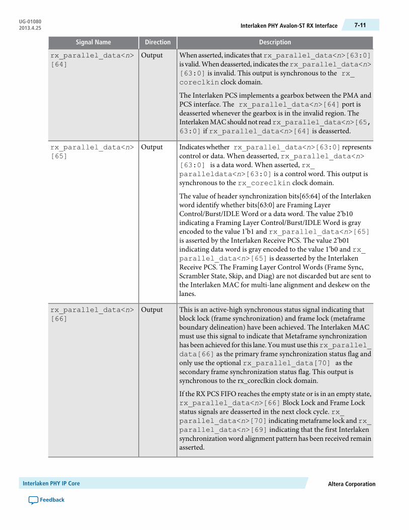
DescriptionDirectionSignal Name
Whenasserted, indicates thatrx_parallel_data<n>[63:0]is valid.Whendeasserted, indicates therx_parallel_data<n>[63:0] is invalid. This output is synchronous to the rx_coreclkin clock domain.
The Interlaken PCS implements a gearbox between the PMA andPCS interface. The rx_parallel_data<n>[64] port isdeasserted whenever the gearbox is in the invalid region. TheInterlakenMACshouldnot readrx_parallel_data<n>[65,63:0] if rx_parallel_data<n>[64] is deasserted.
Outputrx_parallel_data<n>[64]
Indicateswhether rx_parallel_data<n>[63:0] representscontrol or data. When deasserted, rx_parallel_data<n>[63:0] is a data word. When asserted, rx_paralleldata<n>[63:0] is a control word. This output issynchronous to the rx_coreclkin clock domain.
The value of header synchronization bits[65:64] of the Interlakenword identify whether bits[63:0] are Framing LayerControl/Burst/IDLE Word or a data word. The value 2’b10indicating a Framing Layer Control/Burst/IDLE Word is grayencoded to the value 1’b1 and rx_parallel_data<n>[65]is asserted by the Interlaken Receive PCS. The value 2’b01indicating data word is gray encoded to the value 1’b0 and rx_parallel_data<n>[65] is deasserted by the InterlakenReceive PCS. The Framing Layer Control Words (Frame Sync,Scrambler State, Skip, and Diag) are not discarded but are sent tothe Interlaken MAC for multi-lane alignment and deskew on thelanes.
Outputrx_parallel_data<n>[65]
This is an active-high synchronous status signal indicating thatblock lock (frame synchronization) and frame lock (metaframeboundary delineation) have been achieved. The Interlaken MACmust use this signal to indicate that Metaframe synchronizationhas been achieved for this lane. Youmust use thisrx_parallel_data[66] as the primary frame synchronization status flag andonly use the optional rx_parallel_data[70] as thesecondary frame synchronization status flag. This output issynchronous to the rx_coreclkin clock domain.
If the RX PCS FIFO reaches the empty state or is in an empty state,rx_parallel_data<n>[66] Block Lock and Frame Lockstatus signals are deasserted in the next clock cycle. rx_parallel_data<n>[70] indicatingmetaframe lock andrx_parallel_data<n>[69] indicating that the first Interlakensynchronizationword alignment pattern has been received remainasserted.
Outputrx_parallel_data<n>[66]
Altera CorporationInterlaken PHY IP Core
Feedback
7-11Interlaken PHY Avalon-ST RX InterfaceUG-010802013.4.25

DescriptionDirectionSignal Name
When asserted, indicates an RX FIFO overflow error.Outputrx_parallel_data<n>[67]
When asserted, indicates that the RX FIFO is partially empty andis still accepting data from the frame synchronizer. This signal isasserted when the RX FIFO fill level is below the rx_fifo_pempty threshold. This output is synchronous to the rx_coreclkin clock domain. To prevent underflow, the InterlakenMAC should begin reading from the RX FIFO when this signal isdeasserted, indicating sufficient FIFO contents (RX FIFO levelaboverx_fifo_pempty threshold). TheMAC should continueto read the RX FIFO to prevent overflow as long as this signal isnot reasserted. You can assert a FIFO flush using the rx_fifo_clr<n> when the receive FIFO overflows. This output issynchronous to the rx_clkout clock domain. Therefore, youmust synchronize rx_parallel_data<n>[68] to the rx_coreclkin before making the assignment below.
You can tie this signal's inverted logic to the rx_dataout_bp<n> receive FIFO read enable signal as the followingassignment statement illustrates:
assign rx_dataout_bp[0] =!(rx_parallel_data[68]);
Outputrx_parallel_data<n>[68]
When asserted, indicates that the RX FIFO has found the firstInterlaken synchronizationword alignment pattern. For very shortmetaframes, this signalmay be asserted after the frame synchronizerstate machine validates frame synchronization and asserts rx_parallel_data<n>[70]because this signal is asserted by theRX FIFO which is the last PCS block in the RX datapath. Thisoutput is synchronous to the rx_coreclkin clock domain.
This signal is optional. If the RX PCS FIFO reaches the empty stateor is in an empty state,rx_parallel_data<n>[70] indicatingmetaframe lock andrx_parallel_data<n>[69] indicatingthat the first Interlaken synchronization word alignment patternhas been received remain asserted, butrx_parallel_data<n>[66] block lock and frame lock status signal are deasserted in thenext clock cycle.
Outputrx_parallel_data<n>[69]
Interlaken PHY IP CoreAltera Corporation
Feedback
UG-01080Interlaken PHY Avalon-ST RX Interface7-12 2013.4.25
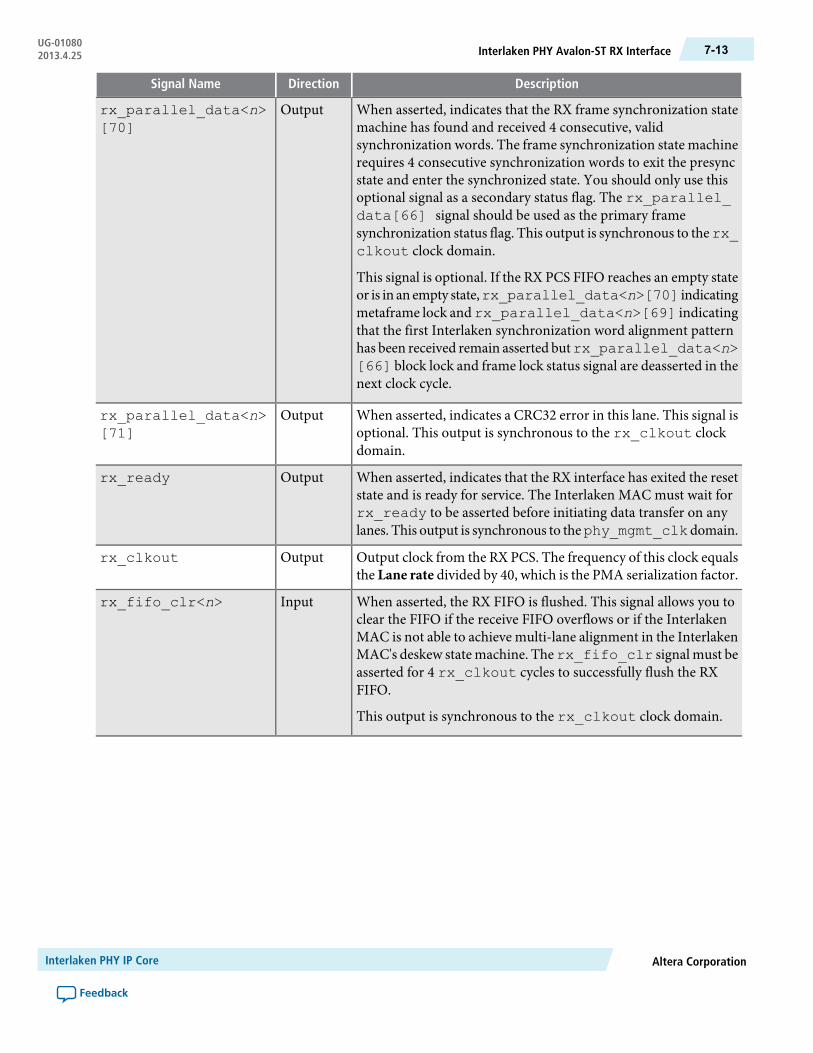
DescriptionDirectionSignal Name
When asserted, indicates that the RX frame synchronization statemachine has found and received 4 consecutive, validsynchronization words. The frame synchronization state machinerequires 4 consecutive synchronization words to exit the presyncstate and enter the synchronized state. You should only use thisoptional signal as a secondary status flag. The rx_parallel_data[66] signal should be used as the primary framesynchronization status flag. This output is synchronous to therx_clkout clock domain.
This signal is optional. If the RX PCS FIFO reaches an empty stateor is in an empty state,rx_parallel_data<n>[70] indicatingmetaframe lock andrx_parallel_data<n>[69] indicatingthat the first Interlaken synchronization word alignment patternhas been received remain asserted butrx_parallel_data<n>[66] block lock and frame lock status signal are deasserted in thenext clock cycle.
Outputrx_parallel_data<n>[70]
When asserted, indicates a CRC32 error in this lane. This signal isoptional. This output is synchronous to the rx_clkout clockdomain.
Outputrx_parallel_data<n>[71]
When asserted, indicates that the RX interface has exited the resetstate and is ready for service. The Interlaken MAC must wait forrx_ready to be asserted before initiating data transfer on anylanes. This output is synchronous to thephy_mgmt_clkdomain.
Outputrx_ready
Output clock from the RX PCS. The frequency of this clock equalsthe Lane rate divided by 40, which is the PMA serialization factor.
Outputrx_clkout
When asserted, the RX FIFO is flushed. This signal allows you toclear the FIFO if the receive FIFO overflows or if the InterlakenMAC is not able to achieve multi-lane alignment in the InterlakenMAC's deskew state machine. Therx_fifo_clr signal must beasserted for 4 rx_clkout cycles to successfully flush the RXFIFO.
This output is synchronous to the rx_clkout clock domain.
Inputrx_fifo_clr<n>
Altera CorporationInterlaken PHY IP Core
Feedback
7-13Interlaken PHY Avalon-ST RX InterfaceUG-010802013.4.25
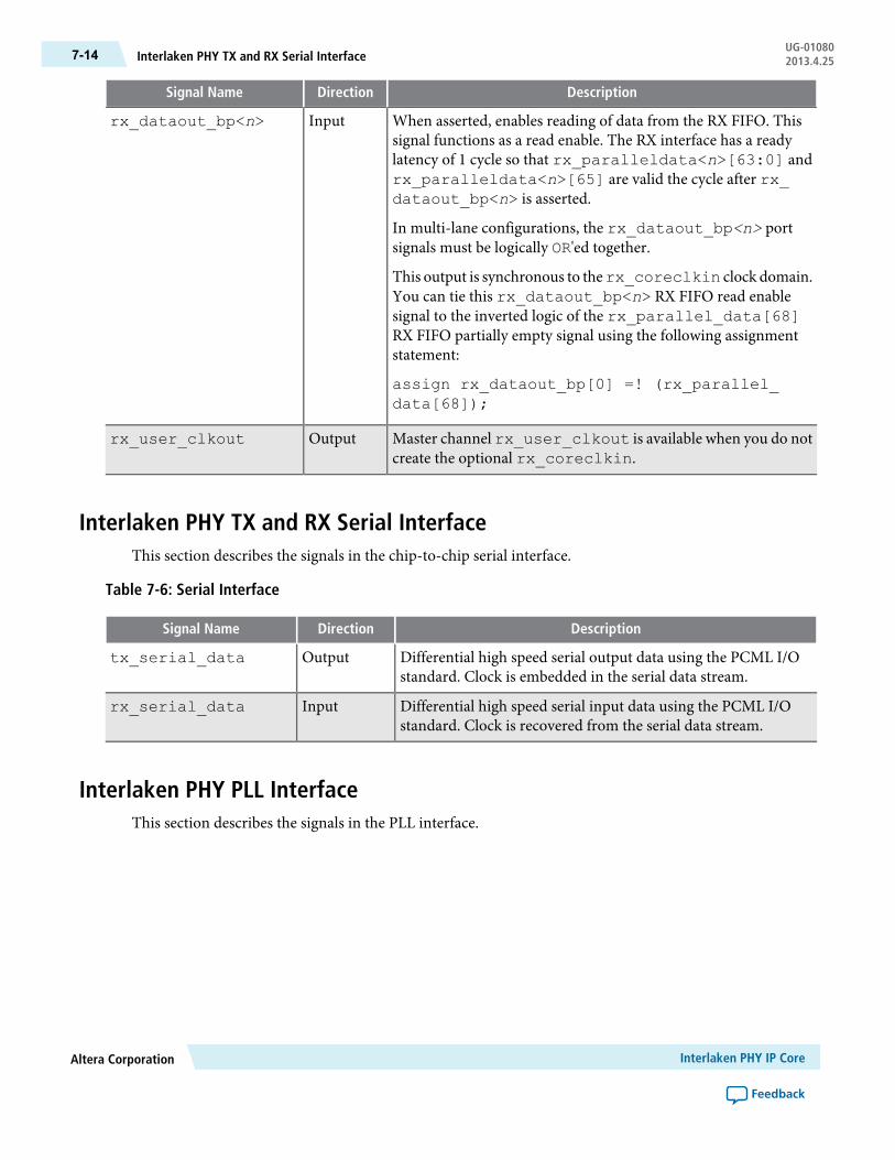
DescriptionDirectionSignal Name
When asserted, enables reading of data from the RX FIFO. Thissignal functions as a read enable. The RX interface has a readylatency of 1 cycle so that rx_paralleldata<n>[63:0] andrx_paralleldata<n>[65] are valid the cycle after rx_dataout_bp<n> is asserted.
In multi-lane configurations, the rx_dataout_bp<n> portsignals must be logically OR'ed together.
This output is synchronous to therx_coreclkin clock domain.You can tie this rx_dataout_bp<n> RX FIFO read enablesignal to the inverted logic of the rx_parallel_data[68]RX FIFO partially empty signal using the following assignmentstatement:
assign rx_dataout_bp[0] =! (rx_parallel_data[68]);
Inputrx_dataout_bp<n>
Master channel rx_user_clkout is available when you do notcreate the optional rx_coreclkin.
Outputrx_user_clkout
Interlaken PHY TX and RX Serial InterfaceThis section describes the signals in the chip-to-chip serial interface.
Table 7-6: Serial Interface
DescriptionDirectionSignal Name
Differential high speed serial output data using the PCML I/Ostandard. Clock is embedded in the serial data stream.
Outputtx_serial_data
Differential high speed serial input data using the PCML I/Ostandard. Clock is recovered from the serial data stream.
Inputrx_serial_data
Interlaken PHY PLL InterfaceThis section describes the signals in the PLL interface.
Interlaken PHY IP CoreAltera Corporation
Feedback
UG-01080Interlaken PHY TX and RX Serial Interface7-14 2013.4.25

Table 7-7: PLL Interface
DescriptionDirectionSignal Name
Reference clock for the PHY PLLs. Refer to the Lane rate entryin the Table 7-2table for required frequencies.
Custom, user-defined, data rates are now supported. However,the youmust choose a lane data rate that results in standard boardoscillator reference clock frequency to drive the pll_ref_clkand meet jitter requirements. Choosing a lane data rate thatdeviates from standard reference clock frequencies may result incustom board oscillator clock frequencies which could beunavailable or cost prohibitive.
Inputpll_ref_clk
Interlaken Optional Clocks for DeskewThis section describes the optional clocks that you can create to reduce clock skew.
Table 7-8: Deskew Clocks
DescriptionDirectionSignal Name
When enabled tx_coreclkin is available as input port whichdrives the write side of TX FIFO. Altera recommends using thisclock to reduce clock skew. The minimum frequency is datarate/67. Using a lower frequency will underflow the TX FIFOcausing the Frame Generators to go into a unrecoverable out ofalignment state and insert Skip Words into the lane. If theInterlaken TX FIFO underflows, the alignment state machinetries to recover continuously.When disabled,tx_clkoutdrivesthewrite side the TXFIFO.tx_coreclkinmust be usedwhenthe number of lanes is greater than 1.
Inputtx_coreclkin
When enabled,rx_coreclkin is available as input port whichdrives the read side of RX FIFO. Altera recommends using thisclock to reduce clock skew. You should use aminimum frequencyof lane data rate/ 67 to drive rx_coreclkin. Using a lowerfrequency overflows the RX FIFO corrupting the receiveddata.When disabled, rx_user_clkout, which is the masterrx_clkout for all the bonded receiver lanes, is internally routedto drive the read side the RX FIFO.
Inputrx_coreclkin
Interlaken PHY Register Interface and Register DescriptionsThis section describes the register interface and register descriptions.
Altera CorporationInterlaken PHY IP Core
Feedback
7-15Interlaken Optional Clocks for DeskewUG-010802013.4.25

The Avalon-MM PHY management interface provides access to the Interlaken PCS and PMA registers,resets, error handling, and serial loopback controls. You can use an embedded controller acting as anAvalon-MM master to send read and write commands to this Avalon-MM slave interface.
Table 7-9: Avalon-MM PCS Management Interface
DescriptionDirectionSignal Name
Avalon-MM clock input.
There is no frequency restriction for Stratix V devices; however,if you plan to use the same clock for the PHY managementinterface and transceiver reconfiguration, you must restrict thefrequency range of phy_mgmt_clk to 100–150 MHz to meetthe specification for the transceiver reconfiguration clock.
Inputphy_mgmt_clk
Global reset signal that resets the entire Interlaken PHY. Thissignal is active high and level sensitive.
When the Interlaken PHY IP connects to the Transceiver PHYReconfiguration Controller IP Core, the Transceiver PHYReconfigurationControllermgmt_rst_reset signalmust besimultaneously assertedwith thephy_mgmt_clk_reset signalto bring the Frame Generators in the link into alignment. This isa mandatory requirement. Failure to comply to this requirementwill result in excessive transmit lane-to-lane skew in the Interlakenlink.
Inputphy_mgmt_clk_reset
9-bit Avalon-MM address.Inputphy_mgmt_addr[8:0]
Input data.Inputphy_mgmt_writedata[31:0]
Output data.Outputphy_mgmt_readdata[31:0]
Write signal.Inputphy_mgmt_write
Read signal.Inputphy_mgmt_read
When asserted, indicates that the Avalon-MM slave interface isunable to respond to a read or write request. When asserted,control signals to the Avalon-MM slave interface must remainconstant.
Outputphy_mgmt_waitrequest
The following table specifies the registers that you can access using the Avalon-MM PHY managementinterface using word addresses and a 32-bit embedded processor. A single address space provides access toall registers. Writing to reserved or undefined register addresses may have undefined side effects.
All undefined register bits are reserved.Note:
Interlaken PHY IP CoreAltera Corporation
Feedback
UG-01080Interlaken PHY Register Interface and Register Descriptions7-16 2013.4.25

Table 7-10: Interlaken PHY Registers
DescriptionRegister NameR/WBitsWord Addr
PMA Common Control and Status Registers
If <p> is the PLL number, Bit[<p>] indicatesthat the TX CMU PLL (<p>) is locked to theinput reference clock. There is typically onepma_tx_pll_is_locked bit per system.
pma_tx_pll_is_locked
RO[<p>-1:0]0x022
Reset Control Registers-Automatic Reset Controller
Reset controller channel bitmask for digitalresets. The default value is all 1s. Channel <n>can be reset when bit<n> = 1. Channel <n>cannot be reset when bit<n> = 0.
The Interlaken PHY IP requires the use of theembedded reset controller to initiate thecorrect the reset sequence. A hard reset tophy_mgmt_clk_reset and mgmt_rst_reset is required for Interlaken PHY IP.
Altera does not recommend use of a soft resetor the use of these reset register bits forInterlaken PHY IP.
reset_ch_bitmaskRW[31:0]0x041
Writing a 1 to bit 0 initiates a TX digital resetusing the reset controller module. The resetaffects channels enabled in the reset_ch_bitmask. Writing a 1 to bit 1 initiates a RXdigital reset of channels enabled in thereset_ch_bitmask.
reset_control (write)WO
[1:0]0x042
Reading bit 0 returns the status of the resetcontroller TX ready bit. Reading bit 1 returnsthe status of the reset controller RX ready bit.
reset_status(read)RO
Reset Controls -Manual Mode
Altera CorporationInterlaken PHY IP Core
Feedback
7-17Interlaken PHY Register Interface and Register DescriptionsUG-010802013.4.25
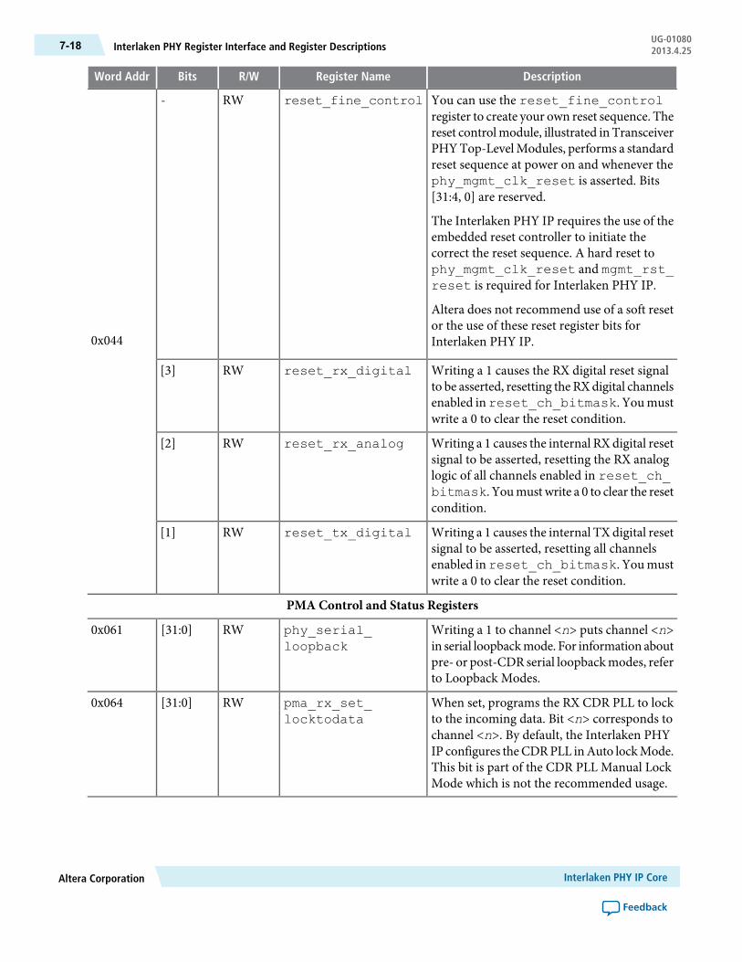
DescriptionRegister NameR/WBitsWord Addr
You can use the reset_fine_controlregister to create your own reset sequence. Thereset controlmodule, illustrated in TransceiverPHYTop-LevelModules, performs a standardreset sequence at power on and whenever thephy_mgmt_clk_reset is asserted. Bits[31:4, 0] are reserved.
The Interlaken PHY IP requires the use of theembedded reset controller to initiate thecorrect the reset sequence. A hard reset tophy_mgmt_clk_reset and mgmt_rst_reset is required for Interlaken PHY IP.
Altera does not recommend use of a soft resetor the use of these reset register bits forInterlaken PHY IP.
reset_fine_controlRW-
0x044
Writing a 1 causes the RX digital reset signalto be asserted, resetting the RXdigital channelsenabled inreset_ch_bitmask. You mustwrite a 0 to clear the reset condition.
reset_rx_digitalRW[3]
Writing a 1 causes the internal RX digital resetsignal to be asserted, resetting the RX analoglogic of all channels enabled in reset_ch_bitmask. Youmustwrite a 0 to clear the resetcondition.
reset_rx_analogRW[2]
Writing a 1 causes the internal TX digital resetsignal to be asserted, resetting all channelsenabled inreset_ch_bitmask. You mustwrite a 0 to clear the reset condition.
reset_tx_digitalRW[1]
PMA Control and Status Registers
Writing a 1 to channel <n> puts channel <n>in serial loopbackmode. For information aboutpre- or post-CDR serial loopbackmodes, referto Loopback Modes.
phy_serial_loopback
RW[31:0]0x061
When set, programs the RX CDR PLL to lockto the incoming data. Bit <n> corresponds tochannel <n>. By default, the Interlaken PHYIP configures theCDRPLL inAuto lockMode.This bit is part of the CDR PLL Manual LockMode which is not the recommended usage.
pma_rx_set_locktodata
RW[31:0]0x064
Interlaken PHY IP CoreAltera Corporation
Feedback
UG-01080Interlaken PHY Register Interface and Register Descriptions7-18 2013.4.25

DescriptionRegister NameR/WBitsWord Addr
When set, programs the RX CDR PLL to lockto the reference clock. Bit <n> corresponds tochannel <n>. By default, the Interlaken PHYIP configures theCDRPLL inAuto lockMode.This bit is part of the CDR PLL Manual LockMode which is not the recommended usage.
pma_rx_set_locktoref
RW[31:0]0x065
When asserted, indicates that the RXCDRPLLis locked to the RX data, and that the RX CDRhas changed from LTR to LTD mode. Bit <n>corresponds to channel <n>.
pma_rx_is_lockedtodata
RO[31:0]0x066
When asserted, indicates that the RXCDRPLLis locked to the reference clock. Bit <n>corresponds to channel <n>.
pma_rx_is_lockedtoref
RO[31:0]00x067
Provides for indirect addressing of all PCScontrol and status registers. Use this registerto specify the logical channel address of thePCS channel you want to access.
indirect_addrWO[31:0]0x080
Device Registers
Asserted by the CRC32 checker to indicate aCRC error in the corresponding RX lane.
From block: CRC32 checker.
rx_crc32_errRO[27]
Asserted by the frame synchronizer to indicatethat 4 frame synchronizationwords have beenreceived so that the RX lane is synchronized.
From block: Frame synchronizer.
rx_sync_lockRO[25]0x081
Asserted when the first alignment pattern isfound. The RX FIFO generates thissynchronous signal.
From block: The RX FIFO generates thissynchronous signal.
rx_word_lockRO[24]
Related InformationIntroduction Overview
Loopback Modes on page 16-50
Why Transceiver Dynamic ReconfigurationDynamic reconfiguration is necessary to calibrate transceivers to compensate for variations due to PVT.
Altera CorporationInterlaken PHY IP Core
Feedback
7-19Why Transceiver Dynamic ReconfigurationUG-010802013.4.25

As silicon progresses towards smaller process nodes, circuit performance is affected more by variations dueto process, voltage, and temperature (PVT). These process variations result in analog voltages that can beoffset from required ranges. Dynamic reconfiguration calibrates transceivers to compensate for variationsdue to PVT,
Each channel and each TX PLL have separate dynamic reconfiguration interfaces. The MegaWizard Plug-InManager provides informational messages on the connectivity of these interfaces. The following exampleshows the messages for a 4-channel Interlaken PHY IP Core.
Example 7-1: Informational Messages for the Transceiver Reconfiguration Interface
PHY IP will require 5 reconfiguration interfaces for connectionto the external reconfiguration controller.
Reconfiguration interface offsets 0-3 are connected to thetransceiver channels.
Reconfiguration interface offset 4 is connected to the transmitPLL.
Although you must initially create a separate reconfiguration interface for each channel and TX PLL in yourdesign, when theQuartus II software compiles your design, it reduces the number of reconfiguration interfacesby merging reconfiguration interfaces. The synthesized design typically includes a reconfiguration interfacefor at least three channels because three channels share an Avalon-MM slave interface which connects tothe Transceiver Reconfiguration Controller IP Core. Conversely, you cannot connect the three channelsthat share an Avalon-MM interface to different Transceiver Reconfiguration Controller IP cores. Doing socauses a Fitter error. For more information, refer to “Transceiver Reconfiguration Controller to PHY IPConnectivity” .
Dynamic Transceiver Reconfiguration InterfaceThis section describes the signals in the reconfiguration interface. This interface uses the Avalon-MM PHYManagement interface clock.
Table 7-11: Reconfiguration Interface
DescriptionDirectionSignal Name
Reconfiguration signals from the Transceiver ReconfigurationController. <n> grows linearly with the number of reconfigurationinterfaces. <n> initially includes the total number transceiverchannels and TX PLLs before optimization/merging.
Inputreconfig_to_xcvr[(<n>70)-1:0]
Reconfiguration signals to the Transceiver ReconfigurationController. <n> grows linearly with the number of reconfigurationinterfaces. <n> initially includes the total number transceiverchannels before optimization/merging.
Outputreconfig_from_xcvr[(<n>46)-1:0]
Transceiver dynamic reconfiguration requires that you assign the starting channel number.Note:
Interlaken PHY IP CoreAltera Corporation
Feedback
UG-01080Dynamic Transceiver Reconfiguration Interface7-20 2013.4.25
Interlaken PHY TimeQuest Timing ConstraintsThis section describes the Interlaken PHY TimeQuest timing constraints.
You must add the following TimeQuest constraint to your Synopsys Design Constraints File (.sdc) timingconstraint file:
derive_pll_clocks -create_base_clocks
Interlaken PHY Simulation Files and Example TestbenchThis section describes the Interlaken PHY simulation files and example testbench.
Refer to “ Running a Simulation Testbench” for a description of the directories and files that the Quartus IIsoftware creates automatically when you generate your Interlaken PHY IP Core.
Refer to the Altera Wiki for an example testbench that you can use as a starting point in creating your ownverification environment.
Related InformationAltera Wiki
Running a Simulation Testbench on page 1-6
Altera CorporationInterlaken PHY IP Core
Feedback
7-21Interlaken PHY TimeQuest Timing ConstraintsUG-010802013.4.25

8PHY IP Core for PCI Express (PIPE)
2013.4.25UG-01080 Subscribe Feedback
The Altera PHY IP Core for PCI Express (PIPE) implements physical coding sublayer (PCS) and physicalmedia attachment (PMA) modules for Gen1, Gen2, and Gen3 data rates.
The Gen1 and Gen2 datapaths are compliant to the Intel PHY I nterface for PCI Express (PIPE) ArchitecturePCI Express 2.0 specification. The Gen3 datapath is compliant to the PHY Interface for the PCI ExpressArchitecture PCI Express 3.0 specification. Youmust connect this PHY IPCore for PCI Express to a third-partyPHY MAC to create a complete PCI Express design.
The PHY IP Core for PCI Express supports ×1, ×2, ×4, or ×8 operation for a total aggregate bandwidthranging from 2 to 64 Gbps. In Gen1 and Gen2 modes, the PCI Express protocol uses 8B/10B encoding whichhas a 20% overhead. Gen3 modes uses 128b/130b encoding which has an overhead of less than 1%. TheGen3 PHY initially trains to L0 at the Gen1 data rate using 8B/10B encoding. When the data rate changesto Gen3, the link changes to 128b/130b encoding.
Altera also provides a complete hard IP solution for PCI Express that includes the Transaction, Data Linkand PHY MAC. For more information about Altera’s complete hard IP solution, refer to the Stratix V HardIP for PCI Express IP Core User Guide.
Figure 8-1 illustrates the top-level blocks of the Gen3 PCI Express PHY (PIPE) for Stratix V GX devices.Figure 8-2 illustrates the top-level blocks of the Gen1 and Gen2 IP cores. As these figures illustrate, the PIPEinterface connects to a third-party MAC PHY implemented using soft logic in the FPGA fabric. Thereconfiguration buses connect to the Transceiver Reconfiguration Controller IP Core. For more informationabout this component, refer to Transceiver Reconfiguration Controller IP Core. An embedded processorconnects to an Avalon-MM PHY management interface for control and status updates.
ISO9001:2008Registered
© 2013 Altera Corporation. All rights reserved. ALTERA, ARRIA, CYCLONE, HARDCOPY, MAX, MEGACORE, NIOS, QUARTUS and STRATIXwords and logos are trademarks of Altera Corporation and registered in the U.S. Patent and Trademark Office and in other countries. All other wordsand logos identified as trademarks or service marks are the property of their respective holders as described at www.altera.com/common/legal.html.Altera warrants performance of its semiconductor products to current specifications in accordance with Altera's standard warranty, but reserves theright to make changes to any products and services at any time without notice. Altera assumes no responsibility or liability arising out of the applicationor use of any information, product, or service described herein except as expressly agreed to in writing by Altera. Altera customers are advised toobtain the latest version of device specifications before relying on any published information and before placing orders for products or services.
www.altera.com
101 Innovation Drive, San Jose, CA 95134

Figure 8-1: Gen3 PCI Express PHY (PIPE) with Hard IP PCS and PMA in Arria V GZ and Stratix V GX Devices
PHY IP Core for PCI Express - Gen3
Arria V GZ or Stratix V FPGA
PMA:
Analog BuffersSERDES
10-bit Interface
Avalon-MM Cntrl & Status
Avalon-ST PIPEto ASIC,ASSP,FPGA
PCIeLink
TransceiverReconfiguration
Controller
EmbeddedController
PCIe TransactionData Link
Physical Layers(Soft Logic)
Reconfiguration to/from XCVR
PCS:TX/RX Phase Comp FIFO
Encoder/DecoderScrambler/Descrambler
GearboxTX Bit Slip
Rate Match FIFOBlock Synchronization
Rx DetectionAuto Speed Negotiation
Figure 8-2: Gen1 and Gen2 PCI Express PHY (PIPE) with Hard IP PCS and PMA in Arria V GZ and Stratix VGX Devices
PHY IP Core for PCI Express - Gen1 and Gen2
Arria V GZ or Stratix V GX
PCS:TX/RX Phase Comp FIFOByte Serialzier/Deserializer
8B/10BRate Match FIFOWord Aligner
PMA:
Analog BuffersSERDES
10-bit Interface
Avalon-MM Cntrl & Status
Avalon-ST PIPEto ASIC,ASSP,FPGA
PCIeLink
TransceiverReconfiguration
Controller
EmbeddedController
Reconfiguration to/from XCVR
PCIe TransactionData Link
Physical Layers(Soft Logic)
For more detailed information about the PCI Express PHY PIPE transceiver channel datapath, clocking,and channel placement, refer to the “PCI Express” section in the in the Transceiver Configurations in ArriaV GZ Devices or Transceiver Configurations in Stratix V Devices as appropriate.
Related InformationIntel PHY I nterface for PCI Express (PIPE) Architecture PCI Express 2.0
PHY Interface for the PCI Express Architecture PCI Express 3.0
Stratix V Hard IP for PCI Express IP Core User Guide
Transceiver Configurations in Arria V GZ Devices or Transceiver Configurations in Stratix V Devices
PHY IP Core for PCI Express (PIPE)Altera Corporation
Feedback
UG-01080PHY IP Core for PCI Express (PIPE)8-2 2013.4.25

PHY for PCIe (PIPE) Device Family SupportIP cores provide either final or preliminary support for target Altera device families. These terms have thefollowing definitions:
• Final support—Verified with final timing models for this device.• Preliminary support—Verified with preliminary timing models for this device.
Table 8-1: Device Family Support
SupportDevice Family
PreliminaryArria V GZ devices–Hard PCS + PMA
PreliminaryStratix V devices–Hard PCS + PMA
No supportOther device families
PHY for PCIe (PIPE) Resource UtilizationThis section describes PIPE resource utilization.
Because the PHY IP Core for PCI Express is implemented in hard logic it uses less than 1% of the availableadaptive logic modules (ALMs), memory, primary and secondary logic registers.
Parameterizing the PHY IP Core for PCI Express (PIPE)Complete the following steps to configure the PHY IP Core for PCI Express in the MegaWizard Plug-InManager:
1. For Which device family will you be using?, select Arria V GZ or Stratix V.2. Click Installed Plug-Ins > Interfaces > PCI Express > PHY IP Core for PCI Express (PIPE) v12.1.3. Use the tabs on the MegaWizard Plug-In Manager to select the options required for the protocol.4. Refer to the General Options Parameters to learn more about the parameters.5. Click Finish to generate your customized PHY IP Core for PCI Express variant.
PHY for PCIe (PIPE) General Options ParametersThis section describes the PHY IPCore for PCI Express parameters, which you can set using theMegaWizardPlug-In Manager; the settings are available on the General Options tab.
Table 8-2: PHY IP Core for PCI Express General Options
DescriptionValueName
Supports Arria V GZ and Stratix Vdevices.
Arria V GZ
Stratix V
Device family
The total number of duplex lanes.1, 2, 4, 8Number of lanes
Altera CorporationPHY IP Core for PCI Express (PIPE)
Feedback
8-3PHY for PCIe (PIPE) Device Family SupportUG-010802013.4.25
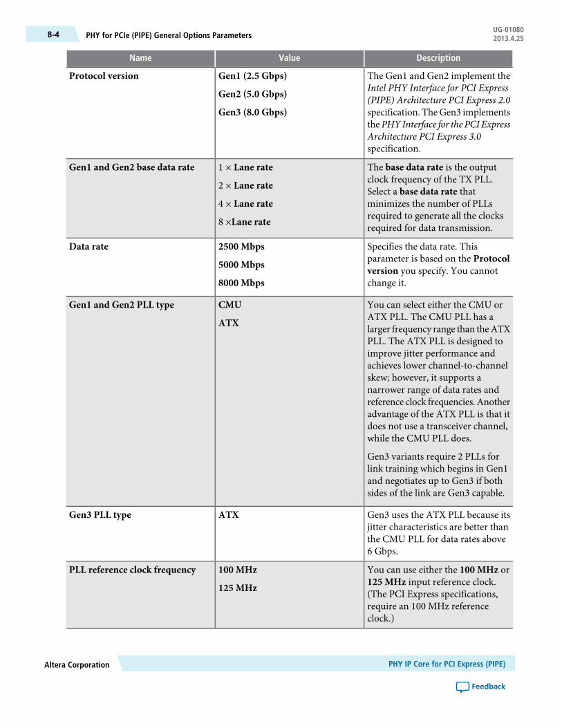
DescriptionValueName
The Gen1 and Gen2 implement theIntel PHY Interface for PCI Express(PIPE) Architecture PCI Express 2.0specification. TheGen3 implementsthePHY Interface for the PCI ExpressArchitecture PCI Express 3.0specification.
Gen1 (2.5 Gbps)
Gen2 (5.0 Gbps)
Gen3 (8.0 Gbps)
Protocol version
The base data rate is the outputclock frequency of the TX PLL.Select a base data rate thatminimizes the number of PLLsrequired to generate all the clocksrequired for data transmission.
1 × Lane rate
2 × Lane rate
4 × Lane rate
8 ×Lane rate
Gen1 and Gen2 base data rate
Specifies the data rate. Thisparameter is based on the Protocolversion you specify. You cannotchange it.
2500 Mbps
5000 Mbps
8000 Mbps
Data rate
You can select either the CMU orATX PLL. The CMU PLL has alarger frequency range than theATXPLL. The ATX PLL is designed toimprove jitter performance andachieves lower channel-to-channelskew; however, it supports anarrower range of data rates andreference clock frequencies. Anotheradvantage of the ATX PLL is that itdoes not use a transceiver channel,while the CMU PLL does.
Gen3 variants require 2 PLLs forlink training which begins in Gen1and negotiates up to Gen3 if bothsides of the link are Gen3 capable.
CMU
ATX
Gen1 and Gen2 PLL type
Gen3 uses the ATX PLL because itsjitter characteristics are better thanthe CMU PLL for data rates above6 Gbps.
ATXGen3 PLL type
You can use either the 100 MHz or125 MHz input reference clock.(The PCI Express specifications,require an 100 MHz referenceclock.)
100 MHz
125 MHz
PLL reference clock frequency
PHY IP Core for PCI Express (PIPE)Altera Corporation
Feedback
UG-01080PHY for PCIe (PIPE) General Options Parameters8-4 2013.4.25
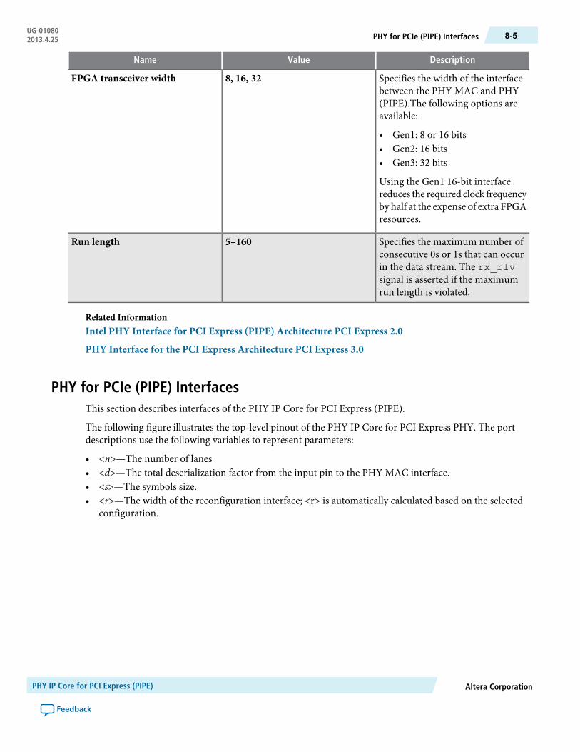
DescriptionValueName
Specifies the width of the interfacebetween the PHY MAC and PHY(PIPE).The following options areavailable:
• Gen1: 8 or 16 bits• Gen2: 16 bits• Gen3: 32 bits
Using the Gen1 16-bit interfacereduces the required clock frequencyby half at the expense of extra FPGAresources.
8, 16, 32FPGA transceiver width
Specifies the maximum number ofconsecutive 0s or 1s that can occurin the data stream. The rx_rlvsignal is asserted if the maximumrun length is violated.
5–160Run length
Related InformationIntel PHY Interface for PCI Express (PIPE) Architecture PCI Express 2.0
PHY Interface for the PCI Express Architecture PCI Express 3.0
PHY for PCIe (PIPE) InterfacesThis section describes interfaces of the PHY IP Core for PCI Express (PIPE).
The following figure illustrates the top-level pinout of the PHY IP Core for PCI Express PHY. The portdescriptions use the following variables to represent parameters:
• <n>—The number of lanes• <d>—The total deserialization factor from the input pin to the PHY MAC interface.• <s>—The symbols size.• <r>—The width of the reconfiguration interface; <r> is automatically calculated based on the selected
configuration.
Altera CorporationPHY IP Core for PCI Express (PIPE)
Feedback
8-5PHY for PCIe (PIPE) InterfacesUG-010802013.4.25
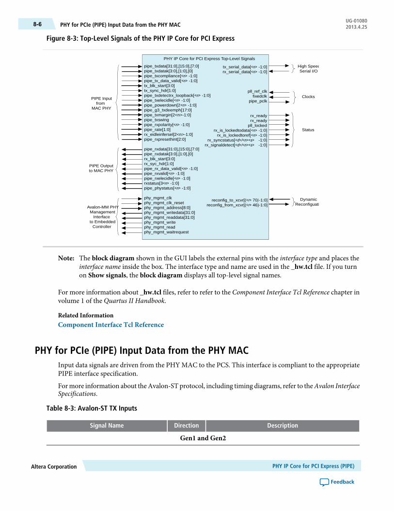
Figure 8-3: Top-Level Signals of the PHY IP Core for PCI Express
PHY IP Core for PCI Express Top-Level Signals
tx_serial_data[<n> -1:0]rx_serial_data[<n> -1:0]
pll_ref_clkfixedclk
pipe_pclk
rx_readyrx_ready
pll_lockedrx_is_lockedtodata[<n> -1:0]
rx_is_lockedtoref[<n> -1:0]rx_syncstatus[<d>/<n><s> -1:0]
rx_signaldetect[<d>/<n><s> -1:0]
High SpeedSerial I/O
Avalon-MM PHYManagement
Interfaceto Embedded
Controller
PIPE Inputfrom
MAC PHY
PIPE Outputto MAC PHY
Clocks
Status
pipe_txdata[31:0],[15:0],[7:0]pipe_txdatak[3:0],[1:0],[0]pipe_txcompliance[<n> -1:0]pipe_tx_data_valid[<n> -1:0]tx_blk_start[3:0]tx_sync_hdr[1:0]pipe_txdetectrx_loopback[<n> -1:0]pipe_txelecidle[<n> -1:0]pipe_powerdown[2<n> -1:0]pipe_g3_txdeemph[17:0]pipe_txmargin[2<n>-1:0]pipe_txswingpipe_rxpolarity[<n> -1:0]pipe_rate[1:0]rx_eidleinfersel[2<n>-1:0]pipe_rxpresethint[2:0]
pipe_rxdata[31:0],[15:0],[7:0]pipe_rxdatak[3:0],[1:0],[0]rx_blk_start[3:0]rx_syc_hdr[1:0]pipe_rx_data_valid[<n> -1:0]pipe_rxvalid[<n> -1:0]pipe_rxelecidle[<n> -1:0]rxstatus[3<n> -1:0]pipe_phystatus[<n> -1:0]
phy_mgmt_clkphy_mgmt_clk_resetphy_mgmt_address[8:0]phy_mgmt_writedata[31:0]phy_mgmt_readdata[31:0]phy_mgmt_writephy_mgmt_readphy_mgmt_waitrequest
reconfig_to_xcvr[(<r> 70)-1:0]reconfig_from_xcvr[(<r> 46)-1:0]
DynamicReconfiguation
The block diagram shown in the GUI labels the external pins with the interface type and places theinterface name inside the box. The interface type and name are used in the _hw.tcl file. If you turnon Show signals, the block diagram displays all top-level signal names.
Note:
For more information about _hw.tcl files, refer to refer to the Component Interface Tcl Reference chapter involume 1 of the Quartus II Handbook.
Related InformationComponent Interface Tcl Reference
PHY for PCIe (PIPE) Input Data from the PHY MACInput data signals are driven from the PHY MAC to the PCS. This interface is compliant to the appropriatePIPE interface specification.
Formore information about theAvalon-ST protocol, including timing diagrams, refer to theAvalon InterfaceSpecifications.
Table 8-3: Avalon-ST TX Inputs
DescriptionDirectionSignal Name
Gen1 and Gen2
PHY IP Core for PCI Express (PIPE)Altera Corporation
Feedback
UG-01080PHY for PCIe (PIPE) Input Data from the PHY MAC8-6 2013.4.25

DescriptionDirectionSignal Name
Parallel PCI Express data input bus. For the 16-bitinterface, 16 bits represent 2 symbols of transmit data.Bits [7:0] is transmitted first; bits[15:8] are transmittedsecond. Bit 0 if the first to be transmitted. For the32-bit interface, 32 bits represent the 4 symbols of TXdata. Bits[23:16] are the third symbol to be transmittedand bits [31:24] are the fourth symbol.
Inputpipe_txdata[31:0],[15:0], or[7:0]
For Gen1 and Gen2, data and control indicator forthe received data. When 0, indicates that pipe_txdatais data, when 1, indicates that pipe_txdata iscontrol.
For Gen3, Bit[0] corresponds to pipe_txdata[7:0], bit[1] corresponds to pipe_txdata[15:8], and so on.
Inputpipe_txdatak[(3:0],[1:0] or[0]
Asserted for one cycle to set the running disparity tonegative. Used when transmitting the compliancepattern. Refer to section 6.11 of the Intel PHY Interfacefor PCI Express (PIPE) Architecture for moreinformation.
Inputpipe_txcompliance
For Gen3, specifies start block byte location for TXdata in the 128-bit block data. Usedwhen the interfacebetween the PCS and PHY MAC is 32 bits. Not usedfor the Gen1 and Gen2 data rates.
Inputtx_blk_start
For Gen3, indicates whether the 130-bit block beingtransmitted is a Data or Control Ordered Set Block.The following encodings are defined:
• 2'b10: Data block• 2'b01: Control Ordered Set Block
This value is read when tx_blk_start = 1b’1.Refer to “Section 4.2.2.1. Lane Level Encoding” in thePCI Express Base Specification, Rev. 3.0 for a detailedexplanation of data transmission and reception using128b/130b encoding and decoding. Not used for theGen1 and Gen2 data rates.
Inputtx_sync_hdr[1:0]
This signal instructs the PHY to start a receivedetection operation. After power-up asserting thissignal starts a loopback operation. Refer to section 6.4of the Intel PHY Interface for PCI Express (PIPE) fora timing diagram.
Inputpipe_txdetectrx_loopback
Altera CorporationPHY IP Core for PCI Express (PIPE)
Feedback
8-7PHY for PCIe (PIPE) Input Data from the PHY MACUG-010802013.4.25
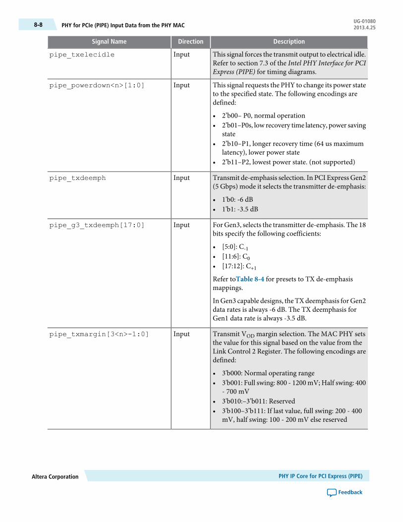
DescriptionDirectionSignal Name
This signal forces the transmit output to electrical idle.Refer to section 7.3 of the Intel PHY Interface for PCIExpress (PIPE) for timing diagrams.
Inputpipe_txelecidle
This signal requests the PHY to change its power stateto the specified state. The following encodings aredefined:
• 2’b00– P0, normal operation• 2’b01–P0s, low recovery time latency, power saving
state• 2’b10–P1, longer recovery time (64 us maximum
latency), lower power state• 2’b11–P2, lowest power state. (not supported)
Inputpipe_powerdown<n>[1:0]
Transmit de-emphasis selection. In PCI Express Gen2(5 Gbps) mode it selects the transmitter de-emphasis:
• 1'b0: -6 dB• 1'b1: -3.5 dB
Inputpipe_txdeemph
ForGen3, selects the transmitter de-emphasis. The 18bits specify the following coefficients:
• [5:0]: C-1• [11:6]: C0• [17:12]: C+1
Refer toTable 8-4 for presets to TX de-emphasismappings.
InGen3 capable designs, the TXdeemphasis forGen2data rates is always -6 dB. The TX deemphasis forGen1 data rate is always -3.5 dB.
Inputpipe_g3_txdeemph[17:0]
Transmit VOD margin selection. The MAC PHY setsthe value for this signal based on the value from theLink Control 2 Register. The following encodings aredefined:
• 3'b000: Normal operating range• 3'b001: Full swing: 800 - 1200 mV; Half swing: 400
- 700 mV• 3'b010:–3’b011: Reserved• 3'b100–3’b111: If last value, full swing: 200 - 400
mV, half swing: 100 - 200 mV else reserved
Inputpipe_txmargin[3<n>-1:0]
PHY IP Core for PCI Express (PIPE)Altera Corporation
Feedback
UG-01080PHY for PCIe (PIPE) Input Data from the PHY MAC8-8 2013.4.25
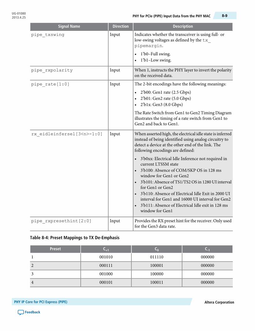
DescriptionDirectionSignal Name
Indicates whether the transceiver is using full- orlow-swing voltages as defined by the tx_pipemargin.
• 1’b0–Full swing.• 1’b1–Low swing.
Inputpipe_txswing
When 1, instructs the PHY layer to invert the polarityon the received data.
Inputpipe_rxpolarity
The 2-bit encodings have the following meanings:
• 2’b00: Gen1 rate (2.5 Gbps)• 2’b01: Gen2 rate (5.0 Gbps)• 2’b1x: Gen3 (8.0 Gbps)
The Rate Switch from Gen1 to Gen2 Timing Diagramillustrates the timing of a rate switch from Gen1 toGen2 and back to Gen1.
Inputpipe_rate[1:0]
When asserted high, the electrical idle state is inferredinstead of being identified using analog circuitry todetect a device at the other end of the link. Thefollowing encodings are defined:
• 3'b0xx: Electrical Idle Inference not required incurrent LTSSM state
• 3'b100: Absence of COM/SKP OS in 128 mswindow for Gen1 or Gen2
• 3'b101: Absence of TS1/TS2OS in 1280UI intervalfor Gen1 or Gen2
• 3'b110: Absence of Electrical Idle Exit in 2000 UIinterval for Gen1 and 16000 UI interval for Gen2
• 3'b111: Absence of Electrical Idle exit in 128 mswindow for Gen1
Inputrx_eidleinfersel[3<n>-1:0]
Provides the RX preset hint for the receiver. Only usedfor the Gen3 data rate.
Inputpipe_rxpresethint[2:0]
Table 8-4: Preset Mappings to TX De-Emphasis
C-1C0C+1Preset
0000000111100010101
0000001000010001112
0000001000000010003
0000001000110001014
Altera CorporationPHY IP Core for PCI Express (PIPE)
Feedback
8-9PHY for PCIe (PIPE) Input Data from the PHY MACUG-010802013.4.25

C-1C0C+1Preset
0000001010000000005
0001001001000000006
0001011000110000007
0001000110000010008
0001010111100001019
00011110000100000010
00000001110000110011
Related InformationAvalon Interface Specifications
Intel PHY Interface for PCI Express (PIPE) Architecture
PCI Express Base Specification, Rev. 3.
PHY for PCIe (PIPE) Output Data to the PHY MACThis section describes the PIPE output signals. These signals are driven from the PCS to the PHY MAC.This interface is compliant to the appropriate PIPE interface specification.
Table 8-5: Avalon-ST RX Inputs
DescriptionDirectionSignal Name
This is RX parallel data driven from the PCS to the MACPHY. The ready latency on this interface is 0, so that theMAC must be able to accept data as soon as the PHY comesout of reset. Width is 8 or 16 for Gen1 and Gen2. Width is32 for Gen3.
Transmission is little endian. For example, for Gen3, wordsare transmitted in the following order:
• PIPE word 0: pipe_rxdata[7:0]• PIPE word 1: pipe_rxdata[15:8]• PIPE word 2: pipe_rxdata[23:16]• PIPE word 3: pipe_rxdata[31:24]
Outputpipe_rxdata[[(31,16or8)-1:0]
Data and control indicator for the source data. When 0,indicates that pipe_rxdata is data, when 1, indicatesthat pipe_rxdata is control.
Bit[0] corresponds to byte 0. Bit[]1 corresponds to byte 1,and so on.
Outputpipe_rxdatak[(3,2 or 1)-1:0]
PHY IP Core for PCI Express (PIPE)Altera Corporation
Feedback
UG-01080PHY for PCIe (PIPE) Output Data to the PHY MAC8-10 2013.4.25
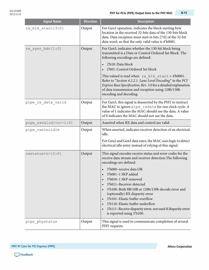
DescriptionDirectionSignal Name
For Gen3 operation, indicates the block starting bytelocation in the received 32-bits data of the 130-bits blockdata. Data reception must start in bits [7:0] of the 32-bitdata word, so that the only valid value is 4’b0001.
Outputrx_blk_start[3:0]
For Gen3, indicates whether the 130-bit block beingtransmitted is a Data or Control Ordered Set Block. Thefollowing encodings are defined:
• 2'b10: Data block• 2'b01: Control Ordered Set block
This valued is read when rx_blk_start = 4'b0001.Refer to “Section 4.2.2.1. Lane Level Encoding” in the PCIExpress Base Specification, Rev. 3.0 for a detailed explanationof data transmission and reception using 128b/130bencoding and decoding.
Outputrx_sync_hdr[1:0]
For Gen3, this signal is deasserted by the PHY to instructthe MAC to ignore pipe_rxdata for one clock cycle. Avalue of 1 indicates the MAC should use the data. A valueof 0 indicates the MAC should not use the data.
Outputpipe_rx_data_valid
Asserted when RX data and control are valid.Outputpipe_rxvalid[<n>-1:0]
When asserted, indicates receiver detection of an electricalidle.
For Gen2 and Gen3 data rates, the MAC uses logic to detectelectrical idle entry instead of relying of this signal.
Outputpipe_rxelecidle
This signal encodes receive status and error codes for thereceive data stream and receiver detection.The followingencodings are defined:
• 3’b000–receive data OK• 3’b001–1 SKP added• 3’b010–1 SKP removed• 3’b011–Receiver detected• 3’b100–Both 8B/10B or 128b/130b decode error and
(optionally) RX disparity error• 3’b101–Elastic buffer overflow• 3’b110–Elastic buffer underflow• 3’b111–Receive disparity error, not used if disparity error
is reported using 3’b100.
Outputrxstatus<n>[2:0]
This signal is used to communicate completion of severalPHY requests.
Outputpipe_phystatus
Altera CorporationPHY IP Core for PCI Express (PIPE)
Feedback
8-11PHY for PCIe (PIPE) Output Data to the PHY MACUG-010802013.4.25

Figure 8-4: Rate Switch from Gen1 to Gen2 Timing Diagram
In the figure, Time T1 is pending characterization and <n> is the number of lanes.
pipe_pclk
pipe_rate[1:0] 0 1 0 2
T1 T1 T1
62.5 MHz (Gen1) 62.5 MHz (Gen1) 250 MHz (Gen3)125 MHz (Gen2)
pipe_phystatus[<n>-1:0]
Related InformationPCI Express Base Specification, Rev. 3.0
PHY for PCIe (PIPE) ClocksThis section describes the clock ports.
Table 8-6: Clock Ports
DescriptionDirectionSignal Name
This is the 100 MHz input reference clock source for thePHYTXandRXPLL. You can optionally provide a 125MHzinput reference clock by setting the PLL reference clockfrequency parameter to 125 MHz as described in PHY IPCore for PCI Express General Options.
Inputpll_ref_clk
A 100 MHz or 125 MHz clock used for the receiver detectcircuitry. This clock can be derived from pll_ref_clk.
Inputfixedclk
Generated in the PMAanddriven to theMACPHY interface.All data and status signals are synchronous topipe_pclk.This clock has the following frequencies:
• Gen1: 62.5 MHz• Gen2:125 MHz• Gen3: 250 MHz
Outputpipe_pclk
The following table lists the pipe_pclk frequencies for all available PCS interface widths. Doubling theFPGA transceiver width haves the required frequency.
Table 8-7: pipe_pclk Frequencies
Gen3Gen2Gen1FPGA Transceiver WidthCapability
——250 MHz8 bitsGen1 only
——125 MHz16 bits
PHY IP Core for PCI Express (PIPE)Altera Corporation
Feedback
UG-01080PHY for PCIe (PIPE) Clocks8-12 2013.4.25

Gen3Gen2Gen1FPGA Transceiver WidthCapability
—250 MHz125 MHz16 bitsGen2 capable
250 MHz125 MHz62.5 MHz32 bitsGen3 capable
PHY for PCIe (PIPE) Clock SDC Timing Constraints for Gen3 DesignsFor Gen3 designs, you must add the following timing constraints to force Timequest to analyze the designat Gen1, Gen2 and Gen3 data rates. Include these constraints in your top-level SDC file for the project.
Add the following command to force Timequest analysis at 250 MHz.
create_generated_clock -name clk_g3 -source [get_ports {pll_refclk}]\-divide_by 2 -multiply_by 5 -duty_cycle 50 -phase 0 -offset 0 [get_nets
{*pipe_nr_inst|transceiver_core|inst_sv_xcvr_native|inst_sv_pcs|\|ch[*].inst_sv_pcs_ch|inst_sv_hssi_tx_pld_pcs_interface|pld8gtxclkout}]-add
Add the following command to force Timequest analysis at 62.5 MHz.
create_generated_clock -name clk_g3 -source [get_ports {pll_refclk}]\-divide_by 8 -multiply_by 5 -duty_cycle 50 -phase 0 -offset 0 [get_nets\
{*pipe_nr_inst|transceiver_core|inst_sv_xcvr_native|inst_sv_pcs| \ch[*].inst_sv_pcs_ch|inst_sv_hssi_tx_pld_pcs_interface|pld8gtxclkout}]-add
#creating false paths between these clock groupsset_clock_groups -asynchronous -group [get_clocks clk_g3]set_clock_groups -asynchronous -group [get_clocks clk_g1]set_clock_groups -asynchronous -group [get_clocks *pipe_nr_inst| \transceiver_core|inst_sv_xcvr_native|inst_sv_pcs|ch[*]. \inst_sv_pcs_ch|inst_sv_hssi_8g_tx_pcs|wys|clkout]
PHY for PCIe (PIPE) Optional Status InterfaceThis section describes the signals the optional status signals.
Altera CorporationPHY IP Core for PCI Express (PIPE)
Feedback
8-13PHY for PCIe (PIPE) Clock SDC Timing Constraints for Gen3 DesignsUG-010802013.4.25

Table 8-8: Status Signals
Signal NameDirectionSignal Name 4
When asserted, indicates that the TX interface has exitedthe reset state and is ready to transmit.
Outputtx_ready
When asserted, indicates that the RX interface has exitedthe reset state and is ready to receive.
Outputrx_ready
When asserted, indicates that the TX PLL is locked to theinput reference clock. This signal is asynchronous.
Outputpll_locked[<p>-1:0]
When asserted, the receiver CDR is in to lock-to-datamode. When deasserted, the receiver CDR lock modedepends on the rx_locktorefclk signal level.
Outputrx_is_lockedtodata[<n>-1:0]
Asserted when the receiver CDR is locked to the inputreference clock. This signal is asynchronous.
Outputrx_is_lockedtoref[<n>-1:0]
Indicates presence or absence of synchronization on theRX interface. Asserted when word aligner identifies theword alignment pattern or synchronization code groupsin the received data stream.
Outputrx_syncstatus[<d><n>/8-1:0]
When asserted indicates that the lane detects a sender atthe other end of the link.
Outputrx_signaldetect[<d><n>/8-1:0]
PHY for PCIe (PIPE) Serial Data InterfaceThis section describes the differential serial TX and RX connections to FPGA pins.
Table 8-9: Transceiver Differential Serial Interface
DescriptionDirectionSignal Name
Receiver differential serial input data, <n> is the numberof lanes.
Inputrx_serial_data[<n>-1:0]
Transmitter differential serial output data <n> is thenumber of lanes.
Outputtx_serial_data[<n>-1:0]
For information about channel placement, refer to “TransceiverClocking andChannel PlacementGuidelines”in the Transceiver Configurations in Arria V GZ Devices or “Transceiver Clocking and Channel PlacementGuidelines” in the Transceiver Configurations in Stratix V Devices as appropriate.
For soft IP implementations of PCI Express, channel placement is determined by the Quartus IIfitter.
Note:
For information about channel placement of theHard IP PCI Express IPCore, refer to theChannel PlacementGen1 and Gen2 and Channel Placement Gen3 sections in the Stratix V Hard IP for PCI Express User Guide.
4 <n> is the number of lanes. <d> is the deserialization factor. < p> is the number of PLLs.
PHY IP Core for PCI Express (PIPE)Altera Corporation
Feedback
UG-01080PHY for PCIe (PIPE) Serial Data Interface8-14 2013.4.25
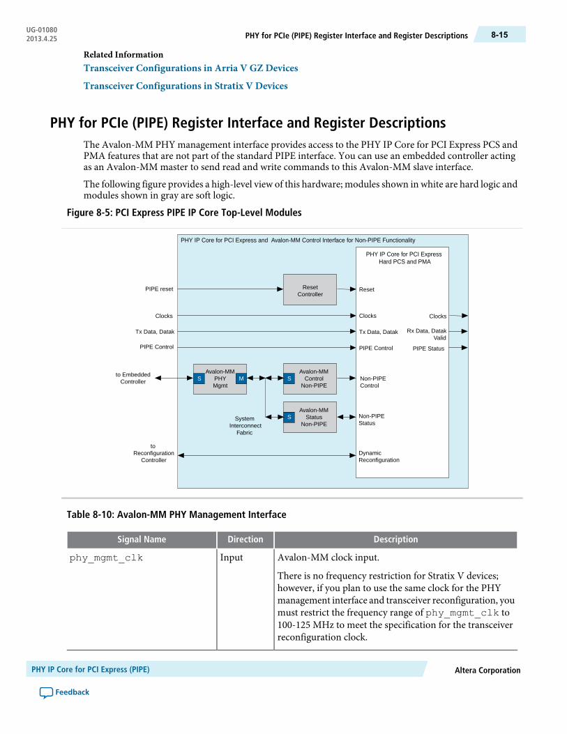
Related InformationTransceiver Configurations in Arria V GZ Devices
Transceiver Configurations in Stratix V Devices
PHY for PCIe (PIPE) Register Interface and Register DescriptionsThe Avalon-MM PHY management interface provides access to the PHY IP Core for PCI Express PCS andPMA features that are not part of the standard PIPE interface. You can use an embedded controller actingas an Avalon-MM master to send read and write commands to this Avalon-MM slave interface.
The following figure provides a high-level view of this hardware; modules shown in white are hard logic andmodules shown in gray are soft logic.
Figure 8-5: PCI Express PIPE IP Core Top-Level Modules
SystemInterconnect
Fabric
to EmbeddedController
toReconfiguration
Controller
Clocks
Tx Data, Datak
PIPE Control
PHY IP Core for PCI ExpressHard PCS and PMA
PHY IP Core for PCI Express and Avalon-MM Control Interface for Non-PIPE Functionality
DynamicReconfiguration
PIPE Control
Tx Data, Datak
Clocks
PIPE Status
Rx Data, DatakValid
Clocks
Reset
Non-PIPEStatus
Non-PIPEControl
SAvalon-MM
ControlNon-PIPE
SAvalon-MM
StatusNon-PIPE
ResetController
PIPE reset
MAvalon-MM
PHYMgmt
S
Table 8-10: Avalon-MM PHY Management Interface
DescriptionDirectionSignal Name
Avalon-MM clock input.
There is no frequency restriction for Stratix V devices;however, if you plan to use the same clock for the PHYmanagement interface and transceiver reconfiguration, youmust restrict the frequency range of phy_mgmt_clk to100-125 MHz to meet the specification for the transceiverreconfiguration clock.
Inputphy_mgmt_clk
Altera CorporationPHY IP Core for PCI Express (PIPE)
Feedback
8-15PHY for PCIe (PIPE) Register Interface and Register DescriptionsUG-010802013.4.25
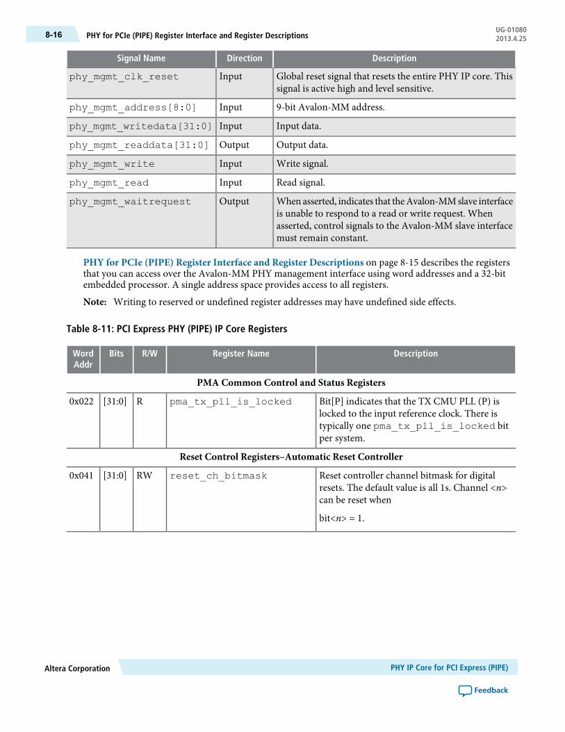
DescriptionDirectionSignal Name
Global reset signal that resets the entire PHY IP core. Thissignal is active high and level sensitive.
Inputphy_mgmt_clk_reset
9-bit Avalon-MM address.Inputphy_mgmt_address[8:0]
Input data.Inputphy_mgmt_writedata[31:0]
Output data.Outputphy_mgmt_readdata[31:0]
Write signal.Inputphy_mgmt_write
Read signal.Inputphy_mgmt_read
Whenasserted, indicates that theAvalon-MMslave interfaceis unable to respond to a read or write request. Whenasserted, control signals to the Avalon-MM slave interfacemust remain constant.
Outputphy_mgmt_waitrequest
PHY for PCIe (PIPE) Register Interface and Register Descriptions on page 8-15 describes the registersthat you can access over the Avalon-MM PHY management interface using word addresses and a 32-bitembedded processor. A single address space provides access to all registers.
Writing to reserved or undefined register addresses may have undefined side effects.Note:
Table 8-11: PCI Express PHY (PIPE) IP Core Registers
DescriptionRegister NameR/WBitsWordAddr
PMA Common Control and Status Registers
Bit[P] indicates that the TX CMU PLL (P) islocked to the input reference clock. There istypically one pma_tx_pll_is_locked bitper system.
pma_tx_pll_is_lockedR[31:0]0x022
Reset Control Registers–Automatic Reset Controller
Reset controller channel bitmask for digitalresets. The default value is all 1s. Channel <n>can be reset when
bit<n> = 1.
reset_ch_bitmaskRW[31:0]0x041
PHY IP Core for PCI Express (PIPE)Altera Corporation
Feedback
UG-01080PHY for PCIe (PIPE) Register Interface and Register Descriptions8-16 2013.4.25
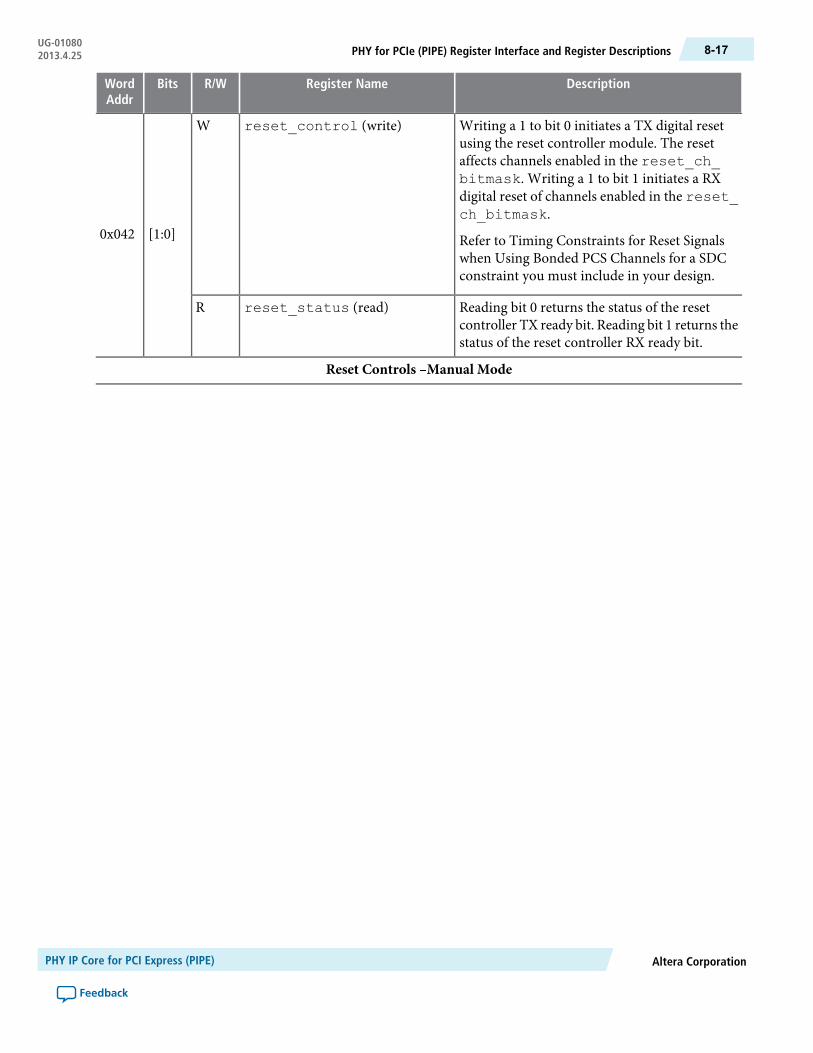
DescriptionRegister NameR/WBitsWordAddr
Writing a 1 to bit 0 initiates a TX digital resetusing the reset controller module. The resetaffects channels enabled in the reset_ch_bitmask. Writing a 1 to bit 1 initiates a RXdigital reset of channels enabled in the reset_ch_bitmask.
Refer to Timing Constraints for Reset Signalswhen Using Bonded PCS Channels for a SDCconstraint you must include in your design.
reset_control (write)W
[1:0]0x042
Reading bit 0 returns the status of the resetcontroller TX ready bit. Reading bit 1 returns thestatus of the reset controller RX ready bit.
reset_status (read)R
Reset Controls –Manual Mode
Altera CorporationPHY IP Core for PCI Express (PIPE)
Feedback
8-17PHY for PCIe (PIPE) Register Interface and Register DescriptionsUG-010802013.4.25

DescriptionRegister NameR/WBitsWordAddr
You can use the reset_fine_controlregister to create your own reset sequence. Thereset control module, illustrated in TransceiverPHY Top-Level Modules, performs a standardreset sequence at power on and whenever thephy_mgmt_clk_reset is asserted.Bits [31:4,0] are reserved.
reset_fine_controlRW[31:0]
0x044
It is safe to write 0s to reserved bits.ReservedRW[31:4]
Writing a 1 causes the RX digital reset signal tobe asserted, resetting the RX digital channelsenabled in reset_ch_bitmask. You mustwrite a 0 to clear the reset condition.
reset_rx_digitalRW[3]
Writing a 1 causes the internal RX digital resetsignal to be asserted, resetting the RX analog logicof all channels enabled in reset_ch_bitmask. You must write a 0 to clear the resetcondition.
reset_rx_analogRW[2]
Writing a 1 causes the internal TX digital resetsignal to be asserted, resetting all channelsenabled in reset_ch_bitmask. You mustwrite a 0 to clear the reset condition.
Refer to Timing Constraints for Reset Signalswhen Using Bonded PCS Channels for a SDCconstraint you must include in your design.
reset_tx_digitalRW[1]
Writing a 1 causes the internal TX PLL topowerdown. If you reset the transceiver, youmust assert pll_powerdown by writing a 1 tothis register and then writing a 0 after 1 ms.
pll_powerdownRW[0]
PMA Control and Status Registers
Writing a 1 to channel <n> puts channel <n> inserial loopback mode.
phy_serial_loopbackRW[31:0]0x061
When channel <n> =1, indicates that receivecircuit for channel <n> senses the specifiedvoltage exists at the RX input buffer. This optionis only operational for the PCI Express PHY IPCore.
pma_rx_signaldetectR[31:0]0x063
When set, programs the RX CDR PLL to lock tothe incoming data. Bit <n> corresponds tochannel <n>.
pma_rx_set_locktodataRW[31:0]0x064
PHY IP Core for PCI Express (PIPE)Altera Corporation
Feedback
UG-01080PHY for PCIe (PIPE) Register Interface and Register Descriptions8-18 2013.4.25

DescriptionRegister NameR/WBitsWordAddr
When set, programs the RX CDR PLL to lock tothe reference clock. Bit <n> corresponds tochannel <n>.
pma_rx_set_locktorefRW[31:0]0x065
When asserted, indicates that the RX CDR PLLis locked to the RX data, and that the RX CDRhas changed from LTR to LTD mode. Bit <n>corresponds to channel <n>.
pma_rx_is_lockedtodataR[31:0]0x066
When asserted, indicates that the RX CDR PLLis locked to the reference clock. Bit <n>corresponds to channel <n>.
pma_rx_is_lockedtorefR[31:0]0x067
PCS for PCI Express
Specifies lane or group number for indirectaddressing, which is used for all PCS control andstatus registers. For variants that stripe dataacross multiple lanes, this is the logical groupnumber. For non-bonded applications, this is thelogical lane number.
Lane or group numberRW[31:0]0x080
—ReservedR[31:6]
0x081
Records the number of bits slipped by the RXWord Aligner to achieve word alignment. Usedfor very latency sensitive protocols.
From block: Word aligner.
rx_bitslipboundaryselectout
R[5:1]
When set, indicates an RX phase compensationFIFO error.
From block: RX phase compensation FIFO.
rx_phase_comp_fifo_errorR[0]
—ReservedR[31:1]
0x082When set, indicates a TX phase compensationFIFO error.
From block: TX phase compensation FIFO.
tx_phase_comp_fifo_errorRW[0]
Altera CorporationPHY IP Core for PCI Express (PIPE)
Feedback
8-19PHY for PCIe (PIPE) Register Interface and Register DescriptionsUG-010802013.4.25
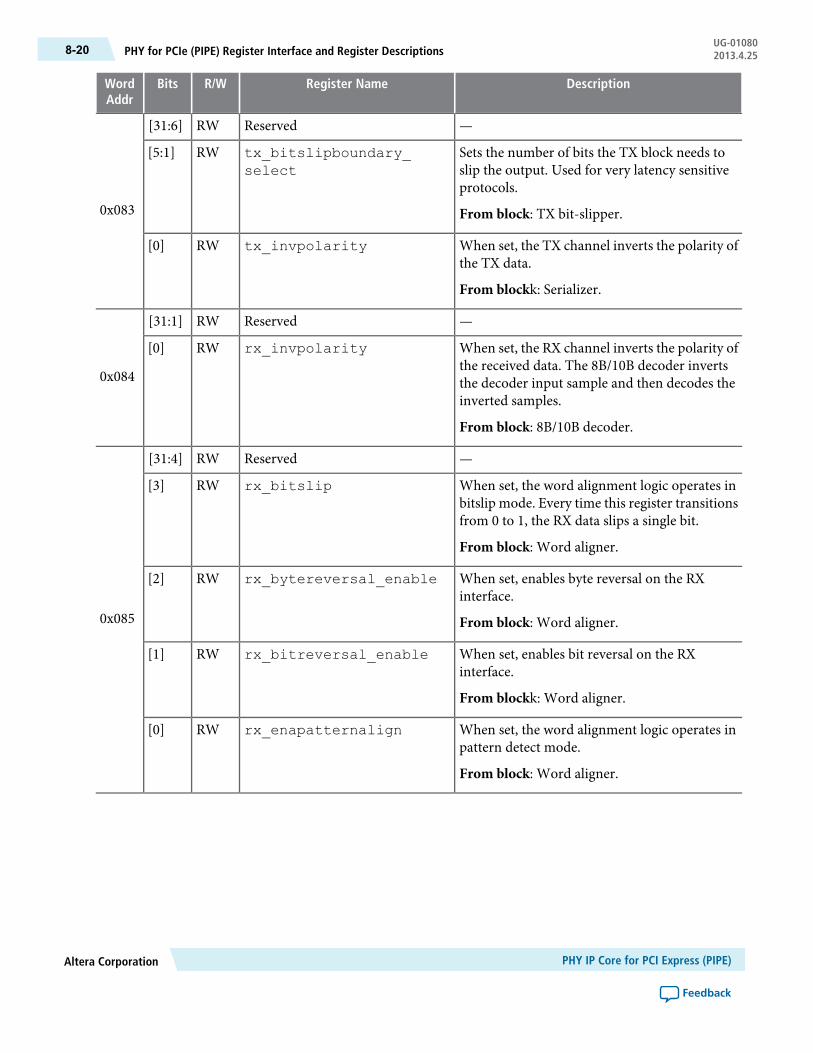
DescriptionRegister NameR/WBitsWordAddr
—ReservedRW[31:6]
0x083
Sets the number of bits the TX block needs toslip the output. Used for very latency sensitiveprotocols.
From block: TX bit-slipper.
tx_bitslipboundary_select
RW[5:1]
When set, the TX channel inverts the polarity ofthe TX data.
From blockk: Serializer.
tx_invpolarityRW[0]
—ReservedRW[31:1]
0x084
When set, the RX channel inverts the polarity ofthe received data. The 8B/10B decoder invertsthe decoder input sample and then decodes theinverted samples.
From block: 8B/10B decoder.
rx_invpolarityRW[0]
—ReservedRW[31:4]
0x085
When set, the word alignment logic operates inbitslip mode. Every time this register transitionsfrom 0 to 1, the RX data slips a single bit.
From block: Word aligner.
rx_bitslipRW[3]
When set, enables byte reversal on the RXinterface.
From block: Word aligner.
rx_bytereversal_enableRW[2]
When set, enables bit reversal on the RXinterface.
From blockk: Word aligner.
rx_bitreversal_enableRW[1]
When set, the word alignment logic operates inpattern detect mode.
From block: Word aligner.
rx_enapatternalignRW[0]
PHY IP Core for PCI Express (PIPE)Altera Corporation
Feedback
UG-01080PHY for PCIe (PIPE) Register Interface and Register Descriptions8-20 2013.4.25

DescriptionRegister NameR/WBitsWordAddr
—ReservedR[31:20]
0x086
When set, indicates a run length violation.
From block: Word aligner.
rx_rlvR[19:16]
When set, indicates that RX word aligner hasachieved synchronization.
From block: Word aligner.
rx_patterndetectR[15:12]
When set, indicates that the received 10-bit codeor data group has a disparity error. When set, thecorresponding errdetect bits are also set.
From block: 8B/10B decoder.
rx_disperrR[11:8]
When set, indicates that the RX interface issynchronized to the incoming data.
From block: Word aligner.
rx_syncstatusR[7:4]
When set, indicates that a received 10-bit codegroup has an 8B/10B code violation or disparityerror. It is used along with RX disparity todifferentiate between a code violation error anda disparity error, or both.
In PIPE mode, the PIPE specific output portcalled pipe_rxstatus encodes the errors.
From block: 8B/10B decoder.
rx_errdetectR[3:0]
For more information about the individual PCS blocks, refer toTransceiver Architecture in Stratix VDevicesin the Stratix V Device Handbook.
Related InformationTransceiver Architecture in Stratix V Devices
PHY for PCIe (PIPE) Link Equalization for Gen3 Data RateGen3 requires both TX and RX link equalization because of the data rate, the channel characteristics, receiverdesign, and process variations. The link equalization process allows the Endpoint and Root Port to adjustthe TX and RX setup of each lane to improve signal quality. This process results in Gen3 links with a receiverBit Error Rate (BER) that is less than 10-12.
“Section 4.2.3 Link Equalization Procedure for 8.0 GT/s Data Rate” in the PCI Express Base Specification, Rev.3.0 provides detailed information about the four-stage link equalization procedure. A new LTSSM state,Recovery.Equalization with Phases 0–3, reflects progress through Gen3 equalization. Phases 2 and 3 of link
Altera CorporationPHY IP Core for PCI Express (PIPE)
Feedback
8-21PHY for PCIe (PIPE) Link Equalization for Gen3 Data RateUG-010802013.4.25

equalization are optional; however, the link must progress through all four phases, even if no adjustmentsoccur. Skipping Phases 2 and 3 speeds up link training at the expense of link BER optimization.
Related InformationPHY Interface for the PCI Express Architecture PCI Express 3.0
Phase 0Phase 0 includes the following steps:
1. Upstream component enters Phase 0 of equalization during Recovery.Rcvrconfig by sending EQ TS2training sets with starting presets for the downstream component. EQ TS2 training sets may be sent at2.5 GT/s or 5 GT/s.
2. The downstream component enters Phase 0 of equalization after exiting Recovery.Speed at 8 GT/s. Itreceives the starting presets from the training sequences and applies them to its transmitter. At this time,upstream component has entered Phase 1 and is operating at 8 GT/s.
3. Tomove to Phase 1, the receivermust have a BER< 10-4 and should be able to decode enough consecutivetraining sequences.
4. The downstream component must detect training sets with Equalization Control (EC) bits set to 2’b01in order to move to EQ Phase 1.
Phase 1During Phase 1 of equalization process, the link partners exchange FS (Full Swing) and LF (Low Frequency)information. These values represent the upper and lower bounds for the TX coefficients. The receiver usesthis information to calculate and request the next set of transmitter coefficients.
1. Once training sets with EC bits set to 1’b0 are captured on all lanes, the upstream component moves toEQ Phase 2 sending EC=2’b10 along with starting pre-cursor, main cursor, and post-cursor coefficients.
2. The downstream component detects these new training sets, and moves to EQ Phase 2.
Phase 2 (Optional)This section describes the (optional) Phase 2.
During Phase 2, the Endpoint tunes the TX coefficients of the Root Port. The TS1 Use Preset bit determineswhether the Endpoint uses presets for coarse resolution or coefficients for fine resolution.
If you are using the PHY IP Core for PCI Express (PIPE) PCI Express as an Endpoint, you cannotperform Phase 2 tuning. The PIPE interface does not provide any measurement metric to the Root
Note:
Port to guide coefficient preset decision making. The Root Port should reflect the existing coefficientsand move to the next phase. The default Full Swing (FS) value advertized by Altera device is 40 andLow Frequency (LF) is 13.
If you are using the PHY IP Core for PCI Express (PIPE) PCI Express as Root Port, the End Point can tunethe Root Port TX coefficients.
The tuning sequence typically includes the following steps:
1. The Endpoint receives the starting presets from the Phase 2 training sets sent by the Root Port.2. The circuitry in the Endpoint receiver determines the BER and calculates the next set of transmitter
coefficients using FS and LF and embeds this information in the Training Sets for the Link Partner toapply to its transmitter.
PHY IP Core for PCI Express (PIPE)Altera Corporation
Feedback
UG-01080Phase 08-22 2013.4.25
The Root Port decodes these coefficients and presets, performs legality checks for the three transmittercoefficient rules and applies the settings to its transmitter and also sends them in the Training Sets. Threerules for transmitter coefficients are:
a. |C-1| <= Floor (FS/4)b. |C-1|+C0+|C+1| = FSc. C0-|C-1|-|C+1 |>= LF
Where:
C0 is the main cursor (boost)
C-1 is the pre-cursor (pre shoot)
C+1 is the post-cursor (de emphasis)
3. This process is repeated until the downstream component's receiver achieves a BER of < 10-12.
Phase 3 (Optional)This section describes the (optional) Phase 3.
During this phase, the Root Port tunes the Endpoint’s transmitter. This process is analogous to Phase 2 butoperates in the opposite direction.
If you are using the PHY IP Core for PCI Express (PIPE) PCI Express as a Root Port, you cannotperform Phase 3 tuning.
Note:
Once Phase 3 tuning is complete, the Root Port moves to Recovery.RcvrLock, sending EC=2’b00, along withthe final coefficients or preset agreed upon in Phase 2. The Endpoint moves to Recovery.RcvrLock using thefinal coefficients or preset agreed upon in Phase 3.
Recommendations for Tuning Link Partner’s TransmitterThis section describes tuning link partner’s transmitter.
To improve the BER of the StratixV receiver, Altera recommends that you turn on Adaptive Equalization(AEQ) one-time mode during Phase 2 Equalization for Endpoints or Phase 3 Equalization for Root Ports.You enable AEQ through the Transceiver Reconfiguration Controller IP Core. For more information aboutthis component, refer to Transceiver Reconfiguration Controller IP Core. For more information aboutrunning AEQ, refer to AEQ Registers.
AEQ must be turned off while switching from Gen3 to Gen1 or from Gen3 to Gen2.Note:
Enabling Dynamic PMA Tuning for PCIe Gen3“Section 4.2.3 Link Equalization Procedure for 8.0 GT/s Data Rate” in the PCI Express Base Specification,Rev. 3.0 provides detailed information about the four-stage link equalization procedure. However, in someinstances you may want to override the specified four-stage link equalization procedure to dynamically tunePMA settings. Follow these steps to override Gen3 equalization:
1. Connect the Transceiver Reconfiguration Controller IP Core to your PHY IP Core for PCI Express asshown in PCI Express PIPE IP Core Top-Level Modules.
Altera CorporationPHY IP Core for PCI Express (PIPE)
Feedback
8-23Phase 3 (Optional)UG-010802013.4.25

2. For each transmitter port, use the Quartus II Assignment Editor to assign the TransmitterVOD/Preemphasis Control Source the value RAM_CTL.
3. Recompile your design.
You can now use the Transceiver Reconfiguration Controller to change VOD and pre-emphasis settings.
Related InformationPHY Interface for the PCI Express Architecture PCI Express 3.0
PHY for PCIe (PIPE) Dynamic ReconfigurationDynamic reconfiguration calibrates each channel to compensate for variations due to process, voltage, andtemperature (PVT).
For Stratix V devices, each channel and each TX PLL have separate dynamic reconfiguration interfaces. TheMegaWizard Plug-In Manager provides informational messages on the connectivity of these interfaces. Thefollowing example shows the messages for a 8-channel PHY IP Core for PCI Express (PIPE).
Although you must initially create a separate reconfiguration interface for each channel and TX PLL in yourdesign, when the Quartus II software compiles your design, it reduces the total number of reconfigurationinterfaces by merging reconfiguration interfaces. The synthesized design typically includes a reconfigurationinterface for at least three channels because the three channels within each transceiver triplet share a singlephysical Avalon-MM slave interface which connects to the Transceiver Reconfiguration Controller IP Core.Conversely, you cannot connect the three channels that share this single physical Avalon-MM interface todifferent Transceiver Reconfiguration Controllers. Doing so causes a Fitter error. For more information,refer to“Transceiver Reconfiguration Controller to PHY IP Connectivity”.
Example 8-1: Informational Messages for the Transceiver Reconfiguration Interface
PHY IP will require 9 reconfiguration interfaces for connectionto the external reconfiguration controller.
Reconfiguration interface offsets 0-7 are connected to thetransceiver channels.
Reconfiguration interface offset 8 is connected to the transmitPLL.
The reconfiguration interface uses the Avalon-MM PHY Management interface clock.
Table 8-12: Reconfiguration Interface Signals
DescriptionDirectionSignal Name
Reconfiguration signals from the TransceiverReconfiguration Controller. <r> grows linearly with thenumber of reconfiguration interfaces.
Inputreconfig_to_xcvr [<r>70-1:0]
PHY IP Core for PCI Express (PIPE)Altera Corporation
Feedback
UG-01080PHY for PCIe (PIPE) Dynamic Reconfiguration8-24 2013.4.25

DescriptionDirectionSignal Name
Reconfiguration signals to the Transceiver ReconfigurationController. <r> grows linearly with the number ofreconfiguration interfaces.
Outputreconfig_from_xcvr [<r>46-1:0]
Logical Lane Assignment RestrictionIf you are using ×6 or ×N bonding, transceiver dynamic reconfiguration requires that you assign the startingchannel number.
Transceiver dynamic reconfiguration requires that you assign the starting channel number. For PCIe ×8configurations, logical channel 0 must be assigned to either physical transceiver channel 1 or channel 4 ofa transceiver bank. For PCIe x4 configurations, logical channel 1must be assigned to either physical transceiverchannel 1 or channel 4 of a transceiver bank. However, if you have already created a PCB with a differentlane assignment for PCIe ×8 logical lane 0 or PCIe ×4 logical lane 1, you can use the workaound shown inthe example below to remove this restriction; the example redefines thepma_bonding_master parameterusing the Quartus II Assignment Editor. In this example, the pma_bonding_master was originallyassigned to physical channel 1. (The original assignment could also have been to physical channel 4.) Theto parameter reassigns the pma_bonding_master to the PHY IP Core for PCI Express (PIPE) instancename. You must substitute the instance name from your design for the instance name shown in quotationmarks
Example 8-2: Overriding Logical Channel 0 Channel Assignment Restrictions in Stratix V Devicesfor ×6 or ×N Bonding
set_parameter -name pma_bonding_master "\"1\"" -to "<PHY IPinstance name>"
PHY for PCIe (PIPE) Simulation Files and Example TestbenchRefer to Running a Simulation Testbench for a description of the directories and files that the Quartus IIsoftware creates automatically when you generate your PHY IP Core for PCI Express.
Refer to the Altera Wiki for an example testbench that you can use as a starting point in creating your ownverification environment.
Related InformationAltera Wiki
Altera CorporationPHY IP Core for PCI Express (PIPE)
Feedback
8-25Logical Lane Assignment RestrictionUG-010802013.4.25
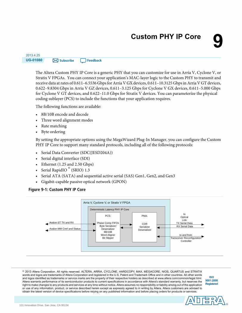
9Custom PHY IP Core
2013.4.25UG-01080 Subscribe Feedback
The Altera Custom PHY IP Core is a generic PHY that you can customize for use in Arria V, Cyclone V, orStratix V FPGAs. You can connect your application’s MAC-layer logic to the Custom PHY to transmit andreceive data at rates of 0.611–6.5536Gbps for Arria VGXdevices, 0.611–10.3125Gbps inArria VGTdevices,0.622–9.8304 Gbps in Arria V GZ devices, 0.611–3.125 Gbps for Cyclone V GX devices, 0.611–5.000 Gbpsfor Cyclone V GT devices, and 0.622–11.0 Gbps for Stratix V devices. You can parameterize the physicalcoding sublayer (PCS) to include the functions that your application requires.
The following functions are available:
• 8B/10B encode and decode• Three word alignment modes• Rate matching• Byte ordering
By setting the appropriate options using the MegaWizard Plug-In Manager, you can configure the CustomPHY IP Core to support many standard protocols, including all of the following protocols:
• Serial Data Converter (SDC(JESD204A))• Serial digital interface (SDI)• Ethernet (1.25 and 2.50 Gbps)• Serial RapidIO ® (SRIO) 1.3• Serial ATA (SATA) and sequential active serial (SAS) Gen1, Gen2, and Gen3• Gigabit-capable passive optical network (GPON)
Figure 9-1: Custom PHY IP Core
Deterministic Latency PHY IP Core
Arria V, Cyclone V, or Stratix V FPGA
PCS:
Phase Comp FIFOsByte Serializer/
Deserializer8B/10B
Word AlignerBit Slipper
PMA:
CDRSerializer
Deserializer
TX Serial DataRX Serial Data
toOptical
LinkAvalon-ST TX and RX
Avalon-MM Cntrl and Status
to and fromTransceiver Reconfiguration
Controller
ISO9001:2008Registered
© 2013 Altera Corporation. All rights reserved. ALTERA, ARRIA, CYCLONE, HARDCOPY, MAX, MEGACORE, NIOS, QUARTUS and STRATIXwords and logos are trademarks of Altera Corporation and registered in the U.S. Patent and Trademark Office and in other countries. All other wordsand logos identified as trademarks or service marks are the property of their respective holders as described at www.altera.com/common/legal.html.Altera warrants performance of its semiconductor products to current specifications in accordance with Altera's standard warranty, but reserves theright to make changes to any products and services at any time without notice. Altera assumes no responsibility or liability arising out of the applicationor use of any information, product, or service described herein except as expressly agreed to in writing by Altera. Altera customers are advised toobtain the latest version of device specifications before relying on any published information and before placing orders for products or services.
www.altera.com
101 Innovation Drive, San Jose, CA 95134

Related InformationTo access control and status registers in the Custom PHY, your design must include an embeddedcontroller with an Avalon-MM master interface
Transceiver Configurations in Stratix V Devices
Device Family SupportIP cores provide either final or preliminary support for target Altera device families.
These terms have the following definitions:
• Final support—Verified with final timing models for this device.• Preliminary support—Verified with preliminary timing models for this device.
Table 9-1: Device Family Support
SupportDevice Family
PreliminaryArria V devices-Hard PCS and PMA
PreliminaryCyclone V devices-Hard PCS and PMA
PreliminaryStratix V devices-Hard PCS and PMA
No supportOther device families
Performance and Resource UtilizationBecause the PCS and PMA are both implemented in hard logic, the Custom PHY IP Core requires less than1% of FPGA resources.
Table 9-2: Custom PHY IP Core Performance and Resource Utilization—Stratix V GT Device
Logic Registers (Bits)Combinational ALUTsChannels
1541421
3642444
Parameterizing the Custom PHYComplete the following steps to configure the Custom PHY IP Core in the MegaWizard Plug-In Manager:
1. For Which device family will you be using? , select Stratix V.2. Click Installed Plug-Ins > Interfaces > Transceiver PHY > Custom PHY v12.1 .3. Use the tabs on the MegaWizard Plug-In Manager to select the options required for the protocol.4. Refer to the following topics to learn more about the parameters:
a. General Options Parametersb. Word Alignment Parameters on page 9-7
Custom PHY IP CoreAltera Corporation
Feedback
UG-01080Device Family Support9-2 2013.4.25

c. Rate Match FIFO Parameters on page 9-10d. RateMatch FIFO Parameters on page 9-108B/10B Encoder andDecoder Parameters on page 9-11e. Byte Order Parameters on page 9-12f. PLL Reconfiguration Parameters on page 9-15g. Analog Parameters on page 9-16
5. Click Finish to generate your parameterized Custom PHY IP Core.
General Options ParametersThe General Options tab allows you to set the basic parameters of your transceiver PHY.
Table 9-3: Table 9-3. Custom PHY General Options
DescriptionValueName
Specifies the device family. Arria V, Cyclone V, and Stratix Vare available.
Arria V
Cyclone V
Stratix V
Device family
Allows you to specify the transceiver protocol. Select Customif you are not implementing 1.25 or 2.50GIGE.
Custom GIGEParameter validationrules
You can select to transmit data, receive data, or both.Duplex TX RXMode of operation
The total number of lanes in each direction.1-32Number of lanes
When enabled, a single clock drives multiple lanes, reducingclock skew. In Stratix V devices, up to 6 lanes can be bondedif you use an ATX PLL; 4 lanes can be bonded if you select theCMU PLL.
On/OffEnable lane bonding
Altera CorporationCustom PHY IP Core
Feedback
9-3General Options ParametersUG-010802013.4.25
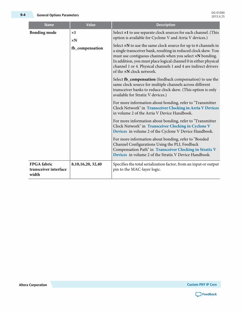
DescriptionValueName
Select ×1 to use separate clock sources for each channel. (Thisoption is available for Cyclone V and Arria V devices.)
Select ×N to use the same clock source for up to 6 channels ina single transceiver bank, resulting in reduced clock skew. Youmust use contiguous channels when you select ×N bonding.In addition, you must place logical channel 0 in either physicalchannel 1 or 4. Physical channels 1 and 4 are indirect driversof the ×N clock network.
Select fb_compensation (feedback compensation) to use thesame clock source for multiple channels across differenttransceiver banks to reduce clock skew. (This option is onlyavailable for Stratix V devices.)
For more information about bonding, refer to "TransmitterClock Network" in Transceiver Clocking inArria VDevicesin volume 2 of the Arria V Device Handbook.
For more information about bonding, refer to "TransmitterClock Network" in Transceiver Clocking in Cyclone VDevices in volume 2 of the Cyclone V Device Handbook.
For more information about bonding, refer to "BondedChannel Configurations Using the PLL FeedbackCompensation Path" in Transceiver Clocking in Stratix VDevices in volume 2 of the Stratix V Device Handbook.
×1
×N
fb_compensation
Bonding mode
Specifies the total serialization factor, from an input or outputpin to the MAC-layer logic.
8,10,16,20, 32,40FPGA fabrictransceiver interfacewidth
Custom PHY IP CoreAltera Corporation
Feedback
UG-01080General Options Parameters9-4 2013.4.25

DescriptionValueName
The PCS-PMA interface width depends on the FPGA fabrictransceiver interface width and whether 8B/10B is enabled.The following combinations are available:
PMA InterfaceWidth
8B/10BFPGA/XCVR
8No8
10Yes8
10No10
8 or 16No16
10 or 20Yes16
10 or20No20
16No32
20Yes32
20No40
8, 10, 16, 20PCS-PMA interfacewidth
The CMU PLL is available for Arria V and Cyclone V devices.
For Stratix V devices, you can select either the CMU or ATXPLL. TheCMUPLLhas a larger frequency range than theATXPLL. The ATX PLL is designed to improve jitter performanceand achieves lower channel-to-channel skew; however, itsupports a narrower range of data rates and reference clockfrequencies. Another advantage of theATX PLL is that it doesnot use a transceiver channel, while the CMU PLL does.
Because the CMU PLL is more versatile, it is specified as thedefault setting. An informational message displays in themessage pane telling you whether the chosen settings for Datarate and Input clock frequency are legal for the CMU PLL, orfor both the CMU and ATX PLLs.
CMU ATXPLL type
Specifies the data rate. The possible data rates depend uponthe device and configuration specified.
622-11000 MbpsData rate
The base data rate is the frequency of the clock input to thePLL. Select a base data rate that minimizes the number ofPLLs required to generate all the clocks required for datatransmission. By selecting an appropriate base data rate, youcan change data rates by changing the divider used by the clockgeneration block. For higher frequency data rates 2 × and 4×base data rates are not available.
1 × Data rate
2 × Data rate
4 × Data rate
Base data rate
Specifies the frequency of the PLL input reference clock.VariableInput clock frequency
Altera CorporationCustom PHY IP Core
Feedback
9-5General Options ParametersUG-010802013.4.25
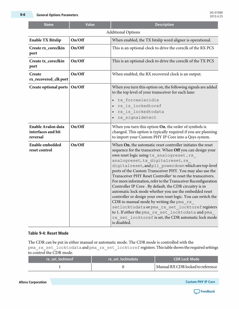
DescriptionValueName
Additional Options
When enabled, the TX bitslip word aligner is operational.On/OffEnable TX Bitslip
This is an optional clock to drive the coreclk of the RX PCSOn/OffCreate rx_coreclkinport
This is an optional clock to drive the coreclk of the TX PCSOn/OffCreate tx_coreclkinport
When enabled, the RX recovered clock is an output.On/OffCreaterx_recovered_clk port
When you turn this option on, the following signals are addedto the top level of your transceiver for each lane:
• tx_forceelecidle• rx_is_lockedtoref• rx_is_lockedtodata• rx_signaldetect
On/OffCreate optional ports
When you turn this option On, the order of symbols ischanged. This option is typically required if you are planningto import your Custom PHY IP Core into a Qsys system.
On/OffEnable Avalon datainterfaces and bitreversal
When On, the automatic reset controller initiates the resetsequence for the transceiver. When Off you can design yourown reset logic using tx_analogreset , rx_analogreset, tx_digitalreset, rx_digitalreset, andpll_powerdownwhich are top-levelports of the Custom Transceiver PHY. You may also use theTransceiver PHY Reset Controller' to reset the transceivers.Formore information, refer to theTransceiver ReconfigurationController IP Core . By default, the CDR circuitry is inautomatic lock mode whether you use the embedded resetcontroller or design your own reset logic. You can switch theCDR to manual mode by writing the pma_rx_setlocktodata orpma_rx_set_locktoref registersto 1. If either the pma_rx_set_locktodata and pma_rx_set_locktoref is set, the CDR automatic lock modeis disabled.
On/OffEnable embeddedreset control
Table 9-4: Reset Mode
The CDR can be put in either manual or automatic mode. The CDR mode is controlled with thepma_rx_set_locktodata andpma_rx_set_locktoref registers. This table shows the required settingsto control the CDR mode.
CDR Lock Moderx_set_locktodatarx_set_locktoref
Manual RXCDR locked to reference01
Custom PHY IP CoreAltera Corporation
Feedback
UG-01080General Options Parameters9-6 2013.4.25

CDR Lock Moderx_set_locktodatarx_set_locktoref
Manual RX CDR locked to data1X
Automatic RX CDR00
Related InformationTransceiver Reset Control in Stratix V Devices
Word Alignment ParametersThe word aligner restores word boundaries of received data based on a predefined alignment pattern. Thispattern can be 7, 8, 10, 16, 20, or 32 bits long. The word alignment module searches for a programmedpattern to identify the correct boundary for the incoming stream.
Altera CorporationCustom PHY IP Core
Feedback
9-7Word Alignment ParametersUG-010802013.4.25
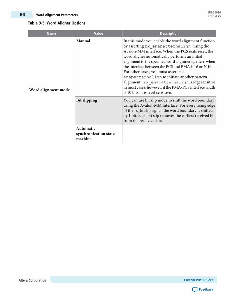
Table 9-5: Word Aligner Options
DescriptionValueName
In this mode you enable the word alignment functionby asserting rx_enapatternalign using theAvalon-MM interface. When the PCS exits reset, theword aligner automatically performs an initialalignment to the specifiedword alignment patternwhenthe interface between the PCS and PMA is 16 or 20 bits.For other cases, you must assert rx_enapatternalign to initiate another patternalignment. rx_enapatternalign is edge sensitiveinmost cases; however, if the PMA-PCS interfacewidthis 10 bits, it is level sensitive.
Manual
Word alignment mode
You can use bit slip mode to shift the word boundaryusing the Avalon-MM interface. For every rising edgeof the rx_bitslip signal, the word boundary is shiftedby 1 bit. Each bit slip removes the earliest received bitfrom the received data.
Bit slipping
Automaticsynchronization statemachine
Custom PHY IP CoreAltera Corporation
Feedback
UG-01080Word Alignment Parameters9-8 2013.4.25
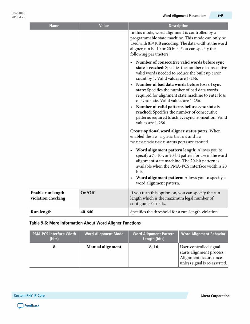
DescriptionValueName
In this mode, word alignment is controlled by aprogrammable state machine. This mode can only beusedwith 8B/10B encoding. The datawidth at thewordaligner can be 10 or 20 bits. You can specify thefollowing parameters:
• Number of consecutive valid words before syncstate is reached: Specifies the number of consecutivevalid words needed to reduce the built up errorcount by 1. Valid values are 1-256.
• Number of bad data words before loss of syncstate: Specifies the number of bad data wordsrequired for alignment state machine to enter lossof sync state. Valid values are 1-256.
• Number of valid patterns before sync state isreached: Specifies the number of consecutivepatterns required to achieve synchronization. Validvalues are 1-256.
Create optional word aligner status ports: Whenenabled the rx_syncstatus and rx_patterndetect status ports are created.
• Word alignment pattern length: Allows you tospecify a 7-, 10-, or 20-bit pattern for use in thewordalignment state machine. The 20-bit pattern isavailable when the PMA-PCS interface width is 20bits.
• Word alignment pattern: Allows you to specify aword alignment pattern.
If you turn this option on, you can specify the runlength which is the maximum legal number ofcontiguous 0s or 1s.
On/OffEnable run lengthviolation checking
Specifies the threshold for a run-length violation.40-640Run length
Table 9-6: More Information About Word Aligner Functions
Word Alignment BehaviorWord Alignment PatternLength (bits)
Word Alignment ModePMA-PCS Interface Width(bits)
User-controlled signalstarts alignment process.Alignment occurs onceunless signal is re-asserted.
8, 16Manual alignment8
Altera CorporationCustom PHY IP Core
Feedback
9-9Word Alignment ParametersUG-010802013.4.25

Word Alignment BehaviorWord Alignment PatternLength (bits)
Word Alignment ModePMA-PCS Interface Width(bits)
User-controlled signalstarts alignment process.Alignment occurs onceunless signal is re-asserted.
7 , 10
Manual alignment
10Data must be 8B/10Bencoded and aligns toselected word alignerpattern.
Automatic synchronizedstate machine
User-controlled signalstarts alignment process.Alignment occurs onceunless signal is re-asserted.
8 , 16, 32Manual alignment16
User-controlled signalstarts alignment process.Alignment occurs onceunless signal is re-asserted.
8 , 16, 32Manual alignment
20Automatically selectedword aligner patternlength and pattern.
7, 10, or 20 bitsAutomatic SynchronizedState Machine
Related InformationTransceiver Architecture in Stratix V Devices
Transceiver Architecture in Arria V Devices
Transceiver Architecture in Cyclone V Devices
Rate Match FIFO ParametersThe rate match FIFO compensates for small clock frequency differences between the upstream transmitterand the local receiver clocks by inserting or removing skip (SKP) symbols or ordered-sets from the inter-packetgap (IPG) or idle streams. It deletes SKP symbols or ordered-sets when the upstream transmitter referenceclock frequency is greater than the local receiver reference clock frequency. It inserts SKP symbols orordered-sets when the local receiver reference clock frequency is greater than the upstream transmitterreference clock frequency.
If you enable the rate match FIFO, the MegaWizard Plug-In Manager provides options to enter the ratematch insertion and deletion patterns. The lower 10 bits are the control pattern, and the upper 10 bits arethe skip pattern.
Custom PHY IP CoreAltera Corporation
Feedback
UG-01080Rate Match FIFO Parameters9-10 2013.4.25

Table 9-7: Rate Match FIFO Options
DescriptionValueName
Turn this option on, to enable therate match functionality. Turningthis option on adds the rx_rmfifodatainserted, andrx_rmfifodatadeleted statussignals to your PHY.
On/OffEnable rate match FIFO
Enter a 10-bit skip pattern (bits10-19) and a 10-bit control pattern(bits 0-9). The skip pattern musthave neutral disparity.
1101000011
1010000011
Ratematch insertion/deletion +vedisparity pattern
Enter a 10-bit skip pattern (bits10-19) and a 10-bit control pattern(bits 0-9). The skip pattern musthave neutral disparity.
0010111100
0101111100
Rate match insertion/deletion -vedisparity pattern
When enabled, creates the rx_rmfifoddatainserted andrx_rmfifodatadeletedsignals from the rate match FIFObecome output ports.
On/OffCreate optional rate match FIFOstatus ports
8B/10B Encoder and Decoder ParametersThe 8B/10B encoder generates 10-bit code groups (control or data word) with proper disparity from the8-bit data and 1-bit control identifier. The 8B/10B decoder receives 10-bit data from the rate matcher anddecodes it into an 8-bit data and 1-bit control identifier.
Table 9-8: 8B/10B Options
DescriptionValueName
Enable this option if yourapplication requires 8B/10Bencoding and decoding. This optionon adds the tx_datak <n>, rx_datak <n>, and rx_runningdisp <n> signals toyour transceiver.
On/OffEnable 8B/10B decoder/encoder
When enabled, you can use thetx_forcedisp signal to control thedisparity of the 8B/10B encoder.Turning this option on adds thetx_forcedisp and tx_dispvalsignals to your transceiver.
On/OffEnable manual disparity control
Altera CorporationCustom PHY IP Core
Feedback
9-118B/10B Encoder and Decoder ParametersUG-010802013.4.25
DescriptionValueName
Enable this option to include the8B/10B rx_errdetect and rx_disperr error signals at the toplevel of the Custom PHY IP Core.
On/OffCreate optional 8B/10B status port
Byte Order ParametersThe byte ordering block is available when the PCS width is doubled at the byte deserializer. Byte orderingidentifies the first byte of a packet by determining whether the programmed start-of-packet (SOP) patternis present; it inserts enough pad characters in the data stream to force the SOP to the lowest order byte lane.
You cannot enable Rate Match FIFO when your application requires byte ordering. Because the ratematch function inserts and deletes idle characters, it may shift the SOP to a different byte lane.
Note:
Custom PHY IP CoreAltera Corporation
Feedback
UG-01080Byte Order Parameters9-12 2013.4.25
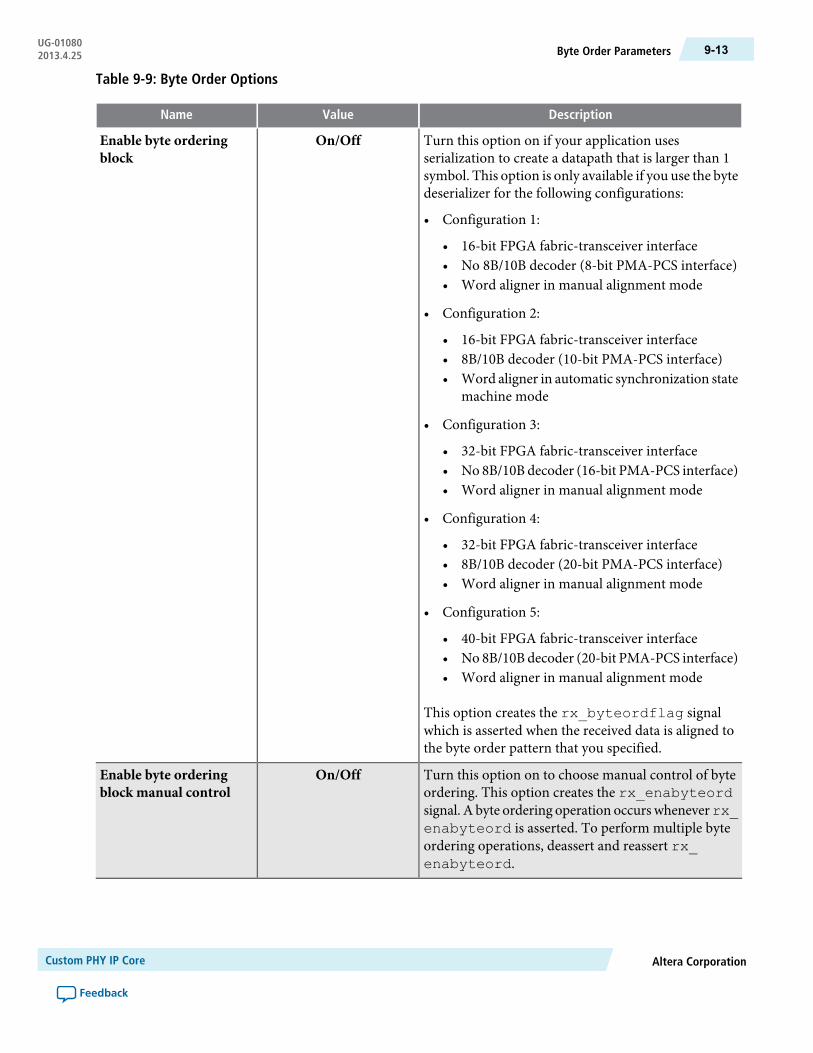
Table 9-9: Byte Order Options
DescriptionValueName
Turn this option on if your application usesserialization to create a datapath that is larger than 1symbol. This option is only available if you use the bytedeserializer for the following configurations:
• Configuration 1:
• 16-bit FPGA fabric-transceiver interface• No 8B/10B decoder (8-bit PMA-PCS interface)• Word aligner in manual alignment mode
• Configuration 2:
• 16-bit FPGA fabric-transceiver interface• 8B/10B decoder (10-bit PMA-PCS interface)• Word aligner in automatic synchronization state
machine mode
• Configuration 3:
• 32-bit FPGA fabric-transceiver interface• No8B/10B decoder (16-bit PMA-PCS interface)• Word aligner in manual alignment mode
• Configuration 4:
• 32-bit FPGA fabric-transceiver interface• 8B/10B decoder (20-bit PMA-PCS interface)• Word aligner in manual alignment mode
• Configuration 5:
• 40-bit FPGA fabric-transceiver interface• No8B/10B decoder (20-bit PMA-PCS interface)• Word aligner in manual alignment mode
This option creates the rx_byteordflag signalwhich is asserted when the received data is aligned tothe byte order pattern that you specified.
On/OffEnable byte orderingblock
Turn this option on to choose manual control of byteordering. This option creates the rx_enabyteordsignal. A byte ordering operation occurswheneverrx_enabyteord is asserted. To perform multiple byteordering operations, deassert and reassert rx_enabyteord.
On/OffEnable byte orderingblock manual control
Altera CorporationCustom PHY IP Core
Feedback
9-13Byte Order ParametersUG-010802013.4.25

DescriptionValueName
Specifies the pattern that identifies the SOP. For 16-bitbyte ordering pattern you must include a 2-bit pad sothat the pattern entered is in the following format: 00<pattern> 00 <pattern>. For example, if the requiredpattern is 10111100, enter the following pattern:00101111000010111100
Enter the byte ordering pattern as follows based on the5 configurations that support byte ordering as describedin the Enable byte ordering block:
• Configuration 1: 8-bits• Configuration 2: 10-bits
For example: If you select a /Kx.y/ control codegroup as the byte ordering pattern, the mostsignificant 2 bits of the 10-bit byte ordering patternmust be 2'b01. If you select a /Dx.y/ data code groupas the byte ordering pattern, the most significant2-bits of the 10-bit byte ordering pattern must be2'b00. The least significant 8-bitsmust be the 8B/10Bdecoded version of the code group used for byteordering.
• Configuration 3:16-bits, 8-bits• Configuration 4: 20-bits only
For example: If you select a /Kx.y/Dx.y/ code groupas the byte ordering pattern, the most significant2-bits of the 20-bit byte ordering pattern must be2'b01. Similarly bit[9:0] must be 2'b00. Bit[18:10]must be the 8B/10B decoded version of /Kx.y/.Bit[7:0] must be 8B/10B decoded version of /Dx.y/.
• Configuration 5: 20-bits, 10-bits
Depends onconfiguration
Byte ordering pattern
Specifies the pad pattern that is inserted to align theSOP. Enter the following size pad patterns:
Pad Pattern8B/10B En-coded?
Data Width
No8, 16, 32
10 bitsNo10,20,40
9 bitsNo8, 16, 3
00000000Byte orderingpadpattern
Custom PHY IP CoreAltera Corporation
Feedback
UG-01080Byte Order Parameters9-14 2013.4.25
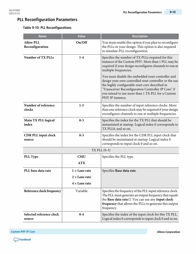
PLL Reconfiguration Parameters
Table 9-10: PLL Reconfigurations
DescriptionValueName
You must enable this option if you plan to reconfigurethe PLLs in your design. This option is also requiredto simulate PLL reconfiguration.
On/OffAllow PLLReconfiguration
Specifies the number of TX PLLs required for thisinstance of the Custom PHY. More than 1 PLL may berequired if your design reconfigures channels to run atmultiple frequencies.
You must disable the embedded reset controller anddesign your own controlled reset controller or the usethe highly configurable reset core described in"Transceiver Reconfiguration Controller IP Core" ifyou intend to use more than 1 TX PLL for a CustomPHY IP instance.
1-4Number of TX PLLs
Specifies the number of input reference clocks. Morethan one reference clockmay be required if your designreconfigures channels to run at multiple frequencies.
1-5Number of referenceclocks
Specifies the index for the TX PLL that should beinstantiated at startup. Logical index 0 corresponds toTX PLL0, and so on.
0-3Main TX PLL logicalindex
Specifies the index for the CDR PLL input clock thatshould be instantiated at startup. Logical index 0corresponds to input clock 0 and so on.
0-3CDR PLL input clocksource
TX PLL (0-3)
Specifies the PLL type.CMU
ATX
PLL Type
Specifies Base data rate.1 × Lane rate
2 × Lane rate
4 × Lane rate
PLL base data rate
Specifies the frequency of the PLL input reference clock.The PLLmust generate an output frequency that equalsthe Base data rate/2. You can use any Input clockfrequency that allows the PLLs to generate this outputfrequency.
VariableReference clock frequency
Specifies the index of the input clock for this TX PLL.Logical index 0 corresponds to input clock 0 and so on.
0-4Selected reference clocksource
Altera CorporationCustom PHY IP Core
Feedback
9-15PLL Reconfiguration ParametersUG-010802013.4.25
DescriptionValueName
Channel Interface
Turn this option on to enable PLL and datapathdynamic reconfiguration.When you select this option,the width of tx_parallel_data and rx_parallel_data buses increases in the followingway.
• n The tx_parallel_data bus is 44 bits perlane; however, only the low-order number of bitsspecified by the FPGA fabric transceiver interfacewidth contain valid data for each lane.
• n The rx_parallel_data bus is 64 bits perlane; however, only the low-order number of bitsspecified by the FPGA fabric transceiver interfacewidth contain valid data.
On/OffEnable channel interface
Related InformationGeneral Options Parameters on page 9-3
Analog ParametersClick the appropriate link to specify the analog options for your device:
Related InformationAnalog Settings for Arria V Devices on page 19-2
Analog Settings for Arria V GZ Devices on page 19-9
Analog Settings for Cyclone V Devices on page 19-18
Analog Settings for Stratix V Devices on page 19-25
Presets for EthernetPresets allow you to specify a group of parameters to implement a particular protocol or application. If youapply the presets for GIGE-1.25 Gbps or GIGE–2.5 Gbps, parameters with specific required values for thoseprotocols are set for you. Selecting a preset does not prevent you from changing any parameter to meet therequirements of your design.
Table 9-11: Presets for Ethernet Protocol
GIGE-2.50 GbpsGIGE-1.25 GbpsParameter Name
General Options Tab
GIGEGIGEParameter validation rules
OffOffEnable bonding
168FPGA fabric transceiver interfacewidth
Custom PHY IP CoreAltera Corporation
Feedback
UG-01080Analog Parameters9-16 2013.4.25
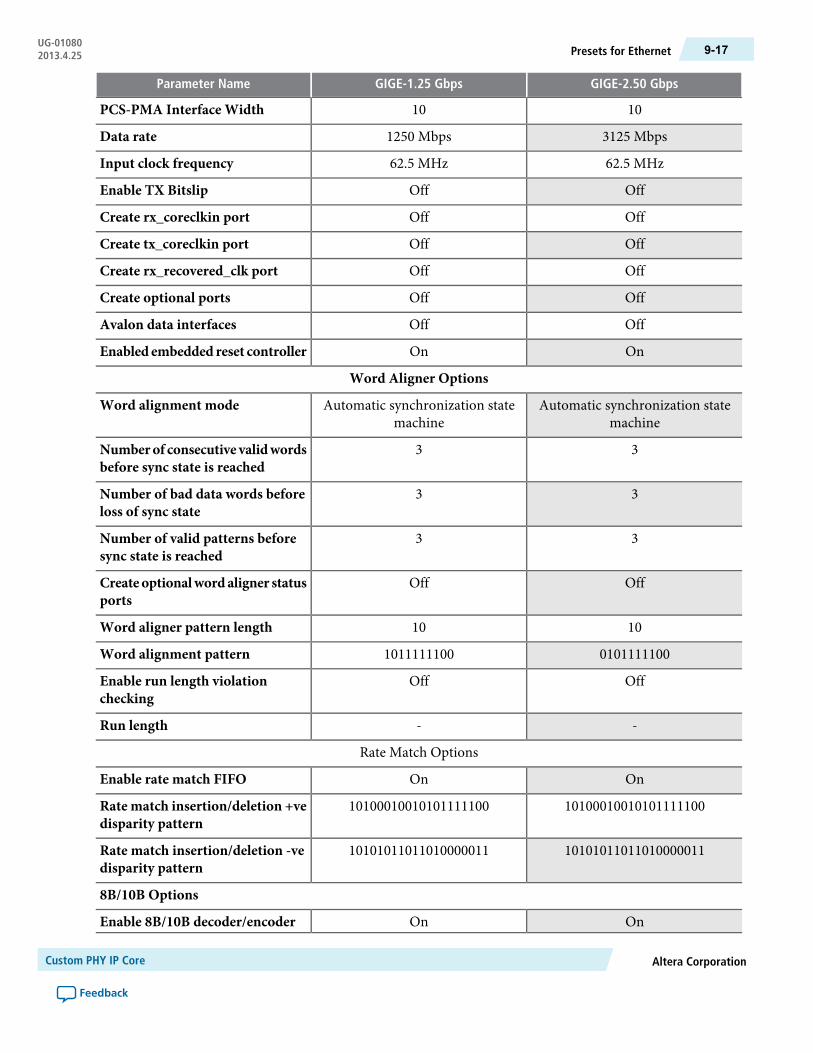
GIGE-2.50 GbpsGIGE-1.25 GbpsParameter Name
1010PCS-PMA Interface Width
3125 Mbps1250 MbpsData rate
62.5 MHz62.5 MHzInput clock frequency
OffOffEnable TX Bitslip
OffOffCreate rx_coreclkin port
OffOffCreate tx_coreclkin port
OffOffCreate rx_recovered_clk port
OffOffCreate optional ports
OffOffAvalon data interfaces
OnOnEnabled embedded reset controller
Word Aligner Options
Automatic synchronization statemachine
Automatic synchronization statemachine
Word alignment mode
33Numberof consecutive validwordsbefore sync state is reached
33Number of bad data words beforeloss of sync state
33Number of valid patterns beforesync state is reached
OffOffCreate optionalwordaligner statusports
1010Word aligner pattern length
01011111001011111100Word alignment pattern
OffOffEnable run length violationchecking
--Run length
Rate Match Options
OnOnEnable rate match FIFO
1010001001010111110010100010010101111100Ratematch insertion/deletion +vedisparity pattern
1010101101101000001110101011011010000011Rate match insertion/deletion -vedisparity pattern
8B/10B Options
OnOnEnable 8B/10B decoder/encoder
Altera CorporationCustom PHY IP Core
Feedback
9-17Presets for EthernetUG-010802013.4.25

GIGE-2.50 GbpsGIGE-1.25 GbpsParameter Name
OffOffEnable manual disparity control
OffOffCreate optional 8B/10B status port
Byte Order Options
OffOffEnable byte ordering block
OffOffEnable byte orderingblockmanualcontrol
--Byte ordering pattern
--Byte ordering pad pattern
InterfacesFigure 9-2: Custom PHY Top-Level Signals
The variables in Figure 9–2 represent the following parameters:
• <n>—The number of lanes• <w>—The width of the FPGA fabric to transceiver interface per lane• <s>— The symbol size• <p>—The number of PLLs
Figure 9-3: Custom PHY Interfaces
tx_parallel_data[<n><w>-1>:0]tx_clkouttx_datak[<n>(<w>/<s>)-1:0]tx_forcedisp[<n>(<w>/<s>)-1:0]tx_dispval[<n>(<w>/<s>)-1:0]
rx_parallel_data[<n><w>-1:0]rx_clkout[<n>-1:0]rx_datak[<n>(<w>/<s>)-1:0]rx_runningdisp[<n>(<w>/<s>)-1:0]rx_enabyteord[<n>-1:0]
phy_mgmt_clkphy_mgmt_clk_resetphy_mgmt_address[8:0]phy_mgmt_writedata[31:0]phy_mgmt_readdata[31:0]phy_mgmt_writephy_mgmt_readphy_mgmt_waitrequest
pll_ref_clkrx_coreclkin[<n>-1:0]tx_coreclkin[<n>-1:0]
Custom PHY Top-Level Signals
tx_serial_data[<n>-1:0]rx_serial_data[<n>-1:0]
tx_readyrx_ready
pll_locked[<p>-1:0]tx_forceelecidle[<n>-1:0]
tx_bitslipboundaryselect[<n>5-1:0]rx_disperr[<n>(<w>/<s>)-1:0]
rx_errdetect[<n>(<w>/<s>)-1:0]rx_syncstatus[<n>(<w>/<s>)-1:0]
rx_is_lockedtoref[<n>-1:0]rx_is_lockedtodata[<n>-1:0]
rx_signaldetect[<n>-1:0]rx_bitslip[<n>-1:0]
rx_bitslipboundaryselectout[<n>5-1:0]rx_patterndetect[<n>(<w>/<s>)-1:0]
rx_rmfifodatainserted[<n>-1:0]rx_rmfifodatadeleted[<n>-1:0]
rx_rlv[<n>-1:0]rx_recovered_clk[<n>-1:0]
rx_byteordflag[<n>-1:0]
pll_powerdowntx_digitalreset[<n>-1:0]tx_analogreset[<n>-1:0]
tx_cal_busy[<n>-1:0]rx_digitalreset[<n>-1:0]rx_analogreset[<n>-1:0]
rx_cal_busy[<n>-1:0]
reconfig_to_xcvr[(<n>70-1):0]reconfig_from_xcvr[(<n>46-1):0]
Avalon-ST Txfrom MAC
SpeedSerial I/O
Avalon-MM PHYManagementInterface
Clocks Optional
Optional
Status(Optional)
Avalon-ST Rxto MAC
TransceiverReconfiguration
Interface
Optional
Reset Controland Status(Optional)
Custom PHY IP CoreAltera Corporation
Feedback
UG-01080Interfaces9-18 2013.4.25

By default block diagram shown in the MegaWizard Plug-In Manager labels the external pins withthe interface type and places the interface name inside the box. The interface type and name are used
Note:
in the _hw.tcl file that describes the component. If you turn on Show signals, the block diagramdisplays all top-level signal names.
Related InformationComponent Interface Tcl Reference
Data InterfacesThis topic describes the Avalon-ST TX and RX interface signals as well as the serial interface and statussignals.
Table 9-12: Avalon-ST TX Interface Signals
DescriptionDirectionSignal Name
This is TX parallel data driven from the MAC. The readylatency on this interface is 0, so that the PHY must be able toaccept data as soon as it comes out of reset.
Inputtx_parallel_data[( <n><w>)-1:0]
This is the clock for TX parallel data, control, and statussignals.
Outputtx_clkout
Data and control indicator for the received data. When 0,indicates that tx_data is data, when 1, indicates that tx_datais control.
Inputtx_datak[< n >(<w>/<s>)-1:0]
When asserted, this control signal enables disparity to beforced on the TX channel. This signal is created if you turnOn the Enable manual disparity control option on the8B/10B tab.
Inputtx_forcedisp[< n >(<w>/<s>)-1:0]
This control signal specifies the disparity of the data. This portis created if you turn On the Enable disparity control optionon the 8B/10B tab.
Inputtx_dispval[< n >(<w>/<s>)-1:0]
Table 9-13: Avalon-ST RX Interface Signals
These signals are driven from the PCS to the MAC. This is an Avalon source interface.DescriptionDirectionSignal Name
This is RX parallel data driven from theCustomPHY IPCore.The ready latency on this interface is 0, so that the MAC mustbe able to accept data as soon as the PHY comes out of reset.Data driven from this interface is always valid.
Outputrx_parallel_data[< n><w>-1:0]
This is the clock for the RX parallel data source interface.Outputrx_clkout[< n >-1:0]
Data and control indicator for the source data. When 0,indicates that rx_parallel_data is data, when 1,indicates that rx_parallel_data is control.
Outputrx_datak[< n >(<w>/<s>)-1:0]
Altera CorporationCustom PHY IP Core
Feedback
9-19Data InterfacesUG-010802013.4.25
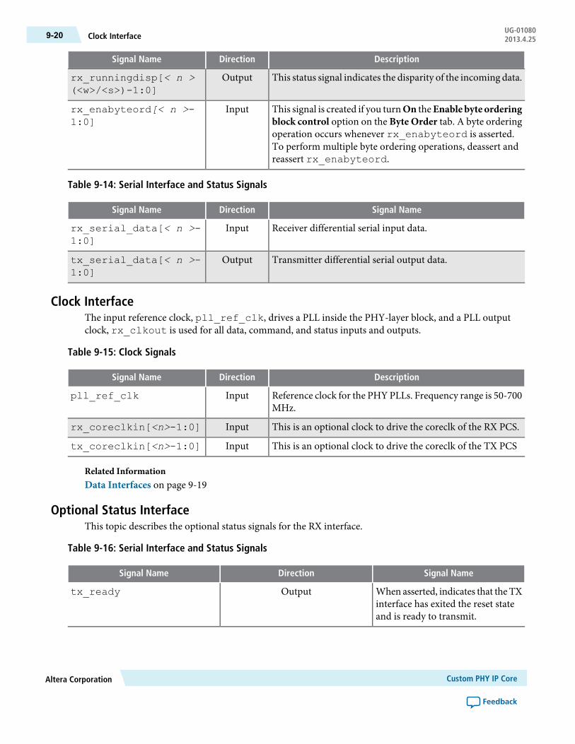
DescriptionDirectionSignal Name
This status signal indicates the disparity of the incoming data.Outputrx_runningdisp[< n >(<w>/<s>)-1:0]
This signal is created if you turnOn theEnable byte orderingblock control option on the Byte Order tab. A byte orderingoperation occurs whenever rx_enabyteord is asserted.To perform multiple byte ordering operations, deassert andreassert rx_enabyteord.
Inputrx_enabyteord[< n >-1:0]
Table 9-14: Serial Interface and Status Signals
Signal NameDirectionSignal Name
Receiver differential serial input data.Inputrx_serial_data[< n >-1:0]
Transmitter differential serial output data.Outputtx_serial_data[< n >-1:0]
Clock InterfaceThe input reference clock, pll_ref_clk, drives a PLL inside the PHY-layer block, and a PLL outputclock, rx_clkout is used for all data, command, and status inputs and outputs.
Table 9-15: Clock Signals
DescriptionDirectionSignal Name
Reference clock for the PHY PLLs. Frequency range is 50-700MHz.
Inputpll_ref_clk
This is an optional clock to drive the coreclk of the RX PCS.Inputrx_coreclkin[<n>-1:0]
This is an optional clock to drive the coreclk of the TX PCSInputtx_coreclkin[<n>-1:0]
Related InformationData Interfaces on page 9-19
Optional Status InterfaceThis topic describes the optional status signals for the RX interface.
Table 9-16: Serial Interface and Status Signals
Signal NameDirectionSignal Name
When asserted, indicates that theTXinterface has exited the reset stateand is ready to transmit.
Outputtx_ready
Custom PHY IP CoreAltera Corporation
Feedback
UG-01080Clock Interface9-20 2013.4.25

Signal NameDirectionSignal Name
When asserted, indicates that theRXinterface has exited the reset stateand is ready to receive.
Outputrx_ready
When asserted, indicates that thePLL is locked to the input referenceclock.
Outputpll_locked[<p>-1:0]
When asserted, enables a circuit todetect a downstream receiver. It isused for the PCI Express protocol.This signalmust be driven lowwhennot in use because it causes the TXPMA to enter electrical idle modeand tristate the TX serial datasignals.
Inputtx_forceelecidle[<n>-1:0]
When asserted, indicates that thePLL is locked to the input referenceclock.
Inputtx_bitslipboundaryselect[<n>5-1:0]
When asserted, indicates that thereceived 10-bit code or data grouphas a disparity error.
Outputrx_disperr[<n>(<w>/<s>)-1:0]
When asserted, indicates that areceived 10-bit code group has an8B/10B code violation or disparityerror.
Outputrx_errdetect[<n>(<w>/<s>)-1:0]
Indicates presence or absence ofsynchronization on theRX interface.Asserted when word aligneridentifies the word alignmentpattern or synchronization codegroups in the received data stream.This signal is optional.
Outputrx_syncstatus[ <n> (<w>/<s>)-1:0]
Asserted when the receiver CDR islocked to the input reference clock.This signal is asynchronous. Thissignal is optional.
Outputrx_is_lockedtoref[ <n> -1:0]
When asserted, the receiver CDR isin to lock-to-data mode. Whendeasserted, the receiver CDR lockmode depends on the rx_locktorefclk signal level. Thissignal is optional.
Outputrx_is_lockedtodata[ <n>-1:0]
Altera CorporationCustom PHY IP Core
Feedback
9-21Optional Status InterfaceUG-010802013.4.25

Signal NameDirectionSignal Name
Signal threshold detect indicatorrequired for the PCI Expressprotocol.When asserted, it indicatesthat the signal present at the receiverinput buffer is above theprogrammed signal detectionthreshold value.
Outputrx_signaldetect[ <n> -1:0]
Used for manual control of bitslipping. The word aligner slips a bitof the current word for every risingedge of this signal.
Inputrx_bitslip[ <n> -1:0]
This signal is used for bit slip wordalignment mode. It reports thenumber of bits that the RX blockslipped to achieve a deterministiclatency.
Outputrx_bitslipboundaryselectout[ <n> 5-1:0]
When asserted, indicates that theprogrammed word alignmentpattern has been detected in thecurrent word boundary.
Outputrx_patterndetect[<n>(<w>/<s>)-1:0]
When asserted, indicates that theRXrate match block inserted an ||R||column.
Outputrx_rmfifodatainserted[<n>-1:0]
When asserted, indicates that theRXrate match block deleted an ||R||column.
Outputrx_rmfifodatadeleted[<n>-1:0]
When asserted, indicates a runlength violation. Asserted if thenumber of consecutive 1s or 0sexceeds the number specified in theMegaWizard Plug-In Manager.
Outputrx_rlv[ <n> -1:0]
This is the RX clock which isrecovered from the received datastream.
Outputrx_recovered_clk[<n>-1:0]
This status flag is asserted high thereceived data is aligned to the byteorder pattern that you specify.
Outputrx_byteordflag[<n>-1:0]
Optional Reset Control and Status InterfaceThis topic describes the signals in the optional reset control and status interface. These signals are availableif you do not enable the embedded reset controller.
Custom PHY IP CoreAltera Corporation
Feedback
UG-01080Optional Reset Control and Status Interface9-22 2013.4.25
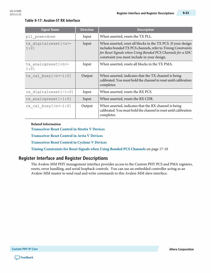
Table 9-17: Avalon-ST RX Interface
DescriptionDirectionSignal Name
When asserted, resets the TX PLL.Inputpll_powerdown
When asserted, reset all blocks in the TX PCS. If your designincludes bondedTXPCS channels, refer toTimingConstraintsfor Reset Signals when Using Bonded PCS Channels for a SDCconstraint you must include in your design.
Inputtx_digitalreset[<n>-1:0]
When asserted, resets all blocks in the TX PMA.Inputtx_analogreset[<n>-1:0]
When asserted, indicates that the TX channel is beingcalibrated. Youmust hold the channel in reset until calibrationcompletes.
Outputtx_cal_busy[<n>-1:0]
When asserted, resets the RX PCS.Inputrx_digitalreset[-1:0]
When asserted, resets the RX CDR.Inputrx_analogreset[-1:0]
When asserted, indicates that the RX channel is beingcalibrated. Youmust hold the channel in reset until calibrationcompletes.
Outputrx_cal_busy[<n>-1:0]
Related InformationTransceiver Reset Control in Stratix V Devices
Transceiver Reset Control in Arria V Devices
Transceiver Reset Control in Cyclone V Devices
Timing Constraints for Reset Signals when Using Bonded PCS Channels on page 17-10
Register Interface and Register DescriptionsThe Avalon-MM PHY management interface provides access to the Custom PHY PCS and PMA registers,resets, error handling, and serial loopback controls. You can use an embedded controller acting as anAvalon-MM master to send read and write commands to this Avalon-MM slave interface.
Altera CorporationCustom PHY IP Core
Feedback
9-23Register Interface and Register DescriptionsUG-010802013.4.25

Figure 9-4: Custom PHY IP Core
Table 9-18: Avalon-MM PHY Management Interface
DescriptionDirectionSignal Name
Avalon-MM clock input. There isno frequency restriction for thephy_mgmt_clk; however, if youplan to use the same clock for thePHY management interface andtransceiver reconfiguration, youmust restrict the frequency range ofphy_mgmt_clk to 100-150 MHzto meet the specification for thetransceiver reconfiguration clock.
Inputphy_mgmt_clk
Global reset signal. This signal isactive high and level sensitive.
Inputphy_mgmt_clk_reset
9-bit Avalon-MM address.Inputphy_mgmt_address[8:0]
Input data.Inputphy_mgmt_writedata[31:0]
Output data.Outputphy_mgmt_readdata[31:0]
Write signal.Inputphy_mgmt_write
Read signal.Inputphy_mgmt_read
When asserted, indicates that theAvalon-MMslave interface is unableto respond to a read orwrite request.When asserted, control signals totheAvalon-MMslave interfacemustremain constant.
Outputphy_mgmt_waitrequest
Custom PHY IP Core RegistersThis topic specifies the registers that you can access over the PHYmanagement interface usingword addressesand a 32-bit embedded processor. A single address space provides access to all registers.
Writing to reserved or undefined register addresses may have undefined side effects.Note:
Custom PHY IP CoreAltera Corporation
Feedback
UG-01080Custom PHY IP Core Registers9-24 2013.4.25
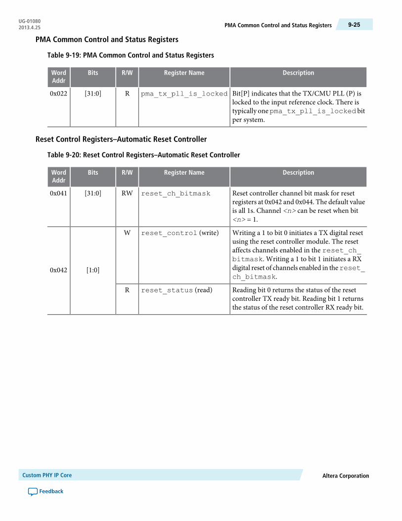
PMA Common Control and Status Registers
Table 9-19: PMA Common Control and Status Registers
DescriptionRegister NameR/WBitsWordAddr
Bit[P] indicates that the TX/CMU PLL (P) islocked to the input reference clock. There istypically onepma_tx_pll_is_locked bitper system.
pma_tx_pll_is_lockedR[31:0]0x022
Reset Control Registers–Automatic Reset Controller
Table 9-20: Reset Control Registers–Automatic Reset Controller
DescriptionRegister NameR/WBitsWordAddr
Reset controller channel bit mask for resetregisters at 0x042 and 0x044. The default valueis all 1s. Channel <n> can be reset when bit<n> = 1.
reset_ch_bitmaskRW[31:0]0x041
Writing a 1 to bit 0 initiates a TX digital resetusing the reset controller module. The resetaffects channels enabled in the reset_ch_bitmask. Writing a 1 to bit 1 initiates a RXdigital reset of channels enabled in thereset_ch_bitmask.
reset_control (write)W
[1:0]0x042
Reading bit 0 returns the status of the resetcontroller TX ready bit. Reading bit 1 returnsthe status of the reset controller RX ready bit.
reset_status (read)R
Altera CorporationCustom PHY IP Core
Feedback
9-25PMA Common Control and Status RegistersUG-010802013.4.25
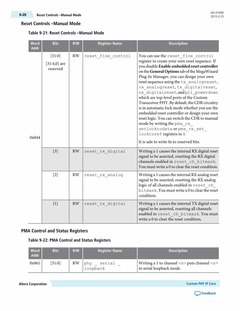
Reset Controls –Manual Mode
Table 9-21: Reset Controls –Manual Mode
DescriptionRegister NameR/WBitsWordAddr
You can use the reset_fine_controlregister to create your own reset sequence. Ifyou disableEnable embedded reset controlleron theGeneralOptions tab of theMegaWizardPlug-In Manager, you can design your ownreset sequence using the tx_analogreset,rx_analogreset, tx_digitalreset,rx_digitalreset, andpll_powerdownwhich are top-level ports of the CustomTransceiver PHY. By default, theCDR circuitryis in automatic lock mode whether you use theembedded reset controller or design your ownreset logic. You can switch the CDR to manualmode by writing the pma_rx_setlocktodata or pma_rx_set_locktoref registers to 1.
It is safe to write 0s to reserved bits.
reset_fine_controlRW[31:0]
[31:4,0] arereserved
0x044
Writing a 1 causes the internal RX digital resetsignal to be asserted, resetting the RX digitalchannels enabled in reset_ch_bitmask.You must write a 0 to clear the reset condition.
reset_rx_digitalRW[3]
Writing a 1 causes the internal RX analog resetsignal to be asserted, resetting the RX analoglogic of all channels enabled in reset_ch_bitmask. Youmust write a 0 to clear the resetcondition.
reset_rx_analogRW[2]
Writing a 1 causes the internal TX digital resetsignal to be asserted, resetting all channelsenabled in reset_ch_bitmask. You mustwrite a 0 to clear the reset condition.
reset_tx_digitalRW[1]
PMA Control and Status Registers
Table 9-22: PMA Control and Status Registers
DescriptionRegister NameR/WBitsWordAddr
Writing a 1 to channel <n> puts channel <n>in serial loopback mode.
phy _ serial _loopback
RW[31:0]0x061
Custom PHY IP CoreAltera Corporation
Feedback
UG-01080Reset Controls –Manual Mode9-26 2013.4.25
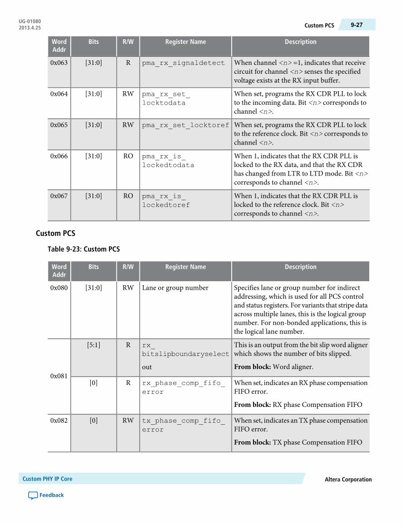
DescriptionRegister NameR/WBitsWordAddr
When channel <n> =1, indicates that receivecircuit for channel <n> senses the specifiedvoltage exists at the RX input buffer.
pma_rx_signaldetectR[31:0]0x063
When set, programs the RX CDR PLL to lockto the incoming data. Bit <n> corresponds tochannel <n>.
pma_rx_set_locktodata
RW[31:0]0x064
When set, programs the RX CDR PLL to lockto the reference clock. Bit <n> corresponds tochannel <n>.
pma_rx_set_locktorefRW[31:0]0x065
When 1, indicates that the RX CDR PLL islocked to the RX data, and that the RX CDRhas changed from LTR to LTD mode. Bit <n>corresponds to channel <n>.
pma_rx_is_lockedtodata
RO[31:0]0x066
When 1, indicates that the RX CDR PLL islocked to the reference clock. Bit <n>corresponds to channel <n>.
pma_rx_is_lockedtoref
RO[31:0]0x067
Custom PCS
Table 9-23: Custom PCS
DescriptionRegister NameR/WBitsWordAddr
Specifies lane or group number for indirectaddressing, which is used for all PCS controland status registers. For variants that stripe dataacross multiple lanes, this is the logical groupnumber. For non-bonded applications, this isthe logical lane number.
Lane or group numberRW[31:0]0x080
This is an output from the bit slip word alignerwhich shows the number of bits slipped.
From block: Word aligner.
rx_bitslipboundaryselect
out
R[5:1]
0x081When set, indicates anRXphase compensationFIFO error.
From block: RX phase Compensation FIFO
rx_phase_comp_fifo_error
R[0]
When set, indicates anTXphase compensationFIFO error.
From block: TX phase Compensation FIFO
tx_phase_comp_fifo_error
RW[0]0x082
Altera CorporationCustom PHY IP Core
Feedback
9-27Custom PCSUG-010802013.4.25

DescriptionRegister NameR/WBitsWordAddr
Sets the number of bits that the TX bit slipperneeds to slip.
To block: Word aligner.
tx_bitslipboundary_select
RW[5:1]
0x083When set, the TX interface inverts the polarityof the TX data.
To block: 8B/10B encoder.
tx_invpolarityRW[0]
When set, the RX channels inverts the polarityof the received data.
To block: 8B/10B decoder.
rx_invpolarityRW00x084
Every time this register transitions from 0 to 1,the RX data slips a single bit.
To block: Word aligner.
rx_bitslipRW[3]
0x085
When set, enables byte reversal on the RXinterface.
To block: Byte deserializer.
rx_bytereversal_enable
RW[2]
When set, enables bit reversal on the RXinterface.
To block: Word aligner.
rx_bitreversal_enable
RW[1]
When set inmanual word alignmentmode, theword alignment logic begins operation whenthis pattern is set.
To block: Word aligner.
rx_enapatternalignRW[0]
Dynamic ReconfigurationAs silicon progresses towards smaller process nodes, circuit performance is affected more by variations dueto process, voltage, and temperature (PVT). These process variations result in analog voltages that can beoffset from required ranges.The calibration performed by the dynamic reconfiguration interface compensates for variations due to PVT.
Each channel and each TX PLL have separate dynamic reconfiguration interfaces. The MegaWizard Plug-InManager provides informational messages on the connectivity of these interfaces. The following exampleshows the messages for a single duplex channel parameterized for the 1.25 GIGE protocol.
Although you must initially create a separate reconfiguration interface for each channel and TX PLL in yourdesign, when theQuartus II software compiles your design, it reduces the number of reconfiguration interfacesby merging reconfiguration interfaces. The synthesized design typically includes a reconfiguration interfacefor at least three channels because three channels share an Avalon-MM slave interface which connects tothe Transceiver Reconfiguration Controller IP Core. Conversely, you cannot connect the three channels
Custom PHY IP CoreAltera Corporation
Feedback
UG-01080Dynamic Reconfiguration9-28 2013.4.25

that share an Avalon-MM interface to different Transceiver Reconfiguration Controller IP Cores. Doing socauses a Fitter error.
Example 9-1: Informational Messages for the Transceiver Reconfiguration Interface
PHY IP will require 2 reconfiguration interfaces forconnection to the external reconfiguration controller.Reconfiguration interface offset 0 is connected to the transceiverchannel.Reconfiguration interface offset 1 is connected to the transmitPLL.
Table 9-24: Reconfiguration Interface
This interface uses the Avalon-MM PHY Management interface clock.DescriptionDirectionSignal Name
Reconfiguration signals from theTransceiver ReconfigurationController. <n> grows linearly withthe number of reconfigurationinterfaces.
Inputreconfig_to_xcvr [( <n>70-1):0]
Reconfiguration signals to theTransceiver ReconfigurationController. <n> grows linearly withthe number of reconfigurationinterfaces.
Outputreconfig_from_xcvr [(<n> 46-1):0]
Transceiver dynamic reconfiguration requires that you assign the starting channel number if you are using×6 or ×N bonding. Logical channel 0 should be assigned to either physical transceiver channel 1 or channel4 of a transceiver bank. However, if you have already created a PCB with a different lane assignment forlogical lane 0, you can use the workaound shown in the following example to remove this restriction. Theexample redefines thepma_bonding_master parameter using theQuartus II Assignment Editor. In thisexample, thepma_bonding_masterwasoriginally assigned tophysical channel 1. (Theoriginal assignmentcould also have been to physical channel 4.) The to parameter reassigns the pma_bonding_master tothe Custom PHY instance name. You must substitute the instance name from your design for the instancename shown in quotation marks
Example 9-2: Overriding Logical Channel 0 Channel Assignment Restrictions in Stratix V Devicesfor ×6 or ×N Bonding
set_parameter -name pma_bonding_master "\"1\"" -to"<custom phy instance>|altera_xcvr_custom:my_custom_phy_inst|sv_xcvr_custom_nr:S5|sv_xcvr_custom_native:transceiver_core|sv_xcvr_native:gen.sv_xcvr_native_insts[0].gen_bonded_group.sv_xcvr_native_inst"
Altera CorporationCustom PHY IP Core
Feedback
9-29Dynamic ReconfigurationUG-010802013.4.25

Related InformationTransceiver Reconfiguration Controller to PHY IP Connectivity on page 16-48
Custom PHY IP CoreAltera Corporation
Feedback
UG-01080Dynamic Reconfiguration9-30 2013.4.25

10Low Latency PHY IP Core
2013.4.25UG-01080 Subscribe Feedback
The Altera Low Latency PHY IP Core receives and transmits differential serial data, recovering the RX clockfrom the RX input stream. The PMA connects to a simplified PCS, which contains a phase compensationFIFO. Depending on the configuration you choose, the Low Latency PHY IP Core instantiates one of thefollowing channels:
• GX channels using the Standard PCS• GX channels using the 10G PCS• GT channels in PMA Direct mode
An Avalon-MM interface provides access to control and status information. The following figure illustratesthe top-level modules of the Low Latency PHY IP Core.
Figure 10-1: Low Latency PHY IP Core-Stratix V Devices
10GBASE-R PHY IP Core
10.3125 Gbps serialXFI/SFP+
Stratix V FPGA
PMA
Hard PCS10GBASE-R
64b/66bScramblerGearbox
SDR XGMII72 bits @ 156.25 Mbps
Avalon-MMControl & Status
TransceiverReconfiguraiton
Because the Low Latency PHY IP Core bypasses much of the PCS, it minimizes the PCS latency.
Formore detailed information about the LowLatency datapath and clocking, refer to the refer to the “StratixVGX Device Configurations” section in the Transceiver Configurations in Stratix V Devices chapter of theStratix V Device Handbook.
Related InformationTransceiver Configurations in Stratix V Devices
ISO9001:2008Registered
© 2013 Altera Corporation. All rights reserved. ALTERA, ARRIA, CYCLONE, HARDCOPY, MAX, MEGACORE, NIOS, QUARTUS and STRATIXwords and logos are trademarks of Altera Corporation and registered in the U.S. Patent and Trademark Office and in other countries. All other wordsand logos identified as trademarks or service marks are the property of their respective holders as described at www.altera.com/common/legal.html.Altera warrants performance of its semiconductor products to current specifications in accordance with Altera's standard warranty, but reserves theright to make changes to any products and services at any time without notice. Altera assumes no responsibility or liability arising out of the applicationor use of any information, product, or service described herein except as expressly agreed to in writing by Altera. Altera customers are advised toobtain the latest version of device specifications before relying on any published information and before placing orders for products or services.
www.altera.com
101 Innovation Drive, San Jose, CA 95134

Device Family SupportIP cores provide either final or preliminary support for target Altera device families. These terms have thefollowing definitions:
• Final support—Verified with final timing models for this device.• Preliminary support—Verified with preliminary timing models for this device.
The following table shows the level of support offered by the Low Latency PHY IP Core for Altera devicefamilies.
Table 10-1: Device Family Support
SupportDevice Family
PreliminaryArria V GZ devices
PreliminaryStratix V devices
No supportOther device families
Performance and Resource UtilizationThe following table shows the typical expected device resource utilization for different configurations usingthe current version of the Quartus II software targeting a Stratix V GX (5SGSMD612H35C2) device.
Table 10-2: Low Latency PHY Performance and Resource Utilization—Stratix V GX Device
Memory BitsDedicated Re-gisters
CombinationalALUTs
Worst-CaseFrequency
SerializationFactor
Number of
Lanes
Implementa-tion
095112599.1632 or 40111 Gbps
0117141584.832 or 40411 Gbps
0171192579.7132 or 401011 Gbps
093111608.2732 or 4016 Gbps(10 Gbpsdatapath)
0117141454.9632 or 4046 Gbps(10 Gbpsdatapath)
0171192562.7532 or 40106 Gbps(10 Gbpsdatapath)
093113607.1632 or 4016 Gbps (8Gbpsdatapath)
Low Latency PHY IP CoreAltera Corporation
Feedback
UG-01080Device Family Support10-2 2013.4.25

Memory BitsDedicated Re-gisters
CombinationalALUTs
Worst-CaseFrequency
SerializationFactor
Number of
Lanes
Implementa-tion
0117142639.832 or 4046 Gbps (8Gbpsdatapath)
0171193621.8932 or 40106 Gbps (8Gbpsdatapath)
093114673.48, 10, 16, or 2013 Gbps (8Gbpsdatapath)
0117142594.888, 10, 16, or 2043 Gbps (8Gbpsdatapath)
0171193667.678, 10, 16, or 20103 Gbps (8Gbpsdatapath)
.
Parameterizing the Low Latency PHYComplete the following steps to configure the LowLatency PHY IPCore in theMegaWizard Plug-InManager:
1. For Which device family will you be using ?, select Stratix V.2. Click IInstalled Plug Ins > Interfaces > Transceiver PHY > Low Latency PHY v12.1.3. Use the tabs on the MegaWizard Plug-In Manager to select the options required for the protocol.4. Refer to the following topics to learn more about the parameters:
• General Options Parameters on page 10-3• Additional Options Parameters on page 10-6• PLL Reconfiguration Parameters on page 10-9• Low Latency PHY Analog Parameters on page 10-10
5. Click Finish to generate your parameterized Low Latency PHY IP Core.
General Options ParametersThe following table lists the settings available on General Options tab:
Table 10-3: Low Latency PHY General Options
DescriptionValueName
This IP core is only available for Stratix V devices.Stratix VDevice family
Altera CorporationLow Latency PHY IP Core
Feedback
10-3Parameterizing the Low Latency PHYUG-010802013.4.25
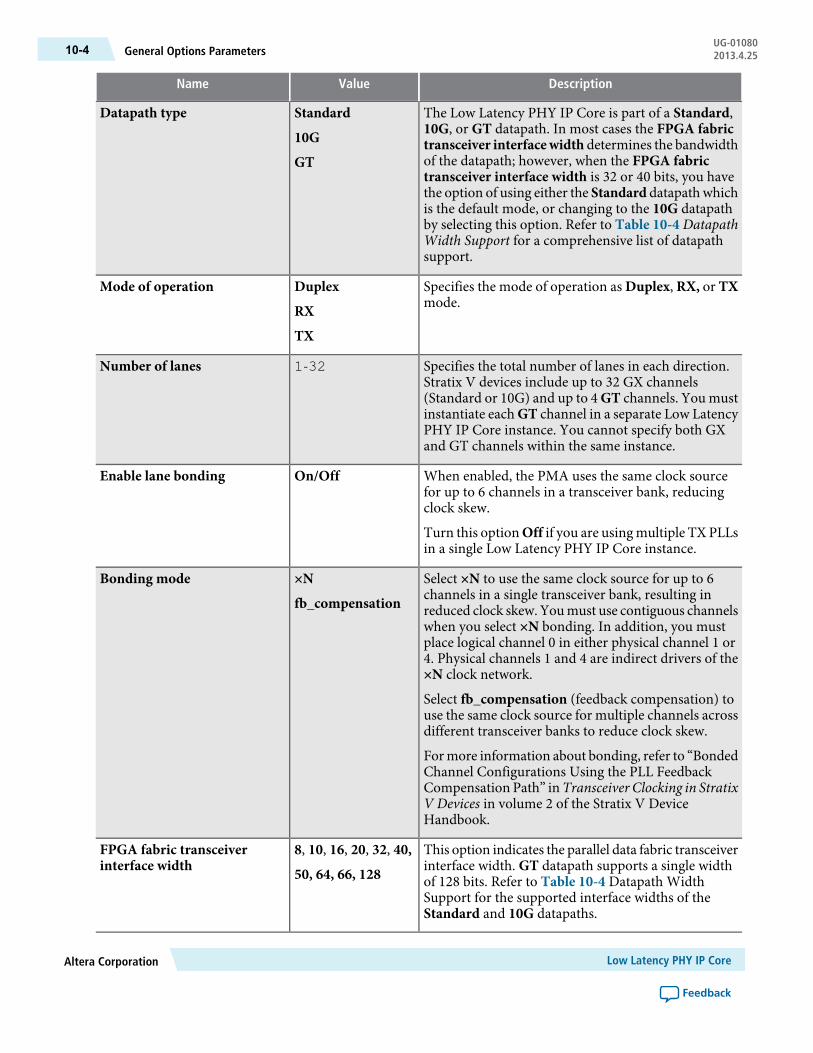
DescriptionValueName
The Low Latency PHY IP Core is part of a Standard,10G, or GT datapath. In most cases the FPGA fabrictransceiver interfacewidth determines the bandwidthof the datapath; however, when the FPGA fabrictransceiver interface width is 32 or 40 bits, you havethe option of using either the Standard datapathwhichis the default mode, or changing to the 10G datapathby selecting this option. Refer to Table 10-4 DatapathWidth Support for a comprehensive list of datapathsupport.
Standard
10G
GT
Datapath type
Specifies the mode of operation as Duplex, RX, or TXmode.
Duplex
RX
TX
Mode of operation
Specifies the total number of lanes in each direction.Stratix V devices include up to 32 GX channels(Standard or 10G) and up to 4 GT channels. You mustinstantiate each GT channel in a separate Low LatencyPHY IP Core instance. You cannot specify both GXand GT channels within the same instance.
1-32Number of lanes
When enabled, the PMA uses the same clock sourcefor up to 6 channels in a transceiver bank, reducingclock skew.
Turn this optionOff if you are using multiple TX PLLsin a single Low Latency PHY IP Core instance.
On/OffEnable lane bonding
Select ×N to use the same clock source for up to 6channels in a single transceiver bank, resulting inreduced clock skew. Youmust use contiguous channelswhen you select ×N bonding. In addition, you mustplace logical channel 0 in either physical channel 1 or4. Physical channels 1 and 4 are indirect drivers of the×N clock network.
Select fb_compensation (feedback compensation) touse the same clock source for multiple channels acrossdifferent transceiver banks to reduce clock skew.
Formore information about bonding, refer to “BondedChannel Configurations Using the PLL FeedbackCompensation Path” inTransceiver Clocking in StratixV Devices in volume 2 of the Stratix V DeviceHandbook.
×N
fb_compensation
Bonding mode
This option indicates the parallel data fabric transceiverinterface width. GT datapath supports a single widthof 128 bits. Refer to Table 10-4 Datapath WidthSupport for the supported interface widths of theStandard and 10G datapaths.
8, 10, 16, 20, 32, 40,
50, 64, 66, 128
FPGA fabric transceiverinterface width
Low Latency PHY IP CoreAltera Corporation
Feedback
UG-01080General Options Parameters10-4 2013.4.25
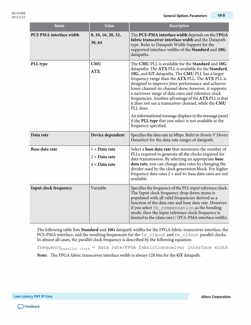
DescriptionValueName
The PCS-PMA interface width depends on the FPGAfabric transceiver interface width and the Datapathtype. Refer to Datapath Width Support for thesupported interface widths of the Standard and 10Gdatapaths.
8, 10, 16, 20, 32,
30, 64
PCS PMA interface width
The CMU PLL is available for the Standard and 10Gdatapaths. The ATX PLL is available for the Standard,10G, and GT datapaths. The CMU PLL has a largerfrequency range than the ATX PLL. The ATX PLL isdesigned to improve jitter performance and achieveslower channel-to-channel skew; however, it supportsa narrower range of data rates and reference clockfrequencies. Another advantage of theATXPLL is thatit does not use a transceiver channel, while the CMUPLL does.
An informationalmessage displays in themessage panelif the PLL type that you select is not available at thefrequency specified.
CMU
ATX
PLL type
Specifies the data rate inMbps. Refer to Stratix VDeviceDatasheet for the data rate ranges of datapath.
Device dependentData rate
Select a base data rate that minimizes the number ofPLLs required to generate all the clocks required fordata transmission. By selecting an appropriate basedata rate, you can change data rates by changing thedivider used by the clock generation block. For higherfrequency data rates 2 × and 4× base data rates are notavailable.
1 × Data rate
2 × Data rate
4 × Data rate
Base data rate
Specifies the frequency of the PLL input reference clock.The Input clock frequency drop down menu ispopulated with all valid frequencies derived as afunction of the data rate and base data rate. However,if you select fb_compensation as the bondingmode, then the input reference clock frequency islimited to the (data rate) / (PCS-PMA interface width).
VariableInput clock frequency
The following table lists Standard and 10G datapath widths for the FPGA fabric-transceiver interface, thePCS-PMA interface, and the resulting frequencies for the tx_clkout and rx_clkout parallel clocks.In almost all cases, the parallel clock frequency is described by the following equation:
frequencyparallel clock = data rate/FPGA fabrictransceiver interface width
The FPGA fabric transceiver interface width is always 128 bits for the GT datapath.Note:
Altera CorporationLow Latency PHY IP Core
Feedback
10-5General Options ParametersUG-010802013.4.25

Table 10-4: Datapath Width Support
tx_clkout and rx_clkout frequencyPCS-PMA Interface WidthFPGA Fabric - Trans-
ceiver Interface Width 10G DatapathStandard Datapath
data rate/8—88
data rate/10—1010
data rate/16—8 or 1616
data rate/20—10 or 2020
data rate/32321632
data rate/40402040
data rate/50 (1)40—50
data rate/32 (2)32—64
data rate/6464—64
data rate/6640—66
Table Notes:
1. For this datapath configuration, the tx_clkout frequency generated by the Low Latency PHY is the datarate /40. You must generate a /50 frequency clock from the /40 clock and feed this clock back into the tx_coreclkin. The rx_clkout frequency generated by the Low Latency PHY is /40 of the data rate. Youmust generate a /50 frequency from the recovered clock and feed this back into the rx_coreclkin.
2. For this datapath configuration, the tx_clkout frequency generated by the Low Latency PHY is the datarate/32. You must generate a /64 frequency clock from the /32 clock and feed this clock back into the tx_coreclkin. The rx_clkout frequency generated by the Low Latency PHY is the data rate/32. Youmust generate a /64 frequency from the recovered clock and feed this back into the rx_coreclkin
Related InformationStratix V Device Datasheet
Transceiver Clocking in Stratix V Devices
Additional Options ParametersThe parameters on the Additional Options tab control clocking and datapath options. Both bonded (×N)and non-bonded modes are available. In bonded modes, a single PLL can drive all channels. In non-bondedmodes, each channel may have its own PLL.
Low Latency PHY IP CoreAltera Corporation
Feedback
UG-01080Additional Options Parameters10-6 2013.4.25

The following table describes the options available on the Additional Options tab:
Table 10-5: Additional Options
DescriptionValueName
When you turn this option on, tx_coreclkin connectsto the write clock of the TX phase compensation FIFO andyou can clock the parallel TX data generated in the FPGAfabric using this port. This port allows you to clock the writeside of the TX phase compensation FIFO with auser-provided clock, either the FPGA fabric clock, the FPGAfabric-TX interface clock, or the input reference clock. Youmust turn this optionOnwhen the FPGA fabric transceiverinterfacewidth:PCS-PMA interfacewidth is 50:40 orwhenyou specify the 10G datapath with a fabric transceiverinterface width:PCS-PMA interface width of 64:32.
For the GT datapath, if you are using different referenceclock pins for the TX andRX channels, youmust instantiatetwo separate Low Latency PHY IP Core instances for TXand RX channels. The reference clock pins for each channelmust reside in the same transceiver bank.
Formore information refer to the “FPGAFabric-TransceiverInterface Clocking” section in the Stratix V TransceiverClocking chapter.
On/OffEnable tx_coreclkin
When you turn this option on, rx_coreclkin connectsto the read clock of the RX phase compensation FIFO andyou can clock the parallel RX output data using rx_coreclk. This port allows you to clock the read side of theRX phase compensation FIFO with a userprovided clock,either the FPGA fabric clock, the FPGA fabric RX interfaceclock, or the input reference clock. rx_coreclkin is notavailable for the GT datapath.
You must turn this option On when the FPGA fabrictransceiver interface width:PCS-PMA Interface width is50:40 or when you specify the 10G datapath with a fabrictransceiver interface width:PCS-PMA Interface width of64:32.
Formore information refer to the “FPGAFabric-TransceiverInterface Clocking” section in the Stratix V TransceiverClocking chapter.
On/OffEnable rx_coreclkin
Altera CorporationLow Latency PHY IP Core
Feedback
10-7Additional Options ParametersUG-010802013.4.25

DescriptionValueName
The bit slip feature allows you to slip the transmitter sidebits before they are sent to the gearbox. The maximumnumber of bits slipped is equal to the ((FPGAfabric-to-transceiver interface width) – 1). For example, ifthe FPGA fabric-to-transceiver interface width is 64 bits,the bit slip logic can slip amaximumof 63 bits. Each channelhas 5 bits to determine the number of bits to slip. The valuespecified on the TX bitslip bus indicates the number of bitslips. Effectively, each value shifts the word boundary by onebit. For example, a TX bitslip value of 1 on a 64bit FPGAinterface width shifts the word boundary by 1 bit. That is,bit[63] from the first word and bit[62:0] are concatenatedto form a 64 bit word (bit[62:0] from the second word,bit[63] from the first word LSB).
This option is only available for the Standard and 10Gdatapaths.
On/OffEnable TX bitslip
When enabled, the wordaligner operates in bitslip mode.This option is available for Stratix V andArria VGZdevicesusing the 10G datapath.
On/OffEnable RX bitslip
This option is turned on by default.WhenOn, the embeddedreset controller initiates the reset sequence when it receivesa positive edge on the phy_mgmt_clk_reset inputsignal.
Disable this option to implement your own reset sequenceusing the tx_analogreset, rx_analogreset, tx_digitalreset, rx_digitalreset, and pll_powerdown which are available as top-level ports of theLow Latency Transceiver PHY. When you design your ownreset controller, the tx_ready and rx_ready are nottop-level signals of the core. Another option is to useAltera’sTransceiver PHY Reset Controller IP Core to reset thetransceivers. For more information, refer to the TransceiverPHY Reset Controller IP Corechapter.
For more information about designing a reset controller,refer to the User-Controlled Reset Controller section in theTransceiver Reset Control in Stratix V Devices in volume 2of the Stratix V Device Handbook.
On/OffEnable embedded resetcontrol
When you turn this option On, the order of symbols ischanged. This option is typically required if you are planningto import your Low Latency Transceiver PHY IP Core intoa Qsys system.
On/OffAvalon data interfaces
Related InformationStratix V Transceiver Clocking
Transceiver Reset Control in Stratix V Devices
Low Latency PHY IP CoreAltera Corporation
Feedback
UG-01080Additional Options Parameters10-8 2013.4.25
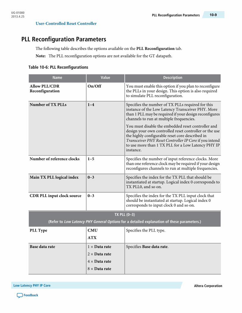
User-Controlled Reset Controller
PLL Reconfiguration ParametersThe following table describes the options available on the PLL Reconfiguration tab.
The PLL reconfiguration options are not available for the GT datapath.Note:
Table 10-6: PLL Reconfigurations
DescriptionValueName
You must enable this option if you plan to reconfigurethe PLLs in your design. This option is also requiredto simulate PLL reconfiguration.
On/OffAllow PLL/CDRReconfiguration
Specifies the number of TX PLLs required for thisinstance of the Low Latency Transceiver PHY. Morethan 1 PLLmay be required if your design reconfigureschannels to run at multiple frequencies.
You must disable the embedded reset controller anddesign your own controlled reset controller or the usethe highly configurable reset core described inTransceiver PHY Reset Controller IP Core if you intendto use more than 1 TX PLL for a Low Latency PHY IPinstance.
1–4Number of TX PLLs
Specifies the number of input reference clocks. Morethan one reference clockmay be required if your designreconfigures channels to run at multiple frequencies.
1–5Number of reference clocks
Specifies the index for the TX PLL that should beinstantiated at startup. Logical index 0 corresponds toTX PLL0, and so on.
0–3Main TX PLL logical index
Specifies the index for the TX PLL input clock thatshould be instantiated at startup. Logical index 0corresponds to input clock 0 and so on.
0–3CDR PLL input clock source
TX PLL (0–3)
(Refer to Low Latency PHY General Options for a detailed explanation of these parameters.)
Specifies the PLL type.CMU
ATX
PLL Type
Specifies Base data rate.1 × Data rate
2 × Data rate
4 × Data rate
8 × Data rate
Base data rate
Altera CorporationLow Latency PHY IP Core
Feedback
10-9PLL Reconfiguration ParametersUG-010802013.4.25
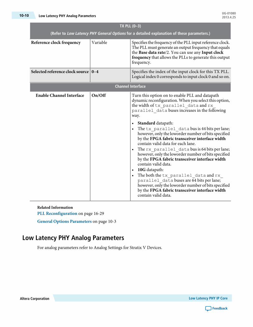
TX PLL (0–3)
(Refer to Low Latency PHY General Options for a detailed explanation of these parameters.)
Specifies the frequency of the PLL input reference clock.The PLLmust generate an output frequency that equalsthe Base data rate/2. You can use any Input clockfrequency that allows the PLLs to generate this outputfrequency.
VariableReference clock frequency
Specifies the index of the input clock for this TX PLL.Logical index 0 corresponds to input clock 0 and so on.
0–4Selected reference clock source
Channel Interface
Turn this option on to enable PLL and datapathdynamic reconfiguration.When you select this option,the width of tx_parallel_data and rx_parallel_data buses increases in the followingway.
• Standard datapath:• The tx_parallel_data bus is 44 bits per lane;
however, only the loworder number of bits specifiedby the FPGA fabric transceiver interface widthcontain valid data for each lane.
• The rx_parallel_data bus is 64 bits per lane;however, only the loworder number of bits specifiedby the FPGA fabric transceiver interface widthcontain valid data.
• 10G datapath:• The both the tx_parallel_data and rx_
parallel_data buses are 64 bits per lane;however, only the loworder number of bits specifiedby the FPGA fabric transceiver interface widthcontain valid data.
On/OffEnable Channel Interface
Related InformationPLL Reconfiguration on page 16-29
General Options Parameters on page 10-3
Low Latency PHY Analog ParametersFor analog parameters refer to Analog Settings for Stratix V Devices.
Low Latency PHY IP CoreAltera Corporation
Feedback
UG-01080Low Latency PHY Analog Parameters10-10 2013.4.25

Related InformationAnalog Settings for Arria V GZ Devices on page 19-9
Analog Settings for Stratix V Devices on page 19-25
Low Latency PHY InterfacesThe following figure illustrates the top-level signals of the Custom PHY IP Core. The variables in this figurerepresent the following parameters:
• <n>—The number of lanes• <w>—The width of the FPGA fabric to transceiver interface per lane
Figure 10-2: Top-Level Low Latency Signals
Low Latency PHY IP Core Top-Level Signals
tx_serial_data<n>rx_serial_data<n>
rx_is_lockedtodata[<n>-1:0]rx_is_lockedtoref[<n>-1:0]
pll_locked[<n>-1:0]tx_bitsliprx_bitslip
pll_powerdowntx_digitalreset<n>tx_analogreset<n>
tx_cal_busy<n>rx_digitalreset<n>rx_analogreset<n>
rx_cal_busy<n>
reconfig_to_xcvr[(<n>70-1):0]reconfig_from_xcvr[(<n>46-1):0]
Control andStatus
(Optional)
tx_parallel_data[<n><w>-1:0]tx_clkout[<n>-1:0]rx_parallel_data[<n><w>-1:0]rx_clkout[<n>-1:0]tx_ready[<n>-1:0]rx_ready[<n>-1:0]
phy_mgmt_clkphy_mgmt_clk_resetphy_mgmt_address[8:0]phy_mgmt_writedata[31:0]phy_mgmt_readdata[31:0]phy_mgmt_writephy_mgmt_readphy_mgmt_waitrequest
pll_ref_clktx_coreclkin[<n>-1:0]rx_coreclkin[<n>-1:0]
Avalon-MM PHYManagementInterface
Avalon-ST TX and RXto and from MAC
SerialData
DynamicReconfiguration
Reset Controland Status(Optional)
Clocks Optional
By default block diagram shown in the MegaWizard Plug-In Manager labels the external pins withthe interface type and places the interface name inside the box. The interface type and name are used
Note:
in the _hw.tcl file that describes the component. If you turn on Show signals, the block diagramdisplays all toplevel signal names.
For more information about _hw.tcl files refer to refer to the Component Interface Tcl Reference chapterin volume 1 of the Quartus II Handbook.
Low Latency PHY Data InterfacesThe following table describes the signals in the Avalon-ST interface. This interface drives AvalonST TX andRX data to and from the FPGA fabric. These signals are named from the point of view of the MAC so thatthe TX interface is an Avalon-ST sink interface and the RX interface is an Avalon-ST source.
Altera CorporationLow Latency PHY IP Core
Feedback
10-11Low Latency PHY InterfacesUG-010802013.4.25

Table 10-7: Avalon-ST interface
DescriptionDirectionSignal Name
This is TX parallel data driven from the MAC FPGAfabric. The ready latency on this interface is 0, so thatthe PCS in Low-Latency Bypass Mode or the MAC inPMA Direct mode must be able to accept data as soonas it comes out of reset.
Inputtx_parallel_data[<n><w>-1:0]
This is the clock for TX parallel data.Outputtx_clkout[<n>-1:0]
When asserted, indicates that the Low Latency IP Corehas exited the reset state is ready to receive data fromthe MAC. This signal is available if you select Enableembedded reset control on the Additional Optionstab.
Outputtx_ready[<n>-1:0]
This is RX parallel data driven by the LowLatency PHYIP Core. Data driven from this interface is always valid.
Outputrx_parallel_data [ <n><w>-1:0]
Low speed clock recovered from the serial data.Outputrx_clkout[<n>-1:0]
This is the ready signal for the RX interface. The readylatency on this interface is 0, so that the MAC must beable to accept data as soon as the PMA comes out ofreset. This signal is available if you select Enableembedded reset control on the Additional Optionstab.
Outputrx_ready[<n>-1:0]
The following table describes the signals that comprise the serial data interface:
Table 10-8: Serial Data Interface
DescriptionDirectionSignal Name
Differential high speed input serial data.Inputrx_serial_data[<n>-1:0]
Differential high speed output serial data.Outputtx_serial_data[<n>-1:0]
Low Latency PHY IP CoreAltera Corporation
Feedback
UG-01080Low Latency PHY Data Interfaces10-12 2013.4.25

Optional Status InterfaceThe following table describes the signals that comprise the optional status interface:
Table 10-9: Optional Status Interface
DescriptionDirectionSignal Name
When asserted, indicates that the RX CDR is lockedto incoming data. This signal is optional. If latencyis not critical, you can read the value of this signalfrom the Rx_is_lockedtodata register.
Outputrx_is_lockedtodata[<n>-1:0]
When asserted, indicates that the RX CDR is lockedto the input reference clock. This signal is optional.When the RX CDR is locked to data, you can ignoretransitions on this signal. If latency is not critical,you can read the value of this signal from the rx_is_lockedtoref register.
Outputrx_is_lockedtoref[<n>-1:0]
When asserted, indicates that the TX PLL is lockedto the input reference clock. This signal isasynchronous.
Outputpll_locked[<n>-1:0]
When set, the data sent to the PMA is slipped. Themaximumnumber of bits that can be slipped is equalto the value selected in the serialization factor field- 1 or <d> -1.
Inputtx_bitslip[<n>-1:0]
When set, the RX word aligner operates in bit slipmode.
Inputrx_bitslip[<n>-1:0]
Low Latency PHY Clock InterfaceThe following table describes reference clock for the Low Latency PHY. The input reference clock,pll_ref_clk, drives a PLL inside the PHY-layer block, and a PLL output clock, rx_clkout is used forall data, command, and status inputs and outputs.
Altera CorporationLow Latency PHY IP Core
Feedback
10-13Optional Status InterfaceUG-010802013.4.25

Table 10-10: Clock Signals
DescriptionDirectionSignal Name
This is an optional clock to drive the write side of theTX FIFO.
Inputtx_coreclkin[<n>-1:0]
This is an optional clock to drive the read side of theRX FIFO.
Inputrx_coreclkin[<n>-1:0]
Reference clock for the PHYPLLs. The frequency rangeis 60–700 MHz.
Inputpll_ref_clk
Optional Reset Control and Status InterfaceThe following table describes the signals in the optional reset control and status interface. These signals areavailable if you donot enable the embedded reset controller. Formore information including timing diagrams,refer to Transceiver Reset Control in Stratix V Devices in volume 2 of the Stratix V Device Handbook.
Table 10-11: Avalon-ST RX Interface
DescriptionDirectionSignal Name
When asserted, resets the TX PLL.Inputpll_powerdown
When asserted, reset all blocks in the TX PCS. Ifyour design includes bondedTXPCS channels, referto Timing Constraints for Reset Signals when UsingBonded PCS Channels for a SDC constraint youmust include in your design.
Inputtx_digitalreset[<n>-1:0]
When asserted, resets all blocks in the TX PMA.Inputtx_analogreset[<n>-1:0]
When asserted, indicates that theTX channel is beingcalibrated. You must hold the channel in reset untilcalibration completes.
Outputtx_cal_busy[<n>-1:0]
When asserted, resets the RX PCS.Inputrx_digitalreset[<n>-1:0]
When asserted, resets the RX CDR.Inputrx_analogreset[<n>-1:0]
When asserted, indicates that theRX channel is beingcalibrated. You must hold the channel in reset untilcalibration completes.
Outputrx_cal_busy[<n>-1:0]
Low Latency PHY IP CoreAltera Corporation
Feedback
UG-01080Optional Reset Control and Status Interface10-14 2013.4.25

Related InformationTiming Constraints for Reset Signals when Using Bonded PCS Channels on page 17-10
Register Interface and Register DescriptionsThe Avalon-MM PHY management interface provides access to the Low Latency PHY PCS and PMAregisters that control the TX and RX channels, the PMA powerdown, PLL registers, and loopback modes.The following figure provides a highlevel view of this hardware.
Figure 10-3: PMA Top-Level Modules
PMA and Light-Weight PCS
DynamicReconfiguration
Native PMAControl
ChannelControlS
Avalon-MMControl
S
S
Low LatencyPHY Controller
Tx Data
to EmbeddedController
TransceiverReconfiguration
Controller
to and fromUser Logic
Tx Parallel DataRx Data
Rx Parallel Data
MAvalon-MM
PHYMgmt
S
Rx Serial Data
Tx Serial Data <n>
<n>
Altera CorporationLow Latency PHY IP Core
Feedback
10-15Register Interface and Register DescriptionsUG-010802013.4.25

The following table describes the signals in the PHY Management interface:
Table 10-12: Avalon-MM PHY Management Interface
DescriptionDirectionSignal Name
Avalon-MM clock input. There is no frequencyrestriction for the phy_mgmt_clk; however, if youplan to use the same clock for the PHY managementinterface and transceiver reconfiguration, you mustrestrict the frequency range of phy_mgmt_clk to100–150 MHz to meet the specification for thetransceiver reconfiguration clock.
Inputphy_mgmt_clk
Global reset signal. This signal is active high and levelsensitive. This is an asynchronous signal.
Inputphy_mgmt_clk_reset
9-bit Avalon-MM address.Inputphy_mgmtaddress[8:0]
Input data.Inputphy_mgmt_writedata[31:0]
Output data.Outputphy_mgmt_readdata[31:0]
Write signal.Inputphy_mgmt_write
Read signal.Inputphy_mgmt_read
For more information about the Avalon-MM and Avalon-ST protocols, including timing diagrams, referto the Avalon Interface Specifications .
The following table describes the registers that you can access over the PHY Management Interface usingword addresses and a 32-bit embedded processor.
Writing to reserved or undefined register addresses may have undefined side effects.Note:
Low Latency PHY IP CoreAltera Corporation
Feedback
UG-01080Register Interface and Register Descriptions10-16 2013.4.25
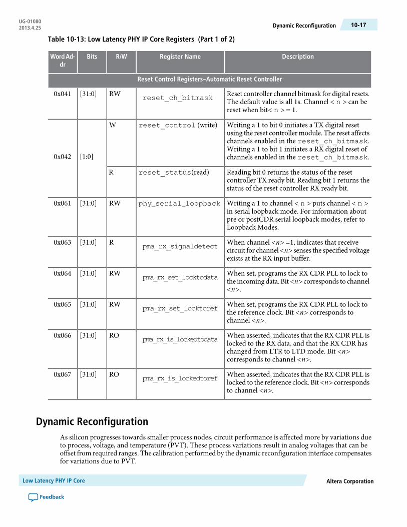
Table 10-13: Low Latency PHY IP Core Registers (Part 1 of 2)
DescriptionRegister NameR/WBitsWord Ad-dr
Reset Control Registers–Automatic Reset Controller
Reset controller channel bitmask for digital resets.The default value is all 1s. Channel < n > can bereset when bit< n > = 1.
reset_ch_bitmaskRW[31:0]0x041
Writing a 1 to bit 0 initiates a TX digital resetusing the reset controllermodule. The reset affectschannels enabled in the reset_ch_bitmask.Writing a 1 to bit 1 initiates a RX digital reset ofchannels enabled in the reset_ch_bitmask.
reset_control (write)W
[1:0]0x042
Reading bit 0 returns the status of the resetcontroller TX ready bit. Reading bit 1 returns thestatus of the reset controller RX ready bit.
reset_status(read)R
Writing a 1 to channel < n > puts channel < n >in serial loopback mode. For information aboutpre or postCDR serial loopback modes, refer toLoopback Modes.
phy_serial_loopbackRW[31:0]0x061
When channel <n> =1, indicates that receivecircuit for channel<n> senses the specified voltageexists at the RX input buffer.
pma_rx_signaldetectR[31:0]0x063
When set, programs the RX CDR PLL to lock tothe incomingdata. Bit<n> corresponds to channel<n>.
pma_rx_set_locktodataRW[31:0]0x064
When set, programs the RX CDR PLL to lock tothe reference clock. Bit <n> corresponds tochannel <n>.
pma_rx_set_locktorefRW[31:0]0x065
When asserted, indicates that the RX CDR PLL islocked to the RX data, and that the RX CDR haschanged from LTR to LTD mode. Bit <n>corresponds to channel <n>.
pma_rx_is_lockedtodataRO[31:0]0x066
When asserted, indicates that the RX CDR PLL islocked to the reference clock. Bit<n> correspondsto channel <n>.
pma_rx_is_lockedtorefRO[31:0]0x067
Dynamic ReconfigurationAs silicon progresses towards smaller process nodes, circuit performance is affected more by variations dueto process, voltage, and temperature (PVT). These process variations result in analog voltages that can beoffset from required ranges. The calibration performed by the dynamic reconfiguration interface compensatesfor variations due to PVT.
Altera CorporationLow Latency PHY IP Core
Feedback
10-17Dynamic ReconfigurationUG-010802013.4.25
Each channel and each TX PLL have separate dynamic reconfiguration interfaces. The MegaWizard Plug-InManager provides informational messages on the connectivity of these interfaces. The following exampleshows the messages for a single duplex channel.
Example 10-1: Informational Messages for the Transceiver Reconfiguration Interface
PHY IP will require 2 reconfiguration interfaces for connection to the external reconfigurationcontroller.
Reconfiguration interface offset 0 is connected to the transceiver channel.
Reconfiguration interface offset 1 is connected to the transmit PLL.
Although you must initially create a separate reconfiguration interface for each channel and TX PLL in yourdesign, when theQuartus II software compiles your design, it reduces the number of reconfiguration interfacesby merging reconfiguration interfaces. The synthesized design typically includes a reconfiguration interfacefor at least three channels because three channels share an Avalon-MM slave interface which connects tothe Transceiver Reconfiguration Controller IP Core. Conversely, you cannot connect the three channelsthat share an Avalon-MM interface to different Transceiver Reconfiguration Controller IP Cores. Doing socauses a Fitter error. For more information, refer to Transceiver Reconfiguration Controller to PHY IPConnectivity.
The following table describes the signals in the reconfiguration interface. This interface uses a clock providedby the reconfiguration controller.
Table 10-14: Reconfiguration Interface
DescriptionDirectionSignal Name
Reconfiguration signals from the TransceiverReconfiguration Controller. <n> grows linearly withthe number of reconfiguration interfaces.
Inputreconfig_to_xcvr[(<n>70)-1:0]
Reconfiguration signals to the TransceiverReconfiguration Controller. <n> grows linearly withthe number of reconfiguration interfaces.
Outputreconfig_from_xcvr[(<n>46)-1:0]
If you are using ×6 or ×N bonding, transceiver dynamic reconfiguration requires that you assign the startingchannel number. Logical channel 0 should be assigned to either physical transceiver channel 1 or channel4 of a transceiver bank. However, if you have already created a PCB with a different lane assignment forlogical lane 0, you can use the workaound shown in The following example to remove this restriction. Thisexample redefines thepma_bonding_master parameter using theQuartus II Assignment Editor. In thisexample, thepma_bonding_masterwasoriginally assigned tophysical channel 1. (Theoriginal assignmentcould also have been to physical channel 4.) The to parameter reassigns the pma_bonding_master tothe Low Latency PHY instance name. You must substitute the instance name from your design for theinstance name shown in quotation marks.
Example 10-2: Overriding Logical Channel 0 Channel Assignment Restrictions in Stratix V Devicesfor ×6 or ×N Bonding
set_parameter -name pma_bonding_master "\"1\"" -to "<low latency phy instance>
Low Latency PHY IP CoreAltera Corporation
Feedback
UG-01080Dynamic Reconfiguration10-18 2013.4.25
|altera_xcvr_low_latency_phy:my_low_latency_phy_inst|sv_xcvr_low_latency_phy_nr:
sv_xcvr_low_latency_phy_nr_inst|sv_xcvr_10g_custom_native:sv_xcvr_10g_custom_native_inst
|sv_xcvr_native:sv_xcvr_native_insts[0].gen_bonded_group_native.sv_xcvr_native_inst"
Simulation Files and Example TestbenchRefer to Running a Simulation Testbench for a description of the directories and files that the Quartus IIsoftware creates automatically when you generate your Low Latency PHY IP Core.
Refer to the Altera wiki for an example testbench that you can use as a starting point in creating your ownverification environment.
Altera CorporationLow Latency PHY IP Core
Feedback
10-19Simulation Files and Example TestbenchUG-010802013.4.25

11Deterministic Latency PHY IP Core
2013.4.25UG-01080 Subscribe Feedback
Deterministic latency enables accurate delay measurements and known timing for the transmit (TX) andreceive (RX) datapaths as required in applications such as wireless communication systems, emergingEthernet standards, and test and measurement equipment. The Deterministic Latency PHY IP Core support1-32 lanes with a continuous range of data rates from 611–6144 Mbps for Arria V devices, 0.6222–6.144Gbps inArria VGZ, 611–5000Mbps in CycloneV devices, and 611Mbps–12200Mbps for Stratix V devices.By setting the appropriate options using the MegaWizard Plug-In Manager, you can configure theDeterministic Latency PHY IPCore to supportmany industry-standard protocols that require deterministiclatency, including the following protocols:
• Common Public Radio Interface (CPRI)• Open Base Station Architecture Initiative (OBSAI)• 1588 Ethernet
For more information about using the Deterministic Latency PHY IP Core to implement CPRI, refer to theapplication note, Implementing the CPRI Protocol Using the Deterministic PHY IP Core.
The following figure illustrates the top-level interfaces and modules of the Deterministic Latency PHY IPCore. As the figure shows, the physical coding sublayer (PCS) includes the following functions:
• TX and RX Phase Compensation FIFO• Byte serializer and deserializer• 8B/10B encoder and decoder• Word aligner• TX bit slipper
ISO9001:2008Registered
© 2013 Altera Corporation. All rights reserved. ALTERA, ARRIA, CYCLONE, HARDCOPY, MAX, MEGACORE, NIOS, QUARTUS and STRATIXwords and logos are trademarks of Altera Corporation and registered in the U.S. Patent and Trademark Office and in other countries. All other wordsand logos identified as trademarks or service marks are the property of their respective holders as described at www.altera.com/common/legal.html.Altera warrants performance of its semiconductor products to current specifications in accordance with Altera's standard warranty, but reserves theright to make changes to any products and services at any time without notice. Altera assumes no responsibility or liability arising out of the applicationor use of any information, product, or service described herein except as expressly agreed to in writing by Altera. Altera customers are advised toobtain the latest version of device specifications before relying on any published information and before placing orders for products or services.
www.altera.com
101 Innovation Drive, San Jose, CA 95134

Figure 11-1: Deterministic Latency PHY IP Core
Deterministic Latency PHY IP Core
Arria V, Cyclone V, or Stratix V FPGA
PCS:
Phase Comp FIFOsByte Serializer/
Deserializer8B/10B
Word AlignerBit Slipper
PMA:
CDRSerializer
Deserializer
TX Serial DataRX Serial Data
toOptical
LinkAvalon-ST TX and RX
Avalon-MM Cntrl and Status
to and fromTransceiver Reconfiguration
Controller
The data that the Deterministic Latency PHY receives data on its FPGA fabric interface employs the AvalonStreaming (Avalon-ST) protocol to transmit and receive data. The Avalon-ST protocol is a simple protocoldesigned for driving high bandwidth, low latency, unidirectional data. The Deterministic Latency PHY IPCore also includes anAvalonMemory-Mapped (Avalon-MM) interface to access control and status registers.This is a standard, memory-mapped protocol that is normally used to read and write registers and memory.The transceiver reconfiguration interface connects to the Altera Transceiver Reconfiguration Controller IPCore which can dynamically reconfigure transceiver settings. Finally, the PMA transmits and receives serialdata.
Related InformationImplementing the CPRI Protocol Using the Deterministic PHY IP Core
Avalon Interface Specifications
Deterministic Latency Auto-NegotiationThe Deterministic Latency PHY IP Core supports auto-negotiation. When required, the channels initializeat the highest supported frequency and switch to successively lower data rates if frame synchronization isnot achieved.
If your design requires auto-negotiation, choose a base data rate that minimizes the number of PLLs requiredto generate the clocks required for data transmission. By selecting an appropriate base data rate, you canchange data rates by changing the divider used by the clock generation block. The following table shows anexample where setting two base data rates, 4915.2 and 6144 Mbps, with the appropriate clock dividersgenerates almost the full range of data rates required by the CPRI protocol.
Table 11-1: Recommended Base Data Rate and Clock Divisors for CPRI
Clock DividerBase Data Rate (Mbps)Data Rate (Mbps)
84915.2614.4
44915.21228.8
24915.22457.6
26144.03072.0
Deterministic Latency PHY IP CoreAltera Corporation
Feedback
UG-01080Deterministic Latency Auto-Negotiation11-2 2013.4.25
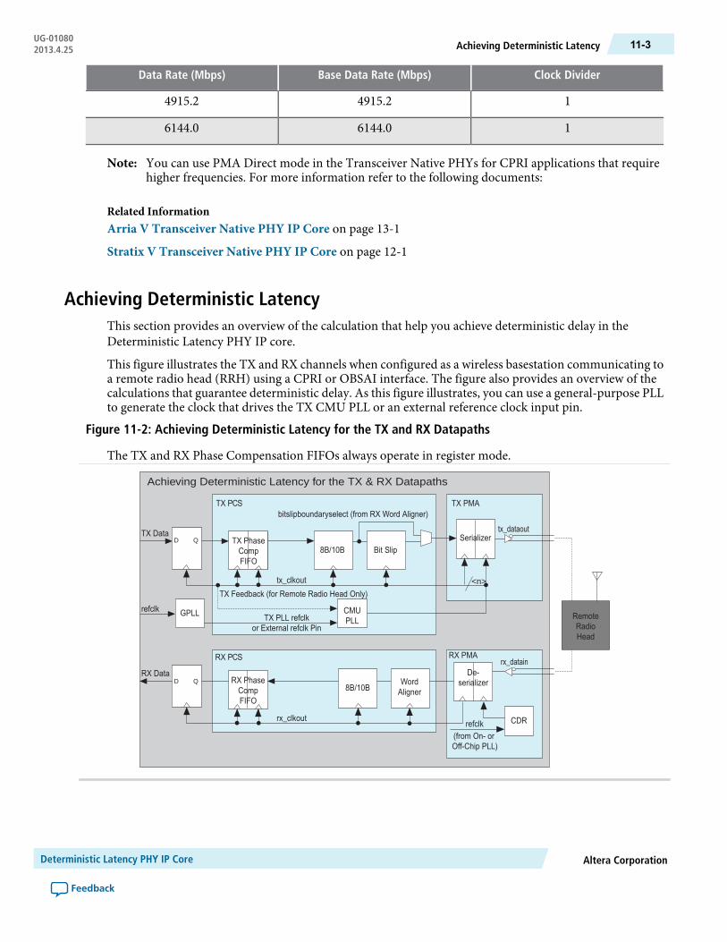
Clock DividerBase Data Rate (Mbps)Data Rate (Mbps)
14915.24915.2
16144.06144.0
You can use PMA Direct mode in the Transceiver Native PHYs for CPRI applications that requirehigher frequencies. For more information refer to the following documents:
Note:
Related InformationArria V Transceiver Native PHY IP Core on page 13-1
Stratix V Transceiver Native PHY IP Core on page 12-1
Achieving Deterministic LatencyThis section provides an overview of the calculation that help you achieve deterministic delay in theDeterministic Latency PHY IP core.
This figure illustrates the TX and RX channels when configured as a wireless basestation communicating toa remote radio head (RRH) using a CPRI or OBSAI interface. The figure also provides an overview of thecalculations that guarantee deterministic delay. As this figure illustrates, you can use a general-purpose PLLto generate the clock that drives the TX CMU PLL or an external reference clock input pin.
Figure 11-2: Achieving Deterministic Latency for the TX and RX Datapaths
The TX and RX Phase Compensation FIFOs always operate in register mode.
TX Data
RX Data
bitslipboundaryselect (from RX Word Aligner)TX PMA
tx_dataoutD Q
D Q
Serializer
RX PMA
De-serializer
CMUPLL
GPLL
CDR
refclk
refclk(from On- orOff-Chip PLL)
<n>
8B/10B
rx_datainRX PCS
TX PCS
Achieving Deterministic Latency for the TX & RX Datapaths
RX PhaseCompFIFO
TX PhaseCompFIFO
tx_clkout
TX PLL refclkor External refclk Pin
TX Feedback (for Remote Radio Head Only)
rx_clkout
8B/10BWordAligner
Bit Slip
RemoteRadioHead
Altera CorporationDeterministic Latency PHY IP Core
Feedback
11-3Achieving Deterministic LatencyUG-010802013.4.25

There are two ways to control the total latency through the datapath:
• Use TX PLL feedback to align the TX core clock with the source to the TX PLL which is the RX recoveredclock.
If you use this method, Altera recommends that you drive rx_clkout to an external voltagecontrolled crystal oscillator (VCXO) to remove clock jitter unless you have determined that the clock
Note:
jitter is not excessive. The input from the VCXO is pll_ref_clkwhich drives the PLL for the TXdatapath. Refer to Figure 11-3 for a block diagram illustrating this approach.
• Use sampling techniques in a delay estimate FIFO to measure the phase difference between thetx_clkout and rx_clkout, and the clock output of the PLL (as shown in above figure) and ensurethe delay through the FIFO to a certain accuracy.
Systems that require multiple PLLs in a single transceiver block must use a delay estimate FIFO todetermine delay estimates and the required phase adjustments.
Note:
The following figure illustrates the use of TX feedback and an external VCXO for clock jitter cleanup. Itshows the following three delay variables:
• T1—The delay from user logic to FPGA pin. Quartus II software includes this delay in its timing models.• T2—The delay from the FPGA pin, to the external PLL and back to the FPGA reference clock pin. You
must provide the value for this delay.• T3—Includes the latency from the FPGA pin to the CMU PLL, from the CMU PLL to the TX Serializer,
and the TX PCS datapath to the TX Phase Compensation FIFO tx_clkout pin. Quartus II softwareincludes this delay in its timing models.
Deterministic Latency PHY IP CoreAltera Corporation
Feedback
UG-01080Achieving Deterministic Latency11-4 2013.4.25
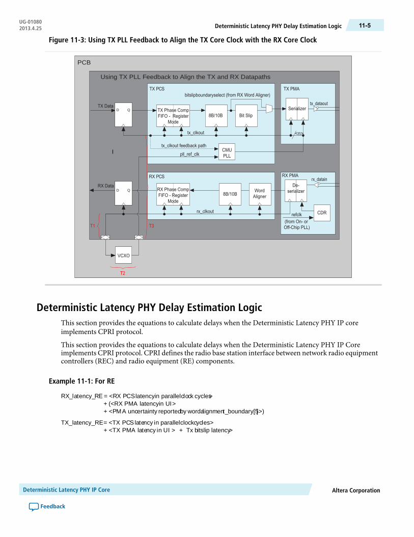
Figure 11-3: Using TX PLL Feedback to Align the TX Core Clock with the RX Core Clock
TX Data
RX Data
T3
T2
T1
bitslipboundaryselect (from RX Word Aligner)TX PMA
tx_dataoutD Q
D Q
Serializer
RX PMA
De-serializer
CMUPLL
VCXO
CDRrefclk(from On- orOff-Chip PLL)
<n>
8B/10B
rx_datainRX PCS
TX PCS
Using TX PLL Feedback to Align the TX and RX Datapaths
PCB
tx_clkout
pll_ref_clk
tx_clkout feedback path
rx_clkout
8B/10BWordAligner
Bit SlipTX Phase CompFIFO - Register
Mode
RX Phase CompFIFO - Register
Mode
Deterministic Latency PHY Delay Estimation LogicThis section provides the equations to calculate delays when the Deterministic Latency PHY IP coreimplements CPRI protocol.
This section provides the equations to calculate delays when the Deterministic Latency PHY IP Coreimplements CPRI protocol. CPRI defines the radio base station interface between network radio equipmentcontrollers (REC) and radio equipment (RE) components.
Example 11-1: For RE
RX_latency_RE = <RX PCSlatencyin parallelclock cycles>+ (<RX PMA latencyin UI>+ <PMA uncertainty reportedby wordalignment_boundary[5]>)
TX_latency_RE= <TX PCS latency in parallelclockcycles>+ <TX PMA latency in UI > Tx bitslip latency>+
Altera CorporationDeterministic Latency PHY IP Core
Feedback
11-5Deterministic Latency PHY Delay Estimation LogicUG-010802013.4.25

Example 11-2: For REC
For REC
RX_latency_REC = <RX PCS latency in parallel clock cycles>+ <RX PMA latency in UI> + < rx_clkoutphaseshift of tx_clkout>
TX_latency_REC= <TX PCSlatencyin parallelclockcycles>+ <TX PMA latency in UI>
Example 11-3: For Round Trip Delay
Launch_time(from TX pin s) =<clockarrival time>+ <data arrival time>
= <clockarrival time>+ <TX latency in REC> (tx bitslip=0)
= <tPD GPLL to CMU PLL - t feedback>+ ((<TX_latency in REC> × <tx_clkout_period>)+ tTX_tclock_output)
Arrival _time (at RX pins) = <latencytime in RE> - <RX latency timein REC>
= (<Round_trip_latency> × <tx_clkout_period>)– ((<RX_latency in REC> × <rx_clkout_period>)+ <tPDIO>RX_deser >+ <rx_clkout_phase_WRT_tx_clkout/360× rx_clkout_period>)
Total Delay = <Ar rival_time> – <Launch_time>
Example 11-4: Total Delay Uncertainty
Round trip delay estimates are subject to process, voltage, and temperature (PVT) variation.
tRXCLK_Phase_detector_uncertainty = 2 × max(<tGLL_phase_step>, <tCDR_to_GPLL_jitter>) + µtSU + µtH
tRound_trip_uncertaint y = <tRX_CLK_Phase_detector_uncertainty + tGPLL->CMU PLL_variation>+<tfeedback_variation> + <tTX_tco_variation > + <t IO->RXdeser_delay_variation >+ <tPLL_multicycle_jitter> + <toffset_uncertainty>
Table 11-2: TX PCS Total Latency
This table shows the total latency through the TX PCS in parallel clock cycles with the byte serializer/deserializerturned off. The TX compensation FIFO is in register mode.
Total TX Paral-lel Clock Cycles
Bitslip8B/10BSerializerTX Phase CompFIFO
PCS Datapath Width
Byte Serializer/Deserializer Turned Off
3.001.01.01.08 bits
3.001.01.01.016 bits
Byte Serializer/Deserializer Turned On
2.000.50.51.016 bits
Deterministic Latency PHY IP CoreAltera Corporation
Feedback
UG-01080Deterministic Latency PHY Delay Estimation Logic11-6 2013.4.25

Total TX Paral-lel Clock Cycles
Bitslip8B/10BSerializerTX Phase CompFIFO
PCS Datapath Width
2.000.50.51.032 bits
Table 11-3: RX PCS Total Latency
The RX compensation FIFO is in register mode. When the byte serializer/deserializer in turned on, the latencythrough is function depends on the location of the alignment pattern. When the alignment pattern is in theupper symbol, the delay is 0.5 cycles. When the alignment pattern is in the lower symbol, the delay is 1.0 cycles.
Total RX Par-allel Clock
Cycles
Word Aligner8B/10BDeserializerByte Order-ing
RX PhaseComp FIFO
PCS Datapath Width
Byte Serializer/Deserializer Turned Off
8.04.01.01.01.01.08 bits
9.05.01.01.01.01.016 bits
Byte Serializer/Deserializer Turned On
5.0 or 5.52.00.50.5 or 1.01.01.016 bits
5.5 or 6.02.50.50.5 or 1.01.01.032 bits
Table 11-4: PMA Datapath Total Latency
The numbers in this table are from simulation.TX PMA Latency in UIRX PMA Latency in UI
Device PCS to PMA Width 20bits
PCS to PMA Width 10bits
PCS to PMA Width 20bits
PCS to PMA Width 10bits
83534323Arria V
84542313Stratix V
There is a small discrepancy between simulation of the delays through the PMA serializer anddeserializer and hardware modeling of these delays.
Note:
Deterministic Latency PHY Device Family SupportThis section describes Deterministic Latency PHY IP core device support.
IP cores provide either final or preliminary support for target Altera device families. These terms have thefollowing definitions:
• Final support—Verified with final timing models for this device.• Preliminary support—Verified with preliminary timing models for this device.
Table 11-5: Device Family Support
SupportDevice Family
PreliminaryArria V devices
Altera CorporationDeterministic Latency PHY IP Core
Feedback
11-7Deterministic Latency PHY Device Family SupportUG-010802013.4.25

SupportDevice Family
PreliminaryArria V GZ devices
PreliminaryCyclone V devices
PreliminaryStratix V devices
No supportOther device families
Parameterizing the Deterministic Latency PHYThis section provides a list of steps on how to configure Deterministic Latency PHY using the MegaWizardPlug-In Manager.
1. For Which device family will you be using?, select Stratix V.2. Click Installed Plug-Ins > Interfaces > Transceiver PHY > Deterministic Latency PHY v12.1.3. Use the tabs on the MegaWizard Plug-In Manager to select the options required for the protocol.
a. Set the Deterministic Latency PHY general options parameters.b. Set the Deterministic Latency PHY additional options parameters.c. Set the Deterministic Latency PHY PLL reconfiguration parameters as required.d. Set the Deterministic Latency PHY additional options parameters as required.
4. Click Finish.Generates your customized Deterministic Latency PHY IP Core.
General Options Parameters for Deterministic Latency PHYThis section describes how to set basic parameters of your transceiver PHY for the Deterministic LatencyPHY IP core using the general options tab.
Use the General Options tab to set your basic device parameter settings.
Table 11-6: General Options
DescriptionValueName
Specifies the device family. Arria V, Cyclone V, and Stratix V areavailable.
Arria V, Cyclone V,Stratix V
Device family
You can select to transmit data, receive data, or both.Duplex, TX, RXMode of operation
The total number of lanes in each direction.1-32Number of lanes
Specifies the word size between the FPGA fabric and PCS. Referto Table 11-7 for the data rates supported at each word size.
8, 10, 16, 20, 32, 40FPGA fabrictransceiver interfacewidth
Specifies the datapath width between the transceiver PCS andPMA. A deserializer in the PMA receives serial input data fromtheRXbuffer using the high-speed recovered clock anddeserializesit using the low-speed parallel recovered clock.
10, 20PCS-PMA interfacewidth
Deterministic Latency PHY IP CoreAltera Corporation
Feedback
UG-01080Parameterizing the Deterministic Latency PHY11-8 2013.4.25

DescriptionValueName
Specifies the PLL type. TheCMUPLL has a larger frequency rangethan the ATX PLL. The ATX PLL is designed to improve jitterperformance and achieves lower channel-to-channel skew;however, it supports a narrower range of data rates and referenceclock frequencies. Another advantage of the ATX PLL is that itdoes not use a transceiver channel, while the CMU PLL does.Because theCMUPLL ismore versatile, it is specified as the defaultsetting.
CMU, ATXPLL type
If you select a data rate that is not supported by the configurationyou have specified, the MegaWizard displays a error message inthe message pane. Table 11-7 for sample the channel widths thatsupport these data rates.
Device DependentData rate
For systems that transmit and receive data at more than one datarate, select a base data rate that minimizes the number of PLLsrequired to generate the clocks for data transmission. TheRecommended Base Data Rate and Clock Divisors for CPRI tablelists the recommended Base data rates for various Data rates.
The available options are dynamically computed based on theData rate you specified as long as thoseBase data rates are withinthe frequency range of the PLL.
1 × Data rate
2 × Data rate
4 × Data rate
8 × Data rate
Base data rate
This is the reference clock for the PHY PLL. The available optionsare based on the Base data rate specified.
Data rate/20
Data rate/10
Data rate/8
Data rate/5
Data rate/4
Data rate/2.5
Data rate/2
Data rate/1.25
Data rate/1
Input clockfrequency
When On, the core uses TX PLL feedback to align the TX coreclock with the source to the TX PLL which is the RX recoveredclock. This configuration is shown in Using TX PLL Feedback toAlign the TX Core Clock with the RX Core Clock.
On/ OffEnable tx_clkoutfeedback path forTX PLL
The following table lists the available channel widths available at selected frequencies. The channel widthoptions are restricted by the following maximum FPGA-PCS fabric interface frequencies:
• Arria V devices—153.6 MHz• Cyclone V devices—153.6 MHz• Stratix V devices—221 MHz
Altera CorporationDeterministic Latency PHY IP Core
Feedback
11-9General Options Parameters for Deterministic Latency PHYUG-010802013.4.25

Table 11-7: Sample Channel Width Options for Supported Serial Data Rates
Channel Width (FPGA-PCS Fabric)Serial Data Rate
(Mbps)Double-WidthSingle-Width
32-Bit16-Bit16-Bit8-Bit
NoNoYesYes614.4
YesYesYesYes1228.8
YesYesYesNo2457.6
YesYesYesNo3072
YesNoNoNo4915.2
YesNoNoNo6144
Additional Options Parameters for Deterministic Latency PHYThis section describes the settings available on the Additional Options tab for the Deterministic LatencyPHY IP core.
DescriptionValueName
The word aligner restores word boundaries of received databased on a predefined alignment pattern. The word alignerautomatically performs an initial alignment to the specifiedwordpattern after reset deassertion. You can select 1 of the following2 modes: Deterministic latency state machine or Manual
Word alignment mode
Deterministic Latency PHY IP CoreAltera Corporation
Feedback
UG-01080Additional Options Parameters for Deterministic Latency PHY11-10 2013.4.25

DescriptionValueName
Deterministic latency statemachine–In thismode, theRXwordaligner automatically searches for the word alignment patternafter reset completes. After the word aligner detects the specifiedword alignment pattern, it sendsRX_CLKSLIP to the RXPMAdeserializer indicating the number of bits to slip to compensatefor the bits that were slipped to achieve word alignment. WhenRX_CLKSLIP has a non-zero value, the deserializer either skipsone serial bit or pauses the serial clock for one cycle. As a result,the period of the parallel clock could be extended by 1 unitinterval (UI) during the clock slip operation. This procedureavoids using the TX bit slipper to ensure constant round-tripdelay.
Deterministiclatency statemachine
Word alignment mode
In this mode, the specified word alignment pattern, which iscurrently forced to K28.5 (0011111010) is always placed in theleast significant byte (LSB) of a word with a fixed latency of 3cycles. User logic can assume the LSB placement. Alterarecommends the deterministic latency state machine mode fornew designs.
During the word alignment process, the parallel clock shifts thephase to align to the data. This phase shifting will be 2/10 cycles(20%) in 10 bit mode, 2/20 cycles (10%) in 20 bit mode, and 2/40cycles (5%) in 40 bit mode.
For double-width datapaths using deterministic latency statemachine mode, after the initial alignment following thedeassertion of reset, the Avalon-MM register big rx_enapatternalign (not available as a signal) must bereasserted to initiate another pattern alignment. Asserting rx_enapatternalign, may cause the extra shifting in the RXdatapath if rx_enablepatternalign is asserted while bitslipping is in progress; consequentlyrx_enapatternalignshould only be asserted under the following conditions:
• rx_syncstatus is asserted• rx_bitslipboundaryselectout changes from a
non-zero value to zero or 1
Manual–In thismode, the RXword aligner parses the incomingdata stream for a specific alignment character. After it identifiesthis pattern, it shifts the input stream to align the data and alsooutputs the number of bits slipped onbitslipboundaryselectout[4:0] for latencycompensation on the TX datapath. This mode is provided forbackwards compatibility with designs implemented in StratixIV and Arria II devices.
ManualWord alignment mode
Altera CorporationDeterministic Latency PHY IP Core
Feedback
11-11Additional Options Parameters for Deterministic Latency PHYUG-010802013.4.25

DescriptionValueName
TX bitslip is enabled whenever the word aligner is in Manualalignment mode. The TX bitslipper uses the value ofbitslipboundarselect[4:0] to compensate for bitsslipped on the RX datapath to achieve deterministic latency.
On/ OffTX bitslip
If you turn this option on, you can specify the run length whichis themaximum legal number of contiguous 0s or 1s. This optionalso creates the rx_rlv output signal which is asserted when arun length violation is detected.
On/ OffEnable run lengthviolation checking
Specifies the threshold for a run-length violation. Must be amultiple of 5.
5-160Run length
Enable this option to include the rx_patterndetect andrx_syncstatus ports.
On/ OffCreate optional wordaligner status ports
Enable this option to include the 8B/10B rx_runningdisp,rx_errdetect, and rx_disperr signals at the top level ofthe Deterministic Latency PHY IP Core.
On/ OffCreate optional 8B/10Bcontrol and status ports
Enable this option to include the 8B/10B rx_is_lockedtoref, rx_is_lockedtodata, and rx_signaldetect signals at the top level of the DeterministicLatency PHY IP Core.
On/ OffCreate PMA optionalstatus ports
This option is typically required if you are planning to importyour Deterministic Latency PHY IP Core into a Qsys system.
On/ OffAvalon data interfaces
When you turn this option On, the embedded reset controllerhandles reset of the TX and RX channels at power up. If youturn this option Off, you must design a reset controller thatmanages the following reset signals:tx_digitalreset,tx_analogreset,tx_cal_busy,rx_digitalreset,rx_analogreset, and rx_cal_busy. You may also use theTransceiver PHY Reset Controller to reset the transceivers. Formore information, refer to the Transceiver ReconfigurationController IP Core.
On/ OffEnable embedded resetcontroller
Related InformationTransceiver Architecture in Arria V Devices
Transceiver Architecture in Cyclone V Devices
Transceiver Architecture in Stratix V Devices
Transceiver Reconfiguration Controller IP Core Overview on page 16-1
PLL Reconfiguration Parameters for Deterministic Latency PHYThe section describes the PLL Reconfiguration options for the Deterministic Latency PHY IP core.
This table lists the PLL Reconfiguration options. For more information about transceiver reconfigurationregisters, refer to PLL Reconfiguration.
Deterministic Latency PHY IP CoreAltera Corporation
Feedback
UG-01080PLL Reconfiguration Parameters for Deterministic Latency PHY11-12 2013.4.25

Table 11-8: PLL Reconfiguration Options
DescriptionValueName
You must enable this option if you plan to reconfigure thePLLs in your design. This option is also required to simulatePLL reconfiguration.
On/OffAllow PLL/CDRReconfiguration
Specifies the number of TX PLLs required for this instanceof the Custom PHY. More than 1 PLL may be required ifyour design reconfigures channels to run at multiplefrequencies.
Device dependentNumber of TX PLLs
Specifies the number of input reference clocks. More thanone reference clock may be required if your designreconfigures channels to run at multiple frequencies.
1-5Number of reference clocks
Specifies the index for the TXPLL that should be instantiatedat startup. Logical index 0 corresponds to TX PLL0, and soon.
0-3Main TX PLL logical index
Specifies the index for the TX PLL input clock that shouldbe instantiated at startup. Logical index 0 corresponds toinput clock 0 and so on.
0-3Main TX PLL input clocksource
Specifies the index for the CDR PLL input clock that shouldbe instantiated at startup. Logical index 0 corresponds toinput clock 0 and so on.
0-4CDRPLL input clock source
TX PLL (0–3) (Refer to General Options for a detailed explanation of these parameters.)
Specifies the PLL type.CMUPLL Type
Specifies Base data rate.1 × Lane rate
2 × Lane rate
4 × Lane rate
Base data rate
Specifies the frequency of the PLL input reference clock. ThePLLmust generate an output frequency that equals theBasedata rate/2. You can use any Input clock frequency thatallows the PLLs to generate this output frequency.
VariableInput clock frequency
Specifies the index of the input clock for this TXPLL. Logicalindex 0 corresponds to input clock 0 and so on.
0-4Selected input clock source
Channel Interface
Altera CorporationDeterministic Latency PHY IP Core
Feedback
11-13PLL Reconfiguration Parameters for Deterministic Latency PHYUG-010802013.4.25
DescriptionValueName
Turn this option on to enable PLL and datapath dynamicreconfiguration. When you select this option, the width oftx_parallel_data and rx_parallel_data busesincreases in the following way:
• The rx_parallel_data bus is 64 bits per lane;however, only the low-order number of bits specified bythe FPGA fabric transceiver interface width contain validdata.
• The tx_parallel_databus is 44 bits per lane;however, only the low-order number of bits specified bythe FPGA fabric transceiver interface width contain validdata for each lane.
On/OffEnable channel interface
Related InformationTransceiver Reconfiguration Controller PLL Reconfiguration on page 16-24
Deterministic Latency PHY Analog ParametersThis section provides links to describe analog parameters for the Deterministic Latency PHY IP core.
The following links provide information to specify the analog options for your device:
Related InformationAnalog Settings for Arria V Devices on page 19-2
Analog Settings for Arria V GZ Devices on page 19-9
Analog Settings for Cyclone V Devices on page 19-18
Analog Settings for Stratix V Devices on page 19-25
Interfaces for Deterministic Latency PHYThis section describes the top-level signals of the Deterministic Latency PHY IP Core.
The following figure illustrates the top-level signals of theDeterministic Latency PHY IPCore. The variablesin the figure represent the following parameters:
• <n>—The number of lanes• <w>—The width of the FPGA fabric to transceiver interface per lane• <s>— The symbol size• <p>—The number of PLLs
Deterministic Latency PHY IP CoreAltera Corporation
Feedback
UG-01080Deterministic Latency PHY Analog Parameters11-14 2013.4.25
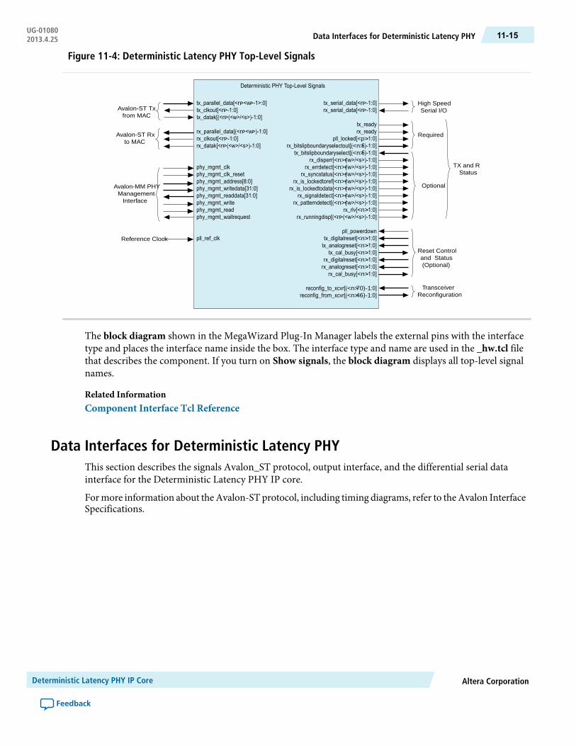
Figure 11-4: Deterministic Latency PHY Top-Level Signals
tx_parallel_data[<n><w>-1>:0]tx_clkout[<n>-1:0]tx_datak[(<n>(<w>/<s>)-1:0]
rx_parallel_data[(<n><w>)-1:0]rx_clkout[<n>-1:0]rx_datak[<n>(<w>/<s>)-1:0]
phy_mgmt_clkphy_mgmt_clk_resetphy_mgmt_address[8:0]phy_mgmt_writedata[31:0]phy_mgmt_readdata[31:0]phy_mgmt_writephy_mgmt_readphy_mgmt_waitrequest
pll_ref_clk
Deterministic PHY Top-Level Signals
tx_serial_data[<n>-1:0]rx_serial_data[<n>-1:0]
tx_readyrx_ready
pll_locked[<p>-1:0]rx_bitslipboundaryselectout[(<n>5)-1:0]
tx_bitslipboundaryselect[(<n>5)-1:0]rx_disperr[<n>(<w>/<s>)-1:0]
rx_errdetect[<n>(<w>/<s>)-1:0]rx_syncstatus[<n>(<w>/<s>)-1:0]
rx_is_lockedtoref[<n>(<w>/<s>)-1:0]rx_is_lockedtodata[<n>(<w>/<s>)-1:0]
rx_signaldetect[<n>(<w>/<s>)-1:0]rx_patterndetect[(<n>(<w>/<s>)-1:0]
rx_rlv[<n>-1:0]rx_runningdisp[(<n>(<w>/<s>)-1:0]
pll_powerdowntx_digitalreset[<n>-1:0]tx_analogreset[<n>-1:0]
tx_cal_busy[<n>-1:0]rx_digitalreset[<n>-1:0]rx_analogreset[<n>-1:0]
rx_cal_busy[<n>-1:0]
reconfig_to_xcvr[(<n>70)-1:0]reconfig_from_xcvr[(<n>46)-1:0]
Avalon-ST Txfrom MAC
High SpeedSerial I/O
Avalon-MM PHYManagement
Interface
Reference Clock
Reset Controland Status(Optional)
Optional
Required
TX and RXStatus
Avalon-ST Rxto MAC
TransceiverReconfiguration
The block diagram shown in the MegaWizard Plug-In Manager labels the external pins with the interfacetype and places the interface name inside the box. The interface type and name are used in the _hw.tcl filethat describes the component. If you turn on Show signals, the block diagram displays all top-level signalnames.
Related InformationComponent Interface Tcl Reference
Data Interfaces for Deterministic Latency PHYThis section describes the signals Avalon_ST protocol, output interface, and the differential serial datainterface for the Deterministic Latency PHY IP core.
Formore information about theAvalon-ST protocol, including timing diagrams, refer to theAvalon InterfaceSpecifications.
Altera CorporationDeterministic Latency PHY IP Core
Feedback
11-15Data Interfaces for Deterministic Latency PHYUG-010802013.4.25

Table 11-9: Avalon-ST TX Interface
The following table describes the signals in the Avalon-ST input interface. These signals are driven from theMAC to the PCS. This is an Avalon sink interface.
DescriptionDirectionSignal Name
This is TX parallel data driven from the MAC. The readylatency on this interface is 0, so that the PHY must be ableto accept data as soon as it comes out of reset. Refer to fordefinitions of the control and status signals with 8B/10Bencoding enabled and disabled. Refer to Table 11-11 forthe signals that correspond to data, control, and statussignals.
Inputtx_parallel_data[(<n><w>)-1:0]
This is the clock for TX parallel data, control, and statussignals.
Outputtx_clkout[<n>-:0]
Data and control indicator for the received data. When 0,indicates that tx_parallel_data is data, when 1,indicates that tx_parallel_data is control.
Inputtx_datak[(<n><d>/<s>)-1:0]
Table 11-10: Signal Definitions for tx_parallel_data with and without 8B/10B Encoding
The following table shows the signals within tx_parallel_data that correspond to data, control, and status signals.DescriptionTX Data Word
Signal Definitions with 8B/10B Enabled
TX data bustx_parallel_data[7:0]
TX data control charactertx_parallel_data[8]
Force disparity, validates disparity field.tx_parallel_data[9]
Specifies the current disparity as follows:
• 1'b0 = positive• 1'b1 = negative
tx_parallel_data[10]
Signal Definitions with 8B/10B Disabled
TX data bustx_parallel_data[9:0]
Unusedtx_parallel_data[10]
Deterministic Latency PHY IP CoreAltera Corporation
Feedback
UG-01080Data Interfaces for Deterministic Latency PHY11-16 2013.4.25
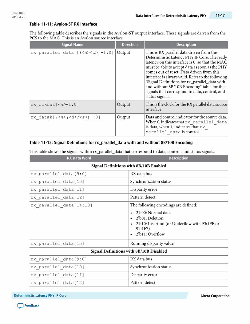
Table 11-11: Avalon-ST RX Interface
The following table describes the signals in the Avalon-ST output interface. These signals are driven from thePCS to the MAC. This is an Avalon source interface.
DescriptionDirectionSignal Name
This is RX parallel data driven from theDeterministic LatencyPHY IPCore. The readylatency on this interface is 0, so that the MACmust be able to accept data as soon as the PHYcomes out of reset. Data driven from thisinterface is always valid. Refer to the following"Signal Definitions for rx_parallel_data withand without 8B/10B Encoding" table for thesignals that correspond to data, control, andstatus signals.
Outputrx_parallel_data [(<n><d>)-1:0]
This is the clock for the RXparallel data sourceinterface.
Outputrx_clkout[<n>-1:0]
Data and control indicator for the source data.When0, indicates thatrx_parallel_datais data, when 1, indicates that rx_parallel_data is control.
Outputrx_datak[(<n>(<d>/<s>)-:0]
Table 11-12: Signal Definitions for rx_parallel_data with and without 8B/10B Encoding
This table shows the signals within rx_parallel_data that correspond to data, control, and status signals.DescriptionRX Data Word
Signal Definitions with 8B/10B Enabled
RX data busrx_parallel_data[9:0]
Synchronization statusrx_parallel_data[10]
Disparity errorrx_parallel_data[11]
Pattern detectrx_parallel_data[12]
The following encodings are defined:
• 2’b00: Normal data• 2’b01: Deletion• 2’b10: Insertion (or Underflow with 9’h1FE or
9’h1F7)• 2’b11: Overflow
rx_parallel_data[14:13]
Running disparity valuerx_parallel_data[15]
Signal Definitions with 8B/10B Disabled
RX data busrx_parallel_data[9:0]
Synchronization statusrx_parallel_data[10]
Disparity errorrx_parallel_data[11]
Pattern detectrx_parallel_data[12]
Altera CorporationDeterministic Latency PHY IP Core
Feedback
11-17Data Interfaces for Deterministic Latency PHYUG-010802013.4.25

DescriptionRX Data Word
The following encodings are defined:
• 2’b00: Normal data• 2’b01: Deletion• 2’b10: Insertion (or Underflow with 9’h1FE or
9’h1F7)• 2’b11: Overflow
rx_parallel_data[14:13]
Running disparity valuerx_parallel_data[15]
Table 11-13: Serial Interface and Status Signals
This table describes the differential serial data interface and the status signals for the transceiver serial datainterface. <n> is the number of lanes.
Signal NameDirectionSignal Name
Receiver differential serial input data.Inputrx_serial_data[<n>-:0]
Transmitter differential serial output data.Outputtx_serial_data[<n>-:0]
Related InformationAvalon Interface Specifications
Clock Interface for Deterministic Latency PHYThis section describes the clocks for the Deterministic Latency PHY IP core.
The following table describes clocks for the Deterministic Latency PHY. The input reference clock,pll_ref_clk, drives a PLL inside the PHY-layer block, and a PLL output clock, rx_clkout is used forall data, command, and status inputs and outputs.
Table 11-14: Clock Signals
DescriptionDirectionSignal Name
Reference clock for the PHY PLLs.Frequency range is 60-700 MHz.
Inputpll_ref_clk
Optional TX and RX Status Interface for Deterministic Latency PHYThis section describes the optional TX and RX status interface settings for the Deterministic Latency PHYIP core.
Table 11-15: Serial Interface and Status Signals
Signal NameDirectionSignal Name
When asserted, indicates that the TX interfacehas exited the reset state and is ready to transmit.
Outputtx_ready
Deterministic Latency PHY IP CoreAltera Corporation
Feedback
UG-01080Clock Interface for Deterministic Latency PHY11-18 2013.4.25

Signal NameDirectionSignal Name
When asserted, indicates that the RX interfacehas exited the reset state and is ready to receive.
Outputrx_ready
When asserted, indicates that the PLL is lockedto the input reference clock.
Outputpll_locked [<p>-1:0]
Specifies the number of bits slipped to achieveword alignment. In 3G (10-bit)mode, the outputis the number of bits slipped. If no bits wereslipped, the output is 0. In 6G (20-bit) mode, theoutput is (19 - the number of bits slipped). If nobits were slipped, the output is 19. The defaultvalue of rx_bitslipboundaryselectout[4:0]before alignment is achieved is 5'b01111 in 3Gmode and 5'b11111 in 6G mode.
Outputrx_bitslipboundaryselectout[(<n>5)-1:0]
Optional Status Signals
This signal is used for bit slip word alignmentmode. It selects the number of bits that the TXblock must slip to achieve a deterministiclatency.
Inputtx_bitslipboundaryselect[(<n> 5)-1:0]
When asserted, indicates that the received 10-bitcode or data group has a disparity error.
Outputrx_disperr [(<n><d>/<s>)-1:0]
When asserted, indicates that a received 10-bitcode group has an 8B/10B code violation ordisparity error.
Outputrx_errdetect [(<n><d>/<s>)-1:0]
Indicates presence or absence of synchronizationon the RX interface. Assertedwhenword aligneridentifies the word alignment pattern orsynchronization code groups in the received datastream. This signal is optional.
Outputrx_syncstatus [(<n><d>/<s>)-1:0]
Assertedwhen the receiver CDR is locked to theinput reference clock. This signal isasynchronous. This signal is optional.
Outputrx_is_lockedtoref [(<n>(<d>/<s>)-1:0]
When asserted, the receiver CDR is in tolock-to-data mode. When deasserted, thereceiver CDR lock mode depends on the rx_locktorefclk signal level. This signal isoptional.
Outputrx_is_lockedtodata [(<n><d>/<s>)-1:0]
When asserted, indicates that the programmedword alignment pattern has been detected in thecurrent word boundary.
Outputrx_patterndetect [(<n>(<d>/<s>)-1:0]
Altera CorporationDeterministic Latency PHY IP Core
Feedback
11-19Optional TX and RX Status Interface for Deterministic Latency PHYUG-010802013.4.25
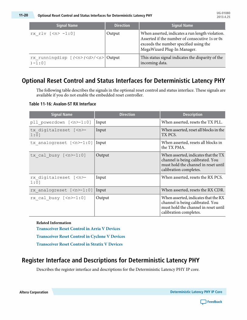
Signal NameDirectionSignal Name
When asserted, indicates a run length violation.Asserted if the number of consecutive 1s or 0sexceeds the number specified using theMegaWizard Plug-In Manager.
Outputrx_rlv [<n> -1:0]
This status signal indicates the disparity of theincoming data.
Outputrx_runningdisp [(<n>(<d>/<s>)-1:0]
Optional Reset Control and Status Interfaces for Deterministic Latency PHYThe following table describes the signals in the optional reset control and status interface. These signals areavailable if you do not enable the embedded reset controller.
Table 11-16: Avalon-ST RX Interface
DescriptionDirectionSignal Name
When asserted, resets the TX PLL.Inputpll_powerdown [<n>-1:0]
When asserted, reset all blocks in theTX PCS.
Inputtx_digitalreset [<n>-1:0]
When asserted, resets all blocks inthe TX PMA.
Inputtx_analogreset [<n>-1:0]
When asserted, indicates that theTXchannel is being calibrated. Youmust hold the channel in reset untilcalibration completes.
Outputtx_cal_busy [<n>-1:0]
When asserted, resets the RX PCS.Inputrx_digitalreset [<n>-1:0]
When asserted, resets the RX CDR.Inputrx_analogreset [<n>-1:0]
When asserted, indicates that theRXchannel is being calibrated. Youmust hold the channel in reset untilcalibration completes.
Outputrx_cal_busy [<n>-1:0]
Related InformationTransceiver Reset Control in Arria V Devices
Transceiver Reset Control in Cyclone V Devices
Transceiver Reset Control in Stratix V Devices
Register Interface and Descriptions for Deterministic Latency PHYDescribes the register interface and descriptions for the Deterministic Latency PHY IP core.
Deterministic Latency PHY IP CoreAltera Corporation
Feedback
UG-01080Optional Reset Control and Status Interfaces for Deterministic Latency PHY11-20 2013.4.25

The Avalon-MM PHY management interface provides access to the Deterministic Latency PHY PCS andPMA registers that control the TX and RX channels, the PMA powerdown and PLL registers, and loopbackmodes.
The following figure illustrates the role of the PHY Management module in the Deterministic Latency PHY.
Figure 11-5: Deterministic Latency PHY IP Core
SystemInterconnect
FabricSystem
InterconnectFabric
Deterministic PHY PCS and PMA
Deterministic PHY IP Core
Resets
Status
ControlS Avalon-MMControl
S Avalon-MMStatus
ResetController
PLL
Reset
Clocks Clocks
toTransceiver
ReconfigurationController
toEmbeddedController
Tx Data Tx Parallel Data
Rx Data Rx Parallel Data
MAvalon-MM
PHYMgmt
S
Rx Serial Data & Status
Reconfig to and from Transceiver
Tx Serial Data
Table 11-17: Avalon-MM PHY Management Interface
DescriptionDirectionSignal Name
Avalon-MM clock input. There is no frequency restriction forStratix V devices; however, if you plan to use the same clock forthe PHYmanagement interface and transceiver reconfiguration,you must restrict the frequency range of phy_mgmt_clk to100-150 MHz to meet the specification for the transceiverreconfiguration clock.
Inputphy_mgmt_clk
Global reset signal. This signal is active high and level sensitive.Inputphy_mgmt_clk_reset
9-bit Avalon-MM address.Inputphy_mgmt_address[8:0]
Input data.Inputphy_mgmt_writedata[31:0]
Output data.Outputphy_mgmt_readdata[31:0]
Write signal.Inputphy_mgmt_write
Altera CorporationDeterministic Latency PHY IP Core
Feedback
11-21Register Interface and Descriptions for Deterministic Latency PHYUG-010802013.4.25
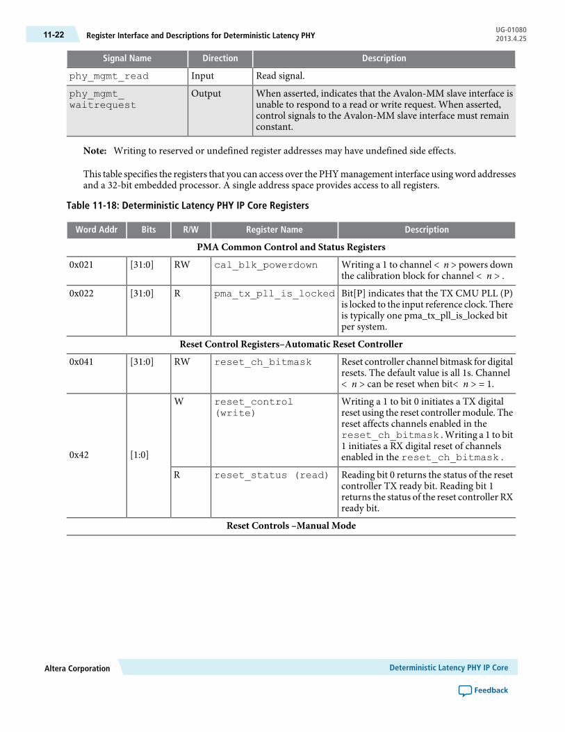
DescriptionDirectionSignal Name
Read signal.Inputphy_mgmt_read
When asserted, indicates that the Avalon-MM slave interface isunable to respond to a read or write request. When asserted,control signals to the Avalon-MM slave interface must remainconstant.
Outputphy_mgmt_waitrequest
Writing to reserved or undefined register addresses may have undefined side effects.Note:
This table specifies the registers that you can access over the PHYmanagement interface usingword addressesand a 32-bit embedded processor. A single address space provides access to all registers.
Table 11-18: Deterministic Latency PHY IP Core Registers
DescriptionRegister NameR/WBitsWord Addr
PMA Common Control and Status Registers
Writing a 1 to channel < n > powers downthe calibration block for channel < n > .
cal_blk_powerdownRW[31:0]0x021
Bit[P] indicates that the TX CMU PLL (P)is locked to the input reference clock. Thereis typically one pma_tx_pll_is_locked bitper system.
pma_tx_pll_is_lockedR[31:0]0x022
Reset Control Registers–Automatic Reset Controller
Reset controller channel bitmask for digitalresets. The default value is all 1s. Channel< n > can be reset when bit< n > = 1.
reset_ch_bitmaskRW[31:0]0x041
Writing a 1 to bit 0 initiates a TX digitalreset using the reset controllermodule. Thereset affects channels enabled in thereset_ch_bitmask . Writing a 1 to bit1 initiates a RX digital reset of channelsenabled in the reset_ch_bitmask .
reset_control(write)
W
[1:0]0x42
Reading bit 0 returns the status of the resetcontroller TX ready bit. Reading bit 1returns the status of the reset controller RXready bit.
reset_status (read)R
Reset Controls –Manual Mode
Deterministic Latency PHY IP CoreAltera Corporation
Feedback
UG-01080Register Interface and Descriptions for Deterministic Latency PHY11-22 2013.4.25

DescriptionRegister NameR/WBitsWord Addr
You canuse thereset_fine_controlregister to create your own reset sequence.In manual mode, only the TX reset occursautomatically at power on and when thephy_mgmt_clk_reset is asserted.When pma_rx_setlocktodata orpma_rx_setlocktodata is set, thetransceiver PHY is placed inmanualmode.
reset_fine_controlRW[31:0]
0x044
It is safe to write 0s to reserved bits.ReservedRW[31:4,0]
Writing a 1 causes the internal RX digitalreset signal to be asserted, resetting the RXdigital channels enabled in reset_ch_bitmask . You must write a 0 to clear thereset condition.
reset_rx_digitalRW[3]
Writing a 1 causes the internal RX analogreset signal to be asserted, resetting the RXanalog logic of all channels enabled inreset_ch_bitmask . You must writea 0 to clear the reset condition.
reset_rx_analogRW[2]
Writing a 1 causes the internal TX digitalreset signal to be asserted, resetting allchannels enabled in reset_ch_bitmask . You must write a 0 to clear thereset condition.
reset_tx_digitalRW[1]
PMA Control and Status Registers
Writing a 1 to channel < n > puts channel< n > in serial loopback mode. Forinformation about pre- or post-CDR serialloopbackmodes, refer to LoopbackModes.
phy _ serial _loopback
RW[31:0]0x061
When set, programs the RX CDR PLL tolock to the incoming data. Bit < n>corresponds to channel < n>.
pma_rx_set_locktodata
RW[31:0]0x064
When set, programs the RX CDR PLL tolock to the reference clock. Bit < n>corresponds to channel < n>.
pma_rx_set_locktorefRW[31:0]0x065
When asserted, indicates that the RX CDRPLL is locked to the RX data, and that theRX CDR has changed from LTR to LTDmode. Bit <n> corresponds to channel <n>.
pma_rx_is_lockedtodata
RO[31:0]0x066
When asserted, indicates that the RX CDRPLL is locked to the reference clock. Bit <n> corresponds to channel < n>.
pma_rx_is_lockedtoref
RO[31:0]0x067
PCS
Altera CorporationDeterministic Latency PHY IP Core
Feedback
11-23Register Interface and Descriptions for Deterministic Latency PHYUG-010802013.4.25

DescriptionRegister NameR/WBitsWord Addr
Specifies lane or group number for indirectaddressing, which is used for all PCScontrol and status registers. For variantsthat stripe data across multiple lanes, thisis the logical group number. Fornon-bonded applications, this is the logicallane number.
Lane or group numberRW[31:0]0x080
Reserved.pcs8g_rx_statusR[31:6]
0x081This is an output from the bit slip wordaligner which shows the number of bitsslipped. From block: Word aligner.
rx_bitslipboundaryselectout
R[5:1]
-Reserved.R[0]
Reserved.pcs8g_tx_statusR[31:1]0x082
-ReservedRW[0]
Reserved.pcs8g_tx_controlRW[31:6]
0x083
Sets the number of bits that the TX bitslipper needs to slip. To block: Wordaligner.
tx_bitslipboundary_select
RW[5:1]
When set, the TX interface inverts thepolarity of the TX data. To block: 8B/10Bencoder.
tx_invpolarityRW[0]
-Reserved.RW[31:1]
0x084 When set, the RX channels inverts thepolarity of the received data. To block:8B/10B decoder.
rx_invpolarityRW[0]
Reserved.pcs8g_rx_wa_controlRW[31:4]
0x085
Every time this register transitions from 0to 1, the RX data slips a single bit.Toblock:Word aligner.
rx_bitslipRW[3]
When set, enables byte reversal on the RXinterface. To block: Byte deserializer RXPhase Comp FIFO.
rx_bytereversal_enable
RW[2]
When set, enables bit reversal on the RXinterface. To block: Word aligner.
rx_bitreversal_enable
RW[1]
When set inmanual word alignmentmode,the word alignment logic begins operationwhen this bit is set.Toblock:Word aligner.
rx_enapatternalignRW[0]
Deterministic Latency PHY IP CoreAltera Corporation
Feedback
UG-01080Register Interface and Descriptions for Deterministic Latency PHY11-24 2013.4.25

Related InformationLoopback Modes on page 16-50
Dynamic Reconfiguration for Deterministic Latency PHYDynamic reconfiguration compensates for circuit variations due to process, voltage, and temperature (PVT).
These process variations result in analog voltages that can be offset from required ranges. The calibrationperformed by the dynamic reconfiguration interface compensates for variations due to PVT.
Each channel and each TXPLL has a separate dynamic reconfiguration interfaces. TheMegaWizard Plug-InManager provides informational messages on the connectivity of these interfaces. The following exampleshows the messages for a single duplex channel.
Although you must initially create a separate reconfiguration interface for each channel and TX PLL in yourdesign, when theQuartus II software compiles your design, it reduces the number of reconfiguration interfacesby merging reconfiguration interfaces. The synthesized design typically includes a reconfiguration interfacefor at least three channels because three channels share an Avalon-MM slave interface which connects tothe Transceiver Reconfiguration Controller IP Core. Conversely, you cannot connect the three channelsthat share an Avalon-MM interface to different Transceiver Reconfiguration Controller IP Cores. Doing socauses a Fitter error. For more information, refer to Transceiver Reconfiguration Controller to PHY IPConnectivity.
Example 11-5: Information Messages for the Transceiver Reconfiguration Interface
PHY IP will require 2 reconfiguration interfaces forconnection to the external reconfiguration controller.
Reconfiguration interface offset 0 is connected to thetransceiver channel.
Reconfiguration interface offset 1 is connected to thetransmit PLL.
Table 11-19: Reconfiguration Interface
This table lists the signals in the reconfiguration interface. This interface uses the Avalon-MMPHYManagementinterface clock.
DescriptionDirectionSignal Name
Reconfiguration signals from the TransceiverReconfiguration Controller. <n> grows linearlywith the number of reconfiguration interfaces.
Inputreconfig_to_xcvr [(<n>70)-1:0]
Reconfiguration signals to the TransceiverReconfiguration Controller. <n> grows linearlywith the number of reconfiguration interfaces.
Outputreconfig_from_xcvr [(<n>46)-1:0]
Altera CorporationDeterministic Latency PHY IP Core
Feedback
11-25Dynamic Reconfiguration for Deterministic Latency PHYUG-010802013.4.25

Related InformationTransceiver Reconfiguration Controller to PHY IP Connectivity on page 16-48
Channel Placement and Utilization for Deterministic Latency PHYThis section describes the channel placement utilization restrictions for the Deterministic Latency PHY IPcore.
The Deterministic Latency PHY IP Core has the following restriction on channel placement:
• Channels 0–2 in transceiver banks GXB_L0 and GSB_R0 of Arria V devices are not available fordeterministic latency protocols.
The following figure shows the placement of transceiver banks in Arria V devices and indicates the channelsthat are not available.
Figure 11-6: Channel Placement and Available Channels in Arria V Devices
GXB_R0
GXB_R1
GXB_L0
GXB_L1
GXB_R2GXB_L2
Devices Available
Number of Channels Per Bank
Transceiver Bank Names
5AGXB5KF405AGXB7KF40
5AGXA5HF355AGXA7HF355AGXB1HF355AGXB1HF405AGXB3HF355AGXB3HF405AGXB5HF355AGXB7HF35
5AGXA1EF315AGXA3EF31
PC
IeH
ard
IP
PC
IeH
ard
IP
Ch 5Ch 4Ch 3Ch 2Ch 1Ch 0 Ch 0
Ch 1Ch 2Ch 3Ch 4Ch 5
Ch 5Ch 4Ch 3Ch 2Ch 1Ch 0 Ch 0
Ch 1Ch 2Ch 3Ch 4Ch 5
Ch 5Ch 4Ch 3Ch 2Ch 1Ch 0 Ch 0
Ch 1Ch 2Ch 3Ch 4Ch 5
Not Available forDeterministic
Protocols
Not Available forDeterministic
Protocols
Simulation Files and Example Testbench for Deterministic Latency PHYThis section describes simulation file requirements for the Deterministic Latency PHY IP core.
Refer to Running a Simulation Testbench for a description of the directories and files that the Quartus IIsoftware creates automatically when you generate your Deterministic Latency PHY IP Core.
Related InformationRunning a Simulation Testbench
Deterministic Latency PHY IP CoreAltera Corporation
Feedback
UG-01080Channel Placement and Utilization for Deterministic Latency PHY11-26 2013.4.25

12Stratix V Transceiver Native PHY IP Core
2013.4.25UG-01080 Subscribe Feedback
The Stratix V Transceiver Native PHY IP Core provides direct access to all control and status signals of thetransceiver channels. Unlike protocol-specific PHY IP Cores, the Native PHY IP Core does not include anAvalonMemory-Mapped (Avalon-MM) interface. Instead, it exposes all signals directly as ports. The StratixV Transceiver Native PHY IP Core provides the following three datapaths:
• Standard PCS• 10G PCS• PMA Direct
You can enable the Standard PCS, the 10G PCS, or both if your design uses the Transceiver ReconfigurationController to change dynamically between the two PCS datapaths. The transceiver PHY does not includean embedded reset controller. You can either design custom reset logic or incorporate Altera’s “TransceiverPHY Reset Controller IP Core” to implement reset functionality. In PMA Direct mode, the Native PHYprovides direct access to the PMA from the FPGA fabric; consequently, the latency for transmitted andreceived data is very low. However, you must implement any PCS function that your design requires in theFPGA fabric.
The following figure illustrates the use of the Stratix V Transceiver Native PHY IP Core. As this figureillustrates, TX PLL and clock data recovery (CDR) reference clocks from the pins of the device are input tothe PLLmodule andCDR logic.When enabled, the 10Gor Standard PCS drives TXparallel data and receivesRX parallel data. When neither PCS is enabled the Native PHY operates in PMA Direct mode.
ISO9001:2008Registered
© 2013 Altera Corporation. All rights reserved. ALTERA, ARRIA, CYCLONE, HARDCOPY, MAX, MEGACORE, NIOS, QUARTUS and STRATIXwords and logos are trademarks of Altera Corporation and registered in the U.S. Patent and Trademark Office and in other countries. All other wordsand logos identified as trademarks or service marks are the property of their respective holders as described at www.altera.com/common/legal.html.Altera warrants performance of its semiconductor products to current specifications in accordance with Altera's standard warranty, but reserves theright to make changes to any products and services at any time without notice. Altera assumes no responsibility or liability arising out of the applicationor use of any information, product, or service described herein except as expressly agreed to in writing by Altera. Altera customers are advised toobtain the latest version of device specifications before relying on any published information and before placing orders for products or services.
www.altera.com
101 Innovation Drive, San Jose, CA 95134

Figure 12-1: Stratix V Native Transceiver PHY IP Core
PLLsPMA
altera_xcvr_native_<dev>Transceiver Native PHY
TransceiverReconfiguration
Controller
Reconfiguration to XCVR
Reconfiguration from XCVR
TX and RX Resets
Calilbration BusyPLL and RX Locked
RX PCS Parallel Data
TX PCS Parallel Data
CDR Reference Clock
(when neither PCS is enabled)
TX PLL Reference ClockSerializer/Clock
GenerationBlock
RX Serial Data
toFPGA fabric
TransceiverPHY ResetController
TX PMA Parallel DataRX PMA Parallel Data
TX Serial DataSerializer
Deserializer
StandardPCS
(optional)
10G PCS(optional)
In a typical design, the separately instantiated Transceiver PHYReset Controller drives reset signals toNativePHY and receives calibration and locked status signal from theNative PHY. TheNative PHY reconfigurationbuses connect the external TransceiverReconfigurationController for calibration anddynamic reconfigurationof the PLLs.
You specify the initial configuration when you parameterize the IP core. The Transceiver Native PHY IPCore connects to the “Transceiver Reconfiguration Controller IP Core” to dynamically change referenceclocks and PLL connectivity at runtime.
Device Family Support for Stratix V Native PHYThis section describes the device family support available in the Stratix V native PHY.
IP cores provide either final or preliminary support for target Altera device families. These terms have thefollowing definitions:
• Final support—Verified with final timing models for this device.• Preliminary support—Verified with preliminary timing models for this device.
Table 12-1: Device Family Support
This tables lists the level of support offered by the Stratix V Transceiver Native PHY IP Core for Altera devicefamilies.
SupportDevice Family
PreliminaryStratix V devices
No supportOther device families
Stratix V Transceiver Native PHY IP CoreAltera Corporation
Feedback
UG-01080Device Family Support for Stratix V Native PHY12-2 2013.4.25

Performance and Resource Utilization for Stratix V Native PHYThis section describes the performance resource utilization for Stratix V native PHY.
Because the 10G PCS, Standard PCS, and PMA are implemented in hard logic, the Stratix V Native PHY IPCore uses less than 1% of the available ALMs, memory, primary and secondary logic registers.
Parameter PresetsPresets allow you to specify a group of parameters to implement a particular protocol or application.
If you apply a preset, the parameters with specific required values are set for you. When applied, the presetis in boldface and remains as such unless you change some of the preset parameters. Selecting a preset doesnot prevent you from changing any parameter tomeet the requirements of your design. The following figureillustrates the Preset panel and form to create custom presets.
Figure 12-2: Preset Panel and Form To Create Custom Presets
Parameterizing the Stratix V Native PHYThis section provides a list of instructions on how to configure the Stratix V native PHY IP core using theMegaWizard.
Complete the following steps to configure the Stratix V Native PHY IP Core in the MegaWizard Plug-InManager:
1. For Which device family will you be using? select Stratix V from the list.2. Click Installed Plug-Ins > Interfaces > Transceiver PHY > Stratix V Native PHY v12.1.3. Use the tabs on the MegaWizard Plug-In Manager to select the options required for the protocol.4. Click Finish.
Generates your customized Stratix V Native PHY IP Core.
Altera CorporationStratix V Transceiver Native PHY IP Core
Feedback
12-3Performance and Resource Utilization for Stratix V Native PHYUG-010802013.4.25
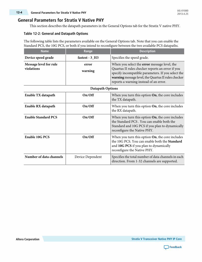
General Parameters for Stratix V Native PHYThis section describes the datapath parameters in the General Options tab for the Stratix V native PHY.
Table 12-2: General and Datapath Options
The following table lists the parameters available on the General Options tab. Note that you can enable theStandard PCS, the 10G PCS, or both if you intend to reconfigure between the two available PCS datapaths.
DescriptionRangeName
Specifies the speed grade.fastest - 3_H3Device speed grade
When you select the error message level, theQuartus II rules checker reports an error if youspecify incompatible parameters. If you select thewarningmessage level, theQuartus II rules checkerreports a warning instead of an error.
error
warning
Message level for ruleviolations
Datapath Options
When you turn this option On, the core includesthe TX datapath.
On/OffEnable TX datapath
When you turn this option On, the core includesthe RX datapath.
On/OffEnable RX datapath
When you turn this option On, the core includesthe Standard PCS . You can enable both theStandard and 10G PCS if you plan to dynamicallyreconfigure the Native PHY.
On/OffEnable Standard PCS
When you turn this option On, the core includesthe 10G PCS. You can enable both the Standardand 10G PCS if you plan to dynamicallyreconfigure the Native PHY.
On/OffEnable 10G PCS
Specifies the total number of data channels in eachdirection. From 1-32 channels are supported.
Device DependentNumber of data channels
Stratix V Transceiver Native PHY IP CoreAltera Corporation
Feedback
UG-01080General Parameters for Stratix V Native PHY12-4 2013.4.25
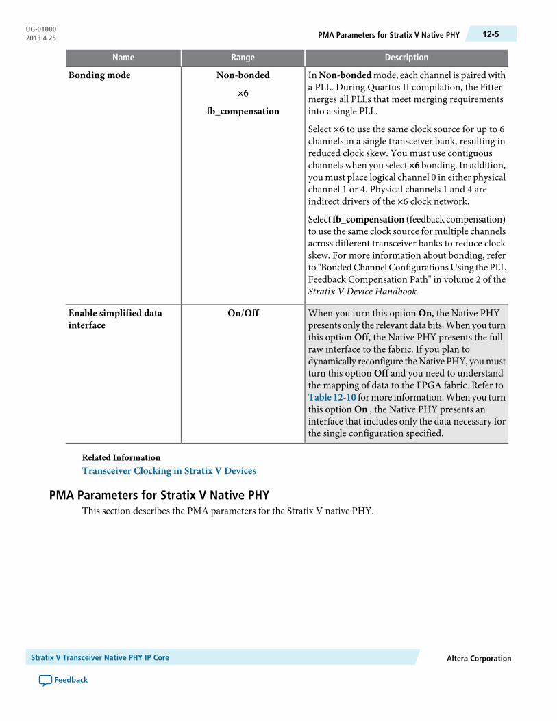
DescriptionRangeName
InNon-bondedmode, each channel is pairedwitha PLL. During Quartus II compilation, the Fittermerges all PLLs that meet merging requirementsinto a single PLL.
Select ×6 to use the same clock source for up to 6channels in a single transceiver bank, resulting inreduced clock skew. You must use contiguouschannels when you select×6 bonding. In addition,you must place logical channel 0 in either physicalchannel 1 or 4. Physical channels 1 and 4 areindirect drivers of the ×6 clock network.
Select fb_compensation (feedback compensation)to use the same clock source for multiple channelsacross different transceiver banks to reduce clockskew. For more information about bonding, referto "BondedChannel ConfigurationsUsing the PLLFeedback Compensation Path" in volume 2 of theStratix V Device Handbook.
Non-bonded
×6
fb_compensation
Bonding mode
When you turn this option On, the Native PHYpresents only the relevant data bits.When you turnthis option Off, the Native PHY presents the fullraw interface to the fabric. If you plan todynamically reconfigure theNative PHY, youmustturn this option Off and you need to understandthe mapping of data to the FPGA fabric. Refer toTable 12-10 formore information.When you turnthis option On , the Native PHY presents aninterface that includes only the data necessary forthe single configuration specified.
On/OffEnable simplified datainterface
Related InformationTransceiver Clocking in Stratix V Devices
PMA Parameters for Stratix V Native PHYThis section describes the PMA parameters for the Stratix V native PHY.
Altera CorporationStratix V Transceiver Native PHY IP Core
Feedback
12-5PMA Parameters for Stratix V Native PHYUG-010802013.4.25

Table 12-3: PMA Options
The following table describes the options available for the PMA. For more information about the PMA, refer tothe PMA Architecture section in the Transceiver Architecture in Stratix V Devices.
Some parameters have ranges where the value is specified asDeviceDependent. For such parameters, the possiblerange of frequencies and bandwidths depends on the device, speed grade, and other design characteristics. Referto the Stratix V Device Datasheet for specific data for Stratix V devices.
DescriptionRangeParameter
Specifies the data rate.Device DependentData rate
Specifies the value of the divider available in the transceiverchannels to divide the input clock to generate the correctfrequencies for the parallel and serial clocks.
1, 2, 4, 8TX local clock divisionfactor
Specifies the base data rate for the clock input to the TX PLL.Select a base data rate that minimizes the number of PLLsrequired to generate all the clocks required for datatransmission. By selecting an appropriate base data rate, youcan change data rates by changing the divider used by the clockgeneration block.
Device DependentTX PLL base data rate
Shows the base data rate of the clock input to the TX PLL. ThePLLbase data rate is computed from theTX local clock divisionfactor multiplied by the data rate.
Select a PLL base data rate that minimizes the number of PLLsrequired to generate all the clocks for data transmission. Byselecting an appropriate PLL base data rate, you can changedata rates by changing the TX local clock division factor usedby the clock generation block.
Device DependentPLL base data rate
TX PMA Parameters
Table 12-4: TX PMA Parameters
The following table describes the TX PMA options you can specify.
For more information about the TX CMU, ATX, and fractional PLLs, refer to the Stratix V PLLs section inTransceiver Architecture in Stratix V Devices.
DescriptionRangeParameter
When you turn this optionOn, you can dynamically reconfigurethe PLL to use a different reference clock input. This option isalso required to simulate TX PLL reconfiguration. If you turnthis option On, the Quartus II Fitter prevents PLL merging bydefault; however, you can specify merging using the FORCE_MERGE_PLL QSF assignments.
On/OffEnable TX PLLdynamicreconfiguration
Stratix V Transceiver Native PHY IP CoreAltera Corporation
Feedback
UG-01080PMA Parameters for Stratix V Native PHY12-6 2013.4.25
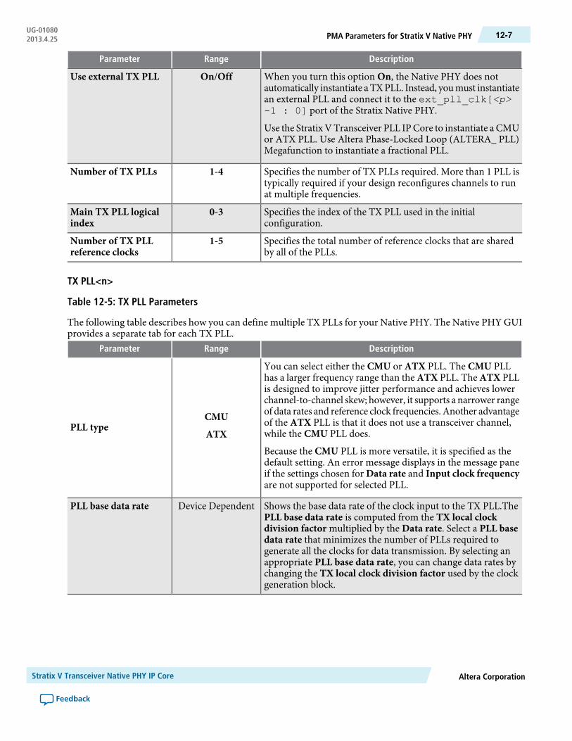
DescriptionRangeParameter
When you turn this option On, the Native PHY does notautomatically instantiate aTXPLL. Instead, youmust instantiatean external PLL and connect it to the ext_pll_clk[<p>-1 : 0] port of the Stratix Native PHY.
Use the Stratix VTransceiver PLL IPCore to instantiate a CMUor ATX PLL. Use Altera Phase-Locked Loop (ALTERA_ PLL)Megafunction to instantiate a fractional PLL.
On/OffUse external TX PLL
Specifies the number of TX PLLs required. More than 1 PLL istypically required if your design reconfigures channels to runat multiple frequencies.
1-4Number of TX PLLs
Specifies the index of the TX PLL used in the initialconfiguration.
0-3Main TX PLL logicalindex
Specifies the total number of reference clocks that are sharedby all of the PLLs.
1-5Number of TX PLLreference clocks
TX PLL<n>
Table 12-5: TX PLL Parameters
The following table describes how you can define multiple TX PLLs for your Native PHY. The Native PHY GUIprovides a separate tab for each TX PLL.
DescriptionRangeParameter
You can select either the CMU or ATX PLL. The CMU PLLhas a larger frequency range than the ATX PLL. The ATX PLLis designed to improve jitter performance and achieves lowerchannel-to-channel skew; however, it supports a narrower rangeof data rates and reference clock frequencies. Another advantageof the ATX PLL is that it does not use a transceiver channel,while the CMU PLL does.
Because the CMU PLL is more versatile, it is specified as thedefault setting. An error message displays in the message paneif the settings chosen for Data rate and Input clock frequencyare not supported for selected PLL.
CMU
ATXPLL type
Shows the base data rate of the clock input to the TX PLL.ThePLL base data rate is computed from the TX local clockdivision factor multiplied by the Data rate. Select a PLL basedata rate that minimizes the number of PLLs required togenerate all the clocks for data transmission. By selecting anappropriate PLL base data rate, you can change data rates bychanging the TX local clock division factor used by the clockgeneration block.
Device DependentPLL base data rate
Altera CorporationStratix V Transceiver Native PHY IP Core
Feedback
12-7PMA Parameters for Stratix V Native PHYUG-010802013.4.25

DescriptionRangeParameter
Specifies the frequency of the reference clock for the Selectedreference clock source index you specify. You can define asingle frequency for each PLL. You can use the TransceiverReconfiguration Controller shown in Stratix V NativeTransceiver PHY IP Core to dynamically change the referenceclock input to the PLL.
Note that the list of frequencies updates dynamically when youchange the Data rate.
The Input clock frequency drop down menu is populated withall valid frequencies derived as a function of the data rate andbase data rate. However, if fb_compensation is selected as thebonding mode then the input reference clock frequency islimited to the data rate divided by the PCS-PMA interfacewidth.
Device DependentReference clockfrequency
You can define up to 5 frequencies for the PLLs in your core.TheReference clock frequency selected for index 0 , is assignedto TX PLL<0>. The Reference clock frequency selected forindex 1 , is assigned to TX PLL<1>, and so on.
0-4Selected reference clocksource
RX CDR Options
Table 12-6: RX PMA Parameters
The following table describes the RXCDRoptions you can specify. Formore information about theCDR circuitry,refer to the Receiver Clock Data Recovery Unit section in Clock Networks and PLLs in Stratix V Devices.
DescriptionRangeParameter
When you turn this option On, you can dynamically changethe reference clock input the CDR circuit. This option is alsorequired to simulate TX PLL reconfiguration.
On/OffEnable CDR dynamicreconfiguration
Specifies the number of reference clocks for the CDRs.1-5Number of CDRreference clocks
Specifies the index of the selected CDR reference clock.0-4SelectedCDRreferenceclock
Specifies the frequency of the clock input to the CDR.Device DependentSelectedCDRreferenceclock frequency
Specifies the maximum PPM difference the CDR can toleratebetween the input reference clock and the recovered clock.
Device DependentPPMdetector threshold
When you turn this option On, the rx_is_lockedtodataport is an output of the PMA.On/OffEnable
rx_is_lockedtodataport
When you turn this option On, the rx_is_lockedtorefport is an output of the PMA.
On/OffEnablerx_is_lockedtoref port
When you turn this option On, the rx_set_locktodataand rx_set_locktoref ports are outputs of the PMA.
On/OffEnablerx_set_locktodata andrx_set_locktoref ports
Stratix V Transceiver Native PHY IP CoreAltera Corporation
Feedback
UG-01080PMA Parameters for Stratix V Native PHY12-8 2013.4.25
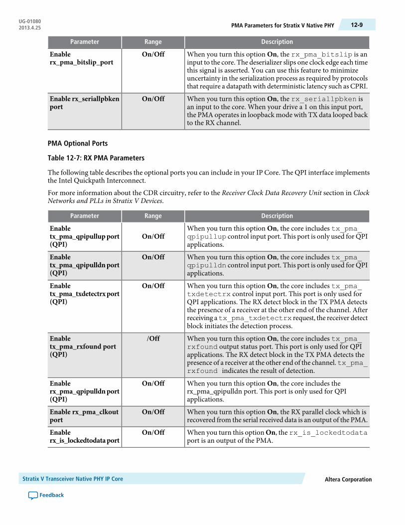
DescriptionRangeParameter
When you turn this option On, the rx_pma_bitslip is aninput to the core. The deserializer slips one clock edge each timethis signal is asserted. You can use this feature to minimizeuncertainty in the serialization process as required by protocolsthat require a datapathwith deterministic latency such as CPRI.
On/OffEnablerx_pma_bitslip_port
When you turn this option On, the rx_seriallpbken isan input to the core. When your drive a 1 on this input port,the PMA operates in loopback mode with TX data looped backto the RX channel.
On/OffEnable rx_seriallpbkenport
PMA Optional Ports
Table 12-7: RX PMA Parameters
The following table describes the optional ports you can include in your IP Core. The QPI interface implementsthe Intel Quickpath Interconnect.
For more information about the CDR circuitry, refer to the Receiver Clock Data Recovery Unit section in ClockNetworks and PLLs in Stratix V Devices.
DescriptionRangeParameter
When you turn this option On, the core includes tx_pma_qpipullup control input port. This port is only used for QPIapplications.
On/OffEnabletx_pma_qpipullupport(QPI)
When you turn this option On, the core includes tx_pma_qpipulldn control input port. This port is only used for QPIapplications.
On/OffEnabletx_pma_qpipulldnport(QPI)
When you turn this option On, the core includes tx_pma_txdetectrx control input port. This port is only used forQPI applications. The RX detect block in the TX PMA detectsthe presence of a receiver at the other end of the channel. Afterreceiving atx_pma_txdetectrx request, the receiver detectblock initiates the detection process.
On/OffEnabletx_pma_txdetectrxport(QPI)
When you turn this option On, the core includes tx_pma_rxfound output status port. This port is only used for QPIapplications. The RX detect block in the TX PMA detects thepresence of a receiver at the other end of the channel.tx_pma_rxfound indicates the result of detection.
/OffEnabletx_pma_rxfound port(QPI)
When you turn this option On, the core includes therx_pma_qpipulldn port. This port is only used for QPIapplications.
On/OffEnablerx_pma_qpipulldnport(QPI)
When you turn this option On, the RX parallel clock which isrecovered from the serial received data is an output of the PMA.
On/OffEnable rx_pma_clkoutport
When you turn this option On, the rx_is_lockedtodataport is an output of the PMA.
On/OffEnablerx_is_lockedtodataport
Altera CorporationStratix V Transceiver Native PHY IP Core
Feedback
12-9PMA Parameters for Stratix V Native PHYUG-010802013.4.25

DescriptionRangeParameter
When you turn this option On, the rx_is_lockedtorefport is an output of the PMA.
On/OffEnablerx_is_lockedtoref port
When you turn this option On, the rx_set_lockedtdataand rx_set_lockedtoref ports are outputs of the PMA.
On/OffEnablerx_set_lockedtodataand rx_set_locktorefports
When you turn this option On, the rx_pma_bitslip is aninput to the core. The deserializer slips one clock edge each timethis signal is asserted. You can use this feature to minimizeuncertainty in the serialization process as required by protocolsthat require a datapathwith deterministic latency such as CPRI.
On/OffEnablerx_pma_bitslip_port
When you turn this option On, the rx_seriallpbken isan input to the core. When your drive a 1 on this input port,the PMA operates in loopback mode with TX data looped backto the RX channel.
On/OffEnable rx_seriallpbkenport
The following table lists the best case latency for the most significant bit of a word for the RX deserializerfor the PMA Direct datapath. For example, for an 8-bit interface width, the latencies in UI are 11 for bit 7,12 for bit 6, 13 for bit 5, and so on.
Table 12-8: Latency for RX Deserialization in Stratix V Devices
Stratix V Latency in UIFPGA Fabric Interface Width
118 bits
1310 bits
1916 bits
2320 bits
3532 bits
4340 bits
9964 bits
12380 bits
Table 12-9: Latency for TX Serialization in Stratix V Devices
The following table lists the best- case latency for the LSB of the TX serializer for all supported interface widthsfor the PMA Direct datapath.
Stratix V Latency in UIFPGA Fabric Interface Width
448 bits
5410 bits
6816 bits
8420 bits
10032 bits
Stratix V Transceiver Native PHY IP CoreAltera Corporation
Feedback
UG-01080PMA Parameters for Stratix V Native PHY12-10 2013.4.25

Stratix V Latency in UIFPGA Fabric Interface Width
12440 bits
13264 bits
16480 bits
The following tables lists the bits used for all FPGA fabric to PMA interface widths. Regardless of the FPGAFabric Interface Width selected, all 80 bits are exposed for the TX and RX parallel data ports. However,depending upon the interface width selected not all bits on the bus will be active. The following table listswhich bits are active for each FPGA Fabric Interface Width selection. For example, if your interface is 16bits, the active bits on the bus are [17:0] and [7:0] of the 80 bit bus. The non-active bits are tied to ground.
Table 12-10: Active Bits for Each Fabric Interface Width in PMA Direct Mode
Bus Bits UsedFPGA Fabric Interface Width
[7:0]8 bits
[9:0]10 bits
{[17:10], [7:0]}16 bits
[19:0]20 bits
{[37:30], [27:20], [17:10], [7:0]}32 bits
[39:0]40 bits
{[77:70], [67:60], [57:50], [47:40], [37:30], [27:20],[17:10], [7:0]}
64 bits
[79:0]80 bits
Related InformationTransceiver Architecture in Stratix V Devices
Stratix V Device Datasheet
Clock Networks and PLLs in Stratix V Devices
Standard PCS Parameters for Stratix V Native PHYThis section shows the complete datapath and clocking for the Standard PCS and defines the parametersavailable in the GUI to enable or disable the individual blocks in the Standard PCS.
Altera CorporationStratix V Transceiver Native PHY IP Core
Feedback
12-11Standard PCS Parameters for Stratix V Native PHYUG-010802013.4.25
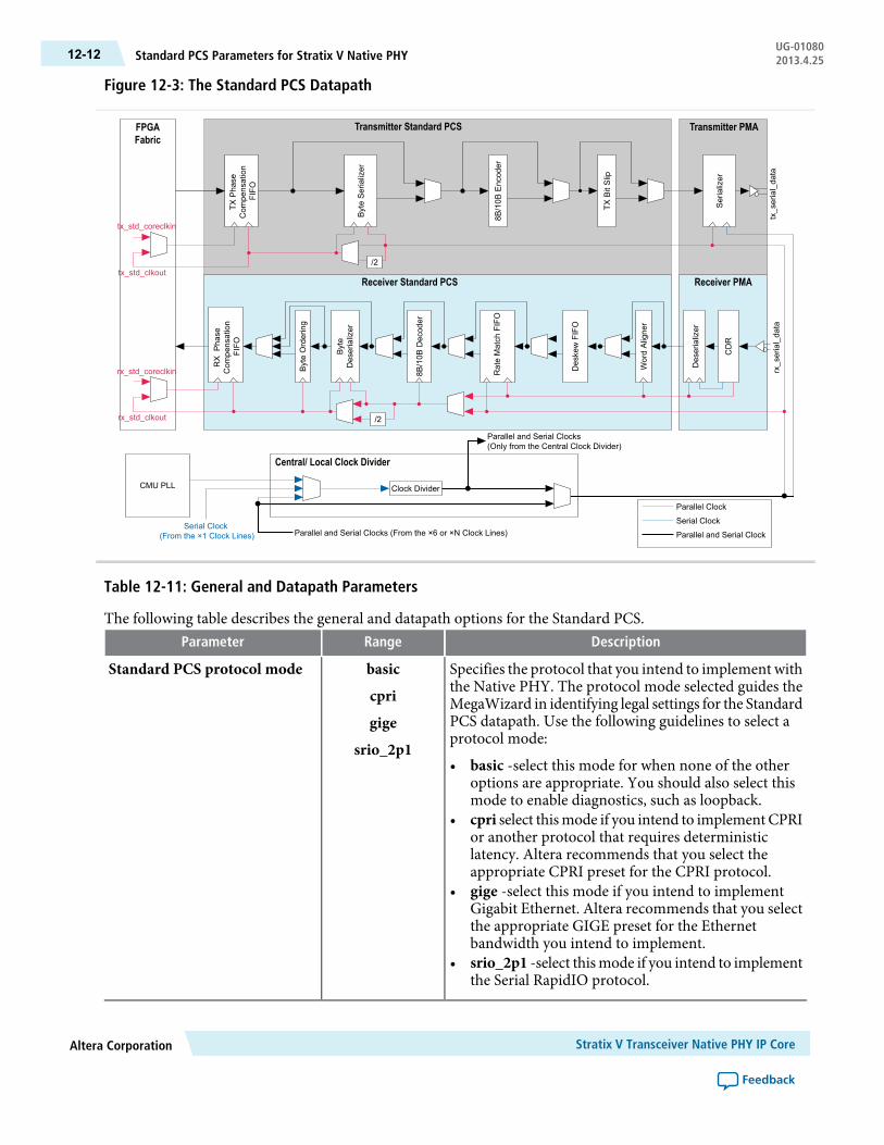
Figure 12-3: The Standard PCS Datapath
RX
Pha
seCom
pensation
FIFO
ByteOrdering
Byte
Deserializer
8B/10B
Decod
er
RateMatch
FIFO
Receiver Standard PCS Receiver PMA
DeskewFIFO
WordAligne
r
Deserializer
CDR
Transmitter Standard PCS Transmitter PMA
Serializer
tx_serial_da
tarx_serial_da
ta
FPGAFabric
TXPha
seCom
pensation
FIFO
ByteSerializer
8B/10B
Encod
er
TXBitSlip
/2
/2
Parallel Clock
Serial Clock
Parallel and Serial Clock
Clock Divider
Parallel and Serial Clocks (From the ×6 or ×N Clock Lines)Serial Clock
(From the ×1 Clock Lines)
Central/ Local Clock Divider
Parallel and Serial Clocks(Only from the Central Clock Divider)
CMU PLL
tx_std_coreclkin
rx_std_coreclkin
rx_std_clkout
tx_std_clkout
Table 12-11: General and Datapath Parameters
The following table describes the general and datapath options for the Standard PCS.DescriptionRangeParameter
Specifies the protocol that you intend to implement withthe Native PHY. The protocol mode selected guides theMegaWizard in identifying legal settings for the StandardPCS datapath. Use the following guidelines to select aprotocol mode:
• basic -select this mode for when none of the otheroptions are appropriate. You should also select thismode to enable diagnostics, such as loopback.
• cpri select thismode if you intend to implementCPRIor another protocol that requires deterministiclatency. Altera recommends that you select theappropriate CPRI preset for the CPRI protocol.
• gige -select this mode if you intend to implementGigabit Ethernet. Altera recommends that you selectthe appropriate GIGE preset for the Ethernetbandwidth you intend to implement.
• srio_2p1 -select thismode if you intend to implementthe Serial RapidIO protocol.
basic
cpri
gige
srio_2p1
Standard PCS protocol mode
Stratix V Transceiver Native PHY IP CoreAltera Corporation
Feedback
UG-01080Standard PCS Parameters for Stratix V Native PHY12-12 2013.4.25
DescriptionRangeParameter
Specifies the width of the datapath that connects theFPGA fabric to the PMA. The transceiver interface widthdepends upon whether you enable 8B/10B. To simplifyconnectivity between the FPGA fabric and PMA, the busbits used are not contiguous for 16- and 32-bit buses.16-, 32-, and 64-bit buses. Refer to Table 12-10 for thebits used.
8, 10, 16,
20, 32, 40
64, 80
Standard PCS/PMA interfacewidth
Shows the FPGA fabric to TXPCS interface widthwhichis calculated from the Standard PCS/PMA interfacewidth.
8, 10, 16, 20FPGA fabric/Standard TX PCSinterface width
Shows the FPGA fabric to RXPCS interface widthwhichis calculated from the Standard PCS/PMA interfacewidth.
8, 10, 16, 20FPGA fabric/Standard RX PCSinterface width
When you turn this option On, all PCS functions aredisabled. This option creates a the lowest latency NativePHY that allows dynamic reconfigure between multiplePCS datapaths.
On/ OffEnable Standard PCS lowlatency mode
Phase Compensation FIFO
The phase compensation FIFO assures clean data transfer to and from the FPGA fabric by compensatingfor the clock phase difference between the low-speed parallel clock and FPGA fabric interface clock. Thefollowing table describes the options for the phase compensation FIFO.
Table 12-12: Phase Compensation FIFO Parameters
DescriptionRangeParameter
The following 2 modes are possible:
• low_latency : This mode adds 3-4 cycles of latency tothe TX datapath.
• register_fifo : In this mode the FIFO is replaced byregisters to reduce the latency through the PCS. Usethis mode for protocols that require deterministiclatency, such as CPRI.
low_latency
register_fifo
TX FIFO mode
The following 2 modes are possible:
• low_latency : This mode adds 2-3 cycles of latency tothe TX datapath.
• register_fifo : In this mode the FIFO is replaced byregisters to reduce the latency through the PCS. Usethis mode for protocols that require deterministiclatency, such as CPRI.
low_latency
register_fifo
RX FIFO mode
When you turn this option On, the TX Phasecompensation FIFO outputs a FIFO full status flag.
On/OffEnable tx_std_pcfifo_full port
When you turn this option On, the TX Phasecompensation FIFO outputs a FIFO empty status flag.
On/OffEnable tx_std_pcfifo_emptyport
Altera CorporationStratix V Transceiver Native PHY IP Core
Feedback
12-13Standard PCS Parameters for Stratix V Native PHYUG-010802013.4.25
DescriptionRangeParameter
When you turn this option On, the RX Phasecompensation FIFO outputs a FIFO full status flag.
On/OffEnable rx_std_pcfifo_full port
When you turn this option On, the RX Phasecompensation FIFO outputs a FIFO empty status flag.
On/ OffEnable rx_std_pcfifo_emptyport
Byte Ordering Block Parameters
TheRXbyte ordering block realigns the data coming from the byte deserializer. This block is necessarywhenthe PCS to FPGA fabric interface width is greater than the PCS datapath. Because the timing of the RX PCSreset logic is indeterminate, the byte ordering at the output of the byte deserializer may or may not matchthe original byte ordering of the transmitted data. The following table describes the byte ordering blockparameters.
DescriptionRangeParameter
When you turn this optionOn, the PCS includes the byteordering block.
On/OffEnable RX byte ordering
Specifies the control mode for the byte ordering block.The following modes are available:
• Manual : Allows you to control the byte orderingblock
• Auto : The word aligner automatically controls thebyte ordering block once word alignment is achieved.
manual
auto
Byte ordering control mode
Showswidth of the pad that youmust specify. This widthdepends upon the PCS width and whether nor not8B/10B encoding is used as follows:
Width 8B/10B Pad Pattern8/16,32 No 8 bits10,20,40 No 10 bits8,16,32 Yes 9 bits
8-10Byte ordering pattern width
Specifies the number of symbols theword aligner shouldsearch for. When the PMA is 16 or 20 bits wide, the byteordering block can optionally search for 1 or 2 symbols.
1-2Byte ordering symbol count
Specifies the search pattern for the byte ordering block.User-specified8-10 bit pattern
Byte order pattern (hex)
Stratix V Transceiver Native PHY IP CoreAltera Corporation
Feedback
UG-01080Standard PCS Parameters for Stratix V Native PHY12-14 2013.4.25

DescriptionRangeParameter
Specifies the pad pattern that is inserted by the byteordering block. This value is insertedwhen the byte orderpattern is recognized.
The byte ordering pattern should occupy the leastsignificant byte (LSB) of the parallel TX data. If the byteordering block identifies the programmed byte orderingpattern in the most significant byte (MSB) of thebyte-deserialized data, it inserts the appropriate numberof user-specified pad bytes to push the byte orderingpattern to the LSB position, restoring proper byteordering.
User-specified8-10 bit pattern
Byte order pad value (hex)
Enables the optional rx_std_byte_order_enacontrol input port. When this signal is asserted, the byteordering block initiates a byte ordering operation if theByte ordering controlmode is set tomanual. Once byteordering has occurred, you must deassert and reassertthis signal to perform another byte ordering operation.This signal is an synchronous input signal; however, itmust be asserted for at least 1 cycle ofrx_std_clkout.
On/OffEnable rx_std_byteorder_enaport
Enables the optional rx_std_byteorder_flagstatus output port.When asserted, indicates that the byteordering block has performed a byte order operation.This signal is asserted on the clock cycle in which byteordering occurred. This signal is synchronous to therx_std_clkout clock.
On/OffEnable rx_std_byteorder_flagport
Byte Serializer and Deserializer
The byte serializer and deserializer allow the PCS to operate at twice the data width of the PMA serializer.This feature allows the PCS to run at a lower frequency and accommodate a wider range of FPGA interfacewidths. The following table describes the byte serialization and deserialization options you can specify.
Table 12-13: Byte Serializer and Deserializer Parameters
DescriptionRangeParameter
When you turn this option On, the PCS includes a TXbyte serializer which allows the PCS to run at a lowerclock frequency to accommodate a wider range of FPGAinterface widths.
On/OffEnable TX byte serializer
When you turn this option On, the PCS includes an RXbyte deserializer and deserializer which allows the PCSto run at a lower clock frequency to accommodate awiderrange of FPGA interface widths.
On/OffEnable RX byte deserializer
8B/10B
The 8B/10B encoder generates 10-bit code groups from the 8-bit data and 1-bit control identifier. In 8-bitwidth mode, the 8B/10B encoder translates the 8-bit data to a 10-bit code group (control word or data word)
Altera CorporationStratix V Transceiver Native PHY IP Core
Feedback
12-15Standard PCS Parameters for Stratix V Native PHYUG-010802013.4.25
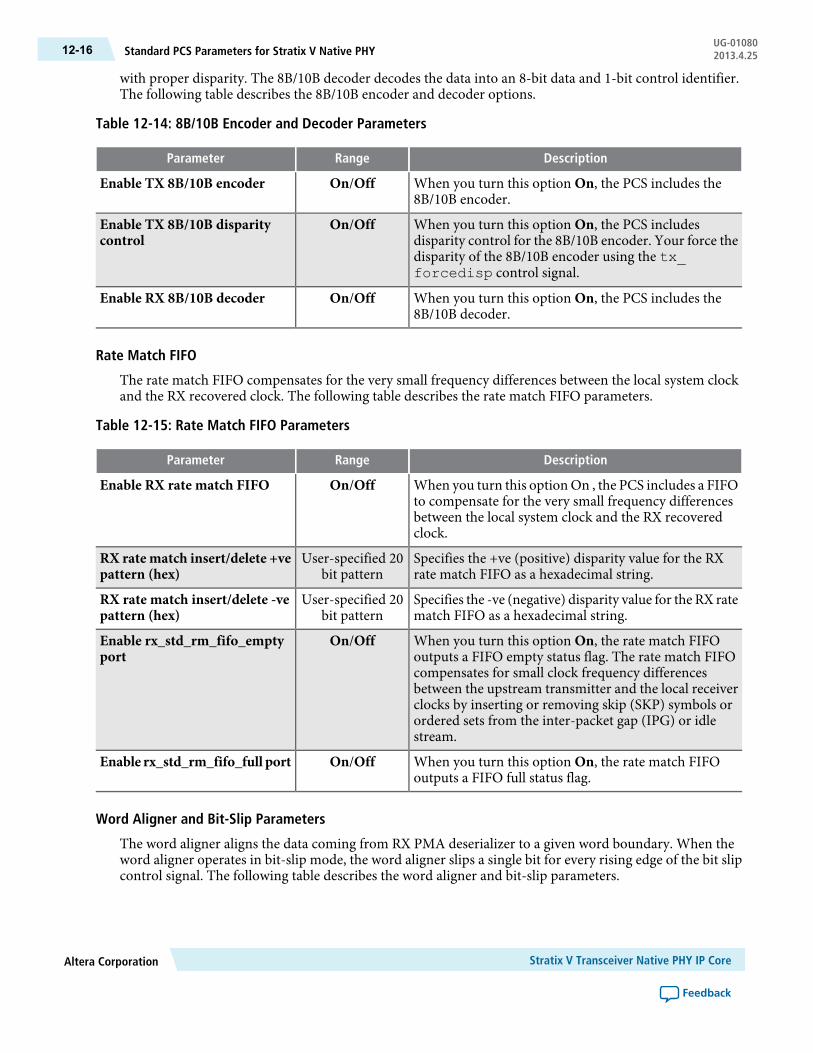
with proper disparity. The 8B/10B decoder decodes the data into an 8-bit data and 1-bit control identifier.The following table describes the 8B/10B encoder and decoder options.
Table 12-14: 8B/10B Encoder and Decoder Parameters
DescriptionRangeParameter
When you turn this option On, the PCS includes the8B/10B encoder.
On/OffEnable TX 8B/10B encoder
When you turn this option On, the PCS includesdisparity control for the 8B/10B encoder. Your force thedisparity of the 8B/10B encoder using the tx_forcedisp control signal.
On/OffEnable TX 8B/10B disparitycontrol
When you turn this option On, the PCS includes the8B/10B decoder.
On/OffEnable RX 8B/10B decoder
Rate Match FIFO
The rate match FIFO compensates for the very small frequency differences between the local system clockand the RX recovered clock. The following table describes the rate match FIFO parameters.
Table 12-15: Rate Match FIFO Parameters
DescriptionRangeParameter
When you turn this option On , the PCS includes a FIFOto compensate for the very small frequency differencesbetween the local system clock and the RX recoveredclock.
On/OffEnable RX rate match FIFO
Specifies the +ve (positive) disparity value for the RXrate match FIFO as a hexadecimal string.
User-specified 20bit pattern
RX ratematch insert/delete +vepattern (hex)
Specifies the -ve (negative) disparity value for the RX ratematch FIFO as a hexadecimal string.
User-specified 20bit pattern
RX rate match insert/delete -vepattern (hex)
When you turn this option On, the rate match FIFOoutputs a FIFO empty status flag. The rate match FIFOcompensates for small clock frequency differencesbetween the upstream transmitter and the local receiverclocks by inserting or removing skip (SKP) symbols orordered sets from the inter-packet gap (IPG) or idlestream.
On/OffEnable rx_std_rm_fifo_emptyport
When you turn this option On, the rate match FIFOoutputs a FIFO full status flag.
On/OffEnable rx_std_rm_fifo_full port
Word Aligner and Bit-Slip Parameters
The word aligner aligns the data coming from RX PMA deserializer to a given word boundary. When theword aligner operates in bit-slip mode, the word aligner slips a single bit for every rising edge of the bit slipcontrol signal. The following table describes the word aligner and bit-slip parameters.
Stratix V Transceiver Native PHY IP CoreAltera Corporation
Feedback
UG-01080Standard PCS Parameters for Stratix V Native PHY12-16 2013.4.25
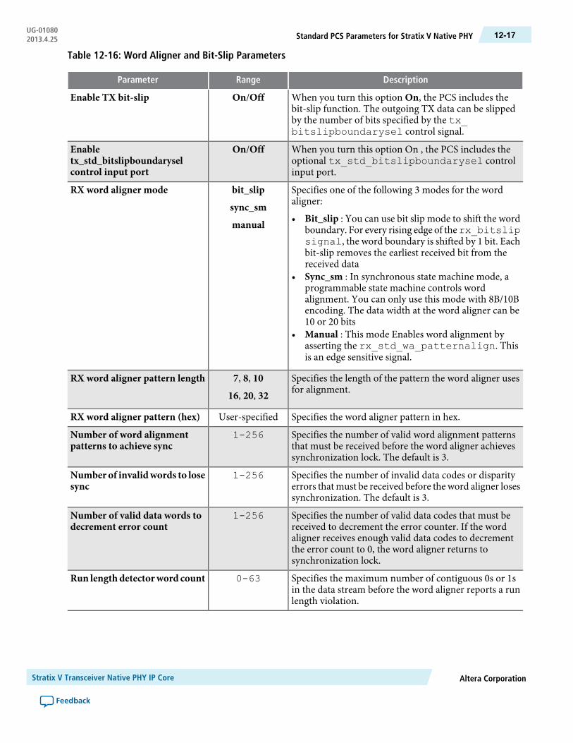
Table 12-16: Word Aligner and Bit-Slip Parameters
DescriptionRangeParameter
When you turn this option On, the PCS includes thebit-slip function. The outgoing TX data can be slippedby the number of bits specified by the tx_bitslipboundarysel control signal.
On/OffEnable TX bit-slip
When you turn this option On , the PCS includes theoptional tx_std_bitslipboundarysel controlinput port.
On/OffEnabletx_std_bitslipboundaryselcontrol input port
Specifies one of the following 3 modes for the wordaligner:
• Bit_slip : You can use bit slip mode to shift the wordboundary. For every rising edge of therx_bitslipsignal, the word boundary is shifted by 1 bit. Eachbit-slip removes the earliest received bit from thereceived data
• Sync_sm : In synchronous state machine mode, aprogrammable state machine controls wordalignment. You can only use this mode with 8B/10Bencoding. The data width at the word aligner can be10 or 20 bits
• Manual : This mode Enables word alignment byasserting the rx_std_wa_patternalign. Thisis an edge sensitive signal.
bit_slip
sync_sm
manual
RX word aligner mode
Specifies the length of the pattern the word aligner usesfor alignment.
7, 8, 10
16, 20, 32
RX word aligner pattern length
Specifies the word aligner pattern in hex.User-specifiedRX word aligner pattern (hex)
Specifies the number of valid word alignment patternsthat must be received before the word aligner achievessynchronization lock. The default is 3.
1-256Number of word alignmentpatterns to achieve sync
Specifies the number of invalid data codes or disparityerrors thatmust be received before the word aligner losessynchronization. The default is 3.
1-256Number of invalidwords to losesync
Specifies the number of valid data codes that must bereceived to decrement the error counter. If the wordaligner receives enough valid data codes to decrementthe error count to 0, the word aligner returns tosynchronization lock.
1-256Number of valid data words todecrement error count
Specifies the maximum number of contiguous 0s or 1sin the data stream before the word aligner reports a runlength violation.
0-63Run lengthdetectorword count
Altera CorporationStratix V Transceiver Native PHY IP Core
Feedback
12-17Standard PCS Parameters for Stratix V Native PHYUG-010802013.4.25

DescriptionRangeParameter
Enables the optional rx_std_wa_patternaligncontrol input port. A rising edge on this signal causesthe word aligner to align the next incoming wordalignment pattern when the word aligner is configuredin manual mode.
On/OffEnable rx_std_wa_patternalignport
Enables the optional rx_std_wa_a1a2size controlinput port.
On/OffEnable rx_std_wa_a1a2size port
Enables the optional rx_std_wa_bitslipboundarysel status output port.
On/OffEnablerx_std_wa_bitslipboundaryselport
Enables the optional rx_std_wa_bitslip controlinput port.
On/OffEnable rx_std_wa_bitslip port
Enables the optional rx_std_wa_runlength_errcontrol input port.
On/OffEnablerx_std_wa_runlength_err port
Bit Reversal and Polarity Inversion
These functions allow you to reverse bit order, byte order, and polarity to correct errors and to accommodatedifferent layouts of data. The following table describes these parameters.
DescriptionRangeParameter
When you turn this optionOn, the word aligner reversesTX parallel data before transmitting it to the PMA forserialization. You can only change this static setting usingthe Transceiver Reconfiguration Controller.
On/OffEnable TX bit reversal
When you turn this option On, the rx_st_bitrev_ena port controls bit reversal of the RX parallel dataafter it passes from the PMA to the PCS.
On/OffEnable RX bit reversal
When you turn this optionOn, the word aligner reversesthe byte order before transmitting data. This functionallows you to reverse the order of bytes that wereerroneously swapped. The PCS can swap the ordering ofboth 8 and10 bit words.
On/OffEnable RX byte reversal
When you turn this option On, the tx_std_polinvport controls polarity inversion of TXparallel data beforetransmitting the parallel data to the PMA.
On/OffEnable TX polarity inversion
When you turn this option On, asserting rx_std_polinv controls polarity inversion of RX parallel dataafter PMA transmission.
On/OffEnable RX polarity inversion
When you turn this option On, asserting rx_std_bitrev_ena control port causes the RX data order tobe reversed from the normal order, LSB to MSB, to theopposite, MSB to LSB. This signal is an asynchronousinput.
On/OffEnable rx_std_bitrev_ena port
Stratix V Transceiver Native PHY IP CoreAltera Corporation
Feedback
UG-01080Standard PCS Parameters for Stratix V Native PHY12-18 2013.4.25
DescriptionRangeParameter
When you turn this option On, asserting rx_std_byterev_ena input control port causes swaps theorder of the individual 8- or 10-bit words received fromthe PMA.
On/OffEnable rx_std_byterev_enaport
When you turn this option On, the tx_std_polinvinput is enabled. You can use this control port to swapthe positive and negative signals of a serial differentiallink if they were erroneously swapped during boardlayout.
On/OffEnable tx_std_polinv port
When you turn this option On, the rx_std_polinvinput is enabled. You can use this control port to swapthe positive and negative signals of a serial differentiallink if they were erroneously swapped during boardlayout.
On/OffEnable rx_std_polinv port
Whenyou turn this optionOn, thetx_std_elecidleinput port is enabled. When this signal is asserted, itforces the transmitter to electrical idle. This signal isrequired for the PCI Express protocol.
On/OffEnable tx_std_elecidle port
When you turn this option On, the optional tx_std_signaldetect output port is enabled. This signal isrequired for the PCI Express protocol. If enabled, thesignal threshold detection circuitry senses whether thesignal level present at the RX input buffer is above thesignal detect threshold voltage that you specified.
On/OffEnable rx_std_signaldetect port
Related InformationTransceiver Architecture in Stratix V Devices
10G PCS Parameters for Stratix V Native PHYThis section shows the complete datapath and clocking for the 10G PCS and defines parameters availablein the GUI to enable or disable the individual blocks in the 10G PCS.
Altera CorporationStratix V Transceiver Native PHY IP Core
Feedback
12-1910G PCS Parameters for Stratix V Native PHYUG-010802013.4.25
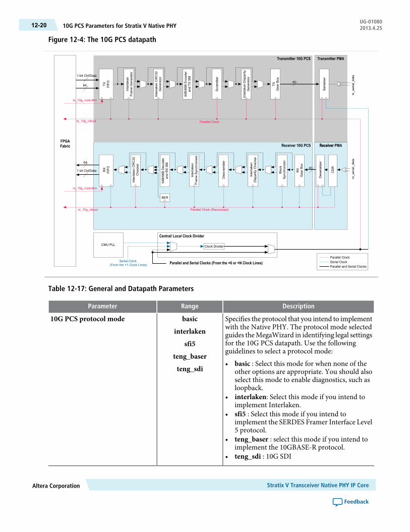
Figure 12-4: The 10G PCS datapath
FPGAFabric
Transmitter 10G PCS
Receiver 10G PCS
Transmitter PMA
Receiver PMA
TX FIFO
RX
FIFO
Interla
ken
Fram
eGen
erator
Interla
kenCRC32
Gen
erator
Interla
kenCRC32
Che
cker
64B/66B
Encod
eran
dTX
SM
64B/66B
Decod
eran
dRXSM
Scram
bler
Descram
bler
Interla
ken
Dispa
rityChe
cker
Block
Synchronizer
Interla
ken
Fram
eSynchronizer
Interla
kenDispa
rity
Gen
erator
TXGea
rBox
RX
Gea
rBox
64
64
Parallel Clock (Recovered)
Parallel Clock
40
Serializer
Deserializer
CDR
tx_serial_da
tarx_serial_da
ta
1-bit Ctrl/Data
1 bit Ctrl/Data40
Clock Divider
BER
Parallel and Serial Clocks (From the ×6 or ×N Clock Lines)Serial Clock(From the ×1 Clock Lines)
Central/ Local Clock Divider
Parallel ClockSerial ClockParallel and Serial Clocks
CMU PLL
tx_10g_coreclkin
rx_10g_coreclkin
tx_10g_clkout
rx_10g_clkout
Table 12-17: General and Datapath Parameters
DescriptionRangeParameter
Specifies the protocol that you intend to implementwith the Native PHY. The protocol mode selectedguides theMegaWizard in identifying legal settingsfor the 10G PCS datapath. Use the followingguidelines to select a protocol mode:
• basic : Select this mode for when none of theother options are appropriate. You should alsoselect this mode to enable diagnostics, such asloopback.
• interlaken: Select this mode if you intend toimplement Interlaken.
• sfi5 : Select this mode if you intend toimplement the SERDES Framer Interface Level5 protocol.
• teng_baser : select this mode if you intend toimplement the 10GBASE-R protocol.
• teng_sdi : 10G SDI
basic
interlaken
sfi5
teng_baser
teng_sdi
10G PCS protocol mode
Stratix V Transceiver Native PHY IP CoreAltera Corporation
Feedback
UG-0108010G PCS Parameters for Stratix V Native PHY12-20 2013.4.25

DescriptionRangeParameter
Specifies the width of the datapath that connectsthe FPGA fabric to the PMA.
32, 40, 6410G PCS/PMA interface width
Specifies the FPGA fabric to TX PCS interfacewidth .
The 66-bit FPGA fabric/PCS interface width isachieved using 64-bits from the TX andRXparalleldata and the lower 2-bits from the control bus.
The 67-bit FPGA fabric/PCS interface width isachieved using the 64-bits from the TX and RXparallel data and the lower 3-bits from the controlbus.
32, 40, 50
64, 66, 67
FPGA fabric/10G PCS interfacewidth
10G TX FIFO
The TX FIFO is the interface between TX data from the FPGA fabric and the PCS. This FIFO is anasynchronous 73-bit wide, 32-deep memory buffer It also provides full, empty, partially full, and empty flagsbased on programmable thresholds. The following table describes the 10G TX FIFO parameters.
Table 12-18: 10G TX FIFO Parameters
DescriptionRangeParameter
Specifies one of the following 3 modes:
• interlaken : The TX FIFO acts as an elasticbuffer. The FIFO write clock frequency(coreclk) can exceed that of the effective readclock, tx_clkout. You can control writes tothe FIFO with tx_data_valid. Bymonitoring the FIFO flags, you can avoid theFIFO full and empty conditions. The Interlakenframe generator controls reads.
• phase_comp : The TX FIFO compensates forthe clock phase difference between thecoreclkin and tx_clkout which is aninternal PCS clock.
• register : The TX FIFO is bypassed. tx_dataand tx_data_valid are registered at theFIFO output. You must control tx_data_validprecisely based on gearbox ratio to avoidgearbox underflow or overflow conditions.
Interlaken
phase_comp
register
TX FIFO Mode
Specifies the full threshold for the 10G PCS TXFIFO. The active high TX FIFO full flag issynchronous tocoreclk. The default value is 31.
0-31TX FIFO full threshold
Specifies the empty threshold for the 10G PCS TXFIFO. The active high TX FIFO empty flag issynchronous to coreclk. The default value is 0.
0-31TX FIFO empty threshold
Altera CorporationStratix V Transceiver Native PHY IP Core
Feedback
12-2110G PCS Parameters for Stratix V Native PHYUG-010802013.4.25
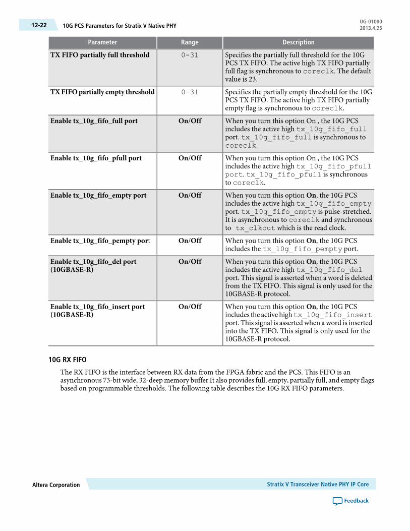
DescriptionRangeParameter
Specifies the partially full threshold for the 10GPCS TX FIFO. The active high TX FIFO partiallyfull flag is synchronous to coreclk. The defaultvalue is 23.
0-31TX FIFO partially full threshold
Specifies the partially empty threshold for the 10GPCS TX FIFO. The active high TX FIFO partiallyempty flag is synchronous to coreclk.
0-31TXFIFOpartially empty threshold
When you turn this option On , the 10G PCSincludes the active high tx_10g_fifo_fullport. tx_10g_fifo_full is synchronous tocoreclk.
On/OffEnable tx_10g_fifo_full port
When you turn this option On , the 10G PCSincludes the active high tx_10g_fifo_pfullport. tx_10g_fifo_pfull is synchronousto coreclk.
On/OffEnable tx_10g_fifo_pfull port
When you turn this option On, the 10G PCSincludes the active high tx_10g_fifo_emptyport. tx_10g_fifo_empty is pulse-stretched.It is asynchronous to coreclk and synchronousto tx_clkout which is the read clock.
On/OffEnable tx_10g_fifo_empty port
When you turn this option On, the 10G PCSincludes the tx_10g_fifo_pempty port.
On/OffEnable tx_10g_fifo_pempty port
When you turn this option On, the 10G PCSincludes the active high tx_10g_fifo_delport. This signal is asserted when a word is deletedfrom the TX FIFO. This signal is only used for the10GBASE-R protocol.
On/OffEnable tx_10g_fifo_del port(10GBASE-R)
When you turn this option On, the 10G PCSincludes the active hightx_10g_fifo_insertport. This signal is asserted when a word is insertedinto the TX FIFO. This signal is only used for the10GBASE-R protocol.
On/OffEnable tx_10g_fifo_insert port(10GBASE-R)
10G RX FIFO
The RX FIFO is the interface between RX data from the FPGA fabric and the PCS. This FIFO is anasynchronous 73-bit wide, 32-deep memory buffer It also provides full, empty, partially full, and empty flagsbased on programmable thresholds. The following table describes the 10G RX FIFO parameters.
Stratix V Transceiver Native PHY IP CoreAltera Corporation
Feedback
UG-0108010G PCS Parameters for Stratix V Native PHY12-22 2013.4.25

Table 12-19: 10G RX FIFO Parameters
DescriptionRangeParameter
Specifies one of the following 3 modes:
• interlaken : Select this mode for the Interlakenprotocol. To implement the deskew process. Inthis mode the FIFO acts as an elastic buffer. TheFIFO write clock can exceed the read clock.Your implementation must control the FIFOwrite (tx_datavalid) by monitoring theFIFO flags. The read enable is controlled by theInterlaken Frame Generator.
• clk_comp : This mode compensates for theclock difference between the PLD clock(coreclkin) and rxclkout. After blocklock is achieved, idle ordered set insertions anddeletions compensate for the clock differencebetween RX PMA clock and PLD clock up to ±100 ppm.
• phase_comp : This mode compensates for theclock phase difference between the PLD clock(coreclkin) andrxclkout. Use thismodefor 10GBASE-R.
• register : The TX FIFO is bypassed. rx_dataand rx_data_valid are registered at theFIFO output.
Interlaken
clk_comp
phase_comp
register
TX FIFO Mode
Specifies the full threshold for the 10G PCS RXFIFO. The default value is 31.
0-31RX FIFO full threshold
Specifies the empty threshold for the 10G PCS RXFIFO. The default value is 0.
0-31RX FIFO empty threshold
Specifies the partially full threshold for the 10GPCS RX FIFO. The default value is 23.
0-31RX FIFO partially full threshold
Specifies the partially empty threshold for the 10GPCS RX FIFO.
0-31RXFIFOpartially empty threshold
When you turn this optionOn, all alignmentwords(sync words), including the first sync word, areremoved after frame synchronization is achieved.If you enable this option, you must also enablecontrol word deletion.
On/OffEnable RX FIFO alignment worddeletion (Interlaken)
When you turn this option On , the rx_control_del parameter enables or disableswriting the Interlaken control word to RX FIFO.When disabled, a value of 0 for rx_control_del writes all control words to RX FIFO. Whenenabled, a value of 1 deletes all control words andonly writes the data to the RX FIFO.
On/OffEnable RX FIFO control worddeletion (Interlaken)
Altera CorporationStratix V Transceiver Native PHY IP Core
Feedback
12-2310G PCS Parameters for Stratix V Native PHYUG-010802013.4.25

DescriptionRangeParameter
When you turn this option On, the 10G PCSincludes the rx_data_valid signal whichIndicates when rx_data is valid. This option isavailable when you select the following parameters:
• 10G PCS protocol mode is Interlaken• 10G PCS protocol mode is Basic and RX FIFO
mode is phase_comp• 10G PCS protocol mode is Basic and RX FIFO
mode is register
On/OffEnable rx_10g_fifo_data_validport
When you turn this option On, the 10G PCSincludes the active high rx_10g_fifo_fullport. rx_10g_fifo_full is synchronous torx_clkout.
On/OffEnable rx_10g_fifo_full port
When you turn this option On, the 10G PCSincludes the active high rx_10g_fifo_pfullport. rx_10g_fifo_pfull is synchronous torx_clkout.
On/OffEnable rx_10g_fifo_pfull port
When you turn this option On, the 10G PCSincludes the active high rx_10g_fifo_emptyport.
On/OffEnable rx_10g_fifo_empty port
When you turn this option On, the 10G PCSincludes the rx_10g_fifo_pempty port.
On/OffEnable rx_10g_fifo_pempty port
When you turn this option On, the 10G PCSincludes therx_10g_fifo_delport. This signalis asserted when a word is deleted from the RXFIFO. This signal is only used for the 10GBASE-Rprotocol.
On/OffEnable rx_10g_fifo_del port(10GBASE-R)
When you turn this option On, the 10G PCSincludes the rx_10g_fifo_insert port. Thissignal is asserted when a word is inserted into theRX FIFO. This signal is only used for the10GBASE-R protocol.
On/OffEnable rx_10g_fifo_insert port(10GBASE-R)
When you turn this option On, the 10G PCSincludes the rx_10g_fifo_rd_en input port.Asserting this signal reads a word from the RXFIFO. This signal is only available for the Interlakenprotocol.
On/OffEnable rx_10g_fifo_rd_en port(Interlaken)
When you turn this option On, the 10G PCSincludes therx_10g_fifo_align_valoutputport. This signal is asserted when the wordalignment pattern is found. This signal is onlyavailable for the Interlaken protocol.
On/OffEnable rx_10g_fifo_align_val port(Interlaken)
Stratix V Transceiver Native PHY IP CoreAltera Corporation
Feedback
UG-0108010G PCS Parameters for Stratix V Native PHY12-24 2013.4.25

DescriptionRangeParameter
When you turn this option On, the 10G PCSincludes a divide by 33 clock output port. Youtypically need this option when the fabric to PCSinterface width is 66. Check location - moved toRX FIFO, but I don't know where
On/Offenable rx10g_clk33out port
When you turn this option On, the 10G PCSincludes the rx_10g_fifo_align_clr inputport. When this signal is asserted, the FIFO resetsand begins searching for a new alignment pattern.This signal is only available for the Interlakenprotocol.
On/OffEnable rx_10g_fifo_align_clr port(Interlaken)
When you turn this option On, the 10G PCSincludes the rx_10g_fifo_align_en inputport. This signal is used for FIFO deskew forInterlaken. When asserted, the correspondingchannel is enabled for alignment. This signal is onlyavailable for the Interlaken protocol.
On/OffEnable rx_10g_fifo_align_en port(Interlaken)
Interlaken Frame Generator
TX Frame generator generates the metaframe. It encapsulates the payload from MAC with the framing layercontrol words, including sync, scrambler, skip and diagnostic words. The following table describes theInterlaken frame generator parameters.
Table 12-20: Interlaken Frame Generator Parameters
DescriptionRangeParameter
When you turn this optionOn, the frame generatorblock of the 10G PCS is enabled.
On/Offteng_tx_framgen_enable
Specifies the metaframe length.0-8192teng_tx_framgen_user_length
When you turn this optionOn, the frame generatorburst functionality is enabled.
On/Offteng_tx_framgen_burst_enable
When you turn this option On, the 10G PCSincludes the tx_10g_frame output port. Whenasserted,tx_10g_frame indicates the beginningof a new metaframe inside the frame generator.
On/OffEnable tx_10g_frame port
When you turn this option On, the 10G PCSincludes the tx_10g_frame_diag_status2-bit input port. This port contains the lane StatusMessage from the framing layer Diagnostic Word,bits[33:32]. This message is inserted into the nextDiagnosticWord generated by the frame generationblock. The message must be held static for 5 cyclesbefore and 5 cycles after the tx_frame pulse.
On/OffEnable tx_10g_frame_diag_statusport
Altera CorporationStratix V Transceiver Native PHY IP Core
Feedback
12-2510G PCS Parameters for Stratix V Native PHYUG-010802013.4.25

DescriptionRangeParameter
When you turn this option On, the 10G PCSincludes the tx_10g_frame_burst_en inputport. This port controls frame generator data readsfrom the TX FIFO. The value of this signal islatched once at the beginning of each Metaframe.It controls whether data is read from the TX FIFOor SKIP Words are inserted for the currentMetaframe. Itmust be held static for 5 cycles beforeand 5 cycles after thetx_frame pulse.Whentx_10g_frame_burst_en is 0, the framegeneratordoes not read data from the TX FIFO for currentMetaframe. It insert SKIPs. When tx_10g_frame_burst_en is 1, the frame generator readsdata from the TX FIFO for current Metaframe.
On/OffEnable tx_10g_frame_burst_enport
Interlaken Frame Synchronizer
The Interlaken frame synchronizer block achieves lock by looking for four synchronization words inconsecutive metaframes. After synchronization, the frame synchronizer monitors the scrambler word in themetaframe and deasserts the lock signal after three consecutive mismatches and starts the synchronizationprocess again. Lock status is available to the FPGA fabric. The following table describes the Interlaken framesynchronizer parameters.
Table 12-21: Interlaken Frame Synchronizer Parameters
DescriptionRangeParameter
When you turn this optionOn, the 10GPCS framegenerator is enabled.
On/Offteng_tx_framsync_enable
When you turn this option On, the 10G PCSincludes the rx_10g_frame output port. Thissignal is asserted to indicate the beginning of a newmetaframe inside.
On/OffEnable rx_10g_frame port
When you turn this option On, the 10G PCSincludes therx_10g_frame_lock output port.This signal is asserted to indicate that the framesynchronization state machine has achieved framelock.
On/OffEnable rx_10g_frame_lock_port
When you turn this option On, the 10G PCSincludes therx_10g_frame_mfrm_erroutputport. This signal is asserted to indicate anmetaframe error.
On/OffEnable rx_10g_frame_mfrm_errport
When you turn this option On, the 10G PCSincludes therx_10g_frame_sync_erroutputport. This signal is asserted to indicatesynchronization control word errors. This signalremains asserted during the loss of block_lock anddoes not update until block_lock is recovered.
On/OffEnable rx_10g_frame_sync_errport
Stratix V Transceiver Native PHY IP CoreAltera Corporation
Feedback
UG-0108010G PCS Parameters for Stratix V Native PHY12-26 2013.4.25

DescriptionRangeParameter
When you turn this option On, the 10G PCSincludes therx_10g_frame_skip_insoutputport. This signal is asserted to indicate a SKIP wordwas received by the frame sync in a non-SKIPwordlocation within the metaframe.
On/OffEnable rx_10g_frame_skip_insport
When you turn this option On, the 10G PCSincludes therx_10g_frame_pyld_insoutputport. This signal is asserted to indicate a SKIP wordwas not received by the frame sync in a SKIP wordlocation within the metaframe.
On/OffEnable rx_10g_frame_pyld_insport
When you turn this option On, the 10G PCSincludes therx_10g_frame_skip_erroutputport. This signal is asserted to indicate the framesynchronization has received an erroneous wordin a Skip control word location within theMetaframe. This signal remains asserted during theloss of block_lock and does update until block_lockis recovered.
On/OffEnable rx_10g_frame_skip_errport
When you turn this option On, the 10G PCSincludes therx_10g_frame_diag_erroutputport. This signal is asserted to indicate a diagnosticcontrol word error. This signal remains assertedduring the loss of block_lock and does update untilblock_lock is recovered.
On/OffEnable rx_10g_frame_diag_errport
When you turn this option On, the 10G PCSincludes the rx_10g_frame_diag_status2-bit output port per channel. This port containsthe lane Status Message from the framing layerDiagnostic Word, bits[33:32]. This message isinserted into the next Diagnostic Word generatedby the frame generation block.
On/OffEnable rx_10g_frame_diag_statusport
Interlaken CRC32 Generator and Checker
CRC-32 provides a diagnostic tool on a per-lane basis. You can use CRC-32 to trace interface errors backto an individual lane. The CRC-32 calculation covers the whole metaframe including the Diagnostic Worditself. This CRC code value is stored in the CRC32 field of theDiagnosticWord. The following table describesthe CRC-32 parameters.
Table 12-22: Interlaken CRC32 Generator and Checker Parameters
DescriptionRangeParameter
When you turn this option On, the TX 10G PCSdatapath includes the CRC32 function.
On/OffEnable Interlaken TX CRC32Generator
When you turn this option On, the RX 10G PCSdatapath includes the CRC32 function.
On/OffEnable Interlaken RX CRC32Generator
Altera CorporationStratix V Transceiver Native PHY IP Core
Feedback
12-2710G PCS Parameters for Stratix V Native PHYUG-010802013.4.25

DescriptionRangeParameter
When you turn this option On, the 10G PCSincludes the rx_10g_crc32_err port. Thissignal is asserted to indicate that the CRC checkerhas found an error in the current metaframe.
On/OffEnable rx_10g_crc32_err port
10GBASE-R BER Checker
The BERmonitor block conforms to the 10GBASE-R protocol specification as described in IEEE 802.3-2008Clause-49. After block lock is achieved, the BERmonitor starts to count the number of invalid synchronizationheaders within a 125-us period. If more than 16 invalid synchronization headers are observed in a 125-usperiod, the BER monitor provides the status signal to the FPGA fabric, indicating a high bit error. Thefollowing table describes the 10GBASE-R BER checker parameters.
Table 12-23: 10GBASE-R BER Checker Parameters
DescriptionRangeParameter
When you turn this option On, the TX 10G PCSdatapath includes therx_10g_highber outputport. This signal is asserted to indicate a BER of>10 4 . A count of 16 errors in 125- m s periodindicates a BER > 10 4 . This signal is only availablefor the 10GBASE-R protocol.
On/OffEnable rx_10g_highber port(10GBASE-R)
When you turn this option On, the TX 10G PCSdatapath includes therx_10g_highber_clr_cnt input port. When asserted, the BER counterresets to 0. This signal is only available for the10GBASE-R protocol.
On/OffEnable rx_10g_highber_clr_cntport (10GBASE-R)
When you turn this option On, the 10G PCSincludes the rx_10g_clr_errblk_countinput port.When asserted, error block counter thatcounts the number of RX errors resets to 0. Thissignal is only available for the 10GBASE-Rprotocol.
On/OffEnable rx_10g_clr_errblk_countport (10GBASE-R)
64b/66b Encoder and Decoder
The 64b/66b encoder and decoder conform to the 10GBASE-R protocol specification as described in IEEE802.3-2008 Clause-49. The 64b/66b encoder sub-block receives data from the TX FIFO and encodes the64-bit data and 8-bit control characters to the 66-bit data block required by the 10GBASE-R protocol. Thetransmit state machine in the 64b/66b encoder sub-block checks the validity of the 64-bit data from theMAC layer and ensures proper block sequencing.
The 64b/66b decoder sub-block converts the received data from the descrambler into 64-bit data and 8-bitcontrol characters. The receiver state machine sub-block monitors the status signal from the BER monitor.The following table describes the 64/66 encoder and decoder parameters.
Stratix V Transceiver Native PHY IP CoreAltera Corporation
Feedback
UG-0108010G PCS Parameters for Stratix V Native PHY12-28 2013.4.25

Table 12-24: 64b/66b Encoder and Decoder Parameters
DescriptionRangeParameter
When you turn this option On, the 10G PCS records.This parameter is valid for the Interlaken and10GBASE-R protocols.
On/OffEnable TX sync header errorinsertion
When you turn this option On, the 10G PCS includesthe TX 64b/66b encoder.
On/OffEnable TX 64b/66b encoder
When you turn this option On, the 10G PCS includesthe RX 64b/66b decoder.
On/OffEnable TX 64b/66b encoder
Scrambler and Descrambler Parameters
TX scrambler randomizes data to create transitions to create DC-balance and facilitate CDR circuits basedon the x58 + x39 +1 polynomial. The scrambler operates in the following two modes:
• Synchronous—The Interlaken protocol requires synchronous mode.• Asynchronous (also called self-synchronized)—The 10GBASE-R protocol requires thismode as specified
in IEEE 802.3-2008 Clause-49.
The descrambler block descrambles received data to regenerate unscrambled data using the x58+x39+1polynomial. The following table describes the scrambler and descrambler parameters.
Table 12-25: Scrambler and Descrambler Parameters
DescriptionRangeParameter
When you turn this option On, the TX 10G PCSdatapath includes the scrambler function. Thisoption is available for the Interlaken and10GBASE-R protocols.
On/OffEnable TX scrambler
You must provide a different seed for each lane.This parameter is only required for the Interlakenprotocol.
User-specified 15-bitvalue
TX scrambler seed
When you turn this option On, the RX 10G PCSdatapath includes the scrambler function. Thisoption is available for the Interlaken and10GBASE-R protocols.
On/OffEnable RX scrambler
When you turn this option On, the 10G PCSincludes the rx_10g_descram_err port.
On/OffEnable rx_10g_descram_err port
Interlaken Disparity Generator and Checker
The Disparity Generator monitors the data transmitted to ensure that the running disparity remains withina ±96-bit bound. It adds the 67th bit to indicate whether or not the data is inverted. The Disparity Checkermonitors the status of the 67th bit of the incoming word to determine whether or not to invert bits[63:0] ofthe received word. The following table describes Interlaken disparity generator and checker parameters.
Altera CorporationStratix V Transceiver Native PHY IP Core
Feedback
12-2910G PCS Parameters for Stratix V Native PHYUG-010802013.4.25
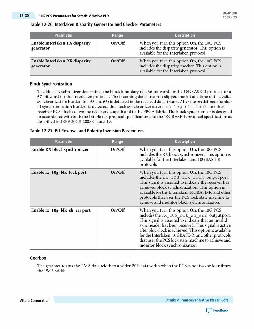
Table 12-26: Interlaken Disparity Generator and Checker Parameters
DescriptionRangeParameter
When you turn this option On, the 10G PCSincludes the disparity generator. This option isavailable for the Interlaken protocol.
On/OffEnable Interlaken TX disparitygenerator
When you turn this option On, the 10G PCSincludes the disparity checker. This option isavailable for the Interlaken protocol.
On/OffEnable Interlaken RX disparitygenerator
Block Synchronization
The block synchronizer determines the block boundary of a 66-bit word for the 10GBASE-R protocol or a67-bit word for the Interlaken protocol. The incoming data stream is slipped one bit at a time until a validsynchronization header (bits 65 and 66) is detected in the received data stream. After the predefined numberof synchronization headers is detected, the block synchronizer asserts rx_10g_blk_lock to otherreceiver PCS blocks down the receiver datapath and to the FPGA fabric. The block synchronizer is designedin accordance with both the Interlaken protocol specification and the 10GBASE-R protocol specification asdescribed in IEEE 802.3-2008 Clause-49.
Table 12-27: Bit Reversal and Polarity Inversion Parameters
DescriptionRangeParameter
When you turn this option On, the 10G PCSincludes the RX block synchronizer. This option isavailable for the Interlaken and 10GBASE-Rprotocols.
On/OffEnable RX block synchronizer
When you turn this option On, the 10G PCSincludes the rx_10G_blk_lock output port.This signal is asserted to indicate the receiver hasachieved block synchronization. This option isavailable for the Interlaken, 10GBASE-R, and otherprotocols that user the PCS lock state machine toachieve and monitor block synchronization.
On/OffEnable rx_10g_blk_lock port
When you turn this option On, the 10G PCSincludes therx_10G_blk_sh_err output port.This signal is asserted to indicate that an invalidsync header has been received. This signal is activeafter block lock is achieved. This option is availablefor the Interlaken, 10GBASE-R, and other protocolsthat user the PCS lock statemachine to achieve andmonitor block synchronization.
On/OffEnable rx_10g_blk_sh_err port
Gearbox
The gearbox adapts the PMA data width to a wider PCS data width when the PCS is not two or four timesthe PMA width.
Stratix V Transceiver Native PHY IP CoreAltera Corporation
Feedback
UG-0108010G PCS Parameters for Stratix V Native PHY12-30 2013.4.25

Table 12-28: Gearbox Parameters
DescriptionRangeParameter
When you turn this optionOn, the gearbox invertsthe polarity of TX data allowing you to correctincorrect placement and routing on the PCB.
On/OffEnable TX data polarity inversion
When you turn this option On, the TX gearboxoperates in bitslip mode.
On/OffEnable TX data bitslip
When you turn this optionOn, the gearbox invertsthe polarity of RX data allowing you to correctincorrect placement and routing on the PCB.
On/OffEnable RX data polarity inversion
When you turn this option On, the 10G PCS RXblock synchronizer operates in bitslip mode.
On/OffEnable RX data bitslip
When you turn this option On, the 10G PCSincludes the tx_10g_bitslip input port. Thedata slips 1 bit for every positive edge of the tx_10g_bitslip input. The maximum shift is <pcswidth> -1 bits, so that if the PCS is 64 bits wide,you can shift 0-63 bits.
On/OffEnable tx_10g_bitslip port
When you turn this option On, the 10G PCSincludes the rx_10g_bitslip input port. Thedata slips 1 bit for every positive edge of the rx_10g_bitslip input. he maximum shift is <pcswidth> -1 bits, so that if the PCS is 64 bits wide,you can shift 0-63 bits.
On/OffEnable rx_10g_bitslip port
Related InformationTransceiver Archictecture in Stratix V Devices
Interfaces for Stratix V Native PHYThis section describes the common, Standard and 10G PCS interfaces for the Stratix V Native PHY.
The Native PHY includes several interfaces that are common to all parameterizations. It also has separateinterfaces for the Standard and 10G PCS datapaths. If you use dynamic reconfiguration to change betweenthe Standard and 10G PCS datapaths, your top-level HDL file includes the port for both the Standard and10G PCS datapaths. In addition, the Native PHY allows you to enable ports, even for disabled blocks tofacilitate dynamic reconfiguration.
The Native PHY uses the following prefixes for port names:
• Standard PCS ports—tx_std_, rx_std_• 10G PCS ports—tx_10g_, rx_10g_• PMA ports—tx_pma_, rx_pma_
Altera CorporationStratix V Transceiver Native PHY IP Core
Feedback
12-31Interfaces for Stratix V Native PHYUG-010802013.4.25
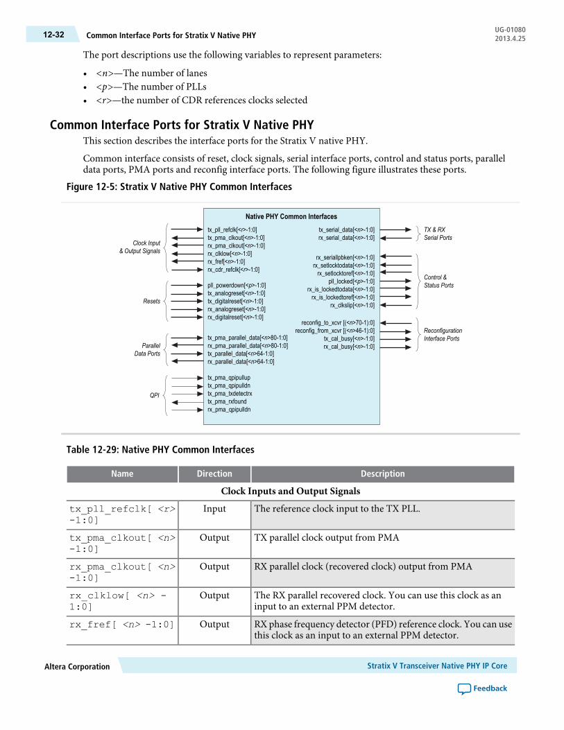
The port descriptions use the following variables to represent parameters:
• <n>—The number of lanes• <p>—The number of PLLs• <r>—the number of CDR references clocks selected
Common Interface Ports for Stratix V Native PHYThis section describes the interface ports for the Stratix V native PHY.
Common interface consists of reset, clock signals, serial interface ports, control and status ports, paralleldata ports, PMA ports and reconfig interface ports. The following figure illustrates these ports.
Figure 12-5: Stratix V Native PHY Common Interfaces
tx_pll_refclk[<r>-1:0]tx_pma_clkout[<n>-1:0]rx_pma_clkout[<n>-1:0]rx_clklow[<n>-1:0]rx_fref[<n>-1:0]rx_cdr_refclk[<r>-1:0]
Clock Input& Output Signals
rx_seriallpbken[<n>-1:0]rx_setlocktodata[<n>-1:0]rx_setlocktoref[<n>-1:0]
pll_locked[<p>-1:0]rx_is_lockedtodata[<n>-1:0]rx_is_lockedtoref[<n>-1:0]
rx_clkslip[<n>-1:0]
Control &Status Portspll_powerdown[<p>-1:0]
tx_analogreset[<n>-1:0]tx_digitalreset[<n>-1:0]rx_analogreset[<n>-1:0]rx_digitalreset[<n>-1:0]
Resets
QPI
tx_pma_parallel_data[<n>80-1:0]rx_pma_parallel_data[<n>80-1:0]tx_parallel_data[<n>64-1:0]rx_parallel_data[<n>64-1:0]
tx_pma_qpipulluptx_pma_qpipulldntx_pma_txdetectrxtx_pma_rxfoundrx_pma_qpipulldn
ParallelData Ports
tx_serial_data[<n>-1:0]rx_serial_data[<n>-1:0]
TX & RXSerial Ports
reconfig_to_xcvr [(<n>70-1):0]reconfig_from_xcvr [(<n>46-1):0]
tx_cal_busy[<n>-1:0]rx_cal_busy[<n>-1:0]
ReconfigurationInterface Ports
Native PHY Common Interfaces
Table 12-29: Native PHY Common Interfaces
DescriptionDirectionName
Clock Inputs and Output Signals
The reference clock input to the TX PLL.Inputtx_pll_refclk[ <r>-1:0]
TX parallel clock output from PMAOutputtx_pma_clkout[ <n>-1:0]
RX parallel clock (recovered clock) output from PMAOutputrx_pma_clkout[ <n>-1:0]
The RX parallel recovered clock. You can use this clock as aninput to an external PPM detector.
Outputrx_clklow[ <n> -1:0]
RX phase frequency detector (PFD) reference clock. You can usethis clock as an input to an external PPM detector.
Outputrx_fref[ <n> -1:0]
Stratix V Transceiver Native PHY IP CoreAltera Corporation
Feedback
UG-01080Common Interface Ports for Stratix V Native PHY12-32 2013.4.25

DescriptionDirectionName
Input reference clock for the RX PFD circuit.Inputrx_cdr_refclk[ <n>-1:0]
Resets
When asserted, resets the TX PLL. Active high, edge sensitivereset signal. By default, the Stratix V Native Transceiver PHY IPCores creates a separatepll_powerdown signal for each logicalPLL. However, the Fitter may merge the PLLs if they are in thesame transceiver bank. PLLs can only be merged if their pll_powerdown signals are driven from the same source. If the PLLsare in separate transceiver banks, you can choose to drive thepll_powerdown signals separately.
Inputpll_powerdown[ <n>-1:0]
When asserted, resets for TX PMA, TX clock generation block,and serializer. Active high, edge sensitive reset signal.
Inputtx_analogreset[<n> -1:0]
When asserted, resets the digital components of the TX datapath.Active high, edge sensitive reset signal.If your design includesbonded TX PCS channels, refer to Timing Constraints for ResetSignals when Using Bonded PCS Channels for a SDC constraintyou must include in your design.
Inputtx_digitalreset[<n> -1:0]
When asserted, resets the RXCDR, deserializer, Active high, edgesensitive reset signal.
Inputrx_analogreset[<n> -1:0]
When asserted, resets the digital components of the RX datapath.Active high, edge sensitive reset signal.
Inputrx_digitalreset[<n> -1:0]
Parallel Data Ports
TX parallel data for the PMA Direct datapath. Driven directlyfrom the FPGA fabric to the PMA. Not used when you enableeither the Standard or 10G PCS datapath.
Inputtx_pma_parallel_data[ <n> 80-1:0]
RX PMA parallel data driven from the PMA to the FPGA fabric.Not used when you enable either the Standard or 10G PCSdatapath.
Outputrx_pma_parallel_data[ <n> 80-1:0]
PCS TX parallel data. Used when you enable either the Standardor 10Gdatapath. For the Standard datapath, if you turn onEnablesimplified data interface , tx_parallel_data includes only the dataand control signals necessary for the current configuration.Dynamic reconfiguration of the interface is not supported. Forthe 10G PCS, if the parallel data interface is less than 64 bits wide,the low-order bits of tx_parallel_data are valid. For the 10G PCSoperating in 66:40 Basic mode, the 66 bus is formed as follows:{ tx_parallel_data[63:0],tx_10g_control[0], tx_10g_control[1]}.
Inputtx_parallel_data[<n> 64-1:0]
Altera CorporationStratix V Transceiver Native PHY IP Core
Feedback
12-33Common Interface Ports for Stratix V Native PHYUG-010802013.4.25

DescriptionDirectionName
PCS RX parallel data. Used when you enable either the Standardor 10Gdatapath. For the Standard datapath, if you turn onEnablesimplified data interface , rx_parallel_data includes only the dataand control signals necessary for the current configuration.Dynamic reconfiguration of the interface is not supported. Forthe 10G PCS, if the parallel data interface is less than 64 bits wide,the low-order bits of rx_parallel_data are valid. For the 10G PCSoperating in 66:40 mode, the 66 bus is formed as follows: {rx_parallel_data[63:0],rx_10g_control[0], rx_10g_control[1]}.
Outputrx_parallel_data[<n> 64-1:0]
QPI
QPI control input port. Only for QPI applications.Inputtx_pma_qpipullup
QPI control input port. Only for QPI applications.Inputtx_pma_qpipulldn
When asserted, the RX detect block in the TX PMA detects thepresence of a receiver at the other end of the channel. Afterreceiving a tx_pma_txdetectrx request, the receiver detectblock initiates the detection process. Only for QPI applications.
Inputtx_pma_txdetectrx
Indicates the status of an RX detection in the TX PMA. Only forQPI applications.
Outputtx_pma_rxfound
QPI control input port. Only for QPI applications.Inputrx_pma_qpipulldn
TX and RX Serial Ports
TX differential serial output data.Outputtx_serial_data[<n> -1:0]
RX differential serial output data.Inputrx_serial_data[<n> -1:0]
Control and Status Ports
When asserted, the transceiver enters loopback mode. Loopbackdrives TX data to the RX interface.
Inputrx_seriallpbken[<n> -1:0]
When asserted, programs the RX CDR to manual lock to datamode in which you control the reset sequence using the rx_setlocktoref and rx_setlocktodata. Refer to ResetSequence for CDR in Manual Lock Mode in Transceiver ResetControl in Stratix V Devices for more information about manualcontrol of the reset sequence.
Inputrx_set_locktodata[<n> -1:0]
Whenasserted, programs theRXCDR tomanual lock to referencemode in which you control the reset sequence using the rx_setlocktoref and rx_setlocktodata. Refer to ResetSequence for CDR in Manual Lock Mode in Transceiver ResetControl in Stratix V Devices for more information about manualcontrol of the reset sequence.
Inputrx_set_locktoref[<n> -1:0]
When asserted, indicates that the PLL is locked to the inputreference clock.
Outputpll_locked[ <p> -1:0]
Stratix V Transceiver Native PHY IP CoreAltera Corporation
Feedback
UG-01080Common Interface Ports for Stratix V Native PHY12-34 2013.4.25

DescriptionDirectionName
When asserted, the CDR is locked to the incoming data.Outputrx_is_lockedtodata[ <n>-1:0]
When asserted, the CDR is locked to the incoming referenceclock.
Outputrx_is_lockedtoref[<n> -1:0]
When asserted, the deserializer slips one clock edge. This signalis used to achieve word alignment.
Inputrx_clkslip[ <n> -1:0]
Reconfig Interface Ports
Reconfiguration signals from the Transceiver ReconfigurationController. <n> grows linearly with the number ofreconfiguration interfaces.
Inputreconfig_to_xcvr[( <n> 70-1):0]
Reconfiguration signals to the Transceiver ReconfigurationController. <n> grows linearly with the number ofreconfiguration interfaces.
Outputreconfig_from_xcvr[( <n> 46-1):0]
Reconfiguration status, indicates TX calibration is in progressOutputtx_cal_busy[ <n>-1:0]
Reconfiguration status, indicates RX calibration is in progressOutputrx_cal_busy[ <n>-1:0]
Related InformationTiming Constraints for Reset Signals when Using Bonded PCS Channels on page 17-10
Standard PCS Interface PortsThis section describes the PCS interface.
Figure 12-6: Standard PCS Interfaces
ClocksWordAligner
PhaseCompensation
FIFO
ByteOrdering
rx_std_rmfifo_empty[<n>-1:0]rx_std_rmfifo_full[<n>-1:0]
RateMatch FIFO
rx_std_polinv[<n>-1:0]tx_std_polinv[<n>-1:0]
PolarityInversion
PMAPorts
Standard PCS Interface Portsrx_std_bitrev_ena[<n>-1:0]
tx_std_bitslipboundarysel[5<n>-1:0]rx_std_bitslipboundarysel[5<n>-1:0]
rx_std_runlength_err[<n>-1:0]rx_std_wa_patternalign[<n>-1:0]
rx_std_comdet_ena[<n>-1:0]rx_std_wa_a1a2size[<n>-1:0]
rx_std_bitslip[<n>-1:0]
tx_std_elecidle[<n>-1:0]rx_std_signaldetect[<n>-1:0]rx_std_byterev_ena[<n>-1:0]Byte Serializer &
Deserializer
tx_std_clkout[<n>-1:0]rx_std_clkout[<n>-1:0]tx_std_coreclkin[<n>-1:0]rx_std_coreclkin[<n>-1:0]
rx_std_pcfifo_full[<n>-1:0]rx_std_pcfifo_empty[<n>-1:0]tx_std_pcfifo_full[<n>-1:0]tx_std_pcfifo_empty[<n>-1:0]
rx_std_byteorder_ena[<n>-1:0]rx_std_byteorder_flag[<n>-1:0]
Altera CorporationStratix V Transceiver Native PHY IP Core
Feedback
12-35Standard PCS Interface PortsUG-010802013.4.25
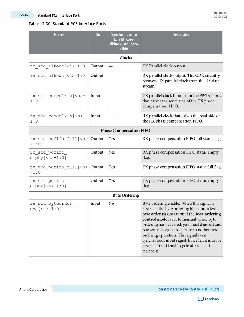
Table 12-30: Standard PCS Interface Ports
DescriptionSynchronous totx_std_core-
clkin/rx_std_core-clkin
DirName
Clocks
TX Parallel clock output.—Outputtx_std_clkout[<n>-1:0]
RX parallel clock output. The CDR circuitryrecovers RX parallel clock from the RX datastream.
—Outputrx_std_clkout[<n>-1:0]
TX parallel clock input from the FPGA fabricthat drives the write side of the TX phasecompensation FIFO.
—Inputtx_std_coreclkin[<n>-1:0]
RX parallel clock that drives the read side ofthe RX phase compensation FIFO.
—Inputrx_std_coreclkin[<n>-1:0]
Phase Compensation FIFO
RX phase compensation FIFO full status flag.YesOutputrx_std_pcfifo_full[<n>-1:0]
RX phase compensation FIFO status emptyflag.
YesOutputrx_std_pcfifo_empty[<n>-1:0]
TX phase compensation FIFO status full flag.YesOutputtx_std_pcfifo_full[<n>-1:0]
TX phase compensation FIFO status emptyflag.
YesOutputtx_std_pcfifo_empty[<n>-1:0]
Byte Ordering
Byte ordering enable. When this signal isasserted, the byte ordering block initiates abyte ordering operation if the Byte orderingcontrol mode is set to manual. Once byteordering has occurred, you must deassert andreassert this signal to perform another byteordering operation. This signal is ansynchronous input signal; however, it must beasserted for at least 1 cycle of rx_std_clkout.
NoInputrx_std_byteorder_ena[<n>-1:0]
Stratix V Transceiver Native PHY IP CoreAltera Corporation
Feedback
UG-01080Standard PCS Interface Ports12-36 2013.4.25
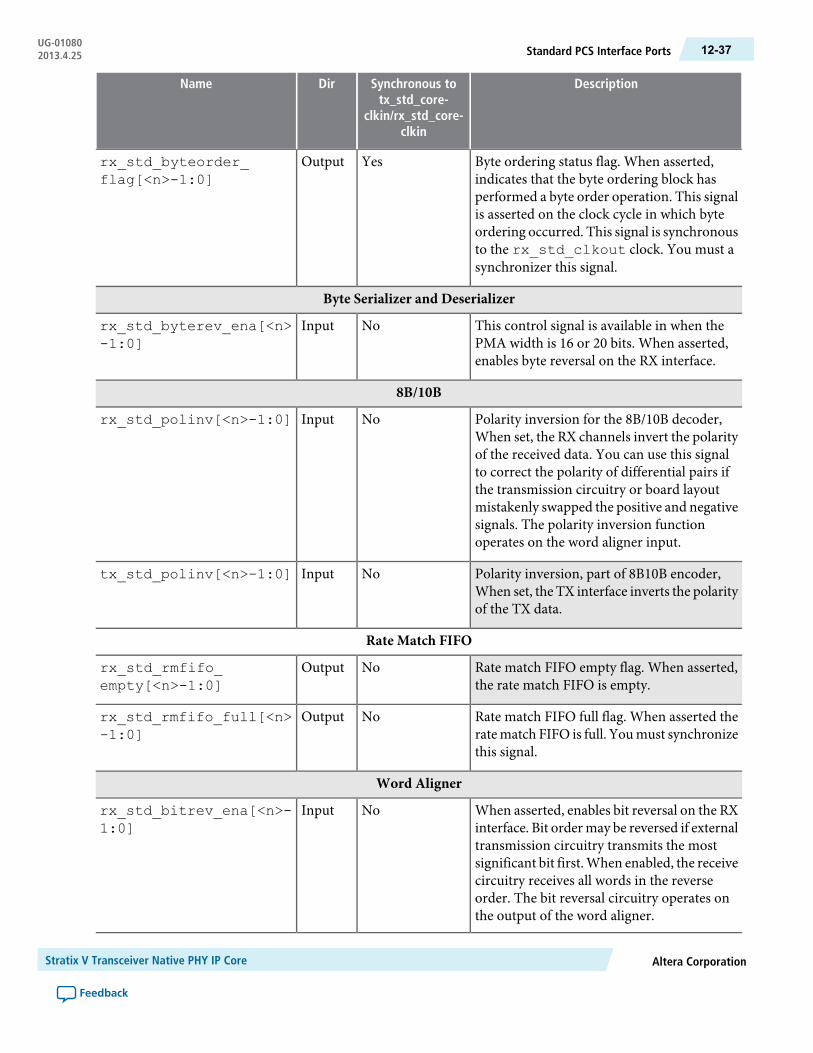
DescriptionSynchronous totx_std_core-
clkin/rx_std_core-clkin
DirName
Byte ordering status flag. When asserted,indicates that the byte ordering block hasperformed a byte order operation. This signalis asserted on the clock cycle in which byteordering occurred. This signal is synchronousto the rx_std_clkout clock. You must asynchronizer this signal.
YesOutputrx_std_byteorder_flag[<n>-1:0]
Byte Serializer and Deserializer
This control signal is available in when thePMA width is 16 or 20 bits. When asserted,enables byte reversal on the RX interface.
NoInputrx_std_byterev_ena[<n>-1:0]
8B/10B
Polarity inversion for the 8B/10B decoder,When set, the RX channels invert the polarityof the received data. You can use this signalto correct the polarity of differential pairs ifthe transmission circuitry or board layoutmistakenly swapped the positive and negativesignals. The polarity inversion functionoperates on the word aligner input.
NoInputrx_std_polinv[<n>-1:0]
Polarity inversion, part of 8B10B encoder,When set, the TX interface inverts the polarityof the TX data.
NoInputtx_std_polinv[<n>-1:0]
Rate Match FIFO
Rate match FIFO empty flag. When asserted,the rate match FIFO is empty.
NoOutputrx_std_rmfifo_empty[<n>-1:0]
Rate match FIFO full flag. When asserted theratematch FIFO is full. Youmust synchronizethis signal.
NoOutputrx_std_rmfifo_full[<n>-1:0]
Word Aligner
When asserted, enables bit reversal on the RXinterface. Bit order may be reversed if externaltransmission circuitry transmits the mostsignificant bit first.When enabled, the receivecircuitry receives all words in the reverseorder. The bit reversal circuitry operates onthe output of the word aligner.
NoInputrx_std_bitrev_ena[<n>-1:0]
Altera CorporationStratix V Transceiver Native PHY IP Core
Feedback
12-37Standard PCS Interface PortsUG-010802013.4.25

DescriptionSynchronous totx_std_core-
clkin/rx_std_core-clkin
DirName
BitSlip boundary selection signal. Specifies thenumber of bits that the TX bit slipper mustslip.
NoInputtx_std_bitslipboundarysel[5<n>-1:0]
This signal operates when the word aligner isin bitslip word alignment mode. It reports thenumber of bits that the RX block slipped toachieve deterministic latency.
NoOutputrx_std_bitslipboundarysel[5<n>-1:0]
When asserted, indicates a run lengthviolation. Asserted if the number ofconsecutive 1s or 0s exceeds the numberspecified in the parameter editor GUI.
NoOutputrx_std_runlength_err[<n>-1:0]
Active when you place the word aligner inmanual mode. In manual mode, you alignwords by asserting rx_st_wa_patternalign.rx_st_wa_patternalign is edge sensitive.
For more information refer to the WordAligner section in theTransceiver Architecturein Arria V Devices.
NoInputrx_st_wa_patternalign
Used for the SONET protocol. Assert whentheA1 andA2 framing bytesmust be detected.A1 and A2 are SONET backplane bytes andare only used when the PMA data width is 8bits.
NoInputrx_std_wa_a1a2size[<n>-1:0]
Usedwhenword alignermode is bitslipmode.For every rising edge of the rx_std_bitslip signal, theword boundary is shiftedby 1 bit. Each bitslip removes the earliestreceived bit from the received data. You mustsynchronize this signal.
NoInputrx_std_bitslip[<n>-1:0]
Miscellaneous
When asserted, enables a circuit to detect adownstream receiver. This signal must bedriven low when not in use because it causesthe TXPMA to enter electrical idlemodewiththe TX serial data signals in tristate mode.
Inputtx_std_elecidle[<n>-1:0]
Stratix V Transceiver Native PHY IP CoreAltera Corporation
Feedback
UG-01080Standard PCS Interface Ports12-38 2013.4.25

DescriptionSynchronous totx_std_core-
clkin/rx_std_core-clkin
DirName
Signal threshold detect indicator. Whenasserted, it indicates that the signal present atthe receiver input buffer is above theprogrammed signal detection threshold value.You must synchronize this signal.
NoOutputrx_std_signaldetect[<n>-1:0]
Related InformationTransceiver Architecture in Stratix V Devices
10G PCS InterfaceThe following figure illustrates the top-level signals of the 10G PCS. If you enable both the 10G PCS andStandard PCS your top-level HDL file includes all the interfaces for both.
Figure 12-7: Stratix V Native PHY 10G PCS Interfaces
Clocks
FrameGenerator
TX FIFO
RX FIFO
BlockSynchronizer
FrameSynchronizer
Bit-SlipGearboxFeature
64B/66B
BER
10G PCS Interface Ports
CRC32
tx_10g_coreclkin[<n>-1:0]rx_10g_coreclkin[<n>-1:0]tx_10g_clkout[<n>-1:0]rx_10g_clkout[<n>-1:0]rx_10g_clk33out[<n>-1:0]t
tx_10g_control[8<n>-1:0]tx_10g_data_valid[<n>-1:0]tx_10g_fifo_full[<n>-1:0]tx_10g_fifo_pfull[<n>-1:0]tx_10g_fifo_empty[<n>-1:0]tx_10g_fifo_pempt[<n>-1:0]ytx_10g_fifo_del[<n>-1:0]tx_10g_fifo_insert[<n>-1:0]
rx_10g_control[10<n>-1:0]rx_10g_fifo_rd_en[<n>-1:0]rx_10g_data_valid[<n>-1:0]rx_10g_fifo_full[<n>-1:0]rx_10g_fifo_pfull[<n>-1:0]rx_10g_fifo_empty[<n>-1:0]rx_10g_fifo_pempty[<n>-1:0]rx_10g_fifo_align_clr[<n>-1:0]rx_10g_fifo_align_en[<n>-1:0]rx_10g_align_val[<n>-1:0]rx_10g_fifo_del[<n>-1:0]rx_10g_fifo_insert[<n>-1:0]
rx_10g_crc32err[<n>-1:0]
tx_10g_diag_status[2<n>-1:0]tx_10g_burst_en[<n>-1:0]
tx_10g_frame[<n>-1:0]
rx_10g_frame[<n>-1:0]rx_10g_frame_lock[<n>-1:0]
rx_10g_pyld_ins[<n>-1:0]rx_10g_frame_mfrm_err[<n>-1:0]rx_10g_frame_sync_err[<n>-1:0]
rx_10g_scram_err[<n>-1:0]rx_10g_frame_skip_ins[<n>-1:0]rx_10g_frame_skip_err[<n>-1:0]rx_10g_frame_diag_err[<n>-1:0]
rx_10g_frame_diag_status[2<n>-1:0]
rx_10g_blk_lock[<n>-1:0]rx_10g_blk_sh_err[<n>-1:0]
rx_10g_bitslip[<n>-1:0]tx_10g_bitslip[7<n>-1:0]
rx_10g_clr_errblk_count[<n>-1:0]
rx_10g_highber[<n>-1:0]rx_10g_clr_highber_cnt[<n>-1:0]
The following table describes the signals available for the 10G PCS datapath. When you enable both the 10Gand Standard datapaths, both sets of signals are included in the top-level HDL file for the Native PHY.
In the following table, the column labeled “Synchronous to tx_10_coreclkin/rx_10g_coreclkin” refersto cases where the phase compensation FIFO is not in register mode.
Note:
Altera CorporationStratix V Transceiver Native PHY IP Core
Feedback
12-3910G PCS InterfaceUG-010802013.4.25
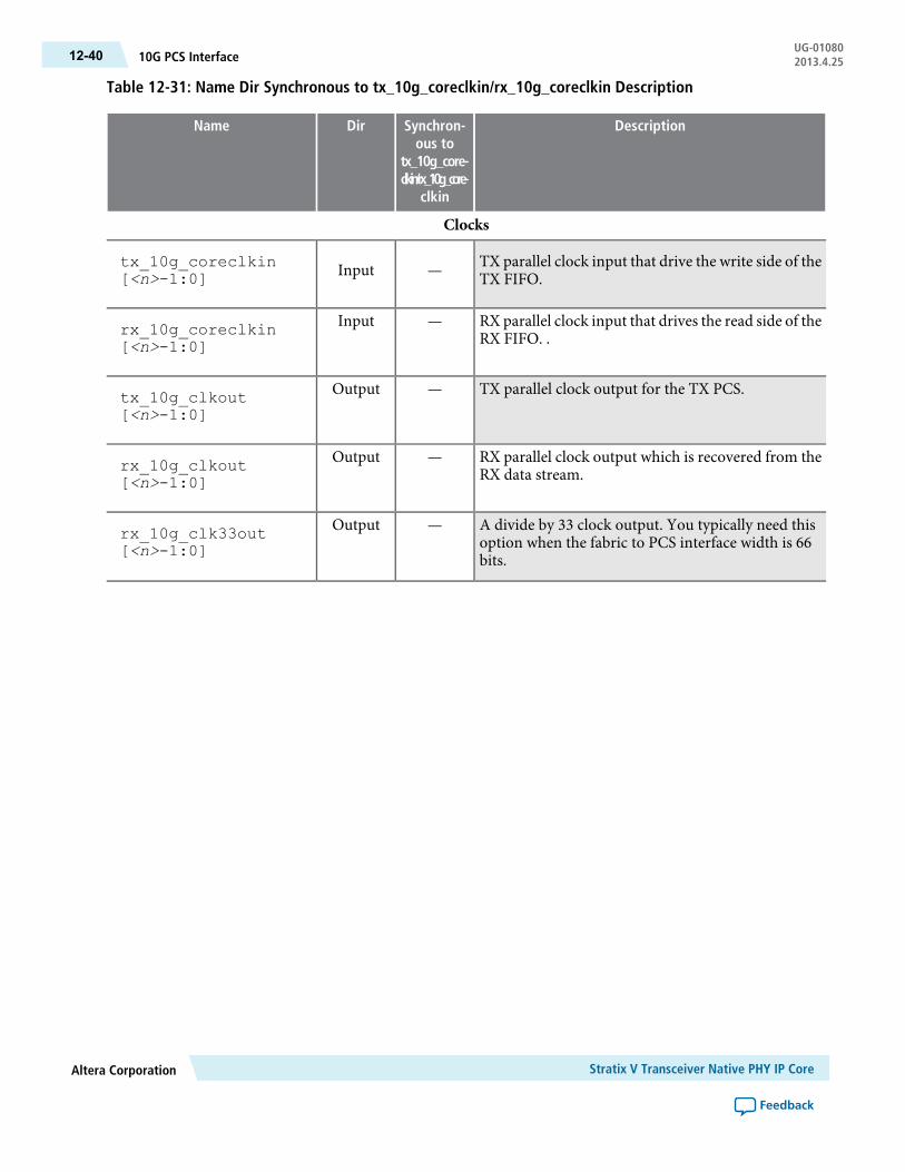
Table 12-31: Name Dir Synchronous to tx_10g_coreclkin/rx_10g_coreclkin Description
DescriptionSynchron-ous to
tx_10g_core-clkin/rx_10g_core-
clkin
DirName
Clocks
TX parallel clock input that drive the write side of theTX FIFO.—Inputtx_10g_coreclkin
[<n>-1:0]
RX parallel clock input that drives the read side of theRX FIFO. .
—Inputrx_10g_coreclkin[<n>-1:0]
TX parallel clock output for the TX PCS.—Outputtx_10g_clkout[<n>-1:0]
RX parallel clock output which is recovered from theRX data stream.
—Outputrx_10g_clkout[<n>-1:0]
A divide by 33 clock output. You typically need thisoption when the fabric to PCS interface width is 66bits.
—Outputrx_10g_clk33out[<n>-1:0]
Stratix V Transceiver Native PHY IP CoreAltera Corporation
Feedback
UG-0108010G PCS Interface12-40 2013.4.25
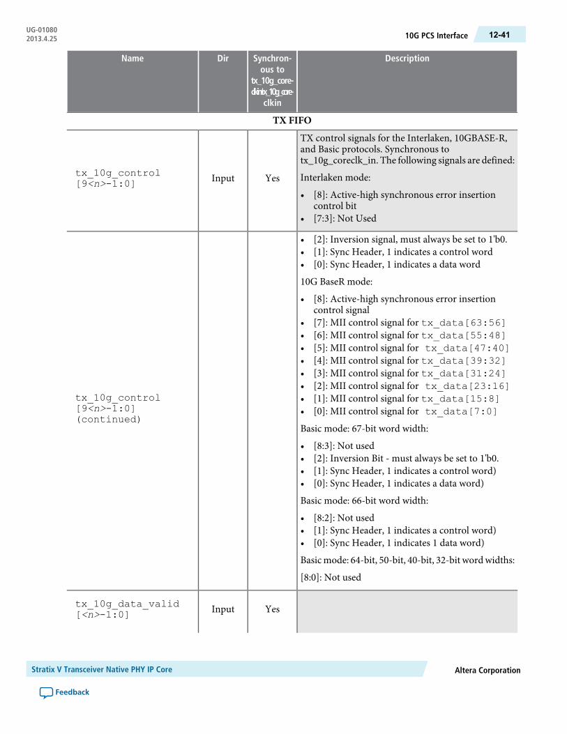
DescriptionSynchron-ous to
tx_10g_core-clkin/rx_10g_core-
clkin
DirName
TX FIFO
TX control signals for the Interlaken, 10GBASE-R,and Basic protocols. Synchronous totx_10g_coreclk_in. The following signals are defined:
Interlaken mode:
• [8]: Active-high synchronous error insertioncontrol bit
• [7:3]: Not Used
YesInputtx_10g_control[9<n>-1:0]
• [2]: Inversion signal, must always be set to 1'b0.• [1]: Sync Header, 1 indicates a control word• [0]: Sync Header, 1 indicates a data word
10G BaseR mode:
• [8]: Active-high synchronous error insertioncontrol signal
• [7]: MII control signal for tx_data[63:56]• [6]: MII control signal for tx_data[55:48]• [5]: MII control signal for tx_data[47:40]• [4]: MII control signal for tx_data[39:32]• [3]: MII control signal for tx_data[31:24]• [2]: MII control signal for tx_data[23:16]• [1]: MII control signal for tx_data[15:8]• [0]: MII control signal for tx_data[7:0]
Basic mode: 67-bit word width:
• [8:3]: Not used• [2]: Inversion Bit - must always be set to 1'b0.• [1]: Sync Header, 1 indicates a control word)• [0]: Sync Header, 1 indicates a data word)
Basic mode: 66-bit word width:
• [8:2]: Not used• [1]: Sync Header, 1 indicates a control word)• [0]: Sync Header, 1 indicates 1 data word)
Basicmode: 64-bit, 50-bit, 40-bit, 32-bit wordwidths:
[8:0]: Not used
tx_10g_control[9<n>-1:0](continued)
YesInputtx_10g_data_valid[<n>-1:0]
Altera CorporationStratix V Transceiver Native PHY IP Core
Feedback
12-4110G PCS InterfaceUG-010802013.4.25

DescriptionSynchron-ous to
tx_10g_core-clkin/rx_10g_core-
clkin
DirName
When asserted, indicates if tx_data is valid Use ofthis signal depends upon the protocol you areimplementing, as follows:
• 10G BASE-R: Tie to 1'b1• Interlaken: Acts as control for FIFO write enable.
You should tie this signal to tx_10g_fifo_pempty.
• Basic with phase compensation FIFO: Tie to 1'b1as long as tx_coreclkin = data_rate/pld_pcs interface width. Otherwise, tiethis signal to tx_10g_fifo_pempty.
• Basic with phase compensation FIFO in registermode. This mode only allows a 1:1 gear box ratiosuch as 32:32 and 64:64; consequently, you can tietx_10g_data_valid to 1’b1.
When asserted, indicates that the TX FIFO is full.Synchronous to tx_10g_coreclkin.
YesOutputtx_10g_fifo_full[<n>-1:0]
When asserted, indicates that the TXFIFO is partiallyfull. Synchronous to tx_10g_coreclkin.
YesOutputtx_10g_fifo_pfull[<n>-1:0]
TX FIFO empty flag. Synchronous to tx_10g_clkout. This signal is pulse-stretched; you must usea synchronizer.
NoOutputtx_10g_fifo_empty[<n>-1:0]
TX FIFO partially empty flag. Synchronous to tx_10g_clkout. This signal is pulse-stretched; youmust use a synchronizer.
NoOutputtx_10g_fifo_pempty[<n>-1:0]
When asserted, indicates that a word has been deletedfrom the rate match FIFO. This signal is used for the10GBASE-R protocol.
YesOutputtx_10g_fifo_del[<n>-1:0]
When asserted, indicates that aword has been insertedinto the rate match FIFO. This signal is used for the10GBASE-R protocol. This signal is pulse-stretched,you must use a synchronizer.
NoOutputtx_10g_fifo_insert[<n>-1:0]
Stratix V Transceiver Native PHY IP CoreAltera Corporation
Feedback
UG-0108010G PCS Interface12-42 2013.4.25

DescriptionSynchron-ous to
tx_10g_core-clkin/rx_10g_core-
clkin
DirName
RX FIFO
YesOutputrx_10g_control[10<n>-1:0]
Altera CorporationStratix V Transceiver Native PHY IP Core
Feedback
12-4310G PCS InterfaceUG-010802013.4.25
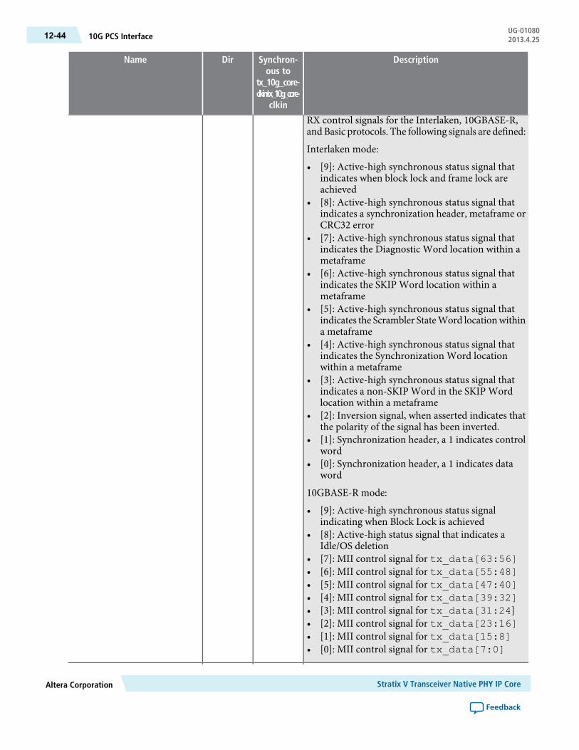
DescriptionSynchron-ous to
tx_10g_core-clkin/rx_10g_core-
clkin
DirName
RX control signals for the Interlaken, 10GBASE-R,and Basic protocols. The following signals are defined:
Interlaken mode:
• [9]: Active-high synchronous status signal thatindicates when block lock and frame lock areachieved
• [8]: Active-high synchronous status signal thatindicates a synchronization header, metaframe orCRC32 error
• [7]: Active-high synchronous status signal thatindicates the Diagnostic Word location within ametaframe
• [6]: Active-high synchronous status signal thatindicates the SKIP Word location within ametaframe
• [5]: Active-high synchronous status signal thatindicates the Scrambler StateWord locationwithina metaframe
• [4]: Active-high synchronous status signal thatindicates the Synchronization Word locationwithin a metaframe
• [3]: Active-high synchronous status signal thatindicates a non-SKIP Word in the SKIP Wordlocation within a metaframe
• [2]: Inversion signal, when asserted indicates thatthe polarity of the signal has been inverted.
• [1]: Synchronization header, a 1 indicates controlword
• [0]: Synchronization header, a 1 indicates dataword
10GBASE-R mode:
• [9]: Active-high synchronous status signalindicating when Block Lock is achieved
• [8]: Active-high status signal that indicates aIdle/OS deletion
• [7]: MII control signal for tx_data[63:56]• [6]: MII control signal for tx_data[55:48]• [5]: MII control signal for tx_data[47:40]• [4]: MII control signal for tx_data[39:32]• [3]: MII control signal for tx_data[31:24]• [2]: MII control signal for tx_data[23:16]• [1]: MII control signal for tx_data[15:8]• [0]: MII control signal for tx_data[7:0]
Stratix V Transceiver Native PHY IP CoreAltera Corporation
Feedback
UG-0108010G PCS Interface12-44 2013.4.25

DescriptionSynchron-ous to
tx_10g_core-clkin/rx_10g_core-
clkin
DirName
rx_10g_control[10<n>-1:0](continued)
Basic mode: 67-bit mode with Block Sync:
• [9]: Active-high synchronous status signal thatindicates when Block Lock is achieved.
• [8]: Active-high synchronous status signal thatindicates a sync header error
• [7:3]: Not used [2]: Used• [1]: Synchronization header, a 1 indicates control
word• [0]: Synchronization header, a 1 indicates data
word
Basic mode: 66-bit mode with Block Sync:
[9]: Active-high synchronous status signal thatindicates when Block Lock is achieved.
[8]: Active-high synchronous status signal thatindicates a sync header error.
[7:2]: Not used
• [1]: Synchronization header, a 1 indicates controlword
• [0]: Synchronization header, a 1 indicates dataword
Basic mode: 67-bit mode without Block Sync:
[9:3]: Not used
66-bit mode without Block Sync:
[9:2]: Not used
• [1]: Synchronization header, a 1 indicates controlword
• [0]: Synchronization header, a 1 indicates dataword
Basic mode: 64-bit, 50-bit, 40-bit and 32-bit modes:
[9:0]: Not used
Active high read enable signal for RXFIFO.Assertingthis signal reads 1 word from the RX FIFO.
YesInputrx_10g_fifo_rd_en[<n>-1:0]
YesOutputrx_10g_data_valid[<n>-1:0]
Altera CorporationStratix V Transceiver Native PHY IP Core
Feedback
12-4510G PCS InterfaceUG-010802013.4.25
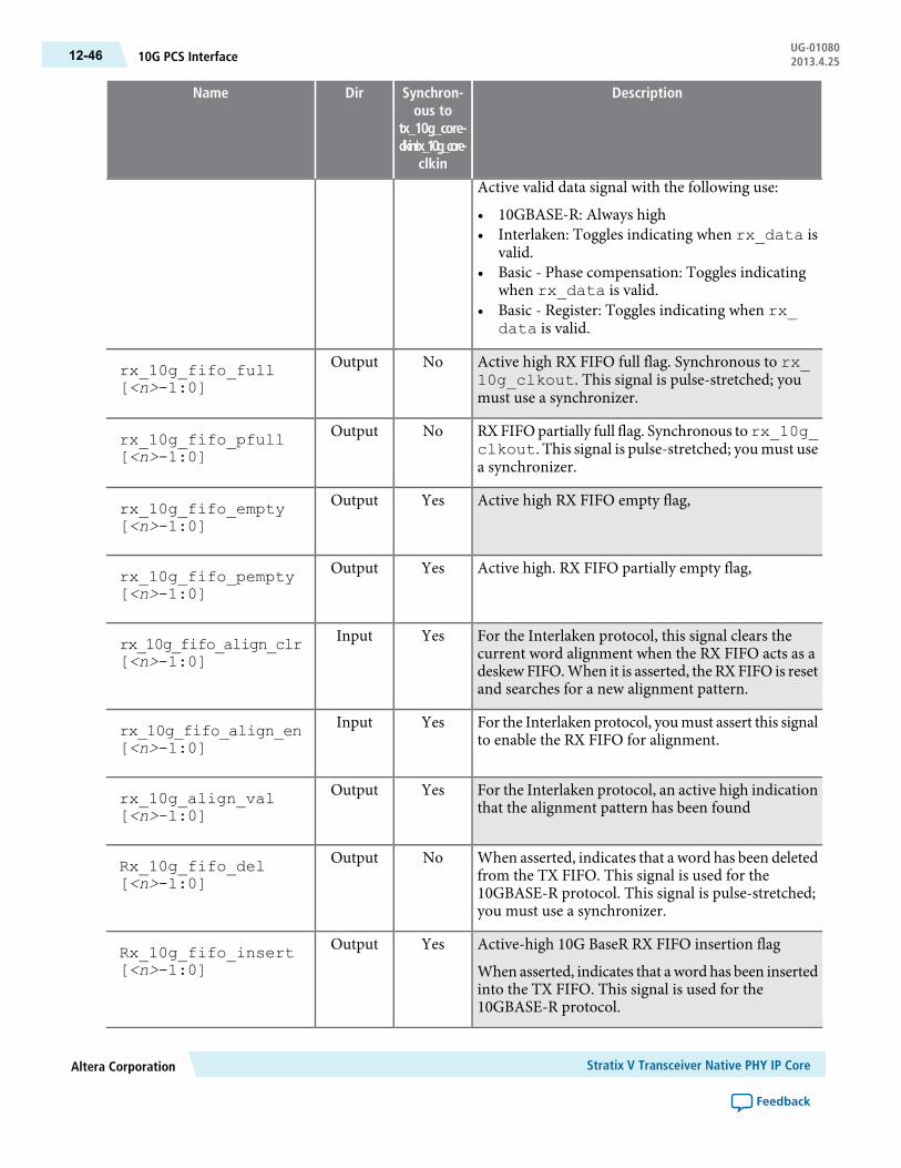
DescriptionSynchron-ous to
tx_10g_core-clkin/rx_10g_core-
clkin
DirName
Active valid data signal with the following use:
• 10GBASE-R: Always high• Interlaken: Toggles indicating when rx_data is
valid.• Basic - Phase compensation: Toggles indicating
when rx_data is valid.• Basic - Register: Toggles indicating when rx_
data is valid.
Active high RX FIFO full flag. Synchronous to rx_10g_clkout. This signal is pulse-stretched; youmust use a synchronizer.
NoOutputrx_10g_fifo_full[<n>-1:0]
RXFIFOpartially full flag. Synchronous torx_10g_clkout. This signal is pulse-stretched; you must usea synchronizer.
NoOutputrx_10g_fifo_pfull[<n>-1:0]
Active high RX FIFO empty flag,YesOutputrx_10g_fifo_empty[<n>-1:0]
Active high. RX FIFO partially empty flag,YesOutputrx_10g_fifo_pempty[<n>-1:0]
For the Interlaken protocol, this signal clears thecurrent word alignment when the RX FIFO acts as adeskewFIFO.When it is asserted, the RXFIFO is resetand searches for a new alignment pattern.
YesInputrx_10g_fifo_align_clr[<n>-1:0]
For the Interlaken protocol, youmust assert this signalto enable the RX FIFO for alignment.
YesInputrx_10g_fifo_align_en[<n>-1:0]
For the Interlaken protocol, an active high indicationthat the alignment pattern has been found
YesOutputrx_10g_align_val[<n>-1:0]
When asserted, indicates that a word has been deletedfrom the TX FIFO. This signal is used for the10GBASE-R protocol. This signal is pulse-stretched;you must use a synchronizer.
NoOutputRx_10g_fifo_del[<n>-1:0]
Active-high 10G BaseR RX FIFO insertion flag
When asserted, indicates that aword has been insertedinto the TX FIFO. This signal is used for the10GBASE-R protocol.
YesOutputRx_10g_fifo_insert[<n>-1:0]
Stratix V Transceiver Native PHY IP CoreAltera Corporation
Feedback
UG-0108010G PCS Interface12-46 2013.4.25
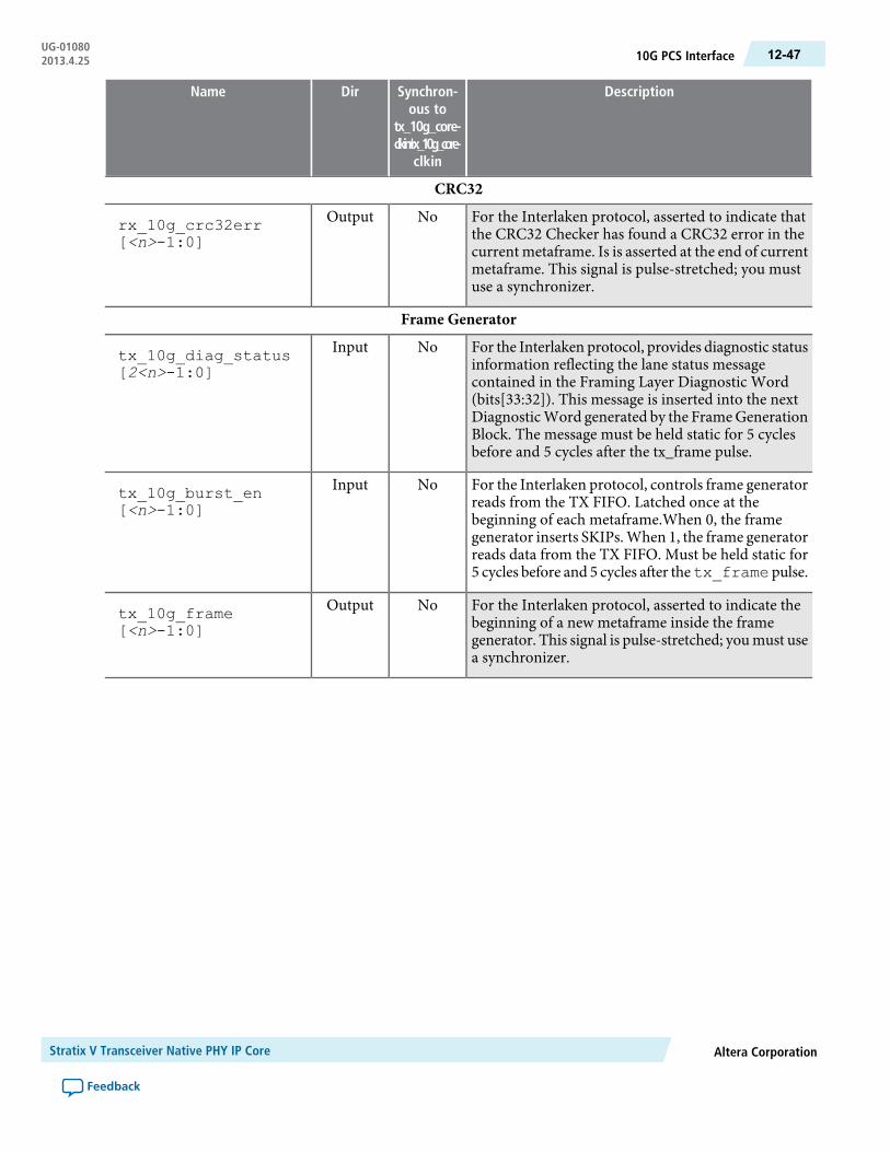
DescriptionSynchron-ous to
tx_10g_core-clkin/rx_10g_core-
clkin
DirName
CRC32
For the Interlaken protocol, asserted to indicate thatthe CRC32 Checker has found a CRC32 error in thecurrent metaframe. Is is asserted at the end of currentmetaframe. This signal is pulse-stretched; you mustuse a synchronizer.
NoOutputrx_10g_crc32err[<n>-1:0]
Frame Generator
For the Interlaken protocol, provides diagnostic statusinformation reflecting the lane status messagecontained in the Framing Layer Diagnostic Word(bits[33:32]). This message is inserted into the nextDiagnosticWord generated by the FrameGenerationBlock. The message must be held static for 5 cyclesbefore and 5 cycles after the tx_frame pulse.
NoInputtx_10g_diag_status[2<n>-1:0]
For the Interlaken protocol, controls frame generatorreads from the TX FIFO. Latched once at thebeginning of each metaframe.When 0, the framegenerator inserts SKIPs. When 1, the frame generatorreads data from the TX FIFO. Must be held static for5 cycles before and 5 cycles after thetx_frame pulse.
NoInputtx_10g_burst_en[<n>-1:0]
For the Interlaken protocol, asserted to indicate thebeginning of a new metaframe inside the framegenerator. This signal is pulse-stretched; youmust usea synchronizer.
NoOutputtx_10g_frame[<n>-1:0]
Altera CorporationStratix V Transceiver Native PHY IP Core
Feedback
12-4710G PCS InterfaceUG-010802013.4.25
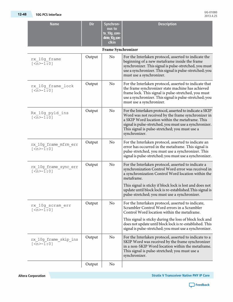
DescriptionSynchron-ous to
tx_10g_core-clkin/rx_10g_core-
clkin
DirName
Frame Synchronizer
For the Interlaken protocol, asserted to indicate thebeginning of a new metaframe inside the framesynchronizer. This signal is pulse-stretched, you mustuse a synchronizer. This signal is pulse-stretched; youmust use a synchronizer.
NoOutputrx_10g_frame[<n>-1:0]
For the Interlaken protocol, asserted to indicate thatthe frame synchronizer state machine has achievedframe lock. This signal is pulse-stretched, you mustuse a synchronizer. This signal is pulse-stretched; youmust use a synchronizer.
NoOutputrx_10g_frame_lock[<n>-1:0]
For the Interlaken protocol, asserted to indicate a SKIPWord was not received by the frame synchronizer ina SKIP Word location within the metaframe. Thissignal is pulse-stretched, youmust use a synchronizer.This signal is pulse-stretched; you must use asynchronizer.
NoOutputRx_10g_pyld_ins[<n>-1:0]
For the Interlaken protocol, asserted to indicate anerror has occurred in the metaframe. This signal ispulse-stretched, you must use a synchronizer. Thissignal is pulse-stretched; youmust use a synchronizer.
NoOutputrx_10g_frame_mfrm_err[<n>-1:0]
For the Interlaken protocol, asserted to indicate asynchronization Control Word error was received ina synchronization Control Word location within themetaframe.
This signal is sticky if block lock is lost and does notupdate until block lock is re-established.This signal ispulse-stretched; you must use a synchronizer.
NoOutputrx_10g_frame_sync_err[<n>-1:0]
For the Interlaken protocol, asserted to indicate,Scrambler Control Word errors in a ScramblerControl Word location within the metaframe.
This signal is sticky during the loss of block lock anddoes not update until block lock is re-established. Thissignal is pulse-stretched; youmust use a synchronizer.
NoOutputrx_10g_scram_err[<n>-1:0]
For the Interlaken protocol, asserted to indicate to aSKIP Word was received by the frame synchronizerin a non-SKIP Word location within the metaframe.This signal is pulse-stretched; you must use asynchronizer.
NoOutputrx_10g_frame_skip_ins[<n>-1:0]
NoOutput
Stratix V Transceiver Native PHY IP CoreAltera Corporation
Feedback
UG-0108010G PCS Interface12-48 2013.4.25

DescriptionSynchron-ous to
tx_10g_core-clkin/rx_10g_core-
clkin
DirName
rx_10g_frame_skip_err[<n>-1:0]
For the Interlaken protocol, asserted to indicate a SkipControl Word error was received in a Skip ControlWord location within the metaframe.
This signal is sticky during the loss of block lock anddoes not update until block lock is re-established. Thissignal is pulse-stretched; youmust use a synchronizer.
For the Interlaken protocol, asserted to indicate aDiagnostic Control Word error was received in aDiagnostic Control Word location within themetaframe.
This signal is sticky during the loss of block lock anddoes not update until block lock is re-established. Thissignal is pulse-stretched; youmust use a synchronizer.
NoOutputrx_10g_frame_diag_err[<n>-1:0]
For the Interlaken protocol, reflects the lane statusmessage contained in the framing layer DiagnosticWord (bits[33:32]). This information is latched whena valid Diagnostic Word is received in a DiagnosticWord Metaframe location. This signal ispulse-stretched; you must use a synchronizer.
NoOutputrx_10g_frame_diag_status[2<n>-1:0]
Block Synchronizer
Active-high status signal that is asserted when blocksynchronizer acquires block lock. Valid for the10GBASE-R and Interlaken protocols, and any basicmode that uses the lock state machine to achieve andmonitor block synchronization for word alignment.Once the block synchronizer acquires block lock, ittakes at least 16 errors for rx_10g_blk_lock tobe deasserted.
NoOutputrx_10g_blk_lock[<n>-1:0]
Error status signal fromblock synchronizer indicatingan invalid synchronization header has been received.Valid for the 10GBASE-R and Interlaken protocols,and any legal basic mode that uses the lock statemachine to achieve and monitor blocksynchronization for word alignment. Active only afterblock lock is achieved. This signal is pulse-stretched;you must use a synchronizer.
NoOutputrx_10g_blk_sh_err[<n>-1:0]
Altera CorporationStratix V Transceiver Native PHY IP Core
Feedback
12-4910G PCS InterfaceUG-010802013.4.25

DescriptionSynchron-ous to
tx_10g_core-clkin/rx_10g_core-
clkin
DirName
Bit-Slip Gearbox Feature Synchronizer
User control bit-slip in the RX Gearbox. Slips one bitper rising edge pulse.
NoInputrx_10g_bitslip[<n>-1:0]
TX bit-slip is controlled by tx_bitslip port.
Shifts the number of bit location specified by tx_bitslip. The maximum shift is <pcswidth-1>.
NoInputtx_10g_bitslip[7<n>-1:0]
64b/66b
For the 10GBASE-R protocol, asserted to clear theerror block counter which counts the number of timesthe RX state machine enters the RX error state.
NoInputrx_10g_clr_errblk_count[<n>-1:0]
BER
For the 10GBASE-R protocol, status signal assertedto indicate a bit error ratio of >10–4. A count of 16 in125us indicates a bit error ratio of >10–4. Onceasserted, it remains high for at least 125 us.
NoOutputrx_10g_highber[<n>-1:0]
For the 10GBASE-R protocol, status signal assertedto clear the BER counter which counts the number oftimes theBER statemachine enters the BER_BAD_SHstate. This signal has no effect on the operation of theBER state machine.
NoInputrx_10g_clr_highber_cnt[<n>-1:0]
SDC Timing Constraints of Stratix V Native PHYThis section describes SDC examples and approaches to identify false timing paths.
The Quartus II 12.1 software reports timing violations for asynchronous inputs to the Standard PCS and10G PCS. Because many violations are for asynchronous paths, they do not represent actual timing failures.You may choose one of the following three approaches to identify these false timing paths to the Quartus IIor TimeQuest software.
In all of these examples, you must substitute you actual signal names for the signal names shown.
Example 12-1: Using the set_false_path Constraint to Identify Asynchronous Inputs
You can cut these paths in your Synopsys Design Constraints (.sdc) file by using the set_false_pathcommand as shown in following example.
set_false_path -through {*10gtxbursten*} -to [get_registers*10g_tx_pcs*SYNC_DATA_REG*]
Stratix V Transceiver Native PHY IP CoreAltera Corporation
Feedback
UG-01080SDC Timing Constraints of Stratix V Native PHY12-50 2013.4.25

set_false_path -through {*10gtxdiagstatus*} -to [get_registers*10g_tx_pcs*SYNC_DATA_REG*]
set_false_path -through {*10gtxwordslip*} -to [get_registers*10g_tx_pcs*SYNC_DATA_REG*]
set_false_path -through {*10gtxbitslip*} -to [get_registers*10g_tx_pcs*SYNC_DATA_REG*]
set_false_path -through {*10grxbitslip*} -to [get_registers*10g_rx_pcs*SYNC_DATA_REG*]
set_false_path -through {*10grxclrbercount*} -to [get_registers*10g_rx_pcs*SYNC_DATA_REG*]
set_false_path -through {*10grxclrerrblkcnt*} -to [get_registers*10g_rx_pcs*SYNC_DATA_REG*]set_false_path -through {*10grxprbserrclr*} -to [get_registers*10g_rx_pcs*SYNC_DATA_REG*]
set_false_path -through {*8gbitslip*} -to [get_registers*8g_rx_pcs*SYNC_DATA_REG*]set_false_path -through {*8gbytordpld*} -to [get_registers*8g_rx_pcs*SYNC_DATA_REG*]set_false_path -through {*8gcmpfifoburst*} -to [get_registers*8g_rx_pcs*SYNC_DATA_REG*]set_false_path -through {*8gphfifoburstrx*} -to [get_registers*8g_rx_pcs*SYNC_DATA_REG*]
set_false_path -through {*8gsyncsmen*} -to [get_registers*8g*pcs*SYNC_DATA_REG*]set_false_path -through {*8gwrdisablerx*} -to [get_registers*8g_rx_pcs*SYNC_DATA_REG*]set_false_path -through {*rxpolarity*} -to [get_registers*SYNC_DATA_REG*]set_false_path -through {*pldeidleinfersel*} -to [get_registers*SYNC_DATA_REG*]
Example 12-2: Using the max_delay Constraint to Identify Asynchronous Inputs
You can use the set_max_delay constraint on a given path to create a constraint for asynchronoussignals that do not have a specific clock relationship but require amaximumpath delay. The followingexample illustrates this approach.
# Example: Apply 10ns max delay
set_max_delay -from *tx_from_fifo* -to *8g*pcs*SYNC_DATA_REG1 10
Altera CorporationStratix V Transceiver Native PHY IP Core
Feedback
12-51SDC Timing Constraints of Stratix V Native PHYUG-010802013.4.25
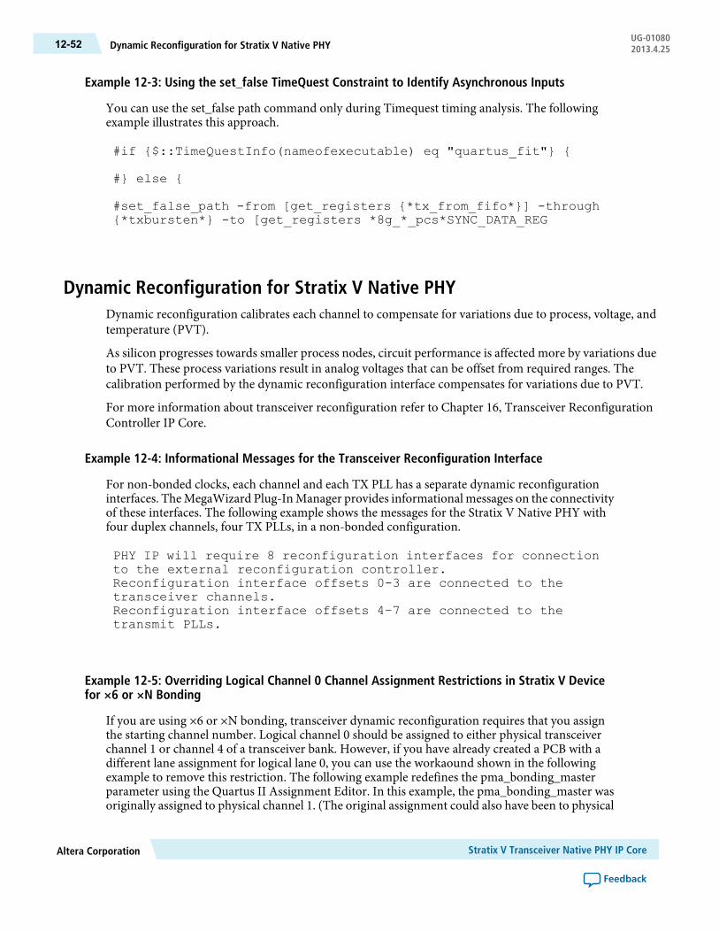
Example 12-3: Using the set_false TimeQuest Constraint to Identify Asynchronous Inputs
You can use the set_false path command only during Timequest timing analysis. The followingexample illustrates this approach.
#if {$::TimeQuestInfo(nameofexecutable) eq "quartus_fit"} {
#} else {
#set_false_path -from [get_registers {*tx_from_fifo*}] -through{*txbursten*} -to [get_registers *8g_*_pcs*SYNC_DATA_REG
Dynamic Reconfiguration for Stratix V Native PHYDynamic reconfiguration calibrates each channel to compensate for variations due to process, voltage, andtemperature (PVT).
As silicon progresses towards smaller process nodes, circuit performance is affected more by variations dueto PVT. These process variations result in analog voltages that can be offset from required ranges. Thecalibration performed by the dynamic reconfiguration interface compensates for variations due to PVT.
For more information about transceiver reconfiguration refer to Chapter 16, Transceiver ReconfigurationController IP Core.
Example 12-4: Informational Messages for the Transceiver Reconfiguration Interface
For non-bonded clocks, each channel and each TX PLL has a separate dynamic reconfigurationinterfaces. The MegaWizard Plug-In Manager provides informational messages on the connectivityof these interfaces. The following example shows the messages for the Stratix V Native PHY withfour duplex channels, four TX PLLs, in a non-bonded configuration.
PHY IP will require 8 reconfiguration interfaces for connectionto the external reconfiguration controller.Reconfiguration interface offsets 0-3 are connected to thetransceiver channels.Reconfiguration interface offsets 4–7 are connected to thetransmit PLLs.
Example 12-5: Overriding Logical Channel 0 Channel Assignment Restrictions in Stratix V Devicefor ×6 or ×N Bonding
If you are using ×6 or ×N bonding, transceiver dynamic reconfiguration requires that you assignthe starting channel number. Logical channel 0 should be assigned to either physical transceiverchannel 1 or channel 4 of a transceiver bank. However, if you have already created a PCB with adifferent lane assignment for logical lane 0, you can use the workaound shown in the followingexample to remove this restriction. The following example redefines the pma_bonding_masterparameter using the Quartus II Assignment Editor. In this example, the pma_bonding_master wasoriginally assigned to physical channel 1. (The original assignment could also have been to physical
Stratix V Transceiver Native PHY IP CoreAltera Corporation
Feedback
UG-01080Dynamic Reconfiguration for Stratix V Native PHY12-52 2013.4.25
channel 4.) The to parameter reassigns the pma_bonding_master to the Deterministic Latency PHYinstance name. You must substitute the instance name from your design for the instance nameshown in quotation marks
set_parameter -name pma_bonding_master "\"1\"" -to "<PHY IPinstance name>"
Simulation SupportThe Quartus II 12.1 release provides simulation and compilation support for the Stratix V Native PHY IPCore. Refer to Running a Simulation Testbench for a description of the directories and files that the QuartusII software creates automatically when you generate your Stratix V Transceiver Native PHY IP Core.
Altera CorporationStratix V Transceiver Native PHY IP Core
Feedback
12-53Simulation SupportUG-010802013.4.25
13Arria V Transceiver Native PHY IP Core
2013.4.25UG-01080 Subscribe Feedback
The Arria V Transceiver Native PHY IP Core provides direct access to all control and status signals of thetransceiver channels. Unlike other PHY IP Cores, the Native PHY IP Core does not include an AvalonMemory-Mapped (Avalon-MM) interface. Instead, it exposes all signals directly as ports. The Arria VTransceiver Native PHY IP Core provides the following datapaths:
• Standard PCS—When you enable the Standard PCS, you can select the PCS functions and control andstatus ports that your transceiver PHY requires.
• PMA Direct—When you select PMA Direct mode, the Native PHY provides direct access to the PMAfrom the FPGA fabric; consequently, the latency for transmitted and received data is lower. However,you must implement any PCS function that your design requires in the FPGA fabric.
The Native Transceiver PHY does not include an embedded reset controller. You can either design customreset logic or incorporate Altera’s “Transceiver PHY Reset Controller IP Core” to implement resetfunctionality. The Native Transceiver PHY’s primary use in Arria V GT devices is for data rates greater than6.5536 Gbps.
As the following figure illustrates, TX PLL and clock data recovery (CDR) reference clocks from the pinsof the device are input to the PLLmodule andCDR logic.When enabled, the Standard PCS drives TX paralleldata and receives RX parallel data. In PMA Direct mode, the PMA serializes TX data it receives from thefabric and drives RX data to the fabric.
ISO9001:2008Registered
© 2013 Altera Corporation. All rights reserved. ALTERA, ARRIA, CYCLONE, HARDCOPY, MAX, MEGACORE, NIOS, QUARTUS and STRATIXwords and logos are trademarks of Altera Corporation and registered in the U.S. Patent and Trademark Office and in other countries. All other wordsand logos identified as trademarks or service marks are the property of their respective holders as described at www.altera.com/common/legal.html.Altera warrants performance of its semiconductor products to current specifications in accordance with Altera's standard warranty, but reserves theright to make changes to any products and services at any time without notice. Altera assumes no responsibility or liability arising out of the applicationor use of any information, product, or service described herein except as expressly agreed to in writing by Altera. Altera customers are advised toobtain the latest version of device specifications before relying on any published information and before placing orders for products or services.
www.altera.com
101 Innovation Drive, San Jose, CA 95134
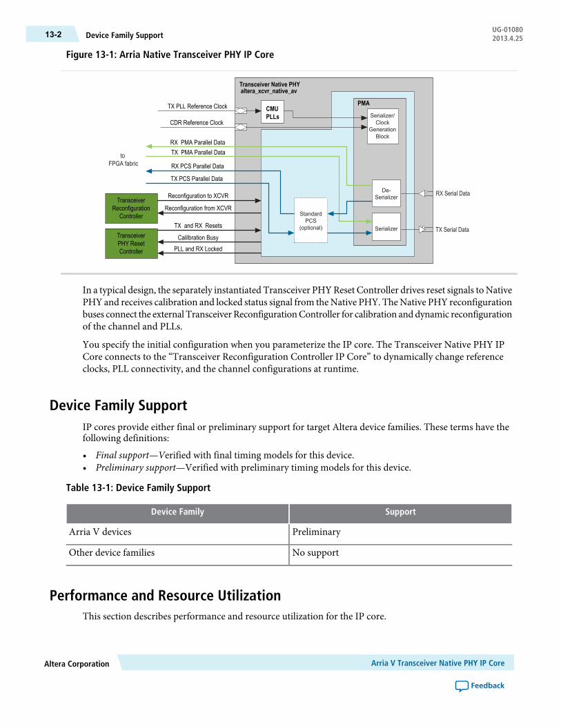
Figure 13-1: Arria Native Transceiver PHY IP Core
CMUPLLs
PMA
altera_xcvr_native_avTransceiver Native PHY
Reconfiguration to XCVR
Reconfiguration from XCVR
TX and RX Resets
Calilbration BusyPLL and RX Locked
RX PCS Parallel Data
TX PCS Parallel Data
CDR Reference Clock
TX PLL Reference Clock
RX Serial Data
toFPGA fabric
TX PMA Parallel DataRX PMA Parallel Data
TX Serial DataSerializer
De-Serializer
StandardPCS
(optional)
Serializer/Clock
GenerationBlock
TransceiverReconfiguration
Controller
TransceiverPHY ResetController
In a typical design, the separately instantiated Transceiver PHYReset Controller drives reset signals toNativePHY and receives calibration and locked status signal from theNative PHY. TheNative PHY reconfigurationbuses connect the external TransceiverReconfigurationController for calibration anddynamic reconfigurationof the channel and PLLs.
You specify the initial configuration when you parameterize the IP core. The Transceiver Native PHY IPCore connects to the “Transceiver Reconfiguration Controller IP Core” to dynamically change referenceclocks, PLL connectivity, and the channel configurations at runtime.
Device Family SupportIP cores provide either final or preliminary support for target Altera device families. These terms have thefollowing definitions:
• Final support—Verified with final timing models for this device.• Preliminary support—Verified with preliminary timing models for this device.
Table 13-1: Device Family Support
SupportDevice Family
PreliminaryArria V devices
No supportOther device families
Performance and Resource UtilizationThis section describes performance and resource utilization for the IP core.
Arria V Transceiver Native PHY IP CoreAltera Corporation
Feedback
UG-01080Device Family Support13-2 2013.4.25

Because the Standard PCS and PMAare implemented in hard logic, the Arria VNative PHY IPCore requiresminimal resources.
Parameterizing the Arria V Native PHYBy default, the Arria V Native PHY Transceiver PHY IP defaults to the PMA direct datapath and an internalPLL. You can change the default configuration to include the PCS or an external fractional PLL using theMegaWizard Plug-In Manager.
1. For Which device family will you be using?, select Arria V from the list.2. Click Installed Plug-Ins > Interfaces > Transceiver PHY > Arria V Native PHY v12.1 .3. Use the tabs on the MegaWizard Plug-In Manager to select the options required for the protocol.4. Click Finish to generate your customized Arria V Native PHY IP Core.
TheArria VTransceiverNative PHYprovides presets for CPRI, GIGE, and the LowLatency StandardPCS. The presets specify the parameters required to the protocol specified.
Note:
General ParametersThis section lists the parameters available on the General Options tab.
Table 13-2: General and Datapath Options
DescriptionRangeName
Specifies the speed grade.3fastest–6_H6Device speed grade
Allows you to specify the message level, as follows:
• error: Quartus II checker will not create an instance with invalidparameters. You must change incompatible parameter selectionsto proceed.
• warning: Quartus II checker will allow instance creation withinvalid parameters, but the instance will not compile successfully.
error warningMessage level for ruleviolations
Datapath Options
When you turn this option On, the core includes the TX datapath.On/OffEnable TX datapath
When you turn this option On, the core includes the RX datapath.On/OffEnable RX datapath
When you turn this option On, the core includes the Standard PCS.On/OffEnable StandardPCS
Specifies the total number of data channels in each direction.1-36Number of datachannels
Altera CorporationArria V Transceiver Native PHY IP Core
Feedback
13-3Parameterizing the Arria V Native PHYUG-010802013.4.25

DescriptionRangeName
In Non–bonded mode, each channel is assigned a PLL. DuringQuartus II compilation, the Fitter merges all PLLs that meet mergingrequirements into a single PLL.
Select×N to use the same clock source for up to 6 channels in a singletransceiver bank or the same clock source for all the transceivers onone side of the device. ×N bonding results in reduced clock skew.You must use contiguous channels when you select ×N bonding.
For more information about the clock architecture of bonding, referto “Transmitter Clock Network” in Transceiver Clocking in Arria VDevices in volume 2 of the Arria V Device Handbook.
Non–bonded
×N
Bonding mode
When you turn this option On, the data interface provides only therelevant interface to the FPGA fabric for the selected configuration.You can only use this option for static configurations.
When you turn this option Off, the data interface provides the fullphysical interface to the fabric. Select this option if you plan to usedynamic reconfiguration that includes changing the interface to theFPGA fabric.
Refer to “Active Bits for Each Fabric Interface Width” for guidance.
On/OffEnable simplifieddata interface
Related InformationTransceiver Clocking in Arria V Devices
PMA ParametersThis section describes the options available for the PMA.
For more information about the PMA, refer to the PMAArchitecture section in the Transceiver Architecturein Arria VDevices. Some parameters have ranges where the value is specified as Device Dependent. For suchparameters, the possible range of frequencies and bandwidths depends on the device, speed grade, and otherdesign characteristics. Refer to Device Datasheet for Arria V Devices for specific data for Arria V devices.
Table 13-3: PMA Options
DescriptionRangeParameter
Specifies the data rate. Themaximum data rate is 12.5 Gbps.
Device DependentData rate
Specifies the PMA to FPGA fabricinterface width for PMA Directmode.
8.10,16,20,64,80PMA direct interface width
Arria V Transceiver Native PHY IP CoreAltera Corporation
Feedback
UG-01080PMA Parameters13-4 2013.4.25

DescriptionRangeParameter
Specifies the value of the divideravailable in the transceiver channelsto divide the input clock to generatethe correct frequencies for theparallel and serial clocks. Thisdivisor divides the fast clock fromthe PLL in nonbondedconfigurations.
1, 2, 4, 8TX local clock division factor
Shows the base data rate of the clockinput to the TX PLL.The PLL basedata rate is computed from the TXlocal clock division factormultiplied by the data rate.
Select a PLL base data rate thatminimizes the number of PLLsrequired to generate all the clocksfor data transmission. By selectingan appropriate PLL base data rate,you can change data rates bychanging the TX local clockdivision factor used by the clockgeneration block.
Device DependentPLL base data rate
Related InformationTransceiver Architecture in Arria V Devices
Device Datasheet for Arria V Devices
TX PMA ParametersThis section describes the TX PMA options you can specify.
For more information about PLLs in Arria V devices, refer to the Arria V PLLs section in ClockNetworks and PLLs in Arria V Devices.
Note:
Table 13-4: TX PMA Parameters
DescriptionRangeParameter
When you turn this option On, you can dynamically reconfigurethe PLL. This option is also required to simulate TX PLLreconfiguration. If you turn this option On, the Quartus II Fitterprevents PLLmerging by default; however, you can specifymergingusing the FORCE_MERGE_PLL QSF assignments.
On/OffEnable TX PLLdynamicreconfiguration
Altera CorporationArria V Transceiver Native PHY IP Core
Feedback
13-5TX PMA ParametersUG-010802013.4.25
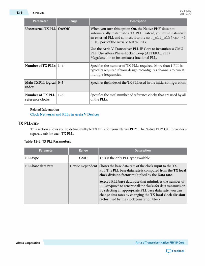
DescriptionRangeParameter
When you turn this option On, the Native PHY does notautomatically instantiate a TX PLL. Instead, you must instantiatean external PLL and connect it to the ext_pll_clk[<p> -1: 0] port of the Arria V Native PHY.
Use the Arria V Transceiver PLL IP Core to instantiate a CMUPLL. Use Altera Phase-Locked Loop (ALTERA_ PLL)Megafunction to instantiate a fractional PLL.
On/OffUse externalTXPLL
Specifies the number of TX PLLs required. More than 1 PLL istypically required if your design reconfigures channels to run atmultiple frequencies.
1–4Number ofTXPLLs
Specifies the index of the TX PLL used in the initial configuration.0–3MainTXPLL logicalindex
Specifies the total number of reference clocks that are used by allof the PLLs.
1–5Number of TX PLLreference clocks
Related InformationClock Networks and PLLs in Arria V Devices
TX PLL<n>This section allows you to define multiple TX PLLs for your Native PHY. The Native PHY GUI provides aseparate tab for each TX PLL.
Table 13-5: TX PLL Parameters
DescriptionRangeParameter
This is the only PLL type available.CMUPLL type
Shows the base data rate of the clock input to the TXPLL.The PLL base data rate is computed from the TX localclock division factor multiplied by the Data rate.
Select a PLL base data rate that minimizes the number ofPLLs required to generate all the clocks for data transmission.By selecting an appropriate PLL base data rate, you canchange data rates by changing the TX local clock divisionfactor used by the clock generation block.
Device DependentPLL base data rate
Arria V Transceiver Native PHY IP CoreAltera Corporation
Feedback
UG-01080TX PLL<n>13-6 2013.4.25

DescriptionRangeParameter
Specifies the frequency of the reference clock for the Selectedreference clock source index you specify. You can define asingle frequency for each PLL. You can use the TransceiverReconfiguration Controller to dynamically change thereference clock input to the PLL.
Note that the list of frequencies updates dynamically whenyou change the Data rate. The Input clock frequency dropdown menu is populated with all valid frequencies derivedas a function of the Data rate and Base data rate.
Device DependentReference clock frequency
You can define up to 5 reference clock sources for the PLLsin your core. The Reference clock frequency selected forindex 0, is assigned to TX PLL<0>. The Reference clockfrequency selected for index 1, is assigned to TX PLL<1>,and so on.
0–4Selected reference clocksource
Specifies nonbonded (separate) or shared PLLs for the clocknetwork.
non bonded ×NSelected clock network
RX PMA ParametersFor more information about the CDR circuitry, refer to the Receiver PMA Datapath section in theTransceiver Architecture in Arria V Devices .
Note:
Table 13-6: RX PMA Parameters
DescriptionRangeParameter
When you turn this option On, you can dynamically change thedata rate of the CDR circuit.
On/OffEnable CDRdynamicreconfiguration
Specifies the number of reference clocks for the CDRs.1–5Number of CDRreference clocks
Specifies the index of the selected CDR reference clock.0–4Selected CDRreference clock
Specifies the frequency of the clock input to the CDR.Device DependentSelected CDRreference clockfrequency
Specifies the maximum PPM difference the CDR can toleratebetween the input reference clock and the recovered clock.
Device DependentPPM detectorthreshold
When you turn this option On, the RX parallel clock which isrecovered from the serial received data is an output of the PMA.
On/OffEnablerx_pma_clkout port
Altera CorporationArria V Transceiver Native PHY IP Core
Feedback
13-7RX PMA ParametersUG-010802013.4.25
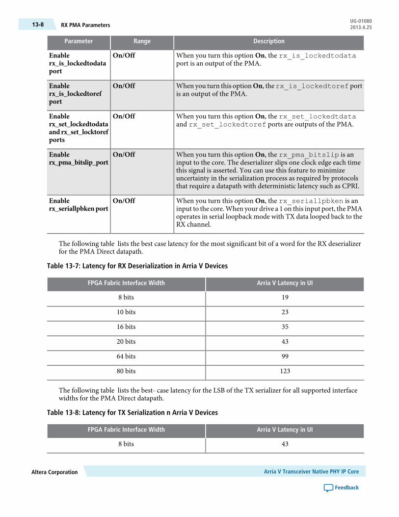
DescriptionRangeParameter
When you turn this option On, the rx_is_lockedtodataport is an output of the PMA.
On/OffEnablerx_is_lockedtodataport
When you turn this optionOn, therx_is_lockedtoref portis an output of the PMA.
On/OffEnablerx_is_lockedtorefport
When you turn this option On, the rx_set_lockedtdataand rx_set_lockedtoref ports are outputs of the PMA.
On/OffEnablerx_set_lockedtodataandrx_set_locktorefports
When you turn this option On, the rx_pma_bitslip is aninput to the core. The deserializer slips one clock edge each timethis signal is asserted. You can use this feature to minimizeuncertainty in the serialization process as required by protocolsthat require a datapath with deterministic latency such as CPRI.
On/OffEnablerx_pma_bitslip_port
When you turn this option On, the rx_seriallpbken is aninput to the core.When your drive a 1 on this input port, the PMAoperates in serial loopback mode with TX data looped back to theRX channel.
On/OffEnablerx_seriallpbkenport
The following table lists the best case latency for the most significant bit of a word for the RX deserializerfor the PMA Direct datapath.
Table 13-7: Latency for RX Deserialization in Arria V Devices
Arria V Latency in UIFPGA Fabric Interface Width
198 bits
2310 bits
3516 bits
4320 bits
9964 bits
12380 bits
The following table lists the best- case latency for the LSB of the TX serializer for all supported interfacewidths for the PMA Direct datapath.
Table 13-8: Latency for TX Serialization n Arria V Devices
Arria V Latency in UIFPGA Fabric Interface Width
438 bits
Arria V Transceiver Native PHY IP CoreAltera Corporation
Feedback
UG-01080RX PMA Parameters13-8 2013.4.25

Arria V Latency in UIFPGA Fabric Interface Width
5310 bits
6716 bits
8320 bits
13164 bits
16380 bits
The following table shows the bits used for all FPGA fabric to PMA interface widths. Regardless of the FPGAFabric Interface Width selected, all 80 bits are exposed for the TX and RX parallel data ports. However,depending upon the interface width selected not all bits on the bus will be active. The following table showswhich bits are active for each FPGA Fabric Interface Width selection. For example, if your interface is 16bits, the active bits on the bus are [17:0] and [7:0] of the 80 bit bus. The non-active bits are tied to ground.
Table 13-9: Active Bits for Each Fabric Interface Width
Bus Bits UsedFPGA Fabric Interface Width
[7:0]8 bits
[9:0]10 bits
{[17:10], [7:0]}16 bits
[19:0]20 bits
[39:0]40 bits
{[77:70], [67:60], [57:50], [47:40], [37:30], [27:20],[17:10], [7:0]}
64 bits
[79:0]80 bits
Related InformationTransceiver Architecture in Arria V Devices
Standard PCS ParametersThis section describes the standard PCS parameters.
The following figure shows the complete datapath and clocking for the Standard PCS. You use parametersavailable in the GUI to enable or disable the individual blocks in the Standard PCS.
Altera CorporationArria V Transceiver Native PHY IP Core
Feedback
13-9Standard PCS ParametersUG-010802013.4.25

Figure 13-2: The Standard PCS Datapath
Transmitter PCSTransmitter PMA
Receiver PMA Receiver PCS
FPGA Fabric
ByteOrdering
RXPh
ase
Comp
ensation
FIFO
ByteDe
serializer
8B/10
BDe
coder
RateMa
tchFIFO
WordA
ligner
Deserializer
CDR
TXPh
ase
Comp
ensation
FIFO
ByteSe
rializer
8B/10
BEn
coder
TXBitS
lip
Serializer
rx_serial_d
atatx_
serial_d
ata
tx_parallel data
rx_parallel data
/2
/2
tx_std_coreclkin
rx_std_coreclkin
Parallel Clock
SerialClock
Serial ClockParallel Clock
tx_std_clkout
rx_std_clkout
Formore information about the Standard PCS, refer to thePCSArchitecture section in theTransceiverArchitecture in Arria V Devices.
Note:
The following table describes the general and datapath options for the Standard PCS.
Table 13-10: General and Datapath Parameters
DescriptionRangeParameter
Specifies the protocol that you intend to implementwith theNativePHY. The protocol mode selected guides the MegaWizard inidentifying legal settings for the Standard PCS datapath.
Use the following guidelines to select a protocol mode:
• basic–select this mode for when none of the other options areappropriate. You should also select this mode to enablediagnostics, such as loopback.
• cpri–select this mode if you intend to implement CPRI oranother protocol that requires deterministic latency. Alterarecommends that you select the appropriate CPRI preset forthe CPRI protocol.
• gige–select this mode if you intend to implement either the1.25 Gbps or 2.5 Gbps Ethernet protocol. Altera recommendsthat you select the appropriate preset for the Ethernet protocol.
basic cpri gigeStandard PCSprotocol mode
Arria V Transceiver Native PHY IP CoreAltera Corporation
Feedback
UG-01080Standard PCS Parameters13-10 2013.4.25

DescriptionRangeParameter
Specifies the width of the datapath that connects the FPGA fabricto the PMA.The transceiver interfacewidth depends uponwhetheryou enable 8B/10B. To simplify connectivity between the FPGAfabric and PMA, the bus bits used are not contiguous for 16 and32bit buses. Refer to Active Bits for Each Fabric Interface Widthfor the bits used.
8, 10,16, 20StandardPCS/PMAinterface width
Shows the FPGA fabric to TX PCS interface width which iscalculated from the Standard PCS/PMA interface width .
8, 10,16, 20, 32, 40FPGAfabric/Standard TXPCS interface width
Shows the FPGA fabric to RX PCS interface width which iscalculated from the Standard PCS/PMA interface width .
8, 10,16, 20, 32, 40FPGAfabric/Standard RXPCS interface width
When you turn this option On, all PCS functions are disabledexcept for the phase compensation FIFO, byte serializer and bytedeserializer. This option creates the lowest latency Native PHYthat allows dynamic reconfigure between multiple PCS datapaths.
On/OffEnable ‘StandardPCS’ low latencymode
Phase Compensation FIFOThe phase compensation FIFO assures clean data transfer to and from the FPGA fabric by compensatingfor the clock phase difference between the lowspeed parallel clock and FPGA fabric interface clock.
For more information refer to the Receiver Phase Compensation FIFO and Transmitter PhaseCompensation FIFO sections in the Transceiver Architecture in Arria V Devices.
Note:
Table 13-11: Phase Compensation FIFO Parameters
DescriptionRangeParameter
The following 2 modes are possible:
• low_latency: This mode adds 3–4 cycles of latency to the TXdatapath.
• register_fifo: In this mode the FIFO is replaced by registers toreduce the latency through the PCS.Use thismode for protocolsthat require deterministic latency, such as CPRI.
low_latencyregister_fifo
TX FIFO mode
The following 2 modes are possible:
• low_latency: This mode adds 2–3 cycles of latency to the TXdatapath.
• register_fifo: In this mode the FIFO is replaced by registers toreduce the latency through the PCS.Use thismode for protocolsthat require deterministic latency, such as CPRI.
low_latencyregister_fifo
RX FIFO mode
Altera CorporationArria V Transceiver Native PHY IP Core
Feedback
13-11Phase Compensation FIFOUG-010802013.4.25

DescriptionRangeParameter
When you turn this optionOn, the TX Phase compensation FIFOoutputs a FIFO full status flag.
On/OffEnabletx_std_pcfifo_fullport
When you turn this optionOn, the TX Phase compensation FIFOoutputs a FIFO empty status flag.
On/OffEnabletx_std_pcfifo_emptyport
When you turn this optionOn, the RX Phase compensation FIFOoutputs a FIFO full status flag.
On/OffEnablerx_std_pcfifo_fullport
When you turn this optionOn, the RX Phase compensation FIFOoutputs a FIFO empty status flag.
On/OffEnablerx_std_pcfifo_emptyport
When you turn this option On, the rate match FIFO outputs aFIFO empty status flag. The rate match FIFO compensates forsmall clock frequency differences between the upstream transmitterand the local receiver clocks by inserting or removing skip (SKP)symbols or ordered sets from the interpacket gap (IPG) or idlestream.
On/OffEnablerx_std_rmfifo_emptyport
When you turn this option On, the rate match FIFO outputs aFIFO full status flag.
On/OffEnablerx_std_rmfifo_fullport
Related InformationTransceiver Architecture in Arria V Devices
Byte Ordering Block ParametersThis section describes the byte ordering block parameters.
The RXbyte ordering block realigns the data coming from the byte deserializer. This block is necessarywhenthe PCS to FPGA fabric interface width is greater than the PCS datapath. Because the timing of the RX PCSreset logic is indeterminate, the byte ordering at the output of the byte deserializer may or may not matchthe original byte ordering of the transmitted data.
For more information refer to the Byte Ordering section in the Transceiver Architecture in Arria VDevices.
Note:
Table 13-12: Byte Ordering Block Parameters
DescriptionRangeParameter
When you turn this option On, the PCS includes the byteordering block.
On/OffEnableRXbyteordering
Arria V Transceiver Native PHY IP CoreAltera Corporation
Feedback
UG-01080Byte Ordering Block Parameters13-12 2013.4.25
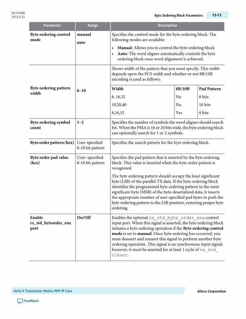
DescriptionRangeParameter
Specifies the control mode for the byte ordering block. Thefollowing modes are available:
• Manual: Allows you to control the byte ordering block• Auto: The word aligner automatically controls the byte
ordering block once word alignment is achieved.
manual
auto
Byte ordering controlmode
Shows width of the pattern that you must specify. This widthdepends upon the PCS width and whether or not 8B/10Bencoding is used as follows:
8–10Byte ordering patternwidth
Pad Pattern
8 bits
10 bits
9 bits
8B/10B
No
No
Yes
Width
8, 16,32
10,20,40
8,16,32
Specifies the number of symbols the word aligner should searchfor. When the PMA is 16 or 20 bits wide, the byte ordering blockcan optionally search for 1 or 2 symbols.
1–2Byte ordering symbolcount
Specifies the search pattern for the byte ordering block.User-specified8-10 bit pattern
Byte order pattern (hex)
Specifies the pad pattern that is inserted by the byte orderingblock. This value is inserted when the byte order pattern isrecognized.
The byte ordering pattern should occupy the least significantbyte (LSB) of the parallel TX data. If the byte ordering blockidentifies the programmed byte ordering pattern in the mostsignificant byte (MSB) of the byte-deserialized data, it insertsthe appropriate number of user-specified pad bytes to push thebyte ordering pattern to the LSB position, restoring proper byteordering.
User–specified8-10 bit pattern
Byte order pad value(hex)
Enables the optional rx_std_byte_order_ena controlinput port. When this signal is asserted, the byte ordering blockinitiates a byte ordering operation if the Byte ordering controlmode is set to manual. Once byte ordering has occurred, youmust deassert and reassert this signal to perform another byteordering operation. This signal is an synchronous input signal;however, it must be asserted for at least 1 cycle of rx_std_clkout.
On/OffEnablerx_std_byteorder_enaport
Altera CorporationArria V Transceiver Native PHY IP Core
Feedback
13-13Byte Ordering Block ParametersUG-010802013.4.25
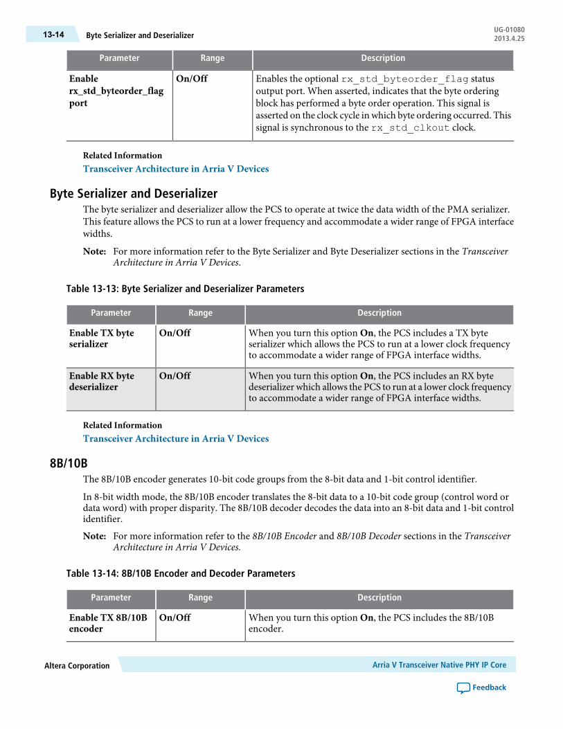
DescriptionRangeParameter
Enables the optional rx_std_byteorder_flag statusoutput port. When asserted, indicates that the byte orderingblock has performed a byte order operation. This signal isasserted on the clock cycle in which byte ordering occurred. Thissignal is synchronous to the rx_std_clkout clock.
On/OffEnablerx_std_byteorder_flagport
Related InformationTransceiver Architecture in Arria V Devices
Byte Serializer and DeserializerThe byte serializer and deserializer allow the PCS to operate at twice the data width of the PMA serializer.This feature allows the PCS to run at a lower frequency and accommodate a wider range of FPGA interfacewidths.
For more information refer to the Byte Serializer and Byte Deserializer sections in the TransceiverArchitecture in Arria V Devices.
Note:
Table 13-13: Byte Serializer and Deserializer Parameters
DescriptionRangeParameter
When you turn this option On, the PCS includes a TX byteserializer which allows the PCS to run at a lower clock frequencyto accommodate a wider range of FPGA interface widths.
On/OffEnable TX byteserializer
When you turn this option On, the PCS includes an RX bytedeserializer which allows the PCS to run at a lower clock frequencyto accommodate a wider range of FPGA interface widths.
On/OffEnable RX bytedeserializer
Related InformationTransceiver Architecture in Arria V Devices
8B/10BThe 8B/10B encoder generates 10-bit code groups from the 8-bit data and 1-bit control identifier.
In 8-bit width mode, the 8B/10B encoder translates the 8-bit data to a 10-bit code group (control word ordata word) with proper disparity. The 8B/10B decoder decodes the data into an 8-bit data and 1-bit controlidentifier.
For more information refer to the 8B/10B Encoder and 8B/10B Decoder sections in the TransceiverArchitecture in Arria V Devices.
Note:
Table 13-14: 8B/10B Encoder and Decoder Parameters
DescriptionRangeParameter
When you turn this option On, the PCS includes the 8B/10Bencoder.
On/OffEnable TX 8B/10Bencoder
Arria V Transceiver Native PHY IP CoreAltera Corporation
Feedback
UG-01080Byte Serializer and Deserializer13-14 2013.4.25

DescriptionRangeParameter
When you turn this optionOn, the PCS includes disparity controlfor the 8B/10B encoder. You force the disparity of the 8B/10Bencoder using the tx_forcedisp and tx_dispval controlsignal.
On/OffEnable TX 8B/10Bdisparity control
When you turn this option On, the PCS includes the 8B/10Bdecoder.
On/OffEnable RX 8B/10Bdecoder
Related InformationTransceiver Architecture in Arria V Devices
Rate Match FIFOThe rate match FIFO compensates for the very small frequency differences between the local system clockand the RX recovered clock.
For more information refer to the Rate Match FIFO sections in the Transceiver Architecture in Arria VDevices.
Table 13-15: Rate Match FIFO Parameters
DescriptionRangeParameter
When you turn this option On, the PCS includes a FIFO tocompensate for the very small frequency differences between thelocal system clock and the RX recovered clock.
On/OffEnable RX ratematch FIFO
Specifies the +ve (positive) disparity value for the RX rate matchFIFO as a hexadecimal string.
User-specified 20 bitpattern
RX rate matchinsert/delete +vepattern (hex)
Specifies the -ve (negative) disparity value for the RX rate matchFIFO as a hexadecimal string.
User-specified 20 bitpattern
RX rate matchinsert/delete -vepattern (hex)
Related InformationTransceiver Architecture in Arria V Devices
Word Aligner and BitSlip ParametersThe word aligner aligns the data coming from RX PMA deserializer to a given word boundary. When theword aligner operates in bitslip mode, the word aligner slips a single bit for every rising edge of the bit slipcontrol signal.
For more information refer to the Word Aligner section in the Transceiver Architecture in Arria VDevices.
Note:
Altera CorporationArria V Transceiver Native PHY IP Core
Feedback
13-15Rate Match FIFOUG-010802013.4.25
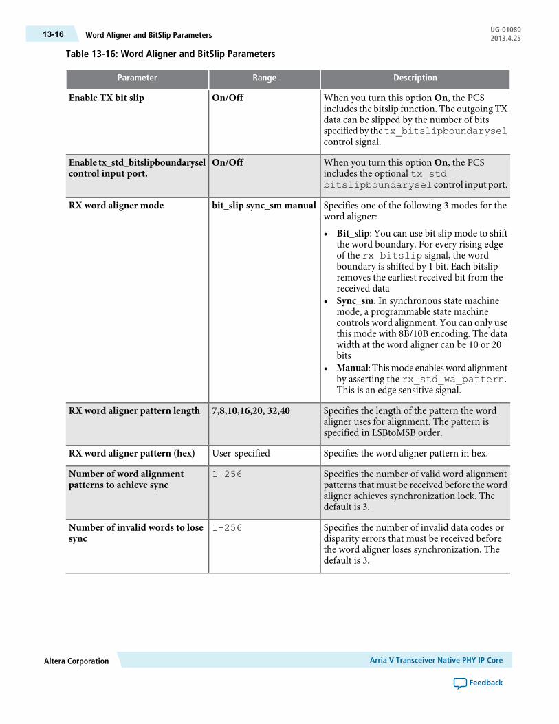
Table 13-16: Word Aligner and BitSlip Parameters
DescriptionRangeParameter
When you turn this option On, the PCSincludes the bitslip function. The outgoing TXdata can be slipped by the number of bitsspecifiedby thetx_bitslipboundaryselcontrol signal.
On/OffEnable TX bit slip
When you turn this option On, the PCSincludes the optional tx_std_bitslipboundarysel control input port.
On/OffEnable tx_std_bitslipboundaryselcontrol input port.
Specifies one of the following 3 modes for theword aligner:
• Bit_slip: You can use bit slip mode to shiftthe word boundary. For every rising edgeof the rx_bitslip signal, the wordboundary is shifted by 1 bit. Each bitslipremoves the earliest received bit from thereceived data
• Sync_sm: In synchronous state machinemode, a programmable state machinecontrols word alignment. You can only usethis mode with 8B/10B encoding. The datawidth at the word aligner can be 10 or 20bits
• Manual: Thismode enablesword alignmentby asserting the rx_std_wa_pattern.This is an edge sensitive signal.
bit_slip sync_sm manualRX word aligner mode
Specifies the length of the pattern the wordaligner uses for alignment. The pattern isspecified in LSBtoMSB order.
7,8,10,16,20, 32,40RX word aligner pattern length
Specifies the word aligner pattern in hex.User-specifiedRX word aligner pattern (hex)
Specifies the number of valid word alignmentpatterns that must be received before the wordaligner achieves synchronization lock. Thedefault is 3.
1–256Number of word alignmentpatterns to achieve sync
Specifies the number of invalid data codes ordisparity errors that must be received beforethe word aligner loses synchronization. Thedefault is 3.
1–256Number of invalid words to losesync
Arria V Transceiver Native PHY IP CoreAltera Corporation
Feedback
UG-01080Word Aligner and BitSlip Parameters13-16 2013.4.25
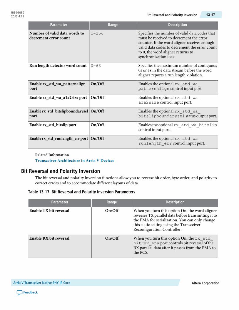
DescriptionRangeParameter
Specifies the number of valid data codes thatmust be received to decrement the errorcounter. If the word aligner receives enoughvalid data codes to decrement the error countto 0, the word aligner returns tosynchronization lock.
1–256Number of valid data words todecrement error count
Specifies the maximum number of contiguous0s or 1s in the data stream before the wordaligner reports a run length violation.
0–63Run length detector word count
Enables the optional rx_std_wa_patternalign control input port.
On/OffEnable rx_std_wa_patternalignport
Enables the optional rx_std_wa_a1a2size control input port.
On/OffEnable rx_std_wa_a1a2size port
Enables the optional rx_std_wa_bitslipboundarysel status output port.
On/OffEnable rx_std_bitslipboundaryselport
Enables the optionalrx_std_wa_bitslipcontrol input port.
On/OffEnable rx_std_bitslip port
Enables the optional rx_std_wa_runlength_err control input port.
On/OffEnable rx_std_runlength_errport
Related InformationTransceiver Architecture in Arria V Devices
Bit Reversal and Polarity InversionThe bit reversal and polarity inversion functions allow you to reverse bit order, byte order, and polarity tocorrect errors and to accommodate different layouts of data.
Table 13-17: Bit Reversal and Polarity Inversion Parameters
DescriptionRangeParameter
When you turn this option On, the word alignerreverses TX parallel data before transmitting it tothe PMA for serialization. You can only changethis static setting using the TransceiverReconfiguration Controller.
On/OffEnable TX bit reversal
When you turn this option On, the rx_std_bitrev_ena port controls bit reversal of theRX parallel data after it passes from the PMA tothe PCS.
On/OffEnable RX bit reversal
Altera CorporationArria V Transceiver Native PHY IP Core
Feedback
13-17Bit Reversal and Polarity InversionUG-010802013.4.25
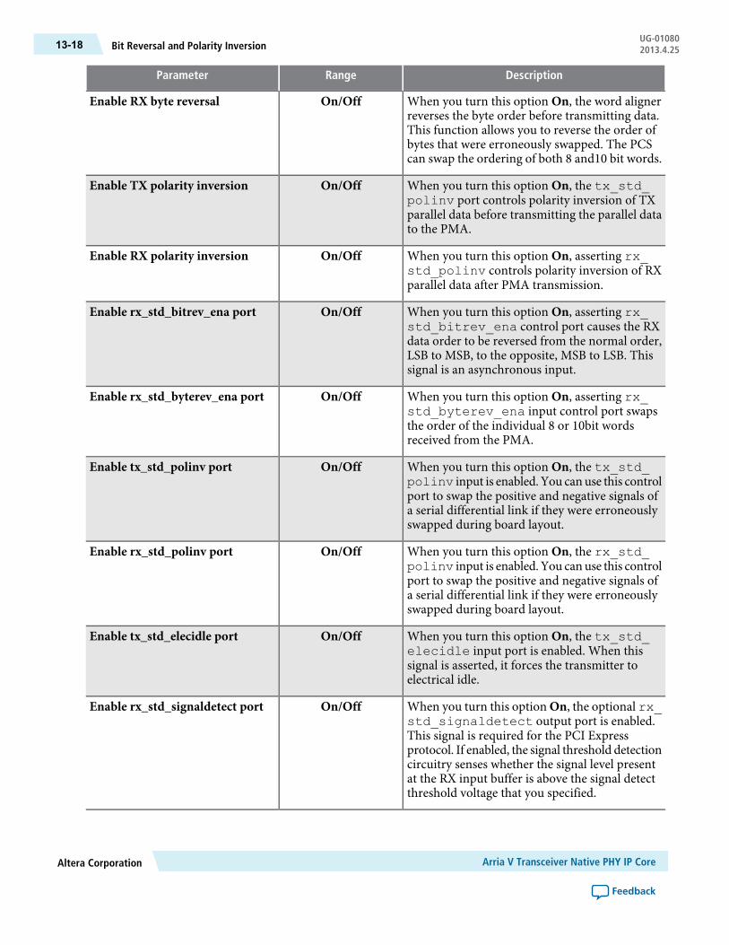
DescriptionRangeParameter
When you turn this option On, the word alignerreverses the byte order before transmitting data.This function allows you to reverse the order ofbytes that were erroneously swapped. The PCScan swap the ordering of both 8 and10 bit words.
On/OffEnable RX byte reversal
When you turn this option On, the tx_std_polinv port controls polarity inversion of TXparallel data before transmitting the parallel datato the PMA.
On/OffEnable TX polarity inversion
When you turn this option On, asserting rx_std_polinv controls polarity inversion of RXparallel data after PMA transmission.
On/OffEnable RX polarity inversion
When you turn this option On, asserting rx_std_bitrev_ena control port causes the RXdata order to be reversed from the normal order,LSB to MSB, to the opposite, MSB to LSB. Thissignal is an asynchronous input.
On/OffEnable rx_std_bitrev_ena port
When you turn this option On, asserting rx_std_byterev_ena input control port swapsthe order of the individual 8 or 10bit wordsreceived from the PMA.
On/OffEnable rx_std_byterev_ena port
When you turn this option On, the tx_std_polinv input is enabled. You canuse this controlport to swap the positive and negative signals ofa serial differential link if they were erroneouslyswapped during board layout.
On/OffEnable tx_std_polinv port
When you turn this option On, the rx_std_polinv input is enabled. You canuse this controlport to swap the positive and negative signals ofa serial differential link if they were erroneouslyswapped during board layout.
On/OffEnable rx_std_polinv port
When you turn this option On, the tx_std_elecidle input port is enabled. When thissignal is asserted, it forces the transmitter toelectrical idle.
On/OffEnable tx_std_elecidle port
When you turn this option On, the optional rx_std_signaldetect output port is enabled.This signal is required for the PCI Expressprotocol. If enabled, the signal threshold detectioncircuitry senses whether the signal level presentat the RX input buffer is above the signal detectthreshold voltage that you specified.
On/OffEnable rx_std_signaldetect port
Arria V Transceiver Native PHY IP CoreAltera Corporation
Feedback
UG-01080Bit Reversal and Polarity Inversion13-18 2013.4.25
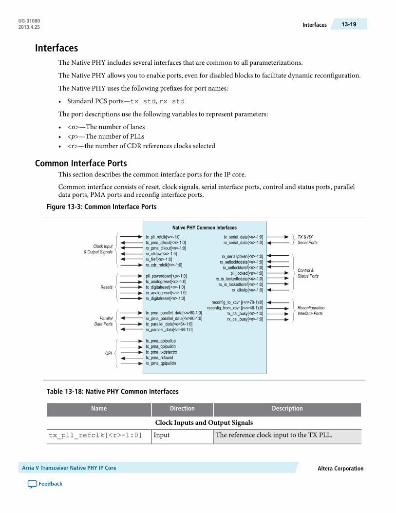
InterfacesThe Native PHY includes several interfaces that are common to all parameterizations.
The Native PHY allows you to enable ports, even for disabled blocks to facilitate dynamic reconfiguration.
The Native PHY uses the following prefixes for port names:
• Standard PCS ports—tx_std, rx_std
The port descriptions use the following variables to represent parameters:
• <n>—The number of lanes• <p>—The number of PLLs• <r>—the number of CDR references clocks selected
Common Interface PortsThis section describes the common interface ports for the IP core.
Common interface consists of reset, clock signals, serial interface ports, control and status ports, paralleldata ports, PMA ports and reconfig interface ports.
Figure 13-3: Common Interface Ports
tx_pll_refclk[<r>-1:0]tx_pma_clkout[<n>-1:0]rx_pma_clkout[<n>-1:0]rx_clklow[<n>-1:0]rx_fref[<n>-1:0]rx_cdr_refclk[<r>-1:0]
Clock Input& Output Signals
rx_seriallpbken[<n>-1:0]rx_setlocktodata[<n>-1:0]rx_setlocktoref[<n>-1:0]
pll_locked[<p>-1:0]rx_is_lockedtodata[<n>-1:0]rx_is_lockedtoref[<n>-1:0]
rx_clkslip[<n>-1:0]
Control &Status Portspll_powerdown[<p>-1:0]
tx_analogreset[<n>-1:0]tx_digitalreset[<n>-1:0]rx_analogreset[<n>-1:0]rx_digitalreset[<n>-1:0]
Resets
QPI
tx_pma_parallel_data[<n>80-1:0]rx_pma_parallel_data[<n>80-1:0]tx_parallel_data[<n>64-1:0]rx_parallel_data[<n>64-1:0]
tx_pma_qpipulluptx_pma_qpipulldntx_pma_txdetectrxtx_pma_rxfoundrx_pma_qpipulldn
ParallelData Ports
tx_serial_data[<n>-1:0]rx_serial_data[<n>-1:0]
TX & RXSerial Ports
reconfig_to_xcvr [(<n>70-1):0]reconfig_from_xcvr [(<n>46-1):0]
tx_cal_busy[<n>-1:0]rx_cal_busy[<n>-1:0]
ReconfigurationInterface Ports
Native PHY Common Interfaces
Table 13-18: Native PHY Common Interfaces
DescriptionDirectionName
Clock Inputs and Output Signals
The reference clock input to the TX PLL.Inputtx_pll_refclk[<r>-1:0]
Altera CorporationArria V Transceiver Native PHY IP Core
Feedback
13-19InterfacesUG-010802013.4.25
DescriptionDirectionName
TX parallel clock output from PMA. This clock isonly available in PMA direct mode.
Outputtx_pma_clkout[<n>-1:0]
RX parallel clock (recovered clock) output fromPMA
Outputrx_pma_clkout[<n>-1:0]
The RX parallel recovered clock input to the phasefrequency detector (PFD).When operatingCDR inmanual lock mode, you can use this clock as aninput with rx_fref to an external PPM detector.
Outputrx_clklow[<n>-1:0]
TheRX local reference lock input to the PFD.Whenoperating CDR in manual lock mode, you can usethis clock with rx_clklow as an input to anexternal PPM detector.
Outputrx_fref[<n>-1:0]
Input reference clock for the RX PFD circuit.Inputrx_cdr_refclk[<n>-1:0]
Resets
When asserted, resets the TXPLL. Active high, edgesensitive reset signal. By default, the Arria V NativeTransceiver PHY IP Core creates a separate pll_powerdown signal for each logical PLL. However,the Fittermaymerge the PLLs if they are in the sametransceiver bank. PLLs can only be merged if theirpll_powerdown signals are driven from the samesource. If the PLLs are in separate transceiver banks,you can choose to drive the pll_powerdownsignals separately.
Inputpll_powerdown[<p>-1:0]
When asserted, resets for TX PMA, TX clockgeneration block, and serializer. Active high, edgesensitive reset signal.
Inputtx_analogreset[<n>-1:0]
When asserted, resets the digital components of theTX datapath. Active high, edge sensitive,asynchronous reset signal. If your design includesbonded TX PCS channels, refer to TimingConstraints for Reset Signals when Using BondedPCS Channels for a SDC constraint you mustinclude in your design.
Inputtx_digitalreset[<n>-1:0]
When asserted, resets the RX CDR, deserializer.Active high, edge sensitive, asynchronous resetsignal.
Inputrx_analogreset[<n>-1:0]
When asserted, resets the digital components of theRX datapath. Active high, edge sensitive,asynchronous reset signal.
Inputrx_digitalreset[<n>-1:0]
Parallel data ports
Arria V Transceiver Native PHY IP CoreAltera Corporation
Feedback
UG-01080Common Interface Ports13-20 2013.4.25

DescriptionDirectionName
TX parallel data for the PMA Direct datapath.Driven directly from the FPGA fabric to the PMA.Not used when you enable the Standard PCSdatapath.
Inputtx_pma_parallel_data[79:0]
RX PMA parallel data driven from the PMA to theFPGA fabric. Not used when you enable theStandard PCS datapath.
Outputrx_pma_parallel_data[79:0]
PCS TX parallel data. Used when you enable theStandard datapath.
Inputtx_parallel_data[43:0]
PCS RX parallel data. Used when you enable theStandard datapath.
Outputrx_parallel_data[63:0]
TX and RX serial ports
TX differential serial output data.Outputtx_serial_data[<n>-1:0]
RX differential serial output data.Inputrx_serial_data[<n>-1:0]
Control and Status ports
When asserted, the transceiver enters serial loopbackmode. Loopback drives serial TX data to the RXinterface.
Inputrx_seriallpbken[<n>-1:0]
When asserted, programs the RX CDR to manuallock to data mode in which you control the resetsequence using the rx_set_locktoref andrx_set_locktodata. Refer to “TransceiverReset Sequence” in Transceiver Reset Control inArriaVDevices formore information aboutmanualcontrol of the reset sequence.
Inputrx_set_locktodata[<n>-1:0]
When asserted, programs the RX CDR to manuallock to reference mode in which you control thereset sequence using the rx_set_locktorefand rx_set_locktodata. Refer to Refer to“Transceiver Reset Sequence” in Transceiver ResetControl in Arria V Devices for more informationabout manual control of the reset sequence.
Inputrx_set_locktoref[<n>-1:0]
When asserted, indicates that the PLL is locked tothe input reference clock.
Outputpll_locked[<p>-1:0]
When asserted, the CDR is locked to the incomingdata.
Outputrx_is_lockedtodata[<n>-1:0]
When asserted, the CDR is locked to the incomingreference clock.
Outputrx_is_lockedtoref[<n>-1:0]
When asserted, the deserializer slips one clock edge.Inputrx_clkslip[<n>-1:0]
Altera CorporationArria V Transceiver Native PHY IP Core
Feedback
13-21Common Interface PortsUG-010802013.4.25
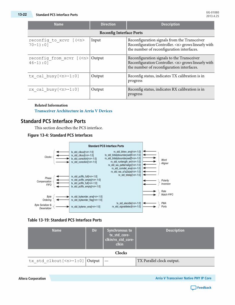
DescriptionDirectionName
Reconfig Interface Ports
Reconfiguration signals from the TransceiverReconfigurationController. <n> grows linearlywiththe number of reconfiguration interfaces.
Inputreconfig_to_xcvr [(<n>70-1):0]
Reconfiguration signals to the TransceiverReconfigurationController. <n> grows linearlywiththe number of reconfiguration interfaces.
Outputreconfig_from_xcvr [(<n>46-1):0]
Reconfig status, indicates TX calibration is inprogress
Outputtx_cal_busy[<n>-1:0]
Reconfig status, indicates RX calibration is inprogress
Outputrx_cal_busy[<n>-1:0]
Related InformationTransceiver Architecture in Arria V Devices
Standard PCS Interface PortsThis section describes the PCS interface.
Figure 13-4: Standard PCS Interfaces
ClocksWordAligner
PhaseCompensation
FIFO
ByteOrdering
rx_std_rmfifo_empty[<n>-1:0]rx_std_rmfifo_full[<n>-1:0]
RateMatch FIFO
rx_std_polinv[<n>-1:0]tx_std_polinv[<n>-1:0]
PolarityInversion
PMAPorts
Standard PCS Interface Portsrx_std_bitrev_ena[<n>-1:0]
tx_std_bitslipboundarysel[5<n>-1:0]rx_std_bitslipboundarysel[5<n>-1:0]
rx_std_runlength_err[<n>-1:0]rx_std_wa_patternalign[<n>-1:0]
rx_std_comdet_ena[<n>-1:0]rx_std_wa_a1a2size[<n>-1:0]
rx_std_bitslip[<n>-1:0]
tx_std_elecidle[<n>-1:0]rx_std_signaldetect[<n>-1:0]rx_std_byterev_ena[<n>-1:0]Byte Serializer &
Deserializer
tx_std_clkout[<n>-1:0]rx_std_clkout[<n>-1:0]tx_std_coreclkin[<n>-1:0]rx_std_coreclkin[<n>-1:0]
rx_std_pcfifo_full[<n>-1:0]rx_std_pcfifo_empty[<n>-1:0]tx_std_pcfifo_full[<n>-1:0]tx_std_pcfifo_empty[<n>-1:0]
rx_std_byteorder_ena[<n>-1:0]rx_std_byteorder_flag[<n>-1:0]
Table 13-19: Standard PCS Interface Ports
DescriptionSynchronous totx_std_core-
clkin/rx_std_core-clkin
DirName
Clocks
TX Parallel clock output.—Outputtx_std_clkout[<n>-1:0]
Arria V Transceiver Native PHY IP CoreAltera Corporation
Feedback
UG-01080Standard PCS Interface Ports13-22 2013.4.25

DescriptionSynchronous totx_std_core-
clkin/rx_std_core-clkin
DirName
RX parallel clock output. The CDR circuitryrecovers RX parallel clock from the RX datastream.
—Outputrx_std_clkout[<n>-1:0]
TX parallel clock input from the FPGA fabricthat drives the write side of the TX phasecompensation FIFO.
—Inputtx_std_coreclkin[<n>-1:0]
RX parallel clock that drives the read side ofthe RX phase compensation FIFO.
—Inputrx_std_coreclkin[<n>-1:0]
Phase Compensation FIFO
RX phase compensation FIFO full status flag.YesOutputrx_std_pcfifo_full[<n>-1:0]
RX phase compensation FIFO status emptyflag.
YesOutputrx_std_pcfifo_empty[<n>-1:0]
TX phase compensation FIFO status full flag.YesOutputtx_std_pcfifo_full[<n>-1:0]
TX phase compensation FIFO status emptyflag.
YesOutputtx_std_pcfifo_empty[<n>-1:0]
Byte Ordering
Byte ordering enable. When this signal isasserted, the byte ordering block initiates abyte ordering operation if the Byte orderingcontrol mode is set to manual. Once byteordering has occurred, you must deassert andreassert this signal to perform another byteordering operation. This signal is ansynchronous input signal; however, it must beasserted for at least 1 cycle of rx_std_clkout.
NoInputrx_std_byteorder_ena[<n>-1:0]
Byte ordering status flag. When asserted,indicates that the byte ordering block hasperformed a byte order operation. This signalis asserted on the clock cycle in which byteordering occurred. This signal is synchronousto the rx_std_clkout clock. You must asynchronizer this signal.
YesOutputrx_std_byteorder_flag[<n>-1:0]
Byte Serializer and Deserializer
Altera CorporationArria V Transceiver Native PHY IP Core
Feedback
13-23Standard PCS Interface PortsUG-010802013.4.25

DescriptionSynchronous totx_std_core-
clkin/rx_std_core-clkin
DirName
This control signal is available in when thePMA width is 16 or 20 bits. When asserted,enables byte reversal on the RX interface.
NoInputrx_std_byterev_ena[<n>-1:0]
8B/10B
Polarity inversion for the 8B/10B decoder,When set, the RX channels invert the polarityof the received data. You can use this signalto correct the polarity of differential pairs ifthe transmission circuitry or board layoutmistakenly swapped the positive and negativesignals. The polarity inversion functionoperates on the word aligner input.
NoInputrx_std_polinv[<n>-1:0]
Polarity inversion, part of 8B10B encoder,When set, the TX interface inverts the polarityof the TX data.
NoInputtx_std_polinv[<n>-1:0]
Rate Match FIFO
Rate match FIFO empty flag. When asserted,the rate match FIFO is empty.
NoOutputrx_std_rmfifo_empty[<n>-1:0]
Rate match FIFO full flag. When asserted theratematch FIFO is full. Youmust synchronizethis signal.
NoOutputrx_std_rmfifo_full[<n>-1:0]
Word Aligner
When asserted, enables bit reversal on the RXinterface. Bit order may be reversed if externaltransmission circuitry transmits the mostsignificant bit first.When enabled, the receivecircuitry receives all words in the reverseorder. The bit reversal circuitry operates onthe output of the word aligner.
NoInputrx_std_bitrev_ena[<n>-1:0]
BitSlip boundary selection signal. Specifies thenumber of bits that the TX bit slipper mustslip.
NoInputtx_std_bitslipboundarysel[5<n>-1:0]
This signal operates when the word aligner isin bitslip word alignment mode. It reports thenumber of bits that the RX block slipped toachieve deterministic latency.
NoOutputrx_std_bitslipboundarysel[5<n>-1:0]
Arria V Transceiver Native PHY IP CoreAltera Corporation
Feedback
UG-01080Standard PCS Interface Ports13-24 2013.4.25
DescriptionSynchronous totx_std_core-
clkin/rx_std_core-clkin
DirName
When asserted, indicates a run lengthviolation. Asserted if the number ofconsecutive 1s or 0s exceeds the numberspecified in the parameter editor GUI.
NoOutputrx_std_runlength_err[<n>-1:0]
Active when you place the word aligner inmanual mode. In manual mode, you alignwords by asserting rx_st_wa_patternalign.rx_st_wa_patternalign is edge sensitive.
For more information refer to the WordAligner section in theTransceiver Architecturein Arria V Devices.
NoInputrx_st_wa_patternalign
Used for the SONET protocol. Assert whentheA1 andA2 framing bytesmust be detected.A1 and A2 are SONET backplane bytes andare only used when the PMA data width is 8bits.
NoInputrx_std_wa_a1a2size[<n>-1:0]
Usedwhenword alignermode is bitslipmode.For every rising edge of the rx_std_bitslip signal, theword boundary is shiftedby 1 bit. Each bitslip removes the earliestreceived bit from the received data. You mustsynchronize this signal.
NoInputrx_std_bitslip[<n>-1:0]
Miscellaneous
When asserted, enables a circuit to detect adownstream receiver. This signal must bedriven low when not in use because it causesthe TXPMA to enter electrical idlemodewiththe TX serial data signals in tristate mode.
Inputtx_std_elecidle[<n>-1:0]
Signal threshold detect indicator. Whenasserted, it indicates that the signal present atthe receiver input buffer is above theprogrammed signal detection threshold value.You must synchronize this signal.
NoOutputrx_std_signaldetect[<n>-1:0]
Related InformationTransceiver Architecture in Stratix V Devices
Altera CorporationArria V Transceiver Native PHY IP Core
Feedback
13-25Standard PCS Interface PortsUG-010802013.4.25

SDC Timing ConstraintsThis section describes SDC timing constraints.
The Quartus II 12.1 software reports timing violations for asynchronous inputs to the Standard PCS and10G PCS. Because many violations are for asynchronous paths, they do not represent actual timing failures.You may choose one of the following three approaches to identify these false timing paths to the Quartus IIor TimeQuest software.
• You can cut these paths in your SynopsysDesignConstraints (.sdc) file by using theset_false_pathcommand as shown in the following example.
Example 13-1: Using the set_false_path Constraint to Identify Asynchronous Inputs
set_false_path -through {*8gbitslip*} -to [get_registers*8g_rx_pcs*SYNC_DATA_REG*]set_false_path -through {*8gbytordpld*} -to [get_registers*8g_rx_pcs*SYNC_DATA_REG*]set_false_path -through {*8gcmpfifoburst*} -to [get_registers*8g_rx_pcs*SYNC_DATA_REG*]set_false_path -through {*8gphfifoburstrx*} -to [get_registers*8g_rx_pcs*SYNC_DATA_REG*]
set_false_path -through {*8gsyncsmen*} -to [get_registers*8g*pcs*SYNC_DATA_REG*]set_false_path -through {*8gwrdisablerx*} -to [get_registers*8g_rx_pcs*SYNC_DATA_REG*]set_false_path -through {*rxpolarity*} -to [get_registers*SYNC_DATA_REG*]set_false_path -through {*pldeidleinfersel*} -to [get_registers*SYNC_DATA_REG*]
• You can use the set_max_delay constraint on a given path to create a constraint for asynchronoussignals that do not have a specific clock relationship but require a maximum path delay.
Example 13-2: Using the max_delay Constraint to Identify Asynchronous Inputs
# Example: Apply 10ns max delayset_max_delay -from *tx_from_fifo* -to *8g*pcs*SYNC_DATA_REG1 10
• You can use the set_false path command only during Timequest timing analysis.
Example 13-3: Using the set_false TimeQuest Constraint to Identify Asynchronous Inputs
#if {$::TimeQuestInfo(nameofexecutable) eq "quartus_fit"} {#} else {
Arria V Transceiver Native PHY IP CoreAltera Corporation
Feedback
UG-01080SDC Timing Constraints13-26 2013.4.25

#set_false_path -from [get_registers {*tx_from_fifo*}] -through{*txbursten*} -to [get_registers *8g_*_pcs*SYNC_DATA_REG
In in all of these examples, you must substitute you actual signal names for the signal names shown.Note:
Dynamic ReconfigurationDynamic reconfiguration calibrates each channel to compensate for variations due to process, voltage, andtemperature (PVT).
As silicon progresses towards smaller process nodes, circuit performance is affected more by variations dueto process, voltage, and temperature (PVT). These process variations result in analog voltages that can beoffset from required ranges. The calibration performed by the dynamic reconfiguration interface compensatesfor variations due to PVT.
For nonbonded clocks, each channel and each TX PLL has a separate dynamic reconfiguration interfaces.The MegaWizard Plug-In Manager provides informational messages on the connectivity of these interfaces.The following example shows the messages for the Arria V Native PHY with four duplex channels, four TXPLLs, in a nonbonded configuration.
For more information about transceiver reconfiguration refer to Transceiver Reconfiguration Controller IPCore.
Example 13-4: Informational Messages for the Transceiver Reconfiguration Interface
PHY IP will require 8 reconfiguration interfaces for connectionto the external reconfiguration controller.Reconfiguration interface offsets 0-3 are connected to thetransceiver channels.Reconfiguration interface offsets 4–7 are connected to thetransmit PLLs.
Related InformationTransceiver Architecture in Arria V Devices
Simulation SupportThe Quartus II 12.1 release provides simulation and compilation support for the Arria V Native PHY IPCore. Refer to Running a Simulation Testbench for a description of the directories and files that theQuartus IIsoftware creates automatically when you generate your Arria V Transceiver Native PHY IP Core.
Altera CorporationArria V Transceiver Native PHY IP Core
Feedback
13-27Dynamic ReconfigurationUG-010802013.4.25

14Arria V GZ Transceiver Native PHY IP Core
2013.4.25UG-01080 Subscribe Feedback
Unlike other PHY IP Cores, the Native PHY IP Core does not include an Avalon Memory-Mapped(Avalon-MM) interface. Instead, it exposes all signals directly as ports. The Arria V GZ Transceiver NativePHY IP Core provides the following three datapaths:
• Standard PCS• 10G PCS• PMA Direct
You can enable the Standard PCS, the 10G PCS, or both if your design uses the Transceiver ReconfigurationController to change dynamically between the two PCS datapaths. The transceiver PHY does not includean embedded reset controller. You can either design custom reset logic or incorporate Altera’s “TransceiverPHY Reset Controller IP Core” to implement reset functionality.
In PMADirectmode, theNative PHYprovides direct access to the PMA from the FPGA fabric; consequently,the latency for transmitted and received data is very low. However, you must implement any PCS functionthat your design requires in the FPGA fabric.
The following figure illustrates the use of the Arria V GZ Transceiver Native PHY IP Core. As this figureillustrates, TX PLL and clock data recovery (CDR) reference clocks from the pins of the device are input tothe PLLmodule andCDR logic.When enabled, the 10Gor Standard PCS drives TXparallel data and receivesRX parallel data. When neither PCS is enabled the Native PHY operates in PMA Direct mode.
ISO9001:2008Registered
© 2013 Altera Corporation. All rights reserved. ALTERA, ARRIA, CYCLONE, HARDCOPY, MAX, MEGACORE, NIOS, QUARTUS and STRATIXwords and logos are trademarks of Altera Corporation and registered in the U.S. Patent and Trademark Office and in other countries. All other wordsand logos identified as trademarks or service marks are the property of their respective holders as described at www.altera.com/common/legal.html.Altera warrants performance of its semiconductor products to current specifications in accordance with Altera's standard warranty, but reserves theright to make changes to any products and services at any time without notice. Altera assumes no responsibility or liability arising out of the applicationor use of any information, product, or service described herein except as expressly agreed to in writing by Altera. Altera customers are advised toobtain the latest version of device specifications before relying on any published information and before placing orders for products or services.
www.altera.com
101 Innovation Drive, San Jose, CA 95134
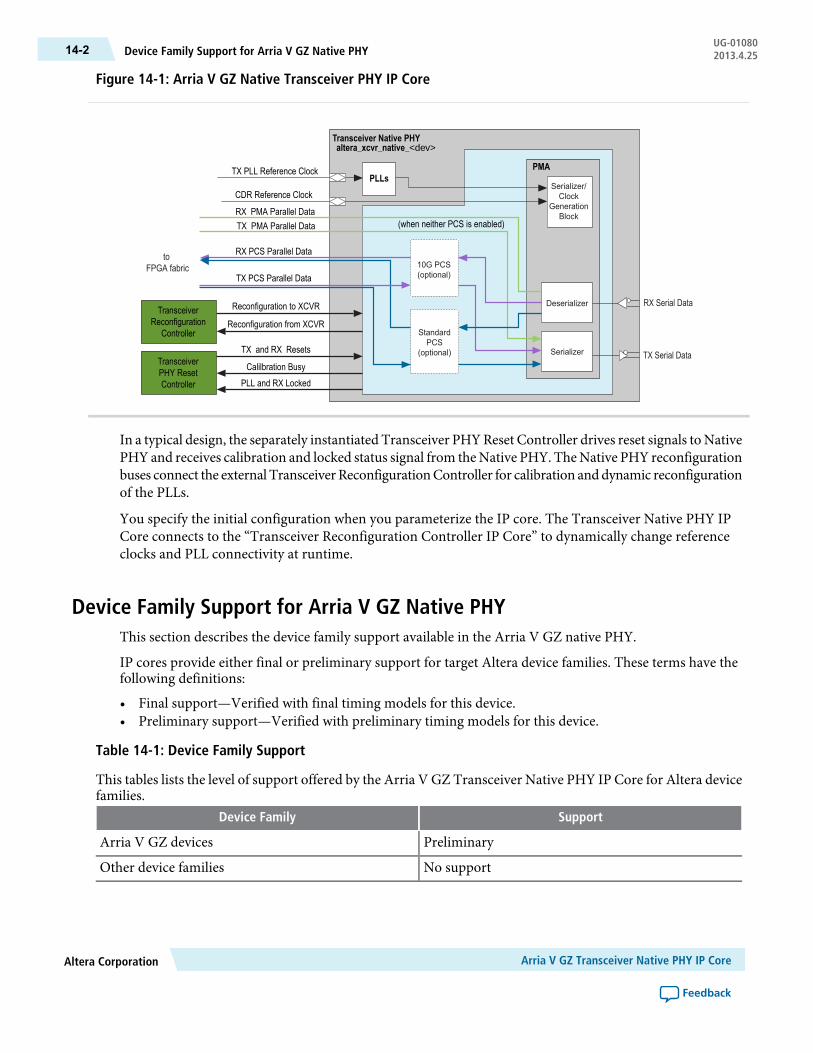
Figure 14-1: Arria V GZ Native Transceiver PHY IP Core
PLLsPMA
altera_xcvr_native_<dev>Transceiver Native PHY
TransceiverReconfiguration
Controller
Reconfiguration to XCVR
Reconfiguration from XCVR
TX and RX Resets
Calilbration BusyPLL and RX Locked
RX PCS Parallel Data
TX PCS Parallel Data
CDR Reference Clock
(when neither PCS is enabled)
TX PLL Reference ClockSerializer/Clock
GenerationBlock
RX Serial Data
toFPGA fabric
TransceiverPHY ResetController
TX PMA Parallel DataRX PMA Parallel Data
TX Serial DataSerializer
Deserializer
StandardPCS
(optional)
10G PCS(optional)
In a typical design, the separately instantiated Transceiver PHYReset Controller drives reset signals toNativePHY and receives calibration and locked status signal from theNative PHY. TheNative PHY reconfigurationbuses connect the external TransceiverReconfigurationController for calibration anddynamic reconfigurationof the PLLs.
You specify the initial configuration when you parameterize the IP core. The Transceiver Native PHY IPCore connects to the “Transceiver Reconfiguration Controller IP Core” to dynamically change referenceclocks and PLL connectivity at runtime.
Device Family Support for Arria V GZ Native PHYThis section describes the device family support available in the Arria V GZ native PHY.
IP cores provide either final or preliminary support for target Altera device families. These terms have thefollowing definitions:
• Final support—Verified with final timing models for this device.• Preliminary support—Verified with preliminary timing models for this device.
Table 14-1: Device Family Support
This tables lists the level of support offered by the Arria V GZ Transceiver Native PHY IP Core for Altera devicefamilies.
SupportDevice Family
PreliminaryArria V GZ devices
No supportOther device families
Arria V GZ Transceiver Native PHY IP CoreAltera Corporation
Feedback
UG-01080Device Family Support for Arria V GZ Native PHY14-2 2013.4.25

Performance and Resource Utilization for Arria V GZ Native PHYBecause the 10G PCS, Standard PCS, and PMA are implemented in hard logic, the Arria V GZ Native PHYIP Core uses less than 1% of the available ALMs, memory, primary and secondary logic registers.
Parameter PresetsPresets allow you to specify a group of parameters to implement a particular protocol or application.
If you apply a preset, the parameters with specific required values are set for you. When applied, the presetis in boldface and remains as such unless you change some of the preset parameters. Selecting a preset doesnot prevent you from changing any parameter tomeet the requirements of your design. The following figureillustrates the Preset panel and form to create custom presets.
Figure 14-2: Preset Panel and Form To Create Custom Presets
Parameterizing the Arria V GZ Native PHYThis section provides a list of instructions on how to configure the Arria V GZ native PHY IP core usingthe MegaWizard.
Complete the following steps to configure the Arria V GZ Native PHY IP Core in the MegaWizard Plug-InManager:
1. For Which device family will you be using? select Arria V GZ from the list.2. Click Installed Plug-Ins > Interfaces > Transceiver PHY > Arria V GZ Native PHY v12.1.3. Use the tabs on the MegaWizard Plug-In Manager to select the options required for the protocol.4. Click Finish.
Clicking Finish generates your customized Arria V GZ Native PHY IP Core.
Altera CorporationArria V GZ Transceiver Native PHY IP Core
Feedback
14-3Performance and Resource Utilization for Arria V GZ Native PHYUG-010802013.4.25

General Parameters for Arria V GZ Native PHYThis section describes the datapath parameters in the General Options tab for the Arria V GZ native PHY.
Table 14-2: General and Datapath Options
The following table lists the parameters available on the General Options tab. Note that you can enable theStandard PCS, the 10G PCS, or both if you intend to reconfigure between the two available PCS datapaths.
DescriptionRangeName
Specifies the speed grade.fastest - 3_H3Device speed grade
When you select the error message level, theQuartus II rules checker reports an error if youspecify incompatible parameters. If you select thewarningmessage level, theQuartus II rules checkerreports a warning instead of an error.
error
warning
Message level for ruleviolations
Datapath Options
When you turn this option On, the core includesthe TX datapath.
On/OffEnable TX datapath
When you turn this option On, the core includesthe RX datapath.
On/OffEnable RX datapath
When you turn this option On, the core includesthe Standard PCS . You can enable both theStandard and 10G PCS if you plan to dynamicallyreconfigure the Native PHY.
On/OffEnable Standard PCS
When you turn this option On, the core includesthe 10G PCS. You can enable both the Standardand 10G PCS if you plan to dynamicallyreconfigure the Native PHY.
On/OffEnable 10G PCS
Specifies the total number of data channels in eachdirection. From 1-32 channels are supported.
Device DependentNumber of data channels
Arria V GZ Transceiver Native PHY IP CoreAltera Corporation
Feedback
UG-01080General Parameters for Arria V GZ Native PHY14-4 2013.4.25
DescriptionRangeName
InNon-bondedmode, each channel is pairedwitha PLL. During Quartus II compilation, the Fittermerges all PLLs that meet merging requirementsinto a single PLL.
Select ×6 to use the same clock source for up to 6channels in a single transceiver bank, resulting inreduced clock skew. You must use contiguouschannels when you select×6 bonding. In addition,you must place logical channel 0 in either physicalchannel 1 or 4. Physical channels 1 and 4 areindirect drivers of the ×6 clock network.
Select fb_compensation (feedback compensation)to use the same clock source for multiple channelsacross different transceiver banks to reduce clockskew. For more i\formation about bonding, referto "BondedChannel ConfigurationsUsing the PLLFeedback Compensation Path" in volume 2 of theArria V GZ Device Handbook.
Non-bonded
×6
fb_compensation
Bonding mode
When you turn this option On, the Native PHYpresents only the relevant data bits.When you turnthis option Off, the Native PHY presents the fullraw interface to the fabric. If you plan todynamically reconfigure theNative PHY, youmustturn this option Off and you need to understandthe mapping of data to the FPGA fabric. Refer toTable 14-10 formore information.When you turnthis option On , the Native PHY presents aninterface that includes only the data necessary forthe single configuration specified.
On/OffEnable simplified datainterface
PMA Parameters for Arria V GZ Native PHYThis section describes the PMA parameters for the Arria V GZ native PHY.
Table 14-3: PMA Options
The following table describes the options available for the PMA. For more information about the PMA, refer tothe PMA Architecture section in the Transceiver Architecture in Arria V GZ Devices.
Some parameters have ranges where the value is specified asDeviceDependent. For such parameters, the possiblerange of frequencies and bandwidths depends on the device, speed grade, and other design characteristics. Referto the Arria V GZ Device Datasheet for specific data for Arria V GZ devices.
DescriptionRangeParameter
Specifies the data rate.Device DependentData rate
Altera CorporationArria V GZ Transceiver Native PHY IP Core
Feedback
14-5PMA Parameters for Arria V GZ Native PHYUG-010802013.4.25

DescriptionRangeParameter
Specifies the value of the divider available in the transceiverchannels to divide the input clock to generate the correctfrequencies for the parallel and serial clocks.
1, 2, 4, 8TX local clock divisionfactor
Specifies the base data rate for the clock input to the TX PLL.Select a base data rate that minimizes the number of PLLsrequired to generate all the clocks required for datatransmission. By selecting an appropriate base data rate, youcan change data rates by changing the divider used by the clockgeneration block.
Device DependentTX PLL base data rate
Shows the base data rate of the clock input to the TX PLL. ThePLLbase data rate is computed from theTX local clock divisionfactor multiplied by the data rate.
Select a PLL base data rate that minimizes the number of PLLsrequired to generate all the clocks for data transmission. Byselecting an appropriate PLL base data rate, you can changedata rates by changing the TX local clock division factor usedby the clock generation block.
Device DependentPLL base data rate
TX PMA Parameters
Table 14-4: TX PMA Parameters
The following table describes the TX PMA options you can specify.
For more information about the TX CMU, ATX, and fractional PLLs, refer to the Arria V GZ PLLs section inTransceiver Architecture in Arria V GZ Devices.
DescriptionRangeParameter
When you turn this optionOn, you can dynamically reconfigurethe PLL to use a different reference clock input. This option isalso required to simulate TX PLL reconfiguration. If you turnthis option On, the Quartus II Fitter prevents PLL merging bydefault; however, you can specify merging using the FORCE_MERGE_PLL QSF assignments.
On/OffEnable TX PLLdynamicreconfiguration
When you turn this option On, the Native PHY does notautomatically instantiate aTXPLL. Instead, youmust instantiatean external PLL and connect it to the ext_pll_clk[<p>-1 : 0] port of the Arria V GZ Native PHY.
Use the Arria V GZ Transceiver PLL IP Core to instantiate aCMU or ATX PLL. Use Altera Phase-Locked Loop (ALTERA_PLL) Megafunction to instantiate a fractional PLL.
On/OffUse external TX PLL
Specifies the number of TX PLLs required. More than 1 PLL istypically required if your design reconfigures channels to runat multiple frequencies.
1-4Number of TX PLLs
Specifies the index of the TX PLL used in the initialconfiguration.
0-3Main TX PLL logicalindex
Arria V GZ Transceiver Native PHY IP CoreAltera Corporation
Feedback
UG-01080PMA Parameters for Arria V GZ Native PHY14-6 2013.4.25
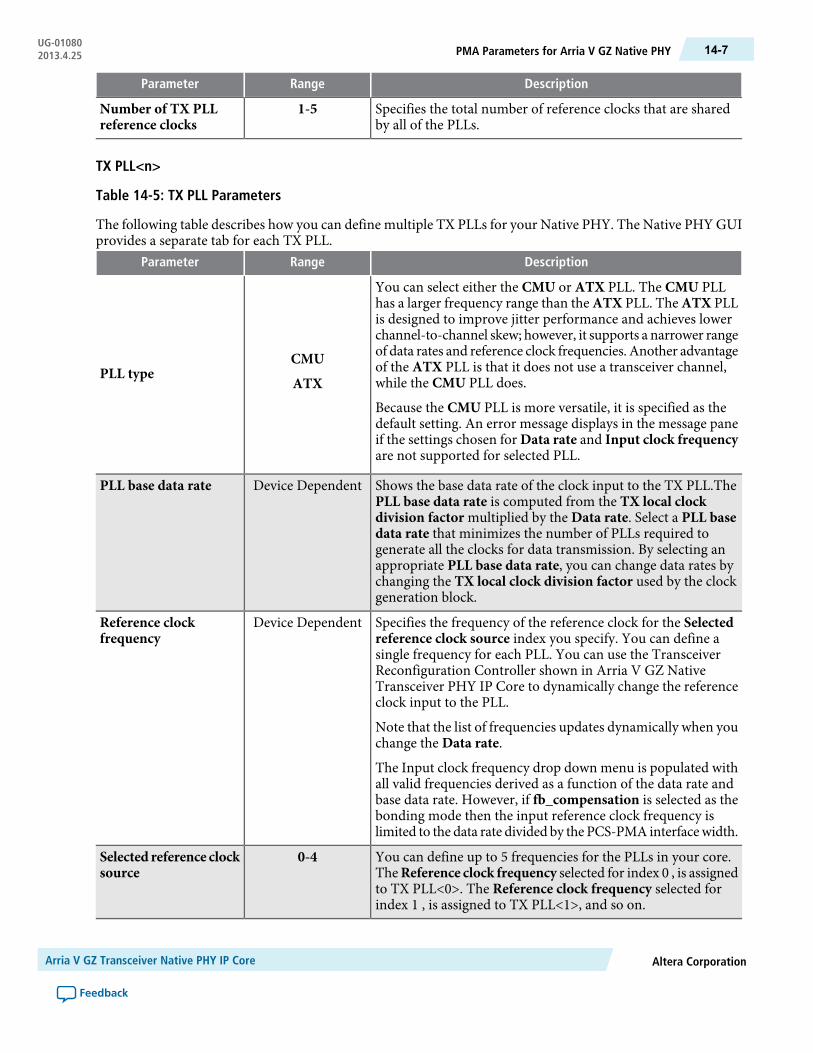
DescriptionRangeParameter
Specifies the total number of reference clocks that are sharedby all of the PLLs.
1-5Number of TX PLLreference clocks
TX PLL<n>
Table 14-5: TX PLL Parameters
The following table describes how you can define multiple TX PLLs for your Native PHY. The Native PHY GUIprovides a separate tab for each TX PLL.
DescriptionRangeParameter
You can select either the CMU or ATX PLL. The CMU PLLhas a larger frequency range than the ATX PLL. The ATX PLLis designed to improve jitter performance and achieves lowerchannel-to-channel skew; however, it supports a narrower rangeof data rates and reference clock frequencies. Another advantageof the ATX PLL is that it does not use a transceiver channel,while the CMU PLL does.
Because the CMU PLL is more versatile, it is specified as thedefault setting. An error message displays in the message paneif the settings chosen for Data rate and Input clock frequencyare not supported for selected PLL.
CMU
ATXPLL type
Shows the base data rate of the clock input to the TX PLL.ThePLL base data rate is computed from the TX local clockdivision factor multiplied by the Data rate. Select a PLL basedata rate that minimizes the number of PLLs required togenerate all the clocks for data transmission. By selecting anappropriate PLL base data rate, you can change data rates bychanging the TX local clock division factor used by the clockgeneration block.
Device DependentPLL base data rate
Specifies the frequency of the reference clock for the Selectedreference clock source index you specify. You can define asingle frequency for each PLL. You can use the TransceiverReconfiguration Controller shown in Arria V GZ NativeTransceiver PHY IP Core to dynamically change the referenceclock input to the PLL.
Note that the list of frequencies updates dynamically when youchange the Data rate.
The Input clock frequency drop down menu is populated withall valid frequencies derived as a function of the data rate andbase data rate. However, if fb_compensation is selected as thebonding mode then the input reference clock frequency islimited to the data rate divided by the PCS-PMA interfacewidth.
Device DependentReference clockfrequency
You can define up to 5 frequencies for the PLLs in your core.TheReference clock frequency selected for index 0 , is assignedto TX PLL<0>. The Reference clock frequency selected forindex 1 , is assigned to TX PLL<1>, and so on.
0-4Selected reference clocksource
Altera CorporationArria V GZ Transceiver Native PHY IP Core
Feedback
14-7PMA Parameters for Arria V GZ Native PHYUG-010802013.4.25

RX CDR Options
Table 14-6: RX PMA Parameters
The following table describes the RXCDRoptions you can specify. Formore information about theCDR circuitry,refer to the Receiver Clock Data Recovery Unit section in Clock Networks and PLLs in Arria V Devices.
DescriptionRangeParameter
When you turn this option On, you can dynamically changethe reference clock input the CDR circuit. This option is alsorequired to simulate TX PLL reconfiguration.
On/OffEnable CDR dynamicreconfiguration
Specifies the number of reference clocks for the CDRs.1-5Number of CDRreference clocks
Specifies the index of the selected CDR reference clock.0-4SelectedCDRreferenceclock
Specifies the frequency of the clock input to the CDR.Device DependentSelectedCDRreferenceclock frequency
Specifies the maximum PPM difference the CDR can toleratebetween the input reference clock and the recovered clock.
Device DependentPPMdetector threshold
When you turn this option On, the RX parallel clock which isrecovered from the serial received data is an output of the PMA.
On/OffEnable rx_pma_clkoutport
When you turn this option On, the rx_is_lockedtodataport is an output of the PMA.On/OffEnable
rx_is_lockedtodataport
When you turn this option On, the rx_is_lockedtorefport is an output of the PMA.
On/OffEnablerx_is_lockedtoref port
When you turn this option On, the rx_set_lockedtdataand rx_set_lockedtoref ports are outputs of the PMA.
On/OffEnablerx_set_lockedtodataand rx_set_locktorefports
When you turn this option On, the rx_pma_bitslip is aninput to the core. The deserializer slips one clock edge each timethis signal is asserted. You can use this feature to minimizeuncertainty in the serialization process as required by protocolsthat require a datapathwith deterministic latency such as CPRI.
On/OffEnablerx_pma_bitslip_port
When you turn this option On, the rx_seriallpbken isan input to the core. When your drive a 1 on this input port,the PMA operates in loopback mode with TX data looped backto the RX channel.
On/OffEnable rx_seriallpbkenport
Arria V GZ Transceiver Native PHY IP CoreAltera Corporation
Feedback
UG-01080PMA Parameters for Arria V GZ Native PHY14-8 2013.4.25
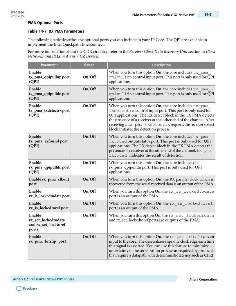
PMA Optional Ports
Table 14-7: RX PMA Parameters
The following table describes the optional ports you can include in your IP Core. The QPI are available toimplement the Intel Quickpath Interconnect.
For more information about the CDR circuitry, refer to the Receiver Clock Data Recovery Unit section in ClockNetworks and PLLs in Arria V GZ Devices.
DescriptionRangeParameter
When you turn this option On, the core includes tx_pma_qpipullup control input port. This port is only used for QPIapplications.
On/OffEnabletx_pma_qpipullupport(QPI)
When you turn this option On, the core includes tx_pma_qpipulldn control input port. This port is only used for QPIapplications.
On/OffEnabletx_pma_qpipulldnport(QPI)
When you turn this option On, the core includes tx_pma_txdetectrx control input port. This port is only used forQPI applications. The RX detect block in the TX PMA detectsthe presence of a receiver at the other end of the channel. Afterreceiving atx_pma_txdetectrx request, the receiver detectblock initiates the detection process.
On/OffEnabletx_pma_txdetectrxport(QPI)
When you turn this option On, the core includes tx_pma_rxfound output status port. This port is only used for QPIapplications. The RX detect block in the TX PMA detects thepresence of a receiver at the other end of the channel.tx_pma_rxfound indicates the result of detection.
On/OffEnabletx_pma_rxfound port(QPI)
When you turn this option On, the core includes therx_pma_qpipulldn port. This port is only used for QPIapplications.
On/OffEnablerx_pma_qpipulldnport(QPI)
When you turn this option On, the RX parallel clock which isrecovered from the serial received data is an output of the PMA.
On/OffEnable rx_pma_clkoutport
When you turn this option On, the rx_is_lockedtodataport is an output of the PMA.
On/OffEnablerx_is_lockedtodataport
When you turn this option On, the rx_is_lockedtorefport is an output of the PMA.
On/OffEnablerx_is_lockedtoref port
When you turn this option On, the rx_set_lockedtdataand rx_set_lockedtoref ports are outputs of the PMA.
On/OffEnablerx_set_lockedtodataand rx_set_locktorefports
When you turn this option On, the rx_pma_bitslip is aninput to the core. The deserializer slips one clock edge each timethis signal is asserted. You can use this feature to minimizeuncertainty in the serialization process as required by protocolsthat require a datapathwith deterministic latency such as CPRI.
On/OffEnablerx_pma_bitslip_port
Altera CorporationArria V GZ Transceiver Native PHY IP Core
Feedback
14-9PMA Parameters for Arria V GZ Native PHYUG-010802013.4.25

DescriptionRangeParameter
When you turn this option On, the rx_seriallpbken isan input to the core. When your drive a 1 on this input port,the PMA operates in loopback mode with TX data looped backto the RX channel.
On/OffEnable rx_seriallpbkenport
The following table lists the best case latency for the most significant bit of a word for the RX deserializerfor the PMA Direct datapath. For example, for an 8-bit interface width, the latencies in UI are 11 for bit 7,12 for bit 6, 13 for bit 5, and so on.
Table 14-8: Latency for RX Deserialization in Arria V GZ Devices
Arria V GZ Latency in UIFPGA Fabric Interface Width
118 bits
1310 bits
1916 bits
2320 bits
3532 bits
4340 bits
9964 bits
12380 bits
Table 14-9: Latency for TX Serialization in Arria V GZ Devices
The following table lists the best- case latency for the LSB of the TX serializer for all supported interface widthsfor the PMA Direct datapath.
Arria V GZ Latency in UIFPGA Fabric Interface Width
448 bits
5410 bits
6816 bits
8420 bits
10032 bits
12440 bits
13264 bits
16480 bits
The following tables lists the bits used for all FPGA fabric to PMA interface widths. Regardless of the FPGAFabric Interface Width selected, all 80 bits are exposed for the TX and RX parallel data ports. However,depending upon the interface width selected not all bits on the bus will be active. The following table listswhich bits are active for each FPGA Fabric Interface Width selection. For example, if your interface is 16bits, the active bits on the bus are [17:0] and [7:0] of the 80 bit bus. The non-active bits are tied to ground.
Arria V GZ Transceiver Native PHY IP CoreAltera Corporation
Feedback
UG-01080PMA Parameters for Arria V GZ Native PHY14-10 2013.4.25
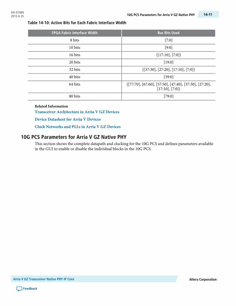
Table 14-10: Active Bits for Each Fabric Interface Width
Bus Bits UsedFPGA Fabric Interface Width
[7:0]8 bits
[9:0]10 bits
{[17:10], [7:0]}16 bits
[19:0]20 bits
{[37:30], [27:20], [17:10], [7:0]}32 bits
[39:0]40 bits
{[77:70], [67:60], [57:50], [47:40], [37:30], [27:20],[17:10], [7:0]}
64 bits
[79:0]80 bits
Related InformationTransceiver Architecture in Arria V GZ Devices
Device Datasheet for Arria V Devices
Clock Networks and PLLs in Arria V GZ Devices
10G PCS Parameters for Arria V GZ Native PHYThis section shows the complete datapath and clocking for the 10G PCS and defines parameters availablein the GUI to enable or disable the individual blocks in the 10G PCS.
Altera CorporationArria V GZ Transceiver Native PHY IP Core
Feedback
14-1110G PCS Parameters for Arria V GZ Native PHYUG-010802013.4.25

Figure 14-3: The 10G PCS datapath
FPGAFabric
Transmitter 10G PCS
Receiver 10G PCS
Transmitter PMA
Receiver PMA
TX FIFO
RX
FIFO
Interla
ken
Fram
eGen
erator
Interla
kenCRC32
Gen
erator
Interla
kenCRC32
Che
cker
64B/66B
Encod
eran
dTX
SM
64B/66B
Decod
eran
dRXSM
Scram
bler
Descram
bler
Interla
ken
Dispa
rityChe
cker
Block
Synchronizer
Interla
ken
Fram
eSynchronizer
Interla
kenDispa
rity
Gen
erator
TXGea
rBox
RX
Gea
rBox
64
64
Parallel Clock (Recovered)
Parallel Clock
40
Serializer
Deserializer
CDR
tx_serial_da
tarx_serial_da
ta
1-bit Ctrl/Data
1 bit Ctrl/Data40
Clock Divider
BER
Parallel and Serial Clocks (From the ×6 or ×N Clock Lines)Serial Clock(From the ×1 Clock Lines)
Central/ Local Clock Divider
Parallel ClockSerial ClockParallel and Serial Clocks
CMU PLL
tx_10g_coreclkin
rx_10g_coreclkin
tx_10g_clkout
rx_10g_clkout
Table 14-11: General and Datapath Parameters
DescriptionRangeParameter
Specifies the protocol that you intend to implementwith the Native PHY. The protocol mode selectedguides theMegaWizard in identifying legal settingsfor the 10G PCS datapath. Use the followingguidelines to select a protocol mode:
• basic : Select this mode for when none of theother options are appropriate. You should alsoselect this mode to enable diagnostics, such asloopback.
• interlaken: Select this mode if you intend toimplement Interlaken.
• sfi5 : Select this mode if you intend toimplement the SERDES Framer Interface Level5 protocol.
• teng_baser : select this mode if you intend toimplement the 10GBASE-R protocol.
• teng_sdi : 10G SDI
basic
interlaken
sfi5
teng_baser
teng_sdi
10G PCS protocol mode
Arria V GZ Transceiver Native PHY IP CoreAltera Corporation
Feedback
UG-0108010G PCS Parameters for Arria V GZ Native PHY14-12 2013.4.25
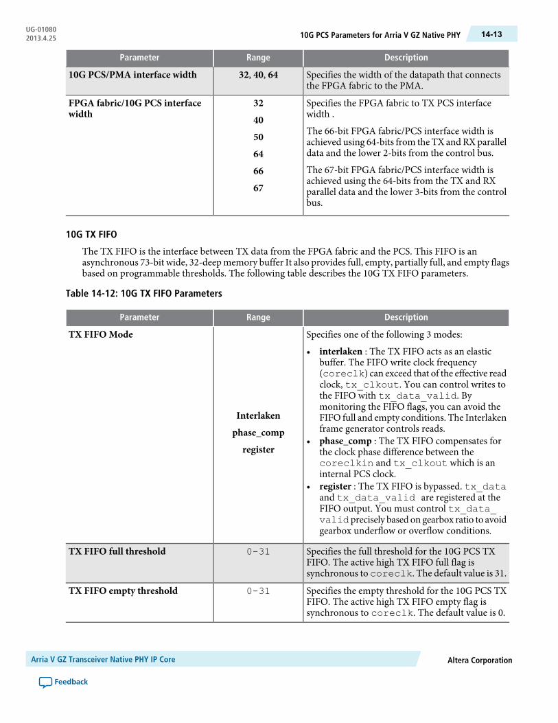
DescriptionRangeParameter
Specifies the width of the datapath that connectsthe FPGA fabric to the PMA.
32, 40, 6410G PCS/PMA interface width
Specifies the FPGA fabric to TX PCS interfacewidth .
The 66-bit FPGA fabric/PCS interface width isachieved using 64-bits from the TX andRXparalleldata and the lower 2-bits from the control bus.
The 67-bit FPGA fabric/PCS interface width isachieved using the 64-bits from the TX and RXparallel data and the lower 3-bits from the controlbus.
32
40
50
64
66
67
FPGA fabric/10G PCS interfacewidth
10G TX FIFO
The TX FIFO is the interface between TX data from the FPGA fabric and the PCS. This FIFO is anasynchronous 73-bit wide, 32-deep memory buffer It also provides full, empty, partially full, and empty flagsbased on programmable thresholds. The following table describes the 10G TX FIFO parameters.
Table 14-12: 10G TX FIFO Parameters
DescriptionRangeParameter
Specifies one of the following 3 modes:
• interlaken : The TX FIFO acts as an elasticbuffer. The FIFO write clock frequency(coreclk) can exceed that of the effective readclock, tx_clkout. You can control writes tothe FIFO with tx_data_valid. Bymonitoring the FIFO flags, you can avoid theFIFO full and empty conditions. The Interlakenframe generator controls reads.
• phase_comp : The TX FIFO compensates forthe clock phase difference between thecoreclkin and tx_clkout which is aninternal PCS clock.
• register : The TX FIFO is bypassed. tx_dataand tx_data_valid are registered at theFIFO output. You must control tx_data_validprecisely based on gearbox ratio to avoidgearbox underflow or overflow conditions.
Interlaken
phase_comp
register
TX FIFO Mode
Specifies the full threshold for the 10G PCS TXFIFO. The active high TX FIFO full flag issynchronous tocoreclk. The default value is 31.
0-31TX FIFO full threshold
Specifies the empty threshold for the 10G PCS TXFIFO. The active high TX FIFO empty flag issynchronous to coreclk. The default value is 0.
0-31TX FIFO empty threshold
Altera CorporationArria V GZ Transceiver Native PHY IP Core
Feedback
14-1310G PCS Parameters for Arria V GZ Native PHYUG-010802013.4.25

DescriptionRangeParameter
Specifies the partially full threshold for the 10GPCS TX FIFO. The active high TX FIFO partiallyfull flag is synchronous to coreclk. The defaultvalue is 23.
0-31TX FIFO partially full threshold
Specifies the partially empty threshold for the 10GPCS TX FIFO. The active high TX FIFO partiallyempty flag is synchronous to coreclk.
0-31TXFIFOpartially empty threshold
When you turn this option On , the 10G PCSincludes the active high tx_10g_fifo_fullport. tx_10g_fifo_full is synchronous tocoreclk.
On/OffEnable tx_10g_fifo_full port
When you turn this option On , the 10G PCSincludes the active high tx_10g_fifo_pfullport. tx_10g_fifo_pfull is synchronousto coreclk.
On/OffEnable tx_10g_fifo_pfull port
When you turn this option On, the 10G PCSincludes the active high tx_10g_fifo_emptyport. tx_10g_fifo_empty is pulse-stretched.It is asynchronous to coreclk and synchronousto tx_clkout which is the read clock.
On/OffEnable tx_10g_fifo_empty port
When you turn this option On, the 10G PCSincludes the tx_10g_fifo_pempty port.
On/OffEnable tx_10g_fifo_pempty port
When you turn this option On, the 10G PCSincludes the active high tx_10g_fifo_delport. This signal is asserted when a word is deletedfrom the TX FIFO. This signal is only used for the10GBASE-R protocol.
On/OffEnable tx_10g_fifo_del port(10GBASE-R)
When you turn this option On, the 10G PCSincludes the active hightx_10g_fifo_insertport. This signal is asserted when a word is insertedinto the TX FIFO. This signal is only used for the10GBASE-R protocol.
On/OffEnable tx_10g_fifo_insert port(10GBASE-R)
10G RX FIFO
The RX FIFO is the interface between RX data from the FPGA fabric and the PCS. This FIFO is anasynchronous 73-bit wide, 32-deep memory buffer It also provides full, empty, partially full, and empty flagsbased on programmable thresholds. The following table describes the 10G RX FIFO parameters.
Arria V GZ Transceiver Native PHY IP CoreAltera Corporation
Feedback
UG-0108010G PCS Parameters for Arria V GZ Native PHY14-14 2013.4.25

Table 14-13: 10G RX FIFO Parameters
DescriptionRangeParameter
Specifies one of the following 3 modes:
• interlaken : Select this mode for the Interlakenprotocol. To implement the deskew process. Inthis mode the FIFO acts as an elastic buffer. TheFIFO write clock can exceed the read clock.Your implementation must control the FIFOwrite (tx_datavalid) by monitoring theFIFO flags. The read enable is controlled by theInterlaken Frame Generator.
• clk_comp : This mode compensates for theclock difference between the PLD clock(coreclkin) and rxclkout. After blocklock is achieved, idle ordered set insertions anddeletions compensate for the clock differencebetween RX PMA clock and PLD clock up to ±100 ppm.
• phase_comp : This mode compensates for theclock phase difference between the PLD clock(coreclkin) andrxclkout. Use thismodefor 10GBASE-R.
• register : The TX FIFO is bypassed. rx_dataand rx_data_valid are registered at theFIFO output.
Interlaken
clk_comp
phase_comp
register
TX FIFO Mode
Specifies the full threshold for the 10G PCS RXFIFO. The default value is 31.
0-31RX FIFO full threshold
Specifies the empty threshold for the 10G PCS RXFIFO. The default value is 0.
0-31RX FIFO empty threshold
Specifies the partially full threshold for the 10GPCS RX FIFO. The default value is 23.
0-31RX FIFO partially full threshold
Specifies the partially empty threshold for the 10GPCS RX FIFO.
0-31RXFIFOpartially empty threshold
When you turn this option On, the RX FIFO alsoperforms deskew. This option is only available forthe Interlaken protocol.
On/ OffEnable RX FIFO deskew(interlaken)
When you turn this optionOn, all alignmentwords(sync words), including the first sync word, areremoved after frame synchronization is achieved.If you enable this option, you must also enablecontrol word deletion.
On/OffEnable RX FIFO alignment worddeletion (interlaken)
Altera CorporationArria V GZ Transceiver Native PHY IP Core
Feedback
14-1510G PCS Parameters for Arria V GZ Native PHYUG-010802013.4.25

DescriptionRangeParameter
When you turn this option On , the rx_control_del parameter enables or disableswriting the Interlaken control word to RX FIFO.When disabled, a value of 0 for rx_control_del writes all control words to RX FIFO. Whenenabled, a value of 1 deletes all control words andonly writes the data to the RX FIFO.
On/OffEnable RX FIFO control worddeletion (interlaken)
When you turn this option On, the 10G PCSincludes the rx_data_valid signal whichIndicates when rx_data is valid. This option isavailable when you select the following parameters:
• 10G PCS protocol mode is Interlaken• 10G PCS protocol mode is Basic and RX FIFO
mode is phase_comp• 10G PCS protocol mode is Basic and RX FIFO
mode is register
On/OffEnable rx_10g_fifo_data_validport
When you turn this option On, the 10G PCSincludes the active high rx_10g_fifo_fullport. rx_10g_fifo_full is synchronous torx_clkout.
On/OffEnable rx_10g_fifo_full port
When you turn this option On, the 10G PCSincludes the active high rx_10g_fifo_pfullport. rx_10g_fifo_pfull is synchronous torx_clkout.
On/OffEnable rx_10g_fifo_pfull port
When you turn this option On, the 10G PCSincludes the active high rx_10g_fifo_emptyport.
On/OffEnable rx_10g_fifo_empty port
When you turn this option On, the 10G PCSincludes the rx_10g_fifo_pempty port.
On/OffEnable rx_10g_fifo_pempty port
When you turn this option On, the 10G PCSincludes therx_10g_fifo_delport. This signalis asserted when a word is deleted from the RXFIFO. This signal is only used for the 10GBASE-Rprotocol.
On/OffEnable rx_10g_fifo_del port(10GBASE-R)
When you turn this option On, the 10G PCSincludes the rx_10g_fifo_insert port. Thissignal is asserted when a word is inserted into theRX FIFO. This signal is only used for the10GBASE-R protocol.
On/OffEnable rx_10g_fifo_insert port(10GBASE-R)
When you turn this option On, the 10G PCSincludes the rx_10g_fifo_rd_en input port.Asserting this signal reads a word from the RXFIFO. This signal is only available for the Interlakenprotocol.
On/OffEnable rx_10g_fifo_rd_en port(Interlaken)
Arria V GZ Transceiver Native PHY IP CoreAltera Corporation
Feedback
UG-0108010G PCS Parameters for Arria V GZ Native PHY14-16 2013.4.25

DescriptionRangeParameter
When you turn this option On, the 10G PCSincludes therx_10g_fifo_align_valoutputport. This signal is asserted when the wordalignment pattern is found. This signal is onlyavailable for the Interlaken protocol.
On/OffEnable rx_10g_fifo_align_val port(Interlaken)
When you turn this option On, the 10G PCSincludes a divide by 33 clock output port. Youtypically need this option when the fabric to PCSinterface width is 66. Check location - moved toRX FIFO, but I don't know where
On/Offenable rx10g_clk33out port
When you turn this option On, the 10G PCSincludes the rx_10g_fifo_align_clr inputport. When this signal is asserted, the FIFO resetsand begins searching for a new alignment pattern.This signal is only available for the Interlakenprotocol.
On/OffEnable rx_10g_fifo_align_clr port(Interlaken)
When you turn this option On, the 10G PCSincludes the rx_10g_fifo_align_en inputport. This signal is used for FIFO deskew forInterlaken. When asserted, the correspondingchannel is enabled for alignment. This signal is onlyavailable for the Interlaken protocol.
On/OffEnable rx_10g_fifo_align_en port(Interlaken)
Interlaken Frame Generator
TX Frame generator generates the metaframe. It encapsulates the payload from MAC with the framing layercontrol words, including sync, scrambler, skip and diagnostic words. The following table describes theInterlaken frame generator parameters.
Table 14-14: Interlaken Frame Generator Parameters
DescriptionRangeParameter
When you turn this optionOn, the frame generatorblock of the 10G PCS is enabled.
On/Offteng_tx_framgen_enable
Specifies the metaframe length.0-8192teng_tx_framgen_user_length
When you turn this optionOn, the frame generatorburst functionality is enabled.
On/Offteng_tx_framgen_burst_enable
When you turn this option On, the 10G PCSincludes the tx_10g_frame output port. Whenasserted,tx_10g_frame indicates the beginningof a new metaframe inside the frame generator.
On/OffEnable tx_10g_frame port
Altera CorporationArria V GZ Transceiver Native PHY IP Core
Feedback
14-1710G PCS Parameters for Arria V GZ Native PHYUG-010802013.4.25
DescriptionRangeParameter
When you turn this option On, the 10G PCSincludes the tx_10g_frame_diag_status2-bit input port. This port contains the lane StatusMessage from the framing layer Diagnostic Word,bits[33:32]. This message is inserted into the nextDiagnosticWord generated by the frame generationblock. The message must be held static for 5 cyclesbefore and 5 cycles after the tx_frame pulse.
On/OffEnable tx_10g_frame_diag_statusport
When you turn this option On, the 10G PCSincludes the tx_10g_frame_burst_en inputport. This port controls frame generator data readsfrom the TX FIFO. The value of this signal islatched once at the beginning of each Metaframe.It controls whether data is read from the TX FIFOor SKIP Words are inserted for the currentMetaframe. Itmust be held static for 5 cycles beforeand 5 cycles after thetx_frame pulse.Whentx_10g_frame_burst_en is 0, the framegeneratordoes not read data from the TX FIFO for currentMetaframe. It insert SKIPs. When tx_10g_frame_burst_en is 1, the frame generator readsdata from the TX FIFO for current Metaframe.
On/OffEnable tx_10g_frame_burst_enport
Interlaken Frame Synchronizer
The Interlaken frame synchronizer block achieves lock by looking for four synchronization words inconsecutive metaframes. After synchronization, the frame synchronizer monitors the scrambler word in themetaframe and deasserts the lock signal after three consecutive mismatches and starts the synchronizationprocess again. Lock status is available to the FPGA fabric. The following table describes the Interlaken framesynchronizer parameters.
Table 14-15: Interlaken Frame Synchronizer Parameters
DescriptionRangeParameter
When you turn this optionOn, the 10GPCS framegenerator is enabled.
On/Offteng_tx_framsync_enable
When you turn this option On, the 10G PCSincludes the rx_10g_frame output port. Thissignal is asserted to indicate the beginning of a newmetaframe inside.
On/OffEnable rx_10g_frame port
When you turn this option On, the 10G PCSincludes therx_10g_frame_lock output port.This signal is asserted to indicate that the framesynchronization state machine has achieved framelock.
On/OffEnable rx_10g_frame_lock_port
Arria V GZ Transceiver Native PHY IP CoreAltera Corporation
Feedback
UG-0108010G PCS Parameters for Arria V GZ Native PHY14-18 2013.4.25
DescriptionRangeParameter
When you turn this option On, the 10G PCSincludes therx_10g_frame_mfrm_erroutputport. This signal is asserted to indicate anmetaframe error.
On/OffEnable rx_10g_frame_mfrm_errport
When you turn this option On, the 10G PCSincludes therx_10g_frame_sync_erroutputport. This signal is asserted to indicatesynchronization control word errors. This signalremains asserted during the loss of block_lock anddoes not update until block_lock is recovered.
On/OffEnable rx_10g_frame_sync_errport
When you turn this option On, the 10G PCSincludes therx_10g_frame_skip_insoutputport. This signal is asserted to indicate a SKIP wordwas received by the frame sync in a non-SKIPwordlocation within the metaframe.
On/OffEnable rx_10g_frame_skip_insport
When you turn this option On, the 10G PCSincludes therx_10g_frame_pyld_insoutputport. This signal is asserted to indicate a SKIP wordwas not received by the frame sync in a SKIP wordlocation within the metaframe.
On/OffEnable rx_10g_frame_pyld_insport
When you turn this option On, the 10G PCSincludes therx_10g_frame_skip_erroutputport. This signal is asserted to indicate the framesynchronization has received an erroneous wordin a Skip control word location within theMetaframe. This signal remains asserted during theloss of block_lock and does update until block_lockis recovered.
On/OffEnable rx_10g_frame_skip_errport
When you turn this option On, the 10G PCSincludes therx_10g_frame_diag_erroutputport. This signal is asserted to indicate a diagnosticcontrol word error. This signal remains assertedduring the loss of block_lock and does update untilblock_lock is recovered.
On/OffEnable rx_10g_frame_diag_errport
When you turn this option On, the 10G PCSincludes the rx_10g_frame_diag_status2-bit output port per channel. This port containsthe lane Status Message from the framing layerDiagnostic Word, bits[33:32]. This message isinserted into the next Diagnostic Word generatedby the frame generation block.
On/OffEnable rx_10g_frame_diag_statusport
Interlaken CRC32 Generator and Checker
CRC-32 provides a diagnostic tool on a per-lane basis. You can use CRC-32 to trace interface errors backto an individual lane. The CRC-32 calculation covers the whole metaframe including the Diagnostic Worditself. This CRC code value is stored in the CRC32 field of theDiagnosticWord. The following table describesthe CRC-32 parameters.
Altera CorporationArria V GZ Transceiver Native PHY IP Core
Feedback
14-1910G PCS Parameters for Arria V GZ Native PHYUG-010802013.4.25

Table 14-16: Interlaken CRC32 Generator and Checker Parameters
DescriptionRangeParameter
When you turn this option On, the TX 10G PCSdatapath includes the CRC32 function.
On/OffEnable Interlaken TX CRC32Generator
When you turn this option On, the RX 10G PCSdatapath includes the CRC32 function.
On/OffEnable Interlaken RX CRC32Generator
When you turn this option On, the 10G PCSincludes the rx_10g_crc32_err port. Thissignal is asserted to indicate that the CRC checkerhas found an error in the current metaframe.
On/OffEnable rx_10g_crc32_err port
10GBASE-R BER Checker
The BERmonitor block conforms to the 10GBASE-R protocol specification as described in IEEE 802.3-2008Clause-49. After block lock is achieved, the BERmonitor starts to count the number of invalid synchronizationheaders within a 125-ms period. If more than 16 invalid synchronization headers are observed in a 125-msperiod, the BER monitor provides the status signal to the FPGA fabric, indicating a high bit error. Thefollowing table describes the 10GBASE-R BER checker parameters.
Table 14-17: 10GBASE-R BER Checker Parameters
DescriptionRangeParameter
When you turn this option On, the TX 10G PCSdatapath includes therx_10g_highber outputport. This signal is asserted to indicate a BER of>10 4 . A count of 16 errors in 125- m s periodindicates a BER > 10 4 . This signal is only availablefor the 10GBASE-R protocol.
On/OffEnable rx_10g_highber port(10GBASE-R)
When you turn this option On, the TX 10G PCSdatapath includes therx_10g_highber_clr_cnt input port. When asserted, the BER counterresets to 0. This signal is only available for the10GBASE-R protocol.
On/OffEnable rx_10g_highber_clr_cntport (10GBASE-R)
When you turn this option On, the 10G PCSincludes the rx_10g_clr_errblk_countinput port.When asserted, error block counter thatcounts the number of RX errors resets to 0. Thissignal is only available for the 10GBASE-Rprotocol.
On/OffEnable rx_10g_clr_errblk_countport (10GBASE-R)
64b/66b Encoder and Decoder
The 64b/66b encoder and decoder conform to the 10GBASE-R protocol specification as described in IEEE802.3-2008 Clause-49. The 64b/66b encoder sub-block receives data from the TX FIFO and encodes the64-bit data and 8-bit control characters to the 66-bit data block required by the 10GBASE-R protocol. Thetransmit state machine in the 64b/66b encoder sub-block checks the validity of the 64-bit data from theMAC layer and ensures proper block sequencing.
Arria V GZ Transceiver Native PHY IP CoreAltera Corporation
Feedback
UG-0108010G PCS Parameters for Arria V GZ Native PHY14-20 2013.4.25
The 64b/66b decoder sub-block converts the received data from the descrambler into 64-bit data and 8-bitcontrol characters. The receiver state machine sub-block monitors the status signal from the BER monitor.The following table describes the 64/66 encoder and decoder parameters.
Table 14-18: 64b/66b Encoder and Decoder Parameters
DescriptionRangeParameter
When you turn this option On, the 10G PCS records.This parameter is valid for the Interlaken and10GBASE-R protocols.
On/OffEnable TX sync header errorinsertion
When you turn this option On, the 10G PCS includesthe TX 64b/66b encoder.
On/OffEnable TX 64b/66b encoder
When you turn this option On, the 10G PCS includesthe RX 64b/66b decoder.
On/OffEnable TX 64b/66b encoder
Scrambler and Descrambler Parameters
TX scrambler randomizes data to create transitions to create DC-balance and facilitate CDR circuits basedon the x58 + x39 +1 polynomial. The scrambler operates in the following two modes:
• Synchronous—The Interlaken protocol requires synchronous mode.• Asynchronous (also called self-synchronized)—The 10GBASE-R protocol requires thismode as specified
in IEEE 802.3-2008 Clause-49.
The descrambler block descrambles received data to regenerate unscrambled data using the x58+x39+1polynomial. The following table describes the scrambler and descrambler parameters.
Table 14-19: Scrambler and Descrambler Parameters
DescriptionRangeParameter
When you turn this option On, the TX 10G PCSdatapath includes the scrambler function. Thisoption is available for the Interlaken and10GBASE-R protocols.
On/OffEnable TX scrambler
You must provide a different seed for each lane.This parameter is only required for the Interlakenprotocol.
User-specified 15-bitvalue
TX scrambler seed
When you turn this option On, the RX 10G PCSdatapath includes the scrambler function. Thisoption is available for the Interlaken and10GBASE-R protocols.
On/OffEnable RX scrambler
When you turn this option On, the 10G PCSincludes the rx_10g_descram_err port.
On/OffEnable rx_10g_descram_err port
Interlaken Disparity Generator and Checker
The Disparity Generator monitors the data transmitted to ensure that the running disparity remains withina ±96-bit bound. It adds the 67th bit to indicate whether or not the data is inverted. The Disparity Checkermonitors the status of the 67th bit of the incoming word to determine whether or not to invert bits[63:0] ofthe received word. The following table describes Interlaken disparity generator and checker parameters.
Altera CorporationArria V GZ Transceiver Native PHY IP Core
Feedback
14-2110G PCS Parameters for Arria V GZ Native PHYUG-010802013.4.25

Table 14-20: Interlaken Disparity Generator and Checker Parameters
DescriptionRangeParameter
When you turn this option On, the 10G PCSincludes the disparity generator. This option isavailable for the Interlaken protocol.
On/OffEnable Interlaken TX disparitygenerator
When you turn this option On, the 10G PCSincludes the disparity checker. This option isavailable for the Interlaken protocol.
On/OffEnable Interlaken RX disparitygenerator
Block Synchronization
The block synchronizer determines the block boundary of a 66-bit word for the 10GBASE-R protocol or a67-bit word for the Interlaken protocol. The incoming data stream is slipped one bit at a time until a validsynchronization header (bits 65 and 66) is detected in the received data stream. After the predefined numberof synchronization headers is detected, the block synchronizer asserts rx_10g_blk_lock to otherreceiver PCS blocks down the receiver datapath and to the FPGA fabric. The block synchronizer is designedin accordance with both the Interlaken protocol specification and the 10GBASE-R protocol specification asdescribed in IEEE 802.3-2008 Clause-49.
Table 14-21: Bit Reversal and Polarity Inversion Parameters
DescriptionRangeParameter
When you turn this option On, the 10G PCSincludes the RX block synchronizer. This option isavailable for the Interlaken and 10GBASE-Rprotocols.
On/OffEnable RX block synchronizer
When you turn this option On, the 10G PCSincludes the rx_10G_blk_lock output port.This signal is asserted to indicate the receiver hasachieved block synchronization. This option isavailable for the Interlaken, 10GBASE-R, and otherprotocols that user the PCS lock state machine toachieve and monitor block synchronization.
On/OffEnable rx_10g_blk_lock port
When you turn this option On, the 10G PCSincludes therx_10G_blk_sh_err output port.This signal is asserted to indicate that an invalidsync header has been received. This signal is activeafter block lock is achieved. This option is availablefor the Interlaken, 10GBASE-R, and other protocolsthat user the PCS lock statemachine to achieve andmonitor block synchronization.
On/OffEnable rx_10g_blk_sh_err port
Gearbox
The gearbox adapts the PMA data width to a wider PCS data width when the PCS is not two or four timesthe PMA width.
Arria V GZ Transceiver Native PHY IP CoreAltera Corporation
Feedback
UG-0108010G PCS Parameters for Arria V GZ Native PHY14-22 2013.4.25

Table 14-22: Gearbox Parameters
DescriptionRangeParameter
When you turn this optionOn, the gearbox invertsthe polarity of TX data allowing you to correctincorrect placement and routing on the PCB.
On/OffEnable TX data polarity inversion
When you turn this option On, the TX gearboxoperates in bitslip mode.
On/OffEnable TX data bitslip
When you turn this optionOn, the gearbox invertsthe polarity of RX data allowing you to correctincorrect placement and routing on the PCB.
On/OffEnable RX data polarity inversion
When you turn this option On, the 10G PCS RXblock synchronizer operates in bitslip mode.
On/OffEnable RX data bitslip
When you turn this option On, the 10G PCSincludes the tx_10g_bitslip input port. Thedata slips 1 bit for every positive edge of the tx_10g_bitslip input. The maximum shift is <pcswidth> -1 bits, so that if the PCS is 64 bits wide,you can shift 0-63 bits.
On/OffEnable tx_10g_bitslip port
When you turn this option On, the 10G PCSincludes the rx_10g_bitslip input port. Thedata slips 1 bit for every positive edge of the rx_10g_bitslip input. he maximum shift is <pcswidth> -1 bits, so that if the PCS is 64 bits wide,you can shift 0-63 bits.
On/OffEnable rx_10g_bitslip port
Related InformationTransceiver Archictecture in Arria V GZ Devices
Interfaces for Arria V GZ Native PHYThis section describes the interfaces available for the Arria V GZ native PHY.
The Native PHY includes several interfaces that are common to all parameterizations. It also has separateinterfaces for the Standard and 10G PCS datapaths. If you use dynamic reconfiguration to change betweenthe Standard and 10G PCS datapaths, your top-level HDL file includes the port for both the Standard and10G PCS datapaths. In addition, the Native PHY allows you to enable ports, even for disabled blocks tofacilitate dynamic reconfiguration.
The Native PHY uses the following prefixes for port names:
• Standard PCS ports—tx_std_, rx_std_• 10G PCS ports—tx_10g_, rx_10g_• PMA ports—tx_pma_, rx_pma_
Altera CorporationArria V GZ Transceiver Native PHY IP Core
Feedback
14-23Interfaces for Arria V GZ Native PHYUG-010802013.4.25

The port descriptions use the following variables to represent parameters:
• <n>—The number of lanes• <p>—The number of PLLs• <r>—the number of CDR references clocks selected
Common Interface Ports for Arria V GZ Native PHYThis section describes the interface ports for the Arria V GZ native PHY.
Common interface consists of reset, clock signals, serial interface ports, control and status ports, paralleldata ports, PMA ports and reconfig interface ports. The following figure illustrates these ports.
Figure 14-4: Arria V GZ Native PHY Common Interfaces
tx_pll_refclk[<r>-1:0]tx_pma_clkout[<n>-1:0]rx_pma_clkout[<n>-1:0]rx_clklow[<n>-1:0]rx_fref[<n>-1:0]rx_cdr_refclk[<r>-1:0]
Clock Input& Output Signals
rx_seriallpbken[<n>-1:0]rx_setlocktodata[<n>-1:0]rx_setlocktoref[<n>-1:0]
pll_locked[<p>-1:0]rx_is_lockedtodata[<n>-1:0]rx_is_lockedtoref[<n>-1:0]
rx_clkslip[<n>-1:0]
Control &Status Portspll_powerdown[<p>-1:0]
tx_analogreset[<n>-1:0]tx_digitalreset[<n>-1:0]rx_analogreset[<n>-1:0]rx_digitalreset[<n>-1:0]
Resets
QPI
tx_pma_parallel_data[<n>80-1:0]rx_pma_parallel_data[<n>80-1:0]tx_parallel_data[<n>64-1:0]rx_parallel_data[<n>64-1:0]
tx_pma_qpipulluptx_pma_qpipulldntx_pma_txdetectrxtx_pma_rxfoundrx_pma_qpipulldn
ParallelData Ports
tx_serial_data[<n>-1:0]rx_serial_data[<n>-1:0]
TX & RXSerial Ports
reconfig_to_xcvr [(<n>70-1):0]reconfig_from_xcvr [(<n>46-1):0]
tx_cal_busy[<n>-1:0]rx_cal_busy[<n>-1:0]
ReconfigurationInterface Ports
Native PHY Common Interfaces
Table 14-23: Native PHY Common Interfaces
DescriptionDirectionName
Clock Inputs and Output Signals
The reference clock input to the TX PLL.Inputtx_pll_refclk
[<r> -1:0]
TX parallel clock output from PMAOutputtx_pma_clkout
[<n> -1:0]
RX parallel clock (recovered clock) output from PMAOutputrx_pma_clkout
[<n> -1:0]
Arria V GZ Transceiver Native PHY IP CoreAltera Corporation
Feedback
UG-01080Common Interface Ports for Arria V GZ Native PHY14-24 2013.4.25

DescriptionDirectionName
The RX parallel recovered clock. You can use this clock as aninput to an external PPM detector.
Outputrx_clklow
[<n> -1:0]
RX phase frequency detector (PFD) reference clock. You can usethis clock as an input to an external PPM detector.
Outputrx_fref
[<n> -1:0]
Input reference clock for the RX PFD circuit.Inputrx_cdr_refclk
[<n> -1:0]
Resets
When asserted, resets the TX PLL. Active high, edge sensitivereset signal. By default, the Arria V GZ Native Transceiver PHYIP Core creates a separate pll_powerdown signal for eachlogical PLL. However, the Fitter may merge the PLLs if they arein the same transceiver bank. PLLs can only be merged if theirpll_powerdown signals are driven from the same source. Ifthe PLLs are in separate transceiver banks, you can choose todrive the pll_powerdown signals separately.
Inputpll_powerdown
[<n> -1:0]
When asserted, resets for TX PMA, TX clock generation block,and serializer. Active high, edge sensitive reset signal.
Inputtx_analogreset
[<n> -1:0]
When asserted, resets the digital components of the TX datapath.Active high, edge sensitive reset signal.If your design includesbonded TX PCS channels, refer to Timing Constraints for ResetSignals when Using Bonded PCS Channels for a SDC constraintyou must include in your design.
Inputtx_digitalreset
[<n> -1:0]
When asserted, resets the RXCDR, deserializer, Active high, edgesensitive reset signal.
Inputrx_analogreset
[<n> -1:0]
When asserted, resets the digital components of the RX datapath.Active high, edge sensitive reset signal.
Inputrx_digitalreset
[<n> -1:0]
Parallel Data Ports
TX parallel data for the PMA Direct datapath. Driven directlyfrom the FPGA fabric to the PMA. Not used when you enableeither the Standard or 10G PCS datapath.
Inputtx_pma_parallel_data
[<n> 80-1:0]
RX PMA parallel data driven from the PMA to the FPGA fabric.Not used when you enable either the Standard or 10G PCSdatapath.
Outputrx_pma_parallel_data
[<n> 80-1:0]
Altera CorporationArria V GZ Transceiver Native PHY IP Core
Feedback
14-25Common Interface Ports for Arria V GZ Native PHYUG-010802013.4.25

DescriptionDirectionName
PCS TX parallel data. Used when you enable either the Standardor 10Gdatapath. For the Standard datapath, if you turn onEnablesimplified data interface , tx_parallel_data includes only the dataand control signals necessary for the current configuration.Dynamic reconfiguration of the interface is not supported. Forthe 10G PCS, if the parallel data interface is less than 64 bits wide,the low-order bits of tx_parallel_data are valid. For the 10G PCSoperating in 66:40 Basic mode, the 66 bus is formed as follows:{ tx_parallel_data[63:0],tx_10g_control[0], tx_10g_control[1]}.
Inputtx_parallel_data
[<n> 64-1:0]
PCS RX parallel data. Used when you enable either the Standardor 10Gdatapath. For the Standard datapath, if you turn onEnablesimplified data interface , rx_parallel_data includes only the dataand control signals necessary for the current configuration.Dynamic reconfiguration of the interface is not supported. Forthe 10G PCS, if the parallel data interface is less than 64 bits wide,the low-order bits of rx_parallel_data are valid. For the 10G PCSoperating in 66:40 mode, the 66 bus is formed as follows: {rx_parallel_data[63:0],rx_10g_control[0], rx_10g_control[1]}.
Outputrx_parallel_data
[<n> 64-1:0]
QPI
QPI control input port. Only for QPI applications.Inputtx_pma_qpipullup
QPI control input port. Only for QPI applications.Inputtx_pma_qpipulldn
When asserted, the RX detect block in the TX PMA detects thepresence of a receiver at the other end of the channel. Afterreceiving a tx_pma_txdetectrx request, the receiver detectblock initiates the detection process. Only for QPI applications.
Inputtx_pma_txdetectrx
Indicates the status of an RX detection in the TX PMA. Only forQPI applications.
Outputtx_pma_rxfound
QPI control input port. Only for QPI applications.Inputrx_pma_qpipulldn
TX and RX Serial Ports
TX differential serial output data.Outputtx_serial_data
[<n> -1:0]
RX differential serial output data.Inputrx_serial_data
[<n> -1:0]
Control and Status Ports
When asserted, the transceiver enters loopback mode. Loopbackdrives TX data to the RX interface.
Inputrx_seriallpbken
[<n> -1:0]
Arria V GZ Transceiver Native PHY IP CoreAltera Corporation
Feedback
UG-01080Common Interface Ports for Arria V GZ Native PHY14-26 2013.4.25

DescriptionDirectionName
When asserted, programs the RX CDR to manual lock to datamode in which you control the reset sequence using the rx_setlocktoref and rx_setlocktodata. Refer to ResetSequence for CDR in Manual Lock Mode in Transceiver ResetControl inArriaVGZDevices formore information aboutmanualcontrol of the reset sequence.
Inputrx_set_locktodata
[<n> -1:0]
Whenasserted, programs theRXCDR tomanual lock to referencemode in which you control the reset sequence using the rx_setlocktoref and rx_setlocktodata. Refer to ResetSequence for CDR in Manual Lock Mode in Transceiver ResetControl inArriaVGZDevices formore information aboutmanualcontrol of the reset sequence.
Inputrx_set_locktoref
[<n> -1:0]
When asserted, indicates that the PLL is locked to the inputreference clock.
Outputpll_locked
[<p> -1:0]
When asserted, the CDR is locked to the incoming data.Outputrx_is_lockedtodata
[<n> -1:0]
When asserted, the CDR is locked to the incoming referenceclock.
Outputrx_is_lockedtoref
[<n> -1:0]
When asserted, the deserializer slips one clock edge. This signalis used to achieve word alignment.
Inputrx_clkslip
[<n> -1:0]
Reconfig Interface Ports
Reconfiguration signals from the Transceiver ReconfigurationController. <n> grows linearly with the number ofreconfiguration interfaces.
Inputreconfig_to_xcvr
[(<n> 70-1):0]
Reconfiguration signals to the Transceiver ReconfigurationController. <n> grows linearly with the number ofreconfiguration interfaces.
Outputreconfig_from_xcvr
[(<n> 46-1):0]
Reconfiguration status, indicates TX calibration is in progressOutputtx_cal_busy
[<n> -1:0]
Reconfiguration status, indicates RX calibration is in progressOutputrx_cal_busy
[<n> -1:0]
Related InformationTiming Constraints for Reset Signals when Using Bonded PCS Channels on page 17-10
Standard PCS Interface PortsThis section describes the PCS interface.
Altera CorporationArria V GZ Transceiver Native PHY IP Core
Feedback
14-27Standard PCS Interface PortsUG-010802013.4.25
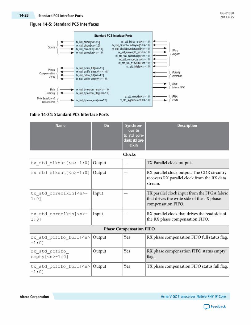
Figure 14-5: Standard PCS Interfaces
ClocksWordAligner
PhaseCompensation
FIFO
ByteOrdering
rx_std_rmfifo_empty[<n>-1:0]rx_std_rmfifo_full[<n>-1:0]
RateMatch FIFO
rx_std_polinv[<n>-1:0]tx_std_polinv[<n>-1:0]
PolarityInversion
PMAPorts
Standard PCS Interface Portsrx_std_bitrev_ena[<n>-1:0]
tx_std_bitslipboundarysel[5<n>-1:0]rx_std_bitslipboundarysel[5<n>-1:0]
rx_std_runlength_err[<n>-1:0]rx_std_wa_patternalign[<n>-1:0]
rx_std_comdet_ena[<n>-1:0]rx_std_wa_a1a2size[<n>-1:0]
rx_std_bitslip[<n>-1:0]
tx_std_elecidle[<n>-1:0]rx_std_signaldetect[<n>-1:0]rx_std_byterev_ena[<n>-1:0]Byte Serializer &
Deserializer
tx_std_clkout[<n>-1:0]rx_std_clkout[<n>-1:0]tx_std_coreclkin[<n>-1:0]rx_std_coreclkin[<n>-1:0]
rx_std_pcfifo_full[<n>-1:0]rx_std_pcfifo_empty[<n>-1:0]tx_std_pcfifo_full[<n>-1:0]tx_std_pcfifo_empty[<n>-1:0]
rx_std_byteorder_ena[<n>-1:0]rx_std_byteorder_flag[<n>-1:0]
Table 14-24: Standard PCS Interface Ports
DescriptionSynchron-ous to
tx_std_core-clkin/rx_std_core-
clkin
DirName
Clocks
TX Parallel clock output.—Outputtx_std_clkout[<n>-1:0]
RX parallel clock output. The CDR circuitryrecovers RX parallel clock from the RX datastream.
—Outputrx_std_clkout[<n>-1:0]
TX parallel clock input from the FPGA fabricthat drives the write side of the TX phasecompensation FIFO.
—Inputtx_std_coreclkin[<n>-1:0]
RX parallel clock that drives the read side ofthe RX phase compensation FIFO.
—Inputrx_std_coreclkin[<n>-1:0]
Phase Compensation FIFO
RX phase compensation FIFO full status flag.YesOutputrx_std_pcfifo_full[<n>-1:0]
RX phase compensation FIFO status emptyflag.
YesOutputrx_std_pcfifo_empty[<n>-1:0]
TX phase compensation FIFO status full flag.YesOutputtx_std_pcfifo_full[<n>-1:0]
Arria V GZ Transceiver Native PHY IP CoreAltera Corporation
Feedback
UG-01080Standard PCS Interface Ports14-28 2013.4.25

DescriptionSynchron-ous to
tx_std_core-clkin/rx_std_core-
clkin
DirName
TX phase compensation FIFO status emptyflag.
YesOutputtx_std_pcfifo_empty[<n>-1:0]
Byte Ordering
Byte ordering enable. When this signal isasserted, the byte ordering block initiates abyte ordering operation if the Byte orderingcontrol mode is set to manual. Once byteordering has occurred, you must deassert andreassert this signal to perform another byteordering operation. This signal is ansynchronous input signal; however, it mustbe asserted for at least 1 cycle of rx_std_clkout.
NoInputrx_std_byteorder_ena[<n>-1:0]
Byte ordering status flag. When asserted,indicates that the byte ordering block hasperformed a byte order operation. This signalis asserted on the clock cycle in which byteordering occurred. This signal is synchronousto the rx_std_clkout clock. You must asynchronizer this signal.
YesOutputrx_std_byteorder_flag[<n>-1:0]
Byte Serializer and Deserializer
This control signal is available in when thePMA width is 16 or 20 bits. When asserted,enables byte reversal on the RX interface.
NoInputrx_std_byterev_ena[<n>-1:0]
8B/10B
Polarity inversion for the 8B/10B decoder,When set, the RX channels invert the polarityof the received data. You can use this signalto correct the polarity of differential pairs ifthe transmission circuitry or board layoutmistakenly swapped the positive and negativesignals. The polarity inversion functionoperates on the word aligner input.
NoInputrx_std_polinv[<n>-1:0]
Polarity inversion, part of 8B10B encoder,When set, the TX interface inverts the polarityof the TX data.
NoInputtx_std_polinv[<n>-1:0]
Altera CorporationArria V GZ Transceiver Native PHY IP Core
Feedback
14-29Standard PCS Interface PortsUG-010802013.4.25

DescriptionSynchron-ous to
tx_std_core-clkin/rx_std_core-
clkin
DirName
Rate Match FIFO
Rate match FIFO empty flag. When asserted,the rate match FIFO is empty.
NoOutputrx_std_rmfifo_empty[<n>-1:0]
Rate match FIFO full flag. When asserted theratematch FIFO is full. Youmust synchronizethis signal.
NoOutputrx_std_rmfifo_full[<n>-1:0]
Word Aligner
When asserted, enables bit reversal on the RXinterface. Bit ordermay be reversed if externaltransmission circuitry transmits the mostsignificant bit first. When enabled, the receivecircuitry receives all words in the reverseorder. The bit reversal circuitry operates onthe output of the word aligner.
NoInputrx_std_bitrev_ena[<n>-1:0]
BitSlip boundary selection signal. Specifies thenumber of bits that the TX bit slipper mustslip.
NoInputtx_std_bitslipboundarysel[5<n>-1:0]
This signal operates when the word aligner isin bitslip word alignmentmode. It reports thenumber of bits that the RX block slipped toachieve deterministic latency.
NoOutputrx_std_bitslipboundarysel[5<n>-1:0]
When asserted, indicates a run lengthviolation. Asserted if the number ofconsecutive 1s or 0s exceeds the numberspecified in the parameter editor GUI.
NoOutputrx_std_runlength_err[<n>-1:0]
Active when you place the word aligner inmanual mode. In manual mode, you alignwords by asserting rx_st_wa_patternalign.rx_st_wa_patternalign is edge sensitive.
For more information refer to the WordAligner section in theTransceiver Architecturein Arria V Devices.
NoInputrx_st_wa_patternalign
Arria V GZ Transceiver Native PHY IP CoreAltera Corporation
Feedback
UG-01080Standard PCS Interface Ports14-30 2013.4.25
DescriptionSynchron-ous to
tx_std_core-clkin/rx_std_core-
clkin
DirName
Used for the SONET protocol. Assert whentheA1 andA2 framing bytesmust be detected.A1 and A2 are SONET backplane bytes andare only used when the PMA data width is 8bits.
NoInputrx_std_wa_a1a2size[<n>-1:0]
Usedwhenword alignermode is bitslipmode.For every rising edge of the rx_std_bitslip signal, theword boundary is shiftedby 1 bit. Each bitslip removes the earliestreceived bit from the received data. You mustsynchronize this signal.
NoInputrx_std_bitslip[<n>-1:0]
Miscellaneous
When asserted, enables a circuit to detect adownstream receiver. This signal must bedriven low when not in use because it causesthe TXPMA to enter electrical idlemodewiththe TX serial data signals in tristate mode.
Inputtx_std_elecidle[<n>-1:0]
Signal threshold detect indicator. Whenasserted, it indicates that the signal present atthe receiver input buffer is above theprogrammed signal detection threshold value.You must synchronize this signal.
NoOutputrx_std_signaldetect[<n>-1:0]
Related InformationTransceiver Architecture in Arria V Devices
10G PCS InterfaceThe following figure illustrates the top-level signals of the 10G PCS. If you enable both the 10G PCS andStandard PCS your top-level HDL file includes all the interfaces for both.
Altera CorporationArria V GZ Transceiver Native PHY IP Core
Feedback
14-3110G PCS InterfaceUG-010802013.4.25

Figure 14-6: Arria V Native PHY 10G PCS Interfaces
Clocks
FrameGenerator
TX FIFO
RX FIFO
BlockSynchronizer
FrameSynchronizer
Bit-SlipGearboxFeature
64B/66B
BER
10G PCS Interface Ports
CRC32
tx_10g_coreclkin[<n>-1:0]rx_10g_coreclkin[<n>-1:0]tx_10g_clkout[<n>-1:0]rx_10g_clkout[<n>-1:0]rx_10g_clk33out[<n>-1:0]t
tx_10g_control[8<n>-1:0]tx_10g_data_valid[<n>-1:0]tx_10g_fifo_full[<n>-1:0]tx_10g_fifo_pfull[<n>-1:0]tx_10g_fifo_empty[<n>-1:0]tx_10g_fifo_pempt[<n>-1:0]ytx_10g_fifo_del[<n>-1:0]tx_10g_fifo_insert[<n>-1:0]
rx_10g_control[10<n>-1:0]rx_10g_fifo_rd_en[<n>-1:0]rx_10g_data_valid[<n>-1:0]rx_10g_fifo_full[<n>-1:0]rx_10g_fifo_pfull[<n>-1:0]rx_10g_fifo_empty[<n>-1:0]rx_10g_fifo_pempty[<n>-1:0]rx_10g_fifo_align_clr[<n>-1:0]rx_10g_fifo_align_en[<n>-1:0]rx_10g_align_val[<n>-1:0]rx_10g_fifo_del[<n>-1:0]rx_10g_fifo_insert[<n>-1:0]
rx_10g_crc32err[<n>-1:0]
tx_10g_diag_status[2<n>-1:0]tx_10g_burst_en[<n>-1:0]
tx_10g_frame[<n>-1:0]
rx_10g_frame[<n>-1:0]rx_10g_frame_lock[<n>-1:0]
rx_10g_pyld_ins[<n>-1:0]rx_10g_frame_mfrm_err[<n>-1:0]rx_10g_frame_sync_err[<n>-1:0]
rx_10g_scram_err[<n>-1:0]rx_10g_frame_skip_ins[<n>-1:0]rx_10g_frame_skip_err[<n>-1:0]rx_10g_frame_diag_err[<n>-1:0]
rx_10g_frame_diag_status[2<n>-1:0]
rx_10g_blk_lock[<n>-1:0]rx_10g_blk_sh_err[<n>-1:0]
rx_10g_bitslip[<n>-1:0]tx_10g_bitslip[7<n>-1:0]
rx_10g_clr_errblk_count[<n>-1:0]
rx_10g_highber[<n>-1:0]rx_10g_clr_highber_cnt[<n>-1:0]
The following table describes the signals available for the 10G PCS datapath. When you enable both the 10Gand Standard datapaths, both sets of signals are included in the top-level HDL file for the Native PHY.
In the following table, the column labeled “Synchronous to tx_10_coreclkin/rx_10g_coreclkin” refersto cases where the phase compensation FIFO is not in register mode.
Note:
Arria V GZ Transceiver Native PHY IP CoreAltera Corporation
Feedback
UG-0108010G PCS Interface14-32 2013.4.25

Table 14-25: Name Dir Synchronous to tx_10g_coreclkin/rx_10g_coreclkin Description
DescriptionSynchron-ous to
tx_10g_core-clkin/rx_10g_core-
clkin
DirName
Clocks
TX parallel clock input that drive the write side of theTX FIFO.—Inputtx_10g_coreclkin
[<n>-1:0]
RX parallel clock input that drives the read side of theRX FIFO.
—Inputrx_10g_coreclkin[<n>-1:0]
TX parallel clock output for the TX PCS.—Outputtx_10g_clkout[<n>-1:0]
RX parallel clock output which is recovered from theRX data stream.
—Outputrx_10g_clkout[<n>-1:0]
A divide by 33 clock output. You typically need thisoption when the fabric to PCS interface width is 66bits.
—Outputrx_10g_clk33out[<n>-1:0]
Altera CorporationArria V GZ Transceiver Native PHY IP Core
Feedback
14-3310G PCS InterfaceUG-010802013.4.25
DescriptionSynchron-ous to
tx_10g_core-clkin/rx_10g_core-
clkin
DirName
TX FIFO
TX control signals for the Interlaken, 10GBASE-R,and Basic protocols. Synchronous totx_10g_coreclk_in. The following signals are defined:
Interlaken mode:
• [8]: Active-high synchronous error insertioncontrol bit
• [7:3]: Not Used
YesInputtx_10g_control[9<n>-1:0]
• [2]: Inversion signal, must always be set to 1'b0.• [1]: Sync Header, 1 indicates a control word• [0]: Sync Header, 1 indicates a data word
10G BaseR mode:
• [8]: Active-high synchronous error insertioncontrol signal
• [7]: MII control signal for tx_data[63:56]• [6]: MII control signal for tx_data[55:48]• [5]: MII control signal for tx_data[47:40]• [4]: MII control signal for tx_data[39:32]• [3]: MII control signal for tx_data[31:24]• [2]: MII control signal for tx_data[23:16]• [1]: MII control signal for tx_data[15:8]• [0]: MII control signal for tx_data[7:0]
Basic mode: 67-bit word width:
• [8:3]: Not used• [2]: Inversion Bit - must always be set to 1'b0.• [1]: Sync Header, 1 indicates a control word)• [0]: Sync Header, 1 indicates a data word)
Basic mode: 66-bit word width:
• [8:2]: Not used• [1]: Sync Header, 1 indicates a control word)• [0]: Sync Header, 1 indicates 1 data word)
Basicmode: 64-bit, 50-bit, 40-bit, 32-bit wordwidths:
[8:0]: Not used
tx_10g_control[9<n>-1:0](continued)
YesInputtx_10g_data_valid[<n>-1:0]
Arria V GZ Transceiver Native PHY IP CoreAltera Corporation
Feedback
UG-0108010G PCS Interface14-34 2013.4.25

DescriptionSynchron-ous to
tx_10g_core-clkin/rx_10g_core-
clkin
DirName
When asserted, indicates if tx_data is valid Use ofthis signal depends upon the protocol you areimplementing, as follows:
• 10G BASE-R: Tie to 1'b1• Interlaken: Acts as control for FIFO write enable.
You should tie this signal to tx_10g_fifo_pempty.
• Basic with phase compensation FIFO: Tie to 1'b1as long as tx_coreclkin = data_rate/pld_pcs interface width. Otherwise, tiethis signal to tx_10g_fifo_pempty.
• Basic with phase compensation FIFO in registermode. This mode only allows a 1:1 gear box ratiosuch as 32:32 and 64:64; consequently, you can tietx_10g_data_valid to 1’b1.
When asserted, indicates that the TX FIFO is full.Synchronous to tx_std_clkout,
YesOutputtx_10g_fifo_full[<n>-1:0]
When asserted, indicates that the TXFIFO is partiallyfull.
YesOutputtx_10g_fifo_pfull[<n>-1:0]
TX FIFO empty flag. Synchronous to tx_std_clkout. This signal is pulse-stretched; you must usea synchronizer.
NoOutputtx_10g_fifo_empty[<n>-1:0]
TX FIFO partially empty flag. Synchronous to tx_std_clkout. This signal is pulse-stretched; youmust use a synchronizer.
NoOutputtx_10g_fifo_pempty[<n>-1:0]
When asserted, indicates that a word has been deletedfrom the rate match FIFO. This signal is used for the10GBASE-R protocol.
YesOutputtx_10g_fifo_del[<n>-1:0]
When asserted, indicates that aword has been insertedinto the rate match FIFO. This signal is used for the10GBASE-R protocol. This signal is pulse-stretched,you must use a synchronizer.
NoOutputtx_10g_fifo_insert[<n>-1:0]
Altera CorporationArria V GZ Transceiver Native PHY IP Core
Feedback
14-3510G PCS InterfaceUG-010802013.4.25

DescriptionSynchron-ous to
tx_10g_core-clkin/rx_10g_core-
clkin
DirName
RX FIFO
YesOutputrx_10g_control[10<n>-1:0]
Arria V GZ Transceiver Native PHY IP CoreAltera Corporation
Feedback
UG-0108010G PCS Interface14-36 2013.4.25

DescriptionSynchron-ous to
tx_10g_core-clkin/rx_10g_core-
clkin
DirName
RX control signals for the Interlaken, 10GBASE-R,and Basic protocols. The following signals are defined:
Interlaken mode:
• [9]: Active-high synchronous status signal thatindicates when block lock and frame lock areachieved
• [8]: Active-high synchronous status signal thatindicates a synchronization header, metaframe orCRC32 error
• [7]: Active-high synchronous status signal thatindicates the Diagnostic Word location within ametaframe
• [6]: Active-high synchronous status signal thatindicates the SKIP Word location within ametaframe
• [5]: Active-high synchronous status signal thatindicates the Scrambler StateWord locationwithina metaframe
• [4]: Active-high synchronous status signal thatindicates the Synchronization Word locationwithin a metaframe
• [3]: Active-high synchronous status signal thatindicates a non-SKIP Word in the SKIP Wordlocation within a metaframe
• [2]: Inversion signal, when asserted indicates thatthe polarity of the signal has been inverted.
• [1]: Synchronization header, a 1 indicates controlword
• [0]: Synchronization header, a 1 indicates dataword
10GBASE-R mode:
• [9]: Active-high synchronous status signalindicating when Block Lock is achieved
• [8]: Active-high status signal that indicates aIdle/OS deletion
• [7]: MII control signal for tx_data[63:56]• [6]: MII control signal for tx_data[55:48]• [5]: MII control signal for tx_data[47:40]• [4]: MII control signal for tx_data[39:32]• [3]: MII control signal for tx_data[31:24]• [2]: MII control signal for tx_data[23:16]• [1]: MII control signal for tx_data[15:8]• [0]: MII control signal for tx_data[7:0]
Altera CorporationArria V GZ Transceiver Native PHY IP Core
Feedback
14-3710G PCS InterfaceUG-010802013.4.25

DescriptionSynchron-ous to
tx_10g_core-clkin/rx_10g_core-
clkin
DirName
rx_10g_control[10<n>-1:0](continued)
Basic mode: 67-bit mode with Block Sync:
• [9]: Active-high synchronous status signal thatindicates when Block Lock is achieved.
• [8]: Active-high synchronous status signal thatindicates a sync header error
• [7:3]: Not used [2]: Used• [1]: Synchronization header, a 1 indicates control
word• [0]: Synchronization header, a 1 indicates data
word
Basic mode: 66-bit mode with Block Sync:
[9]: Active-high synchronous status signal thatindicates when Block Lock is achieved.
[8]: Active-high synchronous status signal thatindicates a sync header error.
[7:2]: Not used
• [1]: Synchronization header, a 1 indicates controlword
• [0]: Synchronization header, a 1 indicates dataword
Basic mode: 67-bit mode without Block Sync:
[9:3]: Not used
66-bit mode without Block Sync:
[9:2]: Not used
• [1]: Synchronization header, a 1 indicates controlword
• [0]: Synchronization header, a 1 indicates dataword
Basic mode: 64-bit, 50-bit, 40-bit and 32-bit modes:
[9:0]: Not used
Active high read enable signal for RXFIFO.Assertingthis signal reads 1 word from the RX FIFO.
YesInputrx_10g_fifo_rd_en[<n>-1:0]
YesOutputrx_10g_data_valid[<n>-1:0]
Arria V GZ Transceiver Native PHY IP CoreAltera Corporation
Feedback
UG-0108010G PCS Interface14-38 2013.4.25

DescriptionSynchron-ous to
tx_10g_core-clkin/rx_10g_core-
clkin
DirName
Active valid data signal with the following use:
• 10GBASE-R: Always high• Interlaken: Toggles indicating when rx_data is
valid.• Basic - Phase compensation: Toggles indicating
when rx_data is valid.• Basic - Register: Toggles indicating when rx_
data is valid.
Active high RX FIFO full flag. Synchronous to rx_10g_clkout. This signal is pulse-stretched; youmust use a synchronizer.
NoOutputrx_10g_fifo_full[<n>-1:0]
RXFIFOpartially full flag. Synchronous torx_10g_clkout. This signal is pulse-stretched; you must usea synchronizer.
NoOutputrx_10g_fifo_pfull[<n>-1:0]
Active high RX FIFO empty flag,YesOutputrx_10g_fifo_empty[<n>-1:0]
Active high. RX FIFO partially empty flag,YesOutputrx_10g_fifo_pempty[<n>-1:0]
For the Interlaken protocol, this signal clears thecurrent word alignment when the RX FIFO acts as adeskewFIFO.When it is asserted, the RXFIFO is resetand searches for a new alignment pattern.
YesInputrx_10g_fifo_align_clr[<n>-1:0]
For the Interlaken protocol, youmust assert this signalto enable the RX FIFO for alignment.
YesInputrx_10g_fifo_align_en[<n>-1:0]
For the Interlaken protocol, an active high indicationthat the alignment pattern has been found
YesOutputrx_10g_align_val[<n>-1:0]
When asserted, indicates that a word has been deletedfrom the TX FIFO. This signal is used for the10GBASE-R protocol. This signal is pulse-stretched;you must use a synchronizer.
NoOutputRx_10g_fifo_del[<n>-1:0]
Active-high 10G BaseR RX FIFO insertion flag
When asserted, indicates that aword has been insertedinto the TX FIFO. This signal is used for the10GBASE-R protocol.
YesOutputRx_10g_fifo_insert[<n>-1:0]
Altera CorporationArria V GZ Transceiver Native PHY IP Core
Feedback
14-3910G PCS InterfaceUG-010802013.4.25

DescriptionSynchron-ous to
tx_10g_core-clkin/rx_10g_core-
clkin
DirName
CRC32
For the Interlaken protocol, asserted to indicate thatthe CRC32 Checker has found a CRC32 error in thecurrent metaframe. Is is asserted at the end of currentmetaframe. This signal is pulse-stretched; you mustuse a synchronizer.
NoOutputrx_10g_crc32err[<n>-1:0]
Frame Generator
For the Interlaken protocol, provides diagnostic statusinformation reflecting the lane status messagecontained in the Framing Layer Diagnostic Word(bits[33:32]). This message is inserted into the nextDiagnosticWord generated by the FrameGenerationBlock. The message must be held static for 5 cyclesbefore and 5 cycles after the tx_frame pulse.
NoInputtx_10g_diag_status[2<n>-1:0]
For the Interlaken protocol, controls frame generatorreads from the TX FIFO. Latched once at thebeginning of each metaframe.When 0, the framegenerator inserts SKIPs. When 1, the frame generatorreads data from the TX FIFO. Must be held static for5 cycles before and 5 cycles after thetx_frame pulse.
NoInputtx_10g_burst_en[<n>-1:0]
For the Interlaken protocol, asserted to indicate thebeginning of a new metaframe inside the framegenerator. This signal is pulse-stretched; youmust usea synchronizer.
NoOutputtx_10g_frame[<n>-1:0]
Arria V GZ Transceiver Native PHY IP CoreAltera Corporation
Feedback
UG-0108010G PCS Interface14-40 2013.4.25
DescriptionSynchron-ous to
tx_10g_core-clkin/rx_10g_core-
clkin
DirName
Frame Synchronizer
For the Interlaken protocol, asserted to indicate thebeginning of a new metaframe inside the framesynchronizer. This signal is pulse-stretched, you mustuse a synchronizer. This signal is pulse-stretched; youmust use a synchronizer.
NoOutputrx_10g_frame[<n>-1:0]
For the Interlaken protocol, asserted to indicate thatthe frame synchronizer state machine has achievedframe lock. This signal is pulse-stretched, you mustuse a synchronizer. This signal is pulse-stretched; youmust use a synchronizer.
NoOutputrx_10g_frame_lock[<n>-1:0]
For the Interlaken protocol, asserted to indicate a SKIPWord was not received by the frame synchronizer ina SKIP Word location within the metaframe. Thissignal is pulse-stretched, youmust use a synchronizer.This signal is pulse-stretched; you must use asynchronizer.
NoOutputRx_10g_pyld_ins[<n>-1:0]
For the Interlaken protocol, asserted to indicate anerror has occurred in the metaframe. This signal ispulse-stretched, you must use a synchronizer. Thissignal is pulse-stretched; youmust use a synchronizer.
NoOutputrx_10g_frame_mfrm_err[<n>-1:0]
For the Interlaken protocol, asserted to indicate asynchronization Control Word error was received ina synchronization Control Word location within themetaframe.
This signal is sticky if block lock is lost and does notupdate until block lock is re-established.This signal ispulse-stretched; you must use a synchronizer.
NoOutputrx_10g_frame_sync_err[<n>-1:0]
For the Interlaken protocol, asserted to indicate,Scrambler Control Word errors in a ScramblerControl Word location within the metaframe.
This signal is sticky during the loss of block lock anddoes not update until block lock is re-established. Thissignal is pulse-stretched; youmust use a synchronizer.
NoOutputrx_10g_scram_err[<n>-1:0]
For the Interlaken protocol, asserted to indicate to aSKIP Word was received by the frame synchronizerin a non-SKIP Word location within the metaframe.This signal is pulse-stretched; you must use asynchronizer.
NoOutputrx_10g_frame_skip_ins[<n>-1:0]
NoOutput
Altera CorporationArria V GZ Transceiver Native PHY IP Core
Feedback
14-4110G PCS InterfaceUG-010802013.4.25

DescriptionSynchron-ous to
tx_10g_core-clkin/rx_10g_core-
clkin
DirName
rx_10g_frame_skip_err[<n>-1:0]
For the Interlaken protocol, asserted to indicate a SkipControl Word error was received in a Skip ControlWord location within the metaframe.
This signal is sticky during the loss of block lock anddoes not update until block lock is re-established. Thissignal is pulse-stretched; youmust use a synchronizer.
For the Interlaken protocol, asserted to indicate aDiagnostic Control Word error was received in aDiagnostic Control Word location within themetaframe.
This signal is sticky during the loss of block lock anddoes not update until block lock is re-established. Thissignal is pulse-stretched; youmust use a synchronizer.
NoOutputrx_10g_frame_diag_err[<n>-1:0]
For the Interlaken protocol, reflects the lane statusmessage contained in the framing layer DiagnosticWord (bits[33:32]). This information is latched whena valid Diagnostic Word is received in a DiagnosticWord Metaframe location. This signal ispulse-stretched; you must use a synchronizer.
NoOutputrx_10g_frame_diag_status[2<n>-1:0]
Block Synchronizer
Active-high status signal that is asserted when blocksynchronizer acquires block lock. Valid for the10GBASE-R and Interlaken protocols, and any basicmode that uses the lock state machine to achieve andmonitor block synchronization for word alignment.Once the block synchronizer acquires block lock, ittakes at least 16 errors for rx_10g_blk_lock tobe deasserted.
NoOutputrx_10g_blk_lock[<n>-1:0]
Error status signal fromblock synchronizer indicatingan invalid synchronization header has been received.Valid for the 10GBASE-R and Interlaken protocols,and any legal basic mode that uses the lock statemachine to achieve and monitor blocksynchronization for word alignment. Active only afterblock lock is achieved. This signal is pulse-stretched;you must use a synchronizer.
NoOutputrx_10g_blk_sh_err[<n>-1:0]
Arria V GZ Transceiver Native PHY IP CoreAltera Corporation
Feedback
UG-0108010G PCS Interface14-42 2013.4.25

DescriptionSynchron-ous to
tx_10g_core-clkin/rx_10g_core-
clkin
DirName
Bit-Slip Gearbox Feature Synchronizer
User control bit-slip in the RX Gearbox. Slips one bitper rising edge pulse.
NoInputrx_10g_bitslip[<n>-1:0]
TX bit-slip is controlled by tx_bitslip port.
Shifts the number of bit location specified by tx_bitslip. The maximum shift is <pcswidth-1>.
NoInputtx_10g_bitslip[7<n>-1:0]
64b/66b
For the 10GBASE-R protocol, asserted to clear theerror block counter which counts the number of timesthe RX state machine enters the RX error state.
NoInputrx_10g_clr_errblk_count[<n>-1:0]
BER
For the 10GBASE-R protocol, status signal assertedto indicate a bit error ratio of >10–4. A count of 16 in125us indicates a bit error ratio of >10–4. Onceasserted, it remains high for at least 125 us.
NoOutputrx_10g_highber[<n>-1:0]
For the 10GBASE-R protocol, status signal assertedto clear the BER counter which counts the number oftimes theBER statemachine enters the BER_BAD_SHstate. This signal has no effect on the operation of theBER state machine.
NoInputrx_10g_clr_highber_cnt[<n>-1:0]
SDC Timing Constraints of Arria V GZ Native PHYThis section describes SDC examples and approaches to identify false timing paths.
The Quartus II 12.1 software reports timing violations for asynchronous inputs to the Standard PCS and10G PCS. Because many violations are for asynchronous paths, they do not represent actual timing failures.You may choose one of the following three approaches to identify these false timing paths to the Quartus IIor TimeQuest software.
In all of these examples, you must substitute you actual signal names for the signal names shown.
Example 14-1: Using the set_false_path Constraint to Identify Asynchronous Inputs
You can cut these paths in your Synopsys Design Constraints (.sdc) file by using the set_false_pathcommand as shown in following example.
set_false_path -through {*10gtxbursten*} -to [get_registers*10g_tx_pcs*SYNC_DATA_REG*]
Altera CorporationArria V GZ Transceiver Native PHY IP Core
Feedback
14-43SDC Timing Constraints of Arria V GZ Native PHYUG-010802013.4.25

set_false_path -through {*10gtxdiagstatus*} -to [get_registers*10g_tx_pcs*SYNC_DATA_REG*]
set_false_path -through {*10gtxwordslip*} -to [get_registers*10g_tx_pcs*SYNC_DATA_REG*]
set_false_path -through {*10gtxbitslip*} -to [get_registers*10g_tx_pcs*SYNC_DATA_REG*]
set_false_path -through {*10grxbitslip*} -to [get_registers*10g_rx_pcs*SYNC_DATA_REG*]
set_false_path -through {*10grxclrbercount*} -to [get_registers*10g_rx_pcs*SYNC_DATA_REG*]
set_false_path -through {*10grxclrerrblkcnt*} -to [get_registers*10g_rx_pcs*SYNC_DATA_REG*]set_false_path -through {*10grxprbserrclr*} -to [get_registers*10g_rx_pcs*SYNC_DATA_REG*]
set_false_path -through {*8gbitslip*} -to [get_registers*8g_rx_pcs*SYNC_DATA_REG*]set_false_path -through {*8gbytordpld*} -to [get_registers*8g_rx_pcs*SYNC_DATA_REG*]set_false_path -through {*8gcmpfifoburst*} -to [get_registers*8g_rx_pcs*SYNC_DATA_REG*]set_false_path -through {*8gphfifoburstrx*} -to [get_registers*8g_rx_pcs*SYNC_DATA_REG*]
set_false_path -through {*8gsyncsmen*} -to [get_registers*8g*pcs*SYNC_DATA_REG*]set_false_path -through {*8gwrdisablerx*} -to [get_registers*8g_rx_pcs*SYNC_DATA_REG*]set_false_path -through {*rxpolarity*} -to [get_registers*SYNC_DATA_REG*]set_false_path -through {*pldeidleinfersel*} -to [get_registers*SYNC_DATA_REG*]
Example 14-2: Using the max_delay Constraint to Identify Asynchronous Inputs
You can use the set_max_delay constraint on a given path to create a constraint for asynchronoussignals that do not have a specific clock relationship but require amaximumpath delay. The followingexample illustrates this approach.
# Example: Apply 10ns max delay
set_max_delay -from *tx_from_fifo* -to *8g*pcs*SYNC_DATA_REG1 10
Arria V GZ Transceiver Native PHY IP CoreAltera Corporation
Feedback
UG-01080SDC Timing Constraints of Arria V GZ Native PHY14-44 2013.4.25

Example 14-3: Using the set_false TimeQuest Constraint to Identify Asynchronous Inputs
You can use the set_false path command only during Timequest timing analysis. The followingexample illustrates this approach.
#if {$::TimeQuestInfo(nameofexecutable) eq "quartus_fit"} {
#} else {
#set_false_path -from [get_registers {*tx_from_fifo*}] -through{*txbursten*} -to [get_registers *8g_*_pcs*SYNC_DATA_REG
Dynamic Reconfiguration for Arria V GZ Native PHYDynamic reconfiguration calibrates each channel to compensate for variations due to process, voltage, andtemperature (PVT).
As silicon progresses towards smaller process nodes, circuit performance is affected more by variations dueto process, voltage, and temperature (PVT). These process variations result in analog voltages that can beoffset from required ranges. The calibration performed by the dynamic reconfiguration interface compensatesfor variations due to PVT.
For more information about transceiver reconfiguration refer to Chapter 16, Transceiver ReconfigurationController IP Core.
Example 14-4: Informational Messages for the Transceiver Reconfiguration Interface
For non-bonded clocks, each channel and each TX PLL has a separate dynamic reconfigurationinterfaces. The MegaWizard Plug-In Manager provides informational messages on the connectivityof these interfaces. The following example shows the messages for the Arria V GZ Native PHY withfour duplex channels, four TX PLLs, in a non-bonded configuration.
PHY IP will require 8 reconfiguration interfaces for connectionto the external reconfiguration controller.Reconfiguration interface offsets 0-3 are connected to thetransceiver channels.Reconfiguration interface offsets 4–7 are connected to thetransmit PLLs.
Example 14-5: Overriding Logical Channel 0 Channel Assignment Restrictions in Arria V GZ Devicefor ×6 or ×N Bonding
If you are using ×6 or ×N bonding, transceiver dynamic reconfiguration requires that you assignthe starting channel number. Logical channel 0 should be assigned to either physical transceiverchannel 1 or channel 4 of a transceiver bank. However, if you have already created a PCB with adifferent lane assignment for logical lane 0, you can use the workaound shown in the followingexample to remove this restriction. The following example redefines the pma_bonding_masterparameter using the Quartus II Assignment Editor. In this example, the pma_bonding_master was
Altera CorporationArria V GZ Transceiver Native PHY IP Core
Feedback
14-45Dynamic Reconfiguration for Arria V GZ Native PHYUG-010802013.4.25
originally assigned to physical channel 1. (The original assignment could also have been to physicalchannel 4.) The to parameter reassigns the pma_bonding_master to the Deterministic Latency PHYinstance name. You must substitute the instance name from your design for the instance nameshown in quotation marks
set_parameter -name pma_bonding_master "\"1\"" -to "<PHY IPinstance name>"
Simulation SupportThe Quartus II 12.1 release provides simulation and compilation support for the Arria V GZ Native PHYIP Core. Refer to Running a Simulation Testbench for a description of the directories and files that theQuartus II software creates automatically when you generate your Arria V GZ Transceiver Native PHY IPCore.
Arria V GZ Transceiver Native PHY IP CoreAltera Corporation
Feedback
UG-01080Simulation Support14-46 2013.4.25
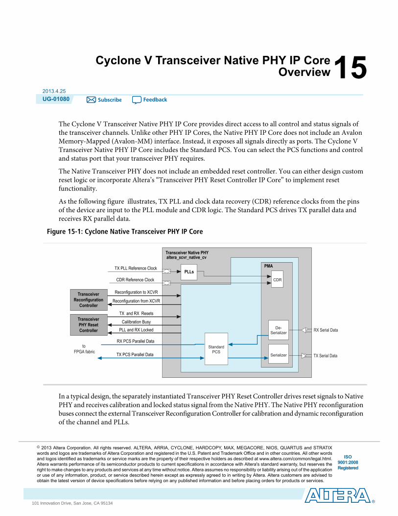
15Cyclone V Transceiver Native PHY IP CoreOverview
2013.4.25UG-01080 Subscribe Feedback
The Cyclone V Transceiver Native PHY IP Core provides direct access to all control and status signals ofthe transceiver channels. Unlike other PHY IP Cores, the Native PHY IP Core does not include an AvalonMemory-Mapped (Avalon-MM) interface. Instead, it exposes all signals directly as ports. The Cyclone VTransceiver Native PHY IP Core includes the Standard PCS. You can select the PCS functions and controland status port that your transceiver PHY requires.
The Native Transceiver PHY does not include an embedded reset controller. You can either design customreset logic or incorporate Altera’s “Transceiver PHY Reset Controller IP Core” to implement resetfunctionality.
As the following figure illustrates, TX PLL and clock data recovery (CDR) reference clocks from the pinsof the device are input to the PLL module and CDR logic. The Standard PCS drives TX parallel data andreceives RX parallel data.
Figure 15-1: Cyclone Native Transceiver PHY IP Core
PLLsPMA
altera_xcvr_native_cvTransceiver Native PHY
RX PCS Parallel Data
TX PCS Parallel Data
CDR Reference Clock
TX PLL Reference Clock
CDR
RX Serial Data
toFPGA fabric
TransceiverReconfiguration
Controller
Reconfiguration to XCVR
Reconfiguration from XCVR
TX and RX Resets
Calilbration BusyPLL and RX Locked
TransceiverPHY ResetController
TX Serial DataSerializer
De-Serializer
StandardPCS
In a typical design, the separately instantiated Transceiver PHYReset Controller drives reset signals toNativePHY and receives calibration and locked status signal from theNative PHY. TheNative PHY reconfigurationbuses connect the external TransceiverReconfigurationController for calibration anddynamic reconfigurationof the channel and PLLs.
ISO9001:2008Registered
© 2013 Altera Corporation. All rights reserved. ALTERA, ARRIA, CYCLONE, HARDCOPY, MAX, MEGACORE, NIOS, QUARTUS and STRATIXwords and logos are trademarks of Altera Corporation and registered in the U.S. Patent and Trademark Office and in other countries. All other wordsand logos identified as trademarks or service marks are the property of their respective holders as described at www.altera.com/common/legal.html.Altera warrants performance of its semiconductor products to current specifications in accordance with Altera's standard warranty, but reserves theright to make changes to any products and services at any time without notice. Altera assumes no responsibility or liability arising out of the applicationor use of any information, product, or service described herein except as expressly agreed to in writing by Altera. Altera customers are advised toobtain the latest version of device specifications before relying on any published information and before placing orders for products or services.
www.altera.com
101 Innovation Drive, San Jose, CA 95134

You specify the initial configuration when you parameterize the IP core. The Transceiver Native PHY IPCore connects to the “Transceiver Reconfiguration Controller IP Core” to dynamically change referenceclocks, PLL connectivity, and the channel configurations at runtime.
Related InformationTransceiver PHY Reset Controller IP Core on page 17-1
Transceiver Reconfiguration Controller IP Core Overview on page 16-1
Cyclone Device Family SupportIP cores provide either final or preliminary support for target Altera device families. These terms have thefollowing definitions:
• Final support—Verified with final timing models for this device.• Preliminary support—Verified with preliminary timing models for this device.
Table 15-1: Device Family Support
SupportDevice Family
PreliminaryCyclone V devices
No supportOther device families
Cyclone V Native PHY Performance and Resource UtilizationBecause the Standard PCS and PMA are implemented in hard logic, the Cyclone V Native PHY IP Corerequires minimal resources.
Parameterizing the Cyclone V Native PHYComplete the following steps to configure the Cyclone V Native PHY IP Core in the MegaWizard Plug-InManager:
1. For Which device family will you be using?, select Cyclone V from the list.2. Click Installed Plug-Ins > Interfaces > Transceiver PHY > Cyclone V Native PHY v12.1 .3. Use the tabs on the MegaWizard Plug-In Manager to select the options required for the protocol.4. Click Finish to generate your customized Cyclone V Native PHY IP Core.
The Cyclone V Transceiver Native PHY provides presets for CPRI, GIGE, and the Low LatencyStandard PCS. The presets specify the parameters required to the protocol specified.
Note:
General ParametersThis section lists the parameters available on the General Options tab.
Cyclone V Transceiver Native PHY IP Core OverviewAltera Corporation
Feedback
UG-01080Cyclone Device Family Support15-2 2013.4.25
Table 15-2: General and Datapath Options
DescriptionRangeName
Specifies the speed grade.fastestDevice speed grade
Allows you to specify the message level, as follows:
• error: Quartus II checker will not create an instance withinvalid parameters. You must change incompatibleparameter selections to proceed.
• warning: Quartus II checker will allow instance creationwith invalid parameters, but the instancewill not compilesuccessfully.
error
warningMessage level for ruleviolations
Datapath Options
When you turn this option On, the core includes the TXdatapath.
On/OffEnable TX datapath
When you turn this option On, the core includes the RXdatapath.
On/OffEnable RX datapath
The Cyclone V Native PHY only supports the Standarddatapath.
StandardInitial PCS datapathselection
Specifies the total number of data channels in each direction.1-36Number of data channels
In Non–bonded mode, each channel is assigned a PLL.During Quartus II compilation, the Fitter merges all PLLsthat meet merging requirements into a single PLL.
Select ×N to use the same clock source for up to 6 channelsin a single transceiver bank or the same clock source for allthe transceivers on one side of the device. ×Nbonding resultsin reduced clock skew. You must use contiguous channelswhen you select ×N bonding.
For more information about the clock architecture ofbonding, refer to “Transmitter Clock Network” inTransceiver Clocking inCycloneV Devices in volume 2 of theCyclone V Device Handbook.
Non–bonded
×N
Bonding mode
Altera CorporationCyclone V Transceiver Native PHY IP Core Overview
Feedback
15-3General ParametersUG-010802013.4.25
DescriptionRangeName
When you turn this option On, the data interface providesonly the relevant interface to the FPGA fabric for the selectedconfiguration. You can only use this option for staticconfigurations.
When you turn this option Off, the data interface providesthe full physical interface to the fabric. Select this option ifyou plan to use dynamic reconfiguration that includeschanging the interface to the FPGA fabric.
Refer to “Active Bits for Each Fabric Interface Width” forguidance.
On/OffEnable simplified datainterface
Related InformationTransceiver Clocking in Cyclone V Devices
PMA ParametersThis section describes the options available for the PMA.
For more information about the PMA, refer to the PMAArchitecture section in the Transceiver Architecturein Cyclone V Devices. Some parameters have ranges where the value is specified as Device Dependent. Forsuch parameters, the possible range of frequencies and bandwidths depends on the device, speed grade, andother design characteristics. Refer to Device Datasheet for Cyclone V Devices for specific data for CycloneV devices.
Table 15-3: PMA Options
DescriptionRangeParameter
Specifies the data rate. Themaximumdata rate is 12.5Gbps.Device DependentData rate
Specifies the value of the divider available in the transceiverchannels to divide the input clock to generate the correctfrequencies for the parallel and serial clocks. This divisordivides the fast clock from the PLL in nonbondedconfigurations.
1, 2, 4, 8TX local clock divisionfactor
Shows the base data rate of the clock input to the TXPLL.The PLL base data rate is computed from the TX localclock division factor multiplied by the data rate.
Select a PLL base data rate that minimizes the number ofPLLs required to generate all the clocks for data transmission.By selecting an appropriate PLL base data rate, you canchange data rates by changing the TX local clock divisionfactor used by the clock generation block.
Device DependentPLL base data rate
Cyclone V Transceiver Native PHY IP Core OverviewAltera Corporation
Feedback
UG-01080PMA Parameters15-4 2013.4.25

Related InformationTransceiver Architecture in Cyclone V Devices
Device Datasheet for Cyclone V Devices
TX PMA ParametersFor more information about PLLs in Cyclone V devices, refer to the Cyclone V PLLs section in ClockNetworks and PLLs in Cyclone V Devices.
Note:
Table 15-4: TX PMA Parameters
DescriptionRangeParameter
When you turn this option On, you can dynamicallyreconfigure the PLL. This option is also required to simulateTX PLL reconfiguration. If you turn this option On, theQuartus II Fitter prevents PLLmerging by default; however,you can specify merging using the FORCE_MERGE_PLLQSF assignments.
On/OffEnable TX PLL dynamicreconfiguration
When you turn this option On, the Native PHY does notinclude TX PLLs. Instead, the Native PHY includes a inputclock port for connection to the fast clock from an externalPLL, ext_pll_clk[<p>-1:0] that you can connect toexternal PLLs. Use feature when need to perform TX PLLswitching between fractional PLL and a CMU PLL.
On/OffUse external TX PLL
Specifies the number of TXPLLs required.More than 1 PLLis typically required if your design reconfigures channels torun at multiple frequencies.
1–4Number of TX PLLs
Specifies the index of the TX PLL used in the initialconfiguration.
0–3Main TX PLL logical index
Specifies the total number of reference clocks that are usedby all of the PLLs.
1–5Number of TX PLLreference clocks
Related InformationClock Networks and PLLs in Cyclone V Devices
TX PLL<n>This section allows you to define multiple TX PLLs for your Native PHY. The Native PHY GUI provides aseparate tab for each TX PLL.
Table 15-5: TX PLL Parameters
DescriptionRangeParameter
This is the only PLL type available.CMUPLL type
Altera CorporationCyclone V Transceiver Native PHY IP Core Overview
Feedback
15-5TX PMA ParametersUG-010802013.4.25

DescriptionRangeParameter
Shows the base data rate of the clock input to the TXPLL.The PLL base data rate is computed from the TX localclock division factor multiplied by the Data rate.
Select a PLL base data rate that minimizes the number ofPLLs required to generate all the clocks for data transmission.By selecting an appropriate PLL base data rate, you canchange data rates by changing the TX local clock divisionfactor used by the clock generation block.
Device DependentPLL base data rate
Specifies the frequency of the reference clock for the Selectedreference clock source index you specify. You can define asingle frequency for each PLL. You can use the TransceiverReconfiguration Controller to dynamically change thereference clock input to the PLL.
Note that the list of frequencies updates dynamically whenyou change the Data rate. The Input clock frequency dropdown menu is populated with all valid frequencies derivedas a function of the Data rate and Base data rate.
Device DependentReference clock frequency
You can define up to 5 reference clock sources for the PLLsin your core. The Reference clock frequency selected forindex 0, is assigned to TX PLL<0>. The Reference clockfrequency selected for index 1, is assigned to TX PLL<1>,and so on.
0–4Selected reference clocksource
Specifies nonbonded (separate) or shared PLLs for the clocknetwork.
non bonded ×NSelected clock network
RX PMA ParametersThis section describes the RX PMA options you can specify.
For more information about the CDR circuitry, refer to the Receiver PMA Datapath section in theTransceiver Architecture in Cyclone V Devices Cyclone V Devices.
Note:
Table 15-6: RX PMA Parameters
DescriptionRangeParameter
When you turn this optionOn, you can dynamically changethe data rate of the CDR circuit.
On/OffEnable CDR dynamicreconfiguration
Specifies the number of reference clocks for the CDRs.1–5Number of CDR referenceclocks
Specifies the index of the selected CDR reference clock.0–4Selected CDR referenceclock
Cyclone V Transceiver Native PHY IP Core OverviewAltera Corporation
Feedback
UG-01080RX PMA Parameters15-6 2013.4.25

DescriptionRangeParameter
Specifies the frequency of the clock input to the CDR.Device DependentSelected CDR referenceclock frequency
Specifies themaximumPPMdifference theCDRcan toleratebetween the input reference clock and the recovered clock.
Device DependentPPM detector threshold
When you turn this option On, the RX parallel clock whichis recovered from the serial received data is an output of thePMA.
On/OffEnable rx_pma_clkout port
When you turn this option On, the rx_is_lockedtodata port is an output of the PMA.
On/OffEnable rx_is_lockedtodataport
Whenyou turn this optionOn, therx_is_lockedtorefport is an output of the PMA.
On/OffEnable rx_is_lockedtorefport
When you turn this option On, the rx_set_lockedtdata and rx_set_lockedtoref ports areoutputs of the PMA.
On/OffEnable rx_set_lockedtodataand rx_set_locktoref ports
When you turn this option On, the rx_pma_bitslip isan input to the core. The deserializer slips one clock edgeeach time this signal is asserted. You can use this feature tominimize uncertainty in the serialization process as requiredby protocols that require a datapath with deterministiclatency such as CPRI.
On/OffEnable rx_pma_bitslip_port
When you turn this option On, the rx_seriallpbkenis an input to the core. When your drive a 1 on this inputport, the PMA operates in serial loopback mode with TXdata looped back to the RX channel.
On/OffEnable rx_seriallpbkenport
Related InformationTransceiver Architecture in Cyclone V Devices Cyclone V Devices
Standard PCS ParametersThis section illustrates the complete datapath and clocking for the Standard PCS and defines the parametersavailable to enable or disable the individual blocks in the Standard PCS.
Figure 15-2: The Standard PCS Datapath
Formore information about the Standard PCS, refer to thePCSArchitecture section in theTransceiverArchitecture in Cyclone V Devices.
Note:
The following table describes the general and datapath options for the Standard PCS.
Altera CorporationCyclone V Transceiver Native PHY IP Core Overview
Feedback
15-7Standard PCS ParametersUG-010802013.4.25
Table 15-7: General and Datapath Parameters
DescriptionRangeParameter
Specifies the protocol that you intend to implement withthe Native PHY. The protocol mode selected guides theMegaWizard in identifying legal settings for the StandardPCS datapath.
Use the following guidelines to select a protocol mode:
• basic–select thismode forwhennone of the other optionsare appropriate. You should also select this mode toenable diagnostics, such as loopback.
• cpri–select this mode if you intend to implement CPRIor another protocol that requires deterministic latency.Altera recommends that you select the appropriate CPRIpreset for the CPRI protocol.
• gige–select this mode if you intend to implement eitherthe 1.25 Gbps or 2.5 Gbps Ethernet protocol. Alterarecommends that you select the appropriate preset forthe Ethernet protocol.
basic
cpri
gige
Standard PCS protocolmode
Specifies the width of the datapath that connects the FPGAfabric to the PMA. The transceiver interface width dependsupon whether you enable 8B/10B. To simplify connectivitybetween the FPGA fabric and PMA, the bus bits used arenot contiguous for 16 and 32bit buses. Refer to Active Bitsfor Each Fabric Interface Width for the bits used.
8, 10,16, 20Standard PCS/PMAinterface width
Shows the FPGA fabric to TX PCS interface width which iscalculated from the Standard PCS/PMA interface width .
8, 10,16, 20, 32,40
FPGA fabric/Standard TXPCS interface width
Shows the FPGA fabric to RX PCS interface width which iscalculated from the Standard PCS/PMA interface width .
8, 10,16, 20, 32,40
FPGA fabric/Standard RXPCS interface width
When you turn this option On, all PCS functions aredisabled except for the phase compensation FIFO, byteserializer and byte deserializer. This option creates the lowestlatencyNative PHY that allows dynamic reconfigure betweenmultiple PCS datapaths.
On/OffEnable Standard PCS lowlatency mode
Phase Compensation FIFOThe phase compensation FIFO assures clean data transfer to and from the FPGA fabric by compensatingfor the clock phase difference between the low speed parallel clock and FPGA fabric interface clock.
For more information refer to the Receiver Phase Compensation FIFO and Transmitter PhaseCompensation FIFO sections in the Transceiver Architecture in Cyclone V Devices.
Note:
Cyclone V Transceiver Native PHY IP Core OverviewAltera Corporation
Feedback
UG-01080Phase Compensation FIFO15-8 2013.4.25

Table 15-8: Phase Compensation FIFO Parameters
DescriptionRangeParameter
The following 2 modes are possible:
• low_latency: This mode adds 3–4 cycles of latency tothe TX datapath.
• register_fifo: In this mode the FIFO is replaced byregisters to reduce the latency through the PCS. Usethis mode for protocols that require deterministiclatency, such as CPRI.
low_latencyregister_fifo
TX FIFO mode
The following 2 modes are possible:
• low_latency: This mode adds 2–3 cycles of latency tothe TX datapath.
• register_fifo: In this mode the FIFO is replaced byregisters to reduce the latency through the PCS. Usethis mode for protocols that require deterministiclatency, such as CPRI.
low_latencyregister_fifo
RX FIFO mode
When you turn this option On, the TX Phasecompensation FIFO outputs a FIFO full status flag.
On/OffEnable tx_std_pcfifo_full port
When you turn this option On, the TX Phasecompensation FIFO outputs a FIFO empty status flag.
On/OffEnable tx_std_pcfifo_emptyport
When you turn this option On, the RX Phasecompensation FIFO outputs a FIFO full status flag.
On/OffEnable rx_std_pcfifo_full port
When you turn this option On, the RX Phasecompensation FIFO outputs a FIFO empty status flag.
On/OffEnable rx_std_pcfifo_emptyport
When you turn this option On, the rate match FIFOoutputs a FIFO empty status flag. The rate match FIFOcompensates for small clock frequency differencesbetween the upstream transmitter and the local receiverclocks by inserting or removing skip (SKP) symbols orordered sets from the interpacket gap (IPG) or idle stream.
On/OffEnable rx_std_rmfifo_emptyport
When you turn this option On, the rate match FIFOoutputs a FIFO full status flag.
On/OffEnable rx_std_rmfifo_full port
Related InformationTransceiver Architecture in Cyclone V Devices
Byte Ordering Block ParametersTheRXbyte ordering block realigns the data coming from the byte deserializer. This block is necessarywhenthe PCS to FPGA fabric interface width is greater than the PCS datapath.
Altera CorporationCyclone V Transceiver Native PHY IP Core Overview
Feedback
15-9Byte Ordering Block ParametersUG-010802013.4.25

Because the timing of the RX PCS reset logic is indeterminate, the byte ordering at the output of the bytedeserializer may or may not match the original byte ordering of the transmitted data.
For more information refer to the Byte Ordering section in theTransceiver Architecture in Cyclone VDevices.
Note:
Table 15-9: Byte Ordering Block Parameters
DescriptionRangeParameter
When you turn this option On, the PCS includes thebyte ordering block.
On/OffEnable RX byte ordering
Specifies the control mode for the byte ordering block.The following modes are available:
• Manual: Allows you to control the byte orderingblock
• Auto: The word aligner automatically controls thebyte ordering block once word alignment isachieved.
manual
auto
Byte ordering control mode
Shows width of the pattern that you must specify. Thiswidth depends upon the PCSwidth andwhether or not8B/10B encoding is used as follows:
8–10Byte ordering pattern width Pad Pattern
8 bits
10 bits
9 bits
8B/10B
No
No
Yes
Width
8, 16,32
10,20,40
8,16,32
Specifies the number of symbols the word alignershould search for. When the PMA is 16 or 20 bits wide,the byte ordering block can optionally search for 1 or2 symbols.
1–2Byte ordering symbol count
Specifies the search pattern for the byte ordering block.User-specified 8-10bit pattern
Byte order pattern (hex)
Cyclone V Transceiver Native PHY IP Core OverviewAltera Corporation
Feedback
UG-01080Byte Ordering Block Parameters15-10 2013.4.25

DescriptionRangeParameter
Specifies the pad pattern that is inserted by the byteordering block. This value is inserted when the byteorder pattern is recognized.
The byte ordering pattern should occupy the leastsignificant byte (LSB) of the parallel TX data. If the byteordering block identifies the programmedbyte orderingpattern in the most significant byte (MSB) of thebyte-deserialized data, it inserts the appropriate numberof user-specified pad bytes to push the byte orderingpattern to the LSB position, restoring proper byteordering.
User–specified 8-10bit pattern
Byte order pad value (hex)
Enables the optional rx_std_byte_order_enacontrol input port. When this signal is asserted, thebyte ordering block initiates a byte ordering operationif the Byte ordering control mode is set to manual.Once byte ordering has occurred, you must deassertand reassert this signal to perform another byteordering operation. This signal is an synchronous inputsignal; however, it must be asserted for at least 1 cycleof rx_std_clkout.
On/OffEnable rx_std_byteorder_enaport
Enables the optional rx_std_byteorder_flagstatus output port. When asserted, indicates that thebyte ordering block has performed a byte orderoperation. This signal is asserted on the clock cycle inwhich byte ordering occurred. This signal issynchronous to the rx_std_clkout clock.
On/OffEnable rx_std_byteorder_flagport
Related InformationTransceiver Architecture in Cyclone V Devices
Byte Serializer and DeserializerThe byte serializer and deserializer allow the PCS to operate at twice the data width of the PMA serializer.This feature allows the PCS to run at a lower frequency and accommodate a wider range of FPGA interfacewidths.
For more information refer to the Byte Serializer and Byte Deserializer sections in the TransceiverArchitecture in Cyclone V Devices.
Note:
Altera CorporationCyclone V Transceiver Native PHY IP Core Overview
Feedback
15-11Byte Serializer and DeserializerUG-010802013.4.25

Table 15-10: Byte Serializer and Deserializer Parameters
DescriptionRangeParameter
When you turn this option On, the PCS includes a TXbyte serializer which allows the PCS to run at a lowerclock frequency to accommodate a wider range of FPGAinterface widths.
On/OffEnable TX byte serializer
When you turn this option On, the PCS includes an RXbyte deserializer which allows the PCS to run at a lowerclock frequency to accommodate a wider range of FPGAinterface widths.
On/OffEnable RX byte deserializer
Related InformationTransceiver Architecture in Cyclone V Devices
8B/10BThe 8B/10B encoder generates 10-bit code groups from the 8-bit data and 1-bit control identifier. The 8B/10Bdecoder decodes the data into an 8-bit data and 1-bit control identifier.
In 8-bit width mode, the 8B/10B encoder translates the 8-bit data to a 10-bit code group (control word ordata word) with proper disparity.
For more information refer to the 8B/10B Encoder and 8B/10B Decoder sections in the TransceiverArchitecture in Cyclone V Devices.
Note:
Table 15-11: 8B/10B Encoder and Decoder Parameters
DescriptionRangeParameter
When you turn this optionOn, the PCS includes the 8B/10Bencoder.
On/OffEnable TX 8B/10B encoder
When you turn this option On, the PCS includes disparitycontrol for the 8B/10B encoder. You force the disparity ofthe 8B/10B encoder using the tx_forcedisp and tx_dispval control signal.
On/OffEnableTX8B/10Bdisparitycontrol
When you turn this optionOn, the PCS includes the 8B/10Bdecoder.
On/OffEnable RX 8B/10B decoder
Related InformationTransceiver Architecture in Cyclone V Devices
Rate Match FIFOThe rate match FIFO compensates for the very small frequency differences between the local system clockand the RX recovered clock.
For more information refer to the Rate Match FIFO sections in the Transceiver Architecture in Cyclone VDevices.
Cyclone V Transceiver Native PHY IP Core OverviewAltera Corporation
Feedback
UG-010808B/10B15-12 2013.4.25
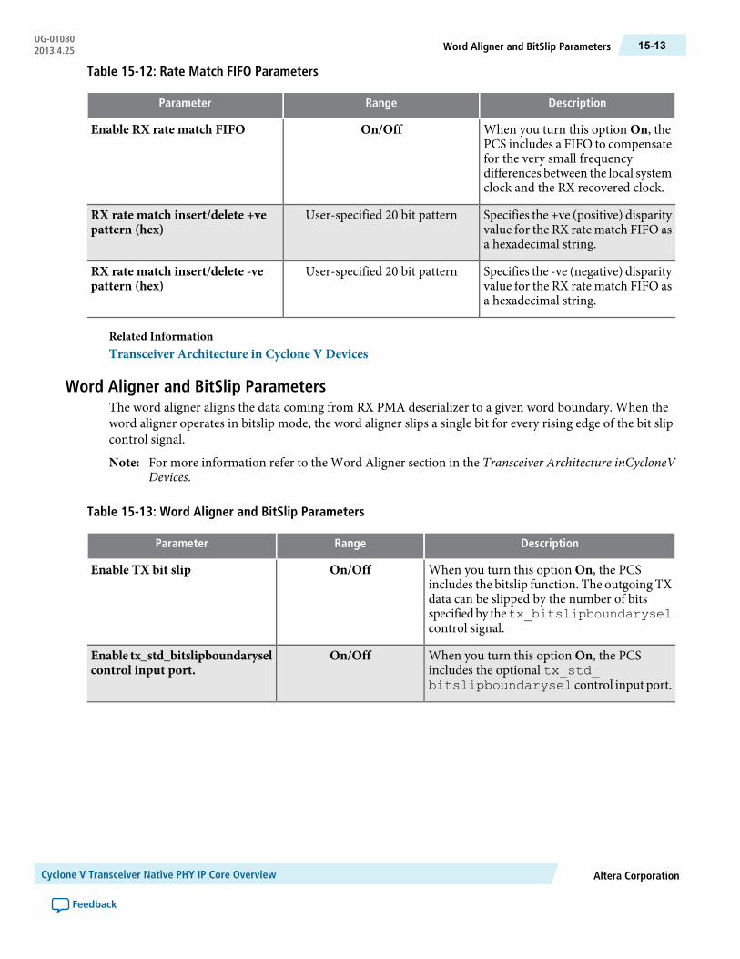
Table 15-12: Rate Match FIFO Parameters
DescriptionRangeParameter
When you turn this option On, thePCS includes a FIFO to compensatefor the very small frequencydifferences between the local systemclock and the RX recovered clock.
On/OffEnable RX rate match FIFO
Specifies the +ve (positive) disparityvalue for the RX rate match FIFO asa hexadecimal string.
User-specified 20 bit patternRX rate match insert/delete +vepattern (hex)
Specifies the -ve (negative) disparityvalue for the RX rate match FIFO asa hexadecimal string.
User-specified 20 bit patternRX rate match insert/delete -vepattern (hex)
Related InformationTransceiver Architecture in Cyclone V Devices
Word Aligner and BitSlip ParametersThe word aligner aligns the data coming from RX PMA deserializer to a given word boundary. When theword aligner operates in bitslip mode, the word aligner slips a single bit for every rising edge of the bit slipcontrol signal.
For more information refer to the Word Aligner section in the Transceiver Architecture inCycloneVDevices.
Note:
Table 15-13: Word Aligner and BitSlip Parameters
DescriptionRangeParameter
When you turn this option On, the PCSincludes the bitslip function. The outgoing TXdata can be slipped by the number of bitsspecifiedby thetx_bitslipboundaryselcontrol signal.
On/OffEnable TX bit slip
When you turn this option On, the PCSincludes the optional tx_std_bitslipboundarysel control input port.
On/OffEnable tx_std_bitslipboundaryselcontrol input port.
Altera CorporationCyclone V Transceiver Native PHY IP Core Overview
Feedback
15-13Word Aligner and BitSlip ParametersUG-010802013.4.25

DescriptionRangeParameter
Specifies one of the following 3 modes for theword aligner:
• Bit_slip: You can use bit slip mode to shiftthe word boundary. For every rising edgeof the rx_bitslip signal, the wordboundary is shifted by 1 bit. Each bitslipremoves the earliest received bit from thereceived data
• Sync_sm: In synchronous state machinemode, a programmable state machinecontrols word alignment. You can only usethis mode with 8B/10B encoding. The datawidth at the word aligner can be 10 or 20bits
• Manual: Thismode enablesword alignmentby asserting the rx_std_wa_pattern.This is an edge sensitive signal.
bit_slip
sync_sm
manual
RX word aligner mode
Specifies the length of the pattern the wordaligner uses for alignment. The pattern isspecified in LSBtoMSB order.
7,8,10,16
20, 32,40
RX word aligner pattern length
Specifies the word aligner pattern in hex.User-specifiedRX word aligner pattern (hex)
Specifies the number of valid word alignmentpatterns that must be received before the wordaligner achieves synchronization lock. Thedefault is 3.
1–256Number of word alignmentpatterns to achieve sync
Specifies the number of invalid data codes ordisparity errors that must be received beforethe word aligner loses synchronization. Thedefault is 3.
1–256Number of invalid words to losesync
Specifies the number of valid data codes thatmust be received to decrement the errorcounter. If the word aligner receives enoughvalid data codes to decrement the error countto 0, the word aligner returns tosynchronization lock.
1–256Number of valid data words todecrement error count
Specifies the maximum number of contiguous0s or 1s in the data stream before the wordaligner reports a run length violation.
0–63Run length detector word count
Enables the optional rx_std_wa_patternalign control input port.
On/OffEnable rx_std_wa_patternalignport
Enables the optional rx_std_wa_a1a2size control input port.
On/OffEnable rx_std_wa_a1a2size port
Cyclone V Transceiver Native PHY IP Core OverviewAltera Corporation
Feedback
UG-01080Word Aligner and BitSlip Parameters15-14 2013.4.25
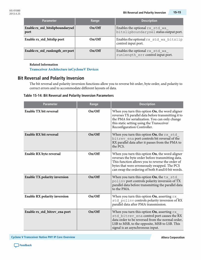
DescriptionRangeParameter
Enables the optional rx_std_wa_bitslipboundarysel status output port.
On/OffEnable rx_std_bitslipboundaryselport
Enables the optionalrx_std_wa_bitslipcontrol input port.
On/OffEnable rx_std_bitslip port
Enables the optional rx_std_wa_runlength_err control input port.
On/OffEnable rx_std_runlength_errport
Related InformationTransceiver Architecture inCycloneV Devices
Bit Reversal and Polarity InversionThe bit reversal and polarity inversion functions allow you to reverse bit order, byte order, and polarity tocorrect errors and to accommodate different layouts of data.
Table 15-14: Bit Reversal and Polarity Inversion Parameters
DescriptionRangeParameter
When you turn this option On, the word alignerreverses TX parallel data before transmitting it tothe PMA for serialization. You can only changethis static setting using the TransceiverReconfiguration Controller.
On/OffEnable TX bit reversal
When you turn this option On, the rx_std_bitrev_ena port controls bit reversal of theRX parallel data after it passes from the PMA tothe PCS.
On/OffEnable RX bit reversal
When you turn this option On, the word alignerreverses the byte order before transmitting data.This function allows you to reverse the order ofbytes that were erroneously swapped. The PCScan swap the ordering of both 8 and10 bit words.
On/OffEnable RX byte reversal
When you turn this option On, the tx_std_polinv port controls polarity inversion of TXparallel data before transmitting the parallel datato the PMA.
On/OffEnable TX polarity inversion
When you turn this option On, asserting rx_std_polinv controls polarity inversion of RXparallel data after PMA transmission.
On/OffEnable RX polarity inversion
When you turn this option On, asserting rx_std_bitrev_ena control port causes the RXdata order to be reversed from the normal order,LSB to MSB, to the opposite, MSB to LSB. Thissignal is an asynchronous input.
On/OffEnable rx_std_bitrev_ena port
Altera CorporationCyclone V Transceiver Native PHY IP Core Overview
Feedback
15-15Bit Reversal and Polarity InversionUG-010802013.4.25

DescriptionRangeParameter
When you turn this option On, asserting rx_std_byterev_ena input control port swapsthe order of the individual 8 or 10bit wordsreceived from the PMA.
On/OffEnable rx_std_byterev_ena port
When you turn this option On, the tx_std_polinv input is enabled. You canuse this controlport to swap the positive and negative signals ofa serial differential link if they were erroneouslyswapped during board layout.
On/OffEnable tx_std_polinv port
When you turn this option On, the rx_std_polinv input is enabled. You canuse this controlport to swap the positive and negative signals ofa serial differential link if they were erroneouslyswapped during board layout.
On/OffEnable rx_std_polinv port
When you turn this option On, the tx_std_elecidle input port is enabled. When thissignal is asserted, it forces the transmitter toelectrical idle.
On/OffEnable tx_std_elecidle port
When you turn this option On, the optional rx_std_signaldetect output port is enabled.This signal is required for the PCI Expressprotocol. If enabled, the signal threshold detectioncircuitry senses whether the signal level presentat the RX input buffer is above the signal detectthreshold voltage that you specified.
On/OffEnable rx_std_signaldetect port
InterfacesThe Native PHY includes several interfaces that are common to all parameterizations.
The Native PHY allows you to enable ports, even for disabled blocks to facilitate dynamic reconfiguration.
The Native PHY uses the following prefixes for port names:
• Standard PCS ports—tx_std, rx_std
The port descriptions use the following variables to represent parameters:
• <n>—The number of lanes• <p>—The number of PLLs• <r>—the number of CDR references clocks selected
Common Interface PortsCommon interface consists of reset, clock signals, serial interface ports, control and status ports, paralleldata ports, and reconfig interface ports.
Cyclone V Transceiver Native PHY IP Core OverviewAltera Corporation
Feedback
UG-01080Interfaces15-16 2013.4.25

Figure 15-3: Common Interface Ports
tx_pll_refclk[<r>-1:0]tx_pma_clkout[<n>-1:0]rx_pma_clkout[<n>-1:0]rx_clklow[<n>-1:0]rx_fref[<n>-1:0]rx_cdr_refclk[<r>-1:0]
Clock Input& Output Signals
rx_seriallpbken[<n>-1:0]rx_setlocktodata[<n>-1:0]rx_setlocktoref[<n>-1:0]
pll_locked[<p>-1:0]rx_is_lockedtodata[<n>-1:0]rx_is_lockedtoref[<n>-1:0]
rx_clkslip[<n>-1:0]
Control &Status Portspll_powerdown[<p>-1:0]
tx_analogreset[<n>-1:0]tx_digitalreset[<n>-1:0]rx_analogreset[<n>-1:0]rx_digitalreset[<n>-1:0]
Resets
tx_parallel_data[<n>43-1:0]rx_parallel_data[<n>64-1:0]
ParallelData Ports
tx_serial_data[<n>-1:0]rx_serial_data[<n>-1:0]
TX & RXSerial Ports
reconfig_to_xcvr [(<n>70-1):0]reconfig_from_xcvr [(<n>46-1):0]
tx_cal_busy[<n>-1:0]rx_cal_busy[<n>-1:0]
ReconfigurationInterface Ports
Native PHY Common Interfaces
Table 15-15: Native PHY Common Interfaces
DescriptionDirectionName
Clock Inputs and Output Signals
The reference clock input to the TX PLL.Inputtx_pll_refclk[<r>-1:0]
RX parallel clock (recovered clock) output fromPMA
Outputrx_pma_clkout[<n>-1:0]
The RX parallel recovered clock input to the phasefrequency detector (PFD).When operatingCDR inmanual lock mode, you can use this clock as aninput with rx_fref to an external PPM detector.
Outputrx_clklow[<n>-1:0]
TheRX local reference lock input to the PFD.Whenoperating CDR in manual lock mode, you can usethis clock with rx_clklow as an input to anexternal PPM detector.
Outputrx_fref[<n>-1:0]
Input reference clock for the RX PFD circuit.Inputrx_cdr_refclk[<n>-1:0]
Resets
When asserted, resets the TXPLL. Active high, edgesensitive reset signal. By default, the Cyclone NativeTransceiver PHY IP Core create a separate pll_powerdown signal for each logical PLL. However,the Fittermaymerge the PLLs if they are in the sametransceiver bank. PLLs can only be merged if theirpll_powerdown signals are driven from the samesource. If the PLLs are in separate transceiver banks,you can choose to drive the pll_powerdownsignals separately.
Inputpll_powerdown[<p>-1:0]
Altera CorporationCyclone V Transceiver Native PHY IP Core Overview
Feedback
15-17Common Interface PortsUG-010802013.4.25

DescriptionDirectionName
When asserted, resets for TX PMA, TX clockgeneration block, and serializer. Active high, edgesensitive reset signal.
Inputtx_analogreset[<n>-1:0]
When asserted, resets the digital components of theTX datapath. Active high, edge sensitive,asynchronous reset signal. If your design includesbonded TX PCS channels, refer to TimingConstraints for Reset Signals when Using BondedPCS Channels for a SDC constraint you mustinclude in your design.
Inputtx_digitalreset[<n>-1:0]
When asserted, resets the RX CDR, deserializer.Active high, edge sensitive, asynchronous resetsignal.
Inputrx_analogreset[<n>-1:0]
When asserted, resets the digital components of theRX datapath. Active high, edge sensitive,asynchronous reset signal.
Inputrx_digitalreset[<n>-1:0]
Parallel data ports
PCS TX parallel data. Used when you enable theStandard datapath.
Inputtx_parallel_data[43:0]
PCS RX parallel data. Used when you enable theStandard datapath.
Outputrx_parallel_data[63:0]
TX and RX serial ports
TX differential serial output data.Outputtx_serial_data[<n>-1:0]
RX differential serial output data.Inputrx_serial_data[<n>-1:0]
Control and Status ports
When asserted, the transceiver enters serial loopbackmode. Loopback drives serial TX data to the RXinterface.
Inputrx_seriallpbken[<n>-1:0]
When asserted, programs the RX CDR to manuallock to data mode in which you control the resetsequence using the rx_set_locktoref andrx_set_locktodata. Refer to “TransceiverReset Sequence” in Transceiver Reset Control inCyclone V Devices for more information aboutmanual control of the reset sequence.
Inputrx_set_locktodata[<n>-1:0]
Cyclone V Transceiver Native PHY IP Core OverviewAltera Corporation
Feedback
UG-01080Common Interface Ports15-18 2013.4.25
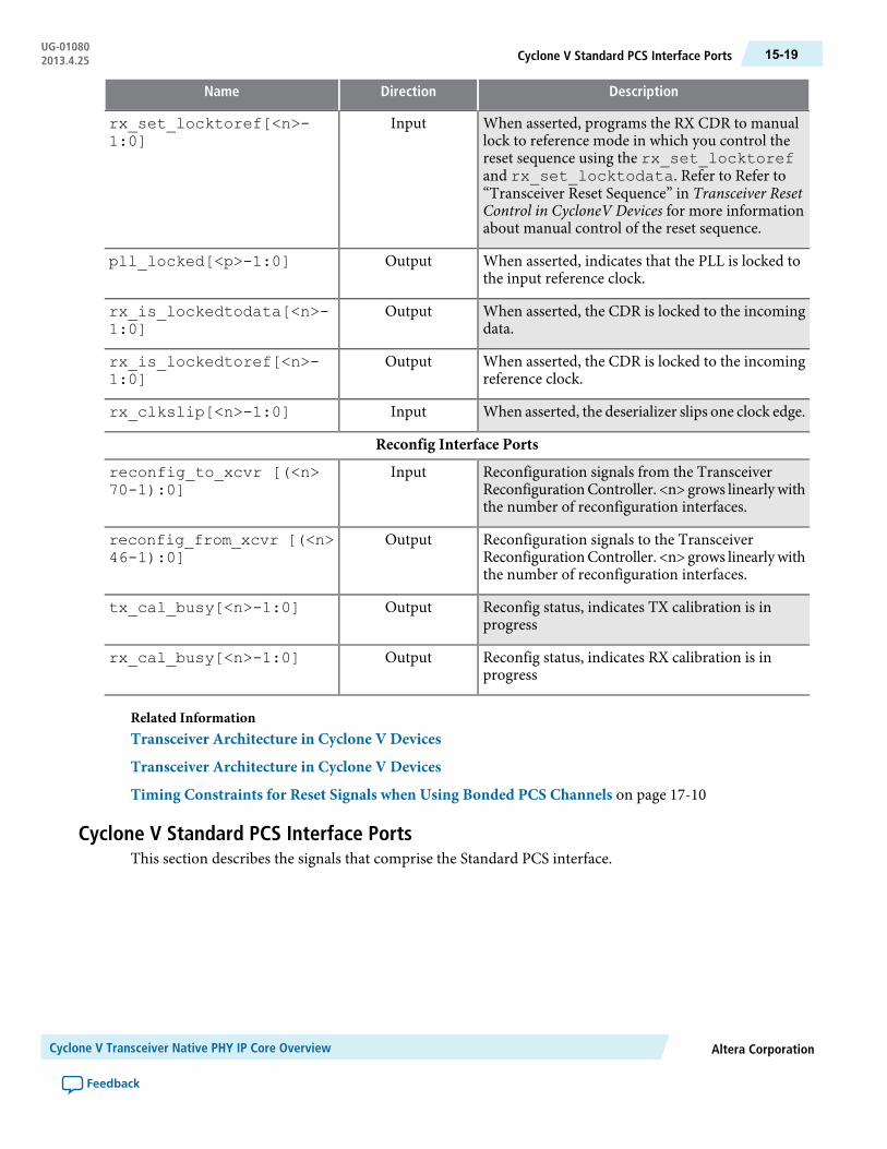
DescriptionDirectionName
When asserted, programs the RX CDR to manuallock to reference mode in which you control thereset sequence using the rx_set_locktorefand rx_set_locktodata. Refer to Refer to“Transceiver Reset Sequence” in Transceiver ResetControl in CycloneV Devices for more informationabout manual control of the reset sequence.
Inputrx_set_locktoref[<n>-1:0]
When asserted, indicates that the PLL is locked tothe input reference clock.
Outputpll_locked[<p>-1:0]
When asserted, the CDR is locked to the incomingdata.
Outputrx_is_lockedtodata[<n>-1:0]
When asserted, the CDR is locked to the incomingreference clock.
Outputrx_is_lockedtoref[<n>-1:0]
When asserted, the deserializer slips one clock edge.Inputrx_clkslip[<n>-1:0]
Reconfig Interface Ports
Reconfiguration signals from the TransceiverReconfigurationController. <n> grows linearlywiththe number of reconfiguration interfaces.
Inputreconfig_to_xcvr [(<n>70-1):0]
Reconfiguration signals to the TransceiverReconfigurationController. <n> grows linearlywiththe number of reconfiguration interfaces.
Outputreconfig_from_xcvr [(<n>46-1):0]
Reconfig status, indicates TX calibration is inprogress
Outputtx_cal_busy[<n>-1:0]
Reconfig status, indicates RX calibration is inprogress
Outputrx_cal_busy[<n>-1:0]
Related InformationTransceiver Architecture in Cyclone V Devices
Transceiver Architecture in Cyclone V Devices
Timing Constraints for Reset Signals when Using Bonded PCS Channels on page 17-10
Cyclone V Standard PCS Interface PortsThis section describes the signals that comprise the Standard PCS interface.
Altera CorporationCyclone V Transceiver Native PHY IP Core Overview
Feedback
15-19Cyclone V Standard PCS Interface PortsUG-010802013.4.25
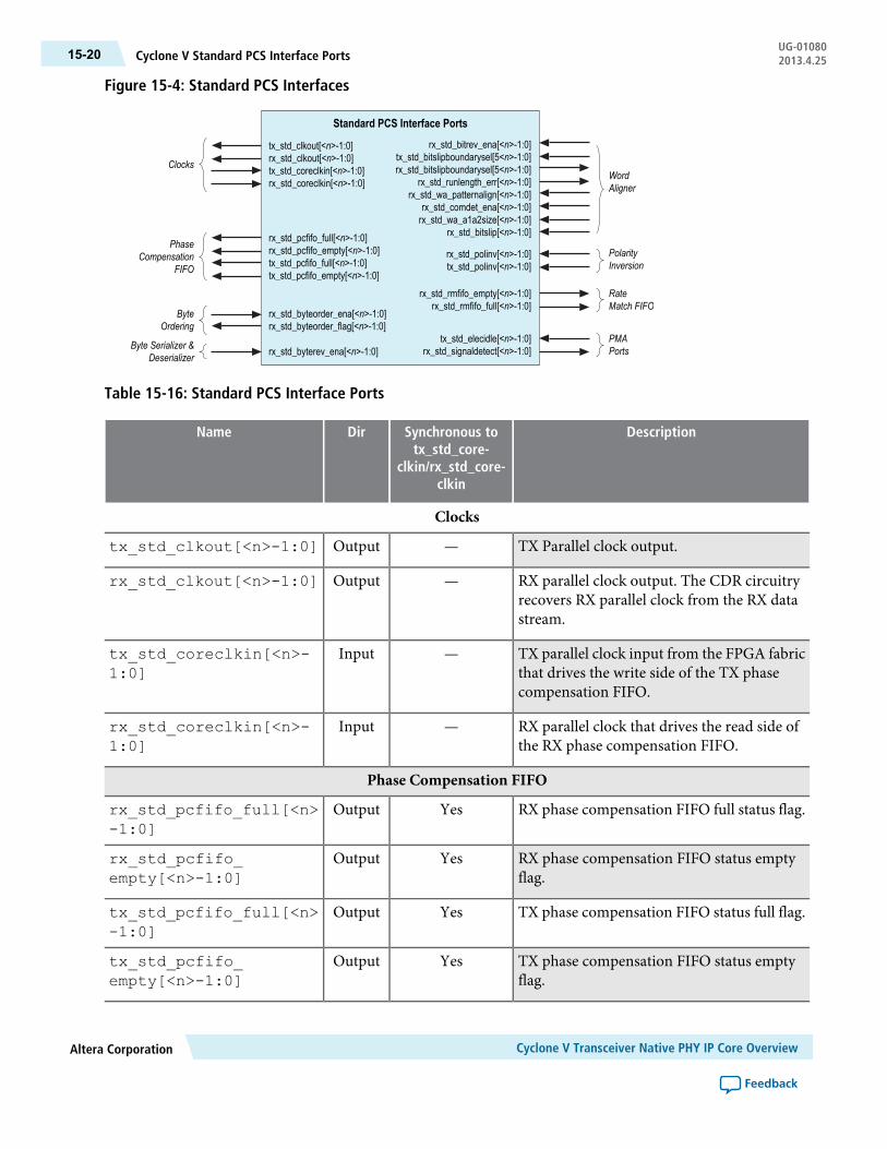
Figure 15-4: Standard PCS Interfaces
tx_std_clkout[<n>-1:0]rx_std_clkout[<n>-1:0]tx_std_coreclkin[<n>-1:0]rx_std_coreclkin[<n>-1:0]
ClocksWordAligner
rx_std_pcfifo_full[<n>-1:0]rx_std_pcfifo_empty[<n>-1:0]tx_std_pcfifo_full[<n>-1:0]tx_std_pcfifo_empty[<n>-1:0]
PhaseCompensation
FIFO
rx_std_byteorder_ena[<n>-1:0]rx_std_byteorder_flag[<n>-1:0]
ByteOrdering
rx_std_rmfifo_empty[<n>-1:0]rx_std_rmfifo_full[<n>-1:0]
RateMatch FIFO
rx_std_polinv[<n>-1:0]tx_std_polinv[<n>-1:0]
PolarityInversion
PMAPorts
Standard PCS Interface Portsrx_std_bitrev_ena[<n>-1:0]
tx_std_bitslipboundarysel[5<n>-1:0]rx_std_bitslipboundarysel[5<n>-1:0]
rx_std_runlength_err[<n>-1:0]rx_std_wa_patternalign[<n>-1:0]
rx_std_comdet_ena[<n>-1:0]rx_std_wa_a1a2size[<n>-1:0]
rx_std_bitslip[<n>-1:0]
tx_std_elecidle[<n>-1:0]rx_std_signaldetect[<n>-1:0]rx_std_byterev_ena[<n>-1:0]Byte Serializer &
Deserializer
Table 15-16: Standard PCS Interface Ports
DescriptionSynchronous totx_std_core-
clkin/rx_std_core-clkin
DirName
Clocks
TX Parallel clock output.—Outputtx_std_clkout[<n>-1:0]
RX parallel clock output. The CDR circuitryrecovers RX parallel clock from the RX datastream.
—Outputrx_std_clkout[<n>-1:0]
TX parallel clock input from the FPGA fabricthat drives the write side of the TX phasecompensation FIFO.
—Inputtx_std_coreclkin[<n>-1:0]
RX parallel clock that drives the read side ofthe RX phase compensation FIFO.
—Inputrx_std_coreclkin[<n>-1:0]
Phase Compensation FIFO
RX phase compensation FIFO full status flag.YesOutputrx_std_pcfifo_full[<n>-1:0]
RX phase compensation FIFO status emptyflag.
YesOutputrx_std_pcfifo_empty[<n>-1:0]
TX phase compensation FIFO status full flag.YesOutputtx_std_pcfifo_full[<n>-1:0]
TX phase compensation FIFO status emptyflag.
YesOutputtx_std_pcfifo_empty[<n>-1:0]
Cyclone V Transceiver Native PHY IP Core OverviewAltera Corporation
Feedback
UG-01080Cyclone V Standard PCS Interface Ports15-20 2013.4.25
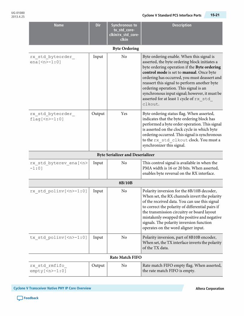
DescriptionSynchronous totx_std_core-
clkin/rx_std_core-clkin
DirName
Byte Ordering
Byte ordering enable. When this signal isasserted, the byte ordering block initiates abyte ordering operation if the Byte orderingcontrol mode is set to manual. Once byteordering has occurred, you must deassert andreassert this signal to perform another byteordering operation. This signal is ansynchronous input signal; however, it must beasserted for at least 1 cycle of rx_std_clkout.
NoInputrx_std_byteorder_ena[<n>-1:0]
Byte ordering status flag. When asserted,indicates that the byte ordering block hasperformed a byte order operation. This signalis asserted on the clock cycle in which byteordering occurred. This signal is synchronousto the rx_std_clkout clock. You must asynchronizer this signal.
YesOutputrx_std_byteorder_flag[<n>-1:0]
Byte Serializer and Deserializer
This control signal is available in when thePMA width is 16 or 20 bits. When asserted,enables byte reversal on the RX interface.
NoInputrx_std_byterev_ena[<n>-1:0]
8B/10B
Polarity inversion for the 8B/10B decoder,When set, the RX channels invert the polarityof the received data. You can use this signalto correct the polarity of differential pairs ifthe transmission circuitry or board layoutmistakenly swapped the positive and negativesignals. The polarity inversion functionoperates on the word aligner input.
NoInputrx_std_polinv[<n>-1:0]
Polarity inversion, part of 8B10B encoder,When set, the TX interface inverts the polarityof the TX data.
NoInputtx_std_polinv[<n>-1:0]
Rate Match FIFO
Rate match FIFO empty flag. When asserted,the rate match FIFO is empty.
NoOutputrx_std_rmfifo_empty[<n>-1:0]
Altera CorporationCyclone V Transceiver Native PHY IP Core Overview
Feedback
15-21Cyclone V Standard PCS Interface PortsUG-010802013.4.25
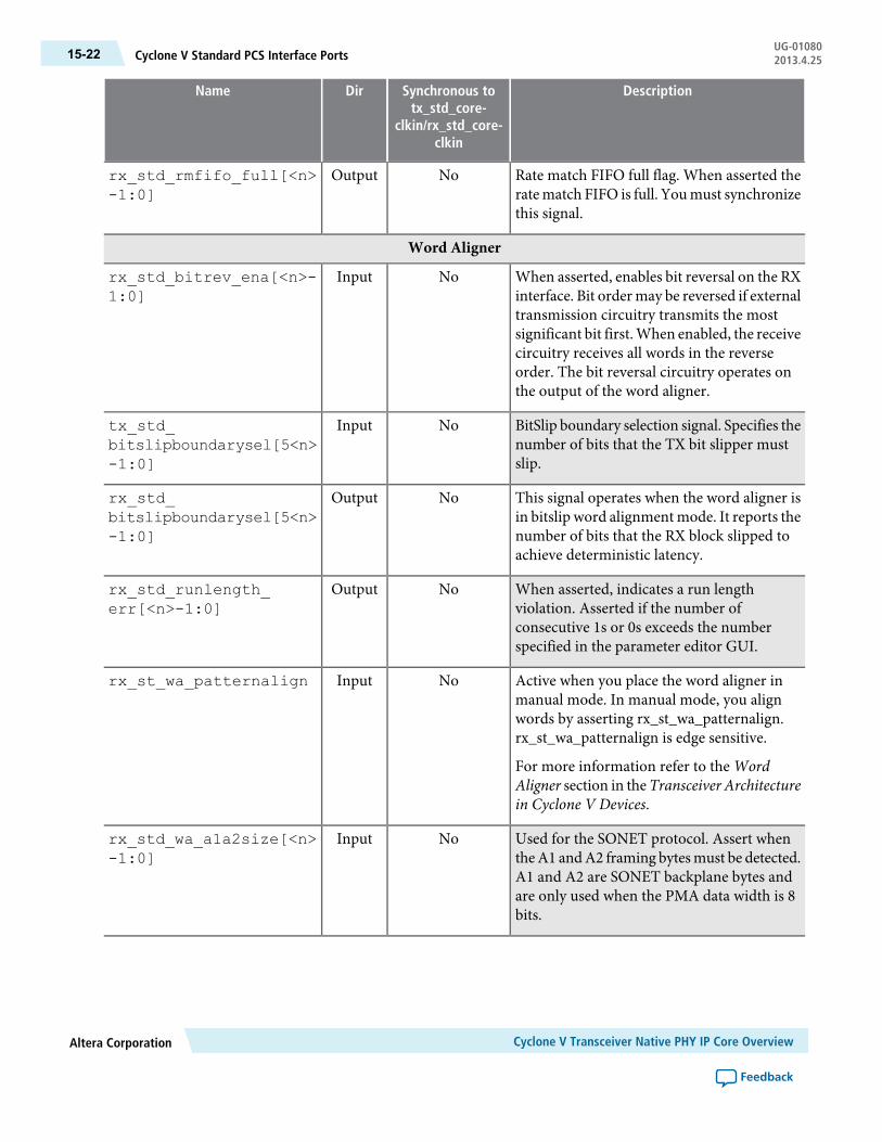
DescriptionSynchronous totx_std_core-
clkin/rx_std_core-clkin
DirName
Rate match FIFO full flag. When asserted theratematch FIFO is full. Youmust synchronizethis signal.
NoOutputrx_std_rmfifo_full[<n>-1:0]
Word Aligner
When asserted, enables bit reversal on the RXinterface. Bit order may be reversed if externaltransmission circuitry transmits the mostsignificant bit first.When enabled, the receivecircuitry receives all words in the reverseorder. The bit reversal circuitry operates onthe output of the word aligner.
NoInputrx_std_bitrev_ena[<n>-1:0]
BitSlip boundary selection signal. Specifies thenumber of bits that the TX bit slipper mustslip.
NoInputtx_std_bitslipboundarysel[5<n>-1:0]
This signal operates when the word aligner isin bitslip word alignment mode. It reports thenumber of bits that the RX block slipped toachieve deterministic latency.
NoOutputrx_std_bitslipboundarysel[5<n>-1:0]
When asserted, indicates a run lengthviolation. Asserted if the number ofconsecutive 1s or 0s exceeds the numberspecified in the parameter editor GUI.
NoOutputrx_std_runlength_err[<n>-1:0]
Active when you place the word aligner inmanual mode. In manual mode, you alignwords by asserting rx_st_wa_patternalign.rx_st_wa_patternalign is edge sensitive.
For more information refer to the WordAligner section in theTransceiver Architecturein Cyclone V Devices.
NoInputrx_st_wa_patternalign
Used for the SONET protocol. Assert whentheA1 andA2 framing bytesmust be detected.A1 and A2 are SONET backplane bytes andare only used when the PMA data width is 8bits.
NoInputrx_std_wa_a1a2size[<n>-1:0]
Cyclone V Transceiver Native PHY IP Core OverviewAltera Corporation
Feedback
UG-01080Cyclone V Standard PCS Interface Ports15-22 2013.4.25

DescriptionSynchronous totx_std_core-
clkin/rx_std_core-clkin
DirName
Usedwhenword alignermode is bitslipmode.For every rising edge of the rx_std_bitslip signal, theword boundary is shiftedby 1 bit. Each bitslip removes the earliestreceived bit from the received data. You mustsynchronize this signal.
NoInputrx_std_bitslip[<n>-1:0]
Miscellaneous
When asserted, enables a circuit to detect adownstream receiver. This signal must bedriven low when not in use because it causesthe TXPMA to enter electrical idlemodewiththe TX serial data signals in tristate mode.
Inputtx_std_elecidle[<n>-1:0]
Signal threshold detect indicator. Whenasserted, it indicates that the signal present atthe receiver input buffer is above theprogrammed signal detection threshold value.You must synchronize this signal.
NoOutputrx_std_signaldetect[<n>-1:0]
Related InformationTransceiver Architecture in Cyclone V Devices
SDC Timing ConstraintsThis section describes SDC timing constraints for the Cyclone V Native PHY.
TheQuartus II 12.1 software reports timing violations for asynchronous inputs to the Standard PCS. Becausemany violations are for asynchronous paths, they do not represent actual timing failures. You may chooseone of the following three approaches to identify these false timing paths to the Quartus II or TimeQuestsoftware.
• You can cut these paths in your SynopsysDesignConstraints (.sdc) file by using theset_false_pathcommand as shown in the following example.
Example 15-1: Using the set_false_path Constraint to Identify Asynchronous Inputs
set_false_path -through {*8gbitslip*} -to [get_registers*8g_rx_pcs*SYNC_DATA_REG*]set_false_path -through {*8gbytordpld*} -to [get_registers*8g_rx_pcs*SYNC_DATA_REG*]set_false_path -through {*8gcmpfifoburst*} -to [get_registers*8g_rx_pcs*SYNC_DATA_REG*]set_false_path -through {*8gphfifoburstrx*} -to [get_registers
Altera CorporationCyclone V Transceiver Native PHY IP Core Overview
Feedback
15-23SDC Timing ConstraintsUG-010802013.4.25

*8g_rx_pcs*SYNC_DATA_REG*]
set_false_path -through {*8gsyncsmen*} -to [get_registers*8g*pcs*SYNC_DATA_REG*]set_false_path -through {*8gwrdisablerx*} -to [get_registers*8g_rx_pcs*SYNC_DATA_REG*]set_false_path -through {*rxpolarity*} -to [get_registers*SYNC_DATA_REG*]set_false_path -through {*pldeidleinfersel*} -to [get_registers*SYNC_DATA_REG*]
• You can use the set_max_delay constraint on a given path to create a constraint for asynchronoussignals that do not have a specific clock relationship but require a maximum path delay.
Example 15-2: Using the max_delay Constraint to Identify Asynchronous Inputs
# Example: Apply 10ns max delayset_max_delay -from *tx_from_fifo* -to *8g*pcs*SYNC_DATA_REG1 10
• You can use the set_false path command only during Timequest timing analysis.
Example 15-3: Using the set_false TimeQuest Constraint to Identify Asynchronous Inputs
#if {$::TimeQuestInfo(nameofexecutable) eq "quartus_fit"} {#} else {#set_false_path -from [get_registers {*tx_from_fifo*}] -through{*txbursten*} -to [get_registers *8g_*_pcs*SYNC_DATA_REG
In in all of these examples, you must substitute your actual signal names for the signal names shown.Note:
Dynamic ReconfigurationDynamic reconfiguration calibrates each channel to compensate for variations due to process, voltage, andtemperature (PVT).
These process variations result in analog voltages that can be offset from required ranges. The calibrationperformed by the dynamic reconfiguration interface compensates for variations due to PVT.
For non-bonded clocks, each channel and each TX PLL has a separate dynamic reconfiguration interfaces.The MegaWizard Plug-In Manager provides informational messages on the connectivity of these interfaces.The following example shows the messages for the Cyclone V Native PHY with four duplex channels, fourTX PLLs, in a nonbonded configuration.
For more information about transceiver reconfiguration refer to Transceiver Reconfiguration Controller IPCore.
Cyclone V Transceiver Native PHY IP Core OverviewAltera Corporation
Feedback
UG-01080Dynamic Reconfiguration15-24 2013.4.25

Example 15-4: Informational Messages for the Transceiver Reconfiguration Interface
PHY IP will require 8 reconfiguration interfaces for connectionto the external reconfiguration controller.Reconfiguration interface offsets 0-3 are connected to thetransceiver channels.Reconfiguration interface offsets 4–7 are connected to thetransmit PLLs.
Related InformationTransceiver Architecture in Cyclone V Devices
Simulation SupportThe Quartus II 12.1 release provides simulation and compilation support for the Native PHY IP Core. Referto Running a Simulation Testbench for a description of the directories and files that the Quartus II softwarecreates automatically when you generate your Native PHY IP Core.
Related InformationRunning a Simulation Testbench on page 1-6
Altera CorporationCyclone V Transceiver Native PHY IP Core Overview
Feedback
15-25Simulation SupportUG-010802013.4.25

16Transceiver Reconfiguration Controller IPCore Overview
2013.4.25UG-01080 Subscribe Feedback
The Altera Transceiver Reconfiguration Controller dynamically reconfigures analog settings in Arria V,Arria V GZ, Cyclone V, and Stratix V devices. Dynamic reconfiguration allows you to compensate forvariations due to process, voltage, and temperature (PVT) in 28-nm devices.
Dynamic reconfiguration is required for Arria V, Arria V GZ, Cyclone V, and Stratix V devices that includetransceivers. The reconfiguration functionality available in Arria V and Cyclone V devices is a subset of thefunctionality available for Stratix V devices.
Some of the reconfiguration features not available for Arria V and Cyclone V devices in the currentrelease, may be available in subsequent releases. Arria V and Cyclone V devices do not include ATXPLLs. Stratix V and Arria V GZ devices include ATX PLLs.
Note:
Table 16-1: Device Support for Dynamic Reconfiguration
Cyclone VArria V GZArria VStratix VFeatureArea
YesYesYesYesOffset cancellationCalibrationFunctions Yes—Yes—Duty cycle distortion calibration
—Yes—YesATX PLL calibration
—Yes—YesOn-chip signal quality monitoring
Analog Features —Yes—YesDecision feedback equalization (DFE)
—Yes—YesAdaptive equalization
YesYesYesYesPre-CDR reverse serial loopbackLoopbackmodes YesYesYesYesPost-CDR reverse serial loopback
YesYesYesYesReference clock switching (CDR,ATXPLLs, and TX PLLs)PLL
reconfiguration YesYesYesYesTX PLL connected to a transceiverchannel reconfiguration
ISO9001:2008Registered
© 2013 Altera Corporation. All rights reserved. ALTERA, ARRIA, CYCLONE, HARDCOPY, MAX, MEGACORE, NIOS, QUARTUS and STRATIXwords and logos are trademarks of Altera Corporation and registered in the U.S. Patent and Trademark Office and in other countries. All other wordsand logos identified as trademarks or service marks are the property of their respective holders as described at www.altera.com/common/legal.html.Altera warrants performance of its semiconductor products to current specifications in accordance with Altera's standard warranty, but reserves theright to make changes to any products and services at any time without notice. Altera assumes no responsibility or liability arising out of the applicationor use of any information, product, or service described herein except as expressly agreed to in writing by Altera. Altera customers are advised toobtain the latest version of device specifications before relying on any published information and before placing orders for products or services.
www.altera.com
101 Innovation Drive, San Jose, CA 95134

Cyclone VArria V GZArria VStratix VFeatureArea
YesYesYesYesRX CDR reconfiguration
TransceiverChannel/PLLReconfiguration
YesYesYesYesReconfiguration of PCS blocks
—Yes—YesTX PLL switching
—Yes—YesATX PLL switching
YesYesYesYesTX local clock divider reconfiguration(1,2,4,8)
YesYesYesYesFPGA fabric-transceiver channel datawidth reconfiguration
For more information about the features that are available for each device refer to the following devicedocumentation:Dynamic Reconfiguration in Stratix VDevices,Dynamic Reconfiguration in Arria VDevices,and Dynamic Reconfiguration in Cyclone V Devices. These chapters are included in the Stratix V, Arria V,and Cyclone V device handbooks, respectively.
Related InformationDynamic Reconfiguration in Stratix V Devices
Dynamic Reconfiguration in Arria V Devices
Dynamic Reconfiguration in Cyclone V Devices
Transceiver Reconfiguration Controller System OverviewThis section describes the Transceiver Reconfiguration Controller’s role. You can include the embeddedcontroller that initiates reconfiguration in your FPGA or use an embedded processor on the PCB.
Transceiver Reconfiguration Controller IP Core OverviewAltera Corporation
Feedback
UG-01080Transceiver Reconfiguration Controller System Overview16-2 2013.4.25

Figure 16-1: Transceiver Reconfiguration Controller
to and fromEmbeddedController
TX and RXSerial Data
Avalon-MM master interface
TransceiverReconfiguration
ControllerS
M Avalon-MM slave interfaceS
reconfig_to_xcvr[<n>:0]
reconfig_mif_address[31:0]reconfig_mif_read
ReconfigurationManagementInterface
reconfig_mif_readdata[15:0]reconfig_mif_waitrequest
Streaming Data
reconfig_from_xcvr[<n>:0]
Transceiver PHY
Registers toreconfigure
User ApplicationIncluding MAC
Altera V-Series FPGA
.
.
.
.
.
.
SMMaster
M
S
MIFROM
An embedded controller programs the Transceiver Reconfiguration Controller using its Avalon-MM slaveinterface. Thereconfig_to_xcvr andreconfig_from_xcvrbuses include theAvalon-MMaddress,read, write, readdata, writedata, and signals that connect to features related to calibration and signal integrity.
The Transceiver Reconfiguration Controller provides two modes to dynamically reconfigure transceiversettings:
• Register Based—In this access mode you can directly reconfigure a transceiver PHY IP core using theTransceiver Reconfiguration Controller’s reconfiguration management interface. You initiatereconfiguration using a series of Avalon-MM reads and writes to the appropriate registers of theTransceiver ReconfigurationController. The Transceiver ReconfigurationController translates the deviceindependent commands received on the reconfiguration management interface to device dependentcommands on the transceiver reconfiguration interface. For more information, refer to ChangingTransceiver Settings Using Register-Based Reconfiguration.
For more information about Avalon-MM interfaces including timing diagrams, refer to the AvalonInterface Specifications.
• Streamer Based —This access mode allows you to either stream a MIF that contains the reconfigurationdata or performdirect writes to perform reconfiguration. The streamingmode uses amemory initializationfile (.mif) to stream an update to the transceiver PHY IP core. The .mif file can contain changes for manysettings. For example, a single .mif filemight contain changes to the PCS datapath settings, clock settings,and PLL parameters. You specify the .mif using write commands on the Avalon-MM PHY managementinterface. After the streaming operation is specified, the update proceeds in a single step. For moreinformation, refer to Changing Transceiver Settings Using Streamer-Based Reconfiguration. In the directwrite mode, you perform Avalon-MM reads and writes to initiate a reconfiguration of the PHY IP. Formore information, refer to Direct Write Reconfiguration.
Altera CorporationTransceiver Reconfiguration Controller IP Core Overview
Feedback
16-3Transceiver Reconfiguration Controller System OverviewUG-010802013.4.25
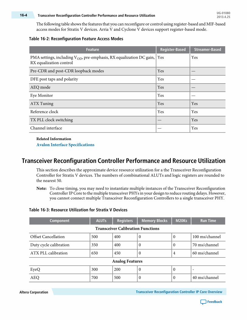
The following table shows the features that you can reconfigure or control using register-based andMIF-basedaccess modes for Stratix V devices. Arria V and Cyclone V devices support register-based mode.
Table 16-2: Reconfiguration Feature Access Modes
Streamer-BasedRegister-BasedFeature
YesYesPMA settings, including VOD, pre-emphasis, RX equalization DC gain,RX equalization control
—YesPre-CDR and post-CDR loopback modes
—YesDFE post taps and polarity
—YesAEQ mode
—YesEye Monitor
YesYesATX Tuning
YesYesReference clock
Yes—TX PLL clock switching
Yes—Channel interface
Related InformationAvalon Interface Specifications
Transceiver Reconfiguration Controller Performance and Resource UtilizationThis section describes the approximate device resource utilization for a the Transceiver ReconfigurationController for Stratix V devices. The numbers of combinational ALUTs and logic registers are rounded tothe nearest 50.
To close timing, you may need to instantiate multiple instances of the Transceiver ReconfigurationController IPCore to themultiple transceiver PHYs in your design to reduce routing delays. However,you cannot connect multiple Transceiver Reconfiguration Controllers to a single transceiver PHY.
Note:
Table 16-3: Resource Utilization for Stratix V Devices
Run TimeM20KsMemory BlocksRegistersALUTsComponent
Transceiver Calibration Functions
100 ms/channel00400500Offset Cancellation
70 ms/channel00400350Duty cycle calibration
60 ms/channel40450650ATX PLL calibration
Analog Features
-00200300EyeQ
40 ms/channel00500700AEQ
Transceiver Reconfiguration Controller IP Core OverviewAltera Corporation
Feedback
UG-01080Transceiver Reconfiguration Controller Performance and Resource Utilization16-4 2013.4.25

Run TimeM20KsMemory BlocksRegistersALUTsComponent
Reconfiguration Features
- 500500400Channel andPLL reconfiguration
00350250PLL reconfiguration (only)
Parameterizing the Transceiver Reconfiguration Controller IP Core in theMegaWizard Plug-In Manager
Complete the following steps to configure the Transceiver Reconfiguration Controller IP Core in theMegaWizard Plug-In Manager:
1. For Which device family will you be using?, select Arria V, Arria V GZ, Cyclone V, or Stratix V fromthe list.
2. Click Installed Plug-Ins > Interfaces > Transceiver PHY >Transceiver Reconfiguration Controllerv12.1.
3. Select the options required for your design. For a description of these options, refer to theGeneralOptionsParameters.
4. Click Finish to generate your customized Transceiver Reconfiguration Controller PHY IP Core.
Parameterizing the Transceiver Reconfiguration Controller IP Core in QsysComplete the following steps to configure the Transceiver Reconfiguration Controller IP Core in Qsys:
1. On the Project Settings tab, select Arria V, Arria V GZ, Cyclone V, or Stratix V from the list.2. On the Component Library tab, type the following text string in the search box: reconfig. Qsys filters
the component library and shows all components matching the text string you entered.3. Click Transceiver Reconfiguration Controller and then click +Add.4. Select the options required for your design. For a description of these options, refer to theGeneralOptions
Parameters.5. Click Finish to generate your customized Transceiver Reconfiguration Controller PHY IP Core.
General Options ParametersThis section lists the available options.
Table 16-4: General Options
DescriptionValueName
Specifies the device family. The reconfiguration functionsavailable for Arria V and Cyclone V devices are a subsetof those available for Stratix V devices. Refer to DeviceSupport for Dynamic Reconfiguration for moreinformation about available functions.
Arria V
Arria V GZ
Cyclone V
Stratix V
Device family
5 The time to complete these functions depends upon the complexity of the reconfiguration operation.
Altera CorporationTransceiver Reconfiguration Controller IP Core Overview
Feedback
16-5Parameterizing the Transceiver Reconfiguration Controller IP Core in the MegaWizard Plug-In ManagerUG-010802013.4.25
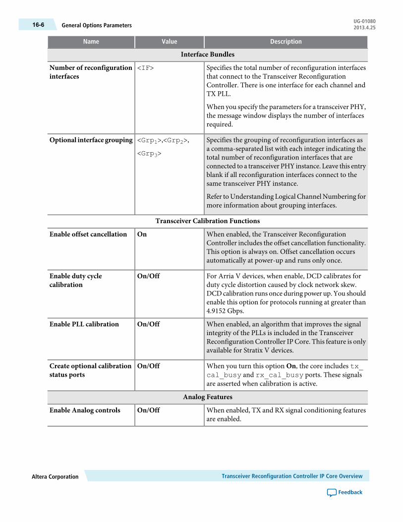
DescriptionValueName
Interface Bundles
Specifies the total number of reconfiguration interfacesthat connect to the Transceiver ReconfigurationController. There is one interface for each channel andTX PLL.
When you specify the parameters for a transceiver PHY,the message window displays the number of interfacesrequired.
<IF>Number of reconfigurationinterfaces
Specifies the grouping of reconfiguration interfaces asa comma-separated list with each integer indicating thetotal number of reconfiguration interfaces that areconnected to a transceiver PHY instance. Leave this entryblank if all reconfiguration interfaces connect to thesame transceiver PHY instance.
Refer toUnderstanding Logical ChannelNumbering formore information about grouping interfaces.
<Grp1>,<Grp2>,
<Grp3>
Optional interface grouping
Transceiver Calibration Functions
When enabled, the Transceiver ReconfigurationController includes the offset cancellation functionality.This option is always on. Offset cancellation occursautomatically at power-up and runs only once.
OnEnable offset cancellation
For Arria V devices, when enable, DCD calibrates forduty cycle distortion caused by clock network skew.DCDcalibration runs once during power up. You shouldenable this option for protocols running at greater than4.9152 Gbps.
On/OffEnable duty cyclecalibration
When enabled, an algorithm that improves the signalintegrity of the PLLs is included in the TransceiverReconfigurationController IPCore. This feature is onlyavailable for Stratix V devices.
On/OffEnable PLL calibration
When you turn this option On, the core includes tx_cal_busy and rx_cal_busy ports. These signalsare asserted when calibration is active.
On/OffCreate optional calibrationstatus ports
Analog Features
When enabled, TX and RX signal conditioning featuresare enabled.
On/OffEnable Analog controls
Transceiver Reconfiguration Controller IP Core OverviewAltera Corporation
Feedback
UG-01080General Options Parameters16-6 2013.4.25

DescriptionValueName
When enabled, you can use the EyeQ, the on-chip signalquality monitoring circuitry, to estimate the actual eyeopening at the receiver. This feature is only available forStratix V devices.
On/OffEnable EyeQ block
When you turn this option On, the TransceiverReconfiguration Controller includes logic to performDFE
On/OffEnable decision feedbackequalizer (DFE) block
When enabled, the Transceiver ReconfigurationController includes logic to perform AEQ. This featureis only available for Stratix V devices.
On/OffEnable adaptiveequalization (AEQ) block
Reconfiguration Features
When enabled, the Transceiver ReconfigurationController includes logic to include both channel andPLL reconfiguration.
On/OffEnable channel/PLLreconfiguration
When enabled, the Transceiver ReconfigurationController includes logic to perform PLLreconfiguration.
On/OffEnable PLL reconfigurationsupport block
Transceiver Reconfiguration Controller InterfacesThis section describes the top-level signals of the Transceiver Reconfiguration Controller.
Figure 16-2: Top-Level Signals of the Transceiver Reconfiguration Controller
Transceiver Reconfiguration Controller Top-Level Signals
ReconfigurationManagement
Avalon-MM SlaveInterface
MIF ReconfigurationAvalon-MM Master
InterfaceTransceiver
Reconfiguration
reconfig_mif_address[31:0]reconfig_mif_readreconfig_mif_readdata[15:0]reconfig_mif_waitrequestcal_busy_in
mgmt_clk_clkmgmt_rst_resetreconfig_mgmt_address[6:0]reconfig_mgmt_writedata[31:0]reconfig_mgmt_readdata[31:0]reconfig_mgmt_writereconfig_mgmt_readreconfig_mgmt_waitrequest
reconfig_to_xcvr[(<n> 70-1):0]reconfig_from_xcvr[(<n> 46-1):0]
reconfig_busytx_cal_busyrx_cal_busy
By default, the Block Diagram shown in the MegaWizard Plug-In Manager labels the external pinswith the interface type and places the interface name inside the box. The interface type and name are
Note:
used in the Hardware Component Description File (_hw.tcl). If you click Show signals, the blockdiagram expands to show all of the signals of the component given the options currently selected inthe MegaWizard Plug-In Manager.
For more information about _hw.tcl files refer to the Component Interface Tcl Reference in volume 1 of theQuartus II Handbook.
Altera CorporationTransceiver Reconfiguration Controller IP Core Overview
Feedback
16-7Transceiver Reconfiguration Controller InterfacesUG-010802013.4.25
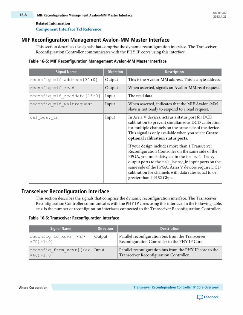
Related InformationComponent Interface Tcl Reference
MIF Reconfiguration Management Avalon-MM Master InterfaceThis section describes the signals that comprise the dynamic reconfiguration interface. The TransceiverReconfiguration Controller communicates with the PHY IP cores using this interface.
Table 16-5: MIF Reconfiguration Management Avalon-MM Master Interface
DescriptionDirectionSignal Name
This is theAvalon-MMaddress. This is a byte address.Outputreconfig_mif_address[31:0]
When asserted, signals an Avalon-MM read request.Outputreconfig_mif_read
The read data.Inputreconfig_mif_readdata[15:0]
When asserted, indicates that the MIF Avalon-MMslave is not ready to respond to a read request.
Inputreconfig_mif_waitrequest
In Arria V devices, acts as a status port for DCDcalibration to prevent simultaneous DCD calibrationfor multiple channels on the same side of the device.This signal is only available when you select Createoptional calibration status ports.
If your design includes more than 1 TransceiverReconfiguration Controller on the same side of theFPGA, you must daisy chain the tx_cal_busyoutput ports to the cal_busy_in input ports on thesame side of the FPGA. Arria V devices require DCDcalibration for channels with data rates equal to orgreater than 4.9152 Gbps.
Inputcal_busy_in
Transceiver Reconfiguration InterfaceThis section describes the signals that comprise the dynamic reconfiguration interface. The TransceiverReconfiguration Controller communicates with the PHY IP cores using this interface. In the following table,<n> is the number of reconfiguration interfaces connected to the Transceiver Reconfiguration Controller.
Table 16-6: Transceiver Reconfiguration Interface
DescriptionDirectionSignal Name
Parallel reconfiguration bus from the TransceiverReconfiguration Controller to the PHY IP Core.
Outputreconfig_to_xcvr[(<n>×70)-1:0]
Parallel reconfiguration bus from the PHY IP core to theTransceiver Reconfiguration Controller.
Inputreconfig_from_xcvr[(<n>×46)-1:0]
Transceiver Reconfiguration Controller IP Core OverviewAltera Corporation
Feedback
UG-01080MIF Reconfiguration Management Avalon-MM Master Interface16-8 2013.4.25
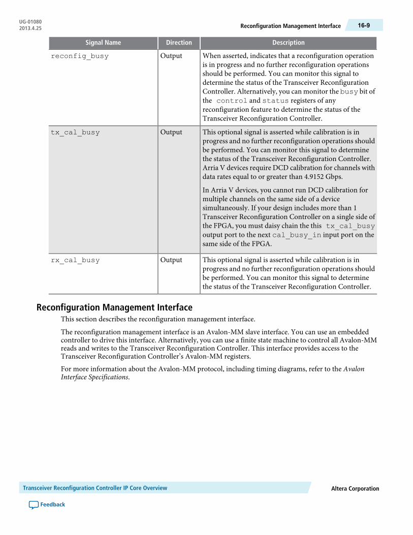
DescriptionDirectionSignal Name
When asserted, indicates that a reconfiguration operationis in progress and no further reconfiguration operationsshould be performed. You can monitor this signal todetermine the status of the Transceiver ReconfigurationController. Alternatively, you can monitor the busy bit ofthe control and status registers of anyreconfiguration feature to determine the status of theTransceiver Reconfiguration Controller.
Outputreconfig_busy
This optional signal is asserted while calibration is inprogress and no further reconfiguration operations shouldbe performed. You can monitor this signal to determinethe status of the Transceiver Reconfiguration Controller.Arria V devices require DCD calibration for channels withdata rates equal to or greater than 4.9152 Gbps.
In Arria V devices, you cannot run DCD calibration formultiple channels on the same side of a devicesimultaneously. If your design includes more than 1Transceiver Reconfiguration Controller on a single side ofthe FPGA, you must daisy chain the this tx_cal_busyoutput port to the next cal_busy_in input port on thesame side of the FPGA.
Outputtx_cal_busy
This optional signal is asserted while calibration is inprogress and no further reconfiguration operations shouldbe performed. You can monitor this signal to determinethe status of the Transceiver Reconfiguration Controller.
Outputrx_cal_busy
Reconfiguration Management InterfaceThis section describes the reconfiguration management interface.
The reconfiguration management interface is an Avalon-MM slave interface. You can use an embeddedcontroller to drive this interface. Alternatively, you can use a finite state machine to control all Avalon-MMreads and writes to the Transceiver Reconfiguration Controller. This interface provides access to theTransceiver Reconfiguration Controller’s Avalon-MM registers.
For more information about the Avalon-MM protocol, including timing diagrams, refer to the AvalonInterface Specifications.
Altera CorporationTransceiver Reconfiguration Controller IP Core Overview
Feedback
16-9Reconfiguration Management InterfaceUG-010802013.4.25
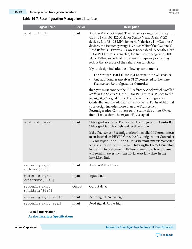
Table 16-7: Reconfiguration Management Interface
DescriptionDirectionSignal Name
Avalon-MM clock input. The frequency range for the mgmt_clk_clk is 100-125 MHz for Stratix V and Arria V GZdevices. It is 75-125 MHz for Arria V devices. For Cyclone Vdevices, the frequency range is 75-125MHz if the Cyclone VHard IP for PCI Express IPCore is not enabled.When theHardIP for PCI Express is enabled, the frequency range is 75-100MHz. Falling outside of the required frequency range mayreduce the accuracy of the calibration functions.
If your design includes the following components:
• The Stratix V Hard IP for PCI Express with CvP enabled• Any additional transceiver PHY connected to the same
Transceiver Reconfiguration Controller
then you must connect the PLL reference clock which is calledrefclk in the Stratix V Hard IP for PCI Express IP Core to themgmt_clk_clk signal of the Transceiver ReconfigurationController and the additional transceiver PHY. In addition, ifyour design includes more than one TransceiverReconfiguration Controllers on the same side of the FPGA,they all must share the mgmt_clk_clk signal
Inputmgmt_clk_clk
This signal resets the Transceiver Reconfiguration Controller.This signal is active high and level sensitive.
If the Transceiver ReconfigurationController IPCore connectsto an Interlaken PHY IP Core, the Reconfiguration ControllerIPCoremgmt_rst_reset must be simultaneously assertedwithphy_mgmt_clk_reset to bring theFrameGeneratorsin the link into alignment. Failure to meet to this requirementwill result in excessive transmit lane-to-lane skew in theInterlaken link.
Inputmgmt_rst_reset
Avalon-MM address.Inputreconfig_mgmt_address[6:0]
Input data.Inputreconfig_mgmt_writedata[31:0]
Output data.Outputreconfig_mgmt_readdata[31:0]
Write signal. Active high.Inputreconfig_mgmt_write
Read signal. Active high.Inputreconfig_mgmt_read
Related InformationAvalon Interface Specifications
Transceiver Reconfiguration Controller IP Core OverviewAltera Corporation
Feedback
UG-01080Reconfiguration Management Interface16-10 2013.4.25
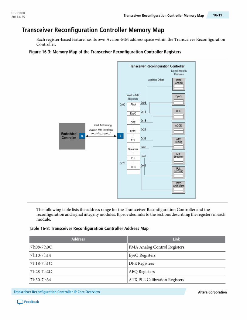
Transceiver Reconfiguration Controller Memory MapEach register-based feature has its own Avalon-MM address space within the Transceiver ReconfigurationController.
Figure 16-3: Memory Map of the Transceiver Reconfiguration Controller Registers
Direct Addressing
Address Offset
0x00
0x13
0x0B
0x1B
0x2B
0x33
0x3B
0x43
0x480x7F
Transceiver Reconfiguration Controller
Avalon-MM Interfacereconfig_mgmt_*
Avalon-MMRegisters
Signal IntegrityFeatures
DFE
ADCE
ATXTuning
MIFStreamer
PLLReconfig
EyeQ
PMAAnalog
DCDCalibration
EyeQ
...
DFE
...
PMA
ADCE...
ATX
...
Streamer
...
PLL
DCD
...
SMEmbeddedController
...
The following table lists the address range for the Transceiver Reconfiguration Controller and thereconfiguration and signal integrity modules. It provides links to the sections describing the registers in eachmodule.
Table 16-8: Transceiver Reconfiguration Controller Address Map
LinkAddress
PMA Analog Control Registers7'h08-7'h0C
EyeQ Registers7'h10-7'h14
DFE Registers7'h18-7'h1C
AEQ Registers7'h28-7'h2C
ATX PLL Calibration Registers7'h30-7'h34
Altera CorporationTransceiver Reconfiguration Controller IP Core Overview
Feedback
16-11Transceiver Reconfiguration Controller Memory MapUG-010802013.4.25

LinkAddress
Streamer Module Registers7'h38-7'h3C
PLL Reconfiguration7'h40-7'h44
Transceiver Reconfiguration Controller Calibration FunctionsTheTransceiverReconfigurationController supports various calibration functions to enhance the performanceand operation of any connected transceiver PHY IP core. Refer to Resource Utilization for Stratix V Devicesfor the resource utilization of these calibration functions.
Offset CancellationThe offset cancellation function adjusts the offsets within the RX PMA and the CDR parameters for processvariations to achieve optimal performance.
Offset cancellation runs only once upon power-up. The RX buffers are unavailable while this function isrunning. This calibration feature is run automatically and enabled by default. Arria V and Cyclone V devicesdo not require offset cancellation for the RX buffer.
Duty Cycle CalibrationTheTX clocks generated by theCMUand travel across the clock networkmay introduce duty cycle distortion(DCD). DCD calibration function reduces this distortion.
DCD runs once during device power up and you can manually trigger DCD after power up. Alterarecommends that you enable DCD for Arria V and Cyclone V devices if either of the following conditionsis true:
• The data rate is greater than or equal to 4.9152 Gbps• The design dynamically reconfigures the TX PLL and the data rate is greater than or equal to 4.9152 Gbps
Related InformationAN 676: Using the Arria V and Cyclone V Reconfiguration Controller to Perform DynamicReconfiguration
Auxiliary Transmit (ATX) PLL CalibrationATX calibration tunes the parameters of the ATX PLL for optimal performance. This function runs onceafter power up. You can rerun this function by writing into the appropriate memory-mapped registers.
The RX buffer is unavailable while this function is running. You should run the ATX calibration afterreconfiguring the PLL. You may need to rerun ATX calibration if you reset an ATX PLL and it does not lockafter the specified lock time.
For more information about the Auxiliary Transmit (ATX) PLL Calibration refer to ATX PLL CalibrationRegisters.
Refer to the Parameterizing the Transceiver Reconfiguration Controller IP Core in the MegaWizard Plug-InManager section for information about how to enabled these functions.
Transceiver Reconfiguration Controller IP Core OverviewAltera Corporation
Feedback
UG-01080Transceiver Reconfiguration Controller Calibration Functions16-12 2013.4.25

Transceiver Reconfiguration Controller PMA Analog Control RegistersYou can use the Transceiver Reconfiguration Controller to reconfigure the following analog controls:
• Differential output voltage (VOD)• Pre-emphasis taps• Receiver equalization control• Receiver equalization DC gain• Reverse serial loopback
All undefined register bits are reserved.Note:
Table 16-9: PMA Analog Registers
DescriptionRegister NameR/WBitsReconfig Addr
The logical channel number.Must be specifiedwhen performing dynamic updates. TheTransceiver ReconfigurationControllermapsthe logical address to the physical address.
logical channelnumber
RW[9:0]7’h08
The physical channel address. TheTransceiverReconfiguration Controller maps the logicaladdress to the physical address.
physical channeladdress
R[9:0]7’h09
Error. When asserted, indicates an error.This bit is asserted if any of the followingconditions occur:
• The channel address is invalid.• The PHY address is invalid.• The PMA offset is invalid.
control and status
R[9]
7’h0ABusy. When asserted, indicates that areconfiguration operation is in progress.
R[8]
Read. Writing a 1 to this bit triggers a readoperation.
W[1]
Write. Writing a 1 to this bit triggers a writeoperation.
W[0]
Specifies the offset of the PMA analog settingto be reconfigured. Table 16-10 describes thevalid offset values.
pma offsetRW[5:0]7’h0B
Reconfiguration data for the PMA analogsettings. Refer to Table 16-10 for valid datavalues.
dataRW[6:0]7’h0C
Altera CorporationTransceiver Reconfiguration Controller IP Core Overview
Feedback
16-13Transceiver Reconfiguration Controller PMA Analog Control RegistersUG-010802013.4.25

Refer to the Arria V Device Datasheet, the Cyclone V Device Datasheet, or the Stratix V Device Datasheet formore information about the electrical characteristics of each device. The final values are currently pendingfull characterization of the silicon.
All undefined register bits are reserved and must be set to 0.Note:
Table 16-10: PMA Offsets and Values
DescriptionRegister NameR/WBitsOffset
VOD. The following encodings aredefined:
• 6’b000000:6’b111111:0–63
VODRW[5:0]0x0
The following encodings are defined:
• 5’b00000 and 5’b10000: 0• 5’b00001–5’b01111: -15 to -1• 5’b10001–5b’11111: 1 to 15
Pre-emphasis pre-tapRW[4:0]0x1
The following encodings are defined:
• 5’b00000–5’b11111: 0–31
Pre-emphasis first post-tapRW[4:0]0x2
The following encodings are defined:
• 5’b00000 and 5’b10000: 0• 5’b00001–5’b01111: -15 to -1• 5’b10001–5b’11111: 1 to 15
Pre-emphasis second post-tapRW[4:0]0x3
The following encodings are defined:
• 3’b000–3b’111:0–3• 3'b100-3'b111:4
RX equalization DC gainRW[2:0]0x10
The following encodings are defined:
• 4’b0000–4’b1111: 0–15
RX equalization controlRW[3:0]0x11
Writing a 1 to this bit enables reverse serialloopback. Writing a 0 disables pre-CDRreverse serial loopback.
Pre-CDR Reverse Serial LoopbackWO[0]0x20
Writing a 1 to this bit enables post-CDRreverse serial loopback. Writing a 0disables post-CDR reverse serial loopback.
Post-CDR Reverse Serial LoopbackWO[0]0x21
Refer to Changing Transceiver Settings Using Register-Based Reconfiguration and Changing TransceiverSettings Using Streamer-Based Reconfiguration for the procedures you can use to update PMA settings.
Related InformationArria V Device Datasheet
Cyclone V Device Datasheet
Transceiver Reconfiguration Controller IP Core OverviewAltera Corporation
Feedback
UG-01080Transceiver Reconfiguration Controller PMA Analog Control Registers16-14 2013.4.25

Stratix V Device Datasheet
Application Note 645: Dynamic Reconfiguration of PMA Controls in Stratix V Devices
Transceiver Reconfiguration Controller EyeQ RegistersEyeQ is a debug and diagnostic tool that analyzes the incoming data, including the receiver’s gain, noiselevel, and jitter after the receive buffer. EyeQ is only available for Stratix V and Arria V GZ devices.
EyeQ uses a phase interpolator and sampler to estimate the vertical and horizontal eye opening using thevalues that you specify for the horizontal phase and vertical height. (Refer to EyeQ Offsets and Values.) Thephase interpolator generates a sampling clock and the sampler examines the data from the receiver output.The sampled data is deserialized and sent to the IP core where the PRBS checker determines the BER. Asthe phase interpolator output clock phase is shifted by small increments, the data error rate goes from highto low to high if the receiver is good. The number of steps of valid data is defined as the width of the eye. Ifnone of the steps yields valid data, the width of the eye is equal to 0, which means the eye is closed.
If you are using the EyeQ monitor with DFE enabled, you must put the EyeQ monitor in 1D modeby writing the EyeQ 1D-eye bit. For more information, refer toTable 16-12 .
Note:
The following table lists the memory-mapped EyeQ registers that you can access using Avalon-MM readsand writes on reconfiguration management interface.
All undefined register bits are reserved.Note:
Table 16-11: Eye Monitor Registers
DescriptionRegister NameR/WBitsReconfig Addr
The logical channel number.Must be specifiedwhen performing dynamic updates. TheTransceiver ReconfigurationControllermapsthe logical address to the physical address.
logical channelnumber
RW[9:0]7’h10
The physical channel address. TheTransceiverReconfiguration Controller maps the logicaladdress to the physical address.
physical channeladdress
RW[9:0]7’h11
Error.When asserted, indicates an invalidchannel or address.
control and status
R[9]
7’h12
Busy. When asserted, indicates that areconfiguration operation is in progress.
R[8]
Read. Writing a 1 to this bit triggers a readoperation.
W[1]
Write. Writing a 1 to this bit triggers a writeoperation.
W[0]
Specifies the 6-bit offset of the EyeQ register.eyeq offsetRW[5:0]7’h13
Reconfiguration data for the transceiver PHYregisters.
dataRW[15:0]7’h14
Altera CorporationTransceiver Reconfiguration Controller IP Core Overview
Feedback
16-15Transceiver Reconfiguration Controller EyeQ RegistersUG-010802013.4.25

All undefined register bits are reserved and must be set to 0.Note:
Table 16-12: EyeQ Offsets and Values
DescriptionRegister NameR/WBitsOffset
Writing a 1 to this bit enables the Eye monitor.ControlRW[0]0x0
Taken together, the horizontal phase andvertical height specify the Cartesian x-ycoordinates of the point on the eye diagram that youwant to sample. You can increment through 64 phasesover 2 UI on the horizontal axis.
Horizontal phaseRW[5:0]0x1
Taken together, the horizontal phase andvertical height specify the Cartesian x-ycoordinates of the point on the eye diagram that youwant to sample. You can specify 64 heights on thevertical axis.
Vertical heightRW[5:0]0x2
You should not modify these bits. To update thisregister, first read the value of this register then changeonly the value for bits that are not reserved.
ReservedRMW[15:4]
0x3
Writing a 1 to this bit selects 1D Eye mode and disablesvertical height measurement. Writing a 0 to this bitselects normal 2D Eye measurement mode includingboth the horizontal and vertical axes. You must use 1DEye mode if you have enabled DFE.
1D-EyeRW[13]
You should not modify these bits. To update thisregister, first read the value of this register then changeonly the value for bits that are not reserved.
ReservedRMW[12:11]
Sets the EyeQbandwidth based on receiver channel datarate. The following encodings are defined:
• 2’b00: data rate < 1 Gbps• 2’b01: data rate > 1 Gbps and <= 2.5 Gbps• 2’b10: data rate > 2.5 Gbps and <= 7.5 Gbps• 2’b11: data rate > 7.5 Gbps
BandwidthRW[10:9]
You should notmodify these bits.To update this register,first read the value of this register then change only thevalue for bits that are not reserved.
ReservedRMW[8:0]
Refer to Changing Transceiver Settings Using Register-Based Reconfiguration for the procedures you canuse to control the Eye Monitor.
Transceiver Reconfiguration Controller IP Core OverviewAltera Corporation
Feedback
UG-01080Transceiver Reconfiguration Controller EyeQ Registers16-16 2013.4.25

Transceiver Reconfiguration Controller DFE RegistersThe DFE is an infinite impulse response filter (non-linear) that compensates for inter-symbol interference(ISI). Because the values of symbols previously detected are known, the DFE engine can estimate the ISIcontributed by these symbols and cancel out this ISI by subtracting the predicted value from subsequentsymbols.
This mechanism allows DFE to boost the signal to noise ratio of the received data. You can use DFE inconjunction with the receiver's linear equalization and with the transmitter's pre-emphasis feature. DFE isonly available for Stratix V devices.
DFE automatically runs offset calibration and phase interpolator (PI) phase calibration on all channels afterpower up. You can run DFE manually to determine the optimal settings by monitoring the BER of thereceived data at each setting and specify the DFE settings that yield the widest eye.
If you are using the EyeQ monitor with DFE enabled, you must put the EyeQ monitor in 1D modeby writing the EyeQ 1D-eye bit. For more information, refer to EyeQ Offsets and Values.
Note:
The following table lists the direct DFE registers that you can access using Avalon-MM reads and writes onreconfiguration management interface.
All undefined register bits are reserved.Note:
Table 16-13: DFE Registers
DescriptionRegister NameR/WBitsReconfig Addr
The logical channel address.Must be specifiedwhen performing dynamic updates. TheTransceiver ReconfigurationControllermapsthe logical address to the physical address.
logical channeladdress
RW[9:0]7’h18
The physical channel address. TheTransceiverReconfiguration Controller maps the logicaladdress to the physical address.
physical channeladdress
RW[9:0]7’h19
Error.When asserted, indicates an invalidchannel or address.
control and status
R[9]
7’h1A
Busy. When asserted, indicates that areconfiguration operation is in progress.
R[8]
Read. Writing a 1 to this bit triggers a readoperation.
W[1]
Write. Writing a 1 to this bit triggers a writeoperation.
W[0]
Specifies the 6-bit offset of the DFE register.dfe_offsetRW[5:0]7’h1B
Reconfiguration data for the transceiver PHYregisters.
dataRW[15:0]7’h1C
The following table describes the DFE registers that you can access to change DFE settings.
Altera CorporationTransceiver Reconfiguration Controller IP Core Overview
Feedback
16-17Transceiver Reconfiguration Controller DFE RegistersUG-010802013.4.25

All undefined register bits are reserved and must be set to 0.Note:
Table 16-14: DFE Offset and Values
DescriptionRegister NameR/WBitsOffset
Writing a 0 to this bit powers down DFE in thechannel specified.
power onRW[1]
0x0Writing a 1 triggers the adaptive equalization engine.adaptation engine
enableRW[0]
Specifies the coefficient for the first post tap. The validrange is 0–15.
tap 1RW[3:0]0x1
Specifies the polarity of the second post tap as follows:
• 0: negative polarity• 1: positive polarity
tap 2 polarityRW[3]
0x2
Specifies the coefficient for the second post tap. Thevalid range is 0–7.
tap 2RW[2:0]
Specifies the polarity of the third post tap as follows:
• 0: negative polarity• 1: positive polarity
tap 3 polarityRW[3]
0x3
Specifies the coefficient for the third post tap. Thevalid range is 0–7.
tap 3RW[2:0]
Specifies the polarity of the fourth post tap as follows:
• 0: negative polarity• 1: positive polarity
tap 4 polarityRW[3]
0x4
Specifies the coefficient for the fourth post tap. Thevalid range is 0–7.
tap 4RW[2:0]
Specifies the polarity of the fifth post tap as follows:
• 0: negative polarity• 1: positive polarity
tap 5 polarityRW[3]
0x5
Specifies the coefficient for the fifth post tap. The validrange is 0–3.
tap 5RW[2:0]
Writing a 1 to this bit initiatesDFEmanual calibrationon the specified channel.
DFE_calibrationWO[0]0xa
Writing a 1 to this bit initiates DFE 1-time adaptationon the specified channel.
DFE_adaptationWO[0]0xb
Transceiver Reconfiguration Controller IP Core OverviewAltera Corporation
Feedback
UG-01080Transceiver Reconfiguration Controller DFE Registers16-18 2013.4.25
Controlling DFE Using Register-Based ReconfigurationIn register-based mode, you use a sequence of Avalon-MM writes and reads to configure DFE and turn DFEon and off. Complete the following steps to turn on DFE Adaptive mode:
1. Read the DFE control and status register busy bit (bit 8) until it is clear.2. Write the logical channel number of the channel to be updated to theDFE logical channel number register.3. Write the DFE_offset address to 0x0.4. Write the data value 2'b11 to the data register. This data powers on DFE and enables the DFE adaptation
engine.5. Write the control and status register write bit to 1'b1.6. Read the control and status register busy bit. Continue to read the busy bit while its value is
1b’1.7. When busy = 1’b0, the Transceiver Reconfiguration Controller has updated the logical channel specified
in Step 2 with the data specified in Steps 3 and 4.
The register-based write to turn on adaptive DFE for logical channel 0 is as shown in the following example:
Example 16-1: Register-Based Write To Turn On Adaptive DFE for Logical Channel 0
#Setting logical channel 0write_32 0x18 0x0
#Setting DFE offset to 0x0write_32 0x1B 0x0
#Setting data register to 3write_32 0x1C 0x3
#Writing the data to turn on adaptive DFEwrite_32 0x1A 0x1
Turning on DFE One-Time Adaptation ModeComplete the following steps to turn on DFE one-time adaptation mode:
1. Read the DFE control and status register busy bit (bit 8) until it is clear.2. Write the logical channel number of the channel to be updated to the DFE logical channel
number register.3. Write the DFE_offset address of 0xB.4. Write the data value 2'b1 to the data register.5. Write the control and status register write bit to 1'b1.6. Read the DFE control and status register busy bit (bit 8) until it is clear.7. When busy equals 1b’0, the Transceiver Reconfiguration Controller has updated the logical
channel specified in Step 2 with the data specified in Steps 3 and 4.
Altera CorporationTransceiver Reconfiguration Controller IP Core Overview
Feedback
16-19Controlling DFE Using Register-Based ReconfigurationUG-010802013.4.25

The register-based write to turn on DFE one-time adaptation mode for logical channel 0 as shown in thefollowing example:
Example 16-2: Register-Based Write To Turn On DFE One-Time Adaptation Mode for Logical Channel0
#Setting logical channel 0write_32 0x18 0x0
#Setting DFE offset to 0xBwrite_32 0x1B 0xB
#Setting data register to 1write_32 0x1C 0x1
#Writing the data to turn on DFE one-time adaptationwrite_32 0x1A 0x1
Setting the First Tap Value Using DFE in Manual ModeComplete the following steps to use DFE in Manual mode and set first DFE tap value to 5:
1. Read the DFE control and status register busy bit (bit 8) until it is clear.2. Write the logical channel number of the channel to be updated to theDFElogical channelnumber
register.3. Write the DFE_offset address of 0x0 (DFE control register).4. Write the data value 2'b10 to the data register to enable DFE power.5. Write the control and status register write bit to 1'b1.6. Read the DFE control and status register busy bit (bit 8) until it is clear.7. Write the DFE_offset address of 0x1 (DFE Tap 1 register).8. Write the data value 3'b101 to the data register.9. Write the control and status register write bit to 1'b1.10. Read the control and status register busy bit. Continue to read the busy bit while its value is
1‘b1.11. When busy equals 1b’0, the Transceiver Reconfiguration Controller has updated the logical channel.
The register-based write to use DFE in manual mode and set the first DFE tap value to 5 for logical channel0 as shown in the following example:
Example 16-3: Register-Based Write To Use DFE in Manual Mode and Set the First DFE Tap Valueto 5 for Logical Channel 0
#Setting logical channel 0write_32 0x18 0x0
#Setting DFE offset to 0x0write_32 0x1B 0x0
Transceiver Reconfiguration Controller IP Core OverviewAltera Corporation
Feedback
UG-01080Setting the First Tap Value Using DFE in Manual Mode16-20 2013.4.25
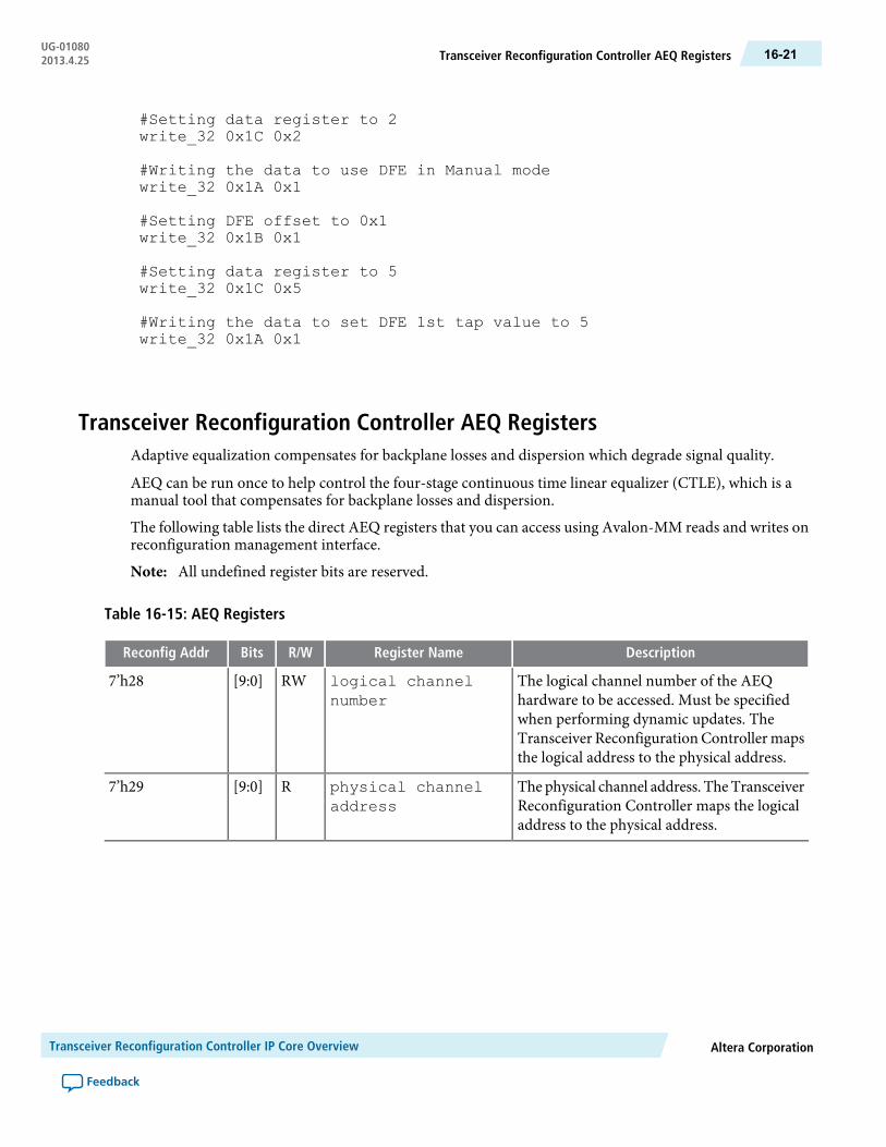
#Setting data register to 2write_32 0x1C 0x2
#Writing the data to use DFE in Manual modewrite_32 0x1A 0x1
#Setting DFE offset to 0x1write_32 0x1B 0x1
#Setting data register to 5write_32 0x1C 0x5
#Writing the data to set DFE 1st tap value to 5write_32 0x1A 0x1
Transceiver Reconfiguration Controller AEQ RegistersAdaptive equalization compensates for backplane losses and dispersion which degrade signal quality.
AEQ can be run once to help control the four-stage continuous time linear equalizer (CTLE), which is amanual tool that compensates for backplane losses and dispersion.
The following table lists the direct AEQ registers that you can access using Avalon-MM reads and writes onreconfiguration management interface.
All undefined register bits are reserved.Note:
Table 16-15: AEQ Registers
DescriptionRegister NameR/WBitsReconfig Addr
The logical channel number of the AEQhardware to be accessed. Must be specifiedwhen performing dynamic updates. TheTransceiver ReconfigurationControllermapsthe logical address to the physical address.
logical channelnumber
RW[9:0]7’h28
The physical channel address. TheTransceiverReconfiguration Controller maps the logicaladdress to the physical address.
physical channeladdress
R[9:0]7’h29
Altera CorporationTransceiver Reconfiguration Controller IP Core Overview
Feedback
16-21Transceiver Reconfiguration Controller AEQ RegistersUG-010802013.4.25

DescriptionRegister NameR/WBitsReconfig Addr
Error.When asserted, indicates an error.This bit is asserted when the channel addressis invalid.
control and status
R[9]
7’h2ABusy. When asserted, indicates that areconfiguration operation is in progress.
R[8]
Read. Writing a 1 to this bit triggers a readoperation.
W[1]
Write. Writing a 1 to this bit triggers a writeoperation.
W[0]
Specifies the address of the AEQ register to beread or written. Refer to Table 16-16 fordetails.
aeq_offsetRW[3:0]7’h2B
Specifies the read or write data.dataRW[15:0]7’h2C
The following table describes the AEQ registers that you can access to change AEQ settings.
All undefined register bits are reserved and must be set to 0.Note:
Table 16-16: AEQ Offsets and Values
DefaultValue
DescriptionRegister NameR/WBitsOffset
1b’0When asserted, indicates that adaptation hascompleted. In One-Time Adaptation Mode, AEQstops searching new EQ settings even if the signalquality of incoming serial data is inadequate.
For some extreme cases, when the channel loss istoo much for AEQ to compensate, the adapt_done signal may never be asserted. The AEQengine can take up to 50,000 reconfiguration clockcycles before selecting the final equalization settings.
adapt_doneR[8]
0x0
2’b00Specifies the following address modes:
• 2’b00: Low power manual equalization mode• 2’b01: One-time AEQ adaptation at power up• 2’b11: Reserved
modeRW[1:0]
Transceiver Reconfiguration Controller IP Core OverviewAltera Corporation
Feedback
UG-01080Transceiver Reconfiguration Controller AEQ Registers16-22 2013.4.25

DefaultValue
DescriptionRegister NameR/WBitsOffset
4’b0000This is the value set by the automatic AEQadaptation performed at startup. If you choose toperform manual equalization using the linearequalizer, you can use this value as a reference.Although automatic and manual equalization donot provide identical functionality, specifying thisvalue enables manual equalization to approximatethe original setting.
equalizationresults
R[3:0]0x1
Refer to Changing Transceiver Settings Using Register-Based Reconfiguration for the procedures you can useto control AEQ.
Transceiver Reconfiguration Controller ATX PLL Calibration RegistersThe ATX PLL Calibration registers allow you to rerun ATX calibration after power up. The TransceiverReconfiguration Controller automatically runs ATX calibration at power up.
You may need to rerun ATX calibration if you reset an ATX PLL and it does not lock after thespecified lock time.
Note:
The following table lists the direct access ATX registers that you can access using Avalon-MM reads andwrites on reconfiguration management interface.
All undefined register bits are reserved.Note:
Table 16-17: ATX Tuning Registers
DescriptionRegister NameR/WBitsATX Addr
The logical channel number. The TransceiverReconfiguration Controller maps the logicaladdress to the physical address.
logical channelnumber
RW[9:0]7’h30
Altera CorporationTransceiver Reconfiguration Controller IP Core Overview
Feedback
16-23Transceiver Reconfiguration Controller ATX PLL Calibration RegistersUG-010802013.4.25
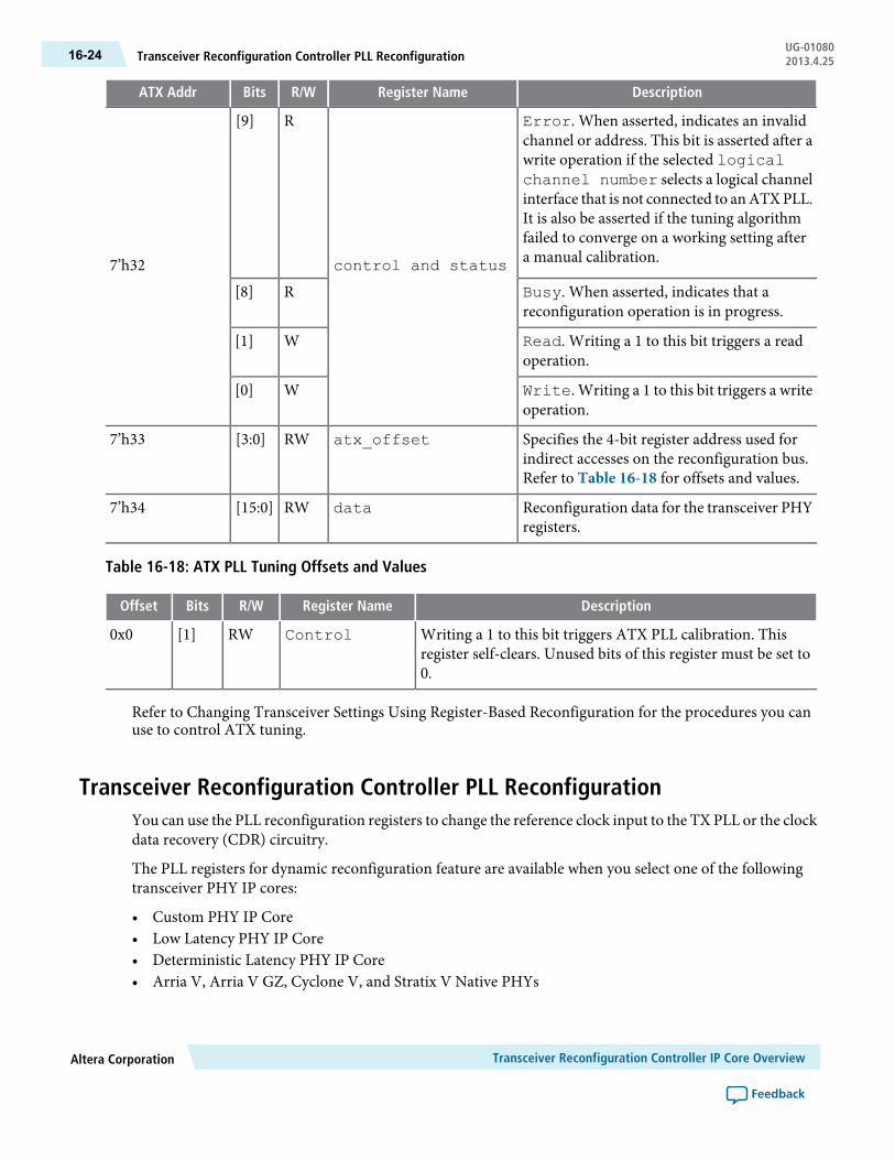
DescriptionRegister NameR/WBitsATX Addr
Error. When asserted, indicates an invalidchannel or address. This bit is asserted after awrite operation if the selected logicalchannel number selects a logical channelinterface that is not connected to anATXPLL.It is also be asserted if the tuning algorithmfailed to converge on a working setting aftera manual calibration.control and status
R[9]
7’h32
Busy. When asserted, indicates that areconfiguration operation is in progress.
R[8]
Read. Writing a 1 to this bit triggers a readoperation.
W[1]
Write. Writing a 1 to this bit triggers a writeoperation.
W[0]
Specifies the 4-bit register address used forindirect accesses on the reconfiguration bus.Refer to Table 16-18 for offsets and values.
atx_offsetRW[3:0]7’h33
Reconfiguration data for the transceiver PHYregisters.
dataRW[15:0]7’h34
Table 16-18: ATX PLL Tuning Offsets and Values
DescriptionRegister NameR/WBitsOffset
Writing a 1 to this bit triggers ATX PLL calibration. Thisregister self-clears. Unused bits of this register must be set to0.
ControlRW[1]0x0
Refer to Changing Transceiver Settings Using Register-Based Reconfiguration for the procedures you canuse to control ATX tuning.
Transceiver Reconfiguration Controller PLL ReconfigurationYou can use the PLL reconfiguration registers to change the reference clock input to the TX PLL or the clockdata recovery (CDR) circuitry.
The PLL registers for dynamic reconfiguration feature are available when you select one of the followingtransceiver PHY IP cores:
• Custom PHY IP Core• Low Latency PHY IP Core• Deterministic Latency PHY IP Core• Arria V, Arria V GZ, Cyclone V, and Stratix V Native PHYs
Transceiver Reconfiguration Controller IP Core OverviewAltera Corporation
Feedback
UG-01080Transceiver Reconfiguration Controller PLL Reconfiguration16-24 2013.4.25

You can establish the number of possible PLL configurations on the Reconfiguration tab of the appropriatetransceiver PHY IP core. The Reconfiguration tab allows you to specify up to five input reference clocksand up to four TX PLLs. You can also change the input clock source to the CDR PLL; up to five input clocksources are possible. If you plan to dynamically reconfigure the PLLs in your design, you must also enableAllow PLL Reconfiguration and specify the Main TX PLL logical index which is the PLL that theQuartus II software instantiates at power up. The following figure illustrates these parameters.
Figure 16-4: Reconfiguration Tab of Custom, Low Latency, and Deterministic Latency Transceiver PHYs
If you dynamically reconfigure PLLs, you must provide your own reset logic by including the AlteraReset Controller IP Core or your own custom reset logic in your design. For more information aboutthe Altera-provided reset controller, refer to Chapter 17, Transceiver PHY Reset Controller IP Core.
Note:
For more information about the Stratix V reset sequence, refer to Transceiver Reset Control in Stratix VDevices in volume 2 of the Stratix VDevice Handbook. For Arria V devices, refer toTransceiver Reset Controland Power-Down in Arria V Devices. For Cyclone V devices refer to Transceiver Reset Control and PowerDown in Cyclone V Devices.
When you specifymultiple PLLs, youmust use theQSF assignment,XCVR_TX_PLL_RECONFIG_GROUP,to identify the PLLs within a reconfiguration group using the Assignment Editor. TheXCVR_TX_PLL_RECONFIG_GROUP assignment identifies PLLs that theQuartus II Fitter canmerge. Youcan assign TX PLLs from different transceiver PHY IP core instances to the same group.
You must create the XCVR_TX_PLL_RECONFIG_GROUP even if one transceiver PHY IP coreinstance instantiates multiple TX PLLs.
Note:
Altera CorporationTransceiver Reconfiguration Controller IP Core Overview
Feedback
16-25Transceiver Reconfiguration Controller PLL ReconfigurationUG-010802013.4.25

Related InformationTransceiver Reset Control in Stratix V Devices
Transceiver Reset Control and Power-Down in Arria V Devices
Transceiver Reset Control and Power Down in Cyclone V Devices
Transceiver Reconfiguration Controller PLL Reconfiguration RegistersLists the PLL reconfiguration registers that you can access using Avalon-MM read and write commands onreconfiguration management interface.
All undefined register bits are reserved.Note:
Table 16-19: PLL Reconfiguration Registers
DescriptionRegister NameR/WBitsReconfig Addr
The logical channel number.Must be specifiedwhen performing dynamic updates. TheTransceiver ReconfigurationControllermapsthe logical address to the physical address.
When reconfiguring the reference clock forthe TX PLL you must specify the PLL's logicalchannel number. When reconfiguring thereference clock for the CDR you must specifythe channel's logical channel number.
logical channelnumber
RW[9:0]7’h40
The physical channel address. TheTransceiverReconfiguration Controller maps the logicaladdress to the physical address.
physical channeladdress
R[9:0]7’h41
When asserted, indicates an error. This bit isasserted if any of the following conditionsoccur:
• The channel address is invalid.• The PHY address is invalid.• The address offset is invalid.
control and status
R[9]
7’h42MIF Busy. When asserted, indicates that areconfiguration operation is in progress.
R[8]
Read. Writing a 1 to this bit triggers a readoperation.
W[1]
Write. Writing a 1 to this bit triggers a writeoperation.
W[0]
Transceiver Reconfiguration Controller IP Core OverviewAltera Corporation
Feedback
UG-01080Transceiver Reconfiguration Controller PLL Reconfiguration Registers16-26 2013.4.25
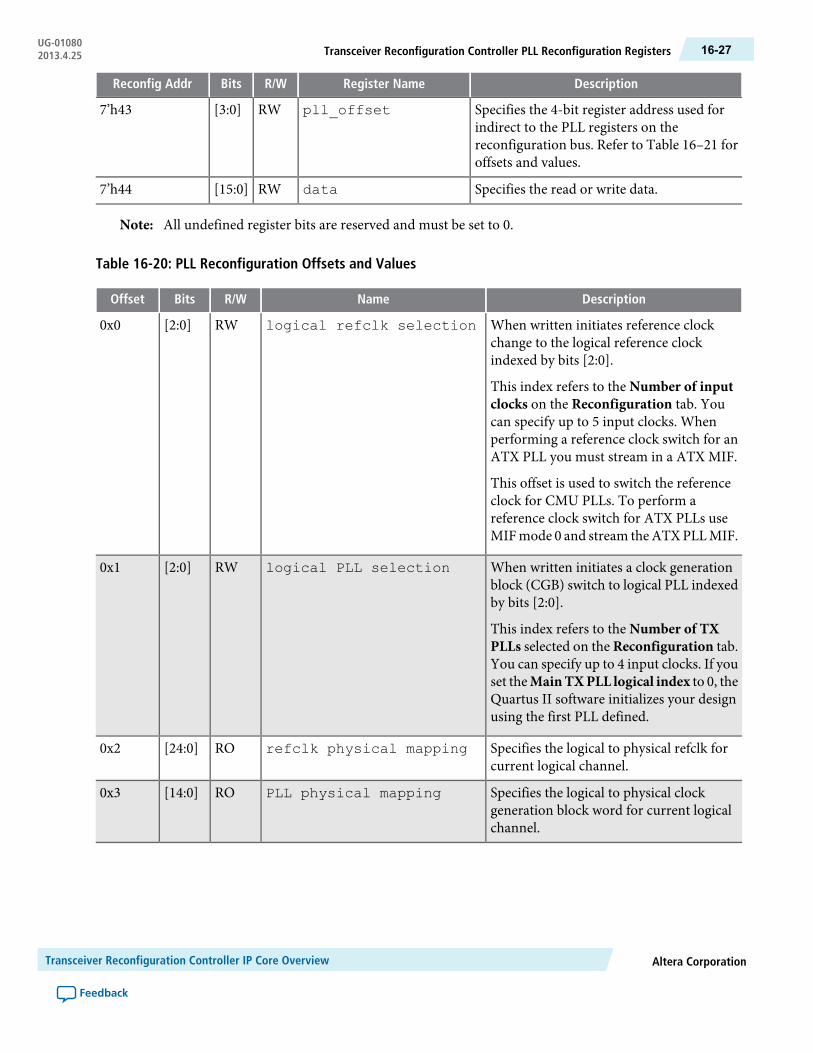
DescriptionRegister NameR/WBitsReconfig Addr
Specifies the 4-bit register address used forindirect to the PLL registers on thereconfiguration bus. Refer to Table 16–21 foroffsets and values.
pll_offsetRW[3:0]7’h43
Specifies the read or write data.dataRW[15:0]7’h44
All undefined register bits are reserved and must be set to 0.Note:
Table 16-20: PLL Reconfiguration Offsets and Values
DescriptionNameR/WBitsOffset
When written initiates reference clockchange to the logical reference clockindexed by bits [2:0].
This index refers to the Number of inputclocks on the Reconfiguration tab. Youcan specify up to 5 input clocks. Whenperforming a reference clock switch for anATX PLL you must stream in a ATX MIF.
This offset is used to switch the referenceclock for CMU PLLs. To perform areference clock switch for ATX PLLs useMIFmode 0 and stream theATXPLLMIF.
logical refclk selectionRW[2:0]0x0
When written initiates a clock generationblock (CGB) switch to logical PLL indexedby bits [2:0].
This index refers to the Number of TXPLLs selected on the Reconfiguration tab.You can specify up to 4 input clocks. If youset theMainTXPLL logical index to 0, theQuartus II software initializes your designusing the first PLL defined.
logical PLL selectionRW[2:0]0x1
Specifies the logical to physical refclk forcurrent logical channel.
refclk physical mappingRO[24:0]0x2
Specifies the logical to physical clockgeneration block word for current logicalchannel.
PLL physical mappingRO[14:0]0x3
Altera CorporationTransceiver Reconfiguration Controller IP Core Overview
Feedback
16-27Transceiver Reconfiguration Controller PLL Reconfiguration RegistersUG-010802013.4.25

Transceiver Reconfiguration Controller DCD Calibration RegistersDCD runs automatically at power up. After power up, you can rerun DCD by writing to the DCD controlregister. Altera recommends that you run DCD calibration for Arria V and Cyclone V devices if the datarate is greater than 4.9152 Gbps.
All undefined register bits are reserved.Note:
Table 16-21: DCD Registers
DescriptionRegister NameR/WBitsReconfig Addr
The logical channel number.Must be specifiedwhen performing dynamic updates. TheTransceiver ReconfigurationControllermapsthe logical address to the physical address.
logical channelnumber
RW[9:0]7’h48
The physical channel address. TheTransceiverReconfiguration Controller maps the logicaladdress to the physical address.
physical channeladdress
R[9:0]7’h49
Specifies the offset of the DCD setting to bereconfigured. Table 16-22 describes the validoffset values.
dcd offsetRW[6:0]7’h4B
Reconfiguration data for the PMA analogsettings.
dcd_dataRW[6:0]7’h4C
All undefined register bits are reserved and must be set to 0.Note:
Table 16-22: DCD Offsets and Values
DescriptionRegister NameR/WBitsOffset
Writing 1'b1 to this bit tomanually triggersDCD calibration.
dcd_controlRW[5:0]0x0
Transceiver Reconfiguration Controller Channel and PLL ReconfigurationYou can use channel and PLL reconfiguration to dynamically reconfigure the channel and PLL settings ina transceiver PHY IP core.
Among the settings that you can change dynamically are the data rate and interface width. Refer to DeviceSupport for Dynamic Reconfiguration for specific information about reconfiguration in Arria V, Cyclone V,and Stratix V devices.
TheTransceiver ReconfigurationController’s StreamerModule implements channel andPLL reconfiguration.Refer to the Streamer Module Registers for more information about this module.
Transceiver Reconfiguration Controller IP Core OverviewAltera Corporation
Feedback
UG-01080Transceiver Reconfiguration Controller DCD Calibration Registers16-28 2013.4.25
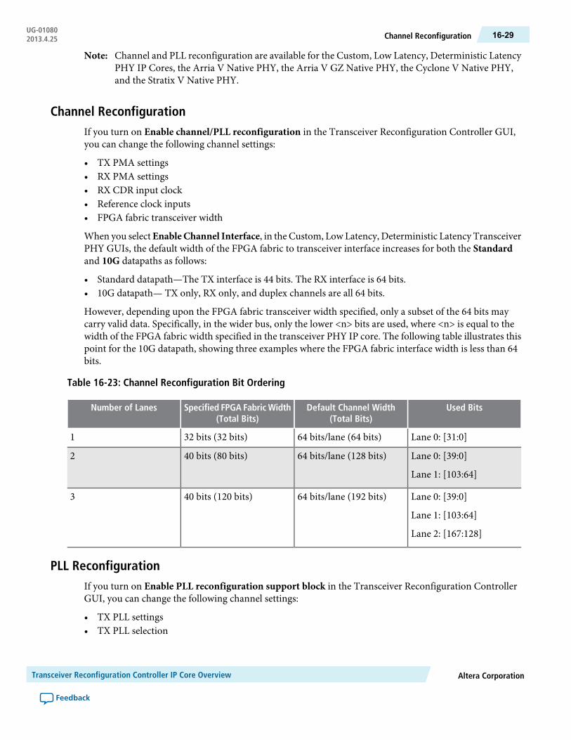
Channel and PLL reconfiguration are available for the Custom, Low Latency, Deterministic LatencyPHY IP Cores, the Arria V Native PHY, the Arria V GZ Native PHY, the Cyclone V Native PHY,and the Stratix V Native PHY.
Note:
Channel ReconfigurationIf you turn on Enable channel/PLL reconfiguration in the Transceiver Reconfiguration Controller GUI,you can change the following channel settings:
• TX PMA settings• RX PMA settings• RX CDR input clock• Reference clock inputs• FPGA fabric transceiver width
When you selectEnableChannel Interface, in the Custom, Low Latency, Deterministic Latency TransceiverPHY GUIs, the default width of the FPGA fabric to transceiver interface increases for both the Standardand 10G datapaths as follows:
• Standard datapath—The TX interface is 44 bits. The RX interface is 64 bits.• 10G datapath— TX only, RX only, and duplex channels are all 64 bits.
However, depending upon the FPGA fabric transceiver width specified, only a subset of the 64 bits maycarry valid data. Specifically, in the wider bus, only the lower <n> bits are used, where <n> is equal to thewidth of the FPGA fabric width specified in the transceiver PHY IP core. The following table illustrates thispoint for the 10G datapath, showing three examples where the FPGA fabric interface width is less than 64bits.
Table 16-23: Channel Reconfiguration Bit Ordering
Used BitsDefault Channel Width(Total Bits)
Specified FPGA Fabric Width(Total Bits)
Number of Lanes
Lane 0: [31:0]64 bits/lane (64 bits)32 bits (32 bits)1
Lane 0: [39:0]
Lane 1: [103:64]
64 bits/lane (128 bits)40 bits (80 bits)2
Lane 0: [39:0]
Lane 1: [103:64]
Lane 2: [167:128]
64 bits/lane (192 bits)40 bits (120 bits)3
PLL ReconfigurationIf you turn on Enable PLL reconfiguration support block in the Transceiver Reconfiguration ControllerGUI, you can change the following channel settings:
• TX PLL settings• TX PLL selection
Altera CorporationTransceiver Reconfiguration Controller IP Core Overview
Feedback
16-29Channel ReconfigurationUG-010802013.4.25
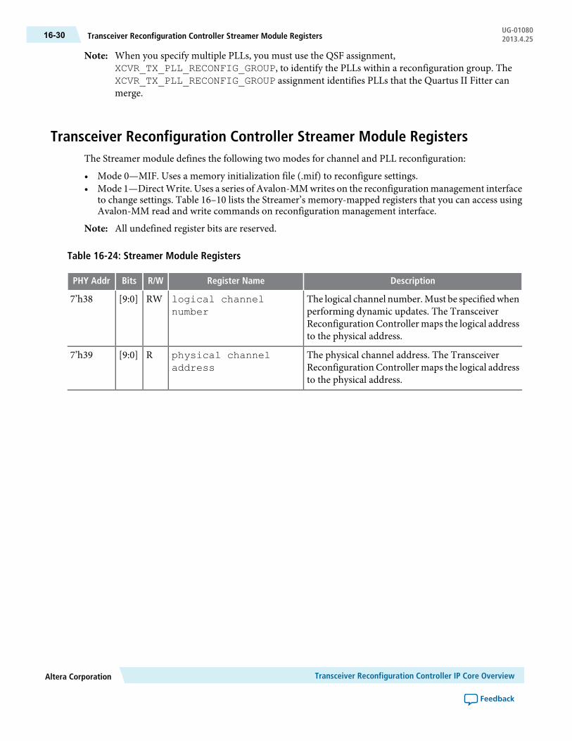
When you specify multiple PLLs, you must use the QSF assignment,XCVR_TX_PLL_RECONFIG_GROUP, to identify the PLLs within a reconfiguration group. The
Note:
XCVR_TX_PLL_RECONFIG_GROUP assignment identifies PLLs that the Quartus II Fitter canmerge.
Transceiver Reconfiguration Controller Streamer Module RegistersThe Streamer module defines the following two modes for channel and PLL reconfiguration:
• Mode 0—MIF. Uses a memory initialization file (.mif) to reconfigure settings.• Mode 1—Direct Write. Uses a series of Avalon-MM writes on the reconfiguration management interface
to change settings. Table 16–10 lists the Streamer’s memory-mapped registers that you can access usingAvalon-MM read and write commands on reconfiguration management interface.
All undefined register bits are reserved.Note:
Table 16-24: Streamer Module Registers
DescriptionRegister NameR/WBitsPHY Addr
The logical channel number.Must be specifiedwhenperforming dynamic updates. The TransceiverReconfiguration Controller maps the logical addressto the physical address.
logical channelnumber
RW[9:0]7’h38
The physical channel address. The TransceiverReconfiguration Controller maps the logical addressto the physical address.
physical channeladdress
R[9:0]7’h39
Transceiver Reconfiguration Controller IP Core OverviewAltera Corporation
Feedback
UG-01080Transceiver Reconfiguration Controller Streamer Module Registers16-30 2013.4.25
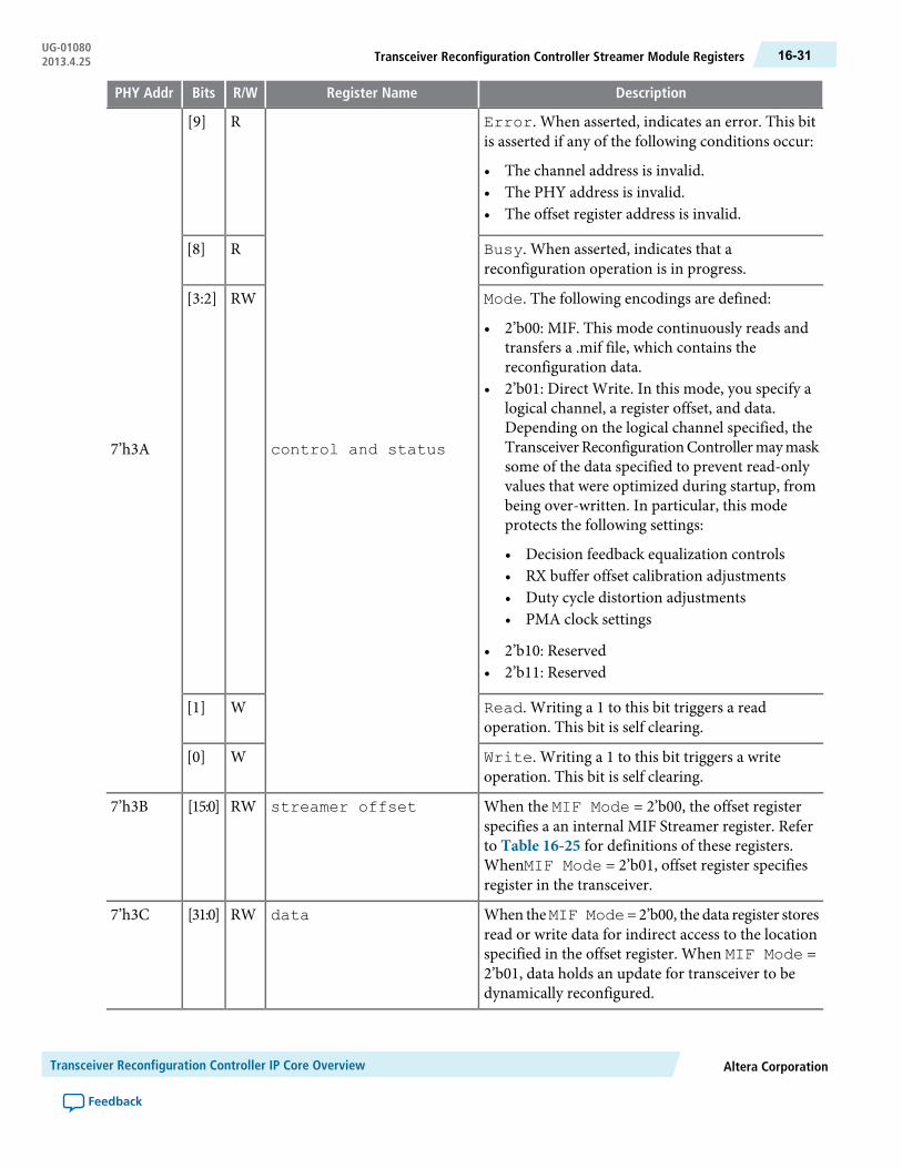
DescriptionRegister NameR/WBitsPHY Addr
Error. When asserted, indicates an error. This bitis asserted if any of the following conditions occur:
• The channel address is invalid.• The PHY address is invalid.• The offset register address is invalid.
control and status
R[9]
7’h3A
Busy. When asserted, indicates that areconfiguration operation is in progress.
R[8]
Mode. The following encodings are defined:
• 2’b00: MIF. This mode continuously reads andtransfers a .mif file, which contains thereconfiguration data.
• 2’b01: Direct Write. In this mode, you specify alogical channel, a register offset, and data.Depending on the logical channel specified, theTransceiverReconfigurationControllermaymasksome of the data specified to prevent read-onlyvalues that were optimized during startup, frombeing over-written. In particular, this modeprotects the following settings:
• Decision feedback equalization controls• RX buffer offset calibration adjustments• Duty cycle distortion adjustments• PMA clock settings
• 2’b10: Reserved• 2’b11: Reserved
RW[3:2]
Read. Writing a 1 to this bit triggers a readoperation. This bit is self clearing.
W[1]
Write. Writing a 1 to this bit triggers a writeoperation. This bit is self clearing.
W[0]
When the MIF Mode = 2’b00, the offset registerspecifies a an internal MIF Streamer register. Referto Table 16-25 for definitions of these registers.WhenMIF Mode = 2’b01, offset register specifiesregister in the transceiver.
streamer offsetRW[15:0]7’h3B
When theMIF Mode=2’b00, the data register storesread or write data for indirect access to the locationspecified in the offset register. When MIF Mode =2’b01, data holds an update for transceiver to bedynamically reconfigured.
dataRW[31:0]7’h3C
Altera CorporationTransceiver Reconfiguration Controller IP Core Overview
Feedback
16-31Transceiver Reconfiguration Controller Streamer Module RegistersUG-010802013.4.25
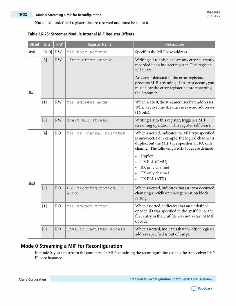
All undefined register bits are reserved and must be set to 0.Note:
Table 16-25: Streamer Module Internal MIF Register Offsets
DescriptionRegister NameR/WBitsOffset
Specifies the MIF base address.MIF base addressRW[31:0]0x0
Writing a 1 to this bit clears any error currentlyrecorded in an indirect register. This registerself clears.
Any error detected in the error registersprevents MIF streaming. If an error occurs, youmust clear the error register before restartingthe Streamer.
Clear error statusRW[2]
0x1
When set to 0, the streamer uses byte addresses.When set to 1, the streamer uses word addresses(16 bits).
MIF address modeRW[1]
Writing a 1 to this register, triggers a MIFstreaming operation. This register self clears.
Start MIF streamRW[0]
When asserted, indicates theMIF type specifiedis incorrect. For example, the logical channel isduplex, but the MIF type specifies an RX onlychannel. The following 5MIF types are defined:
• Duplex• TX PLL (CMU)• RX only channel• TX only channel• TX PLL (ATX)
MIF or Channel mismatchRO[4]
0x2When asserted, indicates that an error occurredchanging a refclk or clock generation blocksetting.
PLL reconfiguration IPerror
RO[2]
When asserted, indicates that an undefinedopcode ID was specified in the .mif file, or thefirst entry in the .mif file was not a start of MIFopcode.
MIF opcode errorRO[1]
When asserted, indicates that the offset registeraddress specified is out of range.
Invalid register accessRO[0]
Mode 0 Streaming a MIF for ReconfigurationIn mode 0, you can stream the contents of a MIF containing the reconfiguration data to the transceiver PHYIP core instance.
Transceiver Reconfiguration Controller IP Core OverviewAltera Corporation
Feedback
UG-01080Mode 0 Streaming a MIF for Reconfiguration16-32 2013.4.25

You specify this mode by writing a value of 2'b00 into bits 2 and 3 of the control and status register, asindicated in Streamer Module Registers. Mode 0 simplifies the reconfiguration process because allreconfiguration data is stored in the MIF, which is streamed to the transceiver PHY IP in a single step.
The MIF can change PLL settings, reference clock inputs, or the TX PLL selection. After the MIF streamingupdate is complete, all transceiver PHY IP core settings reflect the value specified by the MIF. Refer toStreamer-Based Reconfiguration for an example of a MIF update.
Mode 1 Avalon-MM Direct Writes for ReconfigurationThis section describes mode 1 Avalon-MM direct writes for reconfiguration.
You specify this mode by writing a value of 2'b01 into bits 2 and 3 of the control and status register, asindicated in Streamer Module Registers. In this mode, you can write directly to transceiver PHY IP coreregisters to perform reconfiguration. Refer to “Direct Write Reconfiguration” for an example of an updateusing mode 1. In mode 1, you can selectively reconfigure portions of the transceiver PHY IP core. Unlikemode 0, mode 1 allows you to write only the data required for a reconfiguration.
MIF GenerationTheMIF stores the configuration data for the transceiver PHY IP cores. TheQuartus II software automaticallygenerates MIFs after each successful compilation.
MIFs are stored in the reconfig_mif folder of the project's working directly. This folder stores all MIFsassociated with the compiled project for each transceiver PHY IP core instance in the design. The parametersettings of PHY IP core instance reflect the currently specified MIF. You can store the MIF in an on-chipROM or any other type of memory. This memory must connect to the MIF reconfiguration managementinterface.
The following example shows file names for the .mif files for a designwith two channels. This design exampleincludes two transceiver PHY IP core instances running at different data rates. Both transceiver PHY IPcore instances have two TX PLLs specified to support both 1 Gbps and 2.5 Gbps data rates. The Quartus IIsoftware generates two TX PLL .mif files for each PLL. The difference between the .mif files is the PLLreference clock specified. To dynamically reconfigure the channel from the initially specified data rate to anew data rate, you can use the MIF streaming function to load the other .mif.
When reconfiguration is limited to a few settings, you can create a partial .mif that only includes thesettings that must be updated. Refer to Reduced MIF Creation for more information about creatinga partial .mif file.
Note:
Example 16-4: Quartus II Generated MIF Files
<project_dir>/reconfig_mif/inst0_1g_channel.mif
<project_dir>/reconfig_mif/inst0_1g_txpll0.mif
<project_dir>/reconfig_mif/inst0_1g_txpll1.mif
<project_dir>/reconfig_mif/inst0_2p5g_channel.mif
<project_dir>/reconfig_mif/inst0_2p5g_txpll0.mif
<project_dir>/reconfig_mif/inst0_2p5g_txpll1.mif
Altera CorporationTransceiver Reconfiguration Controller IP Core Overview
Feedback
16-33Mode 1 Avalon-MM Direct Writes for ReconfigurationUG-010802013.4.25

Creating MIFs for Designs that Include Bonded or GT ChannelsYou can generate MIF files for projects that include bonded or GT channels using the following procedure:
1. Create separate 1-channel designs for each frequency TX PLL frequency that your actual design requires.2. Compile each design with the Quartus II software.3. Save the MIF files that Quartus II software generates.4. Use the MIF files that you have created from your 1-channel designs for reconfiguration in your design
that includes bonded clocks.
The Quartus II software automatically generates MIF for all designs that support POF generation with thefollowing exceptions:
• Designs that use bonded channels so that the same TX PLL output drives several channels• GT channels• Non-bonded channels in a design that also includes bonded channels
MIF FormatThe MIF file is organized into records where each record contains the information necessary to carry outthe reconfiguration process.
There are two types of records: non-data records and data records. A MIF can contain a variable number ofrecords, depending on the target transceiver channel. Both data records and non-data records are 16-bitslong.
For both record types the high-order 5 bits represent the length field. A length field of 5’b0, indicatesa non-data record which contains an opcode. A length field that is not zero indicates a data record.
For a non-data record, the opcode is represented by the lower 5-bits in the record.
Table 16-26: Opcodes for MIF Files
Opcode DescriptionOpcode
Reserved5’b00000
Start of MIF5’b00001
Channel format indicator specifying the MIF channeltype. The following encodings are defined:
• 3’b000: Duplex channel• 3’b001: TX PLL (CMU)• 3’b010: RX only channel• 3’b011: TX only channel• 3’b100: TX PLL (ATX)
5’b00010
Reference Clock switch5’b00011
CGB switch5’b00100
Reserved5’b00101-5’b11110
Transceiver Reconfiguration Controller IP Core OverviewAltera Corporation
Feedback
UG-01080Creating MIFs for Designs that Include Bonded or GT Channels16-34 2013.4.25
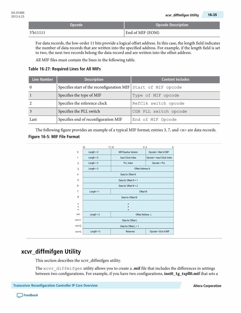
Opcode DescriptionOpcode
End of MIF (EOM)5’b11111
For data records, the low-order 11 bits provide a logical offset address. In this case, the length field indicatesthe number of data records that are written into the specified address. For example, if the length field is setto two, the next two records belong the data record and are written into the offset address.
All MIF files must contain the lines in the following table.
Table 16-27: Required Lines for All MIFs
Content IncludesDescriptionLine Number
Start of MIF opcodeSpecifies start of the reconfiguration MIF0
Type of MIF opcodeSpecifies the type of MIF1
RefClk switch opcodeSpecifies the reference clock2
CGB PLL switch opcodeSpecifies the PLL switch3
End of MIF OpcodeSpecifies end of reconfiguration MIFLast
The following figure provides an example of a typical MIF format; entries 3, 7, and <n> are data records.Figure 16-5: MIF File Format
Length = 00
1
2
3
4
5
6
7
8
<n>
<n>+1
<n>+2
<n>+3
MIF/Quartus Version Opcode = Start of MIF
Length = 0 Input Clock Index Opcode = Input Clock Index
Length = 0 PLL Index Opcode = PLL
Length = 0 Reserved Opcode = End of MIF
Length = 3 Offset Address N
Data for Offset N
Length = 1 Offset M
Data for Offset M
Data for Offset N + 1
Data for Offset N + 2
Length = 2 Offset Address L
Data for Offset L
Data for Offset L + 1
15 11 10
......
5 04
xcvr_diffmifgen UtilityThis section describes the xcvr_diffmifgen utility.
The xcvr_diffmifgen utility allows you to create a .mif file that includes the differences in settingsbetween two configurations. For example, if you have two configurations, inst0_1g_txpll0.mif that sets a
Altera CorporationTransceiver Reconfiguration Controller IP Core Overview
Feedback
16-35xcvr_diffmifgen UtilityUG-010802013.4.25

TX PLL0 bandwidth to 1 Gbps and inst0_5g_txpll0.mif that sets the TX PLL0 bandwidth to 5 Gbps, thexcvr_diffmifgen utility creates to_inst0_1g_txpll0.mif and to_inst0_5g_txpll0.mif that include theinformation necessary to change from 1 Gbps to 5 Gbps and from 5 Gbps to 1 Gbps. You can use these filesto reduce reconfiguration and simulation times.
The xcvr_diffmifgen utility can operate on up to five MIF files. This utility only works on MIF filesat the same revision level. If you try to compare MIF files that are not at the same revision level,xcvr_diffmifgen issues a warning.
You can also use the Reduced MIF Creation to create reduced MIF files.Note:
Example 16-5: xcvr_diffmifgen
xcvr_diffmifgen <options> <MIF file 1> <MIF file 2> <Mif file n>
Arguments:-h: Displays help-noopt: The output file is not optimized
The format of the reduced MIF file is the same as for the original MIF files as described in MIF Format. Thereduced MIF file, preserves the lines shown in the following table:
Table 16-28: Required Lines for All MIFs
Content IncludesDescriptionLine Number
Start of MIF opcodeSpecifies start of the reconfiguration MIF0
Type of MIF opcodeSpecifies the type of MIF1
RefClk switch opcodeSpecifies the reference clock2
CGB PLL switch opcodeSpecifies the PLL switch3
End of MIF OpcodeSpecifies end of reconfiguration MIFLast
For each difference between the files compared, the reduced MIF file includes the following two records:
1. A record indicating the length and address of the change.2. The changed data.
The following example shows part of two MIF files, MIF_A and MIF_B. Line 6, 16, and 20 are different.
Transceiver Reconfiguration Controller IP Core OverviewAltera Corporation
Feedback
UG-01080xcvr_diffmifgen Utility16-36 2013.4.25

Example 16-6: Two Partial MIF files
The following example shows and the reduced MIF file, to_MIF_A created by the xcvr_diffmifgen utility:
Example 16-7: Reduced MIF File to_MIF_A
The xcvr_diffmif utility only works for Quartus II post-fit simulation and hardware.Note:
Altera CorporationTransceiver Reconfiguration Controller IP Core Overview
Feedback
16-37xcvr_diffmifgen UtilityUG-010802013.4.25
Reduced MIF CreationThe procedure described here is an alternative way to generate a reduced MIF file. You can also use thexcvr_diffmifgen Utility. Follow these steps to generate a reduced MIF:
1. Determine the content differences between the originalMIF and the reconfiguredMIF. For this example,assume there are bit differences at offset 5 and offset 20. These offsets reside in the PMA-TX andPMA-RXsections of the MIF.
2. Use a text editor to create a new reduced MIF file. In this example, we will call the reduced MIFreduced_mif.mif. Copy theWIDTH,DEPTH,ADDRESS_RADIX,DATA_RADIX andCONTENT BEGINlines from the original MIF to reduced_mif.mif.
3. Copy offsets 0-3 as describedTable 16-28 from the originalMIF to reduced_mif.mif. The reconfigurationMIF must always include these lines.
4. Copy all offsets of the PMA-TX and PMA-RX sections from the reconfigured MIF to reduced_mif.mif.5. Copy the End of MIF opcode offset and END; from the original MIF to reduced_mif.mif.6. Renumber reduced_mif.mif sequentially and update the DEPTH variable with the new value. The new
value equals the number offsets in reduced_mif.mif.
You can now use reduced_mif.mif to reconfigure the transceiver.
You can create a reduced MIF from the following two MIFs:
• Original MIF—contains the transceiver settings that were specified during the initial compilation• ReconfiguredMIF—contains the new transceiver settings. You generate the reconfiguredMIFbymodifying
the original transceiver settings. For example, if the original compilation specifies a clock divider valueof 1 and the reconfigured compilation specifies a clock divider value of 2, theMIF files reflect that change.The reduced MIF contains only the changed content. In this example, the difference between the twoMIFs would be the clock divider value.
Changing Transceiver Settings Using Register-Based ReconfigurationThis section describes changing the transceiver settings.
In register-based mode, you use a sequence of Avalon-MM writes and reads to update individual transceiversettings. The following section describes how to perform a register-based reconfiguration read and write.
Register-Based WriteComplete the following steps to perform a register-based write:
1. Read the control and status register busy bit (bit 8) until it is clear.2. Write the logical channel number of the channel to be updated to the logical channel number
register.3. Write the <feature> offset address.4. Write the appropriate data value to the data register.5. Write the control and status register write bit to 1’b1.6. Read the control and status register busy bit. Continue to read the busy bit while its value is
one.7. When busy = 0, the Transceiver Reconfiguration Controller has updated the logical channel specified
in Step 2 with the data specified in Step 3.
Transceiver Reconfiguration Controller IP Core OverviewAltera Corporation
Feedback
UG-01080Reduced MIF Creation16-38 2013.4.25

Example 16-8: Register-Based Write of Logical Channel 0 VOD Setting
#Setting logical channel 0write_32 0x8 0x0
#Setting offset to VODwrite_32 0xB 0x0
#Setting data register to 40write_32 0xC 0x28
#Writing all datawrite_32 0xA 0x1Ā
Register-Based ReadComplete the following steps for a read:
1. Read the control and status register busy bit (bit 8) until it is clear.2. Write the logical channel number of the channel to be read to the logical channel number
register.3. Write the <feature> offset address.4. Write the control and status register read bit to 1’b1.5. Read the control and status register busy bit. Continue to read the busy until the value is zero.6. Read the data register to get the data.
Example 16-9: Register-Based Read of Logical Channel 2 Pre-Emphasis Pretap Setting
#Setting logical channel 2write_32 0x8 0x2
#Setting offset to pre-emphasis pretapwrite_32 0xB 0x1
#Writing the logical channel and offset for pre-emphasis pretapwrite_32 0xA 0x2
#Reading data register for the pre-emphasis pretap valueread_32 0xC
Changing Transceiver Settings Using Streamer-Based ReconfigurationThe Streamer’s registers allow you to change to the PCS datapath settings, clock settings, and PLL parametersby reading the new settings from an on- or off-chip ROM.
Altera CorporationTransceiver Reconfiguration Controller IP Core Overview
Feedback
16-39Register-Based ReadUG-010802013.4.25
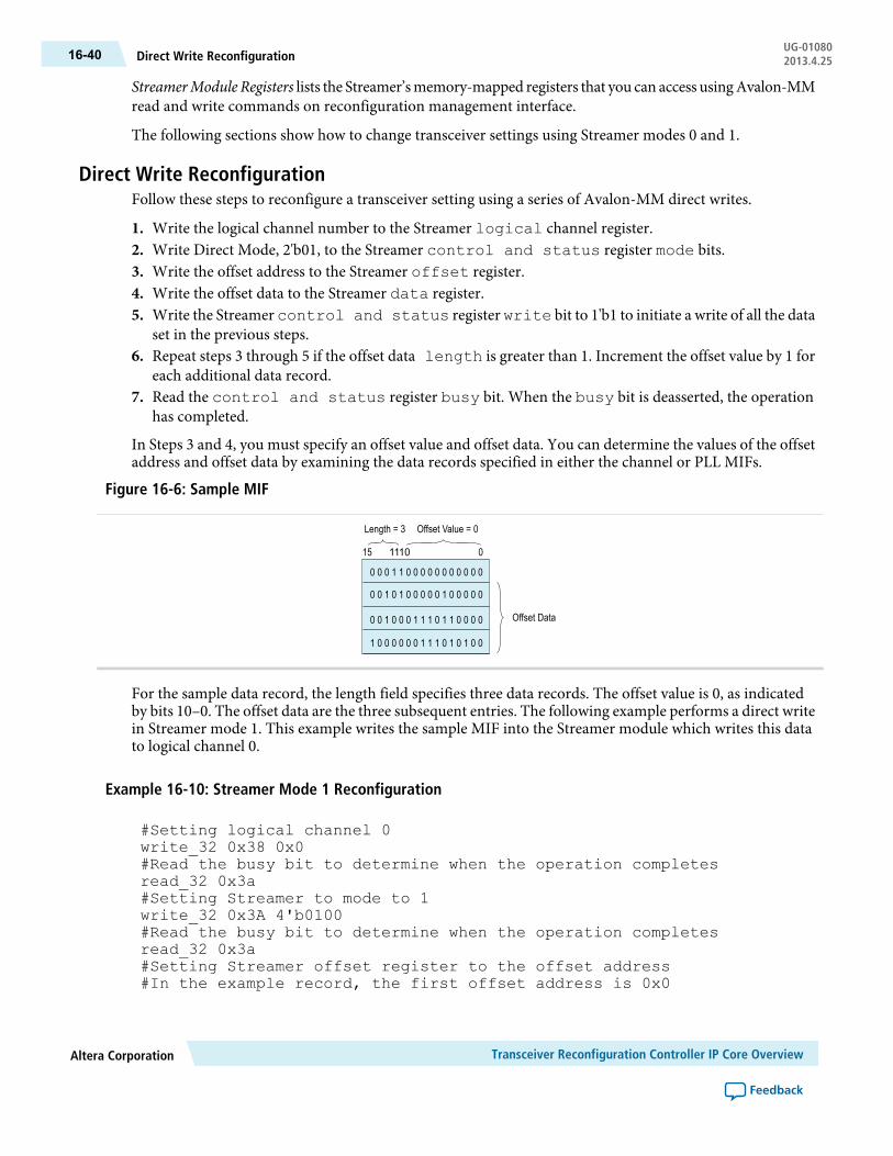
StreamerModule Registers lists the Streamer’smemory-mapped registers that you can access usingAvalon-MMread and write commands on reconfiguration management interface.
The following sections show how to change transceiver settings using Streamer modes 0 and 1.
Direct Write ReconfigurationFollow these steps to reconfigure a transceiver setting using a series of Avalon-MM direct writes.
1. Write the logical channel number to the Streamer logical channel register.2. Write Direct Mode, 2'b01, to the Streamer control and status register mode bits.3. Write the offset address to the Streamer offset register.4. Write the offset data to the Streamer data register.5. Write the Streamer control and status register write bit to 1'b1 to initiate a write of all the data
set in the previous steps.6. Repeat steps 3 through 5 if the offset data length is greater than 1. Increment the offset value by 1 for
each additional data record.7. Read the control and status register busy bit. When the busy bit is deasserted, the operation
has completed.
In Steps 3 and 4, you must specify an offset value and offset data. You can determine the values of the offsetaddress and offset data by examining the data records specified in either the channel or PLL MIFs.
Figure 16-6: Sample MIF
0 0 0 1 1 0 0 0 0 0 0 0 0 0 0 0
0 0 1 0 1 0 0 0 0 0 1 0 0 0 0 0
0 0 1 0 0 0 1 1 1 0 1 1 0 0 0 0
1 0 0 0 0 0 0 1 1 1 0 1 0 1 0 0
Length = 3 Offset Value = 0
Offset Data
15 1110 0
For the sample data record, the length field specifies three data records. The offset value is 0, as indicatedby bits 10–0. The offset data are the three subsequent entries. The following example performs a direct writein Streamer mode 1. This example writes the sample MIF into the Streamer module which writes this datato logical channel 0.
Example 16-10: Streamer Mode 1 Reconfiguration
#Setting logical channel 0write_32 0x38 0x0#Read the busy bit to determine when the operation completesread_32 0x3a#Setting Streamer to mode to 1write_32 0x3A 4'b0100#Read the busy bit to determine when the operation completesread_32 0x3a#Setting Streamer offset register to the offset address#In the example record, the first offset address is 0x0
Transceiver Reconfiguration Controller IP Core OverviewAltera Corporation
Feedback
UG-01080Direct Write Reconfiguration16-40 2013.4.25

write_32 0x3B 0x0#Read the busy bit to determine when the operation completesread_32 0x3a#Setting data register with the first data recordwrite_32 0x3C 16'b0010100000100000#Read the busy bit to determine when the operation completesread_32 0x3a#Writing first data to the Streamerwrite_32 0x3A 0x5#Read the busy bit to determine when the operation completesread_32 0x3a#Incrementing Streamer offset register offset addresswrite_32 0x3B 0x1#Read the busy bit to determine when the operation completesread_32 0x3a#Setting data register with the second data recordwrite_32 0x3C 16'b0010001110110000#Read the busy bit to determine when the operation completesread_32 0x3a#Writing second data to the Streamerwrite_32 0x3A 0x5#Read the busy bit to determine when the operation completesread_32 0x3a#Incrementing Streamer offset register offset addresswrite_32 0x3B 0x2#Read the busy bit to determine when the operation completesread_32 0x3a#Setting data register with the third data recordwrite_32 0x3C 16'b1000000111010100#Read the busy bit to determine when the operation completesread_32 0x3a#Writing third data record to the Streamerwrite_32 0x3A 0x5#Read the busy bit to determine when the operation completesread_32 0x3a#Read the busy bit to determine when the operation completesread_32 0x3a
Streamer-Based ReconfigurationFollow these steps to reconfigure a transceiver setting by streaming the contents of a MIF file through theStreamer Module.
1. Write the logical channel number to the Streamer logical channel register.2. Write MIF mode, 2’b00, to the Streamer control and status register mode bits.3. Write the MIF base address, 0x0, to the Streamer offset register.4. Write the base address of the MIF file to the Streamer data register.5. Write the Streamer control and status register write bit to 1'b1 to initiate a write of all the data
set in the previous steps.6. Write to the Streamer offset register with the value to start a MIF stream, 0x1.
Altera CorporationTransceiver Reconfiguration Controller IP Core Overview
Feedback
16-41Streamer-Based ReconfigurationUG-010802013.4.25
7. Write the Streamer internal data register with the value 0x3 to setup the streaming of the MIF.8. Write to the Streamer control and status register to 1'b1, to initiate the streaming operation.9. Read the control and status register busy bit. When the busy bit is deasserted, the MIF
streaming operation has completed.
The following example illustrates the reconfiguration of logical channel 0 using a MIF with a base addressof 0x100.
Example 16-11: Reconfiguration of Logical Channel 0 Using a MIF
#Setting logical channel 0write_32 0x38 0x0#Setting Streamer mode to 0write_32 0x3A 0x0#Setting Streamer offset register to the MIF base address (0x0)write_32 0x3B 0x0#Setting data register with the MIF base addresswrite_32 0x3C 0x100#Writing all data to the Streamerwrite_32 0x3A 0x1#Setting Streamer Module offset for Start MIF streamwrite_32 0x3B 0x1#Setting data register with 0x3 to setup for streamingwrite_32 0x3C 0x3#Writing all data to the Streamer to start streaming the MIFwrite_32 0x3A 0x1#Read the busy bit to determine when the write has completedread_32 0x3A
Understanding Logical Channel NumberingThis discussion of channel numbering, uses the following definitions:
• Reconfiguration interface—A bundle of signals that connect the Transceiver Reconfiguration Controllerto a transceiver PHY data channel or TX PLL.
• Logical channels—An abstract representation of a channel or TX PLL that does not include physicallocation information.
• Bonded channel—A channel that shares a clock source with at least one other channel.• Physical channel—The physical channel associated with a logical channel.
The following figure illustrates the connections between the Transceiver Reconfiguration Controller and atransceiver bank after running the Quartus II Fitter.
Transceiver Reconfiguration Controller IP Core OverviewAltera Corporation
Feedback
UG-01080Understanding Logical Channel Numbering16-42 2013.4.25

Figure 16-7: Post-Fit Connectivity
TransceiverReconfiguration
Controller
Transceiver Bank
3 Channels
3 Channels
Channel 2Channel 1Channel 0
Channel 3
Channel 5
Channel 4
S M
to EmbeddedProcessor
Reconfig toand from
Transceiver
Stratix V GX, GS, or GT Device
S
S
The transceiver PHY IP cores create a separate reconfiguration interface for each channel and each TX PLL.Each transceiver PHY IP core reports the number of reconfiguration interfaces it requires in the messagepane of its GUI. You must take note of this number so that you can enter it as a parameter in the TransceiverReconfiguration Controller.
The following figure shows the Low Latency PHY IP ore GUI specifying 32 channels. The message paneindicates that reconfiguration interfaces 0–31 are for the transceiver channels and reconfiguration interfaces32–63 are for the TX PLLs.
Figure 16-8: Low Latency Transceiver PHY Example
After Quartus II compilation, many of the interfaces are merged.Note:
Altera CorporationTransceiver Reconfiguration Controller IP Core Overview
Feedback
16-43Understanding Logical Channel NumberingUG-010802013.4.25

The following figure illustrates the GUI for the Transceiver Reconfiguration Controller. To connect the LowLatency PHY IPCore instance to the Transceiver ReconfigurationController, youwould enter 64 forNumberof reconfiguration interfaces. You would not need to enter any values for theOptional interface groupingparameter because all of the interfaces belong to the same transceiver PHY IP core instance.
Figure 16-9: Transceiver Reconfiguration Controller Interface Bundles
The following figure shows a design with two transceiver PHY IP core instances, each with four channels.For this design you would enter 16 for the Number of reconfiguration interfaces and 8, 8 for the Optionalinterface grouping parameter.
Depending upon the transceiver PHY IP core and the parameters specified, the number of reconfigurationinterfaces varies. For a single-channel, RX-only transceiver instance, there is a single reconfiguration interface.One reconfiguration interface is created for a single-channel Low Latency PHY setup as a RX only channel.Two reconfiguration interfaces are created for a single-channel Custom PHY setup as a duplex channel. Thereconfiguration interfaces do not appear as separate buses, but as a single bus of concatenated reconfigurationinterfaces, that grows linearly with the number of reconfiguration interfaces.
Although you must create a separate logical reconfiguration interface for each PHY IP core instance, whenthe Quartus II software compiles your design, it reduces original number of logical interfaces by mergingthem. Allowing the Quartus II software to merge reconfiguration interfaces gives the Fitter more flexibilityin placing transceiver channels. However, the logical channel number remains the same.
You cannot use SignalTap™ to observe the reconfiguration interfaces.Note:
Transceiver Reconfiguration Controller IP Core OverviewAltera Corporation
Feedback
UG-01080Understanding Logical Channel Numbering16-44 2013.4.25
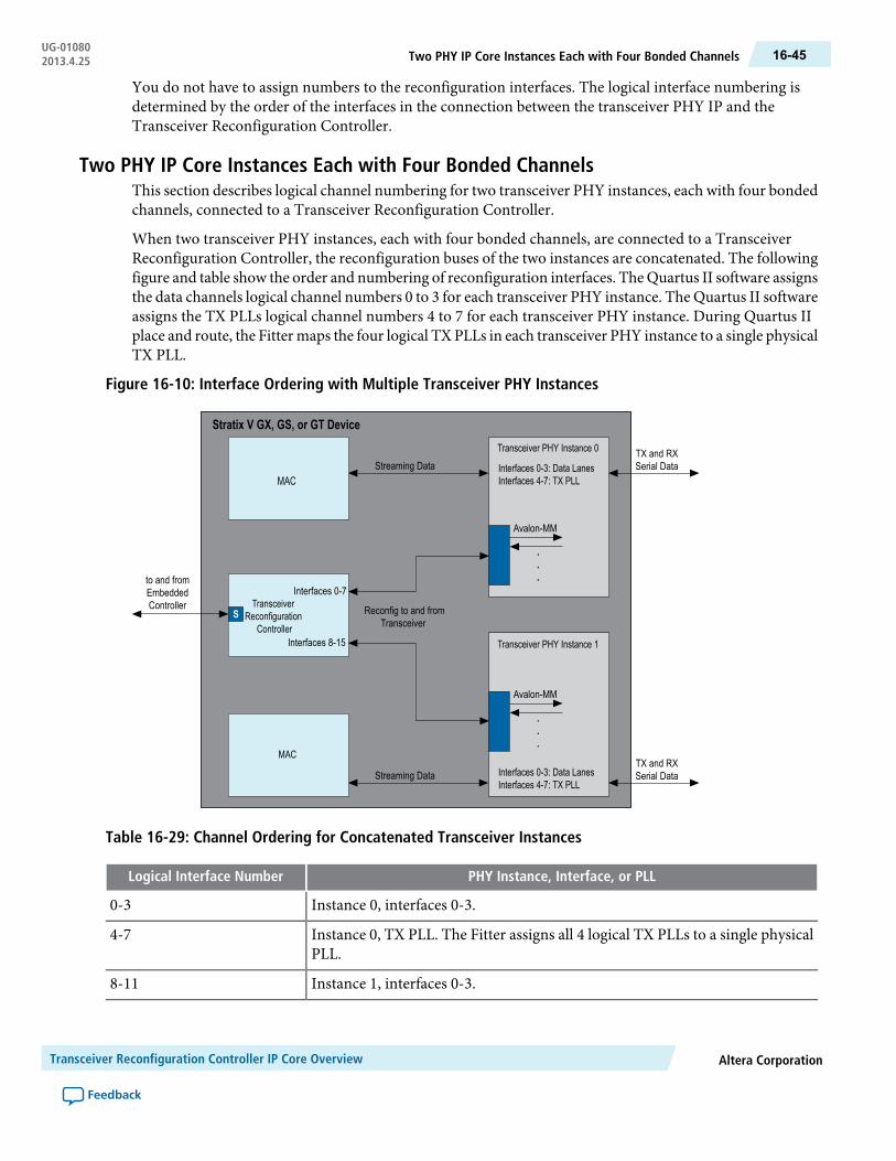
You do not have to assign numbers to the reconfiguration interfaces. The logical interface numbering isdetermined by the order of the interfaces in the connection between the transceiver PHY IP and theTransceiver Reconfiguration Controller.
Two PHY IP Core Instances Each with Four Bonded ChannelsThis section describes logical channel numbering for two transceiver PHY instances, each with four bondedchannels, connected to a Transceiver Reconfiguration Controller.
When two transceiver PHY instances, each with four bonded channels, are connected to a TransceiverReconfiguration Controller, the reconfiguration buses of the two instances are concatenated. The followingfigure and table show the order and numbering of reconfiguration interfaces. TheQuartus II software assignsthe data channels logical channel numbers 0 to 3 for each transceiver PHY instance. The Quartus II softwareassigns the TX PLLs logical channel numbers 4 to 7 for each transceiver PHY instance. During Quartus IIplace and route, the Fitter maps the four logical TX PLLs in each transceiver PHY instance to a single physicalTX PLL.
Figure 16-10: Interface Ordering with Multiple Transceiver PHY Instances
to and fromEmbeddedController Transceiver
ReconfigurationController
S
Interfaces 0-7
Interfaces 8-15
Reconfig to and fromTransceiver
Transceiver PHY Instance 1
Avalon-MM
Streaming Data
Streaming DataTransceiver PHY Instance 0
Avalon-MM
Interfaces 0-3: Data LanesInterfaces 4-7: TX PLL
Interfaces 0-3: Data LanesInterfaces 4-7: TX PLL
TX and RXSerial Data
TX and RXSerial Data
MAC
MAC
Stratix V GX, GS, or GT Device
.
.
.
.
.
.
Table 16-29: Channel Ordering for Concatenated Transceiver Instances
PHY Instance, Interface, or PLLLogical Interface Number
Instance 0, interfaces 0-3.0-3
Instance 0, TX PLL. The Fitter assigns all 4 logical TX PLLs to a single physicalPLL.
4-7
Instance 1, interfaces 0-3.8-11
Altera CorporationTransceiver Reconfiguration Controller IP Core Overview
Feedback
16-45Two PHY IP Core Instances Each with Four Bonded ChannelsUG-010802013.4.25

PHY Instance, Interface, or PLLLogical Interface Number
Instance 1, TX PLL. The Fitter assigns all 4 logical TX PLLs to a single physicalPLL.
12-15
One PHY IP Core Instance with Eight Bonded ChannelsThis section describes logical channel numbering for one transceiver instance with eight bonded channels.
This example requires the Quartus II Fitter to place channels in two, contiguous transceiver banks. Topreserve flexibility for the Fitter, each channel and TX PLL is numbered separately. During place and route,the Fitter maps the eight logical TX PLLs to a single physical TX PLL.
The following table illustrates the logical channel numbering. In this table, logical address 0 accesses datachannel 0 and logical address 8 accesses the TXPLL for data channel 0; logical address 1 accesses data channel1 and logical address 9 accesses the TX PLL for data channel 1, and so on. In simulation, to reconfigure theTX PLL for channel 0, specify logical address 8 in the Streamer module’s logical channel number.The Streamer module maps the logical channel to the physical channel which would be the same value forall eight channels.
Table 16-30: Initial Number of Eight Bonded Channels
Logical Channel NumberChannel
0Channel 0
1Channel 1
2Channel 2
3Channel 3
4Channel 4
5Channel 5
6Channel 6
7Channel 7
8CMU 0
9CMU 1
10CMU 2
11CMU 3
12CMU 4
13CMU 5
14CMU 6
15CMU 7
Transceiver Reconfiguration Controller IP Core OverviewAltera Corporation
Feedback
UG-01080One PHY IP Core Instance with Eight Bonded Channels16-46 2013.4.25
Because all of the channels in a transceiver bank share a PLL, this original numbering allows theFitter to select the optimal CMU PLL from a placement perspective by considering all of the TX PLLsin the bank.
Note:
The following table shows the channel numbers for post-Fitter and hardware simulations. At this point, youshould have assigned channels to pins of the device.
Table 16-31: Post-Fit Logical Channel Numbers for Eight Bonded Channels
Logical Channel NumberChannel
0Channel 0
1Channel 1
2Channel 2
3Channel 3
8-12CMU (0-4)
4Channel 4
5Channel 5
13-15CMU (5-7)
6Channel 6
7Channel 7
Two PHY IP Core Instances Each with Non-Bonded ChannelsThis section describes two instances with non-bonded channels.
For each transceiver PHY IP core instance, the Quartus II software assigns the data channels sequentiallybeginning at logical address 0 and assigns the TX PLLs the subsequent logical addresses.
The following table illustrates the logical channel numbering for two transceiver PHY IP cores, one with 4channels and one with 2 channels.
Altera CorporationTransceiver Reconfiguration Controller IP Core Overview
Feedback
16-47Two PHY IP Core Instances Each with Non-Bonded ChannelsUG-010802013.4.25
Table 16-32: Initial Number of Eight Bonded Channels
Logical Channel NumberChannelInstance
0Channel 0
Instance 0
1Channel 1
2Channel 2
3Channel 3
4CMU 0
5CMU 1
6CMU 2
7CMU 3
8Channel 0
Instance 19Channel 1
10CMU 0
11CMU 1
Transceiver Reconfiguration Controller to PHY IP ConnectivityThis section describes connecting a Transceiver Reconfiguration Controller to the transceiver channels andPLLs in your design.
You can connect a single Transceiver Reconfiguration Controller to all of the transceiver channels and PLLsin your design. You can also use multiple Transceiver Reconfiguration Controllers to facilitate placementand routing of the FPGA. However, the three, upper or lower contiguous channels in a transceiver bankmust be connected to the same reconfiguration controller.
The following figure illustrates connections between the Transceiver Reconfiguration Controller andtransceiver channels after Quartus II compilation.
Transceiver Reconfiguration Controller IP Core OverviewAltera Corporation
Feedback
UG-01080Transceiver Reconfiguration Controller to PHY IP Connectivity16-48 2013.4.25

Figure 16-11: Correct Connections
TransceiverReconfiguration
Controller
Transceiver Bank
3 TransceiverChannels
3 TransceiverChannels
10 GBASE-R
(unused)
(unused)
Custom
Custom
CMU PLL
S
to EmbeddedProcessor
Reconfig toand from
Transceiver
Stratix V GX, GS, or GT Device
The following figure illustrates incorrect connections between two Transceiver Reconfiguration Controllersand six transceiver channels. Two Transceiver Reconfiguration Controllers cannot access a singlereconfiguration interface because there is no arbitration logic to prevent concurrent access. The configurationshown results in a Quartus II compilation error.
Figure 16-12: Incorrect Connections
3 TransceiverChannels
Transceiver Bank
3 TransceiverChannels
Not Allowed
Custom
10 GBASE-R
10 GBASE-R
Custom
Custom
CMU PLL
TransceiverReconfiguration
ControllerS
to EmbeddedProcessor
TransceiverReconfiguration
ControllerS
to EmbeddedProcessor
Reconfig toand from
Transceiver
Stratix V GX, GS, or GT Device
Merging TX PLLs In Multiple Transceiver PHY InstancesThis section describes merging instances of the transceiver PHY.
The Quartus II Fitter can merge the TX PLLs for multiple transceiver PHY IP cores under the followingconditions:
• The PLLs connect to the same reset pin.• The PLLs connect to the same reference clock.• The PLLs connect to the same Transceiver Reconfiguration Controller.
The following figure illustrates a designwhere theCMUPLL in channel 1 provides the clock to threeCustomPHY channels and two 10GBASE-R PHY channels.
Altera CorporationTransceiver Reconfiguration Controller IP Core Overview
Feedback
16-49Merging TX PLLs In Multiple Transceiver PHY InstancesUG-010802013.4.25

Figure 16-13: PLL Shared by Multiple Transceiver PHY IP Cores in a Single Transceiver Bank
Transceiver Bank
to EmbeddedProcessor
Reconfig toand from
Transceiver
Stratix V GX, GS, or GT Device
S M
3 TransceiverChannels
Custom
10 GBASE-R
10 GBASE-RTransceiver
ReconfigurationController
3 TransceiverChannels Custom
Custom
CMU PLL
S
S
Loopback ModesThe PMA analog registers allow you to enable pre- and post-CDR serial loopback modes.
You can enable the pre- and post-CDR reverse serial loopback modes by writing the appropriate bits of theTransceiver Reconfiguration Controller pma_offset register described in PMA Analog Registers. Inpre-CDR mode, data received through the RX input buffer is looped back to the TX output buffer. Inpost-CDR mode, received data passes through the RX CDR and then loops back to the TX output buffer.The RX data is also available to the FPGA fabric. In the TX channel, only the TX buffer is active.
Figure 16-14: Pre- and Post-CDR Reverse Serial Loopback Paths
In this figure, grayed-out blocks are not active in thesemodes. The number (2) shows the post-CDR loopbackpath and the number (3) shows pre-CDR reverse serial loopback path.
Tx PCS
Rx PCS
Tx PMA
Serializer
Rx PMA
Deserializer
To FPGA fabricfor verification
Transceiver
CDR
(2) (3)FPGAFabric
In addition to the pre-CDR and post-CDR loopback modes available in the Transceiver ReconfigurationController register map, all the of PHYs, with the exception of PCI Express, support serial loopback mode.You enable this mode by writing the phy_serial_loopback register (0x061) using the Avalon-MM
Transceiver Reconfiguration Controller IP Core OverviewAltera Corporation
Feedback
UG-01080Loopback Modes16-50 2013.4.25
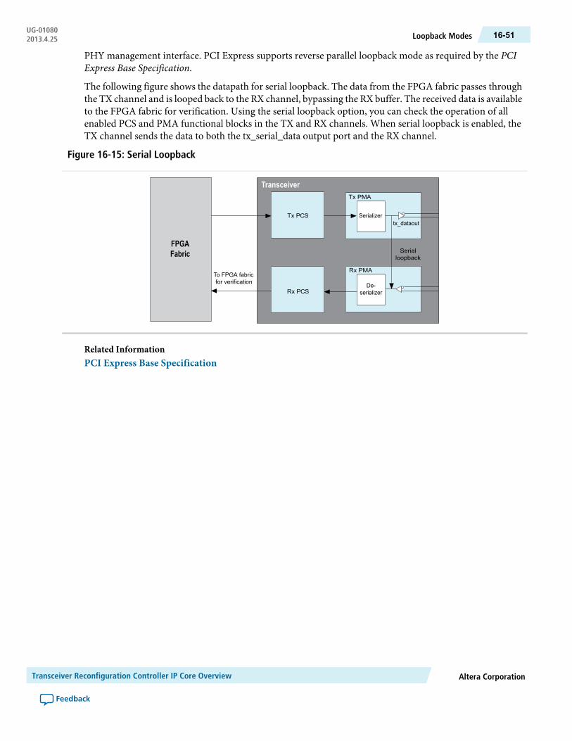
PHY management interface. PCI Express supports reverse parallel loopback mode as required by the PCIExpress Base Specification.
The following figure shows the datapath for serial loopback. The data from the FPGA fabric passes throughthe TX channel and is looped back to the RX channel, bypassing the RX buffer. The received data is availableto the FPGA fabric for verification. Using the serial loopback option, you can check the operation of allenabled PCS and PMA functional blocks in the TX and RX channels. When serial loopback is enabled, theTX channel sends the data to both the tx_serial_data output port and the RX channel.
Figure 16-15: Serial Loopback
Tx PCS
Rx PCS
FPGAFabric
Tx PMA
tx_dataoutSerializer
Rx PMA
Serialloopback
De-serializer
To FPGA fabricfor verification
Transceiver
Related InformationPCI Express Base Specification
Altera CorporationTransceiver Reconfiguration Controller IP Core Overview
Feedback
16-51Loopback ModesUG-010802013.4.25

17Transceiver PHY Reset Controller IP Core
2013.4.25UG-01080 Subscribe Feedback
The Transceiver PHY Reset Controller IP Core is a highly configurable core that you can use to resettransceivers in Arria V, Arria V GZ, Cyclone V, or Stratix V devices. This reset controller is an alternatecontroller that you can use instead of the embedded reset controller for the Custom, Low Latency, andDeterministic Latency PHY IP cores. And, you can use it to reset the Stratix V, Arria V, Arria V GZ, andCyclone V Native Transceiver PHYs which do not include imbedded reset controllers. You can use it tospecify a custom reset sequence. You can also modify the clear text Verilog HDL file provided to implementcustom reset logic. The Reset Controller handles all reset sequencing of the transceiver to enable successfuloperation. It provides the functionality of the embedded reset controller and the following additional options:
• Separate or shared reset controls per channel• Separate controls for the TX and RX channels and PLLs• Synchronization of the reset inputs• Hysteresis for PLL locked status inputs• Configurable reset timings• Automatic or manual reset recovery mode
ISO9001:2008Registered
© 2013 Altera Corporation. All rights reserved. ALTERA, ARRIA, CYCLONE, HARDCOPY, MAX, MEGACORE, NIOS, QUARTUS and STRATIXwords and logos are trademarks of Altera Corporation and registered in the U.S. Patent and Trademark Office and in other countries. All other wordsand logos identified as trademarks or service marks are the property of their respective holders as described at www.altera.com/common/legal.html.Altera warrants performance of its semiconductor products to current specifications in accordance with Altera's standard warranty, but reserves theright to make changes to any products and services at any time without notice. Altera assumes no responsibility or liability arising out of the applicationor use of any information, product, or service described herein except as expressly agreed to in writing by Altera. Altera customers are advised toobtain the latest version of device specifications before relying on any published information and before placing orders for products or services.
www.altera.com
101 Innovation Drive, San Jose, CA 95134
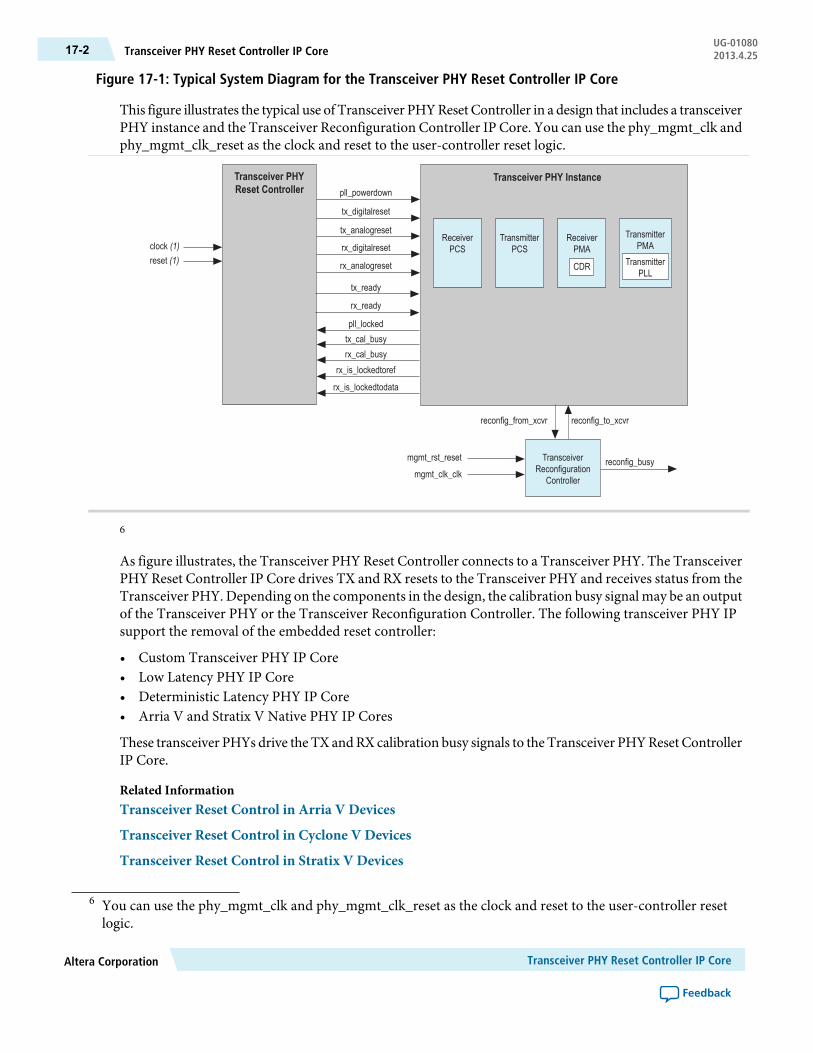
Figure 17-1: Typical System Diagram for the Transceiver PHY Reset Controller IP Core
This figure illustrates the typical use of Transceiver PHYReset Controller in a design that includes a transceiverPHY instance and the Transceiver Reconfiguration Controller IP Core. You can use the phy_mgmt_clk andphy_mgmt_clk_reset as the clock and reset to the user-controller reset logic.
clock (1)reset (1)
tx_cal_busyrx_cal_busy
Transceiver PHY InstanceTransceiver PHYReset Controller
rx_is_lockedtoref
pll_locked
rx_is_lockedtodata
reconfig_busymgmt_rst_reset
mgmt_clk_clk
reconfig_from_xcvr reconfig_to_xcvr
TransceiverReconfiguration
Controller
rx_digitalreset
pll_powerdown
rx_analogreset
tx_ready
rx_ready
tx_digitalreset
ReceiverPMA
CDR
TransmitterPCS
TransmitterPMA
ReceiverPCS
tx_analogreset
TransmitterPLL
6
As figure illustrates, the Transceiver PHY Reset Controller connects to a Transceiver PHY. The TransceiverPHY Reset Controller IP Core drives TX and RX resets to the Transceiver PHY and receives status from theTransceiver PHY. Depending on the components in the design, the calibration busy signal may be an outputof the Transceiver PHY or the Transceiver Reconfiguration Controller. The following transceiver PHY IPsupport the removal of the embedded reset controller:
• Custom Transceiver PHY IP Core• Low Latency PHY IP Core• Deterministic Latency PHY IP Core• Arria V and Stratix V Native PHY IP Cores
These transceiver PHYs drive the TX andRX calibration busy signals to the Transceiver PHYReset ControllerIP Core.
Related InformationTransceiver Reset Control in Arria V Devices
Transceiver Reset Control in Cyclone V Devices
Transceiver Reset Control in Stratix V Devices
6 You can use the phy_mgmt_clk and phy_mgmt_clk_reset as the clock and reset to the user-controller resetlogic.
Transceiver PHY Reset Controller IP CoreAltera Corporation
Feedback
UG-01080Transceiver PHY Reset Controller IP Core17-2 2013.4.25
Device Family Support for Transceiver PHY Reset ControllerThis section describes the transceiver PHY reset controller IP core device family support.
IP cores provide either final or preliminary support for target Altera device families. These terms have thefollowing definitions:
• Final support—Verified with final timing models for this device.• Preliminary support—Verified with preliminary timing models for this device.
Table 17-1: Device Family Support
This table lists the level of support offered by the Transceiver PHY Reset Controller IP core for Altera devicefamilies.
SupportDevice Family
PreliminaryCyclone V devices
PreliminaryArria V devices
PreliminaryArria V GZ
PreliminaryStratix V devices
No supportOther device families
Performance and Resource Utilization for Transceiver PHY Reset ControllerThis section describes the performance and resource utilization for the transceiver PHY reset controller.
Table 17-2: Reset Controller Resource Utilization—Stratix V Devices
This table lists the typical expected device resource utilization, rounded to the nearest 50, for two configurationsusing the current version of the Quartus II software targeting a Stratix V GX device. The numbers are roundedto the nearest 50.
Logic RegistersCombinational ALUTsConfiguration
5050Single channel
1501004 channels, sharedTX reset, separateRX resets
Parameterizing the Transceiver PHY Reset Controller PHYThis section provides a list of steps required to configure the Transceiver PHY Reset Controller IP Core inthe MegaWizard Plug-In Manager.
Complete the following steps to configure the Transceiver PHYReset Controller IPCore in theMegaWizardPlug-In Manager:
1. For Which device family will you be using?, select Arria V, Arria V GZ, Cyclone V, or Stratix V fromthe list.
2. Click Installed Plug-Ins > Interfaces > Transceiver PHY > Transceiver PHY Reset Controller v12.1.
Altera CorporationTransceiver PHY Reset Controller IP Core
Feedback
17-3Device Family Support for Transceiver PHY Reset ControllerUG-010802013.4.25

3. Select the options required for your design. For a description of these options, refer to the TransceiverPHY Reset Controller Parameters.
4. Click Finish.Generates your customized Transceiver PHY Reset Controller IP Core.
Transceiver PHY Reset Controller Parameters
Table 17-3: General Options
This table lists the parameters that you can set to customize the Transceiver PHY Reset Controller IP Core.DescriptionRangeName
Specifies the number of channels thatconnect to the Transceiver PHY ResetController IP Core.
1-1000Number of transceiver channels
Specifies the number of TX PLLs thatconnect to the Transceiver PHY ResetController.
1-1000Number of TX PLLS
Input clock to the transceiver PHY ResetController. The frequency of the input clockin MHz. The upper limit on the input clockfrequency is the frequency achieved intiming closure.
1-500 MHzInput clock frequency
When On , the Transceiver PHY ResetController synchronizes the reset to theTransceiver PHY Reset Controller inputclock before driving it to the internal resetlogic. When Off, the reset input is notsynchronized.
On /OffSynchronize reset input
When On, the Transceiver PHY ResetController uses reduced reset counters forsimulation.WhenOff, simulation runs withthe actual timings for hardware.
On /OffUse fast reset for simulation
TX PLL
When On, the Transceiver PHY ResetController enables the control of the TXPLL.WhenOff, the TXPLL controls are disabled.
On /OffEnable TX PLL channel resetcontrol
Specifies the duration of the PLLpowerdownperiod in ns. The value is rounded up to thenearest clock cycle. The default value is 1000ns.
1-999999999pll_powerdown duration
Transceiver PHY Reset Controller IP CoreAltera Corporation
Feedback
UG-01080Transceiver PHY Reset Controller Parameters17-4 2013.4.25
DescriptionRangeName
When On, the Transceiver PHY ResetController synchronizes thePLLpowerdownreset with the Transceiver PHY ResetController input clock. When Off, the PLLpowerdown reset is not synchronized. If youselect this option, you must also enable theSynchronize reset input parameter. Turningthis option On prevents equivalent PLLsfrom being merged across Transceiver PHYReset Controllers.
On /OffSynchronize reset input for PLLpowerdown
TX Channel
When On, the Transceiver PHY ResetController enables the control logic andassociated status signals for TX reset. WhenOff, disables TX reset control and statussignals.
On /OffEnable TX channel reset control
When On, each TX channel has a separatereset.WhenOff, the Transceiver PHYResetController uses a shared TX reset controllerfor all channels.
On /OffUse separate TX reset per channel
Specifies the Transceiver PHY ResetController behaviorwhen thepll_lockedsignal is deasserted. The following modesare available:
• Auto : The associated tx_digital_reset controller automatically resetswhenever the pll_locked signal isdeasserted.
• Manual :The associatedtx_digital_reset controller is not reset when thepll_locked signal is deasserted,allowing you to choose corrective action.
• Expose Port :Thetx_manual signal isa top-level signal of the IP Core.
Auto,ManualExpose,PortTXautomatic reset recoverymode
Specifies the time in ns to continue to assertthe tx_digitalreset after the resetinput and all other gating conditions areremoved. The value is rounded up to thenearest clock cycle. The default value is 20ns.
1-999999999tx_digitalreset duration
Specifies the amount of hysteresis in ns toadd to the pll_locked status input tofilter spurious unreliable assertions of thepll_locked signal. A value of 0 adds nohysteresis. A higher values filters glitches onthe pll_locked signal.
1-999999999pll_locked input hysteresis
Altera CorporationTransceiver PHY Reset Controller IP Core
Feedback
17-5Transceiver PHY Reset Controller ParametersUG-010802013.4.25

DescriptionRangeName
RX Channel
When On, the Transceiver PHY ResetController enables the control logic andassociated status signals for RX reset. WhenOff, disables RX reset control and statussignals.
On /OffEnable RX channel reset control
When On, each RX channel has a separatereset input.WhenOff, uses a sharedRX resetcontroller for all channels.
On /OffUse separate RX reset per channel
Specifies the Transceiver PHY ResetController behaviorwhen thepll_lockedsignal is deasserted. The following modesare available:
• Auto : The associated rx_digital_reset controller automatically resetswhenever therx_is_lockedtodatasignal is deasserted.
• Manual :The associatedrx_digital_reset controller is not reset when therx_is_lockedtodata signal isdeasserted, allowing you to choosecorrective action.
• Expose Port :Therx_manual signal isa top-level signal of the IP Core. If thecore includes separate reset control foreach RX channel, each RX channel usesits respectiverx_is_lockedtodatasignal for automatic reset control;otherwise, the inputs are AND ed toprovide internal status for the sharedreset controller.
Auto,ManualExpose,PortRXautomatic reset recoverymode
Specifies the time in ns to continue to asserttherx_analogreset after the reset inputand all other gating conditions are removed.The value is rounded up to the nearest clockcycle. The default value is 4000 ns.
1-999999999rx_analogreset duration
Specifies the time in ns to continue to assertthe rx_digitalreset after the resetinput and all other gating conditions areremoved. The value is rounded up to thenearest clock cycle. The default value is 40ns.
1-999999999rx_digitalreset duration
Transceiver PHY Reset Controller IP CoreAltera Corporation
Feedback
UG-01080Transceiver PHY Reset Controller Parameters17-6 2013.4.25

Interfaces for Transceiver PHY Reset ControllerThis section describes the top-level signals for the transceiver PHY reset controller IP core.
The following figure illustrates the top-level signals of the Transceiver PHY Reset Controller IP Core. Manyof the signals in figure become buses if you choose separate reset controls. The variables in figure representthe following parameters:
• <n>—The number of lanes• <p>—The number of PLLs
Figure 17-2: Top-Level Signals of the Transceiver PHY Reset Controller
pll_locked[<p>-1:0]pll_select[<p>-1:0]tx_cal_busy[<n>-1:0]rx_cal_busy[<n>-1:0]rx_is_lockedtodata[<n>-1:0]
tx_manual[<n>-1:0]rx_manual[<n>-1:0]
clockreset
Transceiver PHY Reset Controller Top-Level Signals
tx_digitalreset[<n>-1:0]tx_analogreset[<n>-1:0]
tx_ready[<n>-1:0]
rx_digitalreset[<n>-1:0]rx_analogreset[<n>-1:0]
rx_ready[<n>-1:0]
pll_powerdown[<p>-1:0]
PLL andCalibration
Status
PLL Powerdown
TX and RXResets and Status
Clockand Reset
PLLControl
Table 17-4: Top-Level Signals
This table describes the signals in the above figure in the order that they are shown in the figure.DescriptionDirectionSignal Name
Input Signals
Provides the PLL locked status input for each PLL.When asserted, indicates that the TXPLL is locked.When deasserted, the PLL is not locked. There isone signal per PLL. When an IP core uses multiplePLLs, the pll_select signals specifies the PLLto use.
Inputpll_locked[ <p> -1:0]
Whenyou selectUse separate TX reset per channel,this bus provides enough inputs to specify an indexfor each pll_locked signal to listen to for eachchannel. When you select a shared TX reset, thepll_select signal specifies the pll_lockedsignal used for all channels. This signal issynchronous to the Transceiver PHY ResetController input clock.
Inputpll_select
This is the calibration status signal from theTransceiver PHY IP Core. When asserted,calibration is active. When deasserted, calibrationhas completed. This signal gates the TX resetsequence. Thewidth of this signals depends on thenumber of TX channels.
Inputtx_cal_busy[ <n> -1:0]
Altera CorporationTransceiver PHY Reset Controller IP Core
Feedback
17-7Interfaces for Transceiver PHY Reset ControllerUG-010802013.4.25
DescriptionDirectionSignal Name
This is calibration status signal from theTransceiver PHY IP Core. When asserted,calibration is active. When deasserted, calibrationhas completed. This signal gates the RX resetsequence. Thewidth of this signals depends on thenumber of RX channels.
Inputrx_cal_busy[ <n> -1:0]
Provides the rx_is_lockedtodata statusfrom each RX CDR. When asserted, indicates thata particular RXCDR is ready to receive input data.If you do not choose separate controls for the RXchannels, these inputs are AND ed togetherinternally to provide a single status signal.
Inputrx_is_lockedtodata[ <n>-1:0]
This optional signal places tx_digitalresetcontroller under automatic or manual control.When asserted, the associated tx_digitalreset controller does notautomatically respond to deassertion of the pll_locked signal. However, the initial tx_digitalreset sequence still requires aone-time rising edge on pll_locked beforeproceeding. When deasserted, the associated tx_digital_reset controller automatically beginsits reset sequence whenever the selected pll_locked signal is deasserted.
Inputtx_manual[ <n> -1:0]
This optional signal places rx_digitalresetcontroller under automatic or manual control. Inmanualmode, therx_digitalreset controllerdoes not respond to the assertion or deassertionof the rx_is_lockedtodata signal. Therx_digitalreset controller asserts rx_readywhen thepll_locked signal is asserted.
Inputrx_manual[ <n> -1:0]
System clock input to the Transceiver PHY ResetController from which all internal logic is driven.
Inputclock
Asynchronous reset input to the Transceiver PHYReset Controller. When asserted, all configuredreset outputs are asserted. Holding the reset inputsignal asserted holds all other reset outputsasserted.
Inputreset
Output Signals
Transceiver PHY Reset Controller IP CoreAltera Corporation
Feedback
UG-01080Interfaces for Transceiver PHY Reset Controller17-8 2013.4.25

DescriptionDirectionSignal Name
Digital reset for TX. The width of this signaldepends on the number of TX channels. This signalis asserted when any of the following conditionsis true:
• reset is asserted• pll_powerdown is asserted• tx_cal_busy is asserted• PLL has not reached the initial lock (pll_
locked deasserted)• pll_locked is deasserted andtx_manual
is deasserted
When all of these conditions are false, the resetcounter begins its countdown for deassertion oftx_digital_reset.
Outputtx_digitalreset[ <n> -1:0]
Analog reset for TX channels. This signal followspll_powerdown and is deasserted a few clockcycles after the TX PLL comes out the reset andlocks to the input reference clock.
Outputtx_analogreset[ <n> -1:0]
Status signal to indicate when the TX resetsequence is complete. This signal is deassertedwhile the TX reset is active. It is asserted a fewclock cycles after the deassertion of tx_digitalreset. Thewidthof this signal dependson the number of TX channels.
Outputtx_ready[ <n> -1:0]
Digital reset for RX. The width of this signaldepends on the number of channels. This signal isasserted when any of the following conditions istrue:
• reset is asserted• rx_analogreset is asserted• rx_cal_busy is asserted• rx_is_lockedtodata is deasserted and
rx_manual is deasserted
When all of these conditions are false, the resetcounter begins its countdown for deassertion ofrx_digital_reset.
Outputrx_digitalreset[ <n> -1:0]
Status signal to indicate when the RX resetsequence is complete. This signal is deassertedwhile the RX reset is active. It is asserted a fewclock cycles after the deassertion of rx_digitalreset. Thewidthof this signal dependson the number of channels.
Outputrx_ready[ <n> -1:0]
Altera CorporationTransceiver PHY Reset Controller IP Core
Feedback
17-9Interfaces for Transceiver PHY Reset ControllerUG-010802013.4.25

DescriptionDirectionSignal Name
Asserted to power down a transceiver PLL circuit.When asserted, the selected TX PLL is reset. Bydefault, the Native Transceiver PHY IP Corescreate a separatepll_powerdown signal for eachlogical PLL. PLLs can only bemerged if theirpll_powerdown signals are driven from the samesource. However, the Fitter may merge the PLLsif they are in the same transceiver bank. If the PLLsare in separate transceiver banks, you can chooseto drive thepll_powerdown signals separately.
Outputpll_powerdown[ <p> -1:0]
Timing Constraints for Reset Signals when Using Bonded PCS ChannelsFor designs that use bonded TXPCS channels, the reset signal to all TX PCS channels within a bonded groupmust meet a maximum skew tolerance. This skew tolerance is one-half the TX parallel clock cycle.
You must provide a Synopsys Design Constraint (SDC) for the reset signals to guarantee that your designmeets timing. The following example shows the general form for this constraint. If your design includes theTransceiver PHYReset Controller IP Core or the embedded reset controller, you can substitute your instanceand interface names for the generic names shown in example.
Example 17-1: SDC Constraint for TX Digital Reset When Bonded Clocks Are Used
set_max_skew -from *<IP_INSTANCE_NAME>*tx_digitalreset*r_reset-to *pld_pcs_interface* <1/2 coreclk period in ps>
In the above example, you must make the following substitutions:
• <IP_INSTANCE_NAME>—substitute the name of your reset controller IP instance or PHY IP instance• <1/2 coreclk period in ps>—substitute the 1/2 the clock period of your design in picoseconds
If your design has custom reset logic, replace the*<IP_INSTANCE_NAME>*tx_digital_reset*r_reset with the source register for the TX PCSreset signal, tx_digital_reset.
Altera believes thatmost designswillmeet thismaximum skew requirementwithout this constraint; however,it cannot be guaranteed without including this constraint.
Formore information about theset_max_skew constraint, refer to the SDCandTimeQuestAPIReferenceManual.
Related InformationSDC and TimeQuest API Reference Manual
Transceiver PHY Reset Controller IP CoreAltera Corporation
Feedback
UG-01080Timing Constraints for Reset Signals when Using Bonded PCS Channels17-10 2013.4.25

18Transceiver PLL IP Core for Stratix V, ArriaV, and Arria V GZ Devices
2013.4.25UG-01080 Subscribe Feedback
When a fractional PLL functions as the TX PLL, you must configure the Native PHY IP Core to use externalPLLs. If you also want to use CMU or ATX PLLs, you must use the device-specific Transceiver PLL toinstantiate them.
The MegaCore Library includes the following IP cores to instantiate external CMU and ATX PLLs:
• Stratix V Transceiver PLL• Arria V Transceiver PLL• Arria V GZ Transceiver PLL
You instantiate the Altera Phase-Locked Loop (ALTERA_ PLL) IP Core to specify the fractional PLL andtheNative PHY IPCore to specify the PMAand PCS settings. In theNative PHYGUI, select theUse externalTXPLL option under theTXPLLOptions heading. When you choose this option, the Native PHY includesa top-level bus,ext_pll_clk[<p>-1:0] that you can connect to the external CMU,ATX, and fractionalPLLs. To achieve different TX channel data rates, you create point-to-point connections betweenext_pll_clk[<p>-1:0] and the CMU, ATX, and fractional PLLs required.
Figure 18-1: IP Cores Required for Designs Using the Fractional PLL
The following figure show the IP Cores you can instantiate to create designs that use a fractional PLL as theTX PLL. The figure also illustrates the use of Transceiver PLL to instantiate CMU and ATX PLLs. TheMegaCore Library includes separate Transceiver PLL and Native PHY IP Cores for each V-Series DeviceFamily. This figure shows logical connectivity between IP Cores and does not reflect the physical locationof hardware in V-Series devices.
Altera Phased-Locked Loop(ALTERA_PLL)
Fractional PLL
Native PHYTransceiver PLL
CMU PLL
Transceiver PLL
ATX PLL
SerializerLocal ClockDivider(LCD)
Channel 1
(Stratix V and Arria V GZ, only)
SerializerLocal ClockDivider(LCD)
Channel 0
ISO9001:2008Registered
© 2013 Altera Corporation. All rights reserved. ALTERA, ARRIA, CYCLONE, HARDCOPY, MAX, MEGACORE, NIOS, QUARTUS and STRATIXwords and logos are trademarks of Altera Corporation and registered in the U.S. Patent and Trademark Office and in other countries. All other wordsand logos identified as trademarks or service marks are the property of their respective holders as described at www.altera.com/common/legal.html.Altera warrants performance of its semiconductor products to current specifications in accordance with Altera's standard warranty, but reserves theright to make changes to any products and services at any time without notice. Altera assumes no responsibility or liability arising out of the applicationor use of any information, product, or service described herein except as expressly agreed to in writing by Altera. Altera customers are advised toobtain the latest version of device specifications before relying on any published information and before placing orders for products or services.
www.altera.com
101 Innovation Drive, San Jose, CA 95134
Designs that dynamically reconfigure the TXPLL between theCMUPLL and fractional PLL,must also selectUse external TX PLL in the Native PHY GUI and instantiate all PLLs externally as shown in the figureabove. Dynamic reconfiguration is only supported for non-bonded configurations. Dynamic reconfigurationallows you to implement the following features:
• TX PLL reconfiguration between up to 5 input reference clocks• PLL switching using the x1 clock lines within a transceiver triplet• PLL switching using the x6 and xN clock lines when the TX channels are not in the same transceiver
bank
Related InformationAltera Phase-Locked Loop (ALTERA_PLL) Megafunction User Guide
Arria V Transceiver Native PHY IP Core on page 13-1
Arria V GZ Transceiver Native PHY IP Core on page 14-1
Stratix V Transceiver Native PHY IP Core on page 12-1
Parameterizing the Transceiver PLL PHYThe MegaWizard Plug-In Manger Library provides the following Transceiver PLL IP Cores: Arria VTransceiver, Arria V GZ Transceiver PLL, and Stratix V Transceiver PLL to be used with the Arria V, ArriaV GZ and Stratix V Native PHYs, respectively.
Complete the following steps to configure a Transceiver PLL IP Core in the MegaWizard Plug-In Manager:
1. For Which device family will you be using?, select Arria V, Arria V GZ, or Stratix V from the list.2. Click Installed Plug-Ins > Interfaces > Transceiver PHY> <Device> Transceiver PLL <ver>.3. Specify the options required for the PLL.4. Click Finish to generate your parameterize Transceiver PLL IP Core.
Transceiver PLL Parameters
Table 18-1: PLL Reconfigurations
DescriptionValueName
You must enable this option if you plan to reconfigurethe PLLs in your design. This option is also requiredto simulate PLL reconfiguration.
On/OffEnable PLLReconfiguration
Specifies the number of reference clocks inputs to theTransceiver PLL.
1-5Number of TX referenceclocks
Select theExternal feedback path for theCPRI protocolto improve clock jitter by using an external voltagecontrolled crystal oscillator (VCXO). Select Internalfor all other protocols.
Internal
External
PLL feedback path
Transceiver PLL IP Core for Stratix V, Arria V, and Arria V GZ DevicesAltera Corporation
Feedback
UG-01080Parameterizing the Transceiver PLL PHY18-2 2013.4.25

DescriptionValueName
Specifies the PLL type. You must select the CMU PLLfor designs that also include a fractional PLL. TheATXpll is available for Stratix V and Arria V GZ devices.
CMU
ATX
PLL Type
Specifies Base data rate. This value should match thevalue specified in the Native PHY.
1 × Lane rate
2 × Lane rate
4 × Lane rate
8 × Lane rate
PLL base data rate
Specifies the frequency of the PLL input reference clock.The PLLmust generate an output frequency that equalsthe Base data rate/2. You can use any Input clockfrequency that allows the PLLs to generate this outputfrequency.
VariableReference clock frequency
Specifies the index of the TX reference clock for theinitial configuration of the TX PLL. Logical index 0corresponds to TX reference clock 1, and so on.
0-4Selected reference clocksource
Transceiver PLL SignalsFigure 18-2: Transceiver PLL Top-Level Signals
The following figure illustrates the top-level signals of the Transceiver PLL which are defined in the tablebelow.
pll_powerdownpll_refclk[<p>-1:0]pll_fbclk
pll_clkoutpll_locked
reconfig_to_xcvr[69:0]reconfig_from_xcvr[45:0]
Transceiver PL L Top-Level Signals
PL L Clockand StatusPL L
Inputs DynamicReconfiguration
(optional)
DescriptionDirectionSignal Name
When asserted, powers down the PLL.Inputpll_powerdown
Input reference clock for the CMU PLL.Inputpll_refclk
The feedback input port for the PLL.Inputpll_fbclk
Output clock from the PLL.Outputpll_clkout
When asserted, indicates that the PLL has locked to the inputreference clock.
Outputpll_locked
Altera CorporationTransceiver PLL IP Core for Stratix V, Arria V, and Arria V GZ Devices
Feedback
18-3Transceiver PLL SignalsUG-010802013.4.25
DescriptionDirectionSignal Name
Reconfiguration signals from the Transceiver ReconfigurationController. When you enable the reconfiguration bus, thesimulation model for the TX PLL supports dynamicreconfiguration. When you enable this bus, the Quartus IIsoftware does not merge TX PLL by default; however, you canmerge TX PLLs using QSF settings.
Inputreconfig_to_xcvr[69:0]
Reconfiguration signals to the Transceiver ReconfigurationController.
Outputreconfig_from_xcvr[45:0]
Related InformationComponent Interface Tcl Reference
Transceiver PLL IP Core for Stratix V, Arria V, and Arria V GZ DevicesAltera Corporation
Feedback
UG-01080Transceiver PLL Signals18-4 2013.4.25

19Analog Parameters Set Using QSFAssignments
2013.4.25UG-01080 Subscribe Feedback
You specify the analog parameters using the Quartus II Assignment Editor, the Pin Planner, or through theQuartus II Settings File (.qsf). The default values for analog options fall into three categories:
• Global— These parameters have default values that are independent of other parameter settings.• Computed—These parameters have an initial default value that is recomputed based on other parameter
settings.• Proxy—These parameters have default values that are place holders. The Quartus II software selects these
initial default values based on your design; however, Altera recommends that you replace these defaultswith values that match your electrical board specification.
For more information about the Pin Planner, refer to About the Pin Planner in Quartus II Help. For moreinformation about the Assignment Editor, refer to About the Assignment Editor in Quartus II Help.
For more information about Quartus II Settings, refer to Quartus II Settings File Manual.
Related InformationAbout the Pin Planner
About the Assignment Editor
Quartus II Settings File Manual
Making QSF Assignments Using the Assignment EditorThe Quartus II software provides default values for analog parameters. You can change the default valuesusing the Assignment Editor. For example, complete the following steps to specify a 3.0V supply for theVCCA voltage and a 1.0V supply to the VCCR voltages.
1. On the Assignments menu, select Assignment Editor. The Assignment Editor appears.2. Complete the following steps for each pin requiring the VCCA voltage:
a. Double-click in the Assignment Name column and scroll to the bottom of the available assignments.b. Select VCCA_GXB Voltage.c. In the Value column, select 3_0V from the list.
3. Complete the following steps for each pin requiring the VCCR voltage:a. Double-click in the Assignment Name column and scroll to the bottom of the available assignments.b. Select VCCR_GXB/VCCT_GXB Voltage.c. In the Value column, select 1_0V from the list.
ISO9001:2008Registered
© 2013 Altera Corporation. All rights reserved. ALTERA, ARRIA, CYCLONE, HARDCOPY, MAX, MEGACORE, NIOS, QUARTUS and STRATIXwords and logos are trademarks of Altera Corporation and registered in the U.S. Patent and Trademark Office and in other countries. All other wordsand logos identified as trademarks or service marks are the property of their respective holders as described at www.altera.com/common/legal.html.Altera warrants performance of its semiconductor products to current specifications in accordance with Altera's standard warranty, but reserves theright to make changes to any products and services at any time without notice. Altera assumes no responsibility or liability arising out of the applicationor use of any information, product, or service described herein except as expressly agreed to in writing by Altera. Altera customers are advised toobtain the latest version of device specifications before relying on any published information and before placing orders for products or services.
www.altera.com
101 Innovation Drive, San Jose, CA 95134

The Quartus II software adds these instance assignments commands to the .qsf file for your project.
Analog Settings for Arria V DevicesThis section lists the analog parameters for Arria V devices whose original values are place holders for thevalues that match your electrical board specification. In the following table, the default value of an analogparameter is shown in bold type. The parameters are listed in alphabetical order.
Table 19-1: Transceiver and PLL Assignments for Arria V Devices
Assign ToOptionsDescriptionPin Planner andAssignment Editor
Name
QSF Assignment Name
Pin - TX& RXserialdata
85_Ohms
100_Ohms
120_Ohms
150_Ohms
External_Resistor
Specifies the intended on-chiptermination value for the specifiedtransceiver pin. Use ExternalResistor if you intend to useoff-chip termination.
Transceiver I/OPin Termination
XCVR_IO_PIN_TERMINATION
Analog Parameters Set Using QSF AssignmentsAltera Corporation
Feedback
UG-01080Analog Settings for Arria V Devices19-2 2013.4.25
Assign ToOptionsDescriptionPin Planner andAssignment Editor
Name
QSF Assignment Name
Pin - PLLrefclk pin
AC_coupling
DC_coupling_internal_100_OhmS
DC_coupling_external_ resistor
Specifies the intended terminationvalue for the specified refclk pin.The following 3 settings areavailable:
• AC_COUPLING: Alterarecommends this setting for alltransceiver designs. Use it forAC coupled signals. Thissetting implements on-chiptermination and on-chip signalbiasing.
• DC_COUPLING_INTERNAL_100_OHM: Usedthis setting when the dedicatedtransceiver reference clock pinsare fed by a DC coupled signalwhose Vcm meets the devicespecification. This assignmentimplements internal on-chiptermination but not on-chipsignal biasing.
• DC_COUPLING_EXTERNAL_RESISTOR:Usethis assignment when thededicated transceiver referenceclock pins are fed by a DCcoupled signal. This optiondoes not implement internalon-chip termination or signalbiasing. You must implementtermination and signal biasingoutside of the FPGA. Thisassignment is recommendedfor compliance with the PCIExpress Card ElectromechanicalSpecification Rev. 2.0 and theHCSL IO Standard.
TransceiverDedicated RefclkPin Termination
XCVR_REFCLK_ PIN_TERMINATION
Altera CorporationAnalog Parameters Set Using QSF Assignments
Feedback
19-3Analog Settings for Arria V DevicesUG-010802013.4.25
Assign ToOptionsDescriptionPin Planner andAssignment Editor
Name
QSF Assignment Name
Pin - TXserialdata
1–5Specifies the slew rate of the outputsignal. The following encodingsare defined:
• 1: SLEW_160PS• 2: SLEW_90PS• 3: SLEW_50PS• 4: SLEW_30PS• 5: SLEW_15PS
Transmitter SlewRate Control
XCVR_TX_SLEW_RATE_CTRL
Pin - TX& RXserialdata
ArriaVGX: 1_1V
ArriaVGT: 1_2V
Configures the VCCR_GXB andVCCT_GXB voltage for an GXBI/O pin by specifying the intendedsupply voltages for a GXB I/O pin.This voltage is fixed at 1_1V for allfrequency ranges.
VCCR_GXB
VCCT_GXBVoltage
XCVR_VCCR_ VCCT_VOLTAGE
The following table lists the analog parameters with global or computed default values. You may want tooptimize some of these settings. The default value is shown in bold type. For computed analog parameters,the default value listed is for the initial setting, not the recomputed setting. The parameters are listed inalphabetical order.
Table 19-2: Transceiver and PLL Assignments for Arria V Devices
Assign ToOptionsDescriptionPin Planner and Assign-ment Editor Name
QSF Assignment Name
Analog Parameters with Global Default Value
PLLinstance
Auto
Low
Medium
High
Specifies the CDRbandwidth presetsetting
CDR BandwidthPreset
CDR_BANDWIDTH_PRESET
PLLinstance
Auto
Low
Medium
High
Specifies the PLLbandwidth presetsetting
PLLBandwidthPresetPLL_BANDWIDTH_PRESET
Pin - RXserial data
0 –1Controls the amountof a stagereceive-bufferDCgain.
Receiver Buffer DCGain Control
XCVR_RX_DC_GAIN
Analog Parameters Set Using QSF AssignmentsAltera Corporation
Feedback
UG-01080Analog Settings for Arria V Devices19-4 2013.4.25
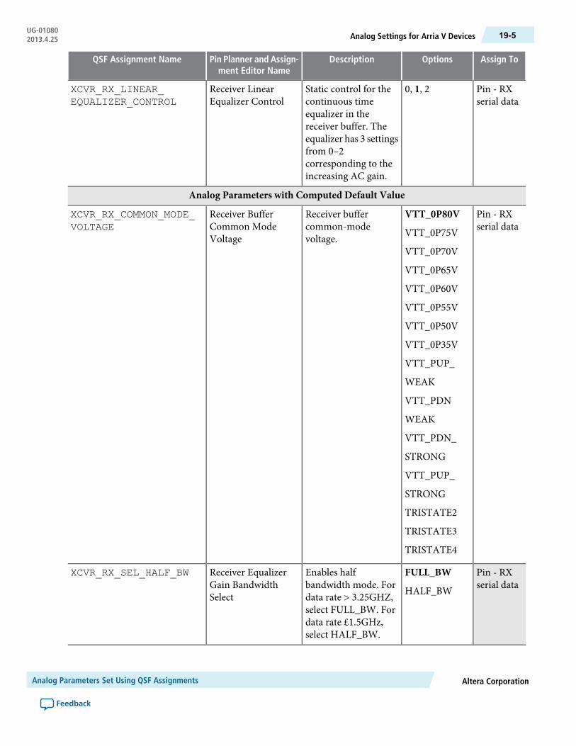
Assign ToOptionsDescriptionPin Planner and Assign-ment Editor Name
QSF Assignment Name
Pin - RXserial data
0, 1, 2Static control for thecontinuous timeequalizer in thereceiver buffer. Theequalizer has 3 settingsfrom 0–2corresponding to theincreasing AC gain.
Receiver LinearEqualizer Control
XCVR_RX_LINEAR_EQUALIZER_CONTROL
Analog Parameters with Computed Default Value
Pin - RXserial data
VTT_0P80V
VTT_0P75V
VTT_0P70V
VTT_0P65V
VTT_0P60V
VTT_0P55V
VTT_0P50V
VTT_0P35V
VTT_PUP_
WEAK
VTT_PDN
WEAK
VTT_PDN_
STRONG
VTT_PUP_
STRONG
TRISTATE2
TRISTATE3
TRISTATE4
Receiver buffercommon-modevoltage.
Receiver BufferCommon ModeVoltage
XCVR_RX_COMMON_MODE_VOLTAGE
Pin - RXserial data
FULL_BW
HALF_BW
Enables halfbandwidth mode. Fordata rate > 3.25GHZ,select FULL_BW. Fordata rate £1.5GHz,select HALF_BW.
Receiver EqualizerGain BandwidthSelect
XCVR_RX_SEL_HALF_BW
Altera CorporationAnalog Parameters Set Using QSF Assignments
Feedback
19-5Analog Settings for Arria V DevicesUG-010802013.4.25

Assign ToOptionsDescriptionPin Planner and Assign-ment Editor Name
QSF Assignment Name
Pin - RXserial data
On
Off
Enables or disables thereceiver signaldetection unit. Duringnormal operationNORMAL_SD_ON=false, otherwisePOWER_DOWN_SD=true. For thePCIe PIPE PHY.Changing from thedefault value for anyother protocol resultsin a Quartus IIcompilation error.
Receiver SignalDetection UnitEnable/Disable
XCVR_RX_SD_ENABLE
Pin - RXserial data
0–29
1
Number of parallelcycles to wait beforethe signal detect blockdeclares loss of signal.For the PCIe PIPEPHY. Changing fromthe default value forany other protocolresults in a Quartus IIcompilation error.
Receiver Cycle CountBefore Signal DetectBlock Declares LossOf Signal
XCVR_RX_SD_OFF
Pin - RXserial data
0–16
1
Number of parallelcycles to wait beforethe signal detect blockdeclares presence ofsignal. For the PCIePIPE PHY. Changingfrom the default valuefor any other protocolresults in a Quartus IIcompilation error.
Receiver Cycle CountBefore Signal DetectBlock DeclaresPresence Of Signal
XCVR_RX_SD_ON
Analog Parameters Set Using QSF AssignmentsAltera Corporation
Feedback
UG-01080Analog Settings for Arria V Devices19-6 2013.4.25

Assign ToOptionsDescriptionPin Planner and Assign-ment Editor Name
QSF Assignment Name
Pin - RXserial data
0–7
3
Specifies signaldetection voltagethreshold level. Thefollowing encodingsare defined:
• SDLV_50MV=7• SDLV_45MV=6• SDLV_40MV=5• SDLV_35MV=4• SDLV_30MV=3• SDLV_25MV=2• SDLV_20MV=1• SDLV_15MV=0
For the PCIe PIPEPHY. Changing fromthe default value forany other protocolresults in a Quartus IIcompilation error.
Receiver SignalDetection VoltageThreshold
XCVR_RX_SD_THRESHOLD
Altera CorporationAnalog Parameters Set Using QSF Assignments
Feedback
19-7Analog Settings for Arria V DevicesUG-010802013.4.25

Assign ToOptionsDescriptionPin Planner and Assign-ment Editor Name
QSF Assignment Name
Pin - TXserial data
VOLT_0P80V
VOLT_0P75V
VOLT_0P70V
VOLT_0P65V
VOLT_0P60V
VOLT_0P55V
VOLT_0P50V
VOLT_0P35V
PULL_UP
PULL_ DN
GROUNDED
PULL_UP_TO
VCCELA
TRISTATED1
TRISTATED2
TRISTATED3
TRISTATED4
Transmittercommon-mode drivervoltage.
TransmitterCommonMode Driver Voltage
XCVR_TX_COMMON_ MODE_VOLTAGE
Pin - TXserial data
0–31Specifies the firstpost-tap setting value.
TransmitterPreemphasis FirstPost-Tap
XCVR_TX_PRE_EMP_1ST_POST_TAP
Pin - TXserial data
TRUE
FALSE
Enables or disables thereceiver detectorcircuit at thetransmitter.
Transmitter's ReceiverDetect Block Enable
XCVR_TX_RX_DET_ENABLE
Pin - TXserial data
0–15Sets the mode forreceiver detect block.
Transmitter's ReceiverDetect Block Mode
XCVR_TX_RX_DET_MODE
Pin - TXserial data
0–63Differential outputvoltage setting. Thevalues aremonotonicallyincreasing with thedriver main tapcurrent strength.
TransmitterDifferential OutputVoltage
XCVR_RX_VOD
Analog Parameters Set Using QSF AssignmentsAltera Corporation
Feedback
UG-01080Analog Settings for Arria V Devices19-8 2013.4.25

Assign ToOptionsDescriptionPin Planner and Assign-ment Editor Name
QSF Assignment Name
Pin - TXserial data
DYNAMIC_CTL
RAM_CTL
When set toDYNAMIC_ CTL, thePCS block controls theVODandpreemphasisare controlled by otherassignments. such asXCVR_TX_PRE_EMP_1ST_POST_TAP.
TransmitterVOD/PreemphasisControl
XCVR_TX_VOD_PRE_EMP_CTRL_SRC
For more information about the Pin Planner, refer to About the Pin Planner in Quartus II Help. For moreinformation about the Assignment Editor, refer to About the Assignment Editor in Quartus II Help.
For more information about Quartus II Settings, refer to Quartus II Settings File Manual.
Related InformationPCI Express Card Electromechanical Specification Rev. 2.0
About the Pin Planner
About the Assignment Editor
Quartus II Settings File Manual
Analog Settings for Arria V GZ DevicesThis section lists the analog parameters for Arria V GZ devices whose original values are place holders forthe values thatmatch your electrical board specification. In the following table, the default value of an analogparameter is shown in bold type. The parameters are listed in alphabetical order.
Table 19-3: Transceiver and PLL Assignments for Arria V GZ Devices
Assign ToOptionsDescriptionPin Planner andAssignment Editor
Name
QSF Assignment Name
Pin - TX& RXserialdata
85_Ohms
100_Ohms
120_Ohms
150_Ohms
External_Resistor
Specifies the intended on-chiptermination value for thespecified transceiver pin. UseExternal Resistor if you intend touse off-chip termination.
Transceiver I/OPin Termination
XCVR_IO_PIN_TERMINATION
Altera CorporationAnalog Parameters Set Using QSF Assignments
Feedback
19-9Analog Settings for Arria V GZ DevicesUG-010802013.4.25
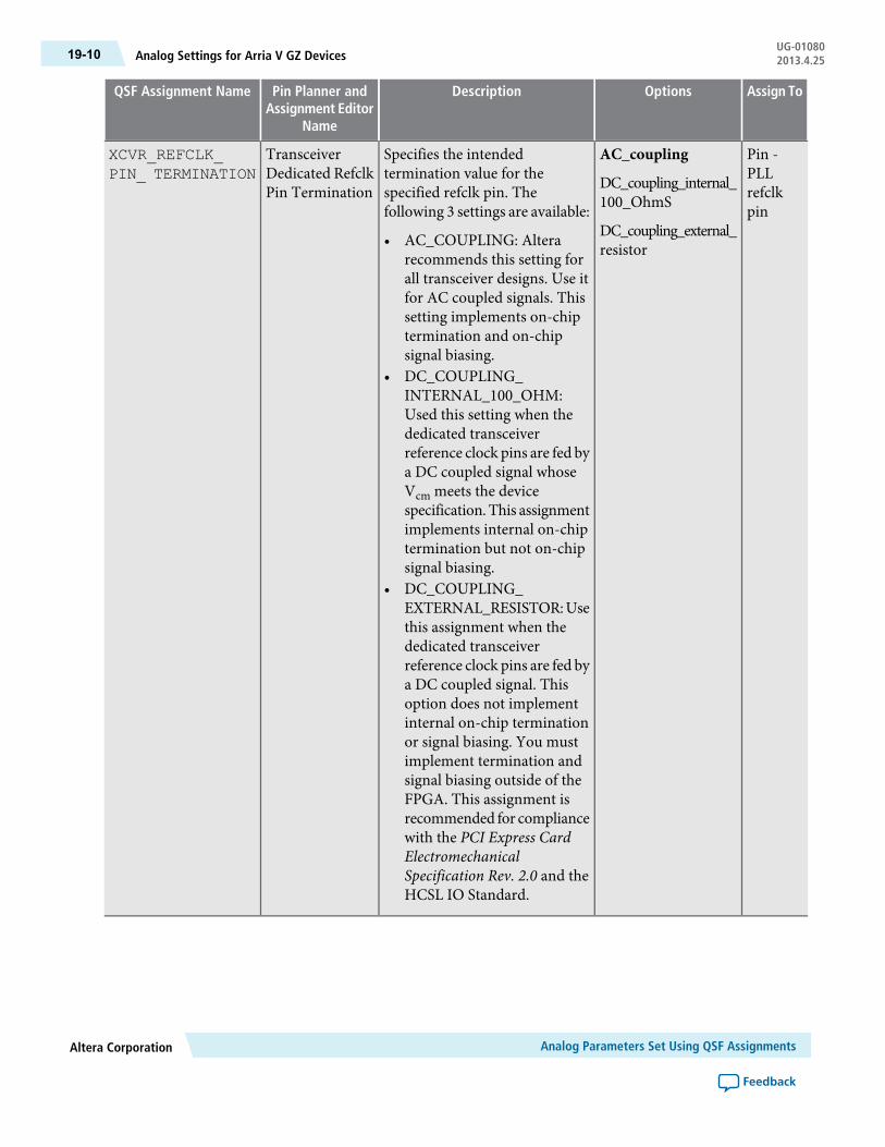
Assign ToOptionsDescriptionPin Planner andAssignment Editor
Name
QSF Assignment Name
Pin -PLLrefclkpin
AC_coupling
DC_coupling_internal_100_OhmS
DC_coupling_external_resistor
Specifies the intendedtermination value for thespecified refclk pin. Thefollowing 3 settings are available:
• AC_COUPLING: Alterarecommends this setting forall transceiver designs. Use itfor AC coupled signals. Thissetting implements on-chiptermination and on-chipsignal biasing.
• DC_COUPLING_INTERNAL_100_OHM:Used this setting when thededicated transceiverreference clock pins are fed bya DC coupled signal whoseVcm meets the devicespecification. This assignmentimplements internal on-chiptermination but not on-chipsignal biasing.
• DC_COUPLING_EXTERNAL_RESISTOR:Usethis assignment when thededicated transceiverreference clock pins are fed bya DC coupled signal. Thisoption does not implementinternal on-chip terminationor signal biasing. You mustimplement termination andsignal biasing outside of theFPGA. This assignment isrecommended for compliancewith the PCI Express CardElectromechanicalSpecification Rev. 2.0 and theHCSL IO Standard.
TransceiverDedicated RefclkPin Termination
XCVR_REFCLK_PIN_ TERMINATION
Analog Parameters Set Using QSF AssignmentsAltera Corporation
Feedback
UG-01080Analog Settings for Arria V GZ Devices19-10 2013.4.25
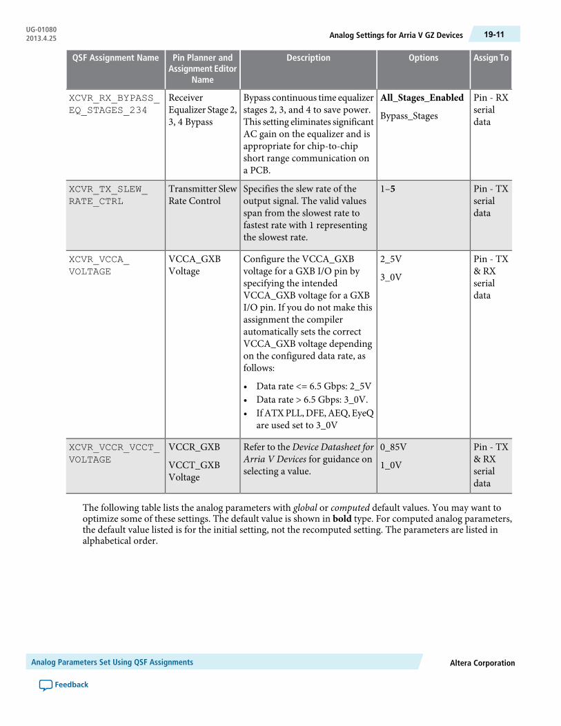
Assign ToOptionsDescriptionPin Planner andAssignment Editor
Name
QSF Assignment Name
Pin - RXserialdata
All_Stages_Enabled
Bypass_Stages
Bypass continuous time equalizerstages 2, 3, and 4 to save power.This setting eliminates significantAC gain on the equalizer and isappropriate for chip-to-chipshort range communication ona PCB.
ReceiverEqualizer Stage 2,3, 4 Bypass
XCVR_RX_BYPASS_EQ_STAGES_234
Pin - TXserialdata
1–5Specifies the slew rate of theoutput signal. The valid valuesspan from the slowest rate tofastest rate with 1 representingthe slowest rate.
Transmitter SlewRate Control
XCVR_TX_SLEW_RATE_CTRL
Pin - TX& RXserialdata
2_5V
3_0V
Configure the VCCA_GXBvoltage for a GXB I/O pin byspecifying the intendedVCCA_GXB voltage for a GXBI/O pin. If you do not make thisassignment the compilerautomatically sets the correctVCCA_GXB voltage dependingon the configured data rate, asfollows:
• Data rate <= 6.5 Gbps: 2_5V• Data rate > 6.5 Gbps: 3_0V.• If ATXPLL,DFE,AEQ, EyeQ
are used set to 3_0V
VCCA_GXBVoltage
XCVR_VCCA_VOLTAGE
Pin - TX& RXserialdata
0_85V
1_0V
Refer to the Device Datasheet forArria V Devices for guidance onselecting a value.
VCCR_GXB
VCCT_GXBVoltage
XCVR_VCCR_VCCT_VOLTAGE
The following table lists the analog parameters with global or computed default values. You may want tooptimize some of these settings. The default value is shown in bold type. For computed analog parameters,the default value listed is for the initial setting, not the recomputed setting. The parameters are listed inalphabetical order.
Altera CorporationAnalog Parameters Set Using QSF Assignments
Feedback
19-11Analog Settings for Arria V GZ DevicesUG-010802013.4.25
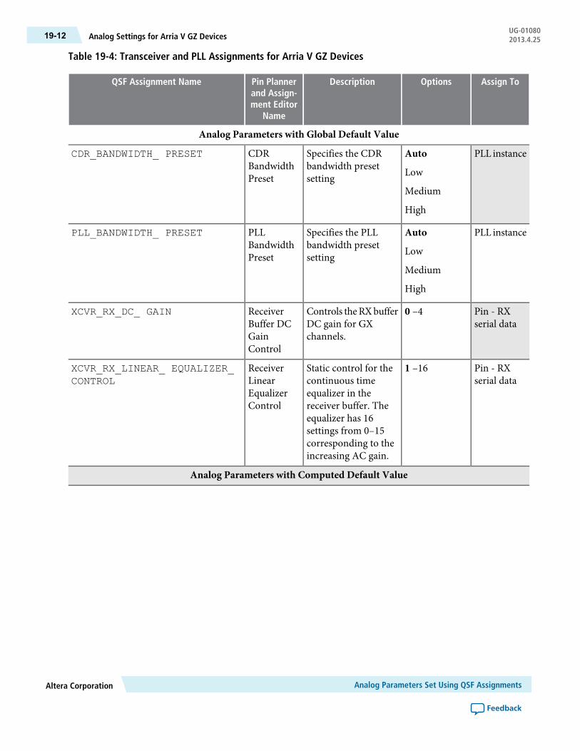
Table 19-4: Transceiver and PLL Assignments for Arria V GZ Devices
Assign ToOptionsDescriptionPin Plannerand Assign-ment Editor
Name
QSF Assignment Name
Analog Parameters with Global Default Value
PLL instanceAuto
Low
Medium
High
Specifies the CDRbandwidth presetsetting
CDRBandwidthPreset
CDR_BANDWIDTH_ PRESET
PLL instanceAuto
Low
Medium
High
Specifies the PLLbandwidth presetsetting
PLLBandwidthPreset
PLL_BANDWIDTH_ PRESET
Pin - RXserial data
0 –4Controls theRXbufferDC gain for GXchannels.
ReceiverBuffer DCGainControl
XCVR_RX_DC_ GAIN
Pin - RXserial data
1 –16Static control for thecontinuous timeequalizer in thereceiver buffer. Theequalizer has 16settings from 0–15corresponding to theincreasing AC gain.
ReceiverLinearEqualizerControl
XCVR_RX_LINEAR_ EQUALIZER_CONTROL
Analog Parameters with Computed Default Value
Analog Parameters Set Using QSF AssignmentsAltera Corporation
Feedback
UG-01080Analog Settings for Arria V GZ Devices19-12 2013.4.25

Assign ToOptionsDescriptionPin Plannerand Assign-ment Editor
Name
QSF Assignment Name
Pin - RXserial data
VTT_0P80V
VTT_0P75V
VTT_0P70V
VTT_0P65V
VTT_0P60V
VTT_0P55V
VTT_0P50V
VTT_0P35V
VTT_PUP
_WEAK
VTT_PDN
WEAK
TRISTATE1
VTT_PDN_
STRONG
VTT_PUP_
STRONG
TRISTATE2
TRISTATE3
TRISTATE4
Receiver buffercommon-modevoltage.
ReceiverBufferCommonModeVoltage
XCVR_RX_COMMON_ MODE_VOLTAGE_
Pin - RXserial data
TRUE
FALSE
If enabled equalizergain control is drivenby the PCS block forPCI Express. Ifdisabled equalizer gaincontrol is determinedby the XCVR_RX_LINEAR_EQUALIZER_SETTINGassignment.
ReceiverLinearEqualizerControl(PCIExpress)
XCVR_RX_ENABLE_ LINEAR_EQUALIZER_ PCIEMODE
Altera CorporationAnalog Parameters Set Using QSF Assignments
Feedback
19-13Analog Settings for Arria V GZ DevicesUG-010802013.4.25

Assign ToOptionsDescriptionPin Plannerand Assign-ment Editor
Name
QSF Assignment Name
Pin - RXserial data
FULL
HALF
Sets the gain peakingfrequency for theequalizer. Fordata-rates of less than6.5Gbps set to HALF.For higher data-ratesset to FULL.
ReceiverEqualizerGainBandwidthSelect
XCVR_RX_SEL_HALF_BW
Pin - RXserial data
On
Off
Enables or disables thereceiver signaldetection unit. For thePCIe PIPE PHY.Changing from thedefault value for anyother protocol resultsin a Quartus IIcompilation error.
ReceiverSignalDetectionUnitEnable/Disable
XCVR_RX_SD_ENABLE
Pin - RXserial data
0–29Number of parallelcycles to wait beforethe signal detect blockdeclares loss of signal.For the PCIe PIPEPHY. Changing fromthe default value forany other protocolresults in a Quartus IIcompilation error.
ReceiverCycle CountBeforeSignalDetect BlockDeclaresLoss OfSignal
XCVR_RX_SD_OFF
Pin - RXserial data
0–16Number of parallelcycles to wait beforethe signal detect blockdeclares presence ofsignal. For the PCIePIPE PHY. Changingfrom the default valuefor any other protocolresults in a Quartus IIcompilation error.
ReceiverCycle CountBeforeSignalDetect BlockDeclaresPresence OfSignal
XCVR_RX_SD_ON
Analog Parameters Set Using QSF AssignmentsAltera Corporation
Feedback
UG-01080Analog Settings for Arria V GZ Devices19-14 2013.4.25

Assign ToOptionsDescriptionPin Plannerand Assign-ment Editor
Name
QSF Assignment Name
Pin - RXserial data
0–7Specifies signaldetection voltagethreshold level. Thefollowing encodingsare defined:
• SDLV_50MV=7• SDLV_45MV=6• SDLV_40MV=5• SDLV_35MV=4• SDLV_30MV=3• SDLV_25MV=2• SDLV_20MV=1• SDLV_15MV=0
For the PCIe PIPEPHY. Changing fromthe default value forany other protocolresults in a Quartus IIcompilation error.
ReceiverSignalDetectionVoltageThreshold
XCVR_RX_SD_ THRESHOLD
Altera CorporationAnalog Parameters Set Using QSF Assignments
Feedback
19-15Analog Settings for Arria V GZ DevicesUG-010802013.4.25
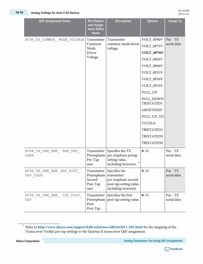
Assign ToOptionsDescriptionPin Plannerand Assign-ment Editor
Name
QSF Assignment Name
Pin - TXserial data
VOLT_0P80V
VOLT_0P75V
VOLT_0P70V
VOLT_0P65V
VOLT_0P60V
VOLT_0P55V
VOLT_0P50V
VOLT_0P35V
PULL_UP
PULL_DOWNTRISTATED1
GROUNDED
PULL_UP_TO
VCCELA
TRISTATED2
TRISTATED3
TRISTATED4
Transmittercommon-mode drivervoltage.
TransmitterCommonModeDriverVoltage
XCVR_TX_COMMON_ MODE_VOLTAGE
Pin - TXserial data
0–31.Specifies the TXpre-emphasis pretapsetting value,including inversion. 7
TransmitterPreemphasisPre-Tapuser
XCVR_TX_PRE_EMP_ PRE_TAP_USER
Pin - TXserial data
0–31Specifies thetransmitterpre-emphasis secondpost-tap setting value,including inversion.
TransmitterPreemphasisSecondPost-Tapuser
XCVR_TX_PRE_EMP_2ND_POST_TAP_USER
Pin - TXserial data
0–31Specifies the firstpost-tap setting value.
TransmitterPreemphasisFirstPost-Tap
XCVR_TX_PRE_EMP_ 1ST_POST_TAP
7 Refer to http://www.altera.com/support/kdb/solutions/rd02262013_691.html for the mapping of theTransceiver Toolkit pre-tap settings to the Quartus II transceiver QSF assignment.
Analog Parameters Set Using QSF AssignmentsAltera Corporation
Feedback
UG-01080Analog Settings for Arria V GZ Devices19-16 2013.4.25

Assign ToOptionsDescriptionPin Plannerand Assign-ment Editor
Name
QSF Assignment Name
Pin - TXserial data
0–15Specifies the secondpost-tap setting value.8
TransmitterPreemphasisSecondPost-Tap
XCVR_TX_PRE_EMP_ 2ND_POST_TAP
Pin - TXserial data
TRUE
FALSE
Inverts the transmitterpre-emphasis 2ndposttap. 8
TransmitterPreemphasisSecond TapInvert
XCVR_TX_PRE_EMP_ INV_2ND_TAP
Pin - TXserial data
TRUE
FALSE
Inverts the transmitterpre-emphasis pre-tap.7
TransmitterPreemphasisPre TapInvert
XCVR_TX_PRE_EMP_ INV_PRE_TAP
Pin - TXserial data
0–15Specifies the pre-tappre-emphasis setting.
TransmitterPreemphasisPre Tap
XCVR_TX_PRE_EMP_PRE_TAP
Pin - TXserial data
TRUE
FALSE
Enables or disables thereceiver detectorcircuit at thetransmitter.
Transmitter'sReceiverDetect BlockEnable
XCVR_TX_RX_DET_ ENABLE
Pin - TXserial data
0–15Sets the mode forreceiver detect block.
Transmitter'sReceiverDetect BlockMode
XCVR_TX_RX_DET_ MODE
Pin - TXserial data
RX_DET_QPI_OUT
RX_DET_PCIE_OUT
Determines QPI orPCI Express mode forthe Receiver Detectblock.
Transmitter'sReceiverDetect BlockQPI/PCIExpressControl
XCVR_TX_RX_DET_ OUTPUT_SEL
Pin - TXserial data
0–63
50
Differential outputvoltage setting. Thevalues aremonotonicallyincreasing with thedriver main tapcurrent strength.
TransmitterDifferentialOutputVoltage
XCVR_TX_VOD
8 Refer to http://www.altera.com/support/kdb/solutions/rd02272013_545.html for the mapping of theTransceiver Toolkit pre-tap settings to this setting.
Altera CorporationAnalog Parameters Set Using QSF Assignments
Feedback
19-17Analog Settings for Arria V GZ DevicesUG-010802013.4.25

Assign ToOptionsDescriptionPin Plannerand Assign-ment Editor
Name
QSF Assignment Name
Pin - TXserial data
DYNAMIC_CTL
RAM_CTL
When set toDYNAMIC_CTL, thePCS block controls theVOD and preemphasiscoefficients for PCIExpress. When thisassignment is set toRAM_CTL the VODand preemphasis arecontrolled by otherassignments, such asXCVR_TX_PRE_EMP_ 1ST_POST_TAP
TransmitterVOD/PreemphasisControl
XCVR_TX_VOD_PRE_ EMP_CTRL_SRC
For more information about the Pin Planner, refer to About the Pin Planner in Quartus II Help. For moreinformation about the Assignment Editor, refer to About the Assignment Editor in Quartus II Help.
For more information about Quartus II Settings, refer to Quartus II Settings File Manual.
Related InformationPCI Express Card Electromechanical Specification Rev. 2.0
Device Datasheet for Arria V Devices
About the Pin Planner
About the Assignment Editor
Quartus II Settings File Manual
Analog Settings for Cyclone V DevicesThis section lists the analog parameters for Cyclone V devices whose original values are place holders forthe values thatmatch your electrical board specification. In the following table, the default value of an analogparameter is shown in bold type. The parameters are listed in alphabetical order.
Analog Parameters Set Using QSF AssignmentsAltera Corporation
Feedback
UG-01080Analog Settings for Cyclone V Devices19-18 2013.4.25
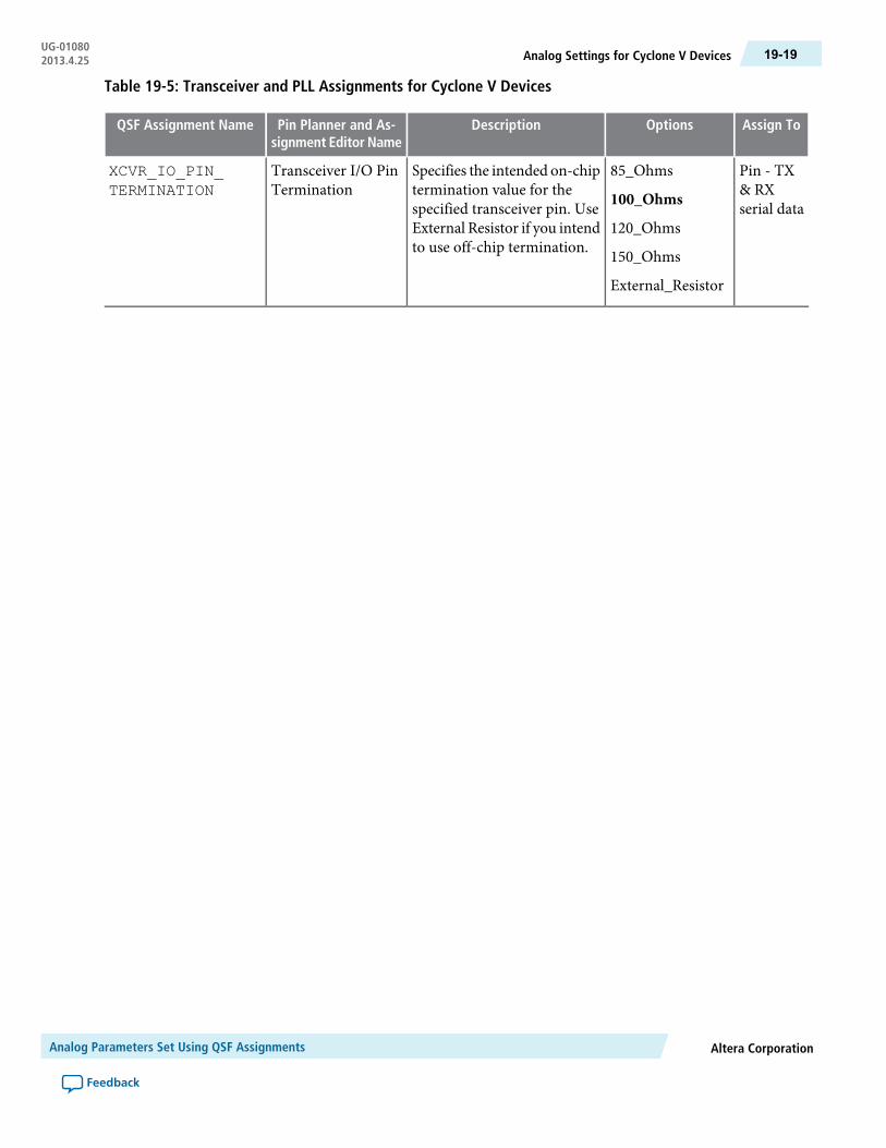
Table 19-5: Transceiver and PLL Assignments for Cyclone V Devices
Assign ToOptionsDescriptionPin Planner and As-signment Editor Name
QSF Assignment Name
Pin - TX& RXserial data
85_Ohms
100_Ohms
120_Ohms
150_Ohms
External_Resistor
Specifies the intended on-chiptermination value for thespecified transceiver pin. UseExternal Resistor if you intendto use off-chip termination.
Transceiver I/O PinTermination
XCVR_IO_PIN_TERMINATION
Altera CorporationAnalog Parameters Set Using QSF Assignments
Feedback
19-19Analog Settings for Cyclone V DevicesUG-010802013.4.25

Assign ToOptionsDescriptionPin Planner and As-signment Editor Name
QSF Assignment Name
Pin - PLLrefclk pin
AC_coupling
DC_coupling_internal_100_OhmS
DC_coupling_external_resistor
Specifies the intendedtermination value for thespecified refclk pin. Thefollowing 3 settings areavailable:
• AC_COUPLING: Alterarecommends this settingfor all transceiver designs.Use it for AC coupledsignals. This settingimplements on-chiptermination and on-chipsignal biasing.
• DC_COUPLING_INTERNAL_100_OHM:Used this setting when thededicated transceiverreference clock pins are fedby a DC coupled signalwhose Vcm meets thedevice specification. Thisassignment implementsinternal on-chiptermination but noton-chip signal biasing.
• DC_COUPLING_EXTERNAL_RESISTOR:Use this assignment whenthe dedicated transceiverreference clock pins are fedby a DC coupled signal.This option does notimplement internalon-chip termination orsignal biasing. You mustimplement terminationand signal biasing outsideof the FPGA. Thisassignment isrecommended forcompliance with the PCIExpress CardElectromechanicalSpecification Rev. 2.0 andthe HCSL IO Standard.
TransceiverDedicatedRefclk PinTermination
XCVR_REFCLK_PIN_TERMINATION
Analog Parameters Set Using QSF AssignmentsAltera Corporation
Feedback
UG-01080Analog Settings for Cyclone V Devices19-20 2013.4.25

Assign ToOptionsDescriptionPin Planner and As-signment Editor Name
QSF Assignment Name
Pin - TXserial data
1–5Specifies the slew rate of theoutput signal. The followingencodings are defined:
• 1: SLEW_160PS• 2: SLEW_90PS• 3: SLEW_50PS• 4: SLEW_30PS• 5: SLEW_15PS
Transmitter SlewRate Control
XCVR_TX_SLEW_RATE_CTRL
Pin - TX& RXserial data
1_1V
1_2V
Configures the VCCE_GXBvoltage for an GXB I/O pin byspecifying the intended supplyvoltages for a GXB I/O pin.
VCCT_GXBVoltageXCVR_VCCR_ VCCT_VOLTAGE
The following table lists the analog parameters with global or computed default values. You may want tooptimize some of these settings. The default value is shown in bold type. For computed analog parameters,the default value listed is for the initial setting, not the recomputed setting. The parameters are listed inalphabetical order.
Table 19-6: Transceiver and PLL Assignments for Cyclone V Devices
Assign ToOptionsDescriptionPin Planner andAssignment Editor
Name
QSF Assignment Name
Analog Parameters with Global Default Value
PLLinstance
Auto
Low
Medium
High
Specifies the CDRbandwidth preset setting
CDR BandwidthPreset
CDR_BANDWIDTH_PRESET
PLLinstance
Auto
Low
Medium
High
Specifies the PLLbandwidth preset setting
PLL BandwidthPreset
PLL_BANDWIDTH_PRESET
Pin - RXserial data
0 –1Controls the amount of astage receive-buffer DCgain.
Receiver BufferDC Gain Control
XCVR_RX_DC_GAIN
Altera CorporationAnalog Parameters Set Using QSF Assignments
Feedback
19-21Analog Settings for Cyclone V DevicesUG-010802013.4.25

Assign ToOptionsDescriptionPin Planner andAssignment Editor
Name
QSF Assignment Name
Pin - RXserial data
0, 1, 2Static control for thecontinuous time equalizerin the receiver buffer. Theequalizer has 3 settingsfrom0–2 corresponding tothe increasing AC gain.
Receiver LinearEqualizerControl
XCVR_RX_LINEAR_EQUALIZER_CONTROL
Analog Parameters with Computed Default Value
VTT_0P80V
VTT_0P75V
VTT_0P70V
VTT_0P65V
VTT_0P60V
VTT_0P55V
VTT_0P50V
VTT_0P35V
VTT_PUP
_WEAK
VTT_PDN
WEAK
TRISTATE1
VTT_PDN_
STRONG
VTT_PUP_
STRONG
TRISTATE2
TRISTATE3
TRISTATE4
Receiver buffercommon-mode voltage.
Receiver BufferCommon ModeVoltage
XCVR_RX_COMMON_MODE_VOLTAGE_
Pin - RXserial data
FULL_BW
HALF_BW
Enables half bandwidthmode. For data rate >3.25GHZ, selectFULL_BW. For data rate£1.5GHz, selectHALF_BW.
ReceiverEqualizer GainBandwidth Select
XCVR_RX_SEL_HALF_BW
Analog Parameters Set Using QSF AssignmentsAltera Corporation
Feedback
UG-01080Analog Settings for Cyclone V Devices19-22 2013.4.25

Assign ToOptionsDescriptionPin Planner andAssignment Editor
Name
QSF Assignment Name
Pin - RXserial data
On
Off
Enables or disables thereceiver signal detectionunit. During normaloperation NORMAL_SD_ON=false, otherwisePOWER_DOWN_SD=true.For the PCIe PIPE PHY.Changing from the defaultvalue for any otherprotocol results in aQuartus II compilationerror.
Receiver SignalDetection UnitEnable/Disable
XCVR_RX_SD_ENABLE
Pin - RXserial data
0–29Number of parallel cyclesto wait before the signaldetect block declares lossof signal. For the PCIePIPEPHY.Changing fromthe default value for anyother protocol results in aQuartus II compilationerror.
Receiver CycleCount BeforeSignal DetectBlock DeclaresLoss Of Signal
XCVR_RX_SD_OFF
Pin - RXserial data
0–16Number of parallel cyclesto wait before the signaldetect block declarespresence of signal. For thePCIe PIPEPHY.Changingfrom the default value forany other protocol resultsin aQuartus II compilationerror.
Receiver CycleCount BeforeSignal DetectBlock DeclaresPresence OfSignal
XCVR_RX_SD_ON
Altera CorporationAnalog Parameters Set Using QSF Assignments
Feedback
19-23Analog Settings for Cyclone V DevicesUG-010802013.4.25

Assign ToOptionsDescriptionPin Planner andAssignment Editor
Name
QSF Assignment Name
Pin - RXserial data
0–7
3
Specifies signal detectionvoltage threshold level. Thefollowing encodings aredefined:
• SDLV_50MV=7• SDLV_45MV=6• SDLV_40MV=5• SDLV_35MV=4• SDLV_30MV=3• SDLV_25MV=2• SDLV_20MV=1• SDLV_15MV=0
For the PCIe PIPE PHY.Changing from the defaultvalue for any otherprotocol results in aQuartus II compilationerror.
Receiver SignalDetectionVoltageThreshold
XCVR_RX_SD_THRESHOLD
Pin - TXserial data
VOLT_0P80V
VOLT_0P75V
VOLT_0P70V
VOLT_0P65V
VOLT_0P60V
VOLT_0P55V
VOLT_0P50V
VOLT_0P35V
PULL_UP
PULL_DOWNTRISTATED1
GROUNDED
PULL_UP_TO
VCCELA
TRISTATED2
TRISTATED3
TRISTATED4
Transmittercommon-mode drivervoltage.
TransmitterCommon ModeDriver Voltage
XCVR_TX_COMMON_MODE_VOLTAGE
Analog Parameters Set Using QSF AssignmentsAltera Corporation
Feedback
UG-01080Analog Settings for Cyclone V Devices19-24 2013.4.25

Assign ToOptionsDescriptionPin Planner andAssignment Editor
Name
QSF Assignment Name
Pin - TXserial data
0–31Specifies the first post-tapsetting value.
TransmitterPreemphasis FirstPost-Tap
XCVR_TX_PRE_EMP _1ST_POST_TAP
Pin - TXserial data
TRUE
FALSE
Enables or disables thereceiver detector circuit atthe transmitter.
Transmitter'sReceiver DetectBlock Enable
XCVR_TX_RX_DET_ENABLE
Pin - TXserial data
0–15Sets the mode for receiverdetect block.
Transmitter'sReceiver DetectBlock Mode
XCVR_TX_RX_DET_MODE
Pin - TXserial data
0–63Differential output voltagesetting. The values aremonotonically increasingwith the driver main tapcurrent strength.
TransmitterDifferentialOutput Voltage
XCVR_TX_VOD
Pin - TXserial data
DYNAMIC_CTL
RAM_CTL
When set to DYNAMIC_CTL, the PCS blockcontrols the VOD andpreemphasis are controlledby other assignments. suchas XCVR_TX_PRE_EMP_1ST_POST_TAP.
TransmitterVOD/PreemphasisControl
XCVR_TX_VOD_PRE_EMP_CTRL_SRC
For more information about the Pin Planner, refer to About the Pin Planner in Quartus II Help. For moreinformation about the Assignment Editor, refer to About the Assignment Editor in Quartus II Help.
For more information about Quartus II Settings, refer to Quartus II Settings File Manual.
Related InformationPCI Express Card Electromechanical Specification Rev. 2.0
About the Pin Planner
About the Assignment Editor
Quartus II Settings File Manual
Analog Settings for Stratix V DevicesThis section lists the analog parameters for Stratix V devices whose original values are place holders for thevalues that match your electrical board specification. In the following table, the default value of an analogparameter is shown in bold type. The parameters are listed in alphabetical order.
Altera CorporationAnalog Parameters Set Using QSF Assignments
Feedback
19-25Analog Settings for Stratix V DevicesUG-010802013.4.25
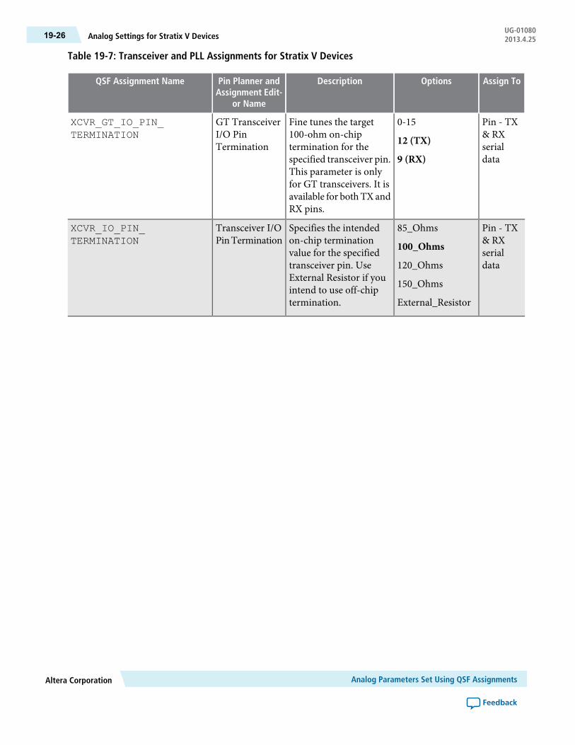
Table 19-7: Transceiver and PLL Assignments for Stratix V Devices
Assign ToOptionsDescriptionPin Planner andAssignment Edit-
or Name
QSF Assignment Name
Pin - TX& RXserialdata
0-15
12 (TX)
9 (RX)
Fine tunes the target100-ohm on-chiptermination for thespecified transceiver pin.This parameter is onlyfor GT transceivers. It isavailable for bothTX andRX pins.
GT TransceiverI/O PinTermination
XCVR_GT_IO_PIN_TERMINATION
Pin - TX& RXserialdata
85_Ohms
100_Ohms
120_Ohms
150_Ohms
External_Resistor
Specifies the intendedon-chip terminationvalue for the specifiedtransceiver pin. UseExternal Resistor if youintend to use off-chiptermination.
Transceiver I/OPinTermination
XCVR_IO_PIN_TERMINATION
Analog Parameters Set Using QSF AssignmentsAltera Corporation
Feedback
UG-01080Analog Settings for Stratix V Devices19-26 2013.4.25

Assign ToOptionsDescriptionPin Planner andAssignment Edit-
or Name
QSF Assignment Name
Pin - PLLrefclk pin
AC_coupling
DC_coupling_internal_100_OhmS
DC_coupling_external_resistor
TransceiverDedicatedRefclk PinTermination
XCVR_REFCLK_PIN_TERMINATION
Altera CorporationAnalog Parameters Set Using QSF Assignments
Feedback
19-27Analog Settings for Stratix V DevicesUG-010802013.4.25

Assign ToOptionsDescriptionPin Planner andAssignment Edit-
or Name
QSF Assignment Name
Specifies the intendedtermination value for thespecified refclk pin. Thefollowing 3 settings areavailable:
• AC_COUPLING:Altera recommendsthis setting for alltransceiver designs.Use it for AC coupledsignals. This settingimplements on-chiptermination andon-chip signalbiasing.
• DC_COUPLING_INTERNAL_100_OHM:Used this settingwhen the dedicatedtransceiver referenceclock pins are fed bya DC coupled signalwhose Vcm meets thedevice specification.This assignmentimplements internalon-chip terminationbut not on-chip signalbiasing.
• DC_COUPLING_EXTERNAL_RESISTOR:Use this assignmentwhen the dedicatedtransceiver referenceclock pins are fed bya DC coupled signal.This option does notimplement internalon-chip terminationor signal biasing. Youmust implementtermination andsignal biasing outsideof the FPGA. This
Analog Parameters Set Using QSF AssignmentsAltera Corporation
Feedback
UG-01080Analog Settings for Stratix V Devices19-28 2013.4.25

Assign ToOptionsDescriptionPin Planner andAssignment Edit-
or Name
QSF Assignment Name
assignment isrecommended forcompliance with thePCI Express CardElectromechanicalSpecification Rev. 2.0and the HCSL IOStandard.
Pin - RXserialdata
All_Stages_Enabled
Bypass_Stages
Bypass continuous timeequalizer stages 2, 3, and4 to save power. Thissetting eliminatessignificant AC gain onthe equalizer and isappropriate forchip-to-chip short rangecommunication on aPCB.
ReceiverEqualizer Stage2, 3, 4 Bypass
XCVR_RX_BYPASS_EQ_STAGES_234
Pin - TXserialdata
1–5Specifies the slew rate ofthe output signal. Thevalid values span fromthe slowest rate to fastestrate with 1 representingthe slowest rate.
TransmitterSlew RateControl
XCVR_TX_SLEW_ RATE_CTRL
Pin - TX& RXserialdata
2_5V
3_0V
Configure theVCCA_GXB voltage fora GXB I/O pin byspecifying the intendedVCCA_GXB voltage fora GXB I/O pin. If you donotmake this assignmentthe compilerautomatically sets thecorrect VCCA_GXBvoltage depending on theconfigured data rate, asfollows:
• Data rate <= 6.5Gbps: 2_5V
• Data rate > 6.5 Gbps:3_0V.
VCCA_GXBVoltage
XCVR_VCCA_VOLTAGE
Altera CorporationAnalog Parameters Set Using QSF Assignments
Feedback
19-29Analog Settings for Stratix V DevicesUG-010802013.4.25

Assign ToOptionsDescriptionPin Planner andAssignment Edit-
or Name
QSF Assignment Name
Pin - TX& RXserialdata
0_85V
1_0V
Refer to the DeviceDatasheet for Stratix VDevices for guidance onselecting a value.
VCCR_GXB
VCCT_GXBVoltage
XCVR_VCCR_VCCT_VOLTAGE
The following table lists the analog parameters with global or computed default values. You may want tooptimize some of these settings. The default value is shown in bold type. For computed analog parameters,the default value listed is for the initial setting, not the recomputed setting. The parameters are listed inalphabetical order.
Table 19-8: Transceiver and PLL Assignments for Stratix V Devices
AssignTo
OptionsDescriptionPin Planner and Assign-ment Editor Name
QSF Assignment Name
Analog Parameters with Global Default Value
PLLinstance
Auto
Low
Medium
High
Specifies the CDRbandwidth presetsetting
CDRBandwidthPresetCDR_BANDWIDTH_PRESET
PLLinstance
Auto
Low
Medium
High
Specifies the PLLbandwidth presetsetting
PLL Bandwidth PresetPLL_BANDWIDTH_PRESET
Pin - RXserialdata
0 –19
8
Controls the RX bufferDC gain forGTchannels.
Receiver Buffer DCGain Control
XCVR_GT_RX_DC_GAIN
Pin - RXserialdata
0 –4Controls the RX bufferDC gain for GXchannels.
Receiver Buffer DCGain Control
XCVR_RX_DC_GAIN
Pin - RXserialdata
1 –16Static control for thecontinuous timeequalizer in thereceiver buffer. Theequalizer has 16settings from 0–15corresponding to theincreasing AC gain.
Receiver LinearEqualizer Control
XCVR_RX_LINEAR_EQUALIZER_CONTROL
Analog Parameters with Computed Default Value
Analog Parameters Set Using QSF AssignmentsAltera Corporation
Feedback
UG-01080Analog Settings for Stratix V Devices19-30 2013.4.25
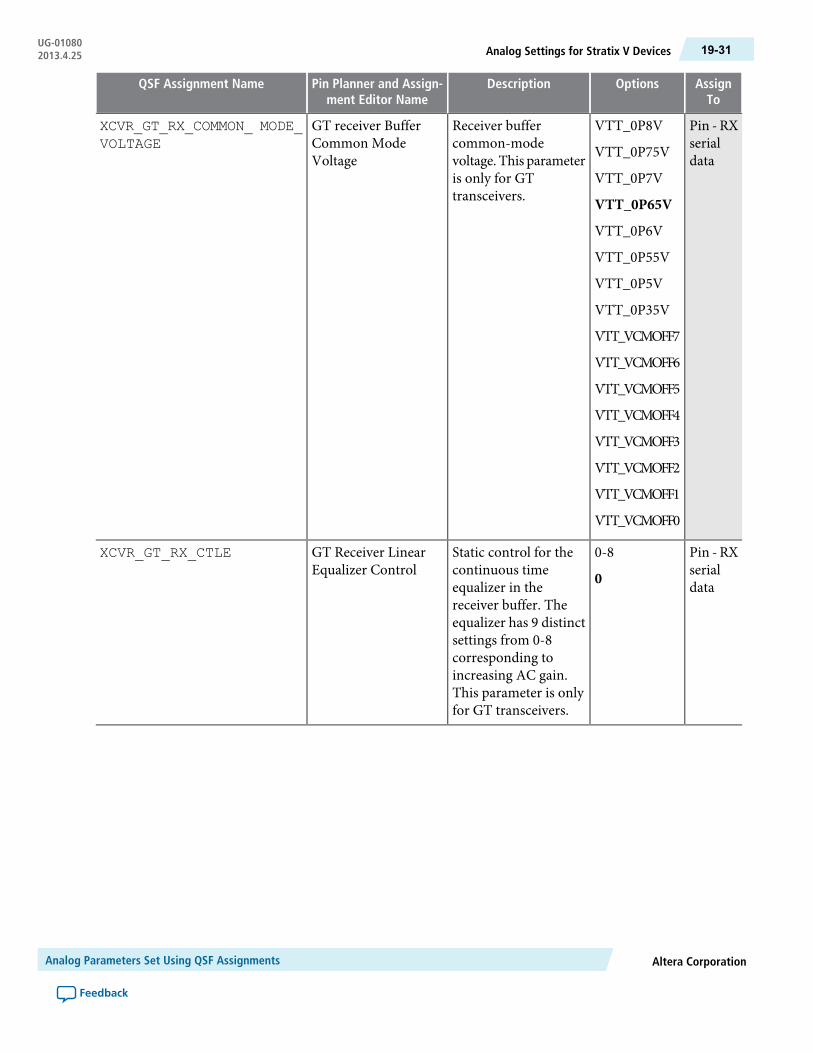
AssignTo
OptionsDescriptionPin Planner and Assign-ment Editor Name
QSF Assignment Name
Pin - RXserialdata
VTT_0P8V
VTT_0P75V
VTT_0P7V
VTT_0P65V
VTT_0P6V
VTT_0P55V
VTT_0P5V
VTT_0P35V
VTT_VCMOFF7
VTT_VCMOFF6
VTT_VCMOFF5
VTT_VCMOFF4
VTT_VCMOFF3
VTT_VCMOFF2
VTT_VCMOFF1
VTT_VCMOFF0
Receiver buffercommon-modevoltage. This parameteris only for GTtransceivers.
GT receiver BufferCommon ModeVoltage
XCVR_GT_RX_COMMON_ MODE_VOLTAGE
Pin - RXserialdata
0-8
0
Static control for thecontinuous timeequalizer in thereceiver buffer. Theequalizer has 9 distinctsettings from 0-8corresponding toincreasing AC gain.This parameter is onlyfor GT transceivers.
GT Receiver LinearEqualizer Control
XCVR_GT_RX_CTLE
Altera CorporationAnalog Parameters Set Using QSF Assignments
Feedback
19-31Analog Settings for Stratix V DevicesUG-010802013.4.25

AssignTo
OptionsDescriptionPin Planner and Assign-ment Editor Name
QSF Assignment Name
Pin - TXserialdata
VOLT_0P80V
VOLT_0P75V
VOLT_0P70V
VOLT_0P65V
VOLT_0P60V
VOLT_0P55V
VOLT_0P50V
VOLT_0P35V
PULL_UP
PULL_DN
TRISTATED1
GROUNDED
PULL_UP_TO_VCCELA
TRISTATED2
TRISTATED3
TRISTATED4
Transmittercommon-mode drivervoltage. This parameteris only for GTtransceivers.
GT TransmitterCommonModeDriverVoltage
XCVR_GT_TX_COMMON_ MODE_VOLTAGE
Pin - TXserialdata
0-31
5
Specifies the firstpost-tap setting value.This parameter is onlyfor GT transceivers.
GT TransmitterPreemphasis FirstPost-Tap
XCVR_GT_TX_PRE_EMP_ 1ST_POST_TAP
Pin - TXserialdata
ON
OFF
Inverts the transmitterpre-emphasis pre-tap.This parameter is onlyfor GT transceivers.
GT TransmitterPreemphasis Pre TapInvert
XCVR_GT_TX_PRE_EMP_ INV_PRE_TAP
Pin - TXserialdata
0-15
0
Specifies the pre-tappre-emphasis setting.This parameter is onlyfor GT transceivers.
GT TransmitterPreemphasis Pre-Tap
XCVR_GT_TX_PRE_EMP_ PRE_TAP
Pin - TXserialdata
0-5
3
Differential outputvoltage setting. Thevalues aremonotonicallyincreasing with thedrivermain tap currentstrength.
GT TransmitterDifferential OutputVoltage
XCVR_GT_TX_VOD_MAIN_TAP
Analog Parameters Set Using QSF AssignmentsAltera Corporation
Feedback
UG-01080Analog Settings for Stratix V Devices19-32 2013.4.25

AssignTo
OptionsDescriptionPin Planner and Assign-ment Editor Name
QSF Assignment Name
Pin - RXserialdata
VTT_0P80V
VTT_0P75V
VTT_0P70V
VTT_0P65V
VTT_0P60V
VTT_0P55V
VTT_0P50V
VTT_0P35V
VTT_PUP
_WEAK
VTT_PDN
WEAK
TRISTATE1
VTT_PDN_
STRONG
VTT_PUP_
STRONG
TRISTATE2
TRISTATE3
TRISTATE4
Receiver buffercommon-modevoltage.
Receiver BufferCommon ModeVoltage
XCVR_RX_COMMON_MODE_VOLTAGE
Pin - RXserialdata
TRUE
FALSE
If enabled equalizergain control is drivenby the PCS block forPCIExpress. If disabledequalizer gain controlis determined by theXCVR_RX_LINEAR_
EQUALIZER_SETTING assignment.
Receiver LinearEqualizerControl (PCIExpress)
XCVR_RX_ENABLE_LINEAR_EQUALIZER_PCIEMODE
Altera CorporationAnalog Parameters Set Using QSF Assignments
Feedback
19-33Analog Settings for Stratix V DevicesUG-010802013.4.25

AssignTo
OptionsDescriptionPin Planner and Assign-ment Editor Name
QSF Assignment Name
Pin - RXserialdata
FULL
HALF
Sets the gain peakingfrequency for theequalizer. Fordata-rates of less than6.5Gbps set to HALF.For higher data-ratesset to FULL.
Receiver EqualizerGain Bandwidth Select
XCVR_RX_SEL_HALF_BW
Pin - RXserialdata
On
Off
Enables or disables thereceiver signaldetection unit. For thePCIe PIPE PHY.Changing from thedefault value for anyother protocol resultsin a Quartus IIcompilation error.
Receiver SignalDetection UnitEnable/Disable
XCVR_RX_SD_ENABLE
Pin - RXserialdata
0–29Number of parallelcycles to wait beforethe signal detect blockdeclares loss of signal.For the PCIe PIPEPHY. Changing fromthe default value forany other protocolresults in a Quartus IIcompilation error.
Receiver Cycle CountBefore Signal DetectBlockDeclares LossOfSignal
XCVR_RX_SD_OFF
Pin - RXserialdata
0–16Number of parallelcycles to wait beforethe signal detect blockdeclares presence ofsignal. For the PCIePIPE PHY. Changingfrom the default valuefor any other protocolresults in a Quartus IIcompilation error.
Receiver Cycle CountBefore Signal DetectBlock DeclaresPresence Of Signal
XCVR_RX_SD_ON
Analog Parameters Set Using QSF AssignmentsAltera Corporation
Feedback
UG-01080Analog Settings for Stratix V Devices19-34 2013.4.25

AssignTo
OptionsDescriptionPin Planner and Assign-ment Editor Name
QSF Assignment Name
Pin - RXserialdata
0–7Specifies signaldetection voltagethreshold level. Thefollowing encodingsare defined:
• SDLV_50MV=7• SDLV_45MV=6• SDLV_40MV=5• SDLV_35MV=4• SDLV_30MV=3• SDLV_25MV=2• SDLV_20MV=1• SDLV_15MV=0
For the PCIe PIPEPHY. Changing fromthe default value forany other protocolresults in a Quartus IIcompilation error.
Receiver SignalDetection VoltageThreshold
XCVR_RX_SD_ THRESHOLD
Pin - TXserialdata
VOLT_0P80V
VOLT_0P75V
VOLT_0P70V
VOLT_0P65V
VOLT_0P60V
VOLT_0P55V
VOLT_0P50V
VOLT_0P35V
PULL_UP
PULL_DOWNTRISTATED1
GROUNDED
PULL_UP_TO
VCCELA
TRISTATED2
TRISTATED3
TRISTATED4
Transmittercommon-mode drivervoltage.
Transmitter CommonMode Driver Voltage
XCVR_TX_COMMON_ MODE_VOLTAGE
Altera CorporationAnalog Parameters Set Using QSF Assignments
Feedback
19-35Analog Settings for Stratix V DevicesUG-010802013.4.25
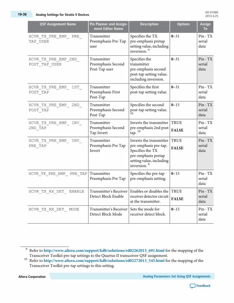
AssignTo
OptionsDescriptionPin Planner and Assign-ment Editor Name
QSF Assignment Name
Pin - TXserialdata
0–31Specifies the TXpre-emphasis pretapsetting value, includinginversion. 9
TransmitterPreemphasis Pre-Tapuser
XCVR_TX_PRE_EMP_ PRE_TAP_USER
Pin - TXserialdata
0–31Specifies thetransmitterpre-emphasis secondpost-tap setting value,including inversion.
TransmitterPreemphasis SecondPost-Tap user
XCVR_TX_PRE_EMP_2ND_POST_TAP_USER
Pin - TXserialdata
0–31Specifies the firstpost-tap setting value.
TransmitterPreemphasis FirstPost-Tap
XCVR_TX_PRE_EMP_ 1ST_POST_TAP
Pin - TXserialdata
0–15Specifies the secondpost-tap setting value.10
TransmitterPreemphasis SecondPost-Tap
XCVR_TX_PRE_EMP_ 2ND_POST_TAP
Pin - TXserialdata
TRUE
FALSE
Inverts the transmitterpre-emphasis 2nd posttap. 10
TransmitterPreemphasis SecondTap Invert
XCVR_TX_PRE_EMP_ INV_2ND_TAP
Pin - TXserialdata
TRUE
FALSE
Inverts the transmitterpre-emphasis pre-tap.Specifies the TXpre-emphasis pretapsetting value, includinginversion. 9
TransmitterPreemphasis Pre TapInvert
XCVR_TX_PRE_EMP_ INV_PRE_TAP
Pin - TXserialdata
0–15Specifies the pre-tappre-emphasis setting.
TransmitterPreemphasis Pre Tap
XCVR_TX_PRE_EMP_ PRE_TAP
Pin - TXserialdata
TRUE
FALSE
Enables or disables thereceiver detector circuitat the transmitter.
Transmitter's ReceiverDetect Block Enable
XCVR_TX_RX_DET_ ENABLE
Pin - TXserialdata
0–15Sets the mode forreceiver detect block.
Transmitter's ReceiverDetect Block Mode
XCVR_TX_RX_DET_ MODE
9 Refer to http://www.altera.com/support/kdb/solutions/rd02262013_691.html for the mapping of theTransceiver Toolkit pre-tap settings to the Quartus II transceiver QSF assignment.
10 Refer to http://www.altera.com/support/kdb/solutions/rd02272013_545.html for the mapping of theTransceiver Toolkit pre-tap settings to this setting.
Analog Parameters Set Using QSF AssignmentsAltera Corporation
Feedback
UG-01080Analog Settings for Stratix V Devices19-36 2013.4.25
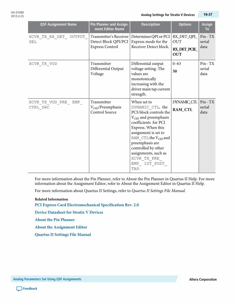
AssignTo
OptionsDescriptionPin Planner and Assign-ment Editor Name
QSF Assignment Name
Pin - TXserialdata
RX_DET_QPI_OUT
RX_DET_PCIE_OUT
DeterminesQPI or PCIExpress mode for theReceiver Detect block.
Transmitter's ReceiverDetect Block QPI/PCIExpress Control
XCVR_TX_RX_DET_ OUTPUT_SEL
Pin - TXserialdata
0–63
50
Differential outputvoltage setting. Thevalues aremonotonicallyincreasing with thedrivermain tap currentstrength.
TransmitterDifferential OutputVoltage
XCVR_TX_VOD
Pin - TXserialdata
DYNAMIC_CTL
RAM_CTL
When set toDYNAMIC_CTL, thePCS block controls theVOD and preemphasiscoefficients for PCIExpress. When thisassignment is set toRAM_CTL theVOD andpreemphasis arecontrolled by otherassignments, such asXCVR_TX_PRE_EMP_ 1ST_POST_TAP.
TransmitterVOD/PreemphasisControl Source
XCVR_TX_VOD_PRE_ EMP_CTRL_SRC
For more information about the Pin Planner, refer to About the Pin Planner in Quartus II Help. For moreinformation about the Assignment Editor, refer to About the Assignment Editor in Quartus II Help.
For more information about Quartus II Settings, refer to Quartus II Settings File Manual.
Related InformationPCI Express Card Electromechanical Specification Rev. 2.0
Device Datasheet for Stratix V Devices
About the Pin Planner
About the Assignment Editor
Quartus II Settings File Manual
Altera CorporationAnalog Parameters Set Using QSF Assignments
Feedback
19-37Analog Settings for Stratix V DevicesUG-010802013.4.25

20Migrating fromStratix IV to Stratix V DevicesOverview
2013.4.25UG-01080 Subscribe Feedback
Previously, Altera provided the ALTGX megafunction as a general purpose transceiver PHY solution. Thecurrent release of the Quartus II software includes protocol-specific PHY IP cores that simplify theparameterization process.
The design of these protocol-specific transceiver PHYs is modular and uses standard interfaces. AnAvalon-MM interface provides access to control and status registers that record the status of the PCS andPMA modules. Consequently, you no longer must include signals in the top level of your transceiver PHYto determine the status of the serial RX and TX interfaces. Using standard interfaces to access thisdevice-dependent information should ease future migrations to other device families and reduce the overalldesign complexity. However, to facilitate debugging, you may still choose to include some device-dependentsignals in the top level of your design during the initial simulations or even permanently. All protocol-specificPHY IP in Stratix V devices also include embedded controls for post-reset initialization which are availablethrough the Avalon-MM interface.
For Stratix IV devices, the location of the transceiver dynamic reconfiguration logic is design dependent. Ingeneral, reconfiguration logic is integrated with the transceiver channels for simple configurations and isseparately instantiated for more complex designs that use a large number of channels or instantiate morethan one protocol in a single transceiver quad. For Stratix V devices, transceiver dynamic reconfigurationis always performed using the separately instantiated Transceiver Reconfiguration Controller.
Control of loopback modes is also different in Stratix IV and Stratix V devices. For Stratix IV devices, youmust select loopback options in the using the MegaWizard Plug-In Manager. For Stratix V devices, youcontrol loopback modes through Avalon-MM registers.
Table 20-1: Controlling Loopback Modes in Stratix IV and Stratix V Devices
Stratix VStratix IVLoopback Mode
Use the Avalon-MM PHYmanagement interface to set theappropriate bit in the phy_serial_loopback register(0x061).
On the Loopback tab of the ALTGXMegaWizard Plug-In Manager, Instantiatethe rx_seriallpbken signal byselecting the Serial loopback option. Drivethis signal to 1 to put the transceiver in serialloopback mode.
Serial loopback
ISO9001:2008Registered
© 2013 Altera Corporation. All rights reserved. ALTERA, ARRIA, CYCLONE, HARDCOPY, MAX, MEGACORE, NIOS, QUARTUS and STRATIXwords and logos are trademarks of Altera Corporation and registered in the U.S. Patent and Trademark Office and in other countries. All other wordsand logos identified as trademarks or service marks are the property of their respective holders as described at www.altera.com/common/legal.html.Altera warrants performance of its semiconductor products to current specifications in accordance with Altera's standard warranty, but reserves theright to make changes to any products and services at any time without notice. Altera assumes no responsibility or liability arising out of the applicationor use of any information, product, or service described herein except as expressly agreed to in writing by Altera. Altera customers are advised toobtain the latest version of device specifications before relying on any published information and before placing orders for products or services.
www.altera.com
101 Innovation Drive, San Jose, CA 95134

Stratix VStratix IVLoopback Mode
Update the appropriate bits of theTransceiver ReconfigurationControllertx_rx_word_offsetregister to enable the pre- orpost-CDR reverse serial loopbackmode. Refer to PMA AnalogRegisters for more information.
On the Loopback tab of the ALTGXMegaWizard Plug-InManager, select eitherpre-CDR or post-CDR loopback andregenerate the ALTGX IP core.
Reverse serial loopback(pre- and post-CDR)
Related InformationTransceiver Reconfiguration Controller PMA Analog Control Registers on page 16-13
Differences in Dynamic Reconfiguration for Stratix IV and Stratix VTransceivers
Dynamic reconfiguration interface is completely new in StratixV devices. You cannot automaticallymigratea dynamic reconfiguration solution from Stratix IV to Stratix V devices.
Stratix V devices that include transceivers must use the Altera Transceiver Reconfiguration Controller thatcontains the offset cancellation logic to compensate for variations due to PVT. Initially, each transceiverchannel and eachTXPLLhas its ownparallel, dynamic reconfiguration bus, named reconfig_from_xcvr[45:0]and reconfig_to_xcvr[69:0]. The reconfiguration bus includes Avalon-MMsignals to read andwrite registersandmemory and test bus signals.When you instantiate a transceiver PHY in a StratixV device, the transceiverPHY IP core provides informational messages specifying the number of required reconfiguration interfacesin the message pane.
Example 20-1: Informational Messages for the Transceiver Reconfiguration Interface
PHY IP will require 5 reconfiguration interfaces for connectionto the external reconfiguration controller.
Reconfiguration interface offsets 0-3 are connected to thetransceiver channels.
Reconfiguration interface offset 4 is connected to the transmitPLL.
Although you must initially create a separate reconfiguration interface for each channel and TX PLL in yourdesign, when theQuartus II software compiles your design, it reduces the number of reconfiguration interfacesby merging reconfigurations interfaces. The synthesized design typically includes a reconfiguration interfacefor three channels. Allowing the Quartus II software to merge reconfiguration interfaces gives the Fittermore flexibility in placing transceiver channels.
Migrating from Stratix IV to Stratix V Devices OverviewAltera Corporation
Feedback
UG-01080Differences in Dynamic Reconfiguration for Stratix IV and Stratix V Transceivers20-2 2013.4.25

Stratix IV devices that include transceiversmust use theALTGX_RECONFIG IPCore to implement dynamicreconfiguration. The ALTGX_RECONFIG IP Core always includes the following two serial buses:
• reconfig_from[<n>16:0]— this bus connects to all the channels in a single quad. <n> is thenumber of quads connected to the ALTGX_RECONFIG IP Core.
• reconfig_togxb[3:0]—this single bus connects to all transceiver channels.
If you select additional functionality in the MegaWizard Plug-In Manager for the ALTGX_RECONFIG IPCore, the IP core adds signals to support that functionality. For more information about theALTGX_RECONFIG IP Core, refer to ALTGX_RECONFIGMegafunction User Guide for Stratix IV Devicesin volume 3 of the Stratix IV Device Handbook.
Related InformationALTGX_RECONFIG Megafunction User Guide for Stratix IV Devices
Differences Between XAUI PHY Parameters for Stratix IV and Stratix V Devices
Table 20-2: Comparison of ALTGX Megafunction and XAUI PHY Parameters
CommentsXAUI PHY Parameter NameALTGX Parameter Name (DefaultValue)
In Stratix V devices, this parameteris locked to 1 (for 4 channels). Youcannot change it in the currentrelease.
Number of XAUI interfacesNumber of channels
Use assignment editor tomake theseassignment
Not available as parameters in theMegaWizard Plug-In Managerinterface
Train receiver clock and datarecover (CDR) frompll_inclk (On)
TX PLL bandwidth mode (Auto)
RX CDR bandwidth mode (Auto)
Altera CorporationMigrating from Stratix IV to Stratix V Devices Overview
Feedback
20-3Differences Between XAUI PHY Parameters for Stratix IV and Stratix V DevicesUG-010802013.4.25
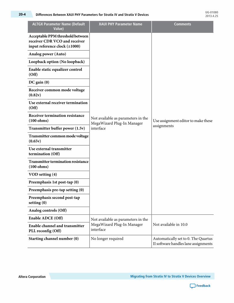
CommentsXAUI PHY Parameter NameALTGX Parameter Name (DefaultValue)
Use assignment editor tomake theseassignments
Not available as parameters in theMegaWizard Plug-In Managerinterface
AcceptablePPMthresholdbetweenreceiver CDR VCO and receiverinput reference clock (±1000)
Analog power (Auto)
Loopback option (No loopback)
Enable static equalizer control(Off)
DC gain (0)
Receiver common mode voltage(0.82v)
Use external receiver termination(Off)
Receiver termination resistance(100 ohms)
Transmitter buffer power (1.5v)
Transmitter commonmodevoltage(0.65v)
Use external transmittertermination (Off)
Transmitter termination resistance(100 ohms)
VOD setting (4)
Preemphasis 1st post-tap (0)
Preemphasis pre-tap setting (0)
Preemphasis second post-tapsetting (0)
Analog controls (Off)
Not available in 10.0Not available as parameters in theMegaWizard Plug-In Managerinterface
Enable ADCE (Off)
Enable channel and transmitterPLL reconfig (Off)
Automatically set to 0. The QuartusII software handles lane assignments
No longer requiredStarting channel number (0)
Migrating from Stratix IV to Stratix V Devices OverviewAltera Corporation
Feedback
UG-01080Differences Between XAUI PHY Parameters for Stratix IV and Stratix V Devices20-4 2013.4.25

CommentsXAUI PHY Parameter NameALTGX Parameter Name (DefaultValue)
Use assignment editorNot available as parameters in theMegaWizard Plug-In Managerinterface
Enable run length violationchecking with run length of (40)
Enable transmitter bit reversal(Off)
Word alignment pattern length(10)
Differences Between XAUI PHY Ports in Stratix IV and Stratix V DevicesThis section lists the differences between the top-level signals in Stratix IV GX and Stratix V GX/GS devices.
Table 20-3: Correspondences between XAUI PHY Stratix IV GX and Stratix V Device Signals
Stratix V DevicesStratix IV GX Devices11
WidthSignal NameWidthSignal Name
Reference Clocks and Resets
1refclk1pll_inclk
—Not available[<n> -1:0]rx_cruclk
1xgmii_rx_clk1coreclkout
—Not available[<n> -1:0]rx_coreclk
1xgmii_tx_clk[<n> -1:0]tx_coreclk
1rx_pma_ready—Not available
1tx_pma_ready—Not available
Data Ports
[3:0]xaui_rx_serial[<n> -1:0]rx_datain
[63:0]xgmii_tx_dc[16<n> -1:0]tx_datain
[63:0]xgmii_rx_dc[16<n> -1:0]rx_dataout
[3:0]xaui_tx_serial[<n> -1:0]tx_dataout
Optional TX and RX Status Ports
—Not available, however you canaccess them through theAvalon-MM PHY managementinterface.
[<n>/4 -1:0]gxb_powerdown
11 <n> = the number of lanes. <d> = the total deserialization factor from the pin to the FPGA fabric.
Altera CorporationMigrating from Stratix IV to Stratix V Devices Overview
Feedback
20-5Differences Between XAUI PHY Ports in Stratix IV and Stratix V DevicesUG-010802013.4.25

Stratix V DevicesStratix IV GX Devices11
WidthSignal NameWidthSignal Name
—Not available[<n> -1:0]pll_locked
—Not available[<n> -1:0]rx_locktorefclk
—Not available[<n> -1:0]rx_locktodata
—Not available[<n>/4 -1:0]rx_pll_locked
—Not available[<n>/4 -1:0]rx_freqlocked
—Not available[<n>/4 -1:0]rx_phase_comp_fifo_error
—Not available[<n>/4 -1:0]tx_phase_comp_fifo_error
—Not available—cal_blk_powerdown
[<n> *2 -1:0]rx_syncstatus[2<n> -1:0]rx_syncstatus
—Not available[2<n> -1:0]rx_patterndetect
—Not available[2<n> -1:0]rx_invpolarity
—Not available[2<n> -1:0]rx_ctrldetect
[<n> *2 -1:0]rx_errdetect[2<n> -1:0]rx_errdetect
[<n> *2 -1:0]rx_disperr[2<n> -1:0]rx_disperr
—Not available[2<n> -1:0]tx_invpolarity
—Not available[2<n> -1:0]rx_runningdisp
—Not available[2<n> -1:0]rx_rmfifofull
—Not available[2<n> -1:0]rx_rmfifoempty
—Not available[2<n> -1:0]rx_rmfifodatainserted
—Not available[2<n> -1:0]rx_rmfifodatadeleted
Transceiver Reconfiguration
—These signals are included in thereconfig_to_xcvr bus.
1cal_blk_clk
—1reconfig_clk
Variablereconfig_to_xcvr[3:0]reconfig_togxb
Variablereconfig_from_xcvr[16:0]reconfig_fromgxb
Avalon MM Management Interface
11 <n> = the number of lanes. <d> = the total deserialization factor from the pin to the FPGA fabric.
Migrating from Stratix IV to Stratix V Devices OverviewAltera Corporation
Feedback
UG-01080Differences Between XAUI PHY Ports in Stratix IV and Stratix V Devices20-6 2013.4.25
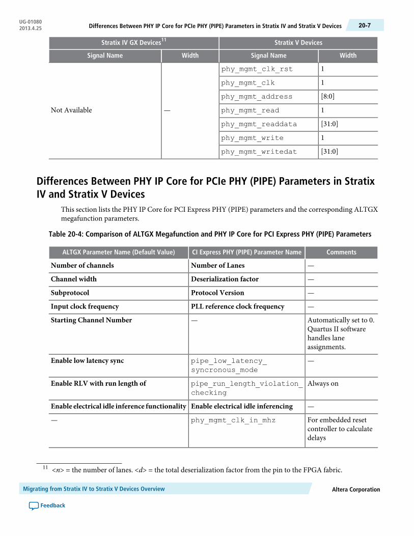
Stratix V DevicesStratix IV GX Devices11
WidthSignal NameWidthSignal Name
1phy_mgmt_clk_rst
—Not Available
1phy_mgmt_clk
[8:0]phy_mgmt_address
1phy_mgmt_read
[31:0]phy_mgmt_readdata
1phy_mgmt_write
[31:0]phy_mgmt_writedat
Differences Between PHY IP Core for PCIe PHY (PIPE) Parameters in StratixIV and Stratix V Devices
This section lists the PHY IP Core for PCI Express PHY (PIPE) parameters and the corresponding ALTGXmegafunction parameters.
Table 20-4: Comparison of ALTGX Megafunction and PHY IP Core for PCI Express PHY (PIPE) Parameters
CommentsCI Express PHY (PIPE) Parameter NameALTGX Parameter Name (Default Value)
—Number of LanesNumber of channels
—Deserialization factorChannel width
—Protocol VersionSubprotocol
—PLL reference clock frequencyInput clock frequency
Automatically set to 0.Quartus II softwarehandles laneassignments.
—Starting Channel Number
—pipe_low_latency_syncronous_mode
Enable low latency sync
Always onpipe_run_length_violation_checking
Enable RLV with run length of
—Enable electrical idle inferencingEnable electrical idle inference functionality
For embedded resetcontroller to calculatedelays
phy_mgmt_clk_in_mhz—
11 <n> = the number of lanes. <d> = the total deserialization factor from the pin to the FPGA fabric.
Altera CorporationMigrating from Stratix IV to Stratix V Devices Overview
Feedback
20-7Differences Between PHY IP Core for PCIe PHY (PIPE) Parameters in Stratix IV and Stratix V DevicesUG-010802013.4.25

CommentsCI Express PHY (PIPE) Parameter NameALTGX Parameter Name (Default Value)
Use assignment editorto make theseassignments
Not available inMegaWizard Interface
Train receiver CDR from pll_inclk (false)
TX PLL bandwidth mode (Auto)
RX CDR bandwidth mode (Auto)
Acceptable PPM threshold (±300)
Analog Power(VCCA_L/R) (Auto)
Reverse loopback option (No loopback)
Enable static equalizer control (false)
DC gain (1)
RX Vcm (0.82)
Force signal detection (Off)
Signal Detect threshold (4)
Use external receiver termination (Off)
RX term (100)
Transmitter buffer power(VCCH) (1.5)
TX Vcm (0.65)
Use external transmitter termination (Off)
TX Rterm (100)
VCO control setting (5)
Use assignment editorto make theseassignments
Not available inMegaWizard Interface
Pre-emphasis 1st post tap (18)
Pre-tap (0)
2nd post tap (0)
DPRIO - VOD, Pre-em, Eq and EyeQ (Off)
DPRIO-Channel andTXPLLReconfig (Off)
Differences Between PHY IP Core for PCIe PHY (PIPE) Ports for Stratix IV andStratix V Devices
This section lists the differences between the top-level signals in Stratix IV GX and Stratix V GX/GS devices.PIPE standard ports remain, but are now prefixed with pipe_. Clocking options are simplified to match thePIPE 2.0 specification.
Migrating from Stratix IV to Stratix V Devices OverviewAltera Corporation
Feedback
UG-01080Differences Between PHY IP Core for PCIe PHY (PIPE) Ports for Stratix IV and Stratix V Devices20-8 2013.4.25

Table 20-5: PCIe PHY (PIPE) Correspondence between Stratix IV GX Device and Stratix V Device Signals
WidthStratix V GX Device Signal NameStratix IV GX Device Signal Name12
Reference Clocks and Resets
1pll_ref_clkpll_inclk
[<n> -1:0]Not availablerx_cruclk
[<n> -1:0]Not availabletx_coreclk
[<n> -1:0]Not availablerx_coreclk
1pipe_pclktx_clkout/coreclkout
1These signals are now available as control andstatus registers. Refer to the "Avalon-MMPHYManagement Interface and PCI Express PHY(PIPE) IP Core Registers".
pll_powerdown
1cal_blk_powerdown
1tx_ready (reset control status)Not available
1rx_ready (reset curl status)Not available
PIPE interface Ports
[<n><d>-1:0]pipe_txdatatx_datain
[(<d>/8)*<n>-1:0]pipe_txdataktx_ctrlenable
[<n> -1:0]pipe_txdetectrx_loopbacktx_detectrxloop
[<n> -1:0]pipe_txcompliancetx_forcedispcompliance
[<n> -1:0]pipe_txelecidletx_forceelecidle
[<n> -1:0]pipe_txswingtxswing
[<n> -1:0]pipe_txdeemphtx_pipedeemph[0]
[3<n>-1:0]pipe_txmargintx_pipemargin[2:0]
[<n>-1:0]pipe_rate[1:0]rateswitch[0]
[2<n>-1:0]pipe_powerdownpowerdn
[3<n>-1:0]pipe_eidleinferselrx_elecidleinfersel
[<n>-*<d>-1:0]pipe_rxdatarx_dataout
[(<d>/8)*<n>-1:0]pipe_rxdatakrx_ctrldetect
[<n>-1:0]pipe_rxvalidpipedatavalid
[<n>-1:0]pipe_rxpolaritypipe8b10binvpolarity
[<n>-1:0]pipe_rxelecidlepipeelecidle
12 <n> = the number of lanes. <d> = the total deserialization factor from the pin to the FPGA fabric.
Altera CorporationMigrating from Stratix IV to Stratix V Devices Overview
Feedback
20-9Differences Between PHY IP Core for PCIe PHY (PIPE) Ports for Stratix IV and Stratix V DevicesUG-010802013.4.25
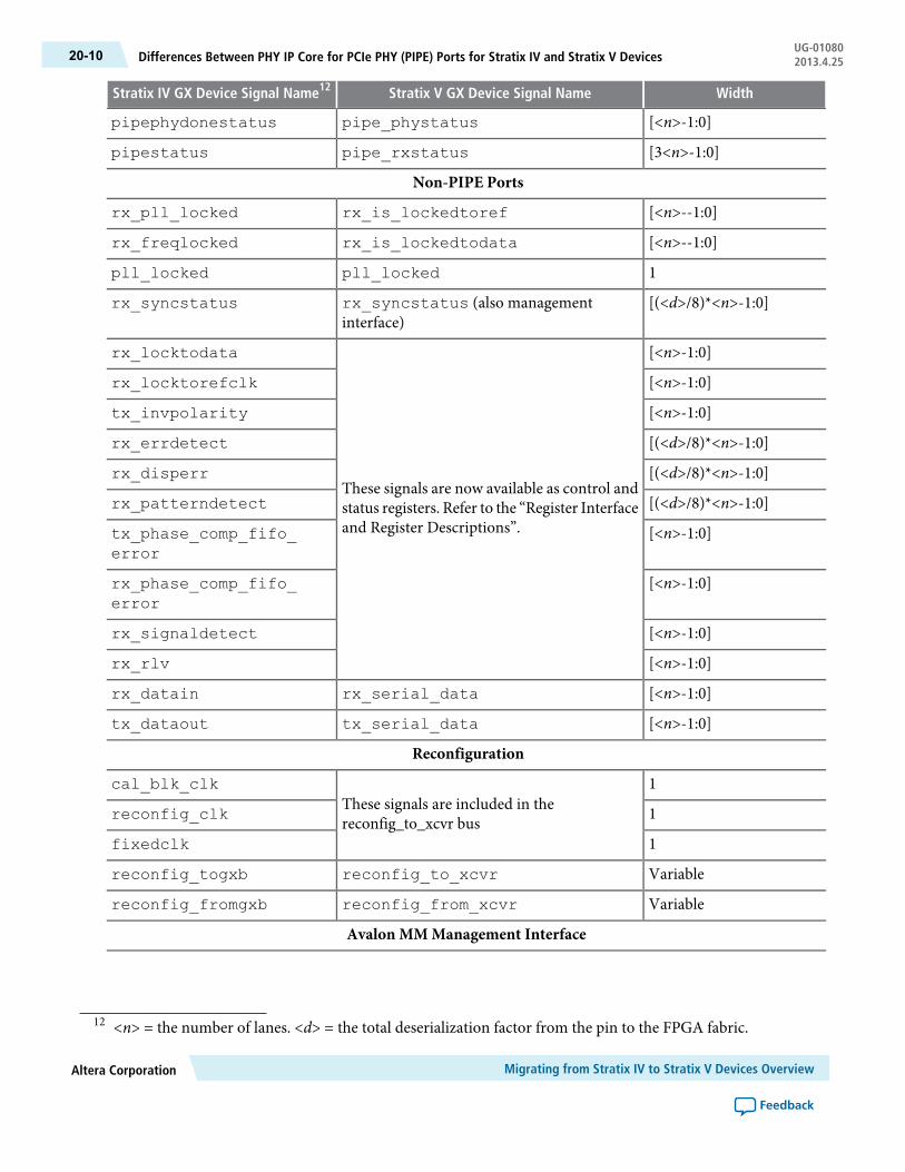
WidthStratix V GX Device Signal NameStratix IV GX Device Signal Name12
[<n>-1:0]pipe_phystatuspipephydonestatus
[3<n>-1:0]pipe_rxstatuspipestatus
Non-PIPE Ports
[<n>--1:0]rx_is_lockedtorefrx_pll_locked
[<n>--1:0]rx_is_lockedtodatarx_freqlocked
1pll_lockedpll_locked
[(<d>/8)*<n>-1:0]rx_syncstatus (also managementinterface)
rx_syncstatus
[<n>-1:0]
These signals are now available as control andstatus registers. Refer to the “Register Interfaceand Register Descriptions”.
rx_locktodata
[<n>-1:0]rx_locktorefclk
[<n>-1:0]tx_invpolarity
[(<d>/8)*<n>-1:0]rx_errdetect
[(<d>/8)*<n>-1:0]rx_disperr
[(<d>/8)*<n>-1:0]rx_patterndetect
[<n>-1:0]tx_phase_comp_fifo_error
[<n>-1:0]rx_phase_comp_fifo_error
[<n>-1:0]rx_signaldetect
[<n>-1:0]rx_rlv
[<n>-1:0]rx_serial_datarx_datain
[<n>-1:0]tx_serial_datatx_dataout
Reconfiguration
1These signals are included in thereconfig_to_xcvr bus
cal_blk_clk
1reconfig_clk
1fixedclk
Variablereconfig_to_xcvrreconfig_togxb
Variablereconfig_from_xcvrreconfig_fromgxb
Avalon MM Management Interface
12 <n> = the number of lanes. <d> = the total deserialization factor from the pin to the FPGA fabric.
Migrating from Stratix IV to Stratix V Devices OverviewAltera Corporation
Feedback
UG-01080Differences Between PHY IP Core for PCIe PHY (PIPE) Ports for Stratix IV and Stratix V Devices20-10 2013.4.25
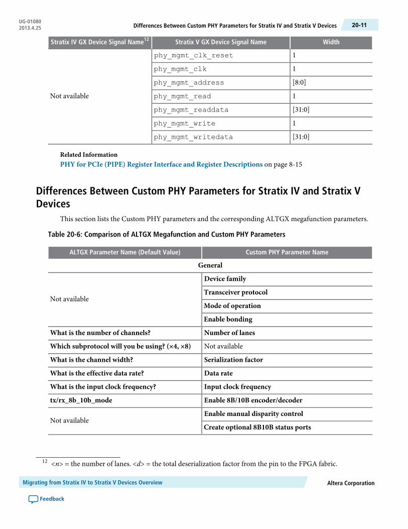
WidthStratix V GX Device Signal NameStratix IV GX Device Signal Name12
1phy_mgmt_clk_reset
Not available
1phy_mgmt_clk
[8:0]phy_mgmt_address
1phy_mgmt_read
[31:0]phy_mgmt_readdata
1phy_mgmt_write
[31:0]phy_mgmt_writedata
Related InformationPHY for PCIe (PIPE) Register Interface and Register Descriptions on page 8-15
Differences Between Custom PHY Parameters for Stratix IV and Stratix VDevices
This section lists the Custom PHY parameters and the corresponding ALTGX megafunction parameters.
Table 20-6: Comparison of ALTGX Megafunction and Custom PHY Parameters
Custom PHY Parameter NameALTGX Parameter Name (Default Value)
General
Device family
Not availableTransceiver protocol
Mode of operation
Enable bonding
Number of lanesWhat is the number of channels?
Not availableWhich subprotocol will you be using? (×4, ×8)
Serialization factorWhat is the channel width?
Data rateWhat is the effective data rate?
Input clock frequencyWhat is the input clock frequency?
Enable 8B/10B encoder/decodertx/rx_8b_10b_mode
Enable manual disparity controlNot available
Create optional 8B10B status ports
12 <n> = the number of lanes. <d> = the total deserialization factor from the pin to the FPGA fabric.
Altera CorporationMigrating from Stratix IV to Stratix V Devices Overview
Feedback
20-11Differences Between Custom PHY Parameters for Stratix IV and Stratix V DevicesUG-010802013.4.25

Custom PHY Parameter NameALTGX Parameter Name (Default Value)
Deserializer block width: 13
Auto
Single
Double
What is the deserializer block width?
Single
Double
Additional Options
Enable TX Bitslip
Not available
Create rx_coreclkin port
Create tx_coreclkin port
Create rx_recovered_clk port
Create optional ports
Avalon data interfaces
Force manual reset control
Word AlignerProtocol Settings-Word Aligner
Word alignment modeUse manual word alignment mode
Use manual bitslipping mode
Use the built-in 'synchronization state machine'
Run lengthEnable run length violation checking with a runlength of
Word alignment patternWhat is the word alignment pattern
Word aligner pattern lengthWhat is the word alignment pattern length
Rate MatchProtocol Settings-Rate match/Byte order
Rate match insertion/deletion +ve disparity patternWhat is the 20-bit rate match pattern1
(usually used for +ve disparity pattern)
Rate match insertion/deletion -ve disparity patternWhat is the 20-bit rate match pattern1
(usually used for -ve disparity pattern)
Byte OrderProtocol Settings—Rate match/Byte order
Byte ordering patternWhat is the byte ordering pattern
13 This parameter is on the Datapath tab.
Migrating from Stratix IV to Stratix V Devices OverviewAltera Corporation
Feedback
UG-01080Differences Between Custom PHY Parameters for Stratix IV and Stratix V Devices20-12 2013.4.25

Differences Between Custom PHY Ports in Stratix IV and Stratix V DevicesThis section lists the differences between the top-level signals in Stratix IV GX and Stratix V GX/GS devices.
Table 20-7: Custom PHY Correspondences between Stratix IV GX Device and Stratix V Device Signals
WidthCustom PHYALTGX14
Avalon-MM Management Interface
1phy_mgmt_clk_reset
Not available
1phy_mgmt_clk
8phy_mgmt_address
1phy_mgmt_read
32phy_mgmt_readdata
1phy_mgmt_write
32phy_mgmt_writedata
Clocks
—These signals are included in thereconfig_to_xcvr bus
cal_blk_clk
—reconfig_clk
[<p>-1:0]pll_ref_clkpll_inclk
—rx_coreclkinrx_coreclk
—tx_coreclkintx_coreclk
Avalon-ST TX Interface
[<d><n>-1:0]tx_parallel_datatx_datain
[<d><n>-1:0]tx_dataktx_ctrlenable
[<d><n>-1:0]rx_datakrx_ctrldetect
Avalon-ST RX Interface
[<d><n>-1:0]rx_parallel_datarx_dataout
[<d/8><n>-1:0]rx_runningdisprx_runningdisp
[<n>-1:0]rx_enabyteordrx_enabyteord
High Speed Serial I/O
[<n>-1:0]rx_serial_datarx_datain
[<n>-1:0]tx_serial_datatx_dataout
14 <n> = the number of lanes. <d> = the total deserialization factor from the pin to the FPGA fabric.
Altera CorporationMigrating from Stratix IV to Stratix V Devices Overview
Feedback
20-13Differences Between Custom PHY Ports in Stratix IV and Stratix V DevicesUG-010802013.4.25

WidthCustom PHYALTGX14
[<n>-1:0]rx_is_lockedtodatarx_freqlocked
Transceiver Control and Status Signals
—phy_mgmt_clk_resetgxb_powerdown
——rx_dataoutfull
——tx_dataoutfull
—There are both pll_locked andrx_pll_clocked in Stratix IV. Stratix Vonly has pll_locked.
rx_pll_locked
—
These signals are now available ascontrol and status registers. Refer toRegister Descriptions.
rx_clkout
—rx_phase_comp_fifo_error
—rx_seriallpbken
—tx_phase_comp_fifo_error
—tx_invpolarity
Transceiver Reconfiguration
Variablereconfig_to_xcvrreconfig_togxb[3:0]
Variablereconfig_from_xcvrreconfig_fromgxb[16:0]
Related InformationRegister Interface and Register Descriptions on page 9-23
14 <n> = the number of lanes. <d> = the total deserialization factor from the pin to the FPGA fabric.
Migrating from Stratix IV to Stratix V Devices OverviewAltera Corporation
Feedback
UG-01080Differences Between Custom PHY Ports in Stratix IV and Stratix V Devices20-14 2013.4.25

21Additional Information for the TransceiverPHY IP Core
2013.4.25UG-01080 Subscribe Feedback
This section provides the revision history for the chapters in this user guide.Changes MadeDocument
VersionDate
Introduction
Update to introduction. Renamed heading "Additional Transceiver PHYs"to "Non-Protocol-Specific Transceiver PHYs."
2.1April 2013
Getting Started
No changes from previous release.2.1April 2013
10GBASE-R
No changes from previous release.2.1April 2013
10GBASE-KR
No changes from previous release.2.1April 2013
1Gbe/10GbE
No changes from previous release.2.1April 2013
XAUI
Fixed minor topographical error in heading.2.1April 2013
Interlaken
No changes from previous release.2.1April 2013
PHY IP Core for PCI Express
No changes from previous release.2.1April 2013
Custom PHY
No changes from previous release.2.1April 2013
Low Latency PHY
No changes from previous release.2.1April 2013
Deterministic Latency PHY
ISO9001:2008Registered
© 2013 Altera Corporation. All rights reserved. ALTERA, ARRIA, CYCLONE, HARDCOPY, MAX, MEGACORE, NIOS, QUARTUS and STRATIXwords and logos are trademarks of Altera Corporation and registered in the U.S. Patent and Trademark Office and in other countries. All other wordsand logos identified as trademarks or service marks are the property of their respective holders as described at www.altera.com/common/legal.html.Altera warrants performance of its semiconductor products to current specifications in accordance with Altera's standard warranty, but reserves theright to make changes to any products and services at any time without notice. Altera assumes no responsibility or liability arising out of the applicationor use of any information, product, or service described herein except as expressly agreed to in writing by Altera. Altera customers are advised toobtain the latest version of device specifications before relying on any published information and before placing orders for products or services.
www.altera.com
101 Innovation Drive, San Jose, CA 95134

Changes MadeDocumentVersion
Date
No changes from previous release.2.1April 2013
Stratix V Native PHY
Removed Arria V GT sentence on first page.2.1April 2013
Arria V Native PHY
No changes from previous release.2.1April 2013
Arria V GZ Native PHY
Removed Arria V GT sentence on first page.2.1April 2013
Cyclone V Native PHY
No changes from previous release.2.1April 2013
Transceiver Reconfiguration Controller
Rename table 16-13 to DFE Registers. Fix typo in Reconfig Addr columnchanged 7’h11 to 7’h19. In Table 16-8, removed theDCDCalibration registersrow.
2.1April 2013
Transceiver Reset Controller
No changes from previous release.2.1April 2013
Transceiver Reset Controller
No changes from previous release.2.1April 2013
Transceiver PLL for Arria V, Arria V GZ, and Stratix V Devices
No changes from previous release.2.1April 2013
Analog Parameters Set Using QSF Assignment
Fix typo in the "Analog Settings for Arria V GZ Devices" table.2.1April 2013
Migrating from Stratix IV to Stratix V Devices
No changes from previous release.2.1April 2013
Changes MadeDocumentVersion
Date
Introduction
No changes from previous release.2.0March 2013
Getting Started
No changes from previous release.2.0March 2013
10GBASE-R
No changes from previous release.2.0March 2013
Additional Information for the Transceiver PHY IP CoreAltera Corporation
Feedback
UG-01080Additional Information for the Transceiver PHY IP Core21-2 2013.4.25
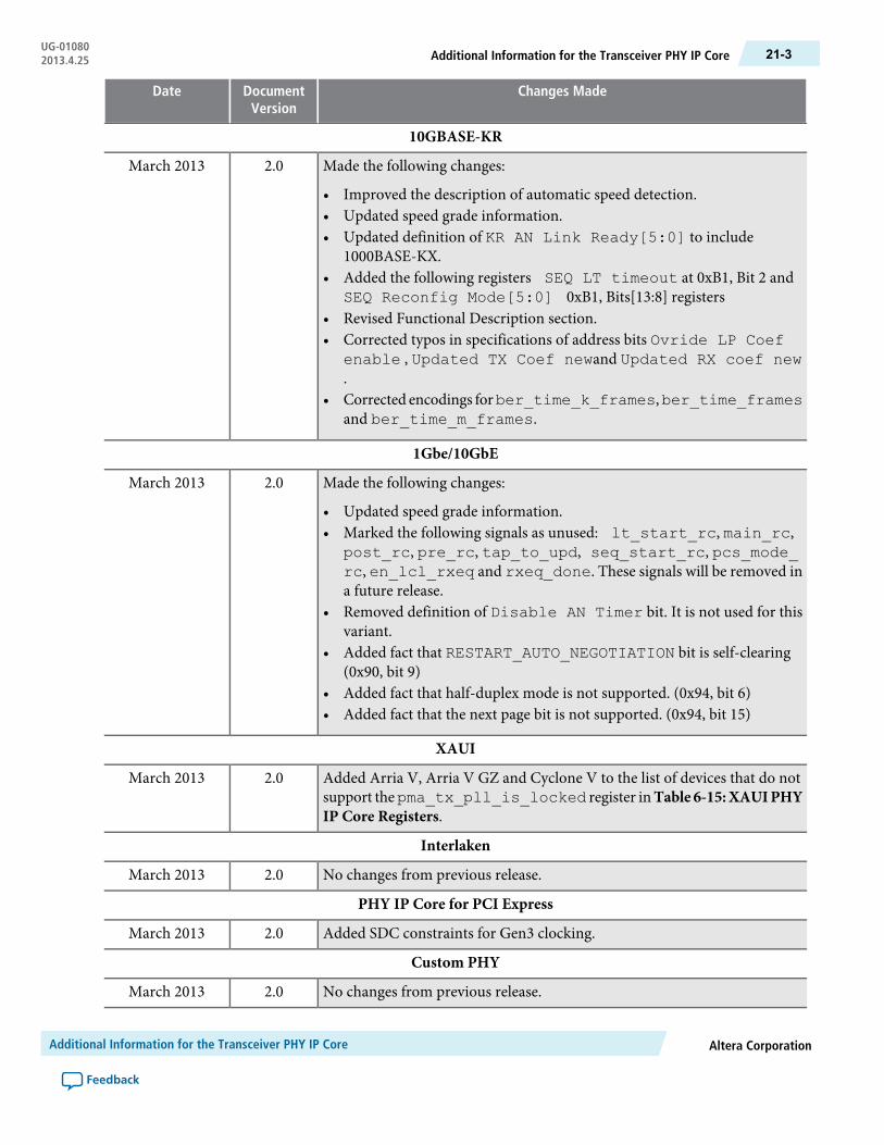
Changes MadeDocumentVersion
Date
10GBASE-KR
Made the following changes:
• Improved the description of automatic speed detection.• Updated speed grade information.• Updated definition of KR AN Link Ready[5:0] to include
1000BASE-KX.• Added the following registers SEQ LT timeout at 0xB1, Bit 2 and
SEQ Reconfig Mode[5:0] 0xB1, Bits[13:8] registers• Revised Functional Description section.• Corrected typos in specifications of address bits Ovride LP Coef
enable , Updated TX Coef newand Updated RX coef new.
• Corrected encodings forber_time_k_frames,ber_time_framesand ber_time_m_frames.
2.0March 2013
1Gbe/10GbE
Made the following changes:
• Updated speed grade information.• Marked the following signals as unused: lt_start_rc, main_rc,
post_rc, pre_rc, tap_to_upd, seq_start_rc, pcs_mode_rc, en_lcl_rxeq and rxeq_done. These signals will be removed ina future release.
• Removed definition of Disable AN Timer bit. It is not used for thisvariant.
• Added fact that RESTART_AUTO_NEGOTIATION bit is self-clearing(0x90, bit 9)
• Added fact that half-duplex mode is not supported. (0x94, bit 6)• Added fact that the next page bit is not supported. (0x94, bit 15)
2.0March 2013
XAUI
Added Arria V, Arria V GZ and Cyclone V to the list of devices that do notsupport thepma_tx_pll_is_locked register inTable 6-15:XAUIPHYIP Core Registers.
2.0March 2013
Interlaken
No changes from previous release.2.0March 2013
PHY IP Core for PCI Express
Added SDC constraints for Gen3 clocking.2.0March 2013
Custom PHY
No changes from previous release.2.0March 2013
Altera CorporationAdditional Information for the Transceiver PHY IP Core
Feedback
21-3Additional Information for the Transceiver PHY IP CoreUG-010802013.4.25

Changes MadeDocumentVersion
Date
Low Latency PHY
No changes from previous release.2.0March 2013
Deterministic Latency PHY
No changes from previous release.2.0March 2013
Stratix V Native PHY
Updated definition of User external TXPLL to include information on howto instantiate an external PLL.
2.0March 2013
Arria V Native PHY
Updated definition of User external TXPLL to include information on howto instantiate an external PLL.
2.0March 2013
Arria V GZ Native PHY
Updated definition of User external TXPLL to include information on howto instantiate an external PLL.
2.0March 2013
Cyclone V Native PHY
Updated definition of User external TXPLL to include information on howto instantiate an external PLL.
2.0March 2013
Transceiver Reconfiguration Controller
Additional Information for the Transceiver PHY IP CoreAltera Corporation
Feedback
UG-01080Additional Information for the Transceiver PHY IP Core21-4 2013.4.25

Changes MadeDocumentVersion
Date
Made the following changes:
• Updated definition ofTX PLL select at 0x4 in Table 16-21: PLLReconfiguration Offsets and Values.
• Changed Figure 16-5: MIF File Formatto match data in Table 16-26.• Changed Example 16-11 to read the busy bit after each command,
read_32 0x3a.• Added SDC timing constraints.• Changed RX Equalization Control0x11 in Table 16-10: PMA
Offsets and Values to RW. This change is available starting with QuartusII 12.1 SP1.
• Clarified encodings for RX equalization DC gain inTable16-10:PMA Offsets and Values.
• Clarified encodings for pre-emphasis pre-tap and pre-emphasis secondpost-tap in Table 16-10: PMA Offsets and Values.
• Clarified fact that you can only connect a single TransceiverReconfiguration Controller to a single transceiver PHY.
• Updated recommendations for use of DCD in Arria V and Cyclone Vdevices. You should use DCD if the data rate is greater than 4.9152 Gbpsor if there is dynamic TX PLL switching and the data rate is greater than4.9152 Gbps. Updated address map and illustration to include DCDfunction.
2.0March 2013
Transceiver Reset Controller
Added tx_ready and rx_ready to Figure 17-1.2.0March 2013
Transceiver PLL for Arria V, Arria V GZ, and Stratix V Devices
Initial Release.2.0March 2013
Analog Parameters Set Using QSF Assignment
Made the following changes.
• Changed choices for XCVR_RX_SD_ENABLE from TRUE/FALSE toOn/Off
• Corrected definitions of XCVR_IO_PIN_TERMINATION and XCVR_GT_IO_PIN_TERMINATION which were reversed.
• Added references to Knowledge Base Solution showing the mapping ofTransceiverToolkit settings toXCVR_TX_PRE_EMP_PRE_TAP,XCVR_TX_PRE_EMP_INV_PRE_TAP andXCVR_TX_PRE_EMP_PRE_TAP_USER for Arria V GZ and Stratix V devices.
• Added references to Knowledge Base Solution showing the mapping ofTransceiver Toolkit settings toXCVR_TX_PRE_EMP_2ND_POST_TAP,XCVR_TX_PRE_EMP_INV_2ND_TAP, and XCVR_TX_PRE_EMP_2ND_POST_TAP_USER for Arria V GZ and Stratix V devices.
2.0March 2013
Altera CorporationAdditional Information for the Transceiver PHY IP Core
Feedback
21-5Additional Information for the Transceiver PHY IP CoreUG-010802013.4.25

Changes MadeDocumentVersion
Date
Migrating from Stratix IV to Stratix V Devices
No changes from previous release.2.0March 2013
Changes MadeDocumentVersion
Date
Introduction and Getting Started
• Reformatted.1.9February 2013
10GBASE-R PHY
• Reformatted.• Corrected definition of the PLL type parameter. Altera recommends the
ATX PLL for data rates greater than 8 Gbps.
1.9February 2013
Backplane Ethernet 10GBASE-KR PHY
• Reformatted.• Removed description of PMA reset_ch_bitmask at 0x41 which is
not available. Added definition of digital and analog resets at 0x44, bits1-3.
• Removed definitions of trn_in_trigger andtrn_out_triggerbuses which are not used.
• Corrected direction of xgmii_rx_clk in pinout figure.
1.9February 2013
1G/10GbE PHY
• Reformatted.• Corrected definition of rx_data_ready. This signal is used and
indicates that the PCS is ready to receive data.• Removed description of PMA reset_ch_bitmask at 0x41 and
reset_control at 0x42 which are not available.• Removed definitions of trn_in_trigger andtrn_out_trigger
buses which are not used.
1.9February 2013
XAUI PHY
• Reformatted.1.9February 2013
Interlaken PHY
• Reformatted.• Improved definitions of rx_parallel_data<n>[68], rx_
dataout_bp<n> and typo in definition of tx_user_clkout.
1.9February 2013
PHY IP Core for PCI Express (PIPE)
• Reformatted.1.9February 2013
Additional Information for the Transceiver PHY IP CoreAltera Corporation
Feedback
UG-01080Additional Information for the Transceiver PHY IP Core21-6 2013.4.25

Changes MadeDocumentVersion
Date
Custom PHY
• Reformatted.1.9February 2013
Low Latency PHY
• Reformatted.1.9February 2013
Deterministic Latency PHY
• Reformatted.• Corrected headings in Table 11-4. The TX PMA Latency in UI and RX
PMA Latency in UI were previously reversed.• In Table 11-3, added explanation of a latency uncertainty of 0.5 cycles
when the byte serializer/deserializer is turned on. The location of thealignment pattern which can be in the upper or lower symbol.
1.9February 2013
Stratix V Native PHY
• Reformatted.• Added missing descriptions of Interlaken parameters to 10G RX FIFO
section.• Improved definition of pll_powerdown signal.
1.9February 2013
Arria V Native PHY
• Reformatted.• RemovedQPI signals fromFigure showingArriaVNative PHYCommon
Interfaces. These signals are not available for Arria V devices.• Removed SDC constraints for 10G signals which are not available for
Arria V.
1.9February 2013
Arria V GZ Native PHY
• Reformatted.• Improved definition of pll_powerdown signal.
1.9February 2013
Cyclone V Native PHY
• Reformatted.• Removed information about PMA direct mode. PMA direct mode is not
supported for Cyclone V devices.• Improved definition of pll_powerdown signal.
1.9February 2013
Transceiver Reconfiguration Controller
• Reformatted.• Expanded definition of mgmt_clk_clk to include constraints when CvP is
enabled and frequency range for Arria V GZ and Cyclone V devices.• Corrected address for channel 2 in register-based read examples.
1.9February 2013
Altera CorporationAdditional Information for the Transceiver PHY IP Core
Feedback
21-7Additional Information for the Transceiver PHY IP CoreUG-010802013.4.25

Changes MadeDocumentVersion
Date
Transceiver PHY Reset Controller
• Reformatted.• Improved definition of pll_powerdown and rx_manualsignals.
1.9February 2013
Analog Parameters Set Using QSF Assignments
• Reformatted.• Added the following settings to the Arria V and Cyclone V tables:XCVR_
RX_SD_ON, XCVR_RX_SD_OFF, XCVR_RX_SD_THRESHOLD,CDR_BANDWIDTH_PRESET, XCVR_RX_COMMON_MODE_VOLTAGE,XCVR_TX_COMMON_MODE_VOLTAGE, XCVR_TX_RX_DET_ENABLE, and XCVR_RX_DET_MODE.
1.9February 2013
Migrating from Stratix IV to Stratix V Devices
• Reformatted.1.9February 2013
Introduction
• Expanded discussion of the Arria V, Arria V GZ, Cyclone V, and StratixV Transceiver Native PHY IP Cores.
• Added Riviera-PRO Aldec simulation directory.
1.8November 2012
10GBASE-R PHY
• Added support for IEEE 1588 Precision Time Protocol.• Added Arria V GZ support.• Enabled RCLR_BER_COUNT (0x81, bit 3) and HI_BER (0x82, bit 1) for
Arria V GZ and Stratix V devices.• Moved Analog Options to a separate chapter.
1.8November 2012
10GBASE-KR PHY
• Initial release.1.8November 2012
1G/10 Gbps Ethernet PHY
• Initial release.1.8November 2012
XAUI PHY
• Added Arria V GZ support.• Moved Analog Options to a separate chapter.• Added constraint for tx_digitalreset when TX PCS uses bonded
clocks.
1.8November 2012
Interlaken PHY
Additional Information for the Transceiver PHY IP CoreAltera Corporation
Feedback
UG-01080Additional Information for the Transceiver PHY IP Core21-8 2013.4.25
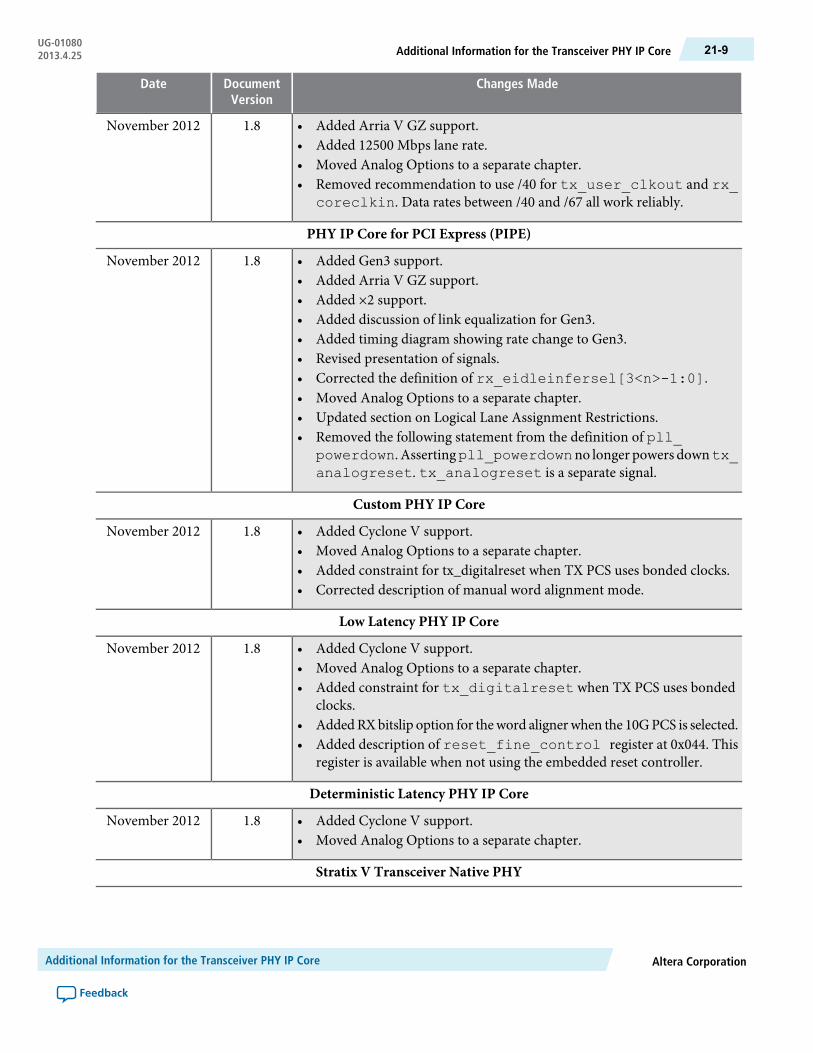
Changes MadeDocumentVersion
Date
• Added Arria V GZ support.• Added 12500 Mbps lane rate.• Moved Analog Options to a separate chapter.• Removed recommendation to use /40 for tx_user_clkout and rx_
coreclkin. Data rates between /40 and /67 all work reliably.
1.8November 2012
PHY IP Core for PCI Express (PIPE)
• Added Gen3 support.• Added Arria V GZ support.• Added ×2 support.• Added discussion of link equalization for Gen3.• Added timing diagram showing rate change to Gen3.• Revised presentation of signals.• Corrected the definition of rx_eidleinfersel[3<n>-1:0].• Moved Analog Options to a separate chapter.• Updated section on Logical Lane Assignment Restrictions.• Removed the following statement from the definition of pll_
powerdown. Assertingpll_powerdownno longer powers downtx_analogreset. tx_analogreset is a separate signal.
1.8November 2012
Custom PHY IP Core
• Added Cyclone V support.• Moved Analog Options to a separate chapter.• Added constraint for tx_digitalreset when TX PCS uses bonded clocks.• Corrected description of manual word alignment mode.
1.8November 2012
Low Latency PHY IP Core
• Added Cyclone V support.• Moved Analog Options to a separate chapter.• Added constraint for tx_digitalreset when TX PCS uses bonded
clocks.• AddedRXbitslip option for theword alignerwhen the 10GPCS is selected.• Added description of reset_fine_control register at 0x044. This
register is available when not using the embedded reset controller.
1.8November 2012
Deterministic Latency PHY IP Core
• Added Cyclone V support.• Moved Analog Options to a separate chapter.
1.8November 2012
Stratix V Transceiver Native PHY
Altera CorporationAdditional Information for the Transceiver PHY IP Core
Feedback
21-9Additional Information for the Transceiver PHY IP CoreUG-010802013.4.25

Changes MadeDocumentVersion
Date
• Added support for Standard and 10G datapaths.• Added QPI interface.• Moved Analog Options to a separate chapter.• Added constraint for tx_digitalreset when TX PCS uses bonded
clocks.
1.8November 2012
Arria V Transceiver Native PHY
• Added support for Standard datapath.• Added support for multiple PLLs.• Moved Analog Options to a separate chapter.• Added constraint for tx_digitalreset when TX PCS uses bonded
clocks.
1.8November 2012
Arria V GZ Transceiver Native PHY
• Initial release.1.8November 2012
Cyclone V Transceiver Native PHY
• Initial release.1.8November 2012
Reconfiguration Controller
• Added MIF addressing mode option. Byte and word (16 bits)addressing are available.
• Added ATX PLL reference clock switching and reconfiguration of ATXPLL settings, including counters.
• Added support for ATX PLL reconfiguration.• Added statement that if you are using the EyeQ monitor when DFE is
enabled, if you must use the EyeQ monitor with a 1D-eye.• Corrected definition of DFE_control bit at 0xa. This register is write
only.• Removed duty cycle calibration. This function is run automatically during
the power-on sequence.• Added DFE support including examples showing how to program this
function.• Added DCD for Arria V devices.• Updated data for writes in Streamer Mode 1 Reconfiguration.• Changed data value to write in step 7 of Streamer-Based Reconfiguration.• Changed data value to write to setup streaming in Reconfiguration of
Logical Channel 0 Using a MIF.
1.8November 2012
Transceiver PHY Reset Controller
Additional Information for the Transceiver PHY IP CoreAltera Corporation
Feedback
UG-01080Additional Information for the Transceiver PHY IP Core21-10 2013.4.25

Changes MadeDocumentVersion
Date
• Added Arria V GZ support.• Added SDC constraint for tx_digitalreset when TX PCS uses
bonded clocks.
1.8November 2012
Analog Parameters Set Using QSF Assignments
• Created separate chapter for analog parameters that were previously listedin the individual transceiver PHY chapters.
• Changed default value for XCVR_GT_RX_COMMON_MODE_VOLTAGEto 0.65V.
1.8November 2012
Introduction and Getting Started
• Added brief discussion of the Stratix V and Arria V Transceiver NativePHY IP Cores.
1.7June 2012
Getting Started
• No changes from the previous release.1.7June 2012
10GBASE-R PHY
• Added the following QSF settings to all transceiver PHY: XCVR_TX_PRE_EMP_PRE_TAP_USER,XCVR_TX_PRE_EMP_2ND_POST_TAP_USER, and 11 new settings for GT transceivers.
• Added Arria V device support.• Changed the default value for XCVR_REFCLK_PIN_TERMINATION
from DC_coupling_internal_100_Ohm to AC_coupling.• Changed references to Stratix IV GX to Stratix IV GT. This IP core only
supports Stratix IV GT devices.• Added optional pll_locked status signal for Arria V and Stratix V
devices. Added optional rx_coreclkin.• Added arrowsTransceiver ReconfigurationController IPCore connection
to block diagram.• Changed themaximum frequency ofphy_mgmt_clk to 150MHz if the
same clock is used for the Transceiver ReconfigurationController IPCore.• Added the following restriction in the dynamic reconfiguration section:
three channels share an Avalon-MM slave interface which must connectto the same Transceiver Reconfiguration Controller IP Core.
• Added example showing how to override the logical channel 0 channelassignment in Stratix V devices.
• Added table showing latency through PCS and PMA for Arria V andStratix V devices.
1.7June 2012
XAUI PHY
Altera CorporationAdditional Information for the Transceiver PHY IP Core
Feedback
21-11Additional Information for the Transceiver PHY IP CoreUG-010802013.4.25
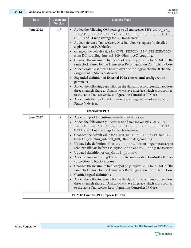
Changes MadeDocumentVersion
Date
• Added the following QSF settings to all transceiver PHY: XCVR_TX_PRE_EMP_PRE_TAP_USER,XCVR_TX_PRE_EMP_2ND_POST_TAP_USER, and 11 new settings for GT transceivers.
• Added reference Transceiver device handbook chapters for detailedexplanation of PCS blocks.
• Changed the default value for XCVR_REFCLK_PIN_TERMINATIONfrom DC_coupling_internal_100_Ohm to AC_coupling.
• Changed themaximum frequency ofphy_mgmt_clk to 150MHz if thesame clock is used for the Transceiver ReconfigurationController IPCore.
• Added example showing how to override the logical channel 0 channelassignment in Stratix V devices.
• Expanded definition of External PMA control and configurationparameter.
• Added the following restriction in the dynamic reconfiguration section:three channels share an Avalon-MM slave interface which must connectto the same Transceiver Reconfiguration Controller IP Core.
• Added note that cal_blk_powerdown register is not available forStratix V devices.
1.7June 2012
Interlaken PHY
• Added support for custom, user-defined, data rates.• Added the following QSF settings to all transceiver PHY: XCVR_TX_
PRE_EMP_PRE_TAP_USER,XCVR_TX_PRE_EMP_2ND_POST_TAP_USER, and 11 new settings for GT transceivers.
• Changed the default value for XCVR_REFCLK_PIN_TERMINATIONfrom DC_coupling_internal_100_Ohm to AC_coupling.
• Updated the definition of tx_sync_done. It is no longer necessary tosend pre-fill data before tx_sync_done and tx_ready are asserted.
• Updated definition of tx_datain_bp<n>.• Added arrows indicating Transceiver ReconfigurationController IP Core
connection to block diagram.• Changed themaximum frequency ofphy_mgmt_clk to 150MHz if the
same clock is used for the Transceiver ReconfigurationController IPCore.• Clarified signal definitions.• Added the following restriction in the dynamic reconfiguration section:
three channels share an Avalon-MM slave interface which must connectto the same Transceiver Reconfiguration Controller IP Core.
1.7June 2012
PHY IP Core for PCI Express (PIPE)
Additional Information for the Transceiver PHY IP CoreAltera Corporation
Feedback
UG-01080Additional Information for the Transceiver PHY IP Core21-12 2013.4.25
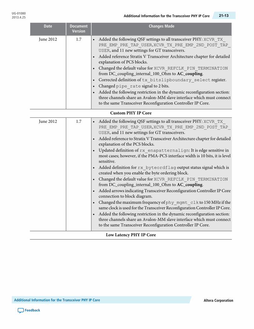
Changes MadeDocumentVersion
Date
• Added the following QSF settings to all transceiver PHY: XCVR_TX_PRE_EMP_PRE_TAP_USER,XCVR_TX_PRE_EMP_2ND_POST_TAP_USER, and 11 new settings for GT transceivers.
• Added reference Stratix V Transceiver Architecture chapter for detailedexplanation of PCS blocks.
• Changed the default value for XCVR_REFCLK_PIN_TERMINATIONfrom DC_coupling_internal_100_Ohm to AC_coupling.
• Corrected definition of tx_bitslipboundary_select register.• Changed pipe_rate signal to 2 bits.• Added the following restriction in the dynamic reconfiguration section:
three channels share an Avalon-MM slave interface which must connectto the same Transceiver Reconfiguration Controller IP Core.
1.7June 2012
Custom PHY IP Core
• Added the following QSF settings to all transceiver PHY: XCVR_TX_PRE_EMP_PRE_TAP_USER,XCVR_TX_PRE_EMP_2ND_POST_TAP_USER, and 11 new settings for GT transceivers.
• Added reference to Stratix VTransceiver Architecture chapter for detailedexplanation of the PCS blocks.
• Updated definition of rx_enapatternalign: It is edge sensitive inmost cases; however, if the PMA-PCS interface width is 10 bits, it is levelsensitive.
• Added definition for rx_byteordflag output status signal which iscreated when you enable the byte ordering block.
• Changed the default value for XCVR_REFCLK_PIN_TERMINATIONfrom DC_coupling_internal_100_Ohm to AC_coupling.
• Added arrows indicating Transceiver ReconfigurationController IP Coreconnection to block diagram.
• Changed themaximum frequency ofphy_mgmt_clk to 150MHz if thesame clock is used for the Transceiver ReconfigurationController IPCore.
• Added the following restriction in the dynamic reconfiguration section:three channels share an Avalon-MM slave interface which must connectto the same Transceiver Reconfiguration Controller IP Core.
1.7June 2012
Low Latency PHY IP Core
Altera CorporationAdditional Information for the Transceiver PHY IP Core
Feedback
21-13Additional Information for the Transceiver PHY IP CoreUG-010802013.4.25

Changes MadeDocumentVersion
Date
• Added the following QSF settings to all transceiver PHY: XCVR_TX_PRE_EMP_PRE_TAP_USER,XCVR_TX_PRE_EMP_2ND_POST_TAP_USER, and 11 new settings for GT transceivers.
• Changed the default value for XCVR_REFCLK_PIN_TERMINATIONfrom DC_coupling_internal_100_Ohm to AC_coupling.
• Added arrows indicating Transceiver ReconfigurationController IP Coreconnection to block diagram.
• Changed the maximum frequency of phy_mgmt_clk to 150 MHz ifthe same clock is used for the Transceiver Reconfiguration Controller IPCore.
• Added the following restriction in the dynamic reconfiguration section:three channels share an Avalon-MM slave interface which must connectto the same Transceiver Reconfiguration Controller IP Core.
1.7June 2012
Deterministic Latency PHY IP Core
• Added the following QSF settings to all transceiver PHY: XCVR_TX_PRE_EMP_PRE_TAP_USER,XCVR_TX_PRE_EMP_2ND_POST_TAP_USER, and 11 new settings for GT transceivers.
• Added PLL reconfiguration option.• Changed the default value for XCVR_REFCLK_PIN_TERMINATION
from DC_coupling_internal_100_Ohm to AC_coupling.• Removed references to the byte serializer and deserializer which is not
included in the datapath.• Added GUI option for tx_clkout feedback path for TX PLL to align
the TX and RX clock domains and figure illustrating this approach.• Added tables showing the signals in TX and RX parallel data that
correspond to data, control, and status signals with and without 8B/10Bencoding.
• Corrected definition of rx_runnindisp. This is a status output.• Added the following restriction in the dynamic reconfiguration section:
three channels share an Avalon-MM slave interface which must connectto the same Transceiver Reconfiguration Controller IP Core.
1.7June 2012
Stratix V Transceiver Native PHY
• Initial release.1.7June 2012
Arria V Transceiver Native PHY
• Initial release.1.7June 2012
Transceiver PHY Reconfiguration Controller
Additional Information for the Transceiver PHY IP CoreAltera Corporation
Feedback
UG-01080Additional Information for the Transceiver PHY IP Core21-14 2013.4.25
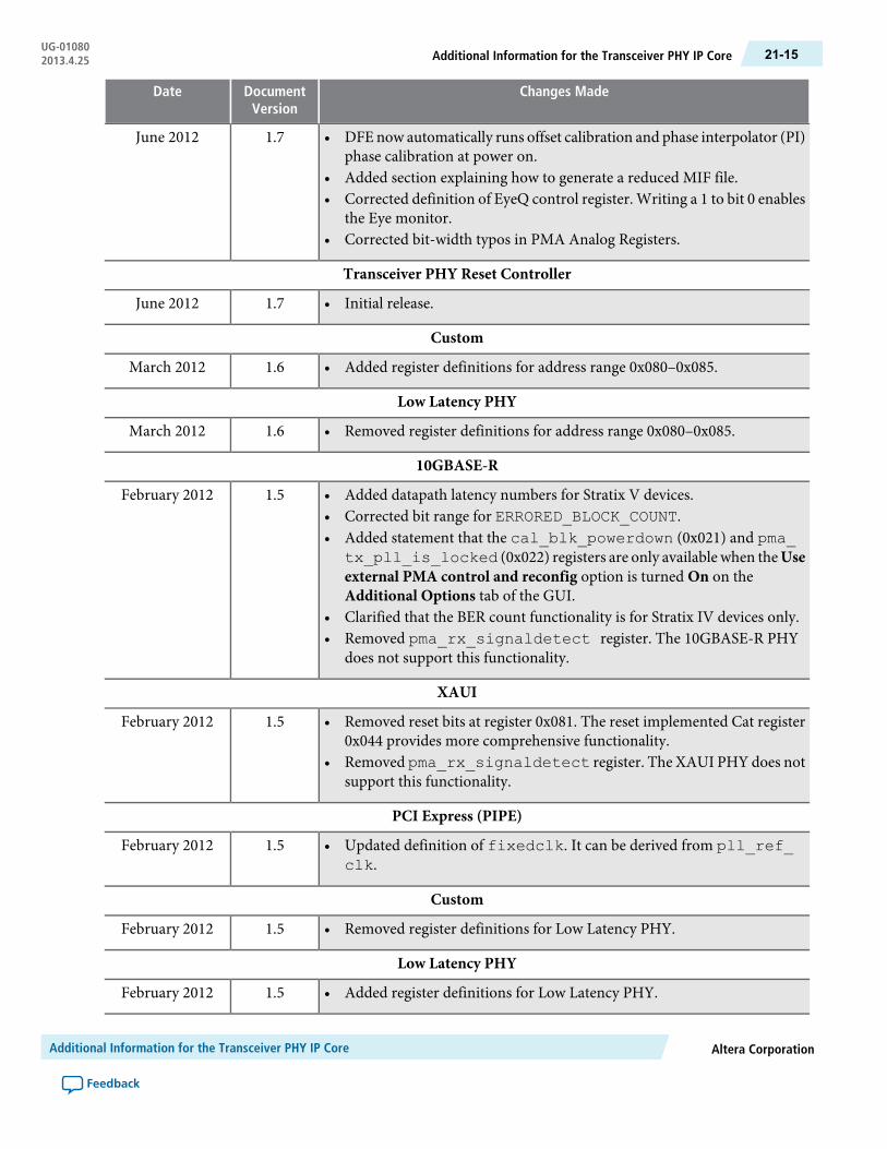
Changes MadeDocumentVersion
Date
• DFEnow automatically runs offset calibration and phase interpolator (PI)phase calibration at power on.
• Added section explaining how to generate a reduced MIF file.• Corrected definition of EyeQ control register. Writing a 1 to bit 0 enables
the Eye monitor.• Corrected bit-width typos in PMA Analog Registers.
1.7June 2012
Transceiver PHY Reset Controller
• Initial release.1.7June 2012
Custom
• Added register definitions for address range 0x080–0x085.1.6March 2012
Low Latency PHY
• Removed register definitions for address range 0x080–0x085.1.6March 2012
10GBASE-R
• Added datapath latency numbers for Stratix V devices.• Corrected bit range for ERRORED_BLOCK_COUNT.• Added statement that the cal_blk_powerdown (0x021) and pma_
tx_pll_is_locked (0x022) registers are only available when theUseexternal PMA control and reconfig option is turned On on theAdditional Options tab of the GUI.
• Clarified that the BER count functionality is for Stratix IV devices only.• Removed pma_rx_signaldetect register. The 10GBASE-R PHY
does not support this functionality.
1.5February 2012
XAUI
• Removed reset bits at register 0x081. The reset implemented Cat register0x044 provides more comprehensive functionality.
• Removed pma_rx_signaldetect register. The XAUI PHY does notsupport this functionality.
1.5February 2012
PCI Express (PIPE)
• Updated definition of fixedclk. It can be derived from pll_ref_clk.
1.5February 2012
Custom
• Removed register definitions for Low Latency PHY.1.5February 2012
Low Latency PHY
• Added register definitions for Low Latency PHY.1.5February 2012
Altera CorporationAdditional Information for the Transceiver PHY IP Core
Feedback
21-15Additional Information for the Transceiver PHY IP CoreUG-010802013.4.25
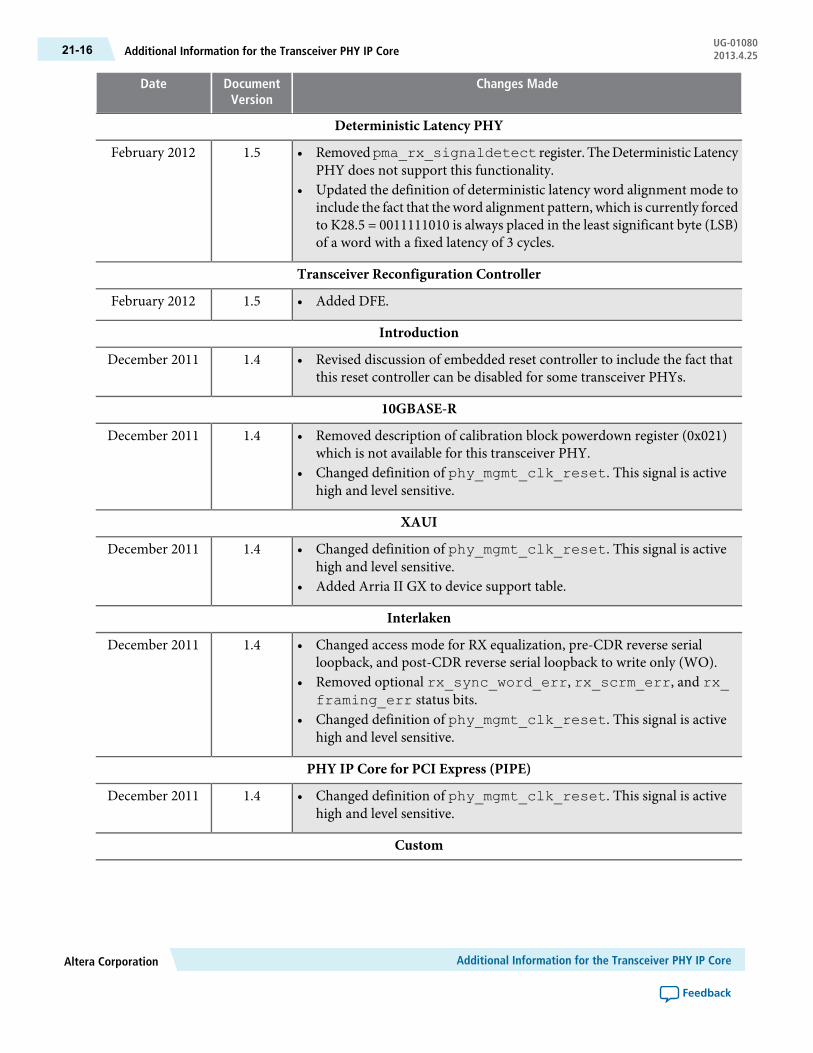
Changes MadeDocumentVersion
Date
Deterministic Latency PHY
• Removedpma_rx_signaldetect register. TheDeterministic LatencyPHY does not support this functionality.
• Updated the definition of deterministic latency word alignment mode toinclude the fact that the word alignment pattern, which is currently forcedto K28.5 = 0011111010 is always placed in the least significant byte (LSB)of a word with a fixed latency of 3 cycles.
1.5February 2012
Transceiver Reconfiguration Controller
• Added DFE.1.5February 2012
Introduction
• Revised discussion of embedded reset controller to include the fact thatthis reset controller can be disabled for some transceiver PHYs.
1.4December 2011
10GBASE-R
• Removed description of calibration block powerdown register (0x021)which is not available for this transceiver PHY.
• Changed definition of phy_mgmt_clk_reset. This signal is activehigh and level sensitive.
1.4December 2011
XAUI
• Changed definition of phy_mgmt_clk_reset. This signal is activehigh and level sensitive.
• Added Arria II GX to device support table.
1.4December 2011
Interlaken
• Changed access mode for RX equalization, pre-CDR reverse serialloopback, and post-CDR reverse serial loopback to write only (WO).
• Removed optional rx_sync_word_err, rx_scrm_err, and rx_framing_err status bits.
• Changed definition of phy_mgmt_clk_reset. This signal is activehigh and level sensitive.
1.4December 2011
PHY IP Core for PCI Express (PIPE)
• Changed definition of phy_mgmt_clk_reset. This signal is activehigh and level sensitive.
1.4December 2011
Custom
Additional Information for the Transceiver PHY IP CoreAltera Corporation
Feedback
UG-01080Additional Information for the Transceiver PHY IP Core21-16 2013.4.25

Changes MadeDocumentVersion
Date
• Added ×N and feedback compensation options for bonded clocks.• AddedEnableChannel Interfaceparameterwhich is required for dynamic
reconfiguration of transceivers.• Corrected formulas for signal width in top-level signals figure.• Changed definition of phy_mgmt_clk_reset. This signal is active
high and level sensitive.
1.4December 2011
Low Latency PHY
• Added option to disable the embedded reset controller to allow you tocreate your own reset sequence.
• Added ×N and feedback compensation options for bonded clocks.• Fixednameofphy_mgmt_reset signal. Should bephy_mgmt_clk_
reset. Also, a positive edge on this signal initiates a reset.• AddedEnableChannel Interfaceparameterwhich is required for dynamic
reconfiguration of transceivers.• Corrected formulas for signal width in top-level signals figure.• Changed definition of phy_mgmt_clk_reset. This signal is active
high and level sensitive.
1.4December 2011
Deterministic Latency PHY
• Removed Enable tx_clkout feedback path for TXPLL from the GeneralOptions tab of the Deterministic Latency PHY IP Core GUI. This optionis unavailable in 11.1 and 11.1 SP1.
• Changed definition of phy_mgmt_clk_reset. This signal is activehigh and level sensitive.
1.4December 2011
Transceiver Reconfiguration Controller
• Added duty cycle distortion (DCD) signal integrity feature.• Added PLL and channel reconfiguration using a memory initialization
file (.mif).• Added ability to reconfigure PLLs, including the input reference clock or
to change the PLL that supplies the high speed serial clock to the serializerwithout including logic to reconfigure channels.
• Corrected values for RX equalization gain. 0–4 are available.• Corrected logical number in InterfaceOrderingwithMultiple Transceiver
PHY Instances.• Increased the number of channels that can share a PLL from 5 to 11 when
feedback compensation is used.• Increased the number of channels that can connect to the Transceiver
Reconfiguration Controller from 32 to 64.• Added section on requirements for merging PLLs.
1.4December 2011
Introduction
Altera CorporationAdditional Information for the Transceiver PHY IP Core
Feedback
21-17Additional Information for the Transceiver PHY IP CoreUG-010802013.4.25
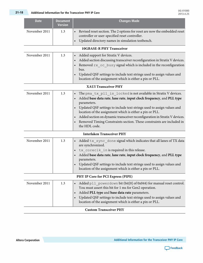
Changes MadeDocumentVersion
Date
• Revised reset section. The 2 options for reset are now the embedded resetcontroller or user-specified reset controller.
• Updated directory names in simulation testbench.
1.3November 2011
10GBASE-R PHY Transceiver
• Added support for Stratix V devices.• Added section discussing transceiver reconfiguration in Stratix V devices.• Removed rx_oc_busy signal which is included in the reconfiguration
bus.• Updated QSF settings to include text strings used to assign values and
location of the assignment which is either a pin or PLL.
1.3November 2011
XAUI Transceiver PHY
• The pma_tx_pll_is_locked is not available in Stratix V devices.• Added base data rate, lane rate, input clock frequency, and PLL type
parameters.• Updated QSF settings to include text strings used to assign values and
location of the assignment which is either a pin or PLL.• Added section ondynamic transceiver reconfiguration in StratixVdevices.• Removed Timing Constraints section. These constraints are included in
the HDL code.
1.3November 2011
Interlaken Transceiver PHY
• Added tx_sync_done signal which indicates that all lanes of TX dataare synchronized.
• tx_coreclk_in is required in this release.• Added base data rate, lane rate, input clock frequency, and PLL type
parameters.• Updated QSF settings to include text strings used to assign values and
location of the assignment which is either a pin or PLL.
1.3November 2011
PHY IP Core for PCI Express (PIPE)
• Added pll_powerdown bit (bit[0] of 0x044) for manual reset control.You must assert this bit for 1 ms for Gen2 operation.
• Added PLL type and base data rate parameters.• Updated QSF settings to include text strings used to assign values and
location of the assignment which is either a pin or PLL.
1.3November 2011
Custom Transceiver PHY
Additional Information for the Transceiver PHY IP CoreAltera Corporation
Feedback
UG-01080Additional Information for the Transceiver PHY IP Core21-18 2013.4.25

Changes MadeDocumentVersion
Date
• Added Arria V and Cyclone V support.• Addedbase data rate, lane rate, input clock frequency, and PLL type
parameters.• Revised reset options. The 2 options for reset are now the embedded reset
controller or a user-specified reset logic.• Updated QSF settings to include text strings used to assign values and
location of the assignment which is either a pin or PLL.
1.3November 2011
Low Latency PHY
• Added base data rate, lane rate, input clock frequency, and PLL typeparameters.
• Updated QSF settings to include text strings used to assign values andlocation of the assignment which is either a pin or PLL.
• Revised reset options. The 2 options for reset are now the embedded resetcontroller or a user-specified reset logic.
1.3November 2011
Deterministic Latency
• Initial release.1.3November 2011
Transceiver Reconfiguration Controller
• Added MIF support to allow transceiver reconfiguration from a .mif filethat may contain updates to multiple settings.
• Added support for the following features:• EyeQ• AEQ• ATX tuning• PLL reconfiguration• DC gain and four-stage linear equalization for the RX channels• Removed Stratix IV device support.• Changed frequency range of phy_mgmt_clk to 100-125 MHz.
1.3November 2011
All Chapters
Altera CorporationAdditional Information for the Transceiver PHY IP Core
Feedback
21-19Additional Information for the Transceiver PHY IP CoreUG-010802013.4.25
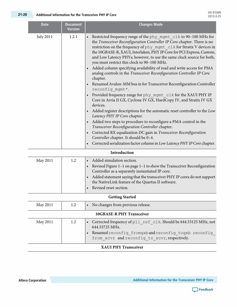
Changes MadeDocumentVersion
Date
• Restricted frequency range of the phy_mgmt_clk to 90–100 MHz forthe Transceiver Reconfiguration Controller IP Core chapter. There is norestriction on the frequency of phy_mgmt_clk for Stratix V devices inthe 10GBASE-R,XAUI, Interlaken, PHY IPCore for PCIExpress, Custom,and Low Latency PHYs; however, to use the same clock source for both,you must restrict this clock to 90–100 MHz.
• Added column specifying availability of read and write access for PMAanalog controls in the Transceiver Reconfiguration Controller IP Corechapter.
• RenamedAvalon-MMbus in for Transceiver ReconfigurationControllerreconfig_mgmt*.
• Provided frequency range for phy_mgmt_clk for the XAUI PHY IPCore in Arria II GX, Cyclone IV GX, HardCopy IV, and Stratix IV GXdevices.
• Added register descriptions for the automatic reset controller to the LowLatency PHY IP Core chapter.
• Added two steps to procedure to reconfigure a PMA control in theTransceiver Reconfiguration Controller chapter.
• Corrected RX equalization DC gain in Transceiver ReconfigurationController chapter. It should be 0–4.
• Corrected serialization factor column inLowLatency PHY IPCore chapter.
1.2.1July 2011
Introduction
• Added simulation section.• Revised Figure 1–1 on page 1–1 to show the Transceiver Reconfiguration
Controller as a separately instantiated IP core.• Added statement saying that the transceiver PHY IP cores do not support
the NativeLink feature of the Quartus II software.• Revised reset section.
1.2May 2011
Getting Started
• No changes from previous release.1.2May 2011
10GBASE-R PHY Transceiver
• Corrected frequency of pll_ref_clk. Should be 644.53125 MHz, not644.53725 MHz.
• Renamedreconfig_fromgxbandreconfig_togxb reconfig_from_xcvr and reconfig_to_xcvr, respectively.
1.2May 2011
XAUI PHY Transceiver
Additional Information for the Transceiver PHY IP CoreAltera Corporation
Feedback
UG-01080Additional Information for the Transceiver PHY IP Core21-20 2013.4.25
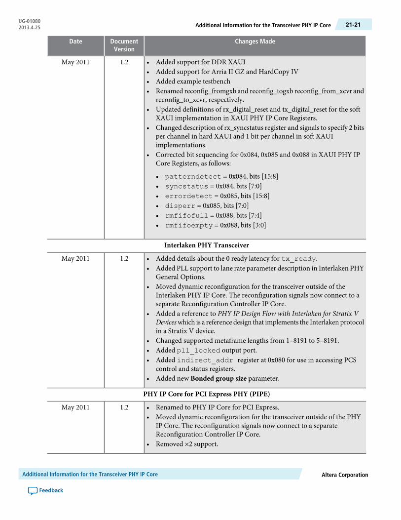
Changes MadeDocumentVersion
Date
• Added support for DDR XAUI• Added support for Arria II GZ and HardCopy IV• Added example testbench• Renamed reconfig_fromgxb and reconfig_togxb reconfig_from_xcvr and
reconfig_to_xcvr, respectively.• Updated definitions of rx_digital_reset and tx_digital_reset for the soft
XAUI implementation in XAUI PHY IP Core Registers.• Changed description of rx_syncstatus register and signals to specify 2 bits
per channel in hard XAUI and 1 bit per channel in soft XAUIimplementations.
• Corrected bit sequencing for 0x084, 0x085 and 0x088 in XAUI PHY IPCore Registers, as follows:
• patterndetect = 0x084, bits [15:8]• syncstatus = 0x084, bits [7:0]• errordetect = 0x085, bits [15:8]• disperr = 0x085, bits [7:0]• rmfifofull = 0x088, bits [7:4]• rmfifoempty = 0x088, bits [3:0]
1.2May 2011
Interlaken PHY Transceiver
• Added details about the 0 ready latency for tx_ready.• Added PLL support to lane rate parameter description in Interlaken PHY
General Options.• Moved dynamic reconfiguration for the transceiver outside of the
Interlaken PHY IP Core. The reconfiguration signals now connect to aseparate Reconfiguration Controller IP Core.
• Added a reference to PHY IP Design Flow with Interlaken for Stratix VDeviceswhich is a reference design that implements the Interlaken protocolin a Stratix V device.
• Changed supported metaframe lengths from 1–8191 to 5–8191.• Added pll_locked output port.• Added indirect_addr register at 0x080 for use in accessing PCS
control and status registers.• Added new Bonded group size parameter.
1.2May 2011
PHY IP Core for PCI Express PHY (PIPE)
• Renamed to PHY IP Core for PCI Express.• Moved dynamic reconfiguration for the transceiver outside of the PHY
IP Core. The reconfiguration signals now connect to a separateReconfiguration Controller IP Core.
• Removed ×2 support.
1.2May 2011
Altera CorporationAdditional Information for the Transceiver PHY IP Core
Feedback
21-21Additional Information for the Transceiver PHY IP CoreUG-010802013.4.25
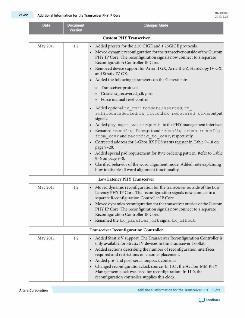
Changes MadeDocumentVersion
Date
Custom PHY Transceiver
• Added presets for the 2.50 GIGE and 1.25GIGE protocols.• Moved dynamic reconfiguration for the transceiver outside of the Custom
PHY IP Core. The reconfiguration signals now connect to a separateReconfiguration Controller IP Core.
• Removed device support for Arria II GX, Arria II GZ, HardCopy IV GX,and Stratix IV GX.
• Added the following parameters on the General tab:
• Transceiver protocol• Create rx_recovered_clk port• Force manual reset control
• Added optional rx_rmfifoddatainserted, rx_rmfifodatadelted,rx_rlv, andrx_recovered_clk as outputsignals.
• Addedphy_mgmt_waitrequest to the PHYmanagement interface.• Renamedreconfig_fromgxbandreconfig_togxb reconfig_
from_xcvr and reconfig_to_xcvr, respectively.• Corrected address for 8-Gbps RX PCS status register in Table 9–18 on
page 9–20.• Added special pad requirement for Byte ordering pattern. Refer to Table
9–6 on page 9–8.• Clarified behavior of the word alignment mode. Added note explaining
how to disable all word alignment functionality.
1.2May 2011
Low Latency PHY Transceiver
• Moved dynamic reconfiguration for the transceiver outside of the LowLatency PHY IP Core. The reconfiguration signals now connect to aseparate Reconfiguration Controller IP Core.
• Moveddynamics reconfiguration for the transceiver outside of theCustomPHY IP Core. The reconfiguration signals now connect to a separateReconfiguration Controller IP Core.
• Renamed the tx_parallel_clk signal tx_clkout.
1.2May 2011
Transceiver Reconfiguration Controller
• Added Stratix V support. The Transceiver Reconfiguration Controller isonly available for Stratix IV devices in the Transceiver Toolkit.
• Added sections describing the number of reconfiguration interfacesrequired and restrictions on channel placement.
• Added pre- and post-serial loopback controls.• Changed reconfiguration clock source. In 10.1, the Avalon-MM PHY
Management clock was used for reconfiguration. In 11.0, thereconfiguration controller supplies this clock.
1.2May 2011
Additional Information for the Transceiver PHY IP CoreAltera Corporation
Feedback
UG-01080Additional Information for the Transceiver PHY IP Core21-22 2013.4.25

Changes MadeDocumentVersion
Date
Migrating from Stratix IV to Stratix V
• Added discussion of dynamic reconfiguration for Stratix IV and StratixV devices.
• Added information on loopbackmodes for Stratix IV and StratixVdevices.• Added new parameters for Custom PHY IP Core in Stratix V devices.
1.2May 2011
All Chapters
• Corrected frequency range for thephy_mgmt_clk for the CustomPHYIP Core in Avalon-MM PHY Management Interface.
• Added optional reconfig_from_xcvr[67:0] to XAUI Top-LevelSignals—Soft PCS andPMA. Providedmore detail on size ofreconfig_from_xcvr inDynamic Reconfiguration InterfaceArria II GX, CycloneIV GX, HardCopy IV GX, and Stratix IV GX devices.
• Removed table providing ordering codes for the Interlaken PHY IP Core.Ordering codes are not required for Stratix V devices using the hardimplementation of the Interlaken PHY.
• Added note to 10GBASE-R release information table stating that “Noordering codes or license files are required for Stratix V devices.”
• Minor update to the steps to reconfigure a TX or RX PMA setting in theTransceiver Reconfiguration Controller chapter.
1.11December 2010
Introduction
• Revised reset diagram.• Added block diagram for reset.• Removed support for SOPC Builder.
1.1December 2010
Getting Started
• Removed description of SOPC Builder design flow. SOPC Builder is notsupported in this release.
1.1December 2010
10GBASE-R PHY Transceiver
• • Added Stratix V support• Changed phy_mgmt_address from 16 to 9 bits.• Renamed management interface, adding phy_ prefix• Renamed block_lock and hi_ber signals rx_block_lock
and rx_hi_ber, respectively.• Added top-level signals for external PMA and reconfiguration
controller in Stratix IV devices. Refer to External PMA andReconfiguration Signals.
• Removed the mgmt_burstcount signal.• Changed register map to show word addresses instead of a byte offset
from a base address.
1.1December 2010
Altera CorporationAdditional Information for the Transceiver PHY IP Core
Feedback
21-23Additional Information for the Transceiver PHY IP CoreUG-010802013.4.25

Changes MadeDocumentVersion
Date
XAUI PHY Transceiver
• Added support for Arria II GX and Cyclone IV GX with hard PCS• Renamed management interface, adding phy_ prefix• Changed phy_mgmt_address from 16 to 9 bits.• Renamed many signals. Refer to XAUI Top-Level Signals—Soft PCS and
PMA and “XAUI Top-Level Signals–Hard IP PCS and PMA” asappropriate.
• Changed register map to show word addresses instead of a byte offsetfrom a base address.
• Removed the rx_ctrldetect and rx_freqlocked signals.
1.1December 2010
Interlaken PHY Transceiver
• Added simulation support in ModelSim SE, Synopsys VCS MX, CadenceNCSim
• Changed number of lanes supported from 4–24 to 1–24.• Changed reference clock to be 1/20th rather than 1/10th the lane rate.• Renamed management interface, adding phy_ prefix• Changed phy_mgmt_address from 16 to 9 bits.• Changed many signal names, refer to Top-Level Interlaken PHY
Signals.Changed register map to show word addresses instead of a byteoffset from a base address.
1.1December 2010
PCI Express PHY (PIPE)
• Added simulation support in ModelSim SE• Added PIPE low latency configuration option• Changed phy_mgmt_address from 16 to 9 bits.• Changed register map to show word addresses instead of a byte offset
from a base address.• Added tx_ready, rx_ready, pipe_txswing, and pipe_
rxeleciidle signals• Added rx_errdetect, rx_disperr, and rx_a1a2sizeout
register fields
1.1December 2010
Custom PHY Transceiver
Additional Information for the Transceiver PHY IP CoreAltera Corporation
Feedback
UG-01080Additional Information for the Transceiver PHY IP Core21-24 2013.4.25

Changes MadeDocumentVersion
Date
• Added support for 8B/10B encoding and decoding in Stratix V devices• Added support for rate matching in Stratix V devices.• Added support for Arria II GX, Arria II GZ,HardCopy IVGX, and Stratix
IV GX devices• Changed phy_mgmt_address from 8 to 9 bits.• Added many optional status ports and renamed some signals. Refer to
Figure 9–2 on page 9–15 and subsequent signal descriptions.• Changed register map to show word addresses instead of a byte offset
from a base address.
1.1December 2010
Low Latency PHY IP Core
• Renamed management interface, adding phy_ prefix• Changed phy_mgmt_address from 16 to 9 bits.• Changed register map to show word addresses instead of a byte offset
from a base address.• Removed rx_offset_cancellation_done signal. Internal reset
logic determines when offset cancellation has completed.• Removed support for Stratix IV GX devices.
1.1December 2010
Transceiver Reconfiguration Controller
• Reconfiguration is now integrated into the XAUI PHY IP Core and10GBASE-R PHY IP Core.
• Revised register map to show word addresses instead of a byte offset froma base address.
1.1December 2010
Migrating from Stratix IV to Stratix V
• Changed phy_mgmt_address from 16 to 9 bits.1.1December 2010
• Corrected address offsets in PMAAnalog Registers. These are byte offsetsand should be: 0x00, 0x04, 0x08, 0x0C, 0x10, not 0x00, 0x01, 0x02, 0x03,0x04.
• Corrected base address for transceiver reconfiguration control and statusregisters in PMA Analog Registers. It should be 0x420, not 0x400.
• Corrected byte offsets in Custom PHY IP Core Registers and PCI ExpressPHY (PIPE) IP Core Registers. The base address is 0x200. The offsets are0x000–0x018.
1.1November 2010
• Initial release.1.0July 2010
How to Contact AlteraThis section provides the contact information for Altera.
Altera CorporationAdditional Information for the Transceiver PHY IP Core
Feedback
21-25How to Contact AlteraUG-010802013.4.25

Table 21-1: Altera Contact Information
AddressContact MethodContact15
www.altera.com/supportWebsiteTechnical support
www.altera.com/trainingWebsiteTechnical training
www.altera.com/literatureWebsiteProduct literature
[email protected] support
[email protected] licensing
Related Informationwww.altera.com/support
www.altera.com/training
www.altera.com/literature
15 You can also contact your local Altera sales office or sales representative.
Additional Information for the Transceiver PHY IP CoreAltera Corporation
Feedback
UG-01080How to Contact Altera21-26 2013.4.25