advanced synthesis cookbook - digchipapplication-notes.digchip.com/038/38-21447.pdf · advanced...
TRANSCRIPT

101 Innovation DriveSan Jose, CA 95134(408) 544-7000www.altera.com
Advanced Synthesis Cookbook:A Design Guide for Stratix II, Stratix III,
and Stratix IV Devices
Software Version: 8.0Document Version: 3.0Document Date: May 2008MNL-01017-3.0

Copyright © 2007 Altera Corporation. All rights reserved. Altera, The Programmable Solutions Company, the stylized Altera logo, specific device des-ignations, and all other words and logos that are identified as trademarks and/or service marks are, unless noted otherwise, the trademarks andservice marks of Altera Corporation in the U.S. and other countries. All other product or service names are the property of their respective holders. Al-tera products are protected under numerous U.S. and foreign patents and pending applications, maskwork rights, and copyrights. Altera warrantsperformance of its semiconductor products to current specifications in accordance with Altera's standard warranty, but reserves the right to makechanges to any products and services at any time without notice. Altera assumes no responsibility or liability arising out of the ap-plication or use of any information, product, or service described herein except as expressly agreed to in writing by AlteraCorporation. Altera customers are advised to obtain the latest version of device specifications before relying on any published in-formation and before placing orders for products or services.
ii MegaCore Version a.b.c variable Altera CorporationMay 2008
MNL-01017-3.0
Altera Corporation iii
Contents
About this User Guide ............................................................................ vii
Introduction ......................................................................................... 1Blocks and Techniques .......................................................................................................................... 1–1Simulating the Examples ...................................................................................................................... 1–1Using C Compiler .................................................................................................................................. 1–2
Chapter 1. ArithmeticIntroduction ............................................................................................................................................ 1–3Basic Addition ........................................................................................................................................ 1–4Ternary Addition ................................................................................................................................... 1–4Grouping Ternary Adders .................................................................................................................... 1–5Double Addsub/ Basic Addsub .......................................................................................................... 1–5
Two’s Complement Arithmetic Review ....................................................................................... 1–5Traditional ADDSUB Unit .............................................................................................................. 1–6
Compressors (Carry Save Adders) ..................................................................................................... 1–6Compressor Width 6:3 ..................................................................................................................... 1–6Compressor Width 3:2 ..................................................................................................................... 1–7Combining Compressors (Compressor Width 4:2) ..................................................................... 1–7
Bit Population Count ............................................................................................................................. 1–8Splitting Adder Chains ......................................................................................................................... 1–8Pipelined Adder Chains ....................................................................................................................... 1–9Carry Select Adders ............................................................................................................................... 1–9Adder Trees .......................................................................................................................................... 1–10Basic Multiplication ............................................................................................................................. 1–11Multiplication With Rotate and Shift Modes ................................................................................... 1–11High-Speed LCell-Based Multiplication .......................................................................................... 1–12Multiplication of Large Integers (Karatsuba Algorithm) .............................................................. 1–14Division (Unsigned Integer) ............................................................................................................... 1–17
Chapter 2. Floating Point TricksFloating Point to Fixed Point Conversion ........................................................................................ 2–19Approximate Square Root .................................................................................................................. 2–20Approximate Inverse Square Root .................................................................................................... 2–20
Chapter 3. Translation and Format ConversionOne-Hot to Binary ............................................................................................................................... 3–23Binary-to-Gray Conversion ................................................................................................................ 3–24Gray-To-Binary Conversion ............................................................................................................... 3–25Seven Segment Display Driver .......................................................................................................... 3–25

iv Altera Corporation
Contents
Binary-to-ASCII Hexadecimal Conversion ...................................................................................... 3–26ASCII Hexadecimal-to-Binary Conversion ...................................................................................... 3–26Binary-to-Decimal/Binary-Coded Decimal Adders ...................................................................... 3–27
Chapter 4. VideoYCbCr (4:4:4) to RGB Conversion ..................................................................................................... 4–29RGB to Hue Conversion ..................................................................................................................... 4–29Sum of Absolute Difference (SAD) ................................................................................................... 4–30VGA Monitor Control ......................................................................................................................... 4–31
Chapter 5. ArbitrationBitscan (Priority Masking) .................................................................................................................. 5–33Arbiters with Fairness ......................................................................................................................... 5–33Priority Encoding ................................................................................................................................. 5–34
Chapter 6. MultiplexingBasic Multiplexing (Binary Encoded) ............................................................................................... 6–35If/Else Multiplexing (?: Multiplexing) ............................................................................................. 6–37Priority Multiplexing .......................................................................................................................... 6–388-to-1 Multiplex Building Blocks ....................................................................................................... 6–39Barrel Shift ............................................................................................................................................ 6–39Use of Register Secondary Signals for Multiplexing ...................................................................... 6–41Bus Multiplexing ................................................................................................................................. 6–42Pipelined Bus Multiplexing ................................................................................................................ 6–42
Chapter 7. Comparison and Adder DetectionBus Equality ( A == B ) ............................................................................................................................................... 7–43Mapping Wide Single-Output Functions to the Carry Chain ....................................................... 7–43Equal to Constant ................................................................................................................................ 7–44Less than Constant .............................................................................................................................. 7–45Address in Range Comparison (LOWER <= addr < UPPER) ....................................................... 7–45Match or Inverse Match ...................................................................................................................... 7–47
Chapter 8. Registers and MemoriesRegister Banks ...................................................................................................................................... 8–4924-Bit/16-Bit Stream Buffers (RGB/Memory Buffer) ..................................................................... 8–50RAM-Based Shift Register .................................................................................................................. 8–50Simple Quad Port RAM ...................................................................................................................... 8–52Ternary Content Addressable Memory (TCAM) ............................................................................ 8–53
Register-Based Ternary CAM ....................................................................................................... 8–54RAM-Based Ternary CAM ............................................................................................................ 8–55
Chapter 9. CountersBasic Binary Counter ........................................................................................................................... 9–57Up/Down Counter .............................................................................................................................. 9–57
Altera Corporation v
Contents
Modulus Counter with Lookahead ................................................................................................... 9–58
Chapter 10. Communication8B10B Encoder/ Decoder ................................................................................................................. 10–63Universal Asynchronous Receiver Transmitter (UART) ............................................................. 10–65
Chapter 11. Cyclic Redundancy CheckIntroduction ........................................................................................................................................ 11–67CRC XOR Decomposition ................................................................................................................ 11–68CRC-16 Fixed Data Width ................................................................................................................ 11–69CRC-32 Fixed Data Width ................................................................................................................ 11–69CRC-32 Variable Data Width (Residues) ....................................................................................... 11–69CRC-32 Ethernet FCS ........................................................................................................................ 11–70
Chapter 12. Error Correction Codes64/72-Bit ECC Encoder/ Decoder .................................................................................................. 12–7164/72-Bit ECC Dual-Port Internal RAM ........................................................................................ 12–73ECC 32/39-Bit Variation ................................................................................................................... 12–74ECC 16/22-Bit Variation ................................................................................................................... 12–74ECC 8/13-Bit Variation ..................................................................................................................... 12–74Reed-Solomon Forward Error Correction (FEC) .......................................................................... 12–75
Reed-Solomon Transmitter ......................................................................................................... 12–75Reed-Solomon Receiver ............................................................................................................... 12–76Galois Field Multiplication ......................................................................................................... 12–78
Chapter 13. Random and Pseudorandom FunctionsLinear Feedback Shift Register ........................................................................................................ 13–81Built-In Logic Block Observer .......................................................................................................... 13–81C Library Random Number Generator .......................................................................................... 13–82True Random Numbers .................................................................................................................... 13–82
Race Condition-Based True Random Numbers ...................................................................... 13–83Word Stream Scrambling ................................................................................................................. 13–86
Chapter 14. CryptographyData Encryption Standard ................................................................................................................ 14–89Triple DES ........................................................................................................................................... 14–91UNIX Password Encryption ............................................................................................................. 14–91Advanced Encryption Standard/ Rijndael .................................................................................... 14–92
The Rijndael S-BOX/sub_bytes .................................................................................................. 14–93Rijndael shift_rows ....................................................................................................................... 14–94Rijndael mix_columns and Round Keying ............................................................................... 14–94Rijndael Key Evolution ................................................................................................................ 14–95Rijndael 128 Encipher .................................................................................................................. 14–95Rijndael 128 Decipher .................................................................................................................. 14–96Rijndael 256-Bit Key Size (AES 256) .......................................................................................... 14–96Rijndael 192-Bit Key Size (AES 192) .......................................................................................... 14–96

vi Altera Corporation
Contents
RC4 Stream ......................................................................................................................................... 14–97Secure Hash Algorithm .................................................................................................................... 14–97
Chapter 15. SynchronizationSystem Reset Control ........................................................................................................................ 15–99Clock Multiplexing .......................................................................................................................... 15–102
Altera Corporation MegaCore Version a.b.c variablevii
About this User Guide
Revision History The table below displays the revision history for the chapters in this User Guide.
How to Contact Altera
For the most up-to-date information about Altera® products, refer to the following table.
Date/Version Changes Made Summary of Changes
May 2007, v1.0 Initial release.
October 2007, v2.0 Added new sections. Added the following sections:● “Multiplication of Large Integers
(Karatsuba Algorithm)”● “Approximate Floating Point Divide (Single
Precision)”● “Ternary Content Addressable Memory
(TCAM)”● “Seconds Timer”
May 2008 Added new sections Added the following sections:● “True Random Numbers”● Chapter 15, Synchronization
Information Type Contact (1)
Technical support www.altera.com/mysupport/
Technical training www.altera.com/training/[email protected]
Product literature www.altera.com/literature/
Altera literature services [email protected]
FTP site ftp.altera.com
Note to table:(1) You can also contact your local Altera sales office or sales representative.

viii MegaCore Version a.b.c variable Altera Corporation
Typographic Conventions
Typographic Conventions
This document uses the typographic conventions shown below.
Visual Cue Meaning
Bold Type with Initial Capital Letters
Command names, dialog box titles, checkbox options, and dialog box options are shown in bold, initial capital letters. Example: Save As dialog box.
bold type External timing parameters, directory names, project names, disk drive names, file names, file name extensions, and software utility names are shown in bold type. Examples: fMAX, \qdesigns directory, d: drive, chiptrip.gdf file.
Italic Type with Initial Capital Letters
Document titles are shown in italic type with initial capital letters. Example: AN 75: High-Speed Board Design.
Italic type Internal timing parameters and variables are shown in italic type. Examples: tPIA, n + 1.
Variable names are enclosed in angle brackets (< >) and shown in italic type. Example: <file name>, <project name>.pof file.
Initial Capital Letters Keyboard keys and menu names are shown with initial capital letters. Examples: Delete key, the Options menu.
“Subheading Title” References to sections within a document and titles of online help topics are shown in quotation marks. Example: “Typographic Conventions.”
Courier type Signal and port names are shown in lowercase Courier type. Examples: data1, tdi, input. Active-low signals are denoted by suffix n, e.g., resetn.
Anything that must be typed exactly as it displays is shown in Courier type. For example: c:\qdesigns\tutorial\chiptrip.gdf. Also, sections of an actual file, such as a Report File, references to parts of files (e.g., the AHDL keyword SUBDESIGN), as well as logic function names (e.g., TRI) are shown in Courier.
1., 2., 3., anda., b., c., etc.
Numbered steps are used in a list of items when the sequence of the items is important, such as the steps listed in a procedure.
v, —, N/A Used in table cells to indicate the following: v indicates a “Yes” or “Applicable” statement; — indicates a “No” or “Not Supported” statement; N/A indicates that the table cell entry is not applicable to the item of interest.
■ ● • Bullets are used in a list of items when the sequence of the items is not important.
v The checkmark indicates a procedure that consists of one step only.
1 The hand points to information that requires special attention.
c A caution calls attention to a condition or possible situation that can damage or destroy the product or the user’s work.
w A warning calls attention to a condition or possible situation that can cause injury to the user.
r The angled arrow indicates you should press the Enter key.
f The feet direct you to more information on a particular topic.

Altera Corporation MegaCore Version a.b.c variable 1May 2008
Introduction
Blocks and Techniques
The Advanced Synthesis Cookbook is a collection of circuit building blocks and related discussions, and presumes you are familiar with Altera® hardware cells and the Quartus® II software tools. The Stratix® II logic cell is powerful, which helps the synthesis tools achieve good results without hand tuning. The cell features open up opportunities for dramatic hand-crafted “tricks.” These building blocks are intended to demonstrate these tricks.
f For more information about HDL coding styles, refer to the Recommended HDL Coding Styles chapter in volume 1 of the Quartus II Handbook. For more information about Stratix II device architecture, refer to the Stratix II Device Family Data Sheet section in volume 1 of the Stratix II Device Handbook.
Each section includes a list of example files. Many of these example files contain more than one method of implementation controlled by a parameter. You can use these example files for testing and to better understand the derivation of some of the more complex optimizations. There are also many cases where the ideal implementation depends on the surrounding circuitry. The discussion and comments should help with selection.
1 If you have a favorite optimization trick, or are struggling with a particular block of logic, file a mySupport request on the Altera website (www.altera.com/mysupport).
Simulating the Examples
Some of the examples in this document use WYSIWYG cells for direct mapping control. The Quartus II Integrated Synthesis and third-party synthesis tools automatically recognize WYSIWYG cells. To use the ModelSim simulator to simulate these examples, you must load the Stratix II atom library located in the <Quartus II installation directory>/eda/sim_lib directory. When you simulate the examples using the ModelSim simulator, you may receive an error similar to the following example:
Error: (vsim-3033) decoder_8b10b.v(351): Instantiation of ‘stratixii_lcell_comb’ failed. The design unit was not found.

2 MegaCore Version a.b.c variable Altera CorporationMay 2008
Using C Compiler
Type the following command in the ModelSim simulator at a system command prompt to correct this error (adjust to your quartus root location):
vlog d:/quartus/eda/sim_lib/stratixii_atoms.v r
Some of the examples in this document also use RAM or DSP megafunction blocks that are located in the altera_mf.v file in the <Quartus II installation directory>/eda/sim_lib directory.
Using C Compiler
Some of the examples in this document include small computer programs written in C (.CPP files). These programs generate Verilog HDL files provided for the interest of readers who may have some software background. Note that these C files are not directly useful for programming Altera devices or embedded processors.
The sample files listed in this document were originally compiled with Microsoft 32-bit C/C++ Optimizing Compiler Version 12.00.8804 for 80x86. The command line compile command is cl filename.cpp to create <filename>.exe. You can use the free Microsoft C Compiler Visual Studio Express Edition available from the Microsoft website.

Altera Corporation MegaCore Version a.b.c variable 1–3May 2008
Chapter 1. Arithmetic
Introduction The Stratix II logic cell contains a dedicated adder chain for fast carry propagation with optional logic on the input side (see Figure 1–1).
Figure 1–1. Stratix II Logic Cell
You can use the cell in shared arithmetic mode, which changes the input pattern to facilitate implementing 3:2 compressors in the LUT logic. Use shared mode to add three binary words in a single chain (see Figure 1–2).
Figure 1–2. Shared Arithmetic Mode
LUT 4
F0
dataa
datab
datac
datad
dataf
cin
sumout
coutshareout
LUT 4
F2
LUT 4
F2
+
LUT 4F0
dataadatabdatacdatad
cin
sumout
LUT 4F2
coutshareout
sharein
+
1–4 MegaCore Version a.b.c variable Altera CorporationMay 2008
Basic Addition
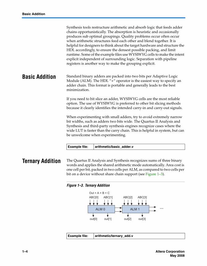
Synthesis tools restructure arithmetic and absorb logic that feeds adder chains opportunistically. The absorption is heuristic and occasionally produces sub optimal groupings. Quality problems occur often occur when arithmetic structures feed each other and blend together. It is helpful for designers to think about the target hardware and structure the HDL accordingly, to ensure the densest possible packing, and limit runtime. Some of the example files use WYSIWYG cells to make the intent explicit independent of surrounding logic. Separation with pipeline registers is another way to make the grouping explicit.
Basic Addition Standard binary adders are packed into two bits per Adaptive Logic Module (ALM). The HDL “+“ operator is the easiest way to specify an adder chain. This format is portable and generally leads to the best minimization.
If you need to bit slice an adder, WYSIWYG cells are the most reliable option. The use of WYSIWYG is preferred to other bit slicing methods because it clearly identifies the intended carry-in and carry-out signals.
When experimenting with small adders, try to avoid extremely narrow bit widths, such as adders two bits wide. The Quartus II Analysis and Synthesis and third-party synthesis engines recognize cases where the wide LUT is faster than the carry chain. This is helpful in system, but can be unwelcome when experimenting.
Ternary Addition The Quartus II Analysis and Synthesis recognizes sums of three binary words and applies the shared arithmetic mode automatically. Area cost is one cell per bit, packed in two cells per ALM, as compared to two cells per bit on a device without share chain support (see Figure 1–3).
Figure 1–3. Ternary Addition
Example file: arithmetic/basic_adder.v
Example file: arithmetic/ternary_add.v
ALM 0
ABC[0]Out = A + B + C
ABC[1]
ALM 1
ABC[2] ABC[3]
out[0] out[1] out[2] out[3]
…

Altera Corporation MegaCore Version a.b.c variable1–5May 2008
Arithmetic
Grouping Ternary Adders
When combining ternary additions with other arithmetic logic or as part of adder trees, it is best to place them in a submodule. Verilog HDL and VHDL consider “+“ a binary operator, potentially creating ambiguity about which adders to group as a ternary block. The example file ternary_sum_nine.v computes the sum of nine binary words using two levels of pipelined ternary adders (see Figure 1–4).
Figure 1–4. Grouping Ternary Adders
Double Addsub/ Basic Addsub
Apply the shared arithmetic mode to build a two-word add/subtract unit with independent sign control on each word. For example:
out = (negate_a ? –a[] : a[]) + (negate_b ? –b[] : b[]);
Two’s Complement Arithmetic Review
To negate a number in two’s complement form, invert the bits of the number, and then add 1. This process works in both directions. Negative numbers have a “1“ in the MSB (Figure 1–5).
Figure 1–5. Two’s Complement
You can implement (+/-A) as A when the sign is + and invert (A) + 1 when the sign is –. Because A and B are in the process of being summed, the +1s can be implemented at the same time (+0 when both are positive, +1 when exactly one is negative, and +2 when both are negative).
Example file: arithmetic/ternary_sum_nine.v
A B C
+
D E F
+
reg
+
G H I
+
reg reg reg
0 0 1 0 0 1
1 1 0 1 1 0
Invert
1 1 0 1 1 1
Add 1
0 0 1 0 0 1
1 1 0 1 1 1+
0 0 0 0 0 0
( 9 )( 9 )
( 0 )
( -9 )
( -9 )
1–6 MegaCore Version a.b.c variable Altera CorporationMay 2008
Compressors (Carry Save Adders)
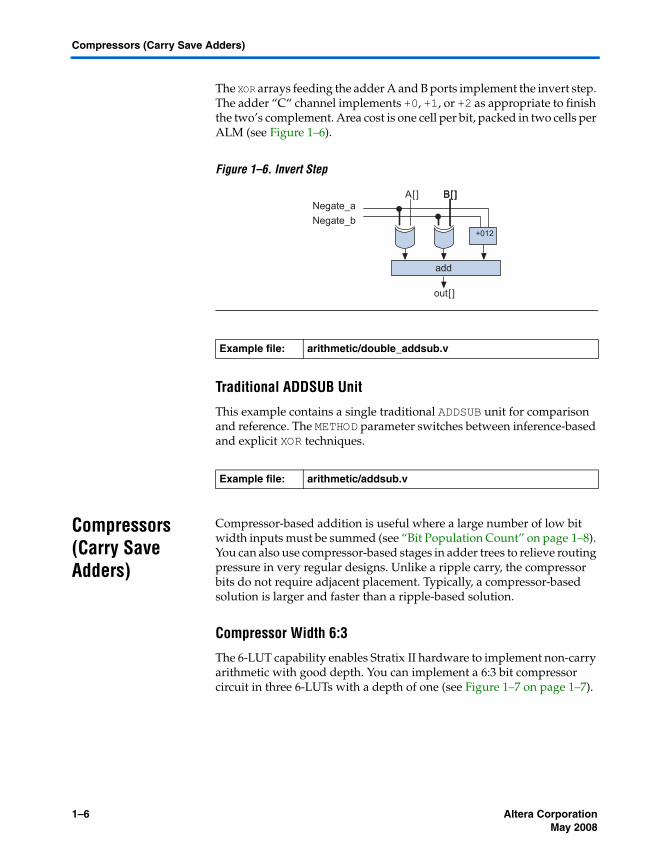
The XOR arrays feeding the adder A and B ports implement the invert step. The adder “C“ channel implements +0, +1, or +2 as appropriate to finish the two’s complement. Area cost is one cell per bit, packed in two cells per ALM (see Figure 1–6).
Figure 1–6. Invert Step
Traditional ADDSUB Unit
This example contains a single traditional ADDSUB unit for comparison and reference. The METHOD parameter switches between inference-based and explicit XOR techniques.
Compressors (Carry Save Adders)
Compressor-based addition is useful where a large number of low bit width inputs must be summed (see “Bit Population Count” on page 1–8). You can also use compressor-based stages in adder trees to relieve routing pressure in very regular designs. Unlike a ripple carry, the compressor bits do not require adjacent placement. Typically, a compressor-based solution is larger and faster than a ripple-based solution.
Compressor Width 6:3
The 6-LUT capability enables Stratix II hardware to implement non-carry arithmetic with good depth. You can implement a 6:3 bit compressor circuit in three 6-LUTs with a depth of one (see Figure 1–7 on page 1–7).
Example file: arithmetic/double_addsub.v
Example file: arithmetic/addsub.v
add
Negate_aNegate_b
A[] B[]B[]
out[ ]
+012
Altera Corporation MegaCore Version a.b.c variable1–7May 2008
Arithmetic
Figure 1–7. Three 6-LUTs With Depth One
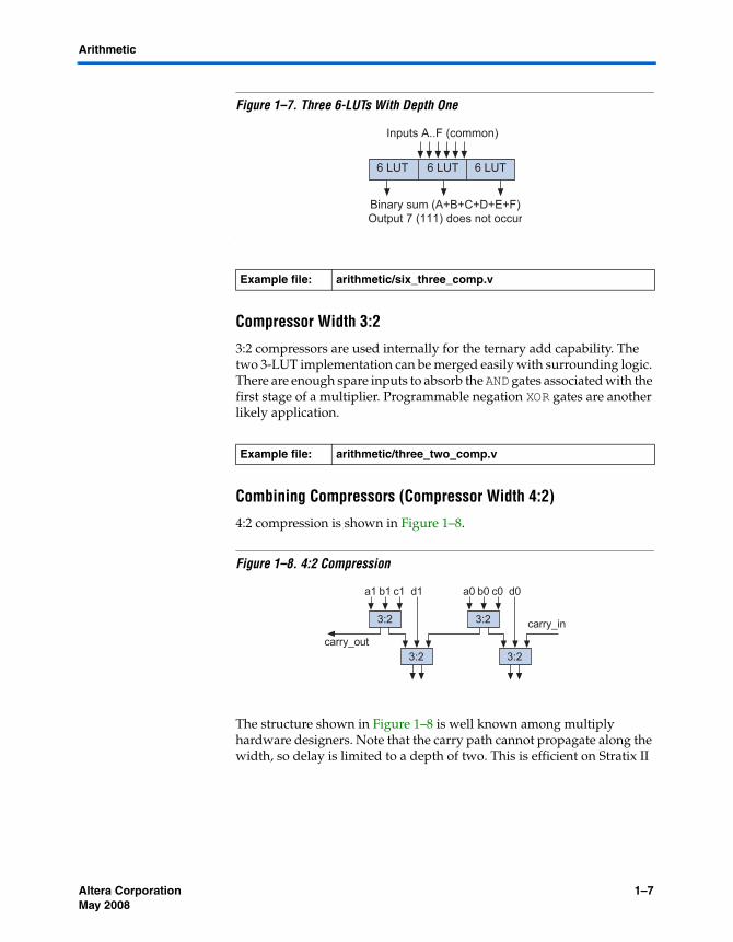
Compressor Width 3:2
3:2 compressors are used internally for the ternary add capability. The two 3-LUT implementation can be merged easily with surrounding logic. There are enough spare inputs to absorb the AND gates associated with the first stage of a multiplier. Programmable negation XOR gates are another likely application.
Combining Compressors (Compressor Width 4:2)
4:2 compression is shown in Figure 1–8.
Figure 1–8. 4:2 Compression
The structure shown in Figure 1–8 is well known among multiply hardware designers. Note that the carry path cannot propagate along the width, so delay is limited to a depth of two. This is efficient on Stratix II
Example file: arithmetic/six_three_comp.v
Example file: arithmetic/three_two_comp.v
Inputs A..F (common)
Binary sum (A+B+C+D+E+F)Output 7 (111) does not occur
6 LUT 6 LUT 6 LUT
3:2
3:2 carry_in
3:2
3:2
carry_out
a1 b1 c1 d1 a0 b0 c0 d0

1–8 MegaCore Version a.b.c variable Altera CorporationMay 2008
Bit Population Count
devices, although it does not fill the cells the way a 6:3 compressor does. The example design is left unstructured to allow flattening for speed, and can absorb input side logic such as multiplier AND gates.
Bit Population Count
An efficient method to count the number of ones or zeros in a binary word is to use compressors followed by an adder tree. The C-style method of using a “for“ loop with a shift and conditional +1 tends to create a stick-like structure which is difficult for the synthesis tools to interpret. In the best case, it requires a significant amount of runtime for analysis and balancing (see Figure 1–9).
Figure 1–9. Bit Population Count
The ideal crossover from compression to propagate addition is width specific. For bit width of 4 or 5 use propagate adders. For lower bit widths use compressors. The example thirtysix_six_comp.v shows a 36-input compressor suitable for bit population counting on 32-bit numbers.
Splitting Adder Chains
The Stratix II ALM contains a hard-wired adder chain to speed up the propagation of the carry signal for arithmetic functions. In some instances, it is desirable to break up a long chain by exiting the chain for one hop and then resuming, as shown in Figure 1–10.
Figure 1–10. Breaking Up a Long Chain
Example file: arithmetic/wide_compress.v
Example file: arithmetic/thirtysix_six_comp.v
Bit 0
Bit 1
Bit 2
Bit 3
Bit 4
6:3 6:3
…
…+
+
+
+
+
Further compressionif necessary
Final propagate add
6:3
ALBLAHBH
C+ +

Altera Corporation MegaCore Version a.b.c variable1–9May 2008
Arithmetic
Because wire C is on standard rather than carry chain routing, the adders (AL+BL) and (AH+BH) can be placed separately. For example, use this technique to relieve routing pressure on a long chain in where the L and H inputs are driven by separate sources. This technique does not always make the design faster, but it does simplify placement and routing. To accelerate long chains, see “Pipelined Adder Chains” on page 1–9.
Pipelined Adder Chains
Build a pipelined adder to accelerate a long carry chain when an extra tick of latency is available.
Figure 1–11. Pipelined Adder Chains
The example file implements the structure illustrated in Figure 1–11. It looks a bit odd due to the asymmetry of the high and low halves; however, it is equivalent to a simple adder followed by two registers. It is slightly less than twice as fast as an equivalent unpipelined adder.
Carry Select Adders
Carry select is a method of accelerating addition by supposing both possible carry in values, and then selecting the correct one. This technique is commonly used in computer hardware design (Figure 1–12).
Figure 1–12. Carry Select Adders
Example file: arithmetic/split_add.v
Example files: arithmetic/pipeline_add.varithmetic/pipeline_add_tb.v
ALBLAHBH
DQ+ +
DQ
DQDQ
DQDQ
+++
++ 0
1
0
1
A B A B A B
1–10 MegaCore Version a.b.c variable Altera CorporationMay 2008
Adder Trees
Stratix II ALM implementation requires about three times the area of a simple ripple carry, and is faster than a standard ripple on long chains. 40 bits is a reasonable guideline. The exact crossover point depends on the surrounding logic. In a bench test, a fully registered carry select on a 2S15C3 device ran at 317 MHz using four blocks of 14-bit ripple. The equivalent 56-bit pure ripple ran at 271 MHz.
The ripple length within a carry select block is a parameter to the example Verilog HDL. A typical setting for a Stratix II device is 14. This allows the adders to fit within single LABs with two bits of extra space. The extra positions are used to collect the carry out signal and to increase the flexibility for placing the carry out multiplexer. A small speed testing “jig” is included in the select_add_speed_test.v example file. Some experimentation may be required for the best block width setting at a given input size.
It is possible to use the SLOAD port to reduce the area cost from triple to double. There is a parameter in the example file that activates this feature; however, it appears to negate the speed advantage.
Adder Trees Adder trees are a common building block in digital filters and multipliers. They are typically implemented with high levels of pipeline. The ALM supports both binary and ternary adder trees. Roughly speaking, the ternary tree is one-half of the area of a binary tree, and has one-third fewer levels. Ternary trees are strongly favored in area-sensitive applications. When favoring speed, the pipelined binary tree is the more common method. The binary tree has a slightly lower carry delay within each adder due to lower function complexity. The cost decision can change depending on routing pressure in the surrounding circuitry and latency requirements.
This example is a parameterized binary adder tree. The input words for summation are concatenated to form the in_words bus. The parameters NUM_IN_WORDS x BITS_PER_IN_WORD control the size. The parameter OUT_BITS controls the expected result size. Some attempt is made to store intermediate results with the minimum number of bits (for example, 8 bits + 8 bits = 9 bits). The synthesis tools perform the remaining trimming. The Boolean parameter SIGN_EXT selects sign versus 0 extension for adding signed numbers. REGISTER_OUTPUT enables pipeline registers. When the REGISTER_OUTPUT value is 1, a pipeline register is inserted on the output of every adder node.
Example files: arithmetic/select_add.varithmetic/select_add_speed_test.v

Altera Corporation MegaCore Version a.b.c variable1–11May 2008
Arithmetic
REGISTER_MIDDLE enables additional registers embedded in the carry chains. This is intended for high speed applications where the carry propagation time within a word is too high.
The SHIFT_DIST parameter specifies a shift between input words. This is used for multiplication. SHIFT_DIST = 0 indicates simple addition of a list of numbers. The EXTRA_BIT parameter and the I/O signals are used to match the pipeline latency of an extra signal for convenience in signed multiplication. The lc_mult_signed example files use this adder in a multiplication context.
Basic Multiplication
Stratix II devices use native 36 x 36 multiply-accumulate (MAC) blocks to implement most multipliers. There is special hardware for packing 18x18 and 9x9 data widths. The report file lists the number of 9x9 DSP elements used. One 36x36 multiplier uses all 8 elements in the MAC block. You can access the basic multiplier through the Verilog HDL/VHDL “*“ operator or through the lpm_mult megafunction. The more complex output summation and accumulator modes are accessible through the altmult_add and altmult_accum megafunctions. Direct use of the underlying MAC_MULT and MAC_OUT WYSIWYG gates can be challenging due to the large number of ports and parameters with complex legality constraints.
The module mult_32_32 in the example file mult_shift.v implements a 32 x 32=>64-bit multiply with registered inputs and outputs, and individual signed/unsigned control on the data. It uses a single Stratix II MAC block (eight DSP elements) implemented with WYSIWYG gates.
Multiplication With Rotate and Shift Modes
You can enhance a multiplier with a modest amount of external logic (138 ALUTs) to implement shift and rotate as well as multiply. Using the Quartus II Analysis Synthesis speed optimization, the 2^n and OR/MUX logic fits within two levels of logic, allowing the unit to operate at the speed of the multiplier. This example is based on the Nios II ALU multiplier (Figure 1–13 on page 1–12).
Example files: arithmetic/adder_tree.varithmetic/adder_tree_tb.varithmetic/adder_tree_layer.varithmetic/adder_tree_node.v
Example files: arithmetic/mult_shift.v (mult_32_32 module)arithmetic/mult_shift_tb.v

1–12 MegaCore Version a.b.c variable Altera CorporationMay 2008
High-Speed LCell-Based Multiplication
Figure 1–13. Multiply With Rotate
Table 1–1 lists the control signals used in the example file.
High-Speed LCell-Based Multiplication
LCell multiplication is an interesting mapping problem. There are two reasonable first-stage architectures which are the AND-array and the Booth encoder. There are several reasonable architectures for the summation of partial products.
1 If you are a novice FPGA user, note that Altera FPGAs contain DSP blocks designed for multiply-accumulate operations. As a rule of thumb, it is best to exhaust these before going to LCell-based multiplication.
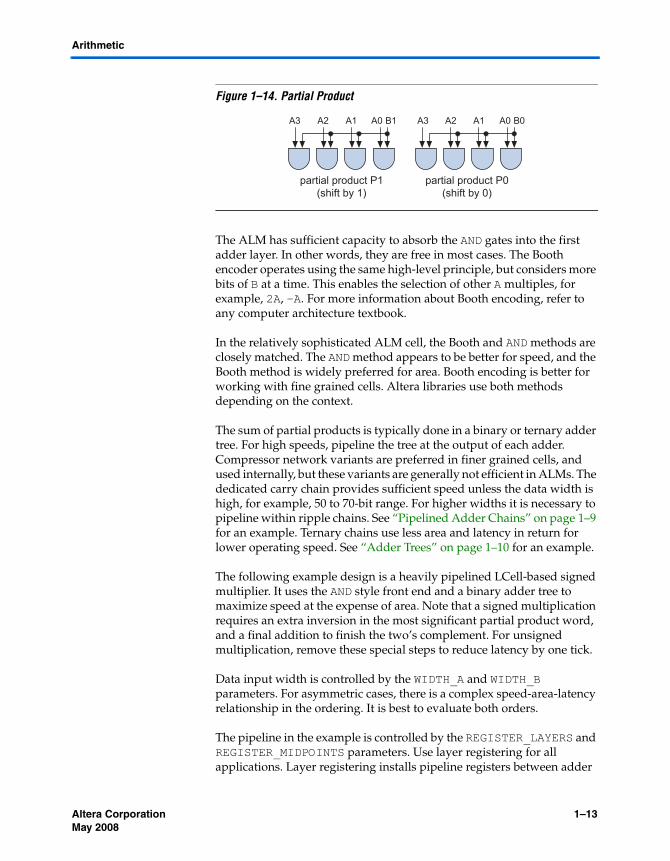
In the AND-based first stage each partial product is implemented as the A signal and one bit from the B signal. The partial product is A if B is one, and zero if B is zero. When shifted and summed, the result is the product (Figure 1–14).
*
A 2^B
Asign 0000
signed
A SHR N-B A SHL BA ASR N-B
A0000 0000
0
A ROL B
*
A 2^B
Table 1–1. Control Signals Used in Example File
Input Signal Name Value Value Value Value Value Value
shift_not_mult 0 1 1 1 1 1
direction_right x 1 1 0 1 0
shift_not_rot x 1 1 1 0 0
sign_a x 0 1 x x x
output(1) A * B(1) A shr B(1) A asr B(1) A shl B(1) A ror B(1) A rol B(1)
Table 1–1 note:(1) Output behavior is based on the input signal setting.
Example files: arithmetic/mult_shift.v (mult_shift_32_32 module)arithmetic/mult_shift_tb.v
Altera Corporation MegaCore Version a.b.c variable1–13May 2008
Arithmetic
Figure 1–14. Partial Product
The ALM has sufficient capacity to absorb the AND gates into the first adder layer. In other words, they are free in most cases. The Booth encoder operates using the same high-level principle, but considers more bits of B at a time. This enables the selection of other A multiples, for example, 2A, –A. For more information about Booth encoding, refer to any computer architecture textbook.
In the relatively sophisticated ALM cell, the Booth and AND methods are closely matched. The AND method appears to be better for speed, and the Booth method is widely preferred for area. Booth encoding is better for working with fine grained cells. Altera libraries use both methods depending on the context.
The sum of partial products is typically done in a binary or ternary adder tree. For high speeds, pipeline the tree at the output of each adder. Compressor network variants are preferred in finer grained cells, and used internally, but these variants are generally not efficient in ALMs. The dedicated carry chain provides sufficient speed unless the data width is high, for example, 50 to 70-bit range. For higher widths it is necessary to pipeline within ripple chains. See “Pipelined Adder Chains” on page 1–9 for an example. Ternary chains use less area and latency in return for lower operating speed. See “Adder Trees” on page 1–10 for an example.
The following example design is a heavily pipelined LCell-based signed multiplier. It uses the AND style front end and a binary adder tree to maximize speed at the expense of area. Note that a signed multiplication requires an extra inversion in the most significant partial product word, and a final addition to finish the two’s complement. For unsigned multiplication, remove these special steps to reduce latency by one tick.
Data input width is controlled by the WIDTH_A and WIDTH_B parameters. For asymmetric cases, there is a complex speed-area-latency relationship in the ordering. It is best to evaluate both orders.
The pipeline in the example is controlled by the REGISTER_LAYERS and REGISTER_MIDPOINTS parameters. Use layer registering for all applications. Layer registering installs pipeline registers between adder
A3 A2 A1 A0 B1 A3 A2 A1 A0 B0
partial product P1(shift by 1)
partial product P0(shift by 0)
1–14 MegaCore Version a.b.c variable Altera CorporationMay 2008
Multiplication of Large Integers (Karatsuba Algorithm)
layers, as well as partial product and output registers. For extreme speed, or high data widths, the midpoint setting installs an additional pipeline layer midway through each adder chain. Layer and midpoint latency numbers are logarithmic in the B width. The exact numbers are displayed in simulation as a convenience. For this 16 x 13 example, the layer latency is 6, and the additional midpoint latency is 4.
Note that the synthesis tools may infer RAM-based shift registers to implement some of the excess pipeline. The RAM is generally slower than cell registers. Setting the Quartus II Synthesis Optimization Technique to SPEED disables this inference, or you can explicitly disable this inference on a project or by entity using various settings.
Multiplication of Large Integers (Karatsuba Algorithm)
The Karatsuba multiplication algorithm is an efficient way to build high bit width integer multiplication, suitable for conserving DSP blocks in return for additional latency and cell area.
For example, when multiplying a pair of 64-bit numbers “A” and “B” consider the number split into 32-bit halves, {AH,AL} and {BH,BL}. The product is equivalent to (2**32 * AH + AL) * (2**32 * BH + BL). Multiplying through yields (2**64 * AH * BH) + (2**32 (AH*BL + AL*BH)) + (AL*BL). This is the familiar sum of four partial products structure.
The key of the Karatsuba algorithm is the observation that the middle term (2**32 (AH*BL + AL*BH)) is equivalent to 2**32 ((AH+AL) * (BH+BL) - (AH*BH) - (AL*BL)). AH*BH and AL*BL are already available. The remaining expression uses only one multiplier, allowing reformulation of the full product using only three product terms as shown in the following example:
pphh = AH*BH (64 bit)ppll = AL*BL (64 bit)pphl = (AH+AL)*(BH+BL) (66 bit)product = {pphh,ppll} + (pphl - pphh - ppll) << 32
This formulation requires additional add/subtract logic, and uses three rather than four multipliers. For high widths, you can recursively apply the algorithm to the partial product multipliers. Stratix II and Stratix III device families support extremely efficient DSP block multiplication up to 36 x 36 bits, making this is a good size for partial products. Adding numbers in the 64-bit range with adequate system speed requires some care. In particular, it requires considerable time to route from the DSP block output registers to adder inputs. To alleviate DSP routing pressure,
Example files: arithmetic/lc_mult_signed.varithmetic/lc_mult_signed_tb.v

Altera Corporation MegaCore Version a.b.c variable1–15May 2008
Arithmetic
the example file uses 3:2 compressors rather than carry chain adders to group the results. The final propagate adder is pipelined with latency two.
The partial product summation in the example file is optimized to exploit the shifting pattern of the inputs, as shown in Figure 1–15.
Figure 1–15. Shifting Pattern
In Figure 1–15, the product breaks into three distinct regions which are handled separately. The extra “ones” on the least significant end of the middle region complete the two’s complement negations (negative x = ~x + 1). The low order region is simply ppll[31:0] and requires no further work.
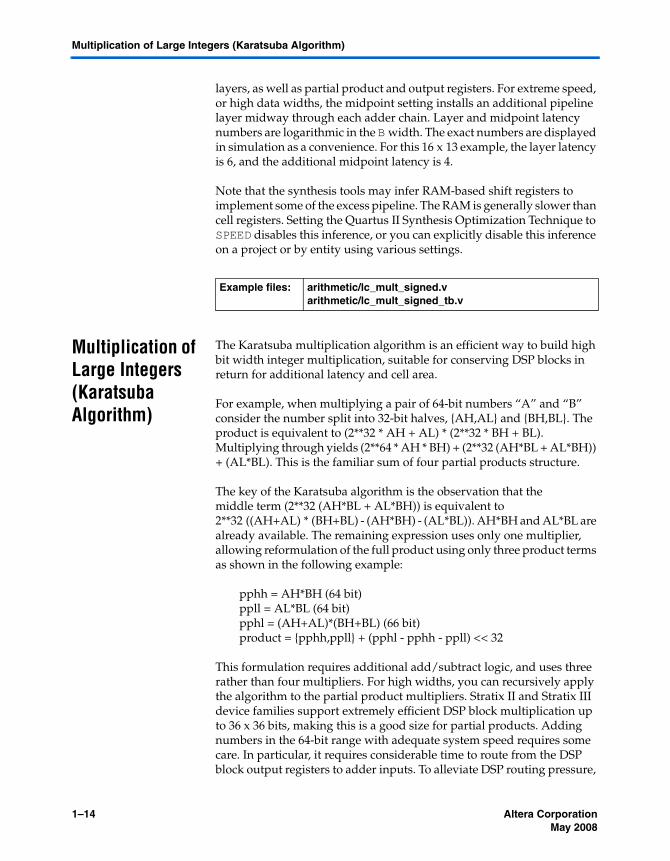
The first compressor array handles a part of the middle region of the product. The term pphl generates one clock cycle later and is not yet included in the pattern shown in Figure 1–15. Note that the +ones are deferred to make the implementation more efficient.
As shown in Figure 1–16 on page 1–16, the second compressor incorporates pphl and completes the deferred +one, and it is followed by a propagate adder to form the final sum. The final sum is positive and is equal to {pphh,ppll}[96:32] + AH*BL + AL*BH.
x127 x126 …x97 x96 x95 …x32 x31 x30 …x0
1 1 … 1 1 x’95 …x’32 1
1 1 … 1 1 x’95 …x’32 1
x97 x96 x95 …x32
31 bits 65 bits 32 bits
{pphh,ppll}
-pphh
-ppll
+pphl
1–16 MegaCore Version a.b.c variable Altera CorporationMay 2008
Multiplication of Large Integers (Karatsuba Algorithm)
Figure 1–16. Second Compressor
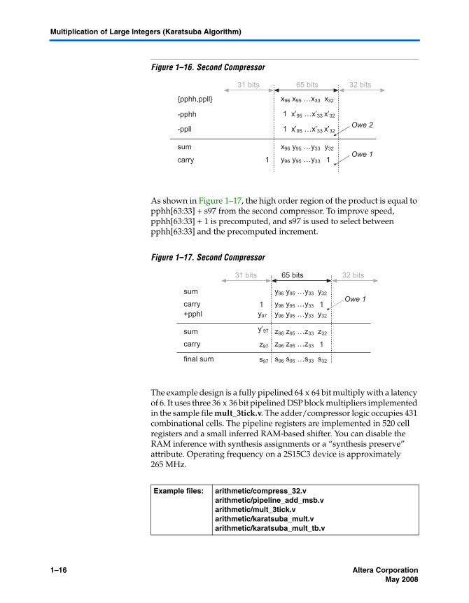
As shown in Figure 1–17, the high order region of the product is equal to pphh[63:33] + s97 from the second compressor. To improve speed, pphh[63:33] + 1 is precomputed, and s97 is used to select between pphh[63:33] and the precomputed increment.
Figure 1–17. Second Compressor
The example design is a fully pipelined 64 x 64 bit multiply with a latency of 6. It uses three 36 x 36 bit pipelined DSP block multipliers implemented in the sample file mult_3tick.v. The adder/compressor logic occupies 431 combinational cells. The pipeline registers are implemented in 520 cell registers and a small inferred RAM-based shifter. You can disable the RAM inference with synthesis assignments or a “synthesis preserve” attribute. Operating frequency on a 2S15C3 device is approximately 265 MHz.
Example files: arithmetic/compress_32.varithmetic/pipeline_add_msb.varithmetic/mult_3tick.varithmetic/karatsuba_mult.varithmetic/karatsuba_mult_tb.v
31 bits 65 bits 32 bits
{pphh,ppll}
-pphh
-ppll
sum
carry
x96 x95 …x33 x32
1 x’95 …x’33 x’32
1 x’95 …x’33 x’32
x96 y95 …y33 y32
y96 y95 …y33 1 1
Owe 2
Owe 1
31 bits 65 bits 32 bits
Owe 1sum y96 y95 …y33 y32
carry y96 y95 …y33 1 1
+pphl y97 y96 y95 …y33 y32
sum z96 z95 …z33 z32
carry z96 z95 …z33 z97 1
y’97
final sum s96 s95 …s33 s32 s97

Altera Corporation MegaCore Version a.b.c variable1–17May 2008
Arithmetic
Division (Unsigned Integer)
The lpm_divide megafunction implements a full division network with variable pipeline, producing one result per clock tick, but uses substantial area to do so. If N or N/2 ticks are available to operate on an N bit problem, then a much more efficient iterative algorithm is available.
Figure 1–18. Division
The circuit works using the elementary school algorithm of studying the numerator from left to right. When “difference“ is negative, the next quotient bit is 0 and “workspace“ is untouched. When “difference“ is zero or positive, the next quotient bit is set to one and “workspace“ is overwritten with the “difference“ value. The quotient bits accumulate in the “numerator“ register, and the remainder accumulates in the “workspace“ as the clock progresses. The “ready“ signal indicates completion in the example files (Figure 1–18).
It is possible to reduce the computation latency by studying more bits in parallel. For the radix-4 (two bits), case differences are computed for the denominator, 2*denominator, and 3*denominator using three parallel subtractors. Each tick decides the next two bits of quotient.
The example file and test bench file contain regular and radix-4 unsigned iterative dividers. For 32x32 bit data, the regular divider uses 154 ALUTs and operates at 257 MHz. The radix-4 uses 270 ALUTs and operates at 211 MHz.
Example files: arithmetic/divider.varithmetic/divider_tb.v
-
Circular shift
Division datpath
numeratorworkspace
denominator
difference

1–18 MegaCore Version a.b.c variable Altera CorporationMay 2008
Division (Unsigned Integer)
Altera Corporation MegaCore Version a.b.c variable 2–19May 2008
Chapter 2. FloatingPoint Tricks
Floating Point to Fixed Point Conversion
Single precision IEEE floating point numbers are stored in 32 bits in the following format:
bit 31 : sign bits 30:23 : exponentbits 22:0 mantissa
The equivalent value is 1.mantisa x 2**(exponent – 127).
1 Exceptional cases for dealing with infinity and denormalized numbers are not supported by these example files.
When operating in a tight range of numbers, convert to fixed point to reduce hardware cost. Fixed point numbers are viewed as integers multiplied by an unspoken power of 2. The exact power of two can be changed during calculation with bit shifting.
Moving from fixed to floating point requires scaling to obtain the implied leading 1. This is best accomplished with a modified barrel shifter. The barrel shifter must have a self-determined select which moves the data left until the most significant bit becomes a 1. The barrel shift method is demonstrated in the sample file scale_up.v. For more efficient iterative versions, use a linear or logarithmic shift register instead. For faster pipelined versions, embed registers between barrel shift layers. The hardware speed and cost are heavily dependent on the fixed point size.
Moving from floating to fixed point is more efficient because the shift distance can be computed directly from the float exponent.
Example file: float/scale_up.vfloat/fixed_to_float.vfloat/float_to_fixed.vfloat/fixed_to_float_tb.v (uses both example files)
2–20 MegaCore Version a.b.c variable Altera CorporationMay 2008
Approximate Square Root
Approximate Square Root
The computer graphics community has developed an impressive series of techniques for approximating floating point computations involving casting floating point numbers to 32-bit integers, then manipulating them directly.
The example file computes sqrt(x) using two adders and a shift. The adders have a large string of zeros on the less significant end, and the shifter is free. The resulting circuit cost is 17 ALUTs and has a provable maximum error of 6 percent.
Approximate Inverse Square Root
Computing 1 / (sqrt (x)) is quite useful for normalizing vectors. This example contains a very efficient first order approximation similar to the square root example. Additionally, it also has a parameter CORRECTION_ROUND, which adds a Newton refinement step.
This function is difficult to analyze in terms of error bound. For an engineering proof, the test bench evaluates 100,000 random x values. With the first order approximation, there are 64,891 values, which have an error of two to five percent. The rest have less than two percent error. When the correction round is enabled, all values have less than two percent error. Always confirm the results on the typical data range of your application.
With correction the circuit uses approximately 250 ALUTs and three 18x18 multipliers. The correction circuitry is fully pipelined with a latency of six. Without correction the circuit is one 32-bit subtractor.
The test bench uses a table of sample problems and error ranges loaded from the example file inv_sqrt.tbl. The C program was used to generate the table. It is included for experimenting with other data ranges.
Example files: float/approx_fp_sqrt.v float/approx_fp_sqrt_tb.v
Example file: float/approx_fp_inv_sqrt.v float/approx_fp_inv_sqrt_tb.v
Example file: float/test_stimulus.cppfloat/inv_sqrt.tbl

Altera Corporation MegaCore Version a.b.c variable 2–21May 2008
Floating Point Tricks
Approximate Floating Point Divide (Single Precision)
The IEEE single-precision floating-point divide function requires considerable logic area. The Altera floating-point divide megafunction uses approximately 1700 ALUTs and 845 memory bits for the default implementation. The example file demonstrates an approximation algorithm which allows 2% computational error in return for area reduction. This approximation requires 152 ALUT and one DSP multiplier block. It is fully pipelined with a latency of 5.
The quotient “A/B” is represented as the product of “A” and “1/B.” The “1/B” term is an approximation based on the most significant fraction bits of “B,” as shown in the following example:
E 1/B = 1 / (1.B[22]B[21]B[20]B[19]B[18]B[17] + 0.000001)where B = 1.B[22]B[21]…B[0]
The “E” computation is implemented as a 6-input 7-output look up implemented in the example file approx_fp_div_lut.v. The contents were generated with the small C program div_tbl_gen.cpp. “E” is always an underestimate of “1/B.” The exponent portion is computed directly by subtraction, and the multiplication is implemented in a fully pipelined DSP block as shown in example file mult_3tick.v. It is difficult to attain the fastest pipeline implementation with a generic “*” implementation.
Test bench simulation of this example requires a floating-point helper DLL. The DLL source files are in the utility directory. The build script is in the example file build_float_vpi.sh.
Example file: float/approx_fp_div.vfloat/approx_fp_div_lut.vfloat/approx_fp_div_tb.vfloat/mult_3tick.v

2–22 MegaCore Version a.b.c variable Altera CorporationMay 2008
Approximate Inverse Square Root

Altera Corporation MegaCore Version a.b.c variable 3–23May 2008
Chapter 3. Translation andFormat Conversion
One-Hot Decoder (Binary to One-Hot)
To convert a binary number to one-hot outputs, use single LUTs for up to 64 outputs (6 encoded inputs). Each LUT produces one output signal. For higher input counts, partition the input into 6-bit groups, then decode each group and merge the group with AND gates to create the final outputs.
The Quartus II Analysis and Synthesis automatically maps decoder structures in this way. Use the following simple formulation:
always @(in) beginout = 0;out[in] = 1'b1;
end
One-Hot to Binary
To convert an array of one-hot lines to binary, use an array of OR gates. Each OR gate reads half of the one-hot lines. The input pattern corresponds to the binary representation of the one-hot signal index: OR gate “0” reads every other input line, OR gate “1” reads alternate pairs, OR gate “2” reads alternate groups of four, and so on.
Example files: translation/one_hot.vtranslation/one_hot_tb.v
Example file: translation/onehot_to_bin.v

3–24 MegaCore Version a.b.c variable Altera CorporationMay 2008
Binary-to-Gray Conversion
Mask Generation
Generating binary bit masks for clipping data or masking RAM inputs is similar to implementation of one-hot decoding. Arbitrary functions of up to six inputs can be implemented in single LUTs per output bit by using a simple case statement as shown in the following example:
always @(in) begincase (in)
4'd0: mask=16'b1000000000000000;4'd1: mask=16'b1100000000000000;4'd2: mask=16'b1110000000000000;4'd3: mask=16'b1111000000000000;4'd4: mask=16'b1111100000000000;4'd5: mask=16'b1111110000000000;4'd6: mask=16'b1111111000000000;4'd7: mask=16'b1111111100000000;4'd8: mask=16'b1111111110000000;4'd9: mask=16'b1111111111000000;4'd10: mask=16'b1111111111100000;4'd11: mask=16'b1111111111110000;4'd12: mask=16'b1111111111111000;4'd13: mask=16'b1111111111111100;4'd14: mask=16'b1111111111111110;4'd15: mask=16'b1111111111111111;default: mask=0;
endcase
In this example, the extracted logic is 16 4-LUTs. Note that some minimization and factoring occurs. For example, the MSB is stuck at 1, and output bit 7 is equivalent to the most significant input bit. When the optimization technique value is set to SPEED, the resulting logic has depth of one. When using the default value BALANCED, the logic may be factored to improve area at the expense of depth.
The example files contain several variations of 16 and 32-bit masking, including the small C program used to generate the example files.
Binary-to-Gray Conversion
An efficient binary-to-gray conversion is implemented using an array of 2 input XOR gates. WIDTH -1 gates are required to convert a WIDTH bit value. Note that the output of the converter is not necessarily glitch-free and must be reregistered before passing across clock boundaries.
Example files: translation/mask_16.vtranslation/mask_32.vtranslation/make_mask.cpptranslation/mask_tb.v
Example file: translation/bin_to_gray.v

Altera Corporation MegaCore Version a.b.c variable 3–25May 2008
Translation and Format Conversion
Gray-To-Binary Conversion
Gray-to-binary conversion is less economical than binary-to-gray conversion (see “Binary-to-Gray Conversion” on page 3–24 for more information on binary-to-gray). The functionality of this conversion is essentially a chain of 2-input XOR gates with taps representing the binary outputs. To avoid deep propagation paths, the synthesis tool duplicates and flattens portions of the XOR chain, creating wider, shallower gates, implementing up to six bits in single LUTs. Beyond this width, the synthesis tool evaluates speed versus area, and makes trade-off determinations. This causes a certain amount of speed and area variability.
Seven Segment Display Driver
As with one-hot decoders, it is best to treat the seven segment display as a small ROM implemented in a case statement. The following example uses one 4-LUT for each of the 7 output bits. This pattern is dependent on all inputs for all output bits, so no additional minimization takes place.
case(bin)4'h0: seg = 7'b1000000; // out = 0 indicates lit4'h1: seg = 7'b1111001; // ---0---4'h2: seg = 7'b0100100; // | |4'h3: seg = 7'b0110000; // 5 14'h4: seg = 7'b0011001; // | |
4'h5: seg = 7'b0010010; // ---6---4'h6: seg = 7'b0000010; // | |4'h7: seg = 7'b1111000; // 4 24'h8: seg = 7'b0000000; // | |4'h9: seg = 7'b0011000; // ---3---4'ha: seg = 7'b0001000;4'hb: seg = 7'b0000011;4'hc: seg = 7'b1000110;4'hd: seg = 7'b0100001;4'he: seg = 7'b0000110;4'hf: seg = 7'b0001110;default : seg = 7'b1111111;
endcase
Example files: translation/bin_to_gray.vtranslation/gray_tb.v
Example file: translation/bin_to_7seg.v

3–26 MegaCore Version a.b.c variable Altera CorporationMay 2008
Binary-to-ASCII Hexadecimal Conversion
This example implements an 8-bit input rather than a 4-bit input. It approximates alphabetic letters stored in normal ASCII coding, and can be driven from Verilog HDL strings by using double quotation characters, as shown in the following example:
wire foo [15:0] = "ALTR";
1 Some of these approximations are incomplete alphabetic letters, but still useful for debugging.
Binary-to-ASCII Hexadecimal Conversion
Translating four bits of binary code to an ASCII hexadecimal byte requires two 3-LUTs and three 4-LUTs operating in parallel. In this translation, output bit 7 is stuck, and bits 4, 5, and 6 are derived from the same function.
The METHOD=0 version uses a readable compare/subtract function rather than proceeding directly to the LUT functions, causing some additional work for the synthesis tools. METHOD=1 is a case statement generated from METHOD=0 to make the expected implementation more obvious. This example accepts arbitrary length binary words, which are padded up to the appropriate 4-bit boundary.
ASCII Hexadecimal-to-Binary Conversion
This example translates an uppercase or lowercase ASCII hexadecimal byte to four bits. There are two versions controlled by the METHOD parameter:
■ METHOD=0—Invalid bytes must generate an output of 4'b0000. This version requires 15 ALUTs and depth two because all eight inputs must be examined by each output bit.
■ METHOD=1—This version simplifies the requirement to processing valid hex bytes, requiring four ALUTs and depth one. This illustrates the importance of careful default behavior selection.
Example file: translation/asc_to_7seg.v
Example file: translation/bin_to_asc_hex.v

Altera Corporation MegaCore Version a.b.c variable 3–27May 2008
Translation and Format Conversion
1 Replacing the default condition of METHOD=0 with 4'bxxxx creates a circuit between zero and one. Industrial CAD tools make local “greedy” decisions on “don’t care” assignment values due to a combination of infrequent occurrence, high analysis runtime, and generally disappointing returns. For best results, set “don’t-care” values by hand.
Binary-to-Decimal/Binary-Coded Decimal Adders
The example discussed in this section includes circuitry for converting 32-bit binary numbers to binary-coded decimal (BCD). For example, 4'hF becomes 16'h15. The patterns in the decimal representation of the powers of two cause interesting minimization opportunities. The most efficient method is compressing bit results followed by an adder tree, similar to the binary bit population count problem.
The adder tree needs modifications to carry at 10 rather than 16. The bcd_add_chain() module strings together 4-bit bcd_digit_add() modules to form a variable size BCD adder.
There are four versions of the digit adder controlled by the METHOD parameter:
■ METHOD=0—Case statement with “don’t cares.” This version does not minimize well because of the complexity of the ideal “don’t care” pattern.
■ METHOD=1—Adder variant.■ METHOD=2—Adder variant.■ METHOD=3—WYSIWYG cells based on METHOD=2. For most
applications, METHOD=3 is the best option.
The example file bin_to_dec.v implements a 32-bit to 10-decimal digit translation using the adder chain discussed above in conjunction with customized compressors. Each compressor takes 6 wires of the binary input and generates a BCD summation. The adder tree combines these summations to form the final output. This implementation uses 514 ALUTs which compares well to alternate structures. Note that this implementation is not high speed (approximately 14 ns of pin-to-pin delay on a 2S15C3 device). Additional registers may be required for satisfactory performance with high input data width.
Example file: translation/asc_hex_to_nybble.v
Example files: translation/bcd_add_chain.vtranslation/bin_to_dec.vtranslation/bin_to_dec_tb.v

3–28 MegaCore Version a.b.c variable Altera CorporationMay 2008
Binary-to-Decimal/Binary-Coded Decimal Adders

Altera Corporation MegaCore Version a.b.c variable 4–29May 2008
Chapter 4. Video
YCbCr (4:4:4) to RGB Conversion
The Y (luma) Cb (chroma blue) Cr (chroma red) format is a common intermediate format in digital video applications. The most common set of formulas takes Y with a nominal range of 16..235 and Cb and Cr in the 16..240 range. The RGB output range is from 0 to 255. Signals out of the range saturate to the appropriate values.
Use 9x9 fixed point multipliers in FPGA hardware design. The constants work out well to 9-bit signed numbers when scaled by 128 with the exception of the blue constant 2.017. Fortunately, the scaled value of 258 decomposes nicely into 2^8 (256) and 2^1 (2). The example file implements the majority of the terms in multipliers and decomposes the last blue term into a shift and add unit.
The test bench compares the result against a real number implementation. Note that errors can occur from the conversion to fixed point and truncation. The test bench requirement is that in over a million trials no 8-bit RGB term may deviate from the ideal result by more than +/–2. The test bench does allow inputs outside the nominal range. The error bar is smaller with realistic stimulus.
RGB to Hue Conversion
Hue is a color metric that is independent of lighting conditions. It is combined with lumience (L) and saturation (S) to form the HLS color system. The commonly used PC Paint program supports RGB as well as HLS in the color editing dialog for experimenting. Hue is typically stored as a number between 0 and 239. See Figure 4–2.
Figure 4–1. Color Arrangement
Example files: video/ycbcr_to_rgb.vvideo/ycbcr_to_rgb_tb.v
red 0
green 80 yellow 40
cyan 120
blue 160 magenta 200

4–30 MegaCore Version a.b.c variable Altera CorporationMay 2008
Sum of Absolute Difference (SAD)
The example design computes an 8-bit hue from 8-bit RGB values. It is designed around a ROM table of 4096 6-bit words. The 12-bit address limitation costs accuracy, but keeps the table within one 4K memory block. To recover accuracy when min (RGB) and max (RGB) are close, use the scaling stage in front of the table address lines. The test bench compares against the standard hue formula implemented with real numbers. In over 1 million trials no result deviates by more than +/–2 from the ideal value.
Sum of Absolute Difference (SAD)
Summing the difference of pixel values is a common step in video processing. It is the traditional bottleneck of MPEG4 encoding. Two pairs of 8-bit pixels can be compared efficiently in Stratix II hardware using two subtractors followed by a double addsub unit. Area cost is 27 arithmetic cells, using nine for each subtractor and nine for the double addsub chain.
Eight pair_sad units are combined with an adder tree to process a 4x4 array of pixels to make a typical MPEG-4 SAD unit. Area cost is 260 arithmetic mode cells (Figure 4–2).
Figure 4–2. Sum of Absolute Difference
Example files: video/rgb_to_hue.vvideo/rgb_to_hue_tb.v
Example file: arithmetic/pair_sad.v
Example file: arithmetic/fourbyfour_sad.v
Image A
SAD = abs(a0-b0) + abs (a1-b1) + ...+ abs (aF-bF)
Image B
b0
b4
b8
bC
b1
b5
b9
bD
b2
b6
bA
bE
b3
b7
bB
bF
a0
a4
a8
aC
a1
a5
aD
a2
a6
aA
aE
a3
a7
aB
aF
a9
Altera Corporation MegaCore Version a.b.c variable 4–31May 2008
Video
VGA Monitor Control
The most common pitfall when designing a VGA monitor controller is to completely abandon good synchronous design practices. The relatively low clock speed requirement tends to prompt unusual structures. Because of the predictable cycle behavior, it is easy to generate good registered outputs. Refraining from slow compare paths simplifies placement, leading to better results quality elsewhere in the design, and an advantage when moving to higher resolution modes.
The example uses a 27 MHz VGA clock and has parameter settings for the common 640x480 video mode. You can modify the timing parameters for other video modes. The appropriate timing (in microseconds) is available on numerous manufacturer websites. Divide by the desired clock period to convert from microseconds to clock ticks (1 microsecond is 10^–6 seconds, the reciprocal of the clock speed in Hz is the clock period in seconds). When experimenting with the hardware, older CRT displays are more tolerant of errors than newer LCDs. Most displays include the actual horizontal and vertical rates in the menu mode.
Example files: video/vga_driver.v

4–32 MegaCore Version a.b.c variable Altera CorporationMay 2008
VGA Monitor Control

Altera Corporation MegaCore Version a.b.c variable 5–33May 2008
Chapter 5. Arbitration
Bitscan (Priority Masking)
The bitscan function takes a set of request lines and allows only the least significant “1” to propagate. This function is handy for prioritizing interrupt request lines.
Figure 5–1. Bitscan Function
Arbiters with Fairness
Bus arbiters generally require a fairness scheme in addition to priority selection. The most common fairness scheme it to add a “next” signal which indicates a starting point for request consideration. For example, with request lines numbered 0..7 and “next” equal to 4, the request on line 4 is considered for a grant first, followed by 5..7, then by 0..3.
The example design implements an arbiter with a fairness index. The index must be delivered in one-hot format for this implementation. To accomplish this, generate it from a round-robin shift register. If this is not possible, it needs a one-hot decoder. The decoder method is illustrated in the test bench file arbiter_tb.v. The addition of the one-hot fairness index to a bitscan is an advanced technique that is smaller and faster than the more common shift-and-OR method.
Example file: arbitration/bitscan.varbitration/bitscan_tb.v
10001110010000
00000000010000
add
request -1
select
Example files: arbitration/arbiter.varbitration/arbiter_tb.v
5–34 MegaCore Version a.b.c variable Altera CorporationMay 2008
Priority Encoding
Priority Encoding
When a binary encoded output is desired from prioritized request lines, there are two reasonable methods. For smaller input counts, the best implementation is the case statement. A small C program is the best way to build these. The example file implements a 6-input priority encoder in exactly 3 LUTs using the case method.
For larger input sizes, the case statement method becomes infeasible. A reasonable alternative is to implement a bitscan function as described above followed by a one-hot to binary conversion array. An appropriate OR gate array is discussed in Chapter 3, Translation and Format Conversion, in “One-Hot to Binary” on page 3–23. An additional gate is required to deal with the all-lines-0 case.
Example files: arbitration/prio_encode.varbitration/prio_encode.cpp

Altera Corporation MegaCore Version a.b.c variable 6–35May 2008
Chapter 6. Multiplexing
Basic Multiplexing (Binary Encoded)
The Stratix II 6-LUT is perfectly suited for 4:1 multiplexer building blocks (4 data and 2 select inputs). The extended input mode facilitates implementing 8:1 blocks, and the fractured mode handles residual 2:1 multiplexer pairs (Figure 6–1).
Figure 6–1. 6-LUT
Express non-pipelined multiplexers in array notation as shown in the following example:
assign out = data [sel] ;
The Quartus II Synthesis automatically decomposes large multiplexers into suitable building blocks. More complex data arrangements can be implemented using case statements and generate loops. See “Decode/Select Multiplexing” on page 6–36.
Example file: muxing/simple_mux.v
6 LUT
d0d1d2d3
s0s1

6–36 MegaCore Version a.b.c variable Altera CorporationMay 2008
Basic Multiplexing (Binary Encoded)
Decode/Select Multiplexing
Decode/select multiplexing consists of decoding the select lines, using them to index data, and recombining the selected data (Figure 6–2).
Figure 6–2. Decode/Select Multiplexing
As a rule of thumb, LUT implementation of binary encoded multiplexers is more efficient than equivalent decode-select multiplexers. Synthesis tools generally identify decode-select pairs and convert them to encoded multiplexing logic. The notable exception is if the select signals already exist in one-hot form. This occurs frequently when the select lines are driven by a state machine.
The HDL case statement is interpreted as decode-select logic. The following code implements an 8-output one-hot decoder, and an 8-to-1 selector with several repeated data bits.
always @(sel or dat) begincase (sel)
3'd0: out = dat[0];3'd1: out = dat[1];3'd2: out = dat[3];3'd3: out = dat[2];3'd4: out = 1'b1;3'd5: out = 1'b0;3'd6: out = dat[0];3'd7: out = dat[1];default: out=0;
endcase
When using decode-select multiplexer logic, it is important to remember that the synthesis tool studies it closely for an encoded equivalent structure. Adding logic between the decoder and selector can cause recognition failures and reduced performance. For example, do not AND a chip select signal with the decoder output array. Instead, move the AND forward to the multiplexer output.
Data[8]Sel[3]
One-hotdecoder
Selector(one-hot multiplexer)
Altera Corporation MegaCore Version a.b.c variable 6–37May 2008
Multiplexing
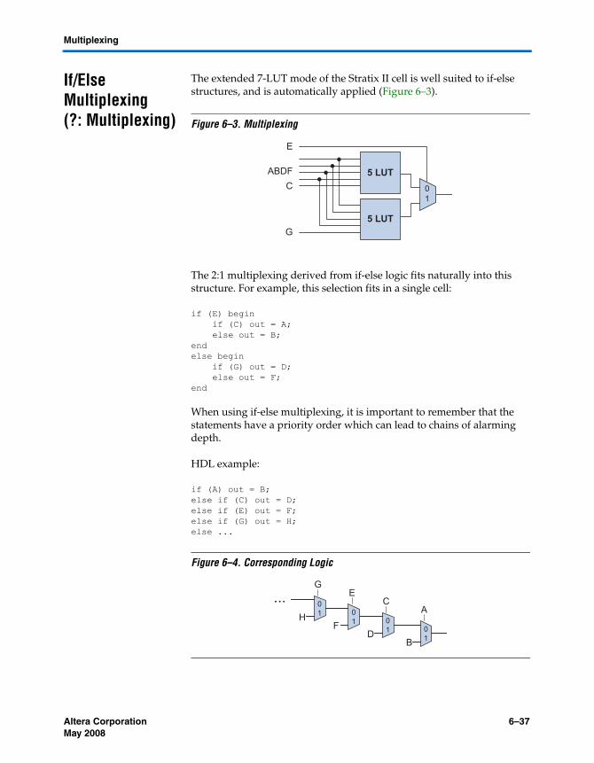
If/Else Multiplexing (?: Multiplexing)
The extended 7-LUT mode of the Stratix II cell is well suited to if-else structures, and is automatically applied (Figure 6–3).
Figure 6–3. Multiplexing
The 2:1 multiplexing derived from if-else logic fits naturally into this structure. For example, this selection fits in a single cell:
if (E) beginif (C) out = A;else out = B;
endelse begin
if (G) out = D;else out = F;
end
When using if-else multiplexing, it is important to remember that the statements have a priority order which can lead to chains of alarming depth.
HDL example:
if (A) out = B;else if (C) out = D;else if (E) out = F;else if (G) out = H;else ...
Figure 6–4. Corresponding Logic
E
C
G
ABDF 5 LUT
5 LUT
01
0
B
A0
D
C0
F
0
H
E…
01
01
01
01
G…
6–38 MegaCore Version a.b.c variable Altera CorporationMay 2008
Priority Multiplexing
The synthesis tools must assume that the select (A, C, E, G) signals require priority treatment, although this can be an artifact. If you are aware of the relationship of the select lines or repetition in the data lines, change the HDL to share more of this information with the CAD tool. This improves runtime and solution quality.
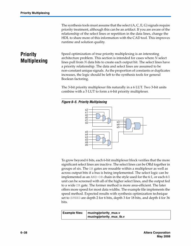
Priority Multiplexing
Speed optimization of true priority multiplexing is an interesting architecture problem. This section is intended for cases where N select lines pull from N data bits to create each output bit. The select lines have a priority relationship. The data and select lines are assumed to be non-constant unique signals. As the proportion of constants or duplicates increases, the logic should be left to the synthesis tools for general Boolean factoring.
The 3-bit priority multiplexer fits naturally in a 6 LUT. Two 3-bit units combine with a 5 LUT to form a 6-bit priority multiplexer.
Figure 6–5. Priority Multiplexing
To grow beyond 6 bits, each 6-bit multiplexer block verifies that the more significant select lines are inactive. The select lines can be ORd together in groups of six. The OR gates are reusable within a multiplexer as well as across output bits if a bus is being implemented. The select logic can be implemented as an AND-OR chain in the style used for the 6:1, or each 6:1 unit can be screened with all of the higher select lines, and the output fed to a wide OR gate. The former method is more area-efficient. The later offers more speed for most data widths. The example file implements the speed method. Expected results with synthesis optimization technique set to SPEED are depth 2 for 6 bits, depth 3 for 18 bits, and depth 4 for 36 bits.
Example files: muxing/priority_mux.vmuxing/priority_mux_tb.v
s4s5
s3
s2s1s0 d0
d2d1
s5s4s3d3
d5d4
Altera Corporation MegaCore Version a.b.c variable 6–39May 2008
Multiplexing
8-to-1 Multiplex Building Blocks
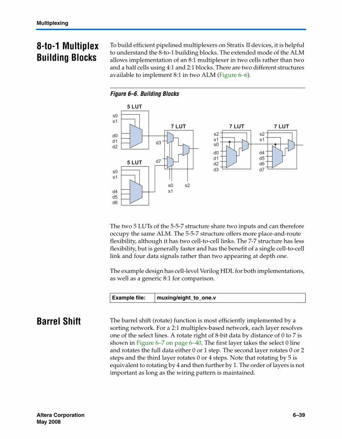
To build efficient pipelined multiplexers on Stratix II devices, it is helpful to understand the 8-to-1 building blocks. The extended mode of the ALM allows implementation of an 8:1 multiplexer in two cells rather than two and a half cells using 4:1 and 2:1 blocks. There are two different structures available to implement 8:1 in two ALM (Figure 6–6).
Figure 6–6. Building Blocks
The two 5 LUTs of the 5-5-7 structure share two inputs and can therefore occupy the same ALM. The 5-5-7 structure offers more place-and-route flexibility, although it has two cell-to-cell links. The 7-7 structure has less flexibility, but is generally faster and has the benefit of a single cell-to-cell link and four data signals rather than two appearing at depth one.
The example design has cell-level Verilog HDL for both implementations, as well as a generic 8:1 for comparison.
Barrel Shift The barrel shift (rotate) function is most efficiently implemented by a sorting network. For a 2:1 multiplex-based network, each layer resolves one of the select lines. A rotate right of 8-bit data by distance of 0 to 7 is shown in Figure 6–7 on page 6–40. The first layer takes the select 0 line and rotates the full data either 0 or 1 step. The second layer rotates 0 or 2 steps and the third layer rotates 0 or 4 steps. Note that rotating by 5 is equivalent to rotating by 4 and then further by 1. The order of layers is not important as long as the wiring pattern is maintained.
Example file: muxing/eight_to_one.v
5 LUT
d0d1d2
s0s1
5 LUT
d4d5d6
s0s1
7 LUT
d4d5d6d7
s2s1
7 LUT7 LUT
d0d1d2d3
s2s1s0
d7
s0s1
s2
d3
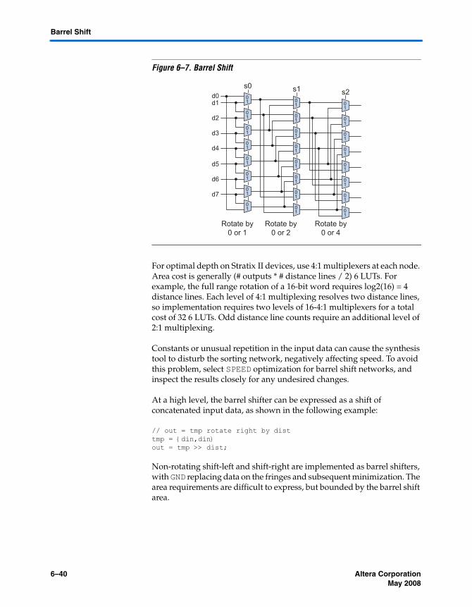
6–40 MegaCore Version a.b.c variable Altera CorporationMay 2008
Barrel Shift
Figure 6–7. Barrel Shift
For optimal depth on Stratix II devices, use 4:1 multiplexers at each node. Area cost is generally (# outputs * # distance lines / 2) 6 LUTs. For example, the full range rotation of a 16-bit word requires log2(16) = 4 distance lines. Each level of 4:1 multiplexing resolves two distance lines, so implementation requires two levels of 16-4:1 multiplexers for a total cost of 32 6 LUTs. Odd distance line counts require an additional level of 2:1 multiplexing.
Constants or unusual repetition in the input data can cause the synthesis tool to disturb the sorting network, negatively affecting speed. To avoid this problem, select SPEED optimization for barrel shift networks, and inspect the results closely for any undesired changes.
At a high level, the barrel shifter can be expressed as a shift of concatenated input data, as shown in the following example:
// out = tmp rotate right by disttmp = {din,din}out = tmp >> dist;
Non-rotating shift-left and shift-right are implemented as barrel shifters, with GND replacing data on the fringes and subsequent minimization. The area requirements are difficult to express, but bounded by the barrel shift area.
Rotate by0 or 1
Rotate by0 or 2
Rotate by0 or 4
d0d1
s0
d2
d3
d4
d5
d6
d7
01
01
01
01
01
01
01
01
s101
01
01
01
01
01
01
01
s201
01
01
01
01
01
01
01

Altera Corporation MegaCore Version a.b.c variable 6–41May 2008
Multiplexing
Building an explicit sorting network, as demonstrated in the example design, is necessary for custom pipelining. Additionally, it saves synthesis runtime for larger barrel systems, although it is not likely to change the final result.
Use of Register Secondary Signals for Multiplexing
The Stratix II register has built-in LAB-wide secondary signals that you can use to enhance pipelined multiplexing (Figure 6–8). The use of secondary signals introduces place-and-route restrictions, so inspect them carefully. The synthesis tools have built-in heuristics for analyzing routing impact, and infer secondary logic as appropriate. Always use caution when forcing secondary use through assignments or WYSIWYG. See Chapter 8, Registers and Memories, for more information.
Figure 6–8. Use of Stratix II Register Secondary Signals for Multiplexing
The synchronous load (SLOAD) signal is most applicable to multiplexer construction. It can be driven by a select line to implement an additional level of 2:1 multiplexing in a pipeline stage without using additional LUT logic. This is useful in barrel shifting contexts where the select line fan-out is naturally high.
Figure 6–9. Pipelined Sorting Networks
Example file: muxing/barrel_shift.v
aclrsclrsload
datain
clk
aload
regoutCLR
LD
D Q
DATAEN
adatasdata01
ena
S0,1 S2,3 S4,5
Sorting network is based on 4:1 multiplexer blocks, 6 lines resolved in latency three.
Sorting networkis based on 4:1 multiplexer blocks and SLOAD registers, 6 lines resolved in latency two.
S0,1 S3,4
SLOAD=S2SLOAD=S5
register
register
register
register
register
6–42 MegaCore Version a.b.c variable Altera CorporationMay 2008
Bus Multiplexing
Bus Multiplexing The ideal architecture for selecting between N independent K-bit words is an array of K N to 1 multiplexers. The structure can change a bit if the data words are repetitive. The synthesis tools can analyze repetition in the data and adapt accordingly. If certain data words are not needed, it is a good rule of thumb to connect the unused words to adjacent used data. The use of don’t care (X) can result in odd simulation behaviors. You can also use ground (000...) for unused data.
Bus multiplexers can be expressed concisely using two-dimensional array notation using System Verilog, but this practice is often unused due to historically inconsistent support. Instead, you can store data words concatenated together. The example file barrel_shift.v selects between words of concatenated data. For example, with data input {dog, cat, bear, fish}, and select = 2'b01, the “bear” data word is routed to the output.
Pipelined Bus Multiplexing
This example file pipelined_word_mux.v adds pipeline registers to the bus multiplexer structure. For high-speed operation in Stratix II devices, it is best to register between 4:1 multiplexer layers. This is controlled by the SELECTS_PER_LAYER parameter. The default setting is 2, and this setting corresponds to 2^2 or 4 to 1 multiplexers. You can also use a setting of 3 which uses 8:1 multiplexers. Pipelining after each 2:1 multiplexers works well in 4-LUT families, but tends to overuse routing in 6-LUTs. The data-to-output latency is:
(log base 2 (data words) / SELECTS_PER_LAYER)
The parameter BALANCE_SELECTS controls the select line latency. When the BALANCE_SELECTS parameter value is set to the default of 1, the design inserts additional registers to balance the select and data latency. In other words, the design is functionally equivalent to a multiplexer followed by output registers. With balancing turned off, the select line latency varies between a value of 1 and the maximum data latency. This feature can save some registers in cases where the control logic can handle the variable latency.
Example file: muxing/barrel_shift.v
Example file: muxing/pipelined_word_mux.vmuxing/pipelined_word_mux_tb.v
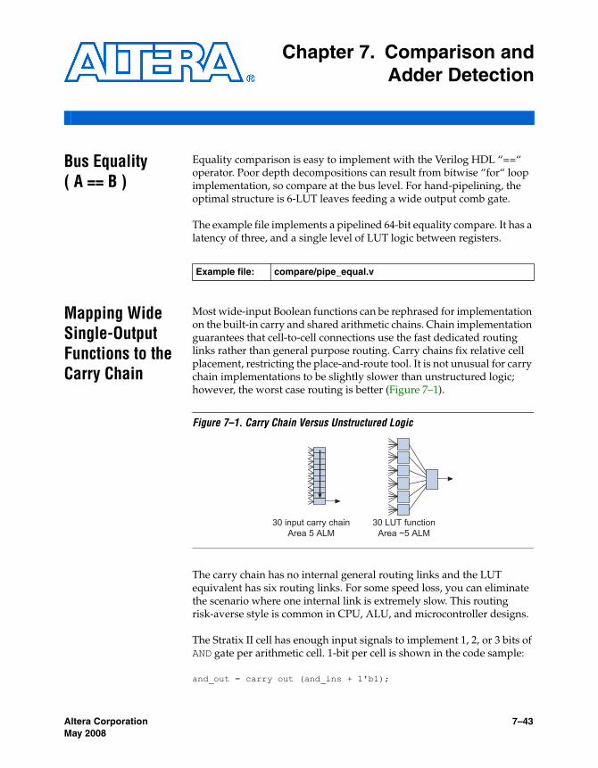
Altera Corporation MegaCore Version a.b.c variable 7–43May 2008
Chapter 7. Comparison andAdder Detection
Bus Equality ( A == B )
Equality comparison is easy to implement with the Verilog HDL “==“ operator. Poor depth decompositions can result from bitwise “for“ loop implementation, so compare at the bus level. For hand-pipelining, the optimal structure is 6-LUT leaves feeding a wide output comb gate.
The example file implements a pipelined 64-bit equality compare. It has a latency of three, and a single level of LUT logic between registers.
Mapping Wide Single-Output Functions to the Carry Chain
Most wide-input Boolean functions can be rephrased for implementation on the built-in carry and shared arithmetic chains. Chain implementation guarantees that cell-to-cell connections use the fast dedicated routing links rather than general purpose routing. Carry chains fix relative cell placement, restricting the place-and-route tool. It is not unusual for carry chain implementations to be slightly slower than unstructured logic; however, the worst case routing is better (Figure 7–1).
Figure 7–1. Carry Chain Versus Unstructured Logic
The carry chain has no internal general routing links and the LUT equivalent has six routing links. For some speed loss, you can eliminate the scenario where one internal link is extremely slow. This routing risk-averse style is common in CPU, ALU, and microcontroller designs.
The Stratix II cell has enough input signals to implement 1, 2, or 3 bits of AND gate per arithmetic cell. 1-bit per cell is shown in the code sample:
and_out = carry out (and_ins + 1'b1);
Example file: compare/pipe_equal.v
30 input carry chainArea 5 ALM
30 LUT functionArea ~5 ALM

7–44 MegaCore Version a.b.c variable Altera CorporationMay 2008
Equal to Constant
The addition carries out only when the and_ins constant is 1'b111...111. You can implement 2- or 3-bits per cell using the LUT in front of the adder to pre-AND pairs or triplets.
Table 7–1 lists the area and longest register-to-register delay for the carry_and.v example design surrounded by registers for various input widths.
Table 7–1 shows some falloff in the rate of speed improvement as the number of bits-per-cell increases due to increased routing difficulty. Essentially, the maximum density chain AND gate is slightly worse than the unstructured AND, however, the routing is guaranteed.
Other functions can be constructed by applying Demorgan’s theorem or manipulating the constant addition. It is not possible to obtain all wide functions in this manner due to the fixed carry backbone circuitry (for example, XORs).
Equal to Constant
Comparing a bus input to a constant value is a special case of the wide AND gate, where input signals associated with 0 bits are inverted. It maps efficiently to 6 LUTs with log base 6 (number of inputs) depth, and can be implemented using a carry chain AND gate for predictability, as shown in METHOD=1 of the example file.
Table 7–1. Register-to-Register Delay and Area for the carry_and.v Example
AND width Plain 1 Per Cell 2 Per Cell 3 Per Cell
16 1.153 ns 1.396 ns 1.242 ns 1.208 ns
5 comb 16 comb 8 comb 7 comb
32 1.483 ns 2.183 ns 1.546 ns 1.445 ns
9 comb 32 comb 16 comb 12 comb
64 1.900 ns 3.749 ns 2.464 ns 2.015 ns
19 comb 64 comb 32 comb 23 comb
128 2.418 ns 6.874 ns 4.033 ns 3.217 ns
37 comb 128 comb 64 comb 44 comb
Example file: compare/carry_and.v
Example file: compare/equal_const.v
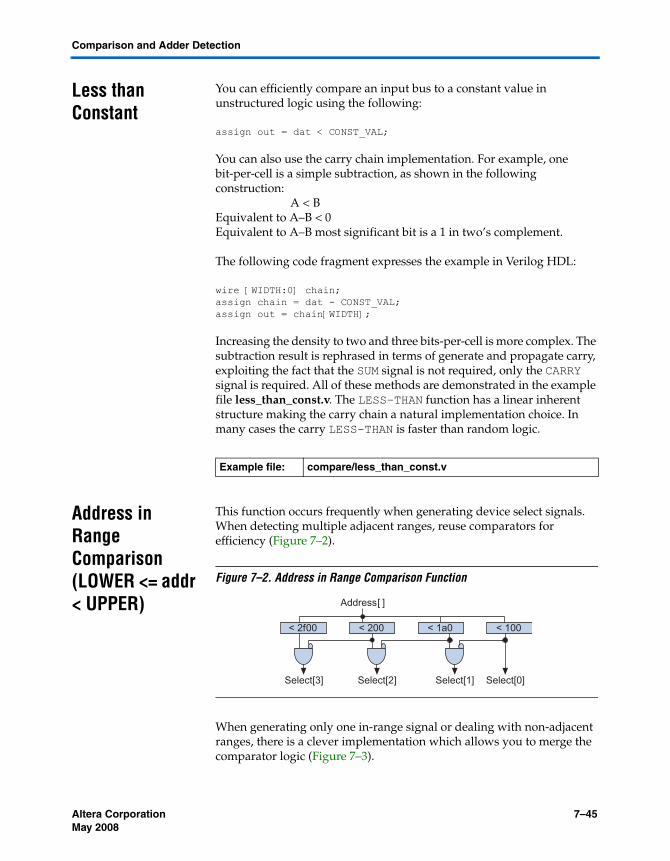
Altera Corporation MegaCore Version a.b.c variable 7–45May 2008
Comparison and Adder Detection
Less than Constant
You can efficiently compare an input bus to a constant value in unstructured logic using the following:
assign out = dat < CONST_VAL;
You can also use the carry chain implementation. For example, one bit-per-cell is a simple subtraction, as shown in the following construction:
A < BEquivalent to A–B < 0Equivalent to A–B most significant bit is a 1 in two’s complement.
The following code fragment expresses the example in Verilog HDL:
wire [WIDTH:0] chain;assign chain = dat - CONST_VAL;assign out = chain[WIDTH];
Increasing the density to two and three bits-per-cell is more complex. The subtraction result is rephrased in terms of generate and propagate carry, exploiting the fact that the SUM signal is not required, only the CARRY signal is required. All of these methods are demonstrated in the example file less_than_const.v. The LESS–THAN function has a linear inherent structure making the carry chain a natural implementation choice. In many cases the carry LESS-THAN is faster than random logic.
Address in Range Comparison (LOWER <= addr < UPPER)
This function occurs frequently when generating device select signals. When detecting multiple adjacent ranges, reuse comparators for efficiency (Figure 7–2).
Figure 7–2. Address in Range Comparison Function
When generating only one in-range signal or dealing with non-adjacent ranges, there is a clever implementation which allows you to merge the comparator logic (Figure 7–3).
Example file: compare/less_than_const.v
< 100< 1a0< 200
Address[ ]
Select[0]Select[1]Select[2]Select[3]
< 2f00
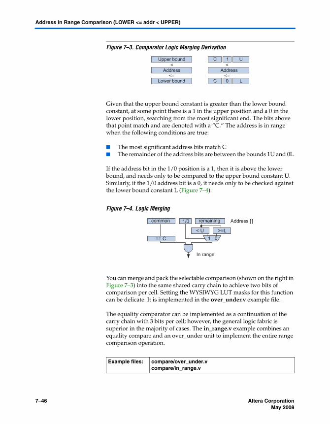
7–46 MegaCore Version a.b.c variable Altera CorporationMay 2008
Address in Range Comparison (LOWER <= addr < UPPER)
Figure 7–3. Comparator Logic Merging Derivation
Given that the upper bound constant is greater than the lower bound constant, at some point there is a 1 in the upper position and a 0 in the lower position, searching from the most significant end. The bits above that point match and are denoted with a “C.“ The address is in range when the following conditions are true:
■ The most significant address bits match C■ The remainder of the address bits are between the bounds 1U and 0L
If the address bit in the 1/0 position is a 1, then it is above the lower bound, and needs only to be compared to the upper bound constant U. Similarly, if the 1/0 address bit is a 0, it needs only to be checked against the lower bound constant L (Figure 7–4).
Figure 7–4. Logic Merging
You can merge and pack the selectable comparison (shown on the right in Figure 7–3) into the same shared carry chain to achieve two bits of comparison per cell. Setting the WYSIWYG LUT masks for this function can be delicate. It is implemented in the over_under.v example file.
The equality comparator can be implemented as a continuation of the carry chain with 3 bits per cell; however, the general logic fabric is superior in the majority of cases. The in_range.v example combines an equality compare and an over_under unit to implement the entire range comparison operation.
Example files: compare/over_under.vcompare/in_range.v
Upper bound
Address
Lower bound
<
<=
C
Address
C
<
<=
1
0
U
L
>=L
common 1/0
< U
remaining
1 0
In range
Address [ ]
== C

Altera Corporation MegaCore Version a.b.c variable 7–47May 2008
Comparison and Adder Detection
Match or Inverse Match
Note that this function is a generalized version of the Ethernet FCS error detect with “stomping.” To determine if binary words are matching or opposite, you can use the following function, however, do not use this directly in Verilog HDL:
(bus_a == bus_b) || (bus_a == ~bus_b)
There is an efficient 6 LUT structure that reuses the leaf nodes to implement both halves of the comparison simultaneously. It is roughly half the size of the traditional dual comparator, and in most cases faster (Figure 7–5 on page 7–47).
Figure 7–5. Matching
Decompose the problem recursively into 3-bit sub problems implemented in 6-LUTs. The rightmost LUT in Figure 7–5 compares bits 2..0 from the A and B busses. Its output is a 1 when the 3-bit signals are equal or opposite, for example, A=“110“ and B=“110,“ or A = “101“ and B = “010.“ Additional comparisons are necessary to verify that the clusters of three agree on the sense of the match. The leftmost LUT in Figure 7–5 operates on one bit from each sub problem to verify that the other LUTs are in agreement on matching, or in agreement on inverted matching, and not a mixture. You can extend the structure to arbitrary bus width. The maximum depth grows slowly (log base 6) with the width of the output AND gate.
Example file: compare/match_or_inv.v
eq || op
a b
eq || op
a b
eq || op
a b
eq || op…Extend todesired width

7–48 MegaCore Version a.b.c variable Altera CorporationMay 2008
Match or Inverse Match
Min and Max / Variable Sign Comparison
Generating the min and max of two numbers (min = (a<b) ? a : b) is required in many video processing contexts. The circuit requires a “less than“ comparator and an array of 2:1 multiplexers for each output bus. Min- or max-only variants are common in Viterbi implementations.
Comparison with a dynamic signed/unsigned control is surprisingly efficient. The sign control is used only when comparing the most significant bit pair of the data. There are two reasonable implementations of the comparator: flattened logic and carry chain. For Stratix II devices, the flattened logic is generally more efficient. There are also two reasonable implementations of the 2:1 mulitplexer array: 3-LUT and register SLOAD MUX. The SLOAD MUX results in area savings, and the 3-LUT variant produces higher clock speeds. The example design uses a random logic comparator and has parameter control for the multiplexer.
The modules min_max_signed and min_max_unsigned are generic fixed sign units provided for testing. The module min_max_8bit is a hand-factored variable sign version designed for video. To change the data width, you must extend the comparator.
Example files: compare/min_max.vcompare/min_max_tb.v
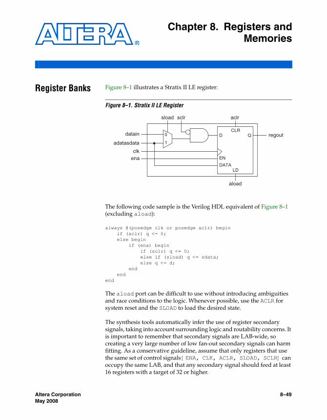
Altera Corporation MegaCore Version a.b.c variable 8–49May 2008
Chapter 8. Registers andMemories
Register Banks Figure 8–1 illustrates a Stratix II LE register:
Figure 8–1. Stratix II LE Register
The following code sample is the Verilog HDL equivalent of Figure 8–1 (excluding aload):
always @(posedge clk or posedge aclr) beginif (aclr) q <= 0;else begin
if (ena) beginif (sclr) q <= 0;else if (sload) q <= sdata;else q <= d;
endend
end
The aload port can be difficult to use without introducing ambiguities and race conditions to the logic. Whenever possible, use the ACLR for system reset and the SLOAD to load the desired state.
The synthesis tools automatically infer the use of register secondary signals, taking into account surrounding logic and routability concerns. It is important to remember that secondary signals are LAB-wide, so creating a very large number of low fan-out secondary signals can harm fitting. As a conservative guideline, assume that only registers that use the same set of control signals [ENA, CLK, ACLR, SLOAD, SCLR] can occupy the same LAB, and that any secondary signal should feed at least 16 registers with a target of 32 or higher.
aclrsclrsload
datain
clk
aload
regoutCLR
LD
QD
DATAEN
adatasdata0
1
ena

8–50 MegaCore Version a.b.c variable Altera CorporationMay 2008
24-Bit/16-Bit Stream Buffers (RGB/Memory Buffer)
Cautions aside, the register bank is an excellent construct for dictating secondary signals: there is guaranteed minimum fan-out and closely related functionality. The common functionality and use as a block tends to draw the bits together during place-and-route. If place-and-route benefits from having the registers together, then the secondary signals become added information.
24-Bit/16-Bit Stream Buffers (RGB/Memory Buffer)
This example converts a 24-bit input stream to a 16-bit stream, and back. The original application moved an RGB video stream through a word oriented RAM buffer. This is a good example of complex shift register behavior, and you do not have to go through the difficult process of figuring out the necessary states on paper.
The storage shift registers are the bulk of the area cost; 73 ALUTs for the 2 to 3-byte case, and 91 ALUTs for the 3 to 2-byte side. In general, the control logic mapping is determined by the synthesis tool. The Quartus II software, version 6.1 and later, takes advantage of the SCLR parameter for the rst signal, and some SLOAD and ENABLE. These can fluctuate if the acknowledge and valid signals are driven by external gates.
RAM-Based Shift Register
Use RAM blocks to implement larger shift registers. The Quartus II Synthesis infers RAM-based shift registers (altshift_taps) automatically. There are restrictions on the number and placement of output taps. RAM shift registers are most efficient when taps are evenly spaced and widely separated.
You can build a simple delay line-type shift register by hand. The example file ram_delay_reg.v implements a 7-tick 64-bit delay line. Latency two accounts for the RAM input and output register layers. RAM blocks are stitched together automatically to satisfy the size requirements, and the DEPTH parameter should be greater than two.
Example file: register/register_bank.v
Example files: register/buf_3to2.vregister/buf_2to3.vregister/buffer_tb.v
Example files: register/ram_delay_reg.vregister/ram_delay_reg_tb.v

Altera Corporation MegaCore Version a.b.c variable 8–51May 2008
Registers and Memories
FIFO (Dual Clock)
Dual clock FIFO is a notoriously temperamental building block. This implementation is provided for users who want to gain understanding or get a head start on a special purpose modification. For typical use, you can use the dcfifo megafunction in the Quartus II software.
The central issue to compare the read and write address pointers across unrelated clock domains. The FIFO system must always elect the more conservative response when data is incompletely transferred. The standard solution is to cross domains using gray-coded pointers (Figure 8–2 on page 8–51).
Figure 8–2. Gray-Coded Pointers
When properly arranged, the gray-coded signals ensure that a clock collision results in the use of the older pointer value. For example, if the read and write pointers are both at address 7, the FIFO is empty and read is not allowed. When a write arrives, the write pointer advances to 8. For this example, suppose a write occurs a very short time before the next read clock edge. The write pointers update reliably, but the read side observes the write pointers during transition. The binary encoded write address switches from “0111” to “1000.” All of the bits change, and the read side can observe any possible value. The arbitrary value would cause havoc with the “used words” and “read empty” decisions. Gray coding defeats this scenario; the gray-coded write address switches from “0100” to “1100.” The MSB may still not capture properly, but the others will capture properly. This limits the possible outcomes to the old value of 7 and the new value of 8, both of which are acceptable in terms of functionality.
For some high-reliability applications, you may want to enhance the clock crossing logic. Some aerospace applications execute the clock domain crossing in triplicate and use a majority circuit on the recovery side. In most cases, the additional circuitry simply reduces latency. In the previous example, a majority circuit increases the probability that the fresh write became available immediately, rather than one read clock cycle later. Additional clock crossing logic or synchronizer registers also
Read Pointer Simple Dual PortRAM
Gray Code
Gray Code
Read Domain
Write Domain
Write Pointer
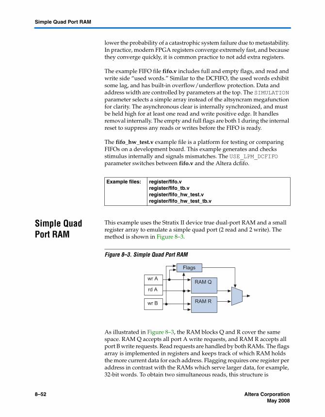
8–52 MegaCore Version a.b.c variable Altera CorporationMay 2008
Simple Quad Port RAM
lower the probability of a catastrophic system failure due to metastability. In practice, modern FPGA registers converge extremely fast, and because they converge quickly, it is common practice to not add extra registers.
The example FIFO file fifo.v includes full and empty flags, and read and write side “used words.” Similar to the DCFIFO, the used words exhibit some lag, and has built-in overflow/underflow protection. Data and address width are controlled by parameters at the top. The SIMULATION parameter selects a simple array instead of the altsyncram megafunction for clarity. The asynchronous clear is internally synchronized, and must be held high for at least one read and write positive edge. It handles removal internally. The empty and full flags are both 1 during the internal reset to suppress any reads or writes before the FIFO is ready.
The fifo_hw_test.v example file is a platform for testing or comparing FIFOs on a development board. This example generates and checks stimulus internally and signals mismatches. The USE_LPM_DCFIFO parameter switches between fifo.v and the Altera dcfifo.
Simple Quad Port RAM
This example uses the Stratix II device true dual-port RAM and a small register array to emulate a simple quad port (2 read and 2 write). The method is shown in Figure 8–3.
Figure 8–3. Simple Quad Port RAM
As illustrated in Figure 8–3, the RAM blocks Q and R cover the same space. RAM Q accepts all port A write requests, and RAM R accepts all port B write requests. Read requests are handled by both RAMs. The flags array is implemented in registers and keeps track of which RAM holds the more current data for each address. Flagging requires one register per address in contrast with the RAMs which serve larger data, for example, 32-bit words. To obtain two simultaneous reads, this structure is
Example files: register/fifo.vregister/fifo_tb.vregister/fifo_hw_test.vregister/fifo_hw_test_tb.v
RAM Q
RAM R
Flags
wr A
rd A
wr B

Altera Corporation MegaCore Version a.b.c variable 8–53May 2008
Registers and Memories
duplicated. The flag storage array is reused. This type of simple quad RAM is attractive for CPU-style register files. For 32 words of 32 bits, the area required is approximately 160 ALUTs and 4 Kilobits (Kb) of memory. The circuit operates at the speed and latency of the normal RAM block.
Ternary Content Addressable Memory (TCAM)
Content Addressable Memory (CAM) refers to RAM that is addressable by data rather than address. Ternary CAM (TCAM) means that the data may contain “don’t care” bits. CAM is analogous to a hash table.
The most common FPGA application is the storage of routing tables. An address comes into the table and is directed to one or more output links based on a subset of the address bits (Figure 8–4).
Figure 8–4. Grouping Ternary Adders
Some older Altera FPGA devices contain programmable pterm arrays suitable for CAM. However, for newer device families, CAM must be implemented using register arrays or standard RAM. Binary CAM implementation using standard RAM is straight forward; the role of address and data are reversed. However, as the data width increases, this method is no longer feasible; 32-bit data would require 4 billion addressable words. Some form of external stitching is necessary to control memory use. Ternary CAM is more challenging to build because the “don’t care” requirement necessitates additional logic or encoding. Techniques to solve this problem based on available resources are shown in the example file.
Example files: register/simple_quad.vregister/register/simple_quad_tb.vregister/flag_array.v
0a.ee.33.44
27.xx.xx.xx
27.01.xx.xx
Where is27.01.ab.03?
here
here

8–54 MegaCore Version a.b.c variable Altera CorporationMay 2008
Ternary Content Addressable Memory (TCAM)
Register-Based Ternary CAM
Register-based CAM is similar to a traditional register file on the write side. Each storage word has a data mask and a “don’t care” mask. The traditional read multiplexer is replaced with an array of ternary comparators. Figure 8–5 illustrates a single storage word. It is equivalent to the reg_cam_cell.v example file.
Variable sized register-based CAMs are easy to construct by changing the register file parameters. Memory bit efficiency is high, and access time is low. The example file reg_cam_cell.v has single tick read and write access. The area cost in registers is considerable as shown by the sample benchmark numbers in Table 8–1. This method is only suitable for small CAMs where write access time is important.
Figure 8–5. Variable Sized Register-Based CAMs
Table 8–1 lists the register file parameters used in the example file reg_cam_cell.v.
Table 8–1. Register File Parameters
Bits Words Registers fMAX (MHz 2S15C3)
32 16 1173 296
64 16 2293 271
96 16 3413 235
128 16 4533 227
32 64 4391 232
32 128 8680 206
Example files: register/reg_cam_cell.vregister/reg_based_cam.vregister/reg_based_cam_tb.v
Data bits
Don’t Care bits
Ternarycomparator
Lookup dataWrite data
matchDecoded writeaddr

Altera Corporation MegaCore Version a.b.c variable 8–55May 2008
Registers and Memories
RAM-Based Ternary CAM
The main issue in building CAM from standard RAM is how to handle “don’t care.” The ideal RAM would be a RAM that uses different read and write access patterns, as shown in Figure 8–6 on page 8–55.
Figure 8–6. Variable Sized Register-Based CAMs
For example, when writing data 01x to address 2, you can write the entire address = 2 column, checking the 010 and 011 bits (as shown in Figure 8–6), and clearing the other bits. Then, for lookup access, read the entire data row to generate address match lines. Unfortunately, the FPGA RAM blocks are not arranged for asymmetric read write patterns. The example design approximates the column write with a small state machine that writes each location in turn.
For Stratix II device 4Kbit memory blocks, the best configuration for this application is 128 words. 128 is the maximum number of words you can use at the maximum hardware output width of 36. Only 32 of the outputs are connected in the example file to create a power of two. You can remove this restriction in return for some additional stitching complexity. The example file cam_ram_block.v implements a RAM-based CAM building block with 128 words (7 data bits) and a 5-bit address. Lookups are fully pipelined at the RAM latency of 2, and writes use the state machine to iterate through the 128 storage words. Therefore, write latency is 128 ticks plus 2 to initiate the cycle. Note that it is not possible to pipeline writes. The example file ram_based_cam.v demonstrates stitching the blocks horizontally to build wider data.
Increasing address space beyond 32 words can be done directly in the ADDR_WIDTH parameter through the altsyncram megafunction. This underlying megafunction builds wider data words by stitching RAMs together, increasing the size of the match logic. You can also manually stitch together the blocks by partitioning the address space. To do so, you can use the highest order address bits to select between independent CAMs. If the write latency of 128 is too high, but 64 or 32 is acceptable, reduce the data width of the building block. This results in lower RAM efficiency because the maximum output width does not increase beyond
XData 000Data 001Data 002
X X
…A
ddr 0A
ddr 1A
ddr 2A
ddr 3A
ddr 4A
ddr 5A
ddr 6

8–56 MegaCore Version a.b.c variable Altera CorporationMay 2008
Ternary Content Addressable Memory (TCAM)
36 bits. An alternate solution is to provide more intelligent “don’t care” support. It may not be necessary to review all 128 data words for all writes.
Multiple stitched CAM blocks may use identical state machines. By default, the Quartus II software recognizes this duplication and merges the blocks appropriately. For high-speed implementations, you can maintain the duplicate blocks using hierarchical synthesis or a /*synthesis preserve*/ attribute. This allows the driving logic to stay physically close to the memory blocks.
Example file: register/ram_block.vregister/cam_ram_block.vregister/ram_based_cam.vregister/ram_based_cam_tb.v

Altera Corporation MegaCore Version a.b.c variable 9–57May 2008
Chapter 9. Counters
Basic Binary Counter
The following Verilog HDL example implements a basic binary “up” counter with the full set of register secondary signals:
always @(posedge clk or posedge rst) beginif (rst) q <= 0;
else beginif (ena) begin
if (sclear) q <= 0;else if (sload) q <= sdata;else q <= q + 1'b1;
endend
end
The area cost is one ALUT per bit (two per ALM). The LUT logic in front of the dedicated adder remains available for special control signals including enable, direction, or varying increments.
Up/Down Counter
When enhancing a counter with additional controls, it is advantageous to express them in terms of the inputs to the addition rather than multiplexing the adder output. The following example illustrates the best manner in which to express up/down control:
q <= q + (inc_not_dec ? 1'b1 : {WIDTH{1'b1}});
This structure mirrors the available LUT hardware, establishing the one cell per bit intention explicitly. The synthesis tools can recognize a wide variety of output side logic and move this logic to the input side, but there remains some risk of an unintentional increase in area.
Example file: counter/cntr.v
Example file: counter/cntr_updn.v

9–58 MegaCore Version a.b.c variable Altera CorporationMay 2008
Modulus Counter with Lookahead
Seconds Timer This example implements a stopwatch timer based on a 100 MHz reference clock. The straight forward implementation as a 27 bit modulus counter has a few drawbacks. Foremost, a 27-bit carry chain and output comparator require significant propagation time. Although it is acceptable to run at 100 MHz, it is safer to add some pipeline to simplify timing closure. Additionally, it is likely that future revisions will require more output precision. Any expansion is likely to be decimal rather than binary oriented. For example, hundredths of a second would be more useful than 1/128ths.
This implementation separates the counter into two divide-by 1000 stages and a divide-by 100 stage. This separation breaks up the propagation path and puts the internal storage in decimal format, with negligible additional area cost. It is important to avoid the temptation to ripple the clock between stages. The clock ripple may be advantageous for power consumption, but creates routing and timing analysis problems on the FPGA. Most CAD tools issue warnings when riple clocking is used.
The “tick” output pin pulses high for one clock cycle every second. The count_val register indicates the elapsed time in seconds from the last reset. Note that the internal register div_three is hundredths of a second. If you are modifying the counters for a different grouping or reference frequency, the lowest counter needs to compare against the maximum value minus 1 (998), while the others compare the maximum (999 or 99) to maintain the proper look-ahead behavior.
Modulus Counter with Lookahead
Due to the relatively high cost of a modulus computation for arbitrary constants, you may want to use the maximum value comparison, as shown in the following example:
wire maxed = (q == MOD_VAL-1) /* synthesis keep */;always @(posedge clk or posedge rst) begin
if (rst) q <= 0;else begin
if (ena) beginif (sclear) q <= 0;else if (sload) q <= sdata;else q <= (maxed ? 0 : q) + (maxed ? 0 : 1'b1);
endend
end
Example file: counter/seconds_counter.vcounter/seconds_counter_tb.v
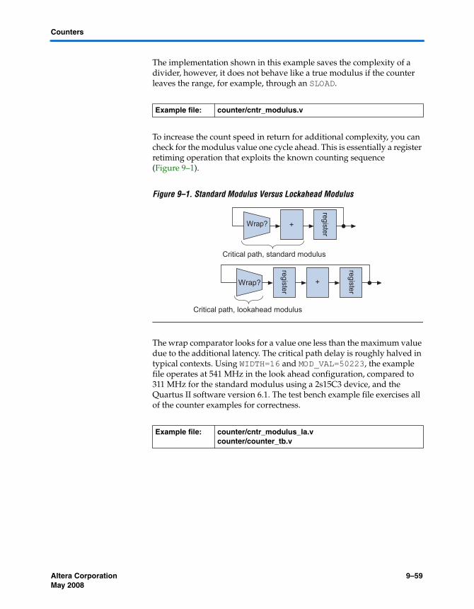
Altera Corporation MegaCore Version a.b.c variable 9–59May 2008
Counters
The implementation shown in this example saves the complexity of a divider, however, it does not behave like a true modulus if the counter leaves the range, for example, through an SLOAD.
To increase the count speed in return for additional complexity, you can check for the modulus value one cycle ahead. This is essentially a register retiming operation that exploits the known counting sequence (Figure 9–1).
Figure 9–1. Standard Modulus Versus Lockahead Modulus
The wrap comparator looks for a value one less than the maximum value due to the additional latency. The critical path delay is roughly halved in typical contexts. Using WIDTH=16 and MOD_VAL=50223, the example file operates at 541 MHz in the look ahead configuration, compared to 311 MHz for the standard modulus using a 2s15C3 device, and the Quartus II software version 6.1. The test bench example file exercises all of the counter examples for correctness.
Example file: counter/cntr_modulus.v
Example file: counter/cntr_modulus_la.vcounter/counter_tb.v
+ regWrap?
+ regWrap? reg
Critical path, lookahead modulus
+
register
Wrap?
+Wrap?
Critical path, standard modulus
register
register

9–60 MegaCore Version a.b.c variable Altera CorporationMay 2008
Modulus Counter with Lookahead
Basic Gray Counter and Gray Lookahead
Incrementing a gray-coded number can be awkward. There are several reasonable implementations; the most straightforward method is to build a binary counter followed by a binary-to-gray converter (see Chapter 3, Translation and Format Conversion for more information). Because the underlying state is not gray, the outputs must be reregistered to be glitch free. To count directly in gray, use the logic structure shown in Figure 9–2.
Figure 9–2. Logic Structure
The example design gray_cntr.v implements the structure shown in Figure 9–2. The conversions and increment are implemented in simple combinational logic to encourage the synthesis tools to flatten through. For widths up to 6 bits, the logic fits into single cells. If you are using higher widths, you may encounter significant propagation time. For best depth, use the optimize=speed setting in the Quartus II Integrated Synthesis.
At the cost of additional code complexity, you can build faster gray counters using the lookahead technique as described in “Seconds Timer” on page 9–58. The example design that follows can implement width 5 to 35 counters, with a single level of logic between registers.
Example file: counter/gray_cntr.v
Gry to bin +1 Bin to gry DFF

Altera Corporation MegaCore Version a.b.c variable 9–61May 2008
Counters
The counter width is decomposed into blocks of five registers, implemented in the gray_cntr_la_reg module. The MSB depends on six input signals for one level of logic. The adv_lower and adv_upper signals control the increment pattern. The LSB toggles on every other cycle, and the MSBs toggle when the bits below them hold the pattern 100... in binary.
always @(*) begind[0] = q[0] ^ adv_lower;d[1] = q[1] ^ (adv_upper & q[0]);d[2] = q[2] ^ (adv_upper & !q[0] & q[1]);d[3] = q[3] ^ (adv_upper & !q[0] & !q[1] & q[2]);d[4] = q[4] ^ (adv_upper & !q[0] & !q[1] & !q[2] & q[3]);
end
Figure 9–3 on page 9–61 shows a sample counting pattern.
Figure 9–3. Counting Pattern
The least significant block of five bits does a straightforward alternation between lower and upper increments. The more significant blocks use registered comparators from the lower blocks to compute advance signals. Each block has a registered comparator for the maximum (10000) and minimum (00000) value. The blocks use these to generate advance signals for following blocks, adv_lower[] and adv_upper[]. The lowest block also generates an “early“ version of the advance upper signal so that subsequent signals can use an extra cycle of latency to maintain depth 1.
Example files: counter/gray_cntr_la.vcounter/gray_cntr_tb.v
Sample counting pattern:
0
0
0
0
1
0
0
0
1
1
0
0
0
1
0
0
0
1
1
0
1
1
1
0
1
0
1
0
0
0
1
0
0
0
1
1
1
0
1
1
1
1
1
1
0
1
1
1
0
1
0
1
1
1
0
1
1
0
0
1
0
0
0
1

9–62 MegaCore Version a.b.c variable Altera CorporationMay 2008
Modulus Counter with Lookahead
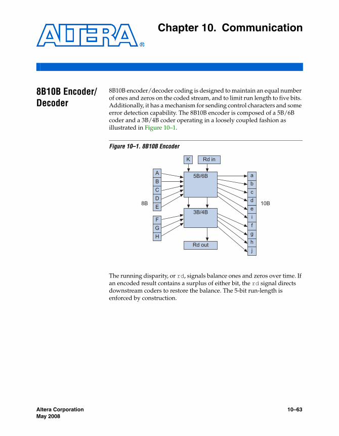
Altera Corporation MegaCore Version a.b.c variable 10–63May 2008
Chapter 10. Communication
8B10B Encoder/ Decoder
8B10B encoder/decoder coding is designed to maintain an equal number of ones and zeros on the coded stream, and to limit run length to five bits. Additionally, it has a mechanism for sending control characters and some error detection capability. The 8B10B encoder is composed of a 5B/6B coder and a 3B/4B coder operating in a loosely coupled fashion as illustrated in Figure 10–1.
Figure 10–1. 8B10B Encoder
The running disparity, or rd, signals balance ones and zeros over time. If an encoded result contains a surplus of either bit, the rd signal directs downstream coders to restore the balance. The 5-bit run-length is enforced by construction.
ABCDE
abcdeifghj
FGH
8B 10B
5B/6B
3B/4B
Rd out
Rd inK

10–64 MegaCore Version a.b.c variable Altera CorporationMay 2008
8B10B Encoder/ Decoder
The K signal is used to transmit control characters. Only some of the 8-bit inputs represent legal control characters. K28.5 is the standard link synchronization or idle character, although K28.7 and K28.1 are also suitable.
The following list shows the legal K control characters:
K28.0 8'b000_11100K28.1 8'b001_11100K28.2 8'b010_11100K28.3 8'b011_11100K28.4 8'b100_11100K28.5 8'b101_11100 (comma)K28.6 8'b110_11100K28.7 8'b111_11100K23.7 8'b111_10111K27.7 8'b111_11011K29.7 8'b111_11101K30.7 8'b111_11110
Decoding is essentially the reverse of the encoding lookup. It is unnecessary to know the running disparity to recover the data, which simplifies the process. The example decoder file decoder_8b10b.v has optional logic to detect disparity errors and general coding errors.
In terms of synthesis behavior, these example designs are a fascinating case study for speed optimization. The original paper that introduced 8B10B contains a carefully optimized version for implementation in 2- and 3-input MECL logic gates. To some extent, this structure has propagated to the modern HDL descriptions. The high reuse of duplicate signals, coupled with intentionally redundant expressions, makes the logic very misleading to modern FPGA synthesis tools. The typical result is a sub-optimal depth of four due to overuse of common sub expressions. The optimizations in the example files work by removing some of the gate structure using case tables, and by recreating the most difficult signals as WYSIWYG gates.
The example encoder has a maximum depth of two levels and uses 56 ALUTs. The decoder has a maximum depth of two levels on all paths except the kerr output which is depth three, using 42 ALUTs with both error check outputs enabled.
Example file: communication/encoder_8b10b.vcommunication/decoder_8b10b.vcommunication/encoder_tb.v

Altera Corporation MegaCore Version a.b.c variable 10–65May 2008
Communication
Universal Asynchronous Receiver Transmitter (UART)
The universal asynchronous receiver transmitter (UART) provides a simple and efficient mechanism for communicating with a host PC. For example, a basic UART implementing the 115200 baud N81 protocol costs only 62 ALUTs. The example design file uart.v implements a variable baud N81 UART. Because other protocols are rarely used, they are not included in the example file, however, you can implement these protocols by modifying the TX and RX shift registers. The example transmitter can operate up to the system fMAX of approximately 420 MHz. The receiver requires over sampling to recover data reliably, with the theoretical receive speed limit of roughly 84 million baud. Because PC COM ports and typical RS232 cables are incapable of 84 million baud, 115200 baud is the practical PC port limit. Some special purpose PC expansion cards are reaching into the five to ten million range, approaching standard cable limits.
On the host end, you can communicate with a COM port using Hyper Terminal, found in Accessories on Windows, or any similar terminal emulation program. You must disable the flow control, also referred to as XON/XOFF. For automated interfacing, a COM port can be opened as a file from C. The method to set the data rates and timeouts is platform-specific and may require some research.
The example design uart_hw_test implements a simple demo for use with a terminal app. It takes input characters on the receive side and sends the following character (for example, “a” –> “b”) out the transmitter.
Example file: communication/uart.vcommunication/uart_tb.vcommunication/uart_hw_test.v

10–66 MegaCore Version a.b.c variable Altera CorporationMay 2008
Universal Asynchronous Receiver Transmitter (UART)

Altera Corporation MegaCore Version a.b.c variable 11–67May 2008
Chapter 11. CyclicRedundancy Check
Introduction Cyclic redundancy checks (CRCs) in FPGAs are generally unrolled to operate on multiple data bits per cycle, and implemented as wide XOR arrays. The Stratix II 6-LUT has a strong advantage over 4-LUT devices when implementing CRC XORs with shallow depth.
1 32 bit CRCs with a specific bit ordering are referred to as Frame Check Sequences (FCS) in network context. See “CRC-32 Ethernet FCS” on page 11–70.
Figure 11–1. Cyclic Redundancy Check
The following code example illustrates unrolled HDL showing XORs for a CRC8 of 4-bit data:
assign crc_out[0] = c[4] ^ d[3];assign crc_out[1] = c[4] ^ c[5] ^ d[2] ^ d[3];assign crc_out[2] = c[4] ^ c[5] ^ c[6] ^ d[1] ^ d[2] ^ d[3];assign crc_out[3] = c[5] ^ c[6] ^ c[7] ^ d[0] ^ d[1] ^ d[2];assign crc_out[4] = c[0] ^ c[6] ^ c[7] ^ d[0] ^ d[1];assign crc_out[5] = c[1] ^ c[7] ^ d[0];assign crc_out[6] = c[2];assign crc_out[7] = c[3];
Due to XOR input cancellation, the intermediate stages of a CRC bit computation do not resemble the final output, giving rise to a common implementation pitfall.
C2C3C5 C4 C1 C0
Data bit
N bit shift register. Polynomial is represented by feedback points
+
+
+
+
D7
D6
Unrolled for multiple data bits
C2 C2C3 C0

11–68 MegaCore Version a.b.c variable Altera CorporationMay 2008
CRC XOR Decomposition
Figure 11–2. CRC Implementation Pitfalls
The two structures shown in Figure 11–2 are logically equivalent, however, the bottom structure is considerably faster. Each 8-data unit has a natural depth of two cells for a total of eight logic levels. The 32-data unit can also be implemented with a depth of two. When dealing with variable width input data, for example, packet residues, the fastest results are obtained by implementing a separate XOR network for each data input width and multiplexing the output. CRC XOR arrays are relatively efficient in terms of area, and due to cancellation, the area cost increases very slowly with data width. The area premium paid for parallel speed is easily manageable in practice.
Figure 11–3. CRC XOR Arrays
CRC XOR Decomposition
The CRCs in the example file use explicitly factored XOR trees to minimize Stratix II cell area while maintaining optimum depth. They use the WYSIWYG XOR cell in the example file to make the structure completely explicit. You can override the METHOD parameter to produce equivalent flat XORs. This switch is intended for comparison and testing rather than actual implementation.
CRC328 data
CRC328 data
CRC328 data
CRC328 data
CRC3232 data
CRC3216 dat
CRC3232 dat
MultiplexerMode
Data/CRC
Example file: crc/xor6.v

Altera Corporation MegaCore Version a.b.c variable 11–69May 2008
Cyclic Redundancy Check
CRC-16 Fixed Data Width
The example files use the standard 16-bit CRC polynomial 1021 (hexadecimal), and are all depth optimal at two levels. Area cost ranges from 17 to 53 ALUT.
CRC-32 Fixed Data Width
The following example files use the standard 32-bit CRC hexadecimal polynomial 04c11db7, and are all depth optimal; at two levels for 8..32, and at three levels for 40..64 bits. Area cost ranges 42 from 205 ALUT.
The following example files extend the data range up to 128 bits, and are all depth optimal at 3 levels, with area cost ranging from 205 to 507 ALUT.
CRC-32 Variable Data Width (Residues)
The example file crc32_dat64_any_byte.v computes the CRC-32 of one to eight bytes of data, as is required to handle packet residues. Typically, the various width data inputs are driven from different subsets of the same 64-bit register, but there is no additional cost to drive them from different sources, even though generally different sources cost more.
There are two reasonable implementations of the 8:1 output multiplexer (see “8-to-1 Multiplex Building Blocks” on page 6–39 in Chapter 6, Multiplexing). The 7-7 method allows the design to have a maximum LUT depth of four, with the four deeper CRC units feeding the output
Example files: crc/crc16_dat8.vcrc/crc16_dat16.vcrc/crc16_dat24.vcrc/crc16_dat32.v
Example files: crc/crc32_dat8.vcrc/crc32_dat16.vcrc/crc32_dat24.vcrc/crc32_dat32.vcrc/crc32_dat40.vcrc/crc32_dat48.vcrc/crc32_dat56.vcrc/crc32_dat64.v
Example files: crc/crc32_dat72.vcrc/crc32_dat80.vcrc/crc32_dat88.vcrc/crc32_dat96.vcrc/crc32_dat104.vcrc/crc32_dat112.vcrc/crc32_dat120.vcrc/crc32_dat128.v

11–70 MegaCore Version a.b.c variable Altera CorporationMay 2008
CRC-32 Ethernet FCS
side cell. The 5-5-7 method produces a depth five implementation, which is in return more routable. Both methods require roughly 1100 ALUTs. The multiplexing format selection is left to the synthesis tool in this example.
The example files contain 4-byte (32-bit) and 16-byte (128-bit) variants. The 4-byte unit has a maximum LUT depth of three, and uses roughly 375 ALUTs. It is also used in the Ethernet example file crc_ethernet.v (see “CRC-32 Ethernet FCS”). The 16-byte unit has maximum LUT depth of five, and uses roughly 4143 ALUTs.
The crc32_tb.v example file contains a test bench showing the proper transitivity of the 32- and 64-byte variable units. The crc32_128_tb.v example file contains further exercise of the 128 any byte unit.
CRC-32 Ethernet FCS
The example file implements a 1..4 byte parallel CRC-32 unit, a register bank, and the bit order shuffling you typically use in Ethernet:
■ The CRC output bits are reversed and inverted. ■ The CRC register is synchronously initialized to 32'hffffffff using the
init signal■ Data residues appear on the less significant end of the data bus.■ The LSB of the most significant byte enters the calculation first.
The test bench at the bottom of the example file demonstrates the popular “123456789” test to help resolve any confusion.
Example file: crc/crc32_dat64_any_byte.v
Example files: crc/crc32_dat32_any_byte.vcrc/crc32_dat128_any_byte.v
Example file: crc/crc32_tb.vcrc/crc32_128_tb.v
Example files: crc/crc_ethernet.vcrc/crc_register.v

Altera Corporation MegaCore Version a.b.c variable 12–71May 2008
Chapter 12. Error CorrectionCodes
64/72-Bit ECC Encoder/ Decoder
The most common RAM error correction scheme uses eight additional parity bits per 64 bits of data. This is sufficient for the correction of any single bit error, and detection of two bit errors. The eight parity bits form a 7-bit Hamming code, and an additional parity bit that is used to distinguish between single and double errors.
The decoder recomputes the parity of the data and compares against the saved parity bits. For a correct code word, the result is all zeros. An incorrect code word generates the index of the bad bit, referred to as the syndrome. This scheme is applicable to any data width.
The examples shown in Figures 12–1 through 12–3 use 7-bit data with four parity bits to illustrate this process. For further reading, see the Wikipedia entry for Mr. Hamming and “hamming matrix.”
Figure 12–1 shows an encoding example.
Figure 12–1. Encoding Example
Notes to Figure 12–1:(1) 7-bit data is interleaved with parity bits to form an 11-bit code word. The parity bits
are generated by XORs of data bits in an alternating pattern.
Figure 12–2 shows a decoding example with no errors.
0 1 1
0 1 1 1 10 0
0 1 0 0 1 1 1 1
++
+
+

12–72 MegaCore Version a.b.c variable Altera CorporationMay 2008
64/72-Bit ECC Encoder/ Decoder
Figure 12–2. Decoding Example With no Errors
Notes to Figure 12–2:(1) The recomputed parity bits, XORed with the code parity, is all 0s indicating no
correction is necessary. The second layer decoder circuitry does not toggle any bits.
Figure 12–3 shows a decoding example with an error.
Figure 12–3. Decoding Example With an Error
Notes to Figure 12–3:(1) The non-zero parity value indicates the position of the error in the code word. In
this case, 1001, or decimal nine, indicates the ninth of 11 bits is incorrect. The non-zero decoder output is XORed with the data to produce the correct output despite the corruption.
The additional parity bit is needed to distinguish between single- and double-bit errors. Any single error changes the parity of the data. 2-bit errors are recognized because they have non-zero decoded parity, but no change in the extra parity bit. Typically, higher error counts are misinterpreted as single or double errors.
0 1 1 1 1010110
0 0 1 0 0010110
++
1 1 0 0 110
0000
+
+
++ + ++ + +decoder
1 1 0 0 110
1001
+
0 0 1 0 1011010
0 1 1 1 1010010
decoder+ + + + + + +
++
+
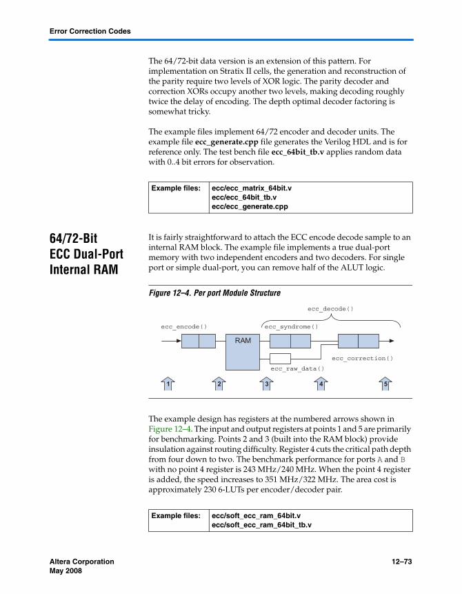
Altera Corporation MegaCore Version a.b.c variable 12–73May 2008
Error Correction Codes
The 64/72-bit data version is an extension of this pattern. For implementation on Stratix II cells, the generation and reconstruction of the parity require two levels of XOR logic. The parity decoder and correction XORs occupy another two levels, making decoding roughly twice the delay of encoding. The depth optimal decoder factoring is somewhat tricky.
The example files implement 64/72 encoder and decoder units. The example file ecc_generate.cpp file generates the Verilog HDL and is for reference only. The test bench file ecc_64bit_tb.v applies random data with 0..4 bit errors for observation.
64/72-Bit ECC Dual-Port Internal RAM
It is fairly straightforward to attach the ECC encode decode sample to an internal RAM block. The example file implements a true dual-port memory with two independent encoders and two decoders. For single port or simple dual-port, you can remove half of the ALUT logic.
Figure 12–4. Per port Module Structure
The example design has registers at the numbered arrows shown in Figure 12–4. The input and output registers at points 1 and 5 are primarily for benchmarking. Points 2 and 3 (built into the RAM block) provide insulation against routing difficulty. Register 4 cuts the critical path depth from four down to two. The benchmark performance for ports A and B with no point 4 register is 243 MHz/240 MHz. When the point 4 register is added, the speed increases to 351 MHz/322 MHz. The area cost is approximately 230 6-LUTs per encoder/decoder pair.
Example files: ecc/ecc_matrix_64bit.vecc/ecc_64bit_tb.vecc/ecc_generate.cpp
Example files: ecc/soft_ecc_ram_64bit.vecc/soft_ecc_ram_64bit_tb.v
RAM
ecc_encode() ecc_syndrome()
ecc_correction()
ecc_raw_data()
ecc_decode()
21 3 4 5
12–74 MegaCore Version a.b.c variable Altera CorporationMay 2008
ECC 32/39-Bit Variation
1 The two RAM ports do not operate at exactly the same speed due to differences in the allowable modes multiplexing. You can use this test design for observing the discrepancy without the ECC logic; it varies depending on the RAM mode settings.
ECC 32/39-Bit Variation
To correct 32-bit data, 39 bits of RAM storage is required. The encoder uses 38 ALUTs with two levels of logic. The decoder is 132 ALUTs and depth five without the point 4 register. The soft RAM depth profile is similar to that of the 64/72 variant, however, the logic is easier to place-and-route, and it can operate at 382 MHz/387 MHz (with register point 4 enabled).
ECC 16/22-Bit Variation
To correct 16-bit data, 22 bits of RAM storage is required. The RAM example file soft_ecc_ram_16bit.v uses approximately 89 ALUT per encode/decode pair, and operates at 424 MHz/435 MHz.
ECC 8/13-Bit Variation
To correct 8-bit data, 13 bits of RAM storage is required. The encoding requires one level of logic. Decoding uses three levels of logic with optimization “technique equals speed.” By default, the point 4 register in the decoder is disabled due to the lower depth. The area cost is approximately 32 ALUT per encoder/decoder pair, operating at approximately 443 MHz/445 MHz.
Example file: ecc/ram_speed_test.v
Example files: ecc/ecc_matrix_32bit.vecc/ecc_32bit_tb.vecc/soft_ecc_ram_32bit.vecc/soft_ecc_ram_32bit_tb.v
Example files: ecc/ecc_matrix_16bit.vecc/ecc_16bit_tb.vecc/soft_ecc_ram_16bit.vecc/soft_ecc_ram_16bit_tb.v
Example files: ecc/ecc_matrix_8bit.vecc/ecc_8bit_tb.vecc/soft_ecc_ram_8bit.vecc/soft_ecc_ram_8bit_tb.v

Altera Corporation MegaCore Version a.b.c variable 12–75May 2008
Error Correction Codes
ECC 2/6-Bit Variation
This example file corrects 2-bit data using 6-bit codes. Encoding is simple, consisting of two 2-input XOR gates. Decoding uses two 6-LUTs for data, and three 6-LUTs for error flagging (0, 1, or more errors).
The C program file ecc_2bit.cpp generates the Verilog HDL and is included for reference only. The test bench checks all of the 0-, 1-, and 2-bit error scenarios.
Reed-Solomon Forward Error Correction (FEC)
Reed-Solomon error correction is a widely used method for protecting larger data streams. The Digital Video Broadcast (DVB) standard represents a typical set of parameters. 255 symbols of 8 bits each are used to transmit 239 bytes of data. The 16 check symbols are sufficient to correct up to eight bad symbols, and to detect up to 16 bad symbols. The latency is usually 1 tick per symbol (255 for DVB), in contrast with the typical RAM ECC schemes. Smaller Reed-Solomon codes are used on audio CD-ROMs. The operation is based on fairly complicated Galois field arithmetic.
For more information on Reed-Solomon hardware, see the BBC White Paper (July 2002), “WHP 031: Reed-Solomon error correction,“ by C.K.P Clarke. The paper contains a digest version of the underlying Galois mathematics. For more discussion of the underlying theory, go to www.mathworld.wolfram.com, or another pure math website.
1 Altera offers a Reed-Solomon MegaCore IP which has more features than the example file, including variable code sizes, sophisticated bus flow control signals, and some throughput/area tradeoff variants. Additionally, this IP core has decoder support for erasures.
Reed-Solomon Transmitter
The Reed-Solomon transmit side is relatively straightforward. It consists of a parity generator and a simple state machine to alternately send data and parity symbols. The parity generator resembles a CRC unit (Figure 12–5 on page 12–76).
Example files: ecc/ecc_2bit.vecc/ecc_2bit_tb.vecc/ecc_2bit.cpp
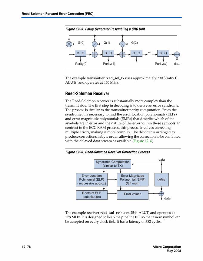
12–76 MegaCore Version a.b.c variable Altera CorporationMay 2008
Reed-Solomon Forward Error Correction (FEC)
Figure 12–5. Parity Generator Resembling a CRC Unit
The example transmitter reed_sol_tx uses approximately 230 Stratix II ALUTs, and operates at 440 MHz.
Reed-Solomon Receiver
The Reed-Solomon receiver is substantially more complex than the transmit side. The first step in decoding is to derive an error syndrome. The process is similar to the transmitter parity computation. From the syndrome it is necessary to find the error location polynomials (ELPs) and error magnitude polynomials (EMPs) that describe which of the symbols are in error and the nature of the error within these symbols. In contrast to the ECC RAM process, this process involves correcting multiple errors, making it more complex. The decoder is arranged to produce corrections in byte order, allowing the correction to be combined with the delayed data stream as available (Figure 12–6).
Figure 12–6. Reed-Solomon Receiver Correction Process
The example receiver reed_sol_rx() uses 2544 ALUT, and operates at 178 MHz. It is designed to keep the pipeline full so that a new symbol can be accepted on every clock tick. It has a latency of 382 cycles.
D Q D Q
data
…
Parity(n)
G(0) G(1) G(2)
Parity(0) Parity(1)
D Q D Q
data
delay
data
Syndrome Computation(similar to TX)
Error LocationPolynomial (ELP)
(successive approx)
Error MagnitudePolynomial (EMP)
(GF mult)
Roots of ELP(substitution)
Error values

Altera Corporation MegaCore Version a.b.c variable 12–77May 2008
Error Correction Codes
w The decoder “failure” signal (too many errors to correct) is not implemented. It should be configured to check that the degree of the ELP is less than or equal to T (in this case, eight). In some cases, you may also need to configure it to check that the number of roots identified matches the degree.
Table 12–1 lists the contents of the Reed-Solomon example files.
Example files: ecc/reed_sol.vecc/reed_sol.cpp
Table 12–1. Reed-Solomon example file contents (Part 1 of 2)
File Name/ Generator Contents Description
reed_sol.cpp Parameterized generator program used to build Reed-Solomon cores of various sizes. The code parameters are in the main() function at the bottom. Smaller examples are commented out. The default settings represent the DVB standard.
reed_sol.v Verilog HDL modules and test benches created by the generator.
gf_mult_by_01.. gf_mult_by_ff
Multipliers for a symbol times a constant. The fixed constant makes these cheap in terms of hardware. Most generate their 8 outputs using 8 single LUTS, however, a few require two LUTs. Not all are used; the full set is generated for completeness only. (1)
encoder An iterative parity generator used by the transmitter, essentially an array of constant GF multipliers and a shift register. It is similar in principle to a CRC generator. (1)
syndrome_flat A zero-latency computation of the syndrome from received data. This implementation is not practical for the digital video code size; it is included for use on smaller codes and for verification. (1)
syndrome_round An iterative version of the syndrome computation. (1)
syndrome_tb A correctness test bench for the flat and iterative syndrome computations. (1)
gf_mult Galois field multiplication of two arbitrary values. This module implements several equivalent structures, selected by the METHOD parameter for quality comparison. (1)
gf_inverse This is a lookup table that represents GF 1/X. (1)
gf_divide This implements GF division using the inverse function followed by multiply. (1)
error_loc_poly_round This is one round of the ELP computation. This is an implementation of the Berlekamp algorithm. (1)
error_loc_poly_round_ multi_step
This is a modification of the error_loc_poly_round function, using additional latency to increase the system clock speed. (1)
error_loc_poly_roots The Chien search method for finding the roots of the ELP. (1)
error_mag_poly_round This finds the EMP from the ELP and the syndrome. (1)
error_value_round This identifies the actual data correction from the EMP and the ELP roots. (1)
flat_decoder Zero latency decoder. This is not practical for the digital video code size, it is included for use on smaller codes and for testing. (1)

12–78 MegaCore Version a.b.c variable Altera CorporationMay 2008
Reed-Solomon Forward Error Correction (FEC)
Galois Field Multiplication
Galois field multiplication is generally the “hot spot” of Reed-Solomon coding. This section explains the Galois multiply operation to assist with optimizations.
Operating in a Galois field, addition is an XOR operation. Subtraction is the same as addition because there is no carry propagation. Multiplication is generally done modulo p, where p is a field-specific constant. For the DVB standard, p = 0x11d. As with regular binary numbers, shifting left by one position is equivalent to multiplying by two. When the MSB becomes a 1, the modulus correction must be applied. XORing p with the result has the effect of subtracting p and returning the MSB to zero. Therefore, the following is true:
A*2 = (A << 1) xor (msb == 1 ? 'p' : 0)
For a standard binary multiplication, A*B = (A and B[0]) + (2A and B[1]) + (4A and B[2]) ..., the Galois product is constructed in the same manner, except XOR replaces “plus“ and the modulus correction is applied after each shift. Figure 12–7 on page 12–79 shows gates for this procedure using 4-bit data and p=10010 binary.
flat_decoder_tb Correctness test bench for the flat decoder unit. (1)
reed_sol_tx A full iterative transmit side unit (encoder). (1)
reed_sol_rx A full iterative receive side unit (decoder). (1)
reed_sol_tb Iterative transmitter/receiver correctness test bench that sends a random data stream with recirculating errors and confirms that the data is successfully reconstructed. (1)
gf_math_tb Exercises the various gf_mult implementations and the inverse function. This is intended for optimization study. (1)
Table 12–1 notes:(1) Module or test bench located in reed_sol.v file.
Table 12–1. Reed-Solomon example file contents (Part 2 of 2)
File Name/ Generator Contents Description
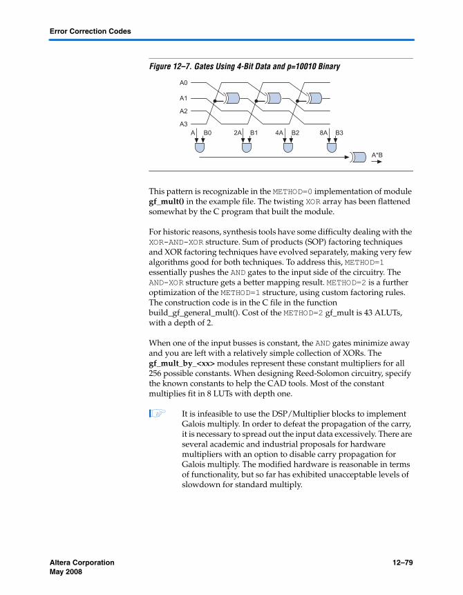
Altera Corporation MegaCore Version a.b.c variable 12–79May 2008
Error Correction Codes
Figure 12–7. Gates Using 4-Bit Data and p=10010 Binary
This pattern is recognizable in the METHOD=0 implementation of module gf_mult() in the example file. The twisting XOR array has been flattened somewhat by the C program that built the module.
For historic reasons, synthesis tools have some difficulty dealing with the XOR-AND-XOR structure. Sum of products (SOP) factoring techniques and XOR factoring techniques have evolved separately, making very few algorithms good for both techniques. To address this, METHOD=1 essentially pushes the AND gates to the input side of the circuitry. The AND-XOR structure gets a better mapping result. METHOD=2 is a further optimization of the METHOD=1 structure, using custom factoring rules. The construction code is in the C file in the function build_gf_general_mult(). Cost of the METHOD=2 gf_mult is 43 ALUTs, with a depth of 2.
When one of the input busses is constant, the AND gates minimize away and you are left with a relatively simple collection of XORs. The gf_mult_by_<xx> modules represent these constant multipliers for all 256 possible constants. When designing Reed-Solomon circuitry, specify the known constants to help the CAD tools. Most of the constant multiplies fit in 8 LUTs with depth one.
1 It is infeasible to use the DSP/Multiplier blocks to implement Galois multiply. In order to defeat the propagation of the carry, it is necessary to spread out the input data excessively. There are several academic and industrial proposals for hardware multipliers with an option to disable carry propagation for Galois multiply. The modified hardware is reasonable in terms of functionality, but so far has exhibited unacceptable levels of slowdown for standard multiply.
A0
A1
A2
A3A 2A 4A 8A
A*B
B0 B1 B2 B3

12–80 MegaCore Version a.b.c variable Altera CorporationMay 2008
Reed-Solomon Forward Error Correction (FEC)
Implementations in ROM are unattractive due to the large required address space—typically 16 inputs, or 64K words. This cost is reasonable if the ROM has numerous read ports, for example, 32. However, replacing just a few gf_mult units with a 64 Kbyte ROM is impractical.
Example files: ecc/reed_sol.v (search for “Galois field multiplier“)ecc/reed_sol.cpp (search for build_gf_general_mult)
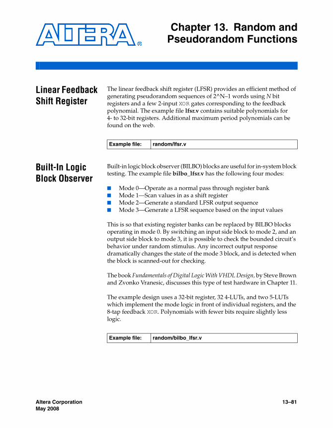
Altera Corporation MegaCore Version a.b.c variable 13–81May 2008
Chapter 13. Random andPseudorandom Functions
Linear Feedback Shift Register
The linear feedback shift register (LFSR) provides an efficient method of generating pseudorandom sequences of 2^N–1 words using N bit registers and a few 2-input XOR gates corresponding to the feedback polynomial. The example file lfsr.v contains suitable polynomials for 4- to 32-bit registers. Additional maximum period polynomials can be found on the web.
Built-In Logic Block Observer
Built-in logic block observer (BILBO) blocks are useful for in-system block testing. The example file bilbo_lfsr.v has the following four modes:
■ Mode 0—Operate as a normal pass through register bank■ Mode 1—Scan values in as a shift register■ Mode 2—Generate a standard LFSR output sequence■ Mode 3—Generate a LFSR sequence based on the input values
This is so that existing register banks can be replaced by BILBO blocks operating in mode 0. By switching an input side block to mode 2, and an output side block to mode 3, it is possible to check the bounded circuit’s behavior under random stimulus. Any incorrect output response dramatically changes the state of the mode 3 block, and is detected when the block is scanned-out for checking.
The book Fundamentals of Digital Logic With VHDL Design, by Steve Brown and Zvonko Vranesic, discusses this type of test hardware in Chapter 11.
The example design uses a 32-bit register, 32 4-LUTs, and two 5-LUTs which implement the mode logic in front of individual registers, and the 8-tap feedback XOR. Polynomials with fewer bits require slightly less logic.
Example file: random/lfsr.v
Example file: random/bilbo_lfsr.v
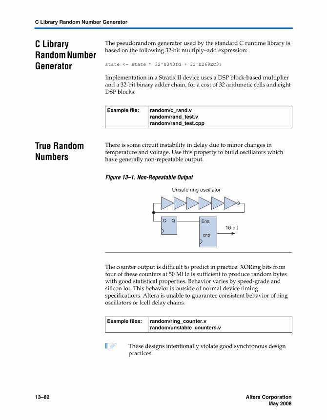
13–82 MegaCore Version a.b.c variable Altera CorporationMay 2008
C Library Random Number Generator
C Library Random Number Generator
The pseudorandom generator used by the standard C runtime library is based on the following 32-bit multiply–add expression:
state <= state * 32'h343fd + 32'h269EC3;
Implementation in a Stratix II device uses a DSP block-based multiplier and a 32-bit binary adder chain, for a cost of 32 arithmetic cells and eight DSP blocks.
True Random Numbers
There is some circuit instability in delay due to minor changes in temperature and voltage. Use this property to build oscillators which have generally non-repeatable output.
Figure 13–1. Non-Repeatable Output
The counter output is difficult to predict in practice. XORing bits from four of these counters at 50 MHz is sufficient to produce random bytes with good statistical properties. Behavior varies by speed-grade and silicon lot. This behavior is outside of normal device timing specifications. Altera is unable to guarantee consistent behavior of ring oscillators or lcell delay chains.
1 These designs intentionally violate good synchronous design practices.
Example file: random/c_rand.vrandom/rand_test.vrandom/rand_test.cpp
Example files: random/ring_counter.vrandom/unstable_counters.v
cntr
Ena16 bit
Unsafe ring oscillator
D Q

Altera Corporation MegaCore Version a.b.c variable 13–83May 2008
Random and Pseudorandom Functions
Race Condition-Based True Random Numbers
The most common approach for true random number generation on FPGAs is ring oscillator based. For security applications, it is common to use multiple independent rings. There is some concern that multiple rings on the same chip tends to synchronize over time. Any trend toward synchronization can create unwanted correlations in output. This design uses a different approach to eliminate the asynchronous ring oscillator.
The basic delay element is a carry chain fed by a one-hot decoder.
Figure 13–2. Variable Chain-Based Delay
The carry chain is wired to produce an output of “0” when the registers are cleared. When the registers are loaded with a “1”, it propagates from the entry point down to the output. The propagation time is selected by the one-hot decoder input.
Two of these variable delay chains drive the latch circuit shown in Figure 13–3. The output registers use the same clock as the chain input registers. The circuit is intended to meet timing for one clock cycle despite containing latches on the critical path.
One-H
ot
Register

13–84 MegaCore Version a.b.c variable Altera CorporationMay 2008
True Random Numbers
Figure 13–3. Output Latches
When the clear is released on the carry chain registers, the decoded “1” races down both chains. The latches detect which chain produced a “1” first. If the arrival times are sufficiently close, then neither latch is set. Theoretically, both latches can set, although this did not occur in experiments. The overall effect is a race condition with fine programmable timing. Most decoder settings produce consistent results (that is, always A first, always B first, always neither first) across trials. However there are a significant number of settings which have unstable results. In unstable cases, thermal and electrical noise influences whether a latch has time to set before the second signal arrives.
The example file chain_delay_race implements two variable chain delays and a latch circuit as described above, and contains a tiny state machine to run a continuous series of propagation trials.
To produce random numbers, the race circuit needs to use an unstable pair of one-hot decoder settings. Unstable settings tend to vary over time and operating temperature. It is possible that no unstable setting exists. For example, if the routing delays were grossly imbalanced, the delays may not overlap in the programmable range.
The chain_delay_adjust example iterates through settings and counts the number of A first and B first outputs over 255 trials. If the results are consistent, it changes the setting and reevaluates. For unstable settings it makes no adjustment but continues to evaluate. The adjusting output notifies the output filter when the circuit is experimenting with settings and is therefore predictable.
Example file: random/chain_delay_race.v
A firstchain "A"
chain "B "
reset
B first
stable
reset
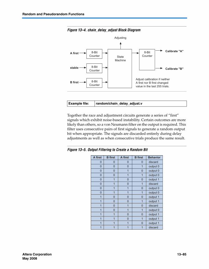
Altera Corporation MegaCore Version a.b.c variable 13–85May 2008
Random and Pseudorandom Functions
Figure 13–4. chain_delay_adjust Block Diagram
Together the race and adjustment circuits generate a series of “first” signals which exhibit noise-based instability. Certain outcomes are more likely than others, so a von Neumann filter on the output is required. This filter uses consecutive pairs of first signals to generate a random output bit when appropriate. The signals are discarded entirely during delay adjustments as well as when consecutive trials produce the same result.
Figure 13–5. Output Filtering to Create a Random Bit
Example file: random/chain_delay_adjust.v
A first Calibrate "A"
Calibrate "B"
8-BitCounter
stable 8-BitCounter
B first 8-BitCounter
8-BitCounter
Adjusting
Adjust calibration if neither A first nor B first changed value in the last 255 trials.
StateMachine
A first B first A first B first Behavior0000000011111111
0000111100001111
0011001100110011
0101010101010101
discardoutput 0output 0output 0output 1discardoutput 0output 0output 1output 1discardoutput 0output 1output 1output 1discard

13–86 MegaCore Version a.b.c variable Altera CorporationMay 2008
Word Stream Scrambling
Note that if the delay becomes predictable the output circuitry stops generating bits. If the stability persists, then the adjustment state machine switches to another setting. If there are no unstable settings, then the output never produces a bit rather than generating non-random bits.
The chain_delay_rand example file instantiates the race circuit using 32-bit chains with 16 delay selections each, an adjustment state machine, and an output filter.
Experiments with the combined example circuit on Cyclone II and Stratix II devices showed excellent balance for first, second, and third order bit distribution. Eight megabytes of binary sample data had zero compression. None of the chains failed to identify any unstable settings although several Stratix II chains frequently recalibrated. Increasing the number of calibration bits creates a higher chance of finding an unstable setting in return for a modest increase in area cost.
Word Stream Scrambling
The example file word_stream_scramble.v is based on a small C program that generates word scrambler/descramblers in Verilog HDL. The data stream enters a shift register serially and is multiplexed to the output in pseudo-random order producing a garbled data stream where each value appears within a fixed displacement of where it belongs (Figure 13–6).
Figure 13–6. Word Stream Scrambling
The C program randomly creates a shuffling pattern while guaranteeing no words are lost or duplicated, and builds an inverse pattern selectable by parameter. The tables are stored in the case statement at the bottom of the generated Verilog HDL (word_stream_scramble.v). For a period of 64 cycles, the pattern table fits conveniently into single 6-LUTs. The test bench demonstrates scrambling and unscrambling a counter sequence.
Example file: random/chain_delay_rand.v
Shift in
Randomized output
patterncounter
Altera Corporation MegaCore Version a.b.c variable 13–87May 2008
Random and Pseudorandom Functions
The logic is heavily pipelined for high speed operation. Note that if you change scrambling parameters by means other than word width, you must regenerate the Verilog HDL from C.
This type of scrambling is the easiest way to generate a pseudo-random stream with specific data distribution properties, and is suitable for low security encryption to make data streams non-standard. To improve the randomness, increase the period and maximum displacement parameters in the C program and replace the C runtime random number generator with a more sophisticated function, for example, RC4.
Example files: random/make_scrambler.cpprandom/word_stream_scramble.vrandom/word_stream_scramble_tb.v

13–88 MegaCore Version a.b.c variable Altera CorporationMay 2008
Word Stream Scrambling
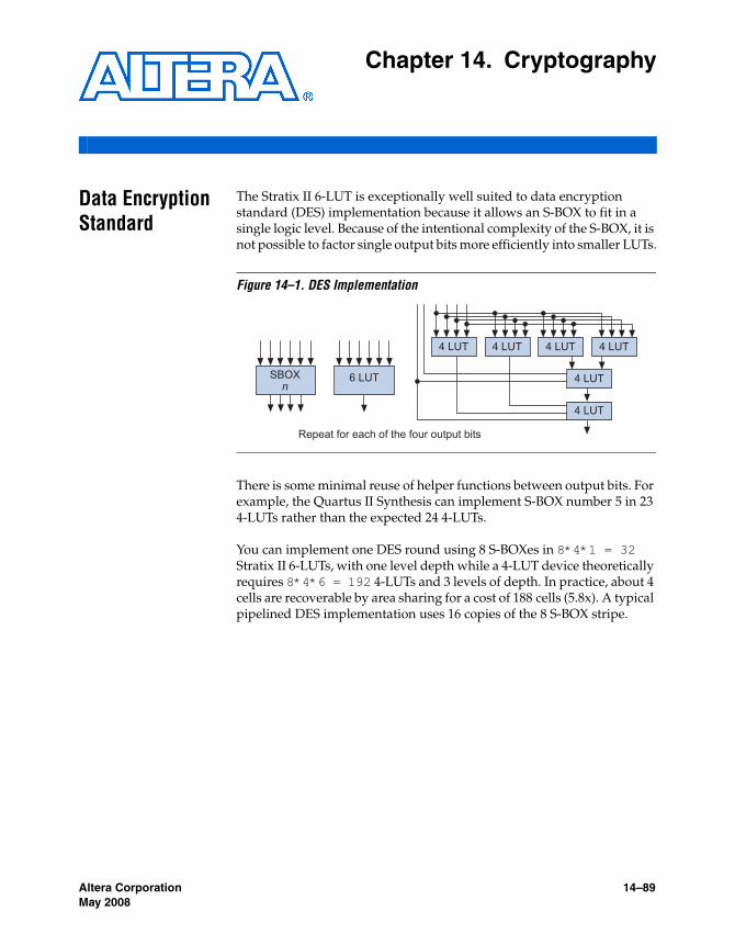
Altera Corporation MegaCore Version a.b.c variable 14–89May 2008
Chapter 14. Cryptography
Data Encryption Standard
The Stratix II 6-LUT is exceptionally well suited to data encryption standard (DES) implementation because it allows an S-BOX to fit in a single logic level. Because of the intentional complexity of the S-BOX, it is not possible to factor single output bits more efficiently into smaller LUTs.
Figure 14–1. DES Implementation
There is some minimal reuse of helper functions between output bits. For example, the Quartus II Synthesis can implement S-BOX number 5 in 23 4-LUTs rather than the expected 24 4-LUTs.
You can implement one DES round using 8 S-BOXes in 8*4*1 = 32 Stratix II 6-LUTs, with one level depth while a 4-LUT device theoretically requires 8*4*6 = 192 4-LUTs and 3 levels of depth. In practice, about 4 cells are recoverable by area sharing for a cost of 188 cells (5.8x). A typical pipelined DES implementation uses 16 copies of the 8 S-BOX stripe.
SBOXn
6 LUT
Repeat for each of the four output bits
4 LUT 4 LUT 4 LUT 4 LUT
4 LUT
4 LUT

14–90 MegaCore Version a.b.c variable Altera CorporationMay 2008
Data Encryption Standard
Figure 14–2. Pipelined DES Implementation
Each DES round is composed of an S-BOX array, an expansion permutation, a straight permutation, a 48-bit key XOR, and a 32-bit Feistel XOR. A DES encryption uses 16 rounds, with some minor initial and final permutation. Decryption uses the same hardware and a reversed key sequence.
Permutations are cumbersome to implement in software, but “free” in hardware. The following implementation of the DES round permute requires a change in wiring pattern and no lcells:
module permute (in,out);input [31:0] in;output [31:0] out;
wire [31:0] out;
assign out = {in[16],in[25],in[12],in[11],in[3],in[20],in[4],in[15],in[31],in[17],in[9],in[6],in[27],in[14],in[1],in[22],in[30],in[24],in[8],in[18],in[0],in[5],in[29],in[23],in[13],in[19],in[2],in[26],in[10],in[21],in[28],in[7]
};endmodule
When pipelining a DES circuit on Stratix II devices, it is important to place the registers so that the XORs can flatten together between adjacent rounds. This provides depth savings compared to the traditional placement at the round output.
This DES implementation uses a customized 16-level pipeline, selected by the PIPE_16B parameter. A new 64-bit data word, and key if desired, are used on each cycle. You must set the default optimization technique to SPEED. The resource usage is 2,543 ALUTs. Standalone operating
expand
32 bit
32 bit32 bit
48 bit
32 bit
Round key
32 bit
Permute
Eight S-BOXes

Altera Corporation MegaCore Version a.b.c variable 14–91May 2008
Cryptography
speed is 400 MHz, in-system speed degrades somewhat. You can select decryption by parameter. Selecting decryption does not change the operating speed or resource usage.
1 The example files use zero-based MSB first-word ordering internally in contrast to the DES standard document which uses a confusing mixture of numbering systems. The top-level interface is identical, but the permutation arrays may look backwards.
The DES key is 56 bits long, traditionally stored as 64 with 8 unused bits available for parity. This implementation produces synthesis warnings about the unused key input signals.
Triple DES Triple DES traditionally uses an encrypt-decrypt-encrypt pattern. The original motivation was to maintain compatibility with single DES systems by setting the keys to the same value. Security experts recommend the use of three separate keys for the three rounds.
Triple DES is easily implemented on Stratix II devices by placing three DES units in a series. Latency and resource usage are tripled, and speed and throughput remain relatively constant.
Double DES is not used due to an impractical attack that assumes the availability of 2^56 words of storage space. The book Applied Cryptography, by Bruce Schneier, discusses this issue as well as other DES-related topics.
UNIX Password Encryption
Traditional UNIX password implementations use a “one-way“ function that is 25 DES encryptions of zero, using the password string as a key. The algorithm includes a modification to the DES expansion step to make the hardware non-standard.
The inputs to the function are an 8-character password, and a 2-character “salt“ that controls the expansion adjustment. The output is an 11-character string that is stored with the two salt characters in front, as shown in the example on page 14–92.
Example files: crypto/des/round.vcrypto/des/sboxes.vcrypto/des/des.vcrypto/des/des_tb.v

14–92 MegaCore Version a.b.c variable Altera CorporationMay 2008
Advanced Encryption Standard/ Rijndael
Password: “foobar12”Salt: “A3”Encryption result: “LvH7gb4dV5Y”Stored: “A3LvH7gb4dV5Y”
The transformation between Verilog HDL strings and binary words is handled by helper functions in the example file ucrypt.v. Passwd_crypt() is the top module and uses the DES examples described above for encryption.
Advanced Encryption Standard/ Rijndael
The advanced encryption standard (AES) (FIPS publication 197, 2001) describes the Rijndael algorithm with some minor limits to block and key size parameters.
Table 14–1 shows a comparison of DES and AES-128.
Note that the fMAX values reflect the standalone pipelined cores running on small devices, and there is some inevitable degradation when the cores are plugged into real systems. These numbers are intended to give a ball-park rather than a guarantee. With double data width and half the speed, AES-128 has roughly the same data throughput as DES (about 3.2 billion bytes per second). In terms of security, the AES keyspace is more difficult to enumerate by a factor of 2^72, and the area requirement is equivalent to roughly six DES units.
Example file: crypto/des/ucrypt.vcrypto/des/des/des_tb.v
Table 14–1. DES and AES Comparison
Parameter Data Encryption Standard
Advanced Encryption Standard-128
key size 56 128
data size 64 128
Rounds 16 10
Round logic depth 2 4
Total ALUT 2543 15379
Typical fMAX 402 MHz 196 MHz
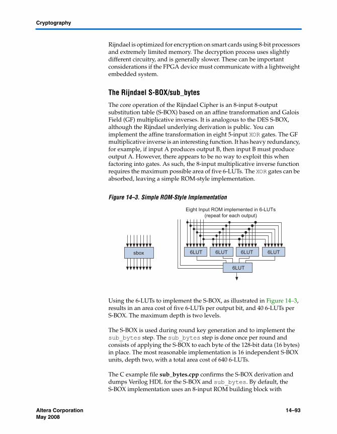
Altera Corporation MegaCore Version a.b.c variable 14–93May 2008
Cryptography
Rijndael is optimized for encryption on smart cards using 8-bit processors and extremely limited memory. The decryption process uses slightly different circuitry, and is generally slower. These can be important considerations if the FPGA device must communicate with a lightweight embedded system.
The Rijndael S-BOX/sub_bytes
The core operation of the Rijndael Cipher is an 8-input 8-output substitution table (S-BOX) based on an affine transformation and Galois Field (GF) multiplicative inverses. It is analogous to the DES S-BOX, although the Rijndael underlying derivation is public. You can implement the affine transformation in eight 5-input XOR gates. The GF multiplicative inverse is an interesting function. It has heavy redundancy, for example, if input A produces output B, then input B must produce output A. However, there appears to be no way to exploit this when factoring into gates. As such, the 8-input multiplicative inverse function requires the maximum possible area of five 6-LUTs. The XOR gates can be absorbed, leaving a simple ROM-style implementation.
Figure 14–3. Simple ROM-Style Implementation
Using the 6-LUTs to implement the S-BOX, as illustrated in Figure 14–3, results in an area cost of five 6-LUTs per output bit, and 40 6-LUTs per S-BOX. The maximum depth is two levels.
The S-BOX is used during round key generation and to implement the sub_bytes step. The sub_bytes step is done once per round and consists of applying the S-BOX to each byte of the 128-bit data (16 bytes) in place. The most reasonable implementation is 16 independent S-BOX units, depth two, with a total area cost of 640 6-LUTs.
The C example file sub_bytes.cpp confirms the S-BOX derivation and dumps Verilog HDL for the S-BOX and sub_bytes. By default, the S-BOX implementation uses an 8-input ROM building block with
sbox
Eight Input ROM implemented in 6-LUTs(repeat for each output)
6LUT 6LUT 6LUT 6LUT
6LUT

14–94 MegaCore Version a.b.c variable Altera CorporationMay 2008
Advanced Encryption Standard/ Rijndael
parameterized masks. You can override the METHOD parameter to use an unstructured version for testing or experimentation. The example file sub_bytes.v contains the generated Verilog HDL implementation.
Rijndael shift_rows
Rijndael shift_rows is a cyclic permutation that is done once per round. The 128-bit data represented here as 128'habcdefghijklmnop is treated as a 4-by-4 grid of bytes, and rotated by the rows as shown in the pattern in Figure 14–4.
Figure 14–4. Rotated 4-by-4 Byte Grid
The examples in show the rotation, inverse rotation, and a small C program used to build them. This permutation is free in hardware implementation.
Rijndael mix_columns and Round Keying
Rijndael mix_columns is the diffusion step of Rijndael. Each 4-byte column undergoes a GF constant polynomial multiply, making each of the four bytes a function of all the others.
assign s0_o = mult2(s0_i) ^ mult3(s1_i) ^ s2_i ^ s3_i;assign s1_o = s0_i ^ mult2(s1_i) ^ mult3(s2_i) ^ s3_i;assign s2_o = s0_i ^ s1_i ^ mult2(s2_i) ^ mult3(s3_i);assign s3_o = mult3(s0_i) ^ s1_i ^ s2_i ^ mult2(s3_i);
The multiplications are implemented in XOR gates. The support set is sufficiently large to require depth two in Stratix II LUTs. Four column mixing units are required for parallel operation.
Example files: crypto/aes/sub_bytes.cppcrypto/aes/sub_bytes.v
Example files: crypto/aes/shift_rows.cppcrypto/aes/shift_rows.v
ABCD
EFGH
IJKL
MNOP
AFKP
EJOD
INCH
MBGL

Altera Corporation MegaCore Version a.b.c variable 14–95May 2008
Cryptography
The final step of the round operation is to XOR the 128-bit round key with the 128-bit data. This array of 2-input XOR gates blends into the mix_columns operation with no increase in depth.
Rijndael Key Evolution
The round keys are derived from the user key through an iterative process composed of shifts, XORs, and the S-BOX. The exact procedure varies with the key size. The FIPS specification allows key sizes of 128, 192, and 256 bits. The example files contain 128 and 256 implementations, but not a 192 implementation.
Each round key evolution step uses four S-BOXes (160 6-LUTs) and 128 XOR gates of various widths up to 6-input. The maximum depth is three levels. The 256-bit version uses a simpler method on every other step. The KEY_EVOLVE_TYPE parameter is used to distinguish them.
Rijndael 128 Encipher
The example files implement a pipelined Rijndael encryption with 128-bit key according to the FIPS specification. Correctness is verified using the expected results in the specification appendix B. It has a latency of 10 cycles and can take new data and key on every cycle.
rijn_round_128.v implements a single round of encryption and key evolution. The merging of the key evolution with the round does not increase hardware cost, and allows the cipher to be rekeyed on-the-fly. The C program is a simple loop that generates ten of the round functions with the appropriate parameters. The example file aes_128.v is the output of the C program and implements the top level.
Example file: crypto/aes/mix_columns.v
Example file: crypto/aes/evolve_key.v
Example files: crypto/aes/aes_round_128.vcrypto/aes/aes_128.vcrypto/aes/aes_128.cppcrypto/aes/aes_128_tb.v

14–96 MegaCore Version a.b.c variable Altera CorporationMay 2008
Advanced Encryption Standard/ Rijndael
Rijndael 128 Decipher
Rijndael is built from invertible steps, so decryption is essentially applying inverse functions in reversed sequence. The example files contain all of the necessary inverse functions, for example, sub_bytes() and inv_sub_bytes(). The top level design aes_128.v also contains inv_aes_128 which performs the full pipelined decryption.
This decryption implementation uses an “inverse cipher key“ which is easily derived from the encryption process. aes_128 has an output port which delivers the appropriate inverse key along with the encryption result. This method is briefly referenced in the original AES proposal document section 5.3.4.1. It appears to be the only way to avoid ten cycles of “dead time” when a new decryption key is loaded. Due to inverse key use, the example implementation can be rekeyed on every cycle.
The inverse column mixing function is more complex than the forward version. It uses more area, but is still expected to absorb the key XORs and fit in two logic levels. The complete inverse round is four levels which is the same as the forward round. In practice, the decryption seems to be more difficult to route, and runs approximately 15 MHz to 20 MHz slower than encryption.
Rijndael 256-Bit Key Size (AES 256)
The 256-bit key requires an increase from 10 to 14 rounds, the latency of the pipeline increases by 10 to 14, and the logic area increases by approximately 40 percent. There are some relatively minor modifications to the key evolution circuitry. Note that every other key round behaves a bit differently.
Rijndael 192-Bit Key Size (AES 192)
To create this key size you must make modifications to the round schedule and the key evolution circuitry. The basic building blocks are the same as the 128- and 256-bit key size.
Example files: crypto/aes/aes_round_128.vcrypto/aes/aes_128.vcrypto/aes/aes_128.cppcrypto/aes/aes_128_tb.v
Example files: crypto/aes/aes_round_256.vcrypto/aes/aes_256.vcrypto/aes/aes_256.cppcrypto/aes/aes_256_tb.v

Altera Corporation MegaCore Version a.b.c variable 14–97May 2008
Cryptography
RC4 Stream This is an implementation of the RC4 stream cipher found in Applied Cryptography, by Bruce Schneier. This is a compact algorithm that takes a key up to 256 bytes long and generates a stream of random bytes. This implementation uses one dual-port 4K RAM block and 154 ALUTs. It operates at approximately 382 MHz and generates a byte every four clock cycles.
Figure 14–5. RC4 Stream Algorithm
The algorithm is well respected and is used in some large-scale commercial applications. There is an enable signal on the sample generator to facilitate running multiple generators out of phase to increase the effective output rate.
The example files contain the hardware implementation, an equivalent C software version for comparison, and a test bench. The RAM block is located in the altera_mf.v file in the <Quartus II installation directory>/eda/sim_lib directory.
Secure Hash Algorithm
The secure hash algorithm (SHA) is specified in FIPS 180-2. This standard describes several variations; only SHA-512 and SHA-384 are implemented in the example files.
SHA-512 is based on an 80-step iteration of shifts, adds, multiplexer, and majority functions. The first 16 rounds use 64-bit message words (1024 bits total). The subsequent 64 rounds use rotated combinations of previous message words. Each set of 80 rounds produces a hash value.
Example files: crypto/rc4/rc4.vcrypto/rc4/rc4.cppcrypto/rc4/rc4_tb.v
Byte stream
I
J
Statemachine
RAM256 byte
2 port
Key[256]
14–98 MegaCore Version a.b.c variable Altera CorporationMay 2008
Secure Hash Algorithm
The hash value accumulates until the message blocks are exhausted. There is a padding step to ensure that all messages are multiples of 1024 bits long. The hash output is the 512-bit accumulation.
SHA-384 is implemented as SHA-512, discarding the upper output bits. There is also a change to the initial state of the hash accumulator.
The algorithm is simple to follow. See Section 6.3 of the FIPS specification for the description. The example files contain a direct implementation. Each round uses 81 clock ticks (80 for evolution, one for hash accumulation). Message blocks are 64-bit and accepted on the first 16 cycles of each round. Implemented on a 2S60C3 device, this SHA512 uses 2083 ALUTs and operates at 130 MHz (205 M bytes per second). SHA384 is roughly the same. The full hash value must be accumulated despite discarding a portion at output time.
Message padding is done by adding a 1, followed by some number of zeros, followed by a 128-bit content length (in bits). The number of zeros is the minimum necessary for the total length to be a multiple of 1024 bits. The best padding method is application-specific. The example files contain a suitable padding front-end for SHA-384 and SHA-512.
The critical paths of SHA-512 run through the 64-bit adders. It is possible to pipeline these adders (see Chapter 1, Arithmetic). Pipelining increases the fMAX, but not the throughput. For higher throughput, formulate a 40 round version which evolves the abcdefgh register two steps in one tick. The arrangement of the e and a registers makes the formulation awkward. This is by design, the security depends on the difficulty of unrolling 80 rounds.
To improve the area in return for a small decrease in clock speed, the “K” table can be moved to ROM. The example file includes “synthesis preserve“ attributes on the K table input and output registers. This forces an implementation in approximately 192 LUTs. Removing the attributes allows ROM implementation.
Example files: crypto/sha/sha512.v (both 384 and 512 by parameter)crypto/sha/sha384_tb.vcrypto/sha/sha512_tb.v
Example files: crypto/sha/sha_padding.vcrypto/sha/sha_padding_tb.v
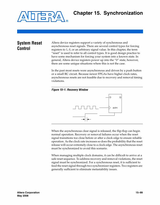
Altera Corporation MegaCore Version a.b.c variable 15–99May 2008
Chapter 15. Synchronization
System Reset Control
Altera device registers support a variety of synchronous and asynchronous reset signals. There are several control types for forcing registers to 1, 0, or an arbitrary signal value. In this chapter, the term “reset” is used to refer to all control types. It is good design practice to have some mechanism for forcing your system into a known state. In general, Altera device registers power up into the “0” state, however, there are some unique situations where this is not the case.
In the past most resets were asynchronous and driven by a push button or a small RC circuit. Because newer FPGAs have higher clock rates, asynchronous resets are not feasible due to recovery and removal timing violations.
Figure 15–1. Recovery Window
When the asynchronous clear signal is released, the flip-flop can begin normal operation. Recovery or removal failures occur when the reset signal transitions too close before or after a clock edge to ensure reliable operation. As the clock rate increases so does the probability that the reset release will occur extremely close to a clock edge. The asynchronous reset must be synchronized to avoid this scenario.
When managing multiple clock domains, it can be difficult to arrive at a safe reset sequence. To address recovery and removal violations, the reset signal must be synchronized. For a synchronous reset, it is sufficient to feed the reset signal through two synchronizer registers. Two registers are generally sufficient to eliminate metastability issues.
aclrn
D Q

15–100 MegaCore Version a.b.c variable Altera CorporationMay 2008
System Reset Control
Figure 15–2. Basic Synchronizer
In some cases, a basic reset synchronizer circuit is inadequate because the behavior requires the system clock to be stable, and the reset is not immediately asserted. For example, if the reset input is triggered by a loss of PLL lock, it is difficult to predict exactly when the synchronous reset will go active. The delay in activation can cause the malfunctioning system to go into logic contention with external devices. This problem can be corrected using the asynchronous reset hardware as shown in Figure 15–3.
Figure 15–3. Improved Reset Filter
In the circuit shown in Figure 15–3, the reset signal immediately forces the registers to “0”. If the clock is stopped, the system waits in the reset asserted state. After 2 ticks, the logical 1 propagates through and the reset is released. Because the release is synchronous to the clock there are no recovery/removal timing failures. The selection of an active low reset is convenient because the FPGA registers naturally power up to 0. This creates an automatic reset on power up. It is safe to cut the timing path from the external reset signal to the register aclr ports. The synchronized reset operates properly independent of the asynchronous input timing.
D QD Q
Synchronous ResetReset Button
System Clock
D QD Q
aclraclr
Synchronous Reset(Active Low)
Reset Button
System Clock

Altera Corporation MegaCore Version a.b.c variable 15–101May 2008
Synchronization
This reset filter is implemented in the example file.
The reset filter in Figure 15–3 is adequate for single trigger single clock domain situations. Typical FPGA systems need multiple reset triggers and multiple domain-specific reset outputs. To create a robust system, it is best to independently filter reset triggers before combining.
Figure 15–4. Combining Asynchronous Reset Triggers
Note that Altera registers support programmable inversion of the asynchronous clear port. Inverting reset signals does not incur any area or timing cost. Given the reset triggers are asynchronous, it is acceptable, in principle, combine the triggers before filtering, but the individual filter method shown in Figure 15–4 is viewed as more robust against glitching on the trigger signals.
Once a single system reset signal is available, it must be synchronized to each of the client clock domains. The same reset filtering circuit works for distribution, and has a convenient property where if the “1” in the filter registers is replaced with the previous filter’s output, the resets release sequentially. This is convenient for bringing up a multi-domain system in a reasonable deterministic order.
Example files: synchronization/reset_filter.v
D QD Q
aclraclr
sys_rstn
sys_clkrstn_button
D QD Q
aclraclr
pll_lock
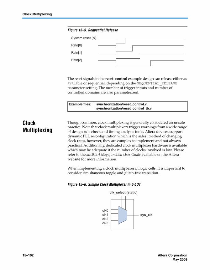
15–102 MegaCore Version a.b.c variable Altera CorporationMay 2008
Clock Multiplexing
Figure 15–5. Sequential Release
The reset signals in the reset_control example design can release either as available or sequential, depending on the SEQUENTIAL_RELEASE parameter setting. The number of trigger inputs and number of controlled domains are also parameterized.
Clock Multiplexing
Though common, clock multiplexing is generally considered an unsafe practice. Note that clock multiplexers trigger warnings from a wide range of design rule check and timing analysis tools. Altera devices support dynamic PLL reconfiguration which is the safest method of changing clock rates, however, they are complex to implement and not always practical. Additionally, dedicated clock multiplexer hardware is available which may be adequate if the number of clocks involved is low. Please refer to the altclkctrl Megafunction User Guide available on the Altera website for more information.
When implementing a clock multiplexer in logic cells, it is important to consider simultaneous toggle and glitch-free transition.
Figure 15–6. Simple Clock Multiplexer in 6-LUT
Example files: synchronization/reset_control.vsynchronization/reset_control_tb.v
System reset (N)
Rstn[0]
Rstn[1]
Rstn[2]
clk0clk1clk2clk3
clk_select (static)
sys_clk

Altera Corporation MegaCore Version a.b.c variable 15–103May 2008
Synchronization
The Altera datasheet statement is that LUT outputs may glitch during simultaneous toggle of input signals, independent of the LUT function. However, in practice the 4:1 multiplexer function does not generate any detectable glitches during simultaneous data input toggles. This property appears to hold when designs are converted to HardCopy II or similar logic cells. It is possible to construct cell implementations which exhibit significant glitches, so this simple clock multiplexer structure is not recommended. A further problem with this implementation is that the output behaves erratically during a change in the clk_select signals which can create timing violations on all registers fed by the system clock and possible metastability.
A more sophisticated clock select structure can eliminate the simultaneous toggle and switching problems.
Figure 15–7. Glitch Free Clock Multiplexer
This structure can be generalized for any number of clock channels. The clock_mux example contains a parameterized version. The circuit essentially enforces that no clock will activate until all others have been inactive for some time, and that activation will occur while the clock is low. Adding a synthesis_keep directive to the right hand side AND gates guarantees that there will be no simultaneous toggles on the input of the clk_out OR gate. It is important to note that switching from clock A to clock B requires that clock A continues to operate for at least a few cycles. If the old clock stops immediately the circuit gets stuck. The select signals are implemented as a one-hot control here, but they can easily be encoded. The input side logic is asynchronous and not critical. The circuit can tolerate extreme glitching during the switch process.
clk_out
sel0
sel1
clk1
clk0
DQ DQ DQ
DQ DQ DQ
Example files: synchronization/clock_mux.vsynchronization/clock_mux_tb.v

15–104 MegaCore Version a.b.c variable Altera CorporationMay 2008
Clock Multiplexing