stratix device handbook, volume 2, section 4, chapter … corporation 7–3 september 2004 stratix...
TRANSCRIPT
Altera Corporation 7–1September 2004
7. Implementing HighPerformance DSP Functions
in Stratix & Stratix GX Devices
Introduction Digital signal processing (DSP) is a rapidly advancing field. With products increasing in complexity, designers face the challenge of selecting a solution with both flexibility and high performance that can meet fast time-to-market requirements. DSP processors offer flexibility, but they lack real-time performance, while application-specific standard products (ASSPs) and application-specific integrated circuits (ASICs) offer performance, but they are inflexible. Only programmable logic devices (PLDs) offer both flexibility and high performance to meet advanced design challenges.
The mathematical theory underlying basic DSP building blocks—such as the finite impulse response (FIR) filter, infinite impulse response (IIR) filter, fast fourier transform (FFT), and direct cosine transform (DCT)—is computationally intensive. Altera® Stratix® and Stratix GX devices feature dedicated DSP blocks optimized for implementing arithmetic operations, such as multiply, multiply-add, and multiply-accumulate.
In addition to DSP blocks, Stratix and Stratix GX devices have TriMatrix™ embedded memory blocks that feature various sizes that can be used for data buffering, which is important for most DSP applications. These dedicated hardware features make Stratix and Stratix GX devices an ideal DSP solution.
This chapter describes the implementation of high performance DSP functions, including filters, transforms, and arithmetic functions, using Stratix and Stratix GX DSP blocks. The following topics are discussed:
■ FIR filters■ IIR filters■ Matrix manipulation■ Discrete Cosine Transform■ Arithmetic functions
Stratix & Stratix GX DSP Block Overview
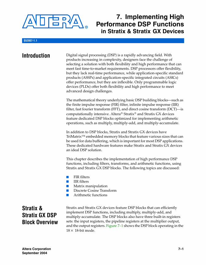
Stratix and Stratix GX devices feature DSP blocks that can efficiently implement DSP functions, including multiply, multiply-add, and multiply-accumulate. The DSP blocks also have three built-in registers sets: the input registers, the pipeline registers at the multiplier output, and the output registers. Figure 7–1 shows the DSP block operating in the 18 × 18-bit mode.
S52007-1.1
7–2 Altera CorporationStratix Device Handbook, Volume 2 September 2004
Stratix & Stratix GX DSP Block Overview
Figure 7–1. DSP Block Diagram for 18 x 18-bit Mode
Adder/Subtractor/
Accumulator2
Adder/Subtractor/
Accumulator1
Summation
Optional PipelineRegister Stage
Multiplier Stage
Output SelectionMultiplexer
Optional Output Register Stage
CLRN
D Q
ENA
CLRN
D Q
ENA
CLRN
D Q
ENA
CLRN
D Q
ENA
CLRN
D Q
ENA
CLRN
D Q
ENA
CLRN
D Q
ENA
CLRN
D Q
ENA
CLRN
D Q
ENA
CLRN
D Q
ENA
CLRN
D Q
ENA
CLRN
D Q
ENA
Optional Serial Shift RegisterInputs from Previous DSP Block
Optional Stage Configurableas Accumulator or DynamicAdder/Subtractor
Summation Stagefor Adding FourMultipliers Together
Optional Input RegisterStage with Parallel Input orShift Register Configuration
Optional Serial Shift Register Outputs to Next DSP Blockin the Column
to MultiTrackInterconnect

Altera Corporation 7–3September 2004 Stratix Device Handbook, Volume 2
Implementing High Performance DSP Functions in Stratix & Stratix GX Devices
The DSP blocks are organized into columns enabling efficient horizontal communication with adjacent TriMatrix memory blocks. Tables 7–1 and 7–2 show the DSP block resources in Stratix and Stratix GX devices, respectively.
Table 7–1. DSP Block Resources in Stratix Devices
Device DSP Blocks Maximum 9 × 9 Multipliers
Maximum 18 × 18 Multipliers
Maximum 36 × 36 Multipliers
EP1S10 6 48 24 6
EP1S20 10 80 40 10
EP1S25 10 80 40 10
EP1S30 12 96 48 12
EP1S40 14 112 56 14
EP1S60 18 144 72 18
EP1S80 22 176 88 22
Table 7–2. DSP Block Resources in Stratix GX Devices
Device DSP Blocks Maximum 9 × 9 Multipliers
Maximum 18 × 18 Multipliers
Maximum 36 × 36 Multipliers
EP1SGX10C 6 48 24 6
EP1SGX10D 6 48 24 6
EP1SGX25C 10 80 40 10
EP1SGX25D 10 80 40 10
EP1SGX25F 10 80 40 10
EP1SGX40D 14 112 56 14
EP1SGX40G 14 112 56 14
7–4 Altera CorporationStratix Device Handbook, Volume 2 September 2004
TriMatrix Memory Overview
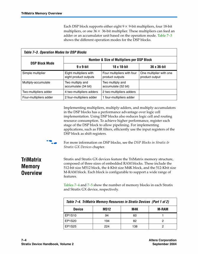
Each DSP block supports either eight 9 × 9-bit multipliers, four 18-bit multipliers, or one 36 × 36-bit multiplier. These multipliers can feed an adder or an accumulator unit based on the operation mode. Table 7–3 shows the different operation modes for the DSP blocks.
Implementing multipliers, multiply-adders, and multiply-accumulators in the DSP blocks has a performance advantage over logic cell implementation. Using DSP blocks also reduces logic cell and routing resource consumption. To achieve higher performance, register each stage of the DSP block to allow pipelining. For implementing applications, such as FIR filters, efficiently use the input registers of the DSP block as shift registers.
f For more information on DSP blocks, see the DSP Blocks in Stratix & Stratix GX Devices chapter.
TriMatrix Memory Overview
Stratix and Stratix GX devices feature the TriMatrix memory structure, composed of three sizes of embedded RAM blocks. These include the 512-bit size M512 block, the 4-Kbit size M4K block, and the 512-Kbit size M-RAM block. Each block is configurable to support a wide range of features.
Tables 7–4 and 7–5 show the number of memory blocks in each Stratix and Stratix GX device, respectively.
Table 7–3. Operation Modes for DSP Blocks
DSP Block ModeNumber & Size of Multipliers per DSP Block
9 x 9-bit 18 x 18-bit 36 x 36-bit
Simple multiplier Eight multipliers with eight product outputs
Four multipliers with four product outputs
One multiplier with one product output
Multiply-accumulate Two multiply and accumulate (34 bit)
Two multiply and accumulate (52 bit)
Two-multipliers adder 4 two-multipliers adders 2 two-multipliers adders
Four-multipliers adder 2 four-multipliers adder 1 four-multipliers adder
Table 7–4. TriMatrix Memory Resources in Stratix Devices (Part 1 of 2)
Device M512 M4K M-RAM
EP1S10 94 60 1
EP1S20 194 82 2
EP1S25 224 138 2

Altera Corporation 7–5September 2004 Stratix Device Handbook, Volume 2
Implementing High Performance DSP Functions in Stratix & Stratix GX Devices
Most DSP applications require local data storage for intermediate buffering or for filter storage. The TriMatrix memory blocks enable efficient use of available resources for each application.
The M512 and M4K memory blocks can implement shift registers for applications, such as multi-channel filtering, auto-correlation, and cross-correlation functions. Implementing shift registers in embedded memory blocks reduces logic cell and routing resource consumption.
f For more information on TriMatrix memory blocks, see the TriMatrix Embedded Memory Blocks in Stratix & Stratix GX Devices chapter.
DSP Function Overview
The following sections describe commonly used DSP functions. Each section illustrates the implementation of a basic DSP building block, including FIR and IIR filters, in Stratix and Stratix GX devices using DSP blocks and TriMatrix memory blocks.
Finite Impulse Response (FIR) Filters
This section describes the basic theory and implementation of basic FIR filters, time-domain multiplexed (TDM) FIR filters, and interpolation and decimation polyphase FIR filters. An introduction to the complex FIR filter is also presented in this section.
EP1S30 295 171 4
EP1S40 384 183 4
EP1S60 574 292 6
EP1S80 767 364 9
Table 7–5. TriMatrix Memory Resources in Stratix GX Devices
Device M512 M4K M-RAM
EP1SGX10C 94 60 1
EP1SGX10D 94 60 1
EP1SGX25C 224 138 2
EP1SGX25D 224 138 2
EP1SGX25F 224 138 2
EP1SGX40D 384 183 4
EP1SGX40G 384 183 4
Table 7–4. TriMatrix Memory Resources in Stratix Devices (Part 2 of 2)
Device M512 M4K M-RAM
7–6 Altera CorporationStratix Device Handbook, Volume 2 September 2004
Finite Impulse Response (FIR) Filters
FIR Filter Background
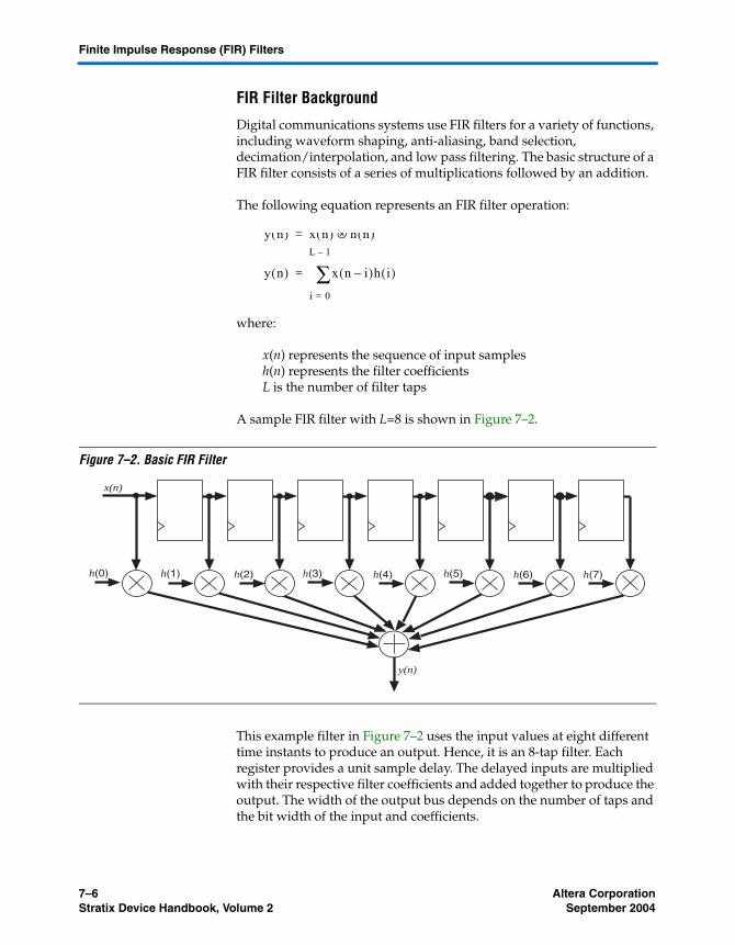
Digital communications systems use FIR filters for a variety of functions, including waveform shaping, anti-aliasing, band selection, decimation/interpolation, and low pass filtering. The basic structure of a FIR filter consists of a series of multiplications followed by an addition.
The following equation represents an FIR filter operation:
where:
x(n) represents the sequence of input samplesh(n) represents the filter coefficientsL is the number of filter taps
A sample FIR filter with L=8 is shown in Figure 7–2.
Figure 7–2. Basic FIR Filter
This example filter in Figure 7–2 uses the input values at eight different time instants to produce an output. Hence, it is an 8-tap filter. Each register provides a unit sample delay. The delayed inputs are multiplied with their respective filter coefficients and added together to produce the output. The width of the output bus depends on the number of taps and the bit width of the input and coefficients.
y n( ) x n( ) h n( )⊗=
y n( ) x n i–( )h i( )
i 0=
L 1–
∑=
x(n)
y(n)
h(2)h(1) h(3) h(4) h(5) h(6) h(7)h(0)

Altera Corporation 7–7September 2004 Stratix Device Handbook, Volume 2
Implementing High Performance DSP Functions in Stratix & Stratix GX Devices
Basic FIR Filter
A basic FIR filter is the simplest FIR filter type. As shown in Figure 7–2, a basic FIR filter has a single input channel and a single output channel.
Basic FIR Filter Implementation
Stratix and Stratix GX devices’ dedicated DSP blocks can implement basic FIR filters. Because these DSP blocks have closely integrated multipliers and adders, filters can be implemented with minimal routing resources and delays. For implementing FIR filters, the DSP blocks are configured in the four-multipliers adder mode.
f See the DSP Blocks in Stratix & Stratix GX Devices chapter for more information on the different modes of the DSP blocks.
This section describes the implementation of an 18-bit 8-tap FIR filter. Because Stratix and Stratix GX devices support modularity, cascading two 4-tap filters can implement an 8-tap filter. Larger FIR filters can be designed by extending this concept. Users can also increase the number of taps available per DSP block if 18 bits of resolution are not required. For example, by using only 9 bits of resolution for input samples and coefficient values, 8 multipliers are available per DSP block. Therefore, a 9-bit 8-tap filter can be implemented in a single DSP block provided an external adder is implemented in logic cells.
The four-multipliers adder mode, shown in Figure 7–3, provides four 18 × 18-bit multipliers and three adders in a single DSP block. Hence, it can implement a 4-tap filter. The data width of the input and the coefficients is 18 bits, which results in a 38-bit output for a 4-tap filter.

7–8 Altera CorporationStratix Device Handbook, Volume 2 September 2004
Finite Impulse Response (FIR) Filters
Figure 7–3. Hardware View of a DSP Block in Four-Multipliers Adder Mode Notes (1). (2), (3)
Notes to Figure 7–3:(1) The input registers feed the multiplier blocks. These registers can increase the DSP block performance, but are
optional. These registers can also function as shift registers if the dedicated shiftin/shiftout signals are used.(2) The pipeline registers are fed by the multiplier blocks. These registers can increase the DSP block performance, but
are optional.(3) The output registers register the DSP block output. These registers can increase the DSP block performance, but are
optional.
D Q
D Q
D Q
D Q
D Q
D Q
D Q
D Q
18
18
18
18
18
18
18
18
18
18
18
36
36
36
36
37
37
38
Outputy(n)
x(n)
h(0)
x(n-1)
h(1)
x(n-2)
h(2)
x(n-3)
h(3) Multiplier D
Multiplier C
Multiplier B
Multiplier A
CLK1CLR1
CLK2CLR2
shiftoutinput fromprevious
block
shiftout input fromprevious
block
Data from row
interface block
Coefficients from row interface
block
shiftininput to
next block
shiftininput to
next block
Data from rowinterface block
Data from rowinterface block
Data from rowinterface block
Coefficients from rowinterface
block
Coefficients from row interface
block
Coefficients from row interface
block
18
18
18
18
18
D Q
D Q
D Q
D Q
D Q38

Altera Corporation 7–9September 2004 Stratix Device Handbook, Volume 2
Implementing High Performance DSP Functions in Stratix & Stratix GX Devices
Figure 7–4. Quartus II Software View of MegaWizard Implementation of a DSP Block in Four-Multipliers Adder Mode
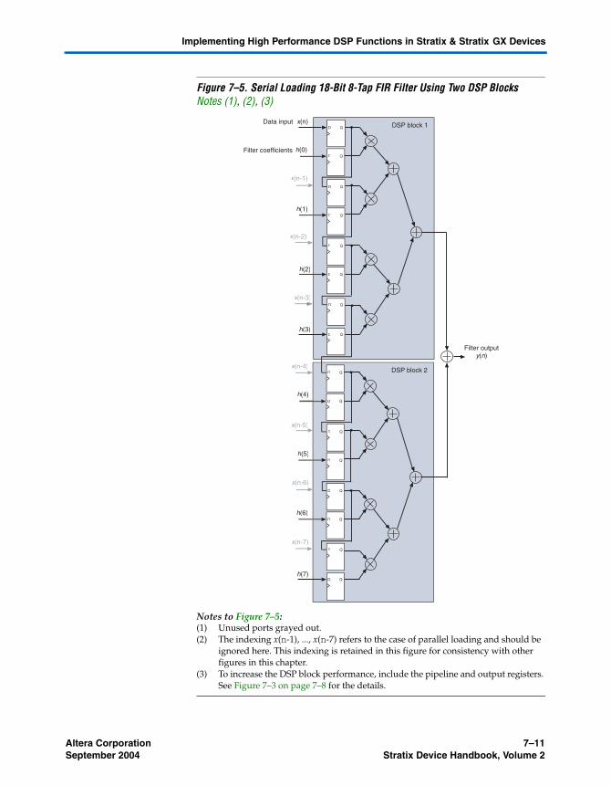
Each input register of the DSP block provides a shiftout output that connects to the shiftin input of the adjacent input register of the same DSP block. The registers on the boundaries of a DSP block also connect to the registers of adjacent DSP blocks through the use of shiftin/shiftout connections. These connections create register chains spanning multiple DSP blocks, which makes it easy to increase the length of FIR filters. Figure 7–5 shows two DSP blocks connected to create an 8-tap FIR filter. Filters with more taps can be implemented by connecting DSP blocks in a similar manner, provided sufficient DSP blocks are available in the device.
1 Adding the outputs of the two DSP blocks requires an external adder which can be implemented using logic cells.
The input data can be fed directly or by using the shiftout/shiftin chains, which allow a single input to shift down the register chain inside the DSP block. The input to each of the registers has a multiplexer, hence, the data can be fed either from outside the DSP block or the preceding register. This can be selected from the MegaWizard® in the Quartus® II software, as shown in Figure 7–4. The example in Figure 7–5 uses the shiftout/shiftin flip-flop chains where the multiplexers are configured to use these chains. In this example, the flip-flops inside the DSP blocks serve as the taps of the FIR filter.
7–10 Altera CorporationStratix Device Handbook, Volume 2 September 2004
Finite Impulse Response (FIR) Filters
When the coefficients are loaded in parallel, they can be fed directly from memory elements or any other muxing scheme. This facilitates the implementation of an adaptive (variable) filter.
Further, if the user wants to implement the shift register chains external to the DSP block, this can be done by using the altshift_taps megafunction. In this case, the coefficient and data shifting is done external to the DSP block. The DSP block is only used to implement the multiplications and the additions.
Parallel vs. Serial ImplementationThe fastest implementations are fully parallel, but consume more logic resources than serial implementations. To trade-off performance for logic resources, implement a serial scheme with a specified number of taps. To facilitate this, Altera provides the FIR Compiler core through its MegaCore program. The FIR Compiler is an easy-to-use, fully-integrated graphical user interface (GUI) based FIR filter design software.
f For more information on the FIR Compiler MegaCore, visit the Altera web site at www.altera.com and search for “FIR compiler” in the “Intellectual Property” page.
It is important to note that the four-multipliers adder mode allows a DSP block to be configured for parallel or serial input. When it is configured for parallel input, as shown in Figure 7–6, the data input and the coefficients can be loaded directly without the need for shiftin/shiftout chains between adjacent registers in the DSP block. When the DSP block is configured for serial input, as shown in Figure 7–5, the shiftin/shiftout chains create a register cascade both within the DSP block and also between adjacent DSP blocks.
Altera Corporation 7–11September 2004 Stratix Device Handbook, Volume 2
Implementing High Performance DSP Functions in Stratix & Stratix GX Devices
Figure 7–5. Serial Loading 18-Bit 8-Tap FIR Filter Using Two DSP Blocks Notes (1), (2), (3)
Notes to Figure 7–5:(1) Unused ports grayed out.(2) The indexing x(n-1), ..., x(n-7) refers to the case of parallel loading and should be
ignored here. This indexing is retained in this figure for consistency with other figures in this chapter.
(3) To increase the DSP block performance, include the pipeline and output registers. See Figure 7–3 on page 7–8 for the details.
D Q
D Q
D Q
D Q
D Q
D Q
D Q
D Q
DSP block 1
Filter outputy(n)
h(0)
h(1)
h(2)
h(3)
x(n)
Filter coefficients
Data input
x(n-2)xx
x(n-3)xx
x(n-1)xx
h(4)
h(5)
h(6)
h(7)
x(n-4)xx
x(n-5)xx
x(n-6)xx
x(n-7)xx
D Q
D Q
D Q
D Q
D Q
D Q
D Q
D Q
DSP block 2

7–12 Altera CorporationStratix Device Handbook, Volume 2 September 2004
Finite Impulse Response (FIR) Filters
Figure 7–6. Parallel Loading 18-Bit 8-Tap FIR Filter Using Two DSP Blocks Notes (1), (2)
Notes to Figure 7–6:(1) The indexing x(n-1), ..., x(n-7) refers to the case of parallel loading.(2) To increase the DSP block performance, include the input, pipeline, and output
registers. See Figure 7–3 on page 7–8 for the details.
D Q
D Q
D Q
D Q
D Q
D Q
D Q
D Q
DSP block 1
Filter outputy(n)
h(0)
h(1)
h(2)
h(3)
x(n)
Filter coefficients
Data input
x(n-2)
x(n-3)
x(n-1)
h(4)
h(5)
h(6)
h(7)
x(n-4)
x(n-5)
x(n-6)
x(n-7)
D Q
D Q
D Q
D Q
D Q
D Q
D Q
D Q
DSP block 2
Altera Corporation 7–13September 2004 Stratix Device Handbook, Volume 2
Implementing High Performance DSP Functions in Stratix & Stratix GX Devices
Basic FIR Filter Implementation Results
Table 7–6 shows the results of the serial implementation of an 18-bit 8 tap FIR filter as shown in Figure 7–5 on page 7–11
Basic FIR Filter Design Example
Download the Basic FIR Filter (base_fir.zip) design example from the Design Examples section of the Altera web site at www.altera.com.
Time-Domain Multiplexed FIR Filters
A TDM FIR filter is clocked n-times faster than the sample rate in order to reuse the same hardware. Consider the 8-tap filter shown in Figure 7–2. The TDM technique can be used with a TDM factor of 2, i.e., n = 2, to implement this filter using only four multipliers, provided the filter is clocked two times faster internally.
To understand this concept, consider Figure 7–7 that shows a TDM filter with a TDM factor of 2. A 2× -multiplied clock is required to run the filter. On cycle 0 of the 2× clock, the user loads four coefficients into the four multiplier inputs. The resulting output is stored in a register. On cycle 1 of the 2× clock, the user loads the remaining four coefficients into the multiplier inputs. The output of cycle 1 is added with the output of cycle 0 to create the overall output. See the “TDM Filter Implementation” on page 7–14 section for details on the coefficient loading schedule.
The TDM implementation shown in Figure 7–7 requires only four multipliers to achieve the functionality of an 8-tap filter. Thus, TDM is a good way to save logic resources, provided the multipliers can run at n-times the clock speed. The coefficients can be stored in ROM/RAM, or any other muxing scheme.
Table 7–6. Basic FIR Filter Implementation Results
Part EP1S10F780
Utilization LCELL: 130/10570 (1%)DSP Block 9-bit elements: 16/48 (33%)Memory bits: 288/920448 (<1%)
Performance 247 MHz

7–14 Altera CorporationStratix Device Handbook, Volume 2 September 2004
Finite Impulse Response (FIR) Filters
Figure 7–7. Block Diagram of 8-Tap FIR Filter with TDM Factor of n=2
TDM Filter Implementation
TDM FIR filters are implemented in Stratix and Stratix GX devices by configuring the DSP blocks in the multiplier-adder mode. Figure 7–9 shows the implementation of an 8-tap TDM FIR filter (n=2) with 18 bits of data and coefficient inputs. Because the input data needs to be loaded into the DSP block in parallel, a shift register chain is implemented using a combination of logic cells and the altshift_taps function. This shift register is clocked with the same data sample rate (clock 1× ). The filter coefficients are stored in ROM and loaded into the DSP block in parallel as well. Because the TDM factor is 2, both the ROM and DSP block are clocked with clock 2× .
Figure 7–8 and Table 7–7 show the coefficient loading schedule. For example, during cycle 0, only the flip-flops corresponding to h(1), h(3), h(5), and h(7) are enabled. This produces the temporary output, y0, which is stored in a flip-flop outside the DSP block. During cycle 1, only the flip-
D QFIR filter with four multipliers18-bit input
2x clock
Output
Table 7–7. Operation of TDM Filter (Shown in Figure 7–9 on page 7–16)
Cycle of 2× Clock
Cycle Output Operation Overall Output, y(n)
0 y0 = x(n-1)h(1) + x(n-3)h(3) + x(n-5)h(5) + x(n-7)h(7) Store result N/A
1 y1 = x(n)h(0) + x(n-2)h(2) + x(n-4)h(4) + x(n-6)h(6) Generate output y(n) = y0 + y1
2 y2 = x(n)h(1) + x(n-2)h(3) + x(n-4)h(5) + x(n-6)h(7) Store result N/A
3 y3 = x(n+1)h(0) + x(n-1)h(2) + x(n-3)h(4) + x(n-5)h(6) Generate output y(n) = y2 + y3
4 y4 = x(n+1)h(1) + x(n-1)h(3) + x(n-3)h(5) + x(n-5)h(7) Store result N/A
5 y5 = x(n+2)h(0) + x(n)h(2) + x(n-2)h(4) + x(n-4)h(6) Generate output y(n) = y4 + y5
6 y6 = x(n+2)h(1) + x(n)h(3) + x(n-2)h(5) + x(n-4)h(7) Store result N/A
7 y7 = x(n+3)h(0) + x(n+1)h(2) + x(n-1)h(4) + x(n-3)h(6) Generate output y(n) = y6 + y7

Altera Corporation 7–15September 2004 Stratix Device Handbook, Volume 2
Implementing High Performance DSP Functions in Stratix & Stratix GX Devices
flops corresponding to h(0), h(2), h(4) and h(6) are enabled. This produces the temporary output, y1, which is added to y0 to produce the overall output, y(n). The following shows what the overall output, y(n), equals:
This is identical to the output of the 8-tap filter shown in Figure 7–2. After cycle 1, this process is repeated at every cycle.
Figure 7–8. Coefficient Loading Schedule in a TDM Filter
y n( ) y0 y1+=
y n( ) x 0( )h 0( ) x n 1–( )h 1( ) x n 2–( )h 2( ) x n 3–( )h 3( )+ + +=
+ x n 4–( )h 4( ) x n 5–( )h 5( ) x n 6–( )h 6( ) x n 7–( )h 7( )+ + +
Cycle 0
load h(1), h(3), h(5), h(7)
Cycle 1
load h(0), h(2), h(4), h(6)
Cycle 2
load h(1), h(3), h(5), h(7)
Cycle 3
load h(0), h(2), h(4), h(6)
Cycle 4
load h(1), h(3), h(5), h(7)
2x clock
1x clock

7–16 Altera CorporationStratix Device Handbook, Volume 2 September 2004
Finite Impulse Response (FIR) Filters
Figure 7–9. TDM FIR Filter Implementation Note (1)
Note to Figure 7–9:(1) To increase the DSP block performance, include the pipeline and output registers. See Figure 7–3 on page 7–8 for
details.
If the TDM factor is more than 2, then a multiply-accumulator needs to be implemented. This multiply-accumulator can be implemented using the soft logic outside the DSP block if all the multipliers of the DSP block are needed. Alternatively, the multiply-accumulator may be implemented inside the DSP block if all the multipliers of the DSP block are not needed. The accumulator needs to be zeroed at the start of each new sample input. The user also needs a way to store additional sample inputs in memory. For example, consider a sample rate of r and TDM factor of 4. Then, the
Filter outputy(n)
Clock input(1x clock)
1x clock
PLL
D Q
D Q
D Q
D Q
D Q
D Q
D Q
D Q
2x clock
x(n)xx DSP blockData input
RAM / ROM 0
RAM / ROM 1
RAM / ROM 2
RAM / ROM 3
Filter coefficients
D Q
Accumulator
D Q
D Q
D Q
D Q
D Q
D Q
D Q
Shift register

Altera Corporation 7–17September 2004 Stratix Device Handbook, Volume 2
Implementing High Performance DSP Functions in Stratix & Stratix GX Devices
user needs a way to accept this sample data and send it at a 4r rate to the input of the DSP block. One way to do this is using a first-in-first-out (FIFO) memory with input clocked at rate r and output clocked at rate 4r. The FIFO may be implemented in the TriMatrix memory.
TDM Filter Implementation Results
Table 7–8 shows the results of the implementation of an 18-bit 8-tap TDM FIR filter as shown in Figure 7–9 on page 7–16.
TDM Filter Design Example
Download the TDM FIR Filter (tdm_fir.zip) design example from the Design Examples section of the Altera web site at www.altera.com.
Polyphase FIR Interpolation Filters
An interpolation filter can be used to increase sample rate. An interpolation filter is efficiently implemented with a polyphase FIR filter. DSP systems frequently use polyphase filters because they simplify overall system design and also reduce the number of computations per cycle required of the hardware. This section first describes interpolation filters and then how to implement them as polyphase filters in Stratix and Stratix GX devices. See the “Polyphase FIR Decimation Filters” on page 7–24 section for a discussion of decimation filters.
Interpolation Filter Basics
An interpolation filter increases the output sample rate by a factor of I through the insertion if I-1 zeros between input samples, a process known as zero padding. After the zero padding, the output samples in time domain are separated by Ts/I = 1/(I×fs), where Ts and fs are the sample period and sample frequency of the original signal, respectively. Figure 7–10 shows the concept of signal interpolation.
Table 7–8. TDM Filter Implementation Results
Part EP1S10F780
Utilization Lcell: 196/10570 (1%)DSP Block 9-bit elements: 8/48 (17%)Memory bits: 360/920448 (<1%)
Performance 240 MHz (1)
Note to Table 7–8:(1) This refers to the performance of the DSP blocks. The input and output rate is 120
million samples per second (MSPS), clocked in and out at 120 MHz.

7–18 Altera CorporationStratix Device Handbook, Volume 2 September 2004
Finite Impulse Response (FIR) Filters
Inserting zeros between the samples creates reflections of the original spectrum, thus, a low pass filter is needed to filter out the reflections.
Figure 7–10. Block Diagram Representation of Interpolation
To see how interpolation filters work, consider the Nyquist Sampling Theorem. This theorem states that the maximum frequency of the input to be sampled must be smaller than fs/2, where fs is the sampling frequency, to avoid aliasing. This frequency, fs/2, is also known as the Nyquist frequency (Fn). Typically, before a signal is sampled using an analog to digital converter (ADC), it needs to be low pass filtered using an analog anti-aliasing filter to prevent aliasing. If the input frequency spectrum extends close to the Nyquist frequency, then the first alias is also close to the Nyquist frequency. Therefore, the low pass filter needs to be very sharp to reject this alias. A very sharp analog filter is hard to design and manufacture and could increase passband ripple, thereby compromising system performance.
The solution is to increase the sampling rate of the ADC, so that the new Nyquist frequency is higher and the spacing between the desired signal and the alias is also higher. Zero padding as described above increase the sample rate. This process also known as upsampling (oversampling) relaxes the roll off requirements of the anti-aliasing filter. Consequently, a simpler filter achieves alias suppression. A simpler analog filter is easier to implement, does not compromise system performance, and is also easier to manufacture.
Similarly, the digital to analog converter (DAC) typically interpolates the data before the digital to analog conversion. This relaxes the requirement on the analog low pass filter at the output of the DAC.
The interpolation filter does not need to run at the oversampled (upsampled) rate of fs× I. This is because the extra sample points added are zeros, so they do not contribute to the output.
Figure 7–11 shows the time and frequency domain representation of interpolation for a specific case where the original signal spectrum is limited to 2 MHz and the interpolation factor (I) is 4. The Nyquist frequency of the upsampled signal must be greater than 8 MHz, and is chosen to be 9 MHz for this example.
ILPF
Input Outputsample rate fs sample rate I*fs

Altera Corporation 7–19September 2004 Stratix Device Handbook, Volume 2
Implementing High Performance DSP Functions in Stratix & Stratix GX Devices
Figure 7–11. Time & Frequency Domain Representations of Interpolation for I = 4
As an example, CD players use interpolation, where the nominal sample rate of audio input is 44.1 kilosamples per second. A typical implementation might have an interpolation (oversampling) factor of 4 generating 176.4 kilosamples per second of oversampled data stream.
Polyphase Interpolation Filters
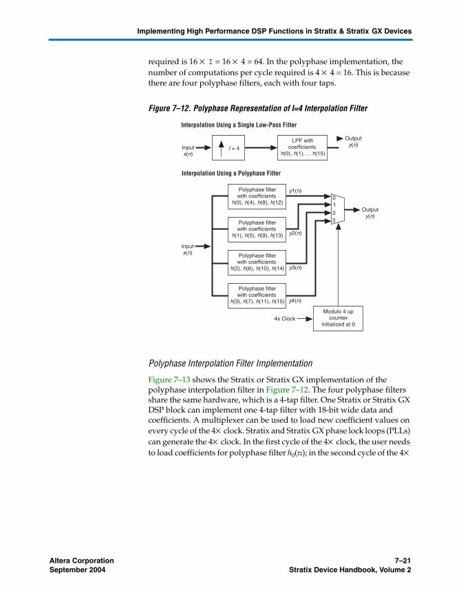
A direct implementation of an interpolation filter, as shown in Figure 7–10, imposes a high computational burden. For example, if the filter is 16 taps long and a multiplication takes one cycle, then the number of computations required per cycle is 16× I. Depending on the interpolation factor (I), this number can be quite big and may not be achievable in hardware. A polyphase implementation of the low pass filter can reduce the number of computations required per cycle, often by a large factor, as will be evident later in this section.
The polyphase implementation “splits” the original filter into I polyphase filters whose impulse responses are defined by the following equation:
hk n( ) h k nI+( )=

7–20 Altera CorporationStratix Device Handbook, Volume 2 September 2004
Finite Impulse Response (FIR) Filters
where:
k = 0,1, …, I-1n = 0,1, …, P-1P = L/I = length of polyphase filtersL = length of the filter (selected to be a multiple of I)I = interpolation factorh(n) = original filter impulse response
This equation implies that the first polyphase filter, h0(n), has coefficients h(0), h(I), h(2I),..., h((P-1)I). The second polyphase filter, h1(n), has coefficients h(1), h(1+I), h(1+2I), ..., h(1+(P-1)I). Continuing in this way, the last polyphase filter, hI-1(n), has coefficients h(I-1), h((I - 1) + N), h((I - 1) + 2I), ..., h((I - 1) + (P-1)I).
An example helps in understanding the polyphase implementation of interpolation. Consider the polyphase representation of a 16-tap low pass filter with an interpolation factor of 4. Thus, the output is given below:
Referring back to Figure 7–11 on page 7–19, the only nonzero samples of the input are x(0), x(4), x(8,) and x(12). The first output, y(0), only depends on h(0), h(4), h(8) and h(12) because x(i) is zero for i ≠ 0, 4, 8, 12. Table 7–9 shows the coefficients required to generate output samples.
Table 7–9 shows that this filter operation can be represented by four parallel polyphase filters. This is shown in Figure 7–12. The outputs from the filters are multiplexed to generate the overall output. The multiplexer is controlled by a counter, which counts up modulo-I starting at 0.
It is illuminating to compare the computational requirements of the direct implementation versus polyphase implementation of the low pass filter. In the direct implementation, the number of computations per cycle
y n( ) h n iI–( )x i( )
i 0=
15
∑=
Table 7–9. Decomposition of a 16-Tap Interpolating Filter into Four Polyphase Filters
Output Sample Coefficients Required Polyphase Filter Impulse Response
y(0), y(4)... h(0), h(4), h(8), h(12) h0(n)
y(1), y(5)... h(1), h(5), h(9), h(13) h1(n)
y(2), y(6)... h(2), h(6), h(10), h(14) h2(n)
y(3), y(7)... h(3), h(7), h(11), h(15) h3(n)
Altera Corporation 7–21September 2004 Stratix Device Handbook, Volume 2
Implementing High Performance DSP Functions in Stratix & Stratix GX Devices
required is 16 × I = 16 × 4 = 64. In the polyphase implementation, the number of computations per cycle required is 4 × 4 = 16. This is because there are four polyphase filters, each with four taps.
Figure 7–12. Polyphase Representation of I=4 Interpolation Filter
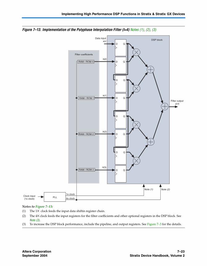
Polyphase Interpolation Filter Implementation
Figure 7–13 shows the Stratix or Stratix GX implementation of the polyphase interpolation filter in Figure 7–12. The four polyphase filters share the same hardware, which is a 4-tap filter. One Stratix or Stratix GX DSP block can implement one 4-tap filter with 18-bit wide data and coefficients. A multiplexer can be used to load new coefficient values on every cycle of the 4× clock. Stratix and Stratix GX phase lock loops (PLLs) can generate the 4× clock. In the first cycle of the 4× clock, the user needs to load coefficients for polyphase filter h0(n); in the second cycle of the 4×
I = 4LPF with
coefficients h(0), h(1), ... h(15)
Inputx(n)
Outputy(n)
Interpolation Using a Single Low-Pass Filter
Interpolation Using a Polyphase Filter
Polyphase filterwith coefficients
h(0), h(4), h(8), h(12)
Polyphase filterwith coefficients
h(1), h(5), h(9), h(13)
Polyphase filterwith coefficients
h(2), h(6), h(10), h(14)
Polyphase filterwith coefficients
h(3), h(7), h(11), h(15)
Outputy(n)
Inputx(n)
y1(n)
y2(n)
y3(n)
y4(n)
Modulo 4 upcounter
initialized at 04x Clock
01
23

7–22 Altera CorporationStratix Device Handbook, Volume 2 September 2004
Finite Impulse Response (FIR) Filters
clock, the users needs to load coefficients of the polyphase filter h1(n) and so on. Table 7–10 summarizes the coefficient loading schedule. The output, y(n), is clocked using the 4× clock.
Table 7–10. Polyphase Interpolation (I=4) Filter Coefficient Loading Schedule
Cycle of 4× Clock Coefficients to Load Corresponding RAM/ROM
1, 5,... h(0), h(4), h(8), h(12) 0, 1, 2, 3
2, 6,... h(1), h(5), h(9), h(13) 0, 1, 2, 3
3, 7,... h(2), h(6), h(10), h(14) 0, 1, 2, 3
4, 8,... h(3), h(7), h(11), h(15) 0, 1, 2, 3
Altera Corporation 7–23September 2004 Stratix Device Handbook, Volume 2
Implementing High Performance DSP Functions in Stratix & Stratix GX Devices
Figure 7–13. Implementation of the Polyphase Interpolation Filter (I=4) Notes (1), (2), (3)
Notes to Figure 7–13:(1) The 1× clock feeds the input data shiftin register chain.
(2) The 4× clock feeds the input registers for the filter coefficients and other optional registers in the DSP block. See Note (3).
(3) To increase the DSP block performance, include the pipeline, and output registers. See Figure 7–3 for the details.
h(0)
h(1)
h(2)
h(3)
Filter outputy(n)
Note (2)
Clock input(1x clock)
1x clockPLL
D Q
D Q
D Q
D Q
D Q
D Q
D Q
D Q
4x clock
Note (1)
x(n)xx DSP blockData input
RAM / ROM 0
RAM / ROM 1
RAM / ROM 2
RAM / ROM 3
Filter coefficients

7–24 Altera CorporationStratix Device Handbook, Volume 2 September 2004
Finite Impulse Response (FIR) Filters
Polyphase Interpolation Filter Implementation Results
Table 7–11 shows the results of the polyphase interpolation filter implementation in a Stratix device shown in Figure 7–13.
Polyphase Interpolation Filter Design Example
Download the Interpolation FIR Filter (interpolation_fir.zip) design example from the Design Examples section of the Altera web site at www.altera.com.
Polyphase FIR Decimation Filters
A decimation filter can be used to decrease the sample rate. A decimation filter is efficiently implemented with a polyphase FIR filter. DSP systems frequently use polyphase filters because they simplify overall system design and also reduce the number of computations per cycle required of the hardware. This section first describes decimation filters and then how to implement them as polyphase filters in Stratix devices. See the “Polyphase FIR Interpolation Filters” section for a discussion of interpolation filters.
Decimation Filter Basics
A decimation filter decreases the output sample rate by a factor of D through keeping only every D-th input sample. Consequently, the samples at the output of the decimation filter are separated by D× Ts= D/fs, where Ts and fs are the sample period and sample frequency of the original signal, respectively. Figure 7–14 shows the concept of signal decimation.
The signal needs to be low pass filtered before downsampling can begin in order to avoid the reflections of the original spectrum from being aliased back into the output signal.
Table 7–11. Polyphase Interpolation Filter Implementation Results
Part EP1S10F780
Utilization Lcell: 3/10570 (<1%)DSP Block 9-bit elements: 8/48 (17%)Memory bits: 288/920448 (<1%)
Performance 240 MHz (1)
Note to Table 7–11:(1) This refers to the performance of the DSP blocks, as well as the output clock rate.
The input rate is 60 MSPS, clocked in at 60MHz.

Altera Corporation 7–25September 2004 Stratix Device Handbook, Volume 2
Implementing High Performance DSP Functions in Stratix & Stratix GX Devices
Figure 7–14. Block Diagram Representation of Decimation
Decimation filters reverse the effect of the interpolation filters. Before the decimation process, a low pass filter is applied to the signal to attenuate noise and aliases present beyond the Nyquist frequency. The filtered signal is then applied to the decimation filter, which processes every D-th input. Therefore the values between samples D, D-1, D-2 etc. are ignored. This allows the filter to run M times slower than the input data rate.
In a typical system, after the analog to digital conversion is complete, the data needs to be filtered to remove aliases inherent in the sampled data. Further, at this point there is no need to continue to process this data at the higher sample (oversampled) rate. Therefore, a decimation FIR filter at the output of the ADC lowers the data rate to a value that can be processed digitally.
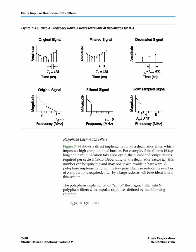
Figure 7–15 shows a specific example where a signal spread over 8 MHz is decimated by a factor of 4 to 2 MHz. The Nyquist frequency of the downsampled signal must be greater than 2 MHz, and is chosen to be 2.25 MHz in this example.
DLPF
Input Outputsample rate fs sample rate fs/D
7–26 Altera CorporationStratix Device Handbook, Volume 2 September 2004
Finite Impulse Response (FIR) Filters
Figure 7–15. Time & Frequency Domain Representations of Decimation for D=4
Polyphase Decimation Filters
Figure 7–14 shows a direct implementation of a decimation filter, which imposes a high computational burden. For example, if the filter is 16 taps long and a multiplication takes one cycle, the number of computations required per cycle is 16× D. Depending on the decimation factor (D), this number can be quite big and may not be achievable in hardware. A polyphase implementation of the low pass filter can reduce the number of computations required, often by a large ratio, as will be evident later in this section.
The polyphase implementation “splits” the original filter into D polyphase filters with impulse responses defined by the following equation.
hk n( ) h k nD+( )=
Altera Corporation 7–27September 2004 Stratix Device Handbook, Volume 2
Implementing High Performance DSP Functions in Stratix & Stratix GX Devices
where:
k = 0,1, …, D-1n = 0,1, …, P-1P = L/D = length of polyphase filtersL is the length of the filter (selected to be a multiple of D)D is the decimation factorh(n) is the original filter impulse response
This equation implies that the first polyphase filter, h0(n), has coefficients h(0), h(D), h(2D)…h((P-1)D). The second polyphase filter, h1(n), has coefficients h(1), h(1+D), h(1+2D), ..., h(1+(P-1)D). Continuing in this way, the last polyphase filter, hD-1(n) has coefficients h(D-1), h((D - 1) + D),h((D - 1) + 2D), ..., h((D - 1) + (P-1)D).
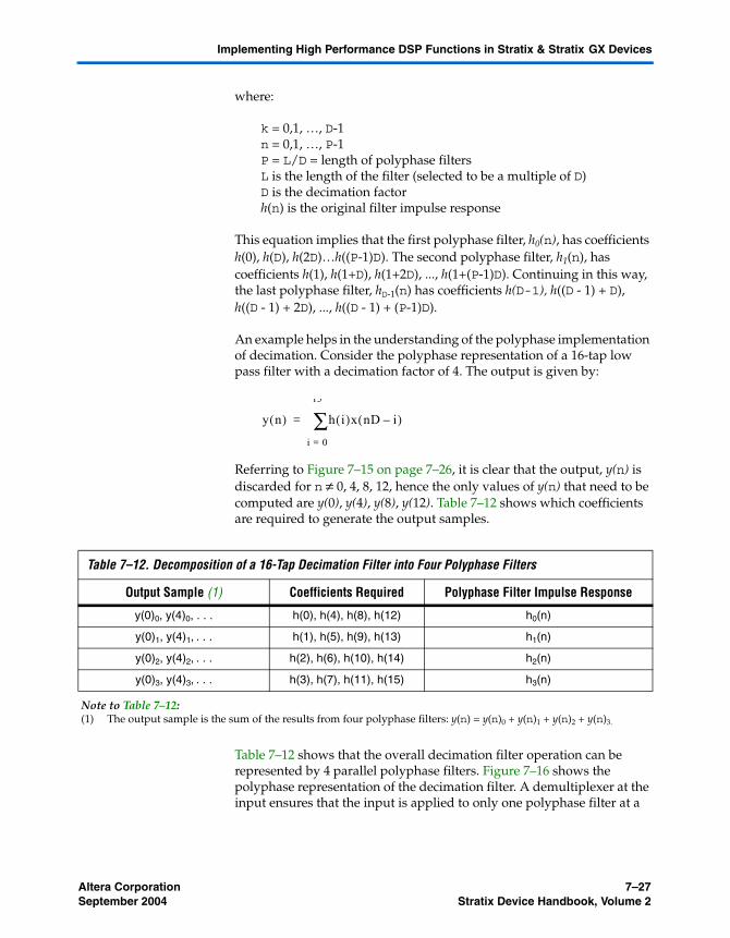
An example helps in the understanding of the polyphase implementation of decimation. Consider the polyphase representation of a 16-tap low pass filter with a decimation factor of 4. The output is given by:
Referring to Figure 7–15 on page 7–26, it is clear that the output, y(n) is discarded for n ≠ 0, 4, 8, 12, hence the only values of y(n) that need to be computed are y(0), y(4), y(8), y(12). Table 7–12 shows which coefficients are required to generate the output samples.
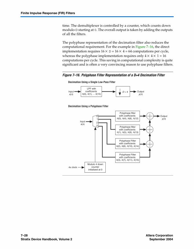
Table 7–12 shows that the overall decimation filter operation can be represented by 4 parallel polyphase filters. Figure 7–16 shows the polyphase representation of the decimation filter. A demultiplexer at the input ensures that the input is applied to only one polyphase filter at a
y n( ) h i( )x nD i–( )
i 0=
15
∑=
Table 7–12. Decomposition of a 16-Tap Decimation Filter into Four Polyphase Filters
Output Sample (1) Coefficients Required Polyphase Filter Impulse Response
y(0)0, y(4)0, . . . h(0), h(4), h(8), h(12) h0(n)
y(0)1, y(4)1, . . . h(1), h(5), h(9), h(13) h1(n)
y(0)2, y(4)2, . . . h(2), h(6), h(10), h(14) h2(n)
y(0)3, y(4)3, . . . h(3), h(7), h(11), h(15) h3(n)
Note to Table 7–12:(1) The output sample is the sum of the results from four polyphase filters: y(n) = y(n)0 + y(n)1 + y(n)2 + y(n)3.
7–28 Altera CorporationStratix Device Handbook, Volume 2 September 2004
Finite Impulse Response (FIR) Filters
time. The demultiplexer is controlled by a counter, which counts down modulo-D starting at 0. The overall output is taken by adding the outputs of all the filters.
The polyphase representation of the decimation filter also reduces the computational requirement. For the example in Figure 7–16, the direct implementation requires 16 × D = 16 × 4 = 64 computations per cycle, whereas the polyphase implementation requires only 4 × 4 × 1 = 16 computations per cycle. This saving in computational complexity is quite significant and is often a very convincing reason to use polyphase filters.
Figure 7–16. Polyphase Filter Representation of a D=4 Decimation Filter
D = 4LPF with
coefficients h(0), h(1), ... h(15)
Inputx(n)
Outputy(n)
Decimation Using a Single Low-Pass Filter
Decimation Using a Polyphase Filter
Polyphase filterwith coefficients
h(0), h(4), h(8), h(12)
Polyphase filterwith coefficients
h(1), h(5), h(9), h(13)
Polyphase Filterwith coefficients
h(2), h(6), h(10), h(14)
Polyphase Filterwith coefficients
h(3), h(7), h(11), h(15)
Outputy(n)
Inputx(n)
Modulo 4 downcounter
initialized at 04x clock
01
23
Altera Corporation 7–29September 2004 Stratix Device Handbook, Volume 2
Implementing High Performance DSP Functions in Stratix & Stratix GX Devices
Polyphase Decimation Filter Implementation
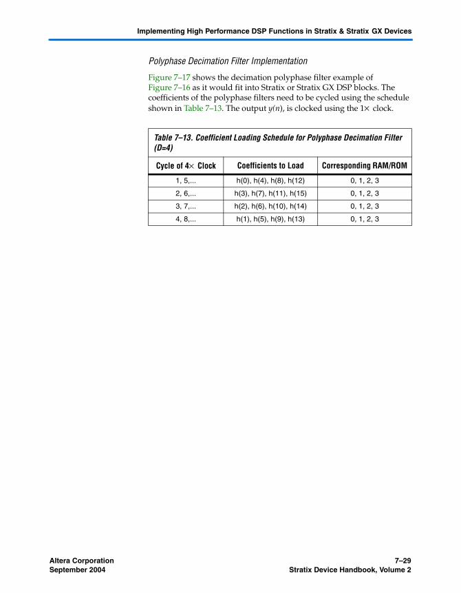
Figure 7–17 shows the decimation polyphase filter example of Figure 7–16 as it would fit into Stratix or Stratix GX DSP blocks. The coefficients of the polyphase filters need to be cycled using the schedule shown in Table 7–13. The output y(n), is clocked using the 1× clock.
Table 7–13. Coefficient Loading Schedule for Polyphase Decimation Filter (D=4)
Cycle of 4× Clock Coefficients to Load Corresponding RAM/ROM
1, 5,... h(0), h(4), h(8), h(12) 0, 1, 2, 3
2, 6,... h(3), h(7), h(11), h(15) 0, 1, 2, 3
3, 7,... h(2), h(6), h(10), h(14) 0, 1, 2, 3
4, 8,... h(1), h(5), h(9), h(13) 0, 1, 2, 3

7–30 Altera CorporationStratix Device Handbook, Volume 2 September 2004
Finite Impulse Response (FIR) Filters
Figure 7–17. Implementation of the Polyphase Decimation Filter (D=4) Notes (1), (2), (3)
Notes to Figure 7–17:(1) The 1× clock feeds the register after the accumulator block.
(2) The 4× clock feeds the shift register for the data, the input registers for both the data and filter coefficients, the other optional registers in the DSP block (see Note (3)), and the accumulator block.
(3) To increase the DSP block performance, include the pipeline, and output registers. See Figure 7–3 on page 7–8 for the details.
Filter outputy(n)
Note (2)
Clock input(1x clock)
ROM
ROM
ROM
ROM
1x clockPLL
D Q
D Q
D Q
D Q
D Q
D Q
D Q
D Q
4x clock
Note (1)
DSP block
Filtercoefficients
x(n)xxData input
D Q
D Q
D Q
D Q
D Q
D Q
D Q
D Q
D Q
D Q
D Q
D Q
D Q
D Q

Altera Corporation 7–31September 2004 Stratix Device Handbook, Volume 2
Implementing High Performance DSP Functions in Stratix & Stratix GX Devices
Polyphase Decimation Filter Implementation Results
Table 7–14 shows the results of the polyphase decimation filter implementation in a Stratix device shown in Figure 7–17.
Polyphase Decimation Filter Design Example
Download the Decimation FIR Filter (decimation_fir.zip) design example from the Design Examples section of the Altera web site at www.altera.com.
Complex FIR Filter
A complex FIR filter takes real and imaginary input signals and performs the filtering operation with real and imaginary filter coefficients. The output also consists of real and imaginary signals. Therefore, a complex FIR filter is similar to a regular FIR filter except for the fact that the input, output, and coefficients are all complex numbers.
One example application of complex FIR filters is equalization. Consider a Phase Shift Keying (PSK) system; a single complex channel can represent the I and Q data channels. A FIR filter with complex coefficients could then process both data channels simultaneously. The filter coefficients are chosen in order to reverse the effects of intersymbol interference (ISI) inherent in practical communication channels. This operation is called equalization. Often, the filter is adaptive, i.e. the filter coefficients can be varied as desired, to optimize performance with varying channel characteristics.
A complex variable FIR filter is a cascade of complex multiplications followed by a complex addition. Figure 7–18 shows a block diagram representation of a complex FIR filter. To compute the overall output of the FIR filter, it is first necessary to determine the output of each complex multiplier. This can be expressed as:
Table 7–14. Polyphase Decimation Filter Implementation Results
Part EP1S10F780
Utilization Lcell: 168/10570 (1%)DSP Block 9-bit elements: 8/48 (17%)Memory bits: 300/920448(<1%)
Performance 240 MHz (1)
Note to Table 7–14:(1) This refers to the performance of the DSP blocks, as well as the input clock rate.
The output rate is 60 MSPS (clocked out at 60MHz).

7–32 Altera CorporationStratix Device Handbook, Volume 2 September 2004
Finite Impulse Response (FIR) Filters
where:
xreal is the real input signalximag is the imaginary input signalhreal is the real filter coefficientshimag is the imaginary filter coefficientsyreal is the real output signalyimag is the imaginary output signal
In complex representation, this equals:
The overall real channel output is obtained by adding the real channel outputs of all the multipliers. Similarly, the overall imaginary channel output is obtained by adding the imaginary channel outputs of all the multipliers.
Figure 7–18. Complex FIR Filter Block Diagram
Complex FIR Filter Implementation
Complex filters can be easily implemented in Stratix devices with the DSP blocks configured in the two-multipliers adder mode. One DSP block can implement a 2-tap complex FIR filter with 9-bit inputs, or a single tap complex FIR filter with 18-bit inputs. DSP blocks can be cascaded to implement complex filters with more taps.
1 The two-multipliers adder mode has two adders, each adding the outputs of two multipliers. One of the adders is configured as a subtractor.
yreal xreal hreal× ximag himag×–=
yimag xreal himag× hreal ximag×+=
yreal jyimag+ xreal jximag+( ) hreal jhimag+( )×=
ComplexFIR filter
xreal
ximag
yreal
yimag
hreal himag

Altera Corporation 7–33September 2004 Stratix Device Handbook, Volume 2
Implementing High Performance DSP Functions in Stratix & Stratix GX Devices
f For more information on the different modes of the DSP blocks, see the DSP Blocks in Stratix & Stratix GX Devices chapter.
Figure 7–19 shows an example of a 2-tap complex FIR filter design with 18-bit inputs. The real and the complex outputs of the DSP blocks are added externally to generate the overall real and imaginary output. As in the case of basic, TDM, or polyphase FIR filters, the coefficients may be loaded in series or parallel.
Figure 7–19. 2-Tap 18-Bit Complex FIR Filter Implementation
DSP block Configured as a subtractor
himag1
hreal1
ximag1
xreal1
outreal1 = xreal1 * hreal1 - ximag1 * himag1
outimag1 = xreal1 * himag1 + ximag1 * hreal1
Configured as a adder
DSP block Configured as a subtractor
himag2
hreal2
ximag2
xreal2
outreal2 = xreal2 * hreal2 - ximag2 * himag2
outimag2 = xreal2 * himag2 + ximag2 * hreal2
Configured as a adder
Overall real output
Overall imaginary output

7–34 Altera CorporationStratix Device Handbook, Volume 2 September 2004
Infinite Impulse Response (IIR) Filters
Infinite Impulse Response (IIR) Filters
Another class of digital filters are IIR filters. These are recursive filters where the current output is dependent on previous outputs. In order to maintain stability in an IIR filter, careful design consideration must be given, especially to the effects of word-length to avoid unbounded conditions. The following section discusses the general theory and applications behind IIR Filters.
IIR Filter Background
The impulse response of an IIR filter extends for an infinite amount of time because their output is based on feedback from previous outputs. The general expression for IIR filters is:
where ai and bi represent the coefficients in the feed-forward path and feedback path, respectively, and n represents the filter order. These coefficients determine where the poles and zeros of the IIR filter lie. Consequently, they also determine how the filter functions (i.e., cut-off frequencies, band pass, low pass, etc.).
The feedback feature makes IIR filters useful in high data throughput applications that require low hardware usage. However, feedback also introduces complications and caution must be taken to make sure these filters are not exposed to situations in which they may become unstable. The complications include phase distortion and finite word length effects, but these can be overcome by ensuring that the filter always operates within its intended range.
Figure 7–20 shows a direct form II structure of an IIR filter.
y n( ) a i( )x n i–( )
i 0=
n
∑ b i( )y n i–( )
i 1=
n
∑–=

Altera Corporation 7–35September 2004 Stratix Device Handbook, Volume 2
Implementing High Performance DSP Functions in Stratix & Stratix GX Devices
Figure 7–20. Direct Form II Structure of an IIR Filter
The transfer function for an IIR filter is:
The numerator contains the zeros of the filter and the denominator contains the poles. The IIR filter structure requires a multiplication followed by an accumulation. Constructing the filter directly from the transfer function shown above may result in finite word length limitations and make the filter potentiality unstable. This becomes more critical as the filter order increases, because it only has a finite number of bits to represent the output. To prevent overflow or instability, the transfer function can be split into two or more terms representing several second order filters called biquads. These biquads can be individually scaled and cascaded, splitting the poles into multiples of two. For example, an IIR filter having ten poles should be split into five biquad sections. Doing this minimizes quantization and recursive accumulation errors.
X(n) Σ
-b1a1Σ
Σ
Σ
Z-1
Z-1
Z-1
Σ
Σ
Σ
Σ
-b2
-bn
Y(n)
a2
an
a0w(n)
H z( )
aizi–
i 0=
n
∑
1 bizi–
i 1=
n
∑+
------------------------------=
7–36 Altera CorporationStratix Device Handbook, Volume 2 September 2004
Infinite Impulse Response (IIR) Filters
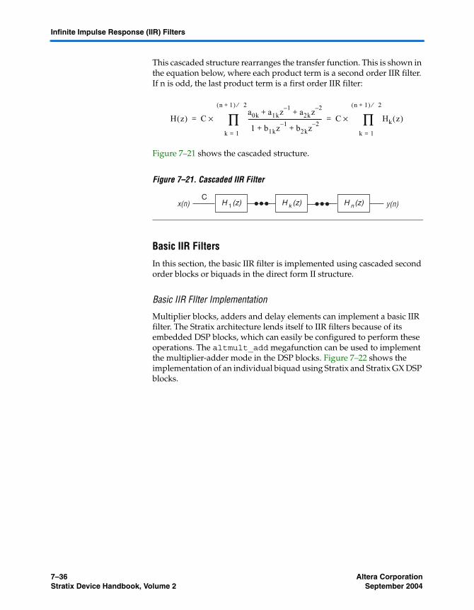
This cascaded structure rearranges the transfer function. This is shown in the equation below, where each product term is a second order IIR filter. If n is odd, the last product term is a first order IIR filter:
Figure 7–21 shows the cascaded structure.
Figure 7–21. Cascaded IIR Filter
Basic IIR Filters
In this section, the basic IIR filter is implemented using cascaded second order blocks or biquads in the direct form II structure.
Basic IIR FIlter Implementation
Multiplier blocks, adders and delay elements can implement a basic IIR filter. The Stratix architecture lends itself to IIR filters because of its embedded DSP blocks, which can easily be configured to perform these operations. The altmult_add megafunction can be used to implement the multiplier-adder mode in the DSP blocks. Figure 7–22 shows the implementation of an individual biquad using Stratix and Stratix GX DSP blocks.
H z( ) Ca0k a1kz 1– a+ 2kz 2–
+
1 b1kz 1– b2kz 2–+ +
----------------------------------------------------
k 1=
n 1+( ) 2⁄
∏× C Hk z( )
k 1=
n 1+( ) 2⁄
∏×= =
x(n) y(n)H (z)1 H (z)k H (z)nC

Altera Corporation 7–37September 2004 Stratix Device Handbook, Volume 2
Implementing High Performance DSP Functions in Stratix & Stratix GX Devices
Figure 7–22. IIR Filter Biquad Note (1)
Note to Figure 7–22:(1) Unused ports are grayed out.

7–38 Altera CorporationStratix Device Handbook, Volume 2 September 2004
Infinite Impulse Response (IIR) Filters
The first DSP block in Figure 7–22 is configured in the two-multipliers adder mode, and the second DSP block is in the four-multipliers adder mode. For an 18-bit input to the IIR filter, each biquad requires five multipliers and five adders (two DSP blocks). One of the adders is implemented using logic elements. Cascading several biquads together can implement more complex, higher order IIR filters. It is possible to insert registers in between the biquad stages to improve the performance. Figure 7–23 shows a 4thorder IIR filter realized using two cascaded biquads in three DSP blocks.
Figure 7–23. Two Cascaded Biquads
x[n]
Firstbiquad
Secondbiquad
y[n]
Two-multipliersadder mode
DSPblock 2
Four-multipliersadder mode
DSPblock 3
Four-multipliersadder mode
DSPblock 1
a20
a21
b22
b21
a12
a22
a10
a11
b12
b11
Altera Corporation 7–39September 2004 Stratix Device Handbook, Volume 2
Implementing High Performance DSP Functions in Stratix & Stratix GX Devices
Basic IIR Filter Implementation Results
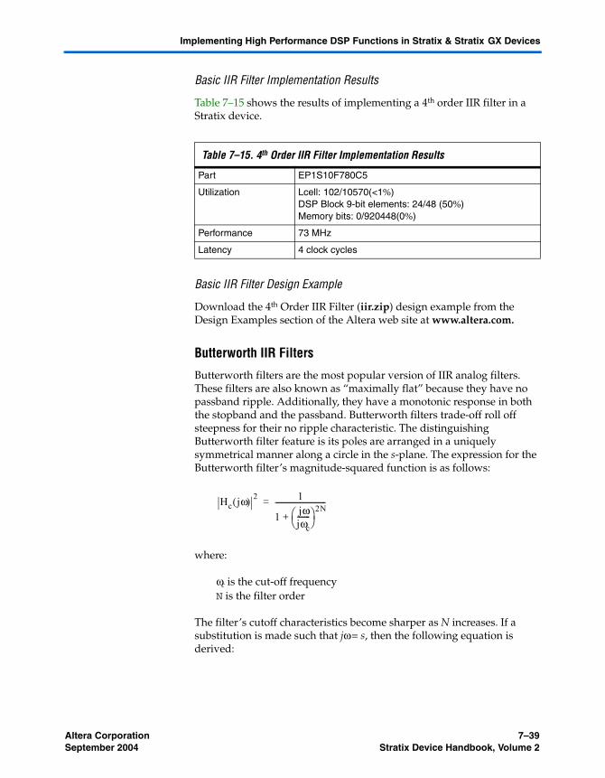
Table 7–15 shows the results of implementing a 4th order IIR filter in a Stratix device.
Basic IIR Filter Design Example
Download the 4th Order IIR Filter (iir.zip) design example from the Design Examples section of the Altera web site at www.altera.com.
Butterworth IIR Filters
Butterworth filters are the most popular version of IIR analog filters. These filters are also known as “maximally flat” because they have no passband ripple. Additionally, they have a monotonic response in both the stopband and the passband. Butterworth filters trade-off roll off steepness for their no ripple characteristic. The distinguishing Butterworth filter feature is its poles are arranged in a uniquely symmetrical manner along a circle in the s-plane. The expression for the Butterworth filter’s magnitude-squared function is as follows:
where:
ωc is the cut-off frequencyN is the filter order
The filter’s cutoff characteristics become sharper as N increases. If a substitution is made such that jω = s, then the following equation is derived:
Table 7–15. 4th Order IIR Filter Implementation Results
Part EP1S10F780C5
Utilization Lcell: 102/10570(<1%)DSP Block 9-bit elements: 24/48 (50%)Memory bits: 0/920448(0%)
Performance 73 MHz
Latency 4 clock cycles
Hc jω( ) 2 1
1 jωjωc-------⎝ ⎠
⎛ ⎞ 2N+
----------------------------=

7–40 Altera CorporationStratix Device Handbook, Volume 2 September 2004
Infinite Impulse Response (IIR) Filters
with poles at:
for k=0,1,…,2N-1
There are 2N poles on the circle with a radius of ωc in the s-plane. These poles are evenly spaced at π/N intervals along the circle. The poles chosen for the implementation of the filter lie in the left half of the s-plane, because these generate a stable, causal filter.
Each of the impulse invariance, the bilinear, and matched z transforms can transform the Laplace transform of the Butterworth filter into the z-transform.
■ Impulse invariance transforms take the inverse of the Laplace transform to obtain the impulse response, then perform a z-transform on the sampled impulse response. The impulse invariance method can cause some aliasing.
■ The bilinear transform maps the entire jω-axis in the s-plane to one revolution of the unit circle in the z-plane. This is the most popular method because it inherently eliminates aliasing.
■ The matched z-transform maps the poles and the zeros of the filter directly from the s-plane to the z-plane. Usually, these transforms are transparent to the user because several tools, such as MATLAB, exist for determining the coefficients of the filter. The z-transform generates the coefficients much like in the basic IIR filter discussed earlier.
Butterworth Filter Implementation
For digital designs, consideration must be made to optimize the IIR biquad structure so that it maps optimally into logic. Because speed is often a critical requirement, the goal is to reduce the number of operations per biquad. It is possible to reduce the number of multipliers needed in each biquad to just two.
Hc s( )Hc s–( ) 1
1 sjωc-------⎝ ⎠
⎛ ⎞ 2N+
----------------------------=
sk 1–( )1
2N-------
jωc( )=
ωce
jπ2N-------⎝ ⎠
⎛ ⎞ 2k N 1–+( )=

Altera Corporation 7–41September 2004 Stratix Device Handbook, Volume 2
Implementing High Performance DSP Functions in Stratix & Stratix GX Devices
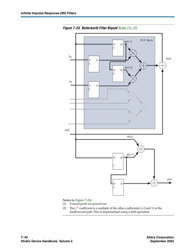
Through the use of integer feedforward multiplies, which can be implemented by combining addition, shifting, and complimenting operations, a Butterworth filter’s transfer function biquad can be optimized for logic synthesis. The most efficient transformation is that of an all pole filter. This is because there is a unique relationship between the feedforward integer coefficients of the filter represented as:
As can be seen by this equation, the z-1 coefficient in the numerator (representing the feedforward path) is twice the other two operands (z-2 and 1). This is always the case in the transformation from the frequency to the digital domain. This represents the normalized response, which is faster and smaller to implement in hardware than real multipliers. It introduces a scaling factor as well, but this can be corrected at the end of the cascade chain through a single multiply.
Figure 7–24 shows how a Butterworth filter biquad is implemented in a Stratix or Stratix GX device.
H z( ) 1 2z 1– z 2–+ +
1 b1z 1– b2z 2–+ +
-------------------------------------------=
7–42 Altera CorporationStratix Device Handbook, Volume 2 September 2004
Infinite Impulse Response (IIR) Filters
Figure 7–24. Butterworth Filter Biquad Notes (1), (2)
Notes to Figure 7–24:(1) Unused ports are grayed out.
(2) The z-1 coefficient is a multiple of the other coefficients (z-2 and 1) in the feedforward path. This is implemented using a shift operation.
w(n-1)
w(n-2)
b1
b2
w(n)
w(n-1)
y(n)
x(n)
DSP block
w(n)D Q
D Q
Altera Corporation 7–43September 2004 Stratix Device Handbook, Volume 2
Implementing High Performance DSP Functions in Stratix & Stratix GX Devices
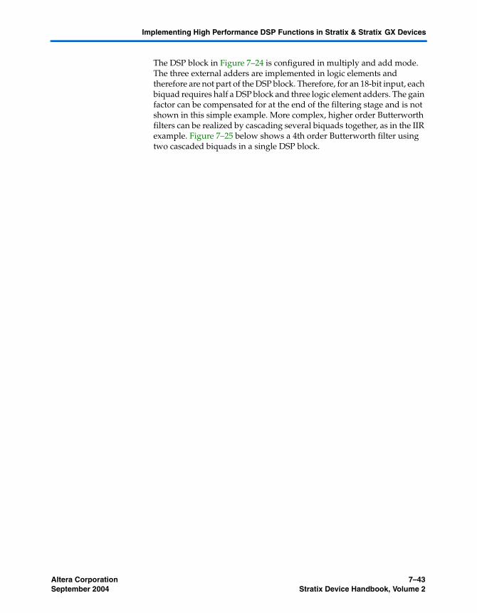
The DSP block in Figure 7–24 is configured in multiply and add mode. The three external adders are implemented in logic elements and therefore are not part of the DSP block. Therefore, for an 18-bit input, each biquad requires half a DSP block and three logic element adders. The gain factor can be compensated for at the end of the filtering stage and is not shown in this simple example. More complex, higher order Butterworth filters can be realized by cascading several biquads together, as in the IIR example. Figure 7–25 below shows a 4th order Butterworth filter using two cascaded biquads in a single DSP block.
7–44 Altera CorporationStratix Device Handbook, Volume 2 September 2004
Infinite Impulse Response (IIR) Filters
Figure 7–25. Cascaded Butterworth Biquads Note (1)
Note to Figure 7–25:(1) The gain factor is compensated for at the end of the filtering stage and is not shown in this figure.
D Q
D Q
D Q
D Q
w1(n-1)
b11
w1(n-2)
b12
D Q
D Q
w2(n-1)
b21
w2(n-2)
b22
w1(n)
w1(n-2)
DSPblock
w2(n)
D Q
D Qw2(n-2)
w2(n-1)
y(n)
x(n)
w1(n-1)
Second biquad
First biquad
D Q
D Q
D Q
D Q

Altera Corporation 7–45September 2004 Stratix Device Handbook, Volume 2
Implementing High Performance DSP Functions in Stratix & Stratix GX Devices
Butterworth Filter Implementation Results
Table 7–16 shows the results of implementing a 4th order Butterworth filter as shown in Figure 7–25.
Butterworth Filter Design Example
Download the 4th Order Butterworth Filter (butterworth.zip) design example from the Design Examples section of the Altera web site at www.altera.com.
Matrix Manipulation
DSP relies heavily on matrix manipulation. The key idea is to transform the digital signals into a format that can then be manipulated mathematically.
This section describes an example of matrix manipulation used in 2-D convolution filter, and its implementation in a Stratix device.
Background on Matrix Manipulation
A matrix can represent all digital signals. Apart from the convenience of compact notation, matrix representation also exploits the benefits of linear algebra. As with one-dimensional, discrete sequences, this advantage becomes more apparent when processing multi-dimensional signals.
In image processing, matrix manipulation is important because it requires analysis in the spatial domain. Smoothing, trend reduction, and sharpening are examples of common image processing operations, which are performed by convolution. This can also be viewed as a digital filter operation with the matrix of filter coefficients forming a convolutional kernel, or mask.
Table 7–16. 4th Order Butterworth Filter Implementation Results
Part EP1S10F780C6
Utilization Lcell: 251/10570(2%)DSP Block 9-bit elements: 16/48 (33%)Memory bits: 0/920448 (0%)
Performance 80 MHz
Latency 4 clock cycles

7–46 Altera CorporationStratix Device Handbook, Volume 2 September 2004
Matrix Manipulation
Two-Dimensional Filtering & Video Imaging
FIR filtering for video applications and image processing in general is used in many applications, including noise removal, image sharpening to feature extraction.
For noise removal, the goal is to reduce the effects of undesirable, contaminative signals that have been linearly added to the image. Applying a low pass filter or smoothing function flattens the image by reducing the rapid pixel-to-pixel variation in gray levels and, ultimately, removing noise. It also has a blurring effect usually used as a precursor for removing unwanted details before extracting certain features from the image.
Image sharpening focuses on the fine details of the image and enhances sharp transitions between the pixels. This acts as a high-pass filter that reduces broad features like the uniform background in an image and enhances compact features or details that have been blurred.
Feature extraction is a form of image analysis slightly different from image processing. The goal of image analysis in general is to extract information based on certain characteristics from the image. This is a multiple step process that includes edge detection. The easiest form of edge detection is the derivative filter, using gradient operators.
All of the operations above involve transformation of the input image. This can be presented as the convolution of the two-dimensional input image, x(m,n) with the impulse response of the transform, f(k,l), resulting in y(m,n) which is the output image.
The f(k,l) function refers to the matrix of filter coefficients. Because the matrix operation is analogous to a filter operation, the matrix itself is considered the impulse response of the filter. Depending on the type of operation, the choice of the convolutional kernel or mask, f(k,l) is different. Figure 7–26 shows an example of convolving a 3 × 3 mask with a larger image.
y m n,( ) f k l,( ) x m n,( )⊗=
y m n,( ) f k l,( )x m k n l–,–( )
l N–=
N
∑k N–=
N
∑=

Altera Corporation 7–47September 2004 Stratix Device Handbook, Volume 2
Implementing High Performance DSP Functions in Stratix & Stratix GX Devices
Figure 7–26. Convolution Using a 3 × 3 Kernel
The output pixel value, y(m,n) depends on the surrounding pixel values in the input image, as well as the filter weights:
To complete the transformation, the kernel slides across the entire image. For pixels on the edge of the image, the convolution operation does not have a complete set of input data. To work around this problem, the pixels on the edge can be left unchanged. In some cases, it is acceptable to have an output image of reduced size. Alternatively, the matrix effect can be applied to edge pixels as if they are surrounded on the “empty” side by
y m n,( ) w1x m 1 n 1–,–( ) w2x m 1 n,–( ) w3x m 1 n 1+,–( )+ +=
+ w4x m n 1–,( ) w5x m n,( ) w6x m n 1+,( )+ +
+ w7x m 1+ n 1–,( ) w8x m 1 n,+( ) w9x m 1 n 1+,+( )+ +
7–48 Altera CorporationStratix Device Handbook, Volume 2 September 2004
Matrix Manipulation
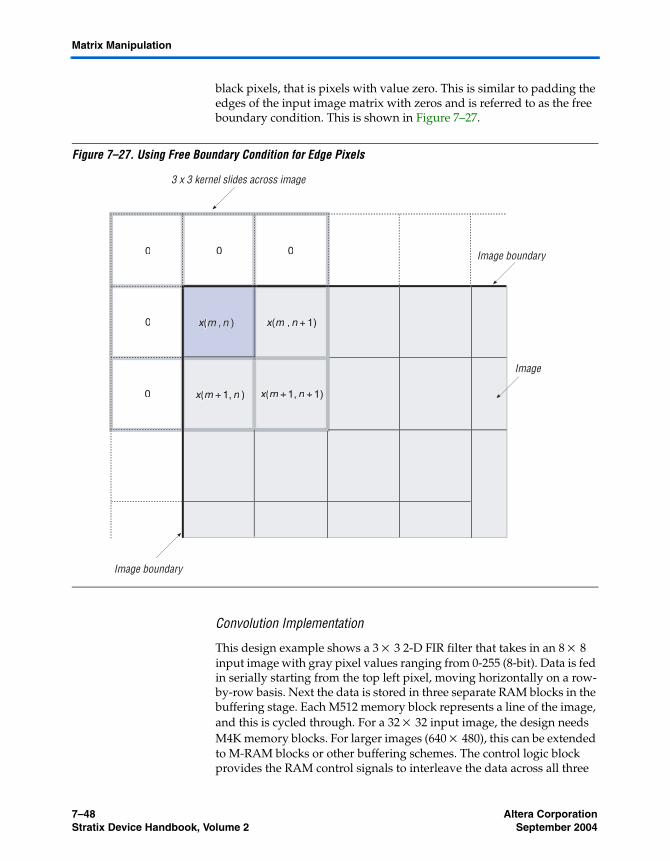
black pixels, that is pixels with value zero. This is similar to padding the edges of the input image matrix with zeros and is referred to as the free boundary condition. This is shown in Figure 7–27.
Figure 7–27. Using Free Boundary Condition for Edge Pixels
Convolution Implementation
This design example shows a 3 × 3 2-D FIR filter that takes in an 8 × 8 input image with gray pixel values ranging from 0-255 (8-bit). Data is fed in serially starting from the top left pixel, moving horizontally on a row-by-row basis. Next the data is stored in three separate RAM blocks in the buffering stage. Each M512 memory block represents a line of the image, and this is cycled through. For a 32 × 32 input image, the design needs M4K memory blocks. For larger images (640 × 480), this can be extended to M-RAM blocks or other buffering schemes. The control logic block provides the RAM control signals to interleave the data across all three
x(xx m +1, n +1)x(xx m +1, n )
x(xx m ,n +1)
0
x(xx
3 x 3 kernel slides across image
0
0
00 Image boundary
Image
Image boundary

Altera Corporation 7–49September 2004 Stratix Device Handbook, Volume 2
Implementing High Performance DSP Functions in Stratix & Stratix GX Devices
RAM blocks. The 9-bit signed filter coefficients feed directly into the filter block. As the data is shifted out from the RAM blocks, the multiplexer block checks for edge pixels and uses the free boundary condition. Figure 7–28 shows a top-level diagram of the design.
Figure 7–28. Block Diagram on Implementation of 3 × 3 Convolutional Filter for an 8 × 8 Pixel Input Image
The 3 × 3 filter block implements the nine multiply-add operations in parallel using two DSP blocks. One DSP block can implement eight of these multipliers. The second DSP block implements the ninth multiplier. The first DSP block is in the four-multipliers adder mode, and the second is in simple multiplier mode. In addition to the two DSP blocks, an external adder is required to sum the output of all nine multipliers. Figure 7–29 shows this implementation.

7–50 Altera CorporationStratix Device Handbook, Volume 2 September 2004
Matrix Manipulation
Figure 7–29. Implementation of 3 × 3 Convolutional Filter Block
DSP Block in Four-Multipliers Adder Mode (9-bit)
LE implemented adder
DSP Block in Simple Multiplier Mode (8-bit)w9
x(m + 1, n + 1)
w8
x(m + 1, n )
w7
x(m + 1, n - 1)
w6
x(m , n + 1)
w5
x(m , n )
w4
x(m , n - 1)
w3
x(m - 1, n + 1)
w2
x(m - 1, n )
w1
x(m - 1, n - 1)
y(m , n )
Note: Unused multipliers and adders grayed out. These multipliers can be used by other functions.
Altera Corporation 7–51September 2004 Stratix Device Handbook, Volume 2
Implementing High Performance DSP Functions in Stratix & Stratix GX Devices
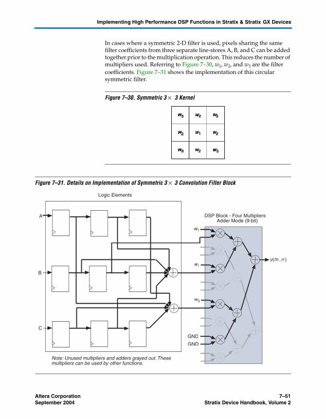
In cases where a symmetric 2-D filter is used, pixels sharing the same filter coefficients from three separate line-stores A, B, and C can be added together prior to the multiplication operation. This reduces the number of multipliers used. Referring to Figure 7–30, w1, w2, and w3 are the filter coefficients. Figure 7–31 shows the implementation of this circular symmetric filter.
Figure 7–30. Symmetric 3 × 3 Kernel
Figure 7–31. Details on Implementation of Symmetric 3 × 3 Convolution Filter Block
DSP Block - Four Multipliers Adder Mode (9-bit)
Logic Elements
GND
w3ww
w2ww
w1
yy(m , n )
GND
A
B
C
Note: Unused multipliers and adders grayed out. These multipliers can be used by other functions.
7–52 Altera CorporationStratix Device Handbook, Volume 2 September 2004
Discrete Cosine Transform (DCT)
Convolution Implementation Results
Table 7–17 shows the results of the 3 × 3 2-D FIR filter implementation in Figure 7–28.
The design requires the input to be an 8 × 8 image, with 8-bit input data and 9-bit filter coefficient width. The output is an image of the same size.
Convolution Design Example
Download the 3 × 3 2-D Convolutional Filter (two_d_fir.zip) design example from the Design Examples section of the Altera web site at www.altera.com.
Discrete Cosine Transform (DCT)
The discrete cosine transform (DCT) is widely used in video and audio compression, for example in JPEG, MPEG video, and MPEG audio. It is a form of transform coding, which is the preferred method for compression techniques. Images tend to compact their energy in the frequency domain making compression in the frequency domain much more effective. This is an important element in compressing data, where the goal is to have a high data compression rate without significant degradation in the image quality.
DCT Background
Similar to the discrete fourier transform (DFT), the DCT is a function that maps the input signal or image from the spatial to the frequency domain. It transforms the input into a linear combination of weighted basis functions. These basis functions are the frequency components of the input data.
Table 7–17. 3 × 3 2-D Convolution Filter Implementation Results
Part EP1S10F780
Utilization Lcell: 372/10570 (3%)DSP block 9-bit elements: 9/48 (18%)Memory bits: 768/920448 (<1%)
Performance 226 MHz
Latency 15 clock cycles

Altera Corporation 7–53September 2004 Stratix Device Handbook, Volume 2
Implementing High Performance DSP Functions in Stratix & Stratix GX Devices
For 1-D with input data x(n) of size N, the DCT coefficients Y(k) are:
for 0 ≤ k ≤ N–1
where:
for k = 0
for 1 ≤ k ≤ N –1
For 2-D with input data x(m,n) of size N × N, the DCT coefficients for the output image, Y(p,q) are:
where:
for p = 0
for q = 0
for 1 ≤ p ≤ N –1
for 1 ≤ q ≤ N–1
2-D DCT Algorithm
The 2-D DCT can be thought of as an extended 1-D DCT applied twice; once in the x direction and again in the y direction. Because the 2-D DCT is a separable transform, it is possible to calculate it using efficient 1-D algorithms. Figure 7–32 illustrates the concept of a separable transform.
Y k( ) α k( )2
----------- x n( ) 2n 1+( )πk2N
---------------------------⎝ ⎠⎛ ⎞cos
n 0=
N 1–
∑=
α k( ) 1N----=
α k( ) 2N----=
Y p q,( ) α p( )α q( )2
----------------------- x m n,( ) 2m 1+( )πp2N
-----------------------------⎝ ⎠⎛ ⎞cos 2n 1+( )πq
2N---------------------------⎝ ⎠
⎛ ⎞cos
n 0=
N 1–
∑m 0=
N 1–
∑=
α p( ) 1N----=
α q( ) 1N----=
α p( ) 2N----=
α q( ) 2N----=

7–54 Altera CorporationStratix Device Handbook, Volume 2 September 2004
Discrete Cosine Transform (DCT)
Figure 7–32. A 2-D DCT is a Separable Transform
This section uses a standard algorithm proposed in [1]. Figure 7–33 shows the flow graph for the algorithm. This is similar to the butterfly computation of the fast fourier transform (FFT). Similar to the FFT algorithms, the DCT algorithm reduces the complexity of the calculation by decomposing the computation into successively smaller DCT components. The even coefficients (y0, y2, y4, y6) are calculated in the upper half and the odd coefficients (y1, y3, y5, y7) in the lower half. As a result of the decomposition, the output is reordered as well.
Figure 7–33. Implementing an N=8 Fast DCT
Stage 1 Stage 4Stage 3Stage 2
x0
x7
x6
x5
x4
x3
x2
x1
y0
y7
y5
y3
y1
y6
y2
y4
yk = cm1s31 + cm2s32 + ... + cmns3n
cx = cos(16
x π)
Multiplied by -1
b
aSum a and b
Multiply-addition block Cm1
yk
S32
S31
Cm2
Cmn
.
.
.
....
S3n
C7
C5
C3
C1
C6
C2 C6
-C2
C4
-C5
-C1
-C7
C3
C3
C7
-C1
C5
-C1
C3
-C5
C7
Stage 3 output (S3)
Matrix coefficent (Cmn)
where
Altera Corporation 7–55September 2004 Stratix Device Handbook, Volume 2
Implementing High Performance DSP Functions in Stratix & Stratix GX Devices
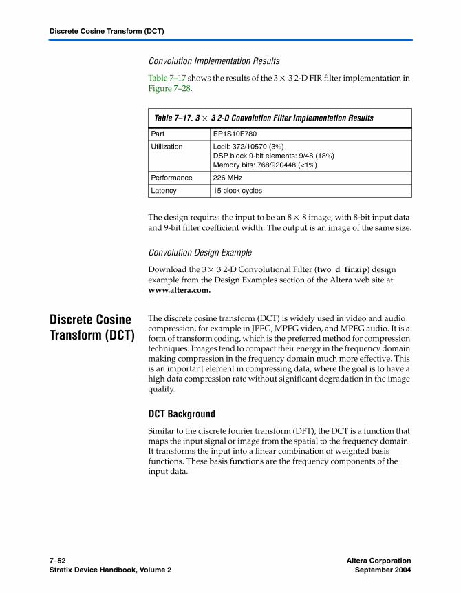
The following defines in matrix format, the 8-point 1-D DCT of Figure 7–33:
where:
[x] is the 1 × 8 input matrix
Y1D x Add1× Add2× Add3 C××=
Add1
1 0 0 0 0 0 0 10 1 0 0 0 0 1 00 0 1 0 0 1 0 00 0 0 1 1 0 0 00 0 0 1 1– 0 0 00 0 1 0 0 1– 0 00 1 0 0 0 0 1– 01 0 0 0 0 0 0 1–
=
Add2
1 0 0 1 0 0 0 00 1 1 0 0 0 0 00 1 1– 0 0 0 0 01 0 0 1– 0 0 0 00 0 0 0 1 0 0 00 0 0 0 0 1 0 00 0 0 0 0 0 1 00 0 0 0 0 0 0 1
=
Add3
1 1 0 0 0 0 0 01 1– 0 0 0 0 0 00 0 1 0 0 0 0 00 0 0 1 0 0 0 00 0 0 0 1 0 0 00 0 0 0 0 1 0 00 0 0 0 0 0 1 00 0 0 0 0 0 0 1
=

7–56 Altera CorporationStratix Device Handbook, Volume 2 September 2004
Discrete Cosine Transform (DCT)
All of the additions in stages 1, 2 and 3 of Figure 7–32 appear in symmetric add and subtract pairs. The entire first stage is simply four such pairs in a very typical cross-over pattern. This pattern is repeated in stages 2 and 3. Multiplication operations are confined to stage 4 in the algorithm. This implementation is shown in more detail in the next section.
DCT Implementation
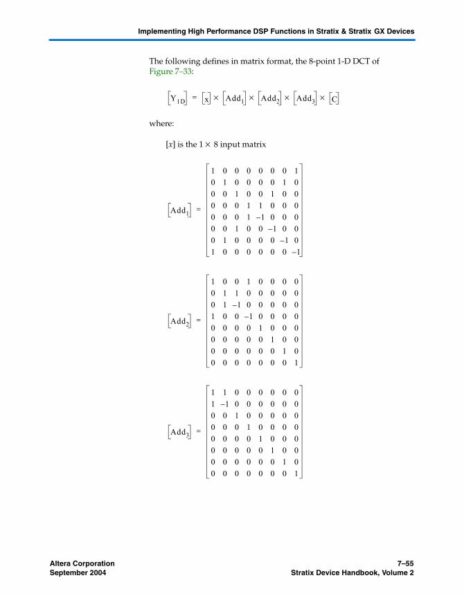
In taking advantage of the separable transform property of the DCT, the implementation can be divided into separate stages; row processing and column processing. However, some data restructuring is necessary before applying the column processing stage to the results from the row processing stage. The data buffering stage must transpose the data first. Figure 7–34 shows the different stages.
Figure 7–34. Three Separate Stages in Implementing the 2-D DCT
Because the row processing and column processing blocks share the same 1-D 8-point DCT algorithm, the hardware implementation shows this block as being shared. The DCT algorithm requires a serial-to-parallel conversion block at the input because it works on blocks of eight data
C
1 0 0 0 0 0 0 00 C4 0 0 0 0 0 0
0 0 C6 C– 2 0 0 0 0
0 0 C2 C6 0 0 0 0
0 0 0 0 C7 C– 5 C3 C– 1
0 0 0 0 C5 C– 1 C7 C3
0 0 0 0 C3 C– 7 C– 1 C– 5
0 0 0 0 C1 C3 C5 C7
=
Cxπx16------cos=
Row processing
Column processing
Transpose matrix
Altera Corporation 7–57September 2004 Stratix Device Handbook, Volume 2
Implementing High Performance DSP Functions in Stratix & Stratix GX Devices
points in parallel. There is also a parallel-to-serial conversion block at the output because the column processing stage generates the output image column-by-column. In order to have the output in the same order as the input (i.e., row-by-row), this conversion is necessary. Appropriate scaling needs to be applied to the completed transform but this can be combined with the quantization stage which often follows a DCT [1]. Figure 7–35 shows a top-level block diagram of this design.
Figure 7–35. Block Diagram on Serial Implementation of 2-D DCT
The implementation of the 1-D DCT block is based on the algorithm shown in Figure 7–33. The simple addition and subtraction operations in stages 1, 2 and 3 are implemented using logic cells. The multiply and multiply-addition operations in stage 4 are implemented using DSP blocks in the Stratix device in the simple multiplier mode, two-multiplier adder mode, and the four-multiplier adder mode. An example of the multiply-addition block is shown in Figure 7–36.

7–58 Altera CorporationStratix Device Handbook, Volume 2 September 2004
Discrete Cosine Transform (DCT)
Figure 7–36. Details on the Implementation of the Multiply-Addition Operation in Stage 4 of the 1-D DCT Algorithm
Note to Figure 7–36:(1) Referring to Figure 7–33. S3n is an output from stage 3 of the DCT and Cmn is a
matrix coefficient. Cx = cos (xπ/16).
DCT Implementation Results
Table 7–18 shows the results of implementing a 2-D DCT with 18-bit precision, as shown in Figure 7–35.
DCT Design Example
Download the 2-D convolutional filter (d_dct.zip) design example from the Design Examples section of the Altera web site at www.altera.com.
Table 7–18. 2-D DCT Implementation Results
Part EP1S20F780
Utilization Lcell: 1717/18460 (9%)DSP Block 9-bit element: 18/80 (22%)Memory bits: 2816/1669248 (<1%)
Performance 165 MHz
Latency 80 clock cycles
DSP Block - Four-Multipliers Adder Mode (18-bit)
Cm1
Cm2
Cm3
Cm4
S31
yk
S34
S33
S32

Altera Corporation 7–59September 2004 Stratix Device Handbook, Volume 2
Implementing High Performance DSP Functions in Stratix & Stratix GX Devices
Arithmetic Functions
Arithmetic functions, such as trigonometric functions, including sine, cosine, magnitude and phase calculation, are important DSP elements. This section discusses the implementation of a simple vector magnitude function in a Stratix device.
Background
Complex numbers can be expressed in two parts: real and imaginary.
where:
a is the real partb is the imaginary partj2= –1
In a two-dimensional plane, a vector (a,b) with reference to the origin (0,0) can also be represented as a complex number. In essence, the x-axis represents the real part, and the y-axis represents the imaginary part (see Figure 7–37).
Figure 7–37. Magnitude of Vector (a,b)
Complex numbers can be converted to phase and amplitude or magnitude representation, using a Cartesian-to-polar coordinate conversion. For a vector (a,b), the phase and magnitude representation is the following:
z a jb+=
7–60 Altera CorporationStratix Device Handbook, Volume 2 September 2004
Arithmetic Functions
Magnitude
Phase angle θ = tan-1(b/a)
This conversion is useful in different applications, such as position control and position monitoring in robotics. It is also important to have these transformations at very high speeds to accommodate real-time processing.
Arithmetic Function Implementation
A common approach to implementing these arithmetic functions is using the coordinate rotation digital computer (CORDIC) algorithm. The CORDIC algorithm calculates the trigonometric functions of sine, cosine, magnitude, and phase using an iterative process. It is made up of a series of micro-rotations of the vector by a set of predetermined constants, which are powers of 2.
Using binary arithmetic, this algorithm essentially replaces multipliers with shift and add operations. In Stratix devices, it is possible to calculate some of these arithmetic functions directly, without having to implement the CORDIC algorithm.
This section describes a design example that calculates the magnitude of a 9-bit signed vector (a,b) using a pipelined version of the square root function available at the Altera IP Megastore. To calculate the sum of the squares of the input (a2 + b2), configure the DSP block in the two-multipliers adder mode. The square root function is implemented using an iterative algorithm similar to the long division operation. The binary numbers are paired off, and subtracted by a trial number. Depending on if the remainder is positive or negative, each bit of the square root is determined and the process is repeated. This square root function does not require memory and is implemented in logic cells only.
In this example, the input bit precision (IN_PREC) feeding into the square root macro is set to twenty, and the output precision (OUT_PREC) is set to ten. The number of precision bits is parameterizable. Also, there is a third parameter, PIPELINE, which controls the architecture of the square root macro. If this parameter is set to YES, it includes pipeline stages in the square root macro. If set to NO, the square root macro becomes a single-cycled combinatorial function.
Figure 7–38 shows the implementation the magnitude design.
m a2 b2+=

Altera Corporation 7–61September 2004 Stratix Device Handbook, Volume 2
Implementing High Performance DSP Functions in Stratix & Stratix GX Devices
Figure 7–38. Implementing the Vector Magnitude Function
DSP Block - Two Multipliers Adder Mode (9-bit)
a
b
Note: Unused multipliers and adders grayed out.
LE implemented square root function
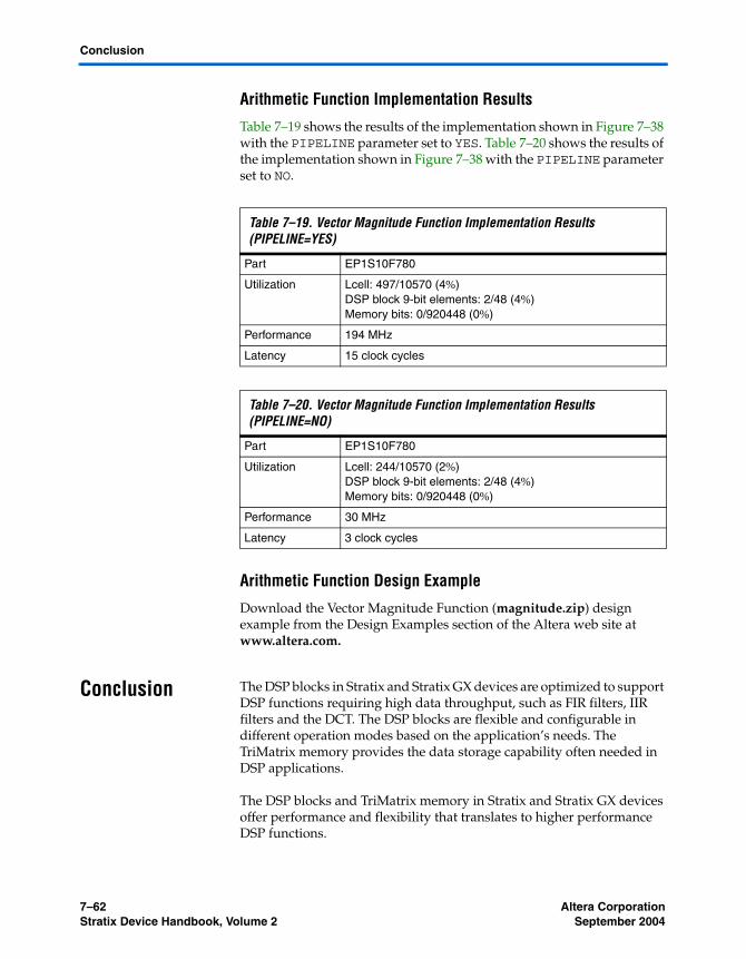
7–62 Altera CorporationStratix Device Handbook, Volume 2 September 2004
Conclusion
Arithmetic Function Implementation Results
Table 7–19 shows the results of the implementation shown in Figure 7–38 with the PIPELINE parameter set to YES. Table 7–20 shows the results of the implementation shown in Figure 7–38 with the PIPELINE parameter set to NO.
Arithmetic Function Design Example
Download the Vector Magnitude Function (magnitude.zip) design example from the Design Examples section of the Altera web site at www.altera.com.
Conclusion The DSP blocks in Stratix and Stratix GX devices are optimized to support DSP functions requiring high data throughput, such as FIR filters, IIR filters and the DCT. The DSP blocks are flexible and configurable in different operation modes based on the application’s needs. The TriMatrix memory provides the data storage capability often needed in DSP applications.
The DSP blocks and TriMatrix memory in Stratix and Stratix GX devices offer performance and flexibility that translates to higher performance DSP functions.
Table 7–19. Vector Magnitude Function Implementation Results (PIPELINE=YES)
Part EP1S10F780
Utilization Lcell: 497/10570 (4%)DSP block 9-bit elements: 2/48 (4%)Memory bits: 0/920448 (0%)
Performance 194 MHz
Latency 15 clock cycles
Table 7–20. Vector Magnitude Function Implementation Results (PIPELINE=NO)
Part EP1S10F780
Utilization Lcell: 244/10570 (2%)DSP block 9-bit elements: 2/48 (4%)Memory bits: 0/920448 (0%)
Performance 30 MHz
Latency 3 clock cycles
Altera Corporation 7–63September 2004 Stratix Device Handbook, Volume 2
Implementing High Performance DSP Functions in Stratix & Stratix GX Devices
References See the following for more information:
■ Optimal DCT for Hardware ImplementationM. Langhammer. Proceedings of International Conference on Signal Processing Applications & Technology (ICSPAT) '95, October 1995
■ Digital Signal Processing: Principles, Algorithms, and ApplicationsJohn G. Proakis, Dimitris G. Manolakis. Prentice Hall
■ Hardware Implementation of Multirate Digital FiltersTony San. Communication Systems Design, April 2000
■ AN 73: Implementing FIR Filters in FLEX Devices
■ Efficient Logic Synthesis Techniques for IIR FiltersM.Langhammer. Proceedings of International Conference on Signal Processing Applications & Technology (ICSPAT) '95, October 1995

7–64 Altera CorporationStratix Device Handbook, Volume 2 September 2004
References