selectable i/o standards in stratix ii and stratix ii gx devices · 2018-06-16 · selectable i/o...
TRANSCRIPT

Altera Corporation January 2008
SII52004-4.6
4. Selectable I/O Standards inStratix II and Stratix II GX
Devices
Introduction This chapter provides guidelines for using industry I/O standards in Stratix® II and Stratix II GX devices, including:
■ I/O features■ I/O standards■ External memory interfaces■ I/O banks■ Design considerations
Stratix II and Stratix II GX I/O Features
Stratix II and the Stratix II GX devices contain an abundance of adaptive logic modules (ALMs), embedded memory, high-bandwidth digital signal processing (DSP) blocks, and extensive routing resources, all of which can operate at very high core speed.
Stratix II and Stratix II GX devices I/O structure is designed to ensure that these internal capabilities are fully utilized. There are numerous I/O features to assist in high-speed data transfer into and out of the device including:
■ Single-ended, non-voltage-referenced and voltage-referenced I/O standards
■ High-speed differential I/O standards featuring serializer/deserializer (SERDES), dynamic phase alignment (DPA), capable of 1 gigabit per second (Gbps) performance for low-voltage differential signaling (LVDS), Hypertransport technology, HSTL, SSTL, and LVPECL
1 HSTL and SSTL I/O standards are used only for PLL clock inputs and outputs in differential mode. LVPECL is supported on clock input and outputs of the top and bottom I/O banks.
■ Double data rate (DDR) I/O pins■ Programmable output drive strength for voltage-referenced and
non-voltage-referenced single-ended I/O standards■ Programmable bus-hold■ Programmable pull-up resistor■ Open-drain output■ On-chip series termination■ On-chip parallel termination
4–1

Stratix II and Stratix II GX I/O Standards Support
■ On-chip differential termination■ Peripheral component interconnect (PCI) clamping diode■ Hot socketing
f For a detailed description of each I/O feature, refer to the Stratix II Architecture chapter in volume 1 of the Stratix II Device Handbook or the Stratix II GX Architecture chapter in volume 1 of the Stratix II GX Device Handbook.
Stratix II and Stratix II GX I/O Standards Support
Stratix II and Stratix II GX devices support a wide range of industry I/O standards. Table 4–1 shows which I/O standards Stratix II devices support as well as typical applications.
Table 4–1. Stratix II and Stratix II GX I/O Standard Applications (Part 1 of 2)
I/O Standard Application
LVTTL General purpose
LVCMOS General purpose
2.5 V General purpose
1.8 V General purpose
1.5 V General purpose
3.3-V PCI PC and embedded system
3.3-V PCI-X PC and embedded system
SSTL-2 Class I DDR SDRAM
SSTL-2 Class II DDR SDRAM
SSTL-18 Class I DDR2 SDRAM
SSTL-18 Class II DDR2 SDRAM
1.8-V HSTL Class I QDRII SRAM/RLDRAM II/SRAM
1.8-V HSTL Class II QDRII SRAM/RLDRAM II/SRAM
1.5-V HSTL Class I QDRII SRAM/SRAM
1.5-V HSTL Class II QDRII SRAM/SRAM
1.2-V HSTL General purpose
Differential SSTL-2 Class I DDR SDRAM
Differential SSTL-2 Class II DDR SDRAM
Differential SSTL-18 Class I DDR2 SDRAM
Differential SSTL-18 Class II DDR2 SDRAM
1.8-V differential HSTL Class I Clock interfaces
1.8-V differential HSTL Class II Clock interfaces
1.5-V differential HSTL Class I Clock interfaces
4–2 Altera CorporationStratix II Device Handbook, Volume 2 January 2008

Selectable I/O Standards in Stratix II and Stratix II GX Devices
Single-Ended I/O Standards
In non-voltage-referenced single-ended I/O standards, the voltage at the input must be above a set voltage to be considered “on” (high, or logic value 1) or below another voltage to be considered “off” (low, or logic value 0). Voltages between the limits are undefined logically, and may fall into either a logic value 0 or 1. The non-voltage-referenced single-ended I/O standards supported by Stratix II and Stratix II GX devices are:
■ Low-voltage transistor-transistor logic (LVTTL)■ Low-voltage complementary metal-oxide semiconductor (LVCMOS)■ 1.5 V■ 1.8 V■ 2.5 V■ 3.3-V PCI■ 3.3-V PCI-X
Voltage-referenced, single-ended I/O standards provide faster data rates. These standards use a constant reference voltage at the input levels. The incoming signals are compared with this constant voltage and the difference between the two defines “on” and “off” states.
1 Stratix II and Stratix II GX devices support stub series terminated logic (SSTL) and high-speed transceiver logic (HSTL) voltage-referenced I/O standards.
LVTTL
The LVTTL standard is formulated under EIA/JEDEC Standard, JESD8-B (Revision of JESD8-A): Interface Standard for Nominal 3-V/3.3-V Supply Digital Integrated Circuits.
The standard defines DC interface parameters for digital circuits operating from a 3.0- or 3.3-V power supply and driving or being driven by LVTTL-compatible devices. The 3.3-V LVTTL standard is a
1.5-V differential HSTL Class II Clock interfaces
LVDS High-speed communications
HyperTransport™ technology PCB interfaces
Differential LVPECL Video graphics and clock distribution
Table 4–1. Stratix II and Stratix II GX I/O Standard Applications (Part 2 of 2)
I/O Standard Application
Altera Corporation 4–3January 2008 Stratix II Device Handbook, Volume 2

Stratix II and Stratix II GX I/O Standards Support
general-purpose, single-ended standard used for 3.3-V applications. This I/O standard does not require input reference voltages (VREF) or termination voltages (VTT).
1 Stratix II and Stratix II GX devices support both input and output levels for 3.3-V LVTTL operation.
Stratix II Stratix II GX devices support a VCCIO voltage level of 3.3 V ± 5% as specified as the narrow range for the voltage supply by the EIA/JEDEC standard.
LVCMOS
The LVCMOS standard is formulated under EIA/JEDEC Standard, JESD8-B (Revision of JESD8-A): Interface Standard for Nominal 3-V/3.3-V Supply Digital Integrated Circuits.
The standard defines DC interface parameters for digital circuits operating from a 3.0- or 3.3-V power supply and driving or being driven by LVCMOS-compatible devices. The 3.3-V LVCMOS I/O standard is a general-purpose, single-ended standard used for 3.3-V applications. While LVCMOS has its own output specification, it specifies the same input voltage requirements as LVTTL. These I/O standards do not require VREF or VTT.
1 Stratix II and Stratix II GX devices support both input and output levels for 3.3-V LVCMOS operation.
Stratix II and Stratix II GX devices support a VCCIO voltage level of 3.3 V ±5% as specified as the narrow range for the voltage supply by the EIA/JEDEC standard.
2.5 V
The 2.5-V I/O standard is formulated under EIA/JEDEC Standard, EIA/JESD8-5: 2.5-V± 0.2-V (Normal Range), and 1.8-V – 2.7-V (Wide Range) Power Supply Voltage and Interface Standard for Non-Terminated Digital Integrated Circuit.
The standard defines the DC interface parameters for high-speed, low-voltage, non-terminated digital circuits driving or being driven by other 2.5-V devices. This standard is a general-purpose, single-ended standard used for 2.5-V applications. It does not require the use of a VREF or a VTT.
4–4 Altera CorporationStratix II Device Handbook, Volume 2 January 2008
Selectable I/O Standards in Stratix II and Stratix II GX Devices
1 Stratix II and Stratix II GX devices support both input and output levels for 2.5-V operation with VCCIO voltage level support of 2.5 V ± 5%, which is narrower than defined in the Normal Range of the EIA/JEDEC standard.
1.8 V
The 1.8-V I/O standard is formulated under EIA/JEDEC Standard, EIA/JESD8-7: 1.8-V± 0.15-V (Normal Range), and 1.2-V – 1.95-V (Wide Range) Power Supply Voltage and Interface Standard for Non-Terminated Digital Integrated Circuit.
The standard defines the DC interface parameters for high-speed, low-voltage, non-terminated digital circuits driving or being driven by other 1.8-V devices. This standard is a general-purpose, single-ended standard used for 1.8-V applications. It does not require the use of a VREF or a VTT.
1 Stratix II and Stratix II GX devices support both input and output levels for 1.8-V operation with VCCIO voltage level support of 1.8 V ± 5%, which is narrower than defined in the Normal Range of the EIA/JEDEC standard.
1.5 V
The 1.5-V I/O standard is formulated under EIA/JEDEC Standard, JESD8-11: 1.5-V± 0.1-V (Normal Range) and 0.9-V – 1.6-V (Wide Range) Power Supply Voltage and Interface Standard for Non-Terminated Digital Integrated Circuit.
The standard defines the DC interface parameters for high-speed, low-voltage, non-terminated digital circuits driving or being driven by other 1.5-V devices. This standard is a general-purpose, single-ended standard used for 1.5-V applications. It does not require the use of a VREF or a VTT.
1 Stratix II and Stratix II GX devices support both input and output levels for 1.5-V operation VCCIO voltage level support of 1.5 V ± 5%, which is narrower than defined in the Normal Range of the EIA/JEDEC standard.
3.3-V PCI
The 3.3-V PCI I/O standard is formulated under PCI Local Bus Specification Revision 2.2 developed by the PCI Special Interest Group (SIG).
Altera Corporation 4–5January 2008 Stratix II Device Handbook, Volume 2

Stratix II and Stratix II GX I/O Standards Support
The PCI local bus specification is used for applications that interface to the PCI local bus, which provides a processor-independent data path between highly integrated peripheral controller components, peripheral add-in boards, and processor/memory systems. The conventional PCI specification revision 2.2 defines the PCI hardware environment including the protocol, electrical, mechanical, and configuration specifications for the PCI devices and expansion boards. This standard requires 3.3-V VCCIO. Stratix II and Stratix II GX devices are fully compliant with the 3.3-V PCI Local Bus Specification Revision 2.2 and meet 64-bit/66-MHz operating frequency and timing requirements.
1 The 3.3-V PCI standard does not require input reference voltages or board terminations. Stratix II and Stratix II GX devices support both input and output levels.
3.3-V PCI-X
The 3.3-V PCI-X I/O standard is formulated under PCI-X Local Bus Specification Revision 1.0a developed by the PCI SIG.
The PCI-X 1.0 standard is used for applications that interface to the PCI local bus. The standard enables the design of systems and devices that operate at clock speeds up to 133 MHz, or 1 Gbps for a 64-bit bus. The PCI-X 1.0 protocol enhancements enable devices to operate much more efficiently, providing more usable bandwidth at any clock frequency. By using the PCI-X 1.0 standard, you can design devices to meet PCI-X 1.0 requirements and operate as conventional 33- and 66-MHz PCI devices when installed in those systems. This standard requires 3.3-V VCCIO. Stratix II and Stratix II GX devices are fully compliant with the 3.3-V PCI-X Specification Revision 1.0a and meet the 133-MHz operating frequency and timing requirements. The 3.3-V PCI-X standard does not require input reference voltages or board terminations.
1 Stratix II and Stratix II GX devices support both input and output levels operation.
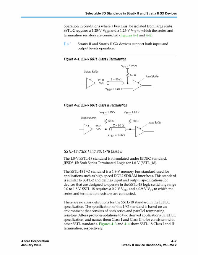
SSTL-2 Class I and SSTL-2 Class II
The 2.5-V SSTL-2 standard is formulated under JEDEC Standard, JESD8-9A: Stub Series Terminated Logic for 2.5-V (SSTL_2).
The SSTL-2 I/O standard is a 2.5-V memory bus standard used for applications such as high-speed DDR SDRAM interfaces. This standard defines the input and output specifications for devices that operate in the SSTL-2 logic switching range of 0.0 to 2.5 V. This standard improves
4–6 Altera CorporationStratix II Device Handbook, Volume 2 January 2008
Selectable I/O Standards in Stratix II and Stratix II GX Devices
operation in conditions where a bus must be isolated from large stubs. SSTL-2 requires a 1.25-V VREF and a 1.25-V VTT to which the series and termination resistors are connected (Figures 4–1 and 4–2).
1 Stratix II and Stratix II GX devices support both input and output levels operation.
Figure 4–1. 2.5-V SSTL Class I Termination
Figure 4–2. 2.5-V SSTL Class II Termination
SSTL-18 Class I and SSTL-18 Class II
The 1.8-V SSTL-18 standard is formulated under JEDEC Standard, JESD8-15: Stub Series Terminated Logic for 1.8-V (SSTL_18).
The SSTL-18 I/O standard is a 1.8-V memory bus standard used for applications such as high-speed DDR2 SDRAM interfaces. This standard is similar to SSTL-2 and defines input and output specifications for devices that are designed to operate in the SSTL-18 logic switching range 0.0 to 1.8 V. SSTL-18 requires a 0.9-V VREF and a 0.9-V VTT to which the series and termination resistors are connected.
There are no class definitions for the SSTL-18 standard in the JEDEC specification. The specification of this I/O standard is based on an environment that consists of both series and parallel terminating resistors. Altera provides solutions to two derived applications in JEDEC specification, and names them Class I and Class II to be consistent with other SSTL standards. Figures 4–3 and 4–4 show SSTL-18 Class I and II termination, respectively.
Output Buffer
Input Buffer
VTT = 1.25 V
50 Ω
25 Ω Z = 50 Ω
VREF = 1.25 V
Output Buffer
Input Buffer
VTT = 1.25 V
50 Ω
VTT = 1.25 V
50 Ω
25 Ω Z = 50 Ω
VREF = 1.25 V
Altera Corporation 4–7January 2008 Stratix II Device Handbook, Volume 2

Stratix II and Stratix II GX I/O Standards Support
1 Stratix II and Stratix II GX devices support both input and output levels operation.
Figure 4–3. 1.8-V SSTL Class I Termination
Figure 4–4. 1.8-V SSTL Class II Termination
1.8-V HSTL Class I and 1.8-V HSTL Class II
The HSTL standard is a technology-independent I/O standard developed by JEDEC to provide voltage scalability. It is used for applications designed to operate in the 0.0- to 1.8-V HSTL logic switching range such as quad data rate (QDR) memory clock interfaces.
Although JEDEC specifies a maximum VCCIO value of 1.6 V, there are various memory chip vendors with HSTL standards that require a VCCIO of 1.8 V. Stratix II and Stratix II GX devices support interfaces to chips with VCCIO of 1.8 V for HSTL. Figures 4–5 and 4–6 show the nominal VREF and VTT required to track the higher value of VCCIO. The value of VREF is selected to provide optimum noise margin in the system.
1 Stratix II and Stratix II GX devices support both input and output levels operation.
Output Buffer
Input Buffer
VTT = 0.9 V
50 Ω
25 Ω Z = 50 Ω
VREF = 0.9 V
Output Buffer
Input Buffer
VTT = 0.9 V
50 Ω
VTT = 0.9 V
50 Ω
25 Ω Z = 50 Ω
VREF = 0.9 V
4–8 Altera CorporationStratix II Device Handbook, Volume 2 January 2008

Selectable I/O Standards in Stratix II and Stratix II GX Devices
Figure 4–5. 1.8-V HSTL Class I Termination
Figure 4–6. 1.8-V HSTL Class II Termination
1.5-V HSTL Class I and 1.5-V HSTL Class II
The 1.5-V HSTL standard is formulated under EIA/JEDEC Standard, EIA/JESD8-6: A 1.5-V Output Buffer Supply Voltage Based Interface Standard for Digital Integrated Circuits.
The 1.5-V HSTL I/O standard is used for applications designed to operate in the 0.0- to 1.5-V HSTL logic nominal switching range. This standard defines single-ended input and output specifications for all HSTL-compliant digital integrated circuits. The 1.5-V HSTL I/O standard in Stratix II and Stratix II GX devices are compatible with the 1.8-V HSTL I/O standard in APEX™ 20KE, APEX 20KC, and in Stratix II and Stratix II GX devices themselves because the input and output voltage thresholds are compatible (Figures 4–7 and 4–8).
1 Stratix II and Stratix II GX devices support both input and output levels with VREF and VTT.
Output Buffer
Input Buffer
VTT = 0.9 V
50 ΩZ = 50 Ω
VREF = 0.9 V
Output Buffer
Input Buffer
VTT = 0.9 V
50 ΩZ = 50 Ω
VREF = 0.9 V
VTT = 0.9 V
50 Ω
Altera Corporation 4–9January 2008 Stratix II Device Handbook, Volume 2

Stratix II and Stratix II GX I/O Standards Support
Figure 4–7. 1.5-V HSTL Class I Termination
Figure 4–8. 1.5-V HSTL Class II Termination
1.2-V HSTL
Although there is no EIA/JEDEC standard available for the 1.2-V HSTL standard, Altera supports it for applications that operate in the 0.0 to 1.2-V HSTL logic nominal switching range. 1.2-V HSTL can be terminated through series or parallel on-chip termination (OCT). Figure 4–9 shows the termination scheme.
Figure 4–9. 1.2-V HSTL Termination
Differential I/O Standards
Differential I/O standards are used to achieve even faster data rates with higher noise immunity. Apart from LVDS, LVPECL, and HyperTransport technology, Stratix II and Stratix II GX devices also support differential versions of SSTL and HSTL standards.
Output Buffer
Input Buffer
VTT = 0.75 V
50 ΩZ = 50 Ω
VREF = 0.75 V
Output Buffer
Input Buffer
VTT = 0.75 V
50 Ω
VTT = 0.75 V
50 ΩZ = 50 Ω
VREF = 0.75 V
Output Buffer
Input BufferZ = 50 Ω
VREF = 0.6 V
OCT
4–10 Altera CorporationStratix II Device Handbook, Volume 2 January 2008

Selectable I/O Standards in Stratix II and Stratix II GX Devices
f For detailed information on differential I/O standards, refer to the High-Speed Differential I/O Interfaces with DPA in Stratix II & Stratix II GX Devices chapter in volume 2 of the Stratix II Device Handbook or High-Speed Differential I/O Interfaces with DPA in Stratix II & Stratix II GX Devices chapter in volume 2 of the Stratix II GX Device Handbook.
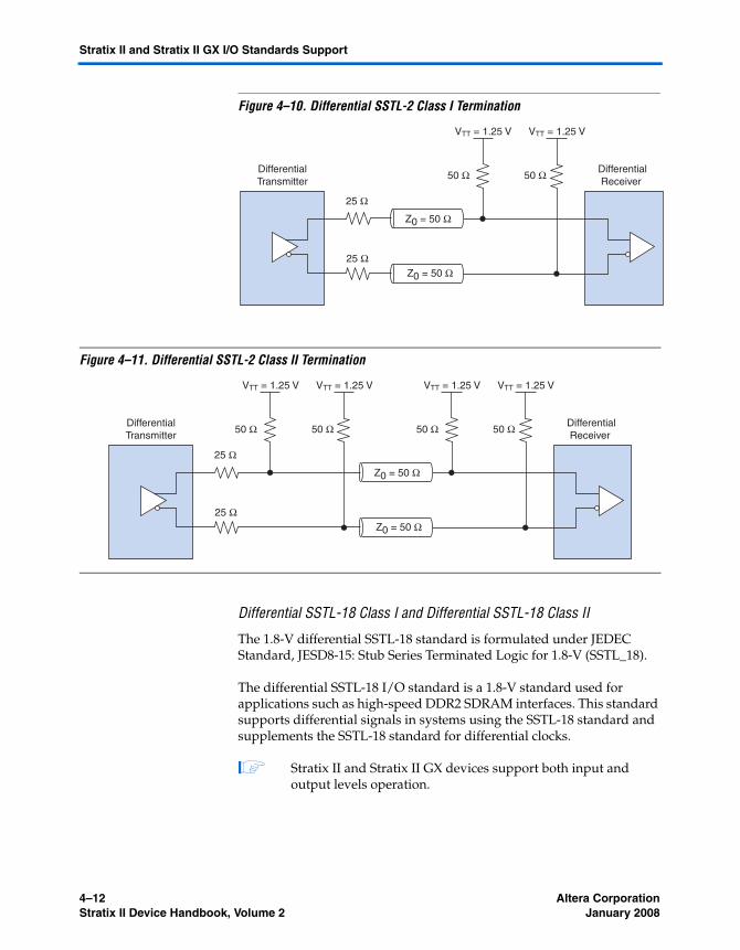
Differential SSTL-2 Class I and Differential SSTL-2 Class II
The 2.5-V differential SSTL-2 standard is formulated under JEDEC Standard, JESD8-9A: Stub Series Terminated Logic for 2.5-V (SSTL_2).
This I/O standard is a 2.5-V standard used for applications such as high-speed DDR SDRAM clock interfaces. This standard supports differential signals in systems using the SSTL-2 standard and supplements the SSTL-2 standard for differential clocks. Stratix II and Stratix II GX devices support both input and output levels. Figures 4–10 and 4–11 shows details on differential SSTL-2 termination.
1 Stratix II and Stratix II GX devices support differential SSTL-2 I/O standards in pseudo-differential mode, which is implemented by using two SSTL-2 single-ended buffers.
The Quartus® II software only supports pseudo-differential standards on the INCLK, FBIN and EXTCLK ports of enhanced PLL, as well as on DQS pins when DQS megafunction (ALTDQS, Bidirectional Data Strobe) is used. Two single-ended output buffers are automatically programmed to have opposite polarity so as to implement a pseudo-differential output. A proper VREF voltage is required for the two single-ended input buffers to implement a pseudo-differential input. In this case, only the positive polarity input is used in the speed path while the negative input is not connected internally. In other words, only the non-inverted pin is required to be specified in your design, while the Quartus II software automatically generates the inverted pin for you.
Although the Quartus II software does not support pseudo-differential SSTL-2 I/O standards on the left and right I/O banks, you can implement these standards at these banks. You need to create two pins in the designs and configure the pins with single-ended SSTL-2 standards. However, this is limited only to pins that support the differential pin-pair I/O function and is dependent on the single-ended SSTL-2 standards support at these banks.
Altera Corporation 4–11January 2008 Stratix II Device Handbook, Volume 2
Stratix II and Stratix II GX I/O Standards Support
Figure 4–10. Differential SSTL-2 Class I Termination
Figure 4–11. Differential SSTL-2 Class II Termination
Differential SSTL-18 Class I and Differential SSTL-18 Class II
The 1.8-V differential SSTL-18 standard is formulated under JEDEC Standard, JESD8-15: Stub Series Terminated Logic for 1.8-V (SSTL_18).
The differential SSTL-18 I/O standard is a 1.8-V standard used for applications such as high-speed DDR2 SDRAM interfaces. This standard supports differential signals in systems using the SSTL-18 standard and supplements the SSTL-18 standard for differential clocks.
1 Stratix II and Stratix II GX devices support both input and output levels operation.
DifferentialTransmitter
DifferentialReceiver
Z0 = 50 Ω
50 Ω 50 Ω
Z0 = 50 Ω
VTT = 1.25 V VTT = 1.25 V
25 Ω
25 Ω
DifferentialTransmitter
DifferentialReceiver
Z0 = 50 Ω
50 Ω 50 Ω
Z0 = 50 Ω
VTT = 1.25 V VTT = 1.25 V
50 Ω 50 Ω
VTT = 1.25 V VTT = 1.25 V
25 Ω
25 Ω
4–12 Altera CorporationStratix II Device Handbook, Volume 2 January 2008

Selectable I/O Standards in Stratix II and Stratix II GX Devices
Figures 4–12 and 4–13 shows details on differential SSTL-18 termination. Stratix II and Stratix II GX devices support differential SSTL-18 I/O standards in pseudo-differential mode, which is implemented by using two SSTL-18 single-ended buffers.
The Quartus II software only supports pseudo-differential standards on the INCLK, FBIN and EXTCLK ports of enhanced PLL, as well as on DQS pins when DQS megafunction (ALTDQS, Bidirectional Data Strobe) is used. Two single-ended output buffers are automatically programmed to have opposite polarity so as to implement a pseudo-differential output. A proper VREF voltage is required for the two single-ended input buffers to implement a pseudo-differential input. In this case, only the positive polarity input is used in the speed path while the negative input is not connected internally. In other words, only the non-inverted pin is required to be specified in your design, while the Quartus II software automatically generates the inverted pin for you.
Although the Quartus II software does not support pseudo-differential SSTL-18 I/O standards on the left and right I/O banks, you can implement these standards at these banks. You need to create two pins in the designs and configure the pins with single-ended SSTL-18 standards. However, this is limited only to pins that support the differential pin-pair I/O function and is dependent on the single-ended SSTL-18 standards support at these banks.
Figure 4–12. Differential SSTL-18 Class I Termination
DifferentialTransmitter
DifferentialReceiver
Z0 = 50 Ω
50 Ω 50 Ω
Z0 = 50 Ω
VTT = 0.9 V VTT = 0.9 V
25 Ω
25 Ω
Altera Corporation 4–13January 2008 Stratix II Device Handbook, Volume 2

Stratix II and Stratix II GX I/O Standards Support
Figure 4–13. Differential SSTL-18 Class II Termination
1.8-V Differential HSTL Class I and 1.8-V Differential HSTL Class II
The 1.8-V differential HSTL specification is the same as the 1.8-V single-ended HSTL specification. It is used for applications designed to operate in the 0.0- to 1.8-V HSTL logic switching range such as QDR memory clock interfaces. Stratix II and Stratix II GX devices support both input and output levels operation. Figures 4–14 and 4–15 show details on 1.8-V differential HSTL termination.
Stratix II and Stratix II GX devices support 1.8-V differential HSTL I/O standards in pseudo-differential mode, which is implemented by using two 1.8-V HSTL single-ended buffers.
The Quartus II software only supports pseudo-differential standards on the INCLK, FBIN and EXTCLK ports of enhanced PLL, as well as on DQS pins when DQS megafunction (ALTDQS, Bidirectional Data Strobe) is used. Two single-ended output buffers are automatically programmed to have opposite polarity so as to implement a pseudo-differential output. A proper VREF voltage is required for the two single-ended input buffers to implement a pseudo-differential input. In this case, only the positive polarity input is used in the speed path while the negative input is not connected internally. In other words, only the non-inverted pin is required to be specified in your design, while the Quartus II software automatically generates the inverted pin for you.
Although the Quartus II software does not support 1.8-V pseudo-differential HSTL I/O standards on left/right I/O banks, you can implement these standards at these banks. You need to create two pins in the designs and configure the pins with single-ended 1.8-V HSTL standards. However, this is limited only to pins that support the differential pin-pair I/O function and is dependent on the single-ended 1.8-V HSTL standards support at these banks.
DifferentialTransmitter
DifferentialReceiver
Z0 = 50 Ω
50 Ω 50 Ω
Z0 = 50 Ω
VTT = 0.9 V VTT = 0.9 V
50 Ω 50 Ω
VTT = 0.9 V VTT = 0.9 V
25 Ω
25 Ω
4–14 Altera CorporationStratix II Device Handbook, Volume 2 January 2008

Selectable I/O Standards in Stratix II and Stratix II GX Devices
Figure 4–14. 1.8-V Differential HSTL Class I Termination
Figure 4–15. 1.8-V Differential HSTL Class II Termination
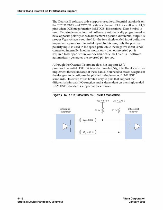
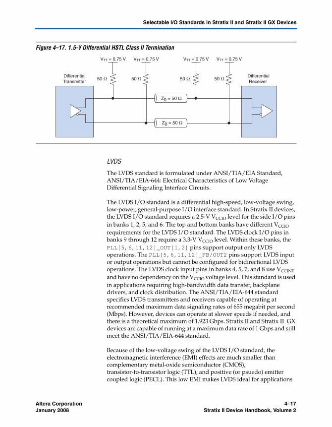
1.5-V Differential HSTL Class I and 1.5-V Differential HSTL Class II
The 1.5-V differential HSTL standard is formulated under EIA/JEDEC Standard, EIA/JESD8-6: A 1.5-V Output Buffer Supply Voltage Based Interface Standard for Digital Integrated Circuits.
The 1.5-V differential HSTL specification is the same as the 1.5-V single-ended HSTL specification. It is used for applications designed to operate in the 0.0- to 1.5-V HSTL logic switching range, such as QDR memory clock interfaces. Stratix II and Stratix II GX devices support both input and output levels operation. Figures 4–16 and 4–17 show details on the 1.5-V differential HSTL termination.
Stratix II and Stratix II GX devices support 1.5-V differential HSTL I/O standards in pseudo-differential mode, which is implemented by using two 1.5-V HSTL single-ended buffers.
DifferentialTransmitter
DifferentialReceiver
Z0 = 50 Ω
50 Ω 50 Ω
Z0 = 50 Ω
VTT = 0.9 V VTT = 0.9 V
DifferentialTransmitter
DifferentialReceiver
Z0 = 50 Ω
50 Ω 50 Ω
Z0 = 50 Ω
VTT = 0.9 V VTT = 0.9 V
50 Ω 50 Ω
VTT = 0.9 V VTT = 0.9 V
Altera Corporation 4–15January 2008 Stratix II Device Handbook, Volume 2
Stratix II and Stratix II GX I/O Standards Support
The Quartus II software only supports pseudo-differential standards on the INCLK, FBIN and EXTCLK ports of enhanced PLL, as well as on DQS pins when DQS megafunction (ALTDQS, Bidirectional Data Strobe) is used. Two single-ended output buffers are automatically programmed to have opposite polarity so as to implement a pseudo-differential output. A proper VREF voltage is required for the two single-ended input buffers to implement a pseudo-differential input. In this case, only the positive polarity input is used in the speed path while the negative input is not connected internally. In other words, only the non-inverted pin is required to be specified in your design, while the Quartus II software automatically generates the inverted pin for you.
Although the Quartus II software does not support 1.5-V pseudo-differential HSTL I/O standards on left/right I/O banks, you can implement these standards at these banks. You need to create two pins in the designs and configure the pins with single-ended 1.5-V HSTL standards. However, this is limited only to pins that support the differential pin-pair I/O function and is dependent on the single-ended 1.8-V HSTL standards support at these banks.
Figure 4–16. 1.5-V Differential HSTL Class I Termination
DifferentialTransmitter
DifferentialReceiver
Z0 = 50 Ω
50 Ω 50 Ω
Z0 = 50 Ω
VTT = 0.75 V VTT = 0.75 V
4–16 Altera CorporationStratix II Device Handbook, Volume 2 January 2008
Selectable I/O Standards in Stratix II and Stratix II GX Devices
Figure 4–17. 1.5-V Differential HSTL Class II Termination
LVDS
The LVDS standard is formulated under ANSI/TIA/EIA Standard, ANSI/TIA/EIA-644: Electrical Characteristics of Low Voltage Differential Signaling Interface Circuits.
The LVDS I/O standard is a differential high-speed, low-voltage swing, low-power, general-purpose I/O interface standard. In Stratix II devices, the LVDS I/O standard requires a 2.5-V VCCIO level for the side I/O pins in banks 1, 2, 5, and 6. The top and bottom banks have different VCCIO requirements for the LVDS I/O standard. The LVDS clock I/O pins in banks 9 through 12 require a 3.3-V VCCIO level. Within these banks, the PLL[5,6,11,12]_OUT[1,2] pins support output only LVDS operations. The PLL[5,6,11,12]_FB/OUT2 pins support LVDS input or output operations but cannot be configured for bidirectional LVDS operations. The LVDS clock input pins in banks 4, 5, 7, and 8 use VCCINT and have no dependency on the VCCIO voltage level. This standard is used in applications requiring high-bandwidth data transfer, backplane drivers, and clock distribution. The ANSI/TIA/EIA-644 standard specifies LVDS transmitters and receivers capable of operating at recommended maximum data signaling rates of 655 megabit per second (Mbps). However, devices can operate at slower speeds if needed, and there is a theoretical maximum of 1.923 Gbps. Stratix II and Stratix II GX devices are capable of running at a maximum data rate of 1 Gbps and still meet the ANSI/TIA/EIA-644 standard.
Because of the low-voltage swing of the LVDS I/O standard, the electromagnetic interference (EMI) effects are much smaller than complementary metal-oxide semiconductor (CMOS), transistor-to-transistor logic (TTL), and positive (or psuedo) emitter coupled logic (PECL). This low EMI makes LVDS ideal for applications
DifferentialTransmitter
DifferentialReceiver
Z0 = 50 Ω
50 Ω 50 Ω
Z0 = 50 Ω
VTT = 0.75 V VTT = 0.75 V
50 Ω 50 Ω
VTT = 0.75 V VTT = 0.75 V
Altera Corporation 4–17January 2008 Stratix II Device Handbook, Volume 2

Stratix II and Stratix II GX I/O Standards Support
with low EMI requirements or noise immunity requirements. The LVDS standard does not require an input reference voltage. However, it does require a 100-Ω termination resistor between the two signals at the input buffer. Stratix II and Stratix II GX devices provide an optional 100-Ω differential LVDS termination resistor in the device using on-chip differential termination. Stratix II and Stratix II GX devices support both input and output levels operation.
Differential LVPECL
The low-voltage positive (or pseudo) emitter coupled logic (LVPECL) standard is a differential interface standard requiring a 3.3-V VCCIO. The standard is used in applications involving video graphics, telecommunications, data communications, and clock distribution. The high-speed, low-voltage swing LVPECL I/O standard uses a positive power supply and is similar to LVDS. However, LVPECL has a larger differential output voltage swing than LVDS. The LVPECL standard does not require an input reference voltage, but it does require a 100-Ω termination resistor between the two signals at the input buffer. Figures 4–18 and 4–19 show two alternate termination schemes for LVPECL.
1 Stratix II and Stratix II GX devices support both input and output levels operation.
Figure 4–18. LVPECL DC Coupled Termination
Figure 4–19. LVPECL AC Coupled Termination
Output Buffer Input Buffer
100 Ω
Z = 50 Ω
Z = 50 Ω
Output Buffer
Input Buffer
100 Ω
Z = 50 Ω
Z = 50 Ω
VCCIO
VCCIO
R2 R2
R1 R110 to 100 nF
10 to 100 nF
4–18 Altera CorporationStratix II Device Handbook, Volume 2 January 2008
Selectable I/O Standards in Stratix II and Stratix II GX Devices
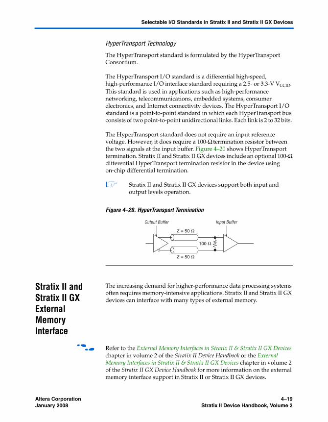
HyperTransport Technology
The HyperTransport standard is formulated by the HyperTransport Consortium.
The HyperTransport I/O standard is a differential high-speed, high-performance I/O interface standard requiring a 2.5- or 3.3-V VCCIO. This standard is used in applications such as high-performance networking, telecommunications, embedded systems, consumer electronics, and Internet connectivity devices. The HyperTransport I/O standard is a point-to-point standard in which each HyperTransport bus consists of two point-to-point unidirectional links. Each link is 2 to 32 bits.
The HyperTransport standard does not require an input reference voltage. However, it does require a 100-Ω termination resistor between the two signals at the input buffer. Figure 4–20 shows HyperTransport termination. Stratix II and Stratix II GX devices include an optional 100-Ω differential HyperTransport termination resistor in the device using on-chip differential termination.
1 Stratix II and Stratix II GX devices support both input and output levels operation.
Figure 4–20. HyperTransport Termination
Stratix II and Stratix II GX External Memory Interface
The increasing demand for higher-performance data processing systems often requires memory-intensive applications. Stratix II and Stratix II GX devices can interface with many types of external memory.
f Refer to the External Memory Interfaces in Stratix II & Stratix II GX Devices chapter in volume 2 of the Stratix II Device Handbook or the External Memory Interfaces in Stratix II & Stratix II GX Devices chapter in volume 2 of the Stratix II GX Device Handbook for more information on the external memory interface support in Stratix II or Stratix II GX devices.
Output Buffer Input Buffer
100 Ω
Z = 50 Ω
Z = 50 Ω
Altera Corporation 4–19January 2008 Stratix II Device Handbook, Volume 2

Stratix II and Stratix II GX I/O Banks
Stratix II and Stratix II GX I/O Banks
Stratix II devices have eight general I/O banks and four enhanced phase-locked loop (PLL) external clock output banks (Figure 4–21). I/O banks 1, 2, 5, and 6 are on the left or right sides of the device and I/O banks 3, 4, and 7 through 12 are at the top or bottom of the device.
Figure 4–21. Stratix II I/O Banks Notes (1), (2), (3), (4), (5), (6), (7)
Notes to Figure 4–21:(1) Figure 4–21 is a top view of the silicon die that corresponds to a reverse view for flip-chip packages. It is a graphical
representation only. Refer to the pin list and Quartus II software for exact locations.(2) Depending on the size of the device, different device members have different numbers of VREF groups.(3) Banks 9 through 12 are enhanced PLL external clock output banks. These PLL banks utilize the adjacent VREF group
when voltage-referenced standards are implemented. For example, if an SSTL input is implemented in PLL bank 10, the voltage level at VREFB7 is the reference voltage level for the SSTL input.
(4) Differential HSTL and differential SSTL standards are available for bidirectional operations on DQS pin and input-only operations on PLL clock input pins; LVDS, LVPECL, and HyperTransport standards are available for input-only operations on PLL clock input pins. Refer to the “Differential I/O Standards” on page 4–10 for more details.
(5) Quartus II software does not support differential SSTL and differential HSTL standards at left/right I/O banks. Refer to the “Differential I/O Standards” on page 4–10 if you need to implement these standards at these I/O banks.
(6) Banks 11 and 12 are available only in EP2S60, EP2S90, EP2S130, and EP2S180 devices.(7) PLLs 7, 8, 9 10, 11, and 12 are available only in EP2S60, EP2S90, EP2S130, and EP2S180 devices.
Bank 3 Bank 4Bank 11 Bank 9
PLL11 PLL5
PLL7
PLL1
PLL2
PLL4
PLL3
PLL10
I/O banks 7, 8, 10 & 12 support all
single-ended I/O standards and
differential I/O standards except for
HyperTransport technology for
both input and output operations.
I/O banks 3, 4, 9 & 11 support all
single-ended I/O standards and
differential I/O standards except for
HyperTransport technology for
both input and output operations.
VREF0B3 VREF1B3 VREF2B3 VREF3B3 VREF4B3 VREF0B4 VREF1B4 VREF2B4 VREF3B4 VREF4B4
Bank 8 Bank 7Bank 12 Bank 10
PLL12 PLL6
PLL8 PLL9VREF4B8 VREF3B8 VREF2B8 VREF1B8 VREF0B8 VREF4B7 VREF3B7 VREF2B7 VREF1B7 VREF0B7
VR
EF
3B
2V
RE
F2
B2
VR
EF
1B
2V
RE
F0
B2
Ba
nk 2
VR
EF
3B
1V
RE
F2
B1
VR
EF
1B
1V
RE
F0
B1
Ban
k 1
VR
EF
1B
5V
RE
F2
B5
VR
EF
3B
5V
RE
F4
B5
Ba
nk 5
VR
EF
1B
6V
RE
F2
B6
VR
EF
3B
6V
RE
F4
B6
Ban
k 6
VR
EF
4B
2
VR
EF
0B
5
VR
EF
4B
1
VR
EF
0B
6
DQS4T DQS3T DQS2T DQS1T DQS0T
DQS4B DQS3B DQS2B DQS1B DQS0BDQS8B DQS7B DQS6B DQS5B
DQS8T DQS7T DQS6T DQS5T
This I/O bank supports LVDS
and LVPECL standards for input
clock operations. Differential
HSTL and differential SSTL
standards are supported for both
input and output operations.
This I/O bank supports LVDS
and LVPECL standards for input
clock operations. Differential
HSTL and differential SSTL
standards are supported for both
input and output operations.
This I/O bank supports LVDS
and LVPECL standards for input
clock operations. Differential
HSTL and differential SSTL
standards are supported for both
input and output operations.
This I/O bank supports LVDS
and LVPECL standards for input
clock operations. Differential
HSTL and differential SSTL
standards are supported for both
input and output operations.
I/O banks 1, 2, 5 & 6 support LVTTL, LVCMOS,
2.5-V, 1.8-V, 1.5-V, SSTL-2, SSTL-18 Class I,
HSTL-18 Class I, HSTL-15 Class I, LVDS, and
HyperTransport standards for input and output
operations. HSTL-18 Class II, HSTL-15-Class II,
SSTL-18 Class II standards are only supported
for input operations.
4–20 Altera CorporationStratix II Device Handbook, Volume 2 January 2008
Selectable I/O Standards in Stratix II and Stratix II GX Devices
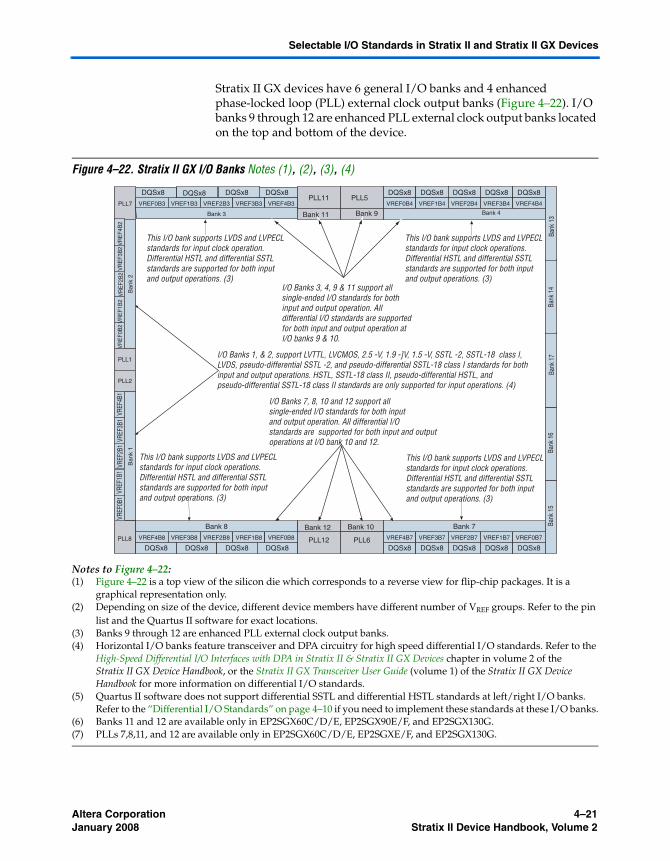
Stratix II GX devices have 6 general I/O banks and 4 enhanced phase-locked loop (PLL) external clock output banks (Figure 4–22). I/O banks 9 through 12 are enhanced PLL external clock output banks located on the top and bottom of the device.
Figure 4–22. Stratix II GX I/O Banks Notes (1), (2), (3), (4)
Notes to Figure 4–22:(1) Figure 4–22 is a top view of the silicon die which corresponds to a reverse view for flip-chip packages. It is a
graphical representation only.(2) Depending on size of the device, different device members have different number of VREF groups. Refer to the pin
list and the Quartus II software for exact locations.(3) Banks 9 through 12 are enhanced PLL external clock output banks.(4) Horizontal I/O banks feature transceiver and DPA circuitry for high speed differential I/O standards. Refer to the
High-Speed Differential I/O Interfaces with DPA in Stratix II & Stratix II GX Devices chapter in volume 2 of the Stratix II GX Device Handbook, or the Stratix II GX Transceiver User Guide (volume 1) of the Stratix II GX Device Handbook for more information on differential I/O standards.
(5) Quartus II software does not support differential SSTL and differential HSTL standards at left/right I/O banks. Refer to the “Differential I/O Standards” on page 4–10 if you need to implement these standards at these I/O banks.
(6) Banks 11 and 12 are available only in EP2SGX60C/D/E, EP2SGX90E/F, and EP2SGX130G.(7) PLLs 7,8,11, and 12 are available only in EP2SGX60C/D/E, EP2SGXE/F, and EP2SGX130G.
I/O Banks 3, 4, 9 & 11 support all single-ended I/O standards for both input and output operation. All differential I/O standards are supported for both input and output operation at I/O banks 9 & 10.
I/O Banks 7, 8, 10 and 12 support all single-ended I/O standards for both input and output operation. All differential I/O standards are supported for both input and output operations at I/O bank 10 and 12.
I/O Banks 1, & 2, support LVTTL, LVCMOS, 2.5 -V, 1.9 -]V, 1.5 -V, SSTL -2, SSTL-18 class I, LVDS, pseudo-differential SSTL -2, and pseudo-differential SSTL-18 class I standards for both input and output operations. HSTL, SSTL-18 class II, pseudo-differential HSTL, and pseudo-differential SSTL-18 class II standards are only supported for input operations. (4)
DQSx8 DQSx8 DQSx8 DQSx8 DQSx8PLL11
VREF0B3 VREF1B3 VREF2B3 VREF3B3 VREF4B3 VREF0B4 VREF1B4 VREF2B4 VREF3B4 VREF4B4
VREF4B8 VREF3B8 VREF2B8 VREF1B8 VREF0B8 VREF4B7 VREF3B7 VREF2B7 VREF1B7 VREF0B7
DQSx8 DQSx8 DQSx8 DQSx8 DQSx8 DQSx8 DQSx8 DQSx8 DQSx8
Bank 9Bank 11
VR
EF0
B2
VR
EF1
B2
VR
EF2
B2
PLL1
PLL2
Ban
k 1
Ban
k 2
Bank 3 Bank 4
Bank 8 Bank 7
PLL7
PLL8 PLL12
PLL5
This I/O bank supports LVDS and LVPECLstandards for input clock operations. Differential HSTL and differential SSTL standards are supported for both input and output operations. (3)
This I/O bank supports LVDS and LVPECLstandards for input clock operation. Differential HSTL and differential SSTL standards are supported for both input and output operations. (3)
This I/O bank supports LVDS and LVPECLstandards for input clock operations. Differential HSTL and differential SSTL standards are supported for both input and output operations. (3)
This I/O bank supports LVDS and LVPECLstandards for input clock operations. Differential HSTL and differential SSTL standards are supported for both input and output operations. (3)
PLL6
Bank 12 Bank 10
VREF
0B1
VREF
1B1
VREF
2B1
VREF
3B1
VREF
4B1
Bank
15
Bank
16
Bank
14
Bank
13
Bank
17
DQSx8DQSx8DQSx8DQSx8
VR
EF4
B2
VR
EF3
B2
Altera Corporation 4–21January 2008 Stratix II Device Handbook, Volume 2

Stratix II and Stratix II GX I/O Banks
Programmable I/O Standards
Stratix II and Stratix II GX device programmable I/O standards deliver high-speed and high-performance solutions in many complex design systems. This section discusses the I/O standard support in the I/O banks of Stratix II and Stratix II GX devices.
Regular I/O Pins
Most Stratix II and Stratix II GX device pins are multi-function pins. These pins support regular inputs and outputs as their primary function, and offer an optional function such as DQS, differential pin-pair, or PLL external clock outputs. For example, you can configure a multi-function pin in the enhanced PLL external clock output bank as a PLL external clock output when it is not used as a regular I/O pin.
1 I/O pins that reside in PLL banks 9 through 12 are powered by the VCC_PLL<5, 6, 11, or 12>_OUT pins, respectively. The EP2S60F484, EP2S60F780, EP2S90H484, EP2S90F780, and EP2S130F780 devices do not support PLLs 11 and 12. Therefore, any I/O pins that reside in bank 11 are powered by the VCCIO3 pin, and any I/O pins that reside in bank 12 are powered by the VCCIO8 pin.
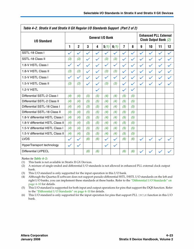
Table 4–2 shows the I/O standards supported when a pin is used as a regular I/O pin in the I/O banks of Stratix II and Stratix II GX devices.
Table 4–2. Stratix II and Stratix II GX Regular I/O Standards Support (Part 1 of 2)
I/O StandardGeneral I/O Bank Enhanced PLL External
Clock Output Bank (2)
1 2 3 4 5(1) 6(1) 7 8 9 10 11 12
LVTTL v v v v v v v v v v v v
LVCMOS v v v v v v v v v v v v
2.5 V v v v v v v v v v v v v
1.8 V v v v v v v v v v v v v
1.5 V v v v v v v v v v v v v
3.3-V PCI v v v v v v v v
3.3-V PCI-X v v v v v v v v
SSTL-2 Class I v v v v v v v v v v v v
SSTL-2 Class II v v v v v v v v v v v v
4–22 Altera CorporationStratix II Device Handbook, Volume 2 January 2008
Selectable I/O Standards in Stratix II and Stratix II GX Devices
SSTL-18 Class I v v v v v v v v v v v v
SSTL-18 Class II (3) (3) v v (3) (3) v v v v v v
1.8-V HSTL Class I v v v v v v v v v v v v
1.8-V HSTL Class II (3) (3) v v (3) (3) v v v v v v
1.5-V HSTL Class I v v v v v v v v v v v v
1.5-V HSTL Class II (3) (3) v v (3) (3) v v v v v v
1.2-V HSTL v v v
Differential SSTL-2 Class I (4) (4) (5) (5) (4) (4) (5) (5)
Differential SSTL-2 Class II (4) (4) (5) (5) (4) (4) (5) (5)
Differential SSTL-18 Class I (4) (4) (5) (5) (4) (4) (5) (5)
Differential SSTL-18 Class II (4) (4) (5) (5) (4) (4) (5) (5)
1.8-V differential HSTL Class I (4) (4) (5) (5) (4) (4) (5) (5)
1.8-V differential HSTL Class II (4) (4) (5) (5) (4) (4) (5) (5)
1.5-V differential HSTL Class I (4) (4) (5) (5) (4) (4) (5) (5)
1.5-V differential HSTL Class II (4) (4) (5) (5) (4) (4) (5) (5)
LVDS v v (6) (6) v v (6) (6) v v v v
HyperTransport technology v v v v
Differential LVPECL (6) (6) (6) (6) v v v v
Notes to Table 4–2:(1) This bank is not available in Stratix II GX Devices.(2) A mixture of single-ended and differential I/O standards is not allowed in enhanced PLL external clock output
bank.(3) This I/O standard is only supported for the input operation in this I/O bank.(4) Although the Quartus II software does not support pseudo-differential SSTL/HSTL I/O standards on the left and
right I/O banks, you can implement these standards at these banks. Refer to the “Differential I/O Standards” on page 4–10 for details.
(5) This I/O standard is supported for both input and output operations for pins that support the DQS function. Refer to the “Differential I/O Standards” on page 4–10 for details.
(6) This I/O standard is only supported for the input operation for pins that support PLL INCLK function in this I/O bank.
Table 4–2. Stratix II and Stratix II GX Regular I/O Standards Support (Part 2 of 2)
I/O StandardGeneral I/O Bank Enhanced PLL External
Clock Output Bank (2)
1 2 3 4 5(1) 6(1) 7 8 9 10 11 12
Altera Corporation 4–23January 2008 Stratix II Device Handbook, Volume 2

Stratix II and Stratix II GX I/O Banks
Clock I/O Pins
The PLL clock I/O pins consist of clock inputs (INCLK), external feedback inputs (FBIN), and external clock outputs (EXTCLK). Clock inputs are located at the left and right I/O banks (banks 1, 2, 5, and 6) to support fast PLLs, and at the top and bottom I/O banks (banks 3, 4, 7, and 8) to support enhanced PLLs. Both external clock outputs and external feedback inputs are located at enhanced PLL external clock output banks (banks 9, 10, 11, and 12) to support enhanced PLLs. Table 4–3 shows the PLL clock I/O support in the I/O banks of Stratix II and Stratix II GX devices.
Table 4–3. I/O Standards Supported for Stratix II and Stratix II GX PLL Pins (Part 1 of 2)
I/O Standard (2)
Enhanced PLL (1) Fast PLL
Input Output Input
INCLK FBIN EXTCLK INCLK
LVTTL v v v v
LVCMOS v v v v
2.5 V v v v v
1.8 V v v v v
1.5 V v v v v
3.3-V PCI v v v
3.3-V PCI-X v v v
SSTL-2 Class I v v v v
SSTL-2 Class II v v v v
SSTL-18 Class I v v v v
SSTL-18 Class II v v v v
1.8-V HSTL Class I v v v v
1.8-V HSTL Class II v v v v
1.5-V HSTL Class I v v v v
1.5-V HSTL Class II v v v v
Differential SSTL-2 Class I v v v
Differential SSTL-2 Class II v v v
Differential SSTL-18 Class I v v v
Differential SSTL-18 Class II v v v
4–24 Altera CorporationStratix II Device Handbook, Volume 2 January 2008

Selectable I/O Standards in Stratix II and Stratix II GX Devices
f For more information, refer to the PLLs in Stratix II & Stratix II GX Devices chapter in volume 2 of the Stratix II Device Handbook or the PLLs in Stratix II & Straix II GX Devices chapter in volume 2 of the Stratix II GX Device Handbook.
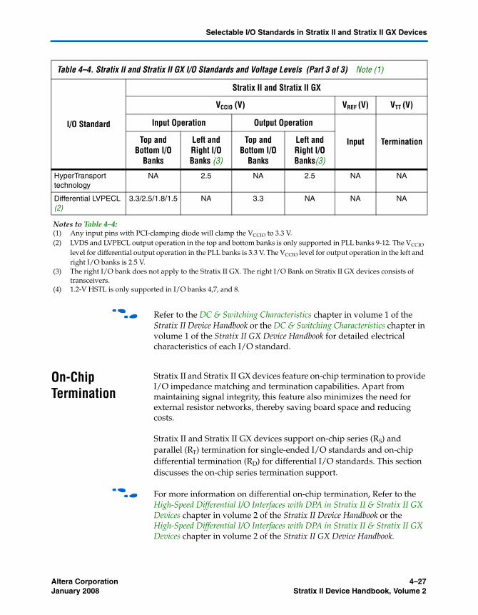
Voltage Levels
Stratix II device specify a range of allowed voltage levels for supported I/O standards. Table 4–4 shows only typical values for input and output VCCIO, VREF, as well as the board VTT.
1.8-V differential HSTL Class I v v v
1.8-V differential HSTL Class II v v v
1.5-V differential HSTL Class I v v v
1.5-V differential HSTL Class II v v v
LVDS v v v v
HyperTransport technology v
Differential LVPECL v v v
Note to Table 4–3:(1) The enhanced PLL external clock output bank does not allow a mixture of both single-ended and differential I/O
standards.(2) Altera does not support 1.2-V HSTL for PLL input pins on column I/O pins.
Table 4–3. I/O Standards Supported for Stratix II and Stratix II GX PLL Pins (Part 2 of 2)
I/O Standard (2)
Enhanced PLL (1) Fast PLL
Input Output Input
INCLK FBIN EXTCLK INCLK
Table 4–4. Stratix II and Stratix II GX I/O Standards and Voltage Levels (Part 1 of 3) Note (1)
I/O Standard
Stratix II and Stratix II GX
VCCIO (V) VREF (V) VTT (V)
Input Operation Output Operation
Input TerminationTop andBottom I/O
Banks
Left and Right I/O Banks (3)
Top and Bottom I/O
Banks
Left and Right I/O Banks(3)
LVTTL 3.3/2.5 3.3/2.5 3.3 3.3 NA NA
LVCMOS 3.3/2.5 3.3/2.5 3.3 3.3 NA NA
Altera Corporation 4–25January 2008 Stratix II Device Handbook, Volume 2

Stratix II and Stratix II GX I/O Banks
2.5 V 3.3/2.5 3.3/2.5 2.5 2.5 NA NA
1.8 V 1.8/1.5 1.8/1.5 1.8 1.8 NA NA
1.5 V 1.8/1.5 1.8/1.5 1.5 1.5 NA NA
3.3-V PCI 3.3 NA 3.3 NA NA NA
3.3-V PCI-X 3.3 NA 3.3 NA NA NA
SSTL-2 Class I 2.5 2.5 2.5 2.5 1.25 1.25
SSTL-2 Class II 2.5 2.5 2.5 2.5 1.25 1.25
SSTL-18 Class I 1.8 1.8 1.8 1.8 0.90 0.90
SSTL-18 Class II 1.8 1.8 1.8 NA 0.90 0.90
1.8-V HSTL Class I 1.8 1.8 1.8 1.8 0.90 0.90
1.8-V HSTL Class II 1.8 1.8 1.8 NA 0.90 0.90
1.5-V HSTL Class I 1.5 1.5 1.5 1.5 0.75 0.75
1.5-V HSTL Class II 1.5 1.5 1.5 NA 0.75 0.75
1.2-V HSTL(4) 1.2 NA 1.2 NA 0.6 NA
Differential SSTL-2 Class I
2.5 2.5 2.5 2.5 1.25 1.25
Differential SSTL-2 Class II
2.5 2.5 2.5 2.5 1.25 1.25
Differential SSTL-18 Class I
1.8 1.8 1.8 1.8 0.90 0.90
Differential SSTL-18 Class II
1.8 1.8 1.8 NA 0.90 0.90
1.8-V differential HSTL Class I
1.8 1.8 1.8 NA 0.90 0.90
1.8-V differential HSTL Class II
1.8 1.8 1.8 NA 0.90 0.90
1.5-V differential HSTL Class I
1.5 1.5 1.5 NA 0.75 0.75
1.5-V differential HSTL Class II
1.5 1.5 1.5 NA 0.75 0.75
LVDS (2) 3.3/2.5/1.8/1.5 2.5 3.3 2.5 NA NA
Table 4–4. Stratix II and Stratix II GX I/O Standards and Voltage Levels (Part 2 of 3) Note (1)
I/O Standard
Stratix II and Stratix II GX
VCCIO (V) VREF (V) VTT (V)
Input Operation Output Operation
Input TerminationTop andBottom I/O
Banks
Left and Right I/O Banks (3)
Top and Bottom I/O
Banks
Left and Right I/O Banks(3)
4–26 Altera CorporationStratix II Device Handbook, Volume 2 January 2008
Selectable I/O Standards in Stratix II and Stratix II GX Devices
f Refer to the DC & Switching Characteristics chapter in volume 1 of the Stratix II Device Handbook or the DC & Switching Characteristics chapter in volume 1 of the Stratix II GX Device Handbook for detailed electrical characteristics of each I/O standard.
On-Chip Termination
Stratix II and Stratix II GX devices feature on-chip termination to provide I/O impedance matching and termination capabilities. Apart from maintaining signal integrity, this feature also minimizes the need for external resistor networks, thereby saving board space and reducing costs.
Stratix II and Stratix II GX devices support on-chip series (RS) and parallel (RT) termination for single-ended I/O standards and on-chip differential termination (RD) for differential I/O standards. This section discusses the on-chip series termination support.
f For more information on differential on-chip termination, Refer to the High-Speed Differential I/O Interfaces with DPA in Stratix II & Stratix II GX Devices chapter in volume 2 of the Stratix II Device Handbook or the High-Speed Differential I/O Interfaces with DPA in Stratix II & Stratix II GX Devices chapter in volume 2 of the Stratix II GX Device Handbook.
HyperTransport technology
NA 2.5 NA 2.5 NA NA
Differential LVPECL (2)
3.3/2.5/1.8/1.5 NA 3.3 NA NA NA
Notes to Table 4–4:(1) Any input pins with PCI-clamping diode will clamp the VCCIO to 3.3 V.(2) LVDS and LVPECL output operation in the top and bottom banks is only supported in PLL banks 9-12. The VCCIO
level for differential output operation in the PLL banks is 3.3 V. The VCCIO level for output operation in the left and right I/O banks is 2.5 V.
(3) The right I/O bank does not apply to the Stratix II GX. The right I/O Bank on Stratix II GX devices consists of transceivers.
(4) 1.2-V HSTL is only supported in I/O banks 4,7, and 8.
Table 4–4. Stratix II and Stratix II GX I/O Standards and Voltage Levels (Part 3 of 3) Note (1)
I/O Standard
Stratix II and Stratix II GX
VCCIO (V) VREF (V) VTT (V)
Input Operation Output Operation
Input TerminationTop andBottom I/O
Banks
Left and Right I/O Banks (3)
Top and Bottom I/O
Banks
Left and Right I/O Banks(3)
Altera Corporation 4–27January 2008 Stratix II Device Handbook, Volume 2

On-Chip Termination
The Stratix II and Stratix II GX devices supports I/O driver on-chip series (RS) and parallel (RT) termination through drive strength control for single-ended I/Os. There are three ways to implement the RS and (RT) in Stratix II and Stratix II GX devices:
■ RS without calibration for both row I/Os and column I/Os■ RS with calibration only for column I/Os■ RT with calibration only for column I/Os
On-Chip Series Termination without Calibration
Stratix II and Stratix II GX devices support driver impedance matching to provide the I/O driver with controlled output impedance that closely matches the impedance of the transmission line. As a result, reflections can be significantly reduced. Stratix II and Stratix II GX devices support on-chip series termination for single-ended I/O standards (see Figure 4–23). The RS shown in Figure 4–23 is the intrinsic impedance of transistors. The typical RS values are 25Ω and 50Ω. Once matching impedance is selected, current drive strength is no longer selectable.
1 On-chip series termination without calibration is supported on output pins or on the output function of bidirectional pins.
Figure 4–23. Stratix II and Stratix II GX On-Chip Series Termination without Calibration
Stratix II DriverSeries Impedance
ReceivingDevice
VCCIO
RS
RS
ZO
GND
4–28 Altera CorporationStratix II Device Handbook, Volume 2 January 2008
Selectable I/O Standards in Stratix II and Stratix II GX Devices
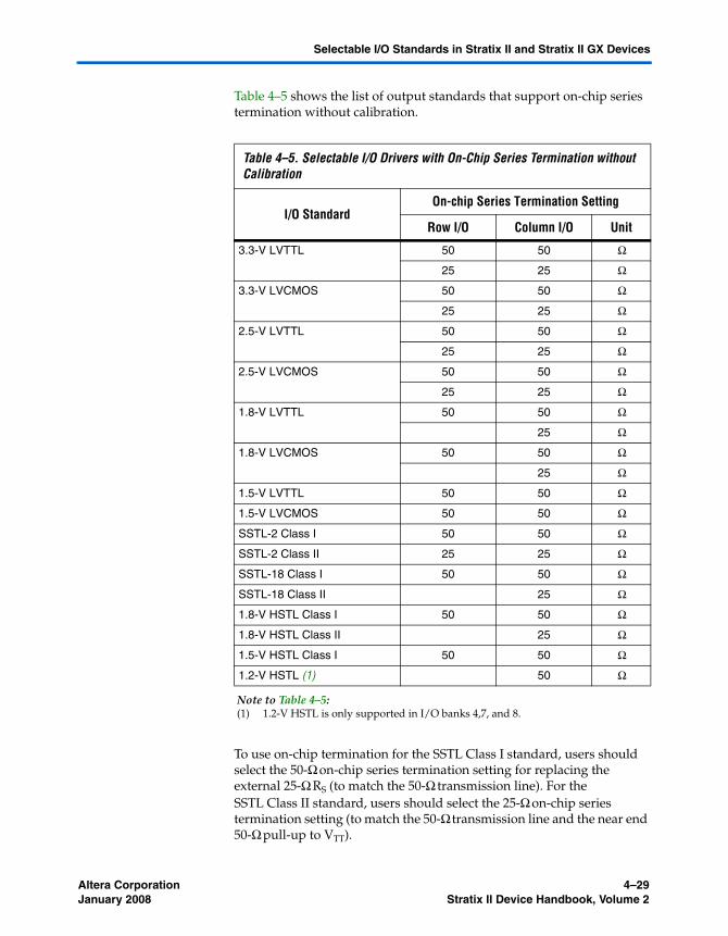
Table 4–5 shows the list of output standards that support on-chip series termination without calibration.
To use on-chip termination for the SSTL Class I standard, users should select the 50-Ω on-chip series termination setting for replacing the external 25-Ω RS (to match the 50-Ω transmission line). For the SSTL Class II standard, users should select the 25-Ω on-chip series termination setting (to match the 50-Ω transmission line and the near end 50-Ω pull-up to VTT).
Table 4–5. Selectable I/O Drivers with On-Chip Series Termination without Calibration
I/O StandardOn-chip Series Termination Setting
Row I/O Column I/O Unit
3.3-V LVTTL 50 50 Ω
25 25 Ω
3.3-V LVCMOS 50 50 Ω
25 25 Ω
2.5-V LVTTL 50 50 Ω
25 25 Ω
2.5-V LVCMOS 50 50 Ω
25 25 Ω
1.8-V LVTTL 50 50 Ω
25 Ω
1.8-V LVCMOS 50 50 Ω
25 Ω
1.5-V LVTTL 50 50 Ω
1.5-V LVCMOS 50 50 Ω
SSTL-2 Class I 50 50 Ω
SSTL-2 Class II 25 25 Ω
SSTL-18 Class I 50 50 Ω
SSTL-18 Class II 25 Ω
1.8-V HSTL Class I 50 50 Ω
1.8-V HSTL Class II 25 Ω
1.5-V HSTL Class I 50 50 Ω
1.2-V HSTL (1) 50 Ω
Note to Table 4–5:(1) 1.2-V HSTL is only supported in I/O banks 4,7, and 8.
Altera Corporation 4–29January 2008 Stratix II Device Handbook, Volume 2
On-Chip Termination
f For more information on tolerance specifications for on-chip termination without calibration, refer to the DC & Switching Characteristics chapter in volume 1 of the Stratix II Device Handbook or the DC & Switching Characteristics chapter in volume 1 of the Stratix II GX Device Handbook.
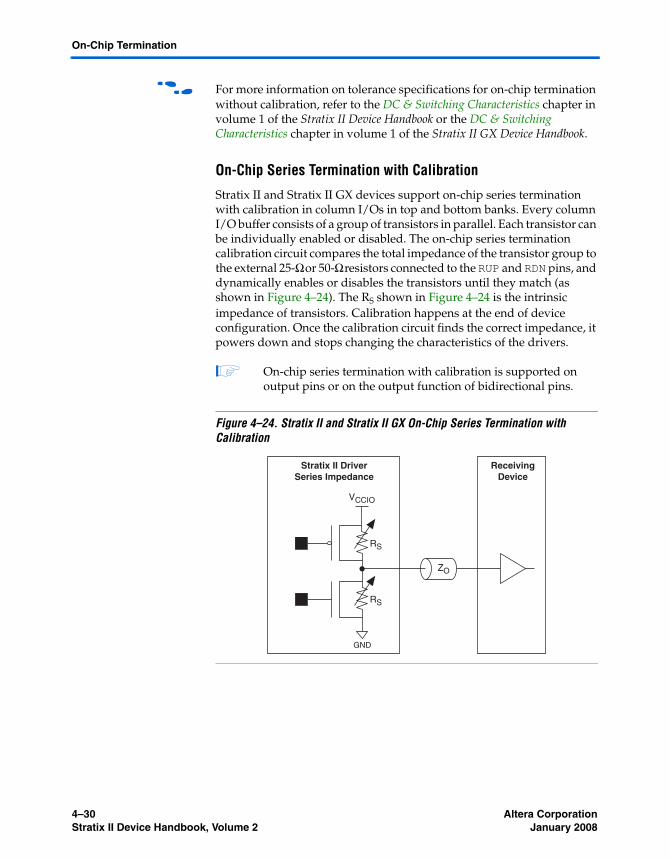
On-Chip Series Termination with Calibration
Stratix II and Stratix II GX devices support on-chip series termination with calibration in column I/Os in top and bottom banks. Every column I/O buffer consists of a group of transistors in parallel. Each transistor can be individually enabled or disabled. The on-chip series termination calibration circuit compares the total impedance of the transistor group to the external 25-Ω or 50-Ω resistors connected to the RUP and RDN pins, and dynamically enables or disables the transistors until they match (as shown in Figure 4–24). The RS shown in Figure 4–24 is the intrinsic impedance of transistors. Calibration happens at the end of device configuration. Once the calibration circuit finds the correct impedance, it powers down and stops changing the characteristics of the drivers.
1 On-chip series termination with calibration is supported on output pins or on the output function of bidirectional pins.
Figure 4–24. Stratix II and Stratix II GX On-Chip Series Termination with Calibration
Stratix II DriverSeries Impedance
ReceivingDevice
VCCIO
RS
RS
ZO
GND
4–30 Altera CorporationStratix II Device Handbook, Volume 2 January 2008

Selectable I/O Standards in Stratix II and Stratix II GX Devices
Table 4–6 shows the list of output standards that support on-chip series termination with calibration.
On-Chip Parallel Termination with Calibration
Stratix II and Stratix II GX devices support on-chip parallel termination with calibration in column I/Os in top and bottom banks. Every column I/O buffer consists of a group of transistors in parallel. Each transistor can be individually enabled or disabled. The on-chip parallel termination calibration circuit compares the total impedance of the transistor group to
Table 4–6. Selectable I/O Drivers with On-Chip Series Termination with Calibration
I/O Standard On-Chip Series Termination Setting (Column I/O) Unit
3.3-V LVTTL 50 Ω
25 Ω
3.3-V LVCMOS 50 Ω
25 Ω
2.5-V LVTTL 50 Ω
25 Ω
2.5-V LVCMOS 50 Ω
25 Ω
1.8-V LVTTL 50 Ω
25 Ω
1.8-V LVCMOS 50 Ω
25 Ω
1.5 LVTTL 50 Ω
1.5 LVCMOS 50 Ω
SSTL-2 Class I 50 Ω
SSTL-2 Class II 25 Ω
SSTL-18 Class I 50 Ω
SSTL-18 Class II 25 Ω
1.8-V HSTL Class I 50 Ω
1.8-V HSTL Class II 25 Ω
1.5-V HSTL Class I 50 Ω
1.2-V HSTL (1) 50 Ω
Note to Table 4–6:(1) 1.2-V HSTL is only supported in I/O banks 4,7, and 8.
Altera Corporation 4–31January 2008 Stratix II Device Handbook, Volume 2

On-Chip Termination
the external 50-Ω resistors connected to the RUP and RDN pins and dynamically enables or disables the transistors until they match. Calibration happens at the end of the device configuration. Once the calibration circuit finds the correct impedance, it powers down and stops changing the characteristics of the drivers.
There are two separate sets of calibration circuits in the Stratix II and Stratix II GX devices:
■ One calibration circuit for top banks 3 and 4■ One calibration circuit for bottom banks 7 and 8
Calibration circuits rely on the external pull-up reference resistor (RUP) and pull-down reference resistor (RDN) to achieve accurate on-chip series and parallel termination. There is one pair of RUP and RDN pins in bank 4 for the calibration circuit for top I/O banks 3 and 4. Similarly, there is one pair of RUP and RDN pins in bank 7 for the calibration circuit for bottom I/O banks 7 and 8. Two banks share the same calibration circuitry, so they must have the same VCCIO voltage if both banks enable on-chip series or parallel termination with calibration. If banks 3 and 4 have different VCCIO voltages, only bank 4 can enable on-chip series or parallel termination with calibration because the RUP and RDN pins are located in bank 4. Bank 3 still can use on-chip series termination, but without calibration. The same rule applies to banks 7 and 8.
Table 4–7. Selectable I/O Drivers with On-Chip Parallel Termination with Calibration
I/O Standard On-Chip Parallel Termination Setting (Column I/O) Unit
SSTL-2 Class I 50 Ω
SSTL-2 Class II 50 Ω
SSTL-18 Class I 50 Ω
SSTL-18 Class II 50 Ω
1.8-V HSTL Class I 50 Ω
1.8-V HSTL Class II 50 Ω
1.5-V HSTL Class I 50 Ω
1.5-V HSTL Class II 50 Ω
1.2-V HSTL (1) 50 Ω
Note to Table 4–7:(1) 1.2-V HSTL is only supported in I/O banks 4,7, and 8.
4–32 Altera CorporationStratix II Device Handbook, Volume 2 January 2008

Selectable I/O Standards in Stratix II and Stratix II GX Devices
1 On-chip parallel termination with calibration is only supported for input pins. Pins configured as bidirectional do not support on-chip parallel termination.
The RUP and RDN pins are dual-purpose I/Os, which means they can be used as regular I/Os if the calibration circuit is not used. When used for calibration, the RUP pin is connected to VCCIO through an external 25-Ω or 50-Ω resistor for an on-chip series termination value of 25 Ω or 50 Ω, respectively. The RDN pin is connected to GND through an external 25-Ω or 50-Ω resistor for an on-chip series termination value of 25 Ω or 50 Ω, respectively. For on-chip parallel termination, the RUP pin is connected to VCCIO through an external 50-Ω resistor, and RDN is connected to GND through an external 50-Ω resistor.
f For more information on tolerance specifications for on-chip termination with calibration, refer to the DC & Switching Characteristics chapter in volume 1 of the Stratix II Device Handbook or the DC & Switching Characteristics chapter in volume 1 of the Stratix II GX Device Handbook.
Design Considerations
While Stratix II and Stratix II GX devices feature various I/O capabilities for high-performance and high-speed system designs, there are several other considerations that require attention to ensure the success of those designs.
I/O Termination
I/O termination requirements for single-ended and differential I/O standards are discussed in this section.
Single-Ended I/O Standards
Although single-ended, non-voltage-referenced I/O standards do not require termination, impedance matching is necessary to reduce reflections and improve signal integrity.
Voltage-referenced I/O standards require both an input reference voltage, VREF, and a termination voltage, VTT. The reference voltage of the receiving device tracks the termination voltage of the transmitting device. Each voltage-referenced I/O standard requires a unique termination setup. For example, a proper resistive signal termination scheme is critical in SSTL standards to produce a reliable DDR memory system with superior noise margin.
Altera Corporation 4–33January 2008 Stratix II Device Handbook, Volume 2
Design Considerations
Stratix II and Stratix II GX on-chip series and parallel termination provides the convenience of no external components. External pull-up resistors can be used to terminate the voltage-referenced I/O standards such as SSTL-2 and HSTL.
1 Refer to the “Stratix II and Stratix II GX I/O Standards Support” on page 4–2 for more information on the termination scheme of various single-ended I/O standards.
Differential I/O Standards
Differential I/O standards typically require a termination resistor between the two signals at the receiver. The termination resistor must match the differential load impedance of the bus. Stratix II and Stratix II GX devices provide an optional differential on-chip resistor when using LVDS and HyperTransport standards.
I/O Banks Restrictions
Each I/O bank can simultaneously support multiple I/O standards. The following sections provide guidelines for mixing non-voltage-referenced and voltage-referenced I/O standards in Stratix II and Stratix II GX devices.
Non-Voltage-Referenced Standards
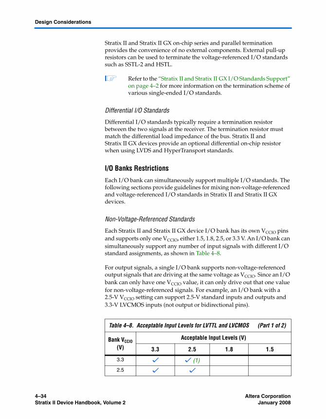
Each Stratix II and Stratix II GX device I/O bank has its own VCCIO pins and supports only one VCCIO, either 1.5, 1.8, 2.5, or 3.3 V. An I/O bank can simultaneously support any number of input signals with different I/O standard assignments, as shown in Table 4–8.
For output signals, a single I/O bank supports non-voltage-referenced output signals that are driving at the same voltage as VCCIO. Since an I/O bank can only have one VCCIO value, it can only drive out that one value for non-voltage-referenced signals. For example, an I/O bank with a 2.5-V VCCIO setting can support 2.5-V standard inputs and outputs and 3.3-V LVCMOS inputs (not output or bidirectional pins).
Table 4–8. Acceptable Input Levels for LVTTL and LVCMOS (Part 1 of 2)
Bank VCCIO (V)
Acceptable Input Levels (V)
3.3 2.5 1.8 1.5
3.3 v v (1)
2.5 v v
4–34 Altera CorporationStratix II Device Handbook, Volume 2 January 2008

Selectable I/O Standards in Stratix II and Stratix II GX Devices
Voltage-Referenced Standards
To accommodate voltage-referenced I/O standards, each Stratix II or Stratix II GX device’s I/O bank supports multiple VREF pins feeding a common VREF bus. The number of available VREF pins increases as device density increases. If these pins are not used as VREF pins, they cannot be used as generic I/O pins. However, each bank can only have a single VCCIO voltage level and a single VREF voltage level at a given time.
An I/O bank featuring single-ended or differential standards can support voltage-referenced standards as long as all voltage-referenced standards use the same VREF setting.
Because of performance reasons, voltage-referenced input standards use their own VCCIO level as the power source. For example, you can only place 1.5-V HSTL input pins in an I/O bank with a 1.5-V VCCIO.
1 Refer to the “Stratix II and Stratix II GX I/O Banks” on page 4–20 for details on input VCCIO for voltage-referenced standards.
Voltage-referenced bidirectional and output signals must be the same as the I/O bank’s VCCIO voltage. For example, you can only place SSTL-2 output pins in an I/O bank with a 2.5-V VCCIO.
1 Refer to the “I/O Placement Guidelines” on page 4–36 for details on voltage-referenced I/O standards placement.
1.8 v (2) v (2) v v (1)
1.5 v (2) v (2) v v
Notes to Table 4–8:(1) Because the input signal does not drive to the rail, the input buffer does not
completely shut off, and the I/O current is slightly higher than the default value.(2) These input values overdrive the input buffer, so the pin leakage current is
slightly higher than the default value. To drive inputs higher than VCCIO but less than 4.0 V, disable the PCI clamping diode and select the Allow LVTTL and LVCMOS input levels to overdrive input buffer option in the Quartus II software.
Table 4–8. Acceptable Input Levels for LVTTL and LVCMOS (Part 2 of 2)
Bank VCCIO (V)
Acceptable Input Levels (V)
3.3 2.5 1.8 1.5
Altera Corporation 4–35January 2008 Stratix II Device Handbook, Volume 2

Design Considerations
Mixing Voltage-Referenced and Non-Voltage-Referenced Standards
An I/O bank can support both non-voltage-referenced and voltage-referenced pins by applying each of the rule sets individually. For example, an I/O bank can support SSTL-18 inputs and 1.8-V inputs and outputs with a 1.8-V VCCIO and a 0.9-V VREF. Similarly, an I/O bank can support 1.5-V standards, 2.5-V (inputs, but not outputs), and HSTL I/O standards with a 1.5-V VCCIO and 0.75-V VREF.
I/O Placement Guidelines
The I/O placement guidelines help to reduce noise issues that may be associated with a design such that Stratix II and Stratix II GX FPGAs can maintain an acceptable noise level on the VCCIO supply. Because Stratix II and Stratix II GX devices require each bank to be powered separately for VCCIO, these noise issues have no effect when crossing bank boundaries and, as such, these rules need not be applied.
This section provides I/O placement guidelines for the programmable I/O standards supported by Stratix II and Stratix II GX devices and includes essential information for designing systems using their devices’ selectable I/O capabilities.
VREF Pin Placement Restrictions
There are at least two dedicated VREF pins per I/O bank to drive the VREF bus. Larger Stratix II and Stratix II GX devices have more VREF pins per I/O bank. All VREF pins within one I/O bank are shorted together at device die level.
There are limits to the number of pins that a VREF pin can support. For example, each output pin adds some noise to the VREF level and an excessive number of outputs make the level too unstable to be used for incoming signals.
Restrictions on the placement of single-ended voltage-referenced I/O pads with respect to VREF pins help maintain an acceptable noise level on the VCCIO supply and prevent output switching noise from shifting the VREF rail.
Input PinsEach VREF pin supports a maximum of 40 input pads.
4–36 Altera CorporationStratix II Device Handbook, Volume 2 January 2008
Selectable I/O Standards in Stratix II and Stratix II GX Devices
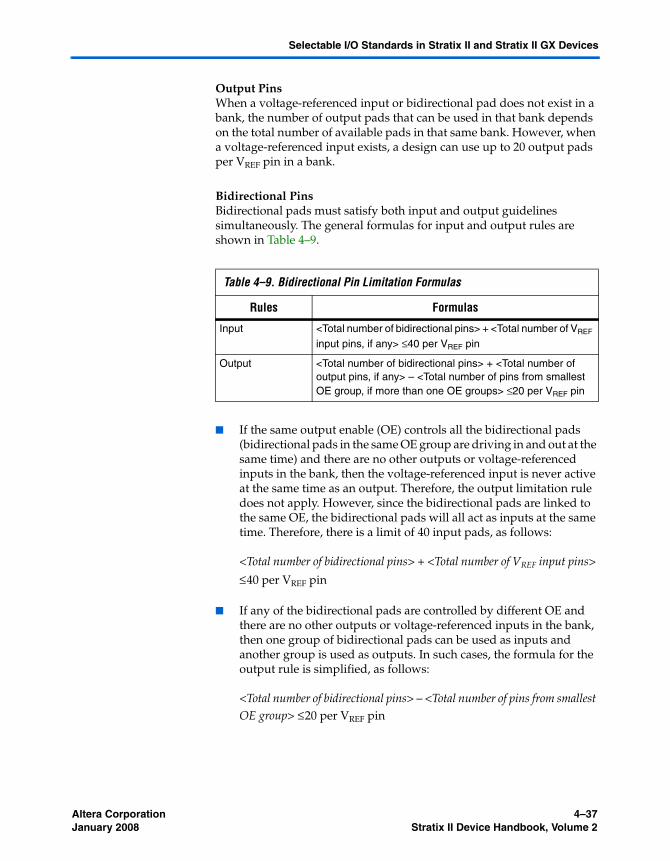
Output PinsWhen a voltage-referenced input or bidirectional pad does not exist in a bank, the number of output pads that can be used in that bank depends on the total number of available pads in that same bank. However, when a voltage-referenced input exists, a design can use up to 20 output pads per VREF pin in a bank.
Bidirectional PinsBidirectional pads must satisfy both input and output guidelines simultaneously. The general formulas for input and output rules are shown in Table 4–9.
■ If the same output enable (OE) controls all the bidirectional pads (bidirectional pads in the same OE group are driving in and out at the same time) and there are no other outputs or voltage-referenced inputs in the bank, then the voltage-referenced input is never active at the same time as an output. Therefore, the output limitation rule does not apply. However, since the bidirectional pads are linked to the same OE, the bidirectional pads will all act as inputs at the same time. Therefore, there is a limit of 40 input pads, as follows:
<Total number of bidirectional pins> + <Total number of VREF input pins>
≤ 40 per VREF pin
■ If any of the bidirectional pads are controlled by different OE and there are no other outputs or voltage-referenced inputs in the bank, then one group of bidirectional pads can be used as inputs and another group is used as outputs. In such cases, the formula for the output rule is simplified, as follows:
<Total number of bidirectional pins> – <Total number of pins from smallest OE group> ≤ 20 per VREF pin
Table 4–9. Bidirectional Pin Limitation Formulas
Rules Formulas
Input <Total number of bidirectional pins> + <Total number of VREF input pins, if any> ≤ 40 per VREF pin
Output <Total number of bidirectional pins> + <Total number of output pins, if any> – <Total number of pins from smallest OE group, if more than one OE groups> ≤ 20 per VREF pin
Altera Corporation 4–37January 2008 Stratix II Device Handbook, Volume 2
Design Considerations
■ Consider a case where eight bidirectional pads are controlled by OE1, eight bidirectional pads are controlled by OE2, six bidirectional pads are controlled by OE3, and there are no other outputs or voltage-referenced inputs in the bank. While this totals 22 bidirectional pads, it is safely allowable because there would be a possible maximum of 16 outputs per VREF pin, assuming the worst case where OE1 and OE2 are active and OE3 is inactive. This is useful for DDR SDRAM applications.
■ When at least one additional voltage-referenced input and no other outputs exist in the same VREF group, the bidirectional pad limitation must simultaneously adhere to the input and output limitations. The input rule becomes:
<Total number of bidirectional pins> + <Total number of VREF input pins>
≤ 40 per VREF pin
Whereas the output rule is simplified as:
<Total number of bidirectional pins> ≤ 20 per VREF pin
■ When at least one additional output exists but no voltage-referenced inputs exist, the output rule becomes:
<Total number of bidirectional pins> + <Total number of output pins> – <Total number of pins from smallest OE group> ≤ 20 per VREF pin
■ When additional voltage-referenced inputs and other outputs exist in the same VREF group, then the bidirectional pad limitation must again simultaneously adhere to the input and output limitations. The input rule is:
<Total number of bidirectional pins> + <Total number of VREF input pins>
≤ 40 per VREF pin
Whereas the output rule is given as:
<Total number of bidirectional pins> + <Total number of output pins> – <Total number of pins from smallest OE group> ≤ 20 per VREF pin
I/O Pin Placement with Respect to High-Speed Differential I/O Pins
Regardless of whether or not the SERDES circuitry is utilized, there is a restriction on the placement of single-ended output pins with respect to high-speed differential I/O pins. As shown in Figure 4–25, all
4–38 Altera CorporationStratix II Device Handbook, Volume 2 January 2008

Selectable I/O Standards in Stratix II and Stratix II GX Devices
single-ended outputs must be placed at least one LAB row away from the differential I/O pins. There are no restrictions on the placement of single-ended input pins with respect to differential I/O pins. Single-ended input pins may be placed within the same LAB row as differential I/O pins. However, the single-ended input’s IOE register is not available. The input must be implemented within the core logic.
This single-ended output pin placement restriction only applies when using the LVDS or HyperTransport I/O standards in the left and right I/O banks. There are no restrictions for single-ended output pin placement with respect to differential clock pins in the top and bottom I/O banks.
Figure 4–25. Single-Ended Output Pin Placement with Respect to Differential I/O Pins
DC Guidelines
Power budgets are essential to ensure the reliability and functionality of a system application. You are often required to perform power dissipation analysis on each device in the system to come out with the total power dissipated in that system, which is composed of a static component and a dynamic component.
The static power consumption of a device is the total DC current flowing from VCCIO to ground.
Single-Ended Output Pin
Differential I/O Pin
Single_Ended Input
Single-Ended OutputsNot Allowed
Row Boundary
Altera Corporation 4–39January 2008 Stratix II Device Handbook, Volume 2
Design Considerations
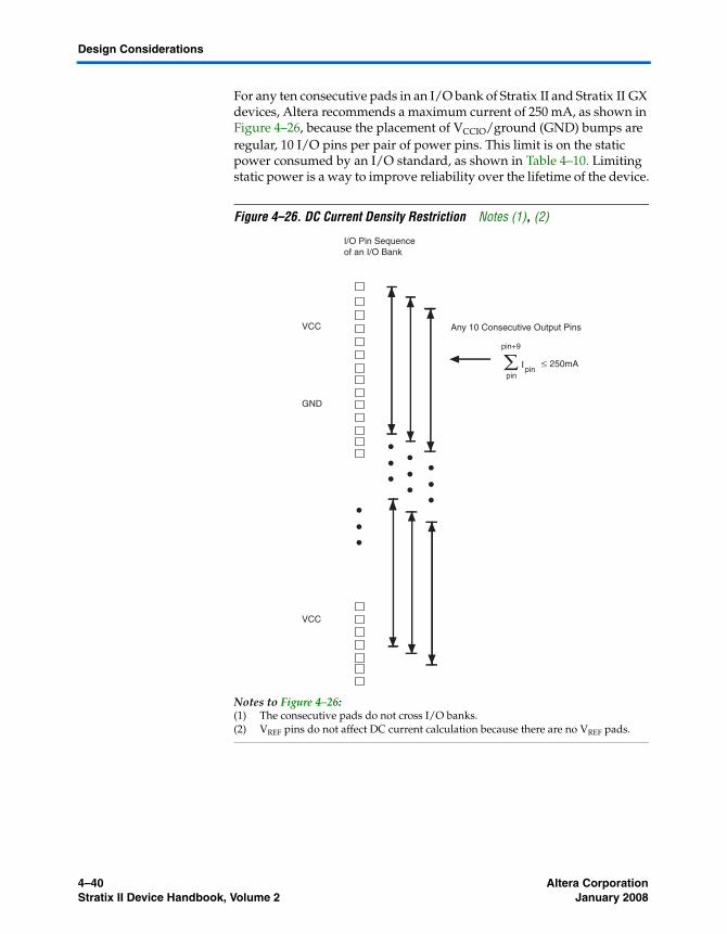
For any ten consecutive pads in an I/O bank of Stratix II and Stratix II GX devices, Altera recommends a maximum current of 250 mA, as shown in Figure 4–26, because the placement of VCCIO/ground (GND) bumps are regular, 10 I/O pins per pair of power pins. This limit is on the static power consumed by an I/O standard, as shown in Table 4–10. Limiting static power is a way to improve reliability over the lifetime of the device.
Figure 4–26. DC Current Density Restriction Notes (1), (2)
Notes to Figure 4–26:(1) The consecutive pads do not cross I/O banks.(2) VREF pins do not affect DC current calculation because there are no VREF pads.
I/O Pin Sequenceof an I/O Bank
Any 10 Consecutive Output Pins
pin+9
pinpin
≤ 250mAI
VCC
GND
VCC
∑
4–40 Altera CorporationStratix II Device Handbook, Volume 2 January 2008

Selectable I/O Standards in Stratix II and Stratix II GX Devices
Table 4–10 shows the I/O standard DC current specification.
Table 4–10. Stratix II and Stratix II GX I/O Standard DC Current Specification (Part 1 of 2) Note (1)
I/O Standard IPIN (mA), Top and Bottom I/O Banks IPIN (mA), Left and Right I/O Banks(2)
LVTTL (3) (3)
LVCMOS (3) (3)
2.5 V (3) (3)
1.8 V (3) (3)
1.5 V (3) (3)
3.3-V PCI 1.5 NA
3.3-V PCI-X 1.5 NA
SSTL-2 Class I 12 (4) 12 (4)
SSTL-2 Class II 24 (4) 16 (4)
SSTL-18 Class I 12 (4) 10 (4)
SSTL-18 Class II 20 (4) NA
1.8-V HSTL Class I 12 (4) 12
1.8-V HSTL Class II 20 (4) NA
1.5-V HSTL Class I 12 (4) 8
1.5-V HSTL Class II 20 (4) NA
Differential SSTL-2 Class I 12 12
Differential SSTL-2 Class II 24 16
Differential SSTL-18 Class I 12 10
Differential SSTL-18 Class II 20 NA
1.8-V differential HSTL Class I 12 12
1.8-V differential HSTL Class II 20 NA
1.5-V differential HSTL Class I 12 8
1.5-V differential HSTL Class II 20 NA
Altera Corporation 4–41January 2008 Stratix II Device Handbook, Volume 2

Conclusion
Table 4–10 only shows the limit on the static power consumed by an I/O standard. The amount of power used at any moment could be much higher, and is based on the switching activities.
Conclusion Stratix II and Stratix II GX devices provide I/O capabilities that allow you to work in compliance with current and emerging I/O standards and requirements. With the Stratix II or Stratix II GX devices features, such as programmable driver strength, you can reduce board design interface costs and increase the development flexibility.
References Refer to the following references for more information:
■ Interface Standard for Nominal 3V/ 3.3-V Supply Digital Integrated Circuits, JESD8-B, Electronic Industries Association, September 1999.
■ 2.5-V +/- 0.2V (Normal Range) and 1.8-V to 2.7V (Wide Range) Power Supply Voltage and Interface Standard for Non-terminated Digital Integrated Circuits, JESD8-5, Electronic Industries Association, October 1995.
■ 1.8-V +/- 0.15 V (Normal Range) and 1.2 V - 1.95 V (Wide Range) Power Supply Voltage and Interface Standard for Non-terminated Digital Integrated Circuits, JESD8-7, Electronic Industries Association, February 1997.
■ 1.5-V +/- 0.1 V (Normal Range) and 0.9 V - 1.6 V (Wide Range) Power Supply Voltage and Interface Standard for Non-terminated Digital Integrated Circuits, JESD8-11, Electronic Industries Association, October 2000.
Notes to Table 4–10:(1) The current value obtained for differential HSTL and differential SSTL standards is per pin and not per differential
pair, as opposed to the per-pair current value of LVDS and HyperTransport standards.(2) This does not apply to the right I/O banks of Stratix II GX devices. Stratix II GX devices have transceivers on the
right I/O banks.(3) The DC power specification of each I/O standard depends on the current sourcing and sinking capabilities of the
I/O buffer programmed with that standard, as well as the load being driven. LVTTL, LVCMOS, 2.5-V, 1.8-V, and 1.5-V outputs are not included in the static power calculations because they normally do not have resistor loads in real applications. The voltage swing is rail-to-rail with capacitive load only. There is no DC current in the system.
(4) This IPIN value represents the DC current specification for the default current strength of the I/O standard. The IPIN varies with programmable drive strength and is the same as the drive strength as set in Quartus II software. Refer to the Stratix II Architecture chapter in volume 1 of the Stratix II Device Handbook or the Stratix II GX Architecture chapter in volume 1 of the Stratix II GX Device Handbook for a detailed description of the programmable drive strength feature of voltage-referenced I/O standards.
Table 4–10. Stratix II and Stratix II GX I/O Standard DC Current Specification (Part 2 of 2) Note (1)
I/O Standard IPIN (mA), Top and Bottom I/O Banks IPIN (mA), Left and Right I/O Banks(2)
4–42 Altera CorporationStratix II Device Handbook, Volume 2 January 2008
Selectable I/O Standards in Stratix II and Stratix II GX Devices
■ PCI Local Bus Specification, Revision 2.2, PCI Special Interest Group, December 1998.
■ PCI-X Local Bus Specification, Revision 1.0a, PCI Special Interest Group.
■ Stub Series Terminated Logic for 2.5-V (SSTL-2), JESD8-9A, Electronic Industries Association, December 2000.
■ Stub Series Terminated Logic for 1.8 V (SSTL-18), Preliminary JC42.3, Electronic Industries Association.
■ High-Speed Transceiver Logic (HSTL)—A 1.5-V Output Buffer Supply Voltage Based Interface Standard for Digital Integrated Circuits, EIA/JESD8-6, Electronic Industries Association, August 1995.
■ Electrical Characteristics of Low Voltage Differential Signaling (LVDS) Interface Circuits, ANSI/TIA/EIA-644, American National Standards Institute/Telecommunications Industry/Electronic Industries Association, October 1995.
Referenced Documents
This chapter references the following documents:
■ DC & Switching Characteristics chapter in volume 1 of the Stratix II Device Handbook
■ DC & Switching Characteristics chapter in volume 1 of the Stratix II GX Device Handbook
■ External Memory Interfaces in Stratix II & Stratix II GX Devices chapter in volume 2 of the Stratix II Device Handbook
■ External Memory Interfaces in Stratix II & Stratix II GX Devices chapter in volume 2 of the Stratix II GX Device Handbook
■ High-Speed Differential I/O Interfaces with DPA in Stratix II & Stratix II GX Devices chapter in volume 2 of the Stratix II Device Handbook
■ High-Speed Differential I/O Interfaces with DPA in Stratix II & Stratix II GX Devices chapter in volume 2 of the Stratix II GX Device Handbook
■ PLLs in Stratix II & Stratix II GX Devices chapter in volume 2 of the Stratix II Device Handbook
■ PLLs in Stratix II & Straix II GX Devices chapter in volume 2 of the Stratix II GX Device Handbook
■ Stratix II Architecture chapter in volume 1 of the Stratix II Device Handbook
■ Stratix II GX Architecture chapter in volume 1 of the Stratix II GX Device Handbook
■ Stratix II GX Transceiver User Guide (volume 1) of the Stratix II GX Device Handbook
Altera Corporation 4–43January 2008 Stratix II Device Handbook, Volume 2

Document Revision History
Document Revision History
Table 4–11 shows the revision history for this chapter.
Table 4–11. Document Revision History (Part 1 of 2)
Date and Document
VersionChanges Made Summary of Changes
January 2008 v4.6
Updated Figure 4–22. —
Updated Note 4 to Table 4–2. —
Added “Referenced Documents” section. —
Minor text edits. —
No change For the Stratix II GX Device Handbook only:Formerly chapter 9. The chapter number changed due to the addition of the Stratix II GX Dynamic Reconfiguration chapter. No content change.
—
May 2007v4.5
Added a note to the “On-Chip Series Termination with Calibration” section.
—
Added a note to the “On-Chip Series Termination without Calibration” section
—
Updated note to the “Stratix II and Stratix II GX I/O Features” section.
—
Updated the “LVDS” section. —
Updated note to “1.5 V” section —
● Updated Note (1) for Table 10–4● Updated Note (2) for Table 10–3
—
Updated Table 10–2, column heading for columns 9 and 10.
—
Updated Table 10–10. —
Fixed typo in the “Stratix II and Stratix II GX I/O Features” section
—
February 2007v4.4
Added the “Document Revision History” section to this chapter.
—
August 2006 v4.3
Updated Table 9–2, Table 9–4, Table 9–5, Table 9–6, and Table 9–7.
—
April 2006 v4.2 Chapter updated as part of the Stratix II Device Handbook update.
—
No change Formerly chapter 8. Chapter number change only due to chapter addition to Section I in February 2006; no content change.
—
4–44 Altera CorporationStratix II Device Handbook, Volume 2 January 2008
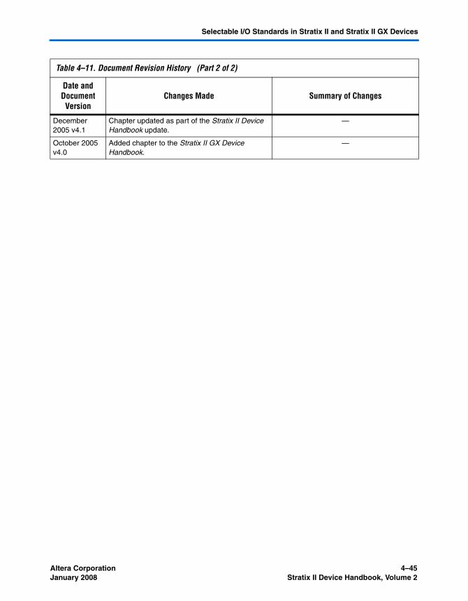
Selectable I/O Standards in Stratix II and Stratix II GX Devices
December 2005 v4.1
Chapter updated as part of the Stratix II Device Handbook update.
—
October 2005v4.0
Added chapter to the Stratix II GX Device Handbook.
—
Table 4–11. Document Revision History (Part 2 of 2)
Date and Document
VersionChanges Made Summary of Changes
Altera Corporation 4–45January 2008 Stratix II Device Handbook, Volume 2
Document Revision History
4–46 Altera CorporationStratix II Device Handbook, Volume 2 January 2008