operating stratix conditions - altera
TRANSCRIPT

Altera Corporation 5–1April 2011
5. DC & SwitchingCharacteristics
Operating Conditions
Stratix® II devices are offered in both commercial and industrial grades. Industrial devices are offered in -4 speed grades and commercial devices are offered in -3 (fastest), -4, -5 speed grades.
Tables 5–1 through 5–32 provide information about absolute maximum ratings, recommended operating conditions, DC electrical characteristics, and other specifications for Stratix II devices.
Absolute Maximum Ratings
Table 5–1 contains the absolute maximum ratings for the Stratix II device family.
Table 5–1. Stratix II Device Absolute Maximum Ratings Notes (1), (2), (3)
Symbol Parameter Conditions Minimum Maximum Unit
VCCINT Supply voltage With respect to ground –0.5 1.8 V
VCCIO Supply voltage With respect to ground –0.5 4.6 V
VCCPD Supply voltage With respect to ground –0.5 4.6 V
VCCA Analog power supply for PLLs
With respect to ground –0.5 1.8 V
VCCD Digital power supply for PLLs With respect to ground –0.5 1.8 V
VI DC input voltage (4) –0.5 4.6 V
IOUT DC output current, per pin –25 40 mA
TSTG Storage temperature No bias –65 150 °C
TJ Junction temperature BGA packages under bias –55 125 °C
Notes to Tables 5–1(1) See the Operating Requirements for Altera Devices Data Sheet.(2) Conditions beyond those listed in Table 5–1 may cause permanent damage to a device. Additionally, device
operation at the absolute maximum ratings for extended periods of time may have adverse affects on the device.(3) Supply voltage specifications apply to voltage readings taken at the device pins, not at the power supply.(4) During transitions, the inputs may overshoot to the voltage shown in Table 5–2 based upon the input duty cycle.
The DC case is equivalent to 100% duty cycle. During transitions, the inputs may undershoot to –2.0 V for input currents less than 100 mA and periods shorter than 20 ns.
SII51005-4.5

5–2 Altera CorporationStratix II Device Handbook, Volume 1 April 2011
Operating Conditions
Recommended Operating Conditions
Table 5–3 contains the Stratix II device family recommended operating conditions.
Table 5–2. Maximum Duty Cycles in Voltage Transitions
Symbol Parameter Condition Maximum Duty Cycles Unit
VI Maximum duty cycles in voltage transitions
VI = 4.0 V 100 %
VI = 4.1 V 90 %
VI = 4.2 V 50 %
VI = 4.3 V 30 %
VI = 4.4 V 17 %
VI = 4.5 V 10 %
Table 5–3. Stratix II Device Recommended Operating Conditions (Part 1 of 2) Note (1)
Symbol Parameter Conditions Minimum Maximum Unit
VCCINT Supply voltage for internal logic 100 μs ≤ risetime ≤ 100 ms (3) 1.15 1.25 V
VCCIO Supply voltage for input and output buffers, 3.3-V operation
100 μs ≤ risetime ≤ 100 ms (3), (6) 3.135 (3.00)
3.465 (3.60)
V
Supply voltage for input and output buffers, 2.5-V operation
100 μs ≤ risetime ≤ 100 ms (3) 2.375 2.625 V
Supply voltage for input and output buffers, 1.8-V operation
100 μs ≤ risetime ≤ 100 ms (3) 1.71 1.89 V
Supply voltage for output buffers, 1.5-V operation
100 μs ≤ risetime ≤ 100 ms (3) 1.425 1.575 V
Supply voltage for input and output buffers, 1.2-V operation
100 μs ≤ risetime ≤ 100 ms (3) 1.14 1.26 V
VCCPD Supply voltage for pre-drivers as well as configuration and JTAG I/O buffers.
100 μs ≤ risetime ≤ 100 ms (4) 3.135 3.465 V
VCCA Analog power supply for PLLs 100 μs ≤ risetime ≤ 100 ms (3) 1.15 1.25 V
VCCD Digital power supply for PLLs 100 μs ≤ risetime ≤ 100 ms (3) 1.15 1.25 V
VI Input voltage (see Table 5–2) (2), (5) –0.5 4.0 V
VO Output voltage 0 VCCIO V

Altera Corporation 5–3April 2011 Stratix II Device Handbook, Volume 1
DC & Switching Characteristics
DC Electrical Characteristics
Table 5–4 shows the Stratix II device family DC electrical characteristics.
TJ Operating junction temperature For commercial use 0 85 °C
For industrial use –40 100 °C
For military use (7) –55 125 °C
Notes to Table 5–3:(1) Supply voltage specifications apply to voltage readings taken at the device pins, not at the power supply.(2) During transitions, the inputs may overshoot to the voltage shown in Table 5–2 based upon the input duty cycle.
The DC case is equivalent to 100% duty cycle. During transitions, the inputs may undershoot to –2.0 V for input currents less than 100 mA and periods shorter than 20 ns.
(3) Maximum VCC rise time is 100 ms, and VCC must rise monotonically from ground to VC C .(4) VCCPD must ramp-up from 0 V to 3.3 V within 100 μs to 100 ms. If VC C P D is not ramped up within this specified
time, your Stratix II device does not configure successfully. If your system does not allow for a VCCPD ramp-up time of 100 ms or less, you must hold nCONFIG low until all power supplies are reliable.
(5) All pins, including dedicated inputs, clock, I/O, and JTAG pins, may be driven before VCCINT, VCCPD, and VCCIO are powered.
(6) VC C I O maximum and minimum conditions for PCI and PCI-X are shown in parentheses.(7) For more information, refer to the Stratix II Military Temperature Range Support technical brief.
Table 5–3. Stratix II Device Recommended Operating Conditions (Part 2 of 2) Note (1)
Symbol Parameter Conditions Minimum Maximum Unit
Table 5–4. Stratix II Device DC Operating Conditions (Part 1 of 2) Note (1)
Symbol Parameter Conditions Minimum Typical Maximum Unit
II Input pin leakage current VI = VCCIOmax to 0 V (2) –10 10 μA
IOZ Tri-stated I/O pin leakage current
VO = VCCIOmax to 0 V (2) –10 10 μA
IC CI NT 0 VCCINT supply current (standby)
VI = ground, no load, no toggling inputsTJ = 25° C
EP2S15 0.25 (3) A
EP2S30 0.30 (3) A
EP2S60 0.50 (3) A
EP2S90 0.62 (3) A
EP2S130 0.82 (3) A
EP2S180 1.12 (3) A
ICCPD0 VCCPD supply current (standby)
VI = ground, no load, no toggling inputsTJ = 25° C, VCCPD = 3.3V
EP2S15 2.2 (3) mA
EP2S30 2.7 (3) mA
EP2S60 3.6 (3) mA
EP2S90 4.3 (3) mA
EP2S130 5.4 (3) mA
EP2S180 6.8 (3) mA

5–4 Altera CorporationStratix II Device Handbook, Volume 1 April 2011
Operating Conditions
I/O Standard Specifications
Tables 5–5 through 5–32 show the Stratix II device family I/O standard specifications.
ICCI00 VCCIO supply current (standby)
VI = ground, no load, no toggling inputsTJ = 25° C
EP2S15 4.0 (3) mA
EP2S30 4.0 (3) mA
EP2S60 4.0 (3) mA
EP2S90 4.0 (3) mA
EP2S130 4.0 (3) mA
EP2S180 4.0 (3) mA
RCONF (4) Value of I/O pin pull-up resistor before and during configuration
Vi = 0; VCCIO = 3.3 V 10 25 50 kΩ
Vi = 0; VCCIO = 2.5 V 15 35 70 kΩ
Vi = 0; VCCIO = 1.8 V 30 50 100 kΩ
Vi = 0; VCCIO = 1.5 V 40 75 150 kΩ
Vi = 0; VCCIO = 1.2 V 50 90 170 kΩ
Recommended value of I/O pin external pull-down resistor before and during configuration
1 2 kΩ
Notes to Table 5–4:(1) Typical values are for TA = 25°C, VCCINT = 1.2 V, and VCCIO = 1.5 V, 1.8 V, 2.5 V, and 3.3 V.(2) This value is specified for normal device operation. The value may vary during power-up. This applies for all
VCCIO settings (3.3, 2.5, 1.8, and 1.5 V).(3) Maximum values depend on the actual TJ and design utilization. See the Excel-based PowerPlay Early Power
Estimator (available at www.altera.com) or the Quartus II PowerPlay Power Analyzer feature for maximum values. See the section “Power Consumption” on page 5–20 for more information.
(4) Pin pull-up resistance values are lower if an external source drives the pin higher than VCCIO.
Table 5–4. Stratix II Device DC Operating Conditions (Part 2 of 2) Note (1)
Symbol Parameter Conditions Minimum Typical Maximum Unit
Table 5–5. LVTTL Specifications (Part 1 of 2)
Symbol Parameter Conditions Minimum Maximum Unit
VCCIO (1) Output supply voltage 3.135 3.465 V
VI H High-level input voltage 1.7 4.0 V
VIL Low-level input voltage –0.3 0.8 V
VOH High-level output voltage IOH = –4 mA (2) 2.4 V
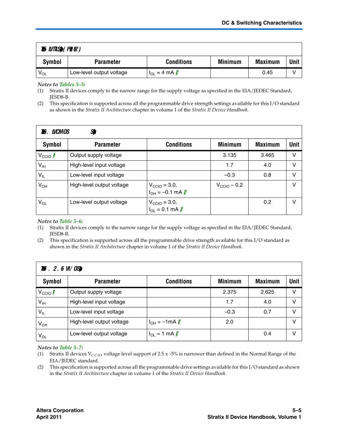
Altera Corporation 5–5April 2011 Stratix II Device Handbook, Volume 1
DC & Switching Characteristics
VOL Low-level output voltage IOL = 4 mA (2) 0.45 V
Notes to Tables 5–5:(1) Stratix II devices comply to the narrow range for the supply voltage as specified in the EIA/JEDEC Standard,
JESD8-B.(2) This specification is supported across all the programmable drive strength settings available for this I/O standard
as shown in the Stratix II Architecture chapter in volume 1 of the Stratix II Device Handbook.
Table 5–6. LVCMOS Specifications
Symbol Parameter Conditions Minimum Maximum Unit
VCCIO (1) Output supply voltage 3.135 3.465 V
VIH High-level input voltage 1.7 4.0 V
VIL Low-level input voltage –0.3 0.8 V
VOH High-level output voltage VCCIO = 3.0, IOH = –0.1 mA (2)
VCCIO – 0.2 V
VOL Low-level output voltage VCCIO = 3.0,IOL = 0.1 mA (2)
0.2 V
Notes to Table 5–6:(1) Stratix II devices comply to the narrow range for the supply voltage as specified in the EIA/JEDEC Standard,
JESD8-B.(2) This specification is supported across all the programmable drive strength available for this I/O standard as
shown in the Stratix II Architecture chapter in volume 1 of the Stratix II Device Handbook.
Table 5–7. 2.5-V I/O Specifications
Symbol Parameter Conditions Minimum Maximum Unit
VCCIO (1) Output supply voltage 2.375 2.625 V
VIH High-level input voltage 1.7 4.0 V
VIL Low-level input voltage –0.3 0.7 V
VOHHigh-level output voltage IOH = –1mA (2) 2.0 V
VOLLow-level output voltage IOL = 1 mA (2) 0.4 V
Notes to Table 5–7:(1) Stratix II devices VC C I O voltage level support of 2.5 ± -5% is narrower than defined in the Normal Range of the
EIA/JEDEC standard.(2) This specification is supported across all the programmable drive settings available for this I/O standard as shown
in the Stratix II Architecture chapter in volume 1 of the Stratix II Device Handbook.
Table 5–5. LVTTL Specifications (Part 2 of 2)
Symbol Parameter Conditions Minimum Maximum Unit

5–6 Altera CorporationStratix II Device Handbook, Volume 1 April 2011
Operating Conditions
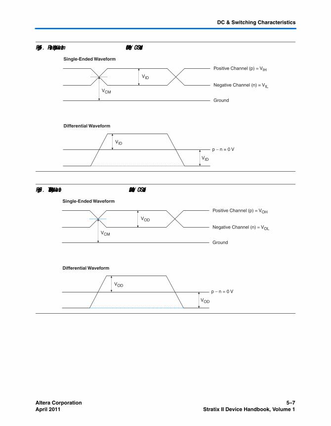
Figures 5–1 and 5–2 show receiver input and transmitter output waveforms, respectively, for all differential I/O standards (LVDS, LVPECL, and HyperTransport technology).
Table 5–8. 1.8-V I/O Specifications
Symbol Parameter Conditions Minimum Maximum Unit
VCCIO (1) Output supply voltage 1.71 1.89 V
VI H High-level input voltage 0.65 × VCCIO 2.25 V
VIL Low-level input voltage –0.30 0.35 × VCCIO V
VOH High-level output voltage IOH = –2 mA (2) VCCIO – 0.45 V
VOL Low-level output voltage IOL = 2 mA (2) 0.45 V
Notes to Table 5–8:(1) The Stratix II device family’s VC C I O voltage level support of 1.8 ± -5% is narrower than defined in the Normal
Range of the EIA/JEDEC standard.(2) This specification is supported across all the programmable drive settings available for this I/O standard as shown
in the Stratix II Architecture chapter in volume 1 of the Stratix II Device Handbook.
Table 5–9. 1.5-V I/O Specifications
Symbol Parameter Conditions Minimum Maximum Unit
VCCIO (1) Output supply voltage 1.425 1.575 V
VI H High-level input voltage 0.65 × VCCIO VCCIO + 0.30 V
VIL Low-level input voltage –0.30 0.35 × VCCIO V
VOH High-level output voltage IOH = –2 mA (2) 0.75 × VCCIO V
VOL Low-level output voltage IOL = 2 mA (2) 0.25 × VCCIO V
Notes to Table 5–9:(1) The Stratix II device family’s VC C I O voltage level support of 1.5 ± -5% is narrower than defined in the Normal
Range of the EIA/JEDEC standard.(2) This specification is supported across all the programmable drive settings available for this I/O standard as shown
in the Stratix II Architecture chapter in volume 1 of the Stratix II Device Handbook.
Altera Corporation 5–7April 2011 Stratix II Device Handbook, Volume 1
DC & Switching Characteristics
Figure 5–1. Receiver Input Waveforms for Differential I/O Standards
Figure 5–2. Transmitter Output Waveforms for Differential I/O Standards
Single-Ended Waveform
Differential Waveform
Positive Channel (p) = VIH
Negative Channel (n) = VIL
Ground
VID
VID
VID
p − n = 0 V
VCM
Single-Ended Waveform
Differential Waveform
Positive Channel (p) = VOH
Negative Channel (n) = VOL
Ground
VOD
VOD
VOD
p − n = 0 V
VCM

5–8 Altera CorporationStratix II Device Handbook, Volume 1 April 2011
Operating Conditions
Table 5–10. 2.5-V LVDS I/O Specifications
Symbol Parameter Conditions Minimum Typical Maximum Unit
VCCIO I/O supply voltage for left and right I/O banks (1, 2, 5, and 6)
2.375 2.500 2.625 V
VID Input differential voltage swing (single-ended)
100 350 900 mV
VICM Input common mode voltage 200 1,250 1,800 mV
VOD Output differential voltage (single-ended)
RL = 100 Ω 250 450 mV
VOCM Output common mode voltage
RL = 100 Ω 1.125 1.375 V
RL Receiver differential input discrete resistor (external to Stratix II devices)
90 100 110 Ω
Table 5–11. 3.3-V LVDS I/O Specifications
Symbol Parameter Conditions Minimum Typical Maximum Unit
VCCIO (1) I/O supply voltage for top and bottom PLL banks (9, 10, 11, and 12)
3.135 3.300 3.465 V
VID Input differential voltage swing (single-ended)
100 350 900 mV
VICM Input common mode voltage 200 1,250 1,800 mV
VOD Output differential voltage (single-ended)
RL = 100 Ω 250 710 mV
VOCM Output common mode voltage
RL = 100 Ω 840 1,570 mV
RL Receiver differential input discrete resistor (external to Stratix II devices)
90 100 110 Ω
Note to Table 5–11:(1) The top and bottom clock input differential buffers in I/O banks 3, 4, 7, and 8 are powered by VCCINT, not VCCIO.
The PLL clock output/feedback differential buffers are powered by VCC_PLL_OUT. For differential clock output/feedback operation, VCC_PLL_OUT should be connected to 3.3 V.

Altera Corporation 5–9April 2011 Stratix II Device Handbook, Volume 1
DC & Switching Characteristics
Table 5–12. LVPECL Specifications
Symbol Parameter Conditions Minimum Typical Maximum Unit
VCCIO (1) I/O supply voltage 3.135 3.300 3.465 V
VID Input differential voltage swing (single-ended)
300 600 1,000 mV
VICM Input common mode voltage 1.0 2.5 V
VOD Output differential voltage (single-ended)
RL = 100 Ω 525 970 mV
VOCM Output common mode voltage
RL = 100 Ω 1,650 2,250 mV
RL Receiver differential input resistor
90 100 110 Ω
Note to Table 5–12:(1) The top and bottom clock input differential buffers in I/O banks 3, 4, 7, and 8 are powered by VCCINT, not VCCIO.
The PLL clock output/feedback differential buffers are powered by VCC_PLL_OUT. For differential clock output/feedback operation, VCC_PLL_OUT should be connected to 3.3 V.
Table 5–13. HyperTransport Technology Specifications
Symbol Parameter Conditions Minimum Typical Maximum Unit
VCCIO I/O supply voltage for left and right I/O banks (1, 2, 5, and 6)
2.375 2.500 2.625 V
VID Input differential voltage swing (single-ended)
RL = 100 Ω 300 600 900 mV
VICM Input common mode voltage RL = 100 Ω 385 600 845 mV
VOD Output differential voltage (single-ended)
RL = 100 Ω 400 600 820 mV
Δ VOD Change in VOD between high and low
RL = 100 Ω 75 mV
VOCM Output common mode voltage RL = 100 Ω 440 600 780 mV
Δ VOCM Change in VOCM between high and low
RL = 100 Ω 50 mV
RL Receiver differential input resistor
90 100 110 Ω
Table 5–14. 3.3-V PCI Specifications (Part 1 of 2)
Symbol Parameter Conditions Minimum Typical Maximum Unit
VCCIO Output supply voltage 3.0 3.3 3.6 V
VIH High-level input voltage 0.5 × VCCIO VCCIO + 0.5 V

5–10 Altera CorporationStratix II Device Handbook, Volume 1 April 2011
Operating Conditions
VIL Low-level input voltage –0.3 0.3 × VCCIO V
VOH High-level output voltage IOUT = –500 μA 0.9 × VCCIO V
VOL Low-level output voltage IOUT = 1,500 μA 0.1 × VCCIO V
Table 5–15. PCI-X Mode 1 Specifications
Symbol Parameter Conditions Minimum Typical Maximum Unit
VCCIO Output supply voltage 3.0 3.6 V
VIH High-level input voltage 0.5 × VCCIO VCCIO + 0.5 V
VIL Low-level input voltage –0.30 0.35 × VCCIO V
VIPU Input pull-up voltage 0.7 × VCCIO V
VOH High-level output voltage IOUT = –500 μA 0.9 × VCCIO V
VOL Low-level output voltage IOUT = 1,500 μA 0.1 × VCCIO V
Table 5–16. SSTL-18 Class I Specifications
Symbol Parameter Conditions Minimum Typical Maximum Unit
VCCIO Output supply voltage 1.71 1.80 1.89 V
VREF Reference voltage 0.855 0.900 0.945 V
VTT Termination voltage VREF – 0.04 VREF VREF + 0.04 V
VIH (DC) High-level DC input voltage VREF + 0.125 V
VIL (DC) Low-level DC input voltage VREF – 0.125 V
VIH (AC) High-level AC input voltage VREF + 0.25 V
VIL (AC) Low-level AC input voltage VREF – 0.25 V
VOH High-level output voltage IOH = –6.7 mA (1) VTT + 0.475 V
VOL Low-level output voltage IOL = 6.7 mA (1) VTT – 0.475 V
Note to Table 5–16:(1) This specification is supported across all the programmable drive settings available for this I/O standard as shown
in the Stratix II Architecture chapter in volume 1 of the Stratix II Device Handbook.
Table 5–14. 3.3-V PCI Specifications (Part 2 of 2)
Symbol Parameter Conditions Minimum Typical Maximum Unit

Altera Corporation 5–11April 2011 Stratix II Device Handbook, Volume 1
DC & Switching Characteristics
Table 5–17. SSTL-18 Class II Specifications
Symbol Parameter Conditions Minimum Typical Maximum Unit
VCCIO Output supply voltage 1.71 1.80 1.89 V
VREF Reference voltage 0.855 0.900 0.945 V
VTT Termination voltage VREF – 0.04 VREF VREF + 0.04 V
VIH (DC) High-level DC input voltage VREF + 0.125 V
VIL (DC) Low-level DC input voltage VREF – 0.125 V
VIH (AC) High-level AC input voltage VREF + 0.25 V
VIL (AC) Low-level AC input voltage VREF – 0.25 V
VOH High-level output voltage IOH = –13.4 mA (1) VCCIO – 0.28 V
VOL Low-level output voltage IOL = 13.4 mA (1) 0.28 V
Note to Table 5–17:(1) This specification is supported across all the programmable drive settings available for this I/O standard as shown
in the Stratix II Architecture chapter in volume 1 of the Stratix II Device Handbook.
Table 5–18. SSTL-18 Class I & II Differential Specifications
Symbol Parameter Conditions Minimum Typical Maximum Unit
VCCIO Output supply voltage 1.71 1.80 1.89 V
VSWING
(DC)DC differential input voltage 0.25 V
VX (AC) AC differential input cross point voltage
(VCCIO/2) – 0.175 (VCCIO/2) + 0.175 V
VSWING
(AC)AC differential input voltage 0.5 V
VISO Input clock signal offset voltage
0.5 × VCCIO V
ΔVISO Input clock signal offset voltage variation
±200 mV
VOX (AC)
AC differential cross point voltage
(VCCIO/2) – 0.125 (VCCIO/2) + 0.125 V

5–12 Altera CorporationStratix II Device Handbook, Volume 1 April 2011
Operating Conditions
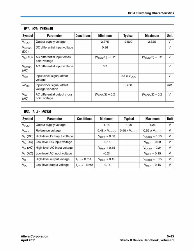
Table 5–19. SSTL-2 Class I Specifications
Symbol Parameter Conditions Minimum Typical Maximum Unit
VCCIO Output supply voltage 2.375 2.500 2.625 V
VTT Termination voltage VREF – 0.04 VREF VREF + 0.04 V
VREF Reference voltage 1.188 1.250 1.313 V
VIH (DC) High-level DC input voltage VREF + 0.18 3.00 V
VIL (DC) Low-level DC input voltage –0.30 VREF – 0.18 V
VI H (AC) High-level AC input voltage VR E F + 0.35 V
VI L (AC) Low-level AC input voltage VR E F - 0.35 V
VOH High-level output voltage IOH = –8.1 mA (1) VTT + 0.57 V
VOL Low-level output voltage IOL = 8.1 mA (1) VTT – 0.57 V
Note to Table 5–19:(1) This specification is supported across all the programmable drive settings available for this I/O standard as shown
in the Stratix II Architecture chapter in volume 1 of the Stratix II Device Handbook.
Table 5–20. SSTL-2 Class II Specifications
Symbol Parameter Conditions Minimum Typical Maximum Unit
VCCIO Output supply voltage 2.375 2.500 2.625 V
VTT Termination voltage VREF – 0.04 VREF VREF + 0.04 V
VREF Reference voltage 1.188 1.250 1.313 V
VIH (DC) High-level DC input voltage VREF + 0.18 VCCIO + 0.30 V
VIL (DC) Low-level DC input voltage –0.30 VREF – 0.18 V
VI H (AC) High-level AC input voltage VR E F + 0.35 V
VI L (AC) Low-level AC input voltage VR E F - 0.35 V
VOH High-level output voltage IOH = –16.4 mA (1) VTT + 0.76 V
VOL Low-level output voltage IOL = 16.4 mA (1) VTT – 0.76 V
Note to Table 5–20:(1) This specification is supported across all the programmable drive settings available for this I/O standard as shown
in the Stratix II Architecture chapter in volume 1 of the Stratix II Device Handbook.
Altera Corporation 5–13April 2011 Stratix II Device Handbook, Volume 1
DC & Switching Characteristics
Table 5–21. SSTL-2 Class I & II Differential Specifications
Symbol Parameter Conditions Minimum Typical Maximum Unit
VCCIO Output supply voltage 2.375 2.500 2.625 V
VSWING
(DC)DC differential input voltage 0.36 V
VX (AC) AC differential input cross point voltage
(VCCIO/2) – 0.2 (VCCIO/2) + 0.2 V
VSWING
(AC)AC differential input voltage 0.7 V
VISO Input clock signal offset voltage
0.5 × VCCIO V
ΔVISO Input clock signal offset voltage variation
±200 mV
VOX (AC)
AC differential output cross point voltage
(VCCIO/2) – 0.2 (VCCIO/2) + 0.2 V
Table 5–22. 1.2-V HSTL Specifications
Symbol Parameter Conditions Minimum Typical Maximum Unit
VCCIO Output supply voltage 1.14 1.20 1.26 V
VRE F Reference voltage 0.48 × VC C I O 0.50 × VC C I O 0.52 × VC C I O V
VIH (DC) High-level DC input voltage VR E F + 0.08 VC CI O + 0.15 V
VIL (DC) Low-level DC input voltage –0.15 VR E F – 0.08 V
VIH (AC) High-level AC input voltage VR E F + 0.15 VC CI O + 0.24 V
VIL (AC) Low-level AC input voltage –0.24 VR E F – 0.15 V
VOH High-level output voltage IO H = 8 mA VR E F + 0.15 VC CI O + 0.15 V
VOL Low-level output voltage IO H = –8 mA –0.15 VR E F – 0.15 V

5–14 Altera CorporationStratix II Device Handbook, Volume 1 April 2011
Operating Conditions
Table 5–23. 1.5-V HSTL Class I Specifications
Symbol Parameter Conditions Minimum Typical Maximum Unit
VCCIO Output supply voltage 1.425 1.500 1.575 V
VREF Input reference voltage 0.713 0.750 0.788 V
VTT Termination voltage 0.713 0.750 0.788 V
VIH (DC) DC high-level input voltage VREF + 0.1 V
VIL (DC) DC low-level input voltage –0.3 VREF – 0.1 V
VIH (AC) AC high-level input voltage VREF + 0.2 V
VIL (AC) AC low-level input voltage VREF – 0.2 V
VOH High-level output voltage IOH = 8 mA (1) VCCIO – 0.4 V
VOL Low-level output voltage IOH = –8 mA (1) 0.4 V
Note to Table 5–23:(1) This specification is supported across all the programmable drive settings available for this I/O standard as shown
in the Stratix II Architecture chapter in volume 1 of the Stratix II Device Handbook.
Table 5–24. 1.5-V HSTL Class II Specifications
Symbol Parameter Conditions Minimum Typical Maximum Unit
VCCIO Output supply voltage 1.425 1.500 1.575 V
VREF Input reference voltage 0.713 0.750 0.788 V
VTT Termination voltage 0.713 0.750 0.788 V
VIH (DC) DC high-level input voltage VREF + 0.1 V
VIL (DC) DC low-level input voltage –0.3 VREF – 0.1 V
VIH (AC) AC high-level input voltage VREF + 0.2 V
VIL (AC) AC low-level input voltage VREF – 0.2 V
VOH High-level output voltage IOH = 16 mA (1) VCCIO – 0.4 V
VOL Low-level output voltage IOH = –16 mA (1) 0.4 V
Note to Table 5–24:(1) This specification is supported across all the programmable drive settings available for this I/O standard as shown
in the Stratix II Architecture chapter in volume 1 of the Stratix II Device Handbook.
Altera Corporation 5–15April 2011 Stratix II Device Handbook, Volume 1
DC & Switching Characteristics
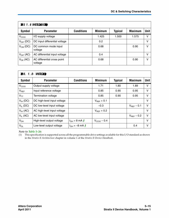
Table 5–25. 1.5-V HSTL Class I & II Differential Specifications
Symbol Parameter Conditions Minimum Typical Maximum Unit
VCCIO I/O supply voltage 1.425 1.500 1.575 V
VDIF (DC) DC input differential voltage 0.2 V
VCM (DC) DC common mode input voltage
0.68 0.90 V
VDIF (AC) AC differential input voltage 0.4 V
VOX (AC) AC differential cross point voltage
0.68 0.90 V
Table 5–26. 1.8-V HSTL Class I Specifications
Symbol Parameter Conditions Minimum Typical Maximum Unit
VCCIO Output supply voltage 1.71 1.80 1.89 V
VREF Input reference voltage 0.85 0.90 0.95 V
VTT Termination voltage 0.85 0.90 0.95 V
VIH (DC) DC high-level input voltage VREF + 0.1 V
VIL (DC) DC low-level input voltage –0.3 VREF – 0.1 V
VIH (AC) AC high-level input voltage VREF + 0.2 V
VIL (AC) AC low-level input voltage VREF – 0.2 V
VOH High-level output voltage IOH = 8 mA (1) VCCIO – 0.4 V
VOL Low-level output voltage IOH = –8 mA (1) 0.4 V
Note to Table 5–26:(1) This specification is supported across all the programmable drive settings available for this I/O standard as shown
in the Stratix II Architecture chapter in volume 1 of the Stratix II Device Handbook.

5–16 Altera CorporationStratix II Device Handbook, Volume 1 April 2011
Operating Conditions
Table 5–27. 1.8-V HSTL Class II Specifications
Symbol Parameter Conditions Minimum Typical Maximum Unit
VCCIO Output supply voltage 1.71 1.80 1.89 V
VREF Input reference voltage 0.85 0.90 0.95 V
VTT Termination voltage 0.85 0.90 0.95 V
VIH (DC) DC high-level input voltage VREF + 0.1 V
VIL (DC) DC low-level input voltage –0.3 VREF – 0.1 V
VIH (AC) AC high-level input voltage VREF + 0.2 V
VIL (AC) AC low-level input voltage VREF – 0.2 V
VOH High-level output voltage IOH = 16 mA (1) VCCIO – 0.4 V
VOL Low-level output voltage IOH = –16 mA (1) 0.4 V
Note to Table 5–27:(1) This specification is supported across all the programmable drive settings available for this I/O standard as shown
in the Stratix II Architecture chapter in volume 1 of the Stratix II Device Handbook.
Table 5–28. 1.8-V HSTL Class I & II Differential Specifications
Symbol Parameter Conditions Minimum Typical Maximum Unit
VCCIO I/O supply voltage 1.71 1.80 1.89 V
VDIF (DC) DC input differential voltage 0.2 VCCIO + 0.6 V V
VCM (DC) DC common mode input voltage
0.78 1.12 V
VDIF (AC) AC differential input voltage 0.4 VCCIO + 0.6 V V
VOX (AC) AC differential cross point voltage
0.68 0.90 V
Altera Corporation 5–17April 2011 Stratix II Device Handbook, Volume 1
DC & Switching Characteristics
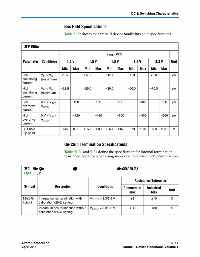
Bus Hold Specifications
Table 5–29 shows the Stratix II device family bus hold specifications.
On-Chip Termination Specifications
Tables 5–30 and 5–31 define the specification for internal termination resistance tolerance when using series or differential on-chip termination.
Table 5–29. Bus Hold Parameters
Parameter Conditions
VCCIO Level
Unit1.2 V 1.5 V 1.8 V 2.5 V 3.3 V
Min Max Min Max Min Max Min Max Min Max
Low sustaining current
VIN > VIL (maximum)
22.5 25.0 30.0 50.0 70.0 μA
High sustaining current
VIN < VIH (minimum)
–22.5 –25.0 –30.0 –50.0 –70.0 μA
Low overdrive current
0 V < VIN < VCCIO
120 160 200 300 500 μA
High overdrive current
0 V < VIN < VCCIO
–120 –160 –200 –300 –500 μA
Bus-hold trip point
0.45 0.95 0.50 1.00 0.68 1.07 0.70 1.70 0.80 2.00 V
Table 5–30. Series On-Chip Termination Specification for Top & Bottom I/O Banks (Part 1 of 2)Notes (1), 2
Symbol Description Conditions
Resistance Tolerance
Commercial Max
Industrial Max Unit
25-Ω RS 3.3/2.5
Internal series termination with calibration (25-Ω setting)
VC CI O = 3.3/2.5 V ±5 ±10 %
Internal series termination without calibration (25-Ω setting)
VC CI O = 3.3/2.5 V ±30 ±30 %

5–18 Altera CorporationStratix II Device Handbook, Volume 1 April 2011
Operating Conditions
50-Ω RS 3.3/2.5
Internal series termination with calibration (50-Ω setting)
VC CI O = 3.3/2.5 V ±5 ±10 %
Internal series termination without calibration (50-Ω setting)
VC CI O = 3.3/2.5 V ±30 ±30 %
50-Ω RT 2.5
Internal parallel termination with calibration (50-Ω setting)
VC CI O = 1.8 V ±30 ±30 %
25-Ω RS 1.8
Internal series termination with calibration (25-Ω setting)
VC CI O = 1.8 V ±5 ±10 %
Internal series termination without calibration (25-Ω setting)
VC CI O = 1.8 V ±30 ±30 %
50-Ω RS 1.8
Internal series termination with calibration (50-Ω setting)
VC CI O = 1.8 V ±5 ±10 %
Internal series termination without calibration (50-Ω setting)
VC CI O = 1.8 V ±30 ±30 %
50-Ω RT 1.8
Internal parallel termination with calibration (50-Ω setting)
VC CI O = 1.8 V ±10 ±15 %
50−Ω RS 1.5
Internal series termination with calibration (50-Ω setting)
VC CI O = 1.5 V ±8 ±10 %
Internal series termination without calibration (50-Ω setting)
VC CI O = 1.5 V ±36 ±36 %
50-Ω RT 1.5
Internal parallel termination with calibration (50-Ω setting)
VC CI O = 1.5 V ±10 ±15 %
50−Ω RS 1.2
Internal series termination with calibration (50-Ω setting)
VC CI O = 1.2 V ±8 ±10 %
Internal series termination without calibration (50-Ω setting)
VC CI O = 1.2 V ±50 ±50 %
50-Ω RT 1.2
Internal parallel termination with calibration (50-Ω setting)
VC CI O = 1.2 V ±10 ±15 %
Notes for Table 5–30:(1) The resistance tolerances for calibrated SOCT and POCT are for the moment of calibration. If the temperature or
voltage changes over time, the tolerance may also change.(2) On-chip parallel termination with calibration is only supported for input pins.
Table 5–30. Series On-Chip Termination Specification for Top & Bottom I/O Banks (Part 2 of 2)Notes (1), 2
Symbol Description Conditions
Resistance Tolerance
Commercial Max
Industrial Max Unit

Altera Corporation 5–19April 2011 Stratix II Device Handbook, Volume 1
DC & Switching Characteristics
Pin Capacitance
Table 5–32 shows the Stratix II device family pin capacitance.
Table 5–31. Series & Differential On-Chip Termination Specification for Left & Right I/O Banks
Symbol Description Conditions
Resistance Tolerance
Commercial Max
Industrial Max Unit
25-Ω RS 3.3/2.5
Internal series termination without calibration (25-Ω setting)
VC CI O = 3.3/2.5 V ±30 ±30 %
50-Ω RS 3.3/2.5/1.8
Internal series termination without calibration (50-Ω setting)
VC CI O = 3.3/2.5/1.8 V ±30 ±30 %
50-Ω RS 1.5 Internal series termination without calibration (50-Ω setting)
VC CI O = 1.5 V ±36 ±36 %
RD Internal differential termination for LVDS or HyperTransport technology (100-Ω setting)
VC CI O = 2.5 V ±20 ±25 %
Table 5–32. Stratix II Device Capacitance Note (1)
Symbol Parameter Typical Unit
CI OT B Input capacitance on I/O pins in I/O banks 3, 4, 7, and 8. 5.0 pF
CI O L R Input capacitance on I/O pins in I/O banks 1, 2, 5, and 6, including high-speed differential receiver and transmitter pins.
6.1 pF
CC L K T B Input capacitance on top/bottom clock input pins: CLK[4..7] and CLK[12..15].
6.0 pF
CC L K L R Input capacitance on left/right clock inputs: CLK0, CLK2, CLK8, CLK10. 6.1 pF
CC L K L R + Input capacitance on left/right clock inputs: CLK1, CLK3, CLK9, and CLK11.
3.3 pF
CO U T F B Input capacitance on dual-purpose clock output/feedback pins in PLL banks 9, 10, 11, and 12.
6.7 pF
Note to Table 5–32:(1) Capacitance is sample-tested only. Capacitance is measured using time-domain reflections (TDR). Measurement
accuracy is within ±0.5pF

5–20 Altera CorporationStratix II Device Handbook, Volume 1 April 2011
Power Consumption
Power Consumption
Altera® offers two ways to calculate power for a design: the Excel-based PowerPlay Early Power Estimator power calculator and the Quartus® II PowerPlay Power Analyzer feature.
The interactive Excel-based PowerPlay Early Power Estimator is typically used prior to designing the FPGA in order to get an estimate of device power. The Quartus II PowerPlay Power Analyzer provides better quality estimates based on the specifics of the design after place-and-route is complete. The Power Analyzer can apply a combination of user-entered, simulation-derived and estimated signal activities which, combined with detailed circuit models, can yield very accurate power estimates.
In both cases, these calculations should only be used as an estimation of power, not as a specification.
f For more information about PowerPlay tools, refer to the PowerPlay Early Power Estimator User Guide and the PowerPlay Early Power Estimator and PowerPlay Power Analyzer chapters in volume 3 of the Quartus II Handbook.
The PowerPlay Early Power Estimator is available on the Altera web site at www.altera.com. See Table 5–4 on page 5–3 for typical ICC standby specifications.
Timing Model The DirectDriveTM technology and MultiTrackTM interconnect ensure predictable performance, accurate simulation, and accurate timing analysis across all Stratix II device densities and speed grades. This section describes and specifies the performance, internal timing, external timing, and PLL, high-speed I/O, external memory interface, and JTAG timing specifications.
All specifications are representative of worst-case supply voltage and junction temperature conditions.
1 The timing numbers listed in the tables of this section are extracted from the Quartus II software version 5.0 SP1.
Preliminary & Final Timing
Timing models can have either preliminary or final status. The Quartus II software issues an informational message during the design compilation if the timing models are preliminary. Table 5–33 shows the status of the Stratix II device timing models.

Altera Corporation 5–21April 2011 Stratix II Device Handbook, Volume 1
DC & Switching Characteristics
Preliminary status means the timing model is subject to change. Initially, timing numbers are created using simulation results, process data, and other known parameters. These tests are used to make the preliminary numbers as close to the actual timing parameters as possible.
Final timing numbers are based on actual device operation and testing. These numbers reflect the actual performance of the device under worst-case voltage and junction temperature conditions.
I/O Timing Measurement Methodology
Altera characterizes timing delays at the worst-case process, minimum voltage, and maximum temperature for input register setup time (tSU) and hold time (tH). The Quartus II software uses the following equations to calculate tSU and tH timing for Stratix II devices input signals.
tSU = + data delay from input pin to input register+ micro setup time of the input register– clock delay from input pin to input register
tH = – data delay from input pin to input register+ micro hold time of the input register+ clock delay from input pin to input register
Figure 5–3 shows the setup and hold timing diagram for input registers.
Table 5–33. Stratix II Device Timing Model Status
Device Preliminary Final
EP2S15 v
EP2S30 v
EP2S60 v
EP2S90 v
EP2S130 v
EP2S180 v

5–22 Altera CorporationStratix II Device Handbook, Volume 1 April 2011
Timing Model
Figure 5–3. Input Register Setup & Hold Timing Diagram
For output timing, different I/O standards require different baseline loading techniques for reporting timing delays. Altera characterizes timing delays with the required termination for each I/O standard and with 0 pF (except for PCI and PCI-X which use 10 pF) loading and the timing is specified up to the output pin of the FPGA device. The Quartus II software calculates the I/O timing for each I/O standard with a default baseline loading as specified by the I/O standards.
The following measurements are made during device characterization. Altera measures clock-to-output delays (tCO) at worst-case process, minimum voltage, and maximum temperature (PVT) for default loading conditions shown in Table 5–34. Use the following equations to calculate clock pin to output pin timing for Stratix II devices.
tCO from clock pin to I/O pin = delay from clock pad to I/O output register + IOE output register clock-to-output delay + delay from output register to output pin + I/O output delay
txz/tzx from clock pin to I/O pin = delay from clock pad to I/O output register + IOE output register clock-to-output delay + delay from output register to output pin + I/O output delay + output enable pin delay
Simulation using IBIS models is required to determine the delays on the PCB traces in addition to the output pin delay timing reported by the Quartus II software and the timing model in the device handbook.
1. Simulate the output driver of choice into the generalized test setup, using values from Table 5–34.
2. Record the time to VMEAS.
3. Simulate the output driver of choice into the actual PCB trace and load, using the appropriate IBIS model or capacitance value to represent the load.
Input Data Delay
Input Clock Delay
micro tSUmicro tH

Altera Corporation 5–23April 2011 Stratix II Device Handbook, Volume 1
DC & Switching Characteristics
4. Record the time to VMEAS.
5. Compare the results of steps 2 and 4. The increase or decrease in delay should be added to or subtracted from the I/O Standard Output Adder delays to yield the actual worst-case propagation delay (clock-to-output) of the PCB trace.
The Quartus II software reports the timing with the conditions shown in Table 5–34 using the above equation. Figure 5–4 shows the model of the circuit that is represented by the output timing of the Quartus II software.
Figure 5–4. Output Delay Timing Reporting Setup Modeled by Quartus II
Notes to Figure 5–4:(1) Output pin timing is reported at the output pin of the FPGA device. Additional
delays for loading and board trace delay need to be accounted for with IBIS model simulations.
(2) VCCPD is 3.085 V unless otherwise specified.(3) VCCINT is 1.12 V unless otherwise specified.
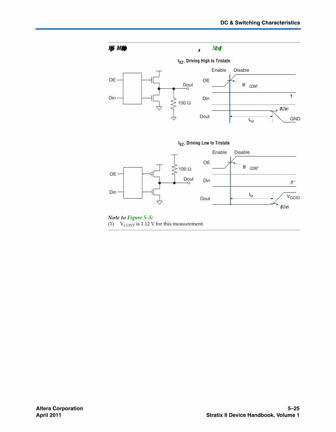
Figures 5–5 and 5–6 show the measurement setup for output disable and output enable timing.
OutputBuffer
VTTVCCIO
RDOutputn
OutputpRT
CL
RS
VMEAS
Output
GND GND

5–24 Altera CorporationStratix II Device Handbook, Volume 1 April 2011
Timing Model
Table 5–34. Output Timing Measurement Methodology for Output Pins Notes (1), (2), (3)
I/O StandardLoading and Termination Measurement
Point
RS (Ω) RD (Ω) RT (Ω) VCCIO (V) VTT (V) CL (pF) VMEAS (V)
LVTTL (4) 3.135 0 1.5675
LVCMOS (4) 3.135 0 1.5675
2.5 V (4) 2.375 0 1.1875
1.8 V (4) 1.710 0 0.855
1.5 V (4) 1.425 0 0.7125
PCI (5) 2.970 10 1.485
PCI-X (5) 2.970 10 1.485
SSTL-2 Class I 25 50 2.325 1.123 0 1.1625
SSTL-2 Class II 25 25 2.325 1.123 0 1.1625
SSTL-18 Class I 25 50 1.660 0.790 0 0.83
SSTL-18 Class II 25 25 1.660 0.790 0 0.83
1.8-V HSTL Class I 50 50 1.660 0.790 0 0.83
1.8-V HSTL Class II 25 25 1.660 0.790 0 0.83
1.5-V HSTL Class I 50 50 1.375 0.648 0 0.6875
1.5-V HSTL Class II 25 1.375 0.648 0 0.6875
1.2-V HSTL with OCT 50 1.140 0 0.570
Differential SSTL-2 Class I 50 50 2.325 1.123 0 1.1625
Differential SSTL-2 Class II 25 25 2.325 1.123 0 1.1625
Differential SSTL-18 Class I 50 50 1.660 0.790 0 0.83
Differential SSTL-18 Class II 25 25 1.660 0.790 0 0.83
1.5-V Differential HSTL Class I 50 50 1.375 0.648 0 0.6875
1.5-V Differential HSTL Class II 25 1.375 0.648 0 0.6875
1.8-V Differential HSTL Class I 50 50 1.660 0.790 0 0.83
1.8-V Differential HSTL Class II 25 25 1.660 0.790 0 0.83
LVDS 100 2.325 0 1.1625
HyperTransport 100 2.325 0 1.1625
LVPECL 100 3.135 0 1.5675
Notes to Table 5–34:(1) Input measurement point at internal node is 0.5 × VCCINT.(2) Output measuring point for VMEAS at buffer output is 0.5 × VCCIO.(3) Input stimulus edge rate is 0 to VCC in 0.2 ns (internal signal) from the driver preceding the I/O buffer.(4) Less than 50-mV ripple on VCCIO and VCCPD, VCCINT = 1.15 V with less than 30-mV ripple(5) VCCPD = 2.97 V, less than 50-mV ripple on VCCIO and VCCPD, VCCINT = 1.15 V
Altera Corporation 5–25April 2011 Stratix II Device Handbook, Volume 1
DC & Switching Characteristics
Figure 5–5. Measurement Setup for txz Note (1)
Note to Figure 5–5:(1) VCCINT is 1.12 V for this measurement.
tXZ, Driving High to Tristate
tXZ, Driving Low to Tristate
100 Ω
Din
OEDout
VCCIO
OE
Enable Disable
Dout
Din
tlz
100 mv
½ VCCINT
“0”
100 ΩDin
OEDout
OE
Enable Disable
Dout
Din
thz
100 mv
½ VCCINT
“1”
GND
5–26 Altera CorporationStratix II Device Handbook, Volume 1 April 2011
Timing Model
Figure 5–6. Measurement Setup for tzx
Table 5–35 specifies the input timing measurement setup.
tZX, Tristate to Driving High
tZX, Tristate to Driving Low
1 MΩ
Din
OEDout
1 MΩDin
OEDout
OE
Disable Enable
Dout
Din
tzh
½ VCCINT
“1”
½ VCCIO
OE
Disable Enable
Dout
Din
½ VCCINT
“0”
tzl ½ VCCIO
Table 5–35. Timing Measurement Methodology for Input Pins (Part 1 of 2) Notes (1)–(4)
I/O StandardMeasurement Conditions Measurement Point
VCCIO (V) VREF (V) Edge Rate (ns) VM E A S (V)
LVTTL (5) 3.135 3.135 1.5675
LVCMOS (5) 3.135 3.135 1.5675
2.5 V (5) 2.375 2.375 1.1875
1.8 V (5) 1.710 1.710 0.855
1.5 V (5) 1.425 1.425 0.7125
PCI (6) 2.970 2.970 1.485
PCI-X (6) 2.970 2.970 1.485
SSTL-2 Class I 2.325 1.163 2.325 1.1625
SSTL-2 Class II 2.325 1.163 2.325 1.1625
SSTL-18 Class I 1.660 0.830 1.660 0.83
SSTL-18 Class II 1.660 0.830 1.660 0.83
1.8-V HSTL Class I 1.660 0.830 1.660 0.83
Altera Corporation 5–27April 2011 Stratix II Device Handbook, Volume 1
DC & Switching Characteristics
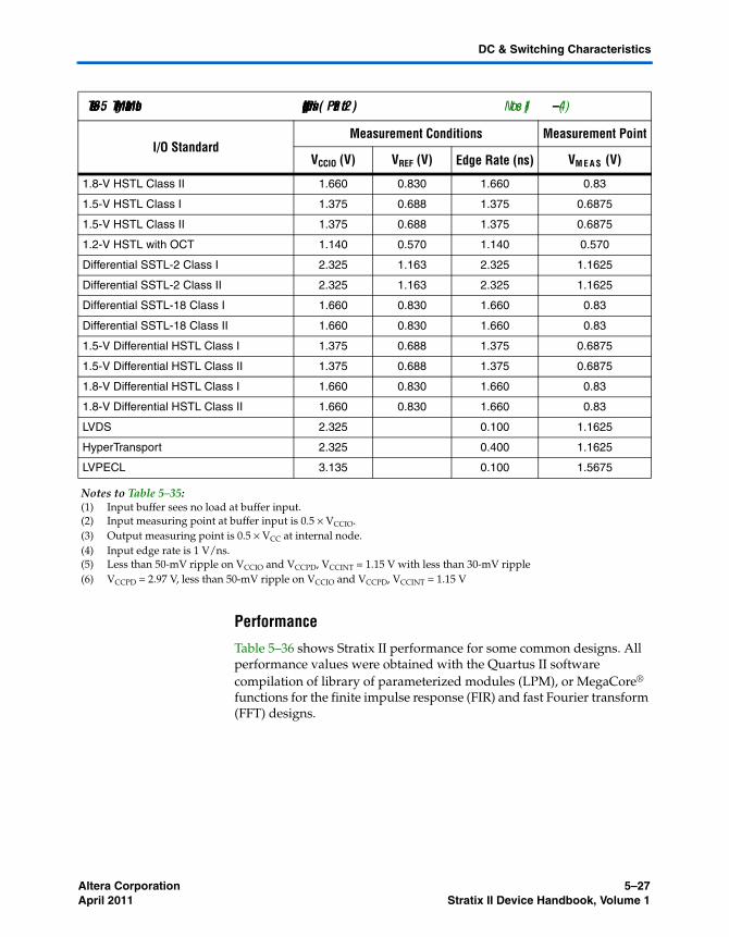
Performance
Table 5–36 shows Stratix II performance for some common designs. All performance values were obtained with the Quartus II software compilation of library of parameterized modules (LPM), or MegaCore® functions for the finite impulse response (FIR) and fast Fourier transform (FFT) designs.
1.8-V HSTL Class II 1.660 0.830 1.660 0.83
1.5-V HSTL Class I 1.375 0.688 1.375 0.6875
1.5-V HSTL Class II 1.375 0.688 1.375 0.6875
1.2-V HSTL with OCT 1.140 0.570 1.140 0.570
Differential SSTL-2 Class I 2.325 1.163 2.325 1.1625
Differential SSTL-2 Class II 2.325 1.163 2.325 1.1625
Differential SSTL-18 Class I 1.660 0.830 1.660 0.83
Differential SSTL-18 Class II 1.660 0.830 1.660 0.83
1.5-V Differential HSTL Class I 1.375 0.688 1.375 0.6875
1.5-V Differential HSTL Class II 1.375 0.688 1.375 0.6875
1.8-V Differential HSTL Class I 1.660 0.830 1.660 0.83
1.8-V Differential HSTL Class II 1.660 0.830 1.660 0.83
LVDS 2.325 0.100 1.1625
HyperTransport 2.325 0.400 1.1625
LVPECL 3.135 0.100 1.5675
Notes to Table 5–35:(1) Input buffer sees no load at buffer input.(2) Input measuring point at buffer input is 0.5 × VCCIO.(3) Output measuring point is 0.5 × VCC at internal node.(4) Input edge rate is 1 V/ns.(5) Less than 50-mV ripple on VCCIO and VCCPD, VCCINT = 1.15 V with less than 30-mV ripple(6) VCCPD = 2.97 V, less than 50-mV ripple on VCCIO and VCCPD, VCCINT = 1.15 V
Table 5–35. Timing Measurement Methodology for Input Pins (Part 2 of 2) Notes (1)–(4)
I/O StandardMeasurement Conditions Measurement Point
VCCIO (V) VREF (V) Edge Rate (ns) VM E A S (V)

5–28 Altera CorporationStratix II Device Handbook, Volume 1 April 2011
Timing Model
1 The performance numbers in Table 5–36 are extracted from the Quartus II software version 5.1 SP1.
Table 5–36. Stratix II Performance Notes (Part 1 of 6) Note (1)
Applications
Resources Used Performance
ALUTsTriMatrix Memory Blocks
DSP Blocks
-3 Speed Grade
(2)
-3 Speed Grade
(3)
-4 Speed Grade
-5 Speed Grade
Unit
LE 16-to-1 multiplexer (4) 21 0 0 654.87 625.0 523.83 460.4 MHz
32-to-1 multiplexer (4) 38 0 0 519.21 473.26 464.25 384.17 MHz
16-bit counter 16 0 0 566.57 538.79 489.23 421.05 MHz
64-bit counter 64 0 0 244.31 232.07 209.11 181.38 MHz
TriMatrix Memory M512 block
Simple dual-port RAM 32 × 18 bit
0 1 0 500.00 476.19 434.02 373.13 MHz
FIFO 32 x 18 bit 22 1 0 500.00 476.19 434.78 373.13 MHz
TriMatrix Memory M4K block
Simple dual-port RAM 128 x 36 bit (8)
0 1 0 540.54 515.46 469.48 401.60 MHz
True dual-port RAM 128 × 18 bit (8)
0 1 0 540.54 515.46 469.48 401.60 MHz
FIFO 128 × 36 bit
22 1 0 530.22 499.00 469.48 401.60 MHz
Simple dual-port RAM 128 × 36 bit (9)
0 1 0 475.28 453.30 413.22 354.10 MHz
True dual-port RAM 128 × 18 bit (9)
0 1 0 475.28 453.30 413.22 354.10 MHz

Altera Corporation 5–29April 2011 Stratix II Device Handbook, Volume 1
DC & Switching Characteristics
TriMatrix Memory M-RAM block
Single port RAM 4K × 144 bit
0 1 0 349.65 333.33 303.95 261.09 MHz
Simple dual-port RAM 4K × 144 bit
0 1 0 420.16 400.00 364.96 313.47 MHz
True dual-port RAM 4K × 144 bit
0 1 0 349.65 333.33 303.95 261.09 MHz
Single port RAM 8K × 72 bit
0 1 0 354.60 337.83 307.69 263.85 MHz
Simple dual-port RAM 8K × 72 bit
0 1 0 420.16 400.00 364.96 313.47 MHz
True dual-portRAM 8K × 72 bit
0 1 0 349.65 333.33 303.95 261.09 MHz
Single portRAM 16K × 36 bit
0 1 0 364.96 347.22 317.46 271.73 MHz
Simple dual-portRAM 16K × 36 bit
0 1 0 420.16 400.00 364.96 313.47 MHz
True dual-port RAM 16K × 36 bit
0 1 0 359.71 342.46 313.47 268.09 MHz
Single portRAM 32K × 18 bit
0 1 0 364.96 347.22 317.46 271.73 MHz
Simple dual-port RAM 32K × 18 bit
0 1 0 420.16 400.0 364.96 313.47 MHz
True dual-port RAM 32K × 18 bit
0 1 0 359.71 342.46 313.47 268.09 MHz
Single port RAM 64K × 9 bit
0 1 0 364.96 347.22 317.46 271.73 MHz
Simple dual-port RAM 64K × 9 bit
0 1 0 420.16 400.0 364.96 313.47 MHz
True dual-port RAM 64K × 9 bit
0 1 0 359.71 342.46 313.47 268.09 MHz
Table 5–36. Stratix II Performance Notes (Part 2 of 6) Note (1)
Applications
Resources Used Performance
ALUTsTriMatrix Memory Blocks
DSP Blocks
-3 Speed Grade
(2)
-3 Speed Grade
(3)
-4 Speed Grade
-5 Speed Grade
Unit

5–30 Altera CorporationStratix II Device Handbook, Volume 1 April 2011
Timing Model
DSP block
9 × 9-bit multiplier (5) 0 0 1 430.29 409.16 373.13 320.10 MHz
18 × 18-bit multiplier (5)
0 0 1 410.17 390.01 356.12 305.06 MHz
18 × 18-bit multiplier (7)
0 0 1 450.04 428.08 391.23 335.12 MHz
36 × 36-bit multiplier (5)
0 0 1 250.00 238.15 217.48 186.60 MHz
36 × 36-bit multiplier (6)
0 0 1 410.17 390.01 356.12 305.06 MHz
18-bit, four-tap FIR filter
0 0 1 410.17 390.01 356.12 305.06 MHz
Larger designs
8-bit,16-tap parallel FIR filter
58 0 4 259.06 240.61 217.15 185.01 MHz
8-bit, 1024-point, streaming, three multipliers and five adders FFT function
2976 22 9 398.72 364.03 355.23 306.37 MHz
8-bit, 1024-point, streaming, four multipliers and two adders FFT function
2781 22 12 398.56 409.16 347.22 311.13 MHz
8-bit, 1024-point, single output, one parallel FFT engine, burst, three multipliers and five adders FFT function
984 5 3 425.17 365.76 346.98 292.39 MHz
8-bit, 1024-point, single output, one parallel FFT engine, burst, four multipliers and two adders FFT function
919 5 4 427.53 378.78 357.14 307.59 MHz
Table 5–36. Stratix II Performance Notes (Part 3 of 6) Note (1)
Applications
Resources Used Performance
ALUTsTriMatrix Memory Blocks
DSP Blocks
-3 Speed Grade
(2)
-3 Speed Grade
(3)
-4 Speed Grade
-5 Speed Grade
Unit

Altera Corporation 5–31April 2011 Stratix II Device Handbook, Volume 1
DC & Switching Characteristics
Larger designs
8-bit, 1024-point, single output, two parallel FFT engines, burst, three multiplier and five adders FFT function
1725 10 6 430.29 401.92 373.13 319.08 MHz
8-bit, 1024-point, single output, two parallel FFT engines, burst, four multipliers and two adders FFT function
1594 10 8 422.65 407.33 373.13 329.10 MHz
8-bit, 1024-point, quadrant output, one parallel FFT engine, burst, three multipliers and five adders FFT function
2361 10 9 315.45 342.81 325.73 284.25 MHz
8-bit, 1024-point, quadrant output, one parallel FFT engine, burst, four multipliers and two adders FFT function
2165 10 12 373.13 369.54 317.96 256.14 MHz
8-bit, 1024-point, quadrant output, two parallel FFT engines, burst, three multipliers and five adders FFT function
3996 14 18 378.50 367.10 332.33 288.68 MHz
8-bit, 1024-point, quadrant output, two parallel FFT engines, burst, four multipliers and two adders FFT function
3604 14 24 391.38 361.14 340.25 280.89 MHz
Table 5–36. Stratix II Performance Notes (Part 4 of 6) Note (1)
Applications
Resources Used Performance
ALUTsTriMatrix Memory Blocks
DSP Blocks
-3 Speed Grade
(2)
-3 Speed Grade
(3)
-4 Speed Grade
-5 Speed Grade
Unit
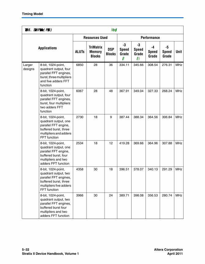
5–32 Altera CorporationStratix II Device Handbook, Volume 1 April 2011
Timing Model
Larger designs
8-bit, 1024-point, quadrant output, four parallel FFT engines, burst, three multipliers and five adders FFT function
6850 28 36 334.11 345.66 308.54 276.31 MHz
8-bit, 1024-point, quadrant output, four parallel FFT engines, burst, four multipliers two adders FFT function
6067 28 48 367.91 349.04 327.33 268.24 MHz
8-bit, 1024-point, quadrant output, one parallel FFT engine, buffered burst, three multipliers and adders FFT function
2730 18 9 387.44 388.34 364.56 306.84 MHz
8-bit, 1024-point, quadrant output, one parallel FFT engine, buffered burst, four multipliers and two adders FFT function
2534 18 12 419.28 369.66 364.96 307.88 MHz
8-bit, 1024-point, quadrant output, two parallel FFT engines, buffered burst, three multipliers five adders FFT function
4358 30 18 396.51 378.07 340.13 291.29 MHz
8-bit, 1024-point, quadrant output, two parallel FFT engines, buffered burst four multipliers and two adders FFT function
3966 30 24 389.71 398.08 356.53 280.74 MHz
Table 5–36. Stratix II Performance Notes (Part 5 of 6) Note (1)
Applications
Resources Used Performance
ALUTsTriMatrix Memory Blocks
DSP Blocks
-3 Speed Grade
(2)
-3 Speed Grade
(3)
-4 Speed Grade
-5 Speed Grade
Unit

Altera Corporation 5–33April 2011 Stratix II Device Handbook, Volume 1
DC & Switching Characteristics
Larger designs
8-bit, 1024-point, quadrant output, four parallel FFT engines, buffered burst, three multipliers five adders FFT function
7385 60 36 359.58 352.98 312.01 278.00 MHz
8-bit, 1024-point, quadrant output, four parallel FFT engines, buffered burst, four multipliers and two adders FFT function
6601 60 48 371.88 355.74 327.86 277.62 MHz
Notes for Table 5–36:(1) These design performance numbers were obtained using the Quartus II software version 5.0 SP1.(2) These numbers apply to -3 speed grade EP2S15, EP2S30, EP2S60, and EP2S90 devices.(3) These numbers apply to -3 speed grade EP2S130 and EP2S180 devices.(4) This application uses registered inputs and outputs.(5) This application uses registered multiplier input and output stages within the DSP block.(6) This application uses registered multiplier input, pipeline, and output stages within the DSP block.(7) This application uses registered multiplier input with output of the multiplier stage feeding the accumulator or
subtractor within the DSP block.(8) This application uses the same clock source that is globally routed and connected to ports A and B.(9) This application uses locally routed clocks or differently sourced clocks for ports A and B.
Table 5–36. Stratix II Performance Notes (Part 6 of 6) Note (1)
Applications
Resources Used Performance
ALUTsTriMatrix Memory Blocks
DSP Blocks
-3 Speed Grade
(2)
-3 Speed Grade
(3)
-4 Speed Grade
-5 Speed Grade
Unit
5–34 Altera CorporationStratix II Device Handbook, Volume 1 April 2011
Timing Model
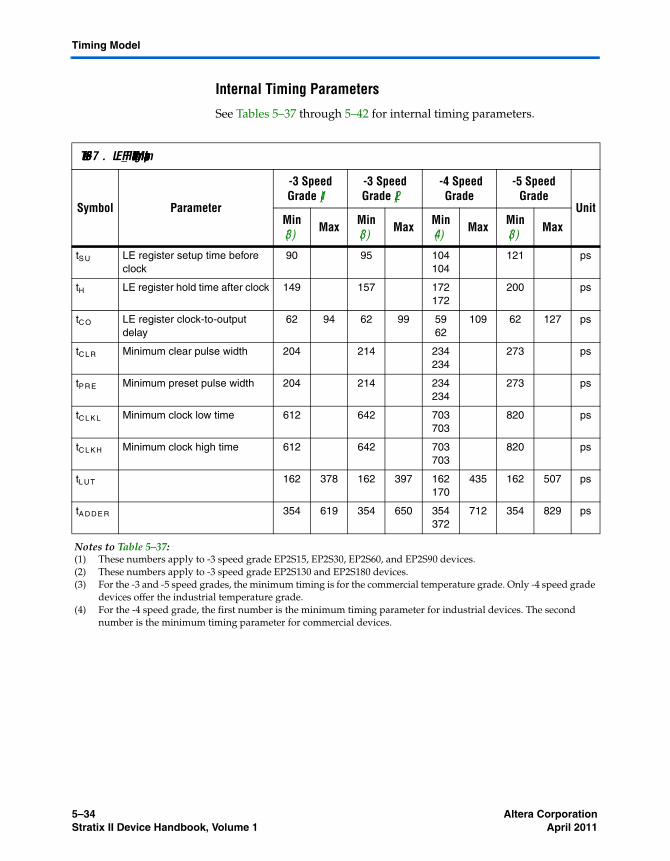
Internal Timing Parameters
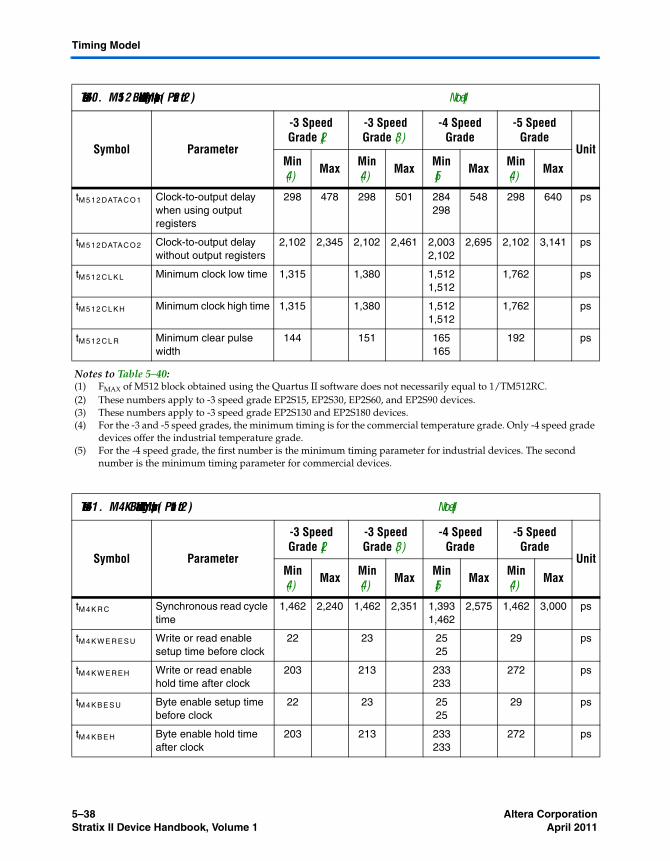
See Tables 5–37 through 5–42 for internal timing parameters.
Table 5–37. LE_FF Internal Timing Microparameters
Symbol Parameter
-3 Speed Grade (1)
-3 Speed Grade (2)
-4 Speed Grade
-5 Speed Grade
UnitMin (3) Max Min
(3) Max Min (4) Max Min
(3) Max
tS U LE register setup time before clock
90 95 104104
121 ps
tH LE register hold time after clock 149 157 172172
200 ps
tC O LE register clock-to-output delay
62 94 62 99 5962
109 62 127 ps
tC L R Minimum clear pulse width 204 214 234234
273 ps
tP R E Minimum preset pulse width 204 214 234234
273 ps
tC L K L Minimum clock low time 612 642 703703
820 ps
tC L K H Minimum clock high time 612 642 703703
820 ps
tL U T 162 378 162 397 162170
435 162 507 ps
tA D D E R 354 619 354 650 354372
712 354 829 ps
Notes to Table 5–37:(1) These numbers apply to -3 speed grade EP2S15, EP2S30, EP2S60, and EP2S90 devices.(2) These numbers apply to -3 speed grade EP2S130 and EP2S180 devices.(3) For the -3 and -5 speed grades, the minimum timing is for the commercial temperature grade. Only -4 speed grade
devices offer the industrial temperature grade.(4) For the -4 speed grade, the first number is the minimum timing parameter for industrial devices. The second
number is the minimum timing parameter for commercial devices.
Altera Corporation 5–35April 2011 Stratix II Device Handbook, Volume 1
DC & Switching Characteristics
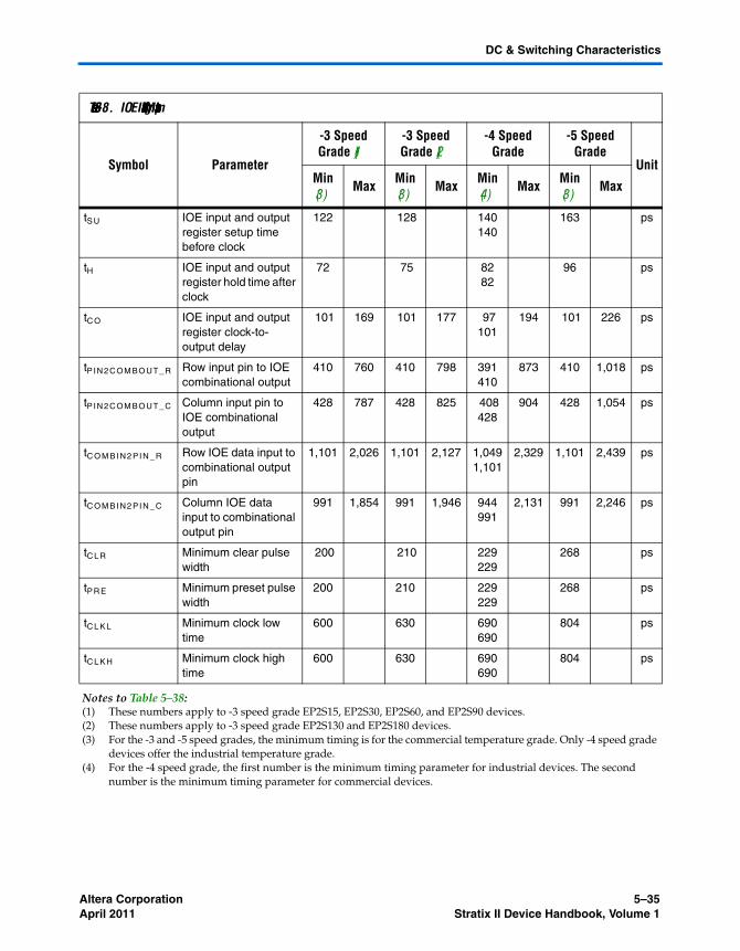
Table 5–38. IOE Internal Timing Microparameters
Symbol Parameter
-3 Speed Grade (1)
-3 Speed Grade (2)
-4 Speed Grade
-5 Speed Grade
UnitMin (3) Max Min
(3) Max Min (4) Max Min
(3) Max
tS U IOE input and output register setup time before clock
122 128 140140
163 ps
tH IOE input and output register hold time after clock
72 75 8282
96 ps
tC O IOE input and output register clock-to-output delay
101 169 101 177 97101
194 101 226 ps
tP IN 2C O M BO UT _R Row input pin to IOE combinational output
410 760 410 798 391410
873 410 1,018 ps
tP IN 2C O M BO UT _C Column input pin to IOE combinational output
428 787 428 825 408428
904 428 1,054 ps
tC O M B I N2 P I N _ R Row IOE data input to combinational output pin
1,101 2,026 1,101 2,127 1,0491,101
2,329 1,101 2,439 ps
tC O M B I N2 P I N _ C Column IOE data input to combinational output pin
991 1,854 991 1,946 944991
2,131 991 2,246 ps
tC L R Minimum clear pulse width
200 210 229229
268 ps
tP R E Minimum preset pulse width
200 210 229229
268 ps
tC L K L Minimum clock low time
600 630 690690
804 ps
tC L K H Minimum clock high time
600 630 690690
804 ps
Notes to Table 5–38:(1) These numbers apply to -3 speed grade EP2S15, EP2S30, EP2S60, and EP2S90 devices.(2) These numbers apply to -3 speed grade EP2S130 and EP2S180 devices.(3) For the -3 and -5 speed grades, the minimum timing is for the commercial temperature grade. Only -4 speed grade
devices offer the industrial temperature grade.(4) For the -4 speed grade, the first number is the minimum timing parameter for industrial devices. The second
number is the minimum timing parameter for commercial devices.

5–36 Altera CorporationStratix II Device Handbook, Volume 1 April 2011
Timing Model
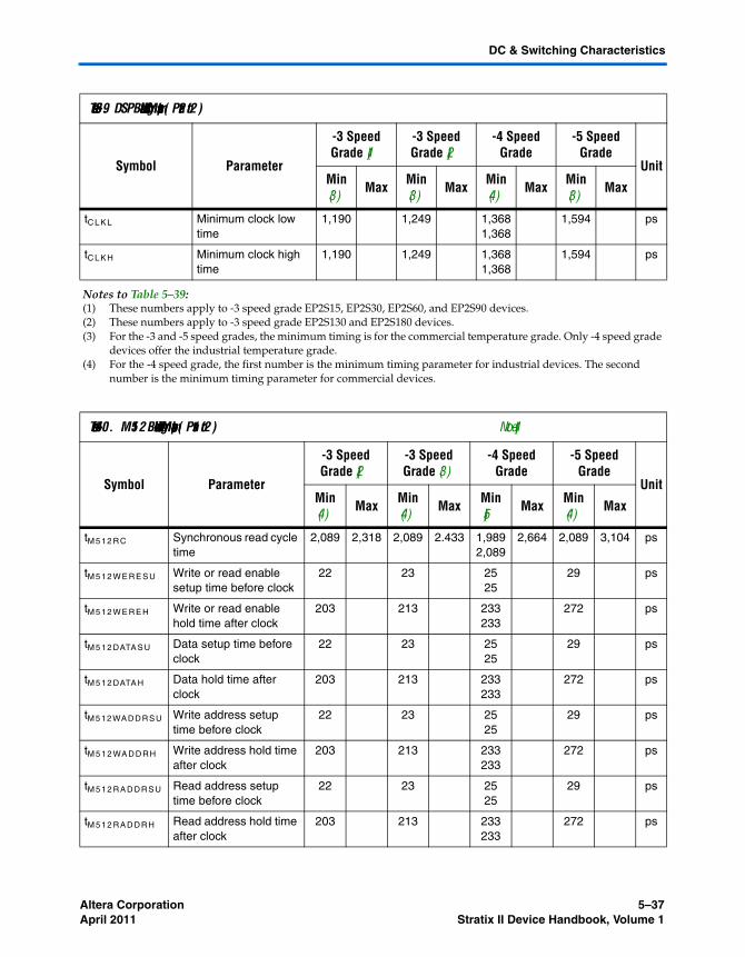
Table 5–39. DSP Block Internal Timing Microparameters (Part 1 of 2)
Symbol Parameter
-3 Speed Grade (1)
-3 Speed Grade (2)
-4 Speed Grade
-5 Speed Grade
UnitMin (3) Max Min
(3) Max Min (4) Max Min
(3) Max
tS U Input, pipeline, and output register setup time before clock
50 52 5757
67 ps
tH Input, pipeline, and output register hold time after clock
180 189 206206
241 ps
tC O Input, pipeline, and output register clock-to-output delay
0 0 0 0 00
0 0 0 ps
tI N R E G 2 P I P E 9 Input register to DSP block pipeline register in 9 × 9-bit mode
1,312 2,030 1,312 2,030 1,2501,312
2,334 1,312 2,720 ps
tI N R E G 2 P I P E 1 8 Input register to DSP block pipeline register in 18 × 18-bit mode
1,302 2,010 1,302 2,110 1,2401,302
2,311 1,302 2,693 ps
tI N R E G 2 P I P E 3 6 Input register to DSP block pipeline register in 36 × 36-bit mode
1,302 2,010 1,302 2,110 1,2401,302
2,311 1,302 2,693 ps
tP I P E 2 O U T R E G 2 A D D DSP block pipeline register to output register delay in two-multipliers adder mode
924 1,450 924 1,522 880924
1,667 924 1,943 ps
tP I P E 2 O U T R E G 4 A D D DSP block pipeline register to output register delay in four-multipliers adder mode
1,134 1,850 1,134 1,942 1,0801,134
2,127 1,134 2,479 ps
tP D 9 Combinational input to output delay for 9 × 9
2,100 2,880 2,100 3,024 2,0002,100
3,312 2,100 3,859 ps
tP D 1 8 Combinational input to output delay for 18 × 18
2,110 2,990 2,110 3,139 2,0102,110
3,438 2,110 4,006 ps
tP D 3 6 Combinational input to output delay for 36 × 36
2,939 4,450 2,939 4,672 2,8002,939
5,117 2,939 5,962 ps
tC L R Minimum clear pulse width
2,212 2,322 2,5432,543
2,964 ps
Altera Corporation 5–37April 2011 Stratix II Device Handbook, Volume 1
DC & Switching Characteristics
tC L K L Minimum clock low time
1,190 1,249 1,3681,368
1,594 ps
tC L K H Minimum clock high time
1,190 1,249 1,3681,368
1,594 ps
Notes to Table 5–39:(1) These numbers apply to -3 speed grade EP2S15, EP2S30, EP2S60, and EP2S90 devices.(2) These numbers apply to -3 speed grade EP2S130 and EP2S180 devices.(3) For the -3 and -5 speed grades, the minimum timing is for the commercial temperature grade. Only -4 speed grade
devices offer the industrial temperature grade.(4) For the -4 speed grade, the first number is the minimum timing parameter for industrial devices. The second
number is the minimum timing parameter for commercial devices.
Table 5–40. M512 Block Internal Timing Microparameters (Part 1 of 2) Note (1)
Symbol Parameter
-3 Speed Grade (2)
-3 Speed Grade (3)
-4 Speed Grade
-5 Speed Grade
UnitMin (4) Max Min
(4) Max Min (5) Max Min
(4) Max
tM 5 1 2 R C Synchronous read cycle time
2,089 2,318 2,089 2.433 1,9892,089
2,664 2,089 3,104 ps
tM 5 1 2 W E R E S U Write or read enable setup time before clock
22 23 2525
29 ps
tM 5 1 2 W E R E H Write or read enable hold time after clock
203 213 233233
272 ps
tM 5 1 2 DATA S U Data setup time before clock
22 23 2525
29 ps
tM 5 1 2 DATA H Data hold time after clock
203 213 233233
272 ps
tM512 WA DDRSU Write address setup time before clock
22 23 2525
29 ps
tM 5 1 2 WA D D RH Write address hold time after clock
203 213 233233
272 ps
tM 5 1 2 RA D DR S U Read address setup time before clock
22 23 2525
29 ps
tM 5 1 2 RA D DR H Read address hold time after clock
203 213 233233
272 ps
Table 5–39. DSP Block Internal Timing Microparameters (Part 2 of 2)
Symbol Parameter
-3 Speed Grade (1)
-3 Speed Grade (2)
-4 Speed Grade
-5 Speed Grade
UnitMin (3) Max Min
(3) Max Min (4) Max Min
(3) Max
5–38 Altera CorporationStratix II Device Handbook, Volume 1 April 2011
Timing Model
tM 5 1 2 DATAC O 1 Clock-to-output delay when using output registers
298 478 298 501 284298
548 298 640 ps
tM 5 1 2 DATAC O 2 Clock-to-output delay without output registers
2,102 2,345 2,102 2,461 2,0032,102
2,695 2,102 3,141 ps
tM 5 1 2 C L K L Minimum clock low time 1,315 1,380 1,5121,512
1,762 ps
tM 5 1 2 C L K H Minimum clock high time 1,315 1,380 1,5121,512
1,762 ps
tM 5 1 2 C L R Minimum clear pulse width
144 151 165165
192 ps
Notes to Table 5–40:(1) FMAX of M512 block obtained using the Quartus II software does not necessarily equal to 1/TM512RC.(2) These numbers apply to -3 speed grade EP2S15, EP2S30, EP2S60, and EP2S90 devices.(3) These numbers apply to -3 speed grade EP2S130 and EP2S180 devices.(4) For the -3 and -5 speed grades, the minimum timing is for the commercial temperature grade. Only -4 speed grade
devices offer the industrial temperature grade.(5) For the -4 speed grade, the first number is the minimum timing parameter for industrial devices. The second
number is the minimum timing parameter for commercial devices.
Table 5–41. M4K Block Internal Timing Microparameters (Part 1 of 2) Note (1)
Symbol Parameter
-3 Speed Grade (2)
-3 Speed Grade (3)
-4 Speed Grade
-5 Speed Grade
UnitMin (4) Max Min
(4) Max Min (5) Max Min
(4) Max
tM 4 K R C Synchronous read cycle time
1,462 2,240 1,462 2,351 1,3931,462
2,575 1,462 3,000 ps
tM 4 K W E R E S U Write or read enable setup time before clock
22 23 2525
29 ps
tM 4 K W E R E H Write or read enable hold time after clock
203 213 233233
272 ps
tM 4 K B E S U Byte enable setup time before clock
22 23 2525
29 ps
tM 4 K B E H Byte enable hold time after clock
203 213 233233
272 ps
Table 5–40. M512 Block Internal Timing Microparameters (Part 2 of 2) Note (1)
Symbol Parameter
-3 Speed Grade (2)
-3 Speed Grade (3)
-4 Speed Grade
-5 Speed Grade
UnitMin (4) Max Min
(4) Max Min (5) Max Min
(4) Max

Altera Corporation 5–39April 2011 Stratix II Device Handbook, Volume 1
DC & Switching Characteristics
tM 4 K DATA A S U A port data setup time before clock
22 23 2525
29 ps
tM 4 K DATA A H A port data hold time after clock
203 213 233233
272 ps
tM 4 K A D D R A S U A port address setup time before clock
22 23 2525
29 ps
tM 4 K A D D R A H A port address hold time after clock
203 213 233233
272 ps
tM 4 K DATA B S U B port data setup time before clock
22 23 2525
29 ps
tM 4 K DATA B H B port data hold time after clock
203 213 233233
272 ps
tM4KRADDRBS U B port address setup time before clock
22 23 2525
29 ps
tM 4 K R A D D RB H B port address hold time after clock
203 213 233233
272 ps
tM 4 K DATAC O 1 Clock-to-output delay when using output registers
334 524 334 549 319334
601 334 701 ps
tM 4 K DATAC O 2
(6)Clock-to-output delay without output registers
1,616 2,453 1,616 2,574 1,5401,616
2,820 1,616 3,286 ps
tM 4 K C L K H Minimum clock high time 1,250 1,312 1,4371,437
1,675 ps
tM 4 K C L K L Minimum clock low time 1,250 1,312 1,4371,437
1,675 ps
tM 4 K C L R Minimum clear pulse width
144 151 165165
192 ps
Notes to Table 5–41:(1) FMAX of M4K Block obtained using the Quartus II software does not necessarily equal to 1/TM4KRC.(2) These numbers apply to -3 speed grade EP2S15, EP2S30, EP2S60, and EP2S90 devices.(3) These numbers apply to -3 speed grade EP2S130 and EP2S180 devices.(4) For the -3 and -5 speed grades, the minimum timing is for the commercial temperature grade. Only -4 speed grade
devices offer the industrial temperature grade.(5) For the -4 speed grade, the first number is the minimum timing parameter for industrial devices. The second
number is the minimum timing parameter for commercial devices.(6) Numbers apply to unpacked memory modes, true dual-port memory modes, and simple dual-port memory modes
that use locally routed or non-identical sources for the A and B port registers.
Table 5–41. M4K Block Internal Timing Microparameters (Part 2 of 2) Note (1)
Symbol Parameter
-3 Speed Grade (2)
-3 Speed Grade (3)
-4 Speed Grade
-5 Speed Grade
UnitMin (4) Max Min
(4) Max Min (5) Max Min
(4) Max

5–40 Altera CorporationStratix II Device Handbook, Volume 1 April 2011
Timing Model
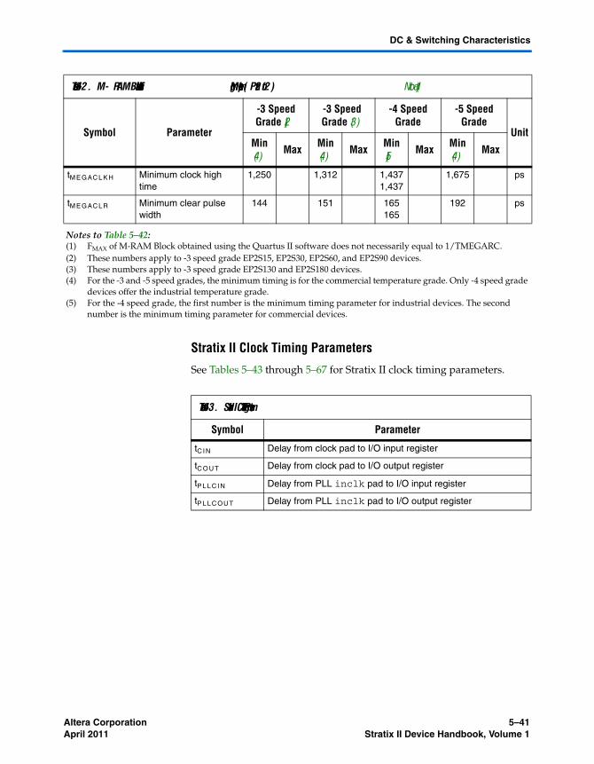
Table 5–42. M-RAM Block Internal Timing Microparameters (Part 1 of 2) Note (1)
Symbol Parameter
-3 Speed Grade (2)
-3 Speed Grade (3)
-4 Speed Grade
-5 Speed Grade
UnitMin (4) Max Min
(4) Max Min (5) Max Min
(4) Max
tM E GA R C Synchronous read cycle time
1,866 2,774 1,866 2,911 1,7771,866
3,189 1,7771,866
3,716 ps
tM E GAW E R E S U Write or read enable setup time before clock
144 151 165165
192 ps
tM E GAW E R E H Write or read enable hold time after clock
39 40 4444
52 ps
tM E GA B E S U Byte enable setup time before clock
50 52 5757
67 ps
tM E GA B E H Byte enable hold time after clock
39 40 4444
52 ps
tM E GA DATA A S U A port data setup time before clock
50 52 5757
67 ps
tM E GA DATA A H A port data hold time after clock
243 255 279279
325 ps
tMEGAADDRASU A port address setup time before clock
589 618 677677
789 ps
tM E GA A DD R A H A port address hold time after clock
241 253 277277
322 ps
tM E GA DATA B S U B port setup time before clock
50 52 5757
67 ps
tM E GA DATA B H B port hold time after clock
243 255 279279
325 ps
tMEGAADDRBSU B port address setup time before clock
589 618 677677
789 ps
tM E GA A DD R B H B port address hold time after clock
241 253 277277
322 ps
tM E GA DATAC O 1 Clock-to-output delay when using output registers
480 715 480 749 457480
821 480 957 ps
tM E GA DATAC O 2 Clock-to-output delay without output registers
1,950 2,899 1,950 3,042 1,8571,950
3,332 1,950 3,884 ps
tM E GAC L K L Minimum clock low time 1,250 1,312 1,4371,437
1,675 ps
Altera Corporation 5–41April 2011 Stratix II Device Handbook, Volume 1
DC & Switching Characteristics
Stratix II Clock Timing Parameters
See Tables 5–43 through 5–67 for Stratix II clock timing parameters.
tM E GAC L K H Minimum clock high time
1,250 1,312 1,4371,437
1,675 ps
tM E GAC L R Minimum clear pulse width
144 151 165165
192 ps
Notes to Table 5–42:(1) FMAX of M-RAM Block obtained using the Quartus II software does not necessarily equal to 1/TMEGARC.(2) These numbers apply to -3 speed grade EP2S15, EP2S30, EP2S60, and EP2S90 devices.(3) These numbers apply to -3 speed grade EP2S130 and EP2S180 devices.(4) For the -3 and -5 speed grades, the minimum timing is for the commercial temperature grade. Only -4 speed grade
devices offer the industrial temperature grade.(5) For the -4 speed grade, the first number is the minimum timing parameter for industrial devices. The second
number is the minimum timing parameter for commercial devices.
Table 5–42. M-RAM Block Internal Timing Microparameters (Part 2 of 2) Note (1)
Symbol Parameter
-3 Speed Grade (2)
-3 Speed Grade (3)
-4 Speed Grade
-5 Speed Grade
UnitMin (4) Max Min
(4) Max Min (5) Max Min
(4) Max
Table 5–43. Stratix II Clock Timing Parameters
Symbol Parameter
tC I N Delay from clock pad to I/O input register
tC O UT Delay from clock pad to I/O output register
tP L L C I N Delay from PLL inclk pad to I/O input register
tP L L C O U T Delay from PLL inclk pad to I/O output register

5–42 Altera CorporationStratix II Device Handbook, Volume 1 April 2011
Timing Model
EP2S15 Clock Timing Parameters
Tables 5–44 though 5–47 show the maximum clock timing parameters for EP2S15 devices.
Table 5–44. EP2S15 Column Pins Regional Clock Timing Parameters
ParameterMinimum Timing -3 Speed
Grade-4 Speed
Grade-5 Speed
Grade UnitIndustrial Commercial
tC I N 1.445 1.512 2.487 2.848 3.309 ns
tC O UT 1.288 1.347 2.245 2.570 2.985 ns
tP L L C I N 0.104 0.102 0.336 0.373 0.424 ns
tP L L C O UT -0.053 -0.063 0.094 0.095 0.1 ns
Table 5–45. EP2S15 Column Pins Global Clock Timing Parameters
ParameterMinimum Timing -3 Speed
Grade-4 Speed
Grade-5 Speed
Grade UnitIndustrial Commercial
tC I N 1.419 1.487 2.456 2.813 3.273 ns
tC O UT 1.262 1.322 2.214 2.535 2.949 ns
tP L L C I N 0.094 0.092 0.326 0.363 0.414 ns
tP L L C O UT -0.063 -0.073 0.084 0.085 0.09 ns
Table 5–46. EP2S15 Row Pins Regional Clock Timing Parameters
ParameterMinimum Timing -3 Speed
Grade-4 Speed
Grade-5 Speed
Grade UnitIndustrial Commercial
tC I N 1.232 1.288 2.144 2.454 2.848 ns
tC O UT 1.237 1.293 2.140 2.450 2.843 ns
tP L L C I N -0.109 -0.122 -0.007 -0.021 -0.037 ns
tP L L C O UT -0.104 -0.117 -0.011 -0.025 -0.042 ns
Altera Corporation 5–43April 2011 Stratix II Device Handbook, Volume 1
DC & Switching Characteristics
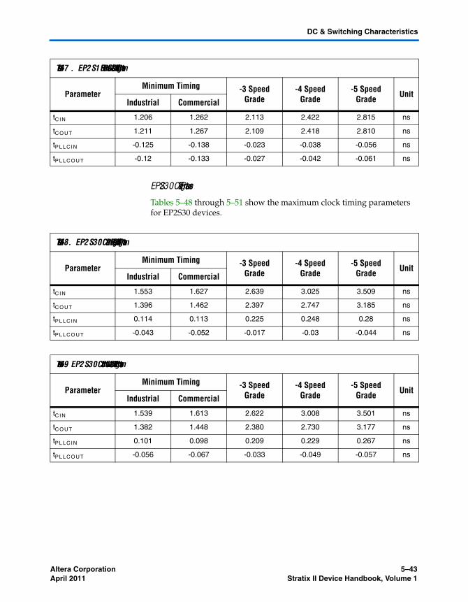
EP2S30 Clock Timing Parameters
Tables 5–48 through 5–51 show the maximum clock timing parameters for EP2S30 devices.
Table 5–47. EP2S15 Row Pins Global Clock Timing Parameters
ParameterMinimum Timing -3 Speed
Grade-4 Speed
Grade-5 Speed
Grade UnitIndustrial Commercial
tC I N 1.206 1.262 2.113 2.422 2.815 ns
tC O UT 1.211 1.267 2.109 2.418 2.810 ns
tP L L C I N -0.125 -0.138 -0.023 -0.038 -0.056 ns
tP L L C O UT -0.12 -0.133 -0.027 -0.042 -0.061 ns
Table 5–48. EP2S30 Column Pins Regional Clock Timing Parameters
ParameterMinimum Timing -3 Speed
Grade-4 Speed
Grade-5 Speed
Grade UnitIndustrial Commercial
tC I N 1.553 1.627 2.639 3.025 3.509 ns
tC O UT 1.396 1.462 2.397 2.747 3.185 ns
tP L L C I N 0.114 0.113 0.225 0.248 0.28 ns
tP L L C O UT -0.043 -0.052 -0.017 -0.03 -0.044 ns
Table 5–49. EP2S30 Column Pins Global Clock Timing Parameters
ParameterMinimum Timing -3 Speed
Grade-4 Speed
Grade-5 Speed
Grade UnitIndustrial Commercial
tC I N 1.539 1.613 2.622 3.008 3.501 ns
tC O UT 1.382 1.448 2.380 2.730 3.177 ns
tP L L C I N 0.101 0.098 0.209 0.229 0.267 ns
tP L L C O UT -0.056 -0.067 -0.033 -0.049 -0.057 ns
5–44 Altera CorporationStratix II Device Handbook, Volume 1 April 2011
Timing Model
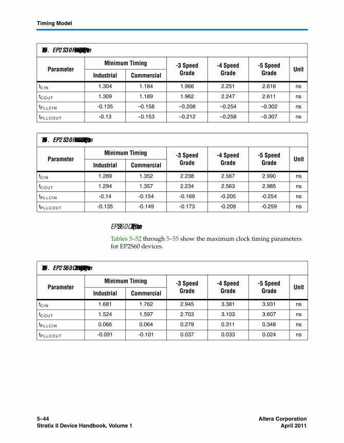
EP2S60 Clock Timing Parameters
Tables 5–52 through 5–55 show the maximum clock timing parameters for EP2S60 devices.
Table 5–50. EP2S30 Row Pins Regional Clock Timing Parameters
ParameterMinimum Timing -3 Speed
Grade-4 Speed
Grade-5 Speed
Grade UnitIndustrial Commercial
tC I N 1.304 1.184 1.966 2.251 2.616 ns
tC O UT 1.309 1.189 1.962 2.247 2.611 ns
tP L L C I N -0.135 –0.158 –0.208 –0.254 –0.302 ns
tP L L C O UT -0.13 –0.153 –0.212 –0.258 –0.307 ns
Table 5–51. EP2S30 Row Pins Global Clock Timing Parameters
ParameterMinimum Timing -3 Speed
Grade-4 Speed
Grade-5 Speed
Grade UnitIndustrial Commercial
tC I N 1.289 1.352 2.238 2.567 2.990 ns
tC O UT 1.294 1.357 2.234 2.563 2.985 ns
tP L L C I N -0.14 -0.154 -0.169 -0.205 -0.254 ns
tP L L C O UT -0.135 -0.149 -0.173 -0.209 -0.259 ns
Table 5–52. EP2S60 Column Pins Regional Clock Timing Parameters
ParameterMinimum Timing -3 Speed
Grade-4 Speed
Grade-5 Speed
Grade UnitIndustrial Commercial
tC I N 1.681 1.762 2.945 3.381 3.931 ns
tC O UT 1.524 1.597 2.703 3.103 3.607 ns
tP L L C I N 0.066 0.064 0.279 0.311 0.348 ns
tP L L C O UT -0.091 -0.101 0.037 0.033 0.024 ns

Altera Corporation 5–45April 2011 Stratix II Device Handbook, Volume 1
DC & Switching Characteristics
Table 5–53. EP2S60 Column Pins Global Clock Timing Parameters
ParameterMinimum Timing -3 Speed
Grade-4 Speed
Grade-5 Speed
Grade UnitIndustrial Commercial
tC I N 1.658 1.739 2.920 3.350 3.899 ns
tC O UT 1.501 1.574 2.678 3.072 3.575 ns
tP L L C I N 0.06 0.057 0.278 0.304 0.355 ns
tP L L C O UT -0.097 -0.108 0.036 0.026 0.031 ns
Table 5–54. EP2S60 Row Pins Regional Clock Timing Parameters
ParameterMinimum Timing -3 Speed
Grade-4 Speed
Grade-5 Speed
Grade UnitIndustrial Commercial
tC I N 1.463 1.532 2.591 2.972 3.453 ns
tC O UT 1.468 1.537 2.587 2.968 3.448 ns
tP L L C I N -0.153 -0.167 -0.079 -0.099 -0.128 ns
tP L L C O UT -0.148 -0.162 -0.083 -0.103 -0.133 ns
Table 5–55. EP2S60 Row Pins Global Clock Timing Parameters
ParameterMinimum Timing -3 Speed
Grade-4 Speed
Grade-5 Speed
Grade UnitIndustrial Commercial
tC I N 1.439 1.508 2.562 2.940 3.421 ns
tC O UT 1.444 1.513 2.558 2.936 3.416 ns
tP L L C I N -0.161 -0.174 -0.083 -0.107 -0.126 ns
tP L L C O UT -0.156 -0.169 -0.087 -0.111 -0.131 ns

5–46 Altera CorporationStratix II Device Handbook, Volume 1 April 2011
Timing Model
EP2S90 Clock Timing Parameters
Tables 5–56 through 5–59 show the maximum clock timing parameters for EP2S90 devices.
Table 5–56. EP2S90 Column Pins Regional Clock Timing Parameters
ParameterMinimum Timing -3 Speed
Grade-4 Speed
Grade-5 Speed
Grade UnitIndustrial Commercial
tC I N 1.768 1.850 3.033 3.473 4.040 ns
tC O UT 1.611 1.685 2.791 3.195 3.716 ns
tP L L C I N -0.127 -0.117 0.125 0.129 0.144 ns
tP L L C O UT -0.284 -0.282 -0.117 -0.149 -0.18 ns
Table 5–57. EP2S90 Column Pins Global Clock Timing Parameters
ParameterMinimum Timing -3 Speed
Grade-4 Speed
Grade-5 Speed
Grade UnitIndustrial Commercial
tC I N 1.783 1.868 3.058 3.502 4.070 ns
tC O UT 1.626 1.703 2.816 3.224 3.746 ns
tP L L C I N -0.137 -0.127 0.115 0.119 0.134 ns
tP L L C O UT -0.294 -0.292 -0.127 -0.159 -0.19 ns
Table 5–58. EP2S90 Row Pins Regional Clock Timing Parameters
ParameterMinimum Timing -3 Speed
Grade-4 Speed
Grade-5 Speed
Grade UnitIndustrial Commercial
tC I N 1.566 1.638 2.731 3.124 3.632 ns
tC O UT 1.571 1.643 2.727 3.120 3.627 ns
tP L L C I N -0.326 -0.326 -0.178 -0.218 -0.264 ns
tP L L C O UT -0.321 -0.321 -0.182 -0.222 -0.269 ns

Altera Corporation 5–47April 2011 Stratix II Device Handbook, Volume 1
DC & Switching Characteristics
EP2S130 Clock Timing Parameters
Tables 5–60 through 5–63 show the maximum clock timing parameters for EP2S130 devices.
Table 5–59. EP2S90 Row Pins Global Clock Timing Parameters
ParameterMinimum Timing -3 Speed
Grade-4 Speed
Grade-5 Speed
Grade UnitIndustrial Commercial
tC I N 1.585 1.658 2.757 3.154 3.665 ns
tC O UT 1.590 1.663 2.753 3.150 3.660 ns
tP L L C I N -0.341 -0.341 -0.193 -0.235 -0.278 ns
tP L L C O UT -0.336 -0.336 -0.197 -0.239 -0.283 ns
Table 5–60. EP2S130 Column Pins Regional Clock Timing Parameters
ParameterMinimum Timing -3 Speed
Grade-4 Speed
Grade-5 Speed
Grade UnitIndustrial Commercial
tC I N 1.889 1.981 3.405 3.722 4.326 ns
tC O UT 1.732 1.816 3.151 3.444 4.002 ns
tP L L C I N 0.105 0.106 0.226 0.242 0.277 ns
tP L L C O UT -0.052 -0.059 -0.028 -0.036 -0.047 ns
Table 5–61. EP2S130 Column Pins Global Clock Timing Parameters
ParameterMinimum Timing -3 Speed
Grade-4 Speed
Grade-5 Speed
Grade UnitIndustrial Commercial
tC I N 1.907 1.998 3.420 3.740 4.348 ns
tC O UT 1.750 1.833 3.166 3.462 4.024 ns
tP L L C I N 0.134 0.136 0.276 0.296 0.338 ns
tP L L C O UT -0.023 -0.029 0.022 0.018 0.014 ns
5–48 Altera CorporationStratix II Device Handbook, Volume 1 April 2011
Timing Model
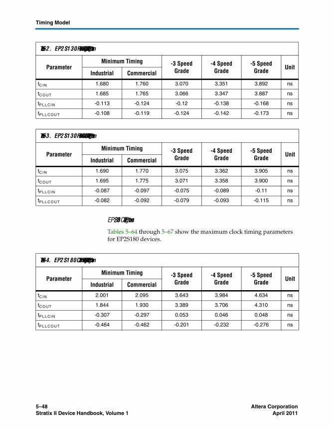
EP2S180 Clock Timing Parameters
Tables 5–64 through 5–67 show the maximum clock timing parameters for EP2S180 devices.
Table 5–62. EP2S130 Row Pins Regional Clock Timing Parameters
ParameterMinimum Timing -3 Speed
Grade-4 Speed
Grade-5 Speed
Grade UnitIndustrial Commercial
tC I N 1.680 1.760 3.070 3.351 3.892 ns
tC O UT 1.685 1.765 3.066 3.347 3.887 ns
tP L L C I N -0.113 -0.124 -0.12 -0.138 -0.168 ns
tP L L C O UT -0.108 -0.119 -0.124 -0.142 -0.173 ns
Table 5–63. EP2S130 Row Pins Global Clock Timing Parameters
ParameterMinimum Timing -3 Speed
Grade-4 Speed
Grade-5 Speed
Grade UnitIndustrial Commercial
tC I N 1.690 1.770 3.075 3.362 3.905 ns
tC O UT 1.695 1.775 3.071 3.358 3.900 ns
tP L L C I N -0.087 -0.097 -0.075 -0.089 -0.11 ns
tP L L C O UT -0.082 -0.092 -0.079 -0.093 -0.115 ns
Table 5–64. EP2S180 Column Pins Regional Clock Timing Parameters
ParameterMinimum Timing -3 Speed
Grade-4 Speed
Grade-5 Speed
Grade UnitIndustrial Commercial
tC I N 2.001 2.095 3.643 3.984 4.634 ns
tC O UT 1.844 1.930 3.389 3.706 4.310 ns
tP L L C I N -0.307 -0.297 0.053 0.046 0.048 ns
tP L L C O UT -0.464 -0.462 -0.201 -0.232 -0.276 ns
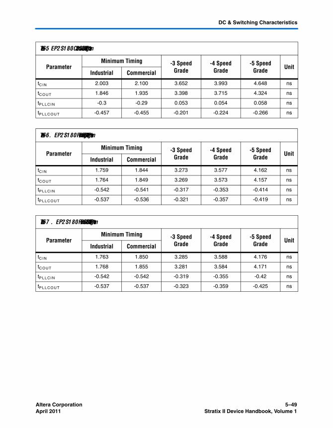
Altera Corporation 5–49April 2011 Stratix II Device Handbook, Volume 1
DC & Switching Characteristics
Table 5–65. EP2S180 Column Pins Global Clock Timing Parameters
ParameterMinimum Timing -3 Speed
Grade-4 Speed
Grade-5 Speed
Grade UnitIndustrial Commercial
tC I N 2.003 2.100 3.652 3.993 4.648 ns
tC O UT 1.846 1.935 3.398 3.715 4.324 ns
tP L L C I N -0.3 -0.29 0.053 0.054 0.058 ns
tP L L C O UT -0.457 -0.455 -0.201 -0.224 -0.266 ns
Table 5–66. EP2S180 Row Pins Regional Clock Timing Parameters
ParameterMinimum Timing -3 Speed
Grade-4 Speed
Grade-5 Speed
Grade UnitIndustrial Commercial
tC I N 1.759 1.844 3.273 3.577 4.162 ns
tC O UT 1.764 1.849 3.269 3.573 4.157 ns
tP L L C I N -0.542 -0.541 -0.317 -0.353 -0.414 ns
tP L L C O UT -0.537 -0.536 -0.321 -0.357 -0.419 ns
Table 5–67. EP2S180 Row Pins Global Clock Timing Parameters
ParameterMinimum Timing -3 Speed
Grade-4 Speed
Grade-5 Speed
Grade UnitIndustrial Commercial
tC I N 1.763 1.850 3.285 3.588 4.176 ns
tC O UT 1.768 1.855 3.281 3.584 4.171 ns
tP L L C I N -0.542 -0.542 -0.319 -0.355 -0.42 ns
tP L L C O UT -0.537 -0.537 -0.323 -0.359 -0.425 ns

5–50 Altera CorporationStratix II Device Handbook, Volume 1 April 2011
Timing Model
Clock Network Skew Adders
The Quartus II software models skew within dedicated clock networks such as global and regional clocks. Therefore, intra-clock network skew adder is not specified. Table 5–68 specifies the clock skew between any two clock networks driving registers in the IOE.
Table 5–68. Clock Network Specifications
Name Description Min Typ Max Unit
Clock skew adderEP2S15, EP2S30, EP2S60 (1)
Inter-clock network, same side ±50 ps
Inter-clock network, entire chip ±100 ps
Clock skew adderEP2S90 (1)
Inter-clock network, same side ±55 ps
Inter-clock network, entire chip ±110 ps
Clock skew adderEP2S130 (1)
Inter-clock network, same side ±63 ps
Inter-clock network, entire chip ±125 ps
Clock skew adderEP2S180 (1)
Inter-clock network, same side ±75 ps
Inter-clock network, entire chip ±150 ps
Note to Table 5–68:(1) This is in addition to intra-clock network skew, which is modeled in the Quartus II software.

Altera Corporation 5–51April 2011 Stratix II Device Handbook, Volume 1
DC & Switching Characteristics
IOE Programmable Delay
See Tables 5–69 and 5–70 for IOE programmable delay.
Table 5–69. Stratix II IOE Programmable Delay on Column Pins Note (1)
Parameter Paths Affected Available Settings
Minimum Timing (2)
-3 Speed Grade (3)
-4 Speed Grade
-5 Speed Grade
Min Offset (ps)
Max Offset (ps)
Min Offset (ps)
Max Offset (ps)
Min Offset (ps)
Max Offset (ps)
Min Offset (ps)
Max Offset (ps)
Input delay from pin to internal cells
Pad to I/O dataout to logic array
8 00
1,6961,781
00
2,8813,025
0 3,313 0 3,860
Input delay from pin to input register
Pad to I/O input register
64 00
1,9552,053
00
3,2753,439
0 3,766 0 4,388
Delay from output register to output pin
I/O output register to pad
2 00
316332
00
500525
0 575 0 670
Output enable pin delay
tX Z, tZ X 2 00
305320
00
483507
0 556 0 647
Notes to Table 5–69:(1) The incremental values for the settings are generally linear. For the exact delay associated with each setting, use the
latest version of the Quartus II software.(2) The first number is the minimum timing parameter for industrial devices. The second number is the minimum
timing parameter for commercial devices.(3) The first number applies to -3 speed grade EP2S15, EP2S30, EP2S60, and EP2S90 devices. The second number
applies to -3 speed grade EP2S130 and EP2S180 devices.

5–52 Altera CorporationStratix II Device Handbook, Volume 1 April 2011
Timing Model
Default Capacitive Loading of Different I/O Standards
See Table 5–71 for default capacitive loading of different I/O standards.
Table 5–70. Stratix II IOE Programmable Delay on Row Pins Note (1)
Parameter Paths Affected Available Settings
Minimum Timing (2)
-3 Speed Grade (3)
-4 Speed Grade
-5 Speed Grade
Min Offset (ps)
Max Offset (ps)
Min Offset (ps)
Max Offset (ps)
Min Offset (ps)
Max Offset (ps)
Min Offset (ps)
Max Offset (ps)
Input delay from pin to internal cells
Pad to I/O dataout to logic array
8 00
1,6971,782
00
2,8763,020
0 3,308 0 3,853
Input delay from pin to input register
Pad to I/O input register
64 00
1,9562,054
00
3,2703,434
0 3,761 0 4,381
Delay from output register to output pin
I/O output register to pad
2 00
316332
00
525525
0 575 0 670
Output enable pin delay
tX Z , tZ X 2 00
305320
00
507507
0 556 0 647
Notes to Table 5–70:(1) The incremental values for the settings are generally linear. For the exact delay associated with each setting, use the
latest version of the Quartus II software.(2) The first number is the minimum timing parameter for industrial devices. The second number is the minimum
timing parameter for commercial devices.(3) The first number applies to -3 speed grade EP2S15, EP2S30, EP2S60, and EP2S90 devices. The second number
applies to -3 speed grade EP2S130 and EP2S180 devices.
Table 5–71. Default Loading of Different I/O Standards for Stratix II (Part 1 of 2)
I/O Standard Capacitive Load Unit
LVTTL 0 pF
LVCMOS 0 pF
2.5 V 0 pF
1.8 V 0 pF
1.5 V 0 pF
PCI 10 pF
PCI-X 10 pF
SSTL-2 Class I 0 pF

Altera Corporation 5–53April 2011 Stratix II Device Handbook, Volume 1
DC & Switching Characteristics
SSTL-2 Class II 0 pF
SSTL-18 Class I 0 pF
SSTL-18 Class II 0 pF
1.5-V HSTL Class I 0 pF
1.5-V HSTL Class II 0 pF
1.8-V HSTL Class I 0 pF
1.8-V HSTL Class II 0 pF
1.2-V HSTL with OCT 0 pF
Differential SSTL-2 Class I 0 pF
Differential SSTL-2 Class II 0 pF
Differential SSTL-18 Class I 0 pF
Differential SSTL-18 Class II 0 pF
1.5-V Differential HSTL Class I 0 pF
1.5-V Differential HSTL Class II 0 pF
1.8-V Differential HSTL Class I 0 pF
1.8-V Differential HSTL Class II 0 pF
LVDS 0 pF
HyperTransport 0 pF
LVPECL 0 pF
Table 5–71. Default Loading of Different I/O Standards for Stratix II (Part 2 of 2)
I/O Standard Capacitive Load Unit

5–54 Altera CorporationStratix II Device Handbook, Volume 1 April 2011
Timing Model
I/O Delays
See Tables 5–72 through 5–76 for I/O delays.
Table 5–72. I/O Delay Parameters
Symbol Parameter
tD I P Delay from I/O datain to output pad
tO P Delay from I/O output register to output pad
tP CO U T Delay from input pad to I/O dataout to core
tP I Delay from input pad to I/O input register
Table 5–73. Stratix II I/O Input Delay for Column Pins (Part 1 of 3)
I/O Standard ParameterMinimum Timing -3 Speed
Grade (2)
-3 Speed Grade
(3)
-4 Speed Grade
-5 Speed Grade Unit
Industrial Commercial
LVTTL tP I 674 707 1223 1282 1405 1637 ps
tP C O U T 408 428 787 825 904 1054 ps
2.5 V tP I 684 717 1210 1269 1390 1619 ps
tP C O U T 418 438 774 812 889 1036 ps
1.8 V tP I 747 783 1366 1433 1570 1829 ps
tP C O U T 481 504 930 976 1069 1246 ps
1.5 V tP I 749 786 1436 1506 1650 1922 ps
tP C O U T 483 507 1000 1049 1149 1339 ps
LVCMOS tP I 674 707 1223 1282 1405 1637 ps
tP C O U T 408 428 787 825 904 1054 ps
SSTL-2 Class I tP I 507 530 818 857 939 1094 ps
tP C O U T 241 251 382 400 438 511 ps
SSTL-2 Class II tP I 507 530 818 857 939 1094 ps
tP C O U T 241 251 382 400 438 511 ps
SSTL-18 Class I tP I 543 569 898 941 1031 1201 ps
tP C O U T 277 290 462 484 530 618 ps
SSTL-18 Class II tP I 543 569 898 941 1031 1201 ps
tP C O U T 277 290 462 484 530 618 ps
1.5-V HSTL Class I
tP I 560 587 993 1041 1141 1329 ps
tP C O U T 294 308 557 584 640 746 ps

Altera Corporation 5–55April 2011 Stratix II Device Handbook, Volume 1
DC & Switching Characteristics
1.5-V HSTL Class II
tP I 560 587 993 1041 1141 1329 ps
tP C O U T 294 308 557 584 640 746 ps
1.8-V HSTL Class I
tP I 543 569 898 941 1031 1201 ps
tP C O U T 277 290 462 484 530 618 ps
1.8-V HSTL Class II
tP I 543 569 898 941 1031 1201 ps
tP C O U T 277 290 462 484 530 618 ps
PCI tP I 679 712 1214 1273 1395 1625 ps
tP C O U T 413 433 778 816 894 1042 ps
PCI-X tP I 679 712 1214 1273 1395 1625 ps
tP C O U T 413 433 778 816 894 1042 ps
Differential SSTL-2 Class I (1)
tP I 507 530 818 857 939 1094 ps
tP C O U T 241 251 382 400 438 511 ps
Differential SSTL-2 Class II (1)
tP I 507 530 818 857 939 1094 ps
tP C O U T 241 251 382 400 438 511 ps
Differential SSTL-18 Class I (1)
tP I 543 569 898 941 1031 1201 ps
tP C O U T 277 290 462 484 530 618 ps
Differential SSTL-18 Class II (1)
tP I 543 569 898 941 1031 1201 ps
tP C O U T 277 290 462 484 530 618 ps
1.8-V Differential HSTL Class I (1)
tP I 543 569 898 941 1031 1201 ps
tP C O U T 277 290 462 484 530 618 ps
1.8-V Differential HSTL Class II (1)
tP I 543 569 898 941 1031 1201 ps
tP C O U T 277 290 462 484 530 618 ps
1.5-V Differential HSTL Class I (1)
tP I 560 587 993 1041 1141 1329 ps
tP C O U T 294 308 557 584 640 746 ps
1.5-V Differential HSTL Class II (1)
tP I 560 587 993 1041 1141 1329 ps
tP C O U T 294 308 557 584 640 746 ps
Table 5–73. Stratix II I/O Input Delay for Column Pins (Part 2 of 3)
I/O Standard ParameterMinimum Timing -3 Speed
Grade (2)
-3 Speed Grade
(3)
-4 Speed Grade
-5 Speed Grade Unit
Industrial Commercial
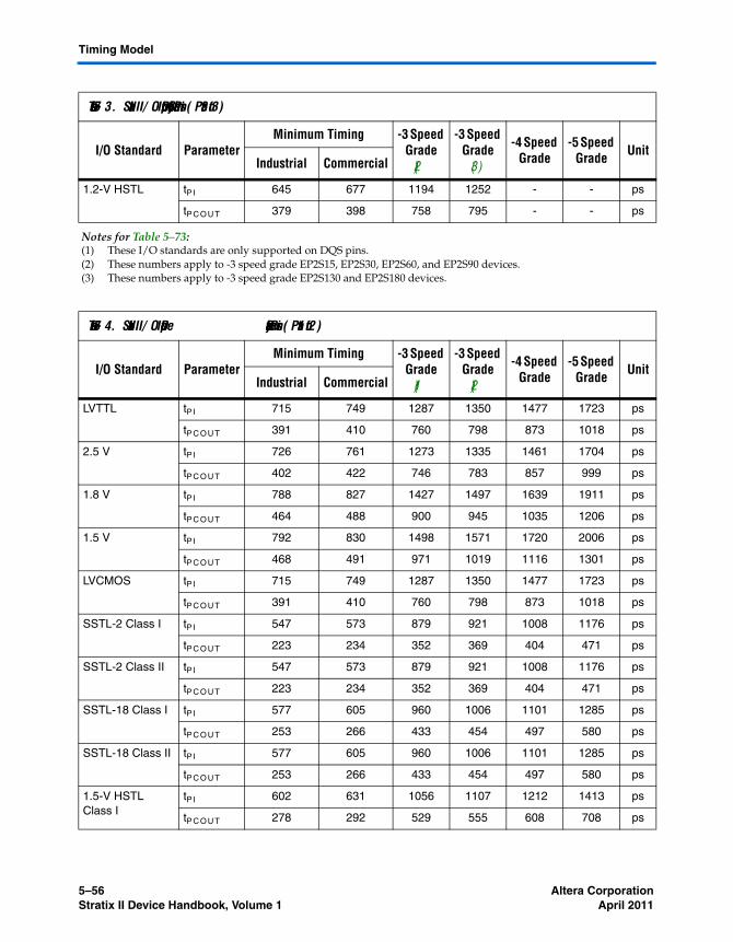
5–56 Altera CorporationStratix II Device Handbook, Volume 1 April 2011
Timing Model
1.2-V HSTL tP I 645 677 1194 1252 - - ps
tP C O U T 379 398 758 795 - - ps
Notes for Table 5–73:(1) These I/O standards are only supported on DQS pins.(2) These numbers apply to -3 speed grade EP2S15, EP2S30, EP2S60, and EP2S90 devices.(3) These numbers apply to -3 speed grade EP2S130 and EP2S180 devices.
Table 5–74. Stratix II I/O Input Delay for Row Pins (Part 1 of 2)
I/O Standard Parameter Minimum Timing -3 Speed
Grade (1)
-3 Speed Grade
(2)
-4 Speed Grade
-5 Speed Grade Unit
Industrial Commercial
LVTTL tP I 715 749 1287 1350 1477 1723 ps
tP C O U T 391 410 760 798 873 1018 ps
2.5 V tP I 726 761 1273 1335 1461 1704 ps
tP C O U T 402 422 746 783 857 999 ps
1.8 V tP I 788 827 1427 1497 1639 1911 ps
tP C O U T 464 488 900 945 1035 1206 ps
1.5 V tP I 792 830 1498 1571 1720 2006 ps
tP C O U T 468 491 971 1019 1116 1301 ps
LVCMOS tP I 715 749 1287 1350 1477 1723 ps
tP C O U T 391 410 760 798 873 1018 ps
SSTL-2 Class I tP I 547 573 879 921 1008 1176 ps
tP C O U T 223 234 352 369 404 471 ps
SSTL-2 Class II tP I 547 573 879 921 1008 1176 ps
tP C O U T 223 234 352 369 404 471 ps
SSTL-18 Class I tP I 577 605 960 1006 1101 1285 ps
tP C O U T 253 266 433 454 497 580 ps
SSTL-18 Class II tP I 577 605 960 1006 1101 1285 ps
tP C O U T 253 266 433 454 497 580 ps
1.5-V HSTL Class I
tP I 602 631 1056 1107 1212 1413 ps
tP C O U T 278 292 529 555 608 708 ps
Table 5–73. Stratix II I/O Input Delay for Column Pins (Part 3 of 3)
I/O Standard ParameterMinimum Timing -3 Speed
Grade (2)
-3 Speed Grade
(3)
-4 Speed Grade
-5 Speed Grade Unit
Industrial Commercial

Altera Corporation 5–57April 2011 Stratix II Device Handbook, Volume 1
DC & Switching Characteristics
1.5-V HSTL Class II
tP I 602 631 1056 1107 1212 1413 ps
tP C O U T 278 292 529 555 608 708 ps
1.8-V HSTL Class I
tP I 577 605 960 1006 1101 1285 ps
tP C O U T 253 266 433 454 497 580 ps
1.8-V HSTL Class II
tP I 577 605 960 1006 1101 1285 ps
tP C O U T 253 266 433 454 497 580 ps
LVDS tP I 515 540 948 994 1088 1269 ps
tP C O U T 191 201 421 442 484 564 ps
HyperTransport tP I 515 540 948 994 1088 1269 ps
tP C O U T 191 201 421 442 484 564 ps
Notes for Table 5–74:(1) These numbers apply to -3 speed grade EP2S15, EP2S30, EP2S60, and EP2S90 devices.(2) These numbers apply to -3 speed grade EP2S130 and EP2S180 devices.
Table 5–75. Stratix II I/O Output Delay for Column Pins (Part 1 of 8)
I/O Standard Drive Strength Parameter
Minimum Timing -3 Speed Grade
(3)
-3 Speed Grade
(4)
-4 Speed Grade
-5 Speed Grade
Unit Industrial Commercial
LVTTL 4 mA tO P 1178 1236 2351 2467 2702 2820 ps
tD I P 1198 1258 2417 2537 2778 2910 ps
8 mA tO P 1041 1091 2036 2136 2340 2448 ps
tD I P 1061 1113 2102 2206 2416 2538 ps
12 mA tO P 976 1024 2036 2136 2340 2448 ps
tD I P 996 1046 2102 2206 2416 2538 ps
16 mA tO P 951 998 1893 1986 2176 2279 ps
tD I P 971 1020 1959 2056 2252 2369 ps
20 mA tO P 931 976 1787 1875 2054 2154 ps
tD I P 951 998 1853 1945 2130 2244 ps
24 mA (1)
tO P 924 969 1788 1876 2055 2156 ps
tD I P 944 991 1854 1946 2131 2246 ps
Table 5–74. Stratix II I/O Input Delay for Row Pins (Part 2 of 2)
I/O Standard Parameter Minimum Timing -3 Speed
Grade (1)
-3 Speed Grade
(2)
-4 Speed Grade
-5 Speed Grade Unit
Industrial Commercial

5–58 Altera CorporationStratix II Device Handbook, Volume 1 April 2011
Timing Model
LVCMOS 4 mA tO P 1041 1091 2036 2136 2340 2448 ps
tD I P 1061 1113 2102 2206 2416 2538 ps
8 mA tO P 952 999 1786 1874 2053 2153 ps
tD I P 972 1021 1852 1944 2129 2243 ps
12 mA tO P 926 971 1720 1805 1977 2075 ps
tD I P 946 993 1786 1875 2053 2165 ps
16 mA tO P 933 978 1693 1776 1946 2043 ps
tD I P 953 1000 1759 1846 2022 2133 ps
20 mA tO P 921 965 1677 1759 1927 2025 ps
tD I P 941 987 1743 1829 2003 2115 ps
24 mA (1)
tO P 909 954 1659 1741 1906 2003 ps
tD I P 929 976 1725 1811 1982 2093 ps
2.5 V 4 mA tO P 1004 1053 2063 2165 2371 2480 ps
tD I P 1024 1075 2129 2235 2447 2570 ps
8 mA tO P 955 1001 1841 1932 2116 2218 ps
tD I P 975 1023 1907 2002 2192 2308 ps
12 mA tO P 934 980 1742 1828 2002 2101 ps
tD I P 954 1002 1808 1898 2078 2191 ps
16 mA (1)
tO P 918 962 1679 1762 1929 2027 ps
tD I P 938 984 1745 1832 2005 2117 ps
Table 5–75. Stratix II I/O Output Delay for Column Pins (Part 2 of 8)
I/O Standard Drive Strength Parameter
Minimum Timing -3 Speed Grade
(3)
-3 Speed Grade
(4)
-4 Speed Grade
-5 Speed Grade
Unit Industrial Commercial

Altera Corporation 5–59April 2011 Stratix II Device Handbook, Volume 1
DC & Switching Characteristics
1.8 V 2 mA tO P 1042 1093 2904 3048 3338 3472 ps
tD I P 1062 1115 2970 3118 3414 3562 ps
4 mA tO P 1047 1098 2248 2359 2584 2698 ps
tD I P 1067 1120 2314 2429 2660 2788 ps
6 mA tO P 974 1022 2024 2124 2326 2434 ps
tD I P 994 1044 2090 2194 2402 2524 ps
8 mA tO P 976 1024 1947 2043 2238 2343 ps
tD I P 996 1046 2013 2113 2314 2433 ps
10 mA tO P 933 978 1882 1975 2163 2266 ps
tD I P 953 1000 1948 2045 2239 2356 ps
12 mA (1)
tO P 934 979 1833 1923 2107 2209 ps
tD I P 954 1001 1899 1993 2183 2299 ps
1.5 V 2 mA tO P 1023 1073 2505 2629 2879 3002 ps
tD I P 1043 1095 2571 2699 2955 3092 ps
4 mA tO P 963 1009 2023 2123 2325 2433 ps
tD I P 983 1031 2089 2193 2401 2523 ps
6 mA tO P 966 1012 1923 2018 2210 2315 ps
tD I P 986 1034 1989 2088 2286 2405 ps
8 mA (1) tO P 926 971 1878 1970 2158 2262 ps
tD I P 946 993 1944 2040 2234 2352 ps
SSTL-2 Class I 8 mA tO P 913 957 1715 1799 1971 2041 ps
tD I P 933 979 1781 1869 2047 2131 ps
12 mA (1)
tO P 896 940 1672 1754 1921 1991 ps
tD I P 916 962 1738 1824 1997 2081 ps
SSTL-2 Class II 16 mA tO P 876 918 1609 1688 1849 1918 ps
tD I P 896 940 1675 1758 1925 2008 ps
20 mA tO P 877 919 1598 1676 1836 1905 ps
tD I P 897 941 1664 1746 1912 1995 ps
24 mA (1)
tO P 872 915 1596 1674 1834 1903 ps
tD I P 892 937 1662 1744 1910 1993 ps
Table 5–75. Stratix II I/O Output Delay for Column Pins (Part 3 of 8)
I/O Standard Drive Strength Parameter
Minimum Timing -3 Speed Grade
(3)
-3 Speed Grade
(4)
-4 Speed Grade
-5 Speed Grade
Unit Industrial Commercial

5–60 Altera CorporationStratix II Device Handbook, Volume 1 April 2011
Timing Model
SSTL-18 Class I
4 mA tO P 909 953 1690 1773 1942 2012 ps
tD I P 929 975 1756 1843 2018 2102 ps
6 mA tO P 914 958 1656 1737 1903 1973 ps
tD I P 934 980 1722 1807 1979 2063 ps
8 mA tO P 894 937 1640 1721 1885 1954 ps
tD I P 914 959 1706 1791 1961 2044 ps
10 mA tO P 898 942 1638 1718 1882 1952 ps
tD I P 918 964 1704 1788 1958 2042 ps
12 mA (1)
tO P 891 936 1626 1706 1869 1938 ps
tD I P 911 958 1692 1776 1945 2028 ps
SSTL-18 Class II
8 mA tO P 883 925 1597 1675 1835 1904 ps
tD I P 903 947 1663 1745 1911 1994 ps
16 mA tO P 894 937 1578 1655 1813 1882 ps
tD I P 914 959 1644 1725 1889 1972 ps
18 mA tO P 890 933 1585 1663 1821 1890 ps
tD I P 910 955 1651 1733 1897 1980 ps
20 mA (1)
tO P 890 933 1583 1661 1819 1888 ps
tD I P 910 955 1649 1731 1895 1978 ps
1.8-V HSTL Class I
4 mA tO P 912 956 1608 1687 1848 1943 ps
tD I P 932 978 1674 1757 1924 2033 ps
6 mA tO P 917 962 1595 1673 1833 1928 ps
tD I P 937 984 1661 1743 1909 2018 ps
8 mA tO P 896 940 1586 1664 1823 1917 ps
tD I P 916 962 1652 1734 1899 2007 ps
10 mA tO P 900 944 1591 1669 1828 1923 ps
tD I P 920 966 1657 1739 1904 2013 ps
12 mA (1)
tO P 892 936 1585 1663 1821 1916 ps
tD I P 912 958 1651 1733 1897 2006 ps
Table 5–75. Stratix II I/O Output Delay for Column Pins (Part 4 of 8)
I/O Standard Drive Strength Parameter
Minimum Timing -3 Speed Grade
(3)
-3 Speed Grade
(4)
-4 Speed Grade
-5 Speed Grade
Unit Industrial Commercial
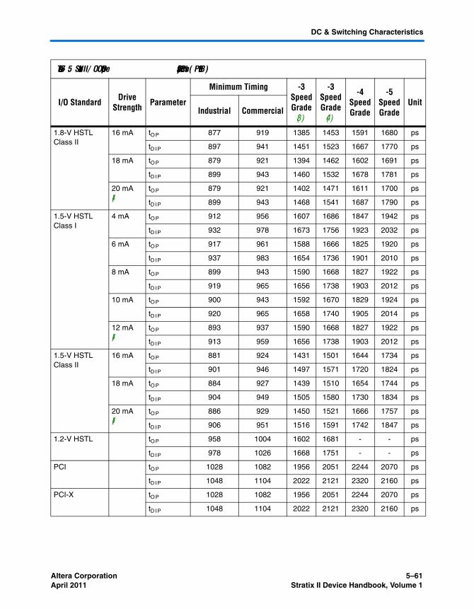
Altera Corporation 5–61April 2011 Stratix II Device Handbook, Volume 1
DC & Switching Characteristics
1.8-V HSTL Class II
16 mA tO P 877 919 1385 1453 1591 1680 ps
tD I P 897 941 1451 1523 1667 1770 ps
18 mA tO P 879 921 1394 1462 1602 1691 ps
tD I P 899 943 1460 1532 1678 1781 ps
20 mA (1)
tO P 879 921 1402 1471 1611 1700 ps
tD I P 899 943 1468 1541 1687 1790 ps
1.5-V HSTL Class I
4 mA tO P 912 956 1607 1686 1847 1942 ps
tD I P 932 978 1673 1756 1923 2032 ps
6 mA tO P 917 961 1588 1666 1825 1920 ps
tD I P 937 983 1654 1736 1901 2010 ps
8 mA tO P 899 943 1590 1668 1827 1922 ps
tD I P 919 965 1656 1738 1903 2012 ps
10 mA tO P 900 943 1592 1670 1829 1924 ps
tD I P 920 965 1658 1740 1905 2014 ps
12 mA (1)
tO P 893 937 1590 1668 1827 1922 ps
tD I P 913 959 1656 1738 1903 2012 ps
1.5-V HSTL Class II
16 mA tO P 881 924 1431 1501 1644 1734 ps
tD I P 901 946 1497 1571 1720 1824 ps
18 mA tO P 884 927 1439 1510 1654 1744 ps
tD I P 904 949 1505 1580 1730 1834 ps
20 mA (1)
tO P 886 929 1450 1521 1666 1757 ps
tD I P 906 951 1516 1591 1742 1847 ps
1.2-V HSTL tO P 958 1004 1602 1681 - - ps
tD I P 978 1026 1668 1751 - - ps
PCI tO P 1028 1082 1956 2051 2244 2070 ps
tD I P 1048 1104 2022 2121 2320 2160 ps
PCI-X tO P 1028 1082 1956 2051 2244 2070 ps
tD I P 1048 1104 2022 2121 2320 2160 ps
Table 5–75. Stratix II I/O Output Delay for Column Pins (Part 5 of 8)
I/O Standard Drive Strength Parameter
Minimum Timing -3 Speed Grade
(3)
-3 Speed Grade
(4)
-4 Speed Grade
-5 Speed Grade
Unit Industrial Commercial

5–62 Altera CorporationStratix II Device Handbook, Volume 1 April 2011
Timing Model
Differential SSTL-2 Class I
8 mA tO P 913 957 1715 1799 1971 2041 ps
tD I P 933 979 1781 1869 2047 2131 ps
12 mA tO P 896 940 1672 1754 1921 1991 ps
tD I P 916 962 1738 1824 1997 2081 ps
Differential SSTL-2 Class II
16 mA tO P 876 918 1609 1688 1849 1918 ps
tD I P 896 940 1675 1758 1925 2008 ps
20 mA tO P 877 919 1598 1676 1836 1905 ps
tD I P 897 941 1664 1746 1912 1995 ps
24 mA tO P 872 915 1596 1674 1834 1903 ps
tD I P 892 937 1662 1744 1910 1993 ps
Differential SSTL-18 Class I
4 mA tO P 909 953 1690 1773 1942 2012 ps
tD I P 929 975 1756 1843 2018 2102 ps
6 mA tO P 914 958 1656 1737 1903 1973 ps
tD I P 934 980 1722 1807 1979 2063 ps
8 mA tO P 894 937 1640 1721 1885 1954 ps
tD I P 914 959 1706 1791 1961 2044 ps
10 mA tO P 898 942 1638 1718 1882 1952 ps
tD I P 918 964 1704 1788 1958 2042 ps
12 mA tO P 891 936 1626 1706 1869 1938 ps
tD I P 911 958 1692 1776 1945 2028 ps
Differential SSTL-18 Class II
8 mA tO P 883 925 1597 1675 1835 1904 ps
tD I P 903 947 1663 1745 1911 1994 ps
16 mA tO P 894 937 1578 1655 1813 1882 ps
tD I P 914 959 1644 1725 1889 1972 ps
18 mA tO P 890 933 1585 1663 1821 1890 ps
tD I P 910 955 1651 1733 1897 1980 ps
20 mA tO P 890 933 1583 1661 1819 1888 ps
tD I P 910 955 1649 1731 1895 1978 ps
Table 5–75. Stratix II I/O Output Delay for Column Pins (Part 6 of 8)
I/O Standard Drive Strength Parameter
Minimum Timing -3 Speed Grade
(3)
-3 Speed Grade
(4)
-4 Speed Grade
-5 Speed Grade
Unit Industrial Commercial

Altera Corporation 5–63April 2011 Stratix II Device Handbook, Volume 1
DC & Switching Characteristics
1.8-V Differential HSTL Class I
4 mA tO P 912 956 1608 1687 1848 1943 ps
tD I P 932 978 1674 1757 1924 2033 ps
6 mA tO P 917 962 1595 1673 1833 1928 ps
tD I P 937 984 1661 1743 1909 2018 ps
8 mA tO P 896 940 1586 1664 1823 1917 ps
tD I P 916 962 1652 1734 1899 2007 ps
10 mA tO P 900 944 1591 1669 1828 1923 ps
tD I P 920 966 1657 1739 1904 2013 ps
12 mA tO P 892 936 1585 1663 1821 1916 ps
tD I P 912 958 1651 1733 1897 2006 ps
1.8-V Differential HSTL Class II
16 mA tO P 877 919 1385 1453 1591 1680 ps
tD I P 897 941 1451 1523 1667 1770 ps
18 mA tO P 879 921 1394 1462 1602 1691 ps
tD I P 899 943 1460 1532 1678 1781 ps
20 mA tO P 879 921 1402 1471 1611 1700 ps
tD I P 899 943 1468 1541 1687 1790 ps
1.5-V Differential HSTL Class I
4 mA tO P 912 956 1607 1686 1847 1942 ps
tD I P 932 978 1673 1756 1923 2032 ps
6 mA tO P 917 961 1588 1666 1825 1920 ps
tD I P 937 983 1654 1736 1901 2010 ps
8 mA tO P 899 943 1590 1668 1827 1922 ps
tD I P 919 965 1656 1738 1903 2012 ps
10 mA tO P 900 943 1592 1670 1829 1924 ps
tD I P 920 965 1658 1740 1905 2014 ps
12 mA tO P 893 937 1590 1668 1827 1922
tD I P 913 959 1656 1738 1903 2012
Table 5–75. Stratix II I/O Output Delay for Column Pins (Part 7 of 8)
I/O Standard Drive Strength Parameter
Minimum Timing -3 Speed Grade
(3)
-3 Speed Grade
(4)
-4 Speed Grade
-5 Speed Grade
Unit Industrial Commercial
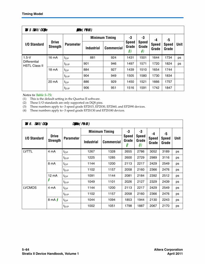
5–64 Altera CorporationStratix II Device Handbook, Volume 1 April 2011
Timing Model
1.5-V Differential HSTL Class II
16 mA tO P 881 924 1431 1501 1644 1734 ps
tD I P 901 946 1497 1571 1720 1824 ps
18 mA tO P 884 927 1439 1510 1654 1744
tD I P 904 949 1505 1580 1730 1834
20 mA tO P 886 929 1450 1521 1666 1757
tD I P 906 951 1516 1591 1742 1847
Notes to Table 5–75:(1) This is the default setting in the Quartus II software.(2) These I/O standards are only supported on DQS pins.(3) These numbers apply to -3 speed grade EP2S15, EP2S30, EP2S60, and EP2S90 devices.(4) These numbers apply to -3 speed grade EP2S130 and EP2S180 devices.
Table 5–76. Stratix II I/O Output Delay for Row Pins (Part 1 of 3)
I/O Standard Drive Strength Parameter
Minimum Timing -3 Speed Grade
(2)
-3 Speed Grade
(3)
-4 Speed Grade
-5 Speed Grade
Unit Industrial Commercial
LVTTL 4 mA tO P 1267 1328 2655 2786 3052 3189 ps
tD I P 1225 1285 2600 2729 2989 3116 ps
8 mA tO P 1144 1200 2113 2217 2429 2549 ps
tD I P 1102 1157 2058 2160 2366 2476 ps
12 mA (1)
tO P 1091 1144 2081 2184 2392 2512 ps
tD I P 1049 1101 2026 2127 2329 2439 ps
LVCMOS 4 mA tO P 1144 1200 2113 2217 2429 2549 ps
tD I P 1102 1157 2058 2160 2366 2476 ps
8 mA (1) tO P 1044 1094 1853 1944 2130 2243 ps
tD I P 1002 1051 1798 1887 2067 2170 ps
Table 5–75. Stratix II I/O Output Delay for Column Pins (Part 8 of 8)
I/O Standard Drive Strength Parameter
Minimum Timing -3 Speed Grade
(3)
-3 Speed Grade
(4)
-4 Speed Grade
-5 Speed Grade
Unit Industrial Commercial
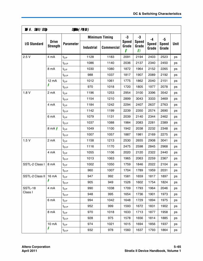
Altera Corporation 5–65April 2011 Stratix II Device Handbook, Volume 1
DC & Switching Characteristics
2.5 V 4 mA tO P 1128 1183 2091 2194 2403 2523 ps
tD I P 1086 1140 2036 2137 2340 2450 ps
8 mA tO P 1030 1080 1872 1964 2152 2265 ps
tD I P 988 1037 1817 1907 2089 2192 ps
12 mA (1)
tO P 1012 1061 1775 1862 2040 2151 ps
tD I P 970 1018 1720 1805 1977 2078 ps
1.8 V 2 mA tO P 1196 1253 2954 3100 3396 3542 ps
tD I P 1154 1210 2899 3043 3333 3469 ps
4 mA tO P 1184 1242 2294 2407 2637 2763 ps
tD I P 1142 1199 2239 2350 2574 2690 ps
6 mA tO P 1079 1131 2039 2140 2344 2462 ps
tD I P 1037 1088 1984 2083 2281 2389 ps
8 mA (1) tO P 1049 1100 1942 2038 2232 2348 ps
tD I P 1007 1057 1887 1981 2169 2275 ps
1.5 V 2 mA tO P 1158 1213 2530 2655 2908 3041 ps
tD I P 1116 1170 2475 2598 2845 2968 ps
4 mA tO P 1055 1106 2020 2120 2322 2440 ps
tD I P 1013 1063 1965 2063 2259 2367 ps
SSTL-2 Class I 8 mA tO P 1002 1050 1759 1846 2022 2104 ps
tD I P 960 1007 1704 1789 1959 2031 ps
SSTL-2 Class II 16 mA (1)
tO P 947 992 1581 1659 1817 1897 ps
tD I P 905 949 1526 1602 1754 1824 ps
SSTL-18 Class I
4 mA tO P 990 1038 1709 1793 1964 2046 ps
tD I P 948 995 1654 1736 1901 1973 ps
6 mA tO P 994 1042 1648 1729 1894 1975 ps
tD I P 952 999 1593 1672 1831 1902 ps
8 mA tO P 970 1018 1633 1713 1877 1958 ps
tD I P 928 975 1578 1656 1814 1885 ps
10 mA (1)
tO P 974 1021 1615 1694 1856 1937 ps
tD I P 932 978 1560 1637 1793 1864 ps
Table 5–76. Stratix II I/O Output Delay for Row Pins (Part 2 of 3)
I/O Standard Drive Strength Parameter
Minimum Timing -3 Speed Grade
(2)
-3 Speed Grade
(3)
-4 Speed Grade
-5 Speed Grade
Unit Industrial Commercial
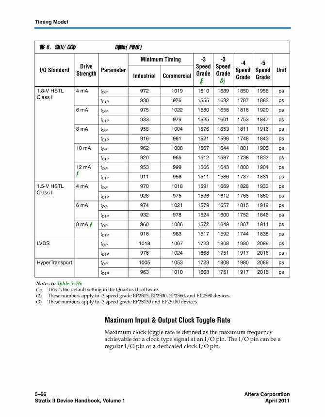
5–66 Altera CorporationStratix II Device Handbook, Volume 1 April 2011
Timing Model
Maximum Input & Output Clock Toggle Rate
Maximum clock toggle rate is defined as the maximum frequency achievable for a clock type signal at an I/O pin. The I/O pin can be a regular I/O pin or a dedicated clock I/O pin.
1.8-V HSTL Class I
4 mA tO P 972 1019 1610 1689 1850 1956 ps
tD I P 930 976 1555 1632 1787 1883 ps
6 mA tO P 975 1022 1580 1658 1816 1920 ps
tD I P 933 979 1525 1601 1753 1847 ps
8 mA tO P 958 1004 1576 1653 1811 1916 ps
tD I P 916 961 1521 1596 1748 1843 ps
10 mA tO P 962 1008 1567 1644 1801 1905 ps
tD I P 920 965 1512 1587 1738 1832 ps
12 mA (1)
tO P 953 999 1566 1643 1800 1904 ps
tD I P 911 956 1511 1586 1737 1831 ps
1.5-V HSTL Class I
4 mA tO P 970 1018 1591 1669 1828 1933 ps
tD I P 928 975 1536 1612 1765 1860 ps
6 mA tO P 974 1021 1579 1657 1815 1919 ps
tD I P 932 978 1524 1600 1752 1846 ps
8 mA (1) tO P 960 1006 1572 1649 1807 1911 ps
tD I P 918 963 1517 1592 1744 1838 ps
LVDS tO P 1018 1067 1723 1808 1980 2089 ps
tD I P 976 1024 1668 1751 1917 2016 ps
HyperTransport tO P 1005 1053 1723 1808 1980 2089 ps
tD I P 963 1010 1668 1751 1917 2016 ps
Notes to Table 5–76:(1) This is the default setting in the Quartus II software.(2) These numbers apply to -3 speed grade EP2S15, EP2S30, EP2S60, and EP2S90 devices.(3) These numbers apply to -3 speed grade EP2S130 and EP2S180 devices.
Table 5–76. Stratix II I/O Output Delay for Row Pins (Part 3 of 3)
I/O Standard Drive Strength Parameter
Minimum Timing -3 Speed Grade
(2)
-3 Speed Grade
(3)
-4 Speed Grade
-5 Speed Grade
Unit Industrial Commercial

Altera Corporation 5–67April 2011 Stratix II Device Handbook, Volume 1
DC & Switching Characteristics
The maximum clock toggle rate is different from the maximum data bit rate. If the maximum clock toggle rate on a regular I/O pin is 300 MHz, the maximum data bit rate for dual data rate (DDR) could be potentially as high as 600 Mbps on the same I/O pin.
Table 5–77 specifies the maximum input clock toggle rates. Table 5–78 specifies the maximum output clock toggle rates at 0pF load. Table 5–79 specifies the derating factors for the output clock toggle rate for a non 0pF load.
To calculate the output toggle rate for a non 0pF load, use this formula:
The toggle rate for a non 0pF load
= 1000 / (1000/ toggle rate at 0pF load + derating factor * load value in pF /1000)
For example, the output toggle rate at 0pF load for SSTL-18 Class II 20mA I/O standard is 550 MHz on a -3 device clock output pin. The derating factor is 94ps/pF. For a 10pF load the toggle rate is calculated as:
1000 / (1000/550 + 94 × 10 /1000) = 363 (MHz)
Tables 5–77 through 5–79 show the I/O toggle rates for Stratix II devices.
Table 5–77. Maximum Input Toggle Rate on Stratix II Devices (Part 1 of 2)
Input I/O StandardColumn I/O Pins (MHz) Row I/O Pins (MHz) Dedicated Clock Inputs
(MHz)
-3 -4 -5 -3 -4 -5 -3 -4 -5
LVTTL 500 500 450 500 500 450 500 500 400
2.5-V LVTTL/CMOS 500 500 450 500 500 450 500 500 400
1.8-V LVTTL/CMOS 500 500 450 500 500 450 500 500 400
1.5-V LVTTL/CMOS 500 500 450 500 500 450 500 500 400
LVCMOS 500 500 450 500 500 450 500 500 400
SSTL-2 Class I 500 500 500 500 500 500 500 500 500
SSTL-2 Class II 500 500 500 500 500 500 500 500 500
SSTL-18 Class I 500 500 500 500 500 500 500 500 500
SSTL-18 Class II 500 500 500 500 500 500 500 500 500
1.5-V HSTL Class I 500 500 500 500 500 500 500 500 500
1.5-V HSTL Class II 500 500 500 500 500 500 500 500 500
1.8-V HSTL Class I 500 500 500 500 500 500 500 500 500

5–68 Altera CorporationStratix II Device Handbook, Volume 1 April 2011
Timing Model
1.8-V HSTL Class II 500 500 500 500 500 500 500 500 500
PCI (1) 500 500 450 - - - 500 500 400
PCI-X (1) 500 500 450 - - - 500 500 400
1.2-V HSTL (2) 280 - - - - - 280 - -
Differential SSTL-2 Class I (1), (3)
500 500 500 - - - 500 500 500
Differential SSTL-2 Class II (1), (3)
500 500 500 - - - 500 500 500
Differential SSTL-18 Class I (1), (3)
500 500 500 - - - 500 500 500
Differential SSTL-18 Class II (1), (3)
500 500 500 - - - 500 500 500
1.8-V Differential HSTL Class I (1), (3)
500 500 500 - - - 500 500 500
1.8-V Differential HSTL Class II (1), (3)
500 500 500 - - - 500 500 500
1.5-V Differential HSTL Class I (1), (3)
500 500 500 - - - 500 500 500
1.5-V Differential HSTL Class II (1), (3)
500 500 500 - - - 500 500 500
HyperTransport technology (4)
- - - 520 520 420 717 717 640
LVPECL (1) - - - - - - 450 450 400
LVDS (5) - - - 520 520 420 717 717 640
LVDS (6) - - - - - - 450 450 400
Notes to Table 5–77:(1) Row clock inputs don’t support PCI, PCI-X, LVPECL, and differential HSTL and SSTL standards.(2) 1.2-V HSTL is only supported on column I/O pins.(3) Differential HSTL and SSTL standards are only supported on column clock and DQS inputs.(4) HyperTransport technology is only supported on row I/O and row dedicated clock input pins.(5) These numbers apply to I/O pins and dedicated clock pins in the left and right I/O banks.(6) These numbers apply to dedicated clock pins in the top and bottom I/O banks.
Table 5–77. Maximum Input Toggle Rate on Stratix II Devices (Part 2 of 2)
Input I/O StandardColumn I/O Pins (MHz) Row I/O Pins (MHz) Dedicated Clock Inputs
(MHz)
-3 -4 -5 -3 -4 -5 -3 -4 -5
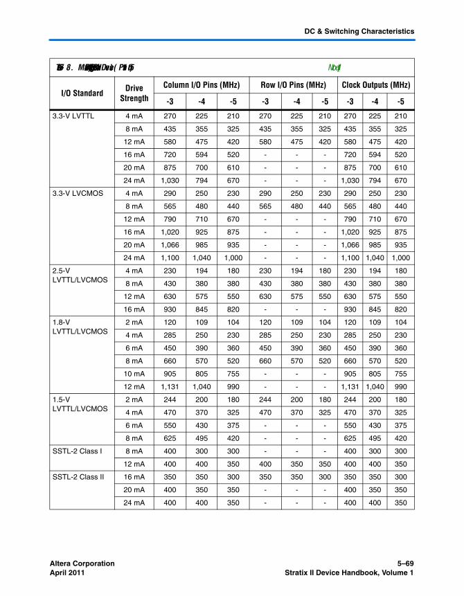
Altera Corporation 5–69April 2011 Stratix II Device Handbook, Volume 1
DC & Switching Characteristics
Table 5–78. Maximum Output Toggle Rate on Stratix II Devices (Part 1 of 5) Note (1)
I/O Standard Drive Strength
Column I/O Pins (MHz) Row I/O Pins (MHz) Clock Outputs (MHz)
-3 -4 -5 -3 -4 -5 -3 -4 -5
3.3-V LVTTL 4 mA 270 225 210 270 225 210 270 225 210
8 mA 435 355 325 435 355 325 435 355 325
12 mA 580 475 420 580 475 420 580 475 420
16 mA 720 594 520 - - - 720 594 520
20 mA 875 700 610 - - - 875 700 610
24 mA 1,030 794 670 - - - 1,030 794 670
3.3-V LVCMOS 4 mA 290 250 230 290 250 230 290 250 230
8 mA 565 480 440 565 480 440 565 480 440
12 mA 790 710 670 - - - 790 710 670
16 mA 1,020 925 875 - - - 1,020 925 875
20 mA 1,066 985 935 - - - 1,066 985 935
24 mA 1,100 1,040 1,000 - - - 1,100 1,040 1,000
2.5-V LVTTL/LVCMOS
4 mA 230 194 180 230 194 180 230 194 180
8 mA 430 380 380 430 380 380 430 380 380
12 mA 630 575 550 630 575 550 630 575 550
16 mA 930 845 820 - - - 930 845 820
1.8-V LVTTL/LVCMOS
2 mA 120 109 104 120 109 104 120 109 104
4 mA 285 250 230 285 250 230 285 250 230
6 mA 450 390 360 450 390 360 450 390 360
8 mA 660 570 520 660 570 520 660 570 520
10 mA 905 805 755 - - - 905 805 755
12 mA 1,131 1,040 990 - - - 1,131 1,040 990
1.5-V LVTTL/LVCMOS
2 mA 244 200 180 244 200 180 244 200 180
4 mA 470 370 325 470 370 325 470 370 325
6 mA 550 430 375 - - - 550 430 375
8 mA 625 495 420 - - - 625 495 420
SSTL-2 Class I 8 mA 400 300 300 - - - 400 300 300
12 mA 400 400 350 400 350 350 400 400 350
SSTL-2 Class II 16 mA 350 350 300 350 350 300 350 350 300
20 mA 400 350 350 - - - 400 350 350
24 mA 400 400 350 - - - 400 400 350

5–70 Altera CorporationStratix II Device Handbook, Volume 1 April 2011
Timing Model
SSTL-18 Class I 4 mA 200 150 150 200 150 150 200 150 150
6 mA 350 250 200 350 250 200 350 250 200
8 mA 450 300 300 450 300 300 450 300 300
10 mA 500 400 400 500 400 400 500 400 400
12 mA 700 550 400 - - - 650 550 400
SSTL-18 Class II 8 mA 200 200 150 - - - 200 200 150
16 mA 400 350 350 - - - 400 350 350
18 mA 450 400 400 - - - 450 400 400
20 mA 550 500 450 - - - 550 500 450
1.8-V HSTL Class I
4 mA 300 300 300 300 300 300 300 300 300
6 mA 500 450 450 500 450 450 500 450 450
8 mA 650 600 600 650 600 600 650 600 600
10 mA 700 650 600 700 650 600 700 650 600
12 mA 700 700 650 700 700 650 700 700 650
1.8-V HSTL Class II
16 mA 500 500 450 - - - 500 500 450
18 mA 550 500 500 - - - 550 500 500
20 mA 650 550 550 - - - 550 550 550
1.5-V HSTL Class I
4 mA 350 300 300 350 300 300 350 300 300
6 mA 500 500 450 500 500 450 500 500 450
8 mA 700 650 600 700 650 600 700 650 600
10 mA 700 700 650 - - - 700 700 650
12 mA 700 700 700 - - - 700 700 700
1.5-V HSTL Class II
16 mA 600 600 550 - - - 600 600 550
18 mA 650 600 600 - - - 650 600 600
20 mA 700 650 600 - - - 700 650 600
Differential SSTL-2 Class I (3)
8 mA 400 300 300 400 300 300 400 300 300
12 mA 400 400 350 400 400 350 400 400 350
Differential SSTL-2 Class II (3)
16 mA 350 350 300 350 350 300 350 350 300
20 mA 400 350 350 350 350 297 400 350 350
24 mA 400 400 350 - - - 400 400 350
Table 5–78. Maximum Output Toggle Rate on Stratix II Devices (Part 2 of 5) Note (1)
I/O Standard Drive Strength
Column I/O Pins (MHz) Row I/O Pins (MHz) Clock Outputs (MHz)
-3 -4 -5 -3 -4 -5 -3 -4 -5

Altera Corporation 5–71April 2011 Stratix II Device Handbook, Volume 1
DC & Switching Characteristics
Differential SSTL-18 Class I (3)
4 mA 200 150 150 200 150 150 200 150 150
6 mA 350 250 200 350 250 200 350 250 200
8 mA 450 300 300 450 300 300 450 300 300
10 mA 500 400 400 500 400 400 500 400 400
12 mA 700 550 400 350 350 297 650 550 400
Differential SSTL-18 Class II (3)
8 mA 200 200 150 - - - 200 200 150
16 mA 400 350 350 - - - 400 350 350
18 mA 450 400 400 - - - 450 400 400
20 mA 550 500 450 - - - 550 500 450
1.8-V Differential HSTL Class I (3)
4 mA 300 300 300 - - - 300 300 300
6 mA 500 450 450 - - - 500 450 450
8 mA 650 600 600 - - - 650 600 600
10 mA 700 650 600 - - - 700 650 600
12 mA 700 700 650 - - - 700 700 650
1.8-V Differential HSTL Class II (3)
16 mA 500 500 450 - - - 500 500 450
18 mA 550 500 500 - - - 550 500 500
20 mA 650 550 550 - - - 550 550 550
1.5-V Differential HSTL Class I (3)
4 mA 350 300 300 - - - 350 300 300
6 mA 500 500 450 - - - 500 500 450
8 mA 700 650 600 - - - 700 650 600
10 mA 700 700 650 - - - 700 700 650
12 mA 700 700 700 - - - 700 700 700
1.5-V Differential HSTL Class II (3)
16 mA 600 600 550 - - - 600 600 550
18 mA 650 600 600 - - - 650 600 600
20 mA 700 650 600 - - - 700 650 600
3.3-V PCI 1,000 790 670 - - - 1,000 790 670
3.3-V PCI-X 1,000 790 670 - - - 1,000 790 670
LVDS (6) - - - 500 500 500 450 400 300
HyperTransport technology (4), (6)
500 500 500 - - -
LVPECL (5) - - - - - - 450 400 300
3.3-V LVTTL OCT 50 Ω 400 400 350 400 400 350 400 400 350
2.5-V LVTTL OCT 50 Ω 350 350 300 350 350 300 350 350 300
Table 5–78. Maximum Output Toggle Rate on Stratix II Devices (Part 3 of 5) Note (1)
I/O Standard Drive Strength
Column I/O Pins (MHz) Row I/O Pins (MHz) Clock Outputs (MHz)
-3 -4 -5 -3 -4 -5 -3 -4 -5

5–72 Altera CorporationStratix II Device Handbook, Volume 1 April 2011
Timing Model
1.8-V LVTTL OCT 50 Ω 700 550 450 700 550 450 700 550 450
3.3-V LVCMOS OCT 50 Ω 350 350 300 350 350 300 350 350 300
1.5-V LVCMOS OCT 50 Ω 550 450 400 550 450 400 550 450 400
SSTL-2 Class I OCT 50 Ω 600 500 500 600 500 500 600 500 500
SSTL-2 Class II OCT 25 Ω 600 550 500 600 550 500 600 550 500
SSTL-18 Class I OCT 50 Ω 560 400 350 590 400 350 450 400 350
SSTL-18 Class II OCT 25 Ω 550 500 450 - - - 550 500 450
1.2-V HSTL (2) OCT 50 Ω 280 - - - - - 280 - -
1.5-V HSTL Class I
OCT 50 Ω 600 550 500 600 550 500 600 550 500
1.8-V HSTL Class I
OCT 50 Ω 650 600 600 650 600 600 650 600 600
1.8-V HSTL Class II
OCT 25 Ω 500 500 450 - - - 500 500 450
Differential SSTL-2 Class I
OCT 50 Ω 600 500 500 600 500 500 600 500 500
Differential SSTL-2 Class II
OCT 25 Ω 600 550 500 600 550 500 600 550 500
Differential SSTL-18 Class I
OCT 50 Ω 560 400 350 590 400 350 560 400 350
Differential SSTL-18 Class II
OCT 25 Ω 550 500 450 - - - 550 500 450
1.8-V Differential HSTL Class I
OCT 50 Ω 650 600 600 650 600 600 650 600 600
1.8-V Differential HSTL Class II
OCT 25 Ω 500 500 450 - - - 500 500 450
1.5-V Differential HSTL Class I
OCT 50 Ω 600 550 500 600 550 500 600 550 500
Table 5–78. Maximum Output Toggle Rate on Stratix II Devices (Part 4 of 5) Note (1)
I/O Standard Drive Strength
Column I/O Pins (MHz) Row I/O Pins (MHz) Clock Outputs (MHz)
-3 -4 -5 -3 -4 -5 -3 -4 -5

Altera Corporation 5–73April 2011 Stratix II Device Handbook, Volume 1
DC & Switching Characteristics
1.2-V Differential HSTL
OCT 50 Ω 280 - - - - - 280 - -
Notes to Table 5–78:(1) The toggle rate applies to 0-pF output load for all I/O standards except for LVDS and HyperTransport technology
on row I/O pins. For LVDS and HyperTransport technology on row I/O pins, the toggle rates apply to load from 0 to 5pF.
(2) 1.2-V HSTL is only supported on column I/O pins in I/O banks 4, 7, and 8.(3) Differential HSTL and SSTL is only supported on column clock and DQS outputs.(4) HyperTransport technology is only supported on row I/O and row dedicated clock input pins.(5) LVPECL is only supported on column clock pins.(6) Refer to Tables 5–81 through 5–91 if using SERDES block. Use the toggle rate values from the clock output column
for PLL output.
Table 5–79. Maximum Output Clock Toggle Rate Derating Factors (Part 1 of 5)
I/O Standard Drive Strength
Maximum Output Clock Toggle Rate Derating Factors (ps/pF)
Column I/O Pins Row I/O Pins Dedicated Clock Outputs
-3 -4 -5 -3 -4 -5 -3 -4 -5
3.3-V LVTTL 4 mA 478 510 510 478 510 510 466 510 510
8 mA 260 333 333 260 333 333 291 333 333
12 mA 213 247 247 213 247 247 211 247 247
16 mA 136 197 197 - - - 166 197 197
20 mA 138 187 187 - - - 154 187 187
24 mA 134 177 177 - - - 143 177 177
3.3-V LVCMOS 4 mA 377 391 391 377 391 391 377 391 391
8 mA 206 212 212 206 212 212 178 212 212
12 mA 141 145 145 - - - 115 145 145
16 mA 108 111 111 - - - 86 111 111
20 mA 83 88 88 - - - 79 88 88
24 mA 65 72 72 - - - 74 72 72
2.5-V LVTTL/LVCMOS
4 mA 387 427 427 387 427 427 391 427 427
8 mA 163 224 224 163 224 224 170 224 224
12 mA 142 203 203 142 203 203 152 203 203
16 mA 120 182 182 - - - 134 182 182
Table 5–78. Maximum Output Toggle Rate on Stratix II Devices (Part 5 of 5) Note (1)
I/O Standard Drive Strength
Column I/O Pins (MHz) Row I/O Pins (MHz) Clock Outputs (MHz)
-3 -4 -5 -3 -4 -5 -3 -4 -5

5–74 Altera CorporationStratix II Device Handbook, Volume 1 April 2011
Timing Model
1.8-V LVTTL/LVCMOS
2 mA 951 1421 1421 951 1421 1421 904 1421 1421
4 mA 405 516 516 405 516 516 393 516 516
6 mA 261 325 325 261 325 325 253 325 325
8 mA 223 274 274 223 274 274 224 274 274
10 mA 194 236 236 - - - 199 236 236
12 mA 174 209 209 - - - 180 209 209
1.5-V LVTTL/LVCMOS
2 mA 652 963 963 652 963 963 618 963 963
4 mA 333 347 347 333 347 347 270 347 347
6 mA 182 247 247 - - - 198 247 247
8 mA 135 194 194 - - - 155 194 194
SSTL-2 Class I 8 mA 364 680 680 364 680 680 350 680 680
12 mA 163 207 207 163 207 207 188 207 207
SSTL-2 Class II 16 mA 118 147 147 118 147 147 94 147 147
20 mA 99 122 122 - - - 87 122 122
24 mA 91 116 116 - - - 85 116 116
SSTL-18 Class I 4 mA 458 570 570 458 570 570 505 570 570
6 mA 305 380 380 305 380 380 336 380 380
8 mA 225 282 282 225 282 282 248 282 282
10 mA 167 220 220 167 220 220 190 220 220
12 mA 129 175 175 - - - 148 175 175
SSTL-18 Class II 8 mA 173 206 206 - - - 155 206 206
16 mA 150 160 160 - - - 140 160 160
18 mA 120 130 130 - - - 110 130 130
20 mA 109 127 127 - - - 94 127 127
SSTL-2 Class I 8 mA 364 680 680 364 680 680 350 680 680
12 mA 163 207 207 163 207 207 188 207 207
SSTL-2 Class II 16 mA 118 147 147 118 147 147 94 147 147
20 mA 99 122 122 - - - 87 122 122
24 mA 91 116 116 - - - 85 116 116
Table 5–79. Maximum Output Clock Toggle Rate Derating Factors (Part 2 of 5)
I/O Standard Drive Strength
Maximum Output Clock Toggle Rate Derating Factors (ps/pF)
Column I/O Pins Row I/O Pins Dedicated Clock Outputs
-3 -4 -5 -3 -4 -5 -3 -4 -5

Altera Corporation 5–75April 2011 Stratix II Device Handbook, Volume 1
DC & Switching Characteristics
SSTL-18 Class I 4 mA 458 570 570 458 570 570 505 570 570
6 mA 305 380 380 305 380 380 336 380 380
8 mA 225 282 282 225 282 282 248 282 282
10 mA 167 220 220 167 220 220 190 220 220
12 mA 129 175 175 - - - 148 175 175
SSTL-18 Class II 8 mA 173 206 206 - - - 155 206 206
16 mA 150 160 160 - - - 140 160 160
18 mA 120 130 130 - - - 110 130 130
20 mA 109 127 127 - - - 94 127 127
1.8-V HSTL Class I
4 mA 245 282 282 245 282 282 229 282 282
6 mA 164 188 188 164 188 188 153 188 188
8 mA 123 140 140 123 140 140 114 140 140
10 mA 110 124 124 110 124 124 108 124 124
12 mA 97 110 110 97 110 110 104 110 110
1.8-V HSTL Class II
16 mA 101 104 104 - - - 99 104 104
18 mA 98 102 102 - - - 93 102 102
20 mA 93 99 99 - - - 88 99 99
1.5-V HSTL Class I
4 mA 168 196 196 168 196 196 188 196 196
6 mA 112 131 131 112 131 131 125 131 131
8 mA 84 99 99 84 99 99 95 99 99
10 mA 87 98 98 - - - 90 98 98
12 mA 86 98 98 - - - 87 98 98
1.5-V HSTL Class II
16 mA 95 101 101 - - - 96 101 101
18 mA 95 100 100 - - - 101 100 100
20 mA 94 101 101 - - - 104 101 101
Differential SSTL-2 Class II (3)
8 mA 364 680 680 - - - 350 680 680
12 mA 163 207 207 - - - 188 207 207
16 mA 118 147 147 - - - 94 147 147
20 mA 99 122 122 - - - 87 122 122
24 mA 91 116 116 - - - 85 116 116
Table 5–79. Maximum Output Clock Toggle Rate Derating Factors (Part 3 of 5)
I/O Standard Drive Strength
Maximum Output Clock Toggle Rate Derating Factors (ps/pF)
Column I/O Pins Row I/O Pins Dedicated Clock Outputs
-3 -4 -5 -3 -4 -5 -3 -4 -5

5–76 Altera CorporationStratix II Device Handbook, Volume 1 April 2011
Timing Model
Differential SSTL-18 Class I (3)
4 mA 458 570 570 - - - 505 570 570
6 mA 305 380 380 - - - 336 380 380
8 mA 225 282 282 - - - 248 282 282
10 mA 167 220 220 - - - 190 220 220
12 mA 129 175 175 - - - 148 175 175
Differential SSTL-18 Class II (3)
8 mA 173 206 206 - - - 155 206 206
16 mA 150 160 160 - - - 140 160 160
18 mA 120 130 130 - - - 110 130 130
20 mA 109 127 127 - - - 94 127 127
1.8-V Differential HSTL Class I (3)
4 mA 245 282 282 - - - 229 282 282
6 mA 164 188 188 - - - 153 188 188
8 mA 123 140 140 - - - 114 140 140
10 mA 110 124 124 - - - 108 124 124
12 mA 97 110 110 - - - 104 110 110
1.8-V Differential HSTL Class II (3)
16 mA 101 104 104 - - - 99 104 104
18 mA 98 102 102 - - - 93 102 102
20 mA 93 99 99 - - - 88 99 99
1.5-V Differential HSTL Class I (3)
4 mA 168 196 196 - - - 188 196 196
6 mA 112 131 131 - - - 125 131 131
8 mA 84 99 99 - - - 95 99 99
10 mA 87 98 98 - - - 90 98 98
12 mA 86 98 98 - - - 87 98 98
1.5-V Differential HSTL Class II (3)
16 mA 95 101 101 - - - 96 101 101
18 mA 95 100 100 - - - 101 100 100
20 mA 94 101 101 - - - 104 101 101
3.3-V PCI 134 177 177 - - - 143 177 177
3.3-V PCI-X 134 177 177 - - - 143 177 177
LVDS - - - 155 (1) 155 (1)
155 (1)
134 134 134
HyperTransport technology
- - - 155 (1) 155 (1)
155 (1)
- - -
LVPECL (4) - - - - - - 134 134 134
Table 5–79. Maximum Output Clock Toggle Rate Derating Factors (Part 4 of 5)
I/O Standard Drive Strength
Maximum Output Clock Toggle Rate Derating Factors (ps/pF)
Column I/O Pins Row I/O Pins Dedicated Clock Outputs
-3 -4 -5 -3 -4 -5 -3 -4 -5
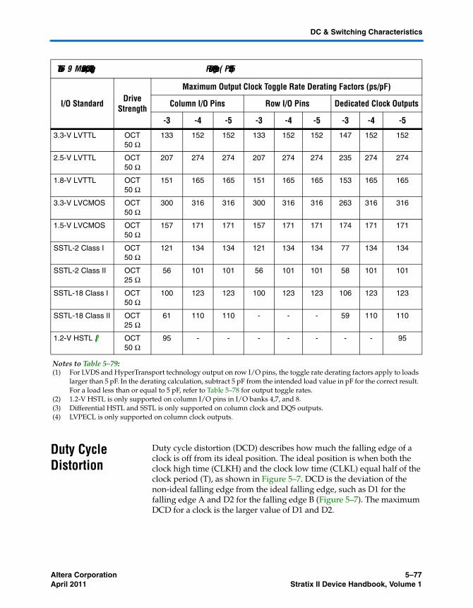
Altera Corporation 5–77April 2011 Stratix II Device Handbook, Volume 1
DC & Switching Characteristics
Duty Cycle Distortion
Duty cycle distortion (DCD) describes how much the falling edge of a clock is off from its ideal position. The ideal position is when both the clock high time (CLKH) and the clock low time (CLKL) equal half of the clock period (T), as shown in Figure 5–7. DCD is the deviation of the non-ideal falling edge from the ideal falling edge, such as D1 for the falling edge A and D2 for the falling edge B (Figure 5–7). The maximum DCD for a clock is the larger value of D1 and D2.
3.3-V LVTTL OCT 50 Ω
133 152 152 133 152 152 147 152 152
2.5-V LVTTL OCT 50 Ω
207 274 274 207 274 274 235 274 274
1.8-V LVTTL OCT 50 Ω
151 165 165 151 165 165 153 165 165
3.3-V LVCMOS OCT 50 Ω
300 316 316 300 316 316 263 316 316
1.5-V LVCMOS OCT 50 Ω
157 171 171 157 171 171 174 171 171
SSTL-2 Class I OCT 50 Ω
121 134 134 121 134 134 77 134 134
SSTL-2 Class II OCT 25 Ω
56 101 101 56 101 101 58 101 101
SSTL-18 Class I OCT 50 Ω
100 123 123 100 123 123 106 123 123
SSTL-18 Class II OCT 25 Ω
61 110 110 - - - 59 110 110
1.2-V HSTL (2) OCT 50 Ω
95 - - - - - - - 95
Notes to Table 5–79:(1) For LVDS and HyperTransport technology output on row I/O pins, the toggle rate derating factors apply to loads
larger than 5 pF. In the derating calculation, subtract 5 pF from the intended load value in pF for the correct result. For a load less than or equal to 5 pF, refer to Table 5–78 for output toggle rates.
(2) 1.2-V HSTL is only supported on column I/O pins in I/O banks 4,7, and 8.(3) Differential HSTL and SSTL is only supported on column clock and DQS outputs.(4) LVPECL is only supported on column clock outputs.
Table 5–79. Maximum Output Clock Toggle Rate Derating Factors (Part 5 of 5)
I/O Standard Drive Strength
Maximum Output Clock Toggle Rate Derating Factors (ps/pF)
Column I/O Pins Row I/O Pins Dedicated Clock Outputs
-3 -4 -5 -3 -4 -5 -3 -4 -5

5–78 Altera CorporationStratix II Device Handbook, Volume 1 April 2011
Duty Cycle Distortion
Figure 5–7. Duty Cycle Distortion
DCD expressed in absolution derivation, for example, D1 or D2 in Figure 5–7, is clock-period independent. DCD can also be expressed as a percentage, and the percentage number is clock-period dependent. DCD as a percentage is defined as
(T/2 – D1) / T (the low percentage boundary)
(T/2 + D2) / T (the high percentage boundary)
DCD Measurement Techniques
DCD is measured at an FPGA output pin driven by registers inside the corresponding I/O element (IOE) block. When the output is a single data rate signal (non-DDIO), only one edge of the register input clock (positive or negative) triggers output transitions (Figure 5–8). Therefore, any DCD present on the input clock signal or caused by the clock input buffer or different input I/O standard does not transfer to the output signal.
Figure 5–8. DCD Measurement Technique for Non-DDIO (Single-Data Rate) Outputs
CLKH = T/2 CLKL = T/2
D1 D2
Falling Edge A
Ideal Falling Edge
Clock Period (T)
Falling Edge B
D Q
inst
PRN
CLRN
inst1
DFF
INPUTVCC
clk
NOT
OUTPUT output
IOE
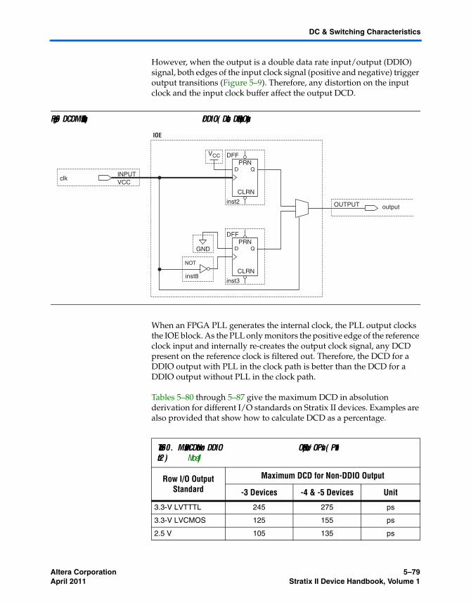
Altera Corporation 5–79April 2011 Stratix II Device Handbook, Volume 1
DC & Switching Characteristics
However, when the output is a double data rate input/output (DDIO) signal, both edges of the input clock signal (positive and negative) trigger output transitions (Figure 5–9). Therefore, any distortion on the input clock and the input clock buffer affect the output DCD.
Figure 5–9. DCD Measurement Technique for DDIO (Double-Data Rate) Outputs
When an FPGA PLL generates the internal clock, the PLL output clocks the IOE block. As the PLL only monitors the positive edge of the reference clock input and internally re-creates the output clock signal, any DCD present on the reference clock is filtered out. Therefore, the DCD for a DDIO output with PLL in the clock path is better than the DCD for a DDIO output without PLL in the clock path.
Tables 5–80 through 5–87 give the maximum DCD in absolution derivation for different I/O standards on Stratix II devices. Examples are also provided that show how to calculate DCD as a percentage.
D Q
inst2
PRN
CLRN
inst8
DFF
INPUTVCC
clk
NOT
OUTPUT output
IOE
D Q
inst3
PRN
CLRN
DFF
VCC
GND
Table 5–80. Maximum DCD for Non-DDIO Output on Row I/O Pins (Part 1 of 2) Note (1)
Row I/O Output Standard
Maximum DCD for Non-DDIO Output
-3 Devices -4 & -5 Devices Unit
3.3-V LVTTTL 245 275 ps
3.3-V LVCMOS 125 155 ps
2.5 V 105 135 ps

5–80 Altera CorporationStratix II Device Handbook, Volume 1 April 2011
Duty Cycle Distortion
Here is an example for calculating the DCD as a percentage for a non-DDIO output on a row I/O on a -3 device:
If the non-DDIO output I/O standard is SSTL-2 Class II, the maximum DCD is 95 ps (see Table 5–80). If the clock frequency is 267 MHz, the clock period T is:
T = 1/ f = 1 / 267 MHz = 3.745 ns = 3745 ps
To calculate the DCD as a percentage:
(T/2 – DCD) / T = (3745ps/2 – 95ps) / 3745ps = 47.5% (for low boundary)
(T/2 + DCD) / T = (3745ps/2 + 95ps) / 3745ps = 52.5% (for high boundary)
1.8 V 180 180 ps
1.5-V LVCMOS 165 195 ps
SSTL-2 Class I 115 145 ps
SSTL-2 Class II 95 125 ps
SSTL-18 Class I 55 85 ps
1.8-V HSTL Class I 80 100 ps
1.5-V HSTL Class I 85 115 ps
LVDS/ HyperTransport technology
55 80 ps
Note to Table 5–80:(1) The DCD specification is based on a no logic array noise condition.
Table 5–80. Maximum DCD for Non-DDIO Output on Row I/O Pins (Part 2 of 2) Note (1)
Row I/O Output Standard
Maximum DCD for Non-DDIO Output
-3 Devices -4 & -5 Devices Unit
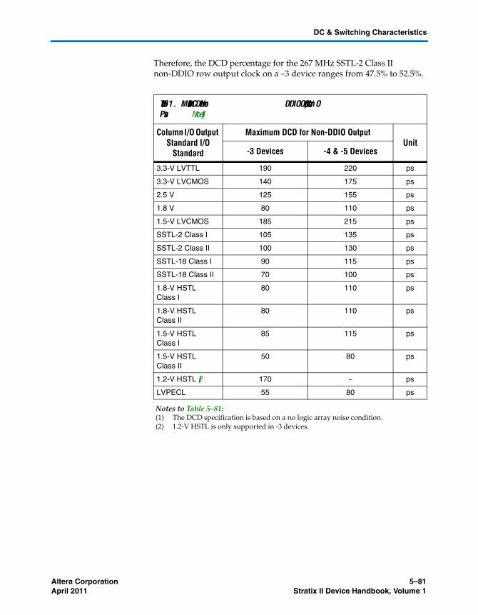
Altera Corporation 5–81April 2011 Stratix II Device Handbook, Volume 1
DC & Switching Characteristics
Therefore, the DCD percentage for the 267 MHz SSTL-2 Class II non-DDIO row output clock on a –3 device ranges from 47.5% to 52.5%.
Table 5–81. Maximum DCD for Non-DDIO Output on Column I/O Pins Note (1)
Column I/O Output Standard I/O
Standard
Maximum DCD for Non-DDIO OutputUnit
-3 Devices -4 & -5 Devices
3.3-V LVTTL 190 220 ps
3.3-V LVCMOS 140 175 ps
2.5 V 125 155 ps
1.8 V 80 110 ps
1.5-V LVCMOS 185 215 ps
SSTL-2 Class I 105 135 ps
SSTL-2 Class II 100 130 ps
SSTL-18 Class I 90 115 ps
SSTL-18 Class II 70 100 ps
1.8-V HSTL Class I
80 110 ps
1.8-V HSTL Class II
80 110 ps
1.5-V HSTL Class I
85 115 ps
1.5-V HSTL Class II
50 80 ps
1.2-V HSTL (2) 170 - ps
LVPECL 55 80 ps
Notes to Table 5–81:(1) The DCD specification is based on a no logic array noise condition.(2) 1.2-V HSTL is only supported in -3 devices.

5–82 Altera CorporationStratix II Device Handbook, Volume 1 April 2011
Duty Cycle Distortion
Here is an example for calculating the DCD in percentage for a DDIO output on a row I/O on a -3 device:
If the input I/O standard is SSTL-2 and the DDIO output I/O standard is SSTL-2 Class II, the maximum DCD is 60 ps (see Table 5–82). If the clock frequency is 267 MHz, the clock period T is:
T = 1/ f = 1 / 267 MHz = 3.745 ns = 3745 ps
Calculate the DCD as a percentage:
(T/2 – DCD) / T = (3745ps/2 – 60ps) / 3745ps = 48.4% (for low boundary)
(T/2 + DCD) / T = (3745 ps/2 + 60 ps) / 3745ps = 51.6% (for high boundary)
Table 5–82. Maximum DCD for DDIO Output on Row I/O Pins Without PLL in the Clock Path for -3 Devices Notes (1), (2)
Row DDIO Output I/O Standard
Maximum DCD Based on I/O Standard of Input Feeding the DDIO Clock Port (No PLL in Clock Path)
UnitTTL/CMOS SSTL-2 SSTL/HSTLLVDS/
HyperTransport Technology
3.3 & 2.5 V 1.8 & 1.5 V 2.5 V 1.8 & 1.5 V 3.3 V
3.3-V LVTTL 260 380 145 145 110 ps
3.3-V LVCMOS 210 330 100 100 65 ps
2.5 V 195 315 85 85 75 ps
1.8 V 150 265 85 85 120 ps
1.5-V LVCMOS 255 370 140 140 105 ps
SSTL-2 Class I 175 295 65 65 70 ps
SSTL-2 Class II 170 290 60 60 75 ps
SSTL-18 Class I 155 275 55 50 90 ps
1.8-V HSTL Class I 150 270 60 60 95 ps
1.5-V HSTL Class I 150 270 55 55 90 ps
LVDS/ HyperTransport technology
180 180 180 180 180 ps
Notes to Table 5–82:(1) The information in Table 5–82 assumes the input clock has zero DCD.(2) The DCD specification is based on a no logic array noise condition.
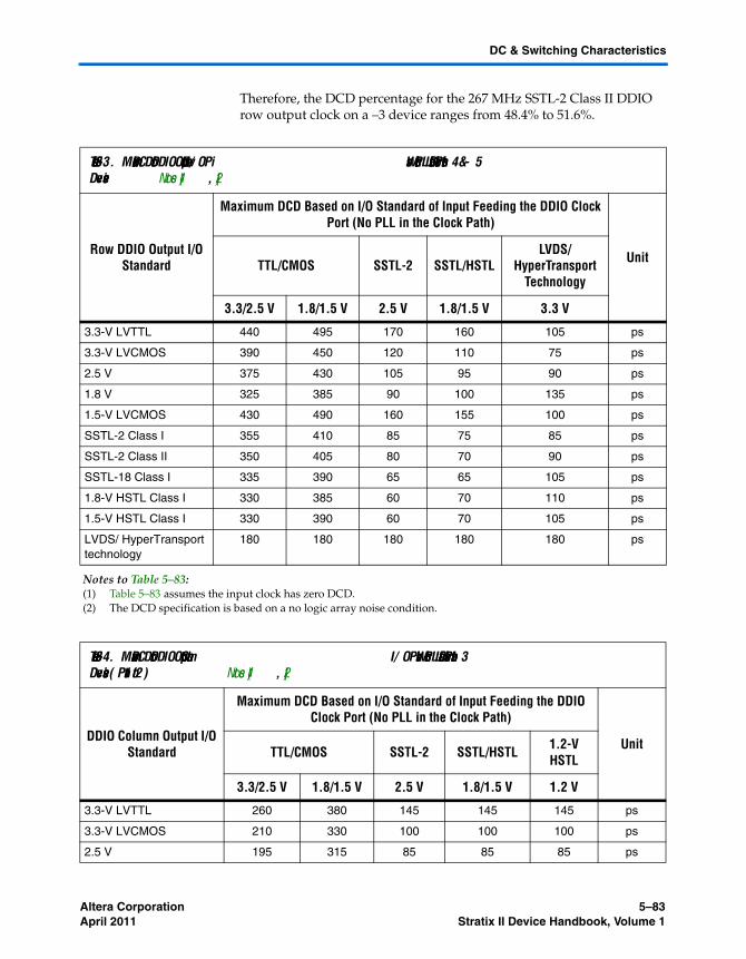
Altera Corporation 5–83April 2011 Stratix II Device Handbook, Volume 1
DC & Switching Characteristics
Therefore, the DCD percentage for the 267 MHz SSTL-2 Class II DDIO row output clock on a –3 device ranges from 48.4% to 51.6%.
Table 5–83. Maximum DCD for DDIO Output on Row I/O Pins Without PLL in the Clock Path for -4 & -5 Devices Notes (1), (2)
Row DDIO Output I/O Standard
Maximum DCD Based on I/O Standard of Input Feeding the DDIO Clock Port (No PLL in the Clock Path)
UnitTTL/CMOS SSTL-2 SSTL/HSTLLVDS/
HyperTransport Technology
3.3/2.5 V 1.8/1.5 V 2.5 V 1.8/1.5 V 3.3 V
3.3-V LVTTL 440 495 170 160 105 ps
3.3-V LVCMOS 390 450 120 110 75 ps
2.5 V 375 430 105 95 90 ps
1.8 V 325 385 90 100 135 ps
1.5-V LVCMOS 430 490 160 155 100 ps
SSTL-2 Class I 355 410 85 75 85 ps
SSTL-2 Class II 350 405 80 70 90 ps
SSTL-18 Class I 335 390 65 65 105 ps
1.8-V HSTL Class I 330 385 60 70 110 ps
1.5-V HSTL Class I 330 390 60 70 105 ps
LVDS/ HyperTransport technology
180 180 180 180 180 ps
Notes to Table 5–83:(1) Table 5–83 assumes the input clock has zero DCD.(2) The DCD specification is based on a no logic array noise condition.
Table 5–84. Maximum DCD for DDIO Output on Column I/O Pins Without PLL in the Clock Path for -3 Devices (Part 1 of 2) Notes (1), (2)
DDIO Column Output I/O Standard
Maximum DCD Based on I/O Standard of Input Feeding the DDIO Clock Port (No PLL in the Clock Path)
UnitTTL/CMOS SSTL-2 SSTL/HSTL 1.2-V HSTL
3.3/2.5 V 1.8/1.5 V 2.5 V 1.8/1.5 V 1.2 V
3.3-V LVTTL 260 380 145 145 145 ps
3.3-V LVCMOS 210 330 100 100 100 ps
2.5 V 195 315 85 85 85 ps
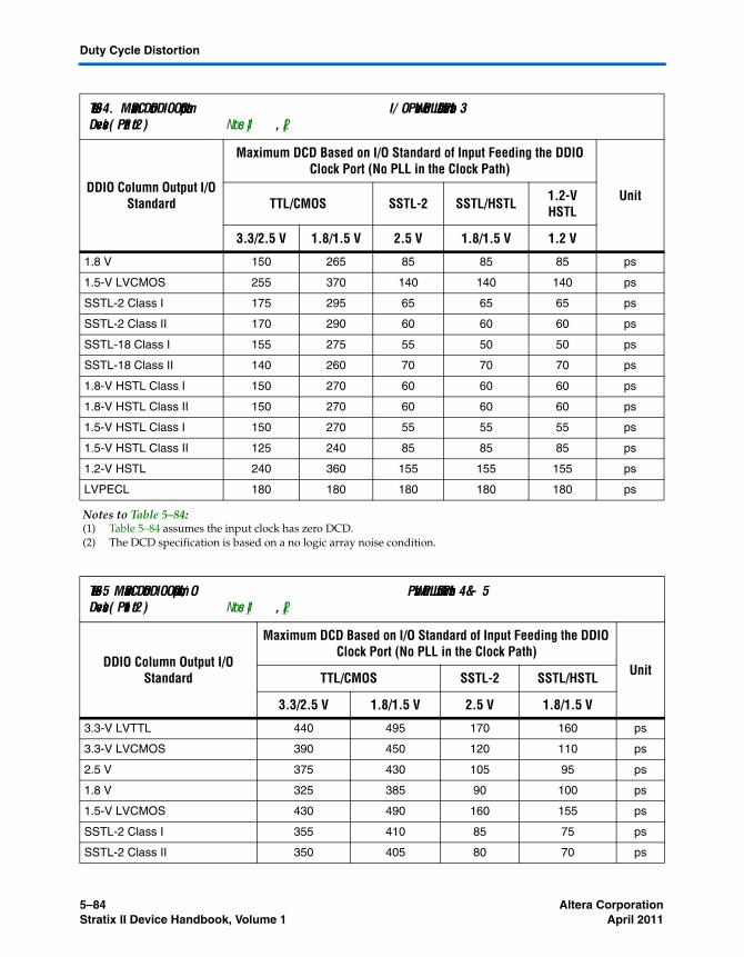
5–84 Altera CorporationStratix II Device Handbook, Volume 1 April 2011
Duty Cycle Distortion
1.8 V 150 265 85 85 85 ps
1.5-V LVCMOS 255 370 140 140 140 ps
SSTL-2 Class I 175 295 65 65 65 ps
SSTL-2 Class II 170 290 60 60 60 ps
SSTL-18 Class I 155 275 55 50 50 ps
SSTL-18 Class II 140 260 70 70 70 ps
1.8-V HSTL Class I 150 270 60 60 60 ps
1.8-V HSTL Class II 150 270 60 60 60 ps
1.5-V HSTL Class I 150 270 55 55 55 ps
1.5-V HSTL Class II 125 240 85 85 85 ps
1.2-V HSTL 240 360 155 155 155 ps
LVPECL 180 180 180 180 180 ps
Notes to Table 5–84:(1) Table 5–84 assumes the input clock has zero DCD.(2) The DCD specification is based on a no logic array noise condition.
Table 5–85. Maximum DCD for DDIO Output on Column I/O Pins Without PLL in the Clock Path for -4 & -5 Devices (Part 1 of 2) Notes (1), (2)
DDIO Column Output I/O Standard
Maximum DCD Based on I/O Standard of Input Feeding the DDIO Clock Port (No PLL in the Clock Path)
UnitTTL/CMOS SSTL-2 SSTL/HSTL
3.3/2.5 V 1.8/1.5 V 2.5 V 1.8/1.5 V
3.3-V LVTTL 440 495 170 160 ps
3.3-V LVCMOS 390 450 120 110 ps
2.5 V 375 430 105 95 ps
1.8 V 325 385 90 100 ps
1.5-V LVCMOS 430 490 160 155 ps
SSTL-2 Class I 355 410 85 75 ps
SSTL-2 Class II 350 405 80 70 ps
Table 5–84. Maximum DCD for DDIO Output on Column I/O Pins Without PLL in the Clock Path for -3 Devices (Part 2 of 2) Notes (1), (2)
DDIO Column Output I/O Standard
Maximum DCD Based on I/O Standard of Input Feeding the DDIO Clock Port (No PLL in the Clock Path)
UnitTTL/CMOS SSTL-2 SSTL/HSTL 1.2-V HSTL
3.3/2.5 V 1.8/1.5 V 2.5 V 1.8/1.5 V 1.2 V

Altera Corporation 5–85April 2011 Stratix II Device Handbook, Volume 1
DC & Switching Characteristics
SSTL-18 Class I 335 390 65 65 ps
SSTL-18 Class II 320 375 70 80 ps
1.8-V HSTL Class I 330 385 60 70 ps
1.8-V HSTL Class II 330 385 60 70 ps
1.5-V HSTL Class I 330 390 60 70 ps
1.5-V HSTL Class II 330 360 90 100 ps
1.2-V HSTL 420 470 155 165 ps
LVPECL 180 180 180 180 ps
Notes to Table 5–85:(1) Table 5–85 assumes the input clock has zero DCD.(2) The DCD specification is based on a no logic array noise condition.
Table 5–85. Maximum DCD for DDIO Output on Column I/O Pins Without PLL in the Clock Path for -4 & -5 Devices (Part 2 of 2) Notes (1), (2)
DDIO Column Output I/O Standard
Maximum DCD Based on I/O Standard of Input Feeding the DDIO Clock Port (No PLL in the Clock Path)
UnitTTL/CMOS SSTL-2 SSTL/HSTL
3.3/2.5 V 1.8/1.5 V 2.5 V 1.8/1.5 V
Table 5–86. Maximum DCD for DDIO Output on Row I/O Pins with PLL in the Clock Path (Part 1 of 2) Note (1)
Row DDIO Output I/O Standard
Maximum DCD (PLL Output Clock Feeding DDIO Clock Port) Unit
-3 Device -4 & -5 Device
3.3-V LVTTL 110 105 ps
3.3-V LVCMOS 65 75 ps
2.5V 75 90 ps
1.8V 85 100 ps
1.5-V LVCMOS 105 100 ps
SSTL-2 Class I 65 75 ps
SSTL-2 Class II 60 70 ps
SSTL-18 Class I 50 65 ps
1.8-V HSTL Class I 50 70 ps
1.5-V HSTL Class I 55 70 ps
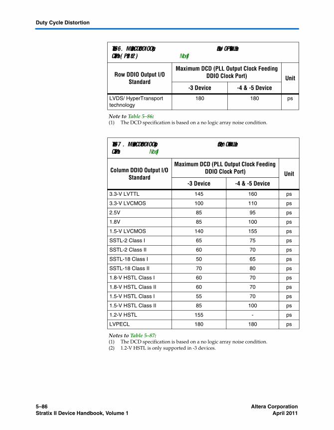
5–86 Altera CorporationStratix II Device Handbook, Volume 1 April 2011
Duty Cycle Distortion
LVDS/ HyperTransport technology
180 180 ps
Note to Table 5–86:(1) The DCD specification is based on a no logic array noise condition.
Table 5–87. Maximum DCD for DDIO Output on Column I/O with PLL in the Clock Path Note (1)
Column DDIO Output I/O Standard
Maximum DCD (PLL Output Clock Feeding DDIO Clock Port) Unit
-3 Device -4 & -5 Device
3.3-V LVTTL 145 160 ps
3.3-V LVCMOS 100 110 ps
2.5V 85 95 ps
1.8V 85 100 ps
1.5-V LVCMOS 140 155 ps
SSTL-2 Class I 65 75 ps
SSTL-2 Class II 60 70 ps
SSTL-18 Class I 50 65 ps
SSTL-18 Class II 70 80 ps
1.8-V HSTL Class I 60 70 ps
1.8-V HSTL Class II 60 70 ps
1.5-V HSTL Class I 55 70 ps
1.5-V HSTL Class II 85 100 ps
1.2-V HSTL 155 - ps
LVPECL 180 180 ps
Notes to Table 5–87:(1) The DCD specification is based on a no logic array noise condition.(2) 1.2-V HSTL is only supported in -3 devices.
Table 5–86. Maximum DCD for DDIO Output on Row I/O Pins with PLL in the Clock Path (Part 2 of 2) Note (1)
Row DDIO Output I/O Standard
Maximum DCD (PLL Output Clock Feeding DDIO Clock Port) Unit
-3 Device -4 & -5 Device

Altera Corporation 5–87April 2011 Stratix II Device Handbook, Volume 1
DC & Switching Characteristics
High-Speed I/O Specifications
Table 5–88 provides high-speed timing specifications definitions.
Table 5–89 shows the high-speed I/O timing specifications for -3 speed grade Stratix II devices.
Table 5–88. High-Speed Timing Specifications & Definitions
High-Speed Timing Specifications Definitions
tC High-speed receiver/transmitter input and output clock period.
fH S C L K High-speed receiver/transmitter input and output clock frequency.
J Deserialization factor (width of parallel data bus).
W PLL multiplication factor.
tR I S E Low-to-high transmission time.
tF A L L High-to-low transmission time.
Timing unit interval (TUI) The timing budget allowed for skew, propagation delays, and data sampling window. (TUI = 1/(Receiver Input Clock Frequency × Multiplication Factor) = tC /w).
fH S D R Maximum/minimum LVDS data transfer rate (fH S D R = 1/TUI), non-DPA.
fH S D R DP A Maximum/minimum LVDS data transfer rate (fH S D R D PA = 1/TUI), DPA.
Channel-to-channel skew (TCCS) The timing difference between the fastest and slowest output edges, including tC O variation and clock skew. The clock is included in the TCCS measurement.
Sampling window (SW) The period of time during which the data must be valid in order to capture it correctly. The setup and hold times determine the ideal strobe position within the sampling window.
Input jitter Peak-to-peak input jitter on high-speed PLLs.
Output jitter Peak-to-peak output jitter on high-speed PLLs.
tDUTY Duty cycle on high-speed transmitter output clock.
tL O C K Lock time for high-speed transmitter and receiver PLLs.
Table 5–89. High-Speed I/O Specifications for -3 Speed Grade (Part 1 of 2) Notes (1), (2)
Symbol Conditions-3 Speed Grade
UnitMin Typ Max
fH S C L K (clock frequency) fH S C L K = fHS D R / W
W = 2 to 32 (LVDS, HyperTransport technology) (3)
16 520 MHz
W = 1 (SERDES bypass, LVDS only) 16 500 MHz
W = 1 (SERDES used, LVDS only) 150 717 MHz
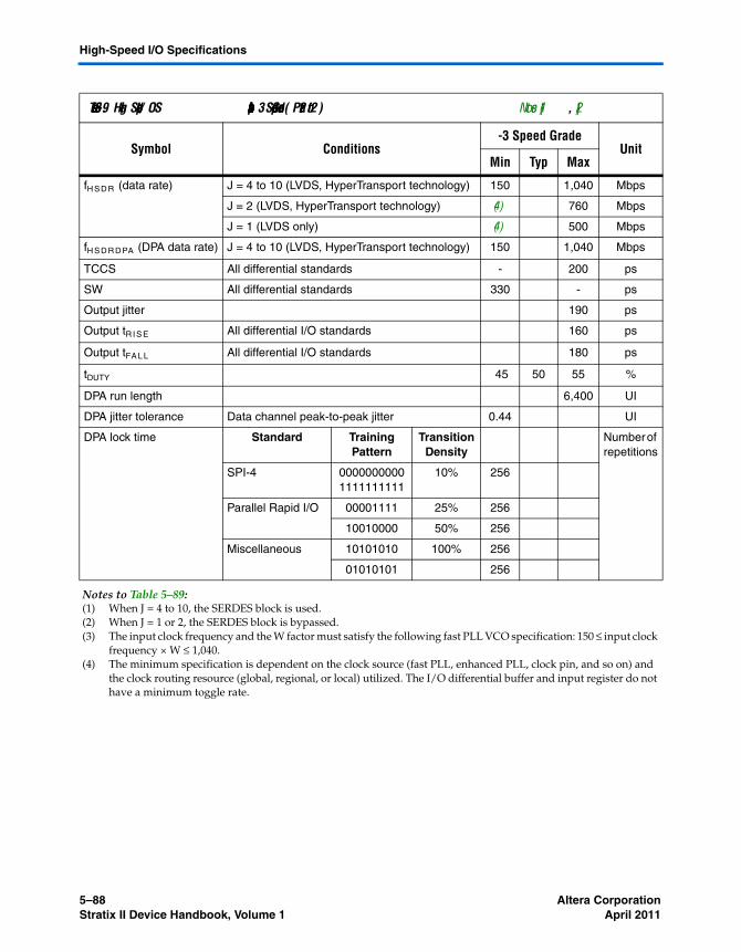
5–88 Altera CorporationStratix II Device Handbook, Volume 1 April 2011
High-Speed I/O Specifications
fH S D R (data rate) J = 4 to 10 (LVDS, HyperTransport technology) 150 1,040 Mbps
J = 2 (LVDS, HyperTransport technology) (4) 760 Mbps
J = 1 (LVDS only) (4) 500 Mbps
fH S D R DPA (DPA data rate) J = 4 to 10 (LVDS, HyperTransport technology) 150 1,040 Mbps
TCCS All differential standards - 200 ps
SW All differential standards 330 - ps
Output jitter 190 ps
Output tR I S E All differential I/O standards 160 ps
Output tFA L L All differential I/O standards 180 ps
tDUTY 45 50 55 %
DPA run length 6,400 UI
DPA jitter tolerance Data channel peak-to-peak jitter 0.44 UI
DPA lock time Standard Training Pattern
Transition Density
Number of repetitions
SPI-4 00000000001111111111
10% 256
Parallel Rapid I/O 00001111 25% 256
10010000 50% 256
Miscellaneous 10101010 100% 256
01010101 256
Notes to Table 5–89:(1) When J = 4 to 10, the SERDES block is used.(2) When J = 1 or 2, the SERDES block is bypassed.(3) The input clock frequency and the W factor must satisfy the following fast PLL VCO specification: 150 ≤ input clock
frequency × W ≤ 1,040.(4) The minimum specification is dependent on the clock source (fast PLL, enhanced PLL, clock pin, and so on) and
the clock routing resource (global, regional, or local) utilized. The I/O differential buffer and input register do not have a minimum toggle rate.
Table 5–89. High-Speed I/O Specifications for -3 Speed Grade (Part 2 of 2) Notes (1), (2)
Symbol Conditions-3 Speed Grade
UnitMin Typ Max
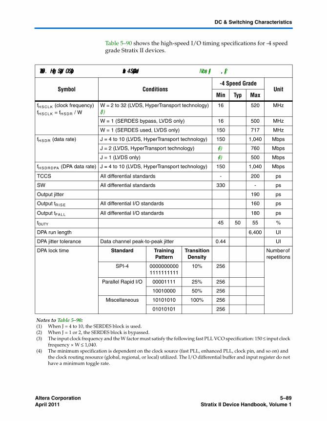
Altera Corporation 5–89April 2011 Stratix II Device Handbook, Volume 1
DC & Switching Characteristics
Table 5–90 shows the high-speed I/O timing specifications for -4 speed grade Stratix II devices.
Table 5–90. High-Speed I/O Specifications for -4 Speed Grade Notes (1), (2)
Symbol Conditions-4 Speed Grade
UnitMin Typ Max
fH S C L K (clock frequency) fH S C L K = fHS D R / W
W = 2 to 32 (LVDS, HyperTransport technology) (3)
16 520 MHz
W = 1 (SERDES bypass, LVDS only) 16 500 MHz
W = 1 (SERDES used, LVDS only) 150 717 MHz
fH S D R (data rate) J = 4 to 10 (LVDS, HyperTransport technology) 150 1,040 Mbps
J = 2 (LVDS, HyperTransport technology) (4) 760 Mbps
J = 1 (LVDS only) (4) 500 Mbps
fH S D R DPA (DPA data rate) J = 4 to 10 (LVDS, HyperTransport technology) 150 1,040 Mbps
TCCS All differential standards - 200 ps
SW All differential standards 330 - ps
Output jitter 190 ps
Output tR I S E All differential I/O standards 160 ps
Output tFA L L All differential I/O standards 180 ps
tDUTY 45 50 55 %
DPA run length 6,400 UI
DPA jitter tolerance Data channel peak-to-peak jitter 0.44 UI
DPA lock time Standard Training Pattern
Transition Density
Number of repetitions
SPI-4 00000000001111111111
10% 256
Parallel Rapid I/O 00001111 25% 256
10010000 50% 256
Miscellaneous 10101010 100% 256
01010101 256
Notes to Table 5–90:(1) When J = 4 to 10, the SERDES block is used.(2) When J = 1 or 2, the SERDES block is bypassed.(3) The input clock frequency and the W factor must satisfy the following fast PLL VCO specification: 150 ≤ input clock
frequency × W ≤ 1,040.(4) The minimum specification is dependent on the clock source (fast PLL, enhanced PLL, clock pin, and so on) and
the clock routing resource (global, regional, or local) utilized. The I/O differential buffer and input register do not have a minimum toggle rate.

5–90 Altera CorporationStratix II Device Handbook, Volume 1 April 2011
High-Speed I/O Specifications
Table 5–91 shows the high-speed I/O timing specifications for -5 speed grade Stratix II devices.
Table 5–91. High-Speed I/O Specifications for -5 Speed Grade Notes (1), (2)
Symbol Conditions-5 Speed Grade
UnitMin Typ Max
fH S C L K (clock frequency) fH S C L K = fHS D R / W
W = 2 to 32 (LVDS, HyperTransport technology) (3)
16 420 MHz
W = 1 (SERDES bypass, LVDS only) 16 500 MHz
W = 1 (SERDES used, LVDS only) 150 640 MHz
fH S D R (data rate) J = 4 to 10 (LVDS, HyperTransport technology) 150 840 Mbps
J = 2 (LVDS, HyperTransport technology) (4) 700 Mbps
J = 1 (LVDS only) (4) 500 Mbps
fH S D R DPA (DPA data rate) J = 4 to 10 (LVDS, HyperTransport technology) 150 840 Mbps
TCCS All differential I/O standards - 200 ps
SW All differential I/O standards 440 - ps
Output jitter 190 ps
Output tR I S E All differential I/O standards 290 ps
Output tFA L L All differential I/O standards 290 ps
tDUTY 45 50 55 %
DPA run length 6,400 UI
DPA jitter tolerance Data channel peak-to-peak jitter 0.44 UI
DPA lock time Standard Training Pattern
Transition Density
Number of repetitions
SPI-4 00000000001111111111
10% 256
Parallel Rapid I/O 00001111 25% 256
10010000 50% 256
Miscellaneous 10101010 100% 256
01010101 256
Notes to Table 5–91:(1) When J = 4 to 10, the SERDES block is used.(2) When J = 1 or 2, the SERDES block is bypassed.(3) The input clock frequency and the W factor must satisfy the following fast PLL VCO specification: 150 ≤ input clock
frequency × W ≤ 1,040.(4) The minimum specification is dependent on the clock source (fast PLL, enhanced PLL, clock pin, and so on) and
the clock routing resource (global, regional, or local) utilized. The I/O differential buffer and input register do not have a minimum toggle rate.

Altera Corporation 5–91April 2011 Stratix II Device Handbook, Volume 1
DC & Switching Characteristics
PLL Timing Specifications
Tables 5–92 and 5–93 describe the Stratix II PLL specifications when operating in both the commercial junction temperature range (0 to 85 °C) and the industrial junction temperature range (–40 to 100 °C).
Table 5–92. Enhanced PLL Specifications (Part 1 of 2)
Name Description Min Typ Max Unit
fI N Input clock frequency 2 500 MHz
fI N P F D Input frequency to the PFD
2 420 MHz
fI N D UT Y Input clock duty cycle 40 60 %
fE I ND U T Y External feedback input clock duty cycle
40 60 %
tI N J I T T E R Input or external feedback clock input jitter tolerance in terms of period jitter.Bandwidth ≤ 0.85 MHz
0.5 ns (p-p)
Input or external feedback clock input jitter tolerance in terms of period jitter.Bandwidth > 0.85 MHz
1.0 ns (p-p)
tO U T J I T T E R Dedicated clock output period jitter
250 ps for ≥ 100 MHz outclk25 mUI for < 100 MHz outclk
ps or mUI (p-p)
tF C O M P External feedback compensation time
10 ns
fO U T Output frequency for internal global or regional clock
1.5 (2)
550.0 MHz
tO U T D UT Y Duty cycle for external clock output (when set to 50%).
45 50 55 %
fS C A N C L K Scanclk frequency 100 MHz
tC O NF I G P L L Time required to reconfigure scan chains for enhanced PLLs
174/fSCANCLK ns
fO U T _ E X T PLL external clock output frequency
1.5 (2)
550.0 (1) MHz
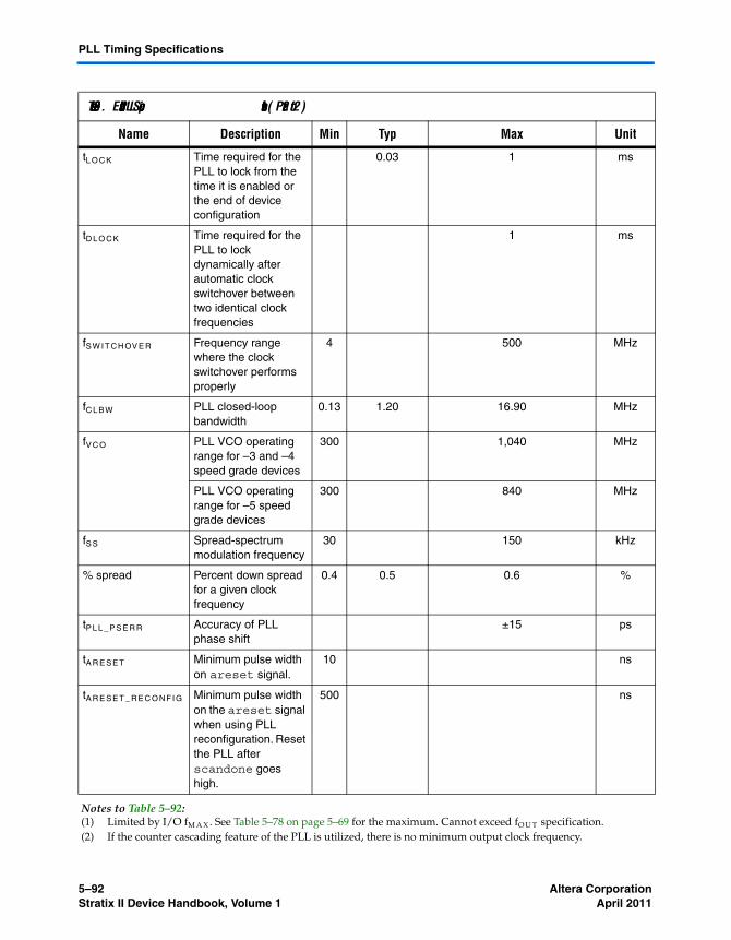
5–92 Altera CorporationStratix II Device Handbook, Volume 1 April 2011
PLL Timing Specifications
tL O C K Time required for the PLL to lock from the time it is enabled or the end of device configuration
0.03 1 ms
tD L O C K Time required for the PLL to lock dynamically after automatic clock switchover between two identical clock frequencies
1 ms
fS W I T CH OV E R Frequency range where the clock switchover performs properly
4 500 MHz
fC L B W PLL closed-loop bandwidth
0.13 1.20 16.90 MHz
fV C O PLL VCO operating range for –3 and –4 speed grade devices
300 1,040 MHz
PLL VCO operating range for –5 speed grade devices
300 840 MHz
fS S Spread-spectrum modulation frequency
30 150 kHz
% spread Percent down spread for a given clock frequency
0.4 0.5 0.6 %
tP L L _ P S E R R Accuracy of PLL phase shift
±15 ps
tA R E S E T Minimum pulse width on areset signal.
10 ns
tA R E S E T _ RE C O NF I G Minimum pulse width on the areset signal when using PLL reconfiguration. Reset the PLL after scandone goes high.
500 ns
Notes to Table 5–92:(1) Limited by I/O fM A X. See Table 5–78 on page 5–69 for the maximum. Cannot exceed fO U T specification.(2) If the counter cascading feature of the PLL is utilized, there is no minimum output clock frequency.
Table 5–92. Enhanced PLL Specifications (Part 2 of 2)
Name Description Min Typ Max Unit
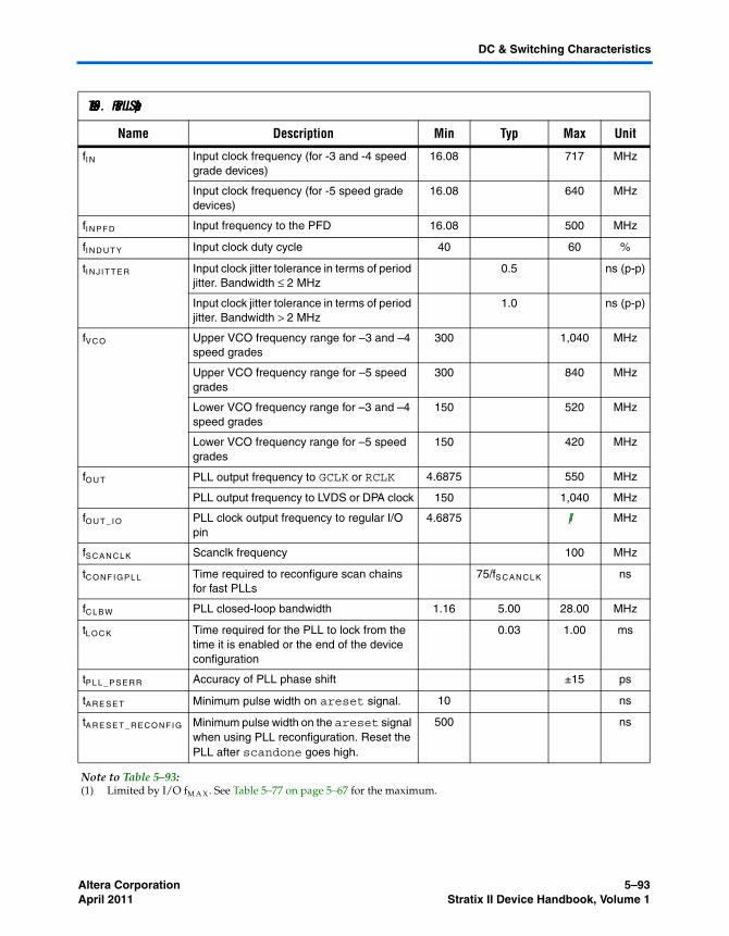
Altera Corporation 5–93April 2011 Stratix II Device Handbook, Volume 1
DC & Switching Characteristics
Table 5–93. Fast PLL Specifications
Name Description Min Typ Max Unit
fI N Input clock frequency (for -3 and -4 speed grade devices)
16.08 717 MHz
Input clock frequency (for -5 speed grade devices)
16.08 640 MHz
fI N P F D Input frequency to the PFD 16.08 500 MHz
fI N D UT Y Input clock duty cycle 40 60 %
tI N J I T T E R Input clock jitter tolerance in terms of period jitter. Bandwidth ≤ 2 MHz
0.5 ns (p-p)
Input clock jitter tolerance in terms of period jitter. Bandwidth > 2 MHz
1.0 ns (p-p)
fV C O Upper VCO frequency range for –3 and –4 speed grades
300 1,040 MHz
Upper VCO frequency range for –5 speed grades
300 840 MHz
Lower VCO frequency range for –3 and –4 speed grades
150 520 MHz
Lower VCO frequency range for –5 speed grades
150 420 MHz
fO U T PLL output frequency to GCLK or RCLK 4.6875 550 MHz
PLL output frequency to LVDS or DPA clock 150 1,040 MHz
fO U T _ I O PLL clock output frequency to regular I/O pin
4.6875 (1) MHz
fS C A N C L K Scanclk frequency 100 MHz
tC O NF I G P L L Time required to reconfigure scan chains for fast PLLs
75/fS CA N CL K ns
fC L B W PLL closed-loop bandwidth 1.16 5.00 28.00 MHz
tL O C K Time required for the PLL to lock from the time it is enabled or the end of the device configuration
0.03 1.00 ms
tP L L _ P S E R R Accuracy of PLL phase shift ±15 ps
tA R E S E T Minimum pulse width on areset signal. 10 ns
tA R E S E T _ RE C O NF I G Minimum pulse width on the areset signal when using PLL reconfiguration. Reset the PLL after scandone goes high.
500 ns
Note to Table 5–93:(1) Limited by I/O fM A X. See Table 5–77 on page 5–67 for the maximum.

5–94 Altera CorporationStratix II Device Handbook, Volume 1 April 2011
External Memory Interface Specifications
External Memory Interface Specifications
Tables 5–94 through 5–101 contain Stratix II device specifications for the dedicated circuitry used for interfacing with external memory devices.
Table 5–95 lists the maximum delay in the fast timing model for the Stratix II DQS delay buffer. Multiply the number of delay buffers that you are using in the DQS logic block to get the maximum delay achievable in your system. For example, if you implement a 90° phase shift at 200 MHz, you use three delay buffers in mode 2. The maximum achievable delay from the DQS block is then 3 × .416 ps = 1.248 ns.
Table 5–94. DLL Frequency Range Specifications
Frequency Mode Frequency Range Resolution (Degrees)
0 100 to 175 30
1 150 to 230 22.5
2 200 to 310 30
3 240 to 400 (–3 speed grade) 36
240 to 350 (–4 and –5 speed grades) 36
Table 5–95. DQS Delay Buffer Maximum Delay in Fast Timing Model
Frequency Mode Maximum Delay Per Delay Buffer (Fast Timing Model) Unit
0 0.833 ns
1, 2, 3 0.416 ns
Table 5–96. DQS Period Jitter Specifications for DLL-Delayed Clock (tDQS_JITTER) Note (1)
Number of DQS Delay Buffer Stages (2) Commercial Industrial Unit
1 80 110 ps
2 110 130 ps
3 130 180 ps
4 160 210 ps
Notes to Table 5–96:(1) Peak-to-peak period jitter on the phase shifted DQS clock.(2) Delay stages used for requested DQS phase shift are reported in your project’s
Compilation Report in the Quartus II software.

Altera Corporation 5–95April 2011 Stratix II Device Handbook, Volume 1
DC & Switching Characteristics
Table 5–97. DQS Phase Jitter Specifications for DLL-Delayed Clock(tDQS PHASE_JITTER) Note (1)
Number of DQS Delay Buffer Stages (2) DQS Phase Jitter Unit
1 30 ps
2 60 ps
3 90 ps
4 120 ps
Notes to Table 5–97:(1) Peak-to-peak phase jitter on the phase shifted DDS clock (digital jitter is caused
by DLL tracking).(2) Delay stages used for requested DQS phase shift are reported in your project’s
Compilation Report in the Quartus II software.
Table 5–98. DQS Phase-Shift Error Specifications for DLL-Delayed Clock (tDQS_PSERR) (1)
Number of DQS Delay Buffer Stages (2) –3 Speed Grade –4 Speed Grade –5 Speed Grade Unit
1 25 30 35 ps
2 50 60 70 ps
3 75 90 105 ps
4 100 120 140 ps
Notes to Table 5–98:(1) This error specification is the absolute maximum and minimum error. For example, skew on three delay buffer
stages in a C3 speed grade is 75 ps or ± 37.5 ps.(2) Delay stages used for requested DQS phase shift are reported in your project’s Compilation Report in the
Quartus II software.
Table 5–99. DQS Bus Clock Skew Adder Specifications (tDQS_CLOCK_SKEW_ADDER)
Mode DQS Clock Skew Adder Unit
×4 DQ per DQS 40 ps
×9 DQ per DQS 70 ps
×18 DQ per DQS 75 ps
×36 DQ per DQS 95 ps
Note to Table 5–99:(1) This skew specification is the absolute maximum and minimum skew. For
example, skew on a ×4 DQ group is 40 ps or ±20 ps.

5–96 Altera CorporationStratix II Device Handbook, Volume 1 April 2011
JTAG Timing Specifications
JTAG Timing Specifications
Figure 5–10 shows the timing requirements for the JTAG signals.
Figure 5–10. Stratix II JTAG Waveforms
Table 5–100. DQS Phase Offset Delay Per Stage Notes (1), (2), (3)
Speed Grade Min Max Unit
-3 9 14 ps
-4 9 14 ps
-5 9 15 ps
Notes to Table 5–100:(1) The delay settings are linear.(2) The valid settings for phase offset are -64 to +63 for frequency mode 0 and -32 to
+31 for frequency modes 1, 2, and 3.(3) The typical value equals the average of the minimum and maximum values.
Table 5–101. DDIO Outputs Half-Period Jitter Notes (1), (2)
Name Description Max Unit
tO U T H A L F J I T T E R Half-period jitter (PLL driving DDIO outputs) 200 ps
Notes to Table 5–101:(1) The worst-case half period is equal to the ideal half period subtracted by the DCD
and half-period jitter values.(2) The half-period jitter was characterized using a PLL driving DDIO outputs.
TDO
TCK
tJPZX tJPCO
tJPH
t JPXZ
tJCP
tJPSU t JCL tJCH
TDI
TMS

Altera Corporation 5–97April 2011 Stratix II Device Handbook, Volume 1
DC & Switching Characteristics
Table 5–102 shows the JTAG timing parameters and values for Stratix II devices.
Document Revision History
Table 5–103 shows the revision history for this chapter.
Table 5–102. Stratix II JTAG Timing Parameters & Values
Symbol Parameter Min Max Unit
tJCP TCK clock period 30 ns
tJCH TCK clock high time 13 ns
tJCL TCK clock low time 13 ns
tJPSU JTAG port setup time 3 ns
tJPH JTAG port hold time 5 ns
tJPCO JTAG port clock to output 11 (1) ns
tJPZX JTAG port high impedance to valid output 14 (1) ns
tJPXZ JTAG port valid output to high impedance 14 (1) ns
Note to Table 5–102:(1) A 1 ns adder is required for each VC C I O voltage step down from 3.3 V. For
example, tJPCO = 12 ns if VC C I O of the TDO I/O bank = 2.5 V, or 13 ns if it equals 1.8 V.
Table 5–103. Document Revision History (Part 1 of 3)
Date and Document
VersionChanges Made Summary of Changes
April 2011, v4.5 Updated Table 5–3. Added operating junction temperature for military use.
July 2009, v4.4 Updated Table 5–92. Updated the spread spectrum modulation frequency (fS S) from (100 kHz–500 kHz) to (30 kHz–150 kHz).
May 2007, v4.3 ● Updated RCONF in Table 5–4.● Updated fIN (min) in Table 5–92.● Updated fIN and fINPFD in Table 5–93.
—
Moved the Document Revision History section to the end of the chapter.
—
5–98 Altera CorporationStratix II Device Handbook, Volume 1 April 2011
Document Revision History
August, 2006, v4.2
Updated Table 5–73, Table 5–75, Table 5–77, Table 5–78, Table 5–79, Table 5–81, Table 5–85, and Table 5–87.
—
April 2006, v4.1 ● Updated Table 5–3.● Updated Table 5–11.● Updated Figures 5–8 and 5–9.● Added parallel on-chip termination information to
“On-Chip Termination Specifications” section.● Updated Tables 5–28, 5–30,5–31, and 5–34.● Updated Table 5–78, Tables 5–81 through 5–90,
and Tables 5–92, 5–93, and 5–98.● Updated “PLL Timing Specifications” section.● Updated “External Memory Interface
Specifications” section.● Added Tables 5–95 and 5–101.● Updated “JTAG Timing Specifications” section,
including Figure 5–10 and Table 5–102.
● Changed 0.2 MHz to 2 MHz in Table 5–93.
● Added new spec for half period jitter (Table 5–101).
● Added support for PLL clock switchover for industrial temperature range.
● Changed fI N P F D (min) spec from 4 MHz to 2 MHz in Table 5–92.
● Fixed typo in tO UT J I T T E R specification in Table 5–92.
● Updated VDI F AC & DC max specifications in Table 5–28.
● Updated minimum values for tJ C H, tJ C L, and tJ P S U in Table 5–102.
● Update maximum values for tJ P CO, tJ P Z X, and tJ P X Z in Table 5–102.
December 2005, v4.0
● Updated “External Memory Interface Specifications” section.
● Updated timing numbers throughout chapter.
—
July 2005, v3.1 ● Updated HyperTransport technology information in Table 5–13.
● Updated “Timing Model” section.● Updated “PLL Timing Specifications” section.● Updated “External Memory Interface
Specifications” section.
—
May 2005, v3.0 ● Updated tables throughout chapter.● Updated “Power Consumption” section.● Added various tables.● Replaced “Maximum Input & Output Clock Rate”
section with “Maximum Input & Output Clock Toggle Rate” section.
● Added “Duty Cycle Distortion” section.● Added “External Memory Interface Specifications”
section.
—
March 2005, v2.2
Updated tables in “Internal Timing Parameters” section.
—
January 2005, v2.1
Updated input rise and fall time. —
Table 5–103. Document Revision History (Part 2 of 3)
Date and Document
VersionChanges Made Summary of Changes
Altera Corporation 5–99April 2011 Stratix II Device Handbook, Volume 1
DC & Switching Characteristics
January 2005, v2.0
● Updated the “Power Consumption” section.● Added the “High-Speed I/O Specifications” and
“On-Chip Termination Specifications” sections.● Removed the ESD Protection Specifications
section.● Updated Tables 5–3 through 5–13, 5–16 through
5–18, 5–21, 5–35, 5–39, and 5–40.● Updated tables in “Timing Model” section.● Added Tables 5–30 and 5–31.
—
October 2004, v1.2
● Updated Table 5–3.● Updated introduction text in the “PLL Timing
Specifications” section.
—
July 2004, v1.1 ● Re-organized chapter.● Added typical values and CO U T F B to Table 5–32.● Added undershoot specification to Note (4) for
Tables 5–1 through 5–9.● Added Note (1) to Tables 5–5 and 5–6.● Added VI D and VI CM to Table 5–10.● Added “I/O Timing Measurement Methodology”
section.● Added Table 5–72.● Updated Tables 5–1 through 5–2 and Tables 5–24
through 5–29.
—
February 2004, v1.0
Added document to the Stratix II Device Handbook. —
Table 5–103. Document Revision History (Part 3 of 3)
Date and Document
VersionChanges Made Summary of Changes

5–100 Altera CorporationStratix II Device Handbook, Volume 1 April 2011
Document Revision History