advanced methodology of nano device analysis - sematech
TRANSCRIPT

PAGE 1PAGE Sematech 2012
Advanced Methodology of Advanced Methodology of NanoNano Device AnalysisDevice Analysis-- Characterization and identification of Characterization and identification of nanonano defects in ICs, TSV, LED, and defects in ICs, TSV, LED, and
CMP slurry CMP slurry
Yong-Fen Hsieh, CEO of MA-tek
Contributors include JS Bow, CA Lu, YF Ko, and Kari n Ho.
Nanodefects session

PAGE 2PAGE Proprietary, DO NOT COPY WITHOUT PERMISSION. Any page, or pages of this report can not be used separately.
Agenda
Major applications will cover the topics as follows .• Untra-thin dielectrics:
– Thickness and Composition Characterization of High-K and ONO
• De-convolution of overlapped peaks of Si/Ta/Hf– TEM/EDX Line Profile
• As doping in S/D region– Short acquisition time with overlapped peaks de-convolution by Q-
map processing
• Si-Ge quantitative analysis– PMOS/NMOS identification by P-V EDX mapping– Ge% determination (EDX vs. SIMS)– Defects characterization
• Characterization of Recessed Gate – non-uniform gate oxide growth
• Device Burn-out at Spacer Edge – LDD junction breakdown
• Fault Isolation of a TSV Array by InGaAs Analysis• Blue LED, AlGaN/InGaN Quantum Well, Characterization
– Comparison of SIMS Depth Profile vs. TEM/EDX Line Scan
• Study of CMP slurry by Frozen Method and Nano Pipet
Metal-1 (Cu)
Metal-4 (Cul)
gate
Metal-2 (Cu)
Contact (W-plug)
Metal-3 (Cu)
This talk will focus mainly on P-V and X-S TEM 3D E DX, where EELS, SIMS, RBS, SEM, FIB will be employed for comparison.

PAGE 3PAGE Proprietary, DO NOT COPY WITHOUT PERMISSION. Any page, or pages of this report can not be used separately.
Recent Progress of Analytical Tools DevelopmentRecent Progress of Analytical Tools Development
• TEM/EDX 3D detectors : FEI Osiris
• Various Softwares for data processing : Bruker, Q-map, TIA, self-developed
TEM/EDX
Easy operation
Insensitive to light elementssuch as C, N, O, and F.
SIMSTEM/EELS
Crater of 100 um scale range,Special designed pattern is required.
Complicated operation &thin TEM sample is required.
Poor detection limit
This combination is realized now.This combination is realized now.
> 0.1%
<1ppm
Z >8
Z <29
PAGE 4PAGE Proprietary, DO NOT COPY WITHOUT PERMISSION. Any page, or pages of this report can not be used separately.
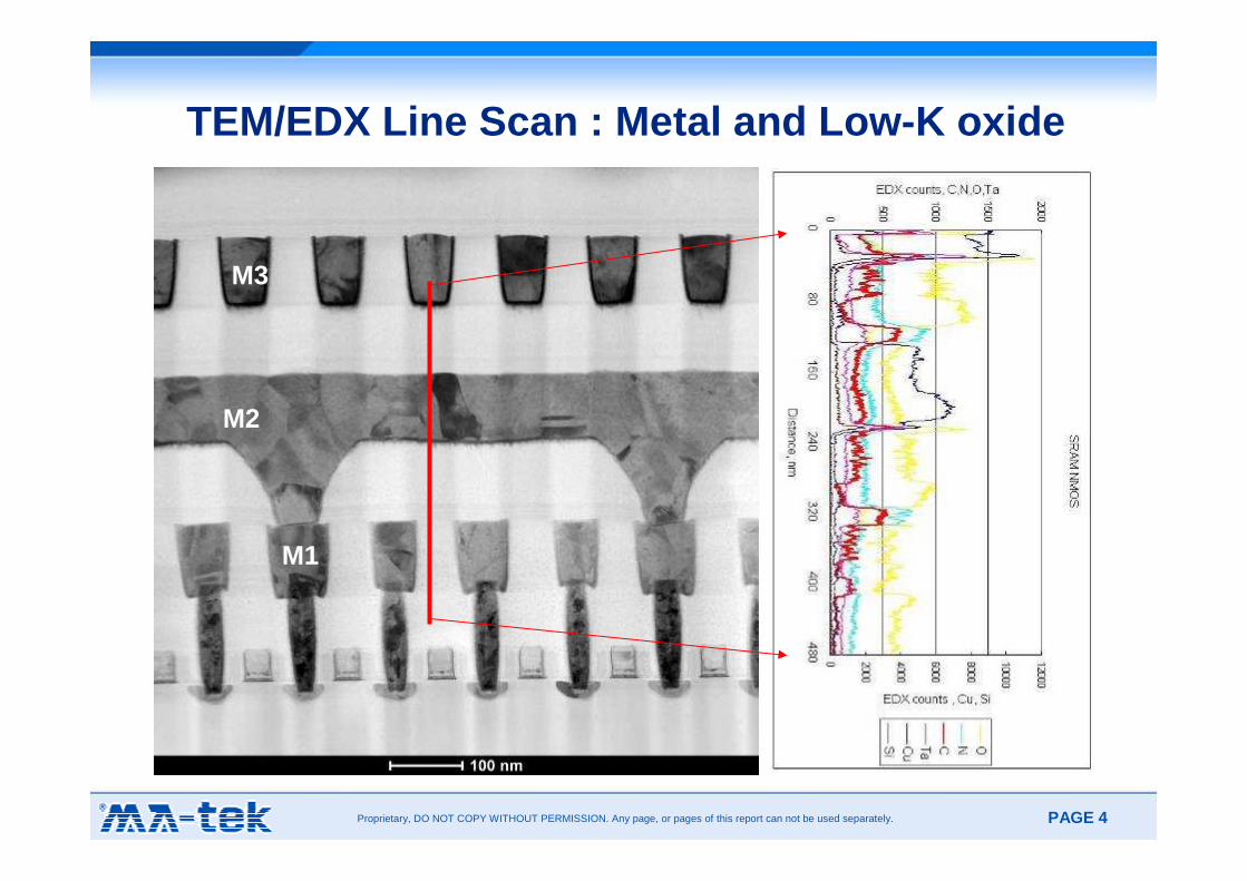
TEM/EDX Line Scan : Metal and Low -K oxide
M1
M2
M3

PAGE 5PAGE Proprietary, DO NOT COPY WITHOUT PERMISSION. Any page, or pages of this report can not be used separately.
SRAM NMOS
0
500
1000
1500
2000
0 80 160 240 320 400 480
Distance, nm
ED
X c
ount
s, C
,N,O
,Ta
0
2000
4000
6000
8000
10000
12000
ED
X c
ount
s , C
u, S
i
O
N
C
Ta
Cu
Si
Continue – TEM/EDX Line-scanning : Metal and Low -K
Via
2 et
chin
g st
op la
yer.
Via
1 et
chin
g st
op la
yer.
M1
tren
ch e
tchi
ng s
top
laye
r.
M2 IMD-1M3M1
TRENCHIMD-2 ILD
PAGE 6PAGE Proprietary, DO NOT COPY WITHOUT PERMISSION. Any page, or pages of this report can not be used separately.
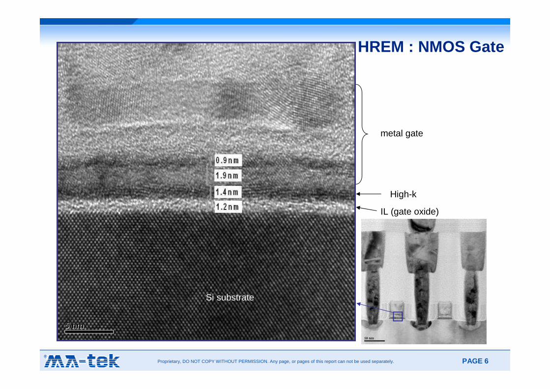
IL (gate oxide)
High-k
metal gate
Si substrate
HREM : NMOS Gate

PAGE 7PAGE Proprietary, DO NOT COPY WITHOUT PERMISSION. Any page, or pages of this report can not be used separately.
TEM/EDX Line Scan : NMOS Gate

PAGE 8PAGE Proprietary, DO NOT COPY WITHOUT PERMISSION. Any page, or pages of this report can not be used separately.
0
10
20
30
40
50
60
70
80
0 6 12 18 24 30 36 42 48 54 60 66
Distance , nm
ED
X c
ount
s
O
Si
Ti
N
Ta
Al
Hf
Continue – TEM/EDX Line Scan : NMOS Gate
IL (
Gat
e O
xide
)H
fbas
ed H
igh-
kT
iN
Ta-
Si
Ti-A
l-O
TiNTi-Al Ti-r
ich
Ti-A
l
Ti-Al-OSi
substrateSi-oxide

PAGE 9PAGE Proprietary, DO NOT COPY WITHOUT PERMISSION. Any page, or pages of this report can not be used separately.
Page Page 99
TEM BF(43 kx)
ONO Elemental Mapping by TEM / ONO Elemental Mapping by TEM / EELS EELS
-- Flash Memory CellsFlash Memory Cells
The thickness of poly-Si-2 is measured to be 42nm.
The thickness of poly-Si-1 is measured to be 39.1nm
ONO thicknesses are measured to be 5.8/2.9/4.6 nm
by HREM respectively.

PAGE 10PAGE Proprietary, DO NOT COPY WITHOUT PERMISSION. Any page, or pages of this report can not be used separately.
Page Page 1010
ONO Elemental Mapping by TEM / EELS
- Flash Memory Cells
Zero Loss Image Nitrogen map
Silicon map Oxygen map
EELS was chosen for ONO elemental mapping, owing to:
(1) Conventional EDX analysis has to tilt certain angle, because the lamella is not “edge-on” toward EDX detector.
(2) The X-ray radiation efficiency of light elements, such as C, N and O, are that good as that of heavy elements.

PAGE 11PAGE Proprietary, DO NOT COPY WITHOUT PERMISSION. Any page, or pages of this report can not be used separately.
Zero Loss Image
Si
N O
EELS Mapping – Nitrogen, Oxygen
By Tencai G2 F20
Mapping time ~ 1 min per element, but TEM/EELS system alignment and operation parameters settingtake long time of operation (2-3hrs). Sample drifting shall be an issue of EELS analysis.
In addition, thin sample, < 50nm, is required, which is critical to EELS signal enhancement.

PAGE 12PAGE Proprietary, DO NOT COPY WITHOUT PERMISSION. Any page, or pages of this report can not be used separately.
HAADF
Si
N O
Mapping time = 30mins
By FEI Osiris,equipped with 3D EDX, 4 detectors
3D EDX Mapping – Nitrogen, Oxygen
This is the same sample for EELS mapping, ~50nm thick.
If a thicker specimen (~100nm) is used, the intensity will be even higher.

PAGE 13PAGE Proprietary, DO NOT COPY WITHOUT PERMISSION. Any page, or pages of this report can not be used separately.
0
20
40
60
80
100
120
0 0.002 0.004 0.006 0.008 0.01 0.012 0.014 0.016
Si ON
EDX Line profile extracted from 3D EDX mapping data
5.1nm
6.8nm5.1nm
O
Typically, people use FWHM to derive layer thickness, but there is certain deviation from HREM measurement.
Cou
nts,
arb
itrar
y un
it

PAGE 14PAGE Proprietary, DO NOT COPY WITHOUT PERMISSION. Any page, or pages of this report can not be used separately.
0
20
40
60
80
100
12 14 16 18 20 22 24 26 28 30 32
Distance (nm)
at%
N O Si
Consistent N & O depth profiling by 3D EDX & EELS in S iOxNy Layer
0.00E+00
1.00E+05
2.00E+05
3.00E+05
4.00E+05
5.00E+05
0 2 4 6 8 10 12 14 16 18 20
Distance (nm)
Inte
nsity
N ON
Pt SiO2 SiOxNySi
SiO2
EDX
EELS
0
20
40
60
80
100
0 5 10 15 20 25 30 35
Distance (nm)
at%
N O Si
N O
OSi
3D EDX EELS
O
O

PAGE 15PAGE Proprietary, DO NOT COPY WITHOUT PERMISSION. Any page, or pages of this report can not be used separately.
0.0
20.0
40.0
60.0
80.0
100.0
0.0 5.0 10.0 15.0 20.0 25.0 30.0 35.0Position (nm)
at%
N O SiN O Si
SiOxNy SiOxSiOxPt Si
���� The deviation of N and O in three line profiles is within 5%.���� The large deviation in Pt layers was resulted from its complicated atomic structure.
Repeatability of 3D EDX Line Profiles
PAGE 16PAGE Proprietary, DO NOT COPY WITHOUT PERMISSION. Any page, or pages of this report can not be used separately.
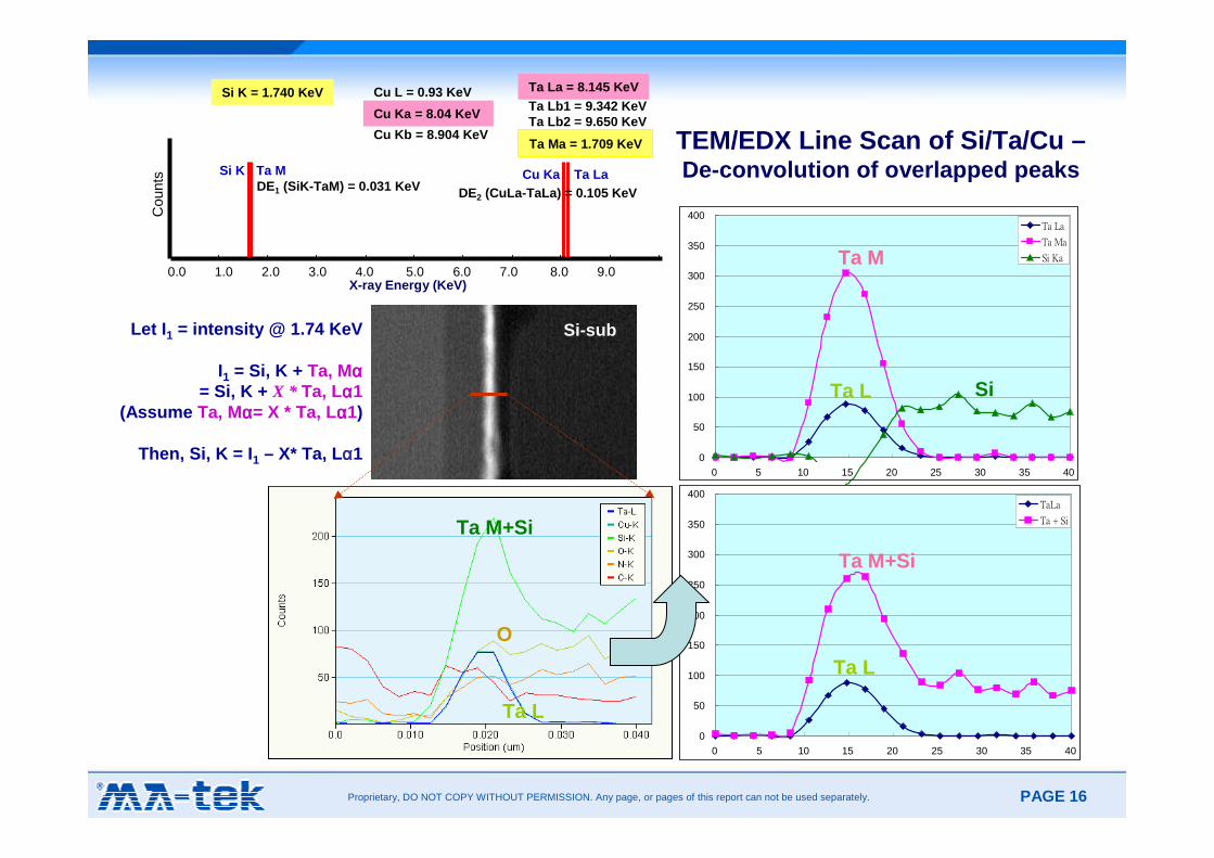
Ta M+Si
Ta L
O
Si-sub
TEM/EDX Line Scan of Si/Ta/Cu –De-convolution of overlapped peaks
0
50
100
150
200
250
300
350
400
0 5 10 15 20 25 30 35 40
Ta La
Ta Ma
Si Ka
0
50
100
150
200
250
300
350
400
0 5 10 15 20 25 30 35 40
TaLa
Ta + Si
Ta M
Si
Ta L
Ta L
Ta M+Si
Si K Cu Ka
0.0 1.0 2.0 3.0 4.0 5.0 6.0 7.0 8.0 9.0X-ray Energy (KeV)
Cou
nts
Si K = 1.740 KeV Cu L = 0.93 KeV Ta La = 8.145 KeV
Ta LaTa MDE1 (SiK-TaM) = 0.031 KeV DE2 (CuLa-TaLa) = 0.105 KeV
Ta Lb1 = 9.342 KeVTa Lb2 = 9.650 KeV
Ta Ma = 1.709 KeV
Cu Ka = 8.04 KeV
Cu Kb = 8.904 KeV
Let I 1 = intensity @ 1.74 KeV
I1 = Si, K + Ta, Mα α α α = Si, K + X * Ta, Lαααα1
(Assume Ta, Mαααα= X * Ta, Lαααα1)
Then, Si, K = I 1 – X* Ta, Lαααα1
PAGE 17PAGE Proprietary, DO NOT COPY WITHOUT PERMISSION. Any page, or pages of this report can not be used separately.
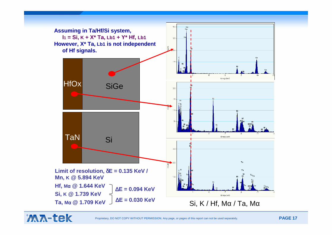
Si, K / Hf, Mα / Ta, MαSi, K @ 1.739 KeVHf, Mαααα @ 1.644 KeV
Ta, Mα α α α @ 1.709 KeV
∆∆∆∆E = 0.094 KeV
∆∆∆∆E = 0.030 KeV
Limit of resolution, δδδδE = 0.135 KeV / Mn, K @ 5.894 KeV
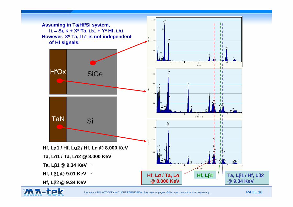
SiGeHfOx
SiTaN
Assuming in Ta/Hf/Si system,I1 = Si, K + X* Ta, Lb1 + Y* Hf, Lb1
However, X* Ta, Lb1 is not independent of Hf signals.
PAGE 18PAGE Proprietary, DO NOT COPY WITHOUT PERMISSION. Any page, or pages of this report can not be used separately.
SiGeHfOx
SiTaN
Hf, Lαααα1 / Hf, Lαααα2 / Hf, Ln @ 8.000 KeV
Ta, Lαααα1 / Ta, Lαααα2 @ 8.000 KeV
Hf, Lα α α α / Ta, Lαααα@ 8.000 KeV
Hf, Lβ1β1β1β1 Ta, Lβ1 / β1 / β1 / β1 / Hf, Lβ2β2β2β2@ 9.34 KeVHf, Lβ2 β2 β2 β2 @ 9.34 KeV
Ta, Lβ1 β1 β1 β1 @ 9.34 KeV
Hf, Lβ1 β1 β1 β1 @ 9.01 KeV
Assuming in Ta/Hf/Si system,I1 = Si, K + X* Ta, Lb1 + Y* Hf, Lb1
However, X* Ta, Lb1 is not independent of Hf signals.

PAGE 19PAGE Proprietary, DO NOT COPY WITHOUT PERMISSION. Any page, or pages of this report can not be used separately.
0
1000
2000
3000
4000
5000
6000
0 5 10 15 20 25 30 35 40 45 50
Position (nm)
Inte
nsity
Hf-Lb Ta-Lb Ti-K Si-K Ge-L O-K
Original Original EDX line profiles. Low intensity line profiles of Ta, Lβ1
and Hf, Lβ1 lie below Si line profile (red line).
SiGe
HfOx HfOx
TaN TaN
TiN TiN

PAGE 20PAGE Proprietary, DO NOT COPY WITHOUT PERMISSION. Any page, or pages of this report can not be used separately.
0
1000
2000
3000
4000
5000
6000
0 5 10 15 20 25 30 35 40 45 50
Position (nm)
Inte
nsity
Hf M Ta M Ti K Si K Ge L O K
Si >> Ta/Hf.
(YHf = 3.6; XTa = 5.35)
This is an ideal result, which needs semi-empirical adjustment by engineering efforts.It is easy to separate Si from Hf (or Ta) in single stacked layer.It becomes much more complicated, when both Hf and Ta are involved.
ProcessedProcessed EDX line profiles. High intensity and separate line profiles of Ta Lβ1
(blue line) and Hf Lβ1 (purple line), but Si, K line profile became to be too low.
SiGe
HfOx HfOx
TaN TaN
TiN TiN
Si-rich Si-rich

PAGE 21PAGE Proprietary, DO NOT COPY WITHOUT PERMISSION. Any page, or pages of this report can not be used separately.
STEM Image W As N
Ni O Si Ti
TEM/EDX Mapping TEM/EDX Mapping –– As doping in S/D regionAs doping in S/D region
Acquisition 10 mins without Q-Map data processing- Artifacts was resulted from peaks overlap (As, W, and Si).
Prior Art of EDX Mapping, under typical operation conditions, it takes ~ 30 mins for a set of EDX maps. However, As doping profile in S/D region will be only available when acquisition time is more than 4 hrs . Data below were acquired by FEI Osiris, equipped with 3D EDX detectors.

PAGE 22PAGE Proprietary, DO NOT COPY WITHOUT PERMISSION. Any page, or pages of this report can not be used separately.
STEM Image W As N
Ni O Si Ti
Acquisition 10 mins and Q-Map data processing (2 hrs )- FREE of artifacts
Prior Art of EDX Mapping, under typical operation conditions, it takes ~ 30 mins for a set of EDX maps. However, As doping profile in S/D region will be only available when acquisition time is more than 4 hrs . Data below were acquired by FEI Osiris, equipped with 3D EDX detectors.
TEM/EDX Mapping TEM/EDX Mapping –– As doping in S/D regionAs doping in S/D region

PAGE 23PAGE Proprietary, DO NOT COPY WITHOUT PERMISSION. Any page, or pages of this report can not be used separately.
TEM BF
HAADF (ZC)
Identification of PMOS device layout - Comparison of TEM and HAADF(ZC)
The unit cell was marked by red rectangles.HAADF imaging of NMOS/PMOS interface can define the cell size better than TEM imaging.
NMOS / PMOS / NMOS

PAGE 24PAGE Proprietary, DO NOT COPY WITHOUT PERMISSION. Any page, or pages of this report can not be used separately.
Page Page 2424
NMOS/PMOSinterface
The interface of NMOS poly and PMOS poly indicated that the processes of the NMOS poly and PMOS poly needed two masks.
Plain View (PV) TEM 43kx
NMOS active area
PMOS active area
NMOS poly
PMOS poly
contact

PAGE 25PAGE Proprietary, DO NOT COPY WITHOUT PERMISSION. Any page, or pages of this report can not be used separately.
Mapping : NMOS/PMOS Differentiation
The NMOS active area was marked by purple rectangles, and discontinuous PMOS active
area was marked by blue rectangles. The elemental maps of Al, Ta and Ge were
shown clearly in NMOS and PMOS. Obviously, PV-TEM sample thickness is estimated to be
> 200nm in this study.
This work can be applied to benchmark analysis and IP infringement case.
GeTa (HK metal P-gate)
Al
NMOS
PMOS

PAGE 26PAGE Proprietary, DO NOT COPY WITHOUT PERMISSION. Any page, or pages of this report can not be used separately.
Page Page 2626
Ge (Si-Ge) N
HfNi (metal silicides)Ta (HK metal P-gate)W (contact)
C Si Al (HK metal P/N-gate) Ti (HK metal P/N-gate)
TEM/EDX Elemental Mapping
Raw Data
PMOS
PMOS
PMOS

PAGE 27PAGE Proprietary, DO NOT COPY WITHOUT PERMISSION. Any page, or pages of this report can not be used separately.
SIMS Depth Profiling of 40% graded Ge and 26% Ge Characterized by a calibration standards prepared b y EAG.
0
5
10
15
20
25
30
35
40
45
50
0 20 40 60 80 100 120 140
Depth:[nm]
Con
cent
ratio
n:[A
tom
ic%
]
Ge(#1)
Ge(#5)Ge(#1)Ge(#1)Ge(#1)Ge(#1)
Ge(#5)Ge(#5)Ge(#5)Ge(#5)
40% graded Ge
26% Ge
� Quantitative analysis by TEM/EELS is much more comp licated than that by TEM/EDX.
- The specimen thickness has to be thinner than 50 nm to ensure single scattering condition, which is a must for EELS quantitative analysis. This will be challenging in TEM sample preparation.
- The acquisition time for Si and Ge will be quite different, because of the large energy loss difference of the corresponding characteristic edges (Si L2,3 @ 99 eV; Ge L2,3 @ 1217 eV). This will result in extra errors in quantitative analysis.
Si-Ge
Si

PAGE 28PAGE Proprietary, DO NOT COPY WITHOUT PERMISSION. Any page, or pages of this report can not be used separately.
� There are 6 data points for TEM/EDX at each positio n, 3 from t = 80 nm (hollow marks), and 3 from t = 120 nm (solid marks). Thickness effect is not obvious.
� The concentration of Ge of both 26% and ~40% are ve ry well consistent with those analyzed by SIMS, 1-2% off-set only, where Si, Ge, and oxygen concentrations are obtained from EDX signal intensi ty.
t = 80/120 nm
0
20
40
60
0 1 2 3 4
Position
(at%
)
SIMS TEM/EDX
26% Ge
~ 40% Ge
Comparison of TEM/EDX and SIMS
(Oxygen included)

PAGE 29PAGE Proprietary, DO NOT COPY WITHOUT PERMISSION. Any page, or pages of this report can not be used separately.
� There are 6 data points for TEM/EDX at each positio n, 3 from t = 80 nm (hollow marks), and 3 from t = 120 nm (solid marks). Thickness effect of TEM sample is not obvious.
� The concentration of Ge obtained from TEM/EDX are 3 - 6% off-set from those of SIMS, if Si-Ge are recalculated with oxygen excluded .
t = 80/120 nm
0
20
40
60
0 1 2 3 4Position
Ge/
Si r
atio
n
26% Ge
~ 40% Ge
SIMS TEM/EDX
Comparison of TEM/EDX and SIMS
(Oxygen excluded)

PAGE 30PAGE Proprietary, DO NOT COPY WITHOUT PERMISSION. Any page, or pages of this report can not be used separately.
0.0
20.0
40.0
60.0
80.0
100.0
20.0 60.0 100.0 140.0Distance (nm)
at%
%Si %Ge %O
Quantitative Analysis of Si-Ge by TEM/EDX (2)
~ 30
���� The line profile was performed on a QMap processed i mage.
���� The Ge concentration is measured to be ~ 30% throug h the film.
���� The deviation is about 4% compared with RBS data.

PAGE 31PAGE Proprietary, DO NOT COPY WITHOUT PERMISSION. Any page, or pages of this report can not be used separately.
Plan-view and Cross-section TEM reveals lateral, fa cet growth in different directions.
interface defects
SiGe
SiO2
SiSi-Ge Overgrowth on STI oxide is dependent on crysta l orientation . The degree of overgrowth and defect density can be studied in terms of Pattern/Size Effects and Material Growth conditions.

PAGE 32PAGE Proprietary, DO NOT COPY WITHOUT PERMISSION. Any page, or pages of this report can not be used separately.
TEM Top view (PlanTEM Top view (Plan --view)view)
Discontinuous Si-Ge islands
FIB Top view (PlanFIB Top view (Plan --view)view)
Discontinuous Si-Ge islands

PAGE 33PAGE Proprietary, DO NOT COPY WITHOUT PERMISSION. Any page, or pages of this report can not be used separately.
1um
0.79um
512Mb DDR SDRAM512Mb DDR SDRAM–– Recessed Gate (nonRecessed Gate (non --uniform gate oxide growth)uniform gate oxide growth)
P-2, local inter-connect, BL
P-1, gate, WL
BLC NCNC
RGRG RGRG

PAGE 34PAGE Proprietary, DO NOT COPY WITHOUT PERMISSION. Any page, or pages of this report can not be used separately.
DRAM cell arrayDRAM cell array --
Characterization of Characterization of gate oxide thinning gate oxide thinning
by planby plan --view TEMview TEM
Cross-section
A A’
Bit line contact
Channel
Gate Oxide Thinning at Trench Corner
Bare Si sub.
Poly-Si gate on Si sub.
X-S
P-V
BLC NCNC
BLC NCNC
BLC
NC
WL
WL
Recessed GateRecessed Gate
RGRG RGRG

PAGE 35PAGE Proprietary, DO NOT COPY WITHOUT PERMISSION. Any page, or pages of this report can not be used separately.
Page Page 3535
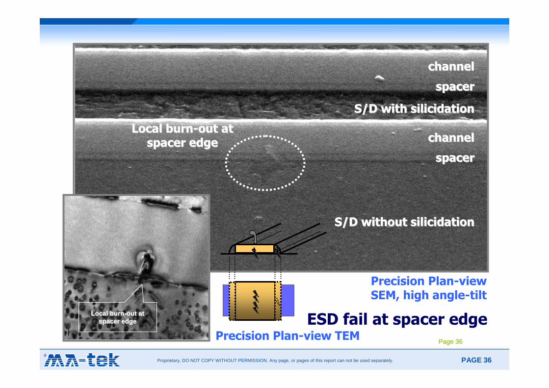
TEM imageTEM image
Failure site
S/D implantation
Channel region
Channel region
Silicide S/DSEM imageSEM image
Device BurnDevice Burn --out at Spacer Edge out at Spacer Edge –– LDD junction breakdownLDD junction breakdown(The burn(The burn --out mark is visible in TEM, but invisible in SEM )out mark is visible in TEM, but invisible in SEM )
PAGE 36PAGE Proprietary, DO NOT COPY WITHOUT PERMISSION. Any page, or pages of this report can not be used separately.
channelchannel
channelchannel
S/D with S/D with silicidationsilicidation
S/D without S/D without silicidationsilicidation
spacerspacer
spacerspacer
Local burnLocal burn--out at out at
spacer edgespacer edge
Precision Plan-view SEM, high angle-tilt
Page Page 3636
Local burnLocal burn --out at out at spacer edgespacer edge
Precision Plan-view TEM
ESD fail at spacer edge

PAGE 37PAGE Proprietary, DO NOT COPY WITHOUT PERMISSION. Any page, or pages of this report can not be used separately.
FIB X-S
TSV
Laser mark
Si
Fault Isolation of Fault Isolation of a TSV Array a TSV Array
by by InGaAsInGaAs AAnalysisnalysis X-S SEM
emission spot
P-V OM in InGaAs
OXIDE
TSV (Au)
Si
Gold metal fill in oxide crack and penetrate to silicon substrate
Step1
Step2
Step3
Step4
Deep trench > 30 um
X-S OM in InGaAs

PAGE 38PAGE Proprietary, DO NOT COPY WITHOUT PERMISSION. Any page, or pages of this report can not be used separately.
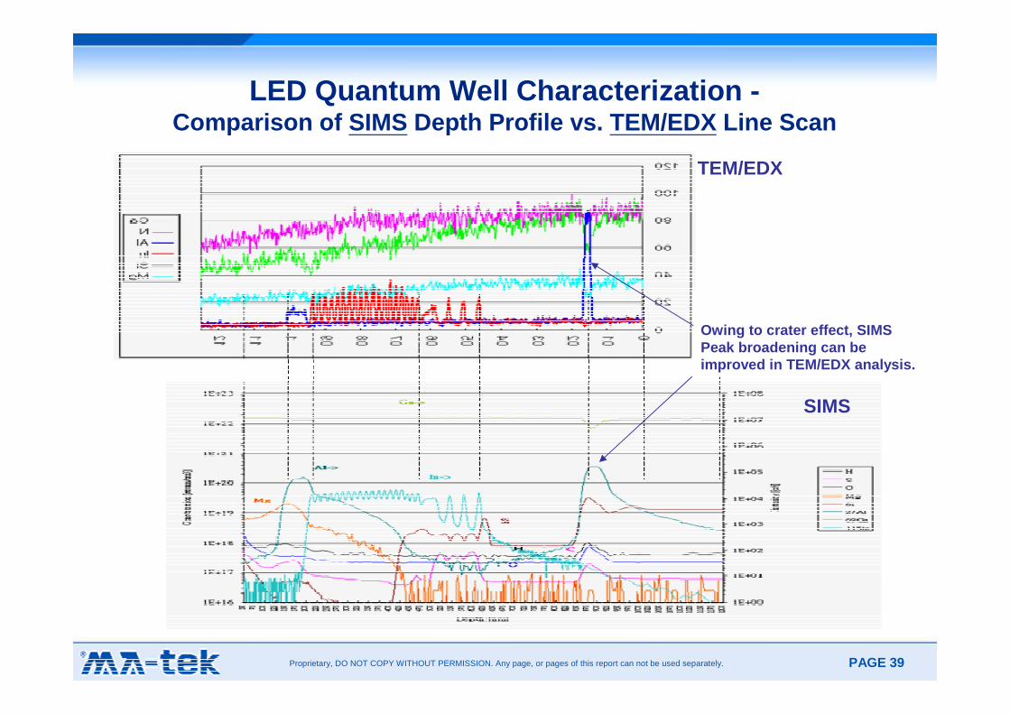
LED AlGaN/InGaN Quantum Well Characterization -Comparison of SIMS Depth Profile vs. TEM/EDX Line Scan
Difficulties of SIMS analysis:1. Deep crater > 8um2. Surface roughness resulted from faceted
epitaxial layer
PAGE 39PAGE Proprietary, DO NOT COPY WITHOUT PERMISSION. Any page, or pages of this report can not be used separately.
LED Quantum Well Characterization -Comparison of SIMS Depth Profile vs. TEM/EDX Line Scan
SIMS
Owing to crater effect, SIMS Peak broadening can be improved in TEM/EDX analysis.
TEM/EDX

PAGE 40PAGE Proprietary, DO NOT COPY WITHOUT PERMISSION. Any page, or pages of this report can not be used separately.
Depth Profiling of Al and In in Thick layer vs. Thin layer
SIMS: Al peak broadening owing to sidewall effect in deep crater.

PAGE 41PAGE Proprietary, DO NOT COPY WITHOUT PERMISSION. Any page, or pages of this report can not be used separately.
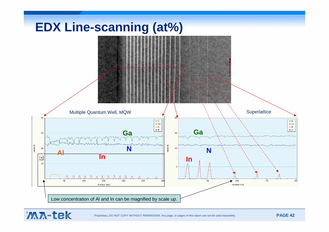
N In
EDX Mapping
HAADF Image
In Al
N Ga
N is homogeneous through the area analyzed.
Addition of In or Al seems to replace Ga atoms in the GaN.
PAGE 42PAGE Proprietary, DO NOT COPY WITHOUT PERMISSION. Any page, or pages of this report can not be used separately.
EDX Line -scanning (at%)
Ga Ga
N NIn In
Al
Multiple Quantum Well, MQW Superlattice
Low concentration of Al and In can be magnified by scale up.

PAGE 43PAGE Proprietary, DO NOT COPY WITHOUT PERMISSION. Any page, or pages of this report can not be used separately.
TEM for abrasive analysis – Sample preparation methods
Aggregation status
Cryo-TEM
Nanopipet /TEM
Copper grid: aggregated in drying processes
Native status in solution
Size200 nm100 nm50 nm 500 nm
OM
PrimaryparticleCharacterization
request SecondaryParticle
Unwanted aggregates or big particles
Size & Morphology & Concentration
Wafer defects
CMP performance

PAGE 44PAGE Proprietary, DO NOT COPY WITHOUT PERMISSION. Any page, or pages of this report can not be used separately.
[Frozen Liquid] Cryo -TEM – Direct Image
Holey carbon support film
Scale bar: 20 nm
12
43

PAGE 45PAGE Proprietary, DO NOT COPY WITHOUT PERMISSION. Any page, or pages of this report can not be used separately.
Particle size distribution
0 20 40 60 80 100 120 1400
5
10
15
20
Par
ticle
num
ber
%
dA (nm)
All particles Circularity < 0.8 Circularity > 0.8
Particle-2
Particle-2 Cluster
* dA = (4A/π)1/2, total calculated n = 1044
53.4 ± 9.9 nm(n = 625)
72.2 ± 16.9 nm (n = 419)
0
10
20
30
40
50
60
Particle-2 Particle -2 Cluster
part
icle
num
ber
(%)
0.2 0.4 0.6 0.8 1.00
2
4
6
8
10
12
Par
ticle
num
ber
%
Circularity
Particle-2 Cluster
Particle-2
20 40 60 80 100 1200.2
0.4
0.6
0.8
1.0
dA (nm)
Circ
ular
ity
Primary particle-2
Circularity = 4ππππ* Area
(Perimeter) 2

PAGE 46PAGE Proprietary, DO NOT COPY WITHOUT PERMISSION. Any page, or pages of this report can not be used separately.
Direct Image of Live Liquid in TEM / Direct Image of Live Liquid in TEM / NanopipetNanopipet[K[K --Kit]Kit]
Window and gap of the nanopipet is ~5um, which can b e tailored per research interest.
Scale bar: 100 nm

PAGE 47PAGE Proprietary, DO NOT COPY WITHOUT PERMISSION. Any page, or pages of this report can not be used separately.
Comparison, Comparison, CryoCryo --TEM vs. TEM vs. NanopipetNanopipet TEMTEM
0 20 40 60 80 100 120 1400
30
60
90
120
150 Cryo-TEM Nanopipet / TEM
Cou
nted
par
ticle
diameter (nm)

PAGE 48PAGE Proprietary, DO NOT COPY WITHOUT PERMISSION. Any page, or pages of this report can not be used separately.
Summary• TEM analysis can be very powerful in structure and composition study.
Recent development of 3D EDX detector empowers this technique to be more efficient and effective.
• By working on advanced ICs, TSV, LED, and CMP slurr y, we have conducted a variety of comparison study with EELS, SIMS, RBS, SEM, and FIB.
• It has been demonstrated there are superior advanta ges of current technology than that of prior art. In addition, obs ervation of wet samples in TEM is feasible now.