the sematech high -na actinic reticle review project ...2013).pdf · the sematech high -na actinic...
TRANSCRIPT
*[email protected]; phone 1 510 495-2261; fax 1 510 486-4550; sharp.lbl.gov
The SEMATECH high-NA actinic reticle review project (SHARP) EUV mask-imaging microscope
Kenneth A. Goldberg,*a Iacopo Mochi,a Markus P. Benk,a Chihcheng Lin,b Arnaud Allezy,a Michael Dickinson,a Carl W. Cork,a James B. Macdougall,a Erik H. Anderson,a Weilun Chao,a
Farhad Salmassi,a Eric. M. Gullikson,a Daniel Zehm,a Vamsi Vytla,a William Cork,a Jason DePonte,a Gino Picchi,a Ahmet Pekedis,a Takeshi Katayanagi,a Michael G. Jones,a
Elizabeth Martin,a Patrick P. Naulleau,a and Senajith B. Rekawaa
aLawrence Berkeley National Laboratory, 1 Cyclotron Rd., Berkeley, CA USA 94720; bSEMATECH, 257 Fuller Rd. Suite 2200, Albany, NY USA 12203
ABSTRACT The SEMATECH High Numerical Aperture Actinic Reticle Review Project (SHARP) is a newly commissioned, synchrotron-based extreme ultraviolet (EUV) microscope dedicated to photomask research. SHARP offers several major advances including objective lenses with 4×NA values from 0.25 to 0.625, flexible, lossless coherence control through a Fourier-synthesis illuminator, a rotating azimuthal plane of incidence up to ±25°, illumination central ray angles from 6 to 10°, and a continuously tunable, EUV illumination wavelength. SHARP is now being used to study programmed and native mask defects, defect repairs, mask architecture, optical proximity correction, and the influence of mask substrate roughness on imaging. SHARP has the ability to emulate a variety of current and future lithography tool numerical apertures, and illumination properties. Here, we present various performance studies and examples where SHARP’s unique capabilities are used in EUV mask research.
Keywords: extreme ultraviolet, EUV, mask, microscope, coherence, imaging
1. INTRODUCTION The SEMATECH High-NA Actinic Reticle review Project (SHARP) microscope is a new, synchrotron-based extreme ultraviolet (EUV, 13.5-nm wavelength) microscope created to support advanced photomask research for the semiconductor industry. The microscope serves photolithography generations to the year 2020 and beyond, when printed feature sizes are expected to fall below 10 nm. SHARP is designed to emulate the optical properties of current and future EUV lithography tools, enabling the study of mask defects, pattern architectures, optical proximity correction, phase-shifting patterns, and more.1,2,3 SHARP, which was commissioned in Spring 2013 is the successor to the SEMATECH Berkeley Actinic Inspection Tool (AIT) which was decommissioned in September, 2012 after eight years of operation.
Owing to their highly wavelength-specific optical properties, the creation of production-quality EUV masks may come to rely upon dedicated EUV-wavelength mask-blank inspection and/or pattern-imaging tools. With commercial tools still months to years years from deployment, SHARP was created by an industry/government partnership to provide advanced research and development capabilities.
SHARP utilizes several advanced short-wavelength optical elements and systems, including an array of user-selectable Fresnel zoneplate lenes to achieve high spatial resolution imaging, and a lossless, Fourier synthesis illuminator4 to provide customizable coherence control. The zoneplate lenses are fabricated with electron-beam lithography in a free-standing nickel absorber membrane featuring a stenciled design for mechanical strength. A number of lenses are available with 4×NA values ranging from 0.25 to 0.625 and five separate azimuthal angles between –25° and +25° to reproduce a rotating plane of incidence across the aperture of a ring-field system. SHARP’s mechanical design and vibration isolation strategy have been described previously.2 SHARP’s monochromator enables illumination with a tunable wavelength and a ΔE/E bandwidth that is typically below 1/1450. Multilayer mirrors limit the usable range to approximately 13.2–13.7 nm.
In its first four months of operation, SHARP has been used to study patterned and native defects, repairs, mask architecture, multilayer surface roughness, line-edge roughness, and the dependence of imaging on illumination properties. This last subject is particularly well aligned with SHARP’s measurement capabilities.
Photomask Technology 2013, edited by Thomas B. Faure, Paul W. Ackmann, Proc. of SPIE Vol. 8880, 88800T · © 2013 SPIE · CCC code: 0277-786X/13/$18 · doi: 10.1117/12.2026496
Proc. of SPIE Vol. 8880 88800T-1
Downloaded From: http://proceedings.spiedigitallibrary.org/ on 10/04/2013 Terms of Use: http://spiedl.org/terms
1111 .111
4 lo
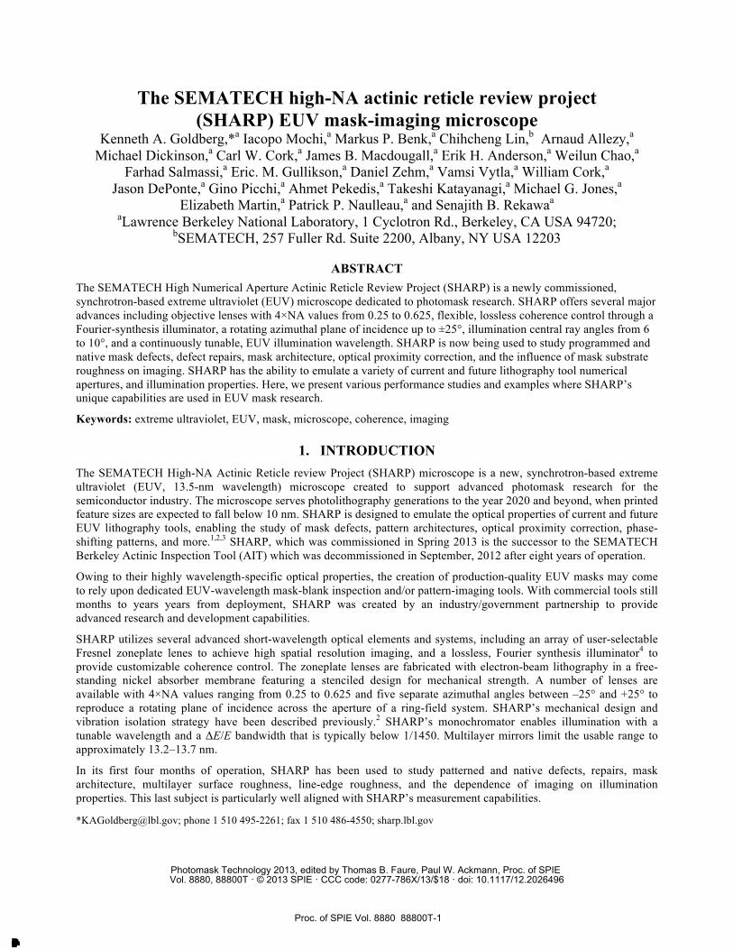
Illumination coherence is central to imaging in photolithography. Coherence has a strong effect on the appearance of defect repairs and printability, multilayer and line-edge roughness, optical proximity corrections, and the basic properties of contrast and image slope for patterns, especially at small sizes. Data from SHARP is used to calibrate modeling and to provide aerial image information for comparison with wafer printing.
Beam in focus (dot at 6 o’clock) Lissajous pattern covering Mc 0.5 NA (8°), 0.8 σ, 15 rings 0.5 NA (8°), 1.0 σ, 19 rings
0.5 NA (8°), 1.2 σ 0.625 NA (10°), 1.0 σ, 10° CRA 0.625 NA (10°), 0.8 σ, 10° CRA 0.625 NA (10°), 0.8 σ, +25° azi
0.625 NA (10°), 0.8 σ, –25° azi smallest angular divergence 0.25 NA (6°), 1.0 σ 0.25 NA (6°), 0.2 σ
0.25 NA (6°), 0.047 σ, smallest fill 0.5 NA (8°), 0.2–0.8 σ, annular 0.5 NA (8°), 0.8 σ, dipole 0.5 NA (8°), 0.8 σ, 45° dipole
0.5 NA (8°), 0.5 σ, quadrupole 0.5 NA (8°), 0.5 σ, 45° quadrupole 0.5 NA (8°), 0.8 σ, crosspole 22.5° 0.5 NA (8°), 0.8 σ, crosspole 45°
0.5 NA (8°), 0.4–0.8 σ, crosspole 45° 0.5 NA (8°), 0.4–0.8 σ, crossp. 10° 0.5 NA (8°), 0.1–1 σ, 0.5 NA (8°), 0.4–0.8 σ 45° crosspole, 22.5° 45° crosspole, 22.5°
Figure 1. Demonstration of (angular) pupil fill patterns, recorded with EUV light on the pupil-fill monitor. Patterns are drawn during each exposure.
Proc. of SPIE Vol. 8880 88800T-2
Downloaded From: http://proceedings.spiedigitallibrary.org/ on 10/04/2013 Terms of Use: http://spiedl.org/terms

In addition to now-routine operations in support of SEMATECH member company users, we are conducting experiments to characterize and improve the performance of the various sub-systems over time. Here we present several experiemntal demonstrations of the capabilities of SHARP, and a small sampling of data collected with the tool.
2. FOURIER-SYNTHESIS ILLUMINATOR SHARP’s Fourier-synthesis illuminator4 uses three multilayer-coated mirrors to convert the synchrotron beamline’s inherent low-divergence beam into arbitrary off-axis angular patterns ranging from 1 to 20° supporting central ray angles up to 10° (mask side). The first mirror, MA, is a 1-mm-diameter MEMS mirror mounted on a two-axis actuator that is capable of scannnig an angular range of ±4° at frequencies up to 2 kHz.3 Within each exposure, we scan an illumination pattern to create customized partial coherence ‘fill patterns.’ The beamline is focused onto MA, with a beam size of approximately 250 µm that can be reduced using a pair of xy slits, close to the mirror. The second mirror, MB, is a flat folding mirror that steers the beam upward into a condenser. Its purpose is to minimize the angles of incidence on the condenser, MC. The condenser is an off-axis ellipsoid with a graded multilayer coating. The condenser provides a 10x demagnification, reimaging the beam spot from MA onto the mask. In other words, MC focuses every ray that leaves MA, to a demagnified beam spot on the mask surface.
To visualize and calibrate the illumination, SHARP has a low-magnification (1.7x), in-vacuum, YAG microscope mounted to the mask stage, called the pupil-fill monitor. The YAG crystal converts the incident EUV beam into visible light, which is reimaged by the microscope. The mask stage allows the YAG to be placed into the focal plane of the illuminator, where the rays converge to a single point. Beam angles are calculated by measuring the light in two longitudinal planes: the focal plane, and a plane 5 mm lower.
Examples of vaious pupil-fill patterns are shown in Fig. 1. Positions in the images correspond to off-axis angles. Here, angles in the central plane of incidence would be along the y-axis in the center of the image. The smallest static angle is 2.96 mrad, which corresponds to 0.047 σ at 0.25 4×NA, or 0.019 σ at 0.625 4×NA.
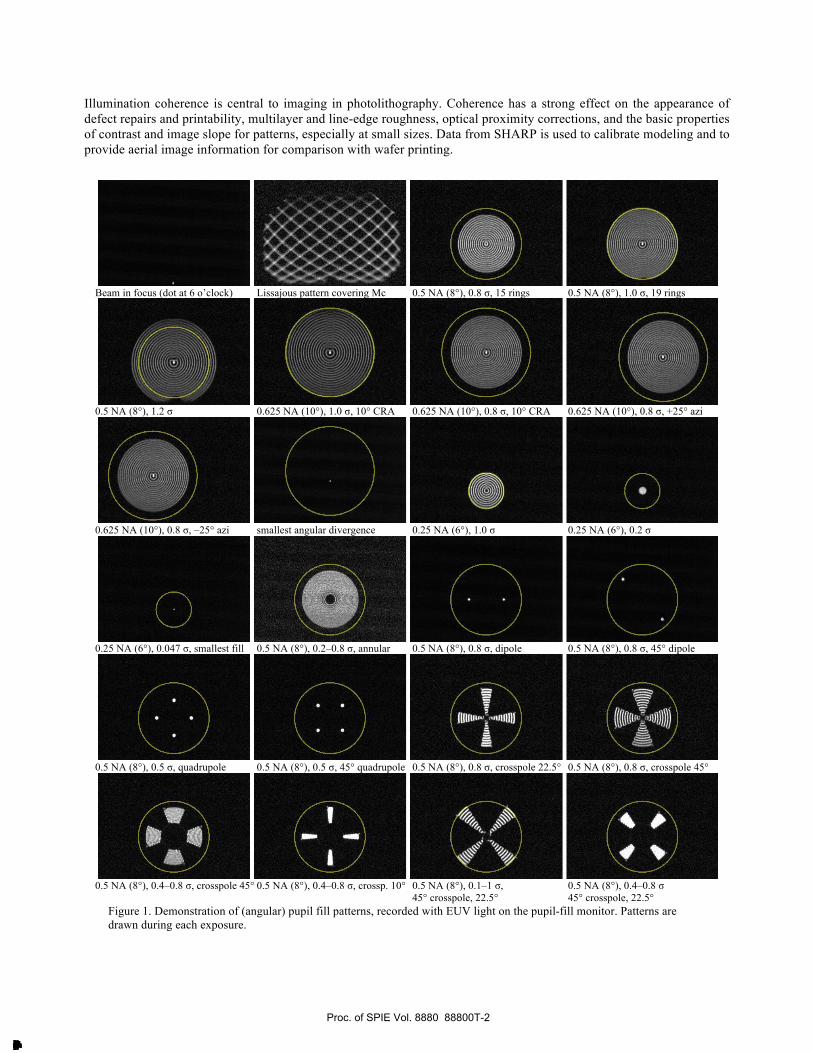
3. DEMONSTRATION OF PARTIAL COHERENCE EFFECTS IN IMAGING In SHARP images, the effects of illumination partial coherence are readily observable, giving insight into the nature of image formation. All illumination patterns may be understood as an additive synthesis of off-axis monopoles, a point that underlies the operation of the Fourier-synthesis illuminator.5 Here we first study the pattern imaging from a coherent, off-axis monopole illumination. We then consider line imaging under varying partial coherence. Finally, we observe the effect of increasing the NA while preserving constant illumination conditions.
3.1 On-axis and off-axis monopole illumination
Figure 2 contains a series of images of the same elbow-pattern test object recorded with different illumination settings. For these experiments a 100-nm half-pitch elbow pattern was used with a 4×NA value of 0.33. With coherent illumination (Fig. 2a) the features are clear and well resolved. However, off-axis monopole illumination, with 0.1 σ, and a relative offset magnitude of 0.8, causes significant changes. Readily observable is the loss of resolution of features parallel to the off-axis direction. This behavior is readily understood from the perspective of Fourier optics, wherein the lens pupil behaves as an angle-space filter on the imaging. For dense, line pattern features to be resolved by a lens, the diffraction orders must pass into the pupil. Those diffraction orders follow the angle offset of the central ray. So, when the central ray is close to the edge of the pupil’s solid angle, diffraction orders falling in the direction perpendicular to the offset angle can be clipped by the pupil. The images in Fig. 2c, d, e, and f show how the rotation of the illumination selectively filters different line orientations in the pattern. For comparison, Fig. 2b shows imaging annular illumination, which may be considered as the synthesis of a continuous ring of off-axis angles. With annular illumination, the contrast in these small features is reduced, but the depth of focus (not shown) can be enhanced.
Proc. of SPIE Vol. 8880 88800T-3
Downloaded From: http://proceedings.spiedigitallibrary.org/ on 10/04/2013 Terms of Use: http://spiedl.org/terms
a) coherent
b) annular
c) off-axis monopole, 180°
d) off-axis monopole, 135°
e) off-axis monopole, 90°
f) off-axis monopole, 45°
Figure 2. Demonstrations of coherent on-axis and off-axis monopole illumination of an elbow test-pattern. The black circles represent the full pupil, and the white dot the illumination angle and size within it. The patterns have 100-nm half-pitch, and were imaged using 0.33 4×NA. (b) Annular illumination with the same offset angle.
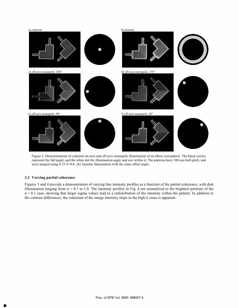
3.2 Varying partial coherence
Figures 3 and 4 provide a demonstration of varying line intensity profiles as a function of the partial coherence, with disk illumination ranging from σ = 0.1 to 1.0. The intensity profiles in Fig. 4 are normalized to the brightest portions of the σ = 0.1 case, showing that larger sigma values lead to a redistribution of the intensity within the pattern. In addition to the contrast differences, the reduction of the image intensity slope in the high σ cases is apparent.
Proc. of SPIE Vol. 8880 88800T-4
Downloaded From: http://proceedings.spiedigitallibrary.org/ on 10/04/2013 Terms of Use: http://spiedl.org/terms
a) σ = 0.1
b) σ = 0.4
c) σ = 0.7
d) σ = 1.0
Figure 3. Circle grating images recorded with varying disk fill patterns. The gratings have 110-nm half-pitch, and are imaged by a 0.33-4×NA lens.
Figure 4. Line intensity profiles extracted from the circle grating pattern in the 3 o’clock position. The profiles share a common intensity normalization, showing that the coherent light (σ = 0.1) has the globally highest peaks. At this line size and NA, higher σ values are associated with reduced contrast, and lower image intensity slope. (Color online.)
3.3 Varying numerical aperture
Imaging of fine patterns depends strongly on the ways in which the various diffraction orders are transmitted or are filtered by the lens. A series of measurements conducted on SHARP reveals how the lens numerical aperture affects line
0.10.40.71.0
σ
0.1 σ
0.4 σ
0.7 σ
1.0 σ
inte
nsity
0
0.2
0.4
0.6
0.8
1.0
position [nm]−300 −250 −200 −150 −100 −50 0 50 100 150 200 250 300
Proc. of SPIE Vol. 8880 88800T-5
Downloaded From: http://proceedings.spiedigitallibrary.org/ on 10/04/2013 Terms of Use: http://spiedl.org/terms
N.
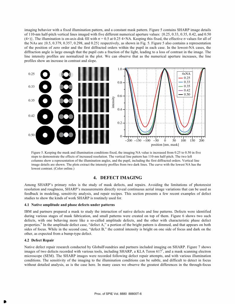
imaging behavior with a fixed illumination pattern, and a constant mask pattern. Figure 5 contains SHARP image details of 110-nm half-pitch vertical lines imaged with five different numerical aperture values: {0.25, 0.33, 0.35, 0.42, and 0.50 (4×)}. The illumination is on-axis disk fill with σ = 0.5 at 0.25 4×NA. Keeping this fixed, the effective σ values for all of the NAs are {0.5, 0.379, 0.357, 0.298, and 0.25} respectively, as shown in Fig. 5. Figure 5 also contains a representation of the position of zero order and the first diffracted orders within the pupil in each case. In the lowest-NA cases, the diffraction angle is large enough that the pupil cuts a fraction of the light, leading to a loss of contrast in the image. The line intensity profiles are normalized in the plot. We can observe that as the numerical aperture increases, the line profiles show an increase in contrast and slope.
Figure 5. Keeping the mask and illumination conditions fixed, the imaging NA value is increased from 0.25 to 0.50 in five steps to demonstrate the effects of increased resolution. The vertical line pattern has 110-nm half-pitch. The two left columns show a representation of the illumination angles, and the pupil, including the first diffracted orders. Vertical line image details are shown. The plots extract the intensity profiles from two dark lines. The curve with the lowest NA has the lowest contrast. (Color online.)
4. DEFECT IMAGING Among SHARP’s primary roles is the study of mask defects, and repairs. Avoiding the limitations of photoresist resolution and roughness, SHARP’s measurements directly reveal continuous aerial image variations that can be used as feedback in modeling, sensitivity analysis, and repair recipes. This section presents a few recent examples of defect studies to show the kinds of work SHARP is routinely used for.
4.1 Native amplitude and phase defects under patterns
IBM and partners prepared a mask to study the interaction of native defects and line patterns. Defects were identified during various stages of mask fabrication, and small patterns were created on top of them. Figure 6 shows two such defects, with one behaving more like a so-called amplitude defects, and the other with characteristic phase defect properties.6 In the amplitude defect case, “defect A,” a portion of the bright pattern is dimmed, and that appears on both sides of focus. While in the second case, “defect B,” the central intensity is bright on one side of focus and dark on the other, as expected from a bump-type defect.
4.2 Defect Repair
Native defect repair research conducted by GlobalFoundries and partners included imaging on SHARP. Figure 7 shows images of two defects recorded with various tools, including SHARP, a KLA Teron 6177, and a mask scanning electron microscope (SEM). The SHARP images were recorded following defect repair attempts, and with various illumination conditions. The sensitivity of the imaging to the illumination conditions can be subtle, and difficult to detect in focus without detailed analysis, as is the case here. In many cases we observe the greatest differences in the through-focus
0.250.330.350.420.50
4xNA0.25
0.33
0.35
0.42
0.50
inte
nsity
0
0.2
0.4
0.6
0.8
1.0
position [nm, mask]−200 −150 −100 −50 0 50 100 150 200
Proc. of SPIE Vol. 8880 88800T-6
Downloaded From: http://proceedings.spiedigitallibrary.org/ on 10/04/2013 Terms of Use: http://spiedl.org/terms

F
''fiti .rr¡.
- r A. f
a) Mask/KLA617 Teron
b) Mask/KLA617 Teron
Mask /SEM
Mask /SEM
1!
SHARP, quasar 45°
Mr
SHARP, quasar 45°
1111
SHARP, annular SHARP, disk 0.9 o
SHARP, annular
.5µm
1.5µm
behavior of the different illumination conditions. In particular, the apparent depth of focus, and the manner in which the defects blur in the out-of-focus images can be observably different.
Figure 6. Native defect imaging through focus, created by patterning 160-nm half-pitch lines above known defects. (a) Defect A shows characteristic behaviors of an amplitude defect. (b) Defect B shows behavior associated with bump-type phase defects, with a reversal of the apparent intensity on either side of best focus. Lines were imaged with a 4×NA value of 0.33, and 0.5-µm steps through focus.
Figure 7. Two native mask defects imaged with various tools, including the KLA617 Teron tool, mask SEM, and SHARP with multiple illumination conditions. (a) Defect in 110-nm half-pitch lines, repaired prior to imaging in SHARP. Images recorded with various illumination conditions show subtle differences. (b) Defect in 200-nm half-pitch lines, repaired before SHARP measurement. Lines were imaged with a 4×NA of 0.33, and various illumination conditions indicated in the figure.
(a) Defect A
through focus
(c) Defect A 2.0 �m
(d) Defect B
(b) Defect B
Proc. of SPIE Vol. 8880 88800T-7
Downloaded From: http://proceedings.spiedigitallibrary.org/ on 10/04/2013 Terms of Use: http://spiedl.org/terms
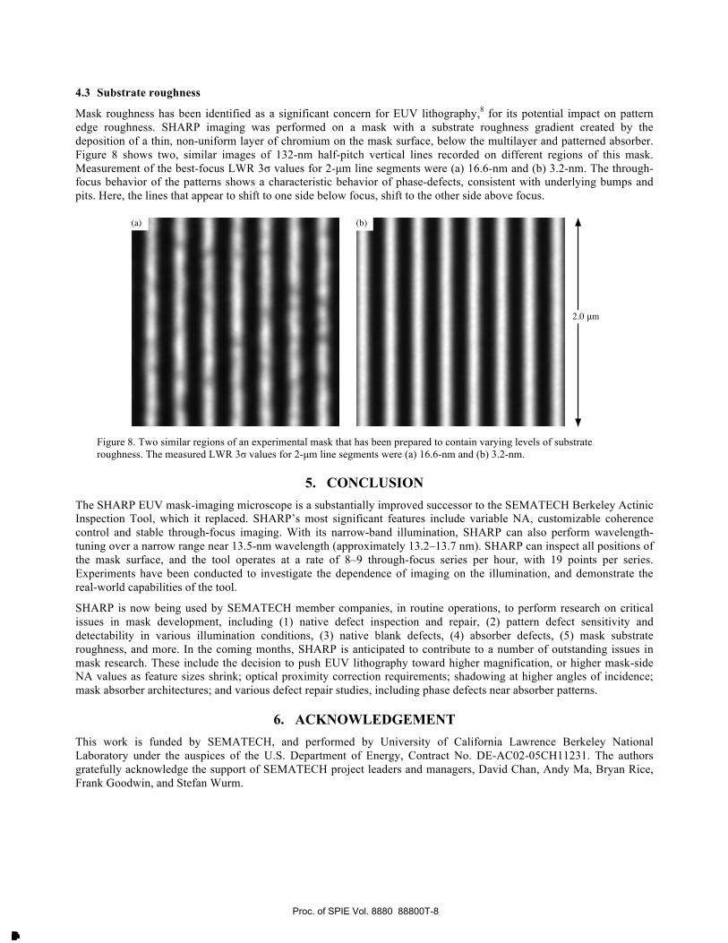
4.3 Substrate roughness
Mask roughness has been identified as a significant concern for EUV lithography,8 for its potential impact on pattern edge roughness. SHARP imaging was performed on a mask with a substrate roughness gradient created by the deposition of a thin, non-uniform layer of chromium on the mask surface, below the multilayer and patterned absorber. Figure 8 shows two, similar images of 132-nm half-pitch vertical lines recorded on different regions of this mask. Measurement of the best-focus LWR 3σ values for 2-µm line segments were (a) 16.6-nm and (b) 3.2-nm. The through-focus behavior of the patterns shows a characteristic behavior of phase-defects, consistent with underlying bumps and pits. Here, the lines that appear to shift to one side below focus, shift to the other side above focus.
Figure 8. Two similar regions of an experimental mask that has been prepared to contain varying levels of substrate roughness. The measured LWR 3σ values for 2-µm line segments were (a) 16.6-nm and (b) 3.2-nm.
5. CONCLUSION The SHARP EUV mask-imaging microscope is a substantially improved successor to the SEMATECH Berkeley Actinic Inspection Tool, which it replaced. SHARP’s most significant features include variable NA, customizable coherence control and stable through-focus imaging. With its narrow-band illumination, SHARP can also perform wavelength-tuning over a narrow range near 13.5-nm wavelength (approximately 13.2–13.7 nm). SHARP can inspect all positions of the mask surface, and the tool operates at a rate of 8–9 through-focus series per hour, with 19 points per series. Experiments have been conducted to investigate the dependence of imaging on the illumination, and demonstrate the real-world capabilities of the tool.
SHARP is now being used by SEMATECH member companies, in routine operations, to perform research on critical issues in mask development, including (1) native defect inspection and repair, (2) pattern defect sensitivity and detectability in various illumination conditions, (3) native blank defects, (4) absorber defects, (5) mask substrate roughness, and more. In the coming months, SHARP is anticipated to contribute to a number of outstanding issues in mask research. These include the decision to push EUV lithography toward higher magnification, or higher mask-side NA values as feature sizes shrink; optical proximity correction requirements; shadowing at higher angles of incidence; mask absorber architectures; and various defect repair studies, including phase defects near absorber patterns.
6. ACKNOWLEDGEMENT This work is funded by SEMATECH, and performed by University of California Lawrence Berkeley National Laboratory under the auspices of the U.S. Department of Energy, Contract No. DE-AC02-05CH11231. The authors gratefully acknowledge the support of SEMATECH project leaders and managers, David Chan, Andy Ma, Bryan Rice, Frank Goodwin, and Stefan Wurm.
(a) (b)
2.0 μm
Proc. of SPIE Vol. 8880 88800T-8
Downloaded From: http://proceedings.spiedigitallibrary.org/ on 10/04/2013 Terms of Use: http://spiedl.org/terms

REFERENCES
[1] K. A. Goldberg, I. Mochi, S. B. Rekawa, N. S. Smith, J. B. Macdougall, P. P. Naulleau, “An EUV Fresnel zoneplate mask-imaging microscope for lithography generations reaching 8 nm,” Proc. SPIE 7969, 79691O (2011).
[2] K. A. Goldberg, I. Mochi, M. P. Benk, A. P. Allezy, N. S. Smith, C. W. Cork, W. Cork, J. Macdougall, W. L. Chao, E. H. Anderson, P. P. Naulleau, E. Acome, E. Van Every, V. Milanovic, S. B. Rekawa, “Creating an EUV Mask Microscope for Lithography Generations Reaching 8 nm,” Precision Engineering and Mechatronics Supporting the Semiconductor Industry, 4–7 (2012).
[3] K. A. Goldberg, I. Mochi, M. Benk, A. P. Allezy, M. R. Dickinson, C. W. Cork, D. Zehm, J. B. Macdougall, E. Anderson, F. Salmassi, W. L. Chao, V. K. Vytla, E. M. Gullikson, J. C. DePonte, M. S. Jones, D. Van Camp, J. F. Gamsby, W. B. Ghiorso, H. Huang, W. Cork, E. Martin, E. Van Every, E. Acome, V. Milanovic, R. Delano, P. P. Naulleau, and S. B. Rekawa, “Commissioning an EUV mask microscope for lithography generations reaching 8 nm,” Proc. SPIE 8679, 867919 (2013).
[4] P. Naulleau, K. Goldberg, P. Batson, J. Bokor, P. Denham, and S. Rekawa, “A Fourier-synthesis custom-coherence illuminator for EUV microfield lithography,” Appl. Opt. 42 (5), 820–26 (2003).
[5] Goodman, J. W., [Statistical Optics], John Wiley & Sons, Inc., New York, 303–7 (2000). [6] I. Mochi, K. A. Goldberg, S. Huh, “Actinic imaging and evaluation of phase structures on EUV lithography masks,”
J. Vac. Sci. Technol. B 28 (6), C6E11-16 (2010). [7] U. Okoroanyanwu, J. Heumann, X. Zhu, C. H. Clifford, F. Jiang, P. Mangat, R. Ghaskadavi, E. Mohn, R. Moses, O.
Wood, H. Rolff, T. Schedel, R. Cantrell, P. Nesladek, N. LiCausi, X. Cai, W. Taylor, J. Schefske, M. Bender, N. Schmidt, “Towards the Optical Inspection Sensitivity Optimization of EUV Masks and EUVL-Exposed Wafers,” Proc. SPIE 8352, 83520V (2012).
[8] P. P. Naulleau, K. A. Goldberg, E. Gullikson, I. Mochi, B. McClinton, and A. Rastegar, “Accelerating EUV learning with synchrotron light: mask roughness challenges ahead,” Proc. SPIE 8166, 81660F (2011).
Proc. of SPIE Vol. 8880 88800T-9
Downloaded From: http://proceedings.spiedigitallibrary.org/ on 10/04/2013 Terms of Use: http://spiedl.org/terms