acpl-p343 and acpl-w343 - farnell element14 · broadcom - 2 - acpl-p343 and acpl-w343 data sheet...
TRANSCRIPT
ACPL-P343 and ACPL-W3434.0 Amp Output Current IGBT Gate Drive Optocoupler with Rail-to-Rail Output Voltage in Stretched SO6
Data Sheet
DescriptionThe ACPL-P343/W343 contains an AlGaAs LED, which is optically coupled to an integrated circuit with a power output stage. This optocoupler is ideally suited for driving power IGBTs and MOSFETs used in motor control inverter applications. The high operating voltage range of the output stage provides the drive voltages required by gate controlled devices. The voltage and high peak output current supplied by this optocoupler make it ideally suited for direct driving IGBT with ratings up to 1200V/200A. For IGBTs with higher ratings, this optocoupler can be used to drive a discrete power stage which drives the IGBT gate. The ACPL-P343 and ACPL-W343 have the highest insulation voltage of VIORM = 891 Vpeak and VIORM = 1140 Vpeak, respectively, in the IEC/EN/DIN EN 60747-5-5.
Features 4.0-A maximum peak output current 3.0-A minimum peak output current Rail-to-rail output voltage 200-ns maximum propagation delay 100-ns maximum propagation delay difference LED current input with hysteresis 35 kV/μs minimum Common Mode Rejection (CMR) at
VCM = 1500V ICC = 3.0 mA maximum supply current Under voltage lock-out protection (UVLO) with hysteresis Wide operating VCC range: 15V to 30V Industrial temperature range: –40°C to 105°C Safety approval:
— UL Recognized 3750/5000 VRMS for 1 min.— CSA — IEC/EN/DIN EN 60747-5-5 VIORM = 891/1140 Vpeak
Applications IGBT/MOSFET gate drive AC and brushless DC motor drives Renewable energy inverters Industrial inverters Switching power supplies
CAUTION: It is advised that normal static precautions be taken in handling and assembly of this component to prevent damage and/or degradation that may be induced by ESD. The components featured in this data sheet are not to be used in military or aerospace applications or environments.
Broadcom- 1 -
ACPL-P343 and ACPL-W343 Data Sheet
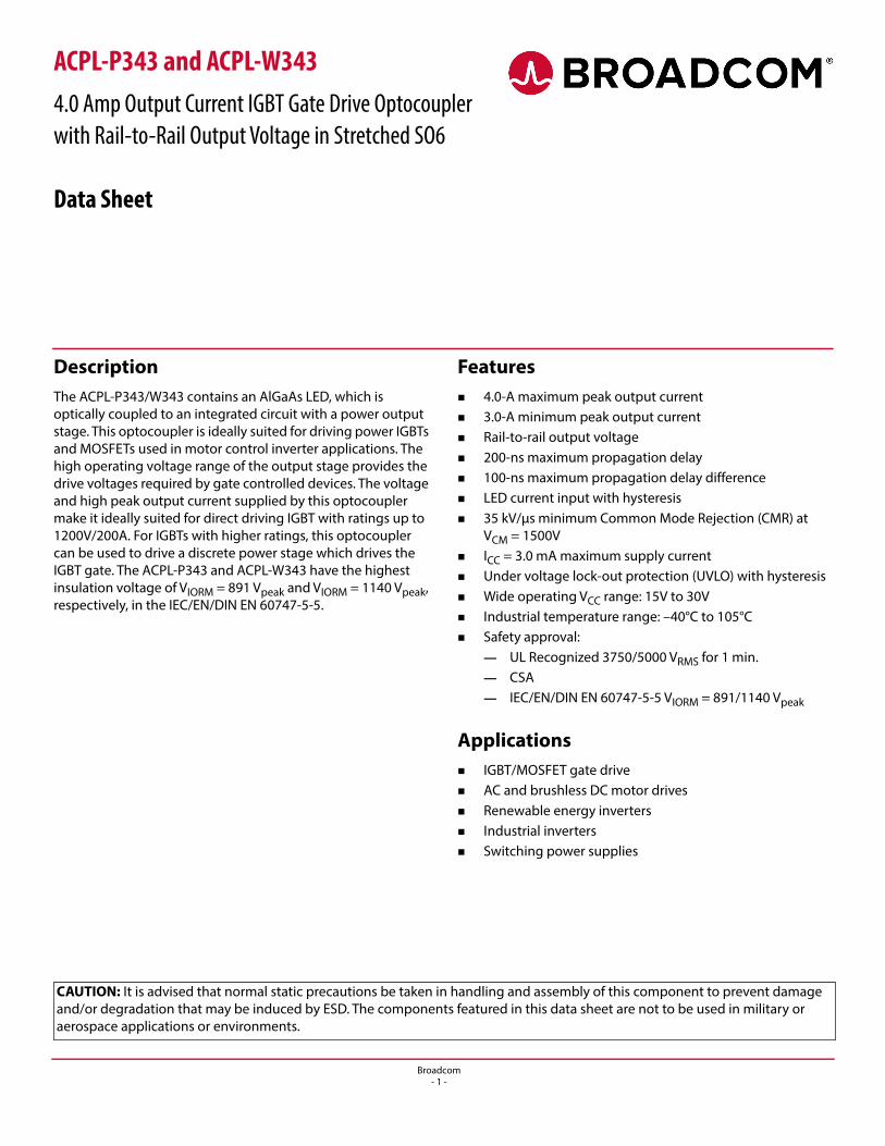
Functional DIagram
NOTE A 1-μF bypass capacitor must be connected between pins VCC and VEE.
Truth Table
Ordering InformationACPL-P343 is UL Recognized with 3750 VRMS for 1 minute per UL1577.
ACPL-W343 is UL Recognized with 5000 VRMS for 1 minute per UL1577.
To order, choose a part number from the part number column and combine with the desired option from the option column to form an order entry.
Example 1:
ACPL-P343-560E to order product of Stretched SO-6 Surface Mount package in Tape and Reel packaging with IEC/EN/DIN EN 60747-5-5 Safety Approval in RoHS compliant.
Example 2:
ACPL-W343-000E to order product of Stretched SO-6 Surface Mount package in Tube packaging and RoHS compliant.
Option data sheets are available. Contact your Broadcom sales representative or authorized distributor for information.
LEDVCC – VEE
“POSITIVE GOING” (that is, TURN-ON)VCC – VEE
“NEGATIVE GOING” (that is, TURN-OFF)VO
OFF 0–30 V 0–30 V LOW
ON 0–12.1 V 0–11.1 V LOW
ON 12.1–13.5 V 11.1–12.4 V TRANSITION
ON 13.5–30 V 12.4–30 V HIGH
Part NumberOption
Package Surface Mount Tape and Reel IEC/EN/DIN EN 60747-5-5 QuantityRoHS Compliant
ACPL-P343 ACPL-W343
-000E Stretched SO-6 X 100 per tube
-500E X X 1000 per reel
-060E X X 100 per tube
-560E X X X 1000 per reel
VCC
VEE
1
2
3
6
5
4CATHODE
NC
ANODE
VOUT
CATHODE
NC
ANODE
Broadcom- 2 -
ACPL-P343 and ACPL-W343 Data Sheet
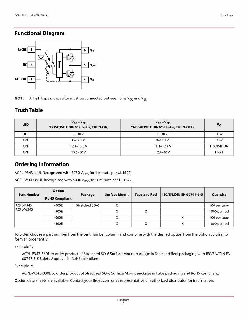
Package Outline Drawings
ACPL-P343 Stretched SO-6 Package (7-mm Clearance)
7°
7°
45°
5° NOM.
0.381 ±0.127(0.015 ±0.005)
1.27 (0.050) BSG*4.580 + 0.254
– 0
7°
7°
3.180 ±0.127(0.125 ±0.005)
1.590 ±0.127(0.063 ±0.005)
0.254 ±0.050(0.010 ±0.002)
9.7 ±0.250(0.382 ±0.010)
Floating Lead Protusions max. 0.25 (0.01)
Dimensions in Millimeters (Inches)
Lead Coplanarity = 0.1 mm (0.004 Inches)
* Total package length (inclusive of mold flash):
4.834 ± 0.254 (0.190 ± 0.010)
0.180 + 0.010– 0.000( )
1 ±0.250(0.040 ±0.010)
0.20 ±0.10(0.008 ±0.004)
7.62 (0.300)
6.81 (0.268)
0.45 (0.018)
10.7 (0.421)
1.27 (0.05)
0.76 (0.03)
2.16(0.085)
Land Pattern Recommendation
Broadcom- 3 -
ACPL-P343 and ACPL-W343 Data Sheet
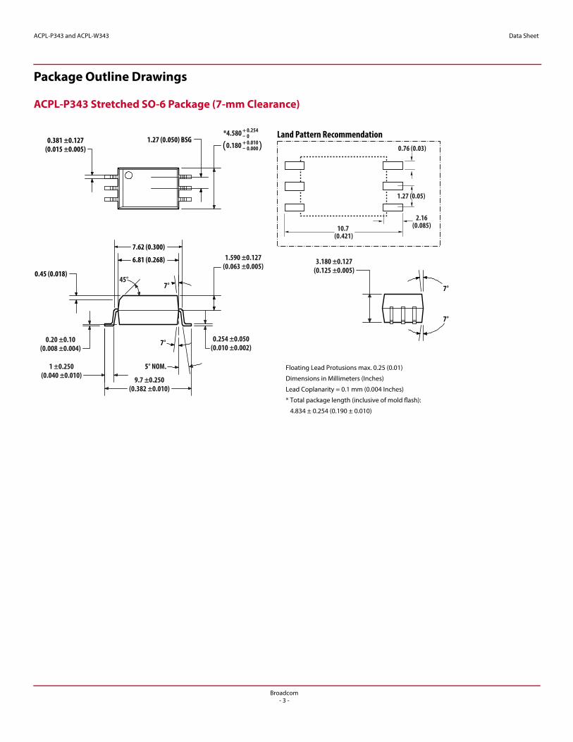
ACPL-W343 Stretched SO-6 Package (8-mm Clearance)
Recommended Pb-Free IR ProfileRecommended reflow condition as per JEDEC Standard, J-STD-020 (latest revision). Non- Halide Flux should be used.
Regulatory InformationThe ACPL-P343/W343 is approved by the following organizations:
UL
Recognized under UL 1577, component recognition program up to VISO = 3750 VRMS (ACPL-P343) and VISO = 5000 VRMS (ACPL-W343) expected prior to product release.
CSA
CSA Component Acceptance Notice #5, File CA 88324
IEC/EN/DIN EN 60747-5-5 (Option 060 Only)
Maximum Working Insulation Voltage VIORM = 891 Vpeak (ACPL-P343) and VIORM = 1140 Vpeak (ACPL-W343)
45°7°
7°
2
1
3 4
5
6
7°
7°
0.381 ±0.127(0.015 ±0.005)
0.20 ±0.10(0.008 ±0.004)
Floating Lead Protusions max. 0.25 (0.01)
Dimensions in Millimeters (Inches)
Lead Coplanarity = 0.1 mm (0.004 Inches)
* Total package length (inclusive of mold flash)
4.834 ± 0.254 (0.190 ± 0.010)
*4.580 + 0.254– 0
0.180 + 0.010– 0.000( )
6.807 + 0.127– 0
0.268 + 0.005– 0.000( )
1.27 (0.050) BSG
35° NOM.
0.750 ±0.250(0.0295 ±0.010)
11.500 ±0.25(0.453 ±0.010)
0.254 ±0.050(0.010 ±0.002)
1.590 ±0.127(0.063 ±0.005)
3.180 ±0.127(0.125 ±0.005)
0.45 (0.018)
7.62 (0.300) 12.65(0.5)
1.27 (0.05)
0.76 (0.03)
1.905(0.075)
Land Pattern Recommendation
Broadcom- 4 -
ACPL-P343 and ACPL-W343 Data Sheet
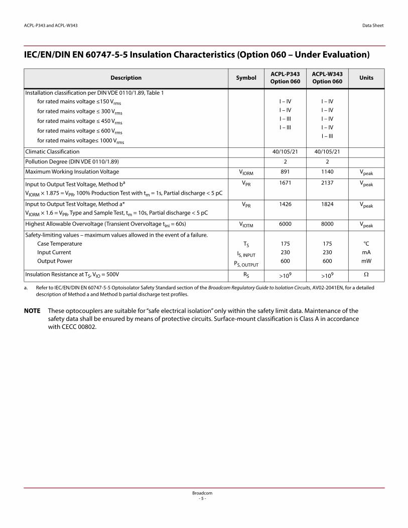
IEC/EN/DIN EN 60747-5-5 Insulation Characteristics (Option 060 – Under Evaluation)
NOTE These optocouplers are suitable for “safe electrical isolation” only within the safety limit data. Maintenance of the safety data shall be ensured by means of protective circuits. Surface-mount classification is Class A in accordance with CECC 00802.
Description Symbol ACPL-P343 Option 060
ACPL-W343 Option 060 Units
Installation classification per DIN VDE 0110/1.89, Table 1for rated mains voltage ≤150 Vrms
for rated mains voltage ≤ 300 Vrms
for rated mains voltage ≤ 450 Vrms
for rated mains voltage ≤ 600 Vrms
for rated mains voltage≤ 1000 Vrms
I – IVI – IVI – IIII – III
I – IVI – IVI – IVI – IVI – III
Climatic Classification 40/105/21 40/105/21
Pollution Degree (DIN VDE 0110/1.89) 2 2
Maximum Working Insulation Voltage VIORM 891 1140 Vpeak
Input to Output Test Voltage, Method ba
VIORM × 1.875 = VPR, 100% Production Test with tm = 1s, Partial discharge < 5 pC
a. Refer to IEC/EN/DIN EN 60747-5-5 Optoisolator Safety Standard section of the Broadcom Regulatory Guide to Isolation Circuits, AV02-2041EN, for a detailed description of Method a and Method b partial discharge test profiles.
VPR 1671 2137 Vpeak
Input to Output Test Voltage, Method a*VIORM × 1.6 = VPR, Type and Sample Test, tm = 10s, Partial discharge < 5 pC
VPR 1426 1824 Vpeak
Highest Allowable Overvoltage (Transient Overvoltage tini = 60s) VIOTM 6000 8000 Vpeak
Safety-limiting values – maximum values allowed in the event of a failure.Case TemperatureInput CurrentOutput Power
TS
IS, INPUT
PS, OUTPUT
175230600
175230600
°CmAmW
Insulation Resistance at TS, VIO = 500V RS >109 >109
Broadcom- 5 -
ACPL-P343 and ACPL-W343 Data Sheet
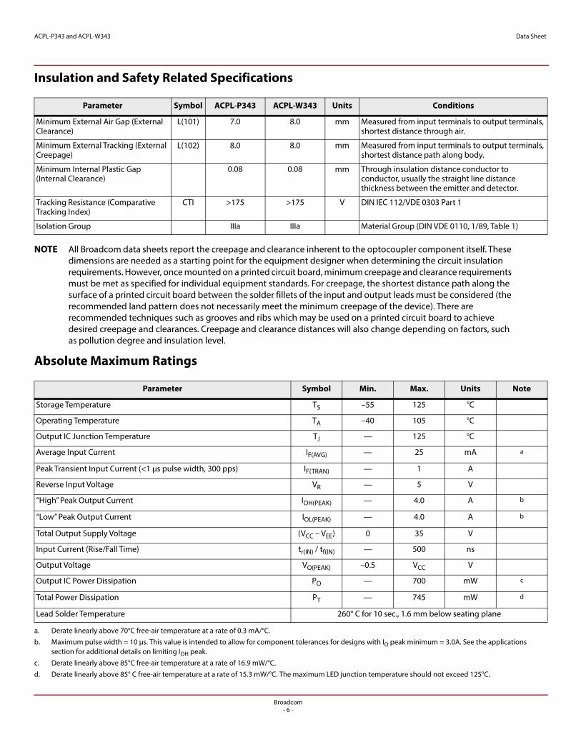
Insulation and Safety Related Specifications
NOTE All Broadcom data sheets report the creepage and clearance inherent to the optocoupler component itself. These dimensions are needed as a starting point for the equipment designer when determining the circuit insulation requirements. However, once mounted on a printed circuit board, minimum creepage and clearance requirements must be met as specified for individual equipment standards. For creepage, the shortest distance path along the surface of a printed circuit board between the solder fillets of the input and output leads must be considered (the recommended land pattern does not necessarily meet the minimum creepage of the device). There are recommended techniques such as grooves and ribs which may be used on a printed circuit board to achieve desired creepage and clearances. Creepage and clearance distances will also change depending on factors, such as pollution degree and insulation level.
Absolute Maximum Ratings
Parameter Symbol ACPL-P343 ACPL-W343 Units Conditions
Minimum External Air Gap (External Clearance)
L(101) 7.0 8.0 mm Measured from input terminals to output terminals, shortest distance through air.
Minimum External Tracking (External Creepage)
L(102) 8.0 8.0 mm Measured from input terminals to output terminals, shortest distance path along body.
Minimum Internal Plastic Gap (Internal Clearance)
0.08 0.08 mm Through insulation distance conductor to conductor, usually the straight line distance thickness between the emitter and detector.
Tracking Resistance (Comparative Tracking Index)
CTI >175 >175 V DIN IEC 112/VDE 0303 Part 1
Isolation Group IIIa IIIa Material Group (DIN VDE 0110, 1/89, Table 1)
Parameter Symbol Min. Max. Units Note
Storage Temperature TS –55 125 °C
Operating Temperature TA –40 105 °C
Output IC Junction Temperature TJ — 125 °C
Average Input Current IF(AVG) — 25 mA a
a. Derate linearly above 70°C free-air temperature at a rate of 0.3 mA/°C.
Peak Transient Input Current (<1 μs pulse width, 300 pps) IF(TRAN) — 1 A
Reverse Input Voltage VR — 5 V
“High” Peak Output Current IOH(PEAK) — 4.0 A b
b. Maximum pulse width = 10 μs. This value is intended to allow for component tolerances for designs with IO peak minimum = 3.0A. See the applications section for additional details on limiting IOH peak.
“Low” Peak Output Current IOL(PEAK) — 4.0 A b
Total Output Supply Voltage (VCC – VEE) 0 35 V
Input Current (Rise/Fall Time) tr(IN) / tf(IN) — 500 ns
Output Voltage VO(PEAK) –0.5 VCC V
Output IC Power Dissipation PO — 700 mW c
c. Derate linearly above 85°C free-air temperature at a rate of 16.9 mW/°C.
Total Power Dissipation PT — 745 mW d
d. Derate linearly above 85° C free-air temperature at a rate of 15.3 mW/°C. The maximum LED junction temperature should not exceed 125°C.
Lead Solder Temperature 260° C for 10 sec., 1.6 mm below seating plane
Broadcom- 6 -
ACPL-P343 and ACPL-W343 Data Sheet
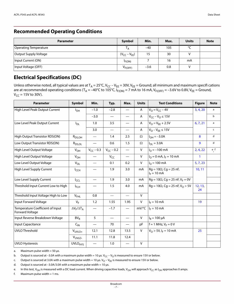
Recommended Operating Conditions
Electrical Specifications (DC)Unless otherwise noted, all typical values are at TA = 25°C, VCC – VEE = 30V, VEE = Ground; all minimum and maximum specifi cations are at recommended operating conditions (TA = –40°C to 105°C, IF(ON) = 7 mA to 16 mA, VF(OFF) = –3.6V to 0.8V, VEE = Ground, VCC = 15V to 30V).
Parameter Symbol Min. Max. Units Note
Operating Temperature TA –40 105 °C
Output Supply Voltage (VCC – VEE) 15 30 V
Input Current (ON) IF(ON) 7 16 mA
Input Voltage (OFF) VF(OFF) –3.6 0.8 V
Parameter Symbol Min. Typ. Max. Units Test Conditions Figure Note
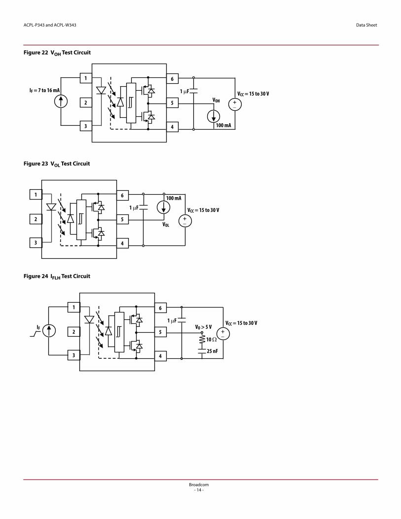
High Level Peak Output Current IOH –1.0 –2.8 — A VO = VCC – 4V 3, 4, 20 a
a. Maximum pulse width = 50 μs.
–3.0 — — A VCC – VO ≤ 15V b
b. Output is sourced at –3.0A with a maximum pulse width = 10 μs. VCC – VO is measured to ensure 15V or below.
Low Level Peak Output Current IOL 1.0 3.5 — A VO = VEE + 2.5V 6, 7, 21 a
3.0 — — A VO – VEE ≤ 15V c
c. Output is sourced at 3.0A with a maximum pulse width = 10 μs. VO – VEE is measured to ensure 15V or below.
High Output Transistor RDS(ON) RDS,OH — 1.4 2.5 IOH = –3.0A 8 d
d. Output is sourced at –3.0A/3.0A with a maximum pulse width = 10 μs.
Low Output Transistor RDS(ON) RDS,OL — 0.6 1.5 IOL = 3.0A 9 d
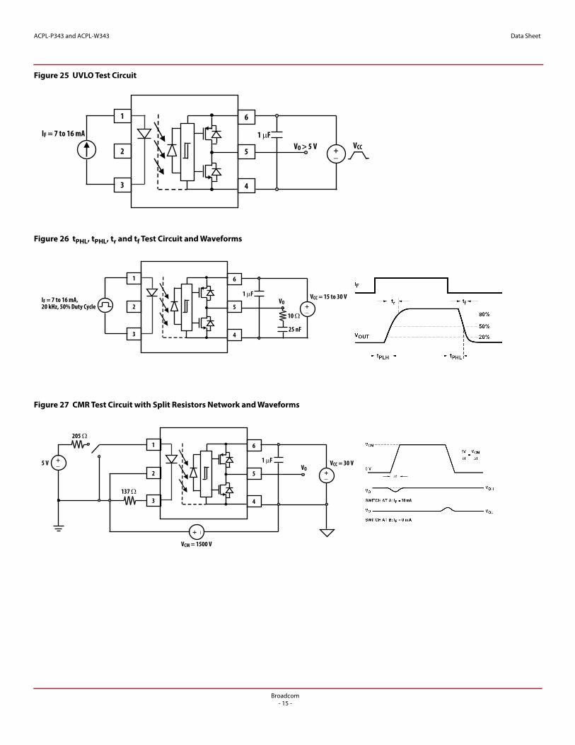
High Level Output Voltage VOH VCC – 0.3 VCC – 0.2 — V IO = –100 mA 2, 4, 22 e, f
e. In this test, VOH is measured with a DC load current. When driving capacitive loads, VOH will approach VCC as IOH approaches 0 amps.
f. Maximum pulse width = 1 ms.
High Level Output Voltage VOH — VCC — V IO = 0 mA, IF = 10 mA 1
Low Level Output Voltage VOL — 0.1 0.2 V IO = 100 mA 5, 7, 23
High Level Supply Current ICCH — 1.9 3.0 mA Rg = 10, Cg = 25 nF, IF = 10 mA
10, 11
Low Level Supply Current ICCL — 1.9 3.0 mA Rg = 10, Cg = 25 nF, VF = 0V
Threshold Input Current Low to High IFLH — 1.5 4.0 mA Rg = 10, Cg = 25 nF, VO > 5V 12, 13, 24
Threshold Input Voltage High to Low VFHL 0.8 — — V
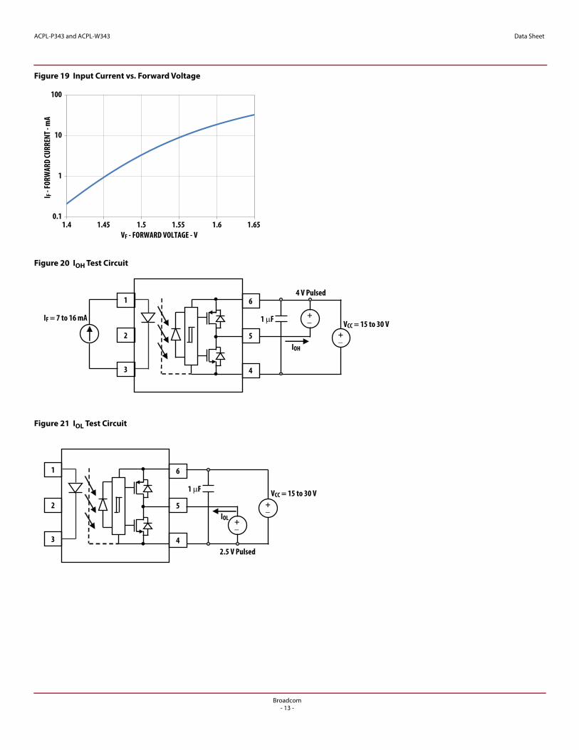
Input Forward Voltage VF 1.2 1.55 1.95 V IF = 10 mA 19
Temperature Coefficient of Input Forward Voltage
VF/TA — –1.7 — mV/°C IF = 10 mA
Input Reverse Breakdown Voltage BVR 5 — — V IR = 100 μA
Input Capacitance CIN — 70 — pF f = 1 MHz, VF = 0 V
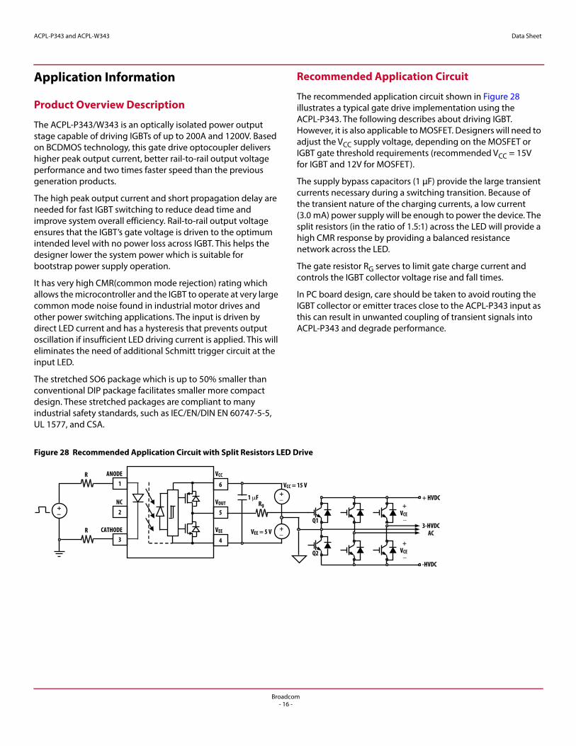
UVLO Threshold VUVLO+ 12.1 12.8 13.5 V VO > 5V, IF = 10 mA 25
VUVLO- 11.1 11.8 12.4
UVLO Hysteresis UVLOHYS — 1.0 — V
Broadcom- 7 -
ACPL-P343 and ACPL-W343 Data Sheet
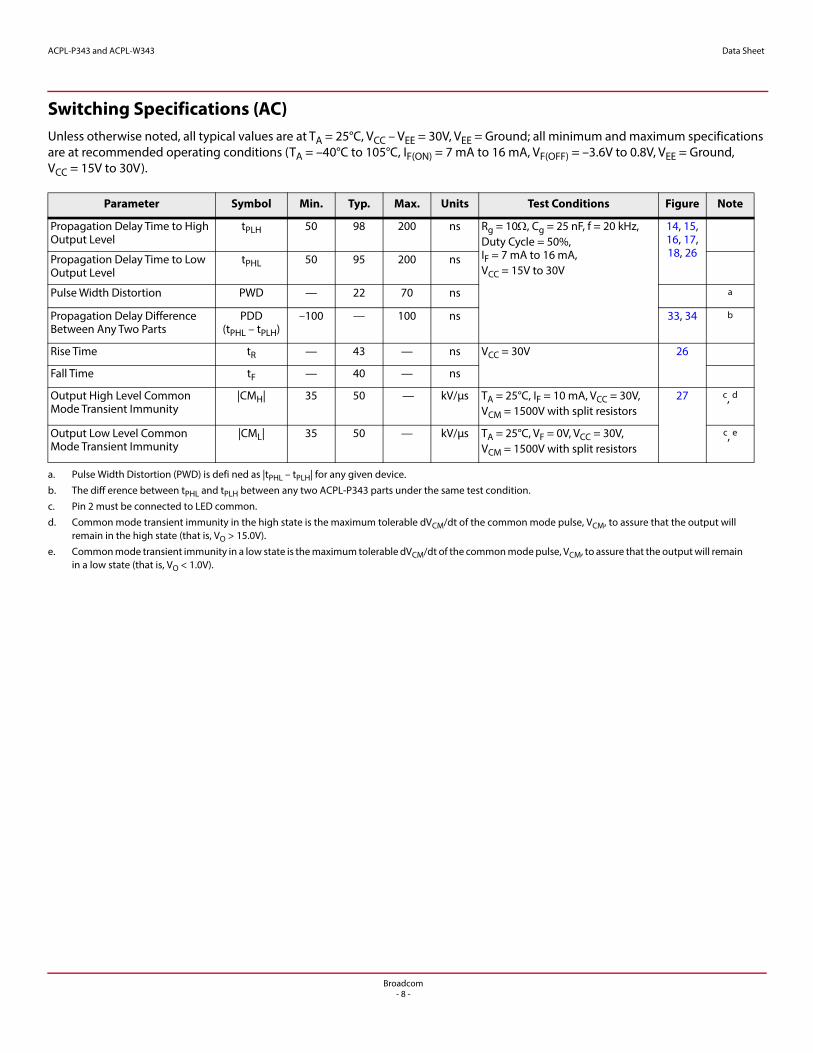
Switching Specifications (AC)Unless otherwise noted, all typical values are at TA = 25°C, VCC – VEE = 30V, VEE = Ground; all minimum and maximum specifications are at recommended operating conditions (TA = –40°C to 105°C, IF(ON) = 7 mA to 16 mA, VF(OFF) = –3.6V to 0.8V, VEE = Ground, VCC = 15V to 30V).
Parameter Symbol Min. Typ. Max. Units Test Conditions Figure Note
Propagation Delay Time to High Output Level
tPLH 50 98 200 ns Rg = 10, Cg = 25 nF, f = 20 kHz, Duty Cycle = 50%, IF = 7 mA to 16 mA,VCC = 15V to 30V
14, 15, 16, 17, 18, 26Propagation Delay Time to Low
Output LeveltPHL 50 95 200 ns
Pulse Width Distortion PWD — 22 70 ns a
a. Pulse Width Distortion (PWD) is defi ned as |tPHL – tPLH| for any given device.
Propagation Delay Difference Between Any Two Parts
PDD (tPHL – tPLH)
–100 — 100 ns 33, 34 b
b. The diff erence between tPHL and tPLH between any two ACPL-P343 parts under the same test condition.
Rise Time tR — 43 — ns VCC = 30V 26
Fall Time tF — 40 — ns
Output High Level Common Mode Transient Immunity
|CMH| 35 50 — kV/μs TA = 25°C, IF = 10 mA, VCC = 30V, VCM = 1500V with split resistors
27 c, d
c. Pin 2 must be connected to LED common.
d. Common mode transient immunity in the high state is the maximum tolerable dVCM/dt of the common mode pulse, VCM, to assure that the output will remain in the high state (that is, VO > 15.0V).
Output Low Level Common Mode Transient Immunity
|CML| 35 50 — kV/μs TA = 25°C, VF = 0V, VCC = 30V, VCM = 1500V with split resistors
c, e
e. Common mode transient immunity in a low state is the maximum tolerable dVCM/dt of the common mode pulse, VCM, to assure that the output will remain in a low state (that is, VO < 1.0V).
Broadcom- 8 -
ACPL-P343 and ACPL-W343 Data Sheet
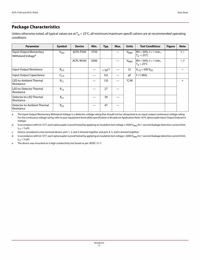
Package CharacteristicsUnless otherwise noted, all typical values are at TA = 25°C; all minimum/maximum specifi cations are at recommended operating conditions.
Parameter Symbol Device Min. Typ. Max. Units Test Conditions Figure Note
Input-Output Momentary Withstand Voltagea
a. The Input-Output Momentary Withstand Voltage is a dielectric voltage rating that should not be interpreted as an input-output continuous voltage rating. For the continuous voltage rating, refer to your equipment level safety specification or Broadcom Application Note 1074, Optocoupler Input-Output Endurance Voltage.
VISO ACPL-P343 3750 — VRMS RH < 50%, t = 1 min., TA = 25°C
b, c
b. In accordance with UL1577, each optocoupler is proof tested by applying an insulation test voltage ≤ 4500 VRMS for 1 second (leakage detection current limit, II-O < 5 μA).
c. Device considered a two-terminal device: pins 1, 2, and 3 shorted together and pins 4, 5, and 6 shorted together.
ACPL-W343 5000 — VRMS RH < 50%, t = 1 min., TA = 25°C
c, d
d. In accordance with UL1577, each optocoupler is proof tested by applying an insulation test voltage ≤ 6000 VRMS for 1 second (leakage detection current limit, II-O < 5 μA).
Input-Output Resistance RI-O — > 5012 — VI-O = 500 VDC c
Input-Output Capacitance CI-O — 0.6 — pF f =1 MHz
LED-to-Ambient Thermal Resistance
R11 — 135 — °C/W e
e. The device was mounted on a high conductivity test board as per JEDEC 51-7.
LED-to-Detector Thermal Resistance
R12 — 27 —
Detector-to-LED Thermal Resistance
R21 — 39 —
Detector-to-Ambient Thermal Resistance
R22 — 47 —
Broadcom- 9 -
ACPL-P343 and ACPL-W343 Data Sheet
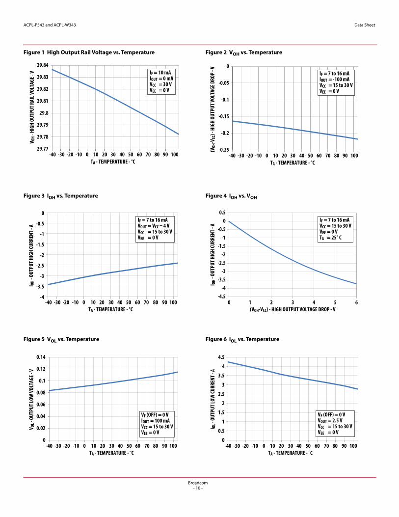
Figure 1 High Output Rail Voltage vs. Temperature Figure 2 VOH vs. Temperature
IF = 10 mAIOUT = 0 mAVCC = 30 VVEE = 0 V
29.84
29.81
29.82
29.83
29.77
29.78
29.79
29.8
-40 -30 -20 -10 0 10 20 30 40 50 60 70 80 90 100
V OH -
HIG
H OU
TPUT
RAI
L VOL
TAGE
- V
TA - TEMPERATURE - °C
IF = 7 to 16 mAIOUT = -100 mAVCC = 15 to 30 VVEE = 0 V
-40 -30 -20 -10 0 10 20 30 40 50 60 70 80 90 100TA - TEMPERATURE - °C
0
-0.15
-0.1
-0.05
-0.25
-0.2
(VOH
-VCC
) - H
IGH
OUTP
UT V
OLTA
GE D
ROP
- V
Figure 3 IOH vs. Temperature Figure 4 IOH vs. VOH
IF = 7 to 16 mAVOUT = VCC – 4 V VCC = 15 to 30 VVEE = 0 V
-40 -30 -20 -10 0 10 20 30 40 50 60 70 80 90 100TA - TEMPERATURE - °C
-0.5
0
-2
-1.5
-1
-4
-3.5
-3
-2.5
I OH -
OUT
PUT H
IGH
CURR
ENT -
A
IF = 7 to 16 mAVCC = 15 to 30 VVEE = 0 VTA = 25° C-1
-0.50
0.5
-3-2.5
-2-1.5
-4.5-4
-3.5
0 1 2 3 4 5 6
I OH -
OUT
PUT H
IGH
CURR
ENT -
A
(VOH-VCC) - HIGH OUTPUT VOLTAGE DROP - V
Figure 5 VOL vs. Temperature Figure 6 IOL vs. Temperature
VF (OFF) = 0 VIOUT = 100 mAVCC = 15 to 30 VVEE = 0 V
-40 -30 -20 -10 0 10 20 30 40 50 60 70 80 90 100TA - TEMPERATURE - °C
0.1
0.12
0.14
0.02
0.04
0.06
0.08
0
V OL -
OUT
PUT L
OW V
OLTA
GE - V
-40 -30 -20 -10 0 10 20 30 40 50 60 70 80 90 100TA - TEMPERATURE - °C
3
3.5
4
4.5
0.5
1
1.5
2
2.5
0
I OL -
OUT
PUT L
OW CU
RREN
T - A
VF (OFF) = 0 VVOUT = 2.5 V VCC = 15 to 30 VVEE = 0 V
Broadcom- 10 -
ACPL-P343 and ACPL-W343 Data Sheet
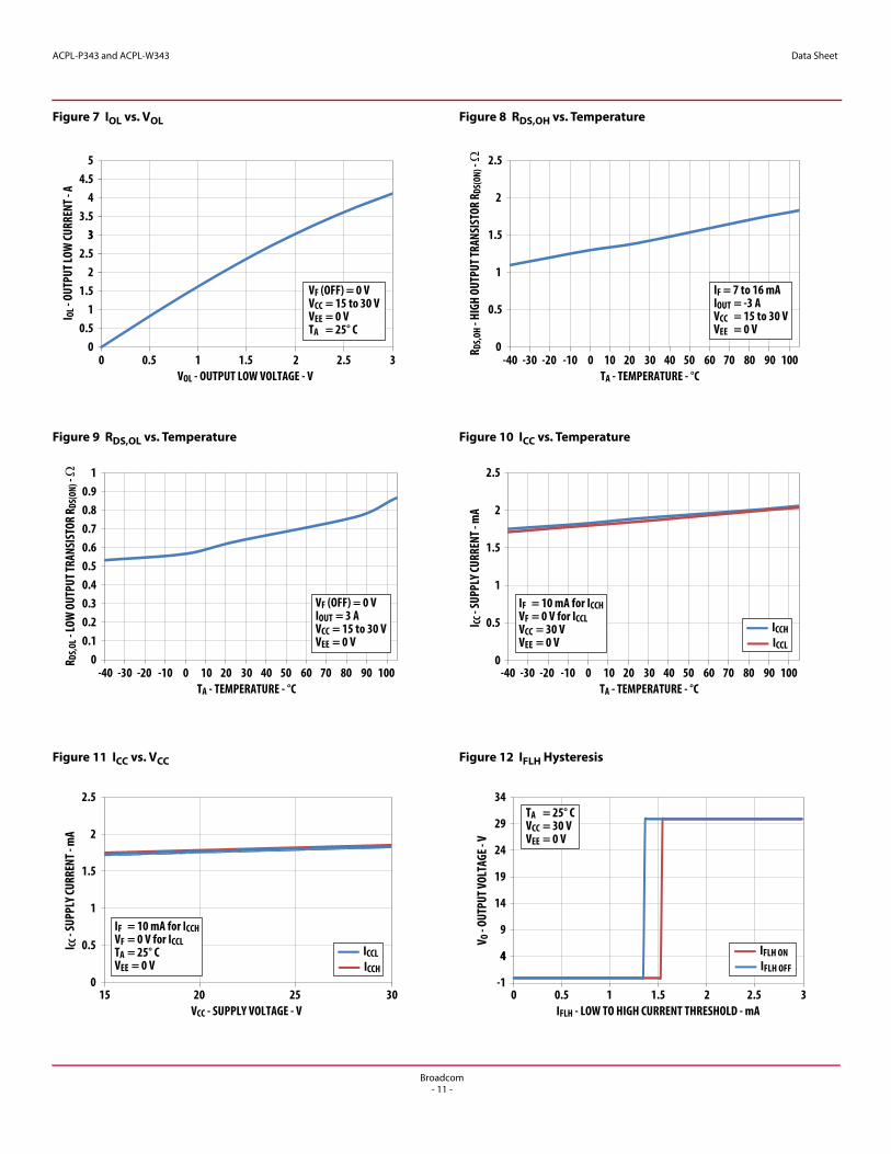
Figure 7 IOL vs. VOL Figure 8 RDS,OH vs. Temperature
33.5
44.5
5
0.51
1.52
2.53
00 0.5 1 1.5 2 32.5
I OL -
OUT
PUT L
OW CU
RREN
T - A
VOL - OUTPUT LOW VOLTAGE - V
VF (OFF) = 0 VVCC = 15 to 30 VVEE = 0 VTA = 25° C
IF = 7 to 16 mAIOUT = -3 AVCC = 15 to 30 VVEE = 0 V
2
2.5
0.5
1
1.5
0R DS,
OH - H
IGH
OUTP
UT TR
ANSI
STOR
RDS
(ON)
-
-40 -30 -20 -10 0 10 20 30 40 50 60 70 80 90 100TA - TEMPERATURE - °C
Figure 9 RDS,OL vs. Temperature Figure 10 ICC vs. Temperature
0.70.80.9
1
0.20.30.40.50.6
00.1
R DS,
OL - L
OW O
UTPU
T TRA
NSIS
TOR
R DS(
ON) -
-40 -30 -20 -10 0 10 20 30 40 50 60 70 80 90 100TA - TEMPERATURE - °C
VF (OFF) = 0 VIOUT = 3 AVCC = 15 to 30 VVEE = 0 V
-40 -30 -20 -10 0 10 20 30 40 50 60 70 80 90 100TA - TEMPERATURE - °C
2
2.5
0.5
1
1.5
I CC - S
UPPL
Y CUR
RENT
- mA
0
IF = 10 mA for ICCHVF = 0 V for ICCLVCC = 30 VVEE = 0 V
ICCHICCL
Figure 11 ICC vs. VCC Figure 12 IFLH Hysteresis
2
2.5
0.5
1
1.5
I CC - S
UPPL
Y CUR
RENT
- mA
015 20 25 30
VCC - SUPPLY VOLTAGE - V
ICCLICCH
IF = 10 mA for ICCHVF = 0 V for ICCLTA = 25° CVEE = 0 V
TA = 25° CVCC = 30 VVEE = 0 V
IFLH ONIFLH OFF
24
29
34
4
9
14
19
V O - O
UTPU
T VOL
TAGE
- V
-1
4
IFLH - LOW TO HIGH CURRENT THRESHOLD - mA0 0.5 1 1.5 2 32.5
Broadcom- 11 -
ACPL-P343 and ACPL-W343 Data Sheet
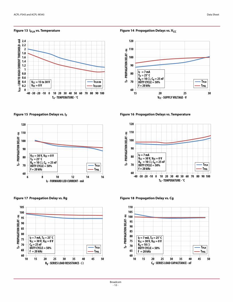
Figure 13 IFLH vs. Temperature Figure 14 Propagation Delays vs. VCC
1.61.8
22.22.4
0.2
0.60.4
0.81
1.21.4
0I FLH -
LOW
TO H
IGH
CURR
ENT T
HRES
HOLD
-mA
-40 -30 -20 -10 0 10 20 30 40 50 60 70 80 90 100TA - TEMPERATURE - °C
VCC = 15 to 30 VVEE = 0 V
IFLH ONIFLH OFF
100
110
120
70
80
90
60
T P - P
ROPA
GATI
ON D
ELAY
- ns
15 20 25 30VCC - SUPPLY VOLTAGE - V
IF = 7 mATA = 25° CRg = 10 , Cg = 25 nFDUTY CYCLE = 50%f = 20 kHz
TPLHTPHL
Figure 15 Propagation Delays vs. IF Figure 16 Propagation Delays vs. Temperature
100
110
120
70
80
90
606 8 10 12 14 16
T P - P
ROPA
GATI
ON D
ELAY
- ns
IF - FORWARD LED CURRENT - mA
VCC = 30 V, VEE = 0 VTA = 25° CRg = 10 , Cg = 25 nFDUTY CYCLE = 50%f = 20 kHz
TPLHTPHL
IF = 7 mAVCC = 30 V, VEE = 0 VRg = 10 , Cg = 25 nFDUTY CYCLE = 50%f = 20 kHz
TPLHTPHL
100
110
120
70
80
90
60
T P - P
ROPA
GATI
ON D
ELAY
- ns
-40 -30 -20 -10 0 10 20 30 40 50 60 70 80 90 100TA - TEMPERATURE - °C
Figure 17 Propagation Delay vs. Rg Figure 18 Propagation Delay vs. Cg
IF = 7 mA, TA = 25° CVCC = 30 V, VEE = 0 VCg = 25 nFDUTY CYCLE = 50%f = 20 kHz
TPLHTPHL
90
95
100
105
65
70
75
80
85
60
65
10 15 20 25 30 35 40 45 50
T P - P
ROPA
GATI
ON D
ELAY
- ns
Rg - SERIES LOAD RESISTANCE -
IF = 7 mA, TA = 25° CVCC = 30 V, VEE = 0 VRg = 10 DUTY CYCLE = 50%f = 20 kHz
TPLHTPHL
10 15 20 25 30 35 40 45 50
95100105110
7075808590
6065
T P - P
ROPA
GATI
ON D
ELAY
- ns
Cg - SERIES LOAD CAPACITANCE - nF
Broadcom- 12 -
ACPL-P343 and ACPL-W343 Data Sheet
Figure 19 Input Current vs. Forward Voltage
Figure 20 IOH Test Circuit
Figure 21 IOL Test Circuit
100
1
10
0.11.4 1.45 1.5 1.55 1.6 1.65
I F - F
ORW
ARD
CURR
ENT -
mA
VF - FORWARD VOLTAGE - V
1 FIF = 7 to 16 mA
1
2
3
6
5
4
+_
+_
4 V Pulsed
VCC = 15 to 30 V
IOH
+_+_
2.5 V Pulsed
VCC = 15 to 30 V1 F
IOL
1
2
3
6
5
4
Broadcom- 13 -
ACPL-P343 and ACPL-W343 Data Sheet
Figure 22 VOH Test Circuit
Figure 23 VOL Test Circuit
Figure 24 IFLH Test Circuit
1
2
3
6
5
4
+_
100 mA
VCC = 15 to 30 V1 FVOH
IF = 7 to 16 mA
100 mA
+_
VCC = 15 to 30 V
VOL
1 F
1
2
3
6
5
4
IF VO > 5 VVCC = 15 to 30 V1 F
10
25 nF
+_
1
2
3
6
5
4
Broadcom- 14 -
ACPL-P343 and ACPL-W343 Data Sheet
Figure 25 UVLO Test Circuit
Figure 26 tPHL, tPHL, tr and tf Test Circuit and Waveforms
Figure 27 CMR Test Circuit with Split Resistors Network and Waveforms
1
2
3
6
5
4
+_
1 FVO > 5 V
IF = 7 to 16 mAVCC
VOVCC = 15 to 30 V1 F
10
25 nF
+_
1
2
3
6
5
4
IF = 7 to 16 mA,20 kHz, 50% Duty Cycle
10 mA
VCC = 30 VVO
+_
1 F
+ _
VCM = 1500 V
5 V
205
137
+_
1
2
3
6
5
4
Broadcom- 15 -
ACPL-P343 and ACPL-W343 Data Sheet
Application Information
Product Overview Description
The ACPL-P343/W343 is an optically isolated power output stage capable of driving IGBTs of up to 200A and 1200V. Based on BCDMOS technology, this gate drive optocoupler delivers higher peak output current, better rail-to-rail output voltage performance and two times faster speed than the previous generation products.
The high peak output current and short propagation delay are needed for fast IGBT switching to reduce dead time and improve system overall efficiency. Rail-to-rail output voltage ensures that the IGBT’s gate voltage is driven to the optimum intended level with no power loss across IGBT. This helps the designer lower the system power which is suitable for bootstrap power supply operation.
It has very high CMR(common mode rejection) rating which allows the microcontroller and the IGBT to operate at very large common mode noise found in industrial motor drives and other power switching applications. The input is driven by direct LED current and has a hysteresis that prevents output oscillation if insufficient LED driving current is applied. This will eliminates the need of additional Schmitt trigger circuit at the input LED.
The stretched SO6 package which is up to 50% smaller than conventional DIP package facilitates smaller more compact design. These stretched packages are compliant to many industrial safety standards, such as IEC/EN/DIN EN 60747-5-5, UL 1577, and CSA.
Recommended Application Circuit
The recommended application circuit shown in Figure 28 illustrates a typical gate drive implementation using the ACPL-P343. The following describes about driving IGBT. However, it is also applicable to MOSFET. Designers will need to adjust the VCC supply voltage, depending on the MOSFET or IGBT gate threshold requirements (recommended VCC = 15V for IGBT and 12V for MOSFET).
The supply bypass capacitors (1 μF) provide the large transient currents necessary during a switching transition. Because of the transient nature of the charging currents, a low current (3.0 mA) power supply will be enough to power the device. The split resistors (in the ratio of 1.5:1) across the LED will provide a high CMR response by providing a balanced resistance network across the LED.
The gate resistor RG serves to limit gate charge current and controls the IGBT collector voltage rise and fall times.
In PC board design, care should be taken to avoid routing the IGBT collector or emitter traces close to the ACPL-P343 input as this can result in unwanted coupling of transient signals into ACPL-P343 and degrade performance.
Figure 28 Recommended Application Circuit with Split Resistors LED Drive
_
VEECATHODE
NC
ANODE
VOUT
VCC
_
R
R
+
1
2
3
6
5
4
Rg +VCE
+ HVDC
-HVDC
3-HVDCAC
1 F
VCC = 15 V
VEE = 5 V
+_
Q1
Q2
_
+VCE_
+_
Broadcom- 16 -

ACPL-P343 and ACPL-W343 Data Sheet
Rail-to-Rail Output
Figure 29 shows a typical gate driver’s high current output stage with 3 bipolar transistors in darlington configuration. During the output high transition, the output voltage rises rapidly to within 3 diode drops of VCC. To ensure the VOUT is at VCC in order to achieve IGBT rated VCE(ON) voltage. The level of VCC will need to be raised to beyond VCC+3(VBE) to account for the diode drops. And to limit the output voltage to VCC, a pull-down resistor, RPULL-DOWN between the output and VEE is recommended to sink a static current while the output is high.
ACPL-P343 uses a power PMOS to deliver the large current and pull it to VCC to achieve rail-to-rail output voltage as shown in Figure 30. This ensures that the IGBT’s gate voltage is driven to the optimum intended level with no power loss across IGBT even when an unstable power supply is used.
Figure 29 Typical Gate Driver with Output Stage in Darlington Confi guration
Figure 30 ACPL-P343/W343 with PMOS and NMOS Output Stage for Rail-to-Rail Output Voltage
1
2
3
4
8
7
6
5
VCC
VOUT
VEE
CATHODE
NC
ANODE
NC
RG
RPULL-DOWN
VCC
VEE
1
2
3
6
5
4CATHODE
NC
ANODE
VOUT
Broadcom- 17 -
ACPL-P343 and ACPL-W343 Data Sheet
Selecting the Gate Resistor (Rg)Step 1: Calculate Rg minimum from the IOL peak specification. The IGBT and Rg in Figure 28 can be analyzed as a simple RC circuit with a voltage supplied by ACPL-P343/W343.
Rg ≥ (VCC – VEE – VOL) / IOLPEAK
= (15V + 5V – 2.9V) / 4A
= 4.3 ≈ 5
The VOL value of 2.9V in the previous equation is the VOL at the peak current of 4.0A (see Figure 7).
Step 2: Check the ACPL-P343/W343 power dissipation and increase Rg if necessary. The ACPL-P343/W343 total power dissipation (PT) is equal to the sum of the emitter power (PE) and the output power (PO).
Using IF(worst case) = 16 mA, Rg = 5, Max Duty Cycle = 80%, Cg = 25 nF, f = 25 kHz and TA max = 85°C:
The value of 3 mA for ICC in the previous equation is the maximum ICC over the entire operating temperature range.
Since PO is less than PO(MAX), Rg = 5 is alright for the power dissipation.
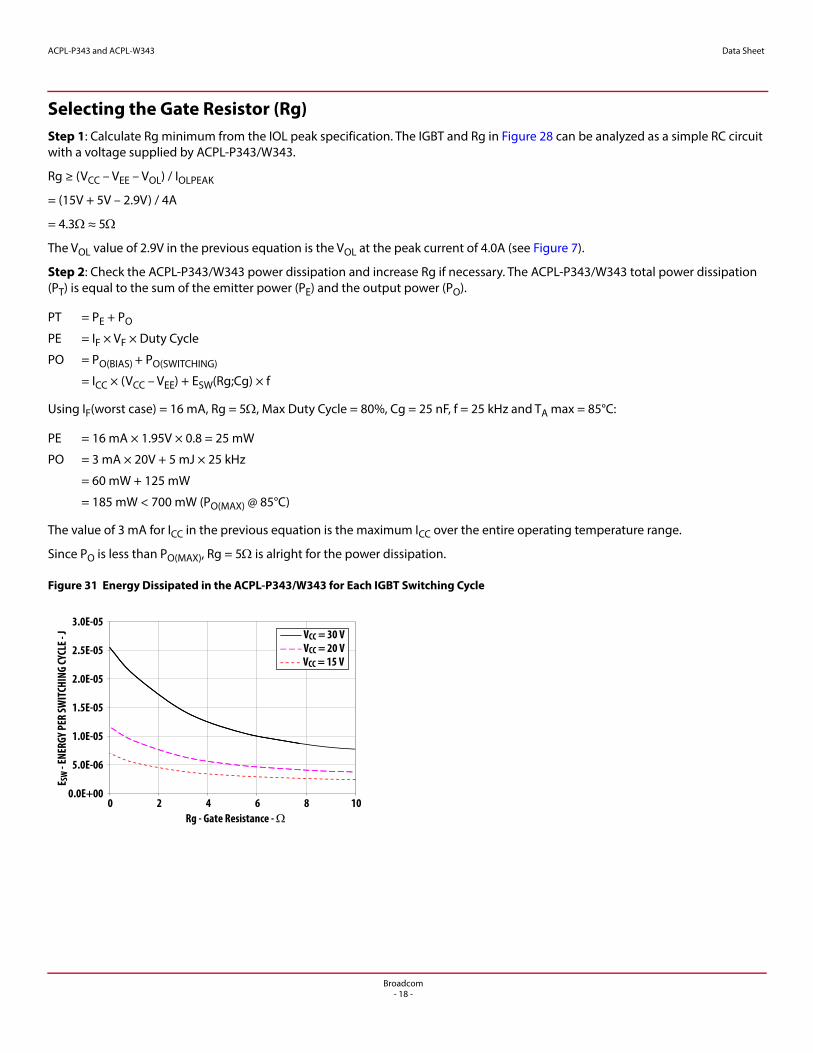
Figure 31 Energy Dissipated in the ACPL-P343/W343 for Each IGBT Switching Cycle
PT = PE + PO
PE = IF × VF × Duty Cycle
PO = PO(BIAS) + PO(SWITCHING)
= ICC × (VCC – VEE) + ESW(Rg;Cg) × f
PE = 16 mA × 1.95V × 0.8 = 25 mW
PO = 3 mA × 20V + 5 mJ × 25 kHz
= 60 mW + 125 mW
= 185 mW < 700 mW (PO(MAX) @ 85°C)
2.0E-05
2.5E-05
3.0E-05
1.0E-05
1.5E-05
0.0E+00
5.0E-06
E SW
- ENE
RGY P
ER SW
ITCH
ING
CYCL
E - J
0 2 4 6 8 10Rg - Gate Resistance -
VCC = 30 VVCC = 20 VVCC = 15 V
Broadcom- 18 -
ACPL-P343 and ACPL-W343 Data Sheet
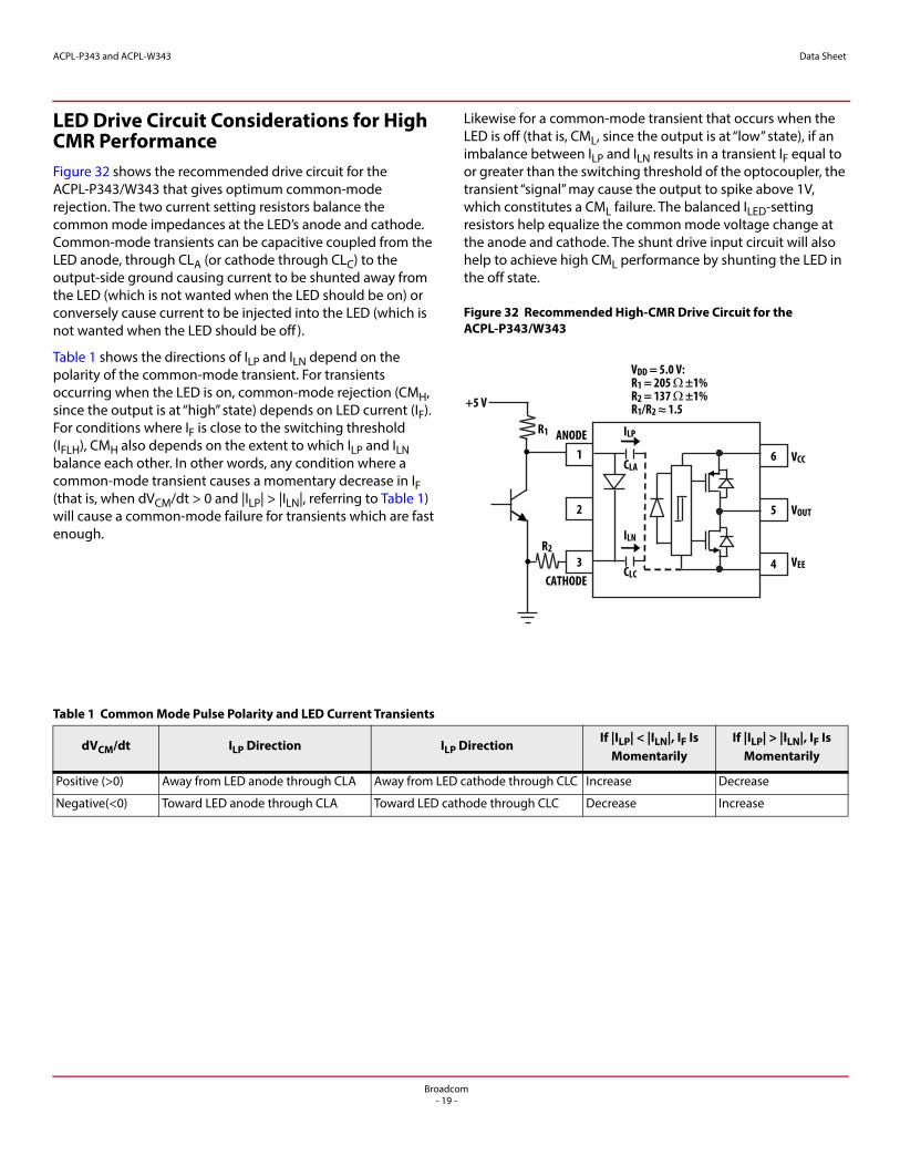
LED Drive Circuit Considerations for High CMR PerformanceFigure 32 shows the recommended drive circuit for the ACPL-P343/W343 that gives optimum common-mode rejection. The two current setting resistors balance the common mode impedances at the LED’s anode and cathode. Common-mode transients can be capacitive coupled from the LED anode, through CLA (or cathode through CLC) to the output-side ground causing current to be shunted away from the LED (which is not wanted when the LED should be on) or conversely cause current to be injected into the LED (which is not wanted when the LED should be off ).
Table 1 shows the directions of ILP and ILN depend on the polarity of the common-mode transient. For transients occurring when the LED is on, common-mode rejection (CMH, since the output is at “high” state) depends on LED current (IF). For conditions where IF is close to the switching threshold (IFLH), CMH also depends on the extent to which ILP and ILN balance each other. In other words, any condition where a common-mode transient causes a momentary decrease in IF (that is, when dVCM/dt > 0 and |ILP| > |ILN|, referring to Table 1) will cause a common-mode failure for transients which are fast enough.
Likewise for a common-mode transient that occurs when the LED is off (that is, CML, since the output is at “low” state), if an imbalance between ILP and ILN results in a transient IF equal to or greater than the switching threshold of the optocoupler, the transient “signal” may cause the output to spike above 1V, which constitutes a CML failure. The balanced ILED-setting resistors help equalize the common mode voltage change at the anode and cathode. The shunt drive input circuit will also help to achieve high CML performance by shunting the LED in the off state.
Figure 32 Recommended High-CMR Drive Circuit for the ACPL-P343/W343
+5 V
R1
R2
VCC
VEE
1
2
3
6
5
4CATHODE
ANODE
VOUT
ILP
ILN
CLA
CLC
VDD = 5.0 V:R1 = 205 ±1%R2 = 137 ±1%R1/R2 ≈ 1.5
Table 1 Common Mode Pulse Polarity and LED Current Transients
dVCM/dt ILP Direction ILP Direction If |ILP| < |ILN|, IF Is Momentarily
If |ILP| > |ILN|, IF Is Momentarily
Positive (>0) Away from LED anode through CLA Away from LED cathode through CLC Increase Decrease
Negative(<0) Toward LED anode through CLA Toward LED cathode through CLC Decrease Increase
Broadcom- 19 -

ACPL-P343 and ACPL-W343 Data Sheet
Dead Time and Propagation Delay SpecificationsThe ACPL-P343/W343 includes a Propagation Delay Difference (PDD) specification intended to help designers minimize “dead time” in their power inverter designs. Dead time is the time period during which both the high and low side power transistors (Q1 and Q2 in Figure 28) are off. Any overlap in Q1 and Q2 conduction will result in large currents flowing through the power devices between the high and low voltage motor rails.
To minimize dead time in a given design, the turn on of LED2 should be delayed (relative to the turn off of LED1) so that under worst-case conditions, transistor Q1 has just turned off when transistor Q2 turns on, as shown in Figure 33. The amount of delay necessary to achieve this condition is equal to the maximum value of the propagation delay difference specification, PDDMAX, which is specified to be 100 ns over the operating temperature range of 40°C to 105°C.
Figure 33 Minimum LED Skew for Zero Dead Time
Delaying the LED signal by the maximum propagation delay difference ensures that the minimum dead time is zero, but it does not tell a designer what the maximum dead time will be. The maximum dead time is equivalent to the difference between the maximum and minimum propagation delay difference specifications as shown in Figure 34. The maximum dead time for the ACPL-P343/W343 is 200 ns (= 100 ns – (–100 ns)) over an operating temperature range of –40°C to 105°C.
Note that the propagation delays used to calculate PDD and dead time are taken at equal temperatures and test conditions since the optocouplers under consideration are typically mounted in close proximity to each other and are switching identical IGBTs.
Figure 34 Waveforms for Dead Time
tPHL MAX
tPLH MIN
PDD* MAX = (tPHL - tPLH) MAX = tPHL MAX - tPLH MIN
*PDD = Propagation Delay DifferenceNote: for PDD calculations the propagation delaysAre taken at the same temperature and test conditions.
VOUT1
ILED2
VOUT2
ILED1
Q1 ON
Q2 OFF
Q1 OFF
Q2 ONtPLH MIN
MAXIMUM DEAD TIME(DUE TO OPTOCOUPLER)= (tPHL MAX - tPHL MIN) + (tPLH MAX - tPLH MIN)= (tPHL MAX - tPLH MIN) + (tPHL MIN - tPLH MAX)= PDD* MAX - PDD* MIN
Q1 ON
Q2 OFF
Q1 OFF
Q2 ON
tPLH MINtPHL MAX
tPLH MAX
PDD* MAX
*PDD = Propagation Delay DifferenceNote: For Dead Time and PDD calculations all propagation delays are taken at the same temperature and test conditions.
VOUT1
ILED2
VOUT2
ILED1
(tPHL - tPLH) MAX
Broadcom- 20 -
ACPL-P343 and ACPL-W343 Data Sheet
LED Current Input with HysteresisThe detector has optical receiver input stage with built in Schmitt trigger to provide logic compatible waveforms, eliminating the need for additional wave shaping. The hysteresis (Figure 12) provides differential mode noise immunity and minimizes the potential for output signal chatter.
Under Voltage LockoutThe ACPL-P343/W343 Under Voltage Lockout (UVLO) feature is designed to prevent the application of insufficient gate voltage to the IGBT by forcing the ACPL-P343/W343 output low during power-up. IGBTs typically require gate voltages of 15V to achieve their rated VCE(ON) voltage. At gate voltages below 13V typically, the VCE(ON) voltage increases dramatically, especially at higher currents. At very low gate voltages (below 10V), the IGBT may operate in the linear region and quickly overheat. The UVLO function causes the output to be clamped whenever insufficient operating supply (VCC) is applied. Once VCC exceeds VUVLO+ (the positive-going UVLO threshold), the UVLO clamp is released to allow the device output to turn on in response to input signals.
Thermal Model for ACPL-P343/W343 Stretched SO6 Package Optocoupler
Definitions:
R11: Junction to ambient thermal resistance of LED due to heating of LED.
R12: Junction to ambient thermal resistance of LED due to heating of detector (output IC).
R21: Junction to ambient thermal resistance of detector (output IC) due to heating of LED.
R22: Junction to ambient thermal resistance of detector (output IC) due to heating of detector (output IC).
P1: Power dissipation of LED (W).
P2: Power dissipation of detector/output IC (W).
T1: Junction temperature of LED (°C).
T2: Junction temperature of detector (°C).
Ta: Ambient temperature.
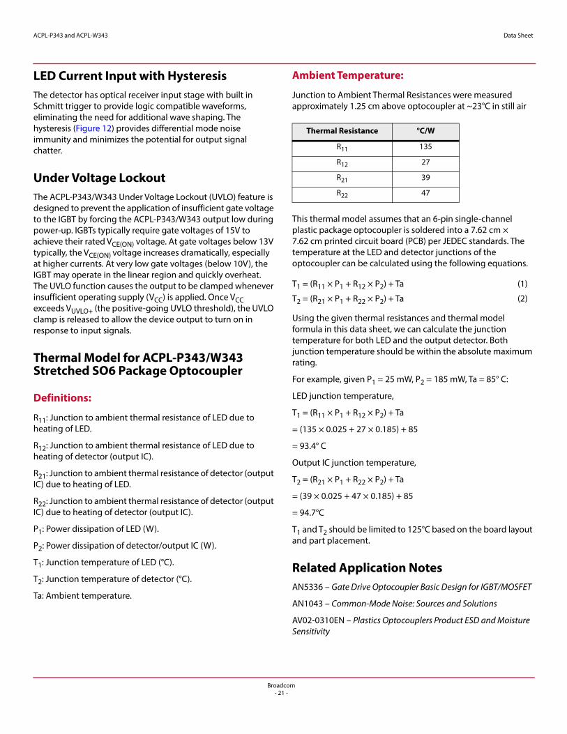
Ambient Temperature:
Junction to Ambient Thermal Resistances were measured approximately 1.25 cm above optocoupler at ~23°C in still air
This thermal model assumes that an 6-pin single-channel plastic package optocoupler is soldered into a 7.62 cm × 7.62 cm printed circuit board (PCB) per JEDEC standards. The temperature at the LED and detector junctions of the optocoupler can be calculated using the following equations.
Using the given thermal resistances and thermal model formula in this data sheet, we can calculate the junction temperature for both LED and the output detector. Both junction temperature should be within the absolute maximum rating.
For example, given P1 = 25 mW, P2 = 185 mW, Ta = 85° C:
LED junction temperature,
T1 = (R11 × P1 + R12 × P2) + Ta
= (135 × 0.025 + 27 × 0.185) + 85
= 93.4° C
Output IC junction temperature,
T2 = (R21 × P1 + R22 × P2) + Ta
= (39 × 0.025 + 47 × 0.185) + 85
= 94.7°C
T1 and T2 should be limited to 125°C based on the board layout and part placement.
Related Application NotesAN5336 – Gate Drive Optocoupler Basic Design for IGBT/MOSFET
AN1043 – Common-Mode Noise: Sources and Solutions
AV02-0310EN – Plastics Optocouplers Product ESD and Moisture Sensitivity
Thermal Resistance °C/W
R11 135
R12 27
R21 39
R22 47
T1 = (R11 × P1 + R12 × P2) + Ta (1)
T2 = (R21 × P1 + R22 × P2) + Ta (2)
Broadcom- 21 -

For product information and a complete list of distributors, please go to our web site: www.broadcom.com.
Broadcom, the pulse logo, Connecting everything, Avago Technologies, Avago, and the A logo are among the trademarks of Broadcom and/or its affiliates in the United States, certain other countries and/or the EU.
Copyright © 2011–2017 by Broadcom. All Rights Reserved.
The term "Broadcom" refers to Broadcom Limited and/or its subsidiaries. For more information, please visit www.broadcom.com.
Broadcom reserves the right to make changes without further notice to any products or data herein to improve reliability, function, or design.
Information furnished by Broadcom is believed to be accurate and reliable. However, Broadcom does not assume any liability arising out of the application or use of this information, nor the application or use of any product or circuit described herein, neither does it convey any license under its patent rights nor the rights of others.
AV02-2928EN – April 28, 2017