acpl-k43t, acpl-k44t: automotive r2coupler wide operating
TRANSCRIPT
Data Sheet
ACPL-K43T, ACPL-K44TAutomotive R2Coupler™ Wide Operating Temperature 1-MBd Digital Optocoupler in a Stretched 8-Pin Surface-Mount Plastic Package
Description
The Broadcom® ACPL-K43T is a single-channel, high-temperature, high-CMR, high-speed digital optocoupler in an eight-lead miniature footprint specifically used in the automotive applications. The ACPL-K44T is a dual-channel equivalent of the ACPL-K43T. Both products are available in the stretched SO-8 package outline designed to be compatible with standard surface-mount processes.
This digital optocoupler uses an insulating layer between the light-emitting diode and an integrated photo detector to provide electrical insulation between input and output. Separate connections for the photodiode bias and output transistor collector increase the speed up to a hundred times over that of a conventional photo-transistor coupler by reducing the base-collector capacitance.
Broadcom R2Coupler™ isolation products provide with reinforced insulation and reliability that deliver safe signal isolation, which is critical in automotive and high-temperature industrial applications.
Features
High temperature and reliability low-speed digital interface for automotive applications
Ultra-low drive for status feedback at IF = 0.8 mA or 1.5 mA
30 kV/µs (typ.) high common-mode rejection at VCM = 1500V
Compact, auto-insertable stretched SO8 packages
Qualified to AEC Q100 Grade 1 test guidelines
Wide operating temperature range: –40°C to +125°C
High speed: 1 MBd
Low propagation delay: 1 µs max. at IF = 10 mA
Worldwide safety approval:
– UL 1577 approval, 5 kVRMS/1 min.
– CSA approval
– IEC/EN/DIN EN 60747-5-5
Applications Automotive IPM driver for DC-DC converters and motor
inverters
Status feedback and wake-up signal isolation
CANBus and SPI communications interface
High-temperature digital/analog signal isolation
CAUTION! Take normal static precautions in handling and assembly of this component to prevent damage, degradation, or both, which may be induced by ESD.
Broadcom AV02-3179ENSeptember 26, 2018
ACPL-K43T, ACPL-K44T Data Sheet Automotive R2Coupler™ Wide Operating Temperature 1-MBd Digital Optocoupler in a
Stretched 8-Pin Surface-Mount Plastic Package
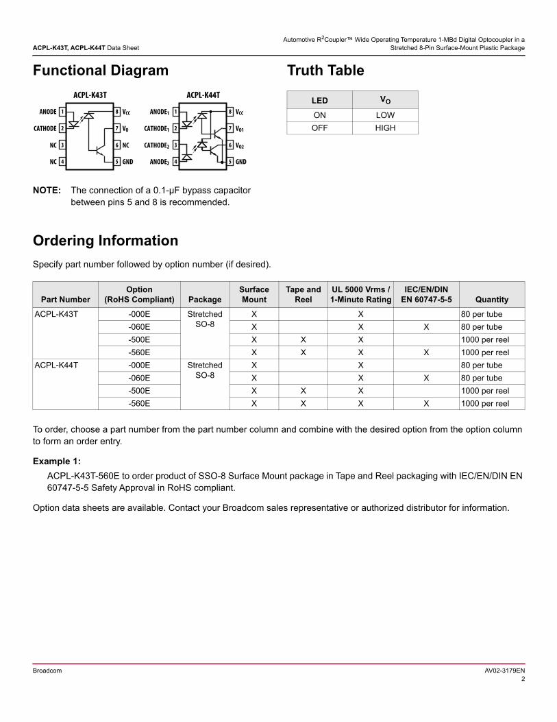
Functional Diagram
NOTE: The connection of a 0.1-µF bypass capacitor between pins 5 and 8 is recommended.
Truth Table
7
1
2
3
4 5
6
8ANODE
CATHODE
NC
NC
VCC
VO
NC
GND
ACPL-K43T
7
1
2
3
4 5
6
8ANODE1
CATHODE1
CATHODE2
ANODE2
VCC
VO1
VO2
GND
ACPL-K44TLED VO
ON LOW
OFF HIGH
Ordering Information
Specify part number followed by option number (if desired).
To order, choose a part number from the part number column and combine with the desired option from the option column to form an order entry.
Example 1:
ACPL-K43T-560E to order product of SSO-8 Surface Mount package in Tape and Reel packaging with IEC/EN/DIN EN 60747-5-5 Safety Approval in RoHS compliant.
Option data sheets are available. Contact your Broadcom sales representative or authorized distributor for information.
Part NumberOption
(RoHS Compliant) PackageSurface Mount
Tape and Reel
UL 5000 Vrms /1-Minute Rating
IEC/EN/DIN EN 60747-5-5 Quantity
ACPL-K43T -000E Stretched SO-8
X X 80 per tube
-060E X X X 80 per tube
-500E X X X 1000 per reel
-560E X X X X 1000 per reel
ACPL-K44T -000E Stretched SO-8
X X 80 per tube
-060E X X X 80 per tube
-500E X X X 1000 per reel
-560E X X X X 1000 per reel
Broadcom AV02-3179EN2
ACPL-K43T, ACPL-K44T Data Sheet Automotive R2Coupler™ Wide Operating Temperature 1-MBd Digital Optocoupler in a
Stretched 8-Pin Surface-Mount Plastic Package
Schematic
ACPL-K43T
IF
SHIELD
8
7
VCC
1
2
VO
VCC
VO1
ICC
VF IO
ANODE
CATHODE
+
–
5GND
ACPL-K44T
8
7
1
2
VF1 IO1
+
–
IF1ICC
3
4
VF2
IO2VO2
6
–
+
IF2
GND5
USE OF 0.1 F BYPASS CAPACITOR CONNECTEDBETWEEN PINS 5 AND 8 IS RECOMMENDED.
Broadcom AV02-3179EN3
ACPL-K43T, ACPL-K44T Data Sheet Automotive R2Coupler™ Wide Operating Temperature 1-MBd Digital Optocoupler in a
Stretched 8-Pin Surface-Mount Plastic Package
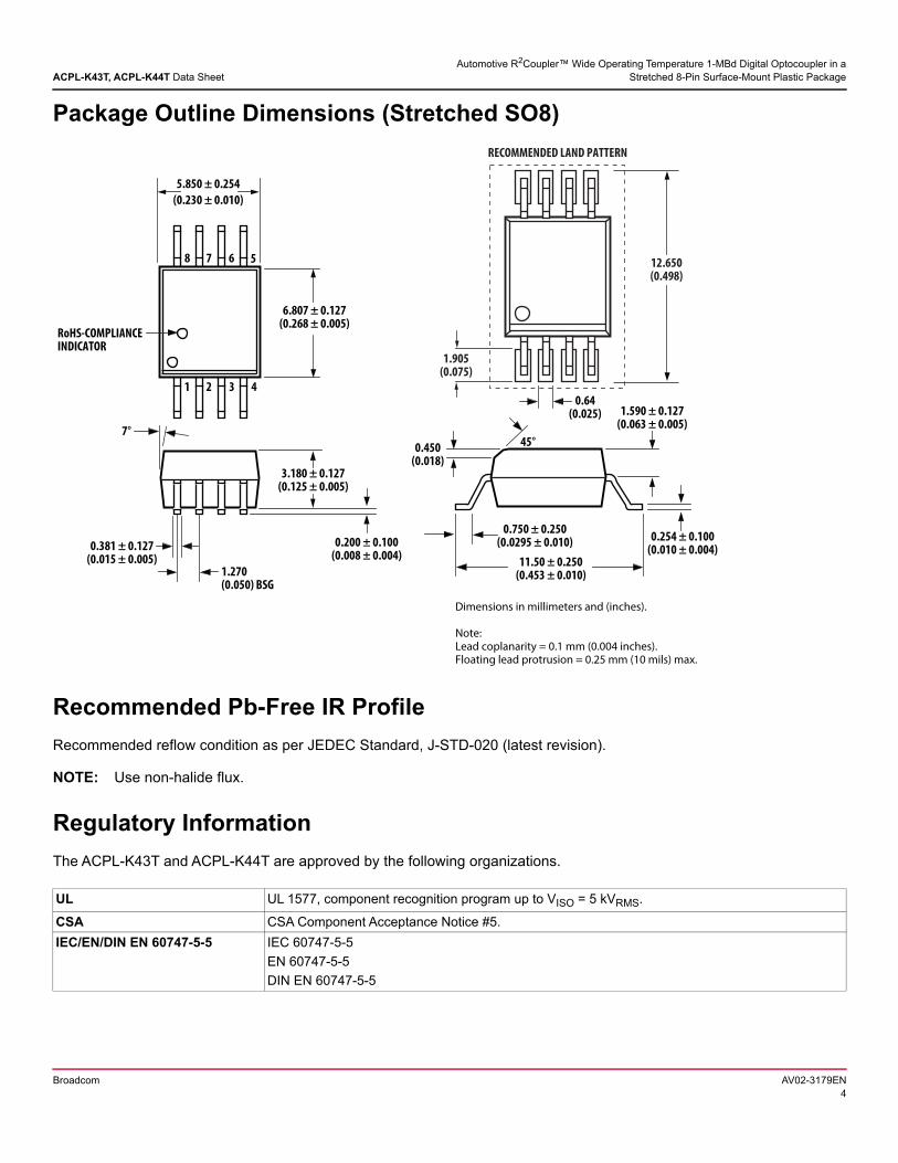
Package Outline Dimensions (Stretched SO8)
Recommended Pb-Free IR Profile
Recommended reflow condition as per JEDEC Standard, J-STD-020 (latest revision).
NOTE: Use non-halide flux.
Regulatory Information
The ACPL-K43T and ACPL-K44T are approved by the following organizations.
UL UL 1577, component recognition program up to VISO = 5 kVRMS.
CSA CSA Component Acceptance Notice #5.
IEC/EN/DIN EN 60747-5-5 IEC 60747-5-5
EN 60747-5-5
DIN EN 60747-5-5
5.850 ± 0.254
(0.230 ± 0.010)
5678
4321
Dimensions in millimeters and (inches).
Note:Lead coplanarity = 0.1 mm (0.004 inches).Floating lead protrusion = 0.25 mm (10 mils) max.
6.807 ± 0.127(0.268 ± 0.005)
RECOMMENDED LAND PATTERN
12.650(0.498)
1.905(0.075)
3.180 ± 0.127 (0.125 ± 0.005)
0.381 ± 0.127(0.015 ± 0.005)
1.270(0.050) BSG
7°
0.254 ± 0.100(0.010 ± 0.004)
0.750 ± 0.250(0.0295 ± 0.010)
11.50 ± 0.250(0.453 ± 0.010)
1.590 ± 0.127(0.063 ± 0.005)
0.450(0.018)
45°
RoHS-COMPLIANCEINDICATOR
0.64(0.025)
0.200 ± 0.100(0.008 ± 0.004)
Broadcom AV02-3179EN4
ACPL-K43T, ACPL-K44T Data Sheet Automotive R2Coupler™ Wide Operating Temperature 1-MBd Digital Optocoupler in a
Stretched 8-Pin Surface-Mount Plastic Package
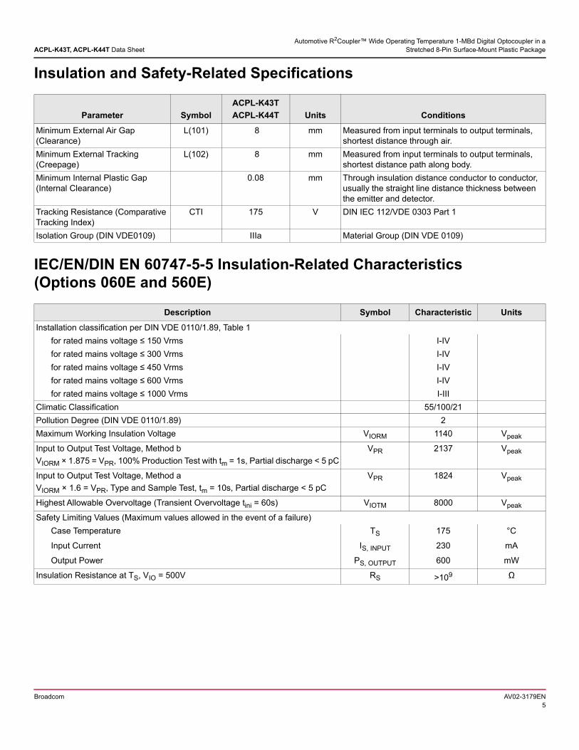
Insulation and Safety-Related Specifications
IEC/EN/DIN EN 60747-5-5 Insulation-Related Characteristics (Options 060E and 560E)
Parameter Symbol
ACPL-K43T
ACPL-K44T Units Conditions
Minimum External Air Gap (Clearance)
L(101) 8 mm Measured from input terminals to output terminals, shortest distance through air.
Minimum External Tracking (Creepage)
L(102) 8 mm Measured from input terminals to output terminals, shortest distance path along body.
Minimum Internal Plastic Gap (Internal Clearance)
0.08 mm Through insulation distance conductor to conductor, usually the straight line distance thickness between the emitter and detector.
Tracking Resistance (Comparative Tracking Index)
CTI 175 V DIN IEC 112/VDE 0303 Part 1
Isolation Group (DIN VDE0109) IIIa Material Group (DIN VDE 0109)
Description Symbol Characteristic Units
Installation classification per DIN VDE 0110/1.89, Table 1
for rated mains voltage ≤ 150 Vrms I-IV
for rated mains voltage ≤ 300 Vrms I-IV
for rated mains voltage ≤ 450 Vrms I-IV
for rated mains voltage ≤ 600 Vrms I-IV
for rated mains voltage ≤ 1000 Vrms I-III
Climatic Classification 55/100/21
Pollution Degree (DIN VDE 0110/1.89) 2
Maximum Working Insulation Voltage VIORM 1140 Vpeak
Input to Output Test Voltage, Method b
VIORM × 1.875 = VPR, 100% Production Test with tm = 1s, Partial discharge < 5 pC
VPR 2137 Vpeak
Input to Output Test Voltage, Method a
VIORM × 1.6 = VPR, Type and Sample Test, tm = 10s, Partial discharge < 5 pC
VPR 1824 Vpeak
Highest Allowable Overvoltage (Transient Overvoltage tini = 60s) VIOTM 8000 Vpeak
Safety Limiting Values (Maximum values allowed in the event of a failure)
Case Temperature TS 175 °C
Input Current IS, INPUT 230 mA
Output Power PS, OUTPUT 600 mW
Insulation Resistance at TS, VIO = 500V RS >109 Ω
Broadcom AV02-3179EN5
ACPL-K43T, ACPL-K44T Data Sheet Automotive R2Coupler™ Wide Operating Temperature 1-MBd Digital Optocoupler in a
Stretched 8-Pin Surface-Mount Plastic Package
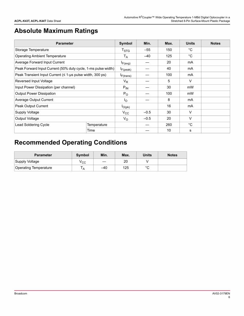
Absolute Maximum Ratings
Recommended Operating Conditions
Parameter Symbol Min. Max. Units Notes
Storage Temperature TSTG –55 150 °C
Operating Ambient Temperature TA –40 125 °C
Average Forward Input Current IF(avg) — 20 mA
Peak Forward Input Current (50% duty cycle, 1-ms pulse width) IF(peak) — 40 mA
Peak Transient Input Current (≤ 1-µs pulse width, 300 ps) IF(trans) — 100 mA
Reversed Input Voltage VR — 5 V
Input Power Dissipation (per channel) PIN — 30 mW
Output Power Dissipation PO — 100 mW
Average Output Current IO — 8 mA
Peak Output Current IO(pk) 16 mA
Supply Voltage VCC –0.5 30 V
Output Voltage VO –0.5 20 V
Lead Soldering Cycle Temperature — 260 °C
Time — 10 s
Parameter Symbol Min. Max. Units Notes
Supply Voltage VCC — 20 V
Operating Temperature TA –40 125 °C
Broadcom AV02-3179EN6
ACPL-K43T, ACPL-K44T Data Sheet Automotive R2Coupler™ Wide Operating Temperature 1-MBd Digital Optocoupler in a
Stretched 8-Pin Surface-Mount Plastic Package
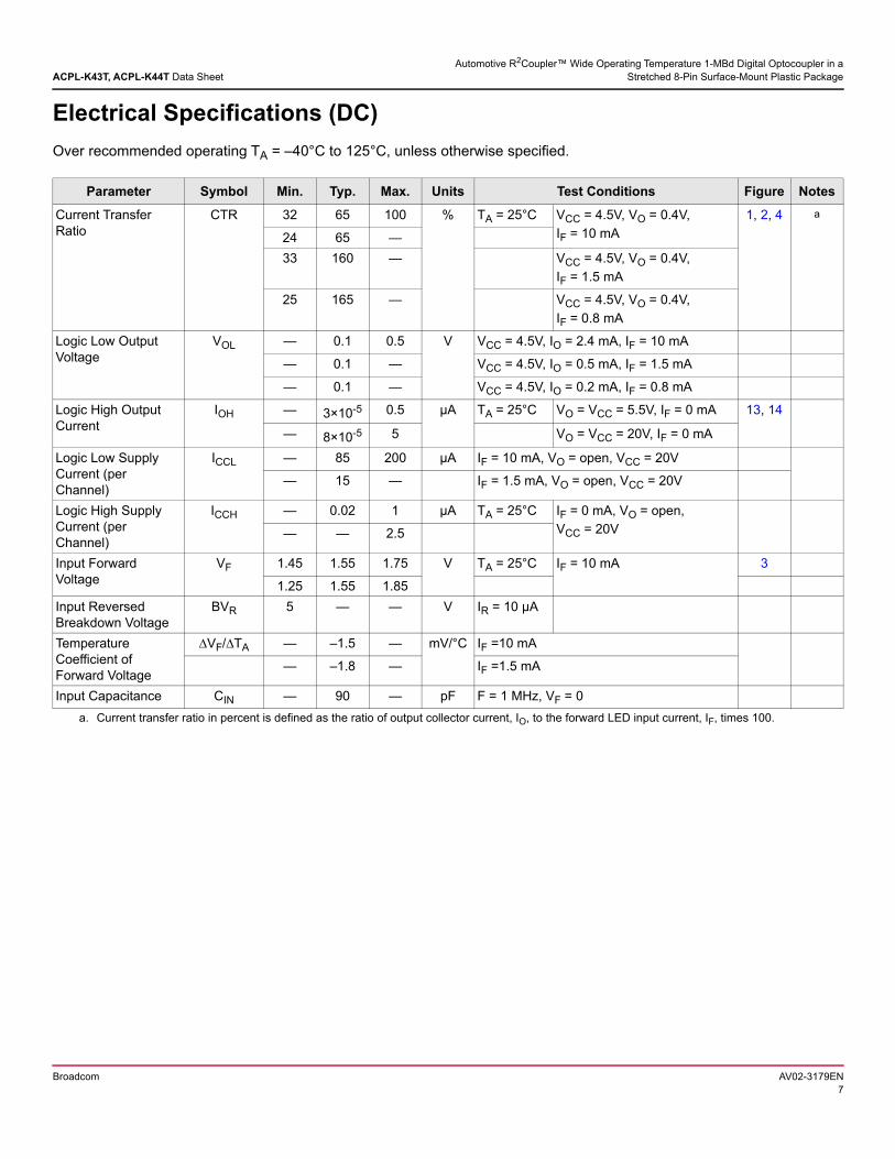
Electrical Specifications (DC)
Over recommended operating TA = –40°C to 125°C, unless otherwise specified.
Parameter Symbol Min. Typ. Max. Units Test Conditions Figure Notes
Current Transfer Ratio
CTR 32 65 100 % TA = 25°C VCC = 4.5V, VO = 0.4V,
IF = 10 mA
1, 2, 4 a
a. Current transfer ratio in percent is defined as the ratio of output collector current, IO, to the forward LED input current, IF, times 100.
24 65 —
33 160 — VCC = 4.5V, VO = 0.4V,
IF = 1.5 mA
25 165 — VCC = 4.5V, VO = 0.4V,
IF = 0.8 mA
Logic Low Output Voltage
VOL — 0.1 0.5 V VCC = 4.5V, IO = 2.4 mA, IF = 10 mA
— 0.1 — VCC = 4.5V, IO = 0.5 mA, IF = 1.5 mA
— 0.1 — VCC = 4.5V, IO = 0.2 mA, IF = 0.8 mA
Logic High Output Current
IOH — 3×10⁻⁵ 0.5 µA TA = 25°C VO = VCC = 5.5V, IF = 0 mA 13, 14
— 8×10⁻⁵ 5 VO = VCC = 20V, IF = 0 mA
Logic Low Supply Current (per Channel)
ICCL — 85 200 µA IF = 10 mA, VO = open, VCC = 20V
— 15 — IF = 1.5 mA, VO = open, VCC = 20V
Logic High Supply Current (per Channel)
ICCH — 0.02 1 µA TA = 25°C IF = 0 mA, VO = open,
VCC = 20V— — 2.5
Input Forward Voltage
VF 1.45 1.55 1.75 V TA = 25°C IF = 10 mA 3
1.25 1.55 1.85
Input Reversed Breakdown Voltage
BVR 5 — — V IR = 10 µA
Temperature Coefficient of Forward Voltage
∆VF/∆TA — –1.5 — mV/°C IF =10 mA
— –1.8 — IF =1.5 mA
Input Capacitance CIN — 90 — pF F = 1 MHz, VF = 0
Broadcom AV02-3179EN7
ACPL-K43T, ACPL-K44T Data Sheet Automotive R2Coupler™ Wide Operating Temperature 1-MBd Digital Optocoupler in a
Stretched 8-Pin Surface-Mount Plastic Package
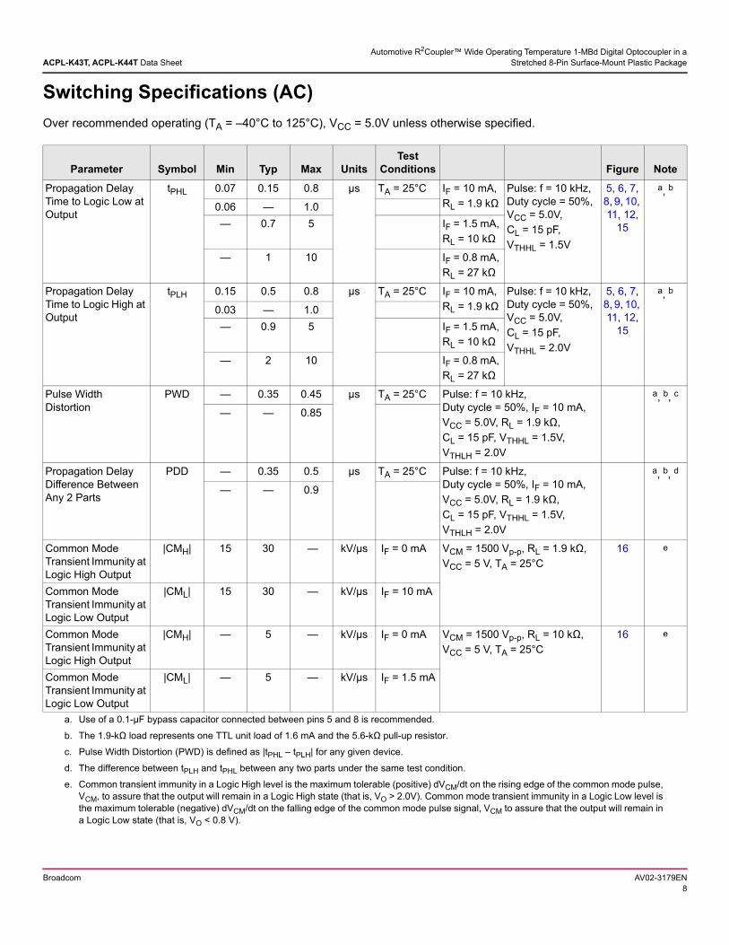
Switching Specifications (AC)
Over recommended operating (TA = –40°C to 125°C), VCC = 5.0V unless otherwise specified.
Parameter Symbol Min Typ Max UnitsTest
Conditions Figure Note
Propagation Delay Time to Logic Low at Output
tPHL 0.07 0.15 0.8 µs TA = 25°C IF = 10 mA,
RL = 1.9 kΩ
Pulse: f = 10 kHz, Duty cycle = 50%, VCC = 5.0V,
CL = 15 pF,
VTHHL = 1.5V
5, 6, 7, 8, 9, 10, 11, 12,
15
a, b
a. Use of a 0.1-µF bypass capacitor connected between pins 5 and 8 is recommended.
b. The 1.9-kΩ load represents one TTL unit load of 1.6 mA and the 5.6-kΩ pull-up resistor.
0.06 — 1.0
— 0.7 5 IF = 1.5 mA,
RL = 10 kΩ
— 1 10 IF = 0.8 mA,
RL = 27 kΩ
Propagation Delay Time to Logic High at Output
tPLH 0.15 0.5 0.8 µs TA = 25°C IF = 10 mA,
RL = 1.9 kΩ
Pulse: f = 10 kHz, Duty cycle = 50%, VCC = 5.0V,
CL = 15 pF,
VTHHL = 2.0V
5, 6, 7, 8, 9, 10, 11, 12,
15
a, b
0.03 — 1.0
— 0.9 5 IF = 1.5 mA,
RL = 10 kΩ
— 2 10 IF = 0.8 mA,
RL = 27 kΩ
Pulse Width Distortion
PWD — 0.35 0.45 µs TA = 25°C Pulse: f = 10 kHz, Duty cycle = 50%, IF = 10 mA,
VCC = 5.0V, RL = 1.9 kΩ,
CL = 15 pF, VTHHL = 1.5V,
VTHLH = 2.0V
a, b, c
c. Pulse Width Distortion (PWD) is defined as |tPHL – tPLH| for any given device.
— — 0.85
Propagation Delay Difference Between Any 2 Parts
PDD — 0.35 0.5 µs TA = 25°C Pulse: f = 10 kHz, Duty cycle = 50%, IF = 10 mA,
VCC = 5.0V, RL = 1.9 kΩ,
CL = 15 pF, VTHHL = 1.5V,
VTHLH = 2.0V
a, b, d
d. The difference between tPLH and tPHL between any two parts under the same test condition.
— — 0.9
Common Mode Transient Immunity at Logic High Output
|CMH| 15 30 — kV/µs IF = 0 mA VCM = 1500 Vp-p, RL = 1.9 kΩ,
VCC = 5 V, TA = 25°C
16 e
e. Common transient immunity in a Logic High level is the maximum tolerable (positive) dVCM/dt on the rising edge of the common mode pulse, VCM, to assure that the output will remain in a Logic High state (that is, VO > 2.0V). Common mode transient immunity in a Logic Low level is the maximum tolerable (negative) dVCM/dt on the falling edge of the common mode pulse signal, VCM to assure that the output will remain in a Logic Low state (that is, VO < 0.8 V).
Common Mode Transient Immunity at Logic Low Output
|CML| 15 30 — kV/µs IF = 10 mA
Common Mode Transient Immunity at Logic High Output
|CMH| — 5 — kV/µs IF = 0 mA VCM = 1500 Vp-p, RL = 10 kΩ,
VCC = 5 V, TA = 25°C
16 e
Common Mode Transient Immunity at Logic Low Output
|CML| — 5 — kV/µs IF = 1.5 mA
Broadcom AV02-3179EN8
ACPL-K43T, ACPL-K44T Data Sheet Automotive R2Coupler™ Wide Operating Temperature 1-MBd Digital Optocoupler in a
Stretched 8-Pin Surface-Mount Plastic Package
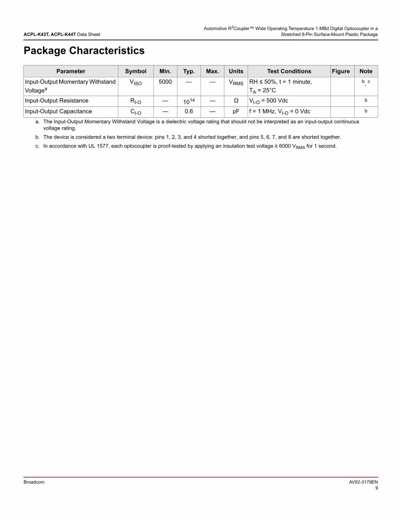
Package Characteristics
Parameter Symbol Min. Typ. Max. Units Test Conditions Figure Note
Input-Output Momentary Withstand
Voltagea
a. The Input-Output Momentary Withstand Voltage is a dielectric voltage rating that should not be interpreted as an input-output continuous voltage rating.
VISO 5000 — — VRMS RH ≤ 50%, t = 1 minute,
TA = 25°C
b, c
b. The device is considered a two terminal device: pins 1, 2, 3, and 4 shorted together, and pins 5, 6, 7, and 8 are shorted together.
c. In accordance with UL 1577, each optocoupler is proof-tested by applying an insulation test voltage ≥ 6000 VRMS for 1 second.
Input-Output Resistance RI-O — 1014 — Ω VI-O = 500 Vdc b
Input-Output Capacitance CI-O — 0.6 — pF f = 1 MHz, VI-O = 0 Vdc b
Broadcom AV02-3179EN9
ACPL-K43T, ACPL-K44T Data Sheet Automotive R2Coupler™ Wide Operating Temperature 1-MBd Digital Optocoupler in a
Stretched 8-Pin Surface-Mount Plastic Package
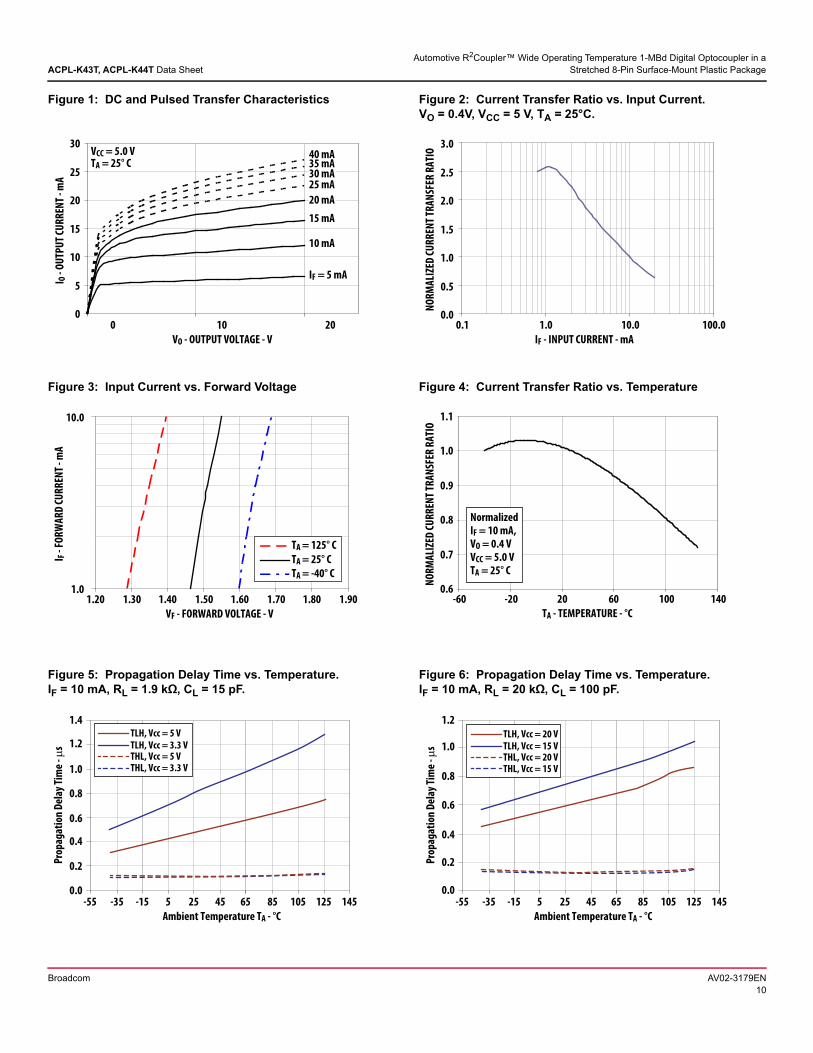
Figure 1: DC and Pulsed Transfer Characteristics Figure 2: Current Transfer Ratio vs. Input Current. VO = 0.4V, VCC = 5 V, TA = 25°C.
0
5
10
15
20
25
30
0 10 20
VO - OUTPUT VOLTAGE - V
I O -
OU
TPU
T CU
RR
ENT
- mA
VCC = 5.0 VTA = 25° C
40 mA35 mA
25 mA
15 mA
10 mA
IF = 5 mA
20 mA
30 mA
0.0
0.5
1.0
1.5
2.0
2.5
3.0
0.1 1.0 10.0 100.0
IF - INPUT CURRENT - mA
NO
RM
ALI
ZED
CU
RR
ENT
TRA
NSF
ER R
ATI
O
Figure 3: Input Current vs. Forward Voltage Figure 4: Current Transfer Ratio vs. Temperature
1.0
10.0
1.20 1.30 1.40 1.50 1.60 1.70 1.80 1.90
VF - FORWARD VOLTAGE - V
I F -
FOR
WA
RD
CU
RR
ENT
- mA
TA = 125° C
TA = 25° C
TA = -40° C
0.6
0.7
0.8
0.9
1.0
1.1
-60 -20 20 60 100 140
NO
RM
ALI
ZED
CU
RR
ENT
TRA
NSF
ER R
ATI
O
TA - TEMPERATURE - °C
NormalizedIF = 10 mA,VO = 0.4 VVCC = 5.0 VTA = 25° C
Figure 5: Propagation Delay Time vs. Temperature.IF = 10 mA, RL = 1.9 kΩ, CL = 15 pF.
Figure 6: Propagation Delay Time vs. Temperature. IF = 10 mA, RL = 20 kΩ, CL = 100 pF.
0.0
0.2
0.4
0.6
0.8
1.0
1.2
1.4
-55 -15-35 5 25 45 65 85 105 125 145
Ambient Temperature TA - °C
Pro
paga
tion
Del
ay T
ime
- s
THL, Vcc = 5 V
TLH, Vcc = 5 V
THL, Vcc = 3.3 V
TLH, Vcc = 3.3 V
0.2
0.0
0.4
0.6
0.8
1.0
1.2
-55 -15-35 5 25 45 65 85 105 125 145
Ambient Temperature TA - °C
Pro
paga
tion
Del
ay T
ime
- s
THL, Vcc = 20 V
TLH, Vcc = 20 V
THL, Vcc = 15 V
TLH, Vcc = 15 V
Broadcom AV02-3179EN10
ACPL-K43T, ACPL-K44T Data Sheet Automotive R2Coupler™ Wide Operating Temperature 1-MBd Digital Optocoupler in a
Stretched 8-Pin Surface-Mount Plastic Package
Figure 7: Propagation Delay Time vs. Load Resistance Figure 8: Propagation Delay Time vs. Load Resistance
0.0
0.5
1.0
1.5
2.0
2.5
3.0
1 2 3 4 5 6 7 8 9 10
Load Resistance RL - k
Pro
paga
tion
Del
ay T
P -
s THL, Vcc = 5 V
TLH, Vcc = 5 V
THL, Vcc = 3.3 V
TLH, Vcc = 3.3 V
Load Resistance RL - k
Pro
paga
tion
Del
ay T
P -
s
0.0
0.2
0.4
0.6
0.8
1.0
1.2
1.4
1.6
1.8
2.0
5 10 15 20 25 30 35 40 45 50
THL, Vcc = 20 V
TLH, Vcc = 20 V
THL, Vcc = 15 V
TLH, Vcc = 15 V
Figure 9: Propagation Delay Time vs. Input Current. RL = 1.9 kΩ, CL = 15 pF, TA = 25°C.
Figure 10: Propagation Delay Time vs. Input Current. RL = 20 kΩ, CL = 15 pF, TA = 25°C.
0.0
0.20.1
0.4
0.6
0.8
1.00.9
0.7
0.5
0.3
1.1
1.2
10 11 12 13 14 15 16
Input Current IF - mA
Pro
paga
tion
Del
ay T
P -
s THL, Vcc = 5 V
TLH, Vcc = 5 V
THL, Vcc = 3.3 V
TLH, Vcc = 3.3 V
Input Current IF - mA
Pro
paga
tion
Del
ay T
P -
s
0.0
0.2
0.3
0.1
0.4
0.6
0.8
1.0
1.1
0.9
0.7
0.5
1.2
10 11 12 13 14 15 16
THL, Vcc = 20 V
TLH, Vcc = 20 V
THL, Vcc = 15 V
TLH, Vcc = 15 V
Figure 11: Propagation Delay Time vs. Input Current. RL = 10 kΩ, CL = 15 pF, TA = 25°C.
Figure 12: Propagation Delay Time vs. Input Current. RL = 27 kΩ, CL = 15 pF, TA = 25°C.
0
0.5
1
1.5
2
2.5
3
1.5 2 2.5 3 3.5 4 4.5 5
Pro
paga
tion
Del
ay T
p (
s)
Input Current IF (mA)
THL, Vcc = 5 V
TLH, Vcc = 5 V
THL, Vcc = 3.3 V
TLH, Vcc = 3.3 VTHL, Vcc = 5 V
TLH, Vcc = 5 V
THL, Vcc = 3.3 V
TLH, Vcc = 3.3 V
0
0.5
1
1.5
2
2.5
3
3.5
4
4.5
5
0.8 1 1.2 1.4 1.6 1.8 2 2.2 2.4 2.6 2.8 3
Pro
paga
tion
Del
ay T
p (
s)
Input Current IF (mA)
Broadcom AV02-3179EN11
ACPL-K43T, ACPL-K44T Data Sheet Automotive R2Coupler™ Wide Operating Temperature 1-MBd Digital Optocoupler in a
Stretched 8-Pin Surface-Mount Plastic Package
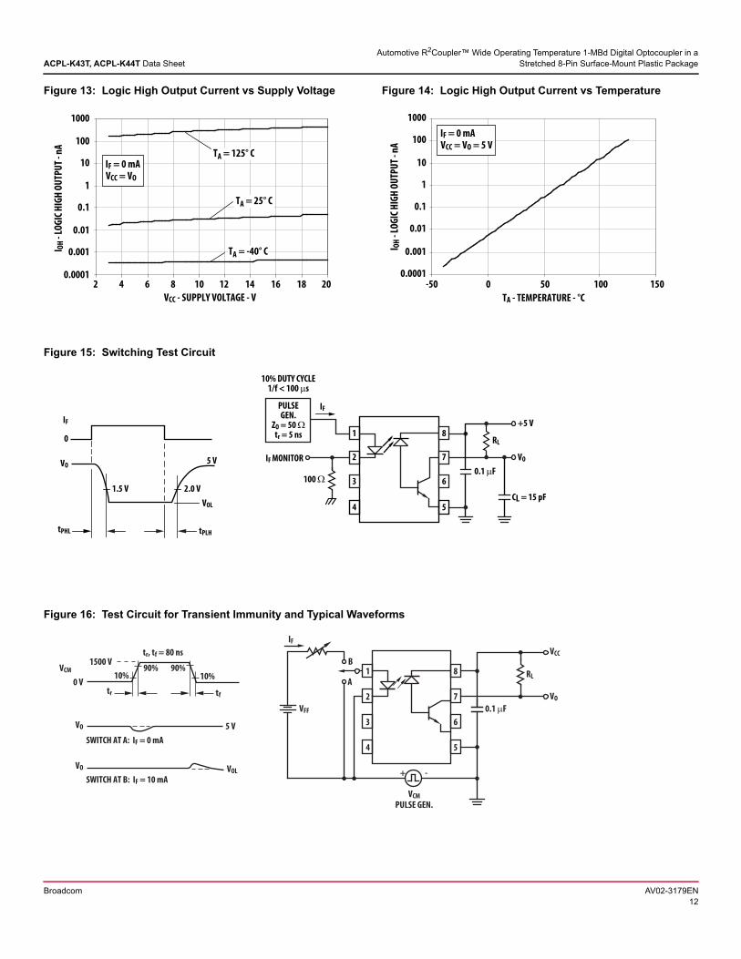
Figure 13: Logic High Output Current vs Supply Voltage Figure 14: Logic High Output Current vs Temperature
I OH
- LO
GIC
HIG
H O
UTP
UT
- nA
0.0001
0.001
0.01
0.1
1
10
100
1000
2 4 6 8 10 12 14 16 18 20
TA = -40° C
TA = 25° C
TA = 125° C
VCC - SUPPLY VOLTAGE - V
IF = 0 mAVCC = VO
TA - TEMPERATURE - °C
I OH
- LO
GIC
HIG
H O
UTP
UT
- nA
0.0001
0.001
0.01
0.1
1
10
100
1000
-50 0 50 100 150
IF = 0 mAVCC = VO = 5 V
Figure 15: Switching Test Circuit
VO
PULSEGEN.
ZO = 50 tr = 5 ns
IF MONITOR
IF
0.1 F
RL
CL = 15 pF
100
0
tPHL tPLH
VO
IF
VOL
1.5 V 2.0 V
5 V
+5 V1
2
4
10% DUTY CYCLE1/f < 100 s
3
8
7
5
6
Figure 16: Test Circuit for Transient Immunity and Typical Waveforms
VO
IF
0.1 F
RLA
B
PULSE GEN.VCM
+
VFF
VO
VOLVO
0 V10%
90% 90%10%
SWITCH AT A: IF = 0 mA
SWITCH AT B: IF = 10 mA
VCM
tr tf
5 V
VCC
-
1500 Vtr, tf = 80 ns
1
2
3
4
8
7
6
5
Broadcom AV02-3179EN12
ACPL-K43T, ACPL-K44T Data Sheet Automotive R2Coupler™ Wide Operating Temperature 1-MBd Digital Optocoupler in a
Stretched 8-Pin Surface-Mount Plastic Package
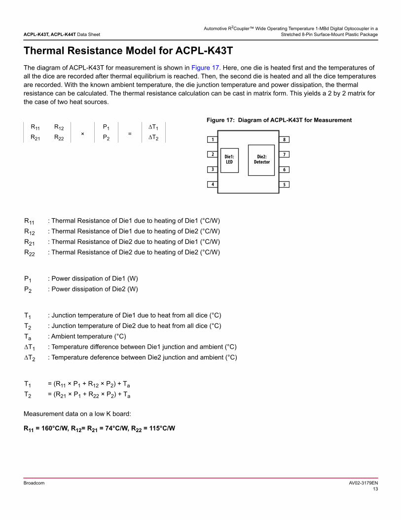
Thermal Resistance Model for ACPL-K43T
The diagram of ACPL-K43T for measurement is shown in Figure 17. Here, one die is heated first and the temperatures of all the dice are recorded after thermal equilibrium is reached. Then, the second die is heated and all the dice temperatures are recorded. With the known ambient temperature, the die junction temperature and power dissipation, the thermal resistance can be calculated. The thermal resistance calculation can be cast in matrix form. This yields a 2 by 2 matrix for the case of two heat sources.
Figure 17: Diagram of ACPL-K43T for MeasurementR11 R12
×P1
=T1
R21 R22 P2 T2 1
2
3
4
8
7
6
5
Die1:LED
Die2:Detector
Measurement data on a low K board:
R11 = 160°C/W, R12= R21 = 74°C/W, R22 = 115°C/W
R11 : Thermal Resistance of Die1 due to heating of Die1 (°C/W)
R12 : Thermal Resistance of Die1 due to heating of Die2 (°C/W)
R21 : Thermal Resistance of Die2 due to heating of Die1 (°C/W)
R22 : Thermal Resistance of Die2 due to heating of Die2 (°C/W)
P1 : Power dissipation of Die1 (W)
P2 : Power dissipation of Die2 (W)
T1 : Junction temperature of Die1 due to heat from all dice (°C)
T2 : Junction temperature of Die2 due to heat from all dice (°C)
Ta : Ambient temperature (°C)
T1 : Temperature difference between Die1 junction and ambient (°C)
T2 : Temperature deference between Die2 junction and ambient (°C)
T1 = (R11 × P1 + R12 × P2) + Ta
T2 = (R21 × P1 + R22 × P2) + Ta
Broadcom AV02-3179EN13
ACPL-K43T, ACPL-K44T Data Sheet Automotive R2Coupler™ Wide Operating Temperature 1-MBd Digital Optocoupler in a
Stretched 8-Pin Surface-Mount Plastic Package
Thermal Resistance Model for ACPL-K44T
The diagram of ACPL-K44T for measurement is shown in Figure 18. Here, one die is heated first and the temperatures of all the dice are recorded after thermal equilibrium is reached. Then, the second, third, and fourth die are heated and all the dice temperatures are recorded. With the known ambient temperature, the die junction temperature and power dissipation, the thermal resistance can be calculated. The thermal resistance calculation can be cast in matrix form. This yields a 4 by 4 matrix for the case of two heat sources.
Figure 18: Diagram of ACPL-K44T for MeasurementR11 R12 R13 R14
×
P1
=
T1
R21 R22 R23 R24 P2 T2
R31 R32 R33 R34 P3 T3
R41 R42 R43 R44 P4 T4
1
2
3
4
8
7
6
5
Die1:LED 1
Die2:Detector 1
Die3:LED 1
Die4:Detector 2
R11 : Thermal Resistance of Die1 due to heating of Die1 (°C/W)
R12 : Thermal Resistance of Die1 due to heating of Die2 (°C/W)
R13 : Thermal Resistance of Die1 due to heating of Die3 (°C/W)
R14 : Thermal Resistance of Die1 due to heating of Die4 (°C/W)
R21 : Thermal Resistance of Die2 due to heating of Die1 (°C/W)
R22 : Thermal Resistance of Die2 due to heating of Die2 (°C/W)
R23 : Thermal Resistance of Die2 due to heating of Die3 (°C/W)
R24 : Thermal Resistance of Die2 due to heating of Die4 (°C/W)
R31 : Thermal Resistance of Die3 due to heating of Die1 (°C/W)
R32 : Thermal Resistance of Die3 due to heating of Die2 (°C/W)
R33 : Thermal Resistance of Die3 due to heating of Die3 (°C/W)
R34 : Thermal Resistance of Die3 due to heating of Die4 (°C/W)
R41 : Thermal Resistance of Die4 due to heating of Die1 (°C/W)
R42 : Thermal Resistance of Die4 due to heating of Die2 (°C/W)
R43 : Thermal Resistance of Die4 due to heating of Die3 (°C/W)
R44 : Thermal Resistance of Die4 due to heating of Die4 (°C/W)
P1 : Power dissipation of Die1 (W)
P2 : Power dissipation of Die2 (W)
P3 : Power dissipation of Die3 (W)
P4 : Power dissipation of Die4 (W)
Broadcom AV02-3179EN14
ACPL-K43T, ACPL-K44T Data Sheet Automotive R2Coupler™ Wide Operating Temperature 1-MBd Digital Optocoupler in a
Stretched 8-Pin Surface-Mount Plastic Package
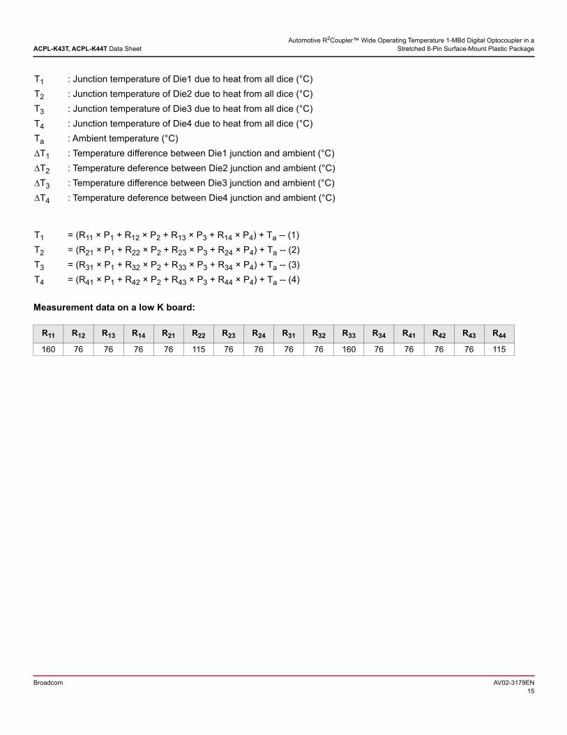
Measurement data on a low K board:
T1 : Junction temperature of Die1 due to heat from all dice (°C)
T2 : Junction temperature of Die2 due to heat from all dice (°C)
T3 : Junction temperature of Die3 due to heat from all dice (°C)
T4 : Junction temperature of Die4 due to heat from all dice (°C)
Ta : Ambient temperature (°C)
T1 : Temperature difference between Die1 junction and ambient (°C)
T2 : Temperature deference between Die2 junction and ambient (°C)
T3 : Temperature difference between Die3 junction and ambient (°C)
T4 : Temperature deference between Die4 junction and ambient (°C)
T1 = (R11 × P1 + R12 × P2 + R13 × P3 + R14 × P4) + Ta -- (1)
T2 = (R21 × P1 + R22 × P2 + R23 × P3 + R24 × P4) + Ta -- (2)
T3 = (R31 × P1 + R32 × P2 + R33 × P3 + R34 × P4) + Ta -- (3)
T4 = (R41 × P1 + R42 × P2 + R43 × P3 + R44 × P4) + Ta -- (4)
R11 R12 R13 R14 R21 R22 R23 R24 R31 R32 R33 R34 R41 R42 R43 R44
160 76 76 76 76 115 76 76 76 76 160 76 76 76 76 115
Broadcom AV02-3179EN15

Broadcom, the pulse logo, Connecting everything, Avago Technologies, Avago, the A logo, and R2Coupler are among the trademarks of Broadcom and/or its affiliates in the United States, certain other countries, and/or the EU.
Copyright © 2012–2018 Broadcom. All Rights Reserved.
The term “Broadcom” refers to Broadcom Inc. and/or its subsidiaries. For more information, please visit www.broadcom.com.
Broadcom reserves the right to make changes without further notice to any products or data herein to improve reliability, function, or design. Information furnished by Broadcom is believed to be accurate and reliable. However, Broadcom does not assume any liability arising out of the application or use of this information, nor the application or use of any product or circuit described herein, neither does it convey any license under its patent rights nor the rights of others.