acpl-m50l, acpl-054l, acpl-w50l, acpl-k54l - · pdf filelow power, 1 mbd digital optocoupler...
TRANSCRIPT
ACPL-M50L, ACPL-054L, ACPL-W50L, ACPL-K54LLow Power, 1 MBd Digital Optocoupler
Data Sheet
DescriptionThe Broadcom® ACPL-M50L (single-channel in SO-5 footprint), ACPL-054L (dual-channel in SO-8 footprint), ACPL-W50L (single-channel in stretched SO-6 footprint), and ACPL-K54L (dual-channel in stretched SO-8 footprint) are low power, low-input current, 1-MBd digital optocouplers.
These digital optocouplers use an insulating layer between the light-emitting diode and an integrated photon detector to provide electrical insulation between input and output. Separate connections for the photodiode bias and output transistor collector increase the speed up to a hundred times over that of a conventional photo-transistor coupler by reducing the base-collector capacitance.
The ACPL-M50L/054L/W50L/K54L has an increased common mode transient immunity of 15 kV/μs minimum at VCM = 1500V over a temperature range of –40°C to 105°C. The current transfer ratio (CTR) is 140% typical for ACPL-M50L or 130% typical for ACPL-054L/W50L/K54L at IF = 3mA. This digital optocoupler can be used in any TTL/CMOS, TTL/LSTTL, or wide bandwidth analog applications.
CAUTION Take normal static precautions in handling and assembly of this component to prevent damage and/or degradation that might be induced by electrostatic discharge (ESD). The components featured in this data sheet are not to be used in military or aerospace applications or environments
Features Wide supply voltage Vcc: 2.7V to 24V Low drive current: 3 mA Open-collector output TTL compatible Compact SO-5, SO-8, stretched SO-6, and stretched SO-8
package 15 kV/μs high common-mode rejection at VCM = 1500V Guaranteed performance from temperature range: –40°C
to +105°C Low propagation delay: 1 μs max at 5V Worldwide safety approval:
— UL1577 recognized, 3750 Vrms/1 min for ACPL-M50L/054L, 5000 Vrms/1 min for ACPL-W50L/K54L
— CSA Approval— IEC/EN/DIN EN 60747-5-5 Approval for Reinforced
Insulation
Applications Communications interface Digital signal isolation Micro-controller interface Feedback elements in switching power supplies Digital isolation for A/D, D/A conversion digital field
Broadcom- 1 -

ACPL-M50L, ACPL-054L, ACPL-W50L, ACPL-K54L Data Sheet
Figure 1 Functional Diagram
NOTE The connection of a 0.1-μF bypass capacitor between pins 4 and 6 for ACPL-M50L/W50L and between pins 5 and 8 for ACPL-054L/K54L is recommended.
Table 1 Truth Table
LED VO
ON LOW
OFF HIGH
7
1
2
3
4 5
6
8
ACPL-054L/K54L
5
1
34
6
ACPL-M50L ACPL-W50L
1
2
3
6
5
4
VO
Anode
CathodeGND
VCC
VO
GND
VCC
NC
Cathode
Anode
VO1
GND
VO2
VCC
Cathode1
Anode2
Cathode2
Anode1
Broadcom- 2 -

ACPL-M50L, ACPL-054L, ACPL-W50L, ACPL-K54L Data Sheet
Ordering InformationACPL-M50L and ACPL-054L are UL Recognized with 3750 Vrms for 1 minute per UL1577. ACPL-W50L and ACPL-K54L are UL Recognized with 5000 Vrms for 1 minute per UL1577.
To order, choose a part number from the part number column and combine with the desired option from the option column to form an order entry.
Example 1:
ACPL-M50L-500E to order product of Mini-flat Surface Mount 5-pin package in Tape and Reel packaging with RoHS compliant.
Option data sheets are available. Contact your Broadcom sales representative or authorized distributor for information.
Table 2 Ordering Information
Part Number
Option
Package Surface Mount Tape and Reel IEC/EN 60747-5-5 QuantityRoHS
Compliant
ACPL-M50L -000E SO-5 X 100 per tube
-060E X X 100 per tube
-500E X X 1500 per reel
-560E X X X 1500 per reel
ACPL-054L -000E SO-8 X 100 per tube
-060E X X 100 per tube
-500E X X 1500 per reel
-560E X X X 1500 per reel
ACPL-W50L -000E Stretched SO-6 X 100 per tube
-060E X X 100 per tube
-500E X X 1000 per reel
-560E X X X 1000 per reel
ACPL-K54L -000E Stretched SO-8 X 80 per tube
-060E X X 80 per tube
-500E X X 1000 per reel
-560E X X X 1000 per reel
Broadcom- 3 -

ACPL-M50L, ACPL-054L, ACPL-W50L, ACPL-K54L Data Sheet
Package Outline Drawings
Figure 2 ACPL-M50L SO-5 Package (JEDEC M0-155)
Figure 3 Land Pattern Recommendations
M50LYWW 7.0 ± 0.2
(0.276 ± 0.008)
2.5 ± 0.1(0.098 ± 0.004)
0.102 ± 0.102(0.004 ± 0.004)
4.4 ± 0.1(0.173 ± 0.004)
1.27(0.050) BSC
0.216 ± 0.038(0.0085 ± 0.0015)
0.71(0.028) MIN
0.4 ± 0.05(0.016 ± 0.002)
3.6 ± 0.1*(0.142 ± 0.004)
Dimensions in Millimeters (Inches)* Maximum mold flash on each side is 0.15 mm (0.006)Note: Floating lead protrusion is 0.15 mm (6 mils) max.
7° MAX.
MAX. LEAD COPLANARITY= 0.102 (0.004)
EEE
6
5
43
1 VCC
VOUT
GNDCATHODE
ANODE
LOT ID
DATE CODE
PART NUMBER
8.27(0.325)
1.8(0.072)
2.5(0.10)
1.3(0.05)
0.64(0.025)
4.4(0.17)
Dimension in Millimeters (Inches)
Broadcom- 4 -

ACPL-M50L, ACPL-054L, ACPL-W50L, ACPL-K54L Data Sheet
Figure 4 ACPL-054L (Small Outline SO-8 Package)
54LVYWW
8 7 6 5
4321
5.994 ± 0.203(0.236 ± 0.008)
3.937 ± 0.127(0.155 ± 0.005)
0.406 ± 0.076(0.016 ± 0.003) 1.270
(0.050)BSC
5.080 ± 0.127(0.200 ± 0.005)
3.175 ± 0.127(0.125 ± 0.005) 1.524
(0.060)
45° X0.432
(0.017)
0.228 ± 0.025(0.009 ± 0.001)
TYPE NUMBER(‘V’ for OPTION 060)
DATE CODE
LEAD FREE
0.305(0.012)
MIN.
0.203 ± 0.102(0.008 ± 0.004)
7°
PIN ONE
0 ~ 7°
*
Total package length (inclusive of mold flash)5.207 ± 0.254 (0.205 ± 0.010)Dimensions in Millimeters (Inches).Lead coplanarity = 0.10 mm (0.004 inches) max.Option number 500 not marked.Note: Floating lead protrusion is 0.15 mm (6 mils) max.
*
7.49 (0.295)
1.9 (0.075)
0.64 (0.025)
LAND PATTERN RECOMMENDATION
XXX
LOT ID
Broadcom- 5 -

ACPL-M50L, ACPL-054L, ACPL-W50L, ACPL-K54L Data Sheet
Figure 5 ACPL-W50L Stretched SO-6 Package
*4.480±0.254(0.180±0.010)
45°
0.381±0.127(0.015±0.005)
1.27 (0.050) BSG
0.20±0.10(0.008±0.004)
0.45 (0.018)
0.750±0.250 (0.0295±0.010) 11.50±0.250
(0.453±0.010)
6.807
0.268
* Total package width (inclusive of mold flash) 4.834 ± 0.254 mm
7°
12.65 (0.498)
LAND PATTERN RECOMMENDATION
3.180±0.127 (0.125±0.005)
1.590±0.127(0.063±0.005)
7°
1.91 (0.075)
321
456
0.76 (0.030)
+0.127 0+0.005 - 0.000
)(
W50LYWW
PART NUMBER
DATE CODE
ROHS-COMPLIANCEINDICATOR
Dimensions in Millimeters (Inches).Lead coplanarity = 0.1 mm (0.004 inches).
EEE
LOT ID
Broadcom- 6 -

ACPL-M50L, ACPL-054L, ACPL-W50L, ACPL-K54L Data Sheet
Figure 6 ACPL-K54L Stretched SO-8 Package
Solder Reflow ProfileRecommended reflow condition as per JEDEC Standard, J-STD-020 (latest revision). Non-halide flux should be used.
Regulatory InformationThe ACPL-M50L/054L/W50L/K54L is approved by the following organizations.
UL Approval under UL 1577, component recognition program up to VISO = 3750 VRMS for ACPL-M50L/054L and VISO = 5000 VRMS for ACPL-W50L/K54L.
CSA Approval under CSA Component Acceptance Notice #5.
IEC/EN 60747-5-5 (Option 060E only).
40.381±0.13 (0.015±0.005)
1.270 (0.050) BSG
12.650 (0.5)
1.905 (0.1)
321
5678
*5.850±0.254(0.230±0.010)
LAND PATTERN RECOMMENDATION
* Total package width (inclusive of mold flash) 6.100 ± 0.250 mmDimensions in Millimeters (Inches).Lead coplanarity = 0.1 mm (0.004 inches).
7° 45°
0.200±0.100(0.008±0.004)
0.450 (0.018)
0.750±0.250 (0.0295±0.010) 11.5±0.250
(0.453±0.010)
6.807±0.127(0.268±0.005)
7°
3.180±0.127 (0.125±0.005)
1.590±0.127 (0.063±0.005)
K54LYWW
PART NUMBER
DATE CODE
ROHS-COMPLIANCEINDICATOR
EEE
LOT ID
Broadcom- 7 -

ACPL-M50L, ACPL-054L, ACPL-W50L, ACPL-K54L Data Sheet
NOTE These optocouplers are suitable for "safe electrical isolation" only within the safety limit data. Maintenance of the safety limit data shall be ensured by means of protective circuits.
Table 3 Insulation and Safety Related Specifications
Parameter Symbol ACPL-M50L ACPL-054L ACPL-W50L ACPL-K54L Units Conditions
Minimum External Air Gap (Clearance)
L(101) 5 4.9 8 mm Measured from input terminals to output terminals, shortest distance through air.
Minimum External Tracking (Creepage)
L(102) 5 4.8 8 mm Measured from input terminals to output terminals, shortest distance path along body.
Minimum Internal Plastic Gap (Internal Clearance)
0.08 0.08 0.08 mm Through insulation distance conductor to conductor, usually the straight line distance thickness between the emitter and detector.
Tracking Resistance (Comparative Tracking Index)
CTI 175 175 175 V DIN IEC 112/VDE 0303 Part 1
Isolation Group IIIa IIIa IIIa — Material Group (DIN VDE 0110, 1/89, Table 1)
Table 4 IEC/EN60747-5-5 Insulation Characteristicsa (Option 060E)
a. Refer to the optocoupler section of the Isolation and Control Components Designer’s Catalog, under Product Safety Regulations section, (IEC/EN 60747-5-5) for a detailed description of Method a and Method b partial discharge test profiles.
Description Symbol
Characteristic
UnitsACPL-M50L/ 054L
ACPL-W50L/ K54L
Installation classification per DIN VDE 0110/39, Table 1for rated mains voltage ≤ 150 Vrms
for rated mains voltage ≤ 300 Vrms
for rated mains voltage ≤ 600 Vrms
for rated mains voltage ≤ 1000 Vrms
I – IV
I – III
I – II
I – IV
I – IV
I – III
I – III
—
Climatic Classification 55/105/21 55/105/21 —
Pollution Degree (DIN VDE 0110/39) 2 2 —
Maximum Working Insulation Voltage VIORM 560 1140 Vpeak
Input to Output Test Voltage, Method ba VIORM × 1.875 = VPR, 100% Production Test with tm = 1s, Partial discharge < 5 pC
VPR 1050 2137 Vpeak
Input to Output Test Voltage, Method aa VIORM × 1.6 = VPR, Type and Sample Test, tm = 10s, Partial discharge < 5 pC
VPR 896 1824 Vpeak
Highest Allowable Overvoltage (Transient Overvoltage tini = 60s) VIOTM 6000 8000 Vpeak
Safety-limiting values – maximum values allowed in the event of a failure.
Case Temperature
Input Currentb
Output Powerb
b. Refer to the following figure for dependence of PS and IS on ambient temperature.
TS
IS, INPUT
PS, OUTPUT
150
150
600
175
230
600
°C
mA
mW
Insulation Resistance at TS, VIO = 500 V RS >109 >109
Broadcom- 8 -

ACPL-M50L, ACPL-054L, ACPL-W50L, ACPL-K54L Data Sheet
Table 5 Absolute Maximum Ratings
Parameter Symbol Min. Max. Units
Storage Temperature TS –55 125 °C
Operating Temperature TA –40 105 °C
Lead Soldering Cycle Temperature — 260 °C
Time — 10 s
Average Forward Input Currenta
a. Derate linearly above 85°C free-air temperature at a rate of 0.5 mA/°C.
IF(avg) — 20 mA
Peak Forward Input Currentb (50% duty cycle, 1-ms pulse width)
b. Derate linearly above 85°C free-air temperature at a rate of 1.0 mA/°C.
IF(peak) — 40 mA
Peak Transient Input Current (≤1 μs pulse width, 300 ps) IF(trans) — 1 A
Reversed Input Voltage VR — 5 V
Input Power Dissipationc
c. Derate linearly above 85°C free-air temperature at a rate of 0.9 mW/°C.
PIN — 36 mW
Output Power Dissipationd
d. Derate linearly above 85°C free-air temperature at a rate of 1.2 mW/°C.
PO — 45 mW
Average Output Current IO(AVG) — 8 mA
Peak Output Current IO(PEAK) — 16 mA
Supply Voltage VCC –0.5 30 V
Output Voltage VO –0.5 24 V
Solder Reflow Temperature Profile See Package Outline Drawings
Table 6 Recommended Operating Conditions
Parameter Symbol Min. Max. Units
Supply Voltage VCC 2.7 24 V
Input Current, High Level IFH 3 10 mA
Operating Temperature TA –40 105 °C
Forward Input Voltage (OFF) VF (OFF) — 0.8 V
Broadcom- 9 -

ACPL-M50L, ACPL-054L, ACPL-W50L, ACPL-K54L Data Sheet
Electrical Specifications (DC)Over recommended temperature (TA = –40°C to +105°C) and supply voltage (2.7V ≤ VCC ≤ 24V). All typical specifications are at TA = 25°C.
Table 7 Electrical Specifications (DC)
Parameter Sym. Part Number Min. Typ. Max. Units Conditions Figure
Current Transfer Ratio
CTRa
a. CURRENT TRANSFER RATIO in percent is defined as the ratio of output collector current, IO, to the forward LED input current, IF, times 100%.
ACPL-M50L 100 140 200 % TA = 25°C VO = 0.4V VCC = 3.3V or 5V, IF = 3 mA
8, 9
80 — — % VO = 0.5V
ACPL-054L ACPL-W50L ACPL-K54L
93 130 200 % TA = 25°C VO = 0.4V VCC= 3.3V or 5V, IF = 3 mA
8, 9
53 — — % VO = 0.5V
Logic Low Output Voltage
VOL — 0.2 0.4 V TA = 25°C IO = 3 mA VCC = 3.3V or 5V, IF = 3 mA— 0.2 0.5 V IO = 1.6 mA
Logic High Output Current
IOH — 0.003 0.5 μA TA = 25°C VO = VCC = 5.5V IF =0 mA 10, 11
— 0.01 1 VO = VCC = 24V
— — 80 VO = VCC = 24V
Logic Low Supply Currentper Channel
ICCL — 36 100 μA IF = 3 mA, VO = open, VCC = 24V
Logic High Supply Current per Channel
ICCH — 0.02 2 μA IF = 0 mA, VO = open, VCC = 24V
Input Forward Voltage
VF — 1.5 1.8 V TA= 25°C IF = 3 mA 7
— 1.5 1.95 V IF = 3 mA
Input Reversed Breakdown Voltage
BVR 5 — — V IR = 10 μA
Temperature Coefficient of Forward Voltage
VF/TA — –1.6 — mV/°C IF= 3 mA
Input Capacitance CIN — 77 — pF F = 1 MHz, VF = 0
Broadcom- 10 -

ACPL-M50L, ACPL-054L, ACPL-W50L, ACPL-K54L Data Sheet
Switching Specifications (ACPL-M50L) Over recommended operating (TA = –40°C to 105°C), IF = 3 mA, (2.7V ≤ VCC ≤ 24V), unless otherwise specified.
Table 8 Switching Specifications (ACPL-M50L)
Parameter Symbol Min Typ Max Units Test Conditions Figure
Propagation Delay Time to Logic Low at Output
TPHL — 0.2 0.5 μs TA = 25°C Pulse: f = 10 kHz, Duty cycle = 50%, IF = 3 mA, VCC = 3.3V, RL= 1.2 k, CL = 15 pF, VTHHL = 1.5V
26
— 0.2 1 μs 12, 26
— 0.22 0.5 μs TA = 25°C Pulse: f = 10 kHz, Duty cycle = 50%, IF = 3 mA, VCC = 5.0V, RL = 1.9 k, CL = 15 pF, VTHHL = 1.5V
26
— 0.22 1 μs 14, 26
— 0.33 0.7 μs TA = 25°C Pulse: f = 10 kHz, Duty cycle = 50%, IF = 3 mA, VCC = 24V, RL = 10 k, CL = 15 pF, VTHHL = 1.5V
26
— 0.33 1.3 μs 16, 26
Propagation Delay Time to Logic High at Output
TPLH — 0.38 0.8 μs TA = 25°C Pulse: f = 10 kHz, Duty cycle = 50%, IF = 3 mA, VCC = 3.3V, RL = 1.2 k, CL = 15 pF, VTHHL = 2.0V
26
— 0.38 1.2 μs 12, 26
— 0.31 0.7 μs TA = 25°C Pulse: f = 10 kHz, Duty cycle = 50%, IF= 3 mA, VCC = 5.0V, RL = 1.9 k, CL = 15 pF, VTHHL = 2.0V
26
— 0.31 1 μs 14, 26
— 0.3 0.7 μs TA = 25°C Pulse: f = 10 kHz, Duty cycle = 50%, IF = 3 mA, VCC = 24V, RL = 10 k, CL = 15 pF, VTHHL = 2.0V
26
— 0.3 1 μs 16, 26
Pulse Width Distortiona
a. Pulse Width Distortion (PWD) is defined as |tPHL – tPLH| for any given device.
PWD — 0.18 0.8 μs TA = 25°C Pulse: f = 10 kHz, Duty cycle = 50%, IF = 3 mA, VCC = 3.3V, RL = 1.2 k, CL = 15 pF, VTHHL = 1.5V, VTHLH = 2.0V
26
— 0.18 1.2 μs 26
— 0.1 0.7 μs TA = 25°C Pulse: f = 10 kHz, Duty cycle = 50%, IF = 3 mA, VCC = 5.0V, RL = 1.9 k, CL = 15 pF, VTHHL = 1.5V, VTHLH = 2.0V
26
— 0.1 1 μs 26
— 0.1 0.7 μs TA = 25°C Pulse: f = 10 kHz, Duty cycle = 50%, IF = 3 mA, VCC=24V, RL=10 k, CL=15 pF, VTHHL=1.5V, VTHLH=2.0V
26
— 0.1 1 μs 26
Propagation Delay Difference Between Any Two Partsb
b. The difference between tPLH and tPHL between any two parts under the same test condition. (See IPM Dead Time and Propagation Delay Specifications section.)
tpsk — 0.18 0.7 μs TA = 25°C Pulse: f = 10 kHz, Duty cycle = 50%, IF = 3 mA, VCC = 3.3V, RL = 1.2 k, CL = 15 pF, VTHHL = 1.5V, VTHLH = 2.0V
— 0.1 0.6 μs TA = 25°C Pulse: f = 10 kHz, Duty cycle = 50%, IF = 3 mA, VCC = 5.0V, RL = 1.9 k, CL = 15 pF, VTHHL = 1.5V, VTHLH = 2.0V
— 0.1 0.6 μs TA = 25°C Pulse: f = 10 kHz, Duty cycle = 50%, IF = 3 mA, VCC = 24V, RL = 10 k, CL = 15 pF, VTHHL = 2.0V
Common Mode Transient Immunity at Logic High Outputc
c. Common transient immunity in a Logic High level is the maximum tolerable (positive) dVCM/dt on the rising edge of the common mode pulse, VCM, to assure that the output will remain in a Logic High state (that is, VO > 2.0V).
|CMH| 15 25 — kV/μs TA = 25°C VCM = 1500V, IF = 0 mA,, RL = 1.2 k or 1.9 k, VCC = 3.3V or 5V
27
Common Mode Transient Immunity at Logic Low Outputd
d. Common mode transient immunity in a Logic Low level is the maximum tolerable (negative) dVCM/dt on the falling edge of the common mode pulse signal, VCM to assure that the output will remain in a Logic Low state (that is, VO < 0.8V).
|CML| 15 20 — kV/μs TA= 25°C VCM = 1500V, IF = 3 mA, RL = 1.2 k, VCC = 5V 27
10 15 — kV/μs VCM = 1500V, IF = 3 mA, RL = 1.2 k, VCC = 3.3V 27
Broadcom- 11 -
ACPL-M50L, ACPL-054L, ACPL-W50L, ACPL-K54L Data Sheet
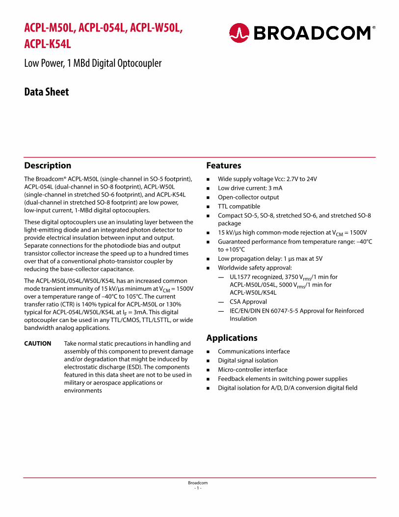
Switching Specifications (ACPL-054L/W50L/K54L)Over recommended temperature (TA = –40°C to +105°C), supply voltage (2.7V ≤ VCC ≤ 24V) unless otherwise specified.
Table 9 Switching Specifications (ACPL-054L/W50L/K54L)
Parameter Symbol Min Typ Max Units Test Conditions Figure
Propagation Delay Time to Logic Low at Output
TPHL — 0.2 0.5 μs TA = 25°C Pulse: f = 10 kHz, Duty cycle = 50%, IF = 3 mA, VCC = 3.3V, RL = 1.8 k, CL = 15 pF, VTHHL = 1.5V
26
— 0.2 1 μs 13, 26
— 0.22 0.5 μs TA = 25°C Pulse: f = 10 kHz, Duty cycle = 50%, IF = 3 mA, VCC = 5.0V, RL = 2.9 k, CL = 15 pF, VTHHL = 1.5V
26
— 0.22 1 μs 15, 26
— 0.33 0.7 μs TA = 25°C Pulse: f = 10 kHz, Duty cycle = 50%, IF = 3 mA, VCC = 24V, RL = 14.8 k, CL = 15 pF, VTHHL= 1.5V
26
— 0.33 1.3 μs 17, 26
Propagation Delay Time to Logic High at Output
TPLH — 0.38 0.8 μs TA = 25°C Pulse: f = 10 kHz, Duty cycle = 50%, IF = 3 mA, VCC = 3.3V, RL = 1.8 k, CL =1 5 pF, VTHHL = 2.0V
26
— 0.38 1.4 μs 13, 26
— 0.31 0.7 μs TA = 25°C Pulse: f = 10 kHz, Duty cycle = 50%, IF = 3 mA, VCC = 5.0V, RL = 2.9 k, CL = 15 pF, VTHHL = 2.0V
26
— 0.31 1 μs 15, 26
— 0.3 0.7 μs TA = 25°C Pulse: f = 10 kHz, Duty cycle = 50%, IF = 3 mA, VCC = 24V, RL = 14.8 k, CL = 15 pF, VTHHL = 2.0V
26
— 0.3 1 μs 17, 26
Pulse Width Distortiona
a. Pulse Width Distortion (PWD) is defined as |tPHL – tPLH| for any given device.
PWD — 0.18 0.8 μs TA = 25°C Pulse: f = 10 kHz, Duty cycle = 50%, IF = 3 mA, VCC = 3.3V, RL = 1.8 k, CL = 15 pF, VTHH L= 1.5V, VTHLH = 2.0V
26
— 0.18 1.4 μs 26
— 0.1 0.7 μs TA = 25°C Pulse: f = 10 kHz, Duty cycle = 50%, IF= 3 mA, VCC =5.0V, RL = 2.9 k, CL = 15 pF, VTHHL = 1.5V, VTHLH = 2.0V
26
— 0.1 1 μs 26
— 0.1 0.7 μs TA = 25°C Pulse: f = 10 kHz, Duty cycle = 50%, IF = 3 mA, VCC = 24V, RL = 14.8 k, CL = 15 pF, VTHHL = 1.5V, VTHLH = 2.0V
26
— 0.1 1 μs 26
Propagation Delay Difference Between Any Two Partsb
b. The difference between tPLH and tPHL between any two parts under the same test condition. (See IPM Dead Time and Propagation Delay Specifications section.)
tpsk — 0.18 0.7 μs TA = 25°C Pulse: f = 10 kHz, Duty cycle = 50%, IF= 3 mA, VCC = 3.3V, RL = 1.8 k, CL = 15 pF, VTHHL = 1.5V, VTHLH = 2.0V
— 0.1 0.6 μs TA = 25°C Pulse: f = 10 kHz, Duty cycle = 50%, IF = 3 mA, VCC = 5.0V, RL = 2.9 k, CL = 15 pF, VTHHL = 1.5V, VTHLH = 2.0V
— 0.1 0.6 μs TA = 25°C Pulse: f = 10 kHz, Duty cycle = 50%, IF = 3 mA, VCC = 24V, RL = 14.8 k, CL = 15 pF, VTHHL = 2.0V, VTHLH = 2.0V
Common Mode Transient Immunity at Logic High Outputc
c. Common transient immunity in a Logic High level is the maximum tolerable (positive) dVCM/dt on the rising edge of the common mode pulse, VCM, to assure that the output will remain in a Logic High state (this is, VO > 2.0V).
|CMH| 15 25 — kV/μs TA = 25°C VCM = 1500V, IF = 0 mA,, RL = 1.8 k or 2.9 k, VCC = 3.3V or 5V
27
Common Mode Transient Immunity at Logic Low Outputd
d. Common mode transient immunity in a Logic Low level is the maximum tolerable (negative) dVCM/dt on the falling edge of the common mode pulse signal, VCM to assure that the output will remain in a Logic Low state (that is, VO < 0.8V).
|CML| 15 20 — kV/μs TA= 25°C VCM = 1500V, IF = 3 mA, RL = 2.9 k, VCC = 5V 27
15 20 — kV/μs VCM = 1500V, IF = 3 mA, RL = 1.8 k, VCC = 3.3V 27
Broadcom- 12 -

ACPL-M50L, ACPL-054L, ACPL-W50L, ACPL-K54L Data Sheet
Package CharacteristicsAll typical at TA = 25°C.
Table 10 Package Characteristics
Parameter Symbol Part Number Min. Typ. Max. Units Test Conditions
Input-Output Momentary Withstand Voltagea,b
a. Device considered a two terminal device: pins 1 and 3 shorted together and pins 4, 5, and 6 shorted together for ACPL-M50L, pins 1, 2, 3, and 4 shorted together and pins 5, 6, 7, and 8 shorted together for ACPL-054L/K54L, pins 1, 2, and 3 shorted together and pins 4, 5, and 6 shorted together for ACPL-W50L.
b. In accordance with UL 1577, each optocoupler is proof tested by applying an insulation test voltage ≥ 4500 VRMS for 1 second for ACPL-M50L/054L and ≥ 6000 VRMS for 1 second for ACPL-W50L/K54L (leakage detection current limit, II-O ≤ 5mA).
VISO ACPL-M50L/054L 3750 — — Vrms RH ≤ 50%, t = 1 min., TA = 25°C
ACPL-W50L/K54L 5000 — —
Input-Output Resistancea RI-O — 1014 — VI-O = 500 Vdc
Input-Output Capacitancea CI-O — 0.6 — pF f = 1 MHz, TA = 25°C
Input-Input Insulation Leakage Current[3]
II-I — 0.005 — μA RH ≤ 45%, t = 5s, VI-I = 500 Vdc
Input-Input Resistancec
c. Measured between pins 1 and 2 shorted together and pins 3 and 4 shorted together for ACPL-054L/K54L.
RI-I — 1011 —
Input-Input Capacitancec CI-I — 0.25 — pF f = 1 MHz
Broadcom- 13 -
ACPL-M50L, ACPL-054L, ACPL-W50L, ACPL-K54L Data Sheet
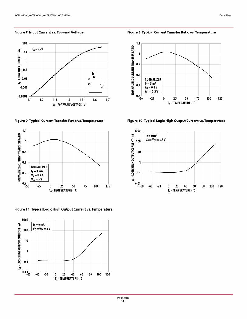
Figure 7 Input Current vs. Forward Voltage Figure 8 Typical Current Transfer Ratio vs. Temperature
VF - FORWARD VOLTAGE - V
I F - F
ORW
ARD
CURR
ENT -
mA
0.0001
0.001
0.01
0.1
1
10
100
1.1 1.2 1.3 1.4 1.5 1.6 1.7
IF
VF
TA = 25°C
0.6
0.7
0.8
0.9
1
1.1
-50 -25 0 25 50 75 100 125TA - TEMPERATURE - °C
NORM
ALIZ
ED CU
RREN
T TRA
NSFE
R RA
TIO
NORMALIZEDIF = 3 mAVO = 0.4 VVCC = 3.3 V
Figure 9 Typical Current Transfer Ratio vs. Temperature Figure 10 Typical Logic High Output Current vs. Temperature
0.6
0.7
0.8
0.9
1
1.1
-50 -25 0 25 50 75 100 125
NORM
ALIZ
ED CU
RREN
T TRA
NSFE
R RA
TIO
NORMALIZEDIF = 3 mAVO = 0.4 VVCC = 5 V
TA - TEMPERATURE - °C
0.01
0.1
1
10
100
1000
-60 -40 -20 0 20 40 60 80 100 120
I OH -
LOGI
C HIG
H OU
TPUT
CURR
ENT -
nA
TA - TEMPERATURE - °C
IF = 0 mAVO = VCC = 3.3 V
Figure 11 Typical Logic High Output Current vs. Temperature
0.01
0.1
1
10
100
1000
-60 -40 -20 0 20 40 60 80 100 120
IF = 0 mAVO = VCC = 5 V
I OH -
LOGI
C HIG
H OU
TPUT
CURR
ENT -
nA
TA - TEMPERATURE - °C
Broadcom- 14 -

ACPL-M50L, ACPL-054L, ACPL-W50L, ACPL-K54L Data Sheet
Figure 12 Typical Propagation Delay vs. Temperature (ACPL-M50L)
Figure 13 Typical Propagation Delay vs. Temperature (ACPL-054L/W50L/K54L)
0
100
200
300
400
500
600
700
800
-60 -40 -20 0 20 40 60 80 100 120
t p - P
ROPA
GATI
ON D
ELAY
- ns
tPLH
tPHL
IF = 3 mA, VCC = 3.3 VRL = 1.9 kRL = 1.2 k
TA - TEMPERATURE - °C
0
100
200
300
400
500
600
700
800
-60 -40 -20 0 20 40 60 80 100 120
t p - P
ROPA
GATI
ON D
ELAY
- ns
IF = 3 mA, VCC = 3.3 VRL = 1.8 k
TA - TEMPERATURE - °C
tPLH
tPHL
Figure 14 Typical Propagation Delay vs. Temperature (ACPL-M50L)
Figure 15 Typical Propagation Delay vs. Temperature (ACPL-054L/W50L/K54L)
t p - P
ROPA
GATI
ON D
ELAY
- ns
TA - TEMPERATURE - °C
0
100
200
300
400
500
600
700
800
-60 -40 -20 0 20 40 60 80 100 120
tPLH
tPHL
IF = 3 mA, VCC = 5 VRL = 4.1 kRL = 1.9 k
TA - TEMPERATURE - °C
t p - P
ROPA
GATI
ON D
ELAY
- ns
0
100
200
300
400
500
600
700
800
-60 -40 -20 0 20 40 60 80 100 120
IF = 3 mA, VCC = 5 VRL = 2.9 k
tPLHtPHL
Figure 16 Typical Propagation Delay vs. Temperature (ACPL-M50L)
Figure 17 Typical Propagation Delay vs. Temperature (ACPL-054L/W50L/K54L)
t p - P
ROPA
GATI
ON D
ELAY
- ns
TA - TEMPERATURE - °C
0
100
200
300
400
500
600
-60 -40 -20 0 20 40 60 80 100 120
tPLH
tPHL
IF = 3 mA, VCC = 24 VRL = 20 kRL = 10 k
TA - TEMPERATURE - °C
t p - P
ROPA
GATI
ON D
ELAY
- ns
0
100
200
300
400
500
600
-60 -40 -20 0 20 40 60 80 100 120
tPLH
tPHL
IF = 3 mA, VCC = 24 VRL = 14.8 k
Broadcom- 15 -

ACPL-M50L, ACPL-054L, ACPL-W50L, ACPL-K54L Data Sheet
Figure 18 Typical Propagation Delay vs. Load Resistance Figure 19 Typical Propagation Delay vs. Load Resistance
t p - P
ROPA
GATI
ON D
ELAY
- ns
0
200
400
600
800
1000
1200
1400
1600
1 10RL - LOAD RESISTANCE - k
tPLH
tPHL
IF = 3 mA, VCC = 3.3 VIF = 10 mAIF = 3 mA
t p - P
ROPA
GATI
ON D
ELAY
- ns
RL - LOAD RESISTANCE - k
0100200
300400500600700
800900
1000
1 10
tPLH tPHL
IF = 3 mA, VCC = 5 VIF = 10 mAIF = 3 mA
Figure 20 Typical Propagation Delay vs. Load Capacitance (ACPL-M50L)
Figure 21 Typical Propagation Delay vs. Load Capacitance (ACPL-054L/W50L/K54L)
t p - P
ROPA
GATI
ON D
ELAY
- ns
0200400600800
100012001400160018002000220024002600
0 100 200 300 400 500CL - LOAD CAPACITANCE - pF
tPLHtPHL
IF = 3 mA, VCC = 24 VRL = 10 k , TA = 25°C
t p - P
ROPA
GATI
ON D
ELAY
- ns
CL - LOAD CAPACITANCE - pF
0200400600800
100012001400160018002000220024002600
0 100 200 300 400 500
tPLH
tPHL
IF = 3 mA, VCC = 24 VRL = 14.8 k , TA = 25°C
Figure 22 Typical Propagation Delay vs. Supply Voltage (ACPL-M50L)
Figure 23 Typical Propagation Delay vs. Supply Voltage (ACPL-054L/W50L/K54L)
tp - P
ROPA
GATI
ON D
ELAY
- ns
0
500
1000
1500
2000
2500
8 10 14 20VCC - SUPPLY VOLTAGE - V
tPLH
tPHL
2412 16 2218
IF = 3 mARL = 10 kTA = 25°C
0
500
1000
1500
2000
2500
8
tPLH
tPHL
tp - P
ROPA
GATI
ON D
ELAY
- ns
VCC - SUPPLY VOLTAGE - V2410 14 2012 16 2218
IF = 3 mARL = 14.8 kTA = 25°C
Broadcom- 16 -

ACPL-M50L, ACPL-054L, ACPL-W50L, ACPL-K54L Data Sheet
Figure 24 Typical Propagation Delay vs. Supply Current (ACPL-M50L)
Figure 25 Typical Propagation Delay vs. Supply Current (ACPL-054L/W50L/K54L)
t p - P
ROPA
GATI
ON D
ELAY
- ns
0
100
200
300
400
500
600
0 5 10 15 20IF - FORWARD LED CURRENT - mA
tPLH
tPHL
VCC = 24 VRL = 10 kTA = 25°C
t p - P
ROPA
GATI
ON D
ELAY
- ns
IF - FORWARD LED CURRENT - mA
0
100
200
300
400
500
600
0 5 10 15 20
tPLH
tPHL
VCC = 24 VRL = 14.8 kTA = 25°C
Figure 26 Switching Test Circuits
Figure 27 Test Circuit for Transient Immunity and Typical Waveforms
V O
PULSEGEN.
Z O = 50 t r = 5 ns
IF MONITOR
IF
0.1μF
R L
C L
R M
0
t PHL t PLH
V O
IF
V OL
V THHL V THLH
V CC1
3
6
5
4
V CC
V O
0.1μF
R LAB
PULSE GEN.
V CM+
V FF C L
V CC
–
1
3
6
5
4V O
V OLV O
0 V 10%90% 90%
10%
SWITCH AT A: I = 0 mAF
SWITCH AT B: I = 3 mAF
V CM
tr tf
V CC
10 V IF
Broadcom- 17 -

ACPL-M50L, ACPL-054L, ACPL-W50L, ACPL-K54L Data Sheet
Figure 28 Current Transfer Ratio vs. Input Current Figure 29 DC Pulse Transfer Characteristic
0
50
100
150
200
250
0 5 10 15 20 25IF - FORWARD CURRENT - mA
CTR
- CUR
RENT
TRAN
SFER
RAT
IO - %
VO = 0.4 VVCC = 5 V
-
10
20
30
40
0 4 8 12 16 20 24VO - OUTPUT VOLTAGE - V
I O -
OUTP
UT CU
RREN
T - m
A
TA = 25 oCVCC = 5 V
IF = 20 mAIF = 15 mAIF = 10 mAIF = 5 mA
Broadcom- 18 -

For product information and a complete list of distributors, please go to our web site: www.broadcom.com.
Broadcom, the pulse logo, Connecting everything, Avago Technologies, Avago, and the A logo are among the trademarks of Broadcom and/or its affiliates in the United States, certain other countries and/or the EU.
Copyright © 2014–2018 Broadcom. All Rights Reserved.
The term "Broadcom" refers to Broadcom Limited and/or its subsidiaries. For more information, please visit www.broadcom.com.
Broadcom reserves the right to make changes without further notice to any products or data herein to improve reliability, function, or design.
Information furnished by Broadcom is believed to be accurate and reliable. However, Broadcom does not assume any liability arising out of the application or use of this information, nor the application or use of any product or circuit described herein, neither does it convey any license under its patent rights nor the rights of others.
AV02-2223EN – January 12, 2018