30µa iq synchronous step-down - analog.com · step-down controller high efficiency synchronous...
TRANSCRIPT

LTC3834
13834fc
For more information www.linear.com/LTC3834
TYPICAL APPLICATION
FEATURES
APPLICATIONS
DESCRIPTION
30µA IQ Synchronous Step-Down Controller
High Efficiency Synchronous Step-Down Converter
n Automotive Systemsn Telecom Systemsn Battery-Operated Digital Devicesn Distributed DC Power Systems
L, LT, LTC, LTM, Burst Mode, PolyPhase and OPTI-LOOP are registered trademarks and No RSENSE is a trademark of Linear Technology Corporation. All other trademarks are the property of their respective owners. Protected by U.S. Patents, including 5408150, 5481178, 5705919, 5929620, 6304066, 6498466, 6580258, 6611131.
n Wide Output Voltage Range: 0.8V ≤ VOUT ≤ 10Vn Low Operating Quiescent Current: 30µA n OPTI-LOOP® Compensation Minimizes COUTn ±1% Output Voltage Accuracyn Wide VIN Range: 4V to 36Vn Phase-Lockable Fixed Frequency 140kHz to 650kHzn Dual N-Channel MOSFET Synchronous Drive n Very Low Dropout Operation: 99% Duty Cyclen Adjustable Output Voltage Soft-Start or Trackingn Output Current Foldback Limitingn Power Good Output Voltage Monitorn Clock Output for PolyPhase® Applicationsn Output Overvoltage Protectionn Low Shutdown IQ: 4µAn Internal LDO Powers Gate Drive from VIN or VOUTn Selectable Continuous, Pulse Skipping or Burst Mode® Operation at Light Loadsn Small 20-Lead TSSOP or 4mm × 5mm QFN Package
The LTC®3834 is a high performance step-down switching regulator controller that drives an all N-channel synchro-nous power MOSFET stage. A constant-frequency current mode architecture allows a phase-lockable frequency of up to 650kHz.
The 30µA no-load quiescent current extends operating life in battery powered systems. OPTI-LOOP compensa-tion allows the transient response to be optimized over a wide range of output capacitance and ESR values. The LTC3834 features a precision 0.8V reference and a power good output indicator. The 4V to 36V input supply range encompasses a wide range of battery chemistries.
The TRACK/SS pin ramps the output voltage during start-up. Current foldback limits MOSFET heat dissipation during short-circuit conditions. A reduced feature set version of the part (LTC3834-1) is available in a smaller, lower pin count package.Comparison of LTC3834 and LTC3834-1 PART #
CLKOUT/ PHASMD
EXTVCC
PGOOD
PACKAGES
LTC3834 Yes Yes Yes FE20/4mm × 5mm QFN
LTC3834-1 No No No GN16/3mm × 5mm DFN
VOUT3.3V5A150µF
0.01µF
VIN4V TO 36V
ITH
SGND
PLLIN/MODE
VFB
SENSE+
SENSE–
CLKOUT
PLLLPF
RUN
PGOOD
TRACK/SS
INTVCC
EXTVCC
BG
PGND
LTC3834
3.3µH 0.012Ω
68.1k
3834 TA01
150pF
560pF
54.2k
215k
4.7µF
0.22µF
TG
VIN
BOOST
SW
10µF
OUTPUT CURRENT (A)
EFFI
CIEN
CY (%
)
POWER LOSS (m
W)
0.0001 0.01 1
3834 TA01b
0.000001
1
10
1000
100
0.1
10000
40
50
60
70
80
30
20
10
0
90
100
LTC3834
23834fc
For more information www.linear.com/LTC3834
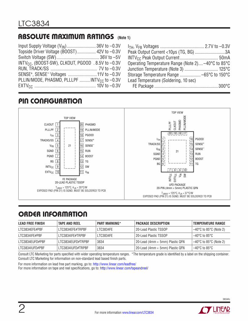
ABSOLUTE MAXIMUM RATINGSInput Supply Voltage (VIN) ......................... 36V to –0.3VTopside Driver Voltage (BOOST) ................ 42V to –0.3VSwitch Voltage (SW) ..................................... 36V to –5V INTVCC, (BOOST-SW), CLKOUT, PGOOD . 8.5V to –0.3VRUN, TRACK/SS ........................................ 7V to –0.3VSENSE+, SENSE– Voltages .........................11V to –0.3VPLLIN/MODE, PHASMD, PLLLPF ......... INTVCC to –0.3VEXTVCC ..................................................... 10V to –0.3V
(Note 1)
FE PACKAGE20-LEAD PLASTIC TSSOP
1
2
3
4
5
6
7
8
9
10
TOP VIEW
20
19
18
17
16
15
14
13
12
11
CLKOUT
PLLLPF
ITH
TRACKS/SS
VFB
SGND
PGND
BG
INTVCC
EXTVCC
PHASMD
PLLIN/MODE
PGOOD
SENSE+
SENSE–
RUN
BOOST
TG
SW
VIN
21
TJMAX = 125°C, θJA = 35°C/W
EXPOSED PAD (PIN 21) IS SGND, MUST BE SOLDERED TO PCB
20 19 18 17
7 8
TOP VIEW
UFD PACKAGE20-PIN (4mm × 5mm) PLASTIC QFN
9 10
6
5
4
3
2
1
11
12
13
14
15
16ITH
TRACK/SS
VFB
SGND
PGND
BG
PGOOD
SENSE+
SENSE–
RUN
BOOST
TG
PLLL
PF
CLKO
UT
PHAS
MD
PLLI
N/M
ODE
INTV
CC
EXTV
CC V IN
SW
21
TJMAX = 125°C, θJA = 37°C/W
EXPOSED PAD (PIN 21) IS SGND, MUST BE SOLDERED TO PCB
PIN CONFIGURATION
ORDER INFORMATIONLEAD FREE FINISH TAPE AND REEL PART MARKING* PACKAGE DESCRIPTION TEMPERATURE RANGE
LTC3834EFE#PBF LTC3834EFE#TRPBF LTC3834FE 20-Lead Plastic TSSOP –40°C to 85°C (Note 2)
LTC3834IFE#PBF LTC3834IFE#TRPBF LTC3834FE 20-Lead Plastic TSSOP –40°C to 85°C
LTC3834EUFD#PBF LTC3834EUFD#TRPBF 3834 20-Lead (4mm × 5mm) Plastic QFN –40°C to 85°C (Note 2)
LTC3834IUFD#PBF LTC3834IUFD#TRPBF 3834 20-Lead (4mm × 5mm) Plastic QFN –40°C to 85°C
Consult LTC Marketing for parts specified with wider operating temperature ranges. *The temperature grade is identified by a label on the shipping container.Consult LTC Marketing for information on non-standard lead based finish parts.For more information on lead free part marking, go to: http://www.linear.com/leadfree/ For more information on tape and reel specifications, go to: http://www.linear.com/tapeandreel/
ITH, VFB Voltages ...................................... 2.7V to –0.3VPeak Output Current <10µs (TG, BG) ..........................3AINTVCC Peak Output Current ................................. 50mAOperating Temperature Range (Note 2)....–40°C to 85°CJunction Temperature (Note 3) ............................. 125°CStorage Temperature Range .................. –65°C to 150°CLead Temperature (Soldering, 10 sec) FE Package ....................................................... 300°C
LTC3834
33834fc
For more information www.linear.com/LTC3834
ELECTRICAL CHARACTERISTICS The l denotes the specifications which apply over the full operating temperature range, otherwise specifications are at TA = 25°C. VIN = 12V, VRUN = 5V unless otherwise noted.
SYMBOL PARAMETER CONDITIONS MIN TYP MAX UNITS
Main Control Loops
VFB Regulated Feedback Voltage (Note 4); ITH Voltage = 1.2V l 0.792 0.800 0.808 V
IVFB Feedback Current (Note 4) –5 –50 nA
VREFLNREG Reference Voltage Line Regulation VIN = 4V to 30V (Note 4) 0.002 0.02 %/V
VLOADREG Output Voltage Load Regulation (Note 4) Measured in Servo Loop; ∆ITH Voltage = 1.2V to 0.7V Measured in Servo Loop; ∆ITH Voltage = 1.2V to 2V
l
l
0.1 –0.1
0.5 –0.5
% %
gm Transconductance Amplifier gm ITH = 1.2V; Sink/Source 5µA (Note 4) 0.5 mmho
IQ Input DC Supply Current Sleep Mode Shutdown
(Note 5) RUN = 5V, VFB = 0.83V (No Load) VRUN = 0V
30 4
50 10
µA µA
UVLO Undervoltage Lockout VIN Ramping Down l 3.7 4 V
VOVL Feedback Overvoltage Lockout Measured at VFB Relative to Regulated VFB 8 10 12 %
ISENSE Sense Pins Total Source Current VSENSE– = VSENSE
+ = 0V –220 µA
DFMAX Maximum Duty Factor In Dropout 98 99.4 %
ITRACK/SS Soft-Start Charge Current VTRACK = 0V 0.85 1.1 1.45 µA
VRUN ON RUN Pin ON Threshold VRUN Rising 0.5 0.7 0.9 V
VSENSE(MAX) Maximum Current Sense Threshold VFB = 0.7V, VSENSE– = 3.3V l 85 100 115 mV
TG tr TG tf
TG Transition Time: Rise Time Fall Time
(Note 6) CLOAD = 3300pF CLOAD = 3300pF
50 50
90 90
ns ns
BG tr BG tf
BG Transition Time: Rise Time Fall Time
(Note 6) CLOAD = 3300pF CLOAD = 3300pF
40 40
90 80
ns ns
TG/BG t1D Top Gate Off to Bottom Gate On Delay Synchronous Switch-On Delay Time
CLOAD = 3300pF 70 ns
BG/TG t2D Bottom Gate Off to Top Gate On Delay Top Switch-On Delay Time
CLOAD = 3300pF 70 ns
tON(MIN) Minimum On-Time (Note 7) 200 ns
INTVCC Linear Regulator
VINTVCCVIN Internal VCC Voltage 8.5V < VIN < 30V, VEXTVCC = 0V 5 5.25 5.5 V
VLDOVIN INTVCC Load Regulation ICC = 0mA to 20mA, VEXTVCC = 0V 0.2 1.0 %
VINTVCCEXT Internal VCC Voltage VEXTVCC = 8.5V 7.2 7.5 7.8 V
VLDOEXT INTVCC Load Regulation ICC = 0mA to 20mA, VEXTVCC = 8.5V 0.2 1.0 %
VEXTVCC EXTVCC Switchover Voltage EXTVCC Ramping Positive 4.5 4.7 V
VLDOHYS EXTVCC Hysteresis 0.2 V
Oscillator and Phase-Locked Loop
fNOM Nominal Frequency VPLLLPF = No Connect 360 400 440 kHz
fLOW Lowest Frequency VPLLLPF = 0V 220 250 280 kHz
fHIGH Highest Frequency VPLLLPF = INTVCC 475 530 580 kHz
fSYNCMIN Minimum Synchronizable Frequency PLLIN/MODE = External Clock; VPLLLPF = 0V 115 140 kHz
fSYNCMAX Maximum Synchronizable Frequency PLLIN/MODE = External Clock; VPLLLPF = 2V 650 800 kHz
IPLLLPF Phase Detector Output Current Sinking Capability Sourcing Capability
fPLLIN/MODE < fOSC fPLLIN/MODE > fOSC
–5 5
µA µA
LTC3834
43834fc
For more information www.linear.com/LTC3834
ELECTRICAL CHARACTERISTICS The l denotes the specifications which apply over the full operating temperature range, otherwise specifications are at TA = 25°C. VIN = 12V, VRUN = 5V unless otherwise noted.
SYMBOL PARAMETER CONDITIONS MIN TYP MAX UNITS
PGOOD Output
VPGL PGOOD Voltage Low IPGOOD = 2mA 0.1 0.3 V
IPGOOD PGOOD Leakage Current VPGOOD = 5V ±1 µA
VPG PGOOD Trip Level VFB with Respect to Set Regulated Voltage VFB Ramping Negative VFB Ramping Positive
–12 8
–10 10
–8 12
% %
Note 1: Stresses beyond those listed under Absolute Maximum Ratings may cause permanent damage to the device. Exposure to any Absolute Maximum Rating condition for extended periods may affect device reliability and lifetime.Note 2: The LTC3834E is guaranteed to meet performance specifications from 0°C to 85°C. Specifications over the –40°C to 85°C operating temperature range are assured by design, characterization and correlation with statistical process controls. The LTC3834I is guaranteed to meet performance specifications over the –40°C to 85°C operating temperature range.Note 3: TJ is calculated from the ambient temperature TA and power dissipation PD according to the following formulas: LTC3834FE: TJ = TA + (PD • 35°C/W) LTC3834UFD: TJ = TA + (PD • 37°C/W)
Note 4: The LTC3834 is tested in a feedback loop that servos VITH to a specified voltage and measures the resultant VFB.Note 5: Dynamic supply current is higher due to the gate charge being delivered at the switching frequency. See Applications Information.Note 6: Rise and fall times are measured using 10% and 90% levels. Delay times are measured using 50% levels.Note 7: The minimum on-time condition is specified for an inductor peak-to-peak ripple current ≥40% of IMAX (see Minimum On-Time Considerations in the Applications Information section).
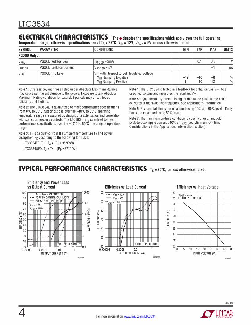
TYPICAL PERFORMANCE CHARACTERISTICS TA = 25°C, unless otherwise noted.
Efficiency and Power Loss vs Output Current Efficiency vs Load Current
OUTPUT CURRENT (A)
EFFI
CIEN
CY (%
)
POWER LOSS (m
W)
0.0001 0.01 1
3834 G01
0.000001
1
10
1000
100
0.1
10000
40
50
60
70
80
30
20
10
0
90
100 Burst Mode OPERATIONFORCED CONTINUOUS MODEPULSE SKIPPING MODE
VIN = 12VVOUT = 3.3V
FIGURE 11 CIRCUIT
Efficiency vs Input Voltage
OUTPUT CURRENT (A)
EFFI
CIEN
CY (%
)
0.0001 0.01 1
3834 G02
0.00000140
50
60
70
80
90
100VIN = 12VVIN = 5V
FIGURE 11 CIRCUIT
VOUT = 3.3V
INPUT VOLTAGE (V)
88
90
94
96
98
5 15
3834 G03
86
84
0 10 20 4025 30 35
82
80
92
EFFI
CIEN
CY (%
)
VOUT = 3.3VFIGURE 11 CIRCUIT
LTC3834
53834fc
For more information www.linear.com/LTC3834
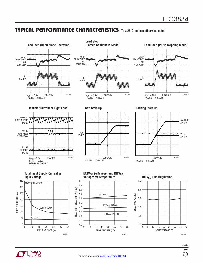
TYPICAL PERFORMANCE CHARACTERISTICS
Load Step (Burst Mode Operation)Load Step (Forced Continuous Mode) Load Step (Pulse Skipping Mode)
Inductor Current at Light Load Soft Start-Up Tracking Start-Up
Total Input Supply Current vs Input Voltage
EXTVCC Switchover and INTVCC Voltages vs Temperature INTVCC Line Regulation
TA = 25°C, unless otherwise noted.
VOUT = 3.3VFIGURE 11 CIRCUIT
VOUT100mV/DIV
ACCOUPLED
3834 G0420µs/DIV
IL2A/DIV
VOUT = 3.3VFIGURE 11 CIRCUIT
VOUT100mV/DIV
ACCOUPLED
3834 G0520µs/DIV
IL2A/DIV
VOUT = 3.3VFIGURE 11 CIRCUIT
VOUT100mV/DIV
ACCOUPLED
3834 G0620µs/DIV
IL2A/DIV
VOUT = 3.3VILOAD = 100µAFIGURE 11 CIRCUIT
FORCEDCONTINUOUS
MODE
3834 G072µs/DIV
2A/DIVBurst ModeOPERATION
PULSESKIPPING
MODE
3834 G0820ms/DIVFIGURE 11 CIRCUIT
VOUT1V/DIV
3834 G0920ms/DIVFIGURE 11 CIRCUIT
MASTER2V/DIV
VOUT2V/DIV
INPUT VOLTAGE (V)
200
250
25
3834 G10
100
150
105 15 20 30 35
50
0
300
350
SUPP
LY C
URRE
NT (µ
A)
300µA LOAD
NO LOAD
FIGURE 11 CIRCUIT
TEMPERATURE (°C)
4.8
5.0
5.4
5.6
5.8
6.0
55
3834 G11
4.6
4.4
–5–25–45 15 35 75 95
4.2
4.0
5.2
EXTV
CC A
ND IN
TVCC
VOL
TAGE
(V)
INTVCC
EXTVCC RISING
EXTVCC FALLING
INPUT VOLTAGE (V)
5.2
5.4
5.5
30
3834 G12
5.1
151050 20 25 35 405.0
5.3
INTV
CC V
OLTA
GE (V
)
LTC3834
63834fc
For more information www.linear.com/LTC3834
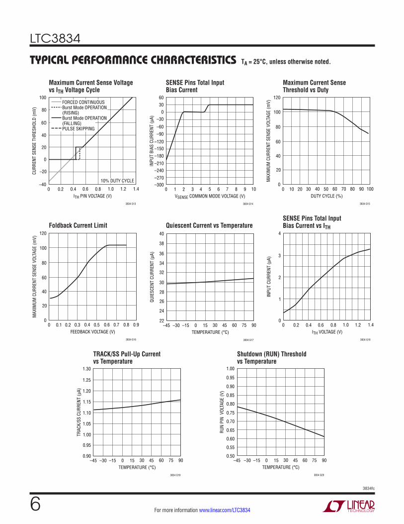
Maximum Current Sense Voltage vs ITH Voltage Cycle
SENSE Pins Total Input Bias Current
Maximum Current Sense Threshold vs Duty
Foldback Current Limit Quiescent Current vs TemperatureSENSE Pins Total Input Bias Current vs ITH
TRACK/SS Pull-Up Current vs Temperature
Shutdown (RUN) Threshold vs Temperature
TYPICAL PERFORMANCE CHARACTERISTICS TA = 25°C, unless otherwise noted.
ITH PIN VOLTAGE (V)
40
6O
100
0.4 0.8
3834 G13
20
0
0 0.2 0.6 1.0 1.2 1.4
–20
–40
80
CURR
ENT
SENS
E TH
RESH
OLD
(mV)
10% DUTY CYCLE
FORCED CONTINUOUSBurst Mode OPERATION(RISING)Burst Mode OPERATION(FALLING)PULSE SKIPPING
VSENSE COMMON MODE VOLTAGE (V)
–120–150
–180
–210–240
30
0–30
–60
–90
60
6 7 8 9
3834 G14
–270
3210 4 5 10–300
INPU
T BI
AS C
URRE
NT (µ
A)
DUTY CYCLE (%)
80
120
30 50
3834 G15
60
40
100 20 40 60 10070 80 90
20
0
100
MAX
IMUM
CUR
RENT
SEN
SE V
OLTA
GE (m
V)
FEEDBACK VOLTAGE (V)0
80
120
0.3 0.5
3834 G16
60
40
0.1 0.2 0.4 0.6 0.90.7 0.8
20
0
100
MAX
IMUM
CUR
RENT
SEN
SE V
OLTA
GE (m
V)
TEMPERATURE (°C)
30
32
36
38
40
45
3834 G17
28
26
0–15–30–45 15 30 60 75 90
24
22
34
QUIE
SCEN
T CU
RREN
T (µ
A)
ITH VOLTAGE (V)
2
3
4
1.2
3834 G18
1
0.60.40.20 0.8 1.0 1.40
INPU
T CU
RREN
T (µ
A)
TEMPERATURE (°C)
1.05
1.10
1.20
1.25
1.30
45
3834 G19
1.00
0.95
0–15–30–45 15 30 60 75 900.90
1.15
TRAC
K/SS
CUR
RENT
(µA)
TEMPERATURE (°C)
0.80
0.75
0.70
0.65
0.60
0.55
0.50
1.00
0.95
0.90
0.85
45 60 75 90
3834 G20
0–15–30–45 15 30
RUN
PIN
VOL
TAGE
(V)
LTC3834
73834fc
For more information www.linear.com/LTC3834
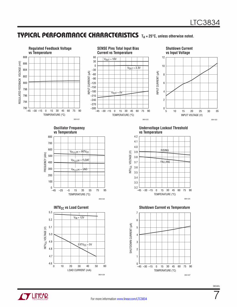
Regulated Feedback Voltage vs Temperature
SENSE Pins Total Input Bias Current vs Temperature
Shutdown Current vs Input Voltage
Oscillator Frequency vs Temperature
Undervoltage Lockout Threshold vs Temperature
INTVCC vs Load Current Shutdown Current vs Temperature
TYPICAL PERFORMANCE CHARACTERISTICS TA = 25°C, unless otherwise noted.
TEMPERATURE (°C)
800
798
796
794
792
808
806
804
802
45 60 75 90
3834 G21
0–15–30–45 15 30
REGU
LATE
D FE
EDBA
CK V
OLTA
GE (m
V)
TEMPERATURE (°C)
–120–150
–180
–210–240
30
0–30
–60
–90
60
45 60 75 90
3834 G22
–270
0–15–30–45 15 30–300
INPU
T CU
RREN
T (µ
A)
VOUT = 10V
VOUT = 3.3V
VOUT = 0V
INPUT VOLTAGE (V)
8
10
35
3834 G23
6
4
2015105 25 30
2
0
12
INPU
T CU
RREN
T (µ
A)
TEMPERATURE (°C)
400
500
700
800
55
3834 G24
300
200
–5–25–45 15 35 75 95
100
0
600
FREQ
UENC
Y (k
Hz) VPLLLPF = INTVCC
VPLLLPF = FLOAT
VPLLLPF = GND
TEMPERATURE (°C)
3.6
3.5
3.4
3.3
3.2
4.1
4.0
3.9
3.8
3.7
4.2
45 60 75 90
3834 G25
0–15–30–45 15 30
INTV
CC V
OLTA
GE (V
) RISING
FALLING
LOAD CURRENT (mA)
5.0
5.2
5.3
50
3834 G26
4.9
4.8
20100 30 40 60
4.7
4.6
5.1
INTV
CC V
OLTA
GE (V
)
EXTVCC = 5V
VIN = 12V
TEMPERATURE (°C)
4
5
7
45
3834 G27
3
2
0–15–30–45 15 30 60 75 90
1
0
6
SHUT
DOW
N CU
RREN
T (µ
A)
LTC3834
83834fc
For more information www.linear.com/LTC3834
PIN FUNCTIONS (FE/UFD)
CLKOUT (Pin 1/Pin 19): Open-Drain Output Clock Signal available to daisy-chain other controller ICs for additional MOSFET driver stages/phases.
PLLLPF (Pin 2/Pin 20): The phase-locked loop’s lowpass filter is tied to this pin when synchronizing to an external clock. Alternatively, tie this pin to GND, INTVCC or leave floating to select 250kHz, 530kHz or 400kHz switching frequency.
ITH (Pin 3/Pin 1): Error Amplifier Outputs and Switching Regulator Compensation Points. The current comparator trip point increases with this control voltage.
TRACK/SS (Pin 4/Pin 2): External Tracking and Soft-Start Input. The LTC3834 regulates the VFB voltage to the smaller of 0.8V or the voltage on the TRACK/SS pin. A internal 1µA pull-up current source is connected to this pin. A capacitor to ground at this pin sets the ramp time to final regulated output voltage. Alternatively, a resistor divider on another voltage supply connected to this pin allows the LTC3834 output to track the other supply during start-up.
VFB (Pin 5/Pin 3): Receives the remotely sensed feedback voltage from an external resistive divider across the output.
SGND (Pin 6/Pin 4): Small-Signal Ground. Must be routed separately from high current grounds to the common (–) terminals of the input capacitor.
PGND (Pin 7/Pin 5): Driver Power Ground. Connects to the source of bottom (synchronous) N-channel MOSFET, anode of the Schottky rectifier and the (–) terminal of CIN.
BG (Pin 8/Pin 6): High Current Gate Drive for Bottom (Synchronous) N-Channel MOSFET. Voltage swing at this pin is from ground to INTVCC.
INTVCC (Pin 9/Pin 7): Output of the Internal Linear Low Dropout Regulator. The driver and control circuit are powered from this voltage source. Must be decoupled to power ground with a minimum of 4.7µF tantalum or ceramic capacitor.
EXTVCC (Pin 10/Pin 8): External Power Input to an Internal LDO Connected to INTVCC. This LDO supplies VCC power, bypassing the internal LDO powered from VIN whenever EXTVCC is higher than 4.7V. See EXTVCC Connection in
the Applications Information section. Do not exceed 10V on this pin.
VIN (Pin 11/Pin 9): Main Supply Pin. A bypass capacitor should be tied between this pin and the signal ground pin.
SW (Pin 12/Pin 10): Switch Node Connections to Inductor. Voltage swing at this pin is from a Schottky diode (external) voltage drop below ground to VIN.
TG (Pin 13/Pin 11): High Current Gate Drive for Top N-Channel MOSFET. These are the outputs of floating drivers with a voltage swing equal to INTVCC – 0.5V su-perimposed on the switch node voltage SW.
BOOST (Pin 14/Pin 12): Bootstrapped Supply to the Topside Floating Driver. A capacitor is connected between the BOOST and SW pins and a Schottky diode is tied between the BOOST and INTVCC pins. Voltage swing at the BOOST pin is from INTVCC to (VIN + INTVCC).
RUN (Pin 15/Pin 13): Digital Run Control Input for Controller. Forcing this pin below 0.7V shuts down all controller functions, reducing the quiescent current that the LTC3834 draws to approximately 4µA.
SENSE– (Pin 16/Pin 14): The (–) Input to the Differential Current Comparator.
SENSE+ (Pin 17/Pin 15): The (+) Input to the Differential Current Comparator. The ITH pin voltage and controlled offsets between the SENSE– and SENSE+ pins in conjunc-tion with RSENSE set the current trip threshold.
PGOOD (Pin 18/Pin 16): Open-Drain Logic Output. PGOOD is pulled to ground when the voltage on the VFB pin is not within ±10% of its set point.
PLLIN/MODE (Pin 19/Pin 17): External Synchronization Input to Phase Detector and Forced Continuous Control Input. When an external clock is applied to this pin, the phase-locked loop will force the rising TG signal to be synchronized with the rising edge of the external clock. In this case, an R-C filter must be connected to the PLLLPF pin. When not synchronizing to an external clock, this input determines how the LTC3834 operates at light loads. Pulling this pin below 0.7V selects Burst Mode operation. Tying this pin to INTVCC forces continuous inductor current

LTC3834
93834fc
For more information www.linear.com/LTC3834
FUNCTIONAL DIAGRAM
PIN FUNCTIONS (FE/UFD)
operation. Tying this pin to a voltage greater than 0.9V and less than INTVCC selects pulse-skipping operation.
PHASMD (Pin 20/Pin 18): Control Input to Phase Selector which determines the phase relationships between TG and the CLKOUT signal.
Exposed Pad (Pin 21/Pin 21): SGND. Must be soldered to the PCB.
SWITCHLOGIC
+
–
4.7V
VIN
VIN
INTVCC – 0.5V
INTVCC
0.8V
FC
10k
BURSTEN
CLK
+
–
+
–
–
+
–
+
INTERNALSUPPLY
RLP
CLP
PLLIN/MODE
EXTVCC
INTVCC
SGND
+
5.25V/7.5VLDO
SW
SHDN
SLEEP0.4V
TOP
BOOST
TG CB
CIND
DB
PGND
BOTBG
INTVCC
INTVCC
VIN
COUT
VOUT
3834 FD
RSENSE
RBVFB
DROPOUTDET BOT
TOP ONS
R
Q
Q
OSCILLATOR
PHASE DET
PLLLPF
PLLIN/MODE
FC
BURSTEN
EA
0.88V
0.80VTRACK/SS
OV
VFB
0.5µA
1µA6V
RA
–
+
RC
TRACK/SS
ITHCC
CC2
CSS
2(VFB)0.45V
SLOPECOMP
6mV
+
–
–
+
SENSE–
SENSE+
ICMP IR
B
RUN
+– –+
PHASMD
CLKOUT
FIN
+
–
+
–PGOOD VFB1
0.88V
0.72V
L
SHDN
LTC3834
103834fc
For more information www.linear.com/LTC3834
OPERATION (Refer to Functional Diagram)
Main Control Loop
The LTC3834 uses a constant-frequency, current mode step-down architecture. During normal operation, the ex-ternal top MOSFET is turned on when the clock sets the RS latch, and is turned off when the main current comparator, ICMP, resets the RS latch. The peak inductor current at which ICMP trips and resets the latch is controlled by the voltage on the ITH pin, which is the output of the error am-plifier EA. The error amplifier compares the output voltage feedback signal at the VFB pin, (which is generated with an external resistor divider connected across the output voltage, VOUT , to ground) to the internal 0.800V reference voltage. When the load current increases, it causes a slight decrease in VFB relative to the reference, which cause the EA to increase the ITH voltage until the average inductor current matches the new load current.
After the top MOSFET is turned off each cycle, the bottom MOSFET is turned on until either the inductor current starts to reverse, as indicated by the current comparator IR, or the beginning of the next clock cycle.
INTVCC/EXTVCC Power
Power for the top and bottom MOSFET drivers and most other internal circuitry is derived from the INTVCC pin. When the EXTVCC pin is left open or tied to a voltage less than 4.7V, an internal 5.25V low dropout linear regulator supplies INTVCC power from VIN. If EXTVCC is taken above 4.7V, the 5.25V regulator is turned off and a 7.5V low dropout linear regulator is enabled that supplies INTVCC power from EXTVCC. If EXTVCC is less than 7.5V (but greater than 4.7V), the 7.5V regulator is in dropout and INTVCC is approximately equal to EXTVCC. When EXTVCC is greater than 7.5V (up to an absolute maximum rating of 10V), INTVCC is regulated to 7.5V. Using the EXTVCC pin allows the INTVCC power to be derived from a high efficiency external source such as one of the LTC3834 switching regulator outputs.
The top MOSFET driver is biased from the floating bootstrap capacitor, CB, which normally recharges during each off cycle through an external diode when the top MOSFET turns off. If the input voltage VIN decreases to a voltage close to VOUT , the loop may enter dropout and attempt to turn on the top MOSFET continuously. The dropout detector detects this and forces the top MOSFET off for about one twelfth of the clock period every tenth cycle to allow CB to recharge.
Shutdown and Start-Up (RUN and TRACK/SS Pins)
The LTC3834 can be shut down using the RUN pin. Pulling this pin below 0.7V shuts down the main control loop of the controller. A low disables the controller and most internal circuits, including the INTVCC regulator, at which time the LTC3834 draws only 4µA of quiescent current.
Releasing the RUN pin allows an internal 0.5µA current to pull up the pin and enable that controller. Alternatively, the RUN pin may be externally pulled up or driven directly by logic. Be careful not to exceed the Absolute Maximum rating of 7V on this pin.
The start-up of the output voltage VOUT is controlled by the voltage on the TRACK/SS pin. When the voltage on the TRACK/SS pin is less than the 0.8V internal reference, the LTC3834 regulates the VFB voltage to the TRACK/SS pin voltage instead of the 0.8V reference. This allows the TRACK/SS pin to be used to program a soft-start by connecting an external capacitor from the TRACK/SS pin to SGND. An internal 1µA pull-up current charges this capacitor creating a voltage ramp on the TRACK/SS pin. As the TRACK/SS voltage rises linearly from 0V to 0.8V (and beyond), the output voltage VOUT rises smoothly from zero to its final value.
Alternatively the TRACK/SS pin can be used to cause the start-up of VOUT to “track” that of another supply. Typ-ically, this requires connecting to the TRACK/SS pin an external resistor divider from the other supply to ground (see Applications Information section).

LTC3834
113834fc
For more information www.linear.com/LTC3834
OPERATION (Refer to Functional Diagram)
When the RUN pin is pulled low to disable the LTC3834, or when VIN drops below its undervoltage lockout threshold of 3.7V, the TRACK/SS pin is pulled low by an internal MOSFET. When in undervoltage lockout, the controller is disabled and the external MOSFETs are held off.
Light Load Current Operation (Burst Mode Operation, Pulse-Skipping or Continuous Conduction) (PLLIN/MODE Pin)
The LTC3834 can be enabled to enter high efficiency Burst Mode operation, constant-frequency pulse-skipping mode, or forced continuous conduction mode at low load currents. To select Burst Mode operation, tie the PLLIN/MODE pin to a DC voltage below 0.8V (e.g., SGND). To select forced continuous operation, tie the PLLIN/MODE pin to INTVCC. To select pulse skipping mode, tie the PLLIN/MODE pin to a DC voltage greater than 0.8V and less than INTVCC – 0.5V.
When the LTC3834 is enabled for Burst Mode operation, the peak current in the inductor is set to approximately one-tenth of the maximum sense voltage even though the voltage on the ITH pin indicates a lower value. If the average inductor current is lower than the load current, the error amplifier EA will decrease the voltage on the ITH pin. When the ITH voltage drops below 0.4V, the internal sleep signal goes high (enabling “sleep” mode) and both external MOSFETs are turned off. The ITH pin is then disconnected from the output of the EA and “parked” at 0.425V.
In sleep mode, much of the internal circuitry is turned off, reducing the quiescent current that the LTC3834 draws to only 30µA. In sleep mode, the load current is supplied by the output capacitor. As the output voltage decreases, the EA’s output begins to rise. When the output voltage drops enough, the ITH pin is reconnected to the output of the EA, the sleep signal goes low, and the controller
resumes normal operation by turning on the top external MOSFET on the next cycle of the internal oscillator.
When the LTC3834 is enabled for Burst Mode operation, the inductor current is not allowed to reverse. The reverse current comparator (RICMP) turns off the bottom external MOSFET just before the inductor current reaches zero, preventing it from reversing and going negative, thus operating in discontinuous operation.
In forced continuous operation, the inductor current is allowed to reverse at light loads or under large transient conditions. The peak inductor current is determined by the voltage on the ITH pin, just as in normal operation. In this mode, the efficiency at light loads is lower than in Burst Mode operation. However, continuous operation has the advantages of lower output ripple and less interference to audio circuitry. In forced continuous mode, the output ripple is independent of load current.
When the PLLIN/MODE pin is connected for pulse skip-ping mode or clocked by an external clock source to use the phase-locked loop (see Frequency Selection and Phase-Locked Loop section), the LTC3834 operates in PWM pulse skipping mode at light loads. In this mode, constant-frequency operation is maintained down to approximately 1% of designed maximum output current. At very light loads, the current comparator ICMP may re-main tripped for several cycles and force the external top MOSFET to stay off for the same number of cycles (i.e., skipping pulses). The inductor current is not allowed to reverse (discontinuous operation). This mode, like forced continuous operation, exhibits low output ripple as well as low audio noise and reduced RF interference as compared to Burst Mode operation. It provides higher low current efficiency than forced continuous mode, but not nearly as high as Burst Mode operation.
LTC3834
123834fc
For more information www.linear.com/LTC3834
OPERATIONFrequency Selection and Phase-Locked Loop (PLLLPF and PLLIN/MODE Pins)
The selection of switching frequency is a trade-off between efficiency and component size. Low frequency operation increases efficiency by reducing MOSFET switching loss-es, but requires larger inductance and/or capacitance to maintain low output ripple voltage.
The switching frequency of the LTC3834’s controllers can be selected using the PLLLPF pin.
If the PLLIN/MODE pin is not being driven by an exter-nal clock source, the PLLLPF pin can be floated, tied to INTVCC, or tied to SGND to select 400kHz, 530kHz or 250kHz, respectively.
A phase-locked loop (PLL) is available on the LTC3834 to synchronize the internal oscillator to an external clock source that is connected to the PLLIN/MODE pin. In this case, a series R-C should be connected between the PLLLPF pin and SGND to serve as the PLL’s loop filter. The LTC3834 phase detector adjusts the voltage on the PLLLPF pin to align the turn-on of the external top MOSFET to the rising edge of the synchronizing signal.
The typical capture range of the LTC3834’s phase-locked loop is from approximately 115kHz to 800kHz, with a guarantee to be between 140kHz and 650kHz. In other words, the LTC3834’s PLL is guaranteed to lock to an external clock source whose frequency is between 140kHz and 650kHz.
The typical input clock thresholds on the PLLIN/MODE pin are 1.6V (rising) and 1.2V (falling).
PolyPhase Applications (CLKOUT and PHASMD Pins)
The LTC3834 features two pins (CLKOUT and PHASMD) that allow other controller ICs to be daisy-chained with the LTC3834 in PolyPhase applications. The clock output
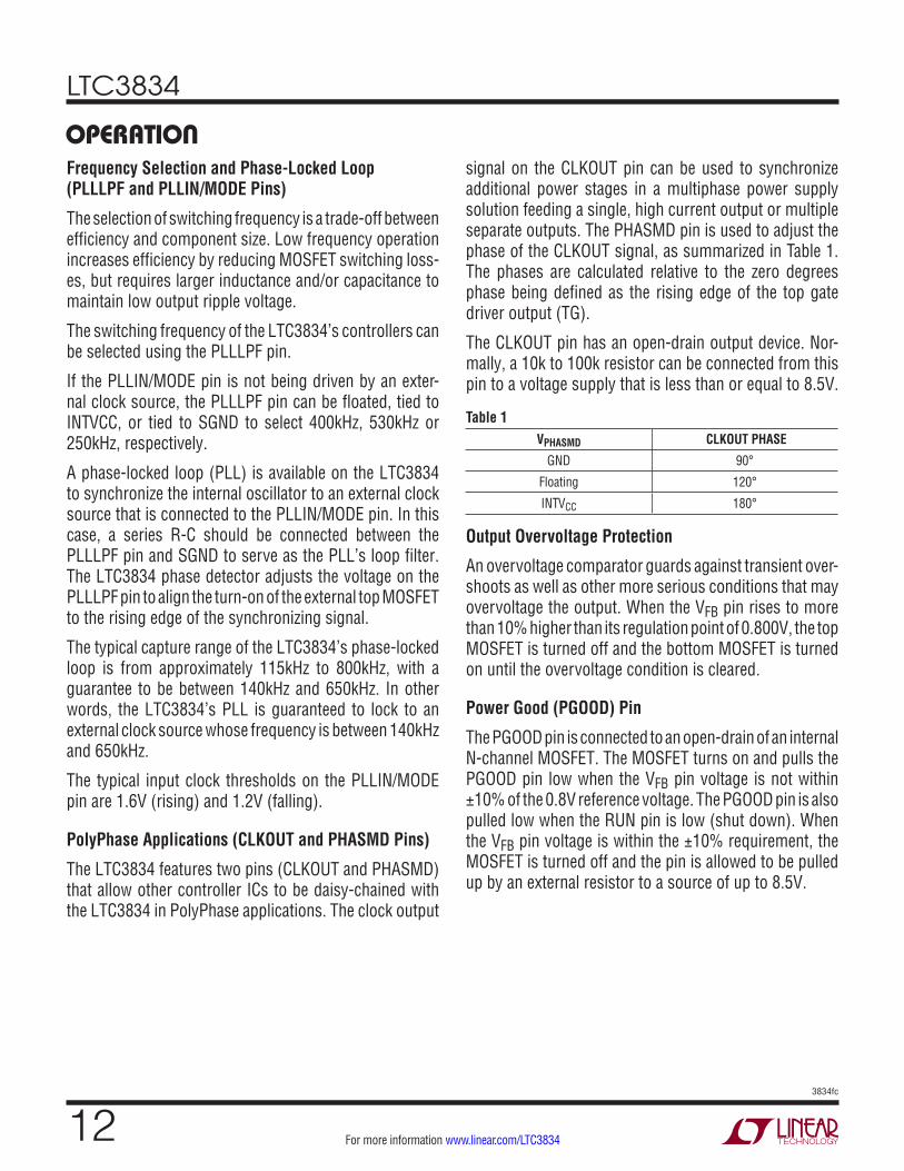
signal on the CLKOUT pin can be used to synchronize additional power stages in a multiphase power supply solution feeding a single, high current output or multiple separate outputs. The PHASMD pin is used to adjust the phase of the CLKOUT signal, as summarized in Table 1. The phases are calculated relative to the zero degrees phase being defined as the rising edge of the top gate driver output (TG).
The CLKOUT pin has an open-drain output device. Nor-mally, a 10k to 100k resistor can be connected from this pin to a voltage supply that is less than or equal to 8.5V.
Table 1VPHASMD CLKOUT PHASE
GND 90°
Floating 120°
INTVCC 180°
Output Overvoltage Protection
An overvoltage comparator guards against transient over-shoots as well as other more serious conditions that may overvoltage the output. When the VFB pin rises to more than 10% higher than its regulation point of 0.800V, the top MOSFET is turned off and the bottom MOSFET is turned on until the overvoltage condition is cleared.
Power Good (PGOOD) Pin
The PGOOD pin is connected to an open-drain of an internal N-channel MOSFET. The MOSFET turns on and pulls the PGOOD pin low when the VFB pin voltage is not within ±10% of the 0.8V reference voltage. The PGOOD pin is also pulled low when the RUN pin is low (shut down). When the VFB pin voltage is within the ±10% requirement, the MOSFET is turned off and the pin is allowed to be pulled up by an external resistor to a source of up to 8.5V.
LTC3834
133834fc
For more information www.linear.com/LTC3834
RSENSE Selection For Output Current
RSENSE is chosen based on the required output current. The current comparator has a maximum threshold of 100mV/RSENSE and an input common mode range of SGND to 10V. The current comparator threshold sets the peak of the inductor current, yielding a maximum average output current IMAX equal to the peak value less half the peak-to-peak ripple current, ∆IL.
Allowing a margin for variations in the IC and external component values yields:
RSENSE =
80mVIMAX
When using the controller in very low dropout conditions, the maximum output current level will be reduced due to the internal compensation required to meet stability criterion for buck regulators operating at greater than 50% duty factor. A curve is provided to estimate this reduction in peak output current level depending upon the operating duty factor.
Operating Frequency and Synchronization
The choice of operating frequency, is a trade-off between efficiency and component size. Low frequency operation improves efficiency by reducing MOSFET switching losses, both gate charge loss and transition loss. However, lower frequency operation requires more inductance for a given amount of ripple current.
The internal oscillator of the LTC3834 runs at a nominal 400kHz frequency when the PLLLPF pin is left floating and the PLLIN/MODE pin is a DC low or high. Pulling the PLLLPF to INTVCC selects 530kHz operation; pulling the PLLLPF to SGND selects 250kHz operation.
Alternatively, the LTC3834 will phase-lock to a clock signal applied to the PLLIN/MODE pin with a frequency between 140kHz and 650kHz (see Phase-Locked Loop and Frequency Synchronization).
Inductor Value Calculation
The operating frequency and inductor selection are inter-related in that higher operating frequencies allow the use of smaller inductor and capacitor values. So why would
APPLICATIONS INFORMATIONanyone ever choose to operate at lower frequencies with larger components? The answer is efficiency. A higher frequency generally results in lower efficiency because of MOSFET gate charge losses. In addition to this basic trade-off, the effect of inductor value on ripple current and low current operation must also be considered.
The inductor value has a direct effect on ripple current. The inductor ripple current ∆IL decreases with higher inductance or frequency and increases with higher VIN:
∆IL =
1(f)(L)
VOUT 1–VOUT
VIN
Accepting larger values of ∆IL allows the use of low inductances, but results in higher output voltage ripple and greater core losses. A reasonable starting point for setting ripple current is ∆IL = 0.3(IMAX). The maximum ∆IL occurs at the maximum input voltage.
The inductor value also has secondary effects. The tran-sition to Burst Mode operation begins when the average inductor current required results in a peak current below 10% of the current limit determined by RSENSE. Lower inductor values (higher ∆IL) will cause this to occur at lower load currents, which can cause a dip in efficiency in the upper range of low current operation. In Burst Mode operation, lower inductance values will cause the burst frequency to decrease.
Inductor Core Selection
Once the value for L is known, the type of inductor must be selected. High efficiency converters generally cannot afford the core loss found in low cost powdered iron cores, forcing the use of more expensive ferrite or molypermalloy cores. Actual core loss is independent of core size for a fixed inductor value, but it is very dependent on inductance selected. As inductance increases, core losses go down. Unfortunately, increased inductance requires more turns of wire and therefore copper losses will increase.
Ferrite designs have very low core loss and are preferred at high switching frequencies, so design goals can con-centrate on copper loss and preventing saturation. Ferrite core material saturates “hard,” which means that induc-tance collapses abruptly when the peak design current is

LTC3834
143834fc
For more information www.linear.com/LTC3834
APPLICATIONS INFORMATIONexceeded. This results in an abrupt increase in inductor ripple current and consequent output voltage ripple. Do not allow the core to saturate!
Power MOSFET and Schottky Diode (Optional) Selection
Two external power MOSFETs must be selected for the LTC3834: one N-channel MOSFET for the top (main) switch, and one N-channel MOSFET for the bottom (syn-chronous) switch.
The peak-to-peak drive levels are set by the INTVCC voltage. This voltage is typically 5V during start-up (see EXTVCC Pin Connection). Consequently, logic-level threshold MOSFETs must be used in most applications. The only exception is if low input voltage is expected (VIN < 5V); then, sub-logic level threshold MOSFETs (VGS(TH) < 3V) should be used. Pay close attention to the BVDSS specification for the MOSFETs as well; most of the logic-level MOSFETs are limited to 30V or less.
Selection criteria for the power MOSFETs include the “ON” resistance RDS(ON), Miller capacitance CMILLER, input voltage and maximum output current. Miller capacitance, CMILLER, can be approximated from the gate charge curve usually provided on the MOSFET manufacturers’ data sheet. CMILLER is equal to the increase in gate charge along the horizontal axis while the curve is approximately flat divided by the specified change in VDS. This result is then multiplied by the ratio of the application applied VDS to the Gate charge curve specified VDS. When the IC is operating in continuous mode the duty cycles for the top and bottom MOSFETs are given by:
Main SwitchDuty Cycle =
VOUT
VIN
Synchronous SwitchDuty Cycle =
VIN – VOUT
VIN
The MOSFET power dissipations at maximum output current are given by:
PMAIN =VOUT
VIN
IMAX( )2 1+ δ∆T( )RDS(ON) +
VIN( )2 IMAX
2
RDR( ) CMILLER( ) •
1VINTVCC – VTHMIN
+1
VTHMIN
f( )
PSYNC =
VIN – VOUT
VIN
IMAX( )2 1+ δ∆T( )RDS(ON)
where δ is the temperature dependency of RDS(ON) and RDR (approximately 2Ω) is the effective driver resistance at the MOSFET ’s Miller threshold voltage. VTHMIN is the typical MOSFET minimum threshold voltage.
Both MOSFETs have I2R losses while the topside N-channel equation includes an additional term for transition losses, which are highest at high input voltages. For VIN < 20V the high current efficiency generally improves with larger MOSFETs, while for VIN > 20V the transition losses rapidly increase to the point that the use of a higher RDS(ON) device with lower CMILLER actually provides higher efficiency. The synchronous MOSFET losses are greatest at high input voltage when the top switch duty factor is low or during a short-circuit when the synchronous switch is on close to 100% of the period.
The term (1 + δ∆T) is generally given for a MOSFET in the form of a normalized RDS(ON) vs Temperature curve, but δ = 0.005/°C can be used as an approximation for low voltage MOSFETs.
The optional Schottky diode D1 shown in Figure 6 con-ducts during the dead-time between the conduction of the two power MOSFETs. This prevents the body diode of the bottom MOSFET from turning on, storing charge during the dead-time and requiring a reverse recovery period that could cost as much as 3% in efficiency at high VIN. A 1A to 3A Schottky is generally a good compromise for both regions of operation due to the relatively small average current. Larger diodes result in additional transition losses due to their larger junction capacitance.
LTC3834
153834fc
For more information www.linear.com/LTC3834
APPLICATIONS INFORMATIONCIN and COUT Selection
In continuous mode, the source current of the top MOSFET is a square wave of duty cycle (VOUT)/(VIN). To prevent large voltage transients, a low ESR capacitor sized for the maximum RMS current must be used. The maximum RMS capacitor current is given by:
CIN Required IRMS ≈
IMAX
VIN
VOUT( ) VIN – VOUT( )
1/2
This formula has a maximum at VIN = 2VOUT , where IRMS = IOUT/2. This simple worst-case condition is commonly used for design because even significant deviations do not offer much relief. Note that capacitor manufacturers’ ripple current ratings are often based on only 2000 hours of life. This makes it advisable to further derate the capacitor, or to choose a capacitor rated at a higher temperature than required. Several capacitors may be paralleled to meet size or height requirements in the design. Due to the high operating frequency of the LTC3834, ceramic capacitors can also be used for CIN. Always consult the manufacturer if there is any question.
The selection of COUT is driven by the effective series resistance (ESR). Typically, once the ESR requirement is satisfied, the capacitance is adequate for filtering. The output ripple (∆VOUT) is approximated by:
∆VOUT ≈ IRIPPLE ESR +
18fCOUT
where f is the operating frequency, COUT is the output ca-pacitance and IRIPPLE is the ripple current in the inductor. The output ripple is highest at maximum input voltage since IRIPPLE increases with input voltage.
Setting Output Voltage
The LTC3834 output voltage is set by an external feedback resistor divider carefully placed across the output, as shown in Figure 1. The regulated output voltage is determined by:
VOUT = 0.8V • 1+
RB
RA
To improve the frequency response, a feed-forward ca-pacitor, CFF , may be used. Great care should be taken to route the VFB line away from noise sources, such as the inductor and the SW line.
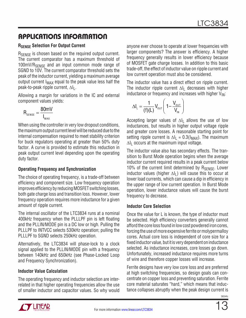
SENSE+ and SENSE– Pins
The common mode input range of the current comparator is from 0V to 10V. Continuous linear operation is provided throughout this range allowing output voltages from 0.8V to 10V. The input stage of the current comparator requires that current either be sourced or sunk from the SENSE pins depending on the output voltage, as shown in the curve in Figure 2. If the output voltage is below 1.5V, current will flow out of both SENSE pins to the main output. In these cases, the output can be easily pre-loaded by the VOUT resistor divider to compensate for the current comparator’s negative input bias current. Since VFB is servoed to the 0.8V reference voltage, RA in Figure 1 should be chosen to be less than 0.8V/ISENSE, with ISENSE determined from Figure 2 at the specified output voltage.
LTC3834
VFB
VOUT
RB CFF
RA
3834 F01
Figure 1. Setting Output Voltage
VSENSE COMMON MODE VOLTAGE (V)0
–700IN
PUT
CURR
ENT
(µA)
–600
–400
–300
–200
6 7 8 9
200
3835 F02
–500
1 2 3 4 5 10
–100
0
100
Figure 2. SENSE Pins Input Bias Current vs Common Mode Voltage
LTC3834
163834fc
For more information www.linear.com/LTC3834
APPLICATIONS INFORMATIONTracking and Soft-Start (TRACK/SS Pin)
The start-up of VOUT is controlled by the voltage on the TRACK/SS pin. When the voltage on the TRACK/SS pin is less than the internal 0.8V reference, the LTC3834 reg-ulates the VFB pin voltage to the voltage on the TRACK/SS pin instead of 0.8V. The TRACK/SS pin can be used to program an external soft-start function or to allow VOUT to “track” another supply during start-up.
Soft-start is enabled by simply connecting a capacitor from the TRACK/SS pin to ground, as shown in Figure 3. An internal 1µA current source charges up the capacitor, providing a linear ramping voltage at the TRACK/SS pin. The LTC3834 will regulate the VFB pin (and hence VOUT)
according to the voltage on the TRACK/SS pin, allowing VOUT to rise smoothly from 0V to its final regulated value. The total soft-start time will be approximately:
tSS = CSS •
0.8V1µA
Alternatively, the TRACK/SS pin can be used to track two (or more) supplies during start-up, as shown qualitatively in Figures 4a and 4b. To do this, a resistor divider should be connected from the master supply (VX) to the TRACK/SS pin of the slave supply (VOUT), as shown in Figure 5. During start-up VOUT will track VX according to the ratio set by the resistor divider:
VX
VOUT
=RA
RTRACKA
•RTRACKA +RTRACKB
RA +RB
For coincident tracking (VOUT = VX during start-up),
RA = RTRACKA
RB = RTRACKB
LTC3834TRACK/SS
CSS
SGND
3834 F03
Figure 3. Using the TRACK/SS Pin to Program Soft-Start
TIME
(4a) Coincident Tracking
VX (MASTER)
VOUT (SLAVE)
OUTP
UT V
OLTA
GE
3834 F04A
VX (MASTER)
VOUT (SLAVE)
TIME 3834 F04B
(4b) Ratiometric Tracking
OUTP
UT V
OLTA
GE
Figure 4. Two Different Modes of Output Voltage Tracking
LTC3834
VOUTVx
VFB
TRACK/SS
3834 F05
RB
RA
RTRACKA
RTRACKB
Figure 5. Using the TRACK/SS Pin for Tracking

LTC3834
173834fc
For more information www.linear.com/LTC3834
APPLICATIONS INFORMATIONINTVCC Regulators
The LTC3834 features two separate internal P-channel low dropout linear regulators (LDO) that supply power at the INTVCC pin from either the VIN supply pin or the EXTVCC pin, respectively, depending on the connection of the EXTVCC pin. INTVCC powers the gate drivers and much of the LTC3834’s internal circuitry. The VIN LDO regulates the voltage at the INTVCC pin to 5.25V and the EXTVCC LDO regulates it to 7.5V. Each of these can supply a peak current of 50mA and must be bypassed to ground with a minimum of 4.7µF ceramic capacitor. The ceramic capacitor placed directly adjacent to the INTVCC and PGND IC pins is highly recommended. Good bypassing is needed to supply the high transient currents required by the MOSFET gate drivers and to prevent interaction between the channels.
High input voltage applications in which large MOSFETs are being driven at high frequencies may cause the max-imum junction temperature rating for the LTC3834 to be exceeded. The INTVCC current, which is dominated by the gate charge current, may be supplied by either the 5V VIN LDO or the 7.5V EXTVCC LDO. When the voltage on the EXTVCC pin is less than 4.7V, the VIN LDO is enabled. Power dissipation for the IC in this case is highest and is equal to VIN • IINTVCC. The gate charge current is depen-dent on operating frequency as discussed in the Efficiency Considerations section. The junction temperature can be estimated by using the equations given in Note 3 of the Electrical Characteristics. For example, the LTC3834 INTVCC current is limited to less than 41mA from a 24V supply when in the G package and not using the EXTVCC supply:
TJ = 70°C + (41mA)(36V)(95°C/W) = 125°C
To prevent the maximum junction temperature from being exceeded, the input supply current must be checked while operating in continuous conduction mode (PLLIN/MODE = INTVCC) at maximum VIN.
When the voltage applied to EXTVCC rises above 4.7V, the VIN LDO is turned off and the EXTVCC LDO is enabled. The EXTVCC LDO remains on as long as the voltage applied to EXTVCC remains above 4.5V. The EXTVCC LDO attempts to regulate the INTVCC voltage to 7.5V, so while EXTVCC is less than 7.5V, the LDO is in dropout and the INTVCC voltage is approximately equal to EXTVCC. When EXTVCC
is greater than 7.5V up to an absolute maximum of 10V, INTVCC is regulated to 7.5V.
Using the EXTVCC LDO allows the MOSFET driver and control power to be derived from the LTC3834 switching regulator output (4.7V ≤ VOUT ≤ 10V) during normal op-eration and from the VIN LDO when the output is out of regulation (e.g., start-up, short circuit). If more current is required through the EXTVCC LDO than is specified, an external Schottky diode can be added between the EXTVCC and INTVCC pins. Do not apply more than 10V to the EXTVCC pin and make sure that EXTVCC ≤ VIN.
Significant efficiency and thermal gains can be realized by powering INTVCC from the output, since the VIN current resulting from the driver and control currents will be scaled by a factor of (Duty Cycle)/(Switcher Efficiency). For 4.7V to 10V regulator outputs, this means connecting the EXTVCC pin directly to VOUT . Tying the EXTVCC pin to a 5V supply reduces the junction temperature in the previous example from 125°C to:
TJ = 70°C + (24mA)(5V)(95°C/W) = 81°CHowever, for 3.3V and other low voltage outputs, additional circuitry is required to derive INTVCC power from the output.
The following list summarizes the four possible connec-tions for EXTVCC:
1. EXTVCC Left Open (or Grounded). This will cause INTVCC to be powered from the internal 5.25V regulator resulting in an efficiency penalty of up to 10% at high input voltages.
2. EXTVCC Connected Directly to VOUT . This is the normal connection for a 5V regulator and provides the highest efficiency.
3. EXTVCC Connected to an External supply. If an external supply is available in the 5V to 7V range, it may be used to power EXTVCC providing it is compatible with the MOSFET gate drive requirements.
4. EXTVCC Connected to an Output-Derived Boost Network. For 3.3V and other low voltage regulators, efficiency gains can still be realized by connecting EXTVCC to an output-derived voltage that has been boosted to greater than 4.7V. This can be done with the capacitive charge pump shown in Figure 6.
LTC3834
183834fc
For more information www.linear.com/LTC3834
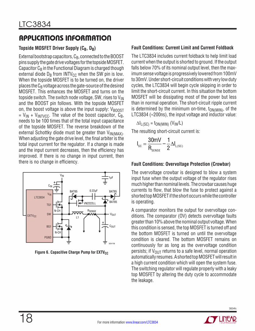
APPLICATIONS INFORMATIONTopside MOSFET Driver Supply (CB, DB)
External bootstrap capacitors, CB, connected to the BOOST pins supply the gate drive voltages for the topside MOSFET. Capacitor CB in the Functional Diagram is charged though external diode DB from INTVCC when the SW pin is low. When the topside MOSFET is to be turned on, the driver places the CB voltage across the gate-source of the desired MOSFET. This enhances the MOSFET and turns on the topside switch. The switch node voltage, SW, rises to VIN and the BOOST pin follows. With the topside MOSFET on, the boost voltage is above the input supply: VBOOST = VIN + VINTVCC. The value of the boost capacitor, CB, needs to be 100 times that of the total input capacitance of the topside MOSFET. The reverse breakdown of the external Schottky diode must be greater than VIN(MAX). When adjusting the gate drive level, the final arbiter is the total input current for the regulator. If a change is made and the input current decreases, then the efficiency has improved. If there is no change in input current, then there is no change in efficiency.
Fault Conditions: Current Limit and Current Foldback
The LTC3834 includes current foldback to help limit load current when the output is shorted to ground. If the output falls below 70% of its nominal output level, then the max-imum sense voltage is progressively lowered from 100mV to 30mV. Under short-circuit conditions with very low duty cycles, the LTC3834 will begin cycle skipping in order to limit the short-circuit current. In this situation the bottom MOSFET will be dissipating most of the power but less than in normal operation. The short-circuit ripple current is determined by the minimum on-time, tON(MIN), of the LTC3834 (≈200ns), the input voltage and inductor value:
∆IL(SC) = tON(MIN) (VIN/L)
The resulting short-circuit current is:
ISC =
30mVRSENSE
–12
∆IL(SC )
Fault Conditions: Overvoltage Protection (Crowbar)
The overvoltage crowbar is designed to blow a system input fuse when the output voltage of the regulator rises much higher than nominal levels. The crowbar causes huge currents to flow, that blow the fuse to protect against a shorted top MOSFET if the short occurs while the controller is operating.
A comparator monitors the output for overvoltage con-ditions. The comparator (OV) detects overvoltage faults greater than 10% above the nominal output voltage. When this condition is sensed, the top MOSFET is turned off and the bottom MOSFET is turned on until the overvoltage condition is cleared. The bottom MOSFET remains on continuously for as long as the overvoltage condition persists; if VOUT returns to a safe level, normal operation automatically resumes. A shorted top MOSFET will result in a high current condition which will open the system fuse. The switching regulator will regulate properly with a leaky top MOSFET by altering the duty cycle to accommodate the leakage.
EXTVCC
VIN
TG1
BG1
PGND
LTC3834
RSENSEVOUT
VN2222LL
+COUT
3834 F06
N-CH
N-CH
+CIN
1µF VIN
L1
BAT85 BAT85
BAT85
0.22µF
SW
Figure 6. Capacitive Charge Pump for EXTVCC

LTC3834
193834fc
For more information www.linear.com/LTC3834
APPLICATIONS INFORMATIONPhase-Locked Loop and Frequency Synchronization
The LTC3834 has a phase-locked loop (PLL) comprised of an internal voltage-controlled oscillator (VCO) and a phase detector. This allows the turn-on of the top MOSFET (TG) to be locked to the rising edge of an external clock signal applied to the PLLIN/MODE pin. The phase detector is an edge sensitive digital type that provides zero degrees phase shift between the external and internal oscillators. This type of phase detector does not exhibit false lock to harmonics of the external clock.
The output of the phase detector is a pair of complementary current sources that charge or discharge the external filter network connected to the PLLLPF pin. The relationship between the voltage on the PLLLPF pin and operating frequency, when there is a clock signal applied to PLLIN/MODE, is shown in Figure 7 and specified in the Electrical Characteristics table. Note that the LTC3834 can only be synchronized to an external clock whose frequency is within range of the LTC3834’s internal VCO, which is nominally 115kHz to 800kHz. This is guaranteed to be between 140kHz and 650kHz. A simplified block diagram is shown in Figure 8.
If the external clock frequency is greater than the internal oscillator’s frequency, fOSC, then current is sourced con-tinuously from the phase detector output, pulling up the PLLLPF pin. When the external clock frequency is less than fOSC, current is sunk continuously, pulling down the PLLLPF pin. If the external and internal frequencies are the same but exhibit a phase difference, the current sources turn on for an amount of time corresponding to the phase difference. The voltage on the PLLLPF pin is adjusted until the phase and frequency of the internal and external oscillators are identical. At the stable operating point, the phase detector output is high impedance and the filter capacitor CLP holds the voltage.
The loop filter components, CLP and RLP , smooth out the current pulses from the phase detector and provide a stable input to the voltage-controlled oscillator. The filter components CLP and RLP determine how fast the loop acquires lock. Typically RLP = 10k and CLP is 2200pF to 0.01µF.
Typically, the external clock (on PLLIN/MODE pin) input high threshold is 1.6V, while the input low threshold is 1.2V.
PLLLPF PIN VOLTAGE (V)0
FREQ
UENC
Y (k
Hz)
0.5 1 1.5 2
3835 F07
2.50
100
300
400
500
900
800
700
200
600
DIGITALPHASE/
FREQUENCYDETECTOR
OSCILLATOR
2.4V
RLP
CLP
3834 F08
PLLLPF
EXTERNALOSCILLATOR
PLLIN/MODE
Figure 7. Relationship Between Oscillator Frequency and Voltage at the PLLLPF Pin When Synchronizing to an External Clock
Figure 8. Phase-Locked Loop Block Diagram
LTC3834
203834fc
For more information www.linear.com/LTC3834
APPLICATIONS INFORMATIONTable 2 summarizes the different states in which the PLLLPF pin can be used.
Table 2PLLLPF PIN PLLIN/MODE PIN FREQUENCY
0V DC Voltage 250kHz
Floating DC Voltage 400kHz
INTVCC DC Voltage 530kHz
RC Loop Filter Clock Signal Phase-Locked to External Clock
Minimum On-Time Considerations
Minimum on-time, tON(MIN), is the smallest time duration that the LTC3834 is capable of turning on the top MOSFET. It is determined by internal timing delays and the gate charge required to turn on the top MOSFET. Low duty cycle applications may approach this minimum on-time limit and care should be taken to ensure that
tON(MIN) <
VOUT
VIN(f)
If the duty cycle falls below what can be accommodated by the minimum on-time, the controller will begin to skip cycles. The output voltage will continue to be regulated, but the ripple voltage and current will increase.
The minimum on-time for the LTC3834 is approximately 200ns. However, as the peak sense voltage decreases the minimum on-time gradually increases up to about 250ns. This is of particular concern in forced continuous applications with low ripple current at light loads. If the duty cycle drops below the minimum on-time limit in this situation, a significant amount of cycle skipping can occur with correspondingly larger current and voltage ripple.
Efficiency Considerations
The percent efficiency of a switching regulator is equal to the output power divided by the input power times 100%. It is often useful to analyze individual losses to determine what is limiting the efficiency and which change would produce the most improvement. Percent efficiency can be expressed as:
%Efficiency = 100% – (L1 + L2 + L3 + ...)
where L1, L2, etc. are the individual losses as a percentage of input power.
Although all dissipative elements in the circuit produce losses, four main sources usually account for most of the losses in LTC3834 circuits: 1) IC VIN current, 2) INT-VCC regulator current, 3) I2R losses, 4) Topside MOSFET transition losses.
1. The VIN current has two components: the first is the DC supply current given in the Electrical Characteris-tics table, which excludes MOSFET driver and control currents; the second is the current drawn from the 3.3V linear regulator output. VIN current typically results in a small (< 0.1%) loss.
2. INTVCC current is the sum of the MOSFET driver and control currents. The MOSFET driver current results from switching the gate capacitance of the power MOSFETs. Each time a MOSFET gate is switched from low to high to low again, a packet of charge dQ moves from INTVCC to ground. The resulting dQ/dt is a current out of INTVCC that is typically much larger than the control circuit current. In continuous mode, IGATECHG = f(QT + QB), where QT and QB are the gate charges of the topside and bottom side MOSFETs.
Supplying INTVCC power through the EXTVCC switch input from an output-derived source will scale the VIN current required for the driver and control circuits by a factor of (Duty Cycle)/(Efficiency). For example, in a 20V to 5V application, 10mA of INTVCC current results in approximately 2.5mA of VIN current. This reduces the mid-current loss from 10% or more (if the driver was powered directly from VIN) to only a few percent.
3. I2R losses are predicted from the DC resistances of the fuse (if used), MOSFET, inductor, current sense resis-tor, and input and output capacitor ESR. In continuous mode the average output current flows through L and RSENSE, but is “chopped” between the topside MOSFET and the synchronous MOSFET. If the two MOSFETs have approximately the same RDS(ON), then the resistance of one MOSFET can simply be summed with the resis-tances of L, RSENSE and ESR to obtain I2R losses. For example, if each RDS(ON) = 30mΩ, RL = 50mΩ, RSENSE = 10mΩ and RESR = 40mΩ (sum of both input and output capacitance losses), then the total resistance is 130mΩ. This results in losses ranging from 3% to 13% as the output current increases from 1A to 5A for
LTC3834
213834fc
For more information www.linear.com/LTC3834
APPLICATIONS INFORMATIONa 5V output, or a 4% to 20% loss for a 3.3V output. Efficiency varies as the inverse square of VOUT for the same external components and output power level. The combined effects of increasingly lower output voltages and higher currents required by high performance digital systems is not doubling but quadrupling the importance of loss terms in the switching regulator system!
4. Transition losses apply only to the topside MOSFET, and become significant only when operating at high input voltages (typically 15V or greater). Transition losses can be estimated from:
Transition Loss = (1.7) VIN2 IO(MAX) CRSS f
Other “hidden” losses such as copper trace and internal battery resistances can account for an additional 5% to 10% efficiency degradation in portable systems. It is very important to include these “system” level losses during the design phase. The internal battery and fuse resistance losses can be minimized by making sure that CIN has ad-equate charge storage and very low ESR at the switching frequency. A 25W supply will typically require a minimum of 20µF to 40µF of capacitance having a maximum of 20mΩ to 50mΩ of ESR. Other losses including Schottky con-duction losses during dead-time and inductor core losses generally account for less than 2% total additional loss.
Checking Transient Response
The regulator loop response can be checked by looking at the load current transient response. Switching regulators take several cycles to respond to a step in DC (resistive) load current. When a load step occurs, VOUT shifts by an amount equal to ∆ILOAD (ESR), where ESR is the effective series resistance of COUT . ∆ILOAD also begins to charge or discharge COUT generating the feedback error signal that forces the regulator to adapt to the current change and return VOUT to its steady-state value. During this recov-ery time VOUT can be monitored for excessive overshoot or ringing, which would indicate a stability problem. OPTI-LOOP compensation allows the transient response to be optimized over a wide range of output capacitance and ESR values. The availability of the ITH pin not only allows optimization of control loop behavior but also pro-vides a DC coupled and AC filtered closed-loop response
test point. The DC step, rise time and settling at this test point truly reflects the closed-loop response. Assuming a predominantly second order system, phase margin and/or damping factor can be estimated using the percentage of overshoot seen at this pin. The bandwidth can also be estimated by examining the rise time at the pin. The ITH external components shown in the Typical Application circuit will provide an adequate starting point for most applications.
The ITH series RC-CC filter sets the dominant pole-zero loop compensation. The values can be modified slightly (from 0.5 to 2 times their suggested values) to optimize transient response once the final PC layout is done and the particular output capacitor type and value have been determined. The output capacitors need to be selected because the various types and values determine the loop gain and phase. An output current pulse of 20% to 80% of full-load current having a rise time of 1µs to 10µs will produce output voltage and ITH pin waveforms that will give a sense of the overall loop stability without breaking the feedback loop. Placing a power MOSFET directly across the output capacitor and driving the gate with an appropriate signal generator is a practical way to produce a realistic load step condition. The initial output voltage step resulting from the step change in output current may not be within the bandwidth of the feedback loop, so this signal cannot be used to determine phase margin. This is why it is better to look at the ITH pin signal which is in the feedback loop and is the filtered and compensated control loop response. The gain of the loop will be in-creased by increasing RC and the bandwidth of the loop will be increased by decreasing CC. If RC is increased by the same factor that CC is decreased, the zero frequency will be kept the same, thereby keeping the phase shift the same in the most critical frequency range of the feedback loop. The output voltage settling behavior is related to the stability of the closed-loop system and will demonstrate the actual overall supply performance.
A second, more severe transient is caused by switching in loads with large (>1µF) supply bypass capacitors. The discharged bypass capacitors are effectively put in parallel with COUT , causing a rapid drop in VOUT . No regulator can alter its delivery of current quickly enough to prevent this
LTC3834
223834fc
For more information www.linear.com/LTC3834
APPLICATIONS INFORMATIONsudden step change in output voltage if the load switch resistance is low and it is driven quickly. If the ratio of CLOAD to COUT is greater than 1:50, the switch rise time should be controlled so that the load rise time is limited to approximately 25 • CLOAD. Thus a 10µF capacitor would require a 250µs rise time, limiting the charging current to about 200mA.
Design Example
As a design example, assume VIN = 12V(nominal), VIN = 22V(max), VOUT = 1.8V, IMAX = 5A, and f = 250kHz.
The inductance value is chosen first based on a 30% ripple current assumption. The highest value of ripple current occurs at the maximum input voltage. Tie the PLLLPF pin to GND, generating 250kHz operation. The minimum inductance for 30% ripple current is:
∆IL =
VOUT
(f)(L)1–
VOUT
VIN
A 4.7µH inductor will produce 23% ripple current and a 3.3µH will result in 33%. The peak inductor current will be the maximum DC value plus one half the ripple current, or 5.84A, for the 3.3µH value. Increasing the ripple current will also help ensure that the minimum on-time of 180ns is not violated. The minimum on-time occurs at maximum VIN:
tON(MIN) =
VOUT
VIN(MAX )f=
1.8V22V(250kHz)
= 327ns
The RSENSE resistor value can be calculated by using the maximum current sense voltage specification with some accommodation for tolerances:
RSENSE ≤
80mV5.84A
≈ 0.012Ω
Choosing 1% resistors: R1 = 25.5k and R2 = 32.4k yields an output voltage of 1.816V.
The power dissipation on the topside MOSFET can be easily estimated. Choosing a Fairchild FDS6982S dual MOSFET results in: RDS(ON) = 0.035Ω/0.022Ω, CMILLER = 215pF. At maximum input voltage with T(estimated) = 50°C:
PMAIN =1.8V22V
5( )2 1+ (0.005)(50°C – 25°C)[ ] •
0.035Ω( ) + 22V( )2 5A2
4Ω( ) 215pF( ) •
15 – 2.3
+1
2.3
300kHz( ) = 332mW
A short-circuit to ground will result in a folded back cur-rent of:
ISC =
25mV0.01Ω
–12
120ns(22V)3.3µH
= 2.1A
with a typical value of RDS(ON) and δ = (0.005/°C)(20) = 0.1. The resulting power dissipated in the bottom MOSFET is:
PSYNC =22V – 1.8V
22V2.1A( )2 1.125( ) 0.022Ω( )
= 100mW
which is less than under full-load conditions.
CIN is chosen for an RMS current rating of at least 3A at temperature assuming only this channel is on. COUT is chosen with an ESR of 0.02Ω for low output ripple. The output ripple in continuous mode will be highest at the maximum input voltage. The output voltage ripple due to ESR is approximately:
VORIPPLE = RESR (∆IL) = 0.02Ω(1.67A) = 33mVP-P
LTC3834
233834fc
For more information www.linear.com/LTC3834
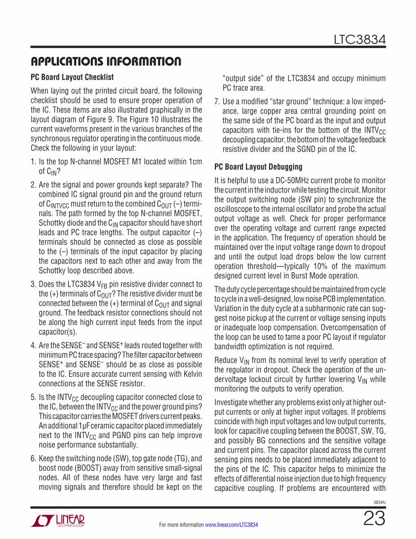
APPLICATIONS INFORMATIONPC Board Layout Checklist
When laying out the printed circuit board, the following checklist should be used to ensure proper operation of the IC. These items are also illustrated graphically in the layout diagram of Figure 9. The Figure 10 illustrates the current waveforms present in the various branches of the synchronous regulator operating in the continuous mode. Check the following in your layout:
1. Is the top N-channel MOSFET M1 located within 1cm of CIN?
2. Are the signal and power grounds kept separate? The combined IC signal ground pin and the ground return of CINTVCC must return to the combined COUT (–) termi-nals. The path formed by the top N-channel MOSFET, Schottky diode and the CIN capacitor should have short leads and PC trace lengths. The output capacitor (–) terminals should be connected as close as possible to the (–) terminals of the input capacitor by placing the capacitors next to each other and away from the Schottky loop described above.
3. Does the LTC3834 VFB pin resistive divider connect to the (+) terminals of COUT? The resistive divider must be connected between the (+) terminal of COUT and signal ground. The feedback resistor connections should not be along the high current input feeds from the input capacitor(s).
4. Are the SENSE– and SENSE+ leads routed together with minimum PC trace spacing? The filter capacitor between SENSE+ and SENSE– should be as close as possible to the IC. Ensure accurate current sensing with Kelvin connections at the SENSE resistor.
5. Is the INTVCC decoupling capacitor connected close to the IC, between the INTVCC and the power ground pins? This capacitor carries the MOSFET drivers current peaks. An additional 1µF ceramic capacitor placed immediately next to the INTVCC and PGND pins can help improve noise performance substantially.
6. Keep the switching node (SW), top gate node (TG), and boost node (BOOST) away from sensitive small-signal nodes. All of these nodes have very large and fast moving signals and therefore should be kept on the
“output side” of the LTC3834 and occupy minimum PC trace area.
7. Use a modified “star ground” technique: a low imped-ance, large copper area central grounding point on the same side of the PC board as the input and output capacitors with tie-ins for the bottom of the INTVCC decoupling capacitor, the bottom of the voltage feedback resistive divider and the SGND pin of the IC.
PC Board Layout Debugging
It is helpful to use a DC-50MHz current probe to monitor the current in the inductor while testing the circuit. Monitor the output switching node (SW pin) to synchronize the oscilloscope to the internal oscillator and probe the actual output voltage as well. Check for proper performance over the operating voltage and current range expected in the application. The frequency of operation should be maintained over the input voltage range down to dropout and until the output load drops below the low current operation threshold—typically 10% of the maximum designed current level in Burst Mode operation.
The duty cycle percentage should be maintained from cycle to cycle in a well-designed, low noise PCB implementation. Variation in the duty cycle at a subharmonic rate can sug-gest noise pickup at the current or voltage sensing inputs or inadequate loop compensation. Overcompensation of the loop can be used to tame a poor PC layout if regulator bandwidth optimization is not required.
Reduce VIN from its nominal level to verify operation of the regulator in dropout. Check the operation of the un-dervoltage lockout circuit by further lowering VIN while monitoring the outputs to verify operation.
Investigate whether any problems exist only at higher out-put currents or only at higher input voltages. If problems coincide with high input voltages and low output currents, look for capacitive coupling between the BOOST, SW, TG, and possibly BG connections and the sensitive voltage and current pins. The capacitor placed across the current sensing pins needs to be placed immediately adjacent to the pins of the IC. This capacitor helps to minimize the effects of differential noise injection due to high frequency capacitive coupling. If problems are encountered with

LTC3834
243834fc
For more information www.linear.com/LTC3834
APPLICATIONS INFORMATIONhigh current output loading at lower input voltages, look for inductive coupling between CIN, Schottky and the top MOSFET components to the sensitive current and voltage sensing traces. In addition, investigate common ground path voltage pickup between these components and the SGND pin of the IC.
An embarrassing problem, which can be missed in an otherwise properly working switching regulator, results
when the current sensing leads are hooked up backwards. The output voltage under this improper hookup will still be maintained but the advantages of current mode control will not be realized. Compensation of the voltage loop will be much more sensitive to component selection. This behavior can be investigated by temporarily shorting out the current sensing resistor—don’t worry, the regulator will still maintain control of the output voltage.
C11nF
CB
DB
M2
M1
CIN
L1
COUT
VOUT
VIN
3834 F09
CLKO
UT
PLLL
PF
I TH
TRAC
K/SS
V FB
SGND
PGND
BG INTV
CC
EXTV
CC
PHAS
MD
PLLI
N/M
ODE
PGOO
D
SENS
E+
SENS
E–
RUN
BOOS
T TG SW V IN
LTC3
834E
FE
D1OPTIONAL
RL1D1
L1SW RSENSE VOUT
COUT
VIN
CIN
RIN
BOLD LINES INDICATE HIGH SWITCHING CURRENT. KEEP LINES TO A MINIMUM LENGTH.
3834 F10
Figure 9. LTC3834 Recommended Printed Circuit Layout Diagram
Figure 10. Branch Current Waveforms
LTC3834
253834fc
For more information www.linear.com/LTC3834
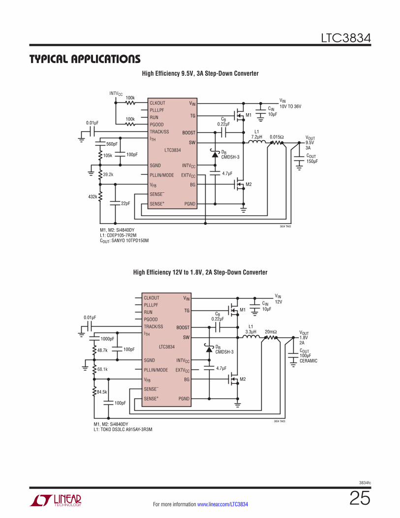
TYPICAL APPLICATIONS
COUT150µF
VOUT9.5V3A
0.01µF
VIN10V TO 36V
M1
M2
ITH
SGND
PLLIN/MODE
VFB
SENSE+
SENSE–
CLKOUT
PLLLPF
RUN
PGOOD
TRACK/SS
INTVCC
EXTVCC
BG
PGND
LTC3834
L17.2µH 0.015Ω
39.2k
3834 TA02
100pF
560pF
105k
432k
100k
100k
4.7µF
DBCMDSH-3
CB0.22µF
TG
VIN
BOOST
SW
CIN10µF
22pF
INTVCC
M1, M2: Si4840DYL1: CDEP105-7R2MCOUT: SANYO 10TPD150M
High Efficiency 9.5V, 3A Step-Down Converter
High Efficiency 12V to 1.8V, 2A Step-Down Converter
COUT100µFCERAMIC
VOUT1.8V2A
0.01µF
VIN12V
M1
M2
ITH
SGND
PLLIN/MODE
VFB
SENSE+
SENSE–
CLKOUT
PLLLPF
RUN
PGOOD
TRACK/SS
INTVCC
EXTVCC
BG
PGND
LTC3834
L13.3µH 20mΩ
68.1k
3834 TA03
100pF
1000pF
48.7k
84.5k
4.7µF
DBCMDSH-3
CB0.22µF
TG
VIN
BOOST
SW
CIN10µF
100pF
M1, M2: Si4840DYL1: TOKO DS3LC A915AY-3R3M
LTC3834
263834fc
For more information www.linear.com/LTC3834
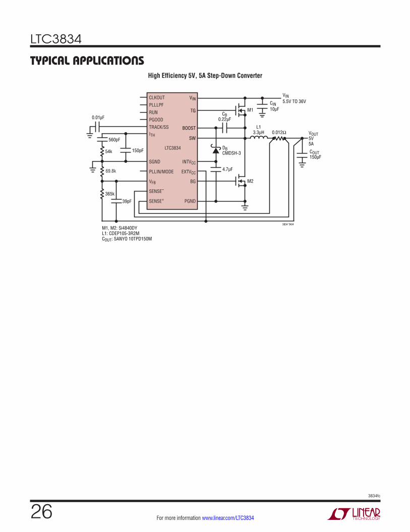
TYPICAL APPLICATIONSHigh Efficiency 5V, 5A Step-Down Converter
COUT150µF
VOUT5V5A
0.01µF
VIN5.5V TO 36V
M1
M2
ITH
SGND
PLLIN/MODE
VFB
SENSE+
SENSE–
CLKOUT
PLLLPF
RUN
PGOOD
TRACK/SS
INTVCC
EXTVCC
BG
PGND
LTC3834
L13.3µH 0.012Ω
69.8k
3834 TA04
150pF
560pF
54k
365k
4.7µF
DBCMDSH-3
CB0.22µF
TG
VIN
BOOST
SW
CIN10µF
39pF
M1, M2: Si4840DYL1: CDEP105-3R2MCOUT: SANYO 10TPD150M
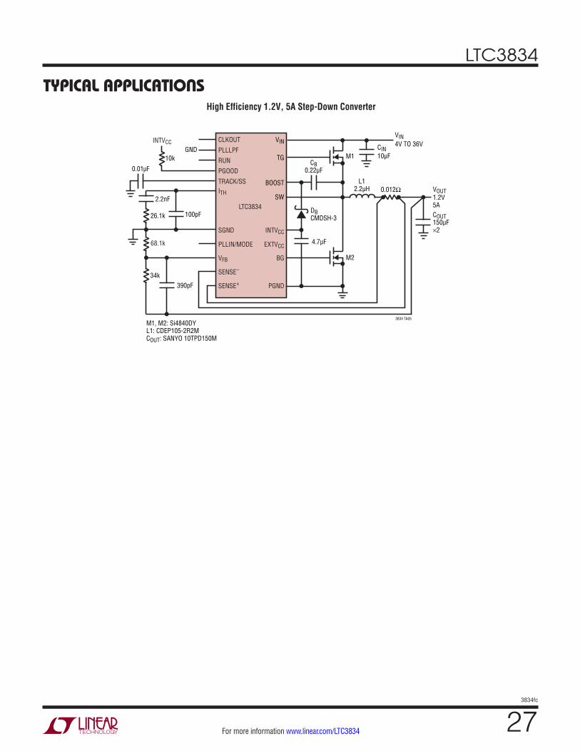
LTC3834
273834fc
For more information www.linear.com/LTC3834
High Efficiency 1.2V, 5A Step-Down Converter
VOUT1.2V5ACOUT150µF ×2
0.01µF
VIN4V TO 36V
M1
M2
ITH
SGND
PLLIN/MODE
VFB
SENSE+
SENSE–
CLKOUT
PLLLPF
RUN
PGOOD
TRACK/SS
INTVCC
EXTVCC
BG
PGND
LTC3834
L12.2µH 0.012Ω
10k
68.1k
3834 TA05
100pF
GND
2.2nF
26.1k
34k
4.7µF
DBCMDSH-3
CB0.22µF
TG
VIN
BOOST
SW
CIN10µF
INTVCC
390pF
M1, M2: Si4840DYL1: CDEP105-2R2MCOUT: SANYO 10TPD150M
TYPICAL APPLICATIONS
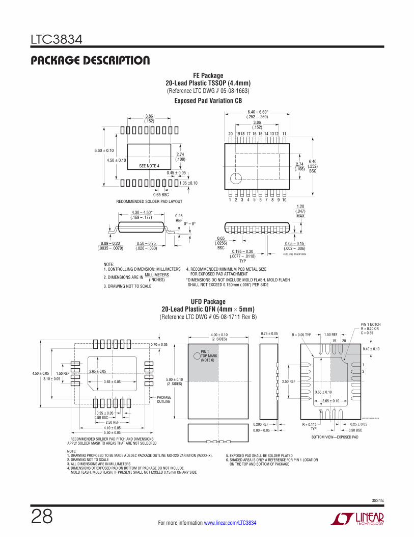
LTC3834
283834fc
For more information www.linear.com/LTC3834
PACKAGE DESCRIPTIONFE Package
20-Lead Plastic TSSOP (4.4mm)(Reference LTC DWG # 05-08-1663)
Exposed Pad Variation CB
UFD Package20-Lead Plastic QFN (4mm × 5mm)
(Reference LTC DWG # 05-08-1711 Rev B)
FE20 (CB) TSSOP 0204
0.09 – 0.20(.0035 – .0079)
0° – 8°
0.25REF
RECOMMENDED SOLDER PAD LAYOUT
0.50 – 0.75(.020 – .030)
4.30 – 4.50*(.169 – .177)
1 3 4 5 6 7 8 9 10
111214 13
6.40 – 6.60*(.252 – .260)
3.86(.152)
2.74(.108)
20 1918 17 16 15
1.20(.047)MAX
0.05 – 0.15(.002 – .006)
0.65(.0256)
BSC0.195 – 0.30
(.0077 – .0118)TYP
2
2.74(.108)
0.45 ± 0.05
0.65 BSC
4.50 ± 0.10
6.60 ± 0.10
1.05 ±0.10
3.86(.152)
MILLIMETERS(INCHES) *DIMENSIONS DO NOT INCLUDE MOLD FLASH. MOLD FLASH
SHALL NOT EXCEED 0.150mm (.006") PER SIDE
NOTE:1. CONTROLLING DIMENSION: MILLIMETERS
2. DIMENSIONS ARE IN
3. DRAWING NOT TO SCALE
SEE NOTE 4
4. RECOMMENDED MINIMUM PCB METAL SIZE FOR EXPOSED PAD ATTACHMENT
6.40(.252)BSC
4.00 ± 0.10(2 SIDES)
1.50 REF
5.00 ± 0.10(2 SIDES)
NOTE:1. DRAWING PROPOSED TO BE MADE A JEDEC PACKAGE OUTLINE MO-220 VARIATION (WXXX-X).2. DRAWING NOT TO SCALE3. ALL DIMENSIONS ARE IN MILLIMETERS4. DIMENSIONS OF EXPOSED PAD ON BOTTOM OF PACKAGE DO NOT INCLUDE MOLD FLASH. MOLD FLASH, IF PRESENT, SHALL NOT EXCEED 0.15mm ON ANY SIDE
5. EXPOSED PAD SHALL BE SOLDER PLATED6. SHADED AREA IS ONLY A REFERENCE FOR PIN 1 LOCATION ON THE TOP AND BOTTOM OF PACKAGE
PIN 1TOP MARK(NOTE 6)
0.40 ± 0.10
19 20
1
2
BOTTOM VIEW—EXPOSED PAD
2.50 REF
0.75 ± 0.05
R = 0.115TYP
PIN 1 NOTCHR = 0.20 ORC = 0.35
0.25 ± 0.05
0.50 BSC
0.200 REF
0.00 – 0.05
(UFD20) QFN 0506 REV B
R = 0.05 TYP
2.65 ± 0.10
3.65 ± 0.10
RECOMMENDED SOLDER PAD PITCH AND DIMENSIONSAPPLY SOLDER MASK TO AREAS THAT ARE NOT SOLDERED
0.70 ± 0.05
0.25 ± 0.05
2.65 ± 0.05
2.50 REF4.10 ± 0.055.50 ± 0.05
1.50 REF3.10 ± 0.05
4.50 ± 0.05
PACKAGE OUTLINE
3.65 ± 0.05
0.50 BSC
LTC3834
293834fc
For more information www.linear.com/LTC3834
Information furnished by Linear Technology Corporation is believed to be accurate and reliable. However, no responsibility is assumed for its use. Linear Technology Corporation makes no representation that the interconnection of its circuits as described herein will not infringe on existing patent rights.
REVISION HISTORYREV DATE DESCRIPTION PAGE NUMBER
C 02/15 Changed VIN to INTVCC in PLLPF pin function description. 8
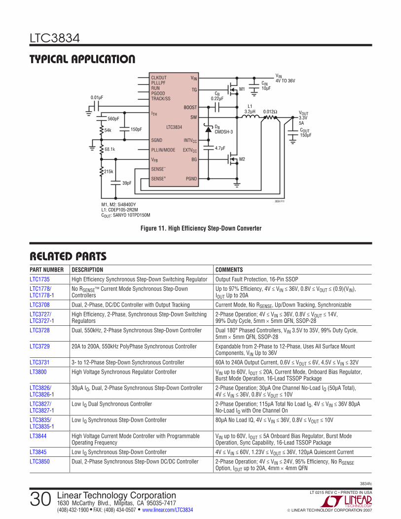
LTC3834
303834fc
LINEAR TECHNOLOGY CORPORATION 2007
LT 0215 REV C • PRINTED IN USA
For more information www.linear.com/LTC3834
RELATED PARTS
TYPICAL APPLICATION
VOUT3.3V5ACOUT150µF
0.01µF
VIN4V TO 36V
M1
M2
ITH
SGND
PLLIN/MODE
VFB
SENSE+
SENSE–
CLKOUTPLLLPFRUNPGOODTRACK/SS
INTVCC
EXTVCC
BG
PGND
LTC3834
L13.2µH 0.012Ω
68.1k
3834 F11
150pF
560pF
54k
215k
M1, M2: Si4840DYL1: CDEP105-2R2MCOUT: SANYO 10TPD150M
4.7µF
DBCMDSH-3
CB0.22µF
TG
VIN
BOOST
SW
CIN10µF
39pF
Figure 11. High Efficiency Step-Down Converter
PART NUMBER DESCRIPTION COMMENTS
LTC1735 High Efficiency Synchronous Step-Down Switching Regulator Output Fault Protection, 16-Pin SSOP
LTC1778/ LTC1778-1
No RSENSE Current Mode Synchronous Step-Down Controllers
Up to 97% Efficiency, 4V ≤ VIN ≤ 36V, 0.8V ≤ VOUT ≤ (0.9)(VIN), IOUT Up to 20A
LTC3708 Dual, 2-Phase, DC/DC Controller with Output Tracking Current Mode, No RSENSE, Up/Down Tracking, Synchronizable
LTC3727/ LTC3727-1
High Efficiency, 2-Phase, Synchronous Step-Down Switching Regulators
2-Phase Operation; 4V ≤ VIN ≤ 36V, 0.8V ≤ VOUT ≤ 14V, 99% Duty Cycle, 5mm × 5mm QFN, SSOP-28
LTC3728 Dual, 550kHz, 2-Phase Synchronous Step-Down Controller Dual 180° Phased Controllers, VIN 3.5V to 35V, 99% Duty Cycle, 5mm × 5mm QFN, SSOP-28
LTC3729 20A to 200A, 550kHz PolyPhase Synchronous Controller Expandable from 2-Phase to 12-Phase, Uses All Surface Mount Components, VIN Up to 36V
LTC3731 3- to 12-Phase Step-Down Synchronous Controller 60A to 240A Output Current, 0.6V ≤ VOUT ≤ 6V, 4.5V ≤ VIN ≤ 32V
LT3800 High Voltage Synchronous Regulator Controller VIN up to 60V, IOUT ≤ 20A, Current Mode, Onboard Bias Regulator, Burst Mode Operation, 16-Lead TSSOP Package
LTC3826/ LTC3826-1
30µA IQ, Dual, 2-Phase Synchronous Step-Down Controller 2-Phase Operation; 30µA One Channel No-Load IQ (50µA Total), 4V ≤ VIN ≤ 36V, 0.8V ≤ VOUT ≤ 10V
LTC3827/ LTC3827-1
Low IQ Dual Synchronous Controller 2-Phase Operation; 115µA Total No Load IQ, 4V ≤ VIN ≤ 36V 80µA No-Load IQ with One Channel On
LTC3835/ LTC3835-1
Low IQ Synchronous Step-Down Controller 80µA No Load IQ, 4V ≤ VIN ≤ 36V, 0.8V ≤ VOUT ≤ 10V
LT3844 High Voltage Current Mode Controller with Programmable Operating Frequency
VIN up to 60V, IOUT ≤ 5A Onboard Bias Regulator, Burst Mode Operation, Sync Capability, 16-Lead TSSOP Package
LT3845 Low IQ Synchronous Step-Down Controller 4V ≤ VIN ≤ 60V, 1.23V ≤ VOUT ≤ 36V, 120µA Quiescent Current
LTC3850 Dual, 2-Phase Synchronous Step-Down DC/DC Controller 2-Phase Operation; 4V ≤ VIN ≤ 24V, 95% Efficiency, No RSENSE Option, IOUT up to 20A, 4mm × 4mm QFN
Linear Technology Corporation1630 McCarthy Blvd., Milpitas, CA 95035-7417(408) 432-1900 FAX: (408) 434-0507 www.linear.com/LTC3834