high efficiency monolithic synchronous step-down … · high efficiency monolithic synchronous...
TRANSCRIPT

October 2016 DocID11051 Rev 9 1/21
This is information on a product in full production. www.st.com
L6928
High efficiency monolithic synchronous step-down regulator
Datasheet - production data
Features 2 V to 5.5 V battery input range
High efficiency: up to 95%
Internal synchronous switch
No external Schottky diode required
Extremely low quiescent current
1 µA max. shutdown supply current
800 mA max. output current
Adjustable output voltage from 0.6 V
Low-dropout operation: up to 100% duty cycle
Selectable low noise/low consumption mode at light load
Power Good signal
± 1% output voltage accuracy
Current mode control
1.4 MHz switching frequency
Externally synchronized from 1 MHz to 2 MHz
OVP
Short-circuit protection
Applications Battery-powered equipment
Portable instruments
Cellular phones
PDAs and handheld terminals
DSC
GPS
Description The device is a DC-DC monolithic regulator specifically designed to provide high efficiency. The L6928 supply voltage can be as low as 2 V to be used in single Li-Ion cell supplied applications. Output voltage can be selected by an external divider down to 0.6 V. Duty cycle can saturate 100% allowing low-dropout operation. The device is based on a 1.4 MHz fixed frequency, current mode architecture. Low consumption mode operation can be selected at light load conditions, allowing switching losses to be reduced. The L6928 is externally synchronized by a clock, which makes it useful in noise sensitive applications. Other features like Power Good, overvoltage protection, short-circuit protection and thermal shutdown (150 °C) are also present.
Table 1: Device summary
Order code Package Packing
L6928D TSSOP8 Tube
L6928D013TR TSSOP8 Tape and reel
L6928Q1 VFQFPN8 Tube
L6928Q1TR VFQFPN8 Tape and reel
VFQFPN8TSSOP8
(3x3x1.0 mm)

Contents L6928
2/21 DocID11051 Rev 9
Contents
1 Application circuit ........................................................................... 5
2 Pin configuration ............................................................................. 6
3 Maximum ratings ............................................................................. 7
4 Electrical characteristics ................................................................ 8
5 Detailed description ...................................................................... 10
5.1 Modes of operation ......................................................................... 10
5.1.1 Low consumption mode.................................................................... 10
5.1.2 Low noise mode ............................................................................... 11
5.1.3 Synchronization ................................................................................ 11
5.2 Short-circuit protection .................................................................... 11
5.3 Slope compensation ........................................................................ 12
5.4 Loop stability ................................................................................... 12
6 Additional features and description ............................................. 13
6.1 Dropout operation ........................................................................... 13
6.2 PGOOD ........................................................................................... 13
6.3 Adjustable output voltage ................................................................ 13
6.4 OVP (overvoltage protection) .......................................................... 13
6.5 Thermal shutdown ........................................................................... 13
7 Package information ..................................................................... 14
7.1 TSSOP8 package information ......................................................... 15
7.2 VFQFPN8 package information ...................................................... 17
8 Revision history ............................................................................ 20

L6928 List of tables
DocID11051 Rev 9 3/21
List of tables
Table 1: Device summary ........................................................................................................................... 1 Table 2: Pin description .............................................................................................................................. 6 Table 3: Absolute maximum ratings ........................................................................................................... 7 Table 4: Thermal data ................................................................................................................................. 7 Table 5: Electrical characteristics ............................................................................................................... 8 Table 6: TSSOP8 package mechanical data ............................................................................................ 16 Table 7: VFQFPN8 package mechanical data ......................................................................................... 18 Table 8: Document revision history .......................................................................................................... 20

List of figures L6928
4/21 DocID11051 Rev 9
List of figures
Figure 1: L6928 application circuit .............................................................................................................. 5 Figure 2: Pin connections (top view) ........................................................................................................... 6 Figure 3: Device block diagram ................................................................................................................ 10 Figure 4: TSSOP8 package outline .......................................................................................................... 15 Figure 5: VFQFPN8 package outline ........................................................................................................ 17 Figure 6: VFQFPN8 recommended footprint ............................................................................................ 19
L6928 Application circuit
DocID11051 Rev 9 5/21
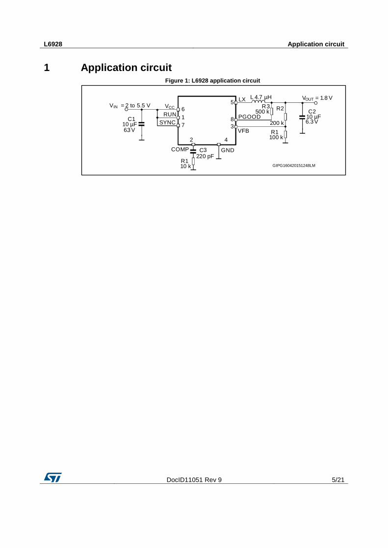
1 Application circuit Figure 1: L6928 application circuit
VIN = 2 to 5.5 V
VOUT = 1.8 V
C110 µF6.3 V R1
100 k
R 3500 k
R2
200 k
L 4.7 µH
C210 µF6.3 V
C220 pF
R110 k
LX
PGOOD
VFB
GNDCOMP
VCC
RUN
SYNC
5
8
37
1
6
2 4
3
GIPG160420151248LM

Pin configuration L6928
6/21 DocID11051 Rev 9
2 Pin configuration Figure 2: Pin connections (top view)
Table 2: Pin description
Pin Name Description
1 RUN
Shutdown input. When connected to a low level (lower than
0.4 V) the device stops working. When high (higher than 1.3
V) the device is enabled
2 COMP
Error amplifier output. A compensation network has to be
connected to this pin. The loop stability usually is well-
guaranteed by a 220 pF capacitor
3 VFB
Error amplifier inverting input. The output voltage can be
adjusted from 0.6 V up to the input voltage by connecting
this pin to an external resistor divider
4 GND Ground
5 LX Switch output node. This pin is internally connected to the
drain of the internal switches
6 VCC
Input voltage. The start-up input voltage is 2.2 V (typ.) while the operating input voltage range is from 2 V to 5.5 V. An internal UVLO circuit realizes a 100 mV (typ.) hysteresis
7 SYNC
Operating mode selector input. When high (higher than 1.3 V) the low consumption mode is selected. When low (lower than 0.5 V) the low noise mode is selected. If connected with an appropriate external synchronization signal (from 1 MHz up to 2 MHz) the internal synchronization circuit is active and the device works at the same switching frequency
8 PGOOD
Power Good comparator output. It is an open drain output. A pull-up resistor should be connected between PGOOD and VOUT (or VCC depending on the requirements). The pin is forced low when the output voltage is lower than 90% of the regulated output voltage and goes high when the output voltage is greater than 90% of the regulated output voltage. If it is not used the pin can be left floating
- E-pad To be connected to GND plane for optimal thermal performance
RUN
COMP
VFB
GND
1
3
2
4 LX
VCC
SYNC
PGOOD8
7
6
5
D01IN1239AMOD
1
2
3
4
8
7
6
5
RUN
COMP
VFB
GND
PGOOD
SYNC
VCC
LX
E-pad
GIPG100420151039LM

L6928 Maximum ratings
DocID11051 Rev 9 7/21
3 Maximum ratings Table 3: Absolute maximum ratings
Symbol Parameter Value Unit
V6 Input voltage - 0.3 to + 6.0 V
V5 Output switching voltage - 1 to VCC V
V1 Shutdown -0.3 to VCC V
V3 Feedback voltage -0.3 to VCC V
V2 Error amplifier output voltage -0.3 to VCC V
V8 PGOOD -0.3 to VCC V
V7 Synchronization mode selector -0.3 to VCC V
PTOT Power dissipation at TA = 70 °C 0.45 W
TJ Junction operating temperature
range -40 to 150 °C
TSTG Storage temperature range -65 to 150
LX pin Maximum withstanding voltage
range test condition: CDF-AEC-
Q100-002 “human body model”
acceptance criteria: “normal
performance"
±1000
V Other pins ±2000
Table 4: Thermal data
Symbol Parameter Value Unit
RthJA
Thermal resistance junction-ambient
for TSSOP8 180
°C/W Thermal resistance junction-ambient
for VFQFPN8 56
Electrical characteristics L6928
8/21 DocID11051 Rev 9
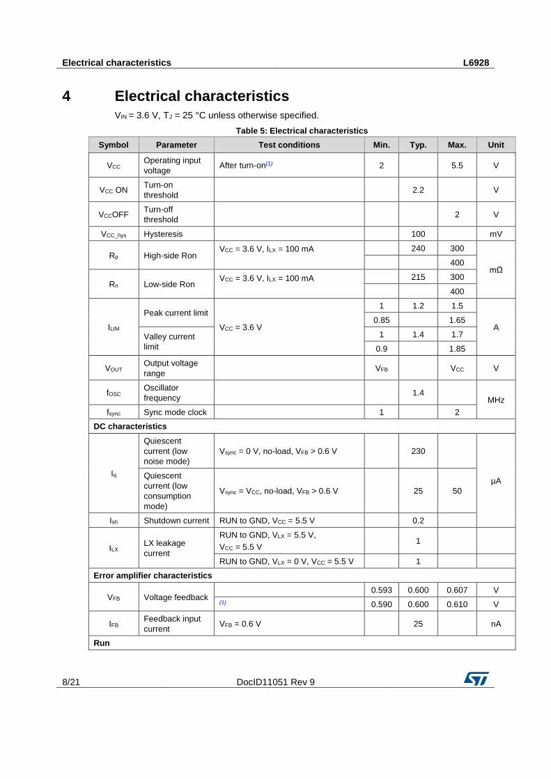
4 Electrical characteristics
VIN = 3.6 V, TJ = 25 °C unless otherwise specified.
Table 5: Electrical characteristics
Symbol Parameter Test conditions Min. Typ. Max. Unit
VCC Operating input
voltage After turn-on(1) 2
5.5 V
VCC ON Turn-on
threshold 2.2
V
VCCOFF Turn-off
threshold 2 V
VCC_hys Hysteresis
100
mV
Rp High-side Ron VCC = 3.6 V, ILX = 100 mA
240 300
mΩ 400
Rn Low-side Ron VCC = 3.6 V, ILX = 100 mA
215 300
400
ILIM
Peak current limit
VCC = 3.6 V
1 1.2 1.5
A 0.85
1.65
Valley current
limit
1 1.4 1.7
0.9
1.85
VOUT Output voltage
range VFB
VCC V
fOSC Oscillator
frequency 1.4
MHz
fsync Sync mode clock
1
2
DC characteristics
Iq
Quiescent
current (low
noise mode)
Vsync = 0 V, no-load, VFB > 0.6 V
230
µA Quiescent
current (low
consumption
mode)
Vsync = VCC, no-load, VFB > 0.6 V
25 50
Ish Shutdown current RUN to GND, VCC = 5.5 V
0.2
ILX LX leakage
current
RUN to GND, VLX = 5.5 V,
VCC = 5.5 V 1
RUN to GND, VLX = 0 V, VCC = 5.5 V
1
Error amplifier characteristics
VFB Voltage feedback 0.593 0.600 0.607 V
(1) 0.590 0.600 0.610 V
IFB Feedback input
current VFB = 0.6 V
25
nA
Run

L6928 Electrical characteristics
DocID11051 Rev 9 9/21
Symbol Parameter Test conditions Min. Typ. Max. Unit
VRUN_H Run threshold
high 1.3 V
VRUN_L Run threshold
low 0.4
V
IRUN RUN input
current 25
nA
SYNC/MODE function
Vsync_H Sync mode
threshold high 1.3 V
Vsync_L Sync mode
threshold low 0.5
V
Power Good section
VPGOOD Power Good
threshold VOUT = VFB
90
%VOUT
ΔVPGOOG Power Good
hysteresis VOUT = VFB
4
VPGOOD(low) Power Good low
voltage RUN to GND
0.4 V
ILK-PGOOD Power Good
leakage current VPGOOD = 3.6 V
50
nA
Protections
HOVP Hard overvoltage
threshold VOUT = VFB
10
%VOUT
Notes:
(1)Specification referred to TJ from -40 °C to +125 °C. Specification over the -40 to +125 °C TJ temperature range is assured by design, characterization and statistical correlation.
Detailed description L6928
10/21 DocID11051 Rev 9
VCCSYNC
P
DRIVER
Vcc
LOOPCONTROL
OSCILLATOR
LOWNOISE/
CONSUMPTION
LX
OVP
VFB
PGOODVREF
0.9 V
RUN
COM P
GOOD
GN D
DRIVER
GND
GND
GNDPEAK
CL
VALLEYCL
Zero-crossing
LOOPCONTROL
OSCILLATOR
LOWNOISE/
CONSUMPTION
OVP
VREF
E/A
POWERPMOS
POWERNMOS
SENSE
PMOS
SENSENMOS
Vcc
0.6 V
SLOPE
GIPG140420151256LM
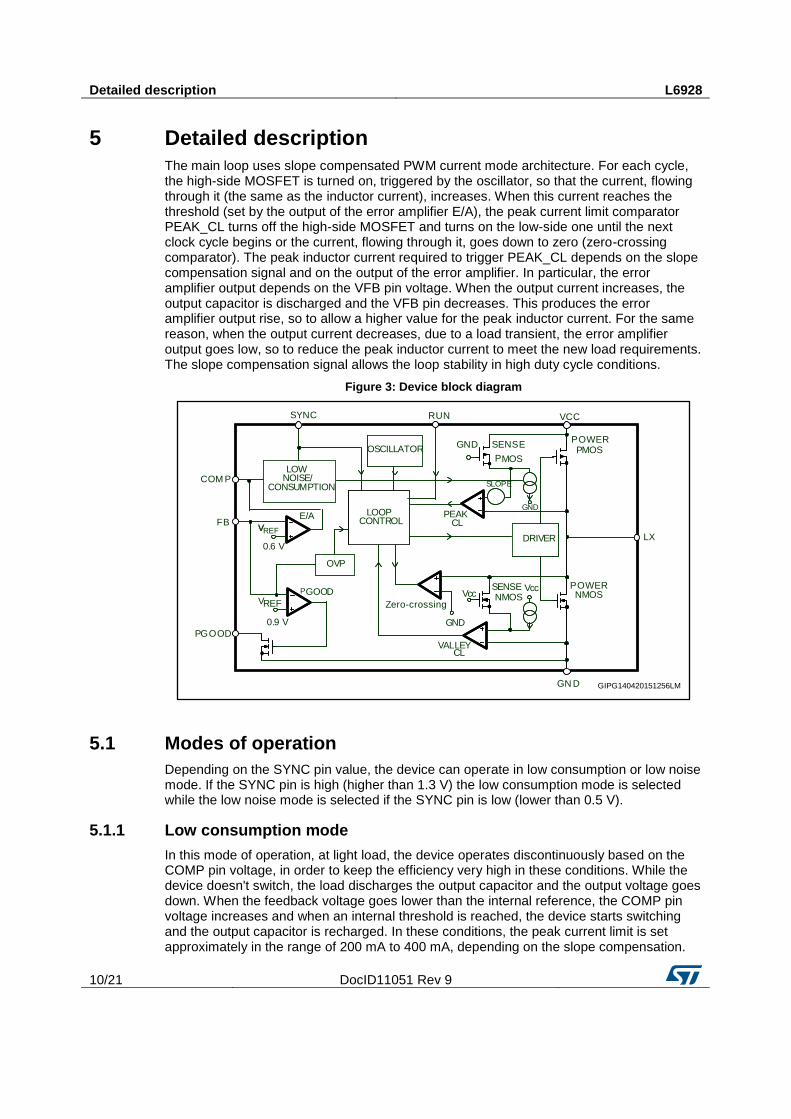
5 Detailed description
The main loop uses slope compensated PWM current mode architecture. For each cycle, the high-side MOSFET is turned on, triggered by the oscillator, so that the current, flowing through it (the same as the inductor current), increases. When this current reaches the threshold (set by the output of the error amplifier E/A), the peak current limit comparator PEAK_CL turns off the high-side MOSFET and turns on the low-side one until the next clock cycle begins or the current, flowing through it, goes down to zero (zero-crossing comparator). The peak inductor current required to trigger PEAK_CL depends on the slope compensation signal and on the output of the error amplifier. In particular, the error amplifier output depends on the VFB pin voltage. When the output current increases, the output capacitor is discharged and the VFB pin decreases. This produces the error amplifier output rise, so to allow a higher value for the peak inductor current. For the same reason, when the output current decreases, due to a load transient, the error amplifier output goes low, so to reduce the peak inductor current to meet the new load requirements. The slope compensation signal allows the loop stability in high duty cycle conditions.
Figure 3: Device block diagram
5.1 Modes of operation
Depending on the SYNC pin value, the device can operate in low consumption or low noise mode. If the SYNC pin is high (higher than 1.3 V) the low consumption mode is selected while the low noise mode is selected if the SYNC pin is low (lower than 0.5 V).
5.1.1 Low consumption mode
In this mode of operation, at light load, the device operates discontinuously based on the COMP pin voltage, in order to keep the efficiency very high in these conditions. While the device doesn't switch, the load discharges the output capacitor and the output voltage goes down. When the feedback voltage goes lower than the internal reference, the COMP pin voltage increases and when an internal threshold is reached, the device starts switching and the output capacitor is recharged. In these conditions, the peak current limit is set approximately in the range of 200 mA to 400 mA, depending on the slope compensation.

L6928 Detailed description
DocID11051 Rev 9 11/21
The feedback pin increases and, when it reaches a value slightly higher than the reference voltage, the output of the error amplifier goes down until a clamp is activated. At this point, the device stops switching. In this phase, the internal circuitries are off, so to reduce the device consumption down to a typical value of 25 μA.
5.1.2 Low noise mode
If the low frequencies of the low consumption mode are undesirable, the low noise mode can be selected. In low noise mode, the efficiency is a little bit lower compared with the low consumption mode in very light load conditions but for medium and high load currents the efficiency values are very similar. Basically, the device switches with its internal free running frequency of 1.4 MHz. Obviously, in very light load conditions, the device could skip some cycles in order to keep the output voltage in regulation.
5.1.3 Synchronization
The device can also be synchronized by an external signal from 1 MHz up to 2 MHz. In this case the low noise mode is automatically selected. The device skips some cycles in very light load conditions. The internal synchronization circuit is inhibited in short-circuit and overvoltage conditions in order to keep the protection effective.
5.2 Short-circuit protection
During the device operation, the inductor current increases during the high-side turn-on phase and decreases during the high-side turn-off phase based on the following equations:
Equation 1:
Equation 2:
In strong overcurrent or short-circuit conditions, the VOUT can be very close to zero. In this case ΔION increases and ΔIOFF decreases. When the inductor peak current reaches the current limit, the high-side MOSFET turns off and so the TON is reduced down to the minimum value (250 ns typ.) in order to reduce as much as possible ΔION. Anyway, if VOUT is low enough, the inductor peak current increases furtherly because during the TOFF the current decays very slowly. Due to this reason a second protection, fixing the maximum inductor valley current, has been introduced. This protection doesn't allow the high-side MOSFET to turn on if the current, flowing through the inductor, is higher than a specified threshold (valley current limit). Basically the TOFF increases as much as required to bring the inductor current down to this threshold. So, the maximum peak current in worst case conditions is:
Equation 3:
Where IPEAK is the valley current limit (1.4 A typ.) and TON_MIN is the minimum TON of the high-side MOSFET.
ΔION
VIN VOUT–( )
L---------------------------------- TON
.=
ΔIOFF
VOUT
L------------------- TOFF= .( )
IPEA K IVALL EY
VIN
L--------- TON _MIN+= .
Detailed description L6928
12/21 DocID11051 Rev 9
5.3 Slope compensation
In current mode architecture, when the duty cycle of the application is higher than approximately 50%, a pulse-by-pulse instability (so-called subharmonic oscillation) can occur. In these conditions, to allow loop stability, a slope compensation is present by reducing the current flowing through the inductor to trigger the COMP comparator (with a fixed value for the COMP pin voltage). With a given duty cycle higher than 50%, the stability problem is particularly present with a higher input voltage (due to the increased current ripple across the inductor), so the slope compensation effect increases as the input voltage increases. From an application point of view, the final effect is that the peak current limit depends both on the duty cycle (if higher than approximately 40%) and on the input voltage.
5.4 Loop stability
Since the device is developped by a current mode architecture, the loop stability is usually not an issue. For most of applications, a 220 pF connected between the COMP pin and ground can guarantee the stability. Very low ESR capacitors are used for the output filter, such as multilayer ceramic capacitors, the zero introduced by the capacitor itself can shift to very high frequency and the transient loop response could be affected. A series resistor added to the 220 pF capacitor can solve this problem. The right value for the resistor (in the range of 50 k) can be given by checking the load transient response of the device. Basically, the output voltage has to be checked at the scope after the load steps required by the application. In case of stability problems, the output voltage could oscillate before than the regulated value is reached after a load step.

L6928 Additional features and description
DocID11051 Rev 9 13/21
6 Additional features and description
6.1 Dropout operation
The Li-Ion battery voltage ranges from approximately 3 V and 4.1 V to 4.2 V (depending on the anode material). If the regulated output voltage is from 2.5 V and 3.3 V, close to the end of the battery life, the battery voltage goes down to the regulated one. In this case the device stops switching, working at 100% of duty cycle, so minimizing the dropout voltage and the device losses.
6.2 PGOOD
A Power Good output signal is available. The VFB pin is internally connected to a comparator with a threshold set at 90% of the reference voltage (0.6 V). Since the output voltage is connected to the VFB pin by a resistor divider, when the output voltage goes lower than the regulated value, the VFB pin voltage goes lower than 90% of the internal reference value. The internal comparator is triggered and the PGOOD pin is pulled down. The pin is an open drain output and so, a pull-up resistor should be connected to him. If the feature is not required, the pin can be left floating.
6.3 Adjustable output voltage
The output voltage can be adjusted by an external resistor divider from a minimum value of 0.6 V up to the input voltage. The output voltage value is given by the below equation:
Equation 4:
6.4 OVP (overvoltage protection)
The device has an internal overvoltage protection circuit to protect the load. If the voltage on the feedback pin goes higher than an internal threshold set 10% (typ.) higher than the reference voltage, the low-side power MOSFET turns on until the feedback voltage goes lower than the reference one. During the overvoltage circuit intervention, the zero-crossing comparator is disabled so that the device is also able to sink current.
6.5 Thermal shutdown
The device has also a thermal shutdown protection active when the junction temperature reaches 150 °C. In this case both the high-side MOSFET and the low-side turn off. Once the junction temperature goes back lower than 95 °C, the device restarts the normal operation.
VOUT 0.6 1R2
R1
-------= . ( + )

Package information L6928
14/21 DocID11051 Rev 9
7 Package information
In order to meet environmental requirements, ST offers these devices in different grades of ECOPACK® packages, depending on their level of environmental compliance. ECOPACK® specifications, grade definitions and product status are available at: www.st.com. ECOPACK® is an ST trademark.

L6928 Package information
DocID11051 Rev 9 15/21
7.1 TSSOP8 package information
Figure 4: TSSOP8 package outline
7113595_rev.2

Package information L6928
16/21 DocID11051 Rev 9
Table 6: TSSOP8 package mechanical data
Dim. mm
Min. Typ. Max.
A
1.10
A1
0.15
A2 0.75 0.85 0.95
b 0.22
0.40
c 0.08
0.23
D 2.80 3.00 3.20
E 4.65 4.90 5.15
E1 2.80 3.00 3.10
e
0.65
L 0.40 0.60 0.80
L1
0.95
L2
0.25
k 0
8
ccc
0.10
Dimensions D and E1 don't include mold flash or protrusions. Mold flash or protrusions do not exceed 0.15 mm per side.

L6928 Package information
DocID11051 Rev 9 17/21
7.2 VFQFPN8 package information
Figure 5: VFQFPN8 package outline
Top view
Side view
Bottom view
7426334 rev8
Package information L6928
18/21 DocID11051 Rev 9
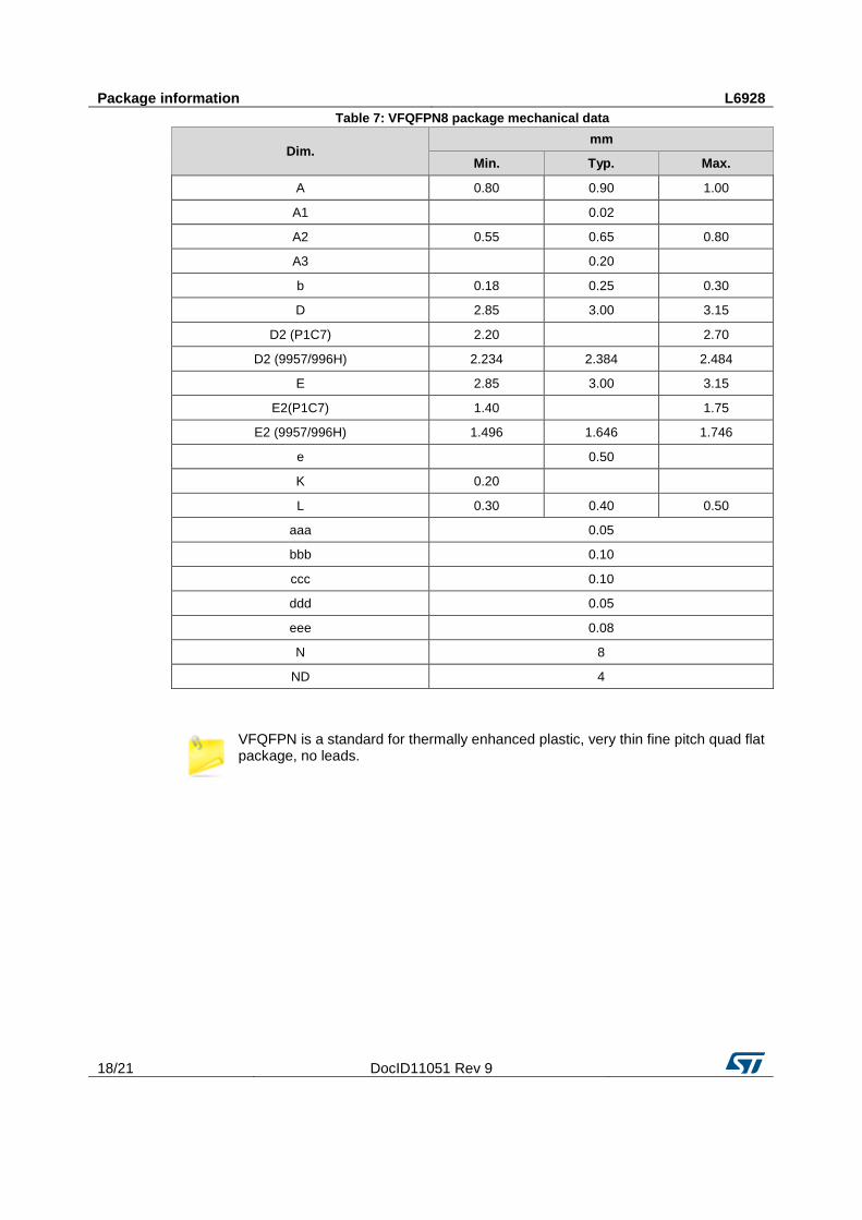
Table 7: VFQFPN8 package mechanical data
Dim. mm
Min. Typ. Max.
A 0.80 0.90 1.00
A1
0.02
A2 0.55 0.65 0.80
A3
0.20
b 0.18 0.25 0.30
D 2.85 3.00 3.15
D2 (P1C7) 2.20
2.70
D2 (9957/996H) 2.234 2.384 2.484
E 2.85 3.00 3.15
E2(P1C7) 1.40
1.75
E2 (9957/996H) 1.496 1.646 1.746
e
0.50
K 0.20
L 0.30 0.40 0.50
aaa 0.05
bbb 0.10
ccc 0.10
ddd 0.05
eee 0.08
N 8
ND 4
VFQFPN is a standard for thermally enhanced plastic, very thin fine pitch quad flat package, no leads.

L6928 Package information
DocID11051 Rev 9 19/21
Figure 6: VFQFPN8 recommended footprint

Revision history L6928
20/21 DocID11051 Rev 9
8 Revision history Table 8: Document revision history
Date Revision Changes
07-Oct-2004 1 Initial release.
04-Feb-2005 2 Changed from product preview to final datasheet.
27-Nov-2005 3 Updated Table 5. Electrical characteristics. Added
VFQFPN8 package and new part numbers.
27-Oct-2006 4 Added RthJA for VFQFPN8 in Table 3.
22-Aug-2007 5 Updated order code table.
11-Apr-2011 6 Updated TSSOP8 package information and figure 4.
20-Dec-2011 7 Updated figure 1.
Added pin connection figure.
21-Apr-2015 8 Deleted footnote 2 in table 5.
26-Oct-2016 9 Updated Table 5: "Electrical characteristics".
L6928
DocID11051 Rev 9 21/21
IMPORTANT NOTICE – PLEASE READ CAREFULLY
STMicroelectronics NV and its subsidiaries (“ST”) reserve the right to make changes, corrections, enhancements, modifications , and improvements to ST products and/or to this document at any time without notice. Purchasers should obtain the latest relevant information on ST products before placing orders. ST products are sold pursuant to ST’s terms and conditions of sale in place at the time of order acknowledgement.
Purchasers are solely responsible for the choice, selection, and use of ST products and ST assumes no liability for application assistance or the design of Purchasers’ products.
No license, express or implied, to any intellectual property right is granted by ST herein.
Resale of ST products with provisions different from the information set forth herein shall void any warranty granted by ST for such product.
ST and the ST logo are trademarks of ST. All other product or service names are the property of their respective owners.
Information in this document supersedes and replaces information previously supplied in any prior versions of this document.
© 2016 STMicroelectronics – All rights reserved