mp8796b 16v, 30a, scalable, digital, synchronous step-down
TRANSCRIPT

MP8796B 16V, 30A, Scalable, Digital, Synchronous
Step-Down Converter with PMBus
MP8796B Rev. 1.0 www.MonolithicPower.com 1 1/19/2020 MPS Proprietary Information. Patent Protected. Unauthorized Photocopy and Duplication Prohibited. © 2020 MPS. All Rights Reserved.
DESCRIPTION The MP8796B is a fully integrated, PMBus-compatible, high-frequency, synchronous buck converter. The MP8796B offers a very compact solution that achieves up to 30A of output current per phase with excellent load and line regulation over a wide input supply range. The MP8796B operates at high efficiency over a wide output current load range.
The PMBus interface provides converter configurations and key parameter monitoring.
The MP8796B adopts MPS’s proprietary, multi-phase constant-on-time (MCOT) control, which provides fast transient response and eases loop stabilization. The MCOT control scheme also allows multiple MP8796B devices to be connected in parallel with excellent current sharing and phase interleaving for high-current applications.
Fully integrated protection features include over-current protection (OCP), over-voltage protection (OVP), under-voltage protection (UVP), and over-temperature protection (OTP).
The MP8796B requires a minimal number of readily available, standard external components, and is available in a TQFN-25 (4mmx5mm) package.
FEATURES
PMBus 1.3 Compliant Scalable Multi-Phase Operation 3.1V to 16V with External 3.3V VCC Bias,
4V to 16V with Internal Bias or External 3.3V VCC Bias
30A Continuous Output Current per Phase Low RDS(ON) Integrated Power MOSFETs Lossless, Accurate On-Die Current Sensing Adaptive COT for Ultra-Fast Transient
Response Stable with Zero-ESR Output Capacitors 0.5% Reference Voltage Over 0°C to +70°C
Junction Temperature Range Output Voltage True Remote Sense Output Adjustable from 0.4V to 0.9 x VIN Up
to 5.5V Max Output Voltage/Current, Input Voltage, and
Junction Temperature Reporting Built-In MTP to Store Custom
Configurations Configurable via PMBus
o Output Voltage o Output Current Limit o Selection of Pulse Skip or Forced CCM
Operation o Soft-Start Time o Selection of Switching Frequency from
400kHz, 600kHz, 800kHz, or 1000kHz o Selection of Hiccup or Latch-Off Mode
for OCP, OVP, and OTP o Ramp Compensation
Available in a TQFN-25 (4mmx5mm) Package
APPLICATIONS Telecom and Networking Systems Base Stations Servers
All MPS parts are lead-free, halogen-free, and adhere to the RoHS directive. For MPS green status, please visit the MPS website under Quality Assurance. “MPS”, the MPS logo, and “Simple, Easy Solutions” are trademarks of Monolithic Power Systems, Inc. or its subsidiaries.

MP8796B – 16V, 30A, SYNCHRONOUS STEP-DOWN CONVERTER WITH PMBUS
MP8796B Rev. 1.0 www.MonolithicPower.com 2 1/19/2020 MPS Proprietary Information. Patent Protected. Unauthorized Photocopy and Duplication Prohibited. © 2020 MPS. All Rights Reserved.
TYPICAL APPLICATION CIRCUITS Single-Phase Operation
SDA
ALT
ENFB
BSTIN SW
VIN
MP8796B
VOUT
CIN
CVCC
CBSTL1
COUT
EN
PG
RADDRSCL
R1
RREF
CCDRV
R2
Two-Phase Operation
EN
FB
BSTIN SW
VIN
MP8796B
VOUT
CIN
CVCC
CBSTL1
EN
PG
RADDR
SDA
ALT
ENFB
BSTIN SW
MP8796B
CIN1
L2
SCL RADDR1
R1
CBST1
CVCC1
RREF
RREF1
COUT
CDRV
CDRV1

MP8796B – 16V, 30A, SYNCHRONOUS STEP-DOWN CONVERTER WITH PMBUS
MP8796B Rev. 1.0 www.MonolithicPower.com 3 1/19/2020 MPS Proprietary Information. Patent Protected. Unauthorized Photocopy and Duplication Prohibited. © 2020 MPS. All Rights Reserved.
ORDERING INFORMATION
Part Number* Package Top Marking Note MSL
Rating MP8796BGVT- xxxx** TQFN-25 (4mmx5mm) See Below
1 MP8796BGVT - 0000 TQFN-25 (4mmx5mm) See Below Single phase 0.92V
output EVKT-MP8796B-30A Evaluation kit See Below EVKT-MP8796B-180A Evaluation kit See Below
* For Tape & Reel, add suffix –Z (e.g. MP8796BGVT-xxxx**–Z). ** “xxxx” is the configuration code identifier for the register settings stored in the MTP. The default number is
“0000”. Each “x” is a hexadecimal value between 0 and F. See table 7 and 8 on page 51 for the detailed configuration and register value. For customized configurations, please contact MPS Field Application Engineer to
assign a 4-digit suffix code.
TOP MARKING
MPS: MPS prefix Y: Year code WW: Week code M8796B: Part number LLLLLL: Lot number
EVALUATION KIT EVKT-MP8796B Contents (items below can be ordered separately, and the GUI installation file and supplemental documents can be downloaded from the MPS website):
EVKT-MP8796B-30A: Single-phase
Item # Part Number Item Quantity
1 EV8796B-V-1Phase-00A MP8796B single phase evaluation board 1
2 EVKT-USBI2C-02 Includes one USB to I2C communication interface device, one USB cable, and one ribbon cable
1
EVKT-MP8796B-180A: Six-phase
Item # Part Number Item Quantity
1 EV8796B-V-6Phase-00A MP8796B six-phase evaluation board 1
2 EVKT-USBI2C-02 Includes one USB to I2C communication interface device, one USB cable, and one ribbon cable
1
Order directly from monolithicpower.com or our distributors.

MP8796B – 16V, 30A, SYNCHRONOUS STEP-DOWN CONVERTER WITH PMBUS
MP8796B Rev. 1.0 www.MonolithicPower.com 4 1/19/2020 MPS Proprietary Information. Patent Protected. Unauthorized Photocopy and Duplication Prohibited. © 2020 MPS. All Rights Reserved.
Evaluation Board
Load
Ribbon Cable
GUI
Output
Input
USB to I2C Communication Interface EVKT-USBI2C-02
Input Power Supply
USB Cable
Load
Figure 1: EVKT-MP8796B Kit Set-Up
PACKAGE REFERENCE
TOP VIEW
IN
SW
PGND
CTRL
SW
15
16
25
IN
5 6
SCL ALT# PASS TAKESDAVDRV
PGND14
987 10 12
SET
BST ADDR PS#VOSNS+ ISUMIREFAGNDVCC VOSNS-
PG
11
PGND
13
2
4
3
2122 192024 23
TQFN-25 (4mmx5mm)

MP8796B – 16V, 30A, SYNCHRONOUS STEP-DOWN CONVERTER WITH PMBUS
MP8796B Rev. 1.0 www.MonolithicPower.com 5 1/19/2020 MPS Proprietary Information. Patent Protected. Unauthorized Photocopy and Duplication Prohibited. © 2020 MPS. All Rights Reserved.
PIN FUNCTIONS Pin # Name Description
1, 16 IN Supply voltage. IN supplies power to the internal MOSFET and regulator. Use an input capacitor to decouple the input rail. Use wide PCB traces and multiple vias to make the connection.
2, 3 SW Switch output. Connect SW to the inductor and bootstrap capacitor. SW is driven up to VIN by the high-side switch during the PWM duty cycle on time. The inductor current drives SW negative during the off time. Use wide PCB traces to make the connection.
4, 14, 15 PGND System ground. PGND is the reference ground of the regulated output voltage, and requires careful consideration during PCB layout. Connect PGND with wide PCB traces.
5 VDRV
Decoupling input pin for 3.3V driver power supply. Decouple VDRV with a minimum 1µF ceramic capacitor, placed as close to VDRV as possible. X7R or X5R-grade dielectric ceramic capacitors are recommended. VDRV accepts a 3.3V external bias. If no 3.3V external bias is provided, connect VDRV to VCC through a 2Ω to 10Ω resistor.
6 SCL PMBus clock.
7 SDA PMBus data.
8 ALT# PMBus alert pin. ALT# is active low. A pull-up resistor connected to 3.3V is required if the ALT# function is needed.
9 CTRL PMBus control pin. CTRL is a digital input pin that turns the regulator on or off with proper ON_OFF_CONFIG (02h) configuration. Drive CTRL high to turn on the regulator; drive it low to turn off the regulator. Do not float CTRL.
10 PG
Power good output. The output of PG is an open-drain signal. PG requires a pull-up resistor connected to a DC voltage to indicate high if the output voltage is above 90% of the nominal voltage. There is a PGOOD delay from low to high. PG must be pulled high to ensure proper operation.
11 PASS Passes RUN signals to the next phase.
12 TAKE
Receives RUN signals from the previous phase. TAKE is used for master detection during the device’s initial power-up. For the master phase, TAKE must be pulled high through a resistor. For the slave phase, TAKE is connected to the PASS of the previous phase.
13 SET PWM signal. SET turns the high-side MOSFET on when a RUN signal is present. For multi-phase operation, tie the SET pins of all phases together.
17 PS# Phase shedding. With proper PMBus setting, pull PS# high to enable a slave phase. Pull it low to disable a slave phase. Connect PS# of the master phase to AGND.
18 ADDR PMBus slave address setting pin. Connect a resistor from ADDR to AGND to set the address of this device.
19 ISUM Current-sense output. For single-phase operation, keep ISUM floating. For multi-phase operation, tie the ISUM pins of all phases together for current sharing.
20 IREF Reference current generator amplifier output. Connect a 60.4kΩ or 180kΩ resistor with 1% or greater accuracy to IREF.
21 VOSNS- Output voltage sense negative return. VOSNS- is tied directly to the GND sense point of the load. Connect VOSNS- to AGND if the remote sense is not used.
22 VOSNS+ Output voltage sense positive return. Connect VOSNS+ to the output voltage sense positive side to provide feedback voltage to the system. Avoid vias on the VO traces.
23 AGND Analog ground. Select AGND as the control-circuit reference point.

MP8796B – 16V, 30A, SYNCHRONOUS STEP-DOWN CONVERTER WITH PMBUS
MP8796B Rev. 1.0 www.MonolithicPower.com 6 1/19/2020 MPS Proprietary Information. Patent Protected. Unauthorized Photocopy and Duplication Prohibited. © 2020 MPS. All Rights Reserved.
PIN FUNCTIONS (continued) Pin # Name Description
24 VCC
Internal 3.3V LDO output. VCC powers the analog and digital control circuits. Decouple VCC with a minimum 4.7µF ceramic capacitor, placed as close to VCC as possible. X7R or X5R-grade dielectric ceramic capacitors are recommended. During MTP programming, a 5V voltage with a 300ms period may be observed on VCC. The VCC pin does not accept external voltage bias. For multi-phase applications, connect the VCC pins of all phases together.
25 BST Bootstrap. A capacitor connected between SW and BS is required to form a floating supply across the high-side switch driver.
ABSOLUTE MAXIMUM RATINGS (1) Supply voltage (VIN) ...................................... 18V VIN - VSW (DC) ................................ -0.3V to +18.3V VIN - VSW (25nc) .................................... -5V to +25V VSW (DC) ........................................ -0.3V to +18.3V VSW (25ns)
(2) ......................................... -5V to +25V VBST ............................................................. 22.3V VBST - VSW (25ns)
(2) ............................................. 5V VCC, VDRV ..................................................... 4.5V VCC (1s)
(3) .......................................................... 6V All other pins ................................ -0.3V to +4.3V All other pins (1s)
(3) ........................................... 6V Junction temperature ................................ 170°C Lead temperature ...................................... 260°C Storage temperature ................. -65°C to +170°C
ESD Rating Human-body model (HBM) ......................... ±1kV Charged-device model (CDM)................... ±2kV
Recommended Operating Conditions (4) Supply voltage (VIN) ............................ 4V to 16V Output voltage (VOUT) ...................... 0.6V to 5.5V External VDRV bias ........................... 2.9V to 3.6V Operating junction temp (TJ) ..... -40°C to +125°C
Thermal Resistance (5) θJB θJC_TOP TQFN-25 (4mmx5mm) ......... 1.8 ....... 6.3 ... °C/W
Notes:
1) Exceeding these ratings may damage the device. 2) Specified by design. Measured using a differential
oscilloscope probe. 3) Voltage rating during MTP programming. 4) The device is not guaranteed to function outside of its
operating conditions. 5) θJB is the thermal resistance from the junction to the board
around the PGND soldering point. θJC_TOP is the thermal resistance from the junction to the top of the package.

MP8796B – 16V, 30A, SYNCHRONOUS STEP-DOWN CONVERTER WITH PMBUS
MP8796B Rev. 1.0 www.MonolithicPower.com 7 1/19/2020 MPS Proprietary Information. Patent Protected. Unauthorized Photocopy and Duplication Prohibited. © 2020 MPS. All Rights Reserved.
ELECTRICAL CHARACTERISTICS VIN = 12V, TJ = -40°C to +125°C(7), typical value is tested at TJ = 25°C, unless otherwise noted.
Parameters Symbol Condition Min Typ Max Units
VIN Supply Current
Supply current (quiescent) IIN VCTRL = 0V 2.5 4 mA
MOSFET
RDS(ON) RONHS 4.4
mΩ RONLS 1.5
Switch leakage SWLKG_HS SW = 0V 0.1 10
μA SWLKG_LS SW = 12V 1 20
Output Current Limit
Output current limit (inductor valley)
ILIM_VALLEY D7h = 0x14 27 30 33 A
Min output current limit (inductor valley) programmable value (6)
ILIM_VALLEY_MIN 1.5 A
Max output current limit (inductor valley) programmable value
ILIM_VALLEY_MAX 36 40 44 A
Min output over-current programmable value (6)
ILIM_DC_MIN 3 A
Min output over-current warning programmable value (6)
3 A
Low-side negative current limit in OVP
ILIM_NEG_OVP D5h[2] = 1b’0 -13 A
D5h[2] = 1b’1 -20 A
Low-side negative current limit in OSM (6)
ILIM_NEG_OSM -10 A
Frequency and Timer
Switching frequency (6) fSW
VO = 1V, IO = 0A, TA = 25°C, (D2h[2:1] = 2b’00)
280 400 520 kHz
VO = 1V, IO = 0A, TA = 25°C, (D2h[2:1] = 2b’01)
480 600 720 kHz
VO = 1V, IO = 0A, TA = 25°C, (D2h[2:1] = 2b’10)
680 800 920 kHz
VO = 1V, IO = 0A, TA = 25°C, (D2h[2:1] = 2b’11)
850 1000 1150 kHz
Minimum on time (6) tON_MIN fSW = 1000kHz, VO = 0.6V 50 ns
Minimum off time (6) tOFF_MIN VFB = 580mV 220 ns

MP8796B – 16V, 30A, SYNCHRONOUS STEP-DOWN CONVERTER WITH PMBUS
MP8796B Rev. 1.0 www.MonolithicPower.com 8 1/19/2020 MPS Proprietary Information. Patent Protected. Unauthorized Photocopy and Duplication Prohibited. © 2020 MPS. All Rights Reserved.
ELECTRICAL CHARACTERISTICS (continued) VIN = 12V, TJ = -40°C to +125°C(7), typical value is tested at TJ = 25°C, unless otherwise noted.
Parameters Symbol Condition Min Typ Max Units
Output Over-Voltage and Under-Voltage Protection (OVP, UVP)
OVP threshold VOVP Default setting (D4h[1:0] = 2b’00) 112% 115% VREF
UVP threshold VUVP Default setting (D9h[3:2] = 2b’10) 76% 79% 83% VREF
Max programmable OVP threshold
VOVP_MAX D4h[1:0] = 2b’11 127% 130% 133% VREF
Min programmable OVP threshold
VOVP_MIN D4h[1:0] = 2b’00 112% 115% VREF
OVP threshold resolution Per LSB 5% VREF
Max programmable UVP threshold
VUVP_MAX D9h[3:2] = 2b’11 81% 84% 88% VREF
Min programmable UVP threshold
VUVP_MIN D9h[3:2] = 2b’00 66% 69% 72% VREF
UVP threshold resolution Per LSB 5% VREF
OSM threshold rising VOSM_RISE EAh[9] = 1b’0
104.8% VREF
OSM threshold falling VOSM_FALL 102.2% VREF
CTRL
Input high voltage VIH_CTRL 2.15 V
Input low voltage VIL_CTRL 1.20 V
ADC (6)
Input voltage range 0 1.28 V
ADC resolution 10 Bits
DNL 1 LSB
Sample rate 3 kHz
DAC (Feedback Voltage)
Range 512 600 672 mV
Feedback accuracy VFB 21h = 0x012C, D1h[1:0] = 2b’00 594 600 606 mV
Resolution Per LSB 2 mV
Output voltage slew rate Default setting (DAh[3:0] = 4b’0000)
20 µs/
2mV
Minimum output voltage slew rate
DAh[3:0] = 4b’1111 30 40 50 µs/
2mV
Maximum output voltage slew rate
DAh[3:0] = 4b’0000 20 µs/
2mV
Maximum feedback voltage with margin (6)
VFB_MG_HIGH_
MAX 672 mV
Minimum feedback voltage with margin (6)
VFB_MG_LOW_
MIN 512 mV
Feedback voltage with margin high (6)
VFB_MG_HIGH 672 mV
Feedback voltage with margin low (6)
VFB_MG_LOW 512 mV

MP8796B – 16V, 30A, SYNCHRONOUS STEP-DOWN CONVERTER WITH PMBUS
MP8796B Rev. 1.0 www.MonolithicPower.com 9 1/19/2020 MPS Proprietary Information. Patent Protected. Unauthorized Photocopy and Duplication Prohibited. © 2020 MPS. All Rights Reserved.
ELECTRICAL CHARACTERISTICS (continued) VIN = 12V, TJ = -40°C to +125°C(7), typical value is tested at TJ = 25°C, unless otherwise noted.
Parameters Symbol Condition Min Typ Max Units
Soft Start and Turn-On Delay
Soft-start time tSS 61h[2:0] = 3b’001 1.7 2.3 3.0 ms
Min programmable soft-start time (6)
tSS_MIN 61h[2:0] = 3b’000 1 ms
Max programmable soft-start time (6)
tSS_MAX 16 ms
Turn-on delay tON_DELAY 60h = 0x0001 3.9 4.5 5.1 ms
Min turn-on delay (6) tON_DELAY_MIN 60h = 0x0000 0 ms
Max turn-on delay (6) tON_DELAY_MAX 60h = 0x0100 1024 ms
Error Amplifier
Feedback current IFB VFB = VREF 50 100 nA
Soft Shutdown
Soft shutdown discharge MOSFET
RON_DISCH TJ = 25°C 60 120 Ω
Under-Voltage Lockout (UVLO)
VCC under-voltage lockout threshold rising
VCCVth_Rise 2.60 2.75 2.9 V
VCC under-voltage lockout threshold falling
VCCVth_Fall 2.35 2.50 2.65 V
VCC output voltage VCC 3.10 3.25 3.40 V
Min input programmable turn-on voltage
VIN_ON_MIN VCC = 3.3V 2.65 2.90 3.1 V
Max input programmable turn-on voltage
VIN_ON_MAX 16 16.5 17 V
Min input programmable turn-off voltage (6)
VIN_OFF_MIN VCC = 3.3V 2.5 2.75 3 V
Max input programmable turn-off voltage
VIN_OFF_MAX 15.75 V
VDRV under-voltage lockout rising threshold VDRVVth_Rise 2.55 2.75 2.95 V
VDRV under-voltage lockout falling threshold VDRVVth_Fall 2.15 2.35 2.55 V
Power Good (PG)
Power good high threshold PGVth_Hi_RiseFB from low to high, default setting (D9h[1:0] = 2b’01)
91% 94% 97% VREF
Power good low threshold PGVth_Lo_Rise
FB from low to high, default setting (D4h[1:0] = 2b’00)
112% 115% 118% VREF
PGVth_Lo_FallFB from high to low, default setting (D9h[3:2] = 2’b10)
76% 79% 83% VREF
Power good low-to-high delay PGTd Default setting (D1h[5:2] = 4b’0000)
1.6 2.0 2.4 ms
Power good sink current capability VPG IPG = 10mA 0.3 V

MP8796B – 16V, 30A, SYNCHRONOUS STEP-DOWN CONVERTER WITH PMBUS
MP8796B Rev. 1.0 www.MonolithicPower.com 10 1/19/2020 MPS Proprietary Information. Patent Protected. Unauthorized Photocopy and Duplication Prohibited. © 2020 MPS. All Rights Reserved.
ELECTRICAL CHARACTERISTICS (continued) VIN = 12V, TJ = -40°C to +125°C(7), typical value is tested at TJ = 25°C, unless otherwise noted.
Parameters Symbol Condition Min Typ Max Units
Power Good (PG)
Power good leakage current IPG_LEAK VPG = 3V 1.5 2.3 µA
Power good low-level output voltage
VOL_100 VIN = 0V, pull PGOOD up to 3.3V through a 100kΩ resistor, TJ = 25°C
600 720
mV
VOL_10 VIN = 0V, pull PGOOD up to 3.3V through a 10kΩ resistor, TJ = 25°C
700 820
Thermal Protection (TP)
TP fault rising threshold (6) TSD_Rise Default setting (4Fh = 0x0091) 145 °C
TP fault falling threshold (6) TSD_Fall Default setting (4Fh = 0x007D and D6h[2:1] = 2b’00)
125 °C
Min TP fault temp (6) TSD_WARN_MIN 35 °C
Max TP fault temp (6) TSD_WARN_MAX 165 °C
TP warning rising threshold (6) TWARN_Rise Default setting (51h = 0x0078) 120 °C
TP warning falling threshold (6) TWARN_Fall Default setting (51h = 0x0078, D6h[2:1] = 2b’00)
100 °C
Min TP warning temp (6) TSD_WARN_MIN 35 °C
Max TP warning temp (6) TSD_WARN_MAX 160 °C
Monitoring Parameters
Min output voltage monitor range (6)
MVOUT_RANGE 0 V
Max output voltage monitor range (6)
MVOUT_RANGE 5.5 V
Output voltage monitor accuracy (6)
MVOUT_ACC VO = 0.6V to 2.5V -2% 0.6 +2% V
Output voltage monitor accuracy (6)
MVOUT_ACC VO = 2.5V to 5.5V 50 50 mV
Output voltage bit resolution 1.25 mV
Output current monitor accuracy
MIOUT_ACC VO = 1.2V, fSW = 800kHz, IO = 30A
-2.5 +2.5 A
Output current monitor accuracy (6)
MIOUT_ACC 3A ≤ IO ≤ 30A -2.5 +2.5 A
Output current bit resolution (6) 62.5 mA
Min input voltage monitor (6) MIN_RANGE 2.5 V
Max input voltage monitor (6) MIN_RANGE 18 V
Input voltage monitor accuracy MIN_ACC -2% 12 +2% V
Input voltage bit resolution (7) 25 mV

MP8796B – 16V, 30A, SYNCHRONOUS STEP-DOWN CONVERTER WITH PMBUS
MP8796B Rev. 1.0 www.MonolithicPower.com 11 1/19/2020 MPS Proprietary Information. Patent Protected. Unauthorized Photocopy and Duplication Prohibited. © 2020 MPS. All Rights Reserved.
ELECTRICAL CHARACTERISTICS (continued) VIN = 12V, TJ = -40°C to +125°C(7), typical value is tested at TJ = 25°C, unless otherwise noted.
Parameters Symbol Condition Min Typ Max Units
PMBus DC Characteristics (SDA, SCL, ALT#, CTRL) (6)
Input high voltage VIH 2.1 V Input low voltage VIL 0.8 V Output low voltage VOL IOL = 1mA 0.4 V Input leakage current ILEAK SDA, SCL, ALT# = 3.3V -10 +10 µA Maximum voltage (SDA, SCL, ALT#, CTRL) VMAX
Transient voltage including ringing -0.3 3.3 +3.6 V
Pin capacitance on SDA,SCL CPIN 10 pF
PMBus Timing Characteristics (7)
Min operating frequency 10 kHzMax operating frequency 1000 kHzBus free time Between stop and start condition 4.7 µs Holding time 4.0 µs Repeated start condition set-up time 4.7 µs
Stop condition set-up time 4.0 µs Data hold time 300 ns Data set-up time 250 ns Clock low timeout 25 35 ms Clock low period 4.7 µs Clock high period 4.0 50 µs Clock/data fall time 300 ns Clock/data rise time 1000 ns
Notes: 6) Guaranteed by design. 7) Guaranteed by design; not tested in production. The parameter is tested during parameter characterization.

MP8796B – 16V, 30A, SYNCHRONOUS STEP-DOWN CONVERTER WITH PMBUS
MP8796B Rev. 1.0 www.MonolithicPower.com 12 1/19/2020 MPS Proprietary Information. Patent Protected. Unauthorized Photocopy and Duplication Prohibited. © 2020 MPS. All Rights Reserved.
TYPICAL PERFORMANCE CHARACTERISTICS VIN=12V, VOUT=1.2V, TA=+25°C, unless otherwise noted.
Load Regulation VIN = 12V, CCM, fSW = 1000kHz
fSW vs. IOUT VIN = 12V, CCM
1.195
1.197
1.199
1.201
1.203
1.205
1.207
1.209
1.211
1.213
1.215
0 5 10 15 20
VO
(V)
IO (A)
Pulse SkipCCM
0
100
200
300
400
500
600
700
800
900
1000
0 10 20 30f S
W (k
Hz)
IO (A)
1000KHz800KHz600KHz400KHz
Thermal Derating VIN = 12V, fSW = 1000kHz, TJ = 125°C, no air flow
Efficiency VIN = 12V, fSW = 1000kHz, L = 0.44μH/0.18mΩ
0
5
10
15
20
25
30
35
5 55 105
LO
AD
(A
)
AMBIENT TEMP ()
Vo=1.2VVo=2.5VVo=5V
50
55
60
65
70
75
80
85
90
95
100
0 10 20 30
EFF
ICIE
NC
Y(%
)
IO (A)
5V2.5V1.2V
MP8796B – 16V, 30A, SYNCHRONOUS STEP-DOWN CONVERTER WITH PMBUS
MP8796B Rev. 1.0 www.MonolithicPower.com 13 1/19/2020 MPS Proprietary Information. Patent Protected. Unauthorized Photocopy and Duplication Prohibited. © 2020 MPS. All Rights Reserved.
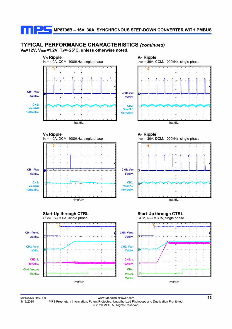
TYPICAL PERFORMANCE CHARACTERISTICS (continued) VIN=12V, VOUT=1.2V, TA=+25°C, unless otherwise noted.
VO Ripple IOUT = 0A, CCM, 1000kHz, single phase
VO Ripple IOUT = 30A, CCM, 1000kHz, single phase
CH1: VSW
5V/div.
CH2:
VOUT/AC 10mV/div.
CH1: VSW
5V/div.
CH2: VOUT/AC
10mV/div.
1μs/div. 1μs/div.
VO Ripple IOUT = 0A, DCM, 1000kHz, single phase
VO Ripple IOUT = 30A, DCM, 1000kHz, single phase
CH1: VSW
5V/div.
CH2:
VOUT/AC 10mV/div.
CH1: VSW
5V/div.
CH2: VOUT/AC
10mV/div.
4ms/div. 1μs/div.
Start-Up through CTRL CCM, IOUT = 0A, single phase
Start-Up through CTRL CCM, IOUT = 30A, single phase
CH1: VCTRL
2V/div.
CH2: VOUT
1V/div.
CH3: IL
10A/div.
CH4: VPGOOD
5V/div.
CH1: VCTRL
2V/div.
CH2: VOUT
1V/div.
CH3: IL
10A/div.
CH4:
VPGOOD
5V/div.
1ms/div. 1ms/div.

MP8796B – 16V, 30A, SYNCHRONOUS STEP-DOWN CONVERTER WITH PMBUS
MP8796B Rev. 1.0 www.MonolithicPower.com 14 1/19/2020 MPS Proprietary Information. Patent Protected. Unauthorized Photocopy and Duplication Prohibited. © 2020 MPS. All Rights Reserved.
TYPICAL PERFORMANCE CHARACTERISTICS (continued) VIN=12V, VOUT=1.2V, TA=+25°C, unless otherwise noted.
Start-Up through CTRL DCM, IOUT = 0A, single phase
Start-Up through CTRL DCM, IOUT = 30A, single phase
CH1: VCTRL
2V/div.
CH2: VOUT
1V/div.
CH3: IL
10A/div.
CH4: VPGOOD
5V/div.
CH1: VCTRL
2V/div.
CH2: VOUT
1V/div.
CH3: IL
10A/div.
CH4:
VPGOOD
5V/div. 1ms/div. 1ms/div.
Shutdown through CTRL CCM, IOUT = 0A, single phase
Shutdown through CTRL CCM, IOUT = 30A, single phase
CH1: VCTRL
2V/div.
CH2: VOUT 1V/div.
CH3: IL
10A/div.
CH4: VPGOOD
5V/div.
CH1: VCTRL
2V/div.
CH2: VOUT
1V/div.
CH3: IL
10A/div.
CH4:
VPGOOD
5V/div.
20ms/div. 20ms/div.
Shutdown through CTRL DCM, IOUT = 0A, single phase
Shutdown through CTRL DCM, IOUT = 30A, single phase
CH1: VCTRL
2V/div.
CH2: VOUT
1V/div.
CH3: IL
10A/div.
CH4: VPGOOD
5V/div.
CH1: VCTRL
2V/div.
CH2: VOUT
1V/div.
CH3: IL
10A/div.
CH4:
VPGOOD
5V/div.
20ms/div. 20ms/div.

MP8796B – 16V, 30A, SYNCHRONOUS STEP-DOWN CONVERTER WITH PMBUS
MP8796B Rev. 1.0 www.MonolithicPower.com 15 1/19/2020 MPS Proprietary Information. Patent Protected. Unauthorized Photocopy and Duplication Prohibited. © 2020 MPS. All Rights Reserved.
TYPICAL PERFORMANCE CHARACTERISTICS (continued) VIN=12V, VOUT=1.2V, TA=+25°C, unless otherwise noted.
Pre-Biased Start-Up CCM, single phase
Pre-Biased Start-Up DCM, single phase
CH1: VCTRL
2V/div.
CH2: VOUT
1V/div.
CH3: IL
10A/div.
CH4: VPGOOD
5V/div.
CH1: VCTRL
2V/div.
CH2: VOUT
1V/div.
CH3: IL
10A/div.
CH4:
VPGOOD
5V/div. 1ms/div. 1ms/div.
Load Transient IOUT = 0A to 10A, CCM, 1000kHz
Load Transient IOUT = 0A to 10A, DCM, 1000kHz
CH3: IOUT
4A/div.
CH4: VOUT
50mV/div.
CH3: IOUT
4A/div.
CH4: VOUT
50mV/div.
20μs/div. 20μs/div.
OCP CCM, single phase, latch-off mode
OCP CCM, single phase, hiccup mode
CH1: VSW
10V/div.
CH2: VPGOOD
2V/div.
CH3: IL
10A/div.
CH1: VSW
10V/div.
CH2: VPGOOD
2V/div.
CH3: IL
10A/div.
40ms/div. 40ms/div.

MP8796B – 16V, 30A, SYNCHRONOUS STEP-DOWN CONVERTER WITH PMBUS
MP8796B Rev. 1.0 www.MonolithicPower.com 16 1/19/2020 MPS Proprietary Information. Patent Protected. Unauthorized Photocopy and Duplication Prohibited. © 2020 MPS. All Rights Reserved.
TYPICAL PERFORMANCE CHARACTERISTICS (continued) VIN=12V, VOUT=1.2V, TA=+25°C, unless otherwise noted.
OCP DCM, single phase, latch-off mode OCP
DCM, single phase, hiccup mode
CH1: VSW
10V/div.
CH2: VPGOOD
2V/div.
CH3: IL
10A/div.
CH1: VSW
10V/div.
CH2: VPGOOD
2V/div.
CH3: IL
10A/div.
40ms/div. 40ms/div.
OVP DCM, single phase, hiccup mode
OVP CCM, single phase, hiccup mode
CH1: VOUT
1V/div.
CH2: VPGOOD
2V/div.
CH3: IL
10A/div.
CH1: VOUT
1V/div.
CH2: VPGOOD
2V/div.
CH3: IL
10A/div.
400μs/div. 400μs/div.
OVP DCM, single phase, latch-off mode
OVP CCM, single phase, latch-off mode
CH1: VOUT
1V/div.
CH2: VPGOOD 2V/div.
CH3: IL
10A/div.
CH1: VOUT
1V/div.
CH2: VPGOOD
2V/div.
CH3: IL
10A/div.
400μs/div. 400μs/div.

MP8796B – 16V, 30A, SYNCHRONOUS STEP-DOWN CONVERTER WITH PMBUS
MP8796B Rev. 1.0 www.MonolithicPower.com 17 1/19/2020 MPS Proprietary Information. Patent Protected. Unauthorized Photocopy and Duplication Prohibited. © 2020 MPS. All Rights Reserved.
FUNCTIONAL BLOCK DIAGRAM
ALT#
AGND
IREF
ADC
PMBusVTEMP
MS
SystemConfigureRegisters
ADDR
Hi-Z
MN1
MTP
CC2
TempSense
CC1
MN3
MN2
2MΩ
SWVIN
Comp1Gm1
RAMP
Drivers
+
- S Q
xQ
FB+
R
O R
tON Generator
OI
OneShot 2
VTEMP
-
+
VOSNS+
ControlLogic
SW
VIN
PGND
ISUM
Gm2
-
+
PS#
PG
+
ADC
SoftStart
FBMonitor
FB
ZCD
REF
MUX
PWM
ISUM
ISEN
DAC
BST
ILIM
Valley Current Limit
InOut
Blank
ISEN
REF
PASS
VDRV
CTRL
FB
VIN
VCC
IS1
VOSNS-
MasterDirection
LDO
-
FBGain
IS2
Take PassLogic
TAKE
ReferencesBias CurrentGenerator
LS Current Sense
RUN
SET
SDA
SCL
VCOMPCOMP-OUT
SET
20MHz
FB+RAMP
Slave FaultSS_RDY
Slave Fault Detect
Figure 2: Functional Block Diagram

MP8796B – 16V, 30A, SYNCHRONOUS STEP-DOWN CONVERTER WITH PMBUS
MP8796B Rev. 1.0 www.MonolithicPower.com 18 1/19/2020 MPS Proprietary Information. Patent Protected. Unauthorized Photocopy and Duplication Prohibited. © 2020 MPS. All Rights Reserved.
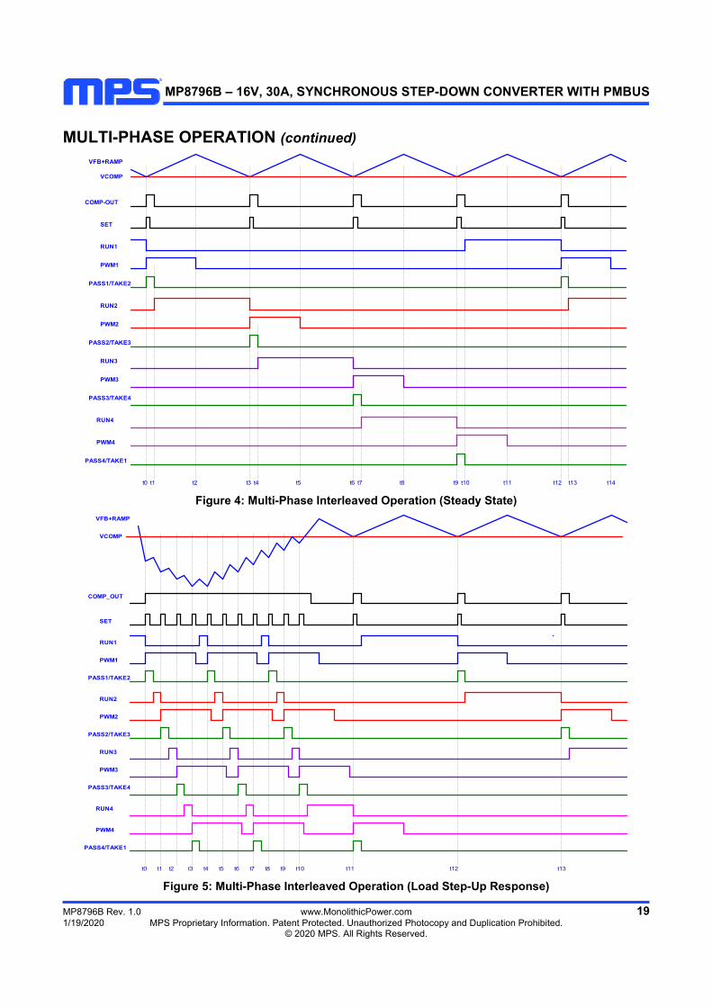
MULTI-PHASE OPERATION
SDA
ALT
EN
IN SW
VIN
MP8796B
VOUT
CVCC
L1
COUT
EN
RADDR
SCL
L2
R4
RREF
EN
IN SW
MP8796B
CVCC1
Ln
EN
IN SW
MP8796B
CVCCn
MASTER
SLAVE1
SLAVEn
BST CBST
BST CBST1
BST CBSTn
FBVOS+
VOS-
VOS+
VOS-
RADDR1 RREF1
FB VOS+
VOS-
RADDRn RREFn
FB VOS+
VOS-
Figure 3: Multi-Phase (n + 1) Configuration
MP8796B – 16V, 30A, SYNCHRONOUS STEP-DOWN CONVERTER WITH PMBUS
MP8796B Rev. 1.0 www.MonolithicPower.com 19 1/19/2020 MPS Proprietary Information. Patent Protected. Unauthorized Photocopy and Duplication Prohibited. © 2020 MPS. All Rights Reserved.
MULTI-PHASE OPERATION (continued)
RUN1
PASS1/TAKE2
RUN2
PWM2
PWM1
RUN3
PASS2/TAKE3
PWM3
PASS3/TAKE4
PWM4
RUN4
PASS4/TAKE1
t2t1t0 t5t4t3 t10t9t8t7t6 t14t13t12t11
VFB+RAMP
VCOMP
SET
COMP-OUT
Figure 4: Multi-Phase Interleaved Operation (Steady State)
PASS1/TAKE2
RUN1
RUN2
PWM1
t0
PWM2
t2t1
PASS2/TAKE3
t5t4t3 t8t7t6
RUN3
PWM3
t11t10t9
PASS3/TAKE4
t13t12
RUN4
VFB+RAMP
PWM4
PASS4/TAKE1
SET
VCOMP
COMP_OUT
Figure 5: Multi-Phase Interleaved Operation (Load Step-Up Response)

MP8796B – 16V, 30A, SYNCHRONOUS STEP-DOWN CONVERTER WITH PMBUS
MP8796B Rev. 1.0 www.MonolithicPower.com 20 1/19/2020 MPS Proprietary Information. Patent Protected. Unauthorized Photocopy and Duplication Prohibited. © 2020 MPS. All Rights Reserved.
OPERATION MCOT OPERATION The MP8796B is a fully integrated, synchronous, step-down, switch-mode converter that uses multi-phase constant-on-time (MCOT) control to provide fast transient response. Selectable internal ramp compensation stabilizes the system and makes the MP8796B easy to use.
Master/Slave Auto-Detection
One master phase is required for both single- and multiple-phase operation. To be configured as a master phase, the TAKE pin of the phase must be pulled high to a voltage source. The PASS/TAKE pins of all the phases are connected in a daisy chain configuration. The PASS pin of the last phase is connected back to the TAKE pin of the first (master) phase. For single-phase operation, the PASS and TAKE pins are connected together. After power-up, the master phase is determined, and the rest of the phases are slave phases.
MCOT Operation (Master)
The master phase has the following functions:
Accepts both write and read commands through the system’s PMBus
Generates the SET signals
Manages start-up, shutdown, and all protections
Monitors fault alerts from the slave phases through the PG pin
Starts the first on pulse
Starts the on pulse when receiving RUN and SET signals
Determines the on-pulse width of its own phase based on the per-phase and total current
Carries on the PASS/TAKE signal
MCOT Operation (Slave)
The slave phase has the following functions:
Accepts write commands through the system’s PMBus
Takes the SET signal from the master
Sends an OV/UV/OT alert to the master through PG
Starts the on pulse when receiving RUN and SET signals
Determines the on-pulse width of its own phase based on the per-phase and total current
Carries on the PASS/TAKE signal
Figure 3 on page 18 shows MCOT operation. MCOT operation follows the timeline below:
t0: At t0, VFB + RAMP drops below the reference level (VCOMP) in the master phase and generates a SET signal. All phases receive this SET signal, but only the phase that has the active RUN signal takes action (in this case, the master). The master turns on the high-side MOSFET (HS-FET). Meanwhile, a fixed on pulse is generated on the PASS pin, and this signal is passed to the TAKE pin of Slave 1.
t1: At t1, the falling edge of Slave 1’s TAKE pin activates the RUN signal, and Slave 1 waits for the SET signal to turn on the HS-FET.
t2: At t2, the on pulse of the master phase expires, and the HS-FET turns off. The on-pulse width is fixed with the given input voltage, output voltage, and selected switching frequency. The on-pulse width is fine-tuned based on the per-phase and total currents.
t3: At t3, VFB + RAMP drops below the reference level (VCOMP) in the master phase again. Only Slave 1 has an active RUN signal, and it turns on its HS-FET. All other phases ignore this SET signal. Meanwhile, Slave 1 generates a fixed on pulse on the PASS pin, and this on pulse is passed to the TAKE pin of Slave 2.
The above operation continues, and the phase turns on its HS-FETs one by one for a fixed on time. The operation is executed during a PASS/TAKE loop, and only the phase that has received the RUN signal turns on the HS-FET when the SET signal is ready.
The MP8796B utilizes constant-on-time (COT) control for fast load transient response. When a load step-up occurs, the FB signal is below REF, so the SET signal is generated more frequently than during steady state to respond to the load transient. This is based on the load

MP8796B – 16V, 30A, SYNCHRONOUS STEP-DOWN CONVERTER WITH PMBUS
MP8796B Rev 1.0 www.MonolithicPower.com 21 1/19/2020 MPS Proprietary Information. Patent Protected. Unauthorized Photocopy and Duplication Prohibited. © 2020 MPS. All Rights Reserved.
transient step size and slew rate. The SET signal can be generated with a minimum 50ns interval (i.e. the next phase can turn on 50ns after the turn-on of the previous phase to provide fast load transient response). Figure 5 on page 19 shows this operation.
Ramp Compensation
The MP8796B provides internal ramp compensation to support all types of output capacitors. Only the master phase utilizes ramp compensation. When a SET signal is generated, the ramp increases with a certain amplitude in a fixed period. The ramp is then discharged with an adaptive slew rate. This ramp signal is superimposed onto the FB signal. When the superimposed ramp and FB signal reaches the REF signal, a new SET signal is generated.
The ramp is selectable through PMBus command D0h[3:1] to support a wide range of operation configurations. Larger ramps improve jitter but result in slower load transient response. It is recommended to choose an optimal ramp that meets the application’s load transient target design.
In single-phase operation, the ramp does not need to be reset by the SET signal and can be reset by pulse-width modulation (PWM) instead. This option can be selected through PMBus command EAh[3]. When EAh[3] = 0, the ramp is reset by PWM. This is only for single-phase operation. When EAh[3] = 1b’1, the ramp is reset by the SET signal. This is optimal for both single-phase and multi-phase operation.
Mode Selection
The MP8796B provides both forced continuous conduction mode (CCM) operation and pulse skip operation under light-load conditions. The operation mode is selected through PMBus command D2h[0]. When D2h[0] = 1b’1, the device operates in CCM. When D2h[0] = 0, the device operates in pulse skip mode.
Phase-Shedding Operation (Slave)
For multi-phase operation, the slave phases can be enabled or disabled through the PMBus or PS# pin. The phase-shedding function is disabled in the master phase to ensure proper operation.
Phase shedding is controlled through the E5h[0] command on the PMBus. When E5h[0] = 1b’0, the slave phases are enabled. When E5h[0] = 1b’1, the slave phases are disabled.
If phase shedding is controlled through the PS# pin, set the E5h[1] command to 1b’1. The slave phases are enabled when PS# is pulled high, and disabled when PS# is pulled low.
Soft Start (SS)
The soft-start (SS) time can be programmed through PMBus command TON_RISE (61h). The minimum SS time is 1ms when 61h = 0x0000. Selectable SS time options include 1ms, 2ms, 4ms, 8ms, and 16ms.
Pre-Biased Start-Up
The MP8796B is designed for monotonic start-up into pre-biased loads. If the output voltage is pre-biased to a certain voltage during start-up, the IC disables switching for both the high-side and low-side switches until the internal reference voltage exceeds the sensed output voltage at the FB pin (VFB). If the BST voltage is below the 2.4V threshold before the reference voltage (VREF) reaches the pre-biased FB level, the low-side MOSFET (LS-FET) is forced on for about 200ns to charge up the BST voltage.
Output Voltage Discharge
When the MP8796B is disabled through CTRL or the PMBus OPERATION command, output voltage discharge mode is enabled if this function is selected. Both the HS-FET and LS-FET are latched off. A discharge MOSFET connected between SW and GND turns on to discharge the output voltage. The typical switch on resistance for this MOSFET is about 50Ω. Once VFB drops below 10% of VREF, the discharge MOSFET turns off. This feature can be enabled or disabled through PMBus command MFR_CTRL_01 (D1h[6]).
Current Sense and Over-Current Protection (OCP)
The MP8796B features on-die current sensing and a programmable, positive, current-limit threshold. The MP8796B provides inductor valley current limiting (set by PMBus command D7h).

MP8796B – 16V, 30A, SYNCHRONOUS STEP-DOWN CONVERTER WITH PMBUS
MP8796B Rev. 1.0 www.MonolithicPower.com 22 1/19/2020 MPS Proprietary Information. Patent Protected. Unauthorized Photocopy and Duplication Prohibited. © 2020 MPS. All Rights Reserved.
Inductor Valley Over-Current Protection (OCP) (D7h)
When the LS-FET is on, the SW current (inductor current) is sensed and monitored cycle by cycle. When FB drops below the reference, the HS-FET is only allowed to turn on if no over-current (OC) condition is detected while the LS-FET is on. Therefore, the inductor current is limited cycle by cycle. If an OC condition is detected for 31 consecutive cycles, over-current protection (OCP) is triggered.
If the output voltage drops below the under-voltage protection (UVP) threshold during an over-current condition or output short-circuit condition, the device enters OCP immediately.
Once OCP is triggered, the device enters either hiccup mode or latches off based on the PMBus selection. If it latches off, power recycling of VCC or VIN is required to enable the part again.
The inductor valley over-current limit can be programmed through PMBus command D7h. D7h only sets the per-phase inductor valley current limit, regardless of whether the device is operating in single-phase or multi-phase operation.
Negative Inductor Current Limit
When the LS-FET detects a negative current lower than the limit set through the PMBus D5h[2] command, the part turns off the LS-FET for a certain period of time to limit the negative current. This period is set through PMBus command D5h[3].
Under-Voltage Protection (UVP)
The MP8796B monitors the output voltage using the FB pin connected to the tap of a resistor divider to detect an under-voltage condition. If the VFB drops below the under-voltage protection (UVP) threshold (set through the PMBus VOUT_UV_FAULT_LIMIT command), UVP is triggered. After UVP is triggered, the device enters hiccup mode or latches off based on the PMBus selection. If it latches off, a power recycling of VCC or CTRL is required to enable the part again.
Over-Voltage Protection (OVP)
The MP8796B monitors the output voltage using the FB pin connected to the tap of a resistor divider to detect an over-voltage
condition. See the MFR_OVP_NOCP_SET section on page 47 for detailed OVP responses.
Output Sinking Mode (OSM)
The MP8796B employs an output-sinking mode (OSM) to regulate the output voltage to the targeted value. When VFB exceeds 105% of VREF but is below the OVP threshold, OSM is triggered. During OSM, the MP8796B runs in forced CCM. The MP8796B exits OSM when the HS-FET turns back on. OSM can be enabled and disabled through PMBus command EAh bit[9].
Over-Temperature Protection (OTP)
The MP8796B offers over-temperature protection (OTP). The IC monitors the junction temperature internally. If the junction temperature exceeds the threshold value (set through the PMBus OT_FAULT_LIMIT command), the converter shuts off. After OTP is triggered, the device enters hiccup mode or latches off depending on the PMBus command MFR_OVP_NOCP_SET. If it latches off, power recycling of VCC or CTRL is needed to enable the part again.
Output Voltage Setting
The internal DAC reference of the MP8796B ranges from 162mV to 672mV. To achieve a higher output voltage, either an external or an internal voltage divider can be used. The commands VOUT_SCALE_LOOP (29h) and MFR_CTRL_VOUT (D1h[1:0]) are used together to set different output voltages. Table 1 shows the relationship between VOUT_SCALE_LOOP (29h) and MFR_CTRL_VOUT (D1h[1:0]).

MP8796B – 16V, 30A, SYNCHRONOUS STEP-DOWN CONVERTER WITH PMBUS
MP8796B Rev. 1.0 www.MonolithicPower.com 23 1/19/2020 MPS Proprietary Information. Patent Protected. Unauthorized Photocopy and Duplication Prohibited. © 2020 MPS. All Rights Reserved.
Table 1: VOUT_SCALE_LOOP vs. MFR_CTRL_VOUT
FB Divider
VOUT_SCALE_ LOOP (29h)
MFR_CTRL_ VOUT (D1h[1:0])
External 29h = RFB2 / (RFB1 + RFB2)
D1h[1:0] = 2’b00
Internal
29h = 0x03E8 D1h[1:0] = 2’b00
29h = 0x01F4 D1h[1:0] = 2’b01
29h = 0x00FA D1h[1:0] = 2’b10
29h = 0x007D D1h[1:0] = 2’b11
It is not recommended to change VOUT_SCALE_LOOP (29h) and MFR_CTRL_ VOUT (D1h[1:0]) when the power stage is enabled.
External Voltage Divider
If an external voltage divider is used to set the output voltage, the MFR_CTRL_VOUT (D1h) command can only be set to D1[0:0] = 2’b00. Figure 6 shows the configuration when an external voltage divider is used. VOSNS+ and VOSNS- are connected to the output voltage sense point through a resistor divider (RFB1 and RFB2).
RFB2
RFB1
MUX
VOUT_MARGIN_HIGH
VOUT_COMMAND
VOUT_MARGIN_LOWVOUT_SCALE_LOOP
OPERATION Command
DAC_referenceVo_set
FB
VO
200kΩ
100kΩ
50kΩ
50kΩ
VOSNS+
D1h = 00
D1h = 01
D1h = 10
D1h = 11
EAMPTo PWM
VOSNS-
COUT
Figure 6: Output Voltage Set by External Resistor Divider
The MP8796B provides output voltage monitoring through register READ_VOUT (8Bh). To achieve accurate output voltage setting and monitoring, the registers of VOUT_COMMAND (21h), VOUT_MARGIN_ HIGH (25h), VOUT_MARGIN_LOW (26h), and VOUT_SCALE_LOOP (29h) should be set correspondingly. The steps below show how to set the output voltage to 2.5V.
1. Determine the Vo_set source based on the OPERATION (01h) command. Assume that VOUT_COMMAND (21h) is selected.
2. Set D1[1:0] to 2’b00 for the external voltage divider option.
3. Choose RFB1 and RFB2 to have a 600mV FB voltage. In this case, RFB2 / (RFB1 + RFB2) = 0.24.
4. Set VOUT_SCALE_LOOP (29h) to 0x00F0 to match the external voltage divider ratio (0.24).
5. Set VOUT_COMMAND (21h) to 0x04E2 (LSB = 2mV). VOUT_COMMAND = 600mV / VOUT_SCALE_LOOP.
6. VOUT_COMMAND (21h) must be sent after VOUT_SCALE_LOOP (29h) and D1h. Otherwise, the change of VOUT_SCALE_ LOOP (29h) and D1h will not be effective.
Internal Voltage Divider
Figure 7 shows the configuration of the internal voltage divider. VOSNS+ and VOSNS- are connected directly to the output voltage sense point.
MUX
VOUT_MARGIN_HIGH
VOUT_COMMAND
VOUT_MARGIN_LOWVOUT_SCALE_LOOP
OPERATION Command
DAC_referenceVo_set
FB
VO
200kΩ
100kΩ
50kΩ
50kΩ
VOSNS+
D1h = 00
D1h = 01
D1h = 10
D1h = 11
EAMPTo PWM
VOSNS-
COUT
Figure 7: Output Voltage Set by Internal Resistor
Divider
Table 2 shows the internal voltage divider options through MFR_CTRL_VOUT (D1h).
Table 2: Output Voltage Range with Internal Voltage Divider
MFR_CTRL_VOUT (D1h) Bits Description
[1:0]
2’b00: VREF / VO = 1, VO = 0.4V to 0.672V 2’b01: VREF / VO = 0.5, VO = 0.4V to 1.344V 2’b10: VREF / VO = 0.25, VO = 0.7 to 2.688V 2’b11: VREF / VO = 0.125, VO = 1.3V to 5.376V

MP8796B – 16V, 30A, SYNCHRONOUS STEP-DOWN CONVERTER WITH PMBUS
MP8796B Rev 1.0 www.MonolithicPower.com 24 1/19/2020 MPS Proprietary Information. Patent Protected. Unauthorized Photocopy and Duplication Prohibited. © 2020 MPS. All Rights Reserved.
The MP8796B provides output voltage monitoring through register READ_VOUT (8Bh). To achieve correct output voltage setting and monitoring, the registers VOUT_COMMAND (21h), VOUT_MARGIN_ HIGH (25h), VOUT_MARGIN_LOW (26h), and VOUT_SCALE_LOOP (29h) should be set correspondingly. Follow the steps below to set the output voltage to 2.5V:
1. Determine the Vo_set source using the OPERATION (01h) command. Assume that VOUT_COMMAND (21h) is selected.
2. Choose the D1[1:0] value based on the Vo_set value. The D1[1:0] value should pull the FB voltage as close to 600mV as possible. In this case, both D1[1:0] = 2’b10 and D1[1:0] = 2’b11 can provide VO = 2.5V. However, D1[1:0] = 2’b10 yields a 625mV FB voltage, while D1[1:0] = 2’b11 yields a 312.5mV FB voltage. Choose D1[1:0] = 2’b10.
3. Set VOUT_SCALE_LOOP (29h) to 0x00FA to match D1[1:0] = 2’b10.
4. Set VOUT_COMMAND (21h) to 0x4E2 (LSB = 2mV).
5. VOUT_COMMAND (21h) must be sent after VOUT_SCALE_LOOP (29h) and D1h. Otherwise, the change of VOUT_SCALE_ LOOP (29h) and D1h will not be effective.
6. VOUT_COMMAND (21h) cannot exceed the minimum/maximum value specified in Table 2.
Power Good (PG)
The MP8796B has a power good (PG) output. PG is the open drain of a MOSFET. Connect PG to VDRV or another external voltage source below 3.6V through a pull-up resistor (typically 100kΩ). After applying the input voltage, the MOSFET turns on, and PG is pulled to GND before soft start is ready. After the FB voltage (VFB) reaches the threshold set by PMBus command POWER_GOOD_ON, PG is pulled high after a delay set by PMBus. The delay can be chosen through the PMBus command MFR_CTRL_VOUT (D1h) [5:2].
When the converter encounters any fault (e.g. UV, OV, OT, UVLO), PG is latched low and cannot be pulled high again until a new soft start initiates.
When the MP8796B is configured as the master in single- or multi-phase operation, the PG pin is used for fault indication. Therefore, PG must be pulled high to ensure proper operation. Otherwise, the MP8796B may enter a protection mode.
This slave fault detection feature can be enabled or disabled through the PMBus bit D0h[0].
If the input supply fails to power the MP8796B, PG is clamped low even though it is tied to an external DC source through a pull-up resistor. Figure 8 shows the relationship between the PG voltage and the pull-up current.
0
0.2
0.4
0.6
0.8
1
1.2
1.4
1.6
1.8
2
0.6 0.65 0.7 0.75 0.8 0.85 0.9
I PG
(mA
)
VPG (V) Figure 8: PGOOD Clamped Voltage vs. Pull-Up
Current

MP8796B – 16V, 30A, SYNCHRONOUS STEP-DOWN CONVERTER WITH PMBUS
MP8796B Rev. 1.0 www.MonolithicPower.com 25 1/19/2020 MPS Proprietary Information. Patent Protected. Unauthorized Photocopy and Duplication Prohibited. © 2020 MPS. All Rights Reserved.
APPLICATION INFORMATION Selecting the Input Capacitor The step-down converter has a discontinuous input current, and requires a capacitor to supply AC current to the converter while maintaining the DC input voltage. Use ceramic capacitors for the best performance. During the layout stage, place the input capacitors as close to the IN pin as possible.
The capacitance can vary significantly with temperature. Capacitors with X5R and X7R ceramic dielectrics are recommended because they are fairly stable over a wide temperature range.
The capacitors must also have a ripple current rating that exceeds the converter’s maximum input ripple current. Estimate the input ripple current with Equation (1):
)V
V1(
V
VII
IN
OUT
IN
OUTOUTCIN (1)
The worst-case condition occurs at VIN = 2VOUT, calculated with Equation (2):
2
II OUTCIN (2)
For simplification, choose an input capacitor with an RMS current rating that exceeds half the maximum load current.
The input capacitance value determines the converter input voltage ripple. Select a capacitor value that can meet any input voltage ripple requirements.
Estimate the input voltage ripple with Equation (3):
)1(IN
OUT
IN
OUT
INSW
OUTIN V
V
V
V
Cf
IV
(3)
The worst-case condition occurs at VIN = 2VOUT, calculated with Equation (4):
INSW
OUTIN Cf
IV
4
1 (4)
Selecting the Output Capacitor
The output capacitor maintains the DC output voltage. The output voltage ripple can be estimated with Equation (5):
)8
1()1(
OUTSWESR
IN
OUT
SW
OUTOUT Cf
RV
V
Lf
VV
(5)
When using ceramic capacitors, the capacitance dominates the impedance at the switching frequency, and causes most of the output voltage ripple. For simplification, estimate the output voltage ripple with Equation (6):
)1(8 2
IN
OUT
OUTSW
OUTOUT V
V
CLf
VV
(6)
When using capacitors with a larger ESR (e.g. POSCAP, OSCON), the ESR dominates the switching frequency impedance. The output voltage ripple can be determined by the ESR values. For simplification, the output ripple can be calculated with Equation (7):
ESR
IN
OUT
SW
OUTOUT R
V
V
Lf
VV
)1( (7)
Selecting the Inductor
The inductor supplies constant current to the output load while being driven by the switching input voltage. A larger-value inductor results in less ripple current and a lower output ripple voltage, but also has a larger physical size, higher series resistance, and lower saturation current. Select an inductor value that sets the inductor peak-to-peak ripple current between 30% and 40% of the maximum switch current limit. Design for a peak inductor current that is below the maximum switch current limit. Calculate the inductance value with Equation (8):
)1(IN
OUT
LSW
OUT
V
V
If
VL
(8)
Where ∆IL is the peak-to-peak inductor ripple current.
Choose an inductor that will not saturate under the maximum inductor peak current. The peak inductor current can be calculated with Equation (9):
)1(2 IN
OUT
SW
OUTOUTLP V
V
Lf
VII
(9)

MP8796B – 16V, 30A, SYNCHRONOUS STEP-DOWN CONVERTER WITH PMBUS
MP8796B Rev. 1.0 www.MonolithicPower.com 26 1/19/2020 MPS Proprietary Information. Patent Protected. Unauthorized Photocopy and Duplication Prohibited. © 2020 MPS. All Rights Reserved.
PCB Layout Guidelines
Efficient PCB layout is critical for stable operation. For the best results, refer to Figure 9 and follow the guidelines below:
1. Place the input MLCC capacitors as close to the IN and PGND pins as possible.
2. Place one 1μF to 4.7μF 0402 MLCC near pin 1.
3. Place the major MLCC capacitors on the same layer as the MP8796B.
4. Maximize the VIN and PGND copper plane to minimize the parasitic impedance.
5. Place as many PGND vias as possible close to the pin to minimize parasitic impedance and thermal resistance.
6. Place a VCC decoupling capacitor close to the device.
7. Connect AGND and PGND at the point of the VCC capacitor’s ground connection.
8. Place the BST capacitor as close to BST and SW as possible.
9. Use a trace width of 20 mils or higher to route the path (a 0.1μF to 1µF bootstrap capacitor is recommended).
10. Place an REF capacitor close to TRK/REF to RGND.
11. Place one 10pF to 100pF MLCC between the two remote sense lines.
PGND
VOUT
CB
ST
SW CIN
3
VIN
Crv1
Rrv1
CIN3
CF
F
RF
B1
RFB2
PGND
VOSENSE+
VOSENSE-
Vcc
CIN
1
CIN
2
PGND
RL
C
Figure 9: Recommended PCB Layout (Placement and Top Layer PCB)
MP8796B – 16V, 30A, SYNCHRONOUS STEP-DOWN CONVERTER WITH PMBUS
MP8796B Rev. 1.0 www.MonolithicPower.com 27 1/19/2020 MPS Proprietary Information. Patent Protected. Unauthorized Photocopy and Duplication Prohibited. © 2020 MPS. All Rights Reserved.
PMBUS INTERFACE PMBus Serial Interface Description
The power management bus (PMBus) is an open-standard power management protocol that defines a means of communication with power conversion and other devices.
The PMBus is a two-wire, bidirectional, serial interface, consisting of a data line (SDA) and a clock line (SCL). The lines are pulled to a bus voltage externally when they are idle. When connecting to the lines, a master device generates an SCL signal and device address, then arranges the communication sequence. This is based on I2C operation principles. The MP8796B is a PMBus slave that supports standard mode (100kHz) and fast mode (400kHz and 1000kHz). The PMBus interface adds flexibility to the power supply solution.
Slave Address
To support the use of multiple MP8796B devices on the same PMBus, use the ADDR pin to program the slave address for each MP8796B device. There is 10µA of current flowing out of ADDR. Connect a resistor between ADDR and AGND to set the ADDR voltage. The internal ADC converts the pin voltage to set the PMBus address. A maximum of 32 addresses can be set via the ADDR pin. Table 3 shows the PMBus address for different resistor values from ADDR to AGND. Preset Register MFR_ADDR_PMBUS (D3h) to set the PMBus address.
For multi-phase configurations, the slave phases can share the same address as the masters or have different addresses, based on the application requirements. The slave phases can only accept write (W) commands, and cannot accept read (R) commands from the PMBus master. The master phase can accept both write and read commands from the PMBus master.
Start and Stop Conditions
The start (S) and stop (P) conditions are signaled by the master device, which signifies the beginning and end of the PMBus transfer. A start condition is defined as the SDA signal transitioning from high to low while the SCL is high. A stop condition is defined as the SDA
signal transitioning from low to high while the SCL is high (see Figure 10).
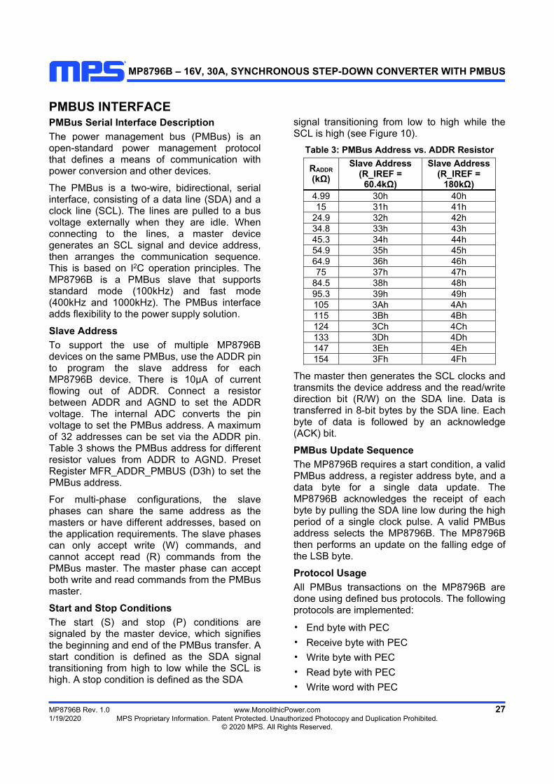
Table 3: PMBus Address vs. ADDR Resistor
RADDR (kΩ)
Slave Address (R_IREF =
60.4kΩ)
Slave Address(R_IREF =
180kΩ) 4.99 30h 40h 15 31h 41h
24.9 32h 42h 34.8 33h 43h 45.3 34h 44h 54.9 35h 45h 64.9 36h 46h 75 37h 47h
84.5 38h 48h 95.3 39h 49h 105 3Ah 4Ah 115 3Bh 4Bh 124 3Ch 4Ch 133 3Dh 4Dh 147 3Eh 4Eh 154 3Fh 4Fh
The master then generates the SCL clocks and transmits the device address and the read/write direction bit (R/W) on the SDA line. Data is transferred in 8-bit bytes by the SDA line. Each byte of data is followed by an acknowledge (ACK) bit.
PMBus Update Sequence
The MP8796B requires a start condition, a valid PMBus address, a register address byte, and a data byte for a single data update. The MP8796B acknowledges the receipt of each byte by pulling the SDA line low during the high period of a single clock pulse. A valid PMBus address selects the MP8796B. The MP8796B then performs an update on the falling edge of the LSB byte.
Protocol Usage
All PMBus transactions on the MP8796B are done using defined bus protocols. The following protocols are implemented:
• End byte with PEC
• Receive byte with PEC
• Write byte with PEC
• Read byte with PEC
• Write word with PEC

MP8796B – 16V, 30A, SYNCHRONOUS STEP-DOWN CONVERTER WITH PMBUS
MP8796B Rev. 1.0 www.MonolithicPower.com 28 1/19/2020 MPS Proprietary Information. Patent Protected. Unauthorized Photocopy and Duplication Prohibited. © 2020 MPS. All Rights Reserved.
• Read word with PEC
• Block read with PEC
PMBus Bus Message Format
In Figure 11 on page 29, unshaded cells indicate that the bus host is actively driving the bus, and shaded cells indicate that the MP8796B is driving the bus.
S = Start condition Sr = Repeated start condition P = Stop condition R = Read bit
W = Write bit A = Acknowledge bit (0)
A = Acknowledge bit (1)
“A” represents the acknowledge (ACK) bit. The ACK bit is active low (logic 0) if the transmitted byte is received successfully by a device. However, when the receiving device is the bus master, the acknowledge bit for the last byte
read is logic 1, indicated by A (see Figure 10).
Packet Error Checking (PEC)
The MP8796B PMBus interface supports the use of a packet error checking (PEC) byte. The PEC byte is transmitted by the MP8796B during a read transaction or sent by the bus host to the MP8796B during a write transaction.
The PEC byte is used by the bus host or the MP8796B to detect errors during a bus transaction (depending on whether the transaction is a read or a write). If the host determines that the PEC byte read during a read transaction is incorrect, it can decide to repeat the read if necessary. If the MP8796B
determines that the PEC byte sent during a write transaction is incorrect, it ignores the command (does not execute it) and sets a status flag. Within a group command, the host can choose to send or not send a PEC byte as part of the message to the MP8796B.
PMBus Alert Response Address (ARA)
The PMBus alert response address (ARA) is a special address that can be used by the bus host to locate any devices that need to talk to it. A host typically uses a hardware interrupt pin to monitor the PMBus ALERT pins of a number of devices. When a host interruption occurs, the host issues a message on the bus using the PMBus receive byte, or the receive byte with PEC protocol.
The special address used by the host is 0x0C. Any devices that have a PMBus use the ALERT signal to return their own 7-bit address as the 7 MSBs of the data byte. The LSB value is not used, and can be either 1 or 0. The host reads the device address from the received data byte and proceeds to handle the alert condition.
More than one device may have an active PMBus ALERT signal and attempt to communicate with the host. In this case, the device with the lowest address dominates the bus and succeeds in transmitting its address to the host. The device that succeeds disables its PMBus alert signal. If the host sees that the PMBus alert signal is still low, it continues to read addresses until all devices that need to talk to it have successfully transmitted their addresses.
Figure 10: Data Transfer over PMBus

MP8796B – 16V, 30A, SYNCHRONOUS STEP-DOWN CONVERTER WITH PMBUS
MP8796B Rev. 1.0 www.MonolithicPower.com 29 1/19/2020 MPS Proprietary Information. Patent Protected. Unauthorized Photocopy and Duplication Prohibited. © 2020 MPS. All Rights Reserved.
1. Send Byte and Send Byte with PEC 1 7 1 1 8 1 1S Slave Address Wr A Data Byte A P
1 7 1 1 8 1 8 1 1S Slave Address Wr A Data Byte A PEC A P
2. Receive Byte and Receive Byte with PEC 1 7 1 1 8 1 1S Slave Address Rd A Data Byte A P
1 7 1 1 8 1 8 1 1S Slave Address Rd A Data Byte A PEC A P
3. Write Byte and Write Byte with PEC 1 7 1 1 8 1 8 1 1S Slave Address Wr A Command Code A Data Byte A P
1 7 1 1 8 1 8 1 8 1 1 S Slave Address Wr A Command Code A Data Byte A PEC A P
4. Write Word and Write Word with PEC 1 7 1 1 8 1 8 1 8 1 1 S Slave Address Wr A Command Code A Data Byte Low A Data Byte High A P
1 7 1 1 8 1 8 1 8 1 8 1 1S Slave Address Wr A Command Code A Data Byte Low A Data Byte High A PEC A P
5. Read Byte and Read Byte with PEC 1 7 1 1 8 1 1 7 1 1 8 1 1
S Slave Address Wr A Command Code A S Slave Address Rd A Data Byte A P
1 7 1 1 8 1 1 7 1 1 8 1 8 1 1
S Slave Address Wr A Command Code A S Slave Address Rd A Data Byte A PEC A P
6. Read Word and Read Word with PEC 1 7 1 1 8 1 1 7 1 1 8 1 S Slave Address Wr A Command Code A S Slave Address Rd A Data Byte Low A
8 1 1
Data Byte High A P
1 7 1 1 8 1 1 7 1 1 8 1 S Slave Address Wr A Command Code A S Slave Address Rd A Data Byte Low A
8 1 8 1 1
Data Byte High A PEC A P
7. Block Read with PEC
Figure 11: PMBus Message Format

MP8796B – 16V, 30A, SYNCHRONOUS STEP-DOWN CONVERTER WITH PMBUS
MP8796B Rev. 1.0 www.MonolithicPower.com 30 1/19/2020 MPS Proprietary Information. Patent Protected. Unauthorized Photocopy and Duplication Prohibited. © 2020 MPS. All Rights Reserved.
Data and Numerical Formats
The MP8796B uses a direct format internally to represent real-world values such as voltage, current, power, and temperature.
All numbers without a suffix in this document are decimals unless explicitly designated otherwise.
Numbers in the binary format are indicated by the prefix “n’b”, where n is the binary count. For example, 5’b01010 indicates a 5-bit binary data, and the data is 01010.
The suffix “h” indicates a hexadecimal format, which is used for the register address numbers in this document.
The symbol “0x” indicates a hexadecimal format, which is used for the value in the register. For example, 0xA3 is a 1-byte number whose hexadecimal value is A3.
PMBus Communication Failure
A data transmission fault occurs when the data is not transferred between the devices properly. There are several types of data transmission faults listed below:
Sending too little data
Reading too little data
Sending too many bytes
Reading too many bytes
Improperly set read bit in the address byte
Unsupported command code
PMBus Reporting and Status Monitoring
The MP8796B supports real-time monitoring for some operation parameters and status with the PMBus interface (see Table 4).
Table 4: PMBus Monitored Parameters and Status
Parameter/Status PMBus Output voltage 1.25mV/LSB Output current 60.5mA/LSB Temperature 1°C/LSB Input voltage 25mV/LSB
VIN OV VIN UV
VIN OV Warn VIN UV Warn
VO OV VO UV
Over-Temperature (OT) OT Warn VO OC
VO OC Warn
Multi-Time Programming (MTP)
The MP8796B has built-in multiple-time programming (MTP) cells to store user configurations. The standard command of 15h (STORE_USER_ALL) is not currently supported in the MP8796B. Alternatively, the MTP cells can be programmed through the following command combination:
E7h (2000h) E7h (1000h) E7h (4000h)
In the MPS GUI for the MP8796B, the above commands are integrated together and named as 15h (STORE_USER_ALL). MPS’s GUI software supports the 15h command.
When MTP is being programmed, the VCC voltage may rise as high as 5V. Take caution if VCC is connected to circuits that cannot take such high voltage. The MTP programming typically takes about 300ms.

MP8796B – 16V, 30A, SYNCHRONOUS STEP-DOWN CONVERTER WITH PMBUS
MP8796B Rev. 1.0 www.MonolithicPower.com 31 1/19/2020 MPS Proprietary Information. Patent Protected. Unauthorized Photocopy and Duplication Prohibited. © 2020 MPS. All Rights Reserved.
REGISTER MAP Name Code Type Bytes Default Value MTP?OPERATION 01h R/W w/ PEC 1 0x80 Yes ON_OFF_CONFIG 02h R/W w/ PEC 1 0x16 Yes
CLEAR_FAULTS 03h Send byte w/ PEC
0 -
WRITE_PROTECT 10h R/W w/ PEC 1 0x00 Yes
STORE_USER_ALL 15h Send byte w/ PEC
0 -
RESTORE_USER_ALL 16h Send byte w/ PEC
0 -
CAPABILITY 19h R w/ PEC 1 0xB0 VOUT_MODE 20h R w/ PEC 1 0x40 VOUT_COMMAND 21h R/W w/ PEC 2 0x01CC (0.92V) Yes VOUT_MAX 24h R/W w/ PEC 2 0x0226 (1.1V) Yes VOUT_MARGIN_HIGH 25h R/W w/ PEC 2 0x0226 (1.1V) Yes VOUT_MARGIN_LOW 26h R/W w/ PEC 2 0x0190 (0.8V) Yes VOUT_SCALE_LOOP 29h R/W w/ PEC 2 0x028C (0.652) Yes VOUT_MIN 2Bh R/W w/ PEC 2 0x0170F (0.736V) Yes VIN_ON 35h R/W w/ PEC 2 0x0C (3V) Yes VIN_OFF 36h R/W w/ PEC 2 0x0B (2.75V) Yes OT_FAULT_LIMIT 4Fh R/W w/ PEC 2 0x0091(145°C) Yes OT_WARN_LIMIT 51h R/W w/ PEC 2 0x008C (140°C) Yes VIN_OV_FAULT_LIMIT 55h R/W w/ PEC 2 0x0020 (16V) Yes VIN_OV_WARN_LIMIT 57h R/W w/ PEC 2 0x001E (15V) Yes VIN_UV_WARN_LIMIT 58h R/W w/ PEC 2 0x0028 (10V) Yes TON_DELAY 60h R/W w/ PEC 2 0x0000 (0ms) Yes TON_RISE 61h R/W w/ PEC 2 0x0001 (2ms) Yes TOFF_DELAY 64h R/W w/ PEC 2 0x0000 (0ms) Yes STATUS_BYTE 78h R w/ PEC 1 STATUS_WORD 79h R w/ PEC 2 STATUS_VOUT 7Ah R w/ PEC 1 STATUS_IOUT 7Bh R w/ PEC 1 STATUS_INPUT 7Ch R w/ PEC 1 STATUS_TEMPERATURE 7Dh R w/ PEC 1 STATUS_CML 7Eh R w/ PEC 1 READ_VIN 88h R w/ PEC 2 READ_VOUT 8Bh R w/ PEC 2 READ_IOUT 8Ch R w/ PEC 2 READ_TEMPERATURE_1 8Dh R w/ PEC 2 PMBUS_REVISION 98h R w/ PEC 1 0x33h, ASCII “13” (PMBus 1.3)
MFR_ID(8) 99h Block read w/ PEC
1 (byte) + 3 (data)
0x4D 0x50 0x53, ASCII “MPS”
MFR_CTRL_COMP D0h R/W w/ PEC 1 0x09 Yes MFR_CTRL_VOUT D1h R/W w/ PEC 1 0x40 Yes MFR_CTRL_OPS D2h R/W w/ PEC 1 0x05 Yes MFR_ADDR_PMBUS D3h R/W w/ PEC 1 0xB0 Yes MFR_VOUT_OVP_FAULT_LIMIT D4h R/W w/ PEC 1 0x0E Yes MFR_OVP_NOCP_SET D5h R/W w/ PEC 1 0x00 Yes MFR_OT_OC_SET D6h R/W w/ PEC 1 0x00 Yes MFR_OC_PHASE_LIMIT D7h R/W w/ PEC 1 0x15 (31.5A) Yes MFR_HICCUP_ITV_SET D8h R/W w/ PEC 1 0x00 Yes MFR_UVP_PGOOD_ON _LIMIT D9h R/W w/ PEC 1 0x09 Yes MFR_VOUT_STEP DAh R/W w/ PEC 1 0x04 Yes MFR_LOW_POWER E5h R/W w/ PEC 1 0x00 Yes MFR_CTRL EAh R/W w/ PEC 2 bit[9] = 0, bit[3] = 0 Yes
Note:
8) For manufacturer use only.

MP8796B – 16V, 30A, SYNCHRONOUS STEP-DOWN CONVERTER WITH PMBUS
MP8796B Rev. 1.0 www.MonolithicPower.com 32 1/19/2020 MPS Proprietary Information. Patent Protected. Unauthorized Photocopy and Duplication Prohibited. © 2020 MPS. All Rights Reserved.
OPERATION (01h) OPERATION is a paged register. The OPERATION command turns the converter output on or off in conjunction with the input from the CTRL pin. OPERATION also sets the output voltage to the upper or lower margin voltages. The unit remains in the commanded operating mode until a subsequent OPERATION command or a change in the state of the CTRL pin instructs the converter to change to another mode. This OPERATION command re-enables the converter after a fault-triggered shutdown. Writing an off command followed by an on command clears all faults. Writing only an on command after a fault-triggered shutdown will not clear the fault registers.
Command OPERATION Format Unsigned binary Bit 7 6 5 4 3 2 1 0 Access R/W R/W R/W R/W R/W R/W R R Function X X Default Value 1 0 0 0 0 0 X X
Bit[7:6] Bit[5:4] Bit[3:2] Bit[1:0] On/Off Margin state 01h
00 XX XX XX Immediate off N/A 0x00 01 XX XX XX Soft off N/A 0x40 10 00 XX XX On Off 0x80 10 01 01 XX On Margin low (ignore fault) 0x94 10 01 10 XX On Margin low (act on fault) 0x98 10 10 01 XX On Margin high (ignore fault) 0xA4 10 10 10 XX On Margin high (act on fault) 0xA8
ON_OFF_CONFIG (02h)
The ON_OFF_CONFIG command configures the combination of the CTRL input and the PMBus commands to turn the converter on and off. This includes how the converter responds when an input voltage is applied.
Command ON_OFF_CONFIG Format Unsigned binary Bit 7 6 5 4 3 2 1 0 Access R R R R/W R/W R/W R/W R Function X On Op Ctrl Pol_Ctrl Delay Default Value 0 0 0 1 0 1 1 0
On
The on bit sets the device to either operate whenever the input voltage is present, or for the on/off function to be controlled by the CTRL and PMBus commands.
Bit[4] Value Meaning
0 Converter powers up when the input voltage is present, regardless of state the of the CTRL pin.
1 Converter does not power up until commanded by the CTRL pin and OPERATION command (as programmed in bit[3:0]).
Op
The op bit controls how the converter responds to the OPERATION commands.
Bit[3] Value Meaning
0 Converter ignores the “on” bit in the OPERATION command from the PMBus.
1 Converter responds to the “on” bit in the OPERATION command from the PMBus.

MP8796B – 16V, 30A, SYNCHRONOUS STEP-DOWN CONVERTER WITH PMBUS
MP8796B Rev. 1.0 www.MonolithicPower.com 33 1/19/2020 MPS Proprietary Information. Patent Protected. Unauthorized Photocopy and Duplication Prohibited. © 2020 MPS. All Rights Reserved.
Ctrl
The ctrl bit controls how the converter responds to the CTRL pin.
Bit[2] Value Meaning
0 Converter ignores the CTRL pin (on/off function is controlled by the OPERATION command).
1 Converter requires the CTRL pin to be asserted to power up. Depending on the bit[3] op bit, the OPERATION command may also be required to instruct the converter to power up.
Pol_ctrl
The pol_ctrl bit sets the polarity of the CTRL pin.
Bit[1] Value Meaning
0 Active low (pull the CTRL pin low to start the converter).
1 Active high (pull the CTRL pin high to start the converter).
Delay
The delay bit sets the turn-off action when the converter is commanded to turn off through the PMBus. This bit is read-only and cannot be modified by the end user.
Bit[0] Value Meaning
0 TOFF_DELAY, TOFF_FALL
CLEAR_FAULTS (03h)
The CLEAR_FAULTS command resets all stored warning and fault flags. If a fault or warning condition still remains when the CLEAR_FAULTS command is issued, the ALT# signal may not be cleared or is reasserted almost immediately. Issuing a CLEAR_FAULTS command will not cause the converter to restart in the event of a fault shutdown. The converter restart must be done by issuing an OPERATION command after the fault condition is cleared. This command uses the PMBus to send the byte protocol.
WRITE_PROTECT (10h)
The WRITE_PROTECT command controls writes to the converter. This command provides protection against accidental changes. This command is not intended to provide protection against deliberate changes to the converter’s configuration or operation.
All the supported commands may have their parameters read, regardless of the WRITE_PROTECT settings.
Bit[7:0] Value Meaning
0 0 0 0 0 0 0 0 Enable writes to all commands.
0 0 1 0 0 0 0 0 Disable all writes except to the WRITE_PROTECT, OPERATION, PAGE, ON_OFF_ CONFIG, and VOUT_COMMAND commands.
0 1 0 0 0 0 0 0 Disable all writes except to the WRITE_PROTECT, OPERATION, and PAGE commands.
1 0 0 0 0 0 0 0 Disable all writes except to the WRITE_PROTECT command.
When 10h is set to a value other than 0x00, in order to program the MTP, 15h must be programmed through the MPS GUI. A separate MTP command on E7h cannot be used. See the Multi-Time Programming (MTP) section on page 30 for details on MTP programming.
The default value of 10h is 0x00.
STORE_USER_ALL (15h)
This command writes all data from the registers to the internal MTPs. This process operates when the MP8796B receives a STORE_USER_ALL command from the PMBus interface. Currently, the MP8796B does not support a standard 15h command, but it can accept a 15h command from MPS’s GUI software for the MP8796B. See the Multi-Time Programming (MTP) section on page 30 for details.

MP8796B – 16V, 30A, SYNCHRONOUS STEP-DOWN CONVERTER WITH PMBUS
MP8796B Rev. 1.0 www.MonolithicPower.com 34 1/19/2020 MPS Proprietary Information. Patent Protected. Unauthorized Photocopy and Duplication Prohibited. © 2020 MPS. All Rights Reserved.
The following registers can be stored using STORE_USER_ALL.
OPERATION (01h) TOFF_DELAY (64h) ON_OFF_CONFIG (02h) MFR_REVISION (9Bh) WRITE_PROTECT (10h) MFR_4_DIGIT (9Dh) VOUT_COMMAND (21h) MFR_CTRL_COMP (D0h) VOUT_MAX (24h) MFR_CTRL_VOUT (D1h) VOUT_MARGIN_HIGH (25h) MFR_CTRL_OPS (D2h) VOUT_MARGIN_LOW (26h) MFR_ADDR_PMBUS (D3h) VOUT_SCALE_LOOP (29h) MFR_VOUT_OVP_FAULT_LIMIT (D4h) VOUT_MIN (2Bh) MFR_OVP_NOCP_SET (D5h) VIN_ON (35h) MFR_OT_OC_SET (D6h) VIN_OFF (36h) MFR_OC_PHASE_LIMIT (D7h) OT_FAULT_LIMIT (4Fh) MFR_HICCUP_ITV_SET (D8h) OT_WARN_LIMIT (51h) MFR_UVP_PGOOD_ON_LIMIT (D9h) VIN_OV_FAULT_LIMIT (55h) MFR_VOUT_STEP (DAh) VIN_OV_WARN_LIMIT (57h) MFR_LOW_POWER (E5h) VIN_UV_WARN_LIMIT (58h) MFR_CTRL (EAh) TON_DELAY (60h) MFR_LOW_POWER (E5h) TON_RISE (61h) MFR_CTRL (EAh)
RESTORE_USER_ALL (16h)
The RESTORE_USER_ALL command instructs the MP8796B to copy the entire contents of the MTP values to the matching locations in the registers. The values in the registers are overwritten by the value retrieved from the MTP. Any items in the MTPs that do not have matching locations in the operating memory are ignored.
The RESTORE_USER_ALL command can be used while the MP8796B is operating. However, this is not recommended as the MP8796B may be unresponsive during the operation with unpredictable results.
This command is write-only.
CAPABILITY (19h)
The CAPABILITY command returns information about the PMBus functions supported by the MP8796B. This command is read with the PMBus read byte protocol.
Command CAPABILITY Format Unsigned binary Bit 7 6 5 4 3 2 1 0 Access R R R R R R R R Function PEC Max bus speed Alert X X X X Default Value 1 0 1 1 0 0 0 0 PEC supported, max speed 1MHz, supports PMBus alert and ARA.
Bit[6:5] Value Meaning
0 0 Maximum supported bus speed is 100kHz.
0 1 Maximum supported bus speed is 1MHz.
1 0 Maximum supported bus speed is 400kHz.
1 1 Reserved.
The default value of 19h is 0xB0.

MP8796B – 16V, 30A, SYNCHRONOUS STEP-DOWN CONVERTER WITH PMBUS
MP8796B Rev. 1.0 www.MonolithicPower.com 35 1/19/2020 MPS Proprietary Information. Patent Protected. Unauthorized Photocopy and Duplication Prohibited. © 2020 MPS. All Rights Reserved.
VOUT_MODE (20h)
The VOUT_MODE command reads and sets the output voltage. The 3 MSBs are used to determine the data format (only direct format is supported in the MP8796B), and the other 5 bits represent the exponent used in the output voltage read/write commands.
The default value of 20h is 0x40.
VOUT_COMMAND (21h)
VOUT_COMMAND sets the output voltage of the MP8796B. Together, VOUT_COMMAND and VOUT_SCALE_ LOOP determine the feedback reference voltage: VOUT_COMMAND x VOUT_SCALE_LOOP.
See the Output Voltage Setting section on page 22 for details on setting the output voltage.
Command VOUT_COMMAND Format Direct Bit 15 14 13 12 11 10 9 8 7 6 5 4 3 2 1 0 Access R R R R R/W R/W R/W R/W R/W R/W R/W R/W R/W R/W R/W R/WFunction X 2mV/LSB Default Value 0 0 0 0 0 0 0 1 1 1 0 0 1 1 0 0
The value is unsigned, and 1LSB = 2mV. The default value of 21h is 0.92V, which is 0x01CC.
VOUT_MAX (24h)
The VOUT_MAX command sets an upper limit on the output voltage of the converter to enable the command, regardless of any other commands or combinations. The intent of this command is to provide a safeguard against an accidental setting of the output voltage to a possibly destructive level, not to be the primary output over-voltage protection.
Command VOUT_MAX Format Direct Bit 15 14 13 12 11 10 9 8 7 6 5 4 3 2 1 0 Access R R R R R/W R/W R/W R/W R/W R/W R/W R/W R/W R/W R/W R/WFunction x 2mV/LSB Default Value 0 0 0 0 0 0 1 0 0 0 1 0 0 1 1 0
If an attempt is made to program the output voltage above the limit set by this command, the device responds as follows:
The commanded output voltage is set to VOUT_MAX
The VOUT bit is set in STATUS_WORD
The VOUT_MAX_MIN warning bit is set in the STATUS_VOUT register
The device notifies the host
The value is unsigned, and 1LSB = 2mV. The maximum value of VOUT_MAX is 5.5V, and the default value is 1.1V. Therefore, the default value of 24h is 0x0226.
VOUT_MARGIN_HIGH (25h)
The value is unsigned, and 1LSB = 2mV. The default value is 1.1V. Therefore, the default value of 25h is 0x0226.
Command VOUT_MARGIN_HIGH Format Direct Bit 15 14 13 12 11 10 9 8 7 6 5 4 3 2 1 0 Access R R R R R/W R/W R/W R/W R/W R/W R/W R/W R/W R/W R/W R/WFunction X X X X 2mV/LSB Default Value 0 0 0 0 0 0 1 0 0 0 1 0 0 1 1 0

MP8796B – 16V, 30A, SYNCHRONOUS STEP-DOWN CONVERTER WITH PMBUS
MP8796B Rev. 1.0 www.MonolithicPower.com 36 1/19/2020 MPS Proprietary Information. Patent Protected. Unauthorized Photocopy and Duplication Prohibited. © 2020 MPS. All Rights Reserved.
VOUT_MARGIN_LOW (26h) Command VOUT_MARGIN_LOW Format Direct Bit 15 14 13 12 11 10 9 8 7 6 5 4 3 2 1 0 Access R R R R R/W R/W R/W R/W R/W R/W R/W R/W R/W R/W R/W R/WFunction X 2mV/LSB Default Value 0 0 0 0 0 0 0 1 1 0 0 1 0 0 0 0
The value is unsigned, and 1LSB = 2mV. The default value is 0.8V, which is 0x0190.
VOUT_SCALE_LOOP (29h)
VOUT_SCALE_LOOP sets the feedback resistor divider ratio, and is equal to VFB / VOUT. Regardless of whether an external or internal feedback resistor divider is used, VOUT_SCALE_LOOP should match the actual feedback resistor divider value.
Command VOUT_SCALE_LOOP Format Direct Bit 15 14 13 12 11 10 9 8 7 6 5 4 3 2 1 0 Access R R R R R/W R/W R/W R/W R/W R/W R/W R/W R/W R/W R/W R/WFunction X 0.001/LSB Default Value 0 0 0 0 0 0 1 0 1 0 0 0 1 1 0 0
The value is unsigned, and 1LSB = 0.001. The default value is 0.652, which is 0x028C.
VOUT_MIN (2Bh)
The VOUT_MIN command sets a lower limit on the output voltage of the converter to enable a command, regardless of any other commands or combinations. The intent of this command is to provide a safeguard against an accidental setting of the output voltage to a possible destructive level, not to be the primary output under-voltage protection.
Command VOUT_MIN Format Direct Bit 15 14 13 12 11 10 9 8 7 6 5 4 3 2 1 0 Access R R R R R/W R/W R/W R/W R/W R/W R/W R/W R/W R/W R/W R/WFunction X 2mV/LSB Default Value 0 0 0 0 0 0 0 1 0 1 1 1 0 0 0 0
If an attempt is made to program the output voltage below the limit set by this command, the device responds as follows:
The commanded output voltage is set to VOUT_MIN
The VOUT bit is set in STATUS_WORD
The VOUT_MAX_MIN warning bit is set in the STATUS_VOUT register
The device notifies the host
The minimum value of VOUT_MIN is 0.5V. The value is unsigned, and 1LSB = 2mV. The default value is 0.736V, which is 0x0170.
VIN_ON (35h)
The VIN_ON command sets the value of the input voltage (in V) at which the converter should start up if all other required start-up conditions are met. The VIN_ON value can be set between 4V and 15V with a 0.25V increment. The VIN_ON value should always be set above the VIN_OFF value, with enough margin so there is no bouncing between VIN_ON and VIN_OFF during power conversion.

MP8796B – 16V, 30A, SYNCHRONOUS STEP-DOWN CONVERTER WITH PMBUS
MP8796B Rev. 1.0 www.MonolithicPower.com 37 1/19/2020 MPS Proprietary Information. Patent Protected. Unauthorized Photocopy and Duplication Prohibited. © 2020 MPS. All Rights Reserved.
Command VIN_ON Format Direct Bit 15 14 13 12 11 10 9 8 7 6 5 4 3 2 1 0 Access R R R R R R R R R R R/W R/W R/W R/W R/W R/WFunction X 250mV/LSB Default Value 0 0 0 0 0 0 0 0 0 0 0 0 1 1 0 0
The value is unsigned, and 1LSB = 250mV. The default value is 3V, which is 0x000C.
VIN_OFF (36h)
The VIN_OFF command sets the value of the input voltage (in V) at which the converter should stop power conversion once operation has started. The VIN_OFF value can be set between 2.75V and 14.75V with a 0.25V increment. The VIN_OFF value should be always set below the VIN_ON value, with enough margin so that there is no bouncing between VIN_OFF and VIN_ON during power conversion.
Command VIN_OFF Format Direct Bit 15 14 13 12 11 10 9 8 7 6 5 4 3 2 1 0 Access R R R R R R R R R R R/W R/W R/W R/W R/W R/WFunction X 250mV/LSB Default Value 0 0 0 0 0 0 0 0 0 0 0 0 1 0 1 1
The value is unsigned, and 1LSB = 250mV. The default value is 2.75V, which is 0x000B. OT_FAULT_LIMIT (4Fh)
The OT_FAULT_LIMIT configures or reads the threshold for over-temperature (OT) fault detection. If the measured temperature exceeds this value, an OT fault is triggered, the OT fault flags are set in the STATUS BYTE (78h) and STATUS_WORD (79h), respectively, and the ALT# signal is asserted. After the measured temperature falls below the value in this register, the MOSFET may be switched back on with the OPERATION command when the part works in latch-off mode. The minimum temperature fault detection time should be shorter than 20ms. The temperature ranges from 0°C to +255°C.
If an OT fault occurs when the temperature exceeds this register value, the part implements auto-retry when the temperature drops below 20°C of this register value.
Command OT_FAULT_LIMIT Format Direct Bit 15 14 13 12 11 10 9 8 7 6 5 4 3 2 1 0 Access R R R R R R R R R/
W R/W
R/W
R/W
R/W
R/W
R/W
R/W
Function X 1°C/LSB Default Value
0 0 0 0 0 0 0 0 1 0 0 1 0 0 0 1
The value is unsigned, and 1LSB = 1°C. The default value is 0091h. The corresponding value is 145°C.
The OT_FAULT_LIMIT setting value should be below 160°C. If the OT_FAULT_LIMIT value is above 160oC, the register value is neglected, and the MP8796B enters thermal shutdown when the junction temperature reaches 160°C.
Table 5 shows the relationship between direct values and real-world values.
Table 5: Direct Value vs. Real-World Value
Direct Value Real-World Value (°C) 0000 0000 0 0000 0001 +1 1111 1111 +255

MP8796B – 16V, 30A, SYNCHRONOUS STEP-DOWN CONVERTER WITH PMBUS
MP8796B Rev. 1.0 www.MonolithicPower.com 38 1/19/2020 MPS Proprietary Information. Patent Protected. Unauthorized Photocopy and Duplication Prohibited. © 2020 MPS. All Rights Reserved.
OT_WARN_LIMIT (51h)
OT_WARN_LIMIT configures or reads the threshold for over-temperature (OT) warning detection. If the sensed temperature exceeds this value, an OT warning is triggered, the OT warning flags are set in STATUS BYTE (78h) and STATUS_WORD (79h), respectively, and the ALT# signal is asserted. The minimum temperature warning detection time should be shorter than 20ms.
Command OT_WARN_LIMIT Format Direct Bit 15 14 13 12 11 10 9 8 7 6 5 4 3 2 1 0 Access
R R R R R R R R R/W
R/W
R/W
R/W
R/W
R/W
R/W
R/W
Function X 1°C/LSB Default Value
0 0 0 0 0 0 0 0 1 0 0 0 1 1 0 0
The value is unsigned, and 1LSB = 1°C. The default value is 0x008Ch. The corresponding value is 140°C. The OT_WARN_LIMIT setting value should be below 160°C. The relationship between the direct value and real-world value is the same as it is with the command OT_FAULT_LIMIT.
VIN_OV_FAULT_LIMIT (55h)
The VIN_OV_FAULT_LIMIT command configures or reads the threshold for input over-voltage (OV) fault detection. If the measured value of VIN exceeds the value in this register, the VIN OV fault flags are set in their respective registers. The MP8796B disables the power stage. When VIN drops below the VIN_OV_FAULT_LIMIT, the MP8796B begins working again.
Command VIN_OV_FAULT_LIMIT Format Direct Bit 15 14 13 12 11 10 9 8 7 6 5 4 3 2 1 0 Access R R R R R R R R R R R/W R/W R/W R/W R/W R/WFunction X 500mV/LSB Default Value
0 0 0 0 0 0 0 0 0 0 1 0 0 0 0 0
The value is unsigned and 1LSB = 500mV. The default value is 20h. The corresponding value is 16V. The VIN_OV_FAULT_LIMIT setting value should not exceed 18V.
VIN_OV_WARN_LIMIT (57h)
The VIN_OV_WARN_LIMIT command configures or reads the threshold for input over-voltage (OV) warning detection. If the measured value of VIN exceeds the value in this register, the VIN OV warning flags are set in their respective registers, and the ALT# signal is asserted.
Command VIN_OV_WARN_LIMIT Format Direct Bit 15 14 13 12 11 10 9 8 7 6 5 4 3 2 1 0 Access R R R R R R R R R R R/W R/W R/W R/W R/W R/WFunction X 500mV/LSB Default Value
0 0 0 0 0 0 0 0 0 0 0 1 1 1 1 0
The value is unsigned and 1LSB = 500mV. The default value is 0x1E. The corresponding value is 15V. The VIN_OV_WARN_LIMIT setting value should not exceed 18V.

MP8796B – 16V, 30A, SYNCHRONOUS STEP-DOWN CONVERTER WITH PMBUS
MP8796B Rev. 1.0 www.MonolithicPower.com 39 1/19/2020 MPS Proprietary Information. Patent Protected. Unauthorized Photocopy and Duplication Prohibited. © 2020 MPS. All Rights Reserved.
VIN_UV_WARN_LIMIT (58h)
The VIN_UV_WARN_LIMIT command configures or reads the threshold for input under-voltage (UV) fault detection. If the measured value of VIN falls below the value in this register, the VIN UV warning flags are set in their respective registers, and the ALT# signal is asserted.
Command VIN_UV_WARN_LIMIT Format Direct Bit 15 14 13 12 11 10 9 8 7 6 5 4 3 2 1 0 Access R R R R R R R R R R R/W R/W R/W R/W R/W R/WFunction X 250mV/LSB Default Value
0 0 0 0 0 0 0 0 0 0 1 0 1 0 0 0
The value is unsigned and 1LSB = 250mV. The default value is 0x28. The corresponding value is 10V. The VIN_UV_WARN_LIMIT setting value should not be set below 3.3V.
TON_DELAY (60h)
The TON_DELAY command sets the time (in ms) from when a start condition is received (as programmed by the ON_OFF_CONFIG command) until the output voltage starts to rise.
Command TON_DELAY Format Direct Bit 15 14 13 12 11 10 9 8 7 6 5 4 3 2 1 0 Access R R R R R R/W R/W R/W R/W R/W R/W R/W R/W R/W R/W R/WFunction X 4ms/LSB Default Value
0 0 0 0 0 0 0 0 0 0 0 0 0 0 0 0
The value is unsigned and 1LSB = 4ms. The maximum value is FFh (1020ms). The default value is 0ms.
TON_RISE (61h)
The TON_RISE command sets the soft-start time (in ms) from when the output starts to rise until the voltage reaches the regulation point.
Command TON_RISE Format Direct Bit 15 14 13 12 11 10 9 8 7 6 5 4 3 2 1 0 Access R R R R R/W R/W R/W R/W R/W R/W R/W R/W R/W R/W R/W R/WFunction X 1ms/LSB Default Value
0 0 0 0 0 0 0 0 0 0 0 0 0 0 0 1
The only supported values are:
3’b000: 1ms 3’b001: 2ms 3’b010: 4ms 3’b011: 8ms 3’b100 and up: 16ms
The default value is 0x01 (i.e. 2ms for soft-start time).

MP8796B – 16V, 30A, SYNCHRONOUS STEP-DOWN CONVERTER WITH PMBUS
MP8796B Rev. 1.0 www.MonolithicPower.com 40 1/19/2020 MPS Proprietary Information. Patent Protected. Unauthorized Photocopy and Duplication Prohibited. © 2020 MPS. All Rights Reserved.
TOFF_DELAY (64h)
The TOFF_DELAY command sets the time in ms from EN off to the moment when the output starts to fall.
command TOFF_DELAY
format Direct
Bit 15 14 13 12 11 10 9 8 7 6 5 4 3 2 1 0
Access r r r r r r r r r/w r/w r/w r/w r/w r/w r/w r/w
Function x 4ms/LSB
Default value 0 0 0 0 0 0 0 0 0 0 0 0 0 0 1 0
The value is unsigned and 1LSB=4ms. The maximum value is FFh (1020ms). The default value is 0ms.
STATUS_BYTE (78h)
The STATUS_BYTE command returns the value of a number of flags indicating the state of the MP8796B. Accesses to this command should use the read byte protocol. To clear bits in this register, the underlying fault should be removed and a CLEAR_FAULTS command should be issued.
Bits Name Behavior Default Description
[7] RESERVED 0 Always read as 0.
[6] OFF Live 0 0: Part enabled 1: Part disabled. This can be due to an VIN UV/OV fault, or the OPERATION command turning off
[5] VOUT_OV 0 An output over-voltage fault has occurred.
[4] IOUT_OC_FAULT Latched 0 0: No over-current fault detected 1: Over-current fault detected
[3] VIN_UV 0 Not supported, always read as 0.
[2] OT_FAULT_WARN Live 0 0: No over-temperature warning or fault detected 1: Over-temperature warning or fault detected
[1] COMM_ERROR Latched 0 0: No communication error detected 1: Communication error detected
[0] NONE_OF_THE_ABOVE Live 0 0: No other fault or warning 1: Fault or warning not listed in bit[7:1] has occurred
STATUS_WORD (79h)
The STATUS_WORD returns the value of a number of flags indicating the state of the MP8796B. To clear bits in this register, the underlying fault should be removed and a CLEAR_FAULTS command should be issued.
Bits Name Behavior Default Description
[15] VOUT_STATUS Live 0 0: No output fault or warning 1: Output fault or warning
[14] IOUT_STATUS Live 0 0: No IOUT fault 1: IOUT fault
[13] VIN_STATUS Live 0
0: No VIN fault 1: VIN fault, at the period when VIN starts up, the initial flag is 1 before VIN passes the UVLO threshold. The flag is cleared once VIN passes the UVLO threshold
[12] MFR_STATUS 0 Always read as 0.
[11] POWER_GOOD# Live 0 0: Power good signal is asserted 1: Power good signal is not asserted

MP8796B – 16V, 30A, SYNC STEP-DOWN CONVERTER WITH PMBUSTM
MP8796B Rev 1.0 www.MonolithicPower.com 41 1/19/2020 MPS Proprietary Information. Patent Protected. Unauthorized Photocopy and Duplication Prohibited. © 2020 MPS. All Rights Reserved.
[10] RESERVED 0 Always read as 0.
[9] RESERVED 0 Always read as 0.
[8] UNKNOWN Latched 0 0: No other fault has occurred 1: A fault type not specified in bit[15:1] of STATUS_ WORD has been detected.
Low Byte
STATUS_BYTE STATUS BYTE is the low byte of STATUS WORD.
STATUS_VOUT (7Ah)
The STATUS_VOUT command returns one data byte with contents as follows.
Bits Name Behavior Default Description
[7] VOUT_OV_FAULT Live 0 0: No output OV fault 1: Output OV fault
[6] RESERVED Latched 0 Always read as 0.
[5] RESERVED Latched 0 Always read as 0.
[4] VOUT_UV_FAULT Live 0 0: No output UV fault 1: Output UV fault
[3] VOUT_MAX_MIN Live 0
0: No VOUT_MAX, VOUT_MIN warning 1: An attempt has been made to set the output voltage to a value above that allowed by the VOUT_MAX command or below the limit allowed by the VOUT_MIN command
[2] RESERVED 0 Always read as 0.
[1] RESERVED 0 Always read as 0.
[0] UNKNOWN Latched 0 0: No other fault has occurred 1: A fault type not specified in bit[15:1] of STATUS_ WORD has been detected
STATUS_IOUT (7Bh) Command STATUS_IOUT Format Unsigned binary Bit 7 6 5 4 3 2 1 0 Access R R R R R R R R Function IOUT_OC IOUT_OC & VOUT_UV IOUT_OC_WARNING X X X X X Default Value 0 0 0 0 0 0 0 0
STATUS_INPUT (7Ch)
The STATUS_INPUT returns the value of the flags indicating the input voltage status of the MP8796B. To clear the bits in this register, the underlying fault or warning should be removed and a CLEAR_FAULTS command should be issued.
Bits Name Behavior Default Set Description
[7] VIN_OV_FAULT R, latched 0 0: No over-voltage detected on the OV pin 1: Over-voltage detected on the OV pin
[6] VIN_OV_WARN R, latched 0 0: No over-voltage condition on VIN 1: Over-voltage condition on VIN has occurred
[5] VIN_UV_WARN R, latched 0 0: No under-voltage condition on VIN 1: Under-voltage condition on VIN has occurred
[4:0] RESERVED R 0 Always read as 0000.

MP8796B – 16V, 30A, SYNCHRONOUS STEP-DOWN CONVERTER WITH PMBUS
MP8796B Rev. 1.0 www.MonolithicPower.com 42 1/19/2020 MPS Proprietary Information. Patent Protected. Unauthorized Photocopy and Duplication Prohibited. © 2020 MPS. All Rights Reserved.
STATUS_TEMPERATURE (7Dh)
The STATUS_TEMPERATURE returns the value of flags indicating the over temperature fault or over temperature waring of MP8796B. To clear the bits in this register, the underlying fault should be removed and a CLEAR_FAULTS command should be issued.
Bits Name Behavior Default Description
[7] OT_FAULT R, latched 0 1: Over-temperature fault has occurred
[6] OT_WARNING R, latched 0 1: Over-temperature warning has occurred
[5:0] RESERVED R 0 Always read as 0.
STATUS_CML (7Eh) Command STATUS_CML Format Unsigned binary Bit 7 6 5 4 3 2 1 0 Access R R R R R R R R
Function Invalid or
unsupported command
Invalid or unsupported data
X Memory fault
detected X X Other fault
Memory busy
Default Value 0 0 0 0 0 0 0 0
READ_VIN (88h)
The READ_VIN command returns the 10-bit measured value of the input voltage.
Command READ_VOUT Format Direct Bit 15 14 13 12 11 10 9 8 7 6 5 4 3 2 1 0 Access R R R R R R R R R R R R R R R R Function X 25mV/LSB Default Value 0 0 0 0 0 0 0 0 0 0 0 0 0 0 0 0
READ_VOUT (8Bh)
The READ_VOUT command returns the 13-bit measured value of the output voltage.
Command READ_VOUT Format Direct Bit 15 14 13 12 11 10 9 8 7 6 5 4 3 2 1 0 Access R R R R R R R R R R R R R R R R Function X 1.25mV/LSB Default Value 0 0 0 0 0 0 0 0 0 0 0 0 0 0 0 0
READ_IOUT (8Ch)
The READ_IOUT command returns the 14-bit measured value of the output current. This value is also compared with IOUT_OC_FAULT_LIMIT and IOUT_OC_WARN_LIMIT, and can affect STATUS_IOUT.
Command READ_IOUT Format Direct Bit 15 14 13 12 11 10 9 8 7 6 5 4 3 2 1 0 Access R R R R R R R R R R R R R R R R Function X 62.5mA/LSB Default Value 0 0 0 0 0 0 1 0 0 1 0 1 1 0 0 0
MP8796B – 16V, 30A, SYNCHRONOUS STEP-DOWN CONVERTER WITH PMBUS
MP8796B Rev. 1.0 www.MonolithicPower.com 43 1/19/2020 MPS Proprietary Information. Patent Protected. Unauthorized Photocopy and Duplication Prohibited. © 2020 MPS. All Rights Reserved.
READ_TEMPERATURE_1 (8Dh)
The READ_TEMPERATURE_1 command returns the internal sensed temperature. This value is also used internally for over-temperature warning and fault detection. This data has a range of -255°C to +255°C.
Command READ_TEMPERATURE_1 Format Direct Bit 15 14 13 12 11 10 9 8 7 6 5 4 3 2 1 0 Access R R R R R R R/W R/W R/W R/W R/W R/W R/W R/W R/W R/WFunction X Sign 1°C/LSB Default Value 0 0 0 0 0 0 0 0 0 0 1 1 0 0 1 0
READ_TEMPERATURE_1 is a 2-byte, two’s complement integer. Bit[9] is the sign bit. Table 6 shows the relationship between direct values and real-world values.
Table 6: Direct Value vs. Real-World Value
Sign Direct Value Real-World Value (°C) 0 0 0000 0000 0 0 0 0000 0001 1 0 1 1111 1111 +511 1 0 0000 0001 -511 1 1 1111 1111 -1
PMBUS_REVISION (98h)
The PMBUS_REVISION command returns the protocol revision used. Accesses to this command should use the read byte protocol. Bit[7:4] indicates the PMBus revision of specification Part I to which the device is compliant. Bit[3:0] indicates the revision of specification Part II to which the device is compliant.
Name PMBUS_REVISION Format Unsigned binary Bit 7 6 5 4 3 2 1 0 Access R R R R R R R R Default Value 0 0 1 1 0 0 1 1
Bit[7:4] is always read as 4’b0011, specification PMBus Part I Revision 1.3.
Bit[3:0] is always read as 4’b0011, specification PMBus Part II Revision 1.3.
MFR_ID (99h)
The MFR_ID command returns the company identification.
Byte Byte Name Value Description
0 Byte Count 0x03 Always read as 0x03. The number of data bytes that the block read command expects to read.
1 Character 1 0x4D, ASCII of “M” Always read as 0x4D.
2 Character 2 0x50, ASCII of “P” Always read as 0x50.
3 Character 3 0x53, ASCII of “S” Always read as 0x53.

MP8796B – 16V, 30A, SYNCHRONOUS STEP-DOWN CONVERTER WITH PMBUS
MP8796B Rev. 1.0 www.MonolithicPower.com 44 1/19/2020 MPS Proprietary Information. Patent Protected. Unauthorized Photocopy and Duplication Prohibited. © 2020 MPS. All Rights Reserved.
MFR_CTRL_COMP (D0h)
The MFR_CTRL_COMP command adjusts the loop compensation of the MP8796B.
Bits Name Access Behavior Default Description
[7:5] RESERVED R/W Live 000
[4] Cff R/W Live 0
Sets the feed-forward capacitance when the internal feedback resistor divider is selected.
0: 20pF 1: 50pF
[3:1] RAMP R/W Live 100
Set the internal ramp compensation to stabilize the loop. Note: The actual ramp amplitude is related to EAh[3]. Refer to the register EAh description below for details.
EAh[3] = 0 (single-phase)
EAh[3] = 1 (multi-phase)
000: 5.6mV ramp 000: 8.6mV ramp 001: 9.8mV ramp 001: 15mV ramp 010: 18mV ramp 010: 27mV ramp 011: 30mV ramp 011: 45mV ramp 100: 8.5mV ramp 100: 13mV ramp
101: 15.1mV ramp 101: 23mV ramp 110: 27mV ramp 110: 41mV ramp 111: 44mV ramp 111: 68mV ramp
[0] Slave Fault Detection
R/W Live 1
Enables or disables the slave fault detection function through the PG pin.
0: Slave-phase fault detection is enabled 1: Slave-phase fault detection is disabled
MFR_CTRL_VOUT (D1h)
The MFR_CTRL_VOUT command adjusts the output voltage behaviors of the MP8796B.
Bits Name Access Behavior Default Description
[7] RESERVED R/W Live 0
[6] Vo discharge
R/W Live 1 1: Output voltage discharge at CTRL low 0: No active output voltage discharge
[5:2] PG delay R/W Live 0000
0000: 1ms 0001: 2ms … 1110: 15ms
1111: 0ms
[1:0] VO_RANGE R/W Live 00
Chooses the internal voltage divider ratio.
00: VREF / VO = 1, VO = 0.4V to 0.672V, LSB = 2mV 01: VREF / VO = 0.5, VO = 0.4V to 1.344V, LSB = 2mV 10: VREF / VO = 0.25, VO = 0.7V to 2.688V, LSB = 2mV 11: VREF / VO = 0.125, VO = 1.3V to 5.376V, LSB = 2mV
The default value of D1h is 0x40.

MP8796B – 16V, 30A, SYNCHRONOUS STEP-DOWN CONVERTER WITH PMBUS
MP8796B Rev. 1.0 www.MonolithicPower.com 45 1/19/2020 MPS Proprietary Information. Patent Protected. Unauthorized Photocopy and Duplication Prohibited. © 2020 MPS. All Rights Reserved.
MFR_CTRL_OPS (D2h)
The MFR_CTRL_OPS command sets the switching frequency and light-load operation mode of the MP8796B.
Bits Name Access Behavior Default Description
[7:3] RESERVED 00000
[2:1] SWITCHING_ FREQUENCY
R/W Live 10
00: Set fSW to 400kHz 01: Set fSW to 600kHz 10: Set fSW to 800kHz 11: Set fSW to 1000kHz
[0] SKIP_CCM (SYNC)
R/W Live 1 0: Pulse-skip mode at light load 1: Forced CCM at light load
The default value of D2h is 0x05.
MFR_ADDR_PMBUS (D3h) Command MFR_ADDR_PMBUS Format Direct Bit 7 6 5 4 3 2 1 0 Access R/W R/W R/W R/W R/W R/W R/W R/WFunction Enable ADDR Default Value 1 0 1 1 0 0 0 0
Bit[7] (enable bit):
1: The address is decided by MFR_ADDR_PMBUS [6:0]
0: The address is decided by the ADDR pin
The default value of D3h is 0xB0.
MFR_VOUT _OVP_FAULT_LIMIT (D4h)
This MFR_VOUT _FAULT_LIMIT command sets the thresholds for UVP and OVP.
Bits Name Access Behavior Default Description
[7:4] RESERVED 0000
[3:2] OV_EXIT_ TH
R/W Live 11
Sets the OVP exit threshold. 00: 10% of VREF 01: 50% of VREF 10: 80% of VREF 11: 102.5% of VREF
[1:0] OV_TH R/W Live 10
Sets the OVP entry threshold. 00: 115% of VREF 01: 120% of VREF 10: 125% of VREF 11: 130% of VREF
The above thresholds are relative values of the reference voltage. The default value of D4h is 0x0E.

MP8796B – 16V, 30A, SYNCHRONOUS STEP-DOWN CONVERTER WITH PMBUS
MP8796B Rev. 1.0 www.MonolithicPower.com 46 1/19/2020 MPS Proprietary Information. Patent Protected. Unauthorized Photocopy and Duplication Prohibited. © 2020 MPS. All Rights Reserved.
MFR_OVP_NOCP_SET (D5h)
This MFR_OVP_NOCP_SET command sets the responses of the output voltage OVP.
Bits Name Access Behavior Default Description
[7:4] RESERVED 0000
[3] DELAY_NOCP (D400)
R/W Live 0 0: 100ns delay after NOCP 1: 200ns delay after NOCP
[2] NOCP R/W Live 0 0: Set NOCP to -10A 1: Set NOCP to -15A
[1:0] VOUT_OV _Response
R/W Live 00
00: Latch off with output voltage discharge 01: Latch off without output voltage discharge in DCM 10: Hiccup with output voltage discharge 11: Hiccup without output voltage discharge in DCM
Bit[1:0] of the MFR_OVP_NOCP_SET command tells the converter what action to take in response to an output over-voltage fault. The device also:
Sets the VOUT_OV bit in STATUS_BYTE
Sets the VOUT bit in STATUS_WORD
Sets the VOUT over-voltage fault bit in the STATUS_VOUT command
Notifies the host by asserting the ALERT pin
There are four OVP response modes that can be chosen through bit[1:0] of MFR_VOUT_OVP_ NOCP_SET:
Latch off with output discharge: Once the MP8796B reaches the OV entry threshold, the LS-FET turns on until the MP8796B reaches NOCP. The MP8796B turns off for a fixed amount of time then turns on again. This operation repeats until FB drops below the OVP exit threshold set by register D4[3:2]. Then the LS-FET turns off. If FB rises beyond the OV entry threshold again, the LS-FET is turns on again to discharge the output voltage. However, the converter does not attempt to restart until the power of either VIN, VCC, or CTRL is recycled.
Latch off without output discharge (only effective in DCM): Once the MP8796B reaches the OV entry threshold, the LS-FET turns on. When the inductor current crosses zero, the converter enters Hi-Z mode (output disabled). The converter stops discharging the output voltage. The converter does not attempt to restart until the power of either VIN, VCC, or CTRL is recycled.
Hiccup with output discharge: Once the MP8796B reaches the OV entry threshold, the LS-FET remains on until the MP8796B reaches NOCP. The MP8796B turns off for a fixed amount of time then turns on again. This operation repeats until FB drops below the OVP exit threshold set by register D4[3:2]. Then the LS-FET turns off, and a new SS is initiated.
Hiccup without output discharge (only effective in DCM): Once the MP8796B reaches OV, the LS-FET remains on until the MP8796B reaches NOCP. Then a new SS is initiated.
The default value of D5h is 0x00.

MP8796B – 16V, 30A, SYNCHRONOUS STEP-DOWN CONVERTER WITH PMBUS
MP8796B Rev. 1.0 www.MonolithicPower.com 47 1/19/2020 MPS Proprietary Information. Patent Protected. Unauthorized Photocopy and Duplication Prohibited. © 2020 MPS. All Rights Reserved.
MFR_OT_OC_SET (D6h)
The MFR_OT_OC_SET command sets the responses of OCP, and sets the responses and hysteresis of OTP. This is a 1-byte command.
Bits Name Access Behavior Default Description
[7:4] RESERVED 0000
[3] OC_response R/W Live 0 0: Latch off, never retry 1: Retry
[2:1] OT_hyst R/W Live 00
00: 20°C 01: 25°C 10: 30°C 11: 35°C
[0] OT_Response R/W Live 0 0: Latch off, never retry 1: Retry after the temp drops by the value set by bit[2:1]
The MFR_OT_OC_SET command tells the converter which action to take in response to an over-temperature fault and a total output over-current fault.
The default value of D6h is 0x00.
MFR_OC_PHASE_SET (D7h)
The MFR_OC_PHASE_SET command sets the inductor valley current limit of each individual phase. This is a cycle-by-cycle current limit. After 31 consecutive cycles of an over-current (OC) condition, OCP is triggered. This is a 1-byte command.
Bits Name Access Behavior Default Description
[7:5] RESERVED 000
[4:0] OC_limit R/W Live 10101 Current limit. 1.5A/LSB, [00000] = 0A.
The value is unsigned, and 1LSB = 1.5A. The default value of D7h is 0x15, which corresponds to 31.5A of the inductor valley current limit.
MFR_HICCUP_ITV_SET (D8h)
This MFR_HICCUP_ITV_SET command sets the hiccup interval during OCP. This is a 1-byte command.
Bits Name Access Behavior Default Description
[7:6] RESERVED 00
[5:0] Hiccup_itv R/W Live 000000
OC fault hiccup interval time.
000000: 4ms 1 LSB = 4ms
D8h is only effective when EAh bit[10] is set to 1 and reaches the total output current limit.
When EAh bit[10] is set to 0 or when it reaches the inductor valley current limit set by MFR_OC_PHASE_LIMIT, the OCP hiccup time is about five times the soft-start time set by TON_RISE (61h).
The default value of D8h is 0x00.

MP8796B – 16V, 30A, SYNCHRONOUS STEP-DOWN CONVERTER WITH PMBUS
MP8796B Rev. 1.0 www.MonolithicPower.com 48 1/19/2020 MPS Proprietary Information. Patent Protected. Unauthorized Photocopy and Duplication Prohibited. © 2020 MPS. All Rights Reserved.
MFR _UVP_PGOOD_ON _LIMIT (D9h)
This MFR_UVP_PGOOD_ON_LIMIT command sets the thresholds UVP and PGOOD on. Any fault condition will pull PG low. The default value of D9h is 0x09.
Bits Name Access Behavior Default Description
[7:4] RESERVED 0000
[3:2] UV_TH R/W Live 10
Sets the UVP threshold. When FB drops below the UV_TH level, the MP8796B enters UVP. The response of UVP is the same as in OCP. 00: 69% of VREF 01: 74% of VREF 10: 79% of VREF 11: 84% of VREF
[1:0] PG_ON R/W Live 01
Sets the threshold of FB at which PG is pulled high during soft start. Once FB reaches the threshold, PG is pulled highafter the delay set by D1[5:2]. 00: 90% of VREF 01: 92.5% of VREF 10: 95% of VREF 11: 97.5% of VREF
Any fault condition will pull PG low.
MFR_VOUT _STEP (DAh)
This MFR_VOUT_STEP command sets the slew rate of the output voltage transition after soft start finishes. This command does not determine the output voltage slew rate during soft start.
Bits Name Access Behavior Default Description
[7:4] RESERVED 0000
[3:0] Vout_step R/W Live 0100 0000: 20µs/2mV 1LSB = 2.5µs/2mV
The default value of DAh is 0x04.
MFR_LOW_POWER (E5h)
The MFR_LOW_POWER enables or disables the slave phases in multi-phase configuration.
Bits Name Access Behavior Default Description
[7:2] RESERVED 000000
[1] LP_PS# R/W Live 0 0: Low-power mode is disabled regardless of PS# 1: Low-power mode is enabled when PS# is low, and disabled when PS# is high
[0] LP_PMBus R/W Live 0 0: Low-power mode is disabled through the PMBus 1: Low-power mode is enabled through the PMBus
The slave phases can be enabled/disabled directly through bit[0] of the MFR_LOW_POWER command. When bit[1] of MFR_LOW_POWER is set to 1, the slave phases can be enabled or disabled by the PS# pin. The master phase cannot be disabled through the MFR_LOW_POWER command. The default value of E5h is 0x00.

MP8796B – 16V, 30A, SYNCHRONOUS STEP-DOWN CONVERTER WITH PMBUS
MP8796B Rev. 1.0 www.MonolithicPower.com 49 1/19/2020 MPS Proprietary Information. Patent Protected. Unauthorized Photocopy and Duplication Prohibited. © 2020 MPS. All Rights Reserved.
MFR_CTRL (EAh)
Some bits of MFR_CTRL enables or disables some functions.
Bits Name Access Behavior Default Description
[15:11] RESERVED R Live For manufacturer use only.
[10] Total_Oc_ hiccup_interval
R/W Live 0
Chooses whether the interval during OCP hiccup can be changed through register D8h.
0: Fixed OCP hiccup interval 1: Adjustable OCP hiccup interval
[9] OSM R/W Live 0
Enables or disables the output sink mode (OSM) function.
0: Enable output sink mode (OSM) 1: Disable OSM
[8:4] RESERVED R Live 00000 For manufacturer use only.
[3] Phase_ operation
R/W Live 1
Determines single-phase or multi-phase operation. The selection of this bit affects the actual ramp amplitude chosen through register D0h[3:1]. See the MFR_CTRL_COMP (D0h) section on page 45 for details.
0: For single-phase operation 1: For multi-phase operation
[2:0] RESERVED R Live 000 For manufacturer use only.

MP8796B – 16V, 30A, SYNCHRONOUS STEP-DOWN CONVERTER WITH PMBUS
MP8796B Rev. 1.0 www.MonolithicPower.com 50 1/19/2020 MPS Proprietary Information. Patent Protected. Unauthorized Photocopy and Duplication Prohibited. © 2020 MPS. All Rights Reserved.
DEFAULT MTP CONFIGURATION Table 7: 0000 Suffix Code Configuration
Output Voltage 0.92V
Input Voltage 12V Mode Forced CCM
Max Load(A) 30A
Valley Current Limit 31.5A
Number of IC in Parallel 1
Switch Frequency 800kHz
Soft-Start Time (1ms, 2ms, 4ms, 8ms, 16ms available)
2ms
Input UVLO Rising Voltage (V, 3V by default)
Default
Input UVLO Falling Voltage (V, 2.75V by default)
Default
Protection Mode (Hiccup and Latch-off available)
Latch off
Table 8: 0000 Suffix Code Register Value
Suffix Code Register Hex Value Register Hex Value 0000 0x01 80 0x60 0 0000 0x02 16 0x61 1 0000 0x10 0 0x64 0 0000 0x21 1CC 0XD0 09 0000 0x24 226 0XD1 40 0000 0x25 226 0XD2 5 0000 0x26 190 0XD3 B0 0000 0x29 28C 0XD4 E 0000 0x2B 170 0XD5 0 0000 0x35 C 0XD6 0 0000 0x36 B 0XD7 15 0000 0x4F 91 0XD8 0 0000 0x51 8C 0XD9 9 0000 0x55 20 0XDA 4 0000 0x57 1E 0XE5 0 0000 0x58 28

MP8796B – 16V, 30A, SYNCHRONOUS STEP-DOWN CONVERTER WITH PMBUS
MP8796B Rev. 1.0 www.MonolithicPower.com 51 1/19/2020 MPS Proprietary Information. Patent Protected. Unauthorized Photocopy and Duplication Prohibited. © 2020 MPS. All Rights Reserved.
PACKAGE INFORMATION TQFN-25 (4mmx5mm)
SIDE VIEW
BOTTOM VIEW
NOTE:
1) LAND PATTERNS OF PINS 1-4 AND 14-16 HAVE THE SAME LENGTH AND WIDTH.2) LAND PATTERNS OF PIN 5, 13, 17, AND 25 HAVE THE SAME LENGTH AND WIDTH.3) ALL DIMENSIONS ARE IN MILLIMETERS.4) LEAD COPLANARITY SHALL BE 0.08 MILLIMETERS MAX.5) JEDEC REFERENCE IS MO-220.6) DRAWING IS NOT TO SCALE.
PIN 1 ID MARKING
TOP VIEW
PIN 1 ID INDEX AREA
RECOMMENDED LAND PATTERN
25
1
4
513
14
16
17
0.00
0.55
1.20
0.55
1.20
0.00
0.55
1.20
0.55
1.20

MP8796B – 16V, 30A, SYNCHRONOUS STEP-DOWN CONVERTER WITH PMBUS
Notice: The information in this document is subject to change without notice. Please contact MPS for current specifications. Users should warrant and guarantee that third-party Intellectual Property rights are not infringed upon when integrating MPS products into any application. MPS will not assume any legal responsibility for any said applications.
MP8796B Rev. 1.0 www.MonolithicPower.com 52 1/19/2020 MPS Proprietary Information. Patent Protected. Unauthorized Photocopy and Duplication Prohibited. © 2020 MPS. All Rights Reserved.
CARRIER INFORMATION
Pin1 1 1 1 1ABCD ABCD ABCD ABCD
Feed Direction
Part Number Package
Description Quantity/
Reel Quantity/
Tube Reel
DiameterCarrier
Tape Width Carrier
Tape PitchMP8796BGVT- xxxx-Z TQFN 4x5 5000 N/A 13in 12mm 8mm

Mouser Electronics
Authorized Distributor
Click to View Pricing, Inventory, Delivery & Lifecycle Information: Monolithic Power Systems (MPS):
MP8796BGVT-0000-Z MP8796BGVT-0000-P