17 examination subject code: 17320msbte.engg-info.website/sites/default/files/s17mo s3/17320 2017...
TRANSCRIPT

MAHARASHTRA STATE BOARD OF TECHNICAL EDUCATION (Autonomous)
(ISO/IEC - 27001 - 2005 Certified)
_____________________________________________________________________________________________
_____
Page 1 of 33
MODEL ANSWER SUMMER– 17 EXAMINATION Subject Title: Principles of Digital Techniques Subject Code:
Important Instructions to examiners: 1) The answers should be examined by key words and not as word-to-word as given
in the model answer scheme. 2) The model answer and the answer written by candidate may vary but the examiner
may try to assess the understanding level of the candidate. 3) The language errors such as grammatical, spelling errors should not be given more
Importance (Not applicable for subject English and Communication Skills. 4) While assessing figures, examiner may give credit for principal components
indicated in the figure. The figures drawn by candidate and model answer may vary. The examiner may give credit for any equivalent figure drawn.
5) Credits may be given step wise for numerical problems. In some cases, the assumed constant values may vary and there may be some difference in the candidate’s answers and model answer.
6) In case of some questions credit may be given by judgement on part of examiner of relevant answer based on candidate’s understanding.
7) For programming language papers, credit may be given to any other program based on equivalent concept.
1. Attempt any TEN of the following 20
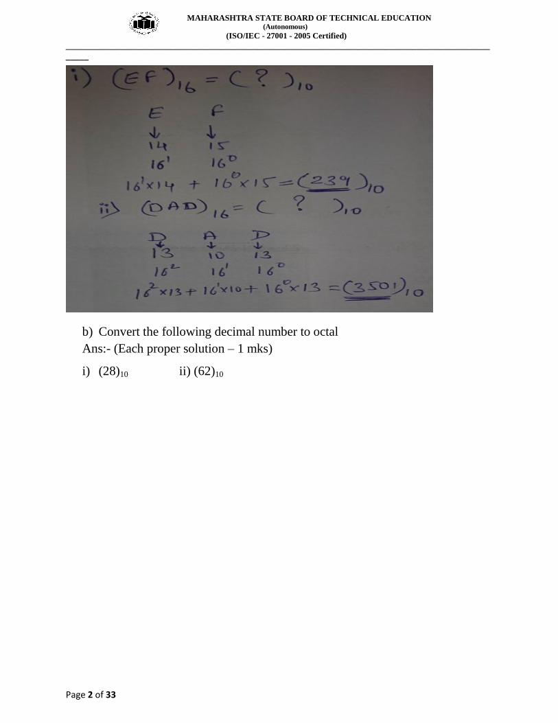
a) Convert the following hexadecimal number to decimal
i) (EF)16 Ii) ( DAD)16
Ans:- (Each proper solution – 1 mks)
17320
MAHARASHTRA STATE BOARD OF TECHNICAL EDUCATION (Autonomous)
(ISO/IEC - 27001 - 2005 Certified)
_____________________________________________________________________________________________
_____
Page 2 of 33
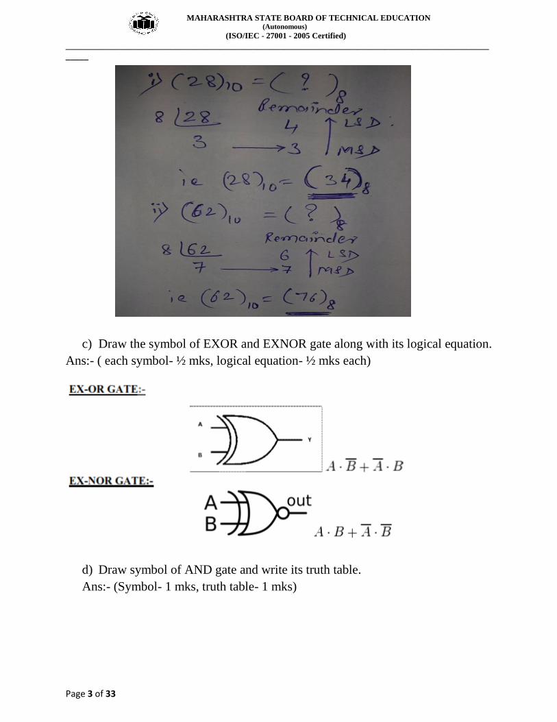
b) Convert the following decimal number to octal
Ans:- (Each proper solution – 1 mks)
i) (28)10 ii) (62)10
MAHARASHTRA STATE BOARD OF TECHNICAL EDUCATION (Autonomous)
(ISO/IEC - 27001 - 2005 Certified)
_____________________________________________________________________________________________
_____
Page 3 of 33
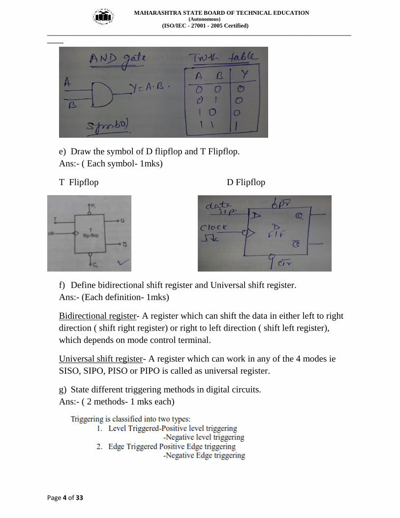
c) Draw the symbol of EXOR and EXNOR gate along with its logical equation.
Ans:- ( each symbol- ½ mks, logical equation- ½ mks each)
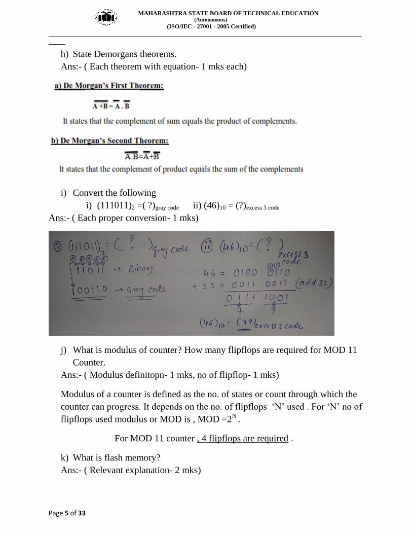
d) Draw symbol of AND gate and write its truth table.
Ans:- (Symbol- 1 mks, truth table- 1 mks)
MAHARASHTRA STATE BOARD OF TECHNICAL EDUCATION (Autonomous)
(ISO/IEC - 27001 - 2005 Certified)
_____________________________________________________________________________________________
_____
Page 4 of 33
e) Draw the symbol of D flipflop and T Flipflop.
Ans:- ( Each symbol- 1mks)
T Flipflop D Flipflop
f) Define bidirectional shift register and Universal shift register.
Ans:- (Each definition- 1mks)
Bidirectional register- A register which can shift the data in either left to right
direction ( shift right register) or right to left direction ( shift left register),
which depends on mode control terminal.
Universal shift register- A register which can work in any of the 4 modes ie
SISO, SIPO, PISO or PIPO is called as universal register.
g) State different triggering methods in digital circuits.
Ans:- ( 2 methods- 1 mks each)
MAHARASHTRA STATE BOARD OF TECHNICAL EDUCATION (Autonomous)
(ISO/IEC - 27001 - 2005 Certified)
_____________________________________________________________________________________________
_____
Page 5 of 33
h) State Demorgans theorems.
Ans:- ( Each theorem with equation- 1 mks each)
i) Convert the following
i) (111011)2 =( ?)gray code ii) (46)10 = (?)excess 3 code
Ans:- ( Each proper conversion- 1 mks)
j) What is modulus of counter? How many flipflops are required for MOD 11
Counter.
Ans:- ( Modulus definitopn- 1 mks, no of flipflop- 1 mks)
Modulus of a counter is defined as the no. of states or count through which the
counter can progress. It depends on the no. of flipflops ‘N’ used . For ‘N’ no of
flipflops used modulus or MOD is , MOD =2N
.
For MOD 11 counter , 4 flipflops are required .
k) What is flash memory?
Ans:- ( Relevant explanation- 2 mks)
MAHARASHTRA STATE BOARD OF TECHNICAL EDUCATION (Autonomous)
(ISO/IEC - 27001 - 2005 Certified)
_____________________________________________________________________________________________
_____
Page 6 of 33
l) Define resolution and linearity of DAC.
Ans:- ( Each relevant definition- 1 mks)
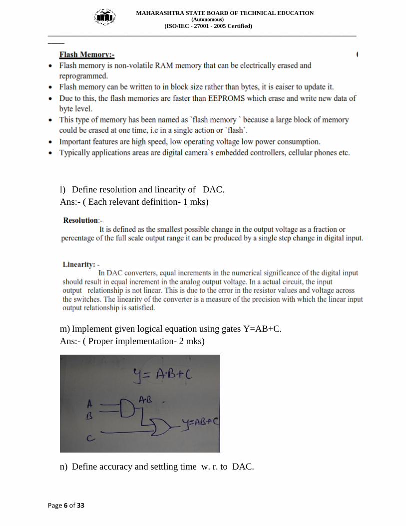
m) Implement given logical equation using gates Y=AB+C.
Ans:- ( Proper implementation- 2 mks)
n) Define accuracy and settling time w. r. to DAC.
MAHARASHTRA STATE BOARD OF TECHNICAL EDUCATION (Autonomous)
(ISO/IEC - 27001 - 2005 Certified)
_____________________________________________________________________________________________
_____
Page 7 of 33
Ans:- ( Each proper definition- 1 mks)
2 . Attempt any FOUR of the following 16
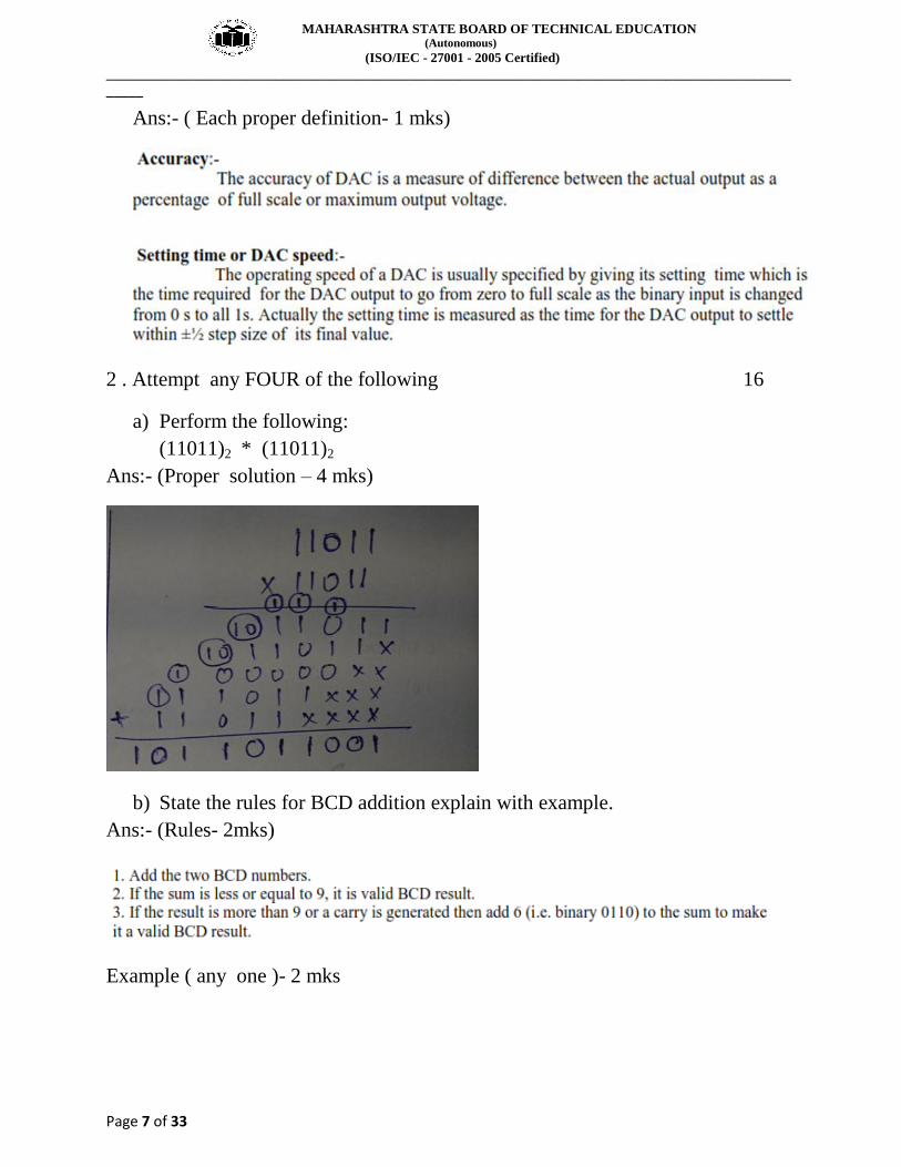
a) Perform the following:
(11011)2 * (11011)2
Ans:- (Proper solution – 4 mks)
b) State the rules for BCD addition explain with example.
Ans:- (Rules- 2mks)
Example ( any one )- 2 mks
MAHARASHTRA STATE BOARD OF TECHNICAL EDUCATION (Autonomous)
(ISO/IEC - 27001 - 2005 Certified)
_____________________________________________________________________________________________
_____
Page 8 of 33
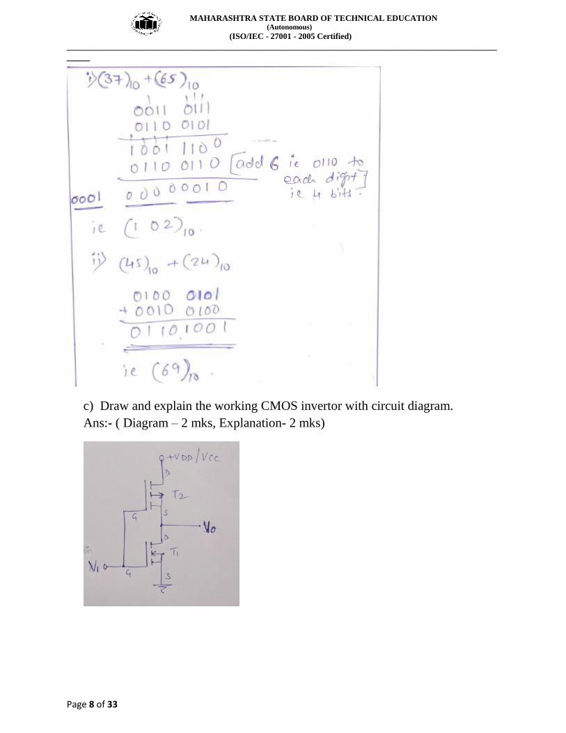
c) Draw and explain the working CMOS invertor with circuit diagram.
Ans:- ( Diagram – 2 mks, Explanation- 2 mks)
MAHARASHTRA STATE BOARD OF TECHNICAL EDUCATION (Autonomous)
(ISO/IEC - 27001 - 2005 Certified)
_____________________________________________________________________________________________
_____
Page 9 of 33
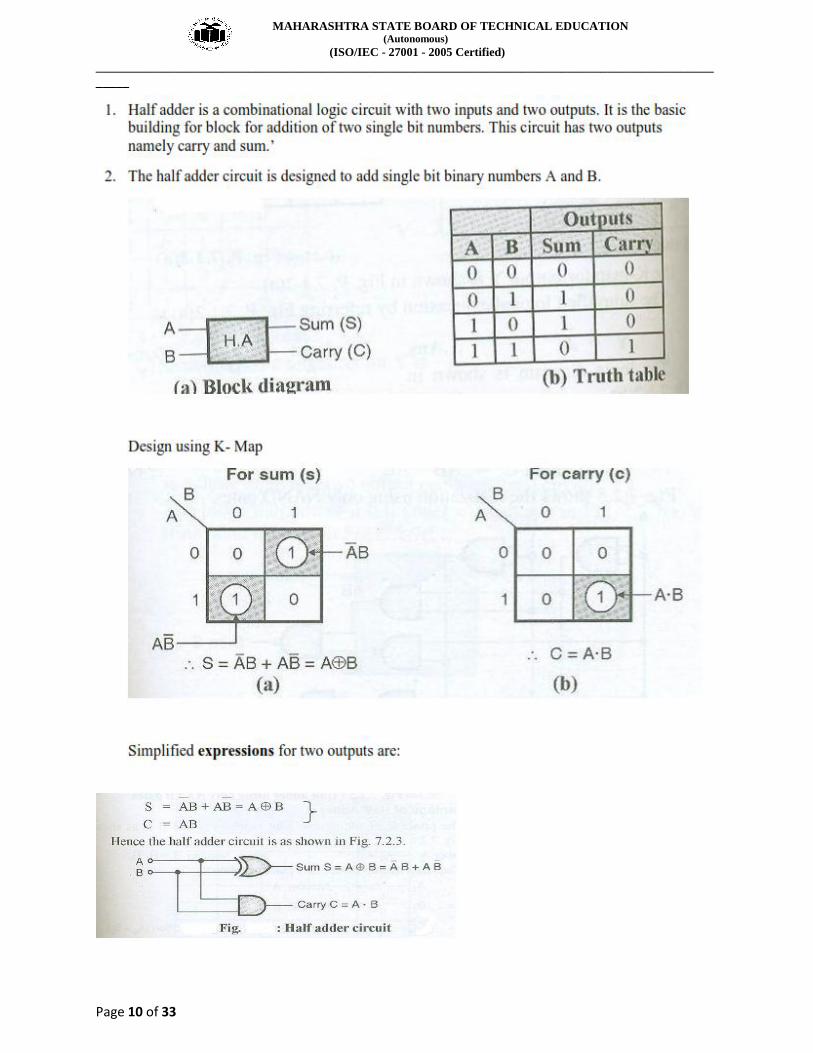
d) Design Half adder using K Map and implement using Gates.
Ans:-
MAHARASHTRA STATE BOARD OF TECHNICAL EDUCATION (Autonomous)
(ISO/IEC - 27001 - 2005 Certified)
_____________________________________________________________________________________________
_____
Page 10 of 33
MAHARASHTRA STATE BOARD OF TECHNICAL EDUCATION (Autonomous)
(ISO/IEC - 27001 - 2005 Certified)
_____________________________________________________________________________________________
_____
Page 11 of 33
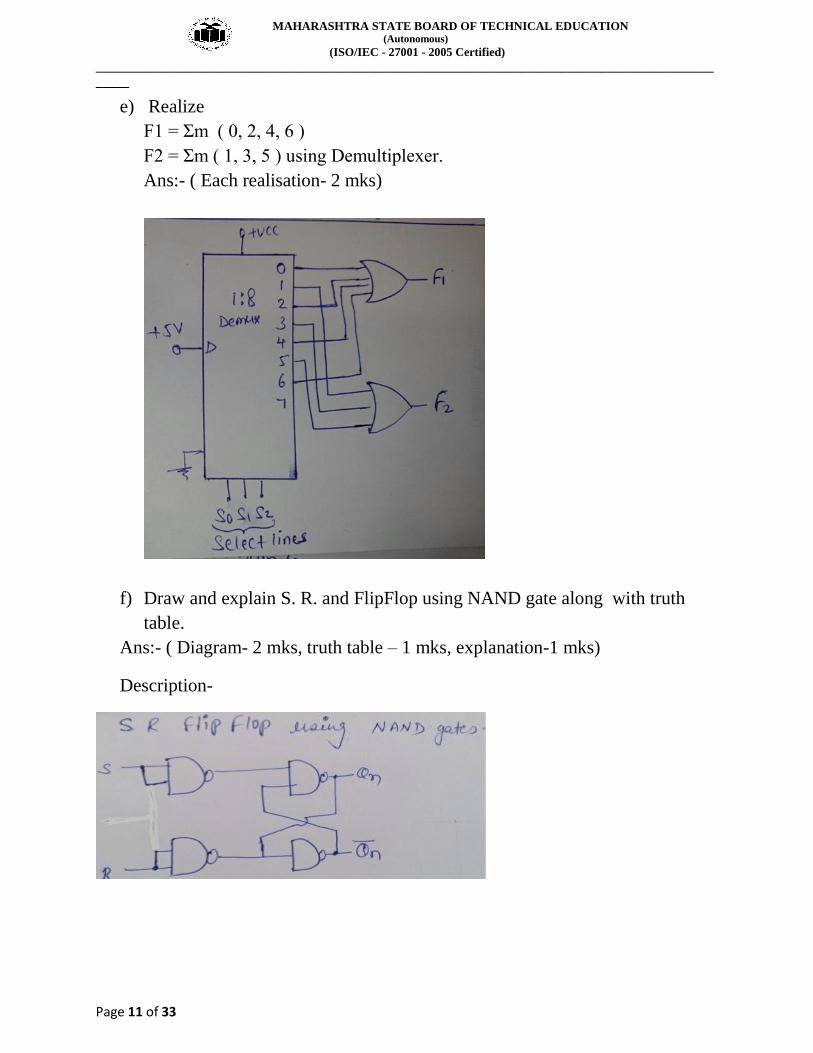
e) Realize
F1 = Σm ( 0, 2, 4, 6 )
F2 = Σm ( 1, 3, 5 ) using Demultiplexer.
Ans:- ( Each realisation- 2 mks)
f) Draw and explain S. R. and FlipFlop using NAND gate along with truth
table.
Ans:- ( Diagram- 2 mks, truth table – 1 mks, explanation-1 mks)
Description-
MAHARASHTRA STATE BOARD OF TECHNICAL EDUCATION (Autonomous)
(ISO/IEC - 27001 - 2005 Certified)
_____________________________________________________________________________________________
_____
Page 12 of 33
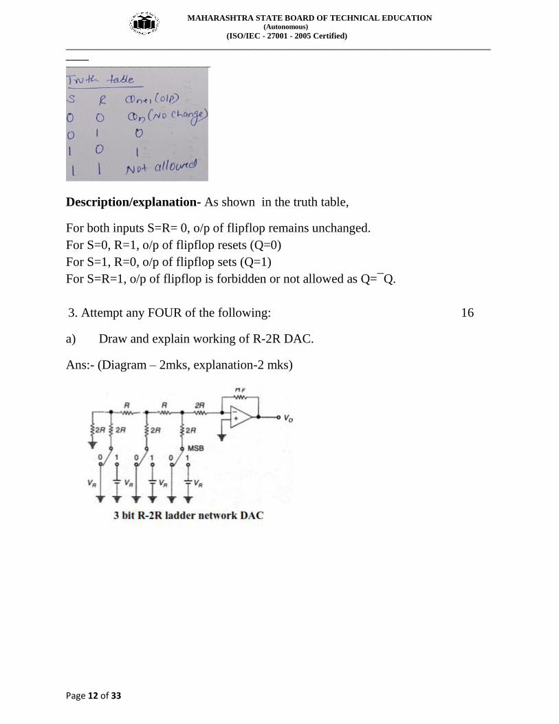
Description/explanation- As shown in the truth table,
For both inputs S=R= 0, o/p of flipflop remains unchanged.
For S=0, R=1, o/p of flipflop resets (Q=0)
For S=1, R=0, o/p of flipflop sets (Q=1)
For S=R=1, o/p of flipflop is forbidden or not allowed as Q=¯Q.
3. Attempt any FOUR of the following: 16
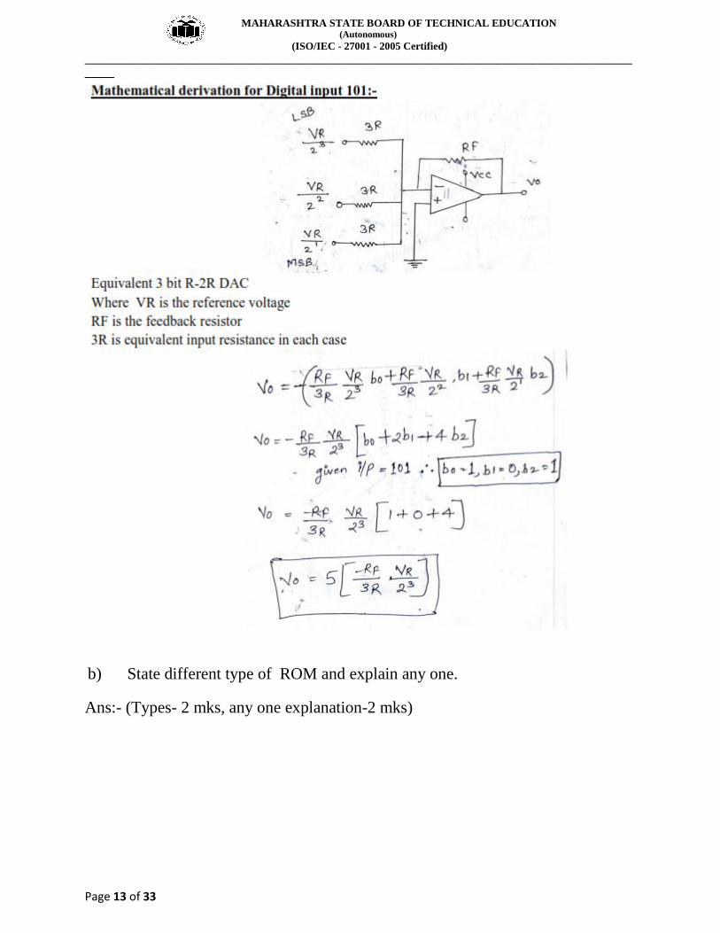
a) Draw and explain working of R-2R DAC.
Ans:- (Diagram – 2mks, explanation-2 mks)
MAHARASHTRA STATE BOARD OF TECHNICAL EDUCATION (Autonomous)
(ISO/IEC - 27001 - 2005 Certified)
_____________________________________________________________________________________________
_____
Page 13 of 33
b) State different type of ROM and explain any one.
Ans:- (Types- 2 mks, any one explanation-2 mks)

MAHARASHTRA STATE BOARD OF TECHNICAL EDUCATION (Autonomous)
(ISO/IEC - 27001 - 2005 Certified)
_____________________________________________________________________________________________
_____
Page 14 of 33
OR
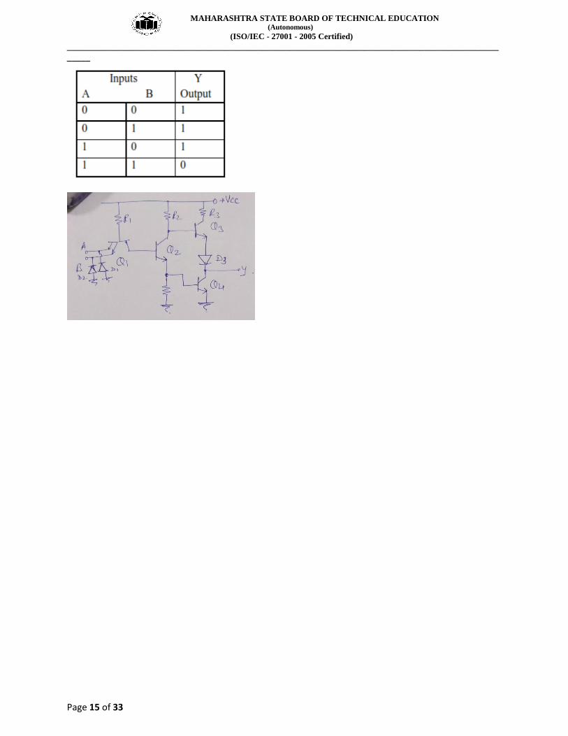
c) Draw circuit diagram of TTL NAND gate and explain its working.
Ans:- ( Diagram- 2 mks, truth table- 1 mks, explanation- 1 mks)
MAHARASHTRA STATE BOARD OF TECHNICAL EDUCATION (Autonomous)
(ISO/IEC - 27001 - 2005 Certified)
_____________________________________________________________________________________________
_____
Page 15 of 33

MAHARASHTRA STATE BOARD OF TECHNICAL EDUCATION (Autonomous)
(ISO/IEC - 27001 - 2005 Certified)
_____________________________________________________________________________________________
_____
Page 16 of 33
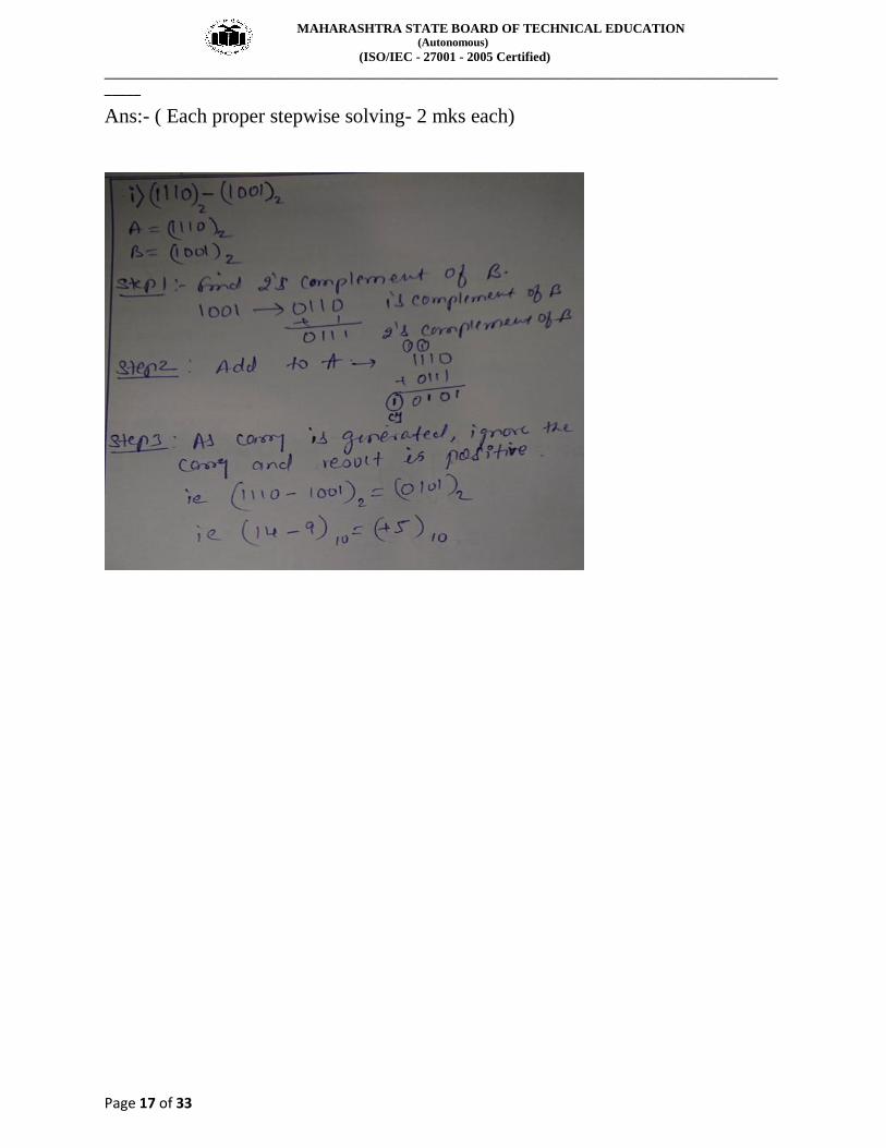
d) Subtract using 2’s complement method
(i) (1110)2 – (1001)2
(ii) (1000)2 – ( 1001)2
MAHARASHTRA STATE BOARD OF TECHNICAL EDUCATION (Autonomous)
(ISO/IEC - 27001 - 2005 Certified)
_____________________________________________________________________________________________
_____
Page 17 of 33
Ans:- ( Each proper stepwise solving- 2 mks each)

MAHARASHTRA STATE BOARD OF TECHNICAL EDUCATION (Autonomous)
(ISO/IEC - 27001 - 2005 Certified)
_____________________________________________________________________________________________
_____
Page 18 of 33
e) Draw Master Salve JF FlipFlop and write its truth table.
Ans:- ( Diagram- 2 mks, truth table- 2 mks)
MAHARASHTRA STATE BOARD OF TECHNICAL EDUCATION (Autonomous)
(ISO/IEC - 27001 - 2005 Certified)
_____________________________________________________________________________________________
_____
Page 19 of 33
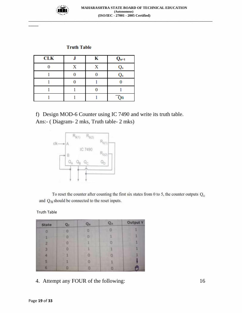
f) Design MOD-6 Counter using IC 7490 and write its truth table.
Ans:- ( Diagram- 2 mks, Truth table- 2 mks)
Truth Table
4. Attempt any FOUR of the following: 16

MAHARASHTRA STATE BOARD OF TECHNICAL EDUCATION (Autonomous)
(ISO/IEC - 27001 - 2005 Certified)
_____________________________________________________________________________________________
_____
Page 20 of 33
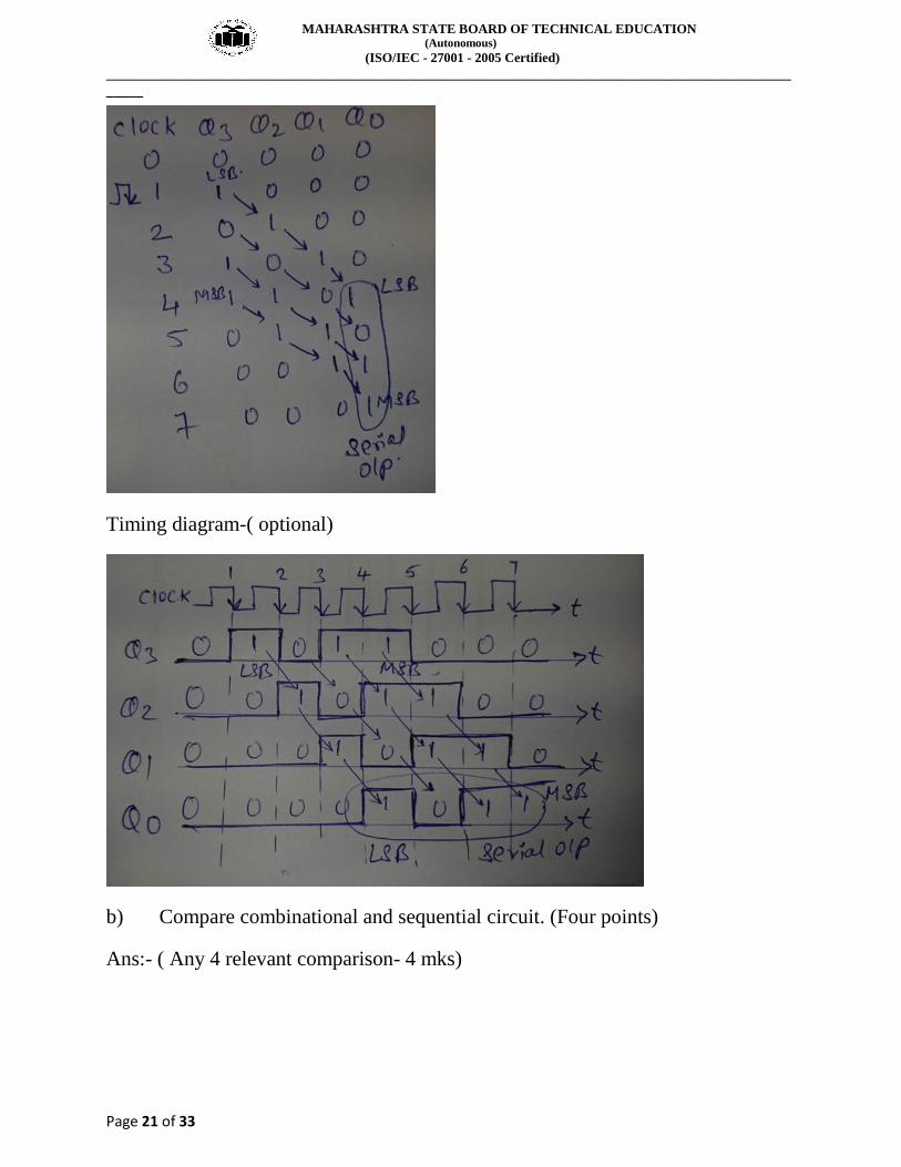
a) Describe working of SISO shift Register with proper circuit diagram.
Ans:- (Diagram- 2 mks, truth table 1 mks, describe/explain in short – 1
mks,waveform not compulsory, can be considered)
Description-As shown a 4 bit SISO shift register consists of 4 D flipflop , data is
fed from first flipflop and on application of clock pulses the data is shifted from
first flipflop to the last flipflop ,working as serial in and serial out shift register.
Let the data be -1101.
The truth table and timing diagram ( optional) is as shown below-
Truth Table
MAHARASHTRA STATE BOARD OF TECHNICAL EDUCATION (Autonomous)
(ISO/IEC - 27001 - 2005 Certified)
_____________________________________________________________________________________________
_____
Page 21 of 33
Timing diagram-( optional)
b) Compare combinational and sequential circuit. (Four points)
Ans:- ( Any 4 relevant comparison- 4 mks)
MAHARASHTRA STATE BOARD OF TECHNICAL EDUCATION (Autonomous)
(ISO/IEC - 27001 - 2005 Certified)
_____________________________________________________________________________________________
_____
Page 22 of 33
c) Compare :
(i) Volatile with Non-Volatile memory.
(ii) SRAM with DRAM memory.
Ans:- Volatile with Non-Volatile memory (any 2 points-2 mks)
SRAM with DRAM memory ( any 2 points- 2 mks)
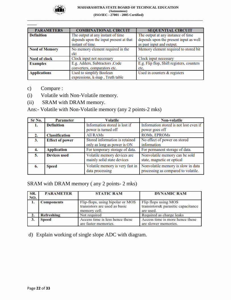
d) Explain working of single slope ADC with diagram.
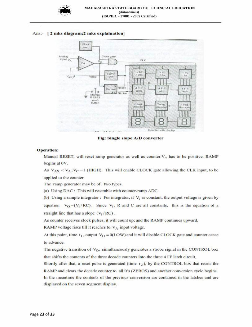
MAHARASHTRA STATE BOARD OF TECHNICAL EDUCATION (Autonomous)
(ISO/IEC - 27001 - 2005 Certified)
_____________________________________________________________________________________________
_____
Page 23 of 33
MAHARASHTRA STATE BOARD OF TECHNICAL EDUCATION (Autonomous)
(ISO/IEC - 27001 - 2005 Certified)
_____________________________________________________________________________________________
_____
Page 24 of 33
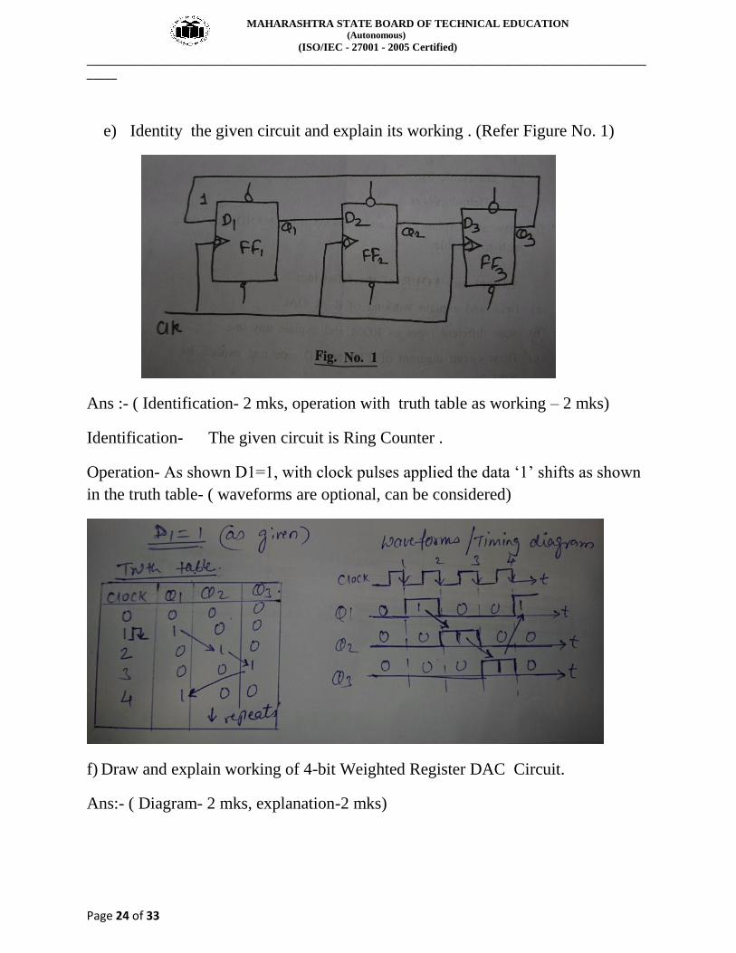
e) Identity the given circuit and explain its working . (Refer Figure No. 1)
Ans :- ( Identification- 2 mks, operation with truth table as working – 2 mks)
Identification- The given circuit is Ring Counter .
Operation- As shown D1=1, with clock pulses applied the data ‘1’ shifts as shown
in the truth table- ( waveforms are optional, can be considered)
f) Draw and explain working of 4-bit Weighted Register DAC Circuit.
Ans:- ( Diagram- 2 mks, explanation-2 mks)

MAHARASHTRA STATE BOARD OF TECHNICAL EDUCATION (Autonomous)
(ISO/IEC - 27001 - 2005 Certified)
_____________________________________________________________________________________________
_____
Page 25 of 33
5. Attempt any FOUR of the following: 16
MAHARASHTRA STATE BOARD OF TECHNICAL EDUCATION (Autonomous)
(ISO/IEC - 27001 - 2005 Certified)
_____________________________________________________________________________________________
_____
Page 26 of 33
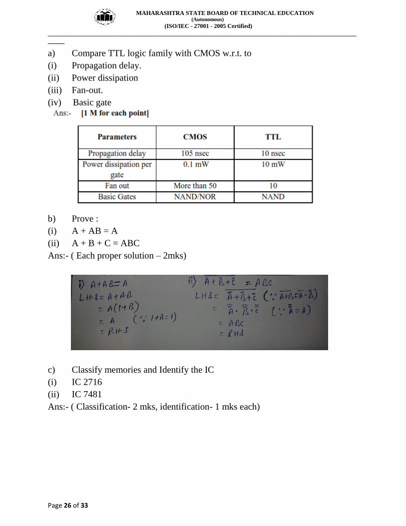
a) Compare TTL logic family with CMOS w.r.t. to
(i) Propagation delay.
(ii) Power dissipation
(iii) Fan-out.
(iv) Basic gate
b) Prove :
(i) A + AB = A
(ii) A + B + C = ABC
Ans:- ( Each proper solution – 2mks)
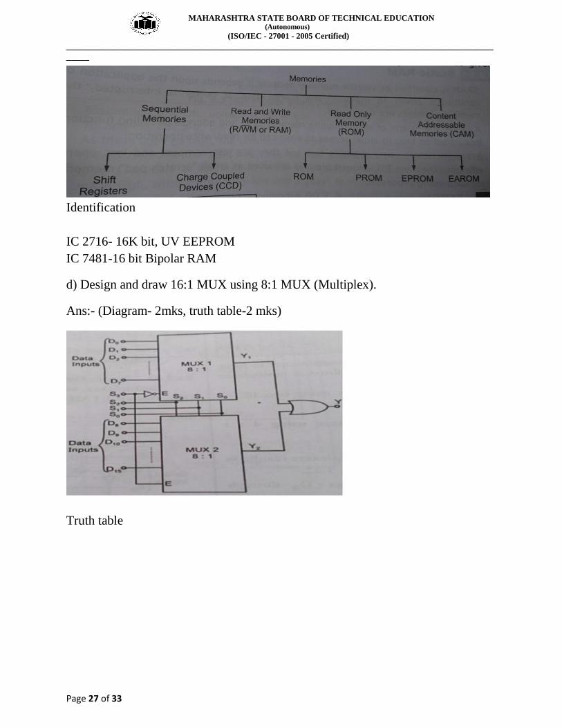
c) Classify memories and Identify the IC
(i) IC 2716
(ii) IC 7481
Ans:- ( Classification- 2 mks, identification- 1 mks each)
MAHARASHTRA STATE BOARD OF TECHNICAL EDUCATION (Autonomous)
(ISO/IEC - 27001 - 2005 Certified)
_____________________________________________________________________________________________
_____
Page 27 of 33
Identification
IC 2716- 16K bit, UV EEPROM
IC 7481-16 bit Bipolar RAM
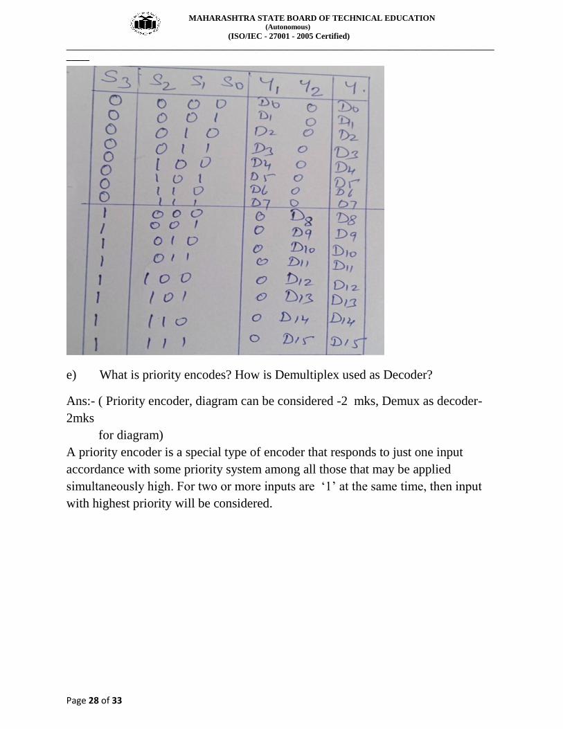
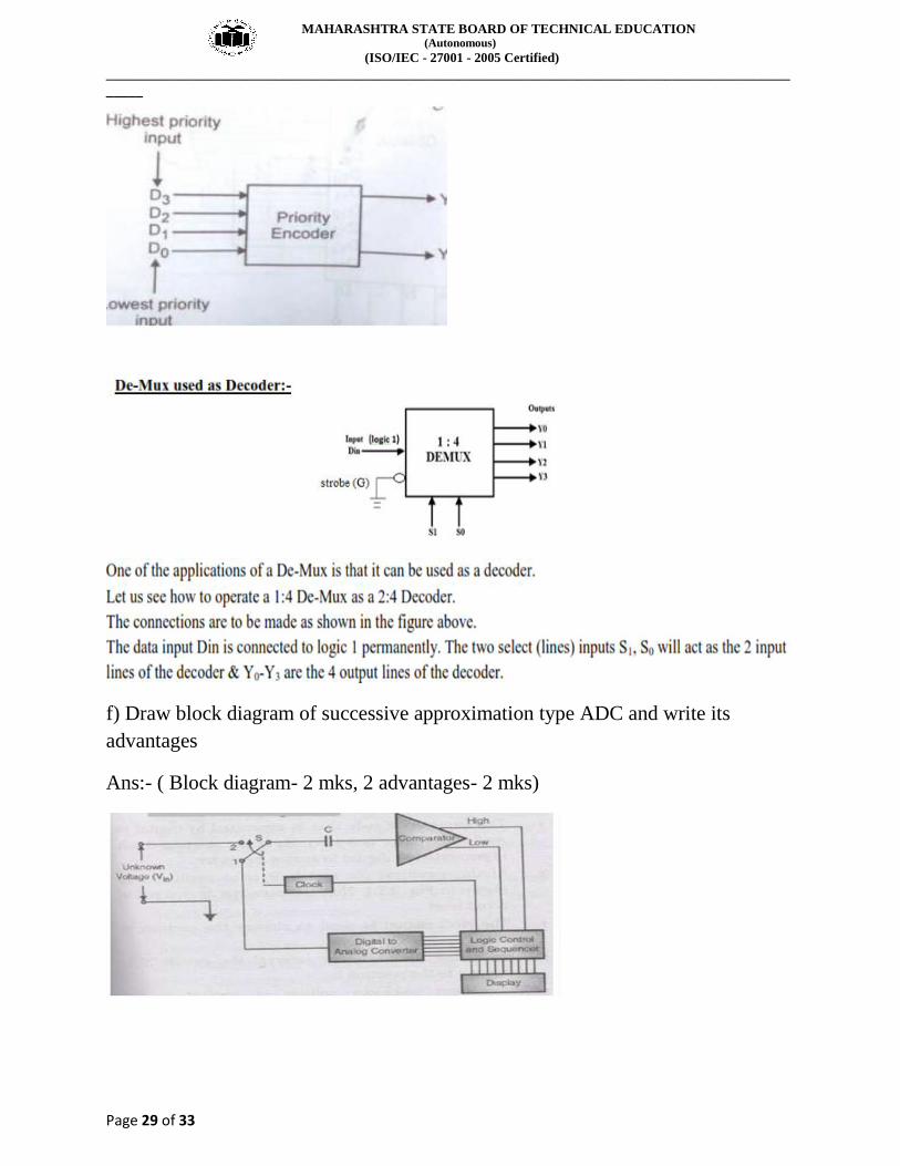
d) Design and draw 16:1 MUX using 8:1 MUX (Multiplex).
Ans:- (Diagram- 2mks, truth table-2 mks)
Truth table
MAHARASHTRA STATE BOARD OF TECHNICAL EDUCATION (Autonomous)
(ISO/IEC - 27001 - 2005 Certified)
_____________________________________________________________________________________________
_____
Page 28 of 33
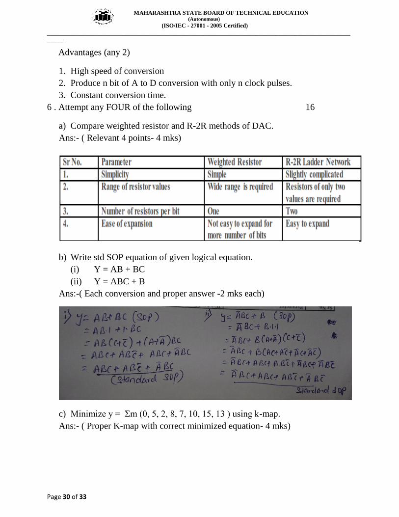
e) What is priority encodes? How is Demultiplex used as Decoder?
Ans:- ( Priority encoder, diagram can be considered -2 mks, Demux as decoder-
2mks
for diagram)
A priority encoder is a special type of encoder that responds to just one input
accordance with some priority system among all those that may be applied
simultaneously high. For two or more inputs are ‘1’ at the same time, then input
with highest priority will be considered.
MAHARASHTRA STATE BOARD OF TECHNICAL EDUCATION (Autonomous)
(ISO/IEC - 27001 - 2005 Certified)
_____________________________________________________________________________________________
_____
Page 29 of 33
f) Draw block diagram of successive approximation type ADC and write its
advantages
Ans:- ( Block diagram- 2 mks, 2 advantages- 2 mks)
MAHARASHTRA STATE BOARD OF TECHNICAL EDUCATION (Autonomous)
(ISO/IEC - 27001 - 2005 Certified)
_____________________________________________________________________________________________
_____
Page 30 of 33
Advantages (any 2)
1. High speed of conversion
2. Produce n bit of A to D conversion with only n clock pulses.
3. Constant conversion time.
6 . Attempt any FOUR of the following 16
a) Compare weighted resistor and R-2R methods of DAC.
Ans:- ( Relevant 4 points- 4 mks)
b) Write std SOP equation of given logical equation.
(i) Y = AB + BC
(ii) Y = ABC + B
Ans:-( Each conversion and proper answer -2 mks each)
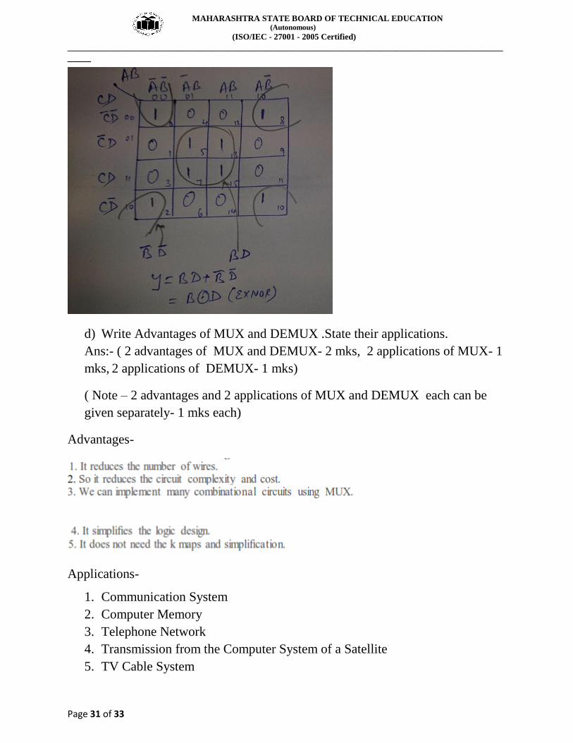
c) Minimize y = Σm (0, 5, 2, 8, 7, 10, 15, 13 ) using k-map.
Ans:- ( Proper K-map with correct minimized equation- 4 mks)
MAHARASHTRA STATE BOARD OF TECHNICAL EDUCATION (Autonomous)
(ISO/IEC - 27001 - 2005 Certified)
_____________________________________________________________________________________________
_____
Page 31 of 33
d) Write Advantages of MUX and DEMUX .State their applications.
Ans:- ( 2 advantages of MUX and DEMUX- 2 mks, 2 applications of MUX- 1
mks, 2 applications of DEMUX- 1 mks)
( Note – 2 advantages and 2 applications of MUX and DEMUX each can be
given separately- 1 mks each)
Advantages-
Applications-
1. Communication System
2. Computer Memory
3. Telephone Network
4. Transmission from the Computer System of a Satellite
5. TV Cable System

MAHARASHTRA STATE BOARD OF TECHNICAL EDUCATION (Autonomous)
(ISO/IEC - 27001 - 2005 Certified)
_____________________________________________________________________________________________
_____
Page 32 of 33
e) Identify the given circuit and write its truth table – Diagram below (Refer
Figure No.2)
Ans:- ( Identification- 2 mks, truth table-2 mks)
The given circuit is a MUX tree - 8:1 MUX using 4: 1 Mux .
Truth Table-
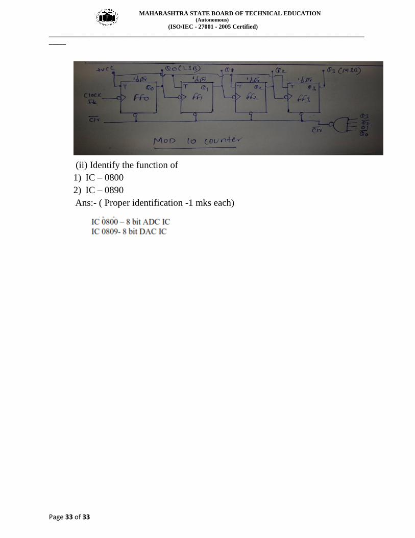
f) (i) Draw circuit diagram of MOD – 10 counter using T-FF.
Ans:- ( Proper detailed diagram-2 mks)
MAHARASHTRA STATE BOARD OF TECHNICAL EDUCATION (Autonomous)
(ISO/IEC - 27001 - 2005 Certified)
_____________________________________________________________________________________________
_____
Page 33 of 33
(ii) Identify the function of
1) IC – 0800
2) IC – 0890
Ans:- ( Proper identification -1 mks each)