wlf for high-performance ddr2 sdram and …s3.amazonaws.com/zanran_storage/ annual international kgd...
TRANSCRIPT

11th Annual International KGD Packaging and Test Workshop | September 12-15, 2004 | Napa, CA
WLF(Wafer-level Fabricated Package) for high-performance DDR2 SDRAM and
Memory ModuleGusungGusung Kim, Ph.DKim, Ph.D
Interconnect Product & Technology TeamInterconnect Product & Technology TeamMemory DivisionMemory Division
Semiconductor BusinessSemiconductor BusinessSamsung Electronics Co., Ltd. Samsung Electronics Co., Ltd.
EE--mail: mail: [email protected]@samsung.comPhone : 1Phone : 1--8282--1111--797797--62536253

11th Annual International KGD Packaging and Test Workshop | September 12-15, 2004 | Napa, CA
Co-Authors @ Samsung Electronics Co., Ltd.
Interconnection Product & Technology TeamSM. Shim, DH. Jang, HS Chung, JS. Chung, JJ. Lee, SD. Baek, JH. Baek, JH. Lee, IY. Lee, MS. Park, YH. Song, SY. Oh
Test Team and Module TeamJI. Lee, YH. Kim, SH. Park, JH. Bang, SD. Choi
Quality Assurance TeamGK. Kang
AcknowledgementAcknowledgement
11th Annual International KGD Packaging and Test Workshop | September 12-15, 2004 | Napa, CA
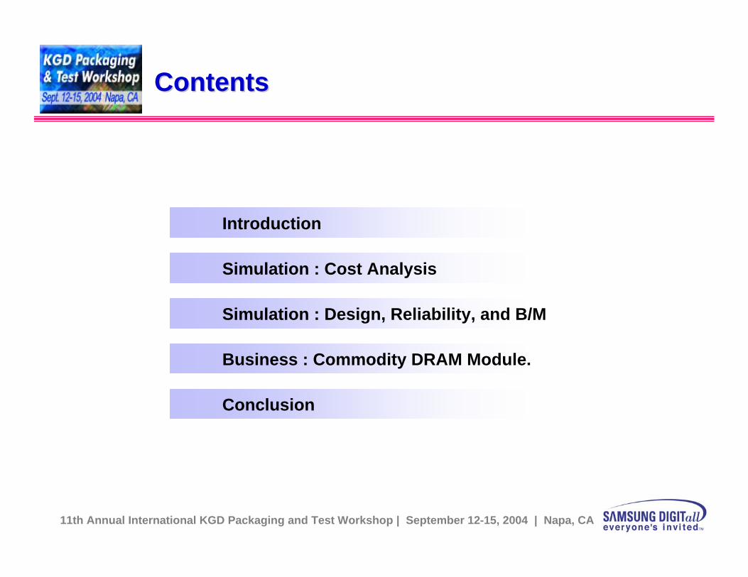
Contents Contents
Introduction
Simulation : Cost Analysis
Simulation : Design, Reliability, and B/M
Conclusion
Business : Commodity DRAM Module.

11th Annual International KGD Packaging and Test Workshop | September 12-15, 2004 | Napa, CA
Denser! Denser!Denser! Denser!

11th Annual International KGD Packaging and Test Workshop | September 12-15, 2004 | Napa, CA
0.2mm0.3mm0.3mm0.4mm0.4mmFBGA/CSP Solder Ball Pad Pitch
120 um130 um130 um150 um150 umFlip Chip Pad Pitch
←←5 Chip5 Chip4 ChipDie Stack for SIP
85oC85oC85oC90oC90oCJunction Temperature Max.(Cost Performance)
0.2mm0.3mm0.3mm0.4mm0.4mmFBGA/CSP Solder Ball Pad Pitch
65nm70nm80nm90nm107nmMPU / ASIC ½ Pitch
BGA Solder Ball Pitch (Cost Performance)
Peripheral Flip Chip
Flip Chip Area Array
Wire Bonding Pitch - Wedge
Wire Bonding Pitch - Ball
Minimum Overall PKG Profile (Cost Performance)
Pincount Maximum (Cost Performance)
Power : Single Chip PKG (Cost Performance)
Wafer Size
DRAM ½ Pitch
Year of Production
20um20um20um25um30um
25um25um30um35um40um
0.8mm0.8mm0.8mm0.8mm1.0mm
3040406060
0.65mm0.65mm0.65mm0.8mm0.8mm
120130130150150
600-2140550-1936550-1760500-1600500-1452
0.74 W/mm20.7 W/mm20.65W/mm20.6 W/mm20.57W/mm2
300mm300mm300mm300mm300mm
65nm70nm80nm90nm100nm
2006 2007 200520042003
2003 ITRS Roadmap2003 ITRS Roadmap
Technical RoadmapTechnical Roadmap

11th Annual International KGD Packaging and Test Workshop | September 12-15, 2004 | Napa, CA
WLWL--CSP Applications CSP Applications

11th Annual International KGD Packaging and Test Workshop | September 12-15, 2004 | Napa, CA
Market Status Market Status @ Memory Device@ Memory Device
New WLP Flow for Low Cost (Infineon)
EDS
Fuse Repair
WL Process Back-grind/ Coating/ Ball Mount
WLBI
WLT (@Speed)
Sawing
WLP Test (DC Test)
V/I, MarkingModule Ass’y
F/O
Wafer
Infineon Samsung
Test & B/I Contact
Atmel, XicorEEPROM Biz.
Fujitsu Flash Memory (Shinko)
Super CSP Casio Wrist-Watch / Camera
Hitachi 64M SDRAM WLP
Casio EXILIM(EX-SI) , Camera
Micron 256M SDRAM WLP
High Density Solution
TwinMOS / ACET
DDR 512MB SO-DIMM / RDIMM
WLP Biz. Status

11th Annual International KGD Packaging and Test Workshop | September 12-15, 2004 | Napa, CA
Process SimplifyProcess Simplify
PadPadRedistributionRedistribution
ILD1 layer deposition and patterning
ILD2 layer deposition and patterning Reflow solder
Sputter metals and etch to form trace and pad

11th Annual International KGD Packaging and Test Workshop | September 12-15, 2004 | Napa, CA
Process Application Process Application –– PoCPoC based DDPbased DDP
PoC (Pad-on-Circuit) Process
(Source : 10th KGD Workshop)
1Gb DDR 333 (11.5 x 12)

11th Annual International KGD Packaging and Test Workshop | September 12-15, 2004 | Napa, CA
Cost Effective Solution than current packageNew Package Solution Low Assembly Cost ( Target : ?% Down )
High Reliability (Back-side Coating, Joint Reliability)Design Guide (w Underfill, w/o Underfill)
High Speed Design Availability533 Mbps Approved
Thermal Solution for High Speed DDRDie per Wafer (Yield) / JEDEC Standardization
Business BaselineBusiness Baseline
Ball Matrix SolutionJEDEC Standardization
Market Driven Product (Component and Commodity Memory Module)Benchmark
WFP
Business
Project

11th Annual International KGD Packaging and Test Workshop | September 12-15, 2004 | Napa, CA
5um / 1.7umOptionalMin.10um / Min.5umRDL Width/Thickness
Wire BondingSolder Bump (f100um)Ball / Wire BondingInterconnection
End-FabricationUBM + Bump WL ProcessComment
NoneTi/Ni/NiCr/Cu/Cu/Ni/(Au)UBM
Al / SputteringOptional Cu/Ni/(Au), Plating RD Metal/Method
Pass’n (SiN) / 0.7umPI / 7.5umPI or BCB /~10umILD2 Material/Thickness
IMDOptionalPI or BCB /~10umILD1 Material/Thickness
Back-EndFlip ChipWFP / POCItem
Structure (WFP/Structure (WFP/PoCPoC))

11th Annual International KGD Packaging and Test Workshop | September 12-15, 2004 | Napa, CA
Wafer Level Processing
Wafer Level Processing
Laser MarkLaser Mark
Wafer Back-grindWafer Back-grind
Wafer Mount/Saw
Wafer Mount/Saw
Visual InspectVisual Inspect
Pick & Place to Tape or Tray
Pick & Place to Tape or Tray
Pack & Ship DiePack & Ship Die
Wafer ProbeWafer Probe
WBI (*)EDS
WBI (*)EDS
Wafer BizWFP Biz
Module Biz
Wafer BizWFP Biz
Module Biz
Mask Design(RDLed)
Mask Design(RDLed)
Wafer Back-grindWafer Back-grind
Backside CoatingBackside Coating
DicingDicing
WFP Test(Ball)(B/I), Speed SortWFP Test(Ball)
(B/I), Speed Sort
V/I & MarkingV/I & Marking
Wafer Back-grindWafer Back-grind
Backside CoatingBackside Coating
Wafer Test (Ball)*(B/I), @Speed
Wafer Test (Ball)*(B/I), @Speed
DicingDicing
V/I & MarkingV/I & Marking
L/RepairL/Repair
WFP Test(DC Test)
WFP Test(DC Test)
WFP Process SimulationWFP Process Simulation
Cost SimulationCost Simulation

11th Annual International KGD Packaging and Test Workshop | September 12-15, 2004 | Napa, CA
WFP Solves the Cost Paradigm of the BackWFP Solves the Cost Paradigm of the Back--EndEnd
Source : IMAPS Conference (’03 / Infineon Data)
Cost SimulationCost Simulation

11th Annual International KGD Packaging and Test Workshop | September 12-15, 2004 | Napa, CA
Estimated WFP Cost SimulationEstimated WFP Cost Simulation
0.8
0.58
0.36 0.33 0.31 0.29
1.1
1
0.8250.77 0.74
0.7
0
0.1
0.2
0.3
0.4
0.5
0.6
WBGA BOC WLP-1 WLP-2 WLP-3 WLP-40
0.2
0.4
0.6
0.8
1
1.2Ass'y
Test
Comp_Total
Cum
80%70%60%FAB Yield
52%71%88%FAB Mat’l Portion
12”(1200ea)
8”(600ea)256M
DDR
12”(650ea)
8”(300ea)512M
DDR
12”(600ea)
8”(250ea)512M
DDR2
WFP Approach (Cost factor)
8”(800ea)
128MDDR
Net Die (300ea, Fab Yield 90%)WFP1 : 300ea, Yield 90% / WFP2 : 400, Yield 90% / WFP3 : 500ea, Yield 90% / WFP4 : 600ea, Yield 90%
Include EDS Cost
Include Module Cost
Cost SimulationCost Simulation

11th Annual International KGD Packaging and Test Workshop | September 12-15, 2004 | Napa, CA
DRAMsDRAMs : A Logical Choice for Fan: A Logical Choice for Fan--In WFPIn WFP
Ball Matrix SimulationBall Matrix Simulation

11th Annual International KGD Packaging and Test Workshop | September 12-15, 2004 | Napa, CA
JEDEC BallJEDEC Ball--out Matrix (For Fanout Matrix (For Fan--In WFP )In WFP )
OOOOFan-outOB
OOOOFan-outOA512M
XOnly X4/8Only X4/8OFan-outFan-outB
XOnly X4/8Only X4/8OFan-outFan-outA256M
0.8mm0.65/0.5mm0.65mm0.5mm84Ball60Ball
New Ball-out (X/Y Ball Pitch)JEDEC StandardPackageDevice
Ball Matrix SimulationBall Matrix Simulation

11th Annual International KGD Packaging and Test Workshop | September 12-15, 2004 | Napa, CA
Accumulated Reliability Data for WFP and Accumulated Reliability Data for WFP and CSPCSP’’ss
WFP Board Level Reliability Data – from 72/144M RDD to 256M DDR2Back-Side Protection – Updated CSP’sMemory Module Reliability – “Mechanical Test”Need Underfill and Back-side Protection
Reliability SimulationReliability Simulation

11th Annual International KGD Packaging and Test Workshop | September 12-15, 2004 | Napa, CA
Reliability Items in SamsungReliability Items in Samsung
Reliability SimulationReliability Simulation
1000cyc(Option-
Insitu)(Option)(Option)(Option)(Option)
-25C – 125C1500G,0.5ms JEDEC104B.Cond. B5mm,1Hz,4-pt,25mm~85mm,Sine
40mm(3.2m/s) to 5mm, B/F20G, 20-2KHz
11ms, 50G, 5Shock, 6 axisTBDTBD
20mdl(160)7mdl
20mdl20mdl
140mdl(1120) 140mdl(1120)140mdl(1120)140mdl(1120)
MDL TCDrop
Bend FatigueBend Impact
VibrationShockTwistBend
ModuleReliability
ESDLatch-up
HTSTC
PCTTHB
HAST
Test Items
200 (3)200 (3)
120 (3)120 (3)120 (3)120 (3)120 (3)
S/S (Run)
HBM2000V, MM200V, CDM500VJEDEC Std.
150C, No Bias-55C – 125C
121C, 100%, 2atm85C,85%,1.8V static Bias
130C, 85%
Test Condition
-
1000cyc168hrs1008hrs1008hrs
R/O
ComponentReliability
BaselineEvaluation
Categories

11th Annual International KGD Packaging and Test Workshop | September 12-15, 2004 | Napa, CA
EEPROMEEPROM
CIS256M DDR
64M SDRAMDDR2
256M SDRAMDevice
Mobile systemMobile systemWrist-Watch / CameraMemory Module (ACE, TwinMOS, GEIL)Mobile system Memory High Density solutionMemory High Density solution
Remark
AtmelCasio
Hitachi Infinion
ACET
Foundry
Xicor
MicronIDM
Company
Benchmark SimulationBenchmark Simulation

11th Annual International KGD Packaging and Test Workshop | September 12-15, 2004 | Napa, CA
0
500
1000
1500
2000
2500
3000
3500
4000
4500
1998 1999 2000 2001 2002 2003 2004 2005 2006
512Mb
1GB
2GB
4GB
512MB256Mb
1Gb
128Mb
DR
AM
Den
sity
Mod
ule
Den
sity
(RD
IMM
)
• RDIMM : Registered Dual In-line Memory Module
TSOP Stack / sTSOP
Solution ?(’03 ~ )
DRAM Density (Mono Die)Module Trend (Mono Die)Module Trend (Customer Requirement)
Business : Commodity DRAM ModuleBusiness : Commodity DRAM Module
DRAM Density TrendDRAM Density Trend

11th Annual International KGD Packaging and Test Workshop | September 12-15, 2004 | Napa, CA
Commodity DRAM ModuleCommodity DRAM Module
WFP1.2”DDR2
New Package Solution !

11th Annual International KGD Packaging and Test Workshop | September 12-15, 2004 | Napa, CA
Structure (WFP vs. BOC) Structure (WFP vs. BOC)
11.00x13.00x1.10 mm3 (A :100%)9.45x10.33x0.85mm3 (A : 68%)Package Size(W x D x H)
- Fan-Out - Chip Out Protection- High Frequency Applicable-Low Cost and Structure Expendability
- High Frequency Applicable- Good Thermal Dissipation- Design Availability- Low Cost
Pros
- Slightly Thermal Degradation- Design Limit for Mold outline
- Only Fan-In- Protector NeededCons
PackageStructure
60BOC60WFPItems
Chip

11th Annual International KGD Packaging and Test Workshop | September 12-15, 2004 | Napa, CA
System Process MapSystem Process Map
S I P O CMaterialsPlanning
InfrastructureWaferEDS
Customer NeedsPackage Trend
StructurePoC Design
Wire
CustomerFinal Shipping
Design Spec.Bondability
ProcessMargin
WLT & WLBI
WFP Scheme
PhotoMetal/Etch
Solder Mount
EDS
Dicing
P.T.
Elec. SimulationMech. Simulation
Infrastructure
SMT MethodInfrastructure
Wafer Probing
Instruction
PackageDesign Spec.
Process Spec.
EVALUATION
Qualification

11th Annual International KGD Packaging and Test Workshop | September 12-15, 2004 | Napa, CA
Yes
Reject
ILD1 thickness
Run start
ILD1 pattern
ILD1 cure
Base Metal sputter
P.R. pattern
Metal E.P.
Metal thickness
Base Metal etch
Metal Line lifting
Run out
Yes
No
Yes
Yes
Reject
Outputs
• ILD1 Thickness• ILD1 Uniformity• Fuse open• Repair yield• Metal line THK • Metal Line Width• ILD2 Thickness• ILD2 Uniformity• Bump shear Test• Bump Pull Test
Inputs•WFP Design (X)•ILD Mat’l (X)•Coating Spin rpm (X)•Soft Bake Time (X)•Hold Time af. Exposure (X)•Exposure Intensity (X)•Dev. Time (X)•Dev. Method (C)•Cure Temp (X)•Cure Time (X)•Cure Envior. (C)•Metal Mat’l (C)•Sputter Metal (C)•Sputter Metal THK (X)•Base Metal Etch Time (X)•Base Metal Etch Temp (X)•Base Metal Etch Method (X)•E.P. layer Structure(X)•E.P. Time (X)•E.P. Temp (X)•Descum Method(X)•Surface Treatment (X)•Design Check (X)•Mask Mfg. (X)
P.R. pattern
Metal E.P.
ILD2 thickness
BST
ILD2 pattern
ILD2 cure
Yes
Yes
Descum
Solder Ball Mount
Reflow
Flux Clean
Reject
Reject
※ X: Controllable, C: Constant N: Noise
Process Design ConceptsProcess Design Concepts

11th Annual International KGD Packaging and Test Workshop | September 12-15, 2004 | Napa, CA
1 2 3 4 5 6 7 8 9 10
Proj
ect
Y(K
POV)
Hei
ght
Stre
ngth
10 10
Pro jec t X (KPIV) Score1 Des ign 3 2 502 ILD Material 5 5 1003 ILD1 Thickness 10 2 1204 Metal Material 2 6 805 Metal Thickness 5 4 906 ILD Coater Spin Speed 10 7 1707 ILD Bake Temperature 9 4 1308 ILD Cure Time 4 1 509 ILD Develop Time 10 6 16010 ILD Exposure 5 1 6011 Descum Method 3 1 4012 Descum Time 3 1 4013 Chemical Treatment 3 10 13014 Au ELP 2 4 6015 Metal Milling Method 2 7 9016 Metal Milling Time 4 10 14020
View Results
Delete
데모
결과보기
지우기
Potential XPotential X’’ss
Customer KPIV Score %Score
Des ign 50 3.31%
ILD Material 100 6.62%
ILD1 Thickness 100 7.95%
Metal Material 80 5.30%
Metal Thickness 90 5.96%ILD Coater Spin Speed 170 11.26%
ILD Bake Temperature 130 8.61%
ILD Cure Time 50 3.31%
ILD Develop Time 120 10.60%ILD Exposure 60 3.97%
Descum Method 40 2.65%
Descum Time 40 2.65%Chemical Treatment 130 8.61%
Au ELP 60 3.97%Metal Milling Method 90 5.96%
Metal Milling Time 140 9.27%
• Pareto Chart from PFD, C&E Diagram, FMEA & FDM, Benchmarking

11th Annual International KGD Packaging and Test Workshop | September 12-15, 2004 | Napa, CA
CC--E Diagram E Diagram (Case Study)(Case Study)
Re-Reflow process
Material
MachineMethod
Design
ILD MaterialILD Thickness
Metal Material
Pad Structure
Ball Placement
Flux Dotting
Bump Shear Strength
Rerouting Pad Location
Metal Thickness
Au ELP , EP
Polyimide Etch
ILD Ash
PR Strip - Metal Etch
Cu/Ni ElectroplatingBump Shear Strength
Bonding Tool
USG Flux Process Condition
Photo-Litho.
PR Coat
Chemical
Descum
Gas
Plating Solution
Bonding Placement Fail
Electrical Performance PSPI & Posi-PRRDLed DesignBump Shear Strength
Solder
Bonding Temperature
Chemical Condition
Flux
SputterBonding Condition
Metal Contamination
ILD Profile
ILD Thickness
Metal Thickness
StrengthStrength

11th Annual International KGD Packaging and Test Workshop | September 12-15, 2004 | Napa, CA
533 66740060
65
70
75
80
85
90
95
100
105
Junc
tion
Tem
pera
ture
(o C)
Operating Speed(Mbps)
BOC@1m/sec BOC@2m/sec WLP@1m/sec WLP@2m/sec WLP+HS@1m/s WLP+HS@2m/s WLP+HK300@2m/s
Thermal PerformanceThermal Performance
Thermal Solution (35C & 2m/sec)Thermal Solution (35C & 2m/sec)
BOCWFP

11th Annual International KGD Packaging and Test Workshop | September 12-15, 2004 | Napa, CA
Wafer Level Package is one of the Market Driven Technologies
Package Differentiator
High Performance Solution
– WFP for memory devices
ConclusionsConclusions
DDR2 512MB UDIMM, non-ECC

11th Annual International KGD Packaging and Test Workshop | September 12-15, 2004 | Napa, CA
Wafer Biz. / MCP Solution : Added WFPDRAM
Wafer BizSRAM
Wafer BizMCP
Product
SRAM, FLASH
DRAM, SRAM, FLASH
DRAM, SRAM, FLASH
DRAM, SRAM, FLASH
DRAM, SRAM, FLASH
KGD for MCP and SIP Solution : WFP is a Solution for KGD
FLASH Wafer Biz
NOR, NAND
NOR
NOR, NAND
NOR
ConclusionsConclusions

11th Annual International KGD Packaging and Test Workshop | September 12-15, 2004 | Napa, CA
PartnershipPartnership