wavefront analysis with a shack-hartmann sensor using a ... · download/view course materials (note...
TRANSCRIPT
F36 experiment update July 2019
Wavefront Analysis with a Shack-Hartmann Sensor using a modern CMOS imager
This memo describes the most important changes in the F36 experiment setup and operations since 15 July 2019.
Hardware changes: the old CCD camera has been replaced with a new CMOS camera with approx. 20 M pixels (model ZWO ASI183 MM).
The new camera connects via USB3 to another new PC running a current Ubuntu system.
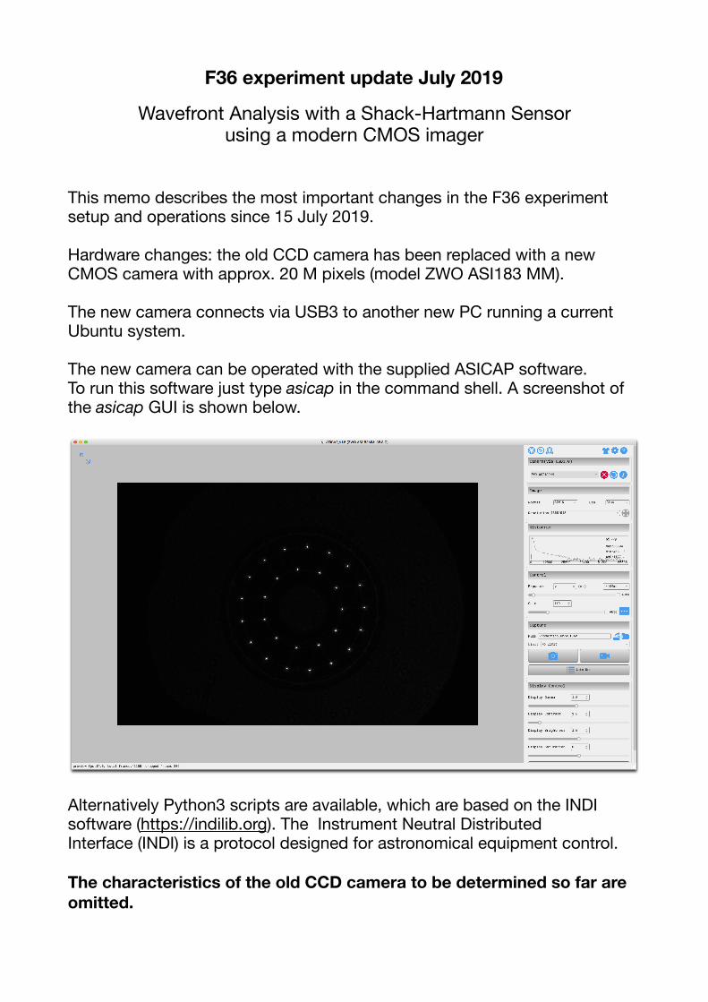
The new camera can be operated with the supplied ASICAP software.To run this software just type asicap in the command shell. A screenshot of the asicap GUI is shown below.
Alternatively Python3 scripts are available, which are based on the INDI software (https://indilib.org). The Instrument Neutral Distributed Interface (INDI) is a protocol designed for astronomical equipment control.
The characteristics of the old CCD camera to be determined so far are omitted.
Instead, only the CMOS camera system gain, i.e. the conversion factor of measured pixel values in ADU to photoelectrons, is to be determined. Alternatively, a physical explanation of the so-called photon transfer curve at the black board is sufficient.
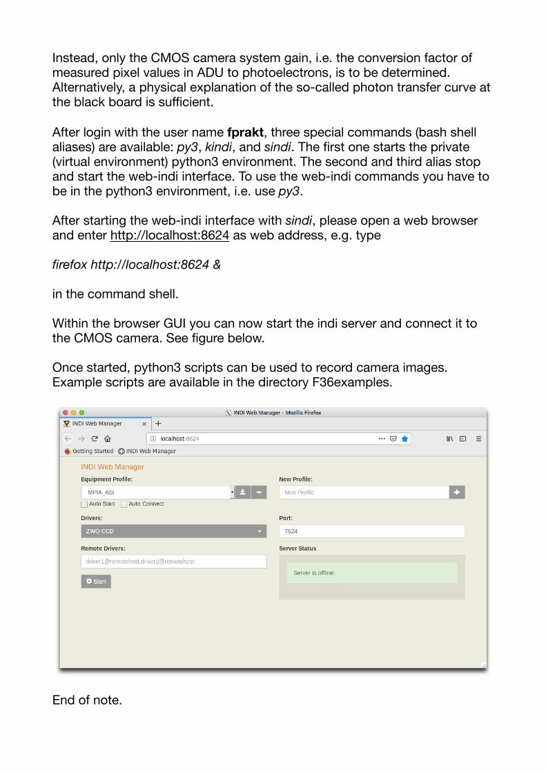
After login with the user name fprakt, three special commands (bash shell aliases) are available: py3, kindi, and sindi. The first one starts the private (virtual environment) python3 environment. The second and third alias stop and start the web-indi interface. To use the web-indi commands you have to be in the python3 environment, i.e. use py3.
After starting the web-indi interface with sindi, please open a web browser and enter http://localhost:8624 as web address, e.g. type
firefox http://localhost:8624 &
in the command shell.
Within the browser GUI you can now start the indi server and connect it to the CMOS camera. See figure below.
Once started, python3 scripts can be used to record camera images. Example scripts are available in the directory F36examples.
End of note.
16.07.19, 09)33Advanced lab course F36 at MPIA
Page 1 of 1http://www2.mpia.de/AO/INSTRUMENTS/FPraktikum.html
Wavefront analysis with a Shack-Hartmannwavefront sensorWellenfrontanalyse mit einem Shack-HartmannWellenfrontsensor
Advanced lab course for physics and astronomystudents of the University of Heidelberg atMPIA - lab course F36 Fortgeschrittenen-Praktikum für Studierende der Physik und Astronomieder Universität Heidelberg am MPIA - Versuch F36
Download/view course materials (note last update July 2019).Schedule overview and available dates during the semester break.
Further materials (in pdf format)
Adaptive Optik für die Astronomie, Augenheilkunde, Hochenergielaserund mehr, von Stefan Hippler, Markus Kasper, Ric Davies und RobertoRagazzoni. In german language.
Adaptive Optics on Large Telescopes, by Andreas Glindemann, StefanHippler, Thomas Berkefeld, and Wolfgang Hackenberg.
Adaptive Optics on Extremely Large Telescopes, Stefan Hippler, 2019
Contacts and directions
Responsible: Dr. Stefan Hippler.
Current tutors.
Directions to MPIA.
Questions
Guess the Zernike function number shown atthe right.
More questions.
Weitere Fragen.
Miscellaneous
Photos #1, #2.Interactive display of Shack-Hartmann spots for Seidel aberrations.Interactive display of Zernike functions, requires Java.Advanced Physics Lab for Physicists University Heidelberg webpage.

Heidelberg, Juli 2019
Einführung zum Versuch F36 „Wellenfrontanalyse mit einem Shack-Hartmann-Sensor“
des Fortgeschrittenen-Praktikums II der Universität Heidelberg für Physiker
Dr. Stefan Hippler Einleitung Astronomische Beobachtungen vom Erdboden aus sind in ihrer Qualität durch die Turbulenz der Erdatmosphäre begrenzt. Unabhängig von der Teleskopgröße entspricht das reale Auflösungsvermögen dem eines 10-20 cm Teleskops. Der Bau immer größerer Teleskope führte in der Vergangenheit hauptsächlich dazu mehr Licht zu sammeln und damit tiefer in das Universum zu blicken. Das räumliche Auflösungsvermögen hingegen konnte erst durch die so genannte Adaptive Optik (AO) deutlich verbessert werden. Zu Beginn des 21ten Jahrhunderts lässt sich feststellen, dass optische und infrarot Astronomie vom Boden aus ohne AO kaum weiter voran schreiten können. Ohne AO wird es keine neue Generation von sehr großen Teleskopen (ELT, GMT, TMT) geben. Die Idee der AO wurde in den 50er Jahren von Horace Babcock entwickelt. Das Thema „The possibility of compensating atmospheric Seeing“ war allerdings in der damaligen Zeit technisch nicht realisierbar. In den 70er und 80er Jahren arbeitete das amerikanische Militär an AO Systemen zur Beobachtung von Satelliten und zur Fokussierung hochenergetischer Laserstrahlen. Anfang der 90er Jahre wurde das erste zivile Teleskop der Welt, das 3.6-m Teleskop der ESO auf La Silla in Chile mit einer adaptiven Optik ausgestattet. Zurzeit hat jedes Großteleskop der 8-10-m Klasse eine AO. Ein zentraler Bestandteil jedes AO Systems ist der so genannte Wellenfront-Sensor mit dessen Hilfe die von der Erdatmosphäre verursachten Störungen auf die vom Weltall ankommenden flachen optischen Wellen gemessen werden können. In der Astronomie wird der Shack-Hartmann Sensor neben dem Curvature-Sensor in AO Systemen am häufigsten eingesetzt. Aufgabenstellung im Überblick Mit Hilfe eines Shack-Hartmann Wellenfront-Sensors sollen optische Aberrationen bestimmt werden. Auf einer optischen Bank soll aus optischen Einzelkomponenten – diese sind eine monochromatische Lichtquelle mit optischer Faser, ein Kollimator, eine Mikrolinsen-Maske, ein Relay-Objektiv, sowie eine CMOS-Kamera – ein Wellenfront-Sensor nach dem Shack-Hartmann Prinzip aufgebaut werden. Die Verstärkung (Gain=Anzahl Elektronen pro digitaler Einheit im CMOS-Detektor Bild) des CMOS-Detektors soll bestimmt werden. Letztlich sollen einige elementare Phasenfehler der Wellenfront (Defokus, Koma, Astigmatismus, Verkippung) erzeugt, gemessen und berechnet werden. Themenkreis
• Bestimmung des system gain eines CMOS-Detektors.
• optische Aberrationen, Abbildungsfehler, Punktverteilungsfunktion, beugungsbegrenzte Abbildungen.
• Methoden zur Bestimmung von Wellenfronten (=Wellenfrontphasen).
• Grundlagen des Hartmann Tests, Erweiterung durch Shack.
• Phasenrekonstruktion mit einem Shack-Hartmann-Sensor.
• Modenzerlegung optischer Aberrationen.
• Anwendung in der Astronomie: Charakteristische Eigenschaften der optisch turbulenten Atmosphäre. Prinzip einer adaptiven Optik in der Astronomie.
Literaturhinweise
1. Stefan Hippler und Andrei Tokovinin: Adaptive Optik Online Tutorial, http://www.mpia.de/homes/hippler/AOonline/ao_online.html

Skript zum Versuch F36 Teil I Seite 2 von 2
2. John. W. Hardy: Adaptive Optics for Astronomical Telescopes, Oxford University Press, 1998
3. F. Roddier: Adaptive Optics in Astronomy, Cambridge Univsersity Press, 1999
4. Ben C. Platt, Roland Shack: History and Principal of Shack-Hartmann W avefront Sensing, 2nd Intgernational Congress of Wavefront Sensing and Aberration-free Refractive Correction, Monerey, Journal of Refractive Surgery 17, 2001 (siehe Anhang)
5. M.E. Kasper: Optimierung einer adaptiven Optik und ihre Anwendung in der ortsaufgelösten
Spektroskopie von T Tauri, Dissertation Universität Heidelberg, 2000 (siehe auch: http://www.MPIA.de/ALFA/TEAM/MEK/Download/diss.pdf)
6. Glindemann, S. Hippler, T. Berkefeld, W. Hackenberg: Adaptive Optics on Large Telescopes,
Experimental Astronomy 10, 2000
7. Stefan Hippler: Adaptive Optics for Extremely Large Telescopes, Journal of Astronomical Instrumentation, Vol. 08, No. 02, 1950001, 2019
Betreuung Verantwortlich: Dr. Stefan Hippler In der Regel wird der Versuch von Doktoranden/Doktorandinnen des MPIA betreut. Weitere Dokumente und Skripte
1. Messung der Charakteristika einer CMOS-Kamera mit Anhängen. 2. Aufbau eines Shack-Hartmann-Wellenfrontsensors. Messung einfacher optischer
Aberrationen. Wellenfrontrekonstruktion mit Hilfe von Zernike-Funktionen. Mit weiteren Anhängen.
Aktuelle Informationen auf der F36 Homepage: http://www.mpia.de/homes/hippler/fprakt
Skript zum Versuch F36 – Teil I”Wellenfrontanalyse mit einem Shack-Hartmann-Sensor”
des Fortgeschrittenen-Praktikums II der Universitat Heidelbergfur Physiker
Messung der Charakteristika einer CCD/CMOS-Kamera
Heidelberg, Juli 2019
Dr. Stefan Hippler
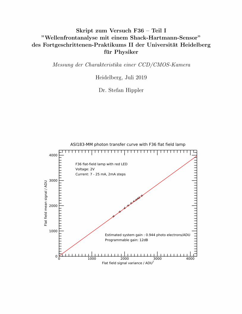
ASI183-MM photon transfer curve with F36 flat field lamp
Estimated system gain : 0.944 photo electrons/ADUProgrammable gain: 12dB
F36 flat-field lamp with red LEDVoltage: 2VCurrent: 7 - 25 mA, 2mA steps
0 1000 2000 3000 4000Flat field signal variance / ADU2
0
1000
2000
3000
4000
Flat
fiel
d m
ean
sign
al /
ADU

Inhaltsverzeichnis
1 Die CCD/CMOS-Kamera des Wellenfrontsensors 1
2 Eigenschaften der CCD/CMOS-Kamera 12.1 Einfuhrung und Begriffserklarungen . . . . . . . . . . . . . . . . . . . . . . . . . . . . . . . . 1
3 Zu bestimmende Charakteristika der CMOS Kamera 33.1 Kamera-Verstarkung (system gain) . . . . . . . . . . . . . . . . . . . . . . . . . . . . . . . . . 33.2 Kurzanleitung zur Aufnahme der Photonen-Transferkurve . . . . . . . . . . . . . . . . . . . . 3
4 Software zum Auslesen und Betreiben der CMOS-Kamera 4
A Anhang A - SONY Product Information IMX183CLK 5
B Anhang B - ZWO ASI183 Manual 12
C Anhang C - Measuring the Gain of a CCD Camera 34
i
1 Die CCD/CMOS-Kamera des Wellenfrontsensors
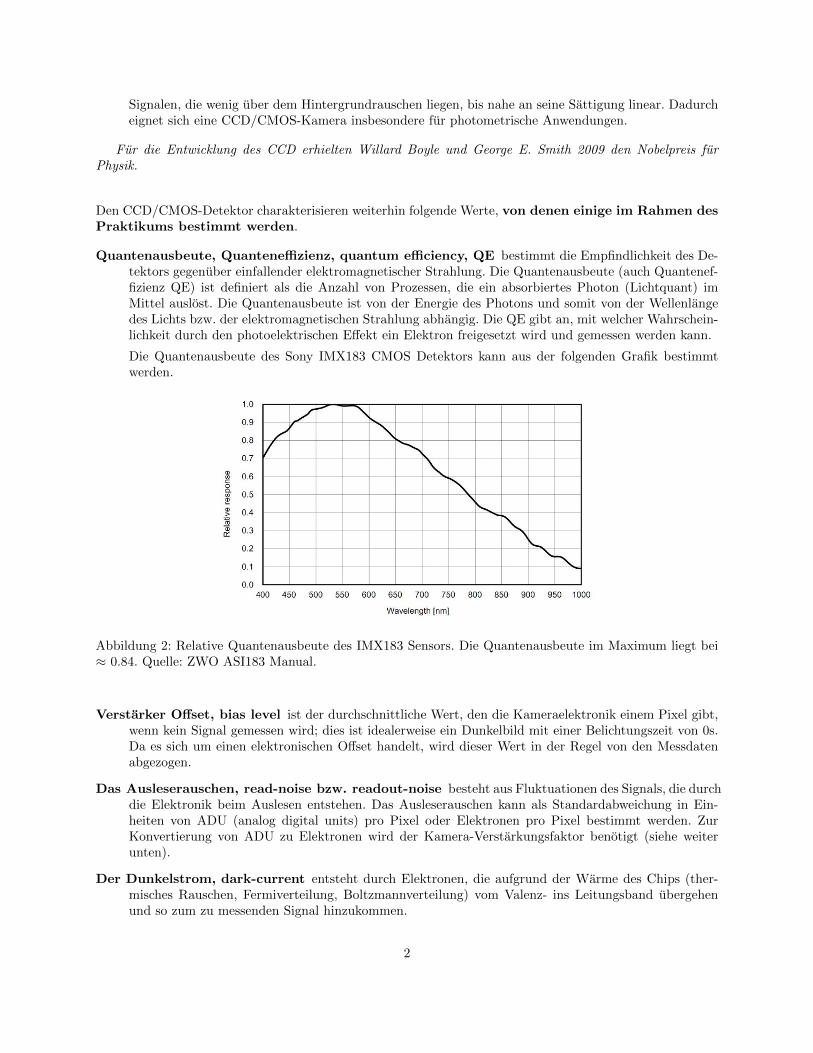
Der im Versuch aufzubauende Shack-Hartmann Wellenfrontsensor besitzt als zentrales optisches Elementeine Mikrolinsenmaske (Linsenarray).
37STERNE UND WELTRAUM Oktober 2004
ein Gitter von Punktbildern erzeugen (Abb. 8). Die laterale Verschiebung dieser Punktbilder misst lokale Wellenfrontnei-gungen über den Flächen der Mikrolin-sen. Sie wird auf vorher bestimmte Re-ferenzpositionen bezogen, welche einer perfekt ebenen Welle entsprechen. Aus den lokalen Neigungen, mathematisch gesehen also den ersten Ableitungen der Wellenfront, lässt sich dann der Wellen-frontfehler bestimmen.
Die einzelnen Mikrolinsen des Gitters messen typischerweise einen Millime-ter (Abb. 9), die Positionen der Punktbil-der werden mit CCD-Kameras gemessen. Modernste CCDs für die Adaptive Optik besitzen bis zu 128 Pixel 128 Pixel und lassen sich 2000-Mal pro Sekunde ausle-sen.
Der Curvature-WellenfrontsensorDer erste Curvature (= Krümmungs)-Wel-lenfront-Sensor (CWS) wurde Anfang der neunziger Jahre von Francois Roddier an der University of Hawaii entwickelt. Dank seiner exzellenten Leistungsfähig-keit, insbesondere in AO-Systemen mit wenigen Korrekturelementen, wurde der CWS schnell so populär wie der SHS. Die Idee des CWS besteht darin, die Intensi-tätsverteilung in zwei Ebenen zu messen, einmal vor dem Fokus und einmal nach dem Fokus. Die Differenz beider Bilder ist ein Maß für die Krümmung der Wellen-front, mathematisch betrachtet ihre zwei-te Ableitung. Das Prinzip ist in Abb. 10
schematisch dargestellt. Die in den beiden Ebenen A und B gemessenen Intensitäten kann man sich als defokussierte Bilder der Teleskop-Pupille vorstellen. Eine ge-störte, gekrümmte Wellenfront führt zu einer erhöhten Intensität in A und zu ei-ner verringerten Intensität in B. Aus dem lokalen Kontrast in den beiden Bildern er-gibt sich die Krümmung der Wellenfront. An den Rändern lässt sich die Verkippung (Engl. tilt) der Wellenfront bestimmen.
Der Abstand der beiden Messebenen Aund B von der Fokalebene ist ein wichtiger Parameter des CWS, um auf unterschied-liche Seeing-Bedingungen sowie Hellig-keit und Winkeldurchmesser der Refe-renzquelle Rücksicht zu nehmen. Dieser Parameter wird oft auch optische Verstär-kung (optical gain) genannt. Je kleiner der Abstand der Messebenen zum Fokus ist, desto geringer ist das Rauschen des CWS. Gleichzeitig wird jedoch der dynamische Messbereich verkleinert. Man kann somit den CWS im laufenden Betrieb an die je-weiligen Bedingungen anpassen.
Der CWS besteht in der Regel aus ei-nem Mikrolinsen-Array, von dem opti-sche Glasfasern das Licht direkt auf Pho-todioden (sogenannte Avalanche Photo Diodes, APD) lenken. Die Empfindlich-keit heutiger APDs ähnelt derjenigen von CCDs. Jedoch haben APDs einen entscheidenden Vorteil: Es gibt bei ih-nen kein Ausleserauschen. Damit sind sie auch bei sehr hohen Ausleseraten im Kilohertz-Bereich bestens einsetzbar. Die
Dy
Dx
CCD-Kamera Linsenraster Wellenfront Abb.: Messprinzip des Shack-Hartmann-Wellenfrontsensors (SHS). Die einfallende, durch die Atmosphäre gestörte Lichtwelle wird von einem Mikrolinsenarray in kleinere Flächen zerlegt. Jede Mikrolinse erzeugt ein Bild, des-sen Zentrum entsprechend der Neigung der Wellenfront über der Mikrolinse gegenüber einer Refe-renzposition verschoben ist.
BA
Fokus
Abb. 10: Messprinzip des Curva-ture-Wellenfront-Sensors (CWS). Eine lokal gekrümmte Lichtwelle erzeugt in der Ebene A eine hö-here Intensität als in Ebene B. Im hier gezeigten Beispiel liegt der Fokus der gestörten Licht-welle vor dem Teleskopfokus. Der Wellenfrontfehler erscheint als Intensitätsdifferenz der beiden Bilder A–B.
S24-43-ok.indd 37 3.9.2004 12:08:15 Uhr
Abbildung 1: Auf eine Mikrolinsenmaske fallende, nicht-planare Wellenfront fuhrt zu einer Verschiebung desLichtpunktes auf dem CCD/CMOS Detektor. Quelle Sterne & Weltraum Oktober 2004.
Zur Aufnahme der Punkte, die das Linsenarray in seiner Fokalebene erzeugt (siehe Abbildung 1), wirdeine CMOS-Kamera des Typs ZWO ASI183 MM benutzt. Diese hat einen IMX183CLK CMOS-Detektor derFirma Sony mit 5640 x 3694 aktiven Pixeln. Jedes Pixel hat eine Grose von 2.40 x 2.40 µm.
Weitere Daten/Spezifikationen der Kamera und des darin eingebauten Detektors sind in den Dokumentenim Anhang.
2 Eigenschaften der CCD/CMOS-Kamera
2.1 Einfuhrung und Begriffserklarungen
Unter einer CCD Kamera versteht man in der Regel eine Kamera welche mit einem CCD (charge-coupleddevice) Detektor bestuckt ist. Eine CMOS Kamera oder CMOS Sensor ist ein Bilddetektor mit aktiven Pixeln,d.h. jedes Pixel ist ein Photonendetektor mit aktivem Verstarker. Die Oberkategorie solcher Sensoren wirdoft auch als Active Pixel Sensor (APS) bezeichnet. Der hier verwendete Chip der Firma Sony wird in derComplementary metal-oxide-semiconductor Technik hergestellt, daher der Name CMOS.
Eine CCD/CMOS-Kamera zeichnet sich gegenuber anderen optischen Detektoren, wie Auge, Film oderPhoto-Multiplier, durch zwei Eigenschaften besonders aus:
Hervorragende Empfindlichkeit Die Quanteneffizienz QE liegt um die 50% - bei manchen Wellenlangensogar bis zu 90% - und ist somit um eine Großenordnung groß als beim Auge oder beim Film, wo dieQE nur einige Prozent betragt.
Linearitat zwischen Messsignal und aufgefangener Lichtmenge Anders als bei Photoplatten, dienur uber einen verhaltnismaßig kleinen Bereich linear reagieren, ist der CCD/CMOS-Detektor von
1
Signalen, die wenig uber dem Hintergrundrauschen liegen, bis nahe an seine Sattigung linear. Dadurcheignet sich eine CCD/CMOS-Kamera insbesondere fur photometrische Anwendungen.
Fur die Entwicklung des CCD erhielten Willard Boyle und George E. Smith 2009 den Nobelpreis furPhysik.
Den CCD/CMOS-Detektor charakterisieren weiterhin folgende Werte, von denen einige im Rahmen desPraktikums bestimmt werden.
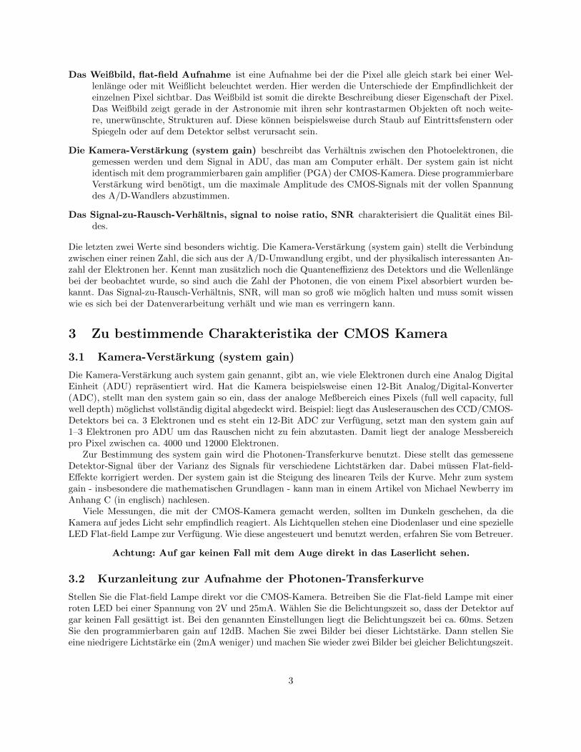
Quantenausbeute, Quanteneffizienz, quantum efficiency, QE bestimmt die Empfindlichkeit des De-tektors gegenuber einfallender elektromagnetischer Strahlung. Die Quantenausbeute (auch Quantenef-fizienz QE) ist definiert als die Anzahl von Prozessen, die ein absorbiertes Photon (Lichtquant) imMittel auslost. Die Quantenausbeute ist von der Energie des Photons und somit von der Wellenlangedes Lichts bzw. der elektromagnetischen Strahlung abhangig. Die QE gibt an, mit welcher Wahrschein-lichkeit durch den photoelektrischen Effekt ein Elektron freigesetzt wird und gemessen werden kann.
Die Quantenausbeute des Sony IMX183 CMOS Detektors kann aus der folgenden Grafik bestimmtwerden.
Abbildung 2: Relative Quantenausbeute des IMX183 Sensors. Die Quantenausbeute im Maximum liegt bei≈ 0.84. Quelle: ZWO ASI183 Manual.
Verstarker Offset, bias level ist der durchschnittliche Wert, den die Kameraelektronik einem Pixel gibt,wenn kein Signal gemessen wird; dies ist idealerweise ein Dunkelbild mit einer Belichtungszeit von 0s.Da es sich um einen elektronischen Offset handelt, wird dieser Wert in der Regel von den Messdatenabgezogen.
Das Ausleserauschen, read-noise bzw. readout-noise besteht aus Fluktuationen des Signals, die durchdie Elektronik beim Auslesen entstehen. Das Ausleserauschen kann als Standardabweichung in Ein-heiten von ADU (analog digital units) pro Pixel oder Elektronen pro Pixel bestimmt werden. ZurKonvertierung von ADU zu Elektronen wird der Kamera-Verstarkungsfaktor benotigt (siehe weiterunten).
Der Dunkelstrom, dark-current entsteht durch Elektronen, die aufgrund der Warme des Chips (ther-misches Rauschen, Fermiverteilung, Boltzmannverteilung) vom Valenz- ins Leitungsband ubergehenund so zum zu messenden Signal hinzukommen.
2
Das Weißbild, flat-field Aufnahme ist eine Aufnahme bei der die Pixel alle gleich stark bei einer Wel-lenlange oder mit Weißlicht beleuchtet werden. Hier werden die Unterschiede der Empfindlichkeit dereinzelnen Pixel sichtbar. Das Weißbild ist somit die direkte Beschreibung dieser Eigenschaft der Pixel.Das Weißbild zeigt gerade in der Astronomie mit ihren sehr kontrastarmen Objekten oft noch weite-re, unerwunschte, Strukturen auf. Diese konnen beispielsweise durch Staub auf Eintrittsfenstern oderSpiegeln oder auf dem Detektor selbst verursacht sein.
Die Kamera-Verstarkung (system gain) beschreibt das Verhaltnis zwischen den Photoelektronen, diegemessen werden und dem Signal in ADU, das man am Computer erhalt. Der system gain ist nichtidentisch mit dem programmierbaren gain amplifier (PGA) der CMOS-Kamera. Diese programmierbareVerstarkung wird benotigt, um die maximale Amplitude des CMOS-Signals mit der vollen Spannungdes A/D-Wandlers abzustimmen.
Das Signal-zu-Rausch-Verhaltnis, signal to noise ratio, SNR charakterisiert die Qualitat eines Bil-des.
Die letzten zwei Werte sind besonders wichtig. Die Kamera-Verstarkung (system gain) stellt die Verbindungzwischen einer reinen Zahl, die sich aus der A/D-Umwandlung ergibt, und der physikalisch interessanten An-zahl der Elektronen her. Kennt man zusatzlich noch die Quanteneffizienz des Detektors und die Wellenlangebei der beobachtet wurde, so sind auch die Zahl der Photonen, die von einem Pixel absorbiert wurden be-kannt. Das Signal-zu-Rausch-Verhaltnis, SNR, will man so groß wie moglich halten und muss somit wissenwie es sich bei der Datenverarbeitung verhalt und wie man es verringern kann.
3 Zu bestimmende Charakteristika der CMOS Kamera
3.1 Kamera-Verstarkung (system gain)
Die Kamera-Verstarkung auch system gain genannt, gibt an, wie viele Elektronen durch eine Analog DigitalEinheit (ADU) reprasentiert wird. Hat die Kamera beispielsweise einen 12-Bit Analog/Digital-Konverter(ADC), stellt man den system gain so ein, dass der analoge Meßbereich eines Pixels (full well capacity, fullwell depth) moglichst vollstandig digital abgedeckt wird. Beispiel: liegt das Ausleserauschen des CCD/CMOS-Detektors bei ca. 3 Elektronen und es steht ein 12-Bit ADC zur Verfugung, setzt man den system gain auf1–3 Elektronen pro ADU um das Rauschen nicht zu fein abzutasten. Damit liegt der analoge Messbereichpro Pixel zwischen ca. 4000 und 12000 Elektronen.
Zur Bestimmung des system gain wird die Photonen-Transferkurve benutzt. Diese stellt das gemesseneDetektor-Signal uber der Varianz des Signals fur verschiedene Lichtstarken dar. Dabei mussen Flat-field-Effekte korrigiert werden. Der system gain ist die Steigung des linearen Teils der Kurve. Mehr zum systemgain - insbesondere die mathematischen Grundlagen - kann man in einem Artikel von Michael Newberry imAnhang C (in englisch) nachlesen.
Viele Messungen, die mit der CMOS-Kamera gemacht werden, sollten im Dunkeln geschehen, da dieKamera auf jedes Licht sehr empfindlich reagiert. Als Lichtquellen stehen eine Diodenlaser und eine spezielleLED Flat-field Lampe zur Verfugung. Wie diese angesteuert und benutzt werden, erfahren Sie vom Betreuer.
Achtung: Auf gar keinen Fall mit dem Auge direkt in das Laserlicht sehen.
3.2 Kurzanleitung zur Aufnahme der Photonen-Transferkurve
Stellen Sie die Flat-field Lampe direkt vor die CMOS-Kamera. Betreiben Sie die Flat-field Lampe mit einerroten LED bei einer Spannung von 2V und 25mA. Wahlen Sie die Belichtungszeit so, dass der Detektor aufgar keinen Fall gesattigt ist. Bei den genannten Einstellungen liegt die Belichtungszeit bei ca. 60ms. SetzenSie den programmierbaren gain auf 12dB. Machen Sie zwei Bilder bei dieser Lichtstarke. Dann stellen Sieeine niedrigere Lichtstarke ein (2mA weniger) und machen Sie wieder zwei Bilder bei gleicher Belichtungszeit.
3

Wiederholen Sie das so oft und mit so gewahlten Lichtstarken, dass man in der Photonentransferkurve spaterdie Sattigung, die Linearitat des Poissonrauschen und den Effekt des Systemrauschens erkennen kann.
Bezeichnen Sie jeweils die Paare der Aufnahmen mit gleicher Lichtstarke als Bild A und B.
Uberlegen Sie vorher, ob eine Dunkelstrom und Offset-Korrektur zu berucksichtigen sind.
Nehmen Sie nun jedes Bild - oder einen Bereich der gleichmassig beleuchtet aussieht - und bilden sie vonjedem Bild dort das Mittel <S>. Korrigieren Sie Abweichungen zwischen den Bilderpaaren im mittlerenSignal, indem Sie jeweils das Bild B mit dem Verhaltnis <S(A)> / <S(B)> multiplizieren. Subtrahieren SieB von A. Welche Effekte fallen hier heraus? Was ist die Varianz des entstandenen Bild? Erstellen Sie diePhotonentransferkurve, d.h. tragen Sie die ermittelten Mittelwerte gegen die Varianz auf. Berechnen Sie densystem gain in Elektronen pro ADU. Erklaren Sie, falls vorhanden, die nicht-linearen Teile der Kurve. GebenSie jetzt alle Werte, die Sie bis hierhin in ADU gemessen haben, in Anzahl der Elektronen an.
4 Software zum Auslesen und Betreiben der CMOS-Kamera
Die Kamera kann mit verschiedenen Programmen betrieben werden. Das Programm des Kameraherstellersheißt asicap. Es wird uber die Kommandozeile gestartet, die Bedienung erfolgt uber das GUI. Eine weitereMethode die Kamera auszulesen basiert auf der open source software INDI (https://indilib.org). In Kom-bination mit einem python interface konnen python3 Skripte zum Auslesen benutzt werden. Beispielskriptefinden sich im Verzeichnis F36examples.
4

A Anhang A - SONY Product Information IMX183CLK

1 Copyright 2018 Sony Semiconductor Solutions Corporation
[Product Information] Ver.1.0 IMX183CLK Diagonal 15.86 mm (Type 1) CMOS Image Sensor with Square Pixel for Monochrome Cameras Description
The IMX183CLK is a diagonal 15.86 mm (Type 1) CMOS image sensor with a monochrome square pixel array and approximately 20.48 M effective pixels. 12-bit digital output makes it possible to output the signals of approximately 20.48 M effective pixels with high definition for shooting still picture. In addition, this sensor enables output effective approximately 9.03 M effective pixels (aspect ratio approx.17:9) signal performed horizontal and vertical cropping at 59.94 frame/s in 10-bit digital output format for high-definition moving picture. Furthermore, it realizes 12-bit digital output for shooting high-speed and high-definition moving pictures by horizontal and vertical addition and subsampling. Realizing high-sensitivity, low dark current, this sensor also has an electronic shutter function with variable storage time. In addition, this product is designed for use in consumer use digital still camera and consumer use camcorder. When using this for another application, Sony Semiconductor Solutions Corporation does not guarantee the quality and reliability of product. Therefore, don't use this for applications other than consumer use digital still camera and consumer use camcorder. In addition, individual specification change cannot be supported because this is a standard product. Consult your Sony Semiconductor Solutions Corporation sales representative if you have any questions.
Features
◆ Input clock frequency 72 MHz
◆All-pixel scan mode
Various readout modes (*)
◆ High-sensitivity, low dark current, no smear, excellent anti-blooming characteristics
◆ Variable-speed shutter function (minimum unit: 1 horizontal sync signal period (1XHS))
◆ Low power consumption
◆ H driver, V driver and serial communication circuit on chip
◆ CDS/PGA on chip. Gain +27 dB (step pitch 0.1 dB)
◆ 9-bit/10-bit/12-bit A/D conversion on chip
◆ All-pixel simultaneous reset supported (use with mechanical shutter)
◆ 118-pin high-precision ceramic package
* Please refer to the datasheet for binning/subsampling details of readout modes.
Sony reserves the right to change products and specifications without prior notice. Sony logo is a registered trademark of Sony Corporation.
IMX183CLK
2 Copyright 2018 Sony Semiconductor Solutions Corporation
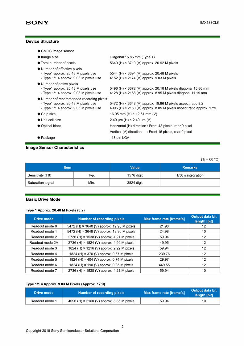
Device Structure
◆ CMOS image sensor
◆ Image size Diagonal 15.86 mm (Type 1)
◆ Total number of pixels 5640 (H) × 3710 (V) approx. 20.92 M pixels
◆ Number of effective pixels - Type1 approx. 20.48 M pixels use 5544 (H) × 3694 (V) approx. 20.48 M pixels - Type 1/1.4 approx. 9.03 M pixels use 4152 (H) × 2174 (V) approx. 9.03 M pixels
◆ Number of active pixels - Type1 approx. 20.48 M pixels use 5496 (H) × 3672 (V) approx. 20.18 M pixels diagonal 15.86 mm - Type 1/1.4 approx. 9.03 M pixels use 4128 (H) × 2168 (V) approx. 8.95 M pixels diagonal 11.19 mm
◆ Number of recommended recording pixels - Type1 approx. 20.48 M pixels use 5472 (H) × 3648 (V) approx. 19.96 M pixels aspect ratio 3:2 - Type 1/1.4 approx. 9.03 M pixels use 4096 (H) × 2160 (V) approx. 8.85 M pixels aspect ratio approx. 17:9
◆ Chip size 16.05 mm (H) × 12.61 mm (V)
◆ Unit cell size 2.40 μm (H) × 2.40 μm (V) ◆ Optical black Horizontal (H) direction : Front 48 pixels, rear 0 pixel
Vertical (V) direction : Front 16 pixels, rear 0 pixel
◆ Package 118 pin LGA
Image Sensor Characteristics
(Tj = 60 °C)
Item Value Remarks
Sensitivity (F8) Typ. 1576 digit 1/30 s integration
Saturation signal Min. 3824 digit
Basic Drive Mode
Type 1 Approx. 20.48 M Pixels (3:2)
Drive mode Number of recording pixels Max frame rate [frame/s] Output data bit length [bit]
Readout mode 0 5472 (H) × 3648 (V) approx. 19.96 M pixels 21.98 12 Readout mode 1 5472 (H) × 3648 (V) approx. 19.96 M pixels 24.98 10 Readout mode 2 2736 (H) × 1538 (V) approx. 4.21 M pixels 59.94 12
Readout mode 2A 2736 (H) × 1824 (V) approx. 4.99 M pixels 49.95 12 Readout mode 3 1824 (H) × 1216 (V) approx. 2.22 M pixels 59.94 12 Readout mode 4 1824 (H) × 370 (V) approx. 0.67 M pixels 239.76 12 Readout mode 5 1824 (H) × 404 (V) approx. 0.74 M pixels 29.97 12 Readout mode 6 1824 (H) × 190 (V) approx. 0.35 M pixels 449.55 12 Readout mode 7 2736 (H) × 1538 (V) approx. 4.21 M pixels 59.94 10
Type 1/1.4 Approx. 9.03 M Pixels (Approx. 17:9)
Drive mode Number of recording pixels Max frame rate [frame/s] Output data bit length [bit]
Readout mode 1 4096 (H) × 2160 (V) approx. 8.85 M pixels 59.94 10

B Anhang B - ZWO ASI183 Manual

ASI183 Manual
Revision 1.1
Mar, 2018 All material in this publication is subject to change without notice and its copyright totally belongs to Suzhou ZWO CO.,LTD.

ASI183 Manual
2
Table of Contents
ASI183 Manual ............................................................................................................................... 1
1. Instruction ................................................................................................................................. 3
2. Camera Models and Sensor Type ............................................................................................. 4
3. What's in the box? ..................................................................................................................... 5
4. Camera technical specifications ................................................................................................ 6
5. QE Graph & Read Noise ........................................................................................................... 7
6. Getting to know your camera .................................................................................................... 9
6.1 External View ...................................................................................................................... 9
6.2 Power consumption ........................................................................................................... 10
6.3 Cooling system .................................................................................................................. 11
6.4 Back focus distance ........................................................................................................... 11
6.5 Protect Window ................................................................................................................. 11
6.6 Analog to Digital Converter (ADC) .................................................................................. 12
6.7 Binning .............................................................................................................................. 12
6.8 DDR Buffer ....................................................................................................................... 12
7. How to use your camera.......................................................................................................... 13
8. Cleaning .................................................................................................................................. 19
9. Mechanical drawing ................................................................................................................ 20
10. Servicing ................................................................................................................................. 21
11. Warranty ................................................................................................................................. 21

ASI183 Manual
3
1. Instruction
Congratulations and thank you for buying one of our ASI Cameras!This manual will give
you a brief introduction to your ASI camera. Please take the time to read it thoroughly and if you
have any other questions, feel free to contact us. [email protected]
ASI183 Cameras are designed for astronomical photography. This is another great camera
from ZWO not only suitable for DSO imaging but also planetary imaging. The excellent
performance and multifunctional usage will impress you a lot!
For software installation instructions and other technical information please refer to “ASI
USB3.0 Cameras software Manual”
https://astronomy-imaging-camera.com/
ASI183 Manual
4
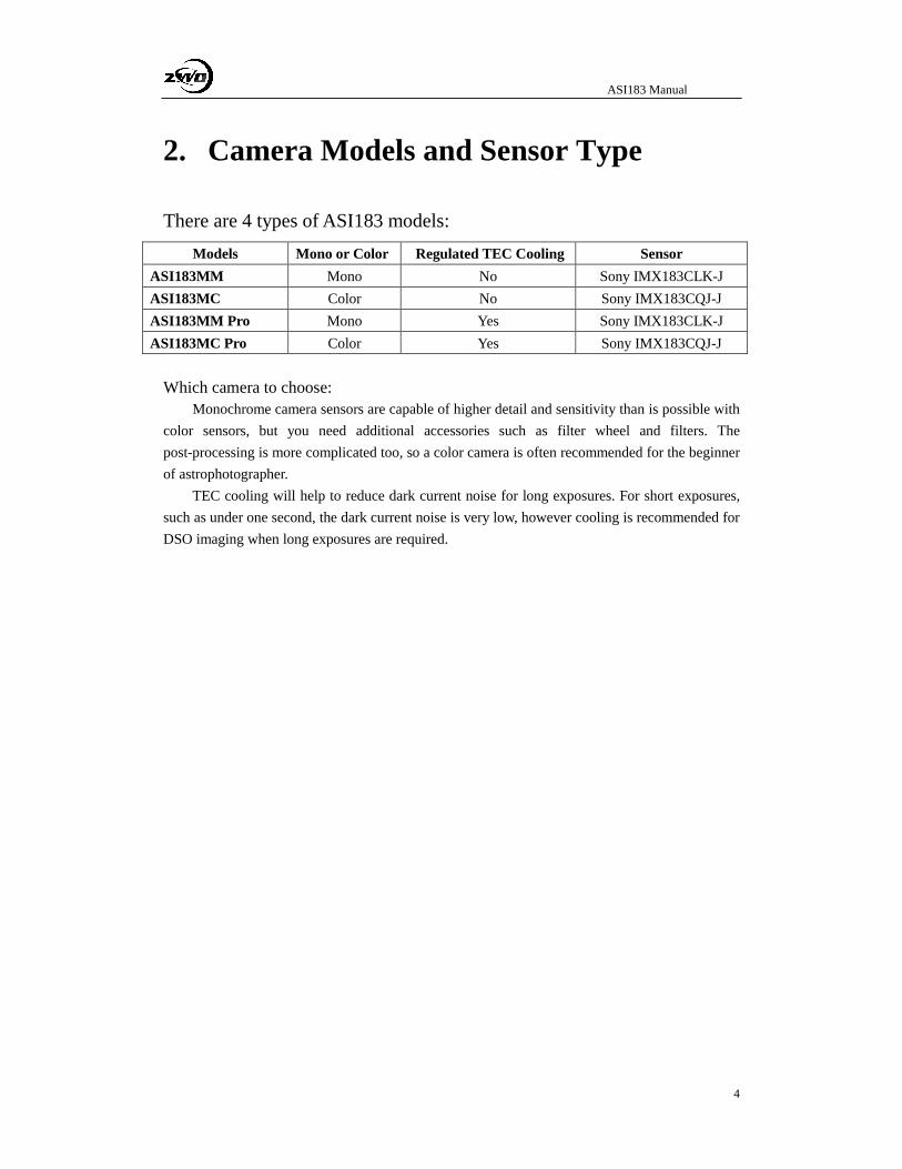
2. Camera Models and Sensor Type
There are 4 types of ASI183 models:
Models Mono or Color Regulated TEC Cooling Sensor
ASI183MM Mono No Sony IMX183CLK-J
ASI183MC Color No Sony IMX183CQJ-J
ASI183MM Pro Mono Yes Sony IMX183CLK-J
ASI183MC Pro Color Yes Sony IMX183CQJ-J
Which camera to choose:
Monochrome camera sensors are capable of higher detail and sensitivity than is possible with
color sensors, but you need additional accessories such as filter wheel and filters. The
post-processing is more complicated too, so a color camera is often recommended for the beginner
of astrophotographer.
TEC cooling will help to reduce dark current noise for long exposures. For short exposures,
such as under one second, the dark current noise is very low, however cooling is recommended for
DSO imaging when long exposures are required.
ASI183 Manual
5
3. What's in the box?
ASI183MM or ASI183MC
ASI183MM Pro or ASI183MC Pro
ASI183 Manual
6
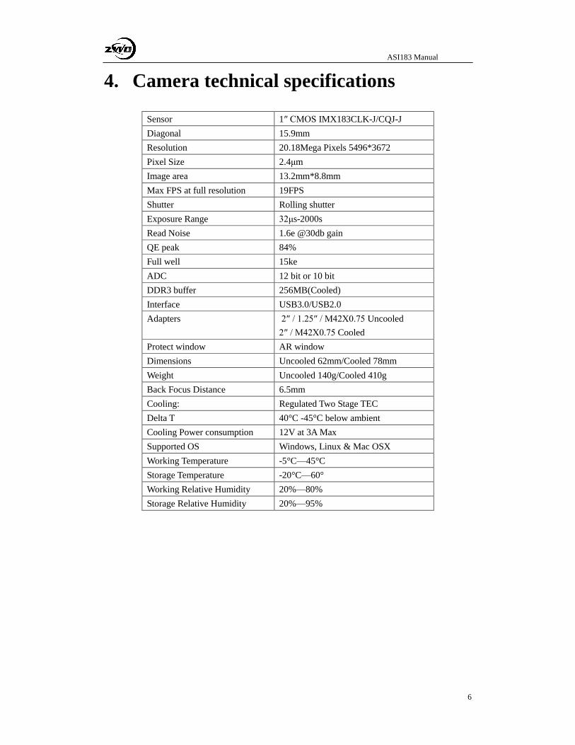
4. Camera technical specifications
Sensor 1″ CMOS IMX183CLK-J/CQJ-J
Diagonal 15.9mm
Resolution 20.18Mega Pixels 5496*3672
Pixel Size 2.4μm
Image area 13.2mm*8.8mm
Max FPS at full resolution 19FPS
Shutter Rolling shutter
Exposure Range 32μs-2000s
Read Noise 1.6e @30db gain
QE peak 84%
Full well 15ke
ADC 12 bit or 10 bit
DDR3 buffer 256MB(Cooled)
Interface USB3.0/USB2.0
Adapters 2″ / 1.25″ / M42X0.75 Uncooled
2″ / M42X0.75 Cooled
Protect window AR window
Dimensions Uncooled 62mm/Cooled 78mm
Weight Uncooled 140g/Cooled 410g
Back Focus Distance 6.5mm
Cooling: Regulated Two Stage TEC
Delta T 40°C -45°C below ambient
Cooling Power consumption 12V at 3A Max
Supported OS Windows, Linux & Mac OSX
Working Temperature -5°C—45°C
Storage Temperature -20°C—60°
Working Relative Humidity 20%—80%
Storage Relative Humidity 20%—95%

ASI183 Manual
7
5. QE Graph & Read Noise
QE and Read noise are the most important parts to measure the performance of a camera.
Higher QE and Lower read noise are needed to improve the SNR of an image.
For the Mono 183 Sensor, the peak value for QE is around 84%
Relative QE
Color 183 sensor
ASI183 Manual
8
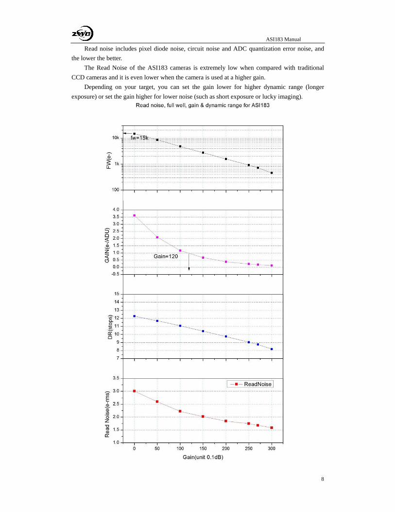
Read noise includes pixel diode noise, circuit noise and ADC quantization error noise, and
the lower the better.
The Read Noise of the ASI183 cameras is extremely low when compared with traditional
CCD cameras and it is even lower when the camera is used at a higher gain.
Depending on your target, you can set the gain lower for higher dynamic range (longer
exposure) or set the gain higher for lower noise (such as short exposure or lucky imaging).

ASI183 Manual
9
6. Getting to know your camera
6.1 External View
*
The first generation of cooled camera we used a ST4 port instead of USB2.0 hub
T2 extender ring:
2” diameters
T2 screws inside
11mm thickness
Can be removed
Protect and sealed window
AR coated D32*2mm
Heat Sink
USB2.0 Hub* USB3.0 or USB2.0 IN
Cooler power supply
5.5*2.1 DC socket
12V 3A AC-DC power
supply suggested
Cooler Maglev fan
Only on when cooler
power supply is there
Protect and sealed window
AR coated D32*2mm
1/4” screw
You can mount to tripod
USB3.0 or USB2.0 IN
ST4 Guide Port
ASI183 Manual
10
You can order the holder ring from us or our dealer to mount the cooled camera to tripod.
There is 1/4″ screw under the holder
6.2 Power consumption
ASI cameras are designed to have very low power consumption which is around 300ma@5V.
You only need the USB cable to power up the camera. However, you will need a separate power
supply to activate the cooler. We recommend 12V at 3A or more AC-DC adapter for cooler power
supply (2.1mm*5.5mm, center positive). You may also use a battery supply from 9 to 15V to
power the cooler.
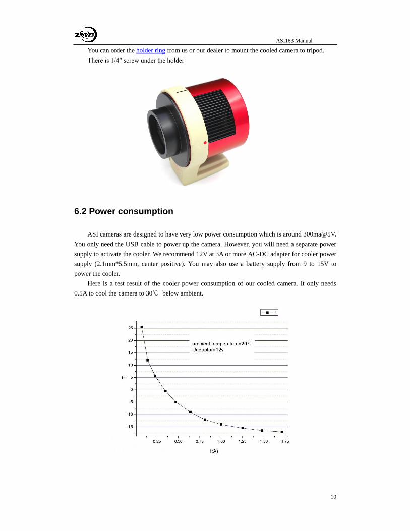
Here is a test result of the cooler power consumption of our cooled camera. It only needs
0.5A to cool the camera to 30℃ below ambient.
ASI183 Manual
11
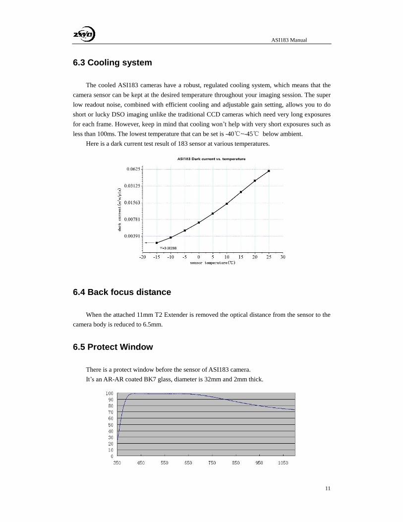
6.3 Cooling system
The cooled ASI183 cameras have a robust, regulated cooling system, which means that the
camera sensor can be kept at the desired temperature throughout your imaging session. The super
low readout noise, combined with efficient cooling and adjustable gain setting, allows you to do
short or lucky DSO imaging unlike the traditional CCD cameras which need very long exposures
for each frame. However, keep in mind that cooling won’t help with very short exposures such as
less than 100ms. The lowest temperature that can be set is -40℃~-45℃ below ambient.
Here is a dark current test result of 183 sensor at various temperatures.
6.4 Back focus distance
When the attached 11mm T2 Extender is removed the optical distance from the sensor to the
camera body is reduced to 6.5mm.
6.5 Protect Window
There is a protect window before the sensor of ASI183 camera.
It’s an AR-AR coated BK7 glass, diameter is 32mm and 2mm thick.
ASI183 Manual
12
6.6 Analog to Digital Converter (ADC)
The ASI183 camera records in 12bit ADC and 10bit ADC. You can image at a faster fps rate
if you choose to use 10bit ADC (high speed mode). This camera also supports ROI (region of
interest) shooting, and this smaller ROI has faster fps. You can uncheck “high speed” and choose
8bit output on software to enable 10bit ADC output, otherwise this camera will use 12bit ADC.
Here is the maximum speed of ASI183 running at 10bit ADC or 12bit ADC at 8bit mode.
Resolution USB3.0
10Bit ADC 12Bit ADC
5496×3672 19fps 19fps
3840x2160 41fps 36fps
1920x1680 80fps 70fps
1280x720 117fps 103fps
640x480 170fps 150fps
320x240 308.fps 271fps
6.7 Binning
The ASI183 camera supports hardware bin2 and software bin2, bin3 and bin4 mode.
Hardware binning is supported by sensor but is done in digital domain like software binning and
use 10bit ADC. The only advantage of hardware binning is faster fps. We recommend customer to
use software binning if you don’t care speed.
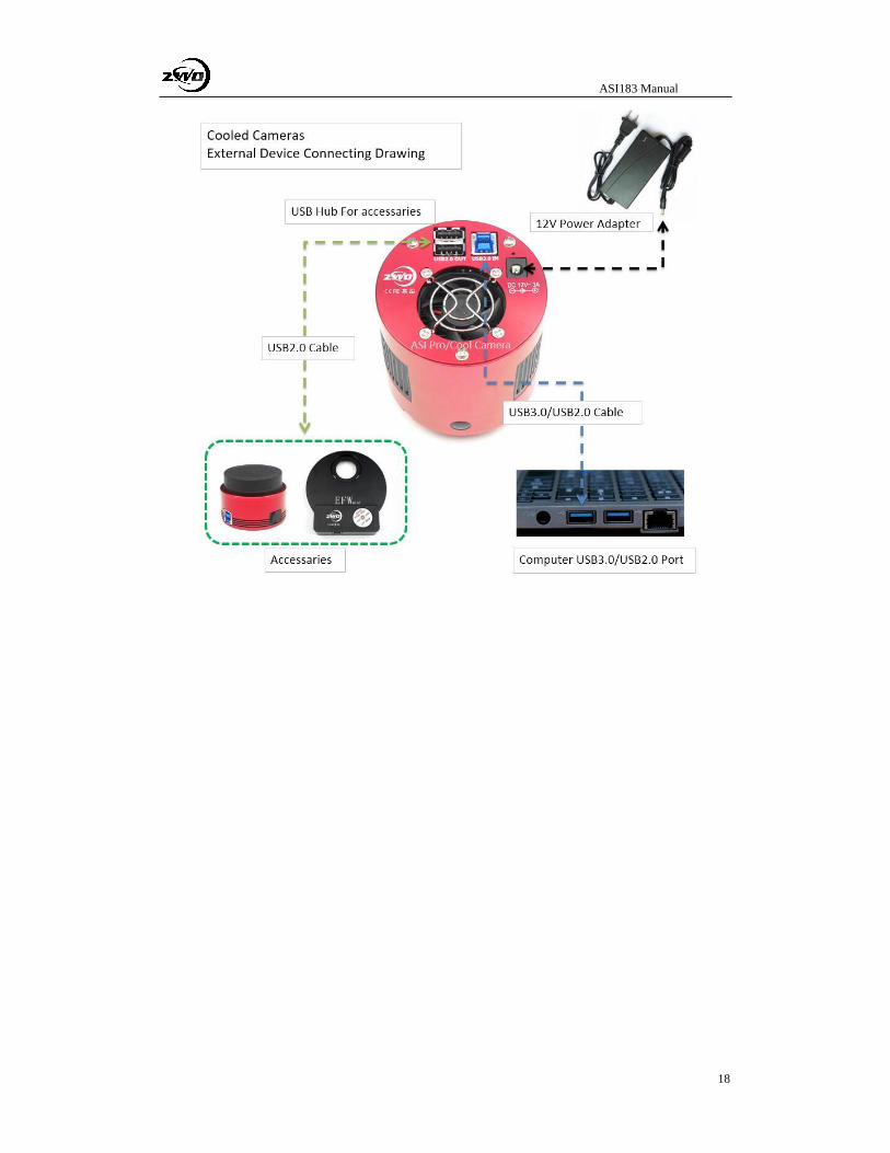
6.8 DDR Buffer
The ASI183 Pro camera includes a 256MB DDR3 memory buffer to help improve data
transfer reliability. Additionally, the use of a memory buffer minimizes amp-glow, which is caused
by the slow transfer speeds when the camera is used with a USB 2.0 port. DDR memory buffer is
the main difference between ASI “Cool” and “Pro” cameras.
ASI183 Manual
13
7. How to use your camera
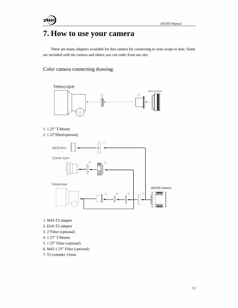
There are many adapters available for this camera for connecting to your scope or lens. Some
are included with the camera and others you can order from our site:
Color camera connecting drawing:
1. 1.25” T-Mount
2. 1.25”filter(optional)
1. M43-T2 adapter
2. EOS-T2 adapter
3. 2”Filter (optional)
4. 1.25” T-Mount
5. 1.25” Filter (optional)
6. M42-1.25” Filter (optional)
7. T2 extender 11mm
ASI183 Manual
14
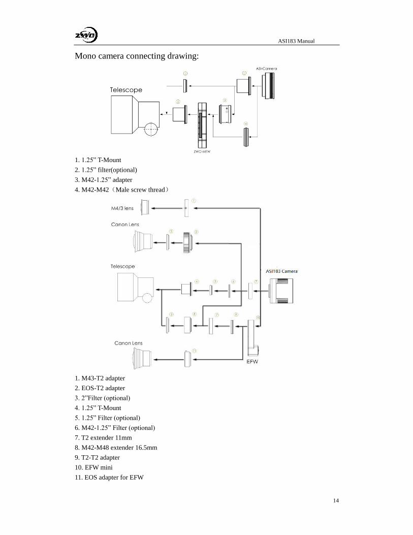
Mono camera connecting drawing:
1. 1.25” T-Mount
2. 1.25” filter(optional)
3. M42-1.25” adapter
4. M42-M42(Male screw thread)
1. M43-T2 adapter
2. EOS-T2 adapter
3. 2”Filter (optional)
4. 1.25” T-Mount
5. 1.25” Filter (optional)
6. M42-1.25” Filter (optional)
7. T2 extender 11mm
8. M42-M48 extender 16.5mm
9. T2-T2 adapter
10. EFW mini
11. EOS adapter for EFW
ASI183 Manual
15
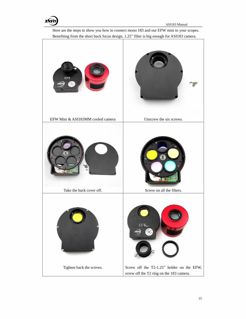
Here are the steps to show you how to connect mono 183 and our EFW mini to your scopes.
Benefiting from the short back focus design, 1.25” filter is big enough for ASI183 camera.
EFW Mini & ASI183MM cooled camera
Unscrew the six screws.
Take the back cover off.
Screw on all the filters.
Tighten back the screws.
Screw off the T2-1.25” holder on the EFW,
screw off the T2 ring on the 183 camera.
ASI183 Manual
16
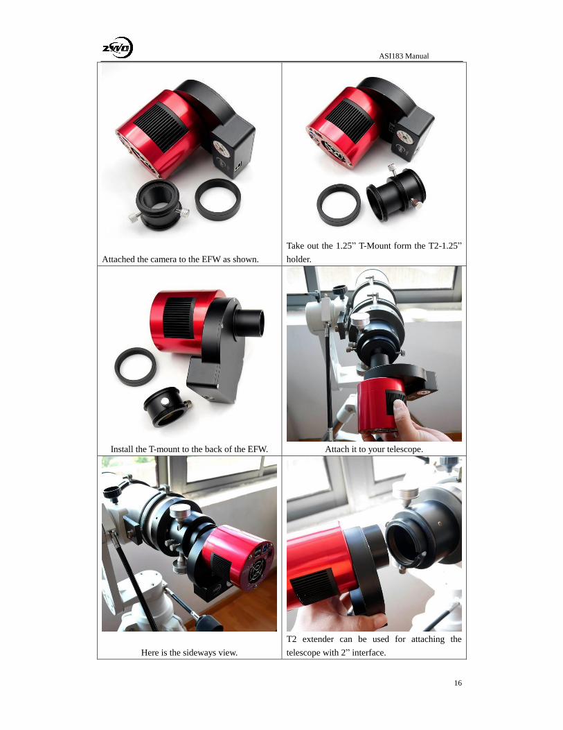
Attached the camera to the EFW as shown.
Take out the 1.25” T-Mount form the T2-1.25”
holder.
Install the T-mount to the back of the EFW.
Attach it to your telescope.
Here is the sideways view.
T2 extender can be used for attaching the
telescope with 2” interface.
ASI183 Manual
17
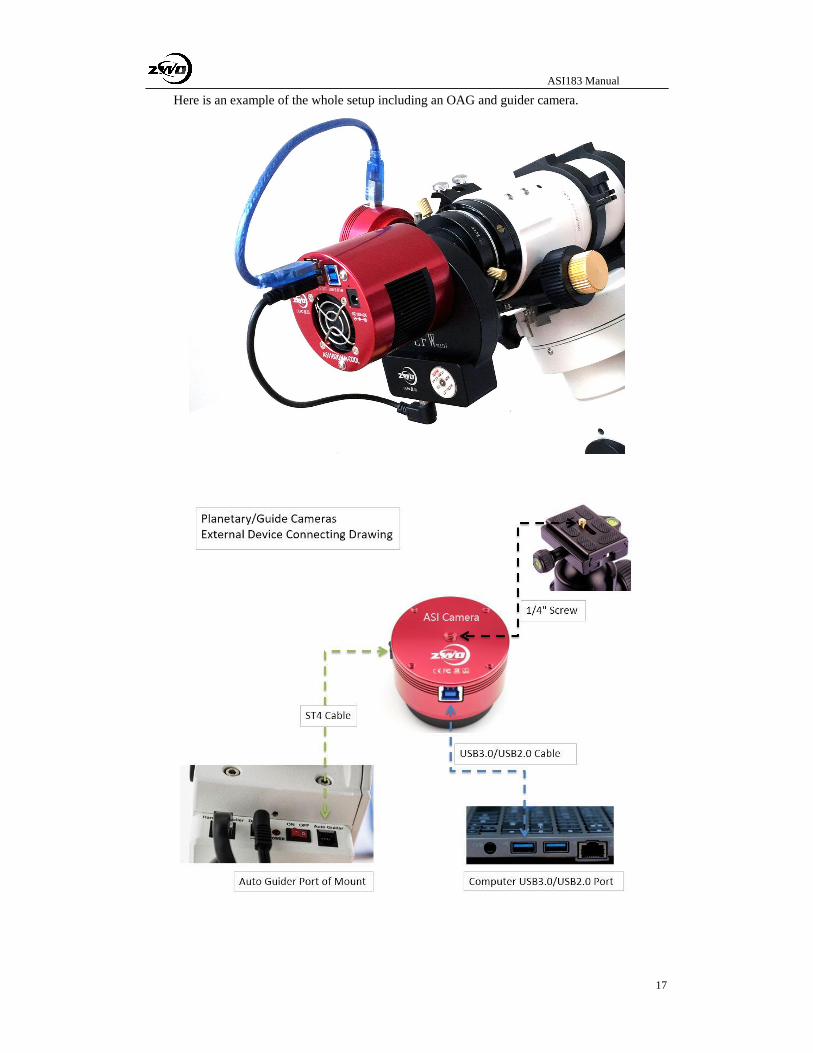
Here is an example of the whole setup including an OAG and guider camera.
ASI183 Manual
18
ASI183 Manual
19
8. Cleaning
The camera comes with an AR protect window, which can protect the sensor from dust and
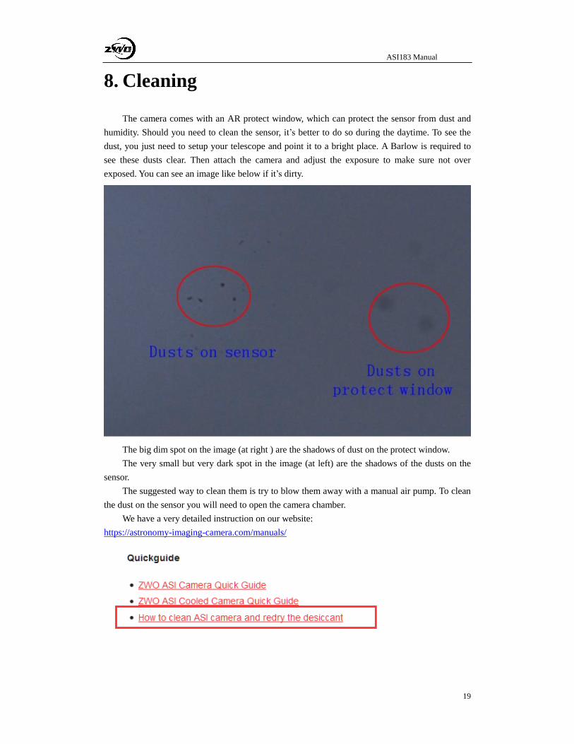
humidity. Should you need to clean the sensor, it’s better to do so during the daytime. To see the
dust, you just need to setup your telescope and point it to a bright place. A Barlow is required to
see these dusts clear. Then attach the camera and adjust the exposure to make sure not over
exposed. You can see an image like below if it’s dirty.
The big dim spot on the image (at right ) are the shadows of dust on the protect window.
The very small but very dark spot in the image (at left) are the shadows of the dusts on the
sensor.
The suggested way to clean them is try to blow them away with a manual air pump. To clean
the dust on the sensor you will need to open the camera chamber.
We have a very detailed instruction on our website:
https://astronomy-imaging-camera.com/manuals/

ASI183 Manual
20
9. Mechanical drawing
ASI183MM/ASI183MC
ASI183MM Pro /ASI183MC Pro
ASI183 Manual
21
10. Servicing
Repairs, servicing and upgrades are available by emailing [email protected]
For customers who bought the camera form your local dealer, dealer is responsible for the
customer service.
11. Warranty
We provide 2-year warranty for our products, we will offer repair service for free or replace
for free if the camera doesn’t work within warranty period.
After the warranty period, we will continue to provide repair support and service on a
charged basis.
This warranty does not apply to damage that occurred as a result of abuse or misuse, or
caused by a fall or any other transportation failures after purchase.
Customer must pay for shipping when shipping the camera back for repair or replacement.

C Anhang C - Measuring the Gain of a CCD Camera
Axiom Tech Note 1. Measuring the Gain of a CCD Camera Page 1 of 9
Copyright © 1998-2000 Axiom Research, Inc. All Rights Reserved.
Measuring the Gain of a CCD Camera
Michael Newberry Axiom Research, Inc.
Copyright © 1998-2000. All Rights Reserved.
1. Introduction
The gain of a CCD camera is the conversion between the number of electrons ("e-") recorded by the CCD and the number of digital units ("counts") contained in the CCD image. It is useful to know this conversion for evaluating the performance of the CCD camera. Since quantities in the CCD image can only be measured in units of counts, knowing the gain permits the calculation of quantities such as readout noise and full well capacity in the fundamental units of electrons. The gain value is required by some types of image de-convolution such as Maximum Entropy since, in order to do properly the statistical part of the calculation, the processing needs to convert the image into units of electrons. Calibrating the gain is also useful for detecting electronic problems in a CCD camera, including gain change at high or low signal level, and the existence of unexpected noise sources.
This Axiom Tech Note develops the mathematical theory behind the gain calculation and shows how the mathematics suggests ways to measure the gain accurately. This note does not address the issues of basic image processing or CCD camera operation, and a basic understanding of CCD bias, dark and flat field correction is assumed. Developing the mathematical background involves some algebra, and readers who do not wish to read through the algebra may wish to skip Section 3.
2. Overview
The gain value is set by the electronics that read out the CCD chip. Gain is expressed in units of electrons per count. For example, a gain of 1.8 e-/count means that the camera produces 1 count for every 1.8 recorded electrons. Of course, we cannot split electrons into fractional parts, as in the case for a gain of 1.8 e-/count. What this number means is that 4/5 of the time 1 count is produced from 2 electrons, and 1/5 of the time 1 count is produced from 1 electron. This number is an average conversion ratio, based on changing large numbers of electrons into large numbers of counts. Note: This use of the term "gain" is in the opposite sense to the way a circuit designer would use the term since, in electronic design, gain is considered to be an increase in the number of output units compared with the number of input units.
It is important to note that every measurement you make in a CCD image uses units of counts. Since one camera may use a different gain than another camera, count units do not provide a straightforward comparison to be made. For example, suppose two cameras each record 24 electrons in a certain pixel. If the gain of the first camera is 2.0 and the gain of the second camera is 8.0, the same pixel would measure 12 counts in the image from the first camera and 3 counts in the image from the second camera. Without knowing the gain, comparing 12 counts against 3 counts is pretty meaningless.
Before a camera is assembled, the manufacturer can use the nominal tolerances of the electronic components to estimate the gain to within some level of uncertainty. This calculation is based on resistor values used in the gain stage of the CCD readout electronics. However, since the actual resistance is subject to component tolerances, the gain of the assembled camera may be quite different from this estimate. The actual gain can only be determined by actual performance in a gain calibration test. In addition, manufacturers

Axiom Tech Note 1. Measuring the Gain of a CCD Camera Page 2 of 9
Copyright © 1998-2000 Axiom Research, Inc. All Rights Reserved.
sometimes do not perform an adequate gain measurement. Because of these issues, it is not unusual to find that the gain of a CCD camera differs substantially from the value quoted by the manufacturer.
3. Mathematical Background
The signal recorded by a CCD and its conversion from units of electrons to counts can be mathematically described in a straightforward way. Understanding the mathematics validates the gain calculation technique described in the next section, and it shows why simpler techniques fail to give the correct answer.
This derivation uses the concepts of "signal" and "noise". CCD performance is usually described in terms of signal to noise ratio, or "S/N", but we shall deal with them separately here. The signal is defined as the quantity of information you measure in the image— in other words, the signal is the number of electrons recorded by the CCD or the number of counts present in the CCD image. The noise is the uncertainty in the signal. Since the photons recorded by the CCD arrive in random packets (courtesy of nature), observing the same source many times records a different number of electrons every time. This variation is a random error, or "noise" that is added to the true signal. You measure the gain of the CCD by comparing the signal level to the amount of variation in the signal. This works because the relationship between counts and electrons is different for the signal and the variance. There are two ways to make this measurement:
1. Measure the signal and variation within the same region of pixels at many intensity levels.
2. Measure the signal and variation in a single pixel at many intensity levels.
Both of these methods are detailed in section 6. They have the same mathematical foundation.
To derive the relationship between signal and variance in a CCD image, let us define the following quantities:
SC The signal measured in count units in the CCD image
SE The signal recorded in electron units by the CCD chip. This quantity is unknown.
NC The total noise measured in count units in the CCD image.
NE The total noise in terms of recorded electrons. This quantity is unknown.
g The gain, in units of electrons per count. This will be calculated.
RE The readout noise of the CCD chip, measured in electrons. This quantity is unknown.
? E The photon noise in the signal NE
? o An additional noise source in the image. This is described below.
We need an equation to relate the number of electrons, which is unknown, to quantities we measure in the CCD image in units of counts. The signals and noises are simply related
Axiom Tech Note 1. Measuring the Gain of a CCD Camera Page 3 of 9
Copyright © 1998-2000 Axiom Research, Inc. All Rights Reserved.
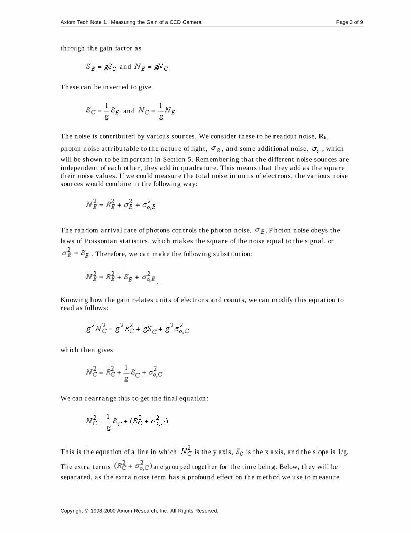
through the gain factor as
and
These can be inverted to give
and
The noise is contributed by various sources. We consider these to be readout noise, RE,
photon noise attributable to the nature of light, , and some additional noise, , which will be shown to be important in Section 5. Remembering that the different noise sources are independent of each other, they add in quadrature. This means that they add as the square their noise values. If we could measure the total noise in units of electrons, the various noise sources would combine in the following way:
The random arrival rate of photons controls the photon noise, . Photon noise obeys the laws of Poissonian statistics, which makes the square of the noise equal to the signal, or
. Therefore, we can make the following substitution:
.
Knowing how the gain relates units of electrons and counts, we can modify this equation to read as follows:
which then gives
We can rearrange this to get the final equation:
This is the equation of a line in which is the y axis, is the x axis, and the slope is 1/g.
The extra terms are grouped together for the time being. Below, they will be separated, as the extra noise term has a profound effect on the method we use to measure

Axiom Tech Note 1. Measuring the Gain of a CCD Camera Page 4 of 9
Copyright © 1998-2000 Axiom Research, Inc. All Rights Reserved.
gain. A better way to apply this equation is to plot our measurements with as the y axis
and as the x axis, as this gives the gain directly as the slope. Theoretically, at least, one
could also calculate the readout noise, , from the point where the line hits the y axis at = 0. Knowing the gain then allows this to be converted to a Readout Noise in the
standard units of electrons. However, finding the intercept of the line is not a good method, because the readout noise is a relatively small quantity and the exact path where the line passes through the y axis is subject to much uncertainty.
With the mathematics in place, we are now ready to calculate the gain. So far, I have
ignored the "extra noise term", . In the next 2 sections, I will describe the nature of the extra noise term and show how it affects the way we measure the gain of a CCD camera.
4. Crude Estimation of the Gain
In the previous section we derived the complete equation that relates the signal and the noise you measure in a CCD image. One popular method for measuring the gain is very simple, but it is not based on the full equation I have derived above. The simple can be described as follows:
1. Obtain images at different signal levels and subtract the bias from them. This is necessary because the bias level adds to the measured signal but does not contribute noise.
2. Measure the signal and noise in each image. The mean and standard deviation of a region of pixels give these quantities. Square the noise value to get a variance at each signal level.
3. For each image, plot Signal on the y axis against Variance on the x axis. 4. Find the slope of a line through the points. The gain equals the slope.
Is measuring the gain actually this simple? Well, yes and no. If we actually make the measurement over a substantial range of signal, the data points will follow a curve rather than a line. Using the present method we will always measure a slope that is too shallow, and with it we will always underestimate the gain. Using only low signal levels, this method can give a gain value that is at least "in the ballpark" of the true value. At low signal levels, the curvature is not apparent, though present. However, the data points have some amount of scatter themselves, and without a long baseline of signal, the slope might not be well determined. The curvature in the Signal - Variance plot is caused by the extra noise term which this simple method neglects.
The following factors affect the amount of curvature we obtain:
• The color of the light source. Blue light is worse because CCD’s show the greatest surface irregularity at shorter wavelengths. These irregularities are described in Section 5.
• The fabrication technology of the CCD chip. These issues determine the relative strength of the effects described in item 1.
• The uniformity of illumination on the CCD chip. If the Illumination is not uniform, then the sloping count level inside the pixel region used to measure it inflates the measured standard deviation.
Axiom Tech Note 1. Measuring the Gain of a CCD Camera Page 5 of 9
Copyright © 1998-2000 Axiom Research, Inc. All Rights Reserved.
Fortunately, we can obtain the proper value by doing just a bit more work. We need to change the experiment in a way that makes the data plot as a straight line. We have to
devise a way to account for the extra noise term, . If were a constant value we could combine it with the constant readout noise. We have not talked in detail about readout noise, but we have assumed that it merges together all constant noise sources that do not change with the signal level.
5. Origin of the Extra Noise Term in the Signal - Variance Relationship
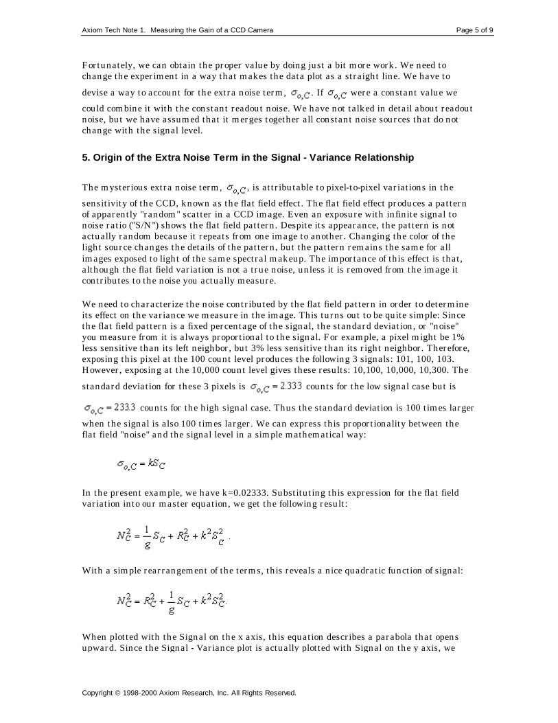
The mysterious extra noise term, , is attributable to pixel-to-pixel variations in the sensitivity of the CCD, known as the flat field effect. The flat field effect produces a pattern of apparently "random" scatter in a CCD image. Even an exposure with infinite signal to noise ratio ("S/N") shows the flat field pattern. Despite its appearance, the pattern is not actually random because it repeats from one image to another. Changing the color of the light source changes the details of the pattern, but the pattern remains the same for all images exposed to light of the same spectral makeup. The importance of this effect is that, although the flat field variation is not a true noise, unless it is removed from the image it contributes to the noise you actually measure.
We need to characterize the noise contributed by the flat field pattern in order to determine its effect on the variance we measure in the image. This turns out to be quite simple: Since the flat field pattern is a fixed percentage of the signal, the standard deviation, or "noise" you measure from it is always proportional to the signal. For example, a pixel might be 1% less sensitive than its left neighbor, but 3% less sensitive than its right neighbor. Therefore, exposing this pixel at the 100 count level produces the following 3 signals: 101, 100, 103. However, exposing at the 10,000 count level gives these results: 10,100, 10,000, 10,300. The
standard deviation for these 3 pixels is counts for the low signal case but is
counts for the high signal case. Thus the standard deviation is 100 times larger when the signal is also 100 times larger. We can express this proportionality between the flat field "noise" and the signal level in a simple mathematical way:
In the present example, we have k=0.02333. Substituting this expression for the flat field variation into our master equation, we get the following result:
With a simple rearrangement of the terms, this reveals a nice quadratic function of signal:
When plotted with the Signal on the x axis, this equation describes a parabola that opens upward. Since the Signal - Variance plot is actually plotted with Signal on the y axis, we
Axiom Tech Note 1. Measuring the Gain of a CCD Camera Page 6 of 9
Copyright © 1998-2000 Axiom Research, Inc. All Rights Reserved.
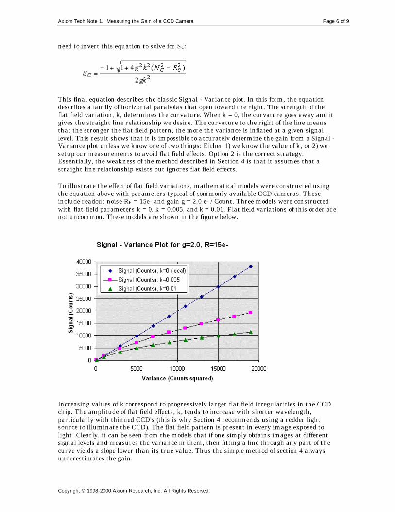
need to invert this equation to solve for SC:
This final equation describes the classic Signal - Variance plot. In this form, the equation describes a family of horizontal parabolas that open toward the right. The strength of the flat field variation, k, determines the curvature. When k = 0, the curvature goes away and it gives the straight line relationship we desire. The curvature to the right of the line means that the stronger the flat field pattern, the more the variance is inflated at a given signal level. This result shows that it is impossible to accurately determine the gain from a Signal - Variance plot unless we know one of two things: Either 1) we know the value of k, or 2) we setup our measurements to avoid flat field effects. Option 2 is the correct strategy. Essentially, the weakness of the method described in Section 4 is that it assumes that a straight line relationship exists but ignores flat field effects.
To illustrate the effect of flat field variations, mathematical models were constructed using the equation above with parameters typical of commonly available CCD cameras. These include readout noise RE = 15e- and gain g = 2.0 e- / Count. Three models were constructed with flat field parameters k = 0, k = 0.005, and k = 0.01. Flat field variations of this order are not uncommon. These models are shown in the figure below.
Increasing values of k correspond to progressively larger flat field irregularities in the CCD chip. The amplitude of flat field effects, k, tends to increase with shorter wavelength, particularly with thinned CCD's (this is why Section 4 recommends using a redder light source to illuminate the CCD). The flat field pattern is present in every image exposed to light. Clearly, it can be seen from the models that if one simply obtains images at different signal levels and measures the variance in them, then fitting a line through any part of the curve yields a slope lower than its true value. Thus the simple method of section 4 always underestimates the gain.
Axiom Tech Note 1. Measuring the Gain of a CCD Camera Page 7 of 9
Copyright © 1998-2000 Axiom Research, Inc. All Rights Reserved.
The best strategy for doing the Signal - Variance method is to find a way to produce a straight line by properly compensating for flat field effects. This is important by the "virtue of straightness": Deviation from a straight line is completely unambiguous and easy to detect. It avoids the issue of how much curvature is attributable to what cause. The electronic design of a CCD camera is quite complex, and problems can occur, such as gain change at different signal levels or unexplained extra noise at high or low signal levels. Using a "robust" method for calculating gain, any significant deviation from a line is a diagnostic of possible problems in the camera electronics. Two such methods are described in the following section.
6. Robust Methods for Measuring Gain
In previous sections, the so-called simple method of estimating the gain was shown to be an oversimplification. Specifically, it produces a Signal - Variance plot with a curved relationship resulting from flat field effects. This section presents two robust methods that correct the flat field effects in the Signal - Variance relationship to yield the desired straight-line relationship. This permits an accurate gain value to be calculated. Adjusting the method to remove flat field effects is a better strategy than either to attempt to use a low signal level where flat field effects are believed not to be important or to attempt to measure and compensate for the flat field parameter k.
When applying the robust methods described below, one must consider some procedural issues that apply to both:
• Both methods measure sets of 2 or more images at each signal level. An image set is defined as 2 or more successive images taken under the same illumination conditions. To obtain various signal levels, it is better to change the intensity received by the CCD than to change the exposure time. This may be achieved either by varying the light source intensity or by altering the amount of light passing into the camera. The illumination received by the CCD should not vary too much within a set of images, but it does not have to be truly constant.
• Cool the CCD camera to reduce the dark current to as low as possible. This prevents you from having to subtract dark frames from the images (doing so adds noise, which adversely affects the noise measurements at low signal level). In addition, if the bias varies from one frame to another, be sure to subtract a bias value from every image.
• The CCD should be illuminated the same way for all images within a set. Irregularities in illumination within a set are automatically removed by the image processing methods used in the calibration. It does not matter if the illumination pattern changes when you change the intensity level for a different image set.
• Within an image set, variation in the light intensity is corrected by normalizing the images so that they have the same average signal within the same pixel region. The process of normalizing multiplies the image by an appropriate constant value so that its mean value within the pixel region matches that of other images in the same set. Multiplying by a constant value does not affect the signal to noise ratio or the flat field structure of the image.
• Do not estimate the CCD camera's readout noise by calculating the noise value at zero signal. This is the square root of the variance where the gain line intercepts the y axis. Especially do not use this value if bias is not subtracted from every frame. To calculate the readout noise, use the "Two Bias" method and apply the gain value determined from this test. In the Two Bias Method, 2 bias frames are taken in succession and then subtracted from each other. Measure the standard deviation inside a region of, say 100x100 pixels and divide by 1.4142. This gives the readout noise in units of counts. Multiply this by the gain factor to get the Readout Noise in

Axiom Tech Note 1. Measuring the Gain of a CCD Camera Page 8 of 9
Copyright © 1998-2000 Axiom Research, Inc. All Rights Reserved.
units of electrons. If bias frames are not available, cool the camera and obtain two dark frames of minimum exposure, then apply the Two Bias Method to them.
A. METHOD 1: Correct the flat field effects at each signal level
In this strategy, the flat field effects are removed by subtracting one image from another at each signal level. Here is the recipe:
For each intensity level, do the following:
1. Obtain 2 images in succession at the same light level. Call these images A and B.
2. Subtract the bias level from both images. Keep the exposure short so that the dark current is negligibly small. If the dark current is large, you should also remove it from both frames.
3. Measure the mean signal level S in a region of pixels on images A and B. Call these mean signals SA and SB. It is best if the bounds of the region change as little as possible from one image to the next. The region might be as small as 50x50 to 100x100 pixels but should not contain obvious defects such as cosmic ray hits, dead pixels, etc.
4. Calculate the ratio of the mean signal levels as r = SA / SB. 5. Multiply image B by the number r. This corrects image B to the same signal
level as image A without affecting its noise structure or flat field variation. 6. Subtract image B from image A. The flat field effects present in both images
should be cancelled to within the random errors. 7. Measure the standard deviation over the same pixel region you used in step
3. Square this number to get the Variance. In addition, divide the resulting variance by 2.0 to correct for the fact that the variance is doubled when you subtract one similar image from another.
8. Use the Signal from step 3 and the Variance from step 7 to add a data point to your Signal - Variance plot.
9. Change the light intensity and repeat steps 1 through 8.
B. METHOD 2: Avoid flat field effects using one pixel in many images.
This strategy avoids the flat field variation by considering how a single pixel varies among many images. Since the variance is calculated from a single pixel many times, rather than from a collection of different pixels, there is no flat field variation.
To calculate the variance at a given signal level, you obtain many frames, measure the same pixel in each frame, and calculate the variance among this set of values. One problem with this method is that the variance itself is subject to random errors and is only an estimate of the true value. To obtain a reliable variance, you must use 100’s of images at each intensity level. This is completely analogous to measuring the variance over a moderate sized pixel region in Method A; in both methods, using many pixels to compute the variance gives a more statistically sound value. Another limitation of this method is that it either requires a perfectly stable light source or you have to compensate for light source variation by adjusting each image to the same average signal level before measuring its pixel. Altogether, the method requires a large number of images and a lot of processing. For this reason, Method A is preferred. In any case, here is the recipe:

Axiom Tech Note 1. Measuring the Gain of a CCD Camera Page 9 of 9
Copyright © 1998-2000 Axiom Research, Inc. All Rights Reserved.
Select a pixel to measure at the same location in every image. Always measure the same pixel in every image at every signal level.
For each intensity level, do the following:
1. Obtain at least 100 images in succession at the same light level. Call the first image A and the remaining images i. Since you are interested in a single pixel, the images may be small, of order 100x100 pixels.
2. Subtract the bias level from each image. Keep the exposure short so that the dark current is negligibly small. If the dark current is large, you should also remove it from every frame.
3. Measure the mean signal level S in a rectangular region of pixels on image A. Measure the same quantity in each of the remaining images. The measuring region might be as small as 50x50 to 100x100 pixels and should be centered on the brightest part of the image.
4. For each image Si other than the first, calculate the ratio of its mean signal level to that of image A. This gives a number for each image, ri = SA / Si.
5. Multiply each image i by the number ri. This corrects each image to the same average intensity as image A.
6. Measure the number of counts in the selected pixel in every one of the images. From these numbers, compute a mean count and standard deviation. Square the standard deviation to get the variance.
7. Use the Signal and Variance from step 6 to add a data point to your Signal - Variance plot.
8. Change the light intensity and repeat steps 1 through 7.
7. Summary
In Section 3 we derived the mathematical relationship between Signal and Variance in a CCD image. The resulting equation includes flat field effects that are later shown to weaken the validity of the gain unless they are compensated. Section 4 describes a simple, commonly employed method for estimating the gain of a CCD camera. This method does not compensate for flat field effects and can lead to large errors in the gain calculation. The weakness of this method is described and mathematically modeled in section 5. In Section 6, two methods are proscribed for eliminating the flat field problem. Method A, which removes the flat field effect by subtracting two images at each signal level requires far less image processing effort and is the preferred choice.
Skript zum Versuch F36 Teil II „Wellenfrontanalyse mit einem Shack-Hartmann-Sensor“
des Fortgeschrittenen-Praktikums II der Universität Heidelberg für Physiker
Aufbau eines Shack-Hartmann Wellenfrontsensors. Messung einfacher optischer Aberrationen. Wellenfrontrekonstruktion mit Hilfe von Zernike-Funktionen.
Heidelberg, Oktober 2006
Dr. Stefan Hippler, Dr. Wolfgang Brandner, Prof. Dr. Thomas Henning
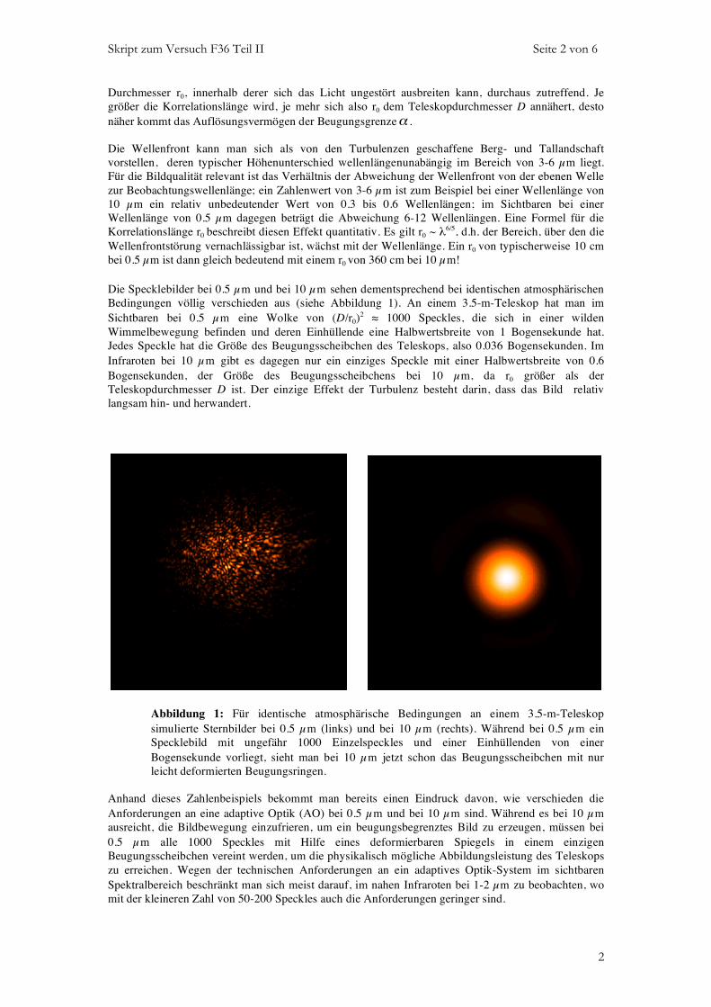
Einleitung und Motivation: Der Einfluss der Atmosphäre auf die Bildqualität eines Teleskops Betrachtet man den Sternenhimmel mit dem bloßen Auge, so fällt in erster Linie das Funkeln der Sterne, die Szintillation, auf. Dieser Effekt wird durch die atmosphärischen Turbulenzen verursacht, die dafür sorgen, dass ständig kalte und warme Luftschichten vermischt werden. Die Temperaturabhängigkeit des Brechungsindexes der Luft führt zu einer, wenn auch sehr schwachen, optischen Inhomogenität. Dadurch zerfällt die Atmosphäre in viele zufällig verteilte Turbulenzzellen mit Durchmessern von 10 bis 20 cm, die wie schwache Linsen wirken. Durch ihre lichtsammelnde Wirkung sorgen sie in Bodennähe für Intensitätsschwankungen über Bereiche von einigen Zentimetern. Beim Beobachten mit einem Teleskop von mehreren Metern Durchmesser machen sich die Turbulenzen weniger durch Intensitätsschwankungen als durch die granulationsartige Struktur (Speckles) der Bilder von Einzelsternen störend bemerkbar. Da von der Teleskopapertur viele dieser Turbulenzzellen gleichzeitig erfasst werden, zersplittert das Bild in viele zufällig verteilte Einzelbilder, die Speckles. Die Zahl der Speckles entspricht ungefähr der Anzahl der Turbulenzzellen in der Teleskopapertur, und die Größe des verspecklelten Sternbildes beträgt unter guten atmosphärischen Bedingungen ungefähr eine Bogensekunde. Die Form und die Lage der Specklebilder ändern sich in Abhängigkeit davon, wie schnell die Turbulenzen vor der Teleskopapertur vorbeiziehen. Im Allgemeinen muss die Belichtungszeit kleiner als 1/10 Sekunde sein, um ein „scharfes“ Specklebild zu sehen. Werden mehrere Aufnahmen mit kurzer Belichtungszeit wie in einem Film aneinandergereiht, so sieht man die zeitliche Veränderung der Turbulenzen als „Wimmelbewegung“ der einzelnen Speckles und als seitliches Hin- und Herwandern des Sternbildes. Bei Belichtungszeiten von einigen Sekunden tragen beide Effekte zum Verschmieren des Specklebildes bei, und es entsteht ein gleichmäßig ausgeleuchtetes Bildscheibchen, dessen Halbwertsbreite (englisch: Full Width Half Maximum, FWHM) in der Fachsprache als Seeing bezeichnet wird. Je nach Beobachtungsstandort und meteorologischen Bedingungen beträgt das Seeing 0.5 bis 2.5 Bogensekunden. Die Definition des Auflösungsvermögens eines Teleskops kann verwendet werden, um einen Zusammenhang zwischen dem Seeing und der Größe der Turbulenzzellen herzustellen. Es ist
!
" =#
D[Radian]
das beugungsbegrenzte Auflösungsvermögen eines Teleskops mit dem Durchmesser D bei der Wellenlänge λ. Im Sichtbaren, bei einer Wellenlänge von 500 nm, hat z.B. ein 3.5-m-Teleskop ein theoretisches Auflösungsvermögen von 1.43E-7 rad oder ca. 0.03 Bogensekunden, d.h. zwei punktförmige Sterne, die 0.03 Bogensekunden voneinander entfernt sind, könnten gerade noch als Einzelsterne wahrgenommen werden. Das durch das Seeing begrenzte Auflösungsvermögen von 1 Bogensekunde entspricht einem fiktiven Teleskopdurchmesser von 10 cm; das ist gerade die Größe der Turbulenzzellen. Im Rahmen der Beschreibung der Turbulenz als statistischem Phänomen spricht man anstatt von Turbulenzzellen von der Korrelationslänge r0, die nach einem amerikanischen Physiker auch Fried-Parameter genannt wird. Diese Größe bezeichnet den Durchmesser der Wellenfront, über den die Wellenfrontstörung, d.h. die Abweichung von der ebenen Welle, vernachlässigbar (Standardabweichung < 1 rad) ist. Daher ist das anschauliche Bild von Turbulenzzellen mit dem
Skript zum Versuch F36 Teil II Seite 2 von 6
2
Durchmesser r0, innerhalb derer sich das Licht ungestört ausbreiten kann, durchaus zutreffend. Je größer die Korrelationslänge wird, je mehr sich also r0 dem Teleskopdurchmesser D annähert, desto näher kommt das Auflösungsvermögen der Beugungsgrenze
!
" . Die Wellenfront kann man sich als von den Turbulenzen geschaffene Berg- und Tallandschaft vorstellen, deren typischer Höhenunterschied wellenlängenunabängig im Bereich von 3-6 µm liegt. Für die Bildqualität relevant ist das Verhältnis der Abweichung der Wellenfront von der ebenen Welle zur Beobachtungswellenlänge; ein Zahlenwert von 3-6 µm ist zum Beispiel bei einer Wellenlänge von 10 µm ein relativ unbedeutender Wert von 0.3 bis 0.6 Wellenlängen; im Sichtbaren bei einer Wellenlänge von 0.5 µm dagegen beträgt die Abweichung 6-12 Wellenlängen. Eine Formel für die Korrelationslänge r0 beschreibt diesen Effekt quantitativ. Es gilt r0 ~ λ6/5, d.h. der Bereich, über den die Wellenfrontstörung vernachlässigbar ist, wächst mit der Wellenlänge. Ein r0 von typischerweise 10 cm bei 0.5 µm ist dann gleich bedeutend mit einem r0 von 360 cm bei 10 µm! Die Specklebilder bei 0.5 µm und bei 10 µm sehen dementsprechend bei identischen atmosphärischen Bedingungen völlig verschieden aus (siehe Abbildung 1). An einem 3.5-m-Teleskop hat man im Sichtbaren bei 0.5 µm eine Wolke von (D/r0)2 ≈ 1000 Speckles, die sich in einer wilden Wimmelbewegung befinden und deren Einhüllende eine Halbwertsbreite von 1 Bogensekunde hat. Jedes Speckle hat die Größe des Beugungsscheibchen des Teleskops, also 0.036 Bogensekunden. Im Infraroten bei 10 µm gibt es dagegen nur ein einziges Speckle mit einer Halbwertsbreite von 0.6 Bogensekunden, der Größe des Beugungsscheibchens bei 10 µm, da r0 größer als der Teleskopdurchmesser D ist. Der einzige Effekt der Turbulenz besteht darin, dass das Bild relativ langsam hin- und herwandert.
Abbildung 1: Für identische atmosphärische Bedingungen an einem 3.5-m-Teleskop simulierte Sternbilder bei 0.5 µm (links) und bei 10 µm (rechts). Während bei 0.5 µm ein Specklebild mit ungefähr 1000 Einzelspeckles und einer Einhüllenden von einer Bogensekunde vorliegt, sieht man bei 10 µm jetzt schon das Beugungsscheibchen mit nur leicht deformierten Beugungsringen.
Anhand dieses Zahlenbeispiels bekommt man bereits einen Eindruck davon, wie verschieden die Anforderungen an eine adaptive Optik (AO) bei 0.5 µm und bei 10 µm sind. Während es bei 10 µm ausreicht, die Bildbewegung einzufrieren, um ein beugungsbegrenztes Bild zu erzeugen, müssen bei 0.5 µm alle 1000 Speckles mit Hilfe eines deformierbaren Spiegels in einem einzigen Beugungsscheibchen vereint werden, um die physikalisch mögliche Abbildungsleistung des Teleskops zu erreichen. Wegen der technischen Anforderungen an ein adaptives Optik-System im sichtbaren Spektralbereich beschränkt man sich meist darauf, im nahen Infraroten bei 1-2 µm zu beobachten, wo mit der kleineren Zahl von 50-200 Speckles auch die Anforderungen geringer sind.
Skript zum Versuch F36 Teil II Seite 3 von 6
3
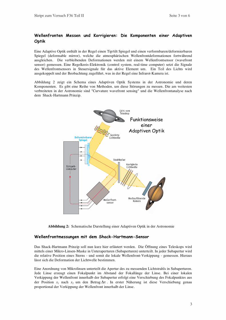
Wellenfronten Messen und Korrigieren: Die Komponenten einer Adaptiven Optik Eine Adaptive Optik enthält in der Regel einen Tip/tilt Spiegel und einen verformbaren/deformierbaren Spiegel (deformable mirror), welche die atmosphärischen Wellenfrontdeformationen fortwährend ausgleichen. Die verbleibenden Deformationen werden mit einem Wellenfrontsensor (wavefront sensor) gemessen. Eine Regelkreis-Elektronik (control system, real-time computer) setzt die Signale des Wellenfrontsensors in Steuersignale für das aktive Element um. Ein Teil des Lichts wird ausgekoppelt und der Beobachtung zugeführt, was in der Regel eine Infrarot-Kamera ist. Abbildung 2 zeigt ein Schema eines Adaptiven Optik Systems in der Astronomie und deren Komponenten. Es gibt eine Reihe von Methoden, um diese Störungen zu messen. Die am weitesten verbreiteten in der Astronomie sind "Curvature wavefront sensing" und die Wellenfrontanalyse nach dem Shack-Hartmann Prinzip.
Abbildung 2: Schematische Darstellung einer Adaptiven Optik in der Astronomie
Wellenfrontmessungen mit dem Shack-Hartmann-Sensor Das Shack-Hartmann Prinzip soll nun kurz hier erläutert werden. Die Öffnung eines Teleskops wird mittels einer Mikro-Linsen-Maske in Unteraperturen (Subaperturen) unterteilt. In jeder Subapertur wird die relative Position eines Sterns - und somit die lokale Wellenfront-Verkippung - gemessen. Hieraus lässt sich die Deformation der Lichtwelle bestimmen. Eine Anordnung von Mikrolinsen unterteilt die Apertur des zu messenden Lichtstrahls in Subaperturen. Jede Linse erzeugt einen Fokalpunkt im Abstand der Fokallänge der Linse. Bei einer lokalen Verkippung der Wellenfront innerhalb der Subapertur erfolgt eine Verschiebung des Fokalpunktes aus der Position x1 nach x2 um den Betrag x! . In erster Näherung ist diese Verschiebung genau proportional der Verkippung der Wellenfront innerhalb der Linse.
Skript zum Versuch F36 Teil II Seite 4 von 6
4
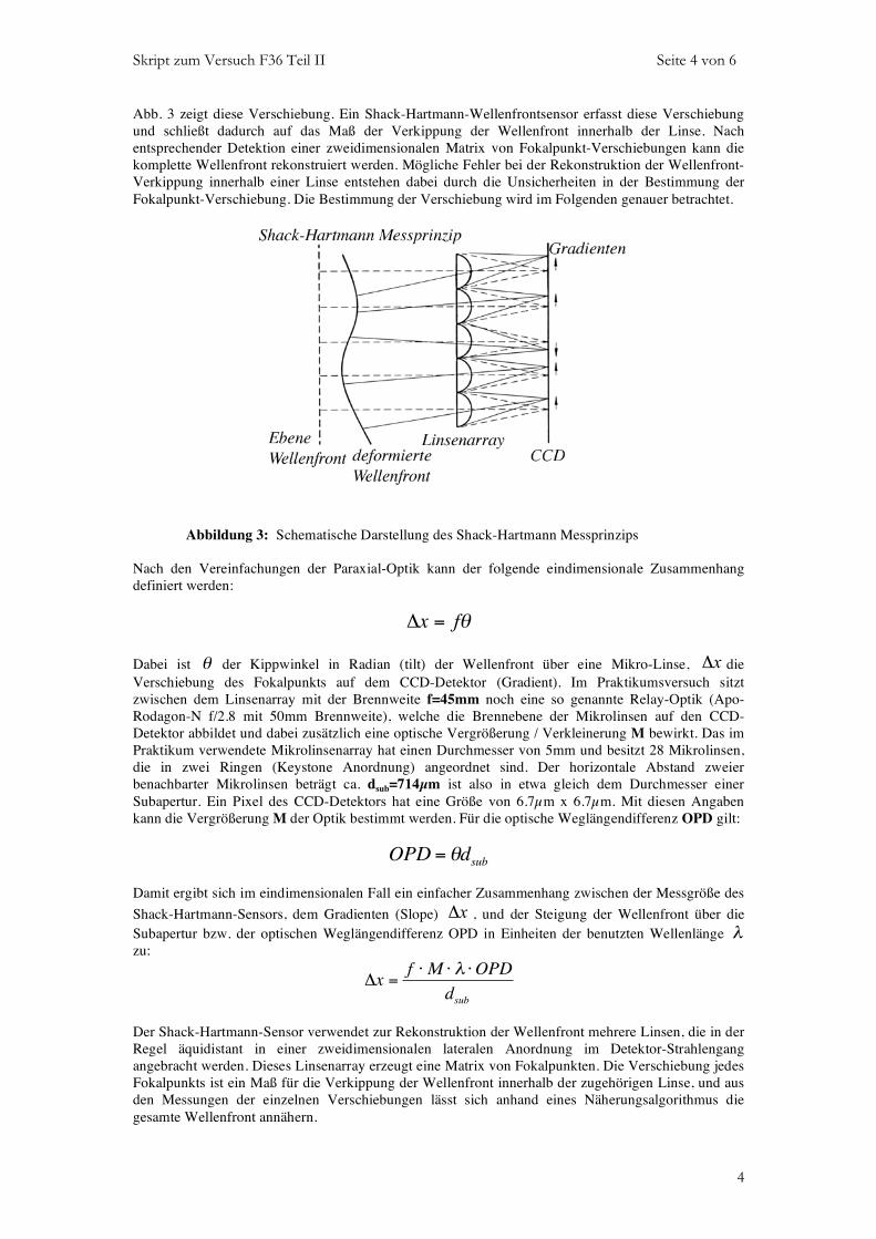
Abb. 3 zeigt diese Verschiebung. Ein Shack-Hartmann-Wellenfrontsensor erfasst diese Verschiebung und schließt dadurch auf das Maß der Verkippung der Wellenfront innerhalb der Linse. Nach entsprechender Detektion einer zweidimensionalen Matrix von Fokalpunkt-Verschiebungen kann die komplette Wellenfront rekonstruiert werden. Mögliche Fehler bei der Rekonstruktion der Wellenfront-Verkippung innerhalb einer Linse entstehen dabei durch die Unsicherheiten in der Bestimmung der Fokalpunkt-Verschiebung. Die Bestimmung der Verschiebung wird im Folgenden genauer betrachtet.
Abbildung 3: Schematische Darstellung des Shack-Hartmann Messprinzips Nach den Vereinfachungen der Paraxial-Optik kann der folgende eindimensionale Zusammenhang definiert werden:
!
"x = f# Dabei ist
!
" der Kippwinkel in Radian (tilt) der Wellenfront über eine Mikro-Linse, x! die Verschiebung des Fokalpunkts auf dem CCD-Detektor (Gradient). Im Praktikumsversuch sitzt zwischen dem Linsenarray mit der Brennweite f=45mm noch eine so genannte Relay-Optik (Apo-Rodagon-N f/2.8 mit 50mm Brennweite), welche die Brennebene der Mikrolinsen auf den CCD-Detektor abbildet und dabei zusätzlich eine optische Vergrößerung / Verkleinerung M bewirkt. Das im Praktikum verwendete Mikrolinsenarray hat einen Durchmesser von 5mm und besitzt 28 Mikrolinsen, die in zwei Ringen (Keystone Anordnung) angeordnet sind. Der horizontale Abstand zweier benachbarter Mikrolinsen beträgt ca. dsub=714µm ist also in etwa gleich dem Durchmesser einer Subapertur. Ein Pixel des CCD-Detektors hat eine Größe von 6.7µm x 6.7µm. Mit diesen Angaben kann die Vergrößerung M der Optik bestimmt werden. Für die optische Weglängendifferenz OPD gilt:
!
OPD = "dsub
Damit ergibt sich im eindimensionalen Fall ein einfacher Zusammenhang zwischen der Messgröße des Shack-Hartmann-Sensors, dem Gradienten (Slope) x! , und der Steigung der Wellenfront über die Subapertur bzw. der optischen Weglängendifferenz OPD in Einheiten der benutzten Wellenlänge
!
" zu:
!
"x =f # M # $ #OPD
dsub
Der Shack-Hartmann-Sensor verwendet zur Rekonstruktion der Wellenfront mehrere Linsen, die in der Regel äquidistant in einer zweidimensionalen lateralen Anordnung im Detektor-Strahlengang angebracht werden. Dieses Linsenarray erzeugt eine Matrix von Fokalpunkten. Die Verschiebung jedes Fokalpunkts ist ein Maß für die Verkippung der Wellenfront innerhalb der zugehörigen Linse, und aus den Messungen der einzelnen Verschiebungen lässt sich anhand eines Näherungsalgorithmus die gesamte Wellenfront annähern.

Skript zum Versuch F36 Teil II Seite 5 von 6
5
Zur Detektion der Abbildungen eines Shack-Hartmann Linsenarrays setzt man meist eine CCD ein. Für die Detektion der Aufnahme jeder einzelnen Subapertur benötigt man einen quadratischen Ausschnitt von mindestens 2 x 2 Pixeln. Um optische Übersprechen (engl. Crosstalk) zwischen den Subaperturen zu vermeiden, wird zwischen die Subaperturen ein Sicherheitsabstand von mindestens ein Pixel Breite eingebracht. Nach diesem Prinzip arbeiten manche Shack-Hartmann-Systeme mit 3 x 3 Pixeln pro Subapertur. Eine gängige Alternative sind 4 x 4 bis 8 x 8 Pixel pro Subapertur (z.B. Starfire Optical Range, Adaptive Optik des Calar Alto ALFA Systems). Je größer die Pixelzahl, desto dynamischer ist der Wellenfrontsensor (d.h. stärkere Verkippungen können gemessen werden) und die Objekte dürfen eine größere Ausdehnung besitzen. Jedoch ist dies mit stärkerem Rauschen verbunden, weil die Anzahl der auszulesenden Pixel und die Auslesezeit zunehmen. Zur Steigerung der Auslesegeschwindigkeit und Verringerung des Ausleserauschens können die 8 x 8 Pixel zu so genannten Superpixel "gebinnt" werden, wodurch man eine geringere Zahl von (größeren) Pixeln simuliert. Von Shack-Hartmann-Gradienten zu Wellenfronten Wie aus der vorhergegangenen Beschreibung hervorgeht, kann man für jede Subapertur I, die mittleren Weglängendifferenzen bestimmen durch
!
dsub"xi
fM#=OPDxi
und
!
dsub"yi
fM#=OPDyi
,
und aus diesen Informationen die Wellenfront über die gesamte Mikrolinsenmaske rekonstruieren. Im allgemeinen kann eine Wellenfront als eine Summe Polynome höherer Ordnung mit jeweiligen Koeffizienten repräsentiert werden. Eine in der Optik häufig verwendete Darstellung wurde von F. Zernike 1934 zur Beschreibung der Qualität von Hohlspiegeln entwickelt. Die Zernike-Polynome besitzen Orthogonalität und den typischen Formen von Aberrationen wie zum Beispiel Z4=Defokus, Z5=Astigmatismus, Z7 =Koma und sphärische Aberrationen lassen sich dedizierte Koeffizienten zuordnen (siehe Tabelle 1.1). Zernike beschreibt eine Wellenfront W(x,y) als Summe aus den Produkten dieser Polynome Zn(x,y) mit den Koeffizienten Cn
),(),(0
yxZCyxW nn!"
= .
Mit:
Tabelle 1: Einige Zernike Polynome in kartesischen Koordinaten.

Skript zum Versuch F36 Teil II Seite 6 von 6
6
Versuchsdurchführung und Messungen Im Rahmen des F-Praktikums sollen folgende Aufbauten und Messungen durchgeführt werden:
1. Aufbau eines Shack-Hartmann-Sensors aus den zur Verfügung gestellten Einzelkomponenten auf einer optischen Bank.
2. Aufnahmen von Shack-Hartmann Bildern (Shack-Hartmann Spot Images) mit einer Laserlichtquelle.
3. Auffinden des besten Fokus als Funktion der Position der Relay-Optik auf der optischen Bank.
4. Messung von Shack-Hartmann Gradienten für verschiedene optische Aberrationen. 5. Bestimmung einer Wellenfront aus den Messdaten (Shack-Hartmann Gradientenbild). Für die lange Auswertung zusätzlich: 6. Rekonstruktion von Wellenfronten mit Hilfe der Zernike Polynome (Modenrekonstruktion,
modal reconstruction). 7. Alternativ zu Punkt 6: Lokale Rekonstruktion der Wellenfronten mit Hilfe eines geeigneten
2D Oberflächenfits.
Beispiel einer Shack-Hartmann-Aufnahme.
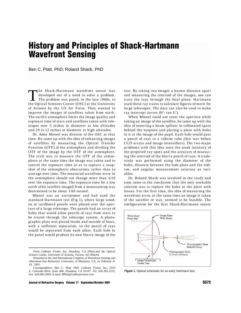
The Shack-Hartmann wavefront sensor wasdeveloped out of a need to solve a problem.The problem was posed, in the late 1960s, to
the Optical Sciences Center (OSC) at the Universityof Arizona by the US Air Force. They wanted toimprove the images of satellites taken from earth.The earth’s atmosphere limits the image quality andexposure time of stars and satellites taken with tele-scopes over 5 inches in diameter at low altitudesand 10 to 12 inches in diameter at high altitudes.
Dr. Aden Mienel was director of the OSC at thattime. He came up with the idea of enhancing imagesof satellites by measuring the Optical TransferFunction (OTF) of the atmosphere and dividing theOTF of the image by the OTF of the atmosphere.The trick was to measure the OTF of the atmos-phere at the same time the image was taken and tocontrol the exposure time so as to capture a snap-shot of the atmospheric aberrations rather than toaverage over time. The measured wavefront error inthe atmosphere should not change more than �/10over the exposure time. The exposure time for a lowearth orbit satellite imaged from a mountaintop wasdetermined to be about 1/60 second.
Mienel was an astronomer and had used thestandard Hartmann test (Fig 1), where large wood-en or cardboard panels were placed over the aper-ture of a large telescope. The panels had an array ofholes that would allow pencils of rays from stars tobe traced through the telescope system. A photo-graphic plate was placed inside and outside of focus,with a sufficient separation, so the pencil of rayswould be separated from each other. Each hole inthe panel would produce its own blurry image of the
star. By taking two images a known distance apartand measuring the centroid of the images, one cantrace the rays through the focal plane. Hartmannused these ray traces to calculate figures of merit forlarge telescopes. The data can also be used to makeray intercept curves (H'- tan U').
When Mienel could not cover the aperture whiletaking an image of the satellite, he came up with theidea of inserting a beam splitter in collimated spacebehind the eyepiece and placing a plate with holesin it at the image of the pupil. Each hole would passa pencil of rays to a vidicon tube (this was beforeCCD arrays and image intensifiers). The two majorproblems with this idea were the weak intensity ofthe projected ray spots and the accuracy of measur-ing the centroid of the blurry pencil of rays. A trade-study was performed using the diameter of theholes, distance between the hole plate and the vidi-con, and angular measurement accuracy as vari-ables.
Dr. Roland Shack was involved in the study andsoon came to the conclusion that the only workablesolution was to replace the holes in the plate withlenses. For the first time, the idea of measuring thewavefront error, at the same time an image is takenof the satellite or star, seemed to be feasible. Theconfiguration for the first Shack-Hartmann sensor
History and Principles of Shack-HartmannWavefront SensingBen C. Platt, PhD; Roland Shack, PhD
From Calhoun Vision, Inc, Pasadena, CA (Platt) and the OpticalScience Center, University of Arizona, Tucson, AZ (Shack).
Presented at the 2nd International Congress of Wavefront Sensing andAberration-free Refractive Correction, in Monterey, CA, on February 9-10, 2001.
Correspondence: Ben C. Platt, PhD, Calhoun Vision, Inc, 2555E. Colorado Blvd, Suite 400, Pasadena, CA 91107. Tel: 626.395.5215;Fax: 626.685.2003; E-mail: [email protected]
Journal of Refractive Surgery Volume 17 September/October 2001 S573
Figure 1. Optical schematic for an early Hartmann test.
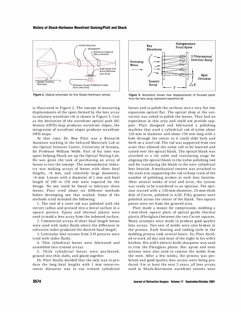
is illustrated in Figure 2. The concept of measuringdisplacements of the spots formed by the lens arrayto calculate wavefront tilt is shown in Figure 3. Justas the derivative of the wavefront optical path dif-ference (OPD) map produces wavefront slopes, theintegration of wavefront slopes produces wavefrontOPD maps.
At that time, Dr. Ben Platt was a ResearchAssociate working in the Infrared Materials Lab atthe Optical Sciences Center, University of Arizona,for Professor William Wolfe. Part of his time wasspent helping Shack set up the Optical Testing Lab.He was given the task of purchasing an array oflenses to test the concept. The semiconductor indus-try was making arrays of lenses with short focallengths, ~6 mm, and relatively large diameters,~6 mm. Lenses with a diameter of 1 mm and focallength of 100 to 150 mm were required for thedesign. No one could be found to fabricate theselenses. Platt tried about six different methodsbefore developing one that worked. Some of themethods tried included the following:
1. The end of a steel rod was polished with thecorrect radius and pressed into a metal surface in asquare pattern. Epoxy and thermal plastic wereused to mold a lens array from the indented surface.
2. Commercial arrays of short focal length lenseswere used with index fluids where the difference inrefractive index produced the desired focal length.
3. Lenticular lens screens from 3-D pictures weretried with index fluids.
4. Thin cylindrical lenses were fabricated andassembled into crossed arrays.
5. Thick cylindrical lenses were purchased,ground into thin slabs, and glued together.
Dr. Platt finally decided that the only way to pro-duce the long focal lengths with 1 mm center-to-center distances was to use crossed cylindrical
lenses and to polish the surfaces into a very flat lowexpansion optical flat. The optical shop at the uni-versity was asked to polish the lenses. They had noexperience in this area and could not provide sup-port. Platt designed and fabricated a polishingmachine that used a cylindrical rod of nylon about120 mm in diameter and about 150 mm long with ahole through the center so it could slide back andforth on a steel rod. The rod was supported from twoarms that allowed the nylon roll to be lowered andraised over the optical blank. The optical blank wasattached to a tilt table and translating stage foraligning the optical blank to the nylon polishing tooland for translating the blank to the next cylindricallens location. A mechanical counter was attached tothe steel arm supporting the rod to keep track of thenumber of polishing strokes at each lens location.After several weeks of trial and error, the systemwas ready to be transfered to an optician. The opti-cian started with a 150-mm-diameter, 25-mm-thickdisk of Cervet, polished to �/20. Fifty grooves werepolished across the center of the blank. Two squarepieces were cut from the grooved area.
Platt made a mount for compression, molding a1-mm-thick square plate of optical grade thermalplastic (Plexiglass) between the two Cervet squares.Many attempts were made to produce good qualitylens arrays. Two sets of molds were also broken inthe process. Each heating and cooling cycle in themolding process took several hours. So, Platt decid-ed to work all day and most of the night in his wife’skitchen. His wife’s electric knife sharpener was usedto trim the Plexiglass plates. Her apron and ovenmittens were also used to remove the molds fromthe oven. After a few weeks, the process was per-fected and good quality lens arrays were being pro-duced. For at least the next 5 years, all lens arraysused in Shack-Hartmann wavefront sensors were
S574 Journal of Refractive Surgery Volume 17 September/October 2001
History of Shack-Hartmann Wavefront Sensing/Platt and Shack
Figure 2. Optical schematic for first Shack-Hartmann sensor. Figure 3. Illustration shows how displacements of focused spotsfrom the lens array represent wavefront tilt.
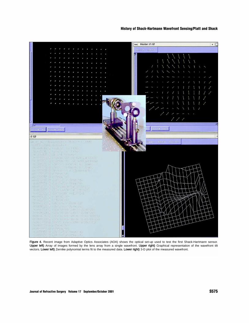
Journal of Refractive Surgery Volume 17 September/October 2001 S575
History of Shack-Hartmann Wavefront Sensing/Platt and Shack
Figure 4. Recent image from Adaptive Optics Associates (AOA) shows the optical set-up used to test the first Shack-Hartmann sensor.Upper left) Array of images formed by the lens array from a single wavefront. Upper right) Graphical representation of the wavefront tiltvectors. Lower left) Zernike polynomial terms fit to the measured data. Lower right) 3-D plot of the measured wavefront.
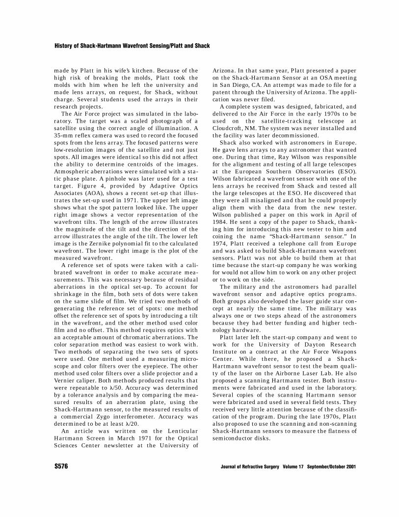
made by Platt in his wife’s kitchen. Because of thehigh risk of breaking the molds, Platt took themolds with him when he left the university andmade lens arrays, on request, for Shack, withoutcharge. Several students used the arrays in theirresearch projects.
The Air Force project was simulated in the labo-ratory. The target was a scaled photograph of asatellite using the correct angle of illumination. A35-mm reflex camera was used to record the focusedspots from the lens array. The focused patterns werelow-resolution images of the satellite and not justspots. All images were identical so this did not affectthe ability to determine centroids of the images.Atmospheric aberrations were simulated with a sta-tic phase plate. A pinhole was later used for a testtarget. Figure 4, provided by Adaptive OpticsAssociates (AOA), shows a recent set-up that illus-trates the set-up used in 1971. The upper left imageshows what the spot pattern looked like. The upperright image shows a vector representation of thewavefront tilts. The length of the arrow illustratesthe magnitude of the tilt and the direction of thearrow illustrates the angle of the tilt. The lower leftimage is the Zernike polynomial fit to the calculatedwavefront. The lower right image is the plot of themeasured wavefront.
A reference set of spots were taken with a cali-brated wavefront in order to make accurate mea-surements. This was necessary because of residualaberrations in the optical set-up. To account forshrinkage in the film, both sets of dots were takenon the same slide of film. We tried two methods ofgenerating the reference set of spots: one methodoffset the reference set of spots by introducing a tiltin the wavefront, and the other method used colorfilm and no offset. This method requires optics withan acceptable amount of chromatic aberrations. Thecolor separation method was easiest to work with.Two methods of separating the two sets of spotswere used. One method used a measuring micro-scope and color filters over the eyepiece. The othermethod used color filters over a slide projector and aVernier caliper. Both methods produced results thatwere repeatable to �/50. Accuracy was determinedby a tolerance analysis and by comparing the mea-sured results of an aberration plate, using theShack-Hartmann sensor, to the measured results ofa commercial Zygo interferometer. Accuracy wasdetermined to be at least �/20.
An article was written on the LenticularHartmann Screen in March 1971 for the OpticalSciences Center newsletter at the University of
Arizona. In that same year, Platt presented a paperon the Shack-Hartmann Sensor at an OSA meetingin San Diego, CA. An attempt was made to file for apatent through the University of Arizona. The appli-cation was never filed.
A complete system was designed, fabricated, anddelivered to the Air Force in the early 1970s to beused on the satellite-tracking telescope atCloudcroft, NM. The system was never installed andthe facility was later decommissioned.
Shack also worked with astronomers in Europe.He gave lens arrays to any astronomer that wantedone. During that time, Ray Wilson was responsiblefor the alignment and testing of all large telescopesat the European Southern Observatories (ESO).Wilson fabricated a wavefront sensor with one of thelens arrays he received from Shack and tested allthe large telescopes at the ESO. He discovered thatthey were all misaligned and that he could properlyalign them with the data from the new tester.Wilson published a paper on this work in April of1984. He sent a copy of the paper to Shack, thank-ing him for introducing this new tester to him andcoining the name “Shack-Hartmann sensor.” In1974, Platt received a telephone call from Europeand was asked to build Shack-Hartmann wavefrontsensors. Platt was not able to build them at thattime because the start-up company he was workingfor would not allow him to work on any other projector to work on the side.
The military and the astronomers had parallelwavefront sensor and adaptive optics programs.Both groups also developed the laser guide star con-cept at nearly the same time. The military wasalways one or two steps ahead of the astronomersbecause they had better funding and higher tech-nology hardware.
Platt later left the start-up company and went towork for the University of Dayton ResearchInstitute on a contract at the Air Force WeaponsCenter. While there, he proposed a Shack-Hartmann wavefront sensor to test the beam quali-ty of the laser on the Airborne Laser Lab. He alsoproposed a scanning Hartmann tester. Both instru-ments were fabricated and used in the laboratory.Several copies of the scanning Hartmann sensorwere fabricated and used in several field tests. Theyreceived very little attention because of the classifi-cation of the program. During the late 1970s, Plattalso proposed to use the scanning and non-scanningShack-Hartmann sensors to measure the flatness ofsemiconductor disks.
S576 Journal of Refractive Surgery Volume 17 September/October 2001
History of Shack-Hartmann Wavefront Sensing/Platt and Shack
During the same time period, Adaptive OpticsAssociates (AOA) was developing (for the Air Force)adaptive optics that would compensate for theearth’s atmosphere. They started out with a scan-ning Hartmann system and ended up with a stan-dard Shack-Hartmann wavefront sensor using lensarrays. AOA developed their own lens arrays andeventually sold them commercially. MassachusettsInstitute of Technology (MIT) developed methods formaking lens arrays using binary optics. Soon after-ward, other organizations started making lensarrays using binary optics. When the lens arraysbecame easily available, more and more peoplestarted experimenting with the Shack-Hartmannsensor. Now, several companies are selling Shack-Hartmann sensors commercially.
Software to convert the 2-D tilt data into 2-Dwavefront data is another major part of the wave-front sensor. The first software program was writtenat the University of Arizona. They had developed aprogram for reducing interferograms. This programwas later modified to reduce shearing interfero-grams. Since shearing interferograms representwavefront tilt, it was easy to modify this program toreduce Shack-Hartmann data. This program wasmade available to the public for the cost of copying.AOA developed its own software package for com-mercial and military applications. Most of the astro-nomical groups also developed their own software.Soon, the software was easily available.
In the mid 1980s, Dr. Josef Bille, from theUniversity of Erlangen-Nurnberg, started workingwith Shack to use the lens array for measuring theprofile of the cornea. Bille was the first to use thesensor in ophthalmology. He used it first to measurethe profile of the cornea and later to measure aber-rations in the eye, by projecting a point source ontothe retina. His first published paper was in 1989.
In 1985, Platt formed a company to provide opti-cal instruments and consulting support to the
government and commercial organizations. One ofthe instruments he wanted to produce commerciallywas the Shack-Hartmann sensor. He wrote severalproposals for different applications, including anapplication to the National Eye Institute (NEI) ofthe National Institutes of Health (NIH) for cornealtopography. By the time the proposal was resubmit-ted, photorefractive keratectomy (PRK) was replac-ing radial keratotomy, and NEI was looking only atcorneal topography instruments that could measurethe profile of a diffuse surface.
The next major milestone in the United States forusing the Shack-Hartmann sensor in ophthalmolo-gy occurred with the work of David Williams at theUniversity of Rochester. He was the first (in theUnited States) to use the Shack-Hartmann sensorfor measuring aberrations in the eye. He alsodemonstrated improved imaging of the retina bycoupling the Shack-Hartmann wavefront sensor to adeformable mirror, generating the first adaptiveoptics system used in ophthalmology.
The United States military started using theShack-Hartmann sensor in 1974 to test lasers, andin the early 1980s, in adaptive optical systems.From 1974 to 1996, Platt wrote proposals to use theShack-Hartmann sensor for applications rangingfrom aligning telescopes, testing lasers, testingsemiconductor disks, to measuring the profile of thecornea. Current applications for the Shack-Hartmann sensor in ophthalmology, astronomy,adaptive optics, optical alignment, and commercialoptical testing are too numerous to list. Hundreds ofprograms using the Shack-Hartmann sensor can befound on the Internet. It is currently the most pop-ular wavefront sensor in the world for applicationsother than standard optical testing of optical com-ponents. Although the Shack-Hartmann sensor isbeing used to test optical components, it is notexpected to replace the interferometer—only tocomplement it.
Journal of Refractive Surgery Volume 17 September/October 2001 S577
History of Shack-Hartmann Wavefront Sensing/Platt and Shack
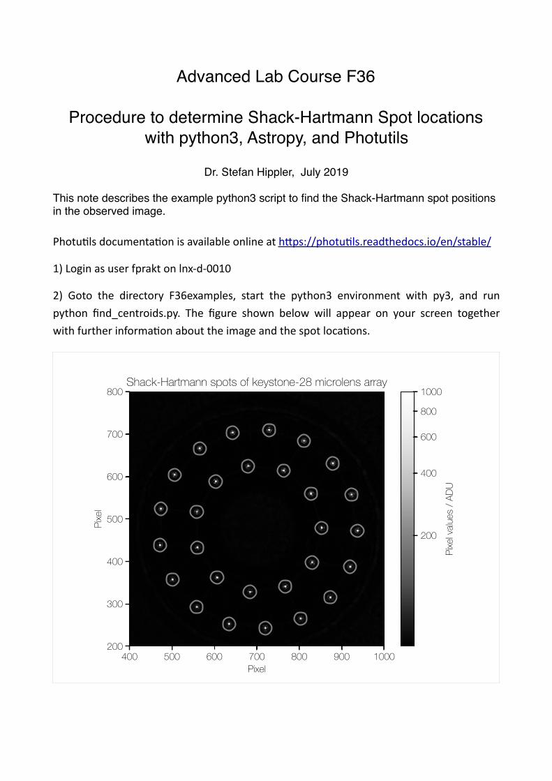
Advanced Lab Course F36
Procedure to determine Shack-Hartmann Spot locationswith python3, Astropy, and Photutils
Dr. Stefan Hippler, July 2019
This note describes the example python3 script to find the Shack-Hartmann spot positions in the observed image.Photu&lsdocumenta&onisavailableonlineath3ps://photu&ls.readthedocs.io/en/stable/
1)Loginasuserfpraktonlnx-d-0010
2) Goto the directory F36examples, start the python3 environment with py3, and runpython find_centroids.py. The figure shown below will appear on your screen togetherwithfurtherinforma&onabouttheimageandthespotloca&ons.
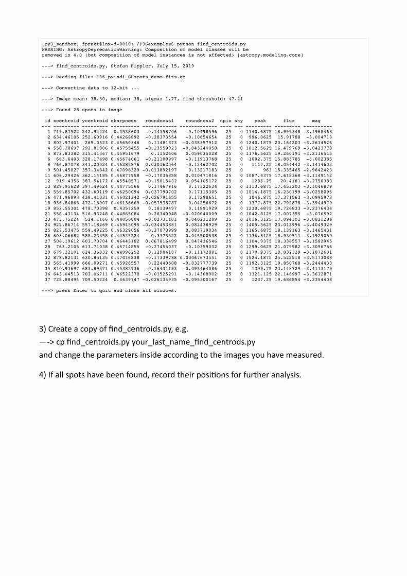
3)Createacopyoffind_centroids.py,e.g. —->cpfind_centroids.pyyour_last_name_find_centrods.pyandchangetheparametersinsideaccordingtotheimagesyouhavemeasured.
4)Ifallspotshavebeenfound,recordtheirposi&onsforfurtheranalysis.
(py3_sandbox) fprakt@lnx-d-0010:~/F36examples$ python find_centroids.py WARNING: AstropyDeprecationWarning: Composition of model classes will beremoved in 4.0 (but composition of model instances is not affected) [astropy.modeling.core]
---> find_centroids.py, Stefan Hippler, July 15, 2019
---> Reading file: F36_pyindi_SHspots_demo.fits.gz
---> Converting data to 12-bit ...
---> Image mean: 38.50, median: 38, sigma: 1.77, find threshold: 47.21
---> Found 28 spots in image
id xcentroid ycentroid sharpness roundness1 roundness2 npix sky peak flux mag--- --------- --------- ---------- ------------ ------------- ---- --- --------- --------- ---------- 1 719.87522 242.94224 0.4538603 -0.14358706 -0.10498596 25 0 1140.6875 18.999348 -3.1968468 2 634.46105 252.60916 0.44268892 -0.28373554 -0.10654654 25 0 996.0625 15.91788 -3.004713 3 802.97401 265.0523 0.45650346 0.11481873 -0.038357912 25 0 1240.1875 20.164203 -3.2614526 4 558.28697 292.81806 0.45755455 -0.23559923 -0.043240058 25 0 1012.5625 16.479769 -3.0423778 5 872.83382 315.41367 0.45951679 0.1152606 0.059035028 25 0 1176.5625 19.260191 -3.2116515 6 683.6403 328.17498 0.45674061 -0.21109997 -0.11913768 25 0 1002.375 15.883785 -3.002385 8 766.87078 341.20024 0.46285876 0.030162564 -0.12462702 25 0 1117.25 18.054442 -3.1414602 9 501.45027 357.34842 0.47098329 -0.013892197 0.13217183 25 0 963 15.335465 -2.9642423 11 606.29426 362.14185 0.46877958 -0.17035858 0.010471816 25 0 1087.4375 17.618368 -3.1149142 12 919.4356 387.54172 0.45540571 -0.15015432 0.054105172 25 0 1286.25 20.4181 -3.2750383 13 829.95628 397.49624 0.44775566 0.17467916 0.17322634 25 0 1113.6875 17.453203 -3.1046879 15 559.85702 432.60119 0.46250094 0.037790702 0.17115305 25 0 1014.1875 16.230199 -3.0258096 16 471.96893 438.41031 0.46021342 -0.026791655 0.17298651 25 0 1046.875 17.371563 -3.0995973 18 936.84865 472.15907 0.46136669 -0.057538787 0.04256672 25 0 1377.875 22.792878 -3.3944979 19 852.55301 478.70398 0.4357259 0.18139497 0.11891929 25 0 1230.6875 19.726833 -3.2376434 21 558.43134 516.93248 0.44865084 0.26340048 -0.020040009 25 0 1042.8125 17.007355 -3.076592 23 473.75224 524.1166 0.44050804 -0.02731101 0.040231289 25 0 1016.3125 17.094301 -3.0821284 24 922.86714 557.18269 0.46945095 -0.034453881 0.082438929 25 0 1405.5625 23.012996 -3.4049329 25 827.53475 559.49225 0.46329056 -0.37070999 0.083719034 25 0 1165.6875 18.139163 -3.1465431 26 603.06682 588.23358 0.44535224 0.3375322 0.045500538 25 0 1136.8125 18.930511 -3.1929059 27 506.19612 603.70704 0.46443182 0.067816499 0.047436546 25 0 1104.9375 18.336557 -3.1582945 28 763.2105 613.71038 0.45714855 -0.27455037 -0.10359032 25 0 1299.0625 21.079982 -3.3096756 29 679.22101 624.35032 0.44996252 0.12984187 -0.11172801 25 0 1170.9375 18.832329 -3.1872601 32 878.82131 630.85135 0.47016838 -0.17339788 0.00067673551 25 0 1524.1875 25.522518 -3.5173088 33 565.41999 666.09271 0.45926557 0.22440608 -0.032777739 25 0 1192.3125 19.850768 -3.2444433 35 810.93697 683.89371 0.45382936 -0.16431193 -0.095464086 25 0 1399.75 23.148729 -3.4113179 36 643.04513 703.06711 0.46522378 -0.01525291 -0.14308902 25 0 1321.125 22.146997 -3.3632871 37 728.88494 709.50224 0.4639747 -0.026134935 -0.095300167 25 0 1237.25 19.686854 -3.2354408
---> press Enter to quit and close all windows.
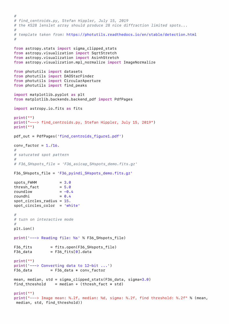
## find_centroids.py, Stefan Hippler, July 15, 2019# the KS28 lenslet array should produce 28 nice diffraction limited spots...## template taken from: https://photutils.readthedocs.io/en/stable/detection.html#
from astropy.stats import sigma_clipped_statsfrom astropy.visualization import SqrtStretchfrom astropy.visualization import AsinhStretchfrom astropy.visualization.mpl_normalize import ImageNormalize
from photutils import datasetsfrom photutils import DAOStarFinderfrom photutils import CircularAperturefrom photutils import find_peaks
import matplotlib.pyplot as pltfrom matplotlib.backends.backend_pdf import PdfPages
import astropy.io.fits as fits
print("")print("---> find_centroids.py, Stefan Hippler, July 15, 2019")print("")
pdf_out = PdfPages('find_centroids_figure1.pdf')
conv_factor = 1./16.## saturated spot pattern## F36_SHspots_file = 'F36_asicap_SHspots_demo.fits.gz'
F36_SHspots_file = 'F36_pyindi_SHspots_demo.fits.gz'
spots_FWHM = 3.0thresh_fact = 5.0roundlow = -0.4roundhi = 0.4spot_circles_radius = 15.spot_circles_color = 'white'
## turn on interactive mode#plt.ion()
print('---> Reading file: %s' % F36_SHspots_file)
F36_fits = fits.open(F36_SHspots_file)F36_data = F36_fits[0].data
print("")print('---> Converting data to 12-bit ...') F36_data = F36_data * conv_factor
mean, median, std = sigma_clipped_stats(F36_data, sigma=3.0) find_threshold = median + (thresh_fact * std)
print("")print("---> Image mean: %.2f, median: %d, sigma: %.2f, find threshold: %.2f" % (mean, median, std, find_threshold))
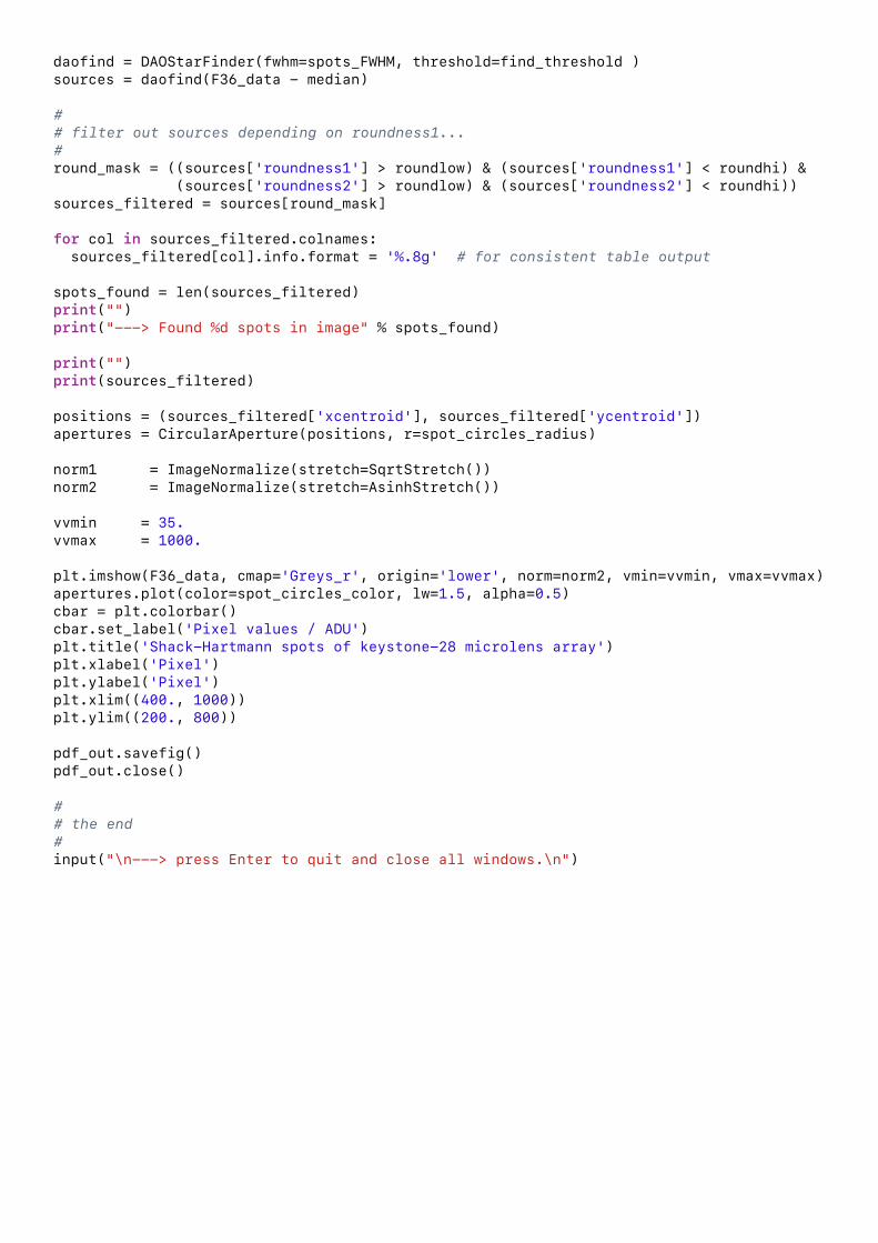
daofind = DAOStarFinder(fwhm=spots_FWHM, threshold=find_threshold ) sources = daofind(F36_data - median)
## filter out sources depending on roundness1...#round_mask = ((sources['roundness1'] > roundlow) & (sources['roundness1'] < roundhi) & (sources['roundness2'] > roundlow) & (sources['roundness2'] < roundhi))sources_filtered = sources[round_mask]
for col in sources_filtered.colnames: sources_filtered[col].info.format = '%.8g' # for consistent table output
spots_found = len(sources_filtered)print("")print("---> Found %d spots in image" % spots_found)
print("")print(sources_filtered)
positions = (sources_filtered['xcentroid'], sources_filtered['ycentroid'])apertures = CircularAperture(positions, r=spot_circles_radius)
norm1 = ImageNormalize(stretch=SqrtStretch())norm2 = ImageNormalize(stretch=AsinhStretch())
vvmin = 35.vvmax = 1000.
plt.imshow(F36_data, cmap='Greys_r', origin='lower', norm=norm2, vmin=vvmin, vmax=vvmax)apertures.plot(color=spot_circles_color, lw=1.5, alpha=0.5)cbar = plt.colorbar()cbar.set_label('Pixel values / ADU')plt.title('Shack-Hartmann spots of keystone-28 microlens array')plt.xlabel('Pixel')plt.ylabel('Pixel')plt.xlim((400., 1000))plt.ylim((200., 800))
pdf_out.savefig()pdf_out.close()
## the end#input("\n---> press Enter to quit and close all windows.\n")
Zernike Polynomials1 Introduction
Often, to aid in the interpretation of optical test results it is convenient to express wavefront data in polynomial form. Zernike polynomials are often used for thispurpose since they are made up of terms that are of the same form as the types of aberrations often observed in optical tests (Zernike, 1934). This is not to say thatZernike polynomials are the best polynomials for fitting test data. Sometimes Zernike polynomials give a poor representation of the wavefront data. For example,Zernikes have little value when air turbulence is present. Likewise, fabrication errors in the single point diamond turning process cannot be represented using areasonable number of terms in the Zernike polynomial. In the testing of conical optical elements, additional terms must be added to Zernike polynomials to accuratelyrepresent alignment errors. The blind use of Zernike polynomials to represent test results can lead to disastrous results.
Zernike polynomials are one of an infinite number of complete sets of polynomials in two variables, r and q, that are orthogonal in a continuous fashion over the interiorof a unit circle. It is important to note that the Zernikes are orthogonal only in a continuous fashion over the interior of a unit circle, and in general they will not beorthogonal over a discrete set of data points within a unit circle.
Zernike polynomials have three properties that distinguish them from other sets of orthogonal polynomials. First, they have simple rotational symmetry properties thatlead to a polynomial product of the form
r@ρD g@θD,where g[q] is a continuous function that repeats self every 2p radians and satisfies the requirement that rotating the coordinate system by an angle a does not change theform of the polynomial. That is
g@θ + αD = g@θD g@αD.The set of trigonometric functions
g@θD = ± m θ,where m is any positive integer or zero, meets these requirements.The second property of Zernike polynomials is that the radial function must be a polynomial in r of degree 2n and contain no power of r less than m. The third propertyis that r[r] must be even if m is even, and odd if m is odd.
The radial polynomials can be derived as a special case of Jacobi polynomials, and tabulated as r@n, m, rD. Their orthogonality and normalization properties are givenby
‡0
1
r@n, m, ρD r@n', m, ρD ρ ρ =1
2 Hn + 1L KroneckerDelta@n − n'Dand
ZernikePolynomialsForTheWeb.nb James C. Wyant, 2003 1
r@n, m, 1D = 1.As stated above, r[n, m, r] is a polynomial of order 2n and it can be written as
r@n_, m_, ρ_D := ‚s=0
n−m
H−1Ls H2 n − m − sL!
s! Hn − sL! Hn − m − sL! ρ2 Hn−sL−m
In practice, the radial polynomials are combined with sines and cosines rather than with a complex exponential. It is convenient to write
rcos@n_, m_, ρ_D := r@n, m, ρD Cos@m θDand
rsin@n_, m_, ρ_D := r@n, m, ρD Sin@m θDThe final Zernike polynomial series for the wavefront opd Dw can be written as
∆w@ρ_, θ_D := ∆w¯¯
+ „n=1
nmax ikjjjjja@nD r@n, 0, ρD + ‚
m=1
n
Hb@n, mD rcos@n, m, ρD + c@n, mD rsin@n, m, ρDLy{zzzzz
where Dw[r, q] is the mean wavefront opd, and a[n], b[n,m], and c[n,m] are individual polynomial coefficients. For a symmetrical optical system, the wave aberrationsare symmetrical about the tangential plane and only even functions of q are allowed. In general, however, the wavefront is not symmetric, and both sets of trigonometricterms are included.
2 Calculating Zernikes
For the example below the degree of the Zernike polynomials is selected to be 6. The value of nDegree can be changed if a different degree is desired.
The array zernikePolar contains Zernike polynomials in polar coordinates (r, q), while the array zernikeXy contains the Zernike polynomials in Cartesian, (x, y),coordinates. zernikePolarList and zernikeXyList contains the Zernike number in column 1, the n and m values in columns 2 and 3, and the Zernike polynomial incolumn 4.
nDegree = 6;
i = 0;Do@If@m == 0, 8i = i + 1, temp@iD = 8i − 1, n, m, r@n, m, ρD<<,
8i = i + 1, temp@iD = 8i − 1, n, m, Factor@rcos@n, m, ρDD<,i = i + 1, temp@iD = 8i − 1, n, m, Factor@rsin@n, m, ρDD<<D, 8n, 0, nDegree<, 8m, n, 0, −1<D;
ZernikePolynomialsForTheWeb.nb James C. Wyant, 2003 2
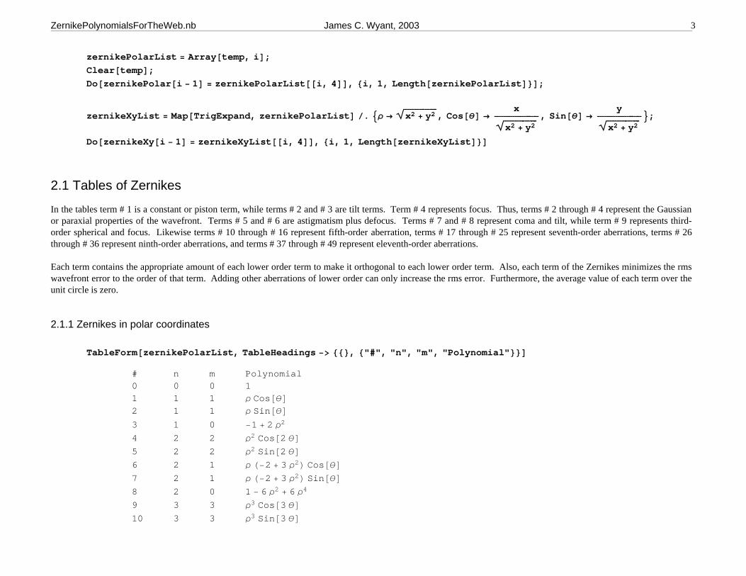
zernikePolarList = Array@temp, iD;Clear@tempD;Do@zernikePolar@i − 1D = zernikePolarList@@i, 4DD, 8i, 1, Length@zernikePolarListD<D;
zernikeXyList = Map@TrigExpand, zernikePolarListD ê. 9ρ →è!!!!!!!!!!!!!!!
x2 + y2 , Cos@θD →x
è!!!!!!!!!!!!!!!x2 + y2
, Sin@θD →y
è!!!!!!!!!!!!!!!x2 + y2
=;
Do@zernikeXy@i − 1D = zernikeXyList@@i, 4DD, 8i, 1, Length@zernikeXyListD<D
2.1 Tables of Zernikes
In the tables term # 1 is a constant or piston term, while terms # 2 and # 3 are tilt terms. Term # 4 represents focus. Thus, terms # 2 through # 4 represent the Gaussianor paraxial properties of the wavefront. Terms # 5 and # 6 are astigmatism plus defocus. Terms # 7 and # 8 represent coma and tilt, while term # 9 represents third-order spherical and focus. Likewise terms # 10 through # 16 represent fifth-order aberration, terms # 17 through # 25 represent seventh-order aberrations, terms # 26through # 36 represent ninth-order aberrations, and terms # 37 through # 49 represent eleventh-order aberrations.
Each term contains the appropriate amount of each lower order term to make it orthogonal to each lower order term. Also, each term of the Zernikes minimizes the rmswavefront error to the order of that term. Adding other aberrations of lower order can only increase the rms error. Furthermore, the average value of each term over theunit circle is zero.
2.1.1 Zernikes in polar coordinates
TableForm@zernikePolarList, TableHeadings −> 88<, 8"#", "n", "m", "Polynomial"<<D
# n m Polynomial0 0 0 11 1 1 ρ Cos@θD2 1 1 ρ Sin@θD3 1 0 −1 + 2 ρ2
4 2 2 ρ2 Cos@2 θD5 2 2 ρ2 Sin@2 θD6 2 1 ρ H−2 + 3 ρ2L Cos@θD7 2 1 ρ H−2 + 3 ρ2L Sin@θD8 2 0 1 − 6 ρ2 + 6 ρ4
9 3 3 ρ3 Cos@3 θD10 3 3 ρ3 Sin@3 θD
ZernikePolynomialsForTheWeb.nb James C. Wyant, 2003 3
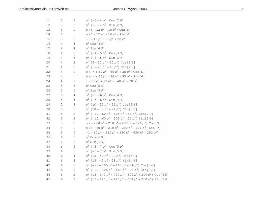
11 3 2 ρ2 H−3 + 4 ρ2L Cos@2 θD12 3 2 ρ2 H−3 + 4 ρ2L Sin@2 θD13 3 1 ρ H3 − 12 ρ2 + 10 ρ4L Cos@θD14 3 1 ρ H3 − 12 ρ2 + 10 ρ4L Sin@θD15 3 0 −1 + 12 ρ2 − 30 ρ4 + 20 ρ6
16 4 4 ρ4 Cos@4 θD17 4 4 ρ4 Sin@4 θD18 4 3 ρ3 H−4 + 5 ρ2L Cos@3 θD19 4 3 ρ3 H−4 + 5 ρ2L Sin@3 θD20 4 2 ρ2 H6 − 20 ρ2 + 15 ρ4L Cos@2 θD21 4 2 ρ2 H6 − 20 ρ2 + 15 ρ4L Sin@2 θD22 4 1 ρ H−4 + 30 ρ2 − 60 ρ4 + 35 ρ6L Cos@θD23 4 1 ρ H−4 + 30 ρ2 − 60 ρ4 + 35 ρ6L Sin@θD24 4 0 1 − 20 ρ2 + 90 ρ4 − 140 ρ6 + 70 ρ8
25 5 5 ρ5 Cos@5 θD26 5 5 ρ5 Sin@5 θD27 5 4 ρ4 H−5 + 6 ρ2L Cos@4 θD28 5 4 ρ4 H−5 + 6 ρ2L Sin@4 θD29 5 3 ρ3 H10 − 30 ρ2 + 21 ρ4L Cos@3 θD30 5 3 ρ3 H10 − 30 ρ2 + 21 ρ4L Sin@3 θD31 5 2 ρ2 H−10 + 60 ρ2 − 105 ρ4 + 56 ρ6L Cos@2 θD32 5 2 ρ2 H−10 + 60 ρ2 − 105 ρ4 + 56 ρ6L Sin@2 θD33 5 1 ρ H5 − 60 ρ2 + 210 ρ4 − 280 ρ6 + 126 ρ8L Cos@θD34 5 1 ρ H5 − 60 ρ2 + 210 ρ4 − 280 ρ6 + 126 ρ8L Sin@θD35 5 0 −1 + 30 ρ2 − 210 ρ4 + 560 ρ6 − 630 ρ8 + 252 ρ10
36 6 6 ρ6 Cos@6 θD37 6 6 ρ6 Sin@6 θD38 6 5 ρ5 H−6 + 7 ρ2L Cos@5 θD39 6 5 ρ5 H−6 + 7 ρ2L Sin@5 θD40 6 4 ρ4 H15 − 42 ρ2 + 28 ρ4L Cos@4 θD41 6 4 ρ4 H15 − 42 ρ2 + 28 ρ4L Sin@4 θD42 6 3 ρ3 H−20 + 105 ρ2 − 168 ρ4 + 84 ρ6L Cos@3 θD43 6 3 ρ3 H−20 + 105 ρ2 − 168 ρ4 + 84 ρ6L Sin@3 θD44 6 2 ρ2 H15 − 140 ρ2 + 420 ρ4 − 504 ρ6 + 210 ρ8L Cos@2 θD45 6 2 ρ2 H15 − 140 ρ2 + 420 ρ4 − 504 ρ6 + 210 ρ8L Sin@2 θD
ZernikePolynomialsForTheWeb.nb James C. Wyant, 2003 4
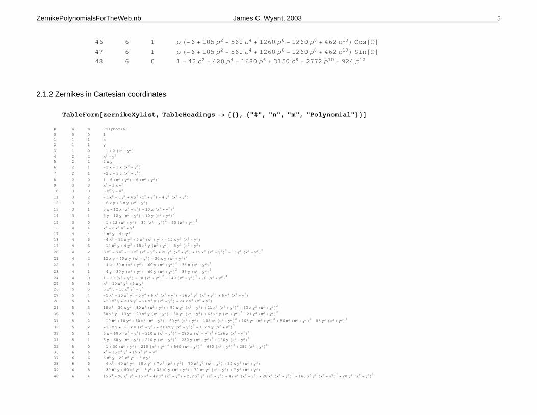
46 6 1 ρ H−6 + 105 ρ2 − 560 ρ4 + 1260 ρ6 − 1260 ρ8 + 462 ρ10L Cos@θD47 6 1 ρ H−6 + 105 ρ2 − 560 ρ4 + 1260 ρ6 − 1260 ρ8 + 462 ρ10L Sin@θD48 6 0 1 − 42 ρ2 + 420 ρ4 − 1680 ρ6 + 3150 ρ8 − 2772 ρ10 + 924 ρ12
2.1.2 Zernikes in Cartesian coordinates
TableForm@zernikeXyList, TableHeadings −> 88<, 8"#", "n", "m", "Polynomial"<<D# n m Polynomial0 0 0 11 1 1 x2 1 1 y3 1 0 −1 + 2 Hx2 + y2L4 2 2 x2 − y2
5 2 2 2 x y6 2 1 −2 x + 3 x Hx2 + y2L7 2 1 −2 y + 3 y Hx2 + y2L8 2 0 1 − 6 Hx2 + y2L + 6 Hx2 + y2L2
9 3 3 x3 − 3 x y2
10 3 3 3 x2 y − y3
11 3 2 −3 x2 + 3 y2 + 4 x2 Hx2 + y2L − 4 y2 Hx2 + y2L12 3 2 −6 x y + 8 x y Hx2 + y2L13 3 1 3 x − 12 x Hx2 + y2L + 10 x Hx2 + y2L2
14 3 1 3 y − 12 y Hx2 + y2L + 10 y Hx2 + y2L2
15 3 0 −1 + 12 Hx2 + y2L − 30 Hx2 + y2L2+ 20 Hx2 + y2L3
16 4 4 x4 − 6 x2 y2 + y4
17 4 4 4 x3 y − 4 x y3
18 4 3 −4 x3 + 12 x y2 + 5 x3 Hx2 + y2L − 15 x y2 Hx2 + y2L19 4 3 −12 x2 y + 4 y3 + 15 x2 y Hx2 + y2L − 5 y3 Hx2 + y2L20 4 2 6 x2 − 6 y2 − 20 x2 Hx2 + y2L + 20 y2 Hx2 + y2L + 15 x2 Hx2 + y2L2
− 15 y2 Hx2 + y2L2
21 4 2 12 x y − 40 x y Hx2 + y2L + 30 x y Hx2 + y2L2
22 4 1 −4 x + 30 x Hx2 + y2L − 60 x Hx2 + y2L2+ 35 x Hx2 + y2L3
23 4 1 −4 y + 30 y Hx2 + y2L − 60 y Hx2 + y2L2+ 35 y Hx2 + y2L3
24 4 0 1 − 20 Hx2 + y2L + 90 Hx2 + y2L2− 140 Hx2 + y2L3
+ 70 Hx2 + y2L4
25 5 5 x5 − 10 x3 y2 + 5 x y4
26 5 5 5 x4 y − 10 x2 y3 + y5
27 5 4 −5 x4 + 30 x2 y2 − 5 y4 + 6 x4 Hx2 + y2L − 36 x2 y2 Hx2 + y2L + 6 y4 Hx2 + y2L28 5 4 −20 x3 y + 20 x y3 + 24 x3 y Hx2 + y2L − 24 x y3 Hx2 + y2L29 5 3 10 x3 − 30 x y2 − 30 x3 Hx2 + y2L + 90 x y2 Hx2 + y2L + 21 x3 Hx2 + y2L2
− 63 x y2 Hx2 + y2L2
30 5 3 30 x2 y − 10 y3 − 90 x2 y Hx2 + y2L + 30 y3 Hx2 + y2L + 63 x2 y Hx2 + y2L2− 21 y3 Hx2 + y2L2
31 5 2 −10 x2 + 10 y2 + 60 x2 Hx2 + y2L − 60 y2 Hx2 + y2L − 105 x2 Hx2 + y2L2+ 105 y2 Hx2 + y2L2
+ 56 x2 Hx2 + y2L3− 56 y2 Hx2 + y2L3
32 5 2 −20 x y + 120 x y Hx2 + y2L − 210 x y Hx2 + y2L2+ 112 x y Hx2 + y2L3
33 5 1 5 x − 60 x Hx2 + y2L + 210 x Hx2 + y2L2− 280 x Hx2 + y2L3
+ 126 x Hx2 + y2L4
34 5 1 5 y − 60 y Hx2 + y2L + 210 y Hx2 + y2L2− 280 y Hx2 + y2L3
+ 126 y Hx2 + y2L4
35 5 0 −1 + 30 Hx2 + y2L − 210 Hx2 + y2L2+ 560 Hx2 + y2L3
− 630 Hx2 + y2L4+ 252 Hx2 + y2L5
36 6 6 x6 − 15 x4 y2 + 15 x2 y4 − y6
37 6 6 6 x5 y − 20 x3 y3 + 6 x y5
38 6 5 −6 x5 + 60 x3 y2 − 30 x y4 + 7 x5 Hx2 + y2L − 70 x3 y2 Hx2 + y2L + 35 x y4 Hx2 + y2L39 6 5 −30 x4 y + 60 x2 y3 − 6 y5 + 35 x4 y Hx2 + y2L − 70 x2 y3 Hx2 + y2L + 7 y5 Hx2 + y2L40 6 4 15 x4 − 90 x2 y2 + 15 y4 − 42 x4 Hx2 + y2L + 252 x2 y2 Hx2 + y2L − 42 y4 Hx2 + y2L + 28 x4 Hx2 + y2L2
− 168 x2 y2 Hx2 + y2L2+ 28 y4 Hx2 + y2L2
ZernikePolynomialsForTheWeb.nb James C. Wyant, 2003 5
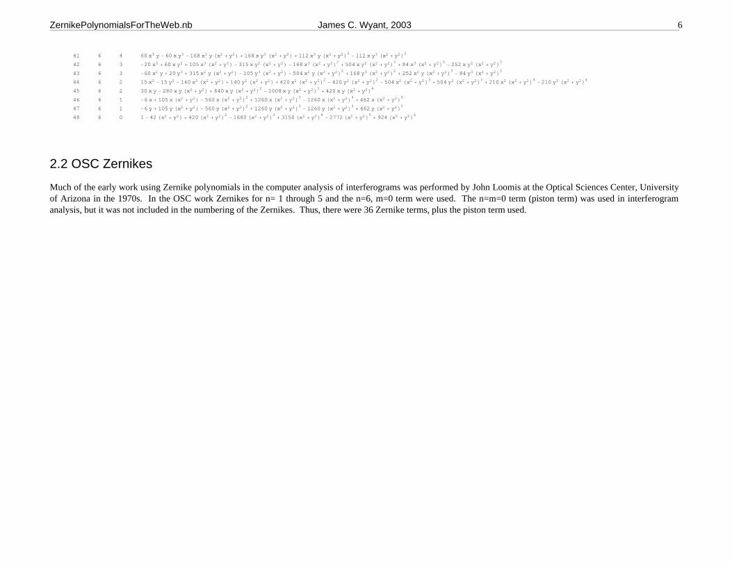
41 6 4 60 x3 y − 60 x y3 − 168 x3 y Hx2 + y2L + 168 x y3 Hx2 + y2L + 112 x3 y Hx2 + y2L2− 112 x y3 Hx2 + y2L2
42 6 3 −20 x3 + 60 x y2 + 105 x3 Hx2 + y2L − 315 x y2 Hx2 + y2L − 168 x3 Hx2 + y2L2+ 504 x y2 Hx2 + y2L2
+ 84 x3 Hx2 + y2L3− 252 x y2 Hx2 + y2L3
43 6 3 −60 x2 y + 20 y3 + 315 x2 y Hx2 + y2L − 105 y3 Hx2 + y2L − 504 x2 y Hx2 + y2L2+ 168 y3 Hx2 + y2L2
+ 252 x2 y Hx2 + y2L3− 84 y3 Hx2 + y2L3
44 6 2 15 x2 − 15 y2 − 140 x2 Hx2 + y2L + 140 y2 Hx2 + y2L + 420 x2 Hx2 + y2L2− 420 y2 Hx2 + y2L2
− 504 x2 Hx2 + y2L3+ 504 y2 Hx2 + y2L3
+ 210 x2 Hx2 + y2L4− 210 y2 Hx2 + y2L4
45 6 2 30 x y − 280 x y Hx2 + y2L + 840 x y Hx2 + y2L2− 1008 x y Hx2 + y2L3
+ 420 x y Hx2 + y2L4
46 6 1 −6 x + 105 x Hx2 + y2L − 560 x Hx2 + y2L2+ 1260 x Hx2 + y2L3
− 1260 x Hx2 + y2L4+ 462 x Hx2 + y2L5
47 6 1 −6 y + 105 y Hx2 + y2L − 560 y Hx2 + y2L2+ 1260 y Hx2 + y2L3
− 1260 y Hx2 + y2L4+ 462 y Hx2 + y2L5
48 6 0 1 − 42 Hx2 + y2L + 420 Hx2 + y2L2− 1680 Hx2 + y2L3
+ 3150 Hx2 + y2L4− 2772 Hx2 + y2L5
+ 924 Hx2 + y2L6
2.2 OSC Zernikes
Much of the early work using Zernike polynomials in the computer analysis of interferograms was performed by John Loomis at the Optical Sciences Center, Universityof Arizona in the 1970s. In the OSC work Zernikes for n= 1 through 5 and the n=6, m=0 term were used. The n=m=0 term (piston term) was used in interferogramanalysis, but it was not included in the numbering of the Zernikes. Thus, there were 36 Zernike terms, plus the piston term used.
ZernikePolynomialsForTheWeb.nb James C. Wyant, 2003 6
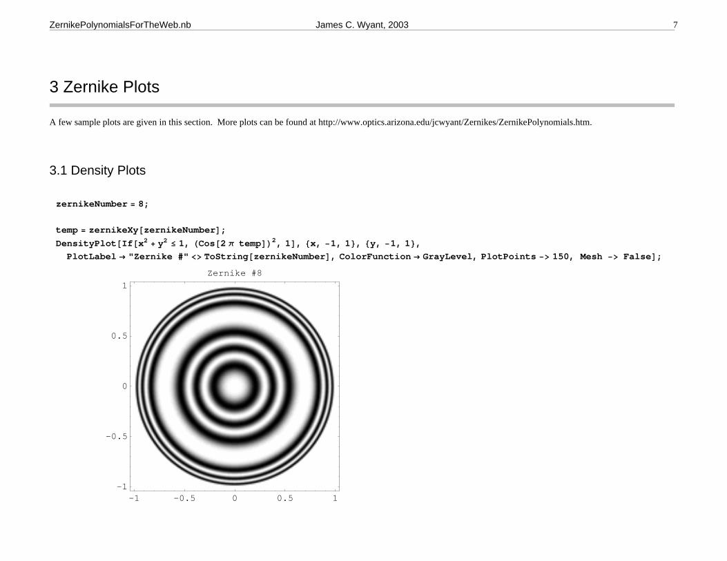
3 Zernike Plots
A few sample plots are given in this section. More plots can be found at http://www.optics.arizona.edu/jcwyant/Zernikes/ZernikePolynomials.htm.
3.1 Density Plots
zernikeNumber = 8;
temp = zernikeXy@zernikeNumberD;DensityPlot@If@x2 + y2 ≤ 1, HCos@2 π tempDL2, 1D, 8x, −1, 1<, 8y, −1, 1<,
PlotLabel → "Zernike #" <> ToString@zernikeNumberD, ColorFunction → GrayLevel, PlotPoints −> 150, Mesh −> FalseD;
-1 -0.5 0 0.5 1-1
-0.5
0
0.5
1Zernike #8
ZernikePolynomialsForTheWeb.nb James C. Wyant, 2003 7
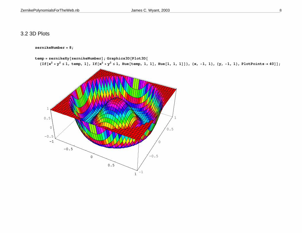
3.2 3D Plots
zernikeNumber = 8;
temp = zernikeXy@zernikeNumberD; Graphics3D@Plot3D@8If@x2 + y2 ≤ 1, temp, 1D, If@x2 + y2 ≤ 1, Hue@temp, 1, 1D, Hue@1, 1, 1DD<, 8x, −1, 1<, 8y, −1, 1<, PlotPoints → 40DD;
-1
-0.5
0
0.5
1 -1
-0.5
0
0.5
1
-0.5
0
0.5
1
-1
-0.5
0
0.5
1
ZernikePolynomialsForTheWeb.nb James C. Wyant, 2003 8
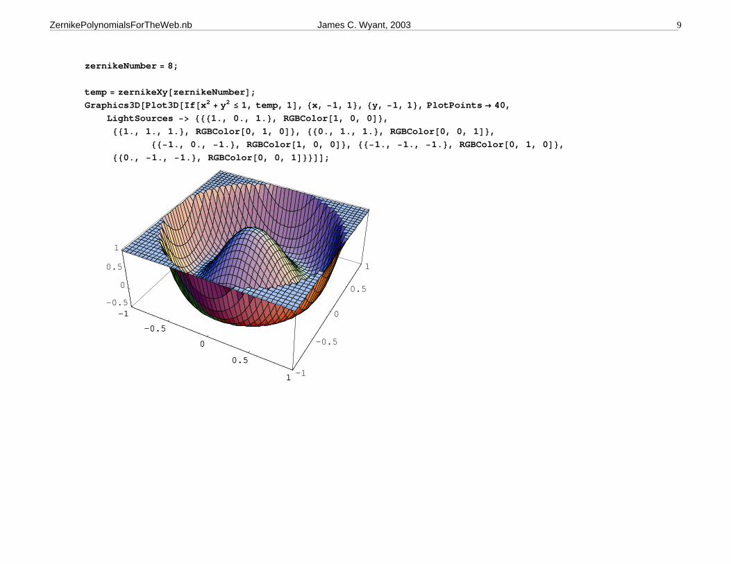
zernikeNumber = 8;
temp = zernikeXy@zernikeNumberD;Graphics3D@Plot3D@If@x2 + y2 ≤ 1, temp, 1D, 8x, −1, 1<, 8y, −1, 1<, PlotPoints → 40,
LightSources −> 8881., 0., 1.<, RGBColor@1, 0, 0D<,881., 1., 1.<, RGBColor@0, 1, 0D<, 880., 1., 1.<, RGBColor@0, 0, 1D<,
88−1., 0., −1.<, RGBColor@1, 0, 0D<, 88−1., −1., −1.<, RGBColor@0, 1, 0D<,880., −1., −1.<, RGBColor@0, 0, 1D<<DD;
-1
-0.5
0
0.5
1 -1
-0.5
0
0.5
1
-0.5
0
0.5
1
-1
-0.5
0
0.5
1
ZernikePolynomialsForTheWeb.nb James C. Wyant, 2003 9
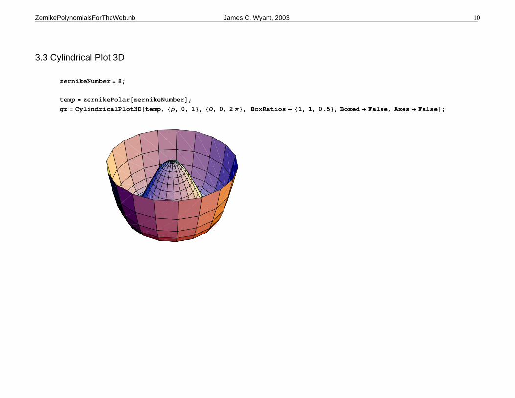
3.3 Cylindrical Plot 3D
zernikeNumber = 8;
temp = zernikePolar@zernikeNumberD;gr = CylindricalPlot3D@temp, 8ρ, 0, 1<, 8θ, 0, 2 π<, BoxRatios → 81, 1, 0.5<, Boxed → False, Axes → FalseD;
ZernikePolynomialsForTheWeb.nb James C. Wyant, 2003 10
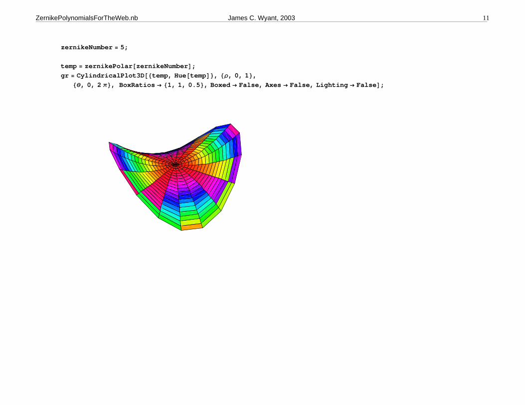
zernikeNumber = 5;
temp = zernikePolar@zernikeNumberD;gr = CylindricalPlot3D@8temp, Hue@tempD<, 8ρ, 0, 1<,
8θ, 0, 2 π<, BoxRatios → 81, 1, 0.5<, Boxed → False, Axes → False, Lighting → FalseD;
ZernikePolynomialsForTheWeb.nb James C. Wyant, 2003 11
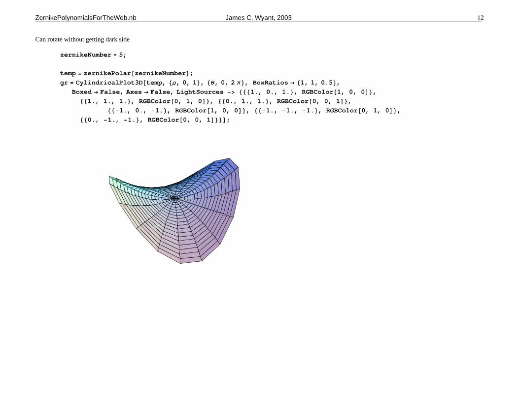
Can rotate without getting dark side
zernikeNumber = 5;
temp = zernikePolar@zernikeNumberD;gr = CylindricalPlot3D@temp, 8ρ, 0, 1<, 8θ, 0, 2 π<, BoxRatios → 81, 1, 0.5<,
Boxed → False, Axes → False, LightSources −> 8881., 0., 1.<, RGBColor@1, 0, 0D<,881., 1., 1.<, RGBColor@0, 1, 0D<, 880., 1., 1.<, RGBColor@0, 0, 1D<,
88−1., 0., −1.<, RGBColor@1, 0, 0D<, 88−1., −1., −1.<, RGBColor@0, 1, 0D<,880., −1., −1.<, RGBColor@0, 0, 1D<<D;
ZernikePolynomialsForTheWeb.nb James C. Wyant, 2003 12
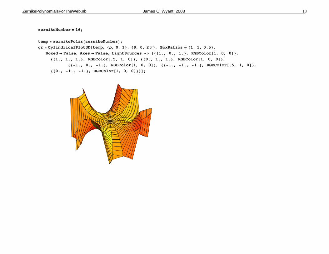
zernikeNumber = 16;
temp = zernikePolar@zernikeNumberD;gr = CylindricalPlot3D@temp, 8ρ, 0, 1<, 8θ, 0, 2 π<, BoxRatios → 81, 1, 0.5<,
Boxed → False, Axes → False, LightSources −> 8881., 0., 1.<, RGBColor@1, 0, 0D<,881., 1., 1.<, [email protected], 1, 0D<, 880., 1., 1.<, RGBColor@1, 0, 0D<,
88−1., 0., −1.<, RGBColor@1, 0, 0D<, 88−1., −1., −1.<, [email protected], 1, 0D<,880., −1., −1.<, RGBColor@1, 0, 0D<<D;
ZernikePolynomialsForTheWeb.nb James C. Wyant, 2003 13
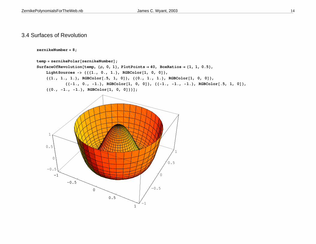
3.4 Surfaces of Revolution
zernikeNumber = 8;
temp = zernikePolar@zernikeNumberD;SurfaceOfRevolution@temp, 8ρ, 0, 1<, PlotPoints → 40, BoxRatios → 81, 1, 0.5<,
LightSources −> 8881., 0., 1.<, RGBColor@1, 0, 0D<,881., 1., 1.<, [email protected], 1, 0D<, 880., 1., 1.<, RGBColor@1, 0, 0D<,
88−1., 0., −1.<, RGBColor@1, 0, 0D<, 88−1., −1., −1.<, [email protected], 1, 0D<,880., −1., −1.<, RGBColor@1, 0, 0D<<D;
-1
-0.5
0
0.5
1-1
-0.5
0
0.5
1
-0.5
0
0.5
1
-1
-0.5
0
0.5
1
ZernikePolynomialsForTheWeb.nb James C. Wyant, 2003 14
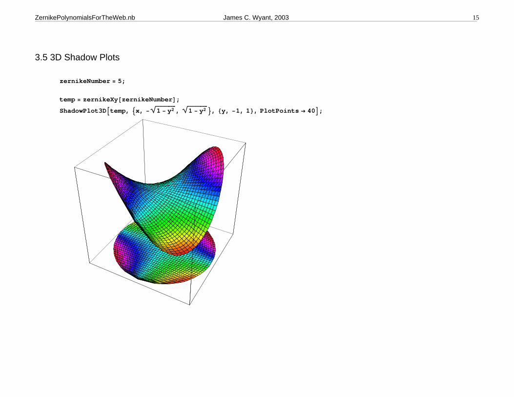
3.5 3D Shadow Plots
zernikeNumber = 5;
temp = zernikeXy@zernikeNumberD;
ShadowPlot3DAtemp, 9x, −è!!!!!!!!!!!!!
1 − y2 ,è!!!!!!!!!!!!!
1 − y2 =, 8y, −1, 1<, PlotPoints → 40E;
ZernikePolynomialsForTheWeb.nb James C. Wyant, 2003 15
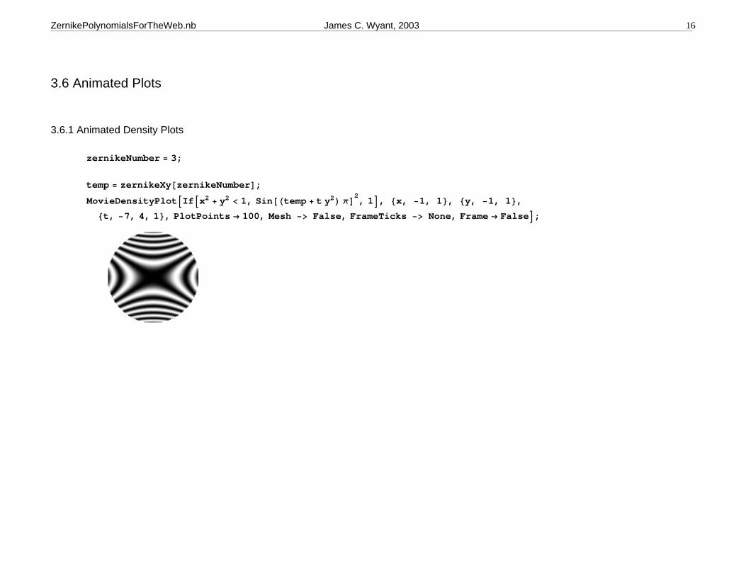
3.6 Animated Plots
3.6.1 Animated Density Plots
zernikeNumber = 3;
temp = zernikeXy@zernikeNumberD;
MovieDensityPlotAIfAx2 + y2 < 1, Sin@Htemp + t y2L πD2, 1E, 8x, −1, 1<, 8y, −1, 1<,
8t, −7, 4, 1<, PlotPoints → 100, Mesh −> False, FrameTicks −> None, Frame → FalseE;
ZernikePolynomialsForTheWeb.nb James C. Wyant, 2003 16
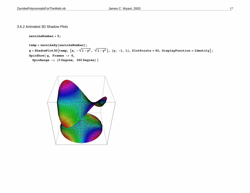
3.6.2 Animated 3D Shadow Plots
zernikeNumber = 5;
temp = zernikeXy@zernikeNumberD;
g = ShadowPlot3DAtemp, 9x, −è!!!!!!!!!!!!!
1 − y2 ,è!!!!!!!!!!!!!
1 − y2 =, 8y, −1, 1<, PlotPoints → 40, DisplayFunction → IdentityE;
SpinShow@ g, Frames −> 6,SpinRange −> 80 Degree, 360 Degree< D
ZernikePolynomialsForTheWeb.nb James C. Wyant, 2003 17
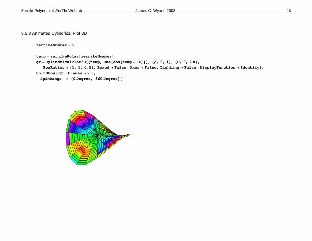
3.6.3 Animated Cylindrical Plot 3D
zernikeNumber = 5;
temp = zernikePolar@zernikeNumberD;gr = CylindricalPlot3D@8temp, Hue@Abs@temp + .4DD<, 8ρ, 0, 1<, 8θ, 0, 2 π<,
BoxRatios → 81, 1, 0.5<, Boxed → False, Axes → False, Lighting → False, DisplayFunction → IdentityD;SpinShow@ gr, Frames −> 6,
SpinRange −> 80 Degree, 360 Degree< D
ZernikePolynomialsForTheWeb.nb James C. Wyant, 2003 18
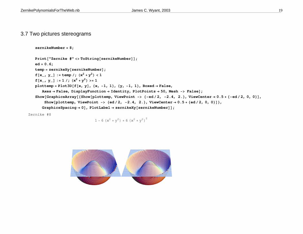
3.7 Two pictures stereograms
zernikeNumber = 8;
Print@"Zernike #" <> ToString@zernikeNumberDD;ed = 0.6;temp = zernikeXy@zernikeNumberD;f@x_, y_D := temp ê; Hx2 + y2L < 1f@x_, y_D := 1 ê; Hx2 + y2L >= 1plottemp = Plot3D@f@x, yD, 8x, −1, 1<, 8y, −1, 1<, Boxed → False,
Axes → False, DisplayFunction → Identity, PlotPoints → 50, Mesh −> FalseD;Show@GraphicsArray@8Show@plottemp, ViewPoint −> 8−ed ê2, −2.4, 2.<, ViewCenter → 0.5 + 8−ed ê2, 0, 0<D,
Show@plottemp, ViewPoint −> 8ed ê2, −2.4, 2.<, ViewCenter → 0.5 + 8ed ê2, 0, 0<D<,GraphicsSpacing → 0D, PlotLabel → zernikeXy@zernikeNumberDD;
Zernike #8
1 − 6 Hx2 + y2L + 6 Hx2 + y2L2
ZernikePolynomialsForTheWeb.nb James C. Wyant, 2003 19
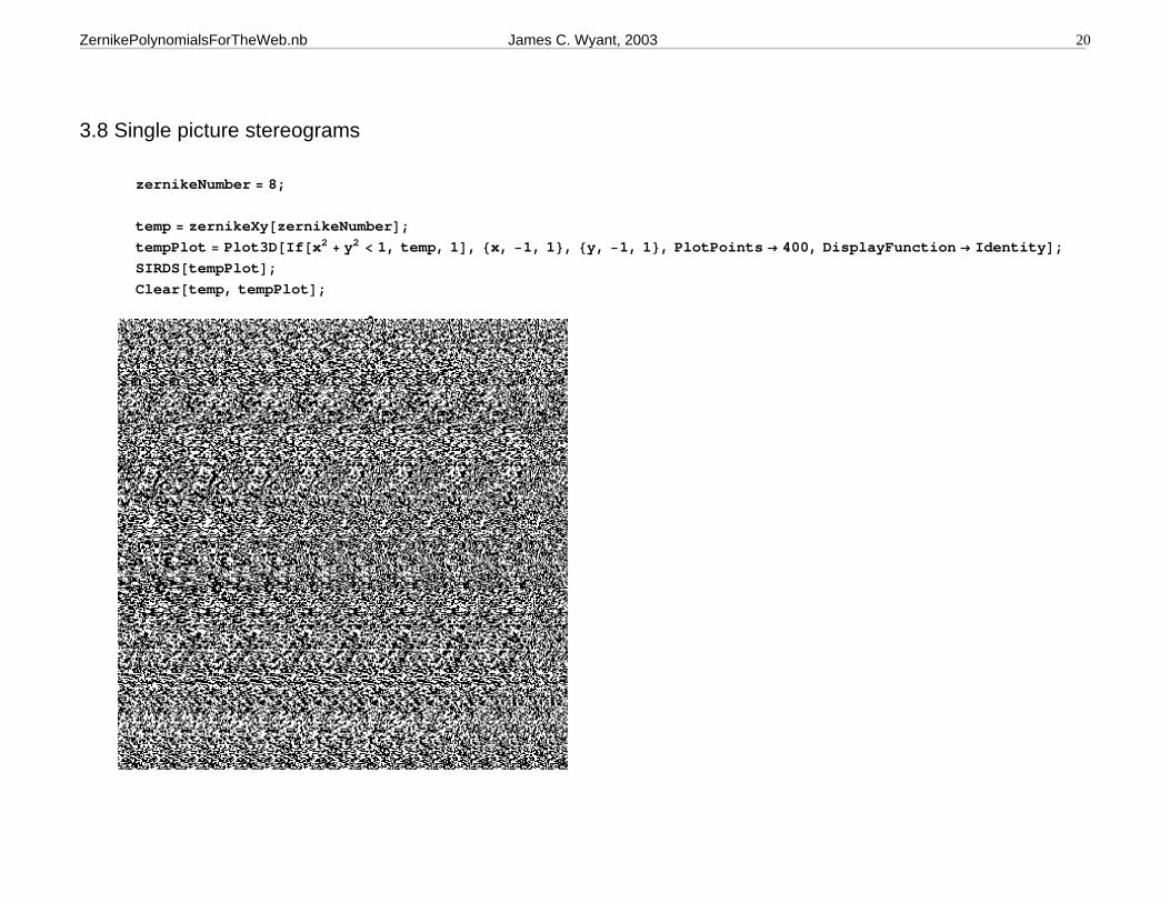
3.8 Single picture stereograms
zernikeNumber = 8;
temp = zernikeXy@zernikeNumberD;tempPlot = Plot3D@If@x2 + y2 < 1, temp, 1D, 8x, −1, 1<, 8y, −1, 1<, PlotPoints → 400, DisplayFunction → IdentityD;SIRDS@tempPlotD;Clear@temp, tempPlotD;
ZernikePolynomialsForTheWeb.nb James C. Wyant, 2003 20
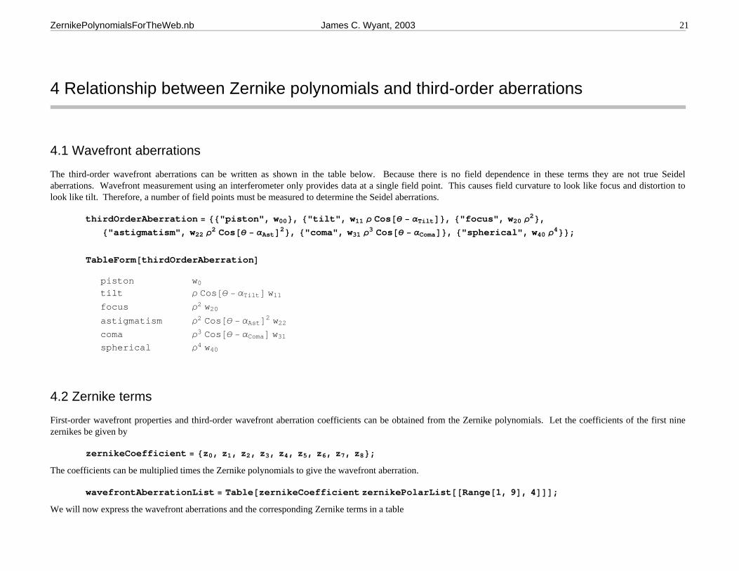
4 Relationship between Zernike polynomials and third-order aberrations
4.1 Wavefront aberrations
The third-order wavefront aberrations can be written as shown in the table below. Because there is no field dependence in these terms they are not true Seidelaberrations. Wavefront measurement using an interferometer only provides data at a single field point. This causes field curvature to look like focus and distortion tolook like tilt. Therefore, a number of field points must be measured to determine the Seidel aberrations.
thirdOrderAberration = 88"piston", w00<, 8"tilt", w11 ρ Cos@θ − αTiltD<, 8"focus", w20 ρ2<,8"astigmatism", w22 ρ2 Cos@θ − αAstD2<, 8"coma", w31 ρ3 Cos@θ − αComaD<, 8"spherical", w40 ρ4<<;
TableForm@thirdOrderAberrationD
piston w0
tilt ρ Cos@θ − αTiltD w11
focus ρ2 w20
astigmatism ρ2 Cos@θ − αAstD2 w22
coma ρ3 Cos@θ − αComaD w31
spherical ρ4 w40
4.2 Zernike terms
First-order wavefront properties and third-order wavefront aberration coefficients can be obtained from the Zernike polynomials. Let the coefficients of the first ninezernikes be given by
zernikeCoefficient = 8z0, z1, z2, z3, z4, z5, z6, z7, z8<;
The coefficients can be multiplied times the Zernike polynomials to give the wavefront aberration.
wavefrontAberrationList = Table@zernikeCoefficient zernikePolarList@@Range@1, 9D, 4DDD;
We will now express the wavefront aberrations and the corresponding Zernike terms in a table
ZernikePolynomialsForTheWeb.nb James C. Wyant, 2003 21
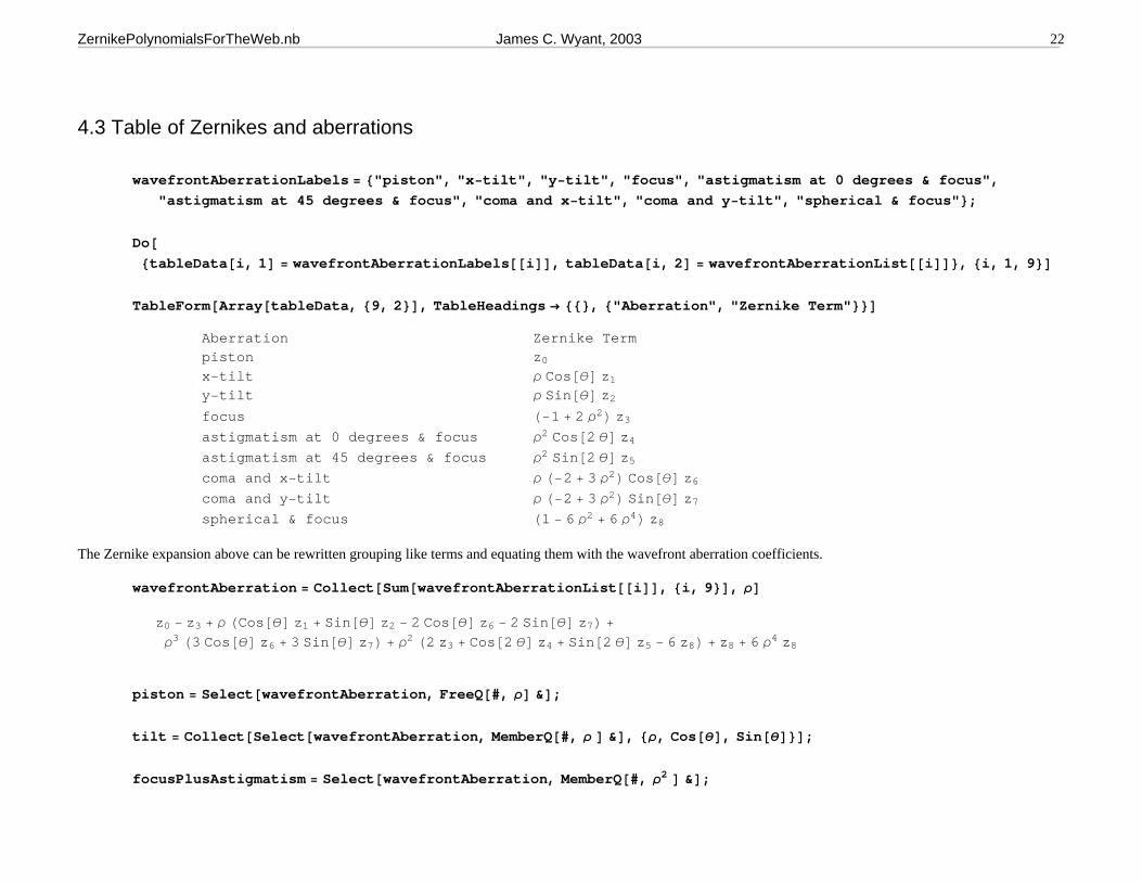
4.3 Table of Zernikes and aberrations
wavefrontAberrationLabels = 8"piston", "x−tilt", "y−tilt", "focus", "astigmatism at 0 degrees & focus","astigmatism at 45 degrees & focus", "coma and x−tilt", "coma and y−tilt", "spherical & focus"<;
Do@8tableData@i, 1D = wavefrontAberrationLabels@@iDD, tableData@i, 2D = wavefrontAberrationList@@iDD<, 8i, 1, 9<D
TableForm@Array@tableData, 89, 2<D, TableHeadings → 88<, 8"Aberration", "Zernike Term"<<D
Aberration Zernike Termpiston z0
x−tilt ρ Cos@θD z1
y−tilt ρ Sin@θD z2
focus H−1 + 2 ρ2L z3
astigmatism at 0 degrees & focus ρ2 Cos@2 θD z4
astigmatism at 45 degrees & focus ρ2 Sin@2 θD z5
coma and x−tilt ρ H−2 + 3 ρ2L Cos@θD z6
coma and y−tilt ρ H−2 + 3 ρ2L Sin@θD z7
spherical & focus H1 − 6 ρ2 + 6 ρ4L z8
The Zernike expansion above can be rewritten grouping like terms and equating them with the wavefront aberration coefficients.
wavefrontAberration = Collect@Sum@wavefrontAberrationList@@iDD, 8i, 9<D, ρD
z0 − z3 + ρ HCos@θD z1 + Sin@θD z2 − 2 Cos@θD z6 − 2 Sin@θD z7L +
ρ3 H3 Cos@θD z6 + 3 Sin@θD z7L + ρ2 H2 z3 + Cos@2 θD z4 + Sin@2 θD z5 − 6 z8L + z8 + 6 ρ4 z8
piston = Select@wavefrontAberration, FreeQ@#, ρD &D;
tilt = Collect@Select@wavefrontAberration, MemberQ@#, ρ D &D, 8ρ, Cos@θD, Sin@θD<D;
focusPlusAstigmatism = Select@wavefrontAberration, MemberQ@#, ρ2 D &D;
ZernikePolynomialsForTheWeb.nb James C. Wyant, 2003 22

coma = Select@wavefrontAberration, MemberQ@#, ρ3 D &D;
spherical = Select@wavefrontAberration, MemberQ@#, ρ4 D &D;
4.4 zernikeThirdOrderAberration Table
zernikeThirdOrderAberration = 88"piston", piston<, 8"tilt", tilt<,8"focus + astigmatism", focusPlusAstigmatism<, 8"coma", coma<, 8"spherical", spherical<<;
TableForm@zernikeThirdOrderAberrationD
piston z0 − z3 + z8
tilt ρ HCos@θD Hz1 − 2 z6L + Sin@θD Hz2 − 2 z7LLfocus + astigmatism ρ2 H2 z3 + Cos@2 θD z4 + Sin@2 θD z5 − 6 z8Lcoma ρ3 H3 Cos@θD z6 + 3 Sin@θD z7Lspherical 6 ρ4 z8
These tilt, coma, and focus plus astigmatism terms can be rearranged using the equationa Cos@θD + b Sin@θD =
è!!!!!!!!!!!!!!!a2 + b2 Cos@θ − ArcTan@a, bDD.
4.4.1 Tilt
tilt = tilt ê. a_ Cos@θ_D + b_ Sin@θD →è!!!!!!!!!!!!!!!
a2 + b2 Cos@θ − ArcTan@a, bDD
ρ Cos@θ − ArcTan@z1 − 2 z6, z2 − 2 z7DD "#######################################################Hz1 − 2 z6L2 + Hz2 − 2 z7L2
4.4.2 Coma
coma = SimplifyAcoma ê. a_ Cos@θ_D + b_ Sin@θD →è!!!!!!!!!!!!!!!
a2 + b2 Cos@θ − ArcTan@a, bDDE
ZernikePolynomialsForTheWeb.nb James C. Wyant, 2003 23
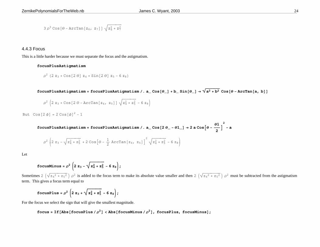
3 ρ3 Cos@θ − ArcTan@z6, z7DD "###############z62 + z7
2
4.4.3 Focus
This is a little harder because we must separate the focus and the astigmatism.
focusPlusAstigmatism
ρ2 H2 z3 + Cos@2 θD z4 + Sin@2 θD z5 − 6 z8L
focusPlusAstigmatism = focusPlusAstigmatism ê. a_ Cos@θ_D + b_ Sin@θ_D →è!!!!!!!!!!!!!!!
a2 + b2 Cos@θ − ArcTan@a, bDD
ρ2 J2 z3 + Cos@2 θ − ArcTan@z4, z5DD "###############z42 + z5
2 − 6 z8N
But Cos@2 φD = 2 Cos@φD2 − 1
focusPlusAstigmatism = focusPlusAstigmatism ê. a_ Cos@2 θ_ − θ1_D → 2 a CosAθ −θ1
2E
2
− a
ρ2 ikjjj2 z3 − "###############z4
2 + z52 + 2 CosAθ −
12
ArcTan@z4, z5DE2 "###############z4
2 + z52 − 6 z8
y{zzz
Let
focusMinus = ρ2 ikjj2 z3 −
"###############z4
2 + z52 − 6 z8
y{zz;
Sometimes 2 Iè!!!!!!!!!!!!!!!!!!!z42 + z52 M ρ2 is added to the focus term to make its absolute value smaller and then 2 Iè!!!!!!!!!!!!!!!!!!!z42 + z52 M ρ2 must be subtracted from the astigmatismterm. This gives a focus term equal to
focusPlus = ρ2 ikjj2 z3 +
"###############z4
2 + z52 − 6 z8
y{zz;
For the focus we select the sign that will give the smallest magnitude.
focus = If@Abs@focusPlusêρ2D < Abs@focusMinusêρ2D, focusPlus, focusMinusD;
ZernikePolynomialsForTheWeb.nb James C. Wyant, 2003 24
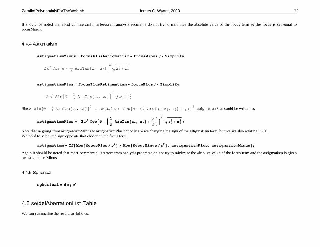
It should be noted that most commercial interferogram analysis programs do not try to minimize the absolute valus of the focus term so the focus is set equal tofocusMinus.
4.4.4 Astigmatism
astigmatismMinus = focusPlusAstigmatism − focusMinus êê Simplify
2 ρ2 CosAθ −12
ArcTan@z4, z5DE2 "###############z4
2 + z52
astigmatismPlus = focusPlusAstigmatism − focusPlus êê Simplify
−2 ρ2 SinAθ −12
ArcTan@z4, z5DE2 "###############z4
2 + z52
Since Sin@θ − 12 ArcTan@z4, z5DD2
is equal to Cos@θ − H 12 ArcTan@z4, z5D + π
2 LD2 , astigmatismPlus could be written as
astigmatismPlus = −2 ρ2 CosAθ − ikjjj
1
2ArcTan@z4, z5D +
π
2y{zzzE
2 "###############z4
2 + z52 ;
Note that in going from astigmatismMinus to astigmatismPlus not only are we changing the sign of the astigmatism term, but we are also rotating it 90°.We need to select the sign opposite that chosen in the focus term.
astigmatism = If@Abs@focusPlusêρ2D < Abs@focusMinusêρ2D, astigmatismPlus, astigmatismMinusD;
Again it should be noted that most commercial interferogram analysis programs do not try to minimize the absolute valus of the focus term and the astigmatism is givenby astigmatismMinus.
4.4.5 Spherical
spherical = 6 z8 ρ4
4.5 seidelAberrationList Table
We can summarize the results as follows.
ZernikePolynomialsForTheWeb.nb James C. Wyant, 2003 25
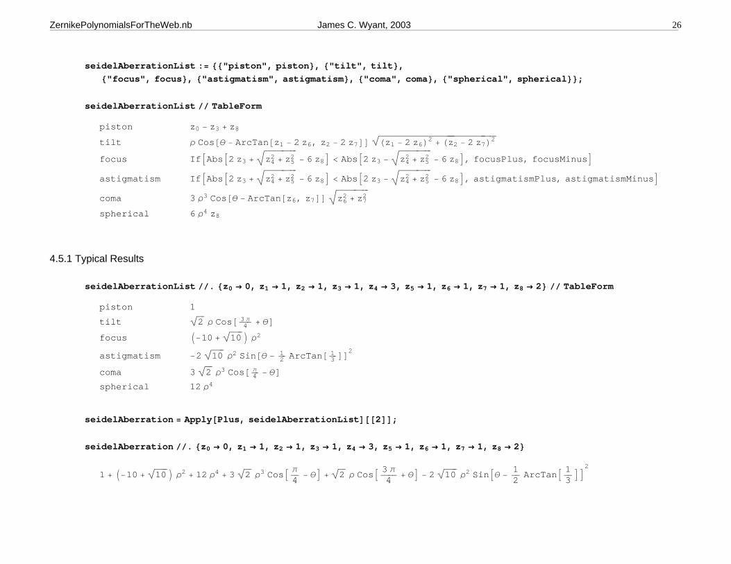
seidelAberrationList := 88"piston", piston<, 8"tilt", tilt<,8"focus", focus<, 8"astigmatism", astigmatism<, 8"coma", coma<, 8"spherical", spherical<<;
seidelAberrationList êê TableForm
piston z0 − z3 + z8
tilt ρ Cos@θ − ArcTan@z1 − 2 z6, z2 − 2 z7DD è!!!!!!!!!!!!!!!!!!!!!!!!!!!!!!!!!!!!!!!!!!!!!!!!!!!!!!!Hz1 − 2 z6L2 + Hz2 − 2 z7L2
focus IfAAbsA2 z3 + "###############z42 + z5
2 − 6 z8E < AbsA2 z3 − "###############z42 + z5
2 − 6 z8E, focusPlus, focusMinusE
astigmatism IfAAbsA2 z3 + "###############z42 + z5
2 − 6 z8E < AbsA2 z3 − "###############z42 + z5
2 − 6 z8E, astigmatismPlus, astigmatismMinusE
coma 3 ρ3 Cos@θ − ArcTan@z6, z7DD "###############z62 + z7
2
spherical 6 ρ4 z8
4.5.1 Typical Results
seidelAberrationList êê. 8z0 → 0, z1 → 1, z2 → 1, z3 → 1, z4 → 3, z5 → 1, z6 → 1, z7 → 1, z8 → 2< êê TableForm
piston 1
tilt è!!!2 ρ Cos@ 3 π4 + θD
focus I−10 +è!!!!!!10 M ρ2
astigmatism −2 è!!!!!!10 ρ2 Sin@θ − 12 ArcTan@ 1
3 DD2
coma 3 è!!!2 ρ3 Cos@ π4 − θD
spherical 12 ρ4
seidelAberration = Apply@Plus, seidelAberrationListD@@2DD;
seidelAberration êê. 8z0 → 0, z1 → 1, z2 → 1, z3 → 1, z4 → 3, z5 → 1, z6 → 1, z7 → 1, z8 → 2<
1 + I−10 +è!!!!!!10 M ρ2 + 12 ρ4 + 3 è!!!2 ρ3 CosA π
4− θE +
è!!!2 ρ CosA 3 π4
+ θE − 2 è!!!!!!10 ρ2 SinAθ −12
ArcTanA 13EE
2
ZernikePolynomialsForTheWeb.nb James C. Wyant, 2003 26
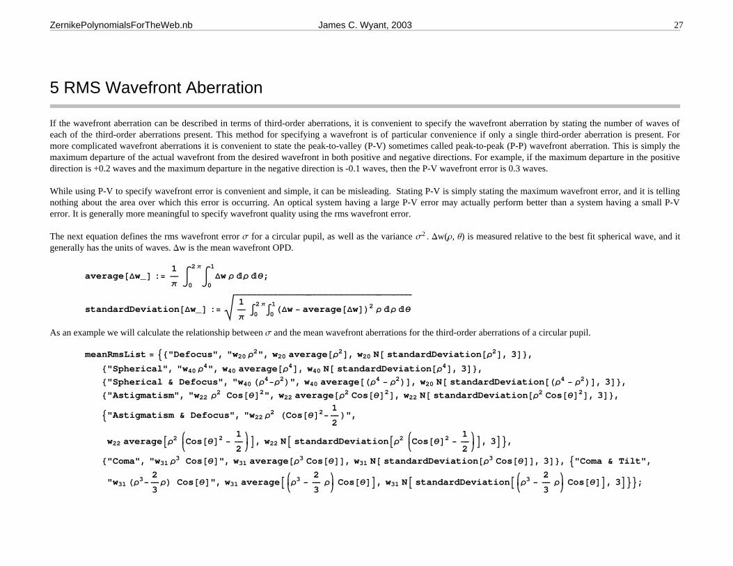
5 RMS Wavefront Aberration
If the wavefront aberration can be described in terms of third-order aberrations, it is convenient to specify the wavefront aberration by stating the number of waves ofeach of the third-order aberrations present. This method for specifying a wavefront is of particular convenience if only a single third-order aberration is present. Formore complicated wavefront aberrations it is convenient to state the peak-to-valley (P-V) sometimes called peak-to-peak (P-P) wavefront aberration. This is simply themaximum departure of the actual wavefront from the desired wavefront in both positive and negative directions. For example, if the maximum departure in the positivedirection is +0.2 waves and the maximum departure in the negative direction is -0.1 waves, then the P-V wavefront error is 0.3 waves.
While using P-V to specify wavefront error is convenient and simple, it can be misleading. Stating P-V is simply stating the maximum wavefront error, and it is tellingnothing about the area over which this error is occurring. An optical system having a large P-V error may actually perform better than a system having a small P-Verror. It is generally more meaningful to specify wavefront quality using the rms wavefront error.
The next equation defines the rms wavefront error s for a circular pupil, as well as the variance s2 . Dw(r, q) is measured relative to the best fit spherical wave, and itgenerally has the units of waves. Dw is the mean wavefront OPD.
average@∆w_D :=1
π ‡
0
2 π
‡0
1
∆w ρ ρ θ;
standardDeviation@∆w_D := $%%%%%%%%%%%%%%%%%%%%%%%%%%%%%%%%%%%%%%%%%%%%%%%%%%%%%%%%%%%%%%%%%%%%%%%%%%%%%%%%%1
π Ÿ0
2 πŸ0
1H∆w − average@∆wDL2 ρ ρ θ
As an example we will calculate the relationship between s and the mean wavefront aberrations for the third-order aberrations of a circular pupil.
meanRmsList = 98"Defocus", "w20 ρ2", w20 average@ρ2D, w20 N@ standardDeviation@ρ2D, 3D<,
8"Spherical", "w40 ρ4", w40 average@ρ4D, w40 N@ standardDeviation@ρ4D, 3D<,8"Spherical & Defocus", "w40 Hρ4−ρ2L", w40 average@Hρ4 − ρ2LD, w20 N@ standardDeviation@Hρ4 − ρ2LD, 3D<,8"Astigmatism", "w22 ρ2 Cos@θD2", w22 average@ρ2 Cos@θD2D, w22 N@ standardDeviation@ρ2 Cos@θD2D, 3D<,
9"Astigmatism & Defocus", "w22 ρ2 HCos@θD2−1
2L",
w22 averageAρ2 ikjjjCos@θD2 −
1
2y{zzzE, w22 NA standardDeviationAρ2 i
kjjjCos@θD2 −
1
2y{zzzE, 3E=,
8"Coma", "w31 ρ3 Cos@θD", w31 average@ρ3 Cos@θDD, w31 N@ standardDeviation@ρ3 Cos@θDD, 3D<, 9"Coma & Tilt",
"w31 Hρ3−2
3ρL Cos@θD", w31 averageAi
kjjjρ3 −
2
3 ρy{zzz Cos@θDE, w31 NA standardDeviationAi
kjjjρ3 −
2
3 ρy{zzz Cos@θDE, 3E==;
ZernikePolynomialsForTheWeb.nb James C. Wyant, 2003 27
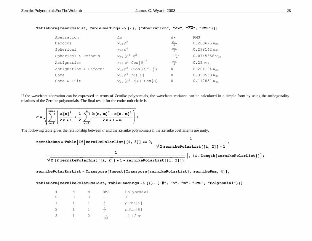
TableForm@meanRmsList, TableHeadings −> 88<, 8"Aberration", "∆w", "∆w¯¯
", "RMS"<<D
Aberration ∆w ∆w¯¯ RMS
Defocus w20 ρ2 w202 0.288675 w20
Spherical w40 ρ4 w403 0.298142 w40
Spherical & Defocus w40 Hρ4−ρ2L − w406 0.0745356 w20
Astigmatism w22 ρ2 Cos@θD2 w224 0.25 w22
Astigmatism & Defocus w22 ρ2 HCos@θD2− 12 L 0 0.204124 w22
Coma w31 ρ3 Cos@θD 0 0.353553 w31
Coma & Tilt w31 Hρ3− 23 ρL Cos@θD 0 0.117851 w31
If the wavefront aberration can be expressed in terms of Zernike polynomials, the wavefront variance can be calculated in a simple form by using the orthogonalityrelations of the Zernike polynomials. The final result for the entire unit circle is
σ =
*
(
++++++++++++++++++++++++++++++++++++++++++++++++++++++++++++++++++++++++++++++++++++++++++++++
„n=1
nmax i
k
jjjjjjjja@nD2
2 n + 1+
1
2 „
m=1
nb@n, mD2 + c@n, mD2
2 n + 1 − m
y
{
zzzzzzzz ;
The following table gives the relationship between s and the Zernike polynomials if the Zernike coefficients are unity.
zernikeRms = TableAIfAzernikePolarList@@i, 3DD == 0,1
è!!!!!!!!!!!!!!!!!!!!!!!!!!!!!!!!!!!!!!!!!!!!!!!!!!!!!!!!!!!!!!!!!!!!!!!2 zernikePolarList@@i, 2DD + 1
,
1è!!!!!!!!!!!!!!!!!!!!!!!!!!!!!!!!!!!!!!!!!!!!!!!!!!!!!!!!!!!!!!!!!!!!!!!!!!!!!!!!!!!!!!!!!!!!!!!!!!!!!!!!!!!!!!!!!!!!!!!!!!!!!!!!!!!!!!!!!!!!!!!!
2 H2 zernikePolarList@@i, 2DD + 1 − zernikePolarList@@i, 3DDLE, 8i, Length@zernikePolarListD<E;
zernikePolarRmsList = Transpose@Insert@Transpose@zernikePolarListD, zernikeRms, 4DD;
TableForm@zernikePolarRmsList, TableHeadings −> 88<, 8"#", "n", "m", "RMS", "Polynomial"<<D
# n m RMS Polynomial0 0 0 1 1
1 1 1 12 ρ Cos@θD
2 1 1 12 ρ Sin@θD
3 1 0 1è!!!!3 −1 + 2 ρ2
ZernikePolynomialsForTheWeb.nb James C. Wyant, 2003 28
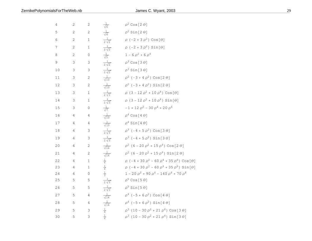
4 2 2 1è!!!!6 ρ2 Cos@2 θD5 2 2 1è!!!!6 ρ2 Sin@2 θD6 2 1 1
2 è!!!!2 ρ H−2 + 3 ρ2L Cos@θD7 2 1 1
2 è!!!!2 ρ H−2 + 3 ρ2L Sin@θD8 2 0 1è!!!!5 1 − 6 ρ2 + 6 ρ4
9 3 3 12 è!!!!2 ρ3 Cos@3 θD
10 3 3 12 è!!!!2 ρ3 Sin@3 θD
11 3 2 1è!!!!!!10ρ2 H−3 + 4 ρ2L Cos@2 θD
12 3 2 1è!!!!!!10ρ2 H−3 + 4 ρ2L Sin@2 θD
13 3 1 12 è!!!!3 ρ H3 − 12 ρ2 + 10 ρ4L Cos@θD
14 3 1 12 è!!!!3 ρ H3 − 12 ρ2 + 10 ρ4L Sin@θD
15 3 0 1è!!!!7 −1 + 12 ρ2 − 30 ρ4 + 20 ρ6
16 4 4 1è!!!!!!10ρ4 Cos@4 θD
17 4 4 1è!!!!!!10ρ4 Sin@4 θD
18 4 3 12 è!!!!3 ρ3 H−4 + 5 ρ2L Cos@3 θD
19 4 3 12 è!!!!3 ρ3 H−4 + 5 ρ2L Sin@3 θD
20 4 2 1è!!!!!!14ρ2 H6 − 20 ρ2 + 15 ρ4L Cos@2 θD
21 4 2 1è!!!!!!14ρ2 H6 − 20 ρ2 + 15 ρ4L Sin@2 θD
22 4 1 14 ρ H−4 + 30 ρ2 − 60 ρ4 + 35 ρ6L Cos@θD
23 4 1 14 ρ H−4 + 30 ρ2 − 60 ρ4 + 35 ρ6L Sin@θD
24 4 0 13 1 − 20 ρ2 + 90 ρ4 − 140 ρ6 + 70 ρ8
25 5 5 12 è!!!!3 ρ5 Cos@5 θD
26 5 5 12 è!!!!3 ρ5 Sin@5 θD
27 5 4 1è!!!!!!14ρ4 H−5 + 6 ρ2L Cos@4 θD
28 5 4 1è!!!!!!14ρ4 H−5 + 6 ρ2L Sin@4 θD
29 5 3 14 ρ3 H10 − 30 ρ2 + 21 ρ4L Cos@3 θD
30 5 3 14 ρ3 H10 − 30 ρ2 + 21 ρ4L Sin@3 θD
ZernikePolynomialsForTheWeb.nb James C. Wyant, 2003 29
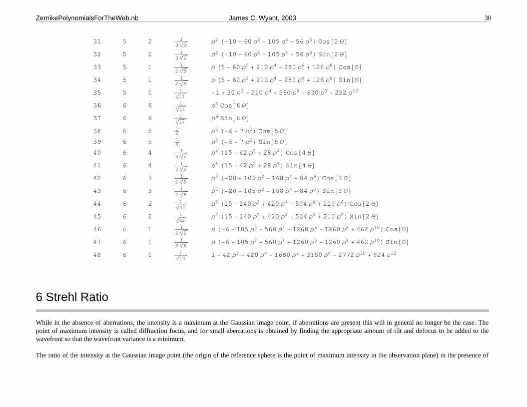
31 5 2 13 è!!!!2 ρ2 H−10 + 60 ρ2 − 105 ρ4 + 56 ρ6L Cos@2 θD
32 5 2 13 è!!!!2 ρ2 H−10 + 60 ρ2 − 105 ρ4 + 56 ρ6L Sin@2 θD
33 5 1 12 è!!!!5 ρ H5 − 60 ρ2 + 210 ρ4 − 280 ρ6 + 126 ρ8L Cos@θD
34 5 1 12 è!!!!5 ρ H5 − 60 ρ2 + 210 ρ4 − 280 ρ6 + 126 ρ8L Sin@θD
35 5 0 1è!!!!!!11−1 + 30 ρ2 − 210 ρ4 + 560 ρ6 − 630 ρ8 + 252 ρ10
36 6 6 1è!!!!!!14ρ6 Cos@6 θD
37 6 6 1è!!!!!!14ρ6 Sin@6 θD
38 6 5 14 ρ5 H−6 + 7 ρ2L Cos@5 θD
39 6 5 14 ρ5 H−6 + 7 ρ2L Sin@5 θD
40 6 4 13 è!!!!2 ρ4 H15 − 42 ρ2 + 28 ρ4L Cos@4 θD
41 6 4 13 è!!!!2 ρ4 H15 − 42 ρ2 + 28 ρ4L Sin@4 θD
42 6 3 12 è!!!!5 ρ3 H−20 + 105 ρ2 − 168 ρ4 + 84 ρ6L Cos@3 θD
43 6 3 12 è!!!!5 ρ3 H−20 + 105 ρ2 − 168 ρ4 + 84 ρ6L Sin@3 θD
44 6 2 1è!!!!!!22ρ2 H15 − 140 ρ2 + 420 ρ4 − 504 ρ6 + 210 ρ8L Cos@2 θD
45 6 2 1è!!!!!!22ρ2 H15 − 140 ρ2 + 420 ρ4 − 504 ρ6 + 210 ρ8L Sin@2 θD
46 6 1 12 è!!!!6 ρ H−6 + 105 ρ2 − 560 ρ4 + 1260 ρ6 − 1260 ρ8 + 462 ρ10L Cos@θD
47 6 1 12 è!!!!6 ρ H−6 + 105 ρ2 − 560 ρ4 + 1260 ρ6 − 1260 ρ8 + 462 ρ10L Sin@θD
48 6 0 1è!!!!!!131 − 42 ρ2 + 420 ρ4 − 1680 ρ6 + 3150 ρ8 − 2772 ρ10 + 924 ρ12
6 Strehl Ratio
While in the absence of aberrations, the intensity is a maximum at the Gaussian image point, if aberrations are present this will in general no longer be the case. Thepoint of maximum intensity is called diffraction focus, and for small aberrations is obtained by finding the appropriate amount of tilt and defocus to be added to thewavefront so that the wavefront variance is a minimum.
The ratio of the intensity at the Gaussian image point (the origin of the reference sphere is the point of maximum intensity in the observation plane) in the presence of
ZernikePolynomialsForTheWeb.nb James C. Wyant, 2003 30
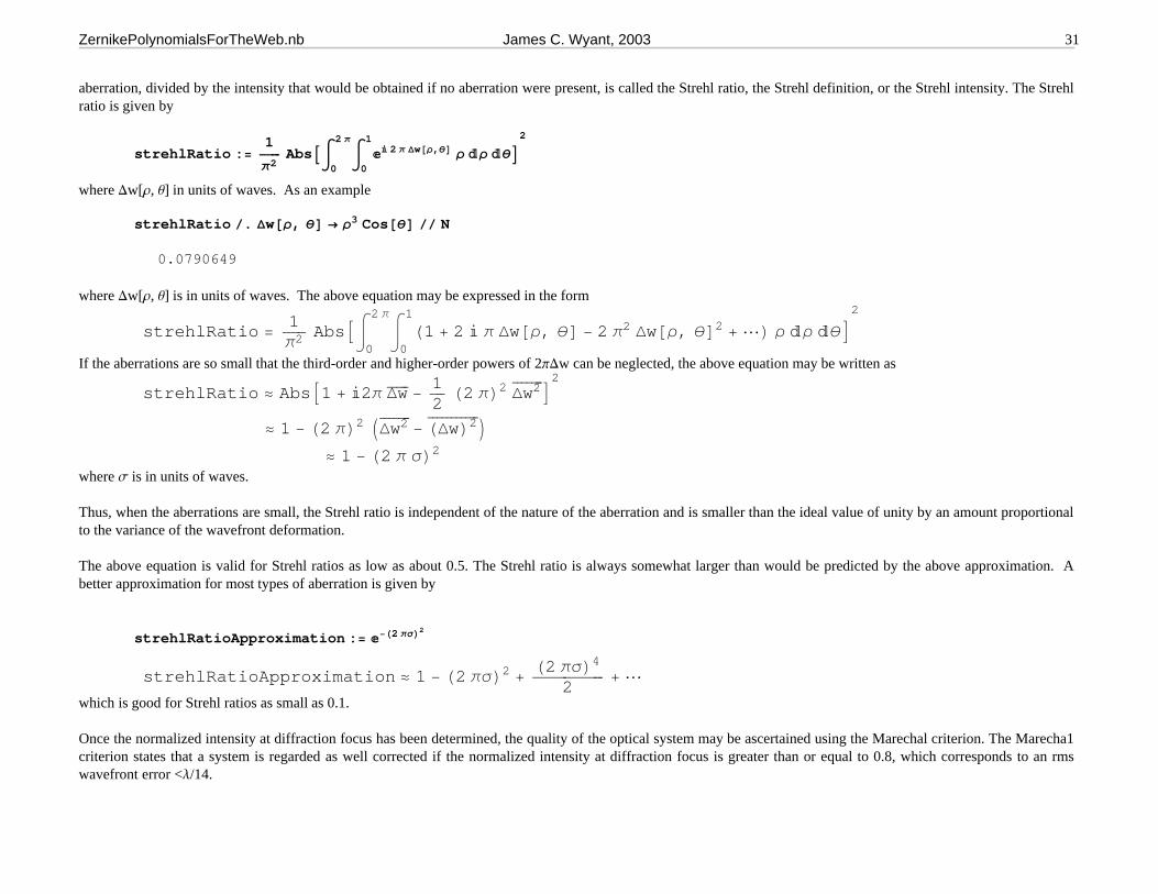
aberration, divided by the intensity that would be obtained if no aberration were present, is called the Strehl ratio, the Strehl definition, or the Strehl intensity. The Strehlratio is given by
strehlRatio :=1
π2 AbsA‡
0
2 π
‡0
12 π ∆w@ρ,θD ρ ρ θE
2
where Dw[r, q] in units of waves. As an example
strehlRatio ê. ∆w@ρ, θD → ρ3 Cos@θD êê N
0.0790649
where Dw[r, q] is in units of waves. The above equation may be expressed in the form
strehlRatio =1π2 AbsA‡
0
2 π
‡0
1
H1 + 2 π ∆w@ρ, θD − 2 π2 ∆w@ρ, θD2 + ∫L ρ ρ θE2
If the aberrations are so small that the third-order and higher-order powers of 2pDw can be neglected, the above equation may be written as
strehlRatio ≈ AbsA1 + 2π ∆w¯¯ −12
H2 πL2 ∆w2¯¯¯E2
≈ 1 − H2 πL2 I∆w2¯¯¯− H∆wL2¯¯¯¯¯ M
≈ 1 − H2 π σL2
where s is in units of waves.
Thus, when the aberrations are small, the Strehl ratio is independent of the nature of the aberration and is smaller than the ideal value of unity by an amount proportionalto the variance of the wavefront deformation.
The above equation is valid for Strehl ratios as low as about 0.5. The Strehl ratio is always somewhat larger than would be predicted by the above approximation. Abetter approximation for most types of aberration is given by
strehlRatioApproximation := −H2 πσL2
strehlRatioApproximation ≈ 1 − H2 πσL2 +H2 πσL4
2+ ∫
which is good for Strehl ratios as small as 0.1.
Once the normalized intensity at diffraction focus has been determined, the quality of the optical system may be ascertained using the Marechal criterion. The Marecha1criterion states that a system is regarded as well corrected if the normalized intensity at diffraction focus is greater than or equal to 0.8, which corresponds to an rmswavefront error <l/14.
ZernikePolynomialsForTheWeb.nb James C. Wyant, 2003 31

As mentioned above, a useful feature of Zernike polynomials is that each term of the Zernikes minimizes the rms wavefront error to the order of that term. That is, eachterm is structured such that adding other aberrations of lower orders can only increase the rms error. Removing the first-order Zernike terms of tilt and defocusrepresents a shift in the focal point that maximizes the intensity at that point. Likewise, higher order terms have built into them the appropriate amount of tilt and defocusto minimize the rms wavefront error to that order. For example, looking at Zernike term #9 shows that for each wave of third-order spherical aberration present, onewave of defocus should be subtracted to minimize the rms wavefront error and find diffraction focus.
7 References
Born, M. and Wolf, E., (1959). Principles of Optics, pp. 464-466, 767-772. Pergamon press, New York.Kim, C.-J. and Shannon, R.R. (1987). In "Applied Optics and Optical Engineering," Vol. X (R. Shannon and J. Wyant, eds.), pp. 193-221. Academic Press, New York.Wyant, J. C. and Creath, K. (1992). In "Applied Optics and Optical Engineering," Vol. XI (R. Shannon and J. Wyant, eds.), pp. 28-39. Academic Press, New York.Zernike, F. (1934), Physica 1, 689.
ZernikePolynomialsForTheWeb.nb James C. Wyant, 2003 32

8 Index
Introduction...1Calculating Zernikes...2Tables of Zernikes...3OSC Zernikes...6Zernike Plots...7Density Plots...73D Plots...8Cylindrical Plot 3D...10Surfaces of Revolution...143D Shadow Plots...15Animated Plots...16Animated Density Plots...16Animated 3D Shadow Plots...17Animated Cylindrical Plot 3D...18Two pictures stereograms...19Single picture stereograms...20Zernike polynomials and third-order aberrations...21Wavefront aberrations...21Zernike terms...21Table of Zernikes and aberrations...22Zernike Third-Order Aberration Table...23Seidel Aberration Table...25RMS Wavefront Aberration...27Strehl Ratio...30References...32Index...33
ZernikePolynomialsForTheWeb.nb James C. Wyant, 2003 33