university of groningen charge transport and … · charge transport and recombination in...
TRANSCRIPT
University of Groningen
Charge Transport and Recombination in Organic-Semiconductor DiodesWetzelaer, Gert-Jan
IMPORTANT NOTE: You are advised to consult the publisher's version (publisher's PDF) if you wish to cite fromit. Please check the document version below.
Document VersionPublisher's PDF, also known as Version of record
Publication date:2014
Link to publication in University of Groningen/UMCG research database
Citation for published version (APA):Wetzelaer, G-J. (2014). Charge Transport and Recombination in Organic-Semiconductor Diodes s.l.: s.n.
CopyrightOther than for strictly personal use, it is not permitted to download or to forward/distribute the text or part of it without the consent of theauthor(s) and/or copyright holder(s), unless the work is under an open content license (like Creative Commons).
Take-down policyIf you believe that this document breaches copyright please contact us providing details, and we will remove access to the work immediatelyand investigate your claim.
Downloaded from the University of Groningen/UMCG research database (Pure): http://www.rug.nl/research/portal. For technical reasons thenumber of authors shown on this cover page is limited to 10 maximum.
Download date: 29-05-2018

Charge Transport and Recombination in Organic-Semiconductor Diodes
Gert-Jan Wetzelaer
Charge Transport and Recombination in Organic-Semiconductor Diodes G.A.H. Wetzelaer PhD thesis University of Groningen Zernike Institute PhD thesis series 2014-05 ISSN: 1570-1530 ISBN: 978-90-367-6887-0 (Printed version)
978-90-367-6888-7 (Electronic version)
The research presented in this thesis was performed in the research group Molecular Electronics of the Zernike Institute for Advanced Materials at the University of Groningen, The Netherlands. This work forms part of the research program of the Dutch Polymer Institute (DPI), project #678. Cover design by Gert-Jan Wetzelaer with special thanks to Marianna Manca.
Charge Transport and Recombination in Organic-Semiconductor Diodes
Proefschrift
ter verkrijging van de graad van doctor aan de Rijksuniversiteit Groningen
op gezag van de rector magnificus prof. dr. E. Sterken
en volgens besluit van het College voor Promoties.
De openbare verdediging zal plaatsvinden op
vrijdag 28 maart 2014 om 11.00 uur
door
Gertjan Anton Hubert Wetzelaer
geboren op 29 april 1986 te Dwingeloo

Promotor Prof. dr. ir. P.W.M. Blom Beoordelingscommissie Prof. dr. C.J. Brabec Prof. dr. N.C. Greenham Prof. dr. D.M. de Leeuw


vi
| Contents
1. Introduction .......................................................................................................................... 1
1.1 Introduction ................................................................................................................................. 2
1.2 Conjugated polymers .................................................................................................................. 2
1.3 Charge transport in organic semiconductors .......................................................................... 3
1.4 Device operation of organic diodes .......................................................................................... 6
1.5 Device characteristics of organic diodes .................................................................................. 8
1.6 Device characteristics of organic solar cells .......................................................................... 13
1.7 Charge trapping in organic semiconductors ........................................................................ 15
1.8 Charge-carrier recombination in organic-semiconductor devices .................................... 17
1.9 Scope and outline of this thesis............................................................................................... 18
References ........................................................................................................................................ 21
2. Asymmetric electron and hole transport in a high-mobility n-type conjugated polymer ................................................................................................................................................. 25
2.1 Introduction .............................................................................................................................. 26
2.2 Electron Transport ................................................................................................................... 27
2.3 Hole transport ........................................................................................................................... 30
2.4 Temperature activation of electron and hole transport ...................................................... 32
2.5 Thin-film transistors ................................................................................................................ 33
2.6 Quantum-chemical calculations ............................................................................................. 34
2.7 Conclusions ............................................................................................................................... 39
Experimental Section ..................................................................................................................... 39
References ........................................................................................................................................ 41
3. Trap-assisted and Langevin-type recombination in organic light-emitting diodes........ 45
3.1 Introduction .............................................................................................................................. 46
3.2 Ideality factor of an OLED ...................................................................................................... 47
3.3 Luminance ideality factor ........................................................................................................ 49
vii
3.4 Conclusions ............................................................................................................................... 52
References ........................................................................................................................................ 54
4. Trap-assisted recombination rate in disordered organic semiconductors ...................... 57
4.1 Introduction .............................................................................................................................. 58
4.2 Determination of the capture coefficient .............................................................................. 60
4.3 Radiative trap-assisted recombination .................................................................................. 62
4.4 Predictive modeling ................................................................................................................. 63
4.5 Conclusions ............................................................................................................................... 64
References ........................................................................................................................................ 65
5. Validity of the Einstein relation in disordered organic semiconductors ......................... 67
5.1 Introduction .............................................................................................................................. 68
5.2 Ideality factor of single-carrier diodes ................................................................................... 69
5.3 Ideality factor of double-carrier diodes ................................................................................. 72
5.3 Conclusions ............................................................................................................................... 74
References ........................................................................................................................................ 75
6. Origin of the dark-current ideality factor in polymer:fullerene bulk-heterojunction solar cells ................................................................................................................................. 77
6.1 Introduction .............................................................................................................................. 78
6.2 Ideality factor of organic solar cells in dark and under illumination ................................ 79
6.3 Conclusions ............................................................................................................................... 83
References ........................................................................................................................................ 84
7. Quantifying bimolecular recombination in organic solar cells in steady state ............... 85
7.1 Introduction .............................................................................................................................. 86
7.2 Analytical expression for obtaining the Langevin prefactor............................................... 87
7.3 Application to bulk-heterojunction solar cells ..................................................................... 90
7.4 Conclusions ............................................................................................................................... 93
Experimental section ...................................................................................................................... 94
References ........................................................................................................................................ 95
8. Identifying the nature of charge recombination in organic solar cells from charge-transfer state electroluminescence ......................................................................................... 97
8.1 Introduction .............................................................................................................................. 98
viii
8.2 Ideality factor of the charge-transfer state electroluminescence ........................................ 98
8.3 Charge-transfer state electroluminescence efficiency ....................................................... 101
8.4 Trap-assisted recombination in P3HT:PCBM ................................................................... 104
8.5 Conclusions ............................................................................................................................. 105
Experimental section .................................................................................................................... 106
References ...................................................................................................................................... 107
Summary ............................................................................................................................... 111
Samenvatting ........................................................................................................................ 115
List of publications ............................................................................................................... 119
Acknowledgments ................................................................................................................ 123
1
Introduction This introductory chapter is devoted to the device physics of organic-semiconductor diodes. After introducing the basic concepts of organic semiconductors, their charge transport is treated, which differs substantially from
that in classical inorganic semiconductors. Next, a basic description of the operation and device characteristics of several types of organic-semiconductor devices is provided. Important subjects in this thesis are charge trapping and recombination, which are introduced subsequently. Finally, an overview of this thesis is given.
1. Introduction
1
Chapter 1. Introduction
2
1.1 Introduction Since the discovery of electrical conduction in organic materials in the 1950’s and 1960’s, the field of organic electronics gained more and more attention. Starting off with the observed photoconductivity and electroluminescence in organic crystals, such as naphthalene and anthracene [1-4], research on organic electronics went through a rapid development. This resulted in organic-semiconductor devices like organic light-emitting diodes (OLEDs) [5,6], organic photovoltaic cells (OPV) [7,8], and organic field-effect transistors (OFETs) [9], closing the gap to commercialization. The attraction towards organic electronics stems from its potential application as a low-cost replacement for conventional semiconductor and lighting technologies. In this respect, the so-called conjugated polymers form a striking class of organic semiconductors. Polymers are widely known for their application in insulating plastics, and hence their easy, flexible and low-cost processing properties. Conjugated polymers can therefore be seen as semiconducting plastics, opening a whole new world of potential applications. Conjugated polymers and small molecules can be made soluble in organic solvents, by modification of their chemical structure. Therefore, thin layers of organic semiconductor can be deposited from solution [10]. This can be achieved by various coating techniques, including inkjet printing, slot-die coating and spin coating. These low-temperature techniques offer the advantage of using flexible substrates. As a result, flexible thin-film electronic devices can be fabricated using a high-speed roll-to-roll process. This can yield large-area and lightweight lighting sources, displays, and solar cells. However, despite the abundance in future potential, there are still some issues that have to be solved for organic-semiconductor devices to compete with present-day technology. Most importantly, power-conversion efficiencies and lifetime have to be increased, which applies to both OLED and OPV technologies. In order to improve the performance of these organic diodes, a fundamental understanding of the loss mechanisms is indispensable. 1.2 Conjugated polymers Conjugated polymers are polymers that comprise a carbon backbone with alternatingly single and double bonds. Normally, polymers are made up of σ-bonds between the constituent carbon atoms and exhibit insulating properties. In conjugated polymers however, the alternating single and double bonds cause each carbon atom to form only three bonds with its
Figure 1.1. Chemical structure of polyacetylene, comprising alternating single and double bonds between the carbon atoms.
1.3 Charge transport in organic semiconductors
3
adjacent atoms, giving rise to the presence of an unbound electron in a pz orbital for each carbon atom. These pz orbitals, due to their mutual overlap, participate in the formation of π bonds along the conjugated carbon backbone, thereby delocalizing the π electrons along the entire conjugation path. A π band is formed and the delocalized π electrons can jump from site to site between adjacent carbon atoms. The filled π band is referred to as the highest occupied molecular orbital (HOMO) and the empty π* band is referred to as the lowest unoccupied molecular orbital (LUMO). Such a conjugated system has semiconducting properties, where the HOMO and LUMO are equivalent to the valence band and conduction band known from classical semiconductor physics. There is a forbidden energy gap between the HOMO and the LUMO, typically ranging from ~1 to ~4 eV for these materials. The origin of this gap stems from the bond-length alternation along the carbon backbone and the size of the conjugated system [11]. Typical energy gaps of organic semiconductors allow them to interact with light in the visible spectrum. Upon excitation with light, an electron can be promoted from HOMO to LUMO, leaving a hole behind. Also the reverse process can take place, where an excited electron recombines with a hole, resulting in the emission of a photon. Because of these optical properties and the possibility of charge transport along the conjugation path, organic semiconductors comprise the necessary requirements for use in optoelectronic devices. 1.3 Charge transport in organic semiconductors Charge transport in organic semiconductors, however, has vastly distinct properties as compared to classical, inorganic semiconductors. In a conjugated polymer, the conjugation along the backbone can be disturbed due to twisted and kinked chains, as well as chemical defects. The energetic position of the HOMO and LUMO depends on the size of the conjugated system [11]. Because of the disordered configuration of conjugated polymers and molecules, organic semiconductors are therefore typically subject to energetic disorder. This has important implications for the charge transport. Due to the absence of a three-dimensional periodic lattice structure, the concept of band conduction does not apply and standard semiconductor models are not suitable to describe charge transport in an organic semiconductor. In an ordered inorganic semiconductor, the carrier mean free path is large. In an organic semiconductor, however, the carrier mean free path is limited because of the presence of localized states that are distributed in energy. In order to participate in charge transport, charge carriers must hop from one state to another. A hop upward in energy requires the absorption of a phonon, while a downward hop releases a phonon. This phonon-assisted hopping was proposed by Conwell [12] and Mott [13,14] to describe impurity conduction in inorganic semiconductors. A description for the transition rates between hopping sites was given by Miller and Abrahams [15]. In a semiconductor, charge transport is typically characterized in terms of the charge-carrier mobility. The charge-carrier mobility characterizes the drift velocity of a charge carrier
Chapter 1. Introduction
4
under application of an electric field. In order to characterize charge transport in organic semiconductors, a description of the mobility is essential. Due to the hopping nature of transport, mobilities in organic semiconductors are generally much lower than in inorganic semiconductors. In addition, the dependence of the mobility on temperature and electric field also exhibits different behavior. A theoretical description of the charge-carrier mobility in disordered organic semiconductors was first provided by Bässler in 1993 [16]. In this seminal work, an expression for the mobility in the case of Miller-Abrahams hopping in a Gaussian density-of-states distribution was proposed. Since such a system cannot be solved analytically, Monte Carlo simulations were carried out. On the basis of the Monte Carlo simulations, the charge-carrier mobility μ was found to be temperature and field dependent, and in the limit of high electric fields is given by [16]
( )[ ]( )( )[ ]( )
<−
≥−×
−= ∞ 5.1Σ;25.2/exp
5.1Σ;Σ/exp32exp
2
222
EkTσC
EkTσCkTσμμ (1.1)
where μ∞ is the mobility in the limit T → ∞, σ is the variance of the Gaussian density-of-states distribution, k is the Boltzmann constant, T is the temperature, C is a constant that depends on the site spacing, which is typically 1-2 nm in organic semiconductors, Σ is the degree of positional disorder, and E is the electric field. From this mobility description of hopping transport in a Gaussian density-of-states distribution, some important features can be recognized. In contrast to the case of band conductors, where transport is limited by phonon scattering, Eq. (1.1) predicts a decreasing mobility with decreasing temperature, where ln(μ) scales with 1/T2. The origin for this is that hopping transport is phonon assisted, which implies that it is temperature activated. Furthermore, the hopping process is also activated by the electric field, resulting in a field dependence of the mobility [16]. Later, it was discovered that the mobility in disordered organic semiconductors is influenced by another factor, which is the charge-carrier density. In 1998, Vissenberg and Matters [17] introduced a mobility model for organic field-effect transistors, based on variable-range hopping in an exponential density-of-states distribution. In a field-effect transistor, application of a gate voltage results in the accumulation of charges in the channel. In case of an energetically-distributed density of states, the carriers induced by the gate voltage first fill the lower-lying states. As the carrier density increases, more hopping states become available, resulting in less energy required for a charge carrier to jump to a neighboring site [17]. In a field-effect transistor, only a moderate electric field between source and drain is present, since the channel length is typically in the order of micrometers. In an organic thin-film diode, however, the electrode separation equals the film thickness, which is generally around 100 nm. Therefore, the electric field in an organic diode is considerably higher. This also implies that the influence of the electric field on the charge-carrier mobility is important
1.3 Charge transport in organic semiconductors
5
in diodes. However, even though a diode does not have a gate electrode that induces charges, also the charge-carrier density plays an important role. By applying a voltage, carriers are injected into the organic-semiconductor layer. As a result, applying an electric field is also accompanied by in the buildup of charge density. This makes it difficult to separate the influence electric field and charge concentration on the charge-carrier mobility. In 2003, Tanase et al. [18] reported a unification of the charge-carrier mobility in organic diodes and field-effect transistors. It was shown that the large difference in mobility between these devices could be explained by the difference in charge concentration, being much higher in a field-effect transistor due to application of a gate voltage. Furthermore, it was demonstrated that, at room temperature, the enhancement of the mobility at higher fields in a diode is mainly due to the increased carrier density, rather than the electric field itself [19]. However, at lower temperatures, the field dependence of the mobility becomes dominant. Since both density and field effects are important in describing the charge-carrier mobility of disordered organic semiconductors, a description that incorporates both these effects – together with the temperature dependence – is essential. Such a full description of the mobility was obtained by Pasveer et al. [20] from a numerical solution of the master equation for hopping transport in a Gaussian density-of-states distribution. The numerical data were described by the following parametrization scheme, ),(),(),,( ETfnTμEnTμ nn ≈ , (1.2) [ ]δ
n naσσTμnTμ )2)(ˆˆ(exp)(),( 3221
0 −= , (1.3) [ ]2
0ˆexp)( σCμTμ −= ∞ , (1.4)
( )2
2
ˆ4lnln)ˆˆln(2
σσσδ −−≡ , (1.5)
( )
−
+−= 18.012.2ˆ44.0exp),(
22/3
σEqaσETf , (1.6)
with )(0 Tμ the mobility in the limit of zero charge carrier density and electric field, and C = 0.42, a the hopping distance, q the elementary charge, and n the charge-carrier density. The normalized Gaussian variance is defined as kTσσ /ˆ ≡ .
The mobility model by Pasveer et al. [20] provides a good description of charge transport in organic diodes, including the effect of carrier concentration. One of the implications of this model is that also the temperature dependence of the mobility is affected by the presence of a carrier density. In the limit of vanishing charge-carrier density, the temperature dependence of Eq. (1.1) is recovered, where ln(μ) scales with 1/T2 [20]. However, for typical charge concentrations present in organic diodes [21], in the order of 1021 m-3, the
Chapter 1. Introduction
6
temperature dependence modifies to an Arrhenius Tμ /1)ln( ∝ behavior [22,23]. Experimentally, a universal relation was found between the mobility and its temperature activation in organic diodes [24]. Using the empirical description for the Arrhenius temperature dependence of the zero-field mobility
−= ∞ kT
μTμ Δexp)( , (1.7)
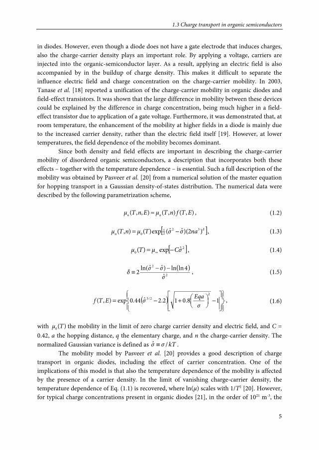
with Δ the activation energy, a universal value for the mobility μ∞ of 30-40 cm2/Vs at infinite temperature was found [24]. A consequence of this finding is that the temperature dependence of the mobility can be predicted from its room-temperature value. From the theoretical models by Bässler [16] and Pasveer et al. [20] it follows that the width of the density-of-states distribution is the key determinant of the temperature dependence of the mobility. A higher activation energy thus implies more energetic disorder. The universal relation between the mobility and its temperature activation [24] therefore shows that energetic disorder plays an important role in the value of the charge-carrier mobility. 1.4 Device operation of organic diodes Organic semiconductors have become immensely popular since it was discovered that they could be successfully applied in optoelectronic devices, such as light-emitting diodes [5,6] and solar cells [7,8]. The simplest form of such an organic diode comprises a thin layer of organic semiconductor sandwiched between two metallic electrodes, of which one typically is transparent to permit the transmission of light. In an OLED, light is generated inside the
Figure 1.2. Schematic energy-band diagram of a single-layer organic light-emitting diode. Electrons and holes are represented by full and empty circles, respectively. The first process is charge injection from the electrodes, which is followed by transport through the active layer. Subsequently, an exciton is formed, which decays under emission of a photon. The last two steps form the recombination process.
LUMO
HOMO
Anode
Cathode
hν
1.4 Device operation of organic diodes
7
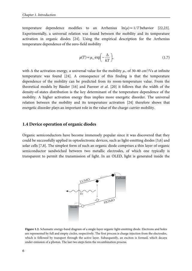
organic-semiconductor layer upon applying a voltage. The first step in this process is the injection of charge carriers from the electrodes into the organic-semiconductor layer. Efficient charge injection can be achieved when the work function of the anode and cathode match the HOMO and LUMO of the organic semiconductor, respectively, to obtain Ohmic hole and electron contacts. This implies that there is a difference in work function between anode and cathode, which gives rise to a built-in voltage. When a voltage larger than the built-in voltage is applied, holes and electrons are injected from the anode and cathode, respectively. Assisted by the electric field imposed by the applied voltage, electrons and holes are transported toward each other across the active layer. When an electron and a hole meet, they can form an exciton and recombine. The decay of an exciton can either proceed radiatively, thus by emission of a photon, or nonradiatively. The energy, and hence wavelength, of the emitted photon is determined by the forbidden energy gap between HOMO and LUMO. The photon is then transmitted through the transparent electrode, completing the conversion of electrical energy into light. In an organic solar cell, or organic photovoltaic diode, the reverse process takes place. In such a device, sunlight is converted into electricity. The basic device layout is the same as in an OLED. An incoming photon is transmitted through the transparent electrode into the organic layer. The photon is absorbed by the organic semiconductor, upon which an electron is promoted from the HOMO to the LUMO, leaving a hole behind in the HOMO. As a result, an exciton is created that has to be split up into free charge carriers. However, organic semiconductors typically have low relative dielectric constants of 2-4, which results in a high exciton binding energy [25], making it difficult to dissociate the exciton. To facilitate exciton dissociation, an organic solar cell usually consists of an organic heterojunction. In such a heterojunction, an electron donor and acceptor are brought together [7]. The donor and acceptor are chosen such that electron transfer from donor to acceptor – or hole transfer from acceptor to donor – is energetically favorable. As a result, exciton dissociation can take place
Figure 1.3. Schematic energy-band diagram of a bulk-heterojunction organic solar cell. The solid lines represent the energy levels of the donor, while the dashed lines represent the energy levels of the acceptor. A photon is first absorbed by the donor material under formation of an exciton. After diffusing to a donor-acceptor interface, the exciton dissociates, upon which electrons and holes are transported through the LUMO of the acceptor and the HOMO of the donor, respectively. Finally, the photogenerated charges are extracted by the electrodes.
LUMO
HOMO
Anode
Cathodehν
Chapter 1. Introduction
8
at the donor-acceptor interface. However, an exciton can only arrive at this interface when the interface is within the exciton diffusion length, which is typically 1-10 nm in organic semiconductors [26-30]. In other words, only excitons created in close proximity to the donor-acceptor interface can be dissociated and converted into free charge carriers, while the other excitons decay back to the ground state. This problem has been overcome by using a so-called bulk heterojunction [8]. In a bulk heterojunction, the donor and acceptor materials are intimately mixed and form an interpenetrating phase-separated network, in which dimensions of the donor and acceptor phases are in the order of the exciton diffusion length. Therefore, in the proximity of every generated exciton there is an interface with an acceptor where fast dissociation takes place. Hence, charge generation takes place everywhere in the active layer [31]. After exciton dissociation, the electron-hole pair may still be Coulombically bound in a charge-transfer state. Once the charge-transfer excitons are separated into free charge carriers, the charges are transported to the electrodes. This process is assisted by the built-in electric field, induced by the built-in voltage due the difference in work function between the electrodes. Holes and electrons are the collected by the anode and cathode, respectively, and driven into the external circuit, producing an electrical current. 1.5 Device characteristics of organic diodes In both OLEDs and organic solar cells, one of the most important processes is the transport of charge-carriers. A relatively simple technique to examine the transport of electrons or holes through organic-semiconductor layers is by fabricating electron-only or hole-only devices. Such test devices consist of one injecting electrode, which ensures Ohmic charge injection, while the counterelectrode blocks the injection of carriers of the opposite sign. In a hole-only device, for instance, a high work function anode is used for Ohmic hole injection into the HOMO, while the work function of the cathode is sufficiently high to impose a large-enough injection barrier for electron injection into the LUMO. As a result, the current in such a device will be a pure hole current, since electrons are practically not injected into the organic semiconductor. An electron-only device can be constructed in a similar manner. Conjugated polymers and small molecules, as typically used in organic light-emitting diodes or solar cells are undoped semiconductors. When these semiconductors are sandwiched between two electrodes, a metal-insulator-metal (MIM) diode stack is formed. Single-carrier organic diodes frequently consist of an Ohmic injecting contact and a non-Ohmic collection contact. In general, when electrodes with different work functions are used, an internal electric field will build up resulting from a built-in voltage Vbi across the undoped semiconductor, which equals the difference in work function of the electrodes. This built-in voltage gives rise to the rectifying properties of organic diodes. In order to understand the device characteristics of organic diodes, we will now give a derivation for their current-voltage behavior, which can be used to study the charge transport in organic materials.
1.5 Device characteristics of organic diodes
9
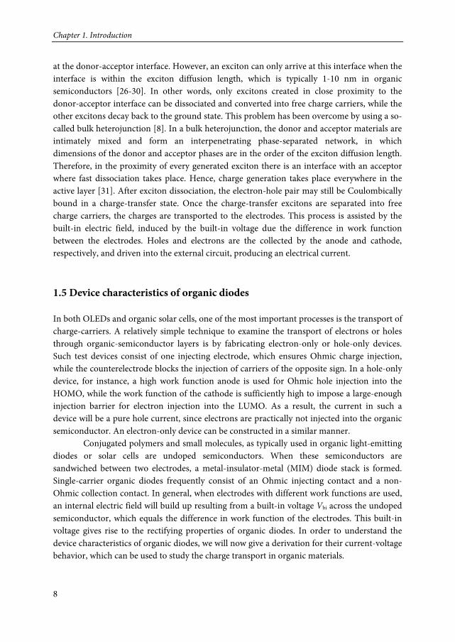
As a reference, we consider the case of a hole-only MIM diode with one Ohmic and one non-Ohmic contact, as shown in Fig. 1.4(a). The collecting contact at x = L, where x denotes the position within the diode and L is the film thickness, is separated from the valence band by a barrier height, φb. The injecting contact at x = 0 aligns with the valence band. For both contacts the energy barrier to the conduction band is so large that electron injection can be neglected. The built-in voltage Vbi is then equal to the barrier height φb.
At high positive bias on the Ohmic contact, larger than the built-in voltage, the resulting electric field becomes positive, pointing towards the collecting contact. Holes are injected and the current is dominated by drift. The current becomes limited by the uncompensated charges of the injected holes, leading to a space-charge-limited current (SCLC) that can be analytically described by the Mott-Gurney equation [32] as
3
2bi )(
89
LVV
εμJ−
= , (1.8)
with J the current density, ε the dielectric constant, μ the charge-carrier mobility, and V the applied voltage. Using this analytical equation, the charge-carrier mobility can be directly obtained from current density versus voltage (J-V) measurements on single-carrier devices [33].
So the drift current in an organic diode is a space-charge-limited current. Below the built-in voltage, however, the current will be dominated by diffusion of charge carriers. As shown in Fig. 1.4(a), we now apply a small positive bias on the injecting contact. When the bias is smaller than the built-in voltage the electric field is still negative, pointing towards the injecting contact. The drift current due to the injected holes is therefore negative. However, the gradient in the hole density leads to diffusion of holes towards the collecting contact. The net positive current then results from the positive diffusion current that dominates over the negative drift current.
Figure 1.4. Energy-band diagram of an organic hole-only MIM diode. The layer thickness is L and x denotes the position in the diode. The contact at x = 0 is Ohmic, while the collecting contact at x = L is separated from the valence band by a barrier height φb. (left) Thermal equilibrium and upon applying a small positive bias smaller than the built-in voltage (dashed). (right) Band diagram at thermal equilibrium when including band bending due to injected holes at the Ohmic contact.
EFE F
Diffusion
HOMO
LUMO
ϕbVbi
Driftx = 0 x = L
VEFE F
Diffusion
HOMO
LUMO
ϕbVbi
Driftx = 0 x = L
b
Chapter 1. Introduction
10
We will now derive an expression for this diffusion current, based on the classical Schottky diffusion theory. The original diffusion theory by Schottky [34] describes the situation for a metal contact on a doped semiconductor. In such a Schottky diode, majority carriers diffuse from the semiconductor into the metal to equilibrate the Fermi level. The charge of the remaining uncompensated dopants then leads to the build-up of an electric field in the depletion region, resulting in band bending. A similar model was used by Shockley for the current across a p-n junction, viz. a depletion region formed between a p- and n-doped semiconductor [35]. An alternative theory to describe the current in a Schottky diode, based on thermionic emission, is valid only for high charge-carrier mobilities [36,37], whereas diffusion is the limiting case in low-mobility semiconductors, like organic semiconductors.
In MIM structures, band bending due to uncompensated dopants is absent. Below, the appropriate boundary conditions [38] are introduced. We start with the hole-only MIM diode of Fig. 1.4(a). Following the classical derivation of Schottky for diffusion currents, the hole current density is given by
−=
dxdp
dxdE
kTpkTμJ v
pp , (1.9)
where the diffusion coefficient has been replaced by the hole mobility μp through the Einstein relation [39,40]. However, in contrast to a Schottky diode, the limit for integration in the MIM structure has to be set to the total device thickness L, since the device is fully depleted, leading to
L
vp
Lv
p kTxExkTpμdx
kTxEJ
00
)(exp)()(exp
−−=
− , (1.10)
with p the hole density and Ev the valence-band edge, or, analogously in this case the HOMO of the organic semiconductor. To evaluate this expression, we need to introduce the MIM boundary conditions for the charge carrier density p(x) and the valence band Ev(x) at the electrode-semiconductor interfaces x = 0 and x = L.
As shown in Fig. 1.4(a), the built-in voltage Vbi for this device is equal to φb, In that particular case the boundary conditions for the charge-carrier density at the electrodes of a metal-insulator-metal device are given by [38] vNp =)0( , (1.11a)
−=
kTφq
NLp bv exp)( , (1.11b)
whereas the boundary conditions for the valence band, with respect to the Fermi level of the hole-extraction contact, for V < Vbi are given by
1.5 Device characteristics of organic diodes
11
qVEv −=)0( , (1.12a) bv φqLE −=)( . (1.12b) Note that in this case a positive forward bias V at x = 0 lowers the internal voltage to φb - V, leading to a reduction of the negative drift current of holes towards the injecting contact at x = 0, which results in an enhanced positive current in the x-direction. Combination with Eq. (1.10) gives for the current
−
−
=
Lv
pvp dxkT
xEkTqVkTμNJ
0
)(exp1exp . (1.13)
Due to the absence of space charge there is no band bending in the MIM structure, so the positional dependence of the valence band Ev(x) is just a simple triangular shape, given by
−
+−=L
xVφVqxE b
v
)()( , (1.14)
yielding
−
−=
− kT
qVkTφq
VφqLkTdx
kTxE b
b
Lv expexp
)()(exp
0
. (1.15)
Substituting Eq. (1.15) into Eq. (1.13) then leads to an analytical current-density expression for the diffusion-limited current in a MIM diode, given by
−
−
−
=
kTqV
kTφq
L
kTqVVφNμq
Jb
bvp
p
expexp
1exp)(. (1.16)
A similar expression was obtained by Paasch et al. [41]. We note that the use of a constant mobility in our derivation is valid since in the diffusion regime the carrier densities in the diode are sufficiently low such that mobility enhancement due to DOS filling [17] does not play a role [20]. Before comparing Eq. (1.16) to experimental data, it is essential to consider that for Ohmic contacts on insulators or undoped semiconductors charge carriers diffuse from the electrode into the semiconductor, forming an accumulation region close to the contact [21]. As shown in Fig. 1.4(b), the accumulated charge carriers close to the injecting contact at x = 0 cause band bending and reduce the built-in voltage of the device. Reported
Chapter 1. Introduction
12
values for this band bending, here described by the parameter b, typically lie in the range of 0.2-0.3 V and depend also on energetic disorder [42-46]. To account for this accumulation, we approximate the energy band diagram of the MIM diode by the dashed lines in Fig. 1.4(b). In this way, the reduction of the built-in voltage is taken into account, while maintaining the triangular potential. The boundary conditions are then modified to
−=
kTqbNp v exp)0( , (1.17a)
−=
kTφq
NLp bv exp)( , (1.17b)
)()0( bVqEv +−= , (1.17c) bv φqLE −=)( . (1.17d) The current equation, Eq. (1.16), is for this case modified to
−
−
−
−−
=
kTqV
kTbφq
kTqbL
kTqVVbφNμq
Jb
bvp
p
exp)(
expexp
1exp)(. (1.18)
Clearly, the band-bending parameter b does not only reduce the built-in voltage, but also has a large impact on the current close to the Vbi and above Vbi. Therefore, we introduce the band-bending parameter b according to
−
= 2
2ln
22
εkTLNq
qkTb v , (1.19)
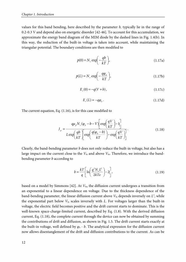
based on a model by Simmons [42]. At Vbi, the diffusion current undergoes a transition from an exponential to a linear dependence on voltage. Due to the thickness dependence of the band-bending parameter, the linear diffusion current above Vbi depends inversely on L3, while the exponential part below Vbi scales inversely with L. For voltages larger than the built-in voltage, the electric field becomes positive and the drift current starts to dominate. This is the well-known space-charge-limited current, described by Eq. (1.8). With the derived diffusion current, Eq. (1.18), the complete current through the device can now be obtained by summing the contributions of drift and diffusion, as shown in Fig. 1.5. The drift current starts exactly at the built-in voltage, well defined by φb - b. The analytical expression for the diffusion current now allows disentanglement of the drift and diffusion contributions to the current. As can be
1.6 Device characteristics of organic solar cells
13
seen in Fig. 1.5, the analytical description reproduces the result of a numerical drift-diffusion model [38], which is based on solving the Poisson and current-continuity equations. The simple analytical model can be used to describe the current-voltage behavior of single-carrier diodes, which directly yields the injection barrier and charge-carrier mobility. In double-carrier devices, such as OLEDs and solar cells, the built-in voltage is maximized – in the ideal case – due to the presence of an Ohmic hole and electron contact. Qualitatively, the current-voltage characteristics will appear similar to the single-carrier diode in Fig. 1.5. However, in a double-carrier device, the effects of charge recombination have to be taken into account. This can be done numerically with the aforementioned drift-diffusion model [38]. A large part of this thesis is devoted to the investigation of diffusion-driven currents in single-carrier diodes, OLEDs, and bulk-heterojunction solar cells. It is demonstrated that charge trapping and recombination play an important role in the behavior of these diffusion currents. 1.6 Device characteristics of organic solar cells The current-voltage characteristics of an organic solar cell in dark and an OLED are very similar. In principle, a bulk-heterojunction solar cell can be described with an effective medium approach, where the donor-acceptor blend is treated as one semiconductor [38]. The electron transport takes place through the LUMO of the acceptor, while the hole transport takes place through the HOMO of the donor. Assuming Ohmic electron and hole contacts, the built-in potential is then determined by the energetic difference between the HOMO of the donor and the LUMO of the acceptor.
Figure 1.5. Current density-voltage characteristics for a device with φb = 0.7 V, μp = 1×10⁻⁹ m2/Vs, Nv = 3×1026 m-3, L = 100 nm, T = 295 K, and ε = 3ε0. The dotted and solid lines are the analytically calculated characteristics for diffusion, drift, and the sum of drift and diffusion. The dashed line represents a numerical simulation [38] with the exactly the same parameters.
Chapter 1. Introduction
14
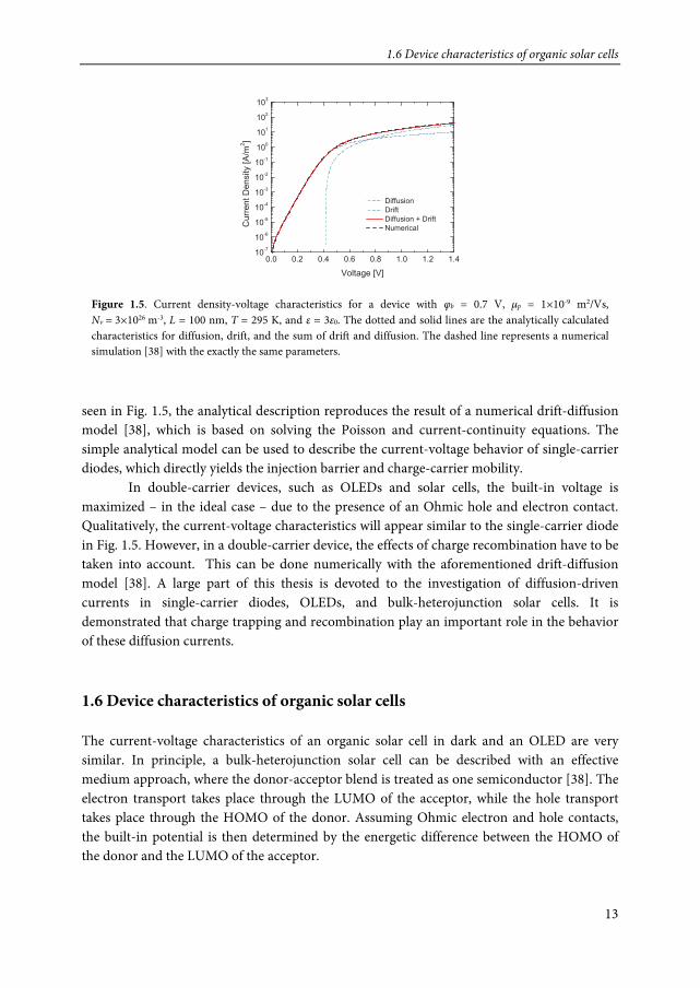
Under illumination, the solar cell produces a photocurrent. A typical current-voltage characteristic of an organic bulk-heterojunction solar cell is displayed in Fig. 1.6. In the fourth quadrant, the solar cell exhibits a negative current at a positive voltage and is therefore delivering power. At 0 V, the device is under short-circuit conditions and the electric field in the active layer equals the built-in field. Once separated, photogenerated charge carriers are driven by this field toward the electrodes. The resulting current density is the short-circuit current density Jsc. When the bias is increased, the electric field decreases. This typically results in a smaller photocurrent, which is caused by charge-carrier recombination prior to charge extraction at the electrodes. The current is zero at the open-circuit voltage Voc. At this voltage, all photogenerated charge carriers recombine. This implies that the open-circuit voltage is limited by the amount of recombination that is present in the device. Therefore, a reduction in the recombination strength would lead to a higher open-circuit voltage. The open-circuit voltage is lower than the built-in voltage and can be expressed as [47]
−=GNk
qkT
qE
V R2cvgap
oc ln , (1.20)
with Egap the energy gap between the HOMO of the acceptor and the LUMO of the donor, kR the bimolecular recombination coefficient, Ncv the density of states, and G the generation rate of excitons. Since there exists a balance between generation and recombination of charge carriers at the open-circuit voltage, studying the dependence of Voc on the illumination intensity, which is proportional to the generation rate G, can provide valuable information on charge recombination in the solar cell. Moving from short circuit to open circuit along the J-V characteristics, we are passing the region that determines the fill factor (FF). The fill factor is defined as the ratio between the maximum-power point and the product of Jsc and Voc. The maximum-power point is the point where the product of the current density and voltage has its maximum value. Also the fill
Figure 1.6. Typical current density-voltage characteristic of an organic bulk-heterojunction solar cell. The characterization parameters Jsc, Voc, and FF are indicated. The maximum-power point (MPP) is also shown, where the maximum power output that the solar cell can supply is represented by the filled rectangle.
Voc
JscMPP
FF = _____
1.7 Charge trapping in organic semiconductors
15
factor is strongly affected by charge recombination [48]. The power-conversion efficiency of the solar cell can be expressed as
I
VJχ FFocsc= , (1.21)
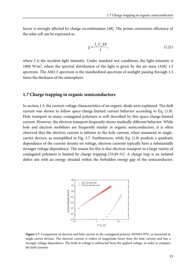
where I is the incident light intensity. Under standard test conditions, the light intensity is 1000 W/m2, where the spectral distribution of the light is given by the air mass (AM) 1.5 spectrum. The AM1.5 spectrum is the standardized spectrum of sunlight passing through 1.5 times the thickness of the atmosphere. 1.7 Charge trapping in organic semiconductors In section 1.5, the current-voltage characteristics of an organic diode were explained. The drift current was shown to follow space-charge-limited current behavior according to Eq. (1.8). Hole transport in many conjugated polymers is well described by this space-charge-limited current. However, the electron transport frequently shows markedly different behavior. While hole and electron mobilities are frequently similar in organic semiconductors, it is often observed that the electron current is inferior to the hole current, when measured in single-carrier devices, as exemplified in Fig. 1.7. Furthermore, while Eq. (1.8) predicts a quadratic dependence of the current density on voltage, electron currents typically have a substantially stronger voltage dependence. The reason for this is that electron transport in a large variety of conjugated polymers is limited by charge trapping [33,49-51]. A charge trap is an isolated defect site with an energy situated within the forbidden energy gap of the semiconductor.
Figure 1.7. Comparison of electron and hole current in the conjugated polymer MDMO-PPV, as measured in single-carrier devices. The electron current is orders of magnitude lower than the hole current and has a stronger voltage dependence. The built-in voltage is subtracted from the applied voltage, in order to compare the drift currents.
Chapter 1. Introduction
16
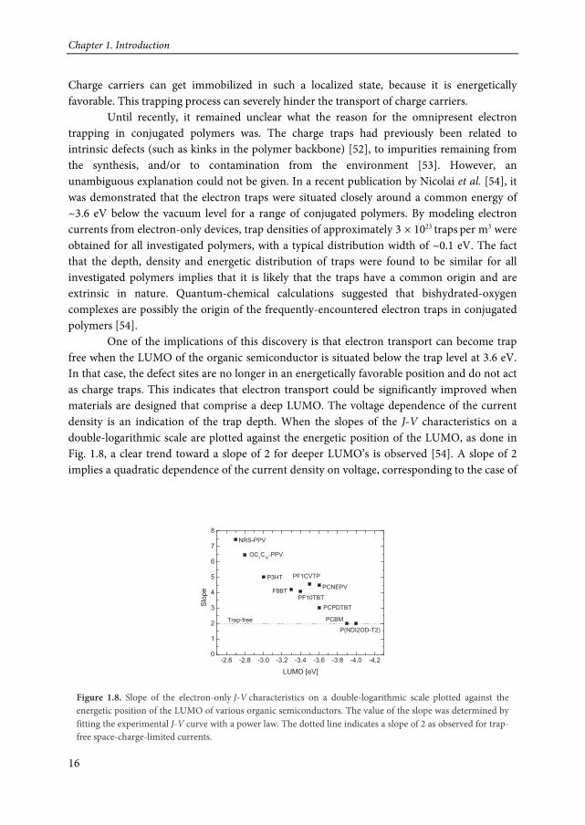
Charge carriers can get immobilized in such a localized state, because it is energetically favorable. This trapping process can severely hinder the transport of charge carriers. Until recently, it remained unclear what the reason for the omnipresent electron trapping in conjugated polymers was. The charge traps had previously been related to intrinsic defects (such as kinks in the polymer backbone) [52], to impurities remaining from the synthesis, and/or to contamination from the environment [53]. However, an unambiguous explanation could not be given. In a recent publication by Nicolai et al. [54], it was demonstrated that the electron traps were situated closely around a common energy of ~3.6 eV below the vacuum level for a range of conjugated polymers. By modeling electron currents from electron-only devices, trap densities of approximately 3 × 10²³ traps per m3 were obtained for all investigated polymers, with a typical distribution width of ~0.1 eV. The fact that the depth, density and energetic distribution of traps were found to be similar for all investigated polymers implies that it is likely that the traps have a common origin and are extrinsic in nature. Quantum-chemical calculations suggested that bishydrated-oxygen complexes are possibly the origin of the frequently-encountered electron traps in conjugated polymers [54]. One of the implications of this discovery is that electron transport can become trap free when the LUMO of the organic semiconductor is situated below the trap level at 3.6 eV. In that case, the defect sites are no longer in an energetically favorable position and do not act as charge traps. This indicates that electron transport could be significantly improved when materials are designed that comprise a deep LUMO. The voltage dependence of the current density is an indication of the trap depth. When the slopes of the J-V characteristics on a double-logarithmic scale are plotted against the energetic position of the LUMO, as done in Fig. 1.8, a clear trend toward a slope of 2 for deeper LUMO’s is observed [54]. A slope of 2 implies a quadratic dependence of the current density on voltage, corresponding to the case of
Figure 1.8. Slope of the electron-only J-V characteristics on a double-logarithmic scale plotted against the energetic position of the LUMO of various organic semiconductors. The value of the slope was determined by fitting the experimental J-V curve with a power law. The dotted line indicates a slope of 2 as observed for trap-free space-charge-limited currents.
1.8 Charge-carrier recombination in organic-semiconductor devices
17
a trap-free space-charge-limited limit, as described by Eq. (1.8). 1.8 Charge-carrier recombination in organic-semiconductor devices In both OLEDs and organic solar cells, charge-carrier recombination is an important process. In an OLED, emission of photons is a direct result of charge recombination. In the ideal case, all injected electrons and holes recombine. In an organic solar cell, however, charge-carrier recombination is a loss process. To produce a photocurrent, photogenerated electrons and holes need to be extracted at the contacts. During their transport across the organic layer toward the contacts, electrons and holes can meet and recombine. As a result, they can no longer contribute to the photocurrent. Although the device layout of single-layer OLEDs and organic solar cells is very similar, these devices have very different requirements in terms of charge recombination in order to function efficiently. This paradox can be partially resolved by considering the expression for the bimolecular recombination rate )( 2
iR nnpkR −= , (1.22) with kR the bimolecular recombination coefficient, n and p the electron and hole concentrations, respectively, and ni the intrinsic carrier concentration of electrons and holes given by ni
2 = Ncv exp[-Egap/kT]. The term bimolecular recombination implies that the recombination rate is proportional to the product of the electron and hole concentrations. In an OLED, the current is produced by charge carriers injected from the electrodes. The charge concentration is then given by maximum electrostatically-allowed carrier density, i.e., the space-charge limit [33,55]. As a result, charge-carrier recombination is maximized. In a solar cell, however, the current is produced by photogenerated charges. The solar cell operates below the built-in voltage, which means that there is no space charge formed by injected charge carriers. The photocurrent of an organic solar cell is generally below the electrostatically-allowed, space-charge-limited current. This implies that electron and hole concentrations are lower than in OLEDs and, as a result, also the recombination rate is smaller. However, in a solar cell where the mean drift length of charge-carriers is smaller than the specimen length, space charge will build up and the photocurrent will become space-charge limited [56]. This occurs in materials with low charge-carrier mobilities and is detrimental for the solar-cell performance, because of strong charge recombination. In pristine organic semiconductors bimolecular recombination is of the Langevin type, i.e., the rate-limiting step is the diffusion of electrons and holes toward each other in their mutual Coulomb field [57]. The Langevin bimolecular recombination coefficient is given by [57]
Chapter 1. Introduction
18
)( pnL μμεqk += , (1.23)
with μn and μp the electron and hole mobilities, respectively. The bimolecular Langevin recombination rate then yields RL = kL(np-ni
2). Langevin-type recombination is characteristic of materials in which the mean free path of the charge carriers is smaller than a critical distance rc = q2/4πε0εrkT, with q the elementary charge, ε the dielectric constant and T the temperature, at which the Coulomb binding energy between an electron and hole equals kT. As outlined in section 1.3, charge transport in organic semiconductors is of a hopping nature, with a typical hopping distance of 1-2 nm, whereas rc amounts to 18.5 nm at T = 300 K (εr = 3). Therefore, the manifestation of Langevin recombination in organic semiconductors is expected [58] and has been experimentally verified [55]. In organic bulk-heterojunction solar cells, however, bimolecular recombination often deviates from the Langevin picture. Typically, recombination rates are smaller than predicted by the Langevin formula. In some cases, the reduction can be up to several orders of magnitude. While such slow carrier recombination is beneficial for the performance of organic solar cells, its origin remains unclear. In chapter 3 of this thesis, we will investigate and discuss this subject into more detail. Up to now, we have discussed the bimolecular recombination of free charge carriers. In section 1.7, we have seen that the electron transport in organic semiconductors is frequently hindered by trapping. It is not unlikely that trapped carriers also participate in the recombination process. However, such a trap-assisted recombination mechanism has not been taken into account in OLEDs and its presence has still to be proven. Moreover, it is of paramount interest to know if trap-assisted recombination, if present, is a radiative or a nonradiative process. If trap-assisted recombination is a nonradiative process, it might be an important loss mechanism in OLEDs. Therefore, it is also necessary to quantify the trap-assisted recombination rate. These subjects will be discussed in the remainder of this thesis. 1.9 Scope and outline of this thesis This thesis focuses on charge transport and recombination in organic-semiconductor diodes. While extensive research in the past decades has led to an increased knowledge of these processes, there are still some open questions. For instance, while the drift regime in an organic diode is well characterized, the diffusion regime in an organic diode is still poorly understood. Furthermore, a general consensus on charge trapping and its effect on charge recombination in OLEDs and organic solar cells is lacking. Such phenomena require a fundamental understanding in order to be able to systematically improve organic optoelectronic devices. Based on the unification of the trap-limited electron transport in conjugated polymers, as discussed in section 1.7, charge transport in a copolymer with a deep LUMO is
1.9 Scope and outline of this thesis
19
investigated in chapter 2. Uncharacteristically for conjugated polymers, electron transport is observed to be trap free. The hole transport is also observed to be trap free, which allows for a direct comparison between the electron and hole mobility. This is usually not possible due to the presence of substantial electron trapping. Remarkably, the electron mobility in this polymer is observed to be more than two orders of magnitude higher than the hole mobility, which is substantiated by quantum-chemical calculations. In chapter 3, the presence of trap-assisted recombination in OLEDs is explored. It is known that electron trapping plays an important role in the transport of conjugated polymers, but the role of traps in the recombination process has not been addressed. By carefully studying the ideality factor of the current and the light output, it is demonstrated that nonradiative trap-assisted recombination dominates over bimolecular recombination in the low-voltage regime. Furthermore, it is demonstrated that the light-output is governed by bimolecular recombination. It is shown that both recombination mechanisms can be disentangled in a white-emitting polymer, which exhibits both radiative trap-assisted and bimolecular recombination. Once the presence of trap-assisted recombination has been identified as a loss mechanism in OLEDs, the trap-assisted recombination rate and its physical origin are investigated in chapter 4. It is demonstrated that the rate-limiting step for this recombination mechanism is the diffusion of free holes towards trapped electrons in their mutual Coulomb field. As a result, the trap-assisted recombination rate follows directly from the hole mobility, allowing quantification of this loss mechanism. In chapter 5, the diffusion regime of single-carrier diodes is investigated. Previous research suggests that diffusion in disordered semiconductors does not obey the classical Einstein relation, which connects the kinetic coefficients of diffusivity and mobility. Studying the diffusion-driven current in single-carrier diodes, however, shows that the Einstein relation is violated only under nonequilibrium conditions, due to the presence of deeply-trapped carriers. Removal of these deeply-trapped carriers by recombination proves the validity of the Einstein relation in disordered semiconductors in thermal (quasi)equilibrium. With the increased knowledge about the diffusion currents in OLEDs and single-carrier devices, the dark-current ideality factors of polymer:fullerene bulk-heterojunction solar cells are examined in chapter 6. In a solar cell, both electron and hole transport show trap-free behavior. While also for such solar cells a deviation of the ideality factor from unity is commonly ascribed to the presence of trap-assisted recombination, it is demonstrated that this does not have to be the case. Like in a single-carrier diode, the ideality factor can deviate from unity, even in the absence of recombination. It is demonstrated that trap-assisted recombination is absent, while the nonideality is caused by the transport properties of the transport-dominating constituent of the donor:acceptor blend. Since trap-assisted recombination typically plays a minor role in organic solar cells, bimolecular recombination is the most important loss mechanism. However, a clear physical picture of the reduced bimolecular recombination rate in organic solar cells is lacking. Therefore, a steady-state technique to determine the bimolecular recombination rate is
Chapter 1. Introduction
20
introduced in chapter 7. It is observed that the recombination rate in the P3HT:PCBM system is reduced by about three orders of magnitude as compared to Langevin recombination. For other systems, the reduction is substantially less pronounced. The absence of trap-assisted recombination in organic solar is further substantiated in chapter 8. Here, it is demonstrated that emission from the charge-transfer state has a bimolecular origin, evidenced by the luminance ideality factor. Studying the voltage dependence of the electroluminescence quantum efficiency reveals that nonradiative trap-assisted recombination is absent in most polymer:fullerene blends. However, it is shown that in the P3HT:PCBM system a significant contribution of trap-assisted recombination is present. Since it has been demonstrated in chapter 7 that bimolecular recombination is very weak in this system, a competing trap-assisted recombination mechanism from a small number of traps can become apparent.
References
21
References
[1] H. Mette, Z. Physik 134, 566 (1953).
[2] R. G. Kepler, Phys. Rev. 119, 1226 (1960).
[3] O. H. Le Blanc, J. Chem. Phys. 33, 626 (1960).
[4] M. Pope, H. P. Kallmann, P. Magnante, J. Chem. Phys. 38, 2042(1963).
[5] C. W. Tang and S. A. VanSlyke, Appl. Phys. Lett. 51, 913 (1987).
[6] J. H. Burroughes, D. D. C. Bradley, A. R. Brown, R. N. Marks, K. Mackay, R. H. Friend, P. L. Burns, and A. B. Holmes, Nature 347, 539 (1990).
[7] C. W. Tang, Appl. Phys. Lett. 48, 183 (1986).
[8] G. Yu, J. Gao, J. C. Hummelen, F. Wudl, and A. J. Heeger, Science 270, 1789 (1995).
[9] H. Klauk, Chem. Soc. Rev. 39, 2643 (2010).
[10] D. Braun and A. J. Heeger, Appl. Phys. Lett. 58, 1982 (1991).
[11] R. Hoffmann, C. Janiak, and C. Kollmar, Macromolecules 24, 3725 (1991).
[12] E. M. Conwell, Phys. Rev. 51, 103 (1956).
[13] N. F. Mott, Canadian J. Phys. 34, 1356 (1956).
[14] N. F. Mott and E. A. Davis, Electronic processes in Noncrystalline Materials (Clarendon, Oxford, 1971).
[15] A. Miller and E. Abrahams, Phys. Rev. 120, 745 (1960).
[16] H. Bässler, Phys. Stat. Sol. B 175, 15 (1993).
[17] M. C. J. M. Vissenberg and M. Matters, Phys. Rev. B 57, 12964 (1998).
[18] C. Tanase, E. J. Meijer, P. W. M. Blom, and D. M. de Leeuw, Phys. Rev. Lett. 91, 216601 (2003).
[19] C. Tanase, P. W. M. Blom, and D. M. de Leeuw, Phys. Rev. B 70, 1 (2004).
[20] W. F. Pasveer, J. Cottaar, C. Tanase, R. Coehoorn, P. A. Bobbert, P. W. M. Blom, D. M. de Leeuw, and M. A. J. Michels, Phys. Rev. Lett. 94, 206601 (2005).
[21] N. I. Craciun, J. J. Brondijk, and P. W. M. Blom, Phys. Rev. B 77, 035206 (2008).
Chapter 1. Introduction
22
[22] R. Coehoorn, W. F. Pasveer, P. A. Bobbert, and M. A. J. Michels, Phys. Rev. B 72, 155206 (2005).
[23] S. L. M. van Mensfoort, S. I. E. Vulto, R. A. J. Janssen, and R. Coehoorn, Phys. Rev. B 78, 085208 (2008).
[24] N. I. Craciun, J. Wildeman, and P. W. M. Blom, Phys. Rev. Lett. 100, 056601 (2008).
[25] P. Gomes da Costa and E. M. Conwell, Phys. Rev. B 48, 1993 (1993).
[26] V. Choong, Y. Park, Y. Gao, T. Wehrmeister, K. Mullen, B. R. Hsieh, and C. W. Tang, Appl. Phys. Lett. 69, 1492 (1996).
[27] J. J. M. Halls, K. Pichler, R. H. Friend, S. C. Moratti, and A. B. Holmes, Appl. Phys. Lett. 68, 3120 (1996).
[28] J. J. M. Halls and R. H. Friend, Synth. Met. 85, 1307 (1997).
[29] D. E. Markov, E. Amsterdam, P. W. M. Blom, A. B. Sieval, and J. C. Hummelen, J. Phys. Chem. A 109, 5266 (2005).
[30] D. E. Markov, C. Tanase, P. W. M. Blom, and J. Wildeman, Phys. Rev. B 72, 045217 (2005).
[31] P. W. M. Blom, V. D. Mihailetchi, L. J. A. Koster, and D. E. Markov, Adv. Mater. 19, 1551 (2007).
[32] N. F. Mott and R. W. Gurney, Electronic Processes in Ionic Crystals (Oxford University Press, London, 1940).
[33] P. W. M. Blom, M. J. M. de Jong, and J. J. M. Vleggaar, Appl. Phys. Lett. 68, 3308 (1996).
[34] W. Schottky, Naturwissenschaften 26, 843 (1938).
[35] W. Shockley, Bell Syst. Tech. J. 28, 435 (1949).
[36] J. G. Simmons, Phys. Rev. Lett. 15, 967 (1965).
[37] S. M. Sze, Physics of Semiconductor Devices (Wiley-Interscience, New York, 1981).
[38] L. J. A. Koster, E. C. P. Smits, V. D. Mihailetchi, and P. W. M. Blom, Phys. Rev. B 72, 085205 (2005).
[39] A. Einstein, Ann. Phys. 322, 549 (1905).

References
23
[40] G. A. H. Wetzelaer, L. J. A. Koster, and P. W. M. Blom, Phys. Rev. Lett. 107, 066605 (2011).
[41] P. H. Nguyen, S. Scheinert, S. Berleb, W. Brütting, G. Paasch, Org. Electron. 2, 105 (2001).
[42] J. G. Simmons, J. Phys. Chem. Solids 32, 1987 (1971).
[43] V. D. Mihailetchi, P. W. M. Blom, J. C. Hummelen, and M. T. Rispens, J. Appl. Phys. 94, 6849 (2003).
[44] J. Hwang, E. G. Kim, J. Liu, J.-L. Bredas, A. Duggal, and A. Kahn, J. Phys. Chem. C 111, 1378 (2007).
[45] J. C. Blakesley and N. C. Greenham, J. Appl. Phys. 106, 034507 (2009).
[46] I. Lange, J. C. Blakesley, J. Frisch, A. Vollmer, N. Koch, and D. Neher, Phys. Rev. Lett. 106, 216402 (2011).
[47] L. J. A. Koster, V. D. Mihailetchi, R. Ramaker, and P. W. M. Blom, Appl. Phys. Lett. 86, 123509 (2005).
[48] L. J. A. Koster, V. D. Mihailetchi, and P. W. M. Blom, Appl. Phys. Lett. 88, 052104 (2006).
[49] H. Antoniades, M. A. Abkowitz, and B. R. Hsieh, Appl. Phys. Lett. 65, 2030 (1994).
[50] M. M. Mandoc, B. de Boer, and P. W. M. Blom, Phys. Rev. B 73, 155205 (2006).
[51] M. M. Mandoc, B. de Boer, G. Paasch, and P. W. M. Blom, Phys. Rev. B 75, 193202 (2007).
[52] W. Graupner, G. Leditzky, G. Leising, and U. Scherf, Phys. Rev. B 54, 7610 (1996).
[53] M. Meier, S. Karg, K. Zuleeg, W. Brütting, and M. Schwoerer, Appl. Phys. 84, 87 (1998).
[54] H. T. Nicolai, M. Kuik, G. A. H. Wetzelaer, B. de Boer, C. Campbell, C. Risko, J. L. Brédas, and P. W. M. Blom, Nat. Mater. 11, 882 (2012).
[55] P. W. M. Blom, M. J. M. de Jong, and S. Breedijk, Appl. Phys. Lett. 71, 930 (1997).
[56] V. D. Mihailetchi, J. Wildeman, and P. W. M. Blom, Phys. Rev. Lett. 94, 126602 (2005).
[57] P. Langevin, Ann. Chim. Phys. 28, 433 (1903).
Chapter 1. Introduction
24
[58] U. Albrecht and H. Bässler, Chem. Phys. 199, 207 (1995).

25
Asymmetric electron and hole transport in a high-mobility n-type conjugated polymer In this chapter, electron- and hole-transport properties of the n-type copolymer
poly{[N,N'-bis(2-octyldodecyl)-naphthalene-1,4,5,8-bis(dicarboximide)-2,6-diyl]-alt-5,5'-(2,2'-dithiophene)} [P(NDI2OD-T2), Polyera ActivInk™ N2200] are investigated. Electron- and hole-only devices with Ohmic contacts are demonstrated, exhibiting trap-free space-charge-limited currents for both types of charge carriers. While hole and electron mobilities are frequently equal in organic semiconductors, room temperature mobilities of 5 × 10⁻⁸ m2/Vs for electrons and 3.4 × 10⁻¹⁰ m2/Vs for holes are determined, both showing universal Arrhenius temperature scaling. The origin of the large difference between electron and hole mobility is explained by quantum-chemical calculations, which reveal that the internal reorganization energy for electrons is smaller than for holes, while the transfer integral is larger. As a result, electron transport is intrinsically superior to hole transport under the same injection and extraction conditions.
2. Asymmetric electron and hole transport in a high-mobility n-type conjugated polymer
2
Chapter 2. Asymmetric electron and hole transport in a high-mobility n-type conjugated polymer
26
2.1 Introduction Organic semiconductors are a promising candidate for replacing conventional inorganic semiconductors in electronic devices such as solar cells, light-emitting diodes, and field-effect transistors [1-4]. A common feature of most organic semiconductors is that electron and hole transport are highly unbalanced in electronic devices [5,6]. As a consequence, materials are usually labeled either n-type or p-type. In inorganic semiconductors, n- or p-type behavior is typically the consequence of an increased density of charge carriers induced by the addition of impurities that act as dopants. In contrast, most organic semiconductors can be considered intrinsic and unbalanced transport arises from the presence of extrinsic charge traps hindering the transport of one type of charge carrier [5-7]. Due to this charge trapping, organic electronic devices frequently exhibit only unipolar behavior. However, by using field-effect transistors with appropriate dielectrics, the charge carrier densities are sufficiently large to fill all the traps [8]. By eliminating traps by doping in space-charge limited diodes [9], it has been shown that the charge carrier mobility for electrons and holes are about equal for a number of organic semiconductors. This implies that the electron- and hole-transport properties in organic semiconductors are intrinsically similar.
Conjugated polymers form a particularly interesting class of organic semiconductors due to their potential for solution-based processing, enabling the possibility for low-cost, high-throughput, flexible, large-area, light-weight printed electronics. For most conjugated polymers, hole transport appears to be superior to electron transport in electronic devices. In diodes fabricated from these conjugated polymers, hole currents show trap-free, space-charge-limited behavior, whereas electron transport is largely reduced by the presence of charge trapping [5,7]. These electron traps are usually associated with oxygen- or water-induced impurities [9-14]. It has been shown by De Leeuw et al. [15] that organic materials show n-type stability against water when their electron affinity is greater than ~4 eV. Therefore, for the development of stable electron transporting materials, high electron affinities are required. This leads to a two-fold advantage for electronic devices: i) elimination of oxygen/water-induced charge traps and ii) reduction of the electron injection barrier from nonreactive metal
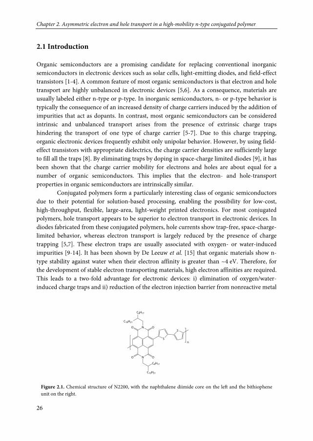
Figure 2.1. Chemical structure of N2200, with the naphthalene diimide core on the left and the bithiophene unit on the right.
N
N
S
SOO
OO
C10H21
C8H17
C8H17
C10H21
n
2.2 Electron Transport
27
electrodes. Recently, a high-mobility electron-transporting polymer (N2200) was developed,
consisting of a naphthalene diimide core (NDI), connected with a bithiophene unit (T-T), as displayed in Fig. 2.1 [16]. Apart from its high electron mobility, this polymer is particularly interesting because of its energy levels: the lowest unoccupied molecular orbital (LUMO) is located at ~-4 eV, while the highest occupied molecular orbital (HOMO) is situated at an energy of ~-5.6 eV [17]. This implies that the LUMO is low enough for stable, trap-free electron transport, while the HOMO is sufficiently shallow for efficient hole injection. As a result, N2200 is an ideal compound for a detailed investigation of both electron- and hole transport in a single material. In this chapter, we demonstrate trap-free electron and hole transport measurements in N2200, enabling direct evaluation of the charge-carrier mobilities. The electron mobility is observed to be more than two orders of magnitude higher than the hole mobility, which is supported by a quantum-chemical study. 2.2 Electron Transport Measurements on the bulk electron transport of N2200 have recently been carried out by Steyrleuthner et al. [18] In their report, a high electron mobility of 5 × 10⁻⁷ m2/Vs at room temperature was extracted from time-of-flight (TOF) measurements. Interestingly, the accompanying DC current measurements on electron-only diodes yielded considerably smaller values for the electron mobility. The apparent mobility was observed to increase with layer thickness, leading to the conclusion that the device current was injection limited, rather than limited by the bulk of the material. This is particularly surprising since the Fermi levels of the used cathode materials (e.g., barium) are expected to easily align with the low LUMO of N2200 to ensure Ohmic electron injection. Nevertheless, a convincing electric-field scaling of the current was presented for a wide range of layer thicknesses, which is characteristic of an injection-limited current. However, the origin of this behavior remained unclear. To enable a reliable investigation of the electron transport by means of single-carrier diodes, the problem of inefficient electron injection has to be overcome, so that true bulk-limited currents can be measured.
For the charge-transport measurements carried out in this study, single-carrier diodes were prepared. Electron-only diodes were fabricated, comprising a layer of N2200 sandwiched between an aluminum bottom and top electrode. To enhance electron injection from the top electrode, a Cs2CO3 layer (1 nm) was thermally evaporated on top of the polymer layer, prior to evaporation of the Al (100 nm) top electrode. Cs2CO3 has been frequently utilized as an efficient electron injection layer in polymer diodes [19-24]. Cesium carbonate decomposes into cesium oxides upon thermal evaporation and the resultant film is considered to be a heavily doped n-type semiconductor with an intrinsically low work function [24]. Therefore, thermally evaporated cesium carbonate exhibits good electron-injecting properties.
Chapter 2. Asymmetric electron and hole transport in a high-mobility n-type conjugated polymer
28
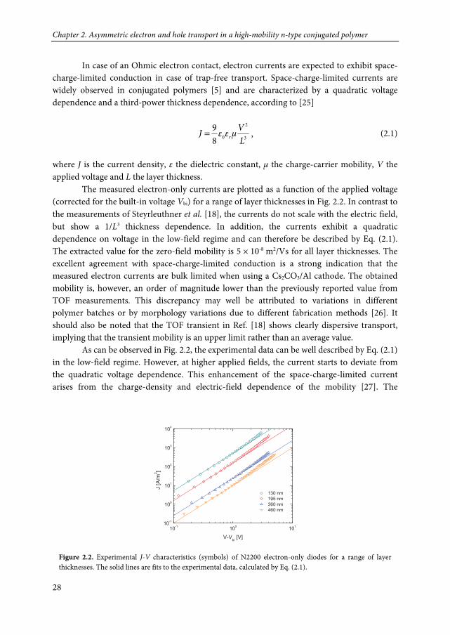
In case of an Ohmic electron contact, electron currents are expected to exhibit space-charge-limited conduction in case of trap-free transport. Space-charge-limited currents are widely observed in conjugated polymers [5] and are characterized by a quadratic voltage dependence and a third-power thickness dependence, according to [25]
3
2
089
LVμεεJ r= , (2.1)
where J is the current density, ε the dielectric constant, μ the charge-carrier mobility, V the applied voltage and L the layer thickness.
The measured electron-only currents are plotted as a function of the applied voltage (corrected for the built-in voltage Vbi) for a range of layer thicknesses in Fig. 2.2. In contrast to the measurements of Steyrleuthner et al. [18], the currents do not scale with the electric field, but show a 1/L3 thickness dependence. In addition, the currents exhibit a quadratic dependence on voltage in the low-field regime and can therefore be described by Eq. (2.1). The extracted value for the zero-field mobility is 5 × 10⁻⁸ m2/Vs for all layer thicknesses. The excellent agreement with space-charge-limited conduction is a strong indication that the measured electron currents are bulk limited when using a Cs2CO3/Al cathode. The obtained mobility is, however, an order of magnitude lower than the previously reported value from TOF measurements. This discrepancy may well be attributed to variations in different polymer batches or by morphology variations due to different fabrication methods [26]. It should also be noted that the TOF transient in Ref. [18] shows clearly dispersive transport, implying that the transient mobility is an upper limit rather than an average value.
As can be observed in Fig. 2.2, the experimental data can be well described by Eq. (2.1) in the low-field regime. However, at higher applied fields, the current starts to deviate from the quadratic voltage dependence. This enhancement of the space-charge-limited current arises from the charge-density and electric-field dependence of the mobility [27]. The
Figure 2.2. Experimental J-V characteristics (symbols) of N2200 electron-only diodes for a range of layer thicknesses. The solid lines are fits to the experimental data, calculated by Eq. (2.1).
2.2 Electron Transport
29
description of a charge-carrier density dependent mobility can be obtained from a numerical solution of the master equation for hopping transport in a disordered energy system with a Gaussian density-of-states (DOS) distribution. The field, density and temperature dependence of the mobility then follows from the choice of the width of the DOS distribution σ and the average intersite spacing a, as described by [28] ),(),(),,( ETfnTμEnTμ nn ≈ , (2.2) [ ]δ
n naσσTμnTμ )2)(ˆˆ(exp)(),( 3221
0 −= , (2.3)
( )2
2
ˆ4lnln)ˆˆln(2
σσσδ −−≡ , (2.4)
( )
−
+−= 18.012.2ˆ44.0exp),(
22/3
σEqaσETf , (2.5)
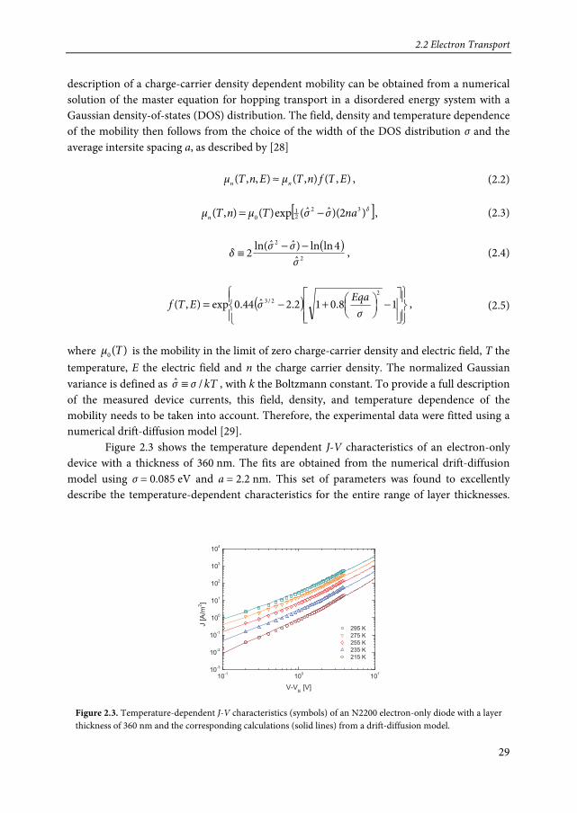
where )(0 Tμ is the mobility in the limit of zero charge-carrier density and electric field, T the temperature, E the electric field and n the charge carrier density. The normalized Gaussian variance is defined as kTσσ /ˆ ≡ , with k the Boltzmann constant. To provide a full description of the measured device currents, this field, density, and temperature dependence of the mobility needs to be taken into account. Therefore, the experimental data were fitted using a numerical drift-diffusion model [29].
Figure 2.3 shows the temperature dependent J-V characteristics of an electron-only device with a thickness of 360 nm. The fits are obtained from the numerical drift-diffusion model using σ = 0.085 eV and a = 2.2 nm. This set of parameters was found to excellently describe the temperature-dependent characteristics for the entire range of layer thicknesses.
Figure 2.3. Temperature-dependent J-V characteristics (symbols) of an N2200 electron-only diode with a layer thickness of 360 nm and the corresponding calculations (solid lines) from a drift-diffusion model.
Chapter 2. Asymmetric electron and hole transport in a high-mobility n-type conjugated polymer
30
The accurate agreement for the field, density and temperature dependence using a single set of parameters confirms the observation of bulk-limited electron currents. The width of the DOS distribution is considerably smaller than usually obtained for conjugated polymers, indicating a low degree of energetic disorder of the LUMO. The observation of weak disorder is in agreement with the high values obtained for the bulk electron mobility, together with its small temperature activation.
The good agreement of the current-voltage characteristics with Eq. (2.1) in the low field and density regime and the accurate description of the data with the numerical simulations show that electron transport is essentially trap free. However, when the charge concentration exceeds the trap density, the effect of traps becomes invisible in the current-voltage characteristics. This puts an upper limit on the trap density of about 5 × 10²¹ m-3 [30]. Although we cannot exclude the presence of a small shallow-trap concentration, it is clear that electron transport does not exhibit the distinct features of the usually observed trap-limited electron conduction in conjugated polymers [14]. 2.3 Hole transport Up to now, just a few conjugated polymers have exhibited both p-type and n-type conduction [31]. In the literature [16-18,26], N2200 has been essentially used as an electron transporting material and no hole conduction has been evidenced so far. As we have shown in the previous section, it is crucial to carefully choose the nature of the electrode in order to provide trap-free electron transport characterized in Fig. 2.2 by the quadratic voltage and third-power thickness dependence of the device current. It would be thus interesting to investigate now whether hole transport can be achieved; if it is also trap free in N2200, and how it compares to the obtained characteristics for electron transport.
To investigate the hole transport, hole-only diodes were prepared. Because of the relatively deep HOMO of N2200 (~-5.6 eV), a barrier for hole injection from common anodes such as gold (work function of 4.8 eV [32]) or poly(3,4-ethylenedioxythiophene):poly(styrene-sulfonic acid) (PEDOT:PSS), which has a work function of 5.0-5.2 eV [30,33,34], is expected. Recently, it was demonstrated that Ohmic charge injection can be achieved by using an MoO3 hole-injection layer for conjugated polymers comprising a HOMO as deep as -5.8 to -6.0 eV [35]. Thermally-evaporated molybdenum trioxide is an n-type semiconductor with a work function as high as 6.86 eV [36], resulting in good hole injection even for polymers with a deep HOMO. Therefore, hole-only diodes were fabricated with an MoO3(10 nm)/Al(100 nm) top electrode, using PEDOT:PSS-covered indium tin oxide as the bottom electrode. As expected, hole injection is considerably more efficient from MoO3 as compared to injection from the PEDOT:PSS counterelectrode. For MoO3 as Ohmic hole-injection contact, the hole currents exhibit a quadratic dependence on voltage and a 1/L3 thickness dependence, as displayed in Fig. 2.4. This is indicative of trap-free space-charge-limited hole transport, as also

2.3 Hole transport
31
observed previously for electron transport. By using Eq. (2.1), a zero-field hole mobility of 3.4 × 10⁻¹⁰ m2/Vs was determined.
As was done for the electron transport, numerical drift-diffusion simulations were carried out to fully describe the field, density, and temperature dependence of the hole transport. Figure 2.5 depicts the temperature dependent J-V characteristics of a hole-only device with a thickness of 140 nm. For all investigated layer thicknesses, the temperature dependent hole current could be accurately described with a single set of parameters. The extracted values for the DOS variance and the intersite spacing were σ = 0.13 eV and a = 1.3 nm, respectively. Apparently, hole transport is affected by significantly stronger disorder than electron transport. This is also reflected in the lower hole mobility, as compared to the electron mobility, as well as in the larger temperature activation for hole transport.
Figure 2.5. Temperature-dependent J-V characteristics (symbols) of an N2200 hole-only diode with a layer thickness of 140 nm and the corresponding calculations (solid lines) from a drift-diffusion model.
Figure 2.4. Experimental J-V characteristics (symbols) of N2200 hole-only diodes for a range of layer thicknesses. The solid lines are fits to the experimental data, calculated by Eq. (2.1).
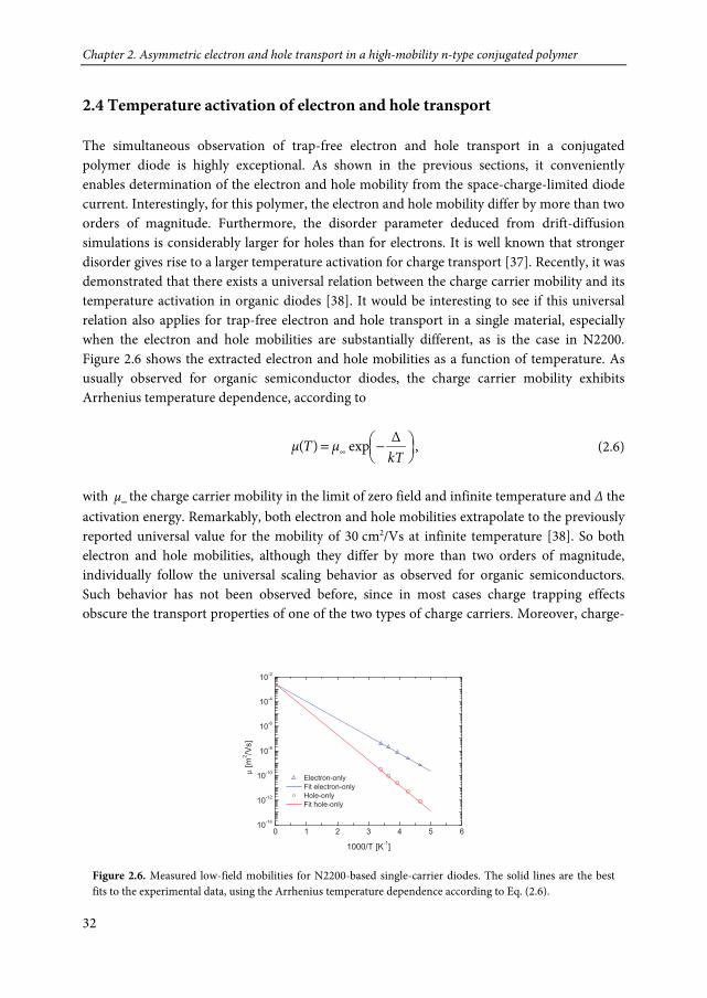
Chapter 2. Asymmetric electron and hole transport in a high-mobility n-type conjugated polymer
32
2.4 Temperature activation of electron and hole transport The simultaneous observation of trap-free electron and hole transport in a conjugated polymer diode is highly exceptional. As shown in the previous sections, it conveniently enables determination of the electron and hole mobility from the space-charge-limited diode current. Interestingly, for this polymer, the electron and hole mobility differ by more than two orders of magnitude. Furthermore, the disorder parameter deduced from drift-diffusion simulations is considerably larger for holes than for electrons. It is well known that stronger disorder gives rise to a larger temperature activation for charge transport [37]. Recently, it was demonstrated that there exists a universal relation between the charge carrier mobility and its temperature activation in organic diodes [38]. It would be interesting to see if this universal relation also applies for trap-free electron and hole transport in a single material, especially when the electron and hole mobilities are substantially different, as is the case in N2200. Figure 2.6 shows the extracted electron and hole mobilities as a function of temperature. As usually observed for organic semiconductor diodes, the charge carrier mobility exhibits Arrhenius temperature dependence, according to
−= ∞ kT
μTμ Δexp)( , (2.6)
with ∞μ the charge carrier mobility in the limit of zero field and infinite temperature and Δ the activation energy. Remarkably, both electron and hole mobilities extrapolate to the previously reported universal value for the mobility of 30 cm2/Vs at infinite temperature [38]. So both electron and hole mobilities, although they differ by more than two orders of magnitude, individually follow the universal scaling behavior as observed for organic semiconductors. Such behavior has not been observed before, since in most cases charge trapping effects obscure the transport properties of one of the two types of charge carriers. Moreover, charge-
Figure 2.6. Measured low-field mobilities for N2200-based single-carrier diodes. The solid lines are the best fits to the experimental data, using the Arrhenius temperature dependence according to Eq. (2.6).
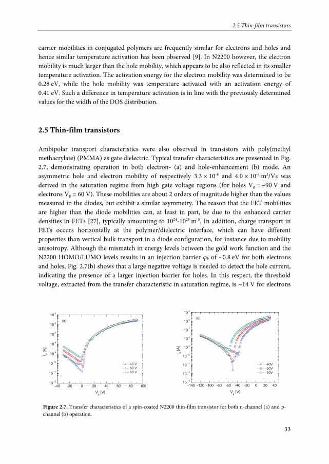
2.5 Thin-film transistors
33
carrier mobilities in conjugated polymers are frequently similar for electrons and holes and hence similar temperature activation has been observed [9]. In N2200 however, the electron mobility is much larger than the hole mobility, which appears to be also reflected in its smaller temperature activation. The activation energy for the electron mobility was determined to be 0.28 eV, while the hole mobility was temperature activated with an activation energy of 0.41 eV. Such a difference in temperature activation is in line with the previously determined values for the width of the DOS distribution. 2.5 Thin-film transistors Ambipolar transport characteristics were also observed in transistors with poly(methyl methacrylate) (PMMA) as gate dielectric. Typical transfer characteristics are presented in Fig. 2.7, demonstrating operation in both electron- (a) and hole-enhancement (b) mode. An asymmetric hole and electron mobility of respectively 3.3 × 10⁻⁸ and 4.0 × 10⁻⁶ m2/Vs was derived in the saturation regime from high gate voltage regions (for holes Vg = –90 V and electrons Vg = 60 V). These mobilities are about 2 orders of magnitude higher than the values measured in the diodes, but exhibit a similar asymmetry. The reason that the FET mobilities are higher than the diode mobilities can, at least in part, be due to the enhanced carrier densities in FETs [27], typically amounting to 1024-1025 m-3. In addition, charge transport in FETs occurs horizontally at the polymer/dielectric interface, which can have different properties than vertical bulk transport in a diode configuration, for instance due to mobility anisotropy. Although the mismatch in energy levels between the gold work function and the N2200 HOMO/LUMO levels results in an injection barrier φb of ~0.8 eV for both electrons and holes, Fig. 2.7(b) shows that a large negative voltage is needed to detect the hole current, indicating the presence of a larger injection barrier for holes. In this respect, the threshold voltage, extracted from the transfer characteristic in saturation regime, is ~14 V for electrons
Figure 2.7. Transfer characteristics of a spin-coated N2200 thin-film transistor for both n-channel (a) and p-channel (b) operation.
Chapter 2. Asymmetric electron and hole transport in a high-mobility n-type conjugated polymer
34
and ~–67 V for holes. 2.6 Quantum-chemical calculations Usually, electron and hole mobilities have similar values in conjugated homopolymers [8,9]. From the measurements on electron- and hole-only devices, it appears that the electron mobility is considerably higher than the hole mobility in the bulk of N2200. One of the reasons can certainly be found in the larger energetic disorder for hole transport as compared to electron transport. In addition, positional disorder as well as polaronic effects should also be considered in order to give an accurate picture of charge transport in this polymer [39]. These contributions are often difficult to assess experimentally since a reasonable description of the supramolecular morphology is required. To address this issue, quantum-chemical calculations have been carried out on model systems.
The two parameters characterizing charge transport in the hopping regime are the reorganization energy λ and the transfer integral J which appear explicitly in the expression of the Marcus charge-hopping rate as [40]
−=
kTλ
kTπλJ
hπk
4exp
412 2 , (2.7)
with h the reduced Planck constant. The reorganization energy λ is the sum of the internal reorganization energy λi, which accounts for the reorganization of the molecular geometry upon oxidation or reduction, and the external reorganization energy λS, which accounts for the change in the nuclear polarization of the molecules in the surrounding of the charge during the charge transfer process. From calculations on single crystals [41-43], it appears that the main contribution to the total reorganization energy is due to the geometric reorganization of the molecules involved in the charge transfer since the internal contribution is on the order of hundreds of meV while the external part is less than few tenths of meV.
In order to investigate the intrinsic charge transport properties of N2200, we have considered oligomers of N2200 going from 1 to 3 monomer units and have calculated their electronic structures and reorganization energies. The optimization of the geometry has been achieved at the Density Functional Theory (DFT) level with the hybrid functional B3LYP and the 6-31G** basis set. This methodology has been extensively used and has shown good agreement with experimental estimates of the reorganization energy [44]. 2.6.1 Torsion Potential Calculations Recently, X-ray scattering experiments [45] performed on N2200 thin films have revealed unconventional face-on stacking and a high-degree of in-plane crystallinity. It has been
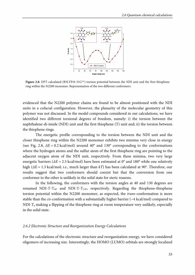
2.6 Quantum-chemical calculations
35
evidenced that the N2200 polymer chains are found to be almost positioned with the NDI units in a cofacial configuration. However, the planarity of the molecular geometry of this polymer was not discussed. In the model compounds considered in our calculations, we have identified two different torsional degrees of freedom, namely: i) the torsion between the naphthalene-di-imide (NDI) unit and the first thiophene (T) unit and; ii) the torsion between the thiophene rings.
The energetic profile corresponding to the torsion between the NDI unit and the closer thiophene ring within the N2200 monomer exhibits two minima very close in energy (see Fig. 2.8, ΔE = 0.2 kcal/mol) around 40° and 130° corresponding to the conformations where the hydrogen atoms and the sulfur atom of the first thiophene ring are pointing to the adjacent oxygen atom of the NDI unit, respectively. From these minima, two very large energetic barriers (ΔE = 2.5 kcal/mol) have been estimated at 0° and 180° while one relatively high (ΔE = 1.3 kcal/mol; i.e., much larger than kT) has been calculated at 90°. Therefore, our results suggest that two conformers should coexist but that the conversion from one conformer to the other is unlikely in the solid state for steric reasons.
In the following, the conformers with the torsion angles at 40 and 130 degrees are renamed NDI-T-T40° and NDI-T-T130°, respectively. Regarding the thiophene-thiophene torsion potential within the N2200 monomer, as expected, the trans-conformation is more stable than the cis-conformation with a substantially higher barrier (~4 kcal/mol) compared to NDI-T, making a flipping of the thiophene ring at room temperature very unlikely, especially in the solid state. 2.6.2 Electronic Structure and Reorganization Energy Calculations For the calculations of the electronic structure and reorganization energy, we have considered oligomers of increasing size. Interestingly, the HOMO (LUMO) orbitals are strongly localized
Figure 2.8. DFT-calculated (B3LYP/6-31G**) torsion potential between the NDI unit and the first thiophene ring within the N2200 monomer. Representation of the two different conformers.

Chapter 2. Asymmetric electron and hole transport in a high-mobility n-type conjugated polymer
36
on the electron-poor thiophene (electron-rich NDI) units, showing the strong donor and acceptor character difference between the NDI and bithiophene fragments (Fig. 2.9).
To estimate the reorganization energy, we have considered the initial conformation of the different oligomers corresponding to the energy minima obtained from the torsion potentials, namely, (either 40° or 130° for the NDI-T torsion and 165° (trans-conformation) for the thiophene-thiophene torsion angle).
For the monomers, the optimization of the different charged states has revealed quite different evolutions in the torsion angle, as shown in Table 2.1. The positive polaron exhibits large difference in torsion angle and tends to planarize the bithiophene unit while the negatively charged state is only slightly modified. The trans-conformation between the thiophene rings is kept.
The calculated reorganization energies (Table 2.2) for the positive polarons are larger as compared to the negative polarons for each of the systems considered. Two major reasons contribute to this difference: i) the number of atoms on which the HOMO and LUMO orbitals are delocalized; and ii) the amplitude of the change in the torsion angle between the neutral and charged states. Indeed, if more atoms are involved in the delocalization of an orbital, smaller bond length changes are expected upon oxidation/reduction, which hence reduces the internal reorganization energy while larger torsion angle differences between the neutral and charged compounds will lead to an increase in the internal reorganization energy. The difference in reorganization energy cannot be obviously explained on the basis of the
Figure 2.9. (a) HOMO and (b) LUMO orbitals for the N2200 dimer in its neutral state.
Neutral Positive Negative
NDI-T-T40 NDI-T torsion (°) 39 47 40
T-T torsion (°) 160 178 163
NDI-T-T130 NDI-T torsion (°) 125 47 120
T-T torsion (°) -157 -177 -160 Table 2.1: DFT-calculated (B3LYP/6-31G**) torsion angles between the different units in the two different conformers of the N2200 monomer in the neutral and charged states.

2.6 Quantum-chemical calculations
37
changes in bond lengths since they appear to be quite similar for both polaronic states (deviations of ~0.03 Å in agreement with references [46,47]). As illustrated for the monomer (Table 2.1) and confirmed for longer oligomers, the torsion angle difference between the neutral state and the polaronic state is larger for positive than negative polaron. These variations in torsion angles between both charged states are responsible for the difference in reorganization energy. Moreover, we have noticed that the internal reorganization energies associated to the negative polarons are similar for both conformers while the internal reorganization energies associated to the positive polarons are much smaller for NDI-T-T40 since going from the neutral state to the positive polaron of NDI-T-T130 involves larger changes in the torsion angles. 2.6.3 Transfer Integral Calculations The transfer integral J (i.e., electronic coupling) has often been estimated as half of the splitting of the HOMO (LUMO) levels in a neutral dimer for hole (electron) transport [48]. However, this approach is often biased by polarization effects, which in non-centrosymmetric structures create an energy offset of the electronic levels that does not contribute to the transfer efficiency [49,50]. Reliable values of J are thus obtained from the estimation of the direct interaction between the orbitals of the molecules involved in the charge transfer ( ≡jiψ ,
HOMO’s or LUMO’s) ji ψHψ || , with this matrix element calculated in an orthogonal }{ , jiψbasis set [49,51].
Since the transfer integral is highly sensitive to the relative orientation of the molecules [39], it is of utmost importance to have a reasonable model for the packing of the polymer chains involved in the charge transport. Recently, a model of the packing of the NDI-T-T polymer chains has been elaborated from X-ray scattering measurements [45], suggesting that the chains are superimposed. Starting from this model, displacements along the polymer axis lead to energetically unfavorable packings. Therefore, the polymer chains are clicked due
n = 1 n = 2 n = 3
(NDI-T-T40)n hiλ (eV) 0.32 0.24 0.16 eiλ (eV) 0.28 0.16 0.12
(NDI-T-T130)n hiλ (eV) 0.46 0.38 0.27 eiλ (eV) 0.29 0.19 0.14
Table 2.2: Hole ( hiλ ) and electron ( e
iλ ) internal reorganization energies calculated for both conformers of increasing length.
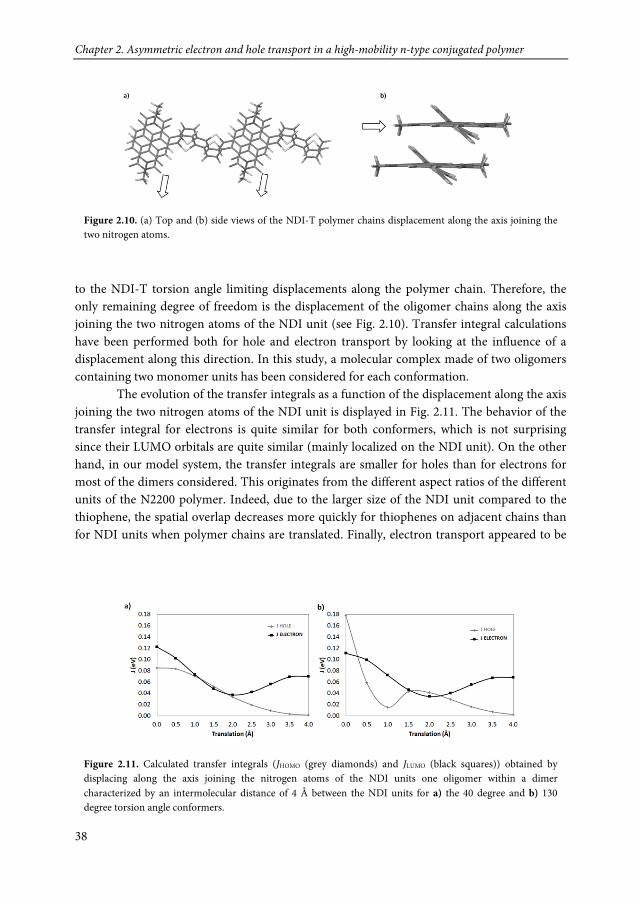
Chapter 2. Asymmetric electron and hole transport in a high-mobility n-type conjugated polymer
38
to the NDI-T torsion angle limiting displacements along the polymer chain. Therefore, the only remaining degree of freedom is the displacement of the oligomer chains along the axis joining the two nitrogen atoms of the NDI unit (see Fig. 2.10). Transfer integral calculations have been performed both for hole and electron transport by looking at the influence of a displacement along this direction. In this study, a molecular complex made of two oligomers containing two monomer units has been considered for each conformation.
The evolution of the transfer integrals as a function of the displacement along the axis joining the two nitrogen atoms of the NDI unit is displayed in Fig. 2.11. The behavior of the transfer integral for electrons is quite similar for both conformers, which is not surprising since their LUMO orbitals are quite similar (mainly localized on the NDI unit). On the other hand, in our model system, the transfer integrals are smaller for holes than for electrons for most of the dimers considered. This originates from the different aspect ratios of the different units of the N2200 polymer. Indeed, due to the larger size of the NDI unit compared to the thiophene, the spatial overlap decreases more quickly for thiophenes on adjacent chains than for NDI units when polymer chains are translated. Finally, electron transport appeared to be
Figure 2.10. (a) Top and (b) side views of the NDI-T polymer chains displacement along the axis joining the two nitrogen atoms.
Figure 2.11. Calculated transfer integrals (JHOMO (grey diamonds) and JLUMO (black squares)) obtained by displacing along the axis joining the nitrogen atoms of the NDI units one oligomer within a dimer characterized by an intermolecular distance of 4 Å between the NDI units for a) the 40 degree and b) 130 degree torsion angle conformers.

2.7 Conclusions
39
less sensitive to displacements than hole transport in agreement with a recent theoretical study using a similar methodology on different N2200 structures [46,47].
The larger spread in the transfer integral for holes as a function of displacements can be interpreted as larger positional disorder. In terms of the Gaussian disorder model, this would be reflected in a larger width of the Gaussian DOS distribution of the HOMO as compared to the LUMO. This is in agreement with larger disorder parameter σ for holes that was extracted from modeling the experimental current-voltage characteristics of hole-only diodes with the extended Gaussian disorder model [28] as done in previous sections. In addition, the larger reorganization energy, in combination with larger positional disorder, will lead to a higher temperature activation for hole transport, which has been observed experimentally. In the end, looking back at the expression for the Marcus charge-transfer rate [Eq. (2.7)], it appears that the hopping rate is maximized for a large transfer integral and a small reorganization energy. As a result, electron transport has to be intrinsically better than hole transport under the same charge injection and extraction conditions. 2.7 Conclusions In conclusion, we found intrinsically asymmetric bulk electron and hole transport in the n-type polymer N2200. Electron- and hole-only devices of N2200 were fabricated and Ohmic electron and hole contacts were demonstrated. Remarkably, both electron and hole currents showed trap-free space-charge-limited behavior. As a result of the unusual absence of extrinsic charge traps for both types of charge carriers, intrinsic charge-transport properties could be evaluated. Room-temperature mobilities of 5 × 10⁻⁸ m2/Vs for electrons and 3.4 × 10⁻¹⁰ m2/Vs for holes were determined for the bulk transport through the polymer. Furthermore, electron and hole transport was observed to follow universal Arrhenius temperature scaling with an activation energy of 0.28 eV and 0.41 eV, respectively. Such temperature scaling for both electrons and holes could not be observed before in a single organic semiconductor, since transport of one of the two carriers is usually obscured by trapping effects. The large difference between electron and hole transport was rationalized by quantum-chemical calculations, which revealed that the internal reorganization energy is smaller and the transfer integral is larger for electrons as compared to holes. As a consequence, electron transport is intrinsically better than hole transport, when the same injection and extraction conditions are considered. Experimental Section The polymer poly{[N,N'-bis(2-octyldodecyl)-naphthalene-1,4,5,8-bis(dicarboximide)-2,6-diyl]-alt-5,5'-(2,2'-dithiophene)} [P(NDI2OD-T2), Polyera ActivInk™ N2200] was obtained
Chapter 2. Asymmetric electron and hole transport in a high-mobility n-type conjugated polymer
40
from Polyera Corporation and used as received. Sandwich-type devices were fabricated on top of thoroughly cleaned glass substrates and glass substrates prepatterned with indium-tin oxide (ITO). Electron-only devices were fabricated by evaporating an Al crossbar structure on cleaned glass substrates as a non-injecting bottom contact. Subsequently, a layer of N2200 was spin cast from toluene solution under N2 atmosphere. The devices were finished by thermal evaporation of a Cs2CO3(1 nm)/Al(100 nm) cathode in vacuum (1 × 10⁻⁶ mbar). For the hole-only devices, cleaned glass/ITO substrates were spin coated with a layer of PEDOT:PSS with a thickness of 60 nm, which was used to block the injection of electrons. Next, the N2200 layer was applied by spin coating and an MoO3(10 nm)/Al(100 nm) anode was evaporated subsequently. Electron- and hole-only devices were not exposed to air from the moment of depositing the N2200 layer until finishing the electrical measurements. Electrical measurements on the sandwich-type devices were conducted under controlled N2 atmosphere, using a computer-controlled Keithley 2400 source meter.
Thin-film transistors in staggered top-gate geometry were fabricated by spin-coating the semiconductor solution (10 mg mL-1) on glass substrates with bottom Au contacts (channel dimensions of W = 500 μm and L = 50 μm). After spinning the active layer, samples were annealed in vacuum oven at 120 °C overnight. The poly(methyl methacrylate) (PMMA) top-gate dielectric was spin coated from an 80 mg mL-1 ethyl acetate solution at 1000 rpm (700-800 nm, k = 3.6) and annealed at 120 °C for 2 h. Deposition of the top Al gate electrode completed the staggered thin-film transistors. The current-voltage characteristics were measured in air at room temperature using a Keithley 4200-SCS semiconductor parameter analyzer and mobility was evaluated in the saturation regime.

References
41
References
[1] C. W. Tang and S. A. VanSlyke, Appl. Phys. Lett. 51, 913 (1987).
[2] J. H. Burroughes, D. D. C. Bradley, A. R. Brown, R. N. Marks, K. Mackay, R. H. Friend, P. L. Burns, and A. B. Holmes, Nature 347, 539 (1990).
[3] G. Yu, J. Gao, J. C. Hummelen, F. Wudl, and A. J. Heeger, Science 270, 1789 (1995).
[4] H. Klauk, Chem. Soc. Rev. 39, 2643 (2010).
[5] P. W. M. Blom, M. J. M. de Jong, and J. J. M. Vleggaar, Appl. Phys. Lett. 68, 3308 (1996).
[6] J. Zaumseil and H. Sirringhaus, Chem. Rev. 107, 1296 (2007).
[7] M. M. Mandoc, B. de Boer, G. Paasch, and P. W. M. Blom, Phys. Rev. B 75, 193202 (2007).
[8] L. L. Chua, J. Zaumseil, J. F. Chang, E. C. W. Ou, P. K. H. Ho, H. Sirringhaus, and R. H. Friend, Nature 434, 194 (2005).
[9] Y. Zhang, B. de Boer, and P. W. M. Blom, Phys. Rev. B 81, 085201 (2010).
[10] H.-E. Tseng, K.-Y. Peng, and S.-A. Chen, Appl. Phys. Lett. 82, 4086 (2003).
[11] V. Kažukauskas, Semicond. Sci. Technol. 19, 1373 (2004).
[12] T. D. Anthopoulos, G. C. Anyfantis, G. C. Papavassiliou, and D. M. de Leeuw, Appl. Phys. Lett. 90, 122105 (2007).
[13] J.-M. Zhuo, L.-H. Zhao, R.-Q. Png, L.-Y. Wong, P.-J. Chia, J.-C. Tang, S. Sivaramakrishnan, M. Zhou, E. C.-W. Ou, S.-J. Chua, W.-S., Sim, L.-L. Chua, and P. K.-H. Ho, Adv. Mater. 21, 4747 (2009).
[14] H. T. Nicolai, M. Kuik, G. A. H. Wetzelaer, B. de Boer, C. Campbell, C. Risko, J. L. Brédas, and P. W. M. Blom, Nat. Mater. 11, 882 (2012).
[15] D. M. de Leeuw, M. M. J. Simenon, A. R. Brown, and R. E. F. Einerhand, Synth. Met. 87, 53 (1997).
[16] Z. Chen, Y. Zheng, H. Yan, and A. Facchetti, J. Am. Chem. Soc. 131, 8 (2009).
[17] H. Yan, Z. Chen, Y. Zheng, C. Newman, J. R. Quinn, F. Dötz, M. Kastler, and A. Facchetti, Nature 457, 679 (2009).
Chapter 2. Asymmetric electron and hole transport in a high-mobility n-type conjugated polymer
42
[18] R. Steyrleuthner, M. Schubert, F. Jaiser, J. C. Blakesley, Z. Chen, A. Facchetti, and D. Neher, Adv. Mater. 22, 2799 (2010).
[19] T. Hasegawa, S. Miura, T. Moriyama, T. Kimura, I. Takaya, Y. Osato, and H. Mizutani, SID Int. Symp. Digest. Tech. Papers 35, 154 (2004).
[20] J. Huang, G. Li, E. Wu, Q. Xu, and Y. Yang, Adv. Mater. 18, 114 (2006).
[21] C. Wu, C. T. Lin, Y. Chen, M. Chen, Y. Lu, and C. C. Wu, Appl. Phys. Lett. 88, 152104 (2006).
[22] H. J. Bolink, E. Coronado, J. Orozco, and M. Sessolo, Adv. Mater. 21, 79 (2009).
[23] D. Kabra, L. P. Lu, M. H. Song, H. J. Snaith, and R. H. Friend, Adv. Mater. 22, 29 (2010).
[24] J. Huang, Z. Xu, and Y. Yang, Adv. Funct. Mater. 17, 1966 (2007).
[25] N. F. Mott and R. W. Gurney, Electronic Processes in Ionic Crystals (Oxford University Press, London, 1940).
[26] J. C. Blakesley, M. Schubert, R. Steyrleuthner, Z. Chen, A. Facchetti, and D. Neher, Appl. Phys. Lett. 99, 183310 (2011).
[27] C. Tanase, E. J. Meijer, P. W. M. Blom, and D. M. de Leeuw, Phys. Rev. Lett. 91, 216601 (2003).
[28] W. F. Pasveer, J. Cottaar, C. Tanase, R. Coehoorn, P. A. Bobbert, P. W. M. Blom, D. M. de Leeuw, and M. A. J. Michels, Phys. Rev. Lett. 94, 206601 (2005).
[29] L. J. A. Koster, E. C. P. Smits, V. D. Mihailetchi, and P. W. M. Blom, Phys. Rev. B 72, 085205 (2005).
[30] N. I. Craciun, J. J. Brondijk, and P. W. M. Blom, Phys. Rev. B 77, 035206 (2008).
[31] Z. Chen, M. J. Lee, R. S. Ashraf, Y. Gu, S. Albert-Seifried, M. M. Meedom Nielsen, B. Schroeder, T. D. Anthopoulos, M. Heeney, I. McCulloch, and H. Sirringhaus, Adv. Mater. 24, 647 (2012).
[32] K. Asadi, T. G. de Boer, P. W. M. Blom, and D. M. de Leeuw, Adv. Funct. Mater. 19, 3173 (2009).
[33] N. Koch, A. Vollmer, and A. Elschner, Appl. Phys. Lett. 90, 043512 (2007).
[34] T.-W. Lee, Y. Chung, O. Kwon, and J.-J. Park, Adv. Funct. Mater. 17, 390 (2007).
References
43
[35] H. T. Nicolai, G. A. H. Wetzelaer, M. Kuik, A. J. Kronemeijer, B. de Boer, and P. W. M. Blom, Appl. Phys. Lett. 96, 172107 (2010).
[36] M. Kröger, S. Hamwi, J. Meyer, T. Riedl, W. Kowalsky, and A. Kahn, Org. Electron. 10, 932 (2009).
[37] H. Bässler, Phys. Status Solidi B 175, 15 (1993).
[38] N. I. Craciun, J. Wildeman, and P. W. M. Blom, Phys. Rev. Lett. 100, 056601 (2008).
[39] J. L. Brédas, J. P. Calbert, D. A. da Silva Filho, and J. Cornil, Proc. Natl. Acad. Sci. U.S.A. 99, 5804 (2002).
[40] R. A. Marcus, Rev. Mod. Phys. 65, 599 (1993).
[41] N. Martinelli, J. Idé, R.S. Sanchez-Carrera, V. Coropceanu, J. L. Brédas, L. Ducasse, F. Castet, J. Cornil, and D. Beljonne. J. Phys. Chem. C 114, 20678 (2010).
[42] J. E. Norton and J. L. Brédas, J. Am. Chem. Soc. 130, 12377 (2008).
[43] D. P. MacMahon and A. Troisi, J. Phys. Chem. Lett. 1, 941 (2010).
[44] V. Coropceanu, M. Malagoli, D. A. da Silva Filho, N. E. Gruhn, T. G. Bill, and J. L. Brédas, Phys. Rev. Lett. 89, 275503 (2002).
[45] J. Rivnay, M. F. Toney, Y. Zheng, I. V. Kauvar, Z. Chen, V. Wagner, A. Facchetti, and A. Salleo., Adv. Mat. 22, 4359 (2010).
[46] M. Caironi, M. Bird, D. Fazzi, Z. Chen, R. Di Pietro, C. Newman, A. Facchetti, and H. Sirringhaus, Adv. Funct. Mat. 21, 3371 (2011).
[47] D. Fazzi, M. Caironi, and C. Castiglioni, J. Am. Chem. Soc. 133, 19056 (2011).
[48] J. L. Brédas, D. Beljonne, V. Coropceanu, and J. Cornil, Chem. Rev. 104, 4971 (2004).
[49] E. F. Valeev, V. Coropceanu, D. A. d. Silva, S. Salman, and J. L. Brédas, J. Am. Chem. Soc. 128, 9882 (2006).
[50] A. Van Vooren, V. Lemaur, A. Ye, D. Beljonne, and J. Cornil, Chem. Phys. Chem. 8, 1240 (2007).
[51] L. Viani, Y. Olivier, S. Athanasopoulos, D.A. da Silva Filho, J. Hulliger, J.L. Brédas, J. Gierschner, and J. Cornil, ChemPhysChem 11, 1062 (2010).

45
Trap-assisted and Langevin-type recombination in organic light-emitting diodes Trapping of charges is known to play an important role in the charge transport of
organic semiconductors, but the role of traps in the recombination process has not been addressed. In this chapter, we show that the ideality factor of the current of organic light-emitting diodes (OLEDs) in the diffusion-dominated regime has a temperature independent value of 2, which reveals that nonradiative trap-assisted recombination is dominating the current. In contrast, the ideality factor of the light output approaches unity, demonstrating that the luminance is governed by recombination of the bimolecular Langevin type. This apparent contradiction can be resolved by measuring the current and luminance ideality factor for a white-emitting polymer, where both free and trapped charge carriers recombine radiatively. With increasing bias voltage, Langevin recombination becomes dominant over the trap-assisted recombination due to its stronger dependence on carrier density, leading to an enhancement of the OLED efficiency.
3. Trap-assisted and Langevin-type recombination in organic light-emitting diodes
3
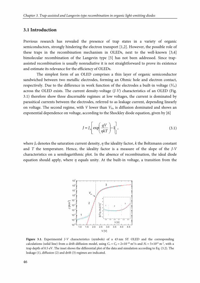
Chapter 3. Trap-assisted and Langevin-type recombination in organic light-emitting diodes
46
3.1 Introduction Previous research has revealed the presence of trap states in a variety of organic semiconductors, strongly hindering the electron transport [1,2]. However, the possible role of these traps in the recombination mechanism in OLEDs, next to the well-known [3,4] bimolecular recombination of the Langevin type [5] has not been addressed. Since trap-assisted recombination is usually nonradiative it is not straightforward to prove its existence and estimate its relevance for the efficiency of OLEDs.
The simplest form of an OLED comprises a thin layer of organic semiconductor sandwiched between two metallic electrodes, forming an Ohmic hole and electron contact, respectively. Due to the difference in work function of the electrodes a built-in voltage (Vbi) across the OLED exists. The current density-voltage (J-V) characteristics of an OLED (Fig. 3.1) therefore show three discernable regimes: at low voltages, the current is dominated by parasitical currents between the electrodes, referred to as leakage current, depending linearly on voltage. The second regime, with V lower than Vbi, is diffusion dominated and shows an exponential dependence on voltage, according to the Shockley diode equation, given by [6]
−
= 1exp0 kTη
qVJJ , (3.1)
where J0 denotes the saturation current density, η the ideality factor, k the Boltzmann constant and T the temperature. Hence, the ideality factor is a measure of the slope of the J-V characteristics on a semilogarithmic plot. In the absence of recombination, the ideal diode equation should apply, where η equals unity. At the built-in voltage, a transition from the
Figure 3.1. Experimental J-V characteristics (symbols) of a 43 nm SY OLED and the corresponding calculations (solid line) from a drift-diffusion model, using Cn = Cp = 2×10-18 m3/s and Nt = 5×10²² m-3, with a trap depth of 0.5 eV. The inset shows the differential plot of the data and simulation according to Eq. (3.2). The leakage (1), diffusion (2) and drift (3) regimes are indicated.
3.2 Ideality factor of an OLED
47
exponential regime to the drift-dominated, space-charge-limited regime occurs [1], which is characterized by a quadratic dependence of the current on the voltage in the case of trap-free transport, according to the Mott-Gurney square law [7].
As first described by Sah et al., the ideality factor of a classical p-n junction is affected by trap-assisted recombination in the space-charge region [8]. Here, electrons immobilized in trapping sites recombine with free holes as described by the Shockley-Read-Hall (SRH) formalism [9,10]. When SRH recombination is the dominant loss mechanism, the ideality factor is expected to be exactly equal to 2 [8]. As a result, the ideality factor can be used as a fingerprint for trap-assisted recombination. In this chapter, we demonstrate that the diode characteristics and ideality factor for a variety of conjugated polymers are dominated by trap-assisted recombination, whereas the luminance is governed by Langevin recombination. In addition, we show that the guest emission in a host-guest system can be accurately described by an SRH process. 3.2 Ideality factor of an OLED In this chapter, the OLEDs were prepared on top of a glass substrate, patterned with a transparent indium-tin oxide electrode. As organic semiconductors, a variety of conjugated polymers have been used. As anode and cathode, spin-casted poly(3,4-ethylenedioxy-thiophene):poly(styrenesulfonic acid) (PEDOT:PSS; Clevios CH8000) and thermally- evaporated Ba(5 nm)/Al(100 nm) were used, respectively. A voltage sweep of a typical OLED is depicted in Fig. 3.1, where the poly(p-phenylene vinylene) (PPV) derivative Super Yellow (SY) was used as emitter. As the present study focuses on the ideality factor, the slope of the diffusion regime below Vbi is of predominant interest. Conventionally, the ideality factor is determined by fitting the experimental data with Eq. (3.1). However, in order to prevent erroneous fitting, we determine the ideality factor by numerical differentiation according to
1
ln−
∂
∂=V
Jq
kTη . (3.2)
By plotting this quantity against voltage, as shown in the inset of Fig. 3.1, the three regimes in the J-V characteristics can be distinguished again, where the ideality factor is obtained from the plateau value. The plateau value can be regarded as the steepest exponential incline of the J-V characteristics. For a correct determination of the ideality factor it is of paramount importance that the exponential part is clearly discernable, requiring low leakage currents and high current densities in the space-charge limit. The latter can be achieved for materials with a high charge-carrier mobility or by decreasing the layer thickness.
As can be seen in Fig. 3.1, an ideality factor of 2 was determined for the SY device, in exact correspondence to the value that is predicted from the Sah-Noyce-Shockley theory [8] in the case of trap-assisted recombination. In addition, both the drift and diffusion regimes can
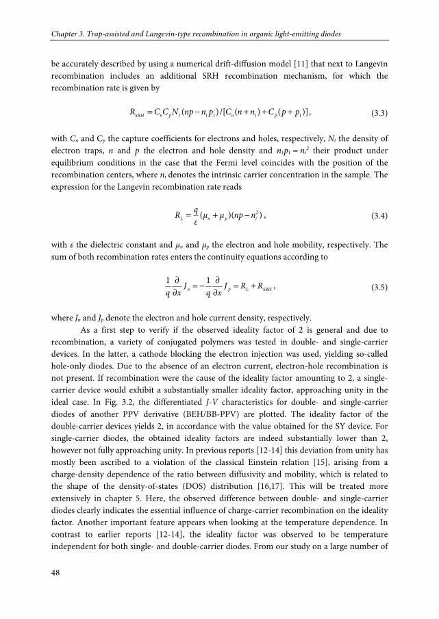
Chapter 3. Trap-assisted and Langevin-type recombination in organic light-emitting diodes
48
be accurately described by using a numerical drift-diffusion model [11] that next to Langevin recombination includes an additional SRH recombination mechanism, for which the recombination rate is given by )]()(/[)( 1111 ppCnnCpnnpNCCR pntpnSRH +++−= , (3.3) with Cn and Cp the capture coefficients for electrons and holes, respectively, Nt the density of electron traps, n and p the electron and hole density and n1p1 = ni
2 their product under equilibrium conditions in the case that the Fermi level coincides with the position of the recombination centers, where ni denotes the intrinsic carrier concentration in the sample. The expression for the Langevin recombination rate reads
))(( 2ipnL nnpμμ
εqR −+= , (3.4)
with ε the dielectric constant and μn and μp the electron and hole mobility, respectively. The sum of both recombination rates enters the continuity equations according to
SRHLpn RRJxq
Jxq
+=∂∂−=
∂∂ 11 , (3.5)
where Jn and Jp denote the electron and hole current density, respectively.
As a first step to verify if the observed ideality factor of 2 is general and due to recombination, a variety of conjugated polymers was tested in double- and single-carrier devices. In the latter, a cathode blocking the electron injection was used, yielding so-called hole-only diodes. Due to the absence of an electron current, electron-hole recombination is not present. If recombination were the cause of the ideality factor amounting to 2, a single-carrier device would exhibit a substantially smaller ideality factor, approaching unity in the ideal case. In Fig. 3.2, the differentiated J-V characteristics for double- and single-carrier diodes of another PPV derivative (BEH/BB-PPV) are plotted. The ideality factor of the double-carrier devices yields 2, in accordance with the value obtained for the SY device. For single-carrier diodes, the obtained ideality factors are indeed substantially lower than 2, however not fully approaching unity. In previous reports [12-14] this deviation from unity has mostly been ascribed to a violation of the classical Einstein relation [15], arising from a charge-density dependence of the ratio between diffusivity and mobility, which is related to the shape of the density-of-states (DOS) distribution [16,17]. This will be treated more extensively in chapter 5. Here, the observed difference between double- and single-carrier diodes clearly indicates the essential influence of charge-carrier recombination on the ideality factor. Another important feature appears when looking at the temperature dependence. In contrast to earlier reports [12-14], the ideality factor was observed to be temperature independent for both single- and double-carrier diodes. From our study on a large number of
3.3 Luminance ideality factor
49
organic diodes we found that a temperature dependent ideality factor is an experimental artifact that is caused by a too large leakage current (regime 1). In that case, the leakage current masks the diffusion regime as the drift current reduces upon cooling due to the temperature dependence of the mobility [18] and the plateau cannot be discerned anymore. The apparent ideality factor will then be too high and temperature dependent. For materials with a high charge-carrier mobility, and hence comprising a weakly temperature-activated transport [18], we observed a temperature-independent ideality factor down to 215 K with a variance of less than 0.05. The temperature independence of the ideality factor corresponds with the conventional Shockley diode equation and contradicts the proposed invalidity of the classical Einstein relation [12,17]. This observation further supports the dominance of trap-assisted recombination on the ideality factor in OLEDs. In our study, the temperature independence as well as similar magnitudes for η were also obtained for other classes of conjugated polymers, including polyfluorenes, polythiophenes, polyspirobifluorenes, polytriarylamines, as well as fullerene derivatives. 3.3 Luminance ideality factor As stated in the previous section, an ideality factor of 2 in the current of an OLED can be explained by the fact that the dominant recombination mechanism is trap assisted. However, previous studies [3,4] concluded that charge recombination in organic semiconductors is a bimolecular process of the Langevin type [5], controlled by the diffusion of oppositely-charged free carriers towards each other in their mutual coulomb field. This apparent discrepancy can be resolved by also studying the ideality factor of the luminance (L) vs. voltage characteristics, analogous to the case for the current density. An important requirement to reliably extract such a luminance ideality factor is a sufficient luminous
Figure 3.2. Temperature-dependent η-V characteristics of single- and double-carrier diodes of a PPV derivative. The difference between single- and double-carrier diodes shows that recombination plays an essential role.

Chapter 3. Trap-assisted and Langevin-type recombination in organic light-emitting diodes
50
efficiency, as the length of the exponential regime is limited by the sensitivity of the photodiode used to record the light output. When plotting the ideality factors of the current and the luminance (Fig. 3.3), it appears that a distinct dissimilarity in the slope of the exponential part of the characteristics is present. In contrast to case for the current density (η = 2), the ideality factor determined from the L-V characteristics approaches unity, being consistent with Langevin recombination. This is a strong indication that in these diodes nonradiative trap-assisted recombination is the most dominant and controls the current, whereas the light emission is a result of a competing bimolecular recombination process.
In order to experimentally verify this hypothesis, we studied the L-V characteristics of a diode in which emissive recombination from trapped charge carriers is present, as is the case in host-guest systems, frequently applied in highly-efficient organic LEDs. An ideal compound for this test is a state-of-the-art white-emitting polymer (Merck) [19], where green- and red-emitting chromophores are incorporated in the blue-emitting backbone. In this polymer, the highest occupied molecular orbital (HOMO) levels of the chromophores align with the HOMO of the blue host, whereas the lowest unoccupied molecular orbital (LUMO) levels of the chromophores are substantially below the LUMO of the blue host due to the smaller band gap [20]. The chromophores are therefore expected to trap electrons. Hence, the blue part of the emission spectrum is assumed to arise from Langevin recombination, whereas the red emission can be ascribed to recombination of holes with electrons that are trapped on the chromophore. By measuring the L-V characteristics through selective optical filters, the different recombination mechanisms may be disentangled. Therefore, a blue dichroic filter (serving as a bandpass filter) and a 550 nm longpass filter were used, splitting the electroluminescence (EL) spectrum in a blue and red component. As can be observed in Fig. 3.4(a), the ideality factor of the current density again amounts to 2, consistent with materials without chromophores. Remarkably, Fig. 3.4(b) shows a clear difference in the slope of the L-V characteristics when either the red or blue part of the spectrum is measured.
Figure 3.3. η-V characteristics of SY and NRS-PPV OLEDs derived from the current and the luminance. The luminance ideality factor approaching unity indicates that light-emission is governed by a Langevin process. The inset shows a schematic representation of the recombination mechanisms.
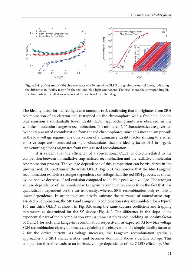
3.3 Luminance ideality factor
51
The ideality factor for the red light also amounts to 2, confirming that it originates from SRH recombination of an electron that is trapped on the chromophore with a free hole. For the blue emission a substantially lower ideality factor approaching unity was observed, in line with the bimolecular Langevin recombination. The unfiltered L-V characteristics are governed by the trap-assisted recombination from the red chromophores, since this mechanism prevails in the low voltage regime. The observation of a luminance ideality factor shifting to 2 when emissive traps are introduced strongly substantiates that the ideality factor of 2 in organic light-emitting diodes originates from trap-assisted recombination.
It is evident that the efficiency of a conventional OLED is directly related to the competition between nonradiative trap-assisted recombination and the radiative bimolecular recombination process. The voltage dependence of this competition can be visualized in the (normalized) EL spectrum of the white OLED (Fig. 3.5). We observe that the blue Langevin recombination exhibits a stronger dependence on voltage than the red SRH process, as shown by the relative decrease of red emission compared to the blue peak with voltage. The stronger voltage dependence of the bimolecular Langevin recombination arises from the fact that it is quadratically dependent on the carrier density, whereas SRH recombination only exhibits a linear dependence. In order to quantitatively estimate the relevance of nonradiative trap-assisted recombination, the SRH and Langevin recombination rates are simulated for a typical 100 nm thick OLED as shown in Fig. 3.6, using the same capture coefficient and trapping parameters as determined for the SY device (Fig. 3.1). The difference in the slope of the exponential part of the recombination rates is immediately visible, yielding an ideality factor of 2 and 1 for SRH and Langevin recombination respectively, as expected. At low bias voltage SRH recombination clearly dominates, explaining the observation of a simple ideality factor of 2 for the device current. As voltage increases, the Langevin recombination gradually approaches the SRH characteristics, and becomes dominant above a certain voltage. This competition therefore leads to an intrinsic voltage dependence of the OLED efficiency. Until
Figure 3.4. η-V (a) and L-V (b) characteristics of a 30 nm white OLED using selective optical filters, indicating the difference in ideality factor for the red- and blue-light component. The inset shows the corresponding EL spectrum, where the filled areas represent the spectra of the filtered light.
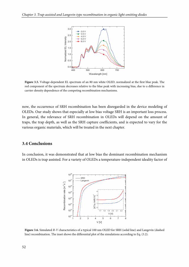
Chapter 3. Trap-assisted and Langevin-type recombination in organic light-emitting diodes
52
now, the occurrence of SRH recombination has been disregarded in the device modeling of OLEDs. Our study shows that especially at low bias voltage SRH is an important loss process. In general, the relevance of SRH recombination in OLEDs will depend on the amount of traps, the trap depth, as well as the SRH capture coefficients, and is expected to vary for the various organic materials, which will be treated in the next chapter. 3.4 Conclusions In conclusion, it was demonstrated that at low bias the dominant recombination mechanism in OLEDs is trap assisted. For a variety of OLEDs a temperature-independent ideality factor of
Figure 3.5. Voltage-dependent EL spectrum of an 80 nm white OLED, normalized at the first blue peak. The red component of the spectrum decreases relative to the blue peak with increasing bias, due to a difference in carrier-density dependence of the competing recombination mechanisms.
Figure 3.6. Simulated R-V characteristics of a typical 100 nm OLED for SRH (solid line) and Langevin (dashed line) recombination. The inset shows the differential plot of the simulations according to Eq. (3.2).
3.4 Conclusions
53
2 for the current was determined, which evidences the presence of SRH recombination from trapping sites. In line with this finding, the ideality factor shifts towards unity in the absence of recombination. Furthermore, an ideality factor approaching unity was also determined for the luminance, showing that the emissive recombination is determined by a bimolecular Langevin process, and that recombination from trapping sites is nonradiative. This was further confirmed by selectively filtering the blue and red part of the EL spectrum of a white OLED, where red chromophores incorporated in the blue backbone function as emissive traps, allowing disentanglement of both competing recombination mechanisms by measuring the luminance ideality factor. Drift-diffusion simulations show that with increasing bias Langevin recombination becomes more dominant, which is also reflected in the voltage-dependent emission spectrum of a white OLED.
Our study shows that the ideality factor can be regarded as an effective tool for studying the recombination mechanisms in OLEDs, for both single-color and white-emitting devices. Accurate determination and understanding of the recombination processes is essential for identifying nonradiative loss mechanisms and thereby giving new insights for improving the OLED efficiency.
Chapter 3. Trap-assisted and Langevin-type recombination in organic light-emitting diodes
54
References
[1] P. W. M. Blom, M. J. M. de Jong, and J. J. M. Vleggaar, Appl. Phys. Lett. 68, 3308 (1996).
[2] M. M. Mandoc, B. de Boer, G. Paasch, and P. W. M. Blom, Phys. Rev. B. 75, 193202 (2007).
[3] P. W. M. Blom, M. J. M. de Jong, and S. Breedijk, Appl. Phys. Lett. 71, 930 (1997).
[4] A. Pivrikas, G. Juška, R. Österbacka, M. Westerling, M. Viliūnas, K. Arlauska, and H. Stubb, Phys. Rev. B 71, 125205 (2005).
[5] P. Langevin, Ann. Chim. Phys. 28, 433 (1903).
[6] W. Shockley, Bell Syst. Tech. J. 28, 435 (1949).
[7] N. F. Mott and R. W. Gurney, Electronic Processes in Ionic Crystals, (Oxford University Press, London, 1940).
[8] C. T. Sah, R. N. Noyce, and W. Shockley, Proc. IRE 45, 1228 (1957).
[9] W. Shockley and W. T. Read, Phys. Rev. 87, 835 (1952).
[10] R. N. Hall, Phys. Rev. 83, 228 (1951); ibid. 87, 387 (1952).
[11] L. J. A. Koster, E. C. P. Smits, V. D. Mihailetchi, and P. W. M. Blom, Phys. Rev. B 72, 085205 (2005).
[12] K. Harada, A. G. Werner, M. Pfeiffer, C. J. Bloom, C. M. Elliott, and K. Leo, Phys. Rev. Lett. 94, 036601 (2005).
[13] L. J. A. Koster, V. D. Mihailetchi, R. Ramaker, and P. W. M. Blom, Appl. Phys. Lett. 86, 123509 (2005).
[14] K. Harada, M. Riede, K. Leo, O. R. Hild, and C. M. Elliott, Phys. Rev. B 77, 195212 (2008).
[15] A. Einstein, Ann. Phys. 322, 549 (1905).
[16] Y. Roichman and N. Tessler, Appl. Phys. Lett. 80, 1948 (2002).
[17] N. Tessler and Y. Roichman, Org. Electron. 6, 200 (2005).
[18] N. I. Craciun, J. Wildeman, and P.W. M. Blom, Phys. Rev. Lett. 100, 056601 (2008).
[19] M. de Kok, W. Sarfert , R. Paetzold, Thin Solid Films 518, 5265 (2010).

References
55
[20] M. A. Parshin, J. Ollevier, M. Van der Auweraer, M. M. de Kok, H. T. Nicolai, A. J. Hof, P. W. M. Blom, J. Appl. Phys. 103, 113711 (2008).

57
Trap-assisted recombination rate in disordered organic semiconductors In this chapter, the trap-assisted recombination rate of electrons and holes in
organic semiconductors is investigated. The extracted capture coefficients of the trap-assisted recombination process are thermally activated with an identical activation energy as measured for the hole mobility μp. It is demonstrated that the rate-limiting step for trap-assisted recombination is the diffusion of free holes towards trapped electrons in their mutual Coulomb field, with the capture coefficient given by (q/ε)μp. As a result, both the bimolecular and trap-assisted recombination processes in organic semiconductors are governed by the charge-carrier mobility, allowing predictive modeling of organic light-emitting diodes.
4. Trap-assisted recombination rate in disordered organic semiconductors
4
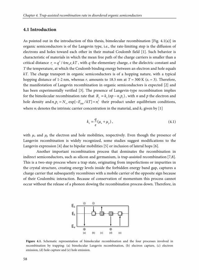
Chapter 4. Trap-assisted recombination rate in disordered organic semiconductors
58
4.1 Introduction As pointed out in the introduction of this thesis, bimolecular recombination [Fig. 4.1(a)] in organic semiconductors is of the Langevin type, i.e., the rate-limiting step is the diffusion of electrons and holes toward each other in their mutual Coulomb field [1]. Such behavior is characteristic of materials in which the mean free path of the charge carriers is smaller than a critical distance kTεπεqr rc 0
2 4/= , with q the elementary charge, ε the dielectric constant and T the temperature, at which the Coulomb binding energy between an electron and hole equals kT. The charge transport in organic semiconductors is of a hopping nature, with a typical hopping distance of 1-2 nm, whereas rc amounts to 18.5 nm at T = 300 K (εr = 3). Therefore, the manifestation of Langevin recombination in organic semiconductors is expected [2] and has been experimentally verified [3]. The presence of Langevin-type recombination implies for the bimolecular recombination rate that )( 11 pnnpkR LL −= , with n and p the electron and hole density and 2
gapcv11 ]/exp[ inkTENpn =−= their product under equilibrium conditions, where ni denotes the intrinsic carrier concentration in the material, and kL given by [1]
)( pnL μμεqk += , (4.1)
with μn and μp the electron and hole mobilities, respectively. Even though the presence of Langevin recombination is widely recognized, some studies suggest modifications to the Langevin expression [4] due to bipolar mobilities [5] or inclusion of lateral hops [6]. Another important recombination process that dominates the recombination in indirect semiconductors, such as silicon and germanium, is trap-assisted recombination [7,8]. This is a two-step process where a trap state, originating from imperfections or impurities in the crystal structure, creating energy levels inside the forbidden energy band gap, captures a charge carrier that subsequently recombines with a mobile carrier of the opposite sign because of their Coulombic interaction. Because of conservation of momentum this process cannot occur without the release of a phonon slowing the recombination process down. Therefore, in
Figure 4.1. Schematic representation of bimolecular recombination and the four processes involved in recombination by trapping: (a) bimolecular Langevin recombination, (b) electron capture, (c) electron emission, (d) hole capture and (e) hole emission.
Ec
E
E
t
v
(a) (b) (c) (d) (e)
--
- -
++
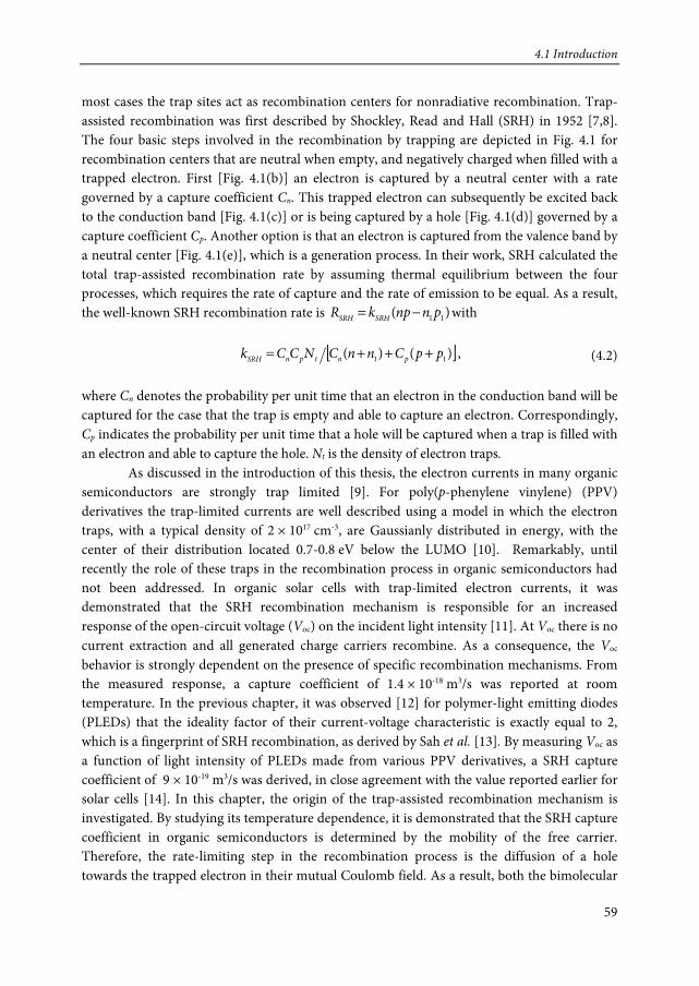
4.1 Introduction
59
most cases the trap sites act as recombination centers for nonradiative recombination. Trap-assisted recombination was first described by Shockley, Read and Hall (SRH) in 1952 [7,8]. The four basic steps involved in the recombination by trapping are depicted in Fig. 4.1 for recombination centers that are neutral when empty, and negatively charged when filled with a trapped electron. First [Fig. 4.1(b)] an electron is captured by a neutral center with a rate governed by a capture coefficient Cn. This trapped electron can subsequently be excited back to the conduction band [Fig. 4.1(c)] or is being captured by a hole [Fig. 4.1(d)] governed by a capture coefficient Cp. Another option is that an electron is captured from the valence band by a neutral center [Fig. 4.1(e)], which is a generation process. In their work, SRH calculated the total trap-assisted recombination rate by assuming thermal equilibrium between the four processes, which requires the rate of capture and the rate of emission to be equal. As a result, the well-known SRH recombination rate is )( 11 pnnpkR SRHSRH −= with [ ])()( 11 ppCnnCNCCk pntpnSRH +++= , (4.2) where Cn denotes the probability per unit time that an electron in the conduction band will be captured for the case that the trap is empty and able to capture an electron. Correspondingly, Cp indicates the probability per unit time that a hole will be captured when a trap is filled with an electron and able to capture the hole. Nt is the density of electron traps. As discussed in the introduction of this thesis, the electron currents in many organic semiconductors are strongly trap limited [9]. For poly(p-phenylene vinylene) (PPV) derivatives the trap-limited currents are well described using a model in which the electron traps, with a typical density of 2 × 1017 cm-3, are Gaussianly distributed in energy, with the center of their distribution located 0.7-0.8 eV below the LUMO [10]. Remarkably, until recently the role of these traps in the recombination process in organic semiconductors had not been addressed. In organic solar cells with trap-limited electron currents, it was demonstrated that the SRH recombination mechanism is responsible for an increased response of the open-circuit voltage (Voc) on the incident light intensity [11]. At Voc there is no current extraction and all generated charge carriers recombine. As a consequence, the Voc behavior is strongly dependent on the presence of specific recombination mechanisms. From the measured response, a capture coefficient of 1.4 × 10⁻¹⁸ m3/s was reported at room temperature. In the previous chapter, it was observed [12] for polymer-light emitting diodes (PLEDs) that the ideality factor of their current-voltage characteristic is exactly equal to 2, which is a fingerprint of SRH recombination, as derived by Sah et al. [13]. By measuring Voc as a function of light intensity of PLEDs made from various PPV derivatives, a SRH capture coefficient of 9 × 10-19 m3/s was derived, in close agreement with the value reported earlier for solar cells [14]. In this chapter, the origin of the trap-assisted recombination mechanism is investigated. By studying its temperature dependence, it is demonstrated that the SRH capture coefficient in organic semiconductors is determined by the mobility of the free carrier. Therefore, the rate-limiting step in the recombination process is the diffusion of a hole towards the trapped electron in their mutual Coulomb field. As a result, both the bimolecular
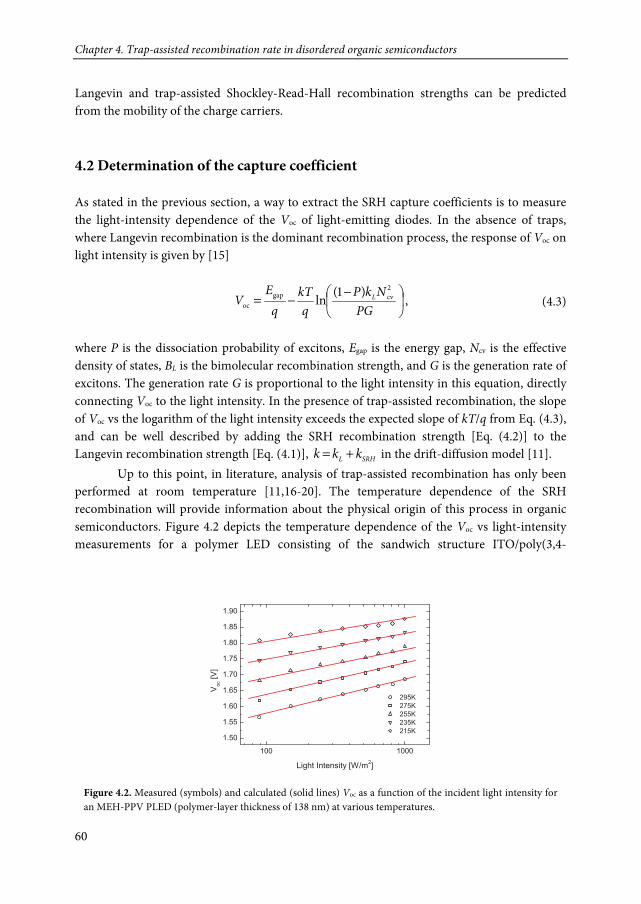
Chapter 4. Trap-assisted recombination rate in disordered organic semiconductors
60
Langevin and trap-assisted Shockley-Read-Hall recombination strengths can be predicted from the mobility of the charge carriers. 4.2 Determination of the capture coefficient As stated in the previous section, a way to extract the SRH capture coefficients is to measure the light-intensity dependence of the Voc of light-emitting diodes. In the absence of traps, where Langevin recombination is the dominant recombination process, the response of Voc on light intensity is given by [15]
−−=PG
NkPq
kTq
EV L
2cvgap
oc)1(ln , (4.3)
where P is the dissociation probability of excitons, Egap is the energy gap, Ncv is the effective density of states, BL is the bimolecular recombination strength, and G is the generation rate of excitons. The generation rate G is proportional to the light intensity in this equation, directly connecting Voc to the light intensity. In the presence of trap-assisted recombination, the slope of Voc vs the logarithm of the light intensity exceeds the expected slope of kT/q from Eq. (4.3), and can be well described by adding the SRH recombination strength [Eq. (4.2)] to the Langevin recombination strength [Eq. (4.1)], SRHL kkk += in the drift-diffusion model [11]. Up to this point, in literature, analysis of trap-assisted recombination has only been performed at room temperature [11,16-20]. The temperature dependence of the SRH recombination will provide information about the physical origin of this process in organic semiconductors. Figure 4.2 depicts the temperature dependence of the Voc vs light-intensity measurements for a polymer LED consisting of the sandwich structure ITO/poly(3,4-
Figure 4.2. Measured (symbols) and calculated (solid lines) Voc as a function of the incident light intensity for an MEH-PPV PLED (polymer-layer thickness of 138 nm) at various temperatures.
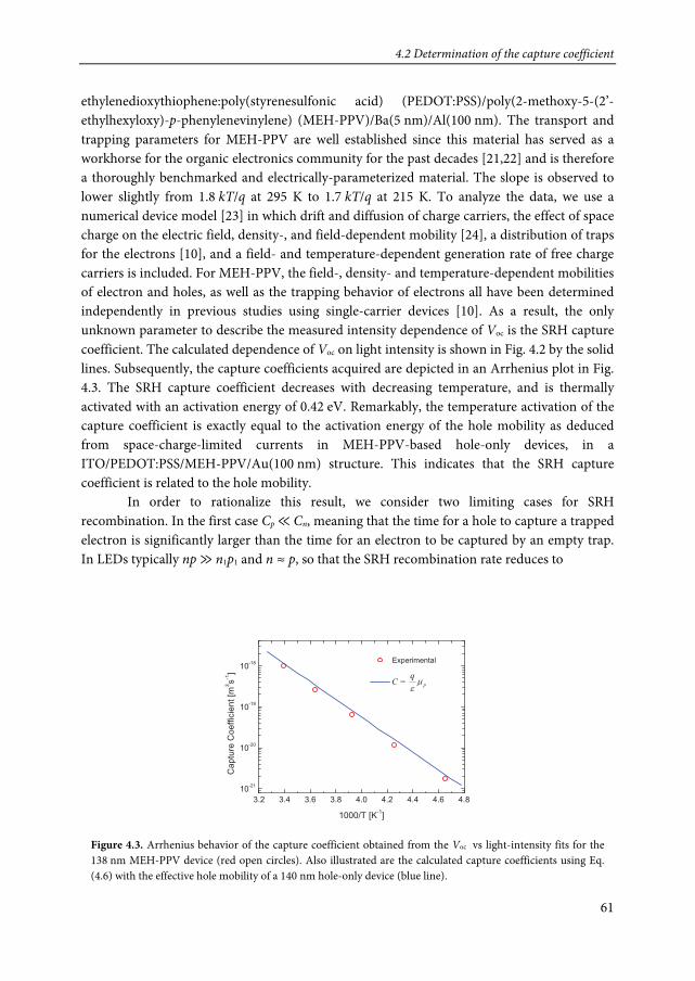
4.2 Determination of the capture coefficient
61
ethylenedioxythiophene:poly(styrenesulfonic acid) (PEDOT:PSS)/poly(2-methoxy-5-(2’-ethylhexyloxy)-p-phenylenevinylene) (MEH-PPV)/Ba(5 nm)/Al(100 nm). The transport and trapping parameters for MEH-PPV are well established since this material has served as a workhorse for the organic electronics community for the past decades [21,22] and is therefore a thoroughly benchmarked and electrically-parameterized material. The slope is observed to lower slightly from 1.8 kT/q at 295 K to 1.7 kT/q at 215 K. To analyze the data, we use a numerical device model [23] in which drift and diffusion of charge carriers, the effect of space charge on the electric field, density-, and field-dependent mobility [24], a distribution of traps for the electrons [10], and a field- and temperature-dependent generation rate of free charge carriers is included. For MEH-PPV, the field-, density- and temperature-dependent mobilities of electron and holes, as well as the trapping behavior of electrons all have been determined independently in previous studies using single-carrier devices [10]. As a result, the only unknown parameter to describe the measured intensity dependence of Voc is the SRH capture coefficient. The calculated dependence of Voc on light intensity is shown in Fig. 4.2 by the solid lines. Subsequently, the capture coefficients acquired are depicted in an Arrhenius plot in Fig. 4.3. The SRH capture coefficient decreases with decreasing temperature, and is thermally activated with an activation energy of 0.42 eV. Remarkably, the temperature activation of the capture coefficient is exactly equal to the activation energy of the hole mobility as deduced from space-charge-limited currents in MEH-PPV-based hole-only devices, in a ITO/PEDOT:PSS/MEH-PPV/Au(100 nm) structure. This indicates that the SRH capture coefficient is related to the hole mobility. In order to rationalize this result, we consider two limiting cases for SRH recombination. In the first case Cp ≪ Cn, meaning that the time for a hole to capture a trapped electron is significantly larger than the time for an electron to be captured by an empty trap. In LEDs typically np ≫ n1p1 and n ≈ p, so that the SRH recombination rate reduces to
Figure 4.3. Arrhenius behavior of the capture coefficient obtained from the Voc vs light-intensity fits for the 138 nm MEH-PPV device (red open circles). Also illustrated are the calculated capture coefficients using Eq. (4.6) with the effective hole mobility of a 140 nm hole-only device (blue line).

Chapter 4. Trap-assisted recombination rate in disordered organic semiconductors
62
pNCR tpSRH = . (4.4) The second case to consider is the opposite of the first, Cp ≫ Cn. For that case, the SRH equation reduces to nNCR tnSRH = . (4.5) Both these equations resemble the equation for bimolecular Langevin recombination
npkR LL = (np ≫ n1p1), with kL replaced by Cn or Cp. In the first case, Cp ≪ Cn, the rate-limiting step is the capture of a trapped electron by a free hole, which involves the process of two oppositely-charged carriers being attracted to each other in their mutual Coulomb field, Figs. 4.1(d) and 4.1(e). This process is similar to bimolecular Langevin recombination, with the only difference that the trapped electron cannot move, meaning that μn = 0. In that case, the SRH recombination coefficient Cp for hole capture by a trapped electron would be
pp μεqC = . (4.6)
In Fig. 4.3 the calculated capture coefficient Cp is plotted as a solid line, using the experimentally determined hole mobility of MEH-PPV. As can be observed in Fig. 4.3, the value of the experimental capture coefficients determined from the intensity dependence of Voc is in very good agreement with the predicted value from Eq. (4.6). This confirms that the SRH recombination in organic semiconductors is determined by diffusion of the free carrier towards the trapped carrier, similar to Langevin recombination where both free carriers diffuse towards each other. 4.3 Radiative trap-assisted recombination In most organic semiconductors, trap-assisted recombination is of a nonradiative nature which denotes SRH recombination as a loss mechanism in LEDs [12,14]. However, for a white-emitting copolymer, where green- and red-emitting chromophores are incorporated in the blue-emitting polyfluorene backbone [25, 26], it has been demonstrated in the previous chapter that the blue part of the emission spectrum arises from Langevin recombination, whereas the red emission originates from SRH recombination of holes with electrons that are trapped on the red chromophore [12]. As a result, both Langevin and SRH can be simultaneously studied by measuring the light output-voltage (L-V) characteristics through selective optical filters. Figure 4.4 depicts the ratio of the red (SRH) and blue (Langevin) emission as a function of voltage for various temperatures. Since the Langevin recombination rate is quadratic in carrier density, whereas the SRH rate is linear, this ratio drops for increasing voltage. More importantly, the ratio is temperature independent. Since the blue-
4.4 Predictive modeling
63
emission rate arises from Langevin recombination, the blue light curve follows the temperature dependence of the highest (hole) mobility in the Langevin expression [Eq. (4.1)]. The trap-assisted red emission on the other hand scales with the capture coefficient Cp [Eq. (4.4)]. The temperature independence of their ratio unambiguously demonstrates that the SRH capture coefficient of the red emission is also dominated by the hole mobility, possessing the same temperature-, field- and density dependence. 4.4 Predictive modeling The understanding of trap-assisted recombination paves the way for a fully predictive description of charge transport and recombination in organic LEDs. From single-carrier devices, the electron and hole mobilities μn(n,E,T) and μp(p,E,T) can be derived, including their dependence on density, electric field and temperature. Furthermore, from electron-only diodes, the number of electron traps Nt can be derived. In a recent study, we demonstrated that at room temperature the inclusion of the measured SRH coefficient in an OLED device model gives a consistent description of the bipolar PLED characteristics without the need for adjusting the Langevin expression [14]. Moreover, now knowing the origin of SRH in organic semiconductors, the modeling of bipolar organic LEDs does not require any additional parameter. The SRH capture coefficient is given by pp μεqC )/(= , so that SRH recombination can be simply approximated by pNTEpμεqR tpSRH ),,()/(= , while Langevin recombination is given by npTEpμTEnμεqR pnL )],,(),,()[/( += . Together with an earlier reported universal Arrhenius relation of the mobility [27], the result described in this chapter for the first time enables full predictive modeling of organic LEDs.
Figure 4.4. Ratio of the red (550 nm longpass filter) and the blue light (blue dichroic filter) of a white light-emitting copolymer as a function of voltage for various temperatures.
Chapter 4. Trap-assisted recombination rate in disordered organic semiconductors
64
4.5 Conclusions In conclusion, we have investigated the mechanism of recombination via trapping, as an addition to bimolecular recombination. The temperature behavior of trap-assisted recombination revealed that the capture coefficient is thermally activated, equal to the activation of the experimental hole mobility. We have demonstrated that the trap-assisted recombination in disordered organic semiconductors is governed by the diffusion of the free carrier (hole) towards the trapped carrier (electron), similar to Langevin recombination for free carriers where both carriers are mobile. As a result, with the charge-carrier mobilities and amount of trapping centers known, the complete recombination process in disordered organic semiconductors can be predicted.
References
65
References
[1] P. Langevin, Ann. Chim. Phys. 28, 433 (1903).
[2] U. Albrecht and H. Bässler, Chem. Phys. 199, 207 (1995).
[3] P. W. M. Blom, M. J. M. de Jong, and S. Breedijk, Appl. Phys. Lett. 71, 930 (1997).
[4] C. Groves and N. C. Greenham, Phys. Rev. B. 78, 155205 (2008).
[5] J. J. M. van der Holst, F. W. A. van Oost, R. Coehoorn, and P. A. Bobbert, Phys. Rev. B 80, 235202 (2009).
[6] S. L. M. van Mensfoort, J. Billen, M. Carvelli, S. I. E. Vulto, R. A. J. Janssen, and R. Coehoorn, J. Appl. Phys. 109, 064502 (2011).
[7] W. Shockley and W. T. Read, Phys. Rev. 87, 835 (1952).
[8] N. Hall, Phys. Rev. 83, 228 (1952); ibid. 87, 387 (1952).
[9] P. W. M. Blom, M. J. M. de Jong, and J. J. M. Vleggaar, Appl. Phys. Lett. 68, 3308 (1996).
[10] H. T. Nicolai, M. M. Mandoc, P. W. M. Blom, Phys. Rev. B. 83, 195204 (2011).
[11] M. M. Mandoc, W. Veurman, L. J. A. Koster, B. De Boer, and P. W. M. Blom, Adv. Funct. Mater. 17, 2167 (2007).
[12] G. A. H. Wetzelaer, M. Kuik, H. T. Nicolai, and P. W. M. Blom, Phys. Rev. B. 83, 165204 (2011).
[13] C. T. Sah, R. N. Noyce, and W. Shockley, Proc. IRE 45, 1228 (1957).
[14] M. Kuik, H. T. Nicolai, M. Lenes, G. A. H. Wetzelaer, M. Lu, and P. W. M. Blom, Appl. Phys. Lett. 98, 093301 (2011).
[15] L. J. A. Koster, V. D. Mihailetchi, R. Ramaker, and P. W. M. Blom, Appl. Phys. Lett. 86, 123509 (2005).
[16] M. M. Mandoc, F. B. Kooistra, J. C. Hummelen, B. de Boer, and P. W. M. Blom, App. Phys. Lett. 91, 263505 (2007).
[17] R. A. Street, M. Schoendorf, A. Roy, and J. H. Lee, Phys. Rev. B. 81, 205307 (2010).
[18] T. Kirchartz, B. E. Pieters, J. Kirkpatrick, U. Rau, and J. Nelson, Phys. Rev. B. 83, 115209 (2011).
Chapter 4. Trap-assisted recombination rate in disordered organic semiconductors
66
[19] L. Tzabari and N. Tessler, J. Appl. Phys. 109, 064501 (2011).
[20] S. R. Cowan, W. L. Leong, N. Banerji, G. Dennler, and A. J. Heeger, Adv. Funct. Mater. 21, 3083 (2011).
[21] D. Braun and A. J. Heeger, Appl. Phys. Lett. 58, 1982 (1991).
[22] G. Yu, J. Gao, J. C. Hummelen, F. Wudl, and A. J. Heeger, Science 270, 5243, 1789 (1995).
[23] L. J. A Koster, E. P. C. Smits, V. D. Mihailetchi, and P. W. M. Blom, Phys. Rev. B 72, 085205 (2005).
[24] W. F. Pasveer, J. Cottaar, C. Tanase, R. Coehoorn, P. A. Bobbert, P. W. M. Blom, D. M. de Leeuw, and M. A. J. Michels, Phys. Rev. Lett. 94, 206601 (2005).
[25] M. de Kok, W. Sarfert, and R. Paetzold, Thin Solid Films 518, 5265 (2010).
[26] M. A. Parshin, J. Ollevier, M. Van der Auweraer, M. M. de Kok, H. T. Nicolai, A. J. Hof, and P. W. M. Blom, J. Appl. Phys. 103, 113711 (2008).
[27] N. I. Craciun, J. Wildeman, and P. W. M. Blom, Phys. Rev. Lett. 100, 056601 (2008).
67
Validity of the Einstein relation in disordered organic semiconductors It is controversial whether energetic disorder in semiconductors is already sufficient
to violate the classical Einstein relation, even in the case of thermal equilibrium. In this chapter, we demonstrate that the Einstein relation is only violated under nonequilibrium conditions due to deeply-trapped carriers, as in diffusion-driven current measurements on organic single-carrier diodes. Removal of these deeply-trapped carriers by recombination unambiguously proves the validity of the Einstein relation in disordered semiconductors in thermal (quasi)equilibrium.
5. Validity of the Einstein relation in disordered organic semiconductors
5
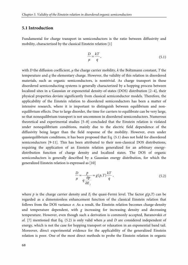
Chapter 5. Validity of the Einstein relation in disordered organic semiconductors
68
5.1 Introduction Fundamental for charge transport in semiconductors is the ratio between diffusivity and mobility, characterized by the classical Einstein relation [1]
qkT
μD = , (5.1)
with D the diffusion coefficient, μ the charge carrier mobility, k the Boltzmann constant, T the temperature and q the elementary charge. However, the validity of this relation in disordered materials, such as organic semiconductors, is nontrivial. As charge transport in these disordered semiconducting systems is generally characterized by a hopping process between localized sites in a Gaussian or exponential density-of-states (DOS) distribution [2–4], their physical properties deviate significantly from classical semiconductor models. Therefore, the applicability of the Einstein relation to disordered semiconductors has been a matter of intensive research, where it is important to distinguish between equilibrium and non-equilibrium effects. Due to large disorder, the time for carriers to equilibrate can be very large, so that nonequilibrium transport is not uncommon in disordered semiconductors. Numerous theoretical and experimental studies [5–8] concluded that the Einstein relation is violated under nonequilibrium conditions, mainly due to the electric field dependence of the diffusivity being larger than the field response of the mobility. However, even under quasiequilibrium conditions, it has been proposed that Eq. (5.1) does not hold for disordered semiconductors [9-11]. This has been attributed to their non-classical DOS distributions, requiring the application of an Einstein relation generalized for an arbitrary energy-distribution function of charge density and localized states. The DOS of organic semiconductors is generally described by a Gaussian energy distribution, for which the generalized Einstein relation is expressed as [10]
qkTTpg
Epq
pμD
f
),(=
∂∂= , (5.2)
where p is the charge carrier density and Ef the quasi-Fermi level. The factor g(p,T) can be regarded as a dimensionless enhancement function of the classical Einstein relation that follows from the DOS variance σ. As a result, the Einstein relation becomes charge-density and temperature dependent, with g increasing for increasing density and decreasing temperature. However, even though such a derivation is commonly accepted, Baranovskii et al. [7] mentioned that Eq. (5.2) is only valid when μ and D are considered independent of energy, which is not the case for hopping transport or relaxation in an exponential band tail. Moreover, direct experimental evidence for the applicability of the generalized Einstein relation is poor. One of the most direct methods to probe the Einstein relation in organic
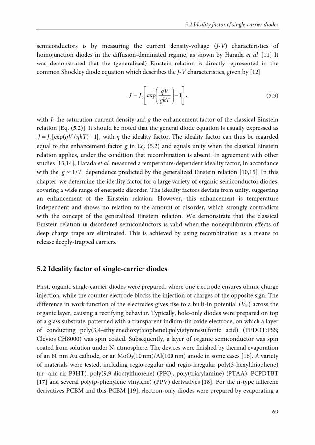
5.2 Ideality factor of single-carrier diodes
69
semiconductors is by measuring the current density-voltage (J-V) characteristics of homojunction diodes in the diffusion-dominated regime, as shown by Harada et al. [11] It was demonstrated that the (generalized) Einstein relation is directly represented in the common Shockley diode equation which describes the J-V characteristics, given by [12]
−
= 1exp0 gkT
qVJJ , (5.3)
with J0 the saturation current density and g the enhancement factor of the classical Einstein relation [Eq. (5.2)]. It should be noted that the general diode equation is usually expressed as
]1)/[exp(0 −= kTηqVJJ , with η the ideality factor. The ideality factor can thus be regarded equal to the enhancement factor g in Eq. (5.2) and equals unity when the classical Einstein relation applies, under the condition that recombination is absent. In agreement with other studies [13,14], Harada et al. measured a temperature-dependent ideality factor, in accordance with the Tg /1∝ dependence predicted by the generalized Einstein relation [10,15]. In this chapter, we determine the ideality factor for a large variety of organic semiconductor diodes, covering a wide range of energetic disorder. The ideality factors deviate from unity, suggesting an enhancement of the Einstein relation. However, this enhancement is temperature independent and shows no relation to the amount of disorder, which strongly contradicts with the concept of the generalized Einstein relation. We demonstrate that the classical Einstein relation in disordered semiconductors is valid when the nonequilibrium effects of deep charge traps are eliminated. This is achieved by using recombination as a means to release deeply-trapped carriers. 5.2 Ideality factor of single-carrier diodes First, organic single-carrier diodes were prepared, where one electrode ensures ohmic charge injection, while the counter electrode blocks the injection of charges of the opposite sign. The difference in work function of the electrodes gives rise to a built-in potential (Vbi) across the organic layer, causing a rectifying behavior. Typically, hole-only diodes were prepared on top of a glass substrate, patterned with a transparent indium-tin oxide electrode, on which a layer of conducting poly(3,4-ethylenedioxythiophene):poly(styrenesulfonic acid) (PEDOT:PSS; Clevios CH8000) was spin coated. Subsequently, a layer of organic semiconductor was spin coated from solution under N2 atmosphere. The devices were finished by thermal evaporation of an 80 nm Au cathode, or an MoO3(10 nm)/Al(100 nm) anode in some cases [16]. A variety of materials were tested, including regio-regular and regio-irregular poly(3-hexylthiophene) (rr- and rir-P3HT), poly(9,9-dioctylfluorene) (PFO), poly(triarylamine) (PTAA), PCPDTBT [17] and several poly(p-phenylene vinylene) (PPV) derivatives [18]. For the n-type fullerene derivatives PCBM and tbis-PCBM [19], electron-only diodes were prepared by evaporating a
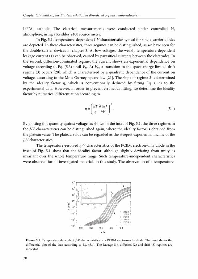
Chapter 5. Validity of the Einstein relation in disordered organic semiconductors
70
LiF/Al cathode. The electrical measurements were conducted under controlled N2 atmosphere, using a Keithley 2400 source meter.
In Fig. 5.1, temperature-dependent J-V characteristics typical for single-carrier diodes are depicted. In these characteristics, three regimes can be distinguished, as we have seen for the double-carrier devices in chapter 3. At low voltages, the weakly temperature-dependent leakage current (1) can be observed, caused by parasitical currents between the electrodes. In the second, diffusion-dominated regime, the current shows an exponential dependence on voltage according to Eq. (5.3) until Vbi. At Vbi, a transition to the space-charge-limited drift regime (3) occurs [20], which is characterized by a quadratic dependence of the current on voltage, according to the Mott-Gurney square law [21]. The slope of regime 2 is determined by the ideality factor η, which is conventionally deduced by fitting Eq. (5.3) to the experimental data. However, in order to prevent erroneous fitting, we determine the ideality factor by numerical differentiation according to
1
ln−
∂
∂=V
Jq
kTη . (5.4)
By plotting this quantity against voltage, as shown in the inset of Fig. 5.1, the three regimes in the J-V characteristics can be distinguished again, where the ideality factor is obtained from the plateau value. The plateau value can be regarded as the steepest exponential incline of the J-V characteristics.
The temperature-resolved η-V characteristics of the PCBM electron-only diode in the inset of Fig. 5.1 show that the ideality factor, although slightly deviating from unity, is invariant over the whole temperature range. Such temperature-independent characteristics were observed for all investigated materials in this study. The observation of a temperature-
Figure 5.1. Temperature dependent J-V characteristics of a PCBM electron-only diode. The inset shows the differential plot of the data according to Eq. (5.4). The leakage (1), diffusion (2) and drift (3) regimes are indicated.
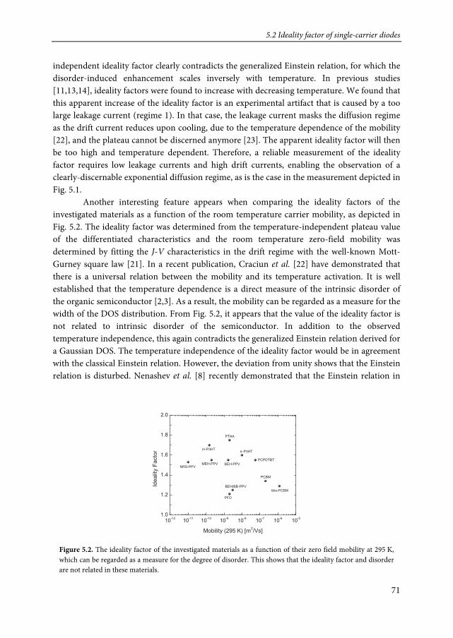
5.2 Ideality factor of single-carrier diodes
71
independent ideality factor clearly contradicts the generalized Einstein relation, for which the disorder-induced enhancement scales inversely with temperature. In previous studies [11,13,14], ideality factors were found to increase with decreasing temperature. We found that this apparent increase of the ideality factor is an experimental artifact that is caused by a too large leakage current (regime 1). In that case, the leakage current masks the diffusion regime as the drift current reduces upon cooling, due to the temperature dependence of the mobility [22], and the plateau cannot be discerned anymore [23]. The apparent ideality factor will then be too high and temperature dependent. Therefore, a reliable measurement of the ideality factor requires low leakage currents and high drift currents, enabling the observation of a clearly-discernable exponential diffusion regime, as is the case in the measurement depicted in Fig. 5.1.
Another interesting feature appears when comparing the ideality factors of the investigated materials as a function of the room temperature carrier mobility, as depicted in Fig. 5.2. The ideality factor was determined from the temperature-independent plateau value of the differentiated characteristics and the room temperature zero-field mobility was determined by fitting the J-V characteristics in the drift regime with the well-known Mott-Gurney square law [21]. In a recent publication, Craciun et al. [22] have demonstrated that there is a universal relation between the mobility and its temperature activation. It is well established that the temperature dependence is a direct measure of the intrinsic disorder of the organic semiconductor [2,3]. As a result, the mobility can be regarded as a measure for the width of the DOS distribution. From Fig. 5.2, it appears that the value of the ideality factor is not related to intrinsic disorder of the semiconductor. In addition to the observed temperature independence, this again contradicts the generalized Einstein relation derived for a Gaussian DOS. The temperature independence of the ideality factor would be in agreement with the classical Einstein relation. However, the deviation from unity shows that the Einstein relation is disturbed. Nenashev et al. [8] recently demonstrated that the Einstein relation in
Figure 5.2. The ideality factor of the investigated materials as a function of their zero field mobility at 295 K, which can be regarded as a measure for the degree of disorder. This shows that the ideality factor and disorder are not related in these materials.
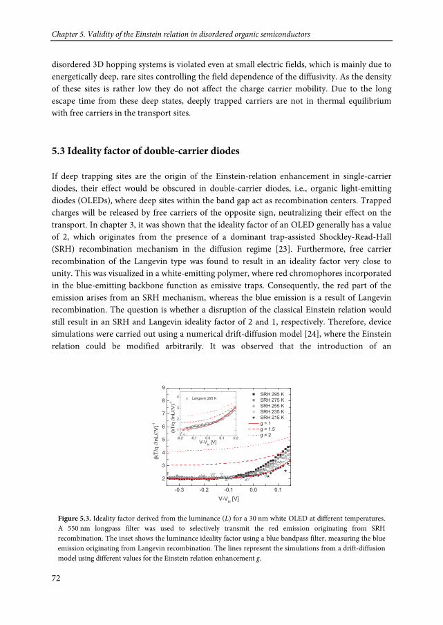
Chapter 5. Validity of the Einstein relation in disordered organic semiconductors
72
disordered 3D hopping systems is violated even at small electric fields, which is mainly due to energetically deep, rare sites controlling the field dependence of the diffusivity. As the density of these sites is rather low they do not affect the charge carrier mobility. Due to the long escape time from these deep states, deeply trapped carriers are not in thermal equilibrium with free carriers in the transport sites. 5.3 Ideality factor of double-carrier diodes If deep trapping sites are the origin of the Einstein-relation enhancement in single-carrier diodes, their effect would be obscured in double-carrier diodes, i.e., organic light-emitting diodes (OLEDs), where deep sites within the band gap act as recombination centers. Trapped charges will be released by free carriers of the opposite sign, neutralizing their effect on the transport. In chapter 3, it was shown that the ideality factor of an OLED generally has a value of 2, which originates from the presence of a dominant trap-assisted Shockley-Read-Hall (SRH) recombination mechanism in the diffusion regime [23]. Furthermore, free carrier recombination of the Langevin type was found to result in an ideality factor very close to unity. This was visualized in a white-emitting polymer, where red chromophores incorporated in the blue-emitting backbone function as emissive traps. Consequently, the red part of the emission arises from an SRH mechanism, whereas the blue emission is a result of Langevin recombination. The question is whether a disruption of the classical Einstein relation would still result in an SRH and Langevin ideality factor of 2 and 1, respectively. Therefore, device simulations were carried out using a numerical drift-diffusion model [24], where the Einstein relation could be modified arbitrarily. It was observed that the introduction of an
Figure 5.3. Ideality factor derived from the luminance (L) for a 30 nm white OLED at different temperatures. A 550 nm longpass filter was used to selectively transmit the red emission originating from SRH recombination. The inset shows the luminance ideality factor using a blue bandpass filter, measuring the blue emission originating from Langevin recombination. The lines represent the simulations from a drift-diffusion model using different values for the Einstein relation enhancement g.
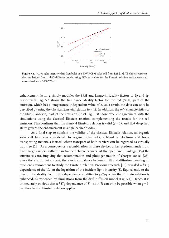
5.3 Ideality factor of double-carrier diodes
73
enhancement factor g simply modifies the SRH and Langevin ideality factors to 2g and 1g, respectively. Fig. 5.3 shows the luminance ideality factor for the red (SRH) part of the emission, which has a temperature-independent value of 2. As a result, the data can only be described by using the classical Einstein relation (g = 1). In addition, the η-V characteristics of the blue (Langevin) part of the emission (inset Fig. 5.3) show excellent agreement with the simulations using the classical Einstein relation, complementing the results for the red emission. This confirms that the classical Einstein relation is valid (g = 1), and that deep trap states govern the enhancement in single-carrier diodes.
As a final step to confirm the validity of the classical Einstein relation, an organic solar cell has been considered. In organic solar cells, a blend of electron- and hole-transporting materials is used, where transport of both carriers can be regarded as virtually trap free [24]. As a consequence, recombination in these devices arises predominantly from free charge carriers, rather than trapped charge carriers. At the open-circuit voltage (Voc) the current is zero, implying that recombination and photogeneration of charges cancel [25]. Since there is no net current, there exists a balance between drift and diffusion, creating an excellent environment to study the Einstein relation. Previous research [13] revealed a kT/q dependence of the Voc on the logarithm of the incident light-intensity (I). Equivalently to the case of the ideality factor, this dependence modifies to gkT/q when the Einstein relation is enhanced, as evidenced by simulations from the drift-diffusion model (Fig. 5.4). Hence, it is immediately obvious that a kT/q dependence of Voc vs ln(I) can only be possible when g = 1, i.e., the classical Einstein relation applies.
Figure 5.4. Voc vs light-intensity data (symbols) of a PPV:PCBM solar cell from Ref. [13]. The lines represent the simulations from a drift-diffusion model using different values for the Einstein relation enhancement g, normalized at I = 2000 W/m2.
Chapter 5. Validity of the Einstein relation in disordered organic semiconductors
74
5.3 Conclusions In conclusion, the validity of the Einstein relation in disordered organic semiconductors has been investigated by studying the diffusion-driven currents of single-carrier diodes. In contrast to earlier reports, a temperature-independent ideality factor was found for both n- and p-type conduction, which is in contradiction with the generalized Einstein relation derived for a Gaussian DOS. Furthermore, the ideality factor was observed to be independent of energetic disorder and its deviation from unity was explained by the presence of energetically deep states within the band gap. The validity of the classical Einstein relation in disordered organic semiconductors was demonstrated in double-carrier devices as OLEDs and solar cells, where these traps are discharged by charge recombination.
References
75
References
[1] A. Einstein, Ann. Phys. 322, 549 (1905).
[2] H. Bässler, Phys. Status Solidi B 175, 15 (1993).
[3] S. V. Novikov, D. H. Dunlap, V. M. Kenkre, P. E. Parris, and A. V. Vannikov, Phys. Rev. Lett. 81, 4472 (1998).
[4] M. C. J. M. Vissenberg and M. Matters, Phys. Rev. B 57, 12964 (1998).
[5] R. Richert, L. Pautmeier, and H. Bässler, Phys. Rev. Lett. 63, 547 (1989).
[6] P. M. Borsenberger, L. Pautmeier, R. Richert, and H. Bässler, J. Chem. Phys. 94, 8276 (1991).
[7] S. D. Baranovskii, T. Faber, F. Hensel, P. Thomas, and G. J. Adriaenssens, J. Non-Cryst. Solids 198-200, 214 (1996).
[8] A. V. Nenashev, F. Jansson, S. D. Baranovskii, R. Österbacka, A. V. Dvurechenskii, and F. Gebhard, Phys. Rev. B 81, 115204 (2010), and references therein.
[9] D. Ritter, E. Zeldov, and K. Weiser, Phys. Rev. B 38, 8296 (1988).
[10] Y. Roichman and N. Tessler, Appl. Phys. Lett. 80, 1948 (2002).
[11] K. Harada, A. G. Werner, M. Pfeiffer, C. J. Bloom, C. M. Elliott, and K. Leo, Phys. Rev. Lett. 94, 036601 (2005).
[12] W. Shockley, Bell Syst. Tech. J. 28, 435 (1949).
[13] L. J. A. Koster, V. D. Mihailetchi, R. Ramaker, and P. W. M. Blom, Appl. Phys. Lett. 86, 123509 (2005).
[14] K. Harada, M. Riede, K. Leo, O. R. Hild, and C. M. Elliott, Phys. Rev. B 77, 195212 (2008).
[15] N. Tessler and Y. Roichman, Org. Electron. 6, 200 (2005).
[16] H. T. Nicolai, G. A. H. Wetzelaer, M. Kuik, A. J. Kronemeijer, B. de Boer, and P. W. M. Blom, Appl. Phys. Lett. 96, 172107 (2010).
[17] M. Lenes, M. Morana, C. J. Brabec, and P. W. M. Blom, Adv. Funct. Mater. 19, 1106 (2009).
[18] C. Tanase, J. Wildeman, and P. W. M. Blom, Adv. Funct. Mater. 15, 2011 (2005).
Chapter 5. Validity of the Einstein relation in disordered organic semiconductors
76
[19] R. K. M. Bouwer, J. C. Hummelen, Chem. Eur. J. 16, 11250 (2010).
[20] P. W. M. Blom, M. J. M. de Jong, and J. J. M. Vleggaar, Appl. Phys. Lett. 68, 3308 (1996).
[21] N. F. Mott and R. W. Gurney, Electronic Processes in Ionic Crystals, (Oxford University Press, London, 1940).
[22] N. I. Craciun, J. Wildeman, and P. W. M. Blom, Phys. Rev. Lett. 100, 056601 (2008).
[23] G. A. H. Wetzelaer, M. Kuik, H. T. Nicolai, P. W. M. Blom, Phys. Rev. B 83, 165204 (2011).
[24] L. J. A. Koster, E. C. P. Smits, V. D. Mihailetchi, and P. W. M. Blom, Phys. Rev. B 72, 085205 (2005).
[25] A. Maurano, R. Hamilton, C. G. Shuttle, A. M. Ballantyne, J. Nelson, B. O’Regan, W. Zhang, I. McCulloch, H. Azimi, M. Morana, C. J. Brabec, and J. R. Durrant, Adv. Mater. 22, 4987 (2010).

77
Origin of the dark-current ideality factor in polymer:fullerene bulk-heterojunction solar cells In organic bulk-heterojunction solar cells, a deviation of the ideality factor of the
dark current from unity is commonly put forward as evidence for the presence of trap-assisted recombination. In this chapter, we demonstrate that the non-ideality of the dark characteristics is determined by deeply-trapped carriers in the transport-dominating constituent of the donor:acceptor blend, rather than a trap-assisted recombination mechanism. The light-intensity dependence of the open-circuit voltage confirms the absence of trap-assisted recombination and demonstrates that the dominant recombination mechanism in the investigated polymer:fullerene solar cells is bimolecular.
6. Origin of the dark-current ideality factor in polymer:fullerene bulk-heterojunction solar cells
6
Chapter 6. Origin of the dark-current ideality factor in polymer:fullerene bulk-heterojunction solar cells
78
6.1 Introduction Since the discovery of organic-semiconductor solar cells comprising a phase-separated blend of a conjugated donor and acceptor material [1], great effort has been put in understanding the physics behind their operation [2]. Particularly, the mechanisms governing charge transport and recombination have received considerable attention. For a conventional (Si) p-n junction solar cell the dark current density is given by
−
= 1exp0D kTη
qVJJ , (6.1)
where J0 is the (reverse bias) saturation current density, V the applied voltage, q the elementary charge, k Boltzmann’s constant, T temperature, and η the ideality factor. The ideality factor determines the slope of the exponential regime of the dark J-V characteristics on a semilogarithmic plot and can be expressed as
1
ln−
∂
∂=V
Jq
kTη . (6.2)
The current density under illumination is given by JL = JD – Jph, where Jph is the photogenerated current density. Subsequently, the open-circuit voltage is given by (JL = 0) )1/ln()/( 0phoc += JJqkTηV . (6.3)
As is the case for organic light-emitting diodes, the ideality factor contains important information on the transport and recombination processes in organic solar cells. It is evident from Eqs. (6.1) and (6.3) that the ideality factor can be independently determined from the slope of the exponential regime of dark J-V characteristics on a semilogarithmic plot [Eq. (6.1)] or by measuring the slope of the dependence of Voc on the logarithm of the light intensity, that scales linearly with Jph [Eq. (6.3)]. For an ideal p-n junction diode without trapping of charge carriers and where recombination is absent or governed by bimolecular recombination, the ideality factor is expected to be equal to unity. However, already in 1957, Sah et al. [3] showed that the ideality factor of a classical p-n junction is calculated to increase due to trap-assisted recombination in the space-charge region. In their calculations, electrons immobilized in trapping sites recombine with free holes as described by the Shockley-Read-Hall (SRH) formalism [4,5]. Their predicted enhancement of the ideality factor, reaching a value of 2 for fully trap-assisted recombination, has also recently been found in organic light-emitting diodes [6,7], as described in chapter 3. From dark-current measurements on polymer:fullerene organic solar cells, ideality factors of typically 1.3-2.0 have been reported [8-11]. Furthermore, it was first demonstrated by Mandoc et al. [12,13] that the presence of trap-
6.2 Ideality factor of organic solar cells in dark and under illumination
79
assisted recombination in organic solar cells can, as implied by Eq. (6.3), be visualized by measuring the open-circuit voltage (Voc) of an organic solar cell as a function of the incident light intensity. In these experiments on all-polymer solar cells [13], also a deviation of η from unity was observed due to trap-assisted recombination. This result seems to be consistent with the observation of η larger than unity in dark-current measurements. As a consequence, an ideality factor greater than unity is often used as evidence for a dominant trap-assisted recombination process in organic solar cells [8-10].
However, it appears that an unresolved discrepancy exists between the dark ideality factor and the light-intensity dependence of Voc, which should have equal values according to Eqs. (6.1) and (6.3). A dark ideality factor larger than unity is often measured for organic solar cells of which both electron and hole transport are demonstrated to be trap free, which is in contradiction with the appearance of trap-assisted recombination to explain the ideality factor. Furthermore, Voc vs light-intensity measurements also showing a deviation from unity [13] were carried out on all-polymer solar cells of which the electron transport was observed to be clearly trap limited. On the other hand, solar cells with trap-free transport indeed do show an ideality factor of unity when Voc vs light intensity is measured, whereas in the dark current still a deviation from unity is found [11]. Attributing the occurrence of a dark ideality factor larger than unity to trap-assisted recombination is therefore highly questionable. Cowan et al. [10] recently argued that the higher density of charge carriers under illumination could impose a crossover from trap-assisted to bimolecular recombination, due to a difference in density dependence of these recombination mechanisms [6,7]. This would lead to a lower ideality factor under illumination as compared to the dark ideality factor. In this chapter, we demonstrate that in organic solar cells with trap-free transport, the dark ideality factor is determined by the transport-dominating carrier in the blend, whereas the ideality factor under illumination is solely governed by bimolecular recombination. 6.2 Ideality factor of organic solar cells in dark and under illumination Organic bulk-heterojunction solar cells were fabricated using the well-studied donor materials poly[2,6-(4,4-bis-(2-ethylhexyl)-4H-cyclopenta[2,1-b;3,4-b’]-dithiophene)-alt-4,7-(2,1,3-benzothiadiazole)] (PCPDTBT), poly[2-methoxy-5-(2’-ethylhexyloxy)-p-phenylenevinylene] (MEH-PPV) and poly[9,9-didecanefluorene-alt-(bis-thienylene) benzothiadiazole] (PF10TBT), blended with the fullerene derivative [6,6]-phenyl-C61-butyric acid methyl ester (PCBM) as acceptor material in a 1:4 weight ratio. Photoactive layers were prepared by spin casting the chlorobenzene solutions under nitrogen atmosphere on clean glass substrates, prepatterned with indium tin oxide and coated with a 60 nm film of poly(3,4-ethylenedioxythiophene):poly(styrenesulfonic acid) (VP AI4083, H.C. Starck). The devices were finished by thermal evaporation of a LiF(1 nm)/Al(100 nm) cathode. Electrical measurements were conducted in a controlled N2 atmosphere in dark and under illumination
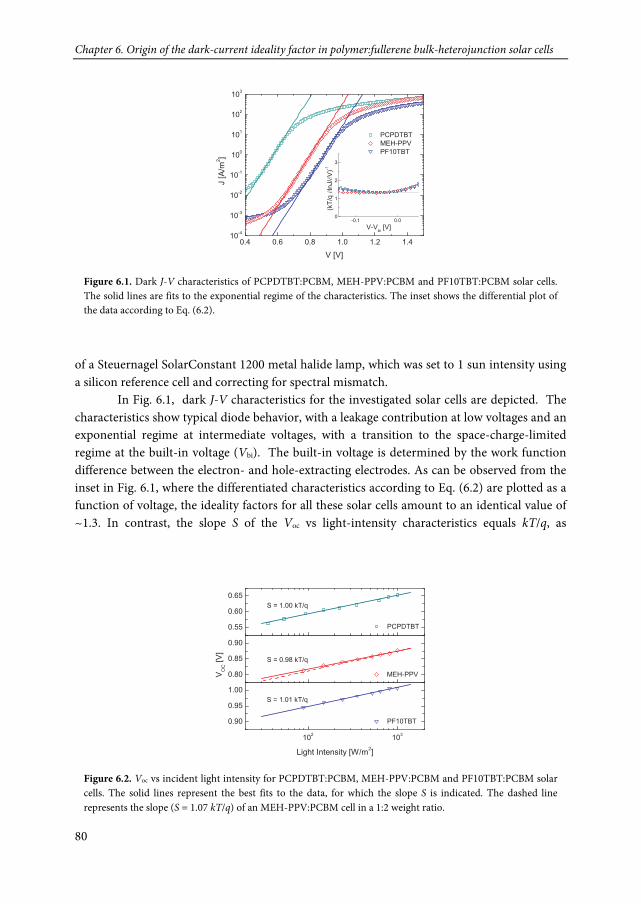
Chapter 6. Origin of the dark-current ideality factor in polymer:fullerene bulk-heterojunction solar cells
80
of a Steuernagel SolarConstant 1200 metal halide lamp, which was set to 1 sun intensity using a silicon reference cell and correcting for spectral mismatch.
In Fig. 6.1, dark J-V characteristics for the investigated solar cells are depicted. The characteristics show typical diode behavior, with a leakage contribution at low voltages and an exponential regime at intermediate voltages, with a transition to the space-charge-limited regime at the built-in voltage (Vbi). The built-in voltage is determined by the work function difference between the electron- and hole-extracting electrodes. As can be observed from the inset in Fig. 6.1, where the differentiated characteristics according to Eq. (6.2) are plotted as a function of voltage, the ideality factors for all these solar cells amount to an identical value of ~1.3. In contrast, the slope S of the Voc vs light-intensity characteristics equals kT/q, as
Figure 6.1. Dark J-V characteristics of PCPDTBT:PCBM, MEH-PPV:PCBM and PF10TBT:PCBM solar cells. The solid lines are fits to the exponential regime of the characteristics. The inset shows the differential plot of the data according to Eq. (6.2).
Figure 6.2. Voc vs incident light intensity for PCPDTBT:PCBM, MEH-PPV:PCBM and PF10TBT:PCBM solar cells. The solid lines represent the best fits to the data, for which the slope S is indicated. The dashed line represents the slope (S = 1.07 kT/q) of an MEH-PPV:PCBM cell in a 1:2 weight ratio.
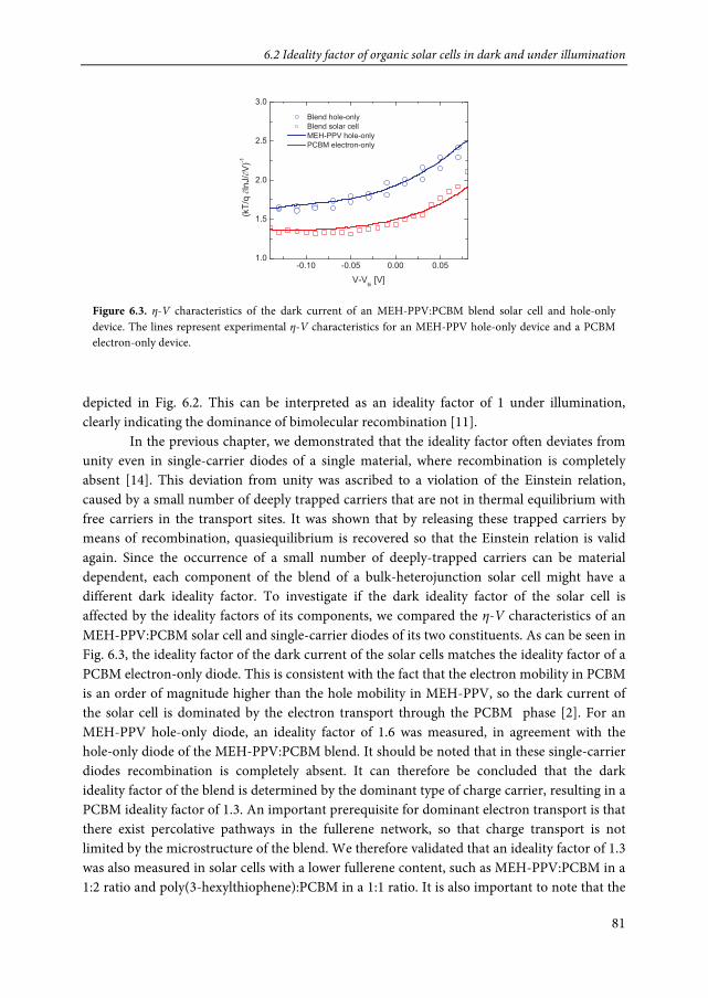
6.2 Ideality factor of organic solar cells in dark and under illumination
81
depicted in Fig. 6.2. This can be interpreted as an ideality factor of 1 under illumination, clearly indicating the dominance of bimolecular recombination [11].
In the previous chapter, we demonstrated that the ideality factor often deviates from unity even in single-carrier diodes of a single material, where recombination is completely absent [14]. This deviation from unity was ascribed to a violation of the Einstein relation, caused by a small number of deeply trapped carriers that are not in thermal equilibrium with free carriers in the transport sites. It was shown that by releasing these trapped carriers by means of recombination, quasiequilibrium is recovered so that the Einstein relation is valid again. Since the occurrence of a small number of deeply-trapped carriers can be material dependent, each component of the blend of a bulk-heterojunction solar cell might have a different dark ideality factor. To investigate if the dark ideality factor of the solar cell is affected by the ideality factors of its components, we compared the η-V characteristics of an MEH-PPV:PCBM solar cell and single-carrier diodes of its two constituents. As can be seen in Fig. 6.3, the ideality factor of the dark current of the solar cells matches the ideality factor of a PCBM electron-only diode. This is consistent with the fact that the electron mobility in PCBM is an order of magnitude higher than the hole mobility in MEH-PPV, so the dark current of the solar cell is dominated by the electron transport through the PCBM phase [2]. For an MEH-PPV hole-only diode, an ideality factor of 1.6 was measured, in agreement with the hole-only diode of the MEH-PPV:PCBM blend. It should be noted that in these single-carrier diodes recombination is completely absent. It can therefore be concluded that the dark ideality factor of the blend is determined by the dominant type of charge carrier, resulting in a PCBM ideality factor of 1.3. An important prerequisite for dominant electron transport is that there exist percolative pathways in the fullerene network, so that charge transport is not limited by the microstructure of the blend. We therefore validated that an ideality factor of 1.3 was also measured in solar cells with a lower fullerene content, such as MEH-PPV:PCBM in a 1:2 ratio and poly(3-hexylthiophene):PCBM in a 1:1 ratio. It is also important to note that the
Figure 6.3. η-V characteristics of the dark current of an MEH-PPV:PCBM blend solar cell and hole-only device. The lines represent experimental η-V characteristics for an MEH-PPV hole-only device and a PCBM electron-only device.
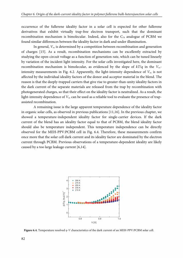
Chapter 6. Origin of the dark-current ideality factor in polymer:fullerene bulk-heterojunction solar cells
82
occurrence of the fullerene ideality factor in a solar cell is expected for other fullerene derivatives that exhibit virtually trap-free electron transport, such that the dominant recombination mechanism is bimolecular. Indeed, also for the C70 analogue of PCBM we found similar differences between the ideality factor in dark and under illumination.
In general, Voc is determined by a competition between recombination and generation of charges [15]. As a result, recombination mechanisms can be excellently extracted by studying the open-circuit voltage as a function of generation rate, which can be tuned linearly by variation of the incident light intensity. For the solar cells investigated here, the dominant recombination mechanism is bimolecular, as evidenced by the slope of kT/q in the Voc-intensity measurements in Fig. 6.2. Apparently, the light-intensity dependence of Voc is not affected by the individual ideality factors of the donor and acceptor material in the blend. The reason is that the deeply-trapped carriers that give rise to greater-than-unity ideality factors in the dark current of the separate materials are released from the trap by recombination with photogenerated charges, so that their effect on the ideality factor is neutralized. As a result, the light-intensity dependence of Voc can be used as a reliable tool to evaluate the presence of trap-assisted recombination.
A remaining issue is the large apparent temperature dependence of the ideality factor in organic solar cells, as observed in previous publications [11,16]. In the previous chapter, we showed a temperature-independent ideality factor for single-carrier devices. If the dark current of the blend has an ideality factor equal to that of PCBM, the blend ideality factor should also be temperature independent. This temperature independence can be directly observed for the MEH-PPV:PCBM cell in Fig. 6.4. Therefore, these measurements confirm once more that the solar cell dark current and its ideality factor are dominated by the electron current through PCBM. Previous observations of a temperature-dependent ideality are likely caused by a too large leakage current [6,14].
Figure 6.4. Temperature resolved η-V characteristics of the dark current of an MEH-PPV:PCBM solar cell.
6.3 Conclusions
83
6.3 Conclusions In conclusion, we have demonstrated that the ideality factor of the dark current of organic bulk-heterojunction solar cells is dominated by the fastest-transporting material in the blend. The non-ideality is caused by deeply trapped carriers, of which the effect is neutralized under illumination, so that the ideality factor under illumination is a reliable indication of the recombination mechanism taking place. Consequently, a dark ideality factor deviating from unity cannot be used as an indication for the presence of trap-assisted recombination in an organic solar cell.
Chapter 6. Origin of the dark-current ideality factor in polymer:fullerene bulk-heterojunction solar cells
84
References
[1] G. Yu, J. Gao, J. C. Hummelen, F. Wudl, and A. J. Heeger, Science 270, 1789 (1995).
[2] P. W. M. Blom, V. D. Mihailetchi, L. J. A. Koster, and D. E. Markov, Adv. Mater. 19, 1551 (2007).
[3] C. T. Sah, R. N. Noyce, and W. Shockley, Proc. IRE 45, 1228 (1957).
[4] W. Shockley and W. T. Read, Phys. Rev. 87, 835 (1952).
[5] R. N. Hall, Phys. Rev. 83, 228 (1951); ibid. 87, 387 (1952).
[6] G. A. H. Wetzelaer, M. Kuik, H. T. Nicolai, and P. W. M. Blom, Phys. Rev. B 83, 165204 (2011).
[7] M. Kuik, H. T. Nicolai, M. Lenes, G. A. H. Wetzelaer, M. Lu, and P. W. M. Blom, Appl. Phys. Lett. 98, 093301 (2011).
[8] R. A. Street, M. Schoendorf, A. Roy, and J. H. Lee, Phys. Rev. B 81, 205307 (2010).
[9] T. Kirchartz, B. E. Pieters, J. Kirkpatrick, U. Rau, and J. Nelson, Phys. Rev. B 83, 115209 (2011).
[10] S. R. Cowan, W. L. Leong, N. Banerji, G. Dennler, and A. J. Heeger, Adv. Funct. Mater. 21, 3083 (2011).
[11] L. J. A. Koster, V. D. Mihailetchi, R. Ramaker, and P. W. M. Blom, Appl. Phys. Lett. 86, 123509 (2005).
[12] M. M. Mandoc, F. B. Kooistra, J. C. Hummelen, B. de Boer and P. W. M. Blom, Appl. Phys. Lett. 91, 263505 (2007).
[13] M. M. Mandoc, W. Veurman, L. J. A. Koster, B. de Boer, and P. W. M. Blom, Adv. Funct. Mater. 17, 2167 (2007).
[14] G. A. H. Wetzelaer, L. J. A. Koster, and P. W. M. Blom, Phys. Rev. Lett. 107, 066605 (2011).
[15] A. Maurano, R. Hamilton, C. G. Shuttle, A. M. Ballantyne, J. Nelson, B. O’Regan, W. Zhang, I. McCulloch, H. Azimi, M. Morana, C. J. Brabec, and J. R. Durrant, Adv. Mater. 22, 4987 (2010).
[16] I. Riedel, E. von Hauff, J. Parisi, N. Martín, F. Giacalone, V. Dyakonov, Adv. Funct. Mater. 15, 1979 (2005).

85
Quantifying bimolecular recombination in organic solar cells in steady state In this chapter, a steady-state method to probe bimolecular recombination in
organic solar cells is presented. The technique is applicable to thin-film solar cells at any temperature and does not require a separate measurement setup other than conventional solar-cell testing equipment. The key element is the derivation of a simple analytical expression that directly gives access to the recombination strength by employing the concept of charge neutralization, a process that is competing with charge recombination. The analytical equation requires only standard transport parameters as input. We demonstrate the suitability of our technique by applying it to polymer:fullerene solar cells.
7. Quantifying bimolecular recombination in organic solar cells in steady state
7
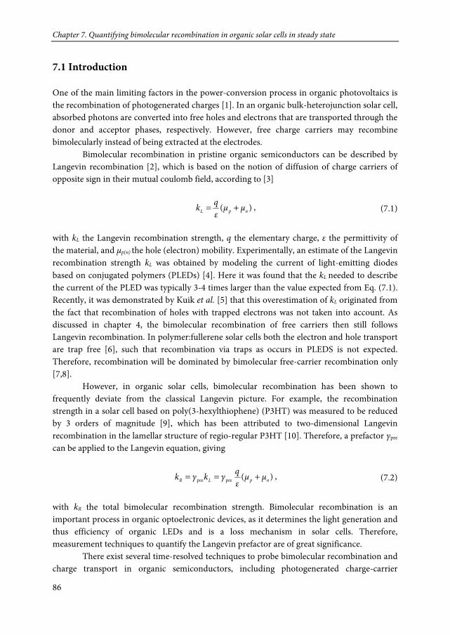
Chapter 7. Quantifying bimolecular recombination in organic solar cells in steady state
86
7.1 Introduction One of the main limiting factors in the power-conversion process in organic photovoltaics is the recombination of photogenerated charges [1]. In an organic bulk-heterojunction solar cell, absorbed photons are converted into free holes and electrons that are transported through the donor and acceptor phases, respectively. However, free charge carriers may recombine bimolecularly instead of being extracted at the electrodes.
Bimolecular recombination in pristine organic semiconductors can be described by Langevin recombination [2], which is based on the notion of diffusion of charge carriers of opposite sign in their mutual coulomb field, according to [3]
)( npL μμεqk += , (7.1)
with kL the Langevin recombination strength, q the elementary charge, ε the permittivity of the material, and μp(n) the hole (electron) mobility. Experimentally, an estimate of the Langevin recombination strength kL was obtained by modeling the current of light-emitting diodes based on conjugated polymers (PLEDs) [4]. Here it was found that the kL needed to describe the current of the PLED was typically 3-4 times larger than the value expected from Eq. (7.1). Recently, it was demonstrated by Kuik et al. [5] that this overestimation of kL originated from the fact that recombination of holes with trapped electrons was not taken into account. As discussed in chapter 4, the bimolecular recombination of free carriers then still follows Langevin recombination. In polymer:fullerene solar cells both the electron and hole transport are trap free [6], such that recombination via traps as occurs in PLEDS is not expected. Therefore, recombination will be dominated by bimolecular free-carrier recombination only [7,8].
However, in organic solar cells, bimolecular recombination has been shown to frequently deviate from the classical Langevin picture. For example, the recombination strength in a solar cell based on poly(3-hexylthiophene) (P3HT) was measured to be reduced by 3 orders of magnitude [9], which has been attributed to two-dimensional Langevin recombination in the lamellar structure of regio-regular P3HT [10]. Therefore, a prefactor γpre can be applied to the Langevin equation, giving
)(prepre npLR μμεqγkγk +== , (7.2)
with kR the total bimolecular recombination strength. Bimolecular recombination is an important process in organic optoelectronic devices, as it determines the light generation and thus efficiency of organic LEDs and is a loss mechanism in solar cells. Therefore, measurement techniques to quantify the Langevin prefactor are of great significance. There exist several time-resolved techniques to probe bimolecular recombination and charge transport in organic semiconductors, including photogenerated charge-carrier
7.2 Analytical expression for obtaining the Langevin prefactor
87
extraction by linearly increasing voltage (photo-CELIV) [11], time-of-flight [12] and double-injection transients [13]. However, such techniques often require thick films, and even for the state-of-the-art photo-CELIV technique, transients are frequently superimposed by the RC time [14]. Therefore, the application of this measurement is limited to lower temperatures, where mobility and thermal injection are reduced. Recently, a modification to photo-CELIV was reported [14] that overcomes some of these limitations. However, even if RC-effects are negligible, only the order of magnitude of the fast-carrier mobility can be determined, requiring numerical calculations to correct for the error [15].
A more general problem associated with transient measurements is that charge transport is often dispersive in disordered semiconductors, implying that charge carriers do not relax to the deeper sites during transit [16]. In that case, the mean arrival time of the carriers, and consequently the carrier mobility, depends on the dimensions of the sample and the mobility does not reflect a genuine material parameter. In a steady-state measurement however, the contributions of fast and slow carriers are integrated in time, yielding an average mobility. In this chapter, we present a steady-state method to probe bimolecular recombination in organic solar cells. The technique is applicable to thin-film solar cells at any temperature and does not require a separate measurement setup other than conventional solar-cell testing equipment. The key element in our method is the derivation of a simple analytical expression that directly gives access to the recombination strength by employing the concept of charge neutralization, a process that is competing with charge recombination. We demonstrate the suitability of our technique by applying it to solar cells of P3HT and poly[2-methoxy-5-(2’-ethylhexyloxy)-p-phenylenevinylene] (MEH-PPV) blended with the fullerene derivative [6,6]-phenyl-C61-butyric acid methyl ester (PCBM). 7.2 Analytical expression for obtaining the Langevin prefactor In the past decades, the presence of space-charge-limited currents has been widely recognized in organic-semiconductor diodes [17]. When an electrode emits more charge carriers into a material than the space between the electrode and counterelectrode can accept, space charge will be formed [18]. The present space charge will create an electric field to reduce the rate of charge-carrier emission from the respective electrode. As such, the current is not governed by the rate of emission from the injecting electrode, but by the carrier mobility in the space of the semiconductor, giving rise to a space-charge-limited current. When a one-dimensional planar current flow is considered through a specimen of insulating or semiconducting material with a confined thickness, the space-charge-limited current follows the Mott-Gurney law [19],
3
2
)()( 89
LVεμJ npnp = , (7.3)
Chapter 7. Quantifying bimolecular recombination in organic solar cells in steady state
88
where Jp(n) denotes the hole (electron) current density, V the voltage and L the layer thickness. It is clear that Eq. (7.3) can be conveniently used to obtain the charge-carrier mobility of an organic semiconductor [17]. By selecting appropriate injecting and blocking contacts, creating single-carrier devices, then allows one to discriminate between electron and hole transport. Since in a single-carrier device an injection barrier is employed to block the injection of carriers of opposite sign, the current through the device is due to one type of charge carrier only. In a double-carrier device, electron and hole injection is present at the same time. In that case, two additional phenomena need to be considered, namely charge recombination and charge neutralization. Charge recombination is the process of annihilation of two carriers of opposite sign. On the other hand, if these oppositely charged carriers coexist in the film, their charges cancel, leading to charge neutralization [20]. As a result, the total amount of charge in the layer can exceed the net space charge, giving rise to an enhancement of the current. If recombination is sufficiently slow that both injected carriers can traverse the whole layer, charge neutralization is effective [21]. In that case, electron and hole densities are approximately equal throughout the whole layer (left inset Fig. 7.1), which can be described as the buildup of injected plasma. This process has been described elegantly by Rosenberg and Lampert [21], arriving at an expression for the double-carrier current in the injected-plasma (IP) limit, given by
[ ] 3
22/1
pre
2/1
IP /289
LVγμμεπJ np
= , (7.4)
which we have adapted to the case of Langevin-type recombination here. Since recombination exists at the expense of charge neutralization, the limit of infinite recombination can be described as a situation where no charge neutralization takes place. In this limit, electron and hole distributions do not overlap (right inset Fig. 7.1), resulting in a pure electron current on the cathode side and a pure hole current on the anode side that meet and mutually annihilate at a plane (parallel to the electrodes) in the diode [21]. As a result, this situation is equivalent to two single-carrier, space-charge-limited diodes placed back to back (BB), as recognized by Rosenberg and Lampert [21]. Therefore, the current in the limit of infinite recombination can be expressed as [21]
3
2
BB )(89
LVμμεJ np += , (7.5)
which represents the lower limit for the double-carrier current. The position of the recombination plane then depends on the electron and hole mobility [21]. In a real situation, however, the strength of recombination is likely to be in between the limits described by Eqs. (7.4) and (7.5). A solution for the double-carrier current at any recombination strength has been derived by Parmenter and Ruppel in 1959 [20]. However,
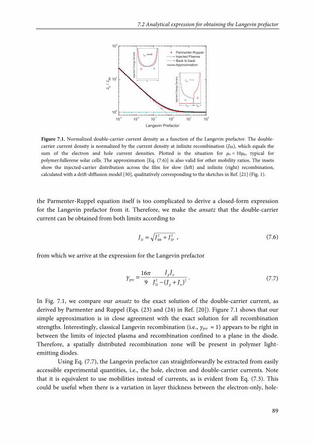
7.2 Analytical expression for obtaining the Langevin prefactor
89
the Parmenter-Ruppel equation itself is too complicated to derive a closed-form expression for the Langevin prefactor from it. Therefore, we make the ansatz that the double-carrier current can be obtained from both limits according to 2
IP2BBD JJJ += , (7.6)
from which we arrive at the expression for the Langevin prefactor
22D
pre )(916
np
np
JJJJJπγ+−
= . (7.7)
In Fig. 7.1, we compare our ansatz to the exact solution of the double-carrier current, as derived by Parmenter and Ruppel (Eqs. (23) and (24) in Ref. [20]). Figure 7.1 shows that our simple approximation is in close agreement with the exact solution for all recombination strengths. Interestingly, classical Langevin recombination (i.e., γpre = 1) appears to be right in between the limits of injected plasma and recombination confined to a plane in the diode. Therefore, a spatially distributed recombination zone will be present in polymer light-emitting diodes.
Using Eq. (7.7), the Langevin prefactor can straightforwardly be extracted from easily accessible experimental quantities, i.e., the hole, electron and double-carrier currents. Note that it is equivalent to use mobilities instead of currents, as is evident from Eq. (7.3). This could be useful when there is a variation in layer thickness between the electron-only, hole-
Figure 7.1. Normalized double-carrier current density as a function of the Langevin prefactor. The double-carrier current density is normalized by the current density at infinite recombination (JBB), which equals the sum of the electron and hole current densities. Plotted is the situation for μn = 10μp, typical for polymer:fullerene solar cells. The approximation [Eq. (7.6)] is also valid for other mobility ratios. The insets show the injected-carrier distribution across the film for slow (left) and infinite (right) recombination, calculated with a drift-diffusion model [30], qualitatively corresponding to the sketches in Ref. [21] (Fig. 1).
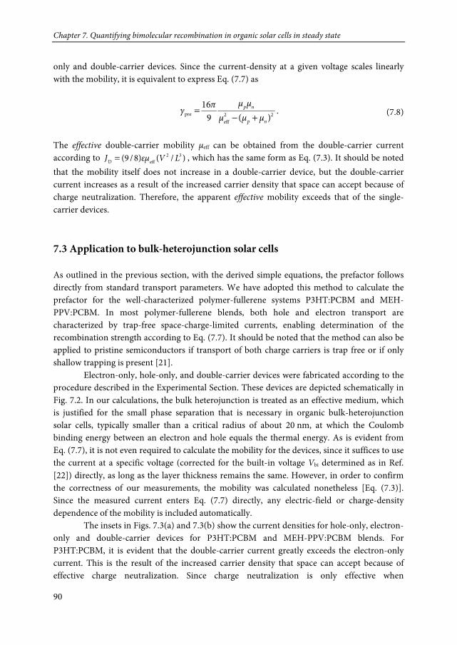
Chapter 7. Quantifying bimolecular recombination in organic solar cells in steady state
90
only and double-carrier devices. Since the current-density at a given voltage scales linearly with the mobility, it is equivalent to express Eq. (7.7) as
22eff
pre )(916
np
np
μμμμμπγ
+−= . (7.8)
The effective double-carrier mobility μeff can be obtained from the double-carrier current according to )/()8/9( 32
effD LVεμJ = , which has the same form as Eq. (7.3). It should be noted that the mobility itself does not increase in a double-carrier device, but the double-carrier current increases as a result of the increased carrier density that space can accept because of charge neutralization. Therefore, the apparent effective mobility exceeds that of the single-carrier devices. 7.3 Application to bulk-heterojunction solar cells
As outlined in the previous section, with the derived simple equations, the prefactor follows directly from standard transport parameters. We have adopted this method to calculate the prefactor for the well-characterized polymer-fullerene systems P3HT:PCBM and MEH-PPV:PCBM. In most polymer-fullerene blends, both hole and electron transport are characterized by trap-free space-charge-limited currents, enabling determination of the recombination strength according to Eq. (7.7). It should be noted that the method can also be applied to pristine semiconductors if transport of both charge carriers is trap free or if only shallow trapping is present [21].
Electron-only, hole-only, and double-carrier devices were fabricated according to the procedure described in the Experimental Section. These devices are depicted schematically in Fig. 7.2. In our calculations, the bulk heterojunction is treated as an effective medium, which is justified for the small phase separation that is necessary in organic bulk-heterojunction solar cells, typically smaller than a critical radius of about 20 nm, at which the Coulomb binding energy between an electron and hole equals the thermal energy. As is evident from Eq. (7.7), it is not even required to calculate the mobility for the devices, since it suffices to use the current at a specific voltage (corrected for the built-in voltage Vbi determined as in Ref. [22]) directly, as long as the layer thickness remains the same. However, in order to confirm the correctness of our measurements, the mobility was calculated nonetheless [Eq. (7.3)]. Since the measured current enters Eq. (7.7) directly, any electric-field or charge-density dependence of the mobility is included automatically. The insets in Figs. 7.3(a) and 7.3(b) show the current densities for hole-only, electron-only and double-carrier devices for P3HT:PCBM and MEH-PPV:PCBM blends. For P3HT:PCBM, it is evident that the double-carrier current greatly exceeds the electron-only current. This is the result of the increased carrier density that space can accept because of effective charge neutralization. Since charge neutralization is only effective when

7.3 Application to bulk-heterojunction solar cells
91
recombination is slow, it is already clear that greatly reduced bimolecular recombination must be present in this device. In the case of MEH-PPV:PCBM, there is less difference between the double-carrier current and the electron-only current, implying that charge neutralization is also less effective. Therefore, recombination should be stronger in this system. By combining the hole, electron and double-carrier currents in Eq. (7.7), the Langevin prefactor can be calculated for every voltage and temperature. In Fig. 7.3(a), the recombination prefactor is plotted against the effective applied voltage for the P3HT:PCBM system. The acquired prefactor has a value of ~3 × 10⁻³ at room temperature, consistent with previously obtained values, typically between 10-4
and 10-2 for several techniques [9,12,13,23-
25]. In comparison, the prefactor obtained for MEH-PPV:PCBM [Fig. 7.3(b)] shows that recombination is much closer to the Langevin equation, with a reduction factor of 0.1-0.3 at room temperature, as can be expected for this system [11,26]. Interestingly, a decreasing Langevin prefactor with decreasing temperatures is observed for both systems, with a slightly more pronounced temperature dependence for MEH-PPV:PCBM. This is in contrast with reported results from photo-CELIV measurements [9,23], although it has been noted that photo-CELIV measurements suffer from a low signal-to-noise ratio and a strong influence of charge injection at higher temperatures, thereby increasing the error margin [14,27]. It has been reported that therefore no temperature dependence of the prefactor could be observed within the error margin for the P3HT:PCBM system [27]. A reduction of the prefactor with decreasing temperature, as we observe here, could correspond to the presence of a potential barrier for recombination [28] that can be
Figure 7.2. Schematic representation of the three types of devices: (a) electron-only device, (b) hole-only device, (c) double-carrier device. The bottom electrodes are biased positively, while the top electrodes are biased negatively (forward bias). The depicted morphology schematically represents the percolative pathways through which the currents flow and should not be confused with a columnar phase separation.
Electron-injecting LiF/Al
- - - -
Hole-blocking Al
Electron-blocking Pd/Au
Hole-injecting Au/PEDOT:PSS
+ + + +
Electron-injecting LiF/Al
- - - -
Hole-injecting Au/PEDOT:PSS
+ + + +
(a)
(b)
(c)
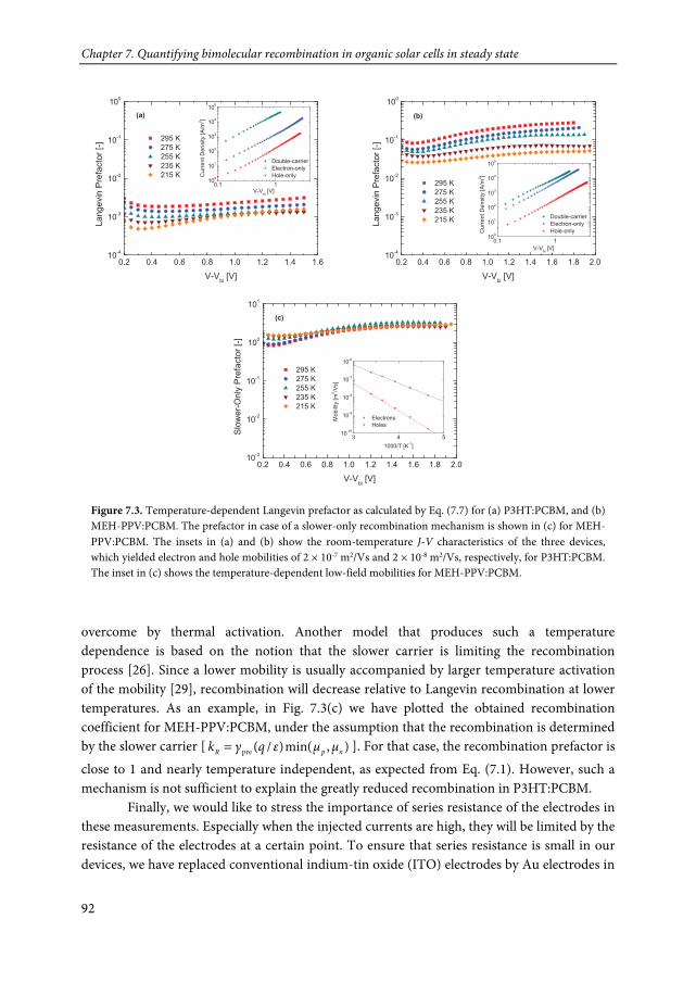
Chapter 7. Quantifying bimolecular recombination in organic solar cells in steady state
92
overcome by thermal activation. Another model that produces such a temperature dependence is based on the notion that the slower carrier is limiting the recombination process [26]. Since a lower mobility is usually accompanied by larger temperature activation of the mobility [29], recombination will decrease relative to Langevin recombination at lower temperatures. As an example, in Fig. 7.3(c) we have plotted the obtained recombination coefficient for MEH-PPV:PCBM, under the assumption that the recombination is determined by the slower carrier [ ),min()/(pre npR μμεqγk = ]. For that case, the recombination prefactor is close to 1 and nearly temperature independent, as expected from Eq. (7.1). However, such a mechanism is not sufficient to explain the greatly reduced recombination in P3HT:PCBM. Finally, we would like to stress the importance of series resistance of the electrodes in these measurements. Especially when the injected currents are high, they will be limited by the resistance of the electrodes at a certain point. To ensure that series resistance is small in our devices, we have replaced conventional indium-tin oxide (ITO) electrodes by Au electrodes in
Figure 7.3. Temperature-dependent Langevin prefactor as calculated by Eq. (7.7) for (a) P3HT:PCBM, and (b) MEH-PPV:PCBM. The prefactor in case of a slower-only recombination mechanism is shown in (c) for MEH-PPV:PCBM. The insets in (a) and (b) show the room-temperature J-V characteristics of the three devices, which yielded electron and hole mobilities of 2 × 10⁻⁷ m2/Vs and 2 × 10⁻⁸ m2/Vs, respectively, for P3HT:PCBM. The inset in (c) shows the temperature-dependent low-field mobilities for MEH-PPV:PCBM.
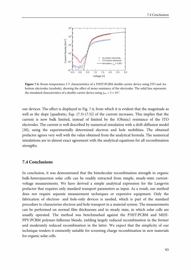
7.4 Conclusions
93
our devices. The effect is displayed in Fig. 7.4, from which it is evident that the magnitude as well as the slope [quadratic; Eqs. (7.3)-(7.5)] of the current increases. This implies that the current is now bulk limited, instead of limited by the (Ohmic) resistance of the ITO electrodes. The current is well described by numerical simulation with a drift-diffusion model [30], using the experimentally determined electron and hole mobilities. The obtained prefactor agrees very well with the value obtained from the analytical formula. The numerical simulations are in almost exact agreement with the analytical equations for all recombination strengths. 7.4 Conclusions In conclusion, it was demonstrated that the bimolecular recombination strength in organic bulk-heterojunction solar cells can be readily extracted from simple, steady-state current-voltage measurements. We have derived a simple analytical expression for the Langevin prefactor that requires only standard transport parameters as input. As a result, our method does not require separate measurement techniques or expensive equipment. Only the fabrication of electron- and hole-only devices is needed, which is part of the standard procedure to characterize electron and hole transport in a material system. The measurements can be performed on normal film thicknesses and in steady state, in which solar cells are usually operated. The method was benchmarked against the P3HT:PCBM and MEH-PPV:PCBM polymer-fullerene blends, yielding largely reduced recombination in the former and moderately reduced recombination in the latter. We expect that the simplicity of our technique renders it eminently suitable for screening charge recombination in new materials for organic solar cells.
Figure 7.4. Room-temperature J-V characteristics of a P3HT:PCBM double-carrier device using ITO and Au bottom electrodes (symbols), showing the effect of series resistance of the electrodes. The solid line represents the simulated characteristics of a double-carrier device using γpre = 3 × 10⁻³.
Chapter 7. Quantifying bimolecular recombination in organic solar cells in steady state
94
Experimental section Device Fabrication: Devices were fabricated on glass substrates that were thoroughly cleaned by washing with detergent solution and ultrasonication in acetone and isopropyl alcohol, followed by UV-ozone treatment. For hole-only and double-carrier devices, a Cr(1 nm)/Au(30 nm) anode was thermally evaporated, followed by spin coating of a hole-injection layer of poly(3,4-ethylenedioxythiophene):poly(styrenesulfonic acid) (PEDOT:PSS; VP AI4083, H.C. Starck). For electron-only devices, Al (30 nm) bottom electrodes were evaporated on the glass substrates. Subsequently, polymer:fullerene blends were spun under N2 atmosphere, using the same solution and spin-coating program for every device type. This process yielded layers of 165 nm for P3HT:PCBM (1:1 by wt. in chloroform) and 120 nm for MEH-PPV:PCBM (1:4 by wt. in chlorobenzene). The P3HT:PCBM layers were annealed in N2 atmosphere for 10 minutes at 140 °C, immediately after deposition. The electron-only and double-carrier devices were finished simultaneously by evaporation of a LiF(1 nm)/Al(100 nm) cathode, while for hole-only devices a Pd(20 nm)/Au(80 nm) top electrode was deposited. Device Characterization: Electrical measurements were conducted under controlled N2 atmosphere, using a computer-controlled Keithley 2400 source meter.
References
95
References
[1] P. W. M. Blom, V. D. Mihailetchi, L. J. A. Koster, and D. E. Markov, Adv. Mater. 19, 1551(2007).
[2] U. Albrecht and H. Bässler, Phys. Status Solidi B 191, 455 (1995).
[3] P. Langevin, Ann. Chim. Phys. 28, 433 (1903).
[4] P. W. M. Blom, M. J. M. de Jong, and S. Breedijk, Appl. Phys. Lett. 71, 930 (1997).
[5] M. Kuik, H. T. Nicolai, M. Lenes, G. A. H. Wetzelaer, M. Lu, and P. W. M. Blom, Appl. Phys. Lett. 98, 093301 (2011).
[6] V. D. Mihailetchi, J. K. J. van Duren, P. W. M. Blom, J. C. Hummelen, R. A. J. Janssen, J. M. Kroon, M. T. Rispens, W. J. H. Verhees, and M. M. Wienk, Adv. Funct. Mater. 13, 43 (2003).
[7] G. A. H. Wetzelaer, M. Kuik, M. Lenes, and P. W. M. Blom, Appl. Phys. Lett. 99, 153506 (2011).
[8] G. A. H. Wetzelaer, M. Kuik, and P. W. M. Blom, Adv. Energy Mater. 2, 1232 (2012).
[9] G. Juška, K. Arlauskas, J. Stuchlik, and R. Österbacka, J. Non-Cryst. Solids 352, 1167 (2006).
[10] G. Juška, K. Genevičius, N. Nekrašas, G. Sliaužys1, and R. Österbacka, Appl. Phys. Lett. 95, 013303 (2009).
[11] A. J. Mozer, N. S. Sariciftci, L. Lutsen, D. Vanderzande, R. Österbacka, M. Westerling, and G. Juška, Appl. Phys. Lett. 86, 112104 (2005).
[12] A. Pivrikas, G. Juška, A. J. Mozer, M. Scharber, K. Arlauskas, N. S. Sariciftci, H. Stubb, and R. Österbacka, Phys. Rev. Lett. 94, 176806 (2005).
[13] G. Juška, K. Arlauskas, G. Sliaužys, A. Pivrikas, A. J. Mozer, N. S. Sariciftci, M. Scharber, and R. Österbacka, Appl. Phys. Lett. 87, 222110 (2005).
[14] A. Baumann, J. Lorrmann, D. Rauh, C. Deibel, and V. Dyakonov, Adv. Mater. 24, 4381 (2012).
[15] M. T. Neukom, N. A. Reinke, and B. Ruhstaller, Solar Energy 85, 1250 (2011).
[16] P. W. M. Blom and M. C. J. M. Vissenberg, Mater. Sci. Eng. R Rep. 27, 53 (2000).

Chapter 7. Quantifying bimolecular recombination in organic solar cells in steady state
96
[17] P. W. M. Blom, M. J. M. de Jong, and J. J. M. Vleggaar, Appl. Phys. Lett. 68, 3308 (1996).
[18] K. C. Kao and W. Hwang, Electrical Transport in Solids (Pergamon Press, Oxford 1981).
[19] N. F. Mott and R. W. Gurney, Electronic Processes in Ionic Crystals (Oxford University Press, London 1940).
[20] R. H. Parmenter and W. Ruppel, J. Appl. Phys. 30, 1548 (1959).
[21] L. M. Rosenberg and M. A. Lampert, J. Appl. Phys. 41, 508 (1970).
[22] G. A. H. Wetzelaer, L. J. A. Koster, and P. W. M. Blom, Phys. Rev. Lett. 107, 066605 (2011).
[23] C. Deibel, A. Baumann, and V. Dyakonov, Appl. Phys. Lett. 93, 163303 (2008).
[24] C. G. Shuttle, B. O’Regan, A. M. Ballantyne, J. Nelson, D. D. C. Bradley, and J. R. Durrant, Phys. Rev. B 78, 113201 (2008).
[25] G. Garcia-Belmonte, P. P. Boix, J. Bisquert, M. Sessolo, and H. J. Bolink, Sol. Energ. Mat. Sol. Cells 94, 366 (2010).
[26] L. J. A. Koster, V. D. Mihailetchi, and P. W. M. Blom, Appl. Phys. Lett. 88, 052104 (2006).
[27] C. Deibel, A. Wagenpfahl, A. Baumann, and V. Dyakonov. Proc. of SPIE 7052, 70520N-1, (2008).
[28] A. J. Ferguson, N. Kopidakis, S. E. Shaheen, and G. Rumbles, J. Phys. Chem. C 115, 23134 (2011).
[29] N. I. Craciun, J. Wildeman, and P.W. M. Blom, Phys. Rev. Lett. 100, 056601 (2008).
[30] L. J. A. Koster, E. C. P. Smits, V. D. Mihailetchi, and P. W. M. Blom, Phys. Rev. B 72, 085205 (2005).
97
Identifying the nature of charge recombination in organic solar cells from charge-transfer state electroluminescence
In this chapter, charge-transfer (CT) state electroluminescence is investigated in several polymer:fullerene bulk-heterojunction solar cells. The ideality factor of the electroluminescence reveals that the CT emission in polymer:fullerene solar cells originates from free-carrier bimolecular recombination at the donor-acceptor interface, rather than a charge-trap-mediated process. The fingerprint of the presence of nonradiative trap-assisted recombination, a voltage-dependent CT electroluminescence quantum efficiency, is only observed for the P3HT:PCBM system, which we explain by a reduction of the competing bimolecular recombination rate. These results are in agreement with measurements of the illumination-intensity dependence of the open-circuit voltage.
8. Nature of recombination in organic solar cells from charge-transfer state electroluminescence
8
Chapter 8. Nature of recombination in organic solar cells from charge-transfer state electroluminescence
98
8.1 Introduction Recombination in low-mobility materials, such as organic semiconductors, is usually described by bimolecular recombination of the Langevin type [1-3], determined by diffusion of free carriers towards each other in their mutual Coulomb field. However, as discussed in the previous chapter, bimolecular recombination in bulk-heterojunction solar cells can be considerably slower than in pristine organic semiconductors. Recently, it has been demonstrated that trapped charges may also take part in the recombination process [4-9]. In that case, a charge carrier is first trapped on an isolated site within the energy band gap, followed by recombination with a mobile carrier of opposite sign, as implied by Shockley-Read-Hall (SRH) statistics [10,11]. The presence of SRH recombination has been identified in all-polymer solar cells [5], organic light-emitting diodes (OLEDs) [6-8] and polymer:fullerene solar cells with intentionally added impurities [4,9].
In addition to inducing a second recombination channel, the presence of traps also limits charge transport in organic semiconductors. As discussed in the introduction of this thesis, it has been observed that the electron transport in organic materials is frequently hindered by electron traps, while hole transport generally shows trap-free behavior [12,13]. As a result, SRH-type recombination via electron traps is naturally present in organic light-emitting diodes made from a single conjugated material [6], as was shown in chapter 3. In an organic solar cell, however, a donor material is used in combination with an acceptor material, so that charge recombination takes place at the donor-acceptor interface. A frequently used acceptor material is the fullerene derivative [6,6]-phenyl-C61-butyric acid methyl ester (PCBM), which shows trap-free electron transport [14]. Consequently, since both hole (donor) and electron (acceptor) traps are absent in polymer:fullerene systems, the electron-hole recombination between the donor and acceptor is expected to be bimolecular. However, recent studies reported on the observation of trap-assisted recombination in polymer:fullerene bulk-heterojunction solar cells [15,16], despite the virtually trap-free electron and hole transport.
To address this issue, we have studied electroluminescence (EL) from the charge-transfer state in polymer:fullerene solar cells. The charge-transfer state emission directly originates from electron-hole recombination at the donor-acceptor interface [17]. In this chapter, we demonstrate that the nature of charge recombination in organic solar cells can be determined by carefully analyzing the bias-dependence of the electroluminescence and its quantum efficiency. 8.2 Ideality factor of the charge-transfer state electroluminescence In the present study, bulk-heterojunction solar cells were fabricated based on a variety of donor polymers blended with a PCBM acceptor. Among the investigated polymers are poly(3-hexylthiophene) (P3HT) and poly[2-methoxy-5-(2’-ethylhexyloxy)-p-phenylenevinylene]

8.2 Ideality factor of the charge-transfer state electroluminescence
99
(MEH-PPV), which have served as workhorses in organic photovoltaic research [18,19]. The other two polymers used in this study are poly[9,9-didecanefluorene-alt-(bis-thienylene) benzothiadiazole] (PF10TBT) and poly[2,6-(4,4-bis-(2-ethylhexyl)-4H-cyclopenta[2,1-b;3,4-b’]-dithiophene)-alt-4,7-(2,1,3-benzothiadiazole)] (PCPDTBT). These are more recent wide- and narrow-bandgap polymers, respectively, capable of giving power-conversion efficiencies between 4 and 6% [20,21]. Hence, homopolymers as well as copolymers with distinct chemical and physical properties are used, to demonstrate the generality of our approach. In chapter 3, we demonstrated for OLEDs that the recombination mechanism, either bimolecular or trap-assisted recombination, is directly reflected in the ideality factor of the current and light output [6]. This ideality factor appears in the general Shockley diode equation, given by [22]
−
= 1exp0 kTη
qVJJ , (8.1)
where J is the current density, J0 the (reverse bias) saturation current density, V the applied voltage, q the elementary charge, k Boltzmann’s constant, T temperature, and η the ideality factor. The ideality factor equals unity in an ideal classical p-n junction diode with only direct recombination taking place. However, as shown in 1957 by a theoretical analysis of Sah, Noyce and Shockley, the presence of SRH recombination results in an enhancement of the ideality factor, reaching a value of 2 for dominant trap-assisted recombination [23]. In chapter 3, the difference in ideality factor for bimolecular (η = 1) and trap-assisted recombination (η = 2) has been visualized in the different voltage dependence of the red and blue emission of white-emitting OLEDs, where both bimolecular (blue) and trap-assisted recombination (red) are emissive [6]. As a result, the ideality factor can be used as a fingerprint for the presence or absence of SRH recombination.
Ideality factors larger than unity have also been found in the dark current of polymer:fullerene solar cells, which is frequently put forward as evidence for the presence of a dominant trap-assisted recombination process [15,16]. However, in chapter 6 it was demonstrated that in this case the greater-than-unity ideality factor is caused by enhanced diffusion due to violation of the classical Einstein relation [24]. As a result, an ideality factor above unity can be measured even when trap-assisted recombination is completely absent [25]. The dark-current ideality factor of a polymer:fullerene bulk-heterojunction solar cell therefore cannot give conclusive information about the presence or absence of trap-assisted recombination.
As described in a recent study by Tvingstedt et al. [17], recombination at the polymer-fullerene interface is directly observable from the electroluminescence of the charge-transfer state. Charge-transfer state electroluminescence can be detected by applying a forward voltage across the solar cell and measuring the resulting emission with a silicon photodiode. Thus, the solar cell is simply operated as a light-emitting diode. As stated above, the different recombination mechanisms can directly be identified by measuring the luminance (L) ideality
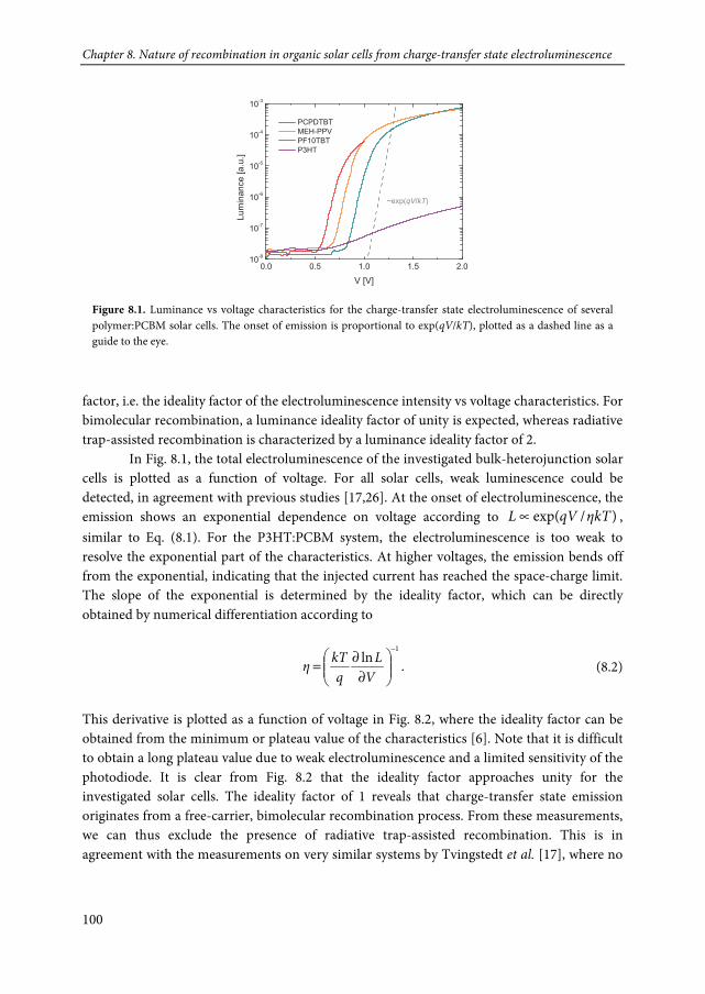
Chapter 8. Nature of recombination in organic solar cells from charge-transfer state electroluminescence
100
factor, i.e. the ideality factor of the electroluminescence intensity vs voltage characteristics. For bimolecular recombination, a luminance ideality factor of unity is expected, whereas radiative trap-assisted recombination is characterized by a luminance ideality factor of 2.
In Fig. 8.1, the total electroluminescence of the investigated bulk-heterojunction solar cells is plotted as a function of voltage. For all solar cells, weak luminescence could be detected, in agreement with previous studies [17,26]. At the onset of electroluminescence, the emission shows an exponential dependence on voltage according to )/exp( kTηqVL ∝ , similar to Eq. (8.1). For the P3HT:PCBM system, the electroluminescence is too weak to resolve the exponential part of the characteristics. At higher voltages, the emission bends off from the exponential, indicating that the injected current has reached the space-charge limit. The slope of the exponential is determined by the ideality factor, which can be directly obtained by numerical differentiation according to
1
ln−
∂
∂=V
Lq
kTη . (8.2)
This derivative is plotted as a function of voltage in Fig. 8.2, where the ideality factor can be obtained from the minimum or plateau value of the characteristics [6]. Note that it is difficult to obtain a long plateau value due to weak electroluminescence and a limited sensitivity of the photodiode. It is clear from Fig. 8.2 that the ideality factor approaches unity for the investigated solar cells. The ideality factor of 1 reveals that charge-transfer state emission originates from a free-carrier, bimolecular recombination process. From these measurements, we can thus exclude the presence of radiative trap-assisted recombination. This is in agreement with the measurements on very similar systems by Tvingstedt et al. [17], where no
Figure 8.1. Luminance vs voltage characteristics for the charge-transfer state electroluminescence of several polymer:PCBM solar cells. The onset of emission is proportional to exp(qV/kT), plotted as a dashed line as a guide to the eye.
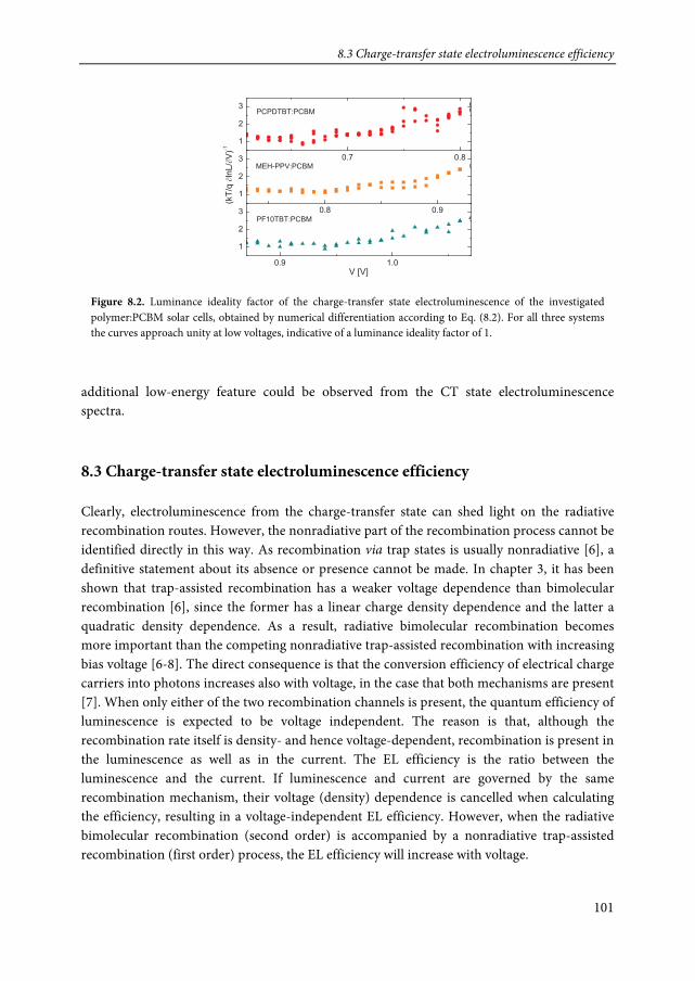
8.3 Charge-transfer state electroluminescence efficiency
101
additional low-energy feature could be observed from the CT state electroluminescence spectra. 8.3 Charge-transfer state electroluminescence efficiency Clearly, electroluminescence from the charge-transfer state can shed light on the radiative recombination routes. However, the nonradiative part of the recombination process cannot be identified directly in this way. As recombination via trap states is usually nonradiative [6], a definitive statement about its absence or presence cannot be made. In chapter 3, it has been shown that trap-assisted recombination has a weaker voltage dependence than bimolecular recombination [6], since the former has a linear charge density dependence and the latter a quadratic density dependence. As a result, radiative bimolecular recombination becomes more important than the competing nonradiative trap-assisted recombination with increasing bias voltage [6-8]. The direct consequence is that the conversion efficiency of electrical charge carriers into photons increases also with voltage, in the case that both mechanisms are present [7]. When only either of the two recombination channels is present, the quantum efficiency of luminescence is expected to be voltage independent. The reason is that, although the recombination rate itself is density- and hence voltage-dependent, recombination is present in the luminescence as well as in the current. The EL efficiency is the ratio between the luminescence and the current. If luminescence and current are governed by the same recombination mechanism, their voltage (density) dependence is cancelled when calculating the efficiency, resulting in a voltage-independent EL efficiency. However, when the radiative bimolecular recombination (second order) is accompanied by a nonradiative trap-assisted recombination (first order) process, the EL efficiency will increase with voltage.
Figure 8.2. Luminance ideality factor of the charge-transfer state electroluminescence of the investigated polymer:PCBM solar cells, obtained by numerical differentiation according to Eq. (8.2). For all three systems the curves approach unity at low voltages, indicative of a luminance ideality factor of 1.
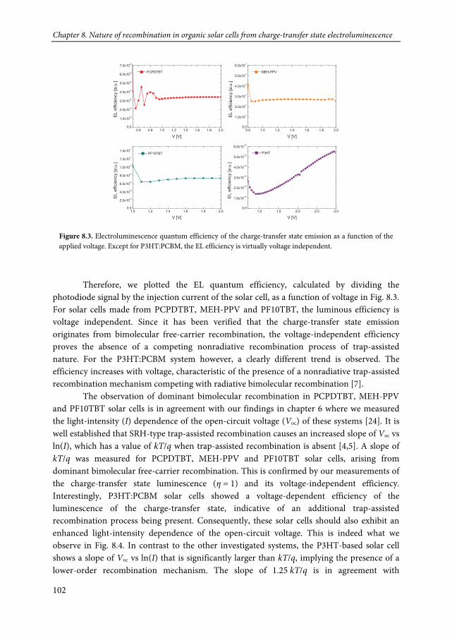
Chapter 8. Nature of recombination in organic solar cells from charge-transfer state electroluminescence
102
Therefore, we plotted the EL quantum efficiency, calculated by dividing the photodiode signal by the injection current of the solar cell, as a function of voltage in Fig. 8.3. For solar cells made from PCPDTBT, MEH-PPV and PF10TBT, the luminous efficiency is voltage independent. Since it has been verified that the charge-transfer state emission originates from bimolecular free-carrier recombination, the voltage-independent efficiency proves the absence of a competing nonradiative recombination process of trap-assisted nature. For the P3HT:PCBM system however, a clearly different trend is observed. The efficiency increases with voltage, characteristic of the presence of a nonradiative trap-assisted recombination mechanism competing with radiative bimolecular recombination [7]. The observation of dominant bimolecular recombination in PCPDTBT, MEH-PPV and PF10TBT solar cells is in agreement with our findings in chapter 6 where we measured the light-intensity (I) dependence of the open-circuit voltage (Voc) of these systems [24]. It is well established that SRH-type trap-assisted recombination causes an increased slope of Voc vs ln(I), which has a value of kT/q when trap-assisted recombination is absent [4,5]. A slope of kT/q was measured for PCPDTBT, MEH-PPV and PF10TBT solar cells, arising from dominant bimolecular free-carrier recombination. This is confirmed by our measurements of the charge-transfer state luminescence (η = 1) and its voltage-independent efficiency. Interestingly, P3HT:PCBM solar cells showed a voltage-dependent efficiency of the luminescence of the charge-transfer state, indicative of an additional trap-assisted recombination process being present. Consequently, these solar cells should also exhibit an enhanced light-intensity dependence of the open-circuit voltage. This is indeed what we observe in Fig. 8.4. In contrast to the other investigated systems, the P3HT-based solar cell shows a slope of Voc vs ln(I) that is significantly larger than kT/q, implying the presence of a lower-order recombination mechanism. The slope of 1.25 kT/q is in agreement with
Figure 8.3. Electroluminescence quantum efficiency of the charge-transfer state emission as a function of the applied voltage. Except for P3HT:PCBM, the EL efficiency is virtually voltage independent.

8.3 Charge-transfer state electroluminescence efficiency
103
previously obtained values [27] and once more confirms the interpretation of the voltage-dependent EL efficiency. It should be noted that similar slopes were obtained using P3HT obtained from different sources (see Experimental Section) and processing the films from different solvents. The qualitative agreement of the EL ideality factor and efficiency measurements with the intensity dependence of Voc shows that our electroluminescence measurements are a relevant representation of recombination mechanisms in organic solar cells under operating conditions. Important in the comparison between recombination of photogenerated and voltage-generated charges is the electric-field and charge-density regime in which the measurements are performed. The ideality factor of the CT-state electroluminescence is obtained in the voltage regime just below the open-circuit voltage, which is actually close to the voltage of the maximum-power point. As the measurements are performed near flat-band condictions and in dark, the charge density in the EL ideality factor experiment is lower than under illumination. Since trap-assisted recombination (if present) is more dominant at lower densities [6,7], the amount of trap-assisted recombination is expected to be even lower under illumination.
The EL efficiency measurements are performed in a regime where the effective applied electric field is similar to the fields in solar cells under operating conditions (although in opposite direction). As charge density is increased with applied voltage, a crossover from trap-assisted (if present) to bimolecular recombination is expected to occur in a certain voltage range, which is observed only for P3HT. As a result, it can be concluded that trap-assisted recombination plays a role in a P3HT:PCBM solar cell both in dark and under illumination.
Figure 8.4. Normalized Voc vs incident light intensity for the investigated polymer:fullerene solar cells. For P3HT:PCBM, the best fit to the data (solid line) has a slope (S) of 1.25 kT/q. The other investigated cells are well described by a line with a slope of kT/q. The Voc was normalized by addition of a constant so that the best fits of the separate datasets coincide at an intensity of 1400 W/m2.

Chapter 8. Nature of recombination in organic solar cells from charge-transfer state electroluminescence
104
8.4 Trap-assisted recombination in P3HT:PCBM Although both independent EL and Voc measurements indicate a substantial influence of an SRH-type recombination channel in P3HT:PCBM, the occurrence of this mechanism is not straightforward. The appearance of trap-assisted recombination requires the presence of a density of trap states, which should give rise to the observation trap-limited charge transport. However, the transport characteristics as measured in single-carrier diodes of P3HT and PCBM show trap-free behavior, which contradicts the presence of a large trap density.
This apparent discrepancy can be resolved by considering the fact that recombination of free and trapped carriers are competing processes. As a consequence, the observation of a SRH mechanism can also be due to a reduced bimolecular recombination rate. Bimolecular recombination in organic semiconductors is usually of the Langevin type. As discussed in the previous chapter, greatly reduced bimolecular recombination rates have been measured for the P3HT:PCBM system [28-30]. The experimentally obtained value for the bimolecular recombination coefficient in those cells is approximately a factor of 1000 lower than for conventional Langevin recombination.
Since the bimolecular Langevin recombination rate is greatly reduced in the P3HT:PCBM system, it is expected that SRH recombination can become apparent even when the trap density is small. To investigate at which trap density the transport is affected such that it can be observed experimentally, numerical drift-diffusion simulations[31] were carried out. Figure 8.5 shows simulations of the J-V characteristics of a P3HT hole-only diode for increasing hole-trap densities. It is clear that the effect of charge trapping on the hole current becomes negligible at trap densities below 2 × 10²¹ m-3, and hence impossible to observe from experimental J-V characteristics.
The next step is to investigate whether such low trap densities are sufficient to explain the light-intensity dependence of Voc when a reduced bimolecular recombination rate is taken into account. Therefore, current-voltage characteristics of a P3HT:PCBM solar cell were
Figure 8.5. Experimental (symbols) and simulated (lines) J-V characteristics of a P3HT hole-only device. The simulations are performed for increasing hole-trap densities [m-3] of a single-level trap with a depth of 0.5 eV.
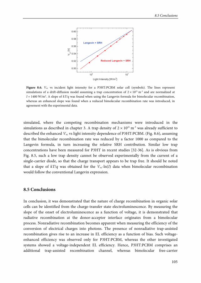
8.5 Conclusions
105
simulated, where the competing recombination mechanisms were introduced in the simulations as described in chapter 3. A trap density of 2 × 10²¹ m-3 was already sufficient to described the enhanced Voc vs light intensity dependence of P3HT:PCBM. (Fig. 8.6), assuming that the bimolecular recombination rate was reduced by a factor 1000 as compared to the Langevin formula, in turn increasing the relative SRH contribution. Similar low trap concentrations have been measured for P3HT in recent studies [32-36]. As is obvious from Fig. 8.5, such a low trap density cannot be observed experimentally from the current of a single-carrier diode, so that the charge transport appears to be trap free. It should be noted that a slope of kT/q was obtained for the Voc-ln(I) data when bimolecular recombination would follow the conventional Langevin expression. 8.5 Conclusions In conclusion, it was demonstrated that the nature of charge recombination in organic solar cells can be identified from the charge-transfer state electroluminescence. By measuring the slope of the onset of electroluminescence as a function of voltage, it is demonstrated that radiative recombination at the donor-acceptor interface originates from a bimolecular process. Nonradiative recombination becomes apparent when measuring the efficiency of the conversion of electrical charges into photons. The presence of nonradiative trap-assisted recombination gives rise to an increase in EL efficiency as a function of bias. Such voltage-enhanced efficiency was observed only for P3HT:PCBM, whereas the other investigated systems showed a voltage-independent EL efficiency. Hence, P3HT:PCBM comprises an additional trap-assisted recombination channel, whereas bimolecular free-carrier
Figure 8.6. Voc vs incident light intensity for a P3HT:PCBM solar cell (symbols). The lines represent simulations of a drift-diffusion model assuming a trap concentration of 2 × 10²¹ m-3 and are normalized at I = 1400 W/m2. A slope of kT/q was found when using the Langevin formula for bimolecular recombination, whereas an enhanced slope was found when a reduced bimolecular recombination rate was introduced, in agreement with the experimental data.
Chapter 8. Nature of recombination in organic solar cells from charge-transfer state electroluminescence
106
recombination is dominant in the other solar cells. Ultimately, this was confirmed by measurements on the light intensity-dependence of the open-circuit voltage. The manifestation of SRH-type trap-assisted recombination in P3HT:PCBM bulk-heterojunction solar cells is attributed to a reduced competing bimolecular recombination rate. In that case, a small number of trapping sites is sufficient to cause an enhanced light-intensity dependence of Voc, while having only a minor effect on charge transport. Experimental section Device Fabrication: For the fabrication of the polymer:fullerene solar cells, glass substrates, prepatterned with indium tin oxide, were thoroughly cleaned by washing with detergent solution and ultrasonication in acetone and isopropyl alcohol, followed by UV-ozone treatment. The cleaned substrates were coated in ambient air with a 60 nm film of poly(3,4-ethylenedioxythiophene):poly(styrenesulfonic acid) (VP AI4083, H.C. Starck). Subsequently, photoactive layers with a thickness of 80-100 nm of PCPDTBT:PCBM (1:2), MEH-PPV:PCBM (1:4), PF10TBT:PCBM (1:4) and P3HT:PCBM (1:1) were deposited by spin coating from chlorobenzene solution under N2 atmosphere. The P3HT:PCBM layers were annealed in N2 atmosphere for 10 minutes at 140 °C, immediately after deposition. The devices were finished by thermal evaporation of a LiF(1 nm)/Al(100 nm) cathode at a base pressure of 1 × 10⁻⁶ mbar. Hole-only devices were fabricated similarly in a glass/ITO/PEDOT:PSS/P3HT/Au structure. P3HT was obtained from Rieke Metals, Inc. (4002-EE) and Plextronics, Inc. (Plexcore® OS 2100). Device Characterization: Electrical measurements were conducted under controlled N2 atmosphere, using a computer-controlled Keithley 2400 source meter. Electroluminescence was recorded simultaneously using a Hamamatsu S1336 silicon photodiode. For the measurements under illumination, a Steuernagel SolarConstant 1200 metal halide lamp was used, which was set to 1 sun intensity using a silicon reference cell and correcting for spectral mismatch. Intensity-dependent measurements were performed by using a set of neutral-density filters to decrease the illumination level.
References
107
References
[1] P. Langevin, Ann. Chim. Phys. 28, 433 (1903).
[2] P. W. M. Blom, M. J. M. de Jong, and S. Breedijk, Appl. Phys. Lett. 71, 930 (1997).
[3] A. Pivrikas, G. Juška, R. Österbacka, M. Westerling, M. Viliūnas, K. Arlauska, and H. Stubb, Phys. Rev. B 71, 125205 (2005).
[4] M. M. Mandoc, F. B. Kooistra, J. C. Hummelen, B. de Boer, and P. W. M. Blom, Appl. Phys. Lett. 91, 263505 (2007).
[5] M. M. Mandoc, W. Veurman, L. J. A. Koster, B. de Boer, and P. W. M. Blom, Adv. Funct. Mater. 17, 2167 (2007).
[6] G. A. H. Wetzelaer, M. Kuik, H. T. Nicolai, and P. W. M. Blom, Phys. Rev. B 83, 165204 (2011).
[7] M. Kuik, H. T. Nicolai, M. Lenes, G. A. H. Wetzelaer, M. Lu, and P. W. M. Blom, Appl. Phys. Lett. 98, 093301 (2011).
[8] M. Kuik, L. J. A. Koster, G. A. H. Wetzelaer, and P. W. M. Blom, Phys. Rev. Lett. 107, 256805 (2011).
[9] S. R. Cowan, W. L. Leong, N. Banerji, G. Dennler, and A. J. Heeger, Adv. Funct. Mater. 21, 3083 (2011).
[10] W. Shockley and W. T. Read, Phys. Rev. 87, 835(1952).
[11] R. N. Hall, Phys. Rev. 83, 228 (1951); ibid. 87, 387 (1952).
[12] P. W. M. Blom, M. J. M. de Jong, and J. J. M. Vleggaar, Appl. Phys. Lett. 68, 3308 (1996).
[13] M. M. Mandoc, B. de Boer, G. Paasch, and P. W. M. Blom, Phys. Rev. B 75, 193202 (2007).
[14] V. D. Mihailetchi, J. K. J. van Duren, P. W. M. Blom, J. C. Hummelen, R. A. J. Janssen, J. M. Kroon, M. T. Rispens, W. J. H. Verhees, and M. M. Wienk, Adv. Funct. Mater. 13, 43 (2003).
[15] R. A. Street, M. Schoendorf, A. Roy, and J. H. Lee, Phys. Rev. B 81, 205307 (2010).
[16] T. Kirchartz, B. E. Pieters, J. Kirkpatrick, U. Rau, and J. Nelson, Phys. Rev. B 83, 115209 (2011).
Chapter 8. Nature of recombination in organic solar cells from charge-transfer state electroluminescence
108
[17] K. Tvingstedt, K. Vandewal, A. Gadisa, F. Zhang, J. Manca, and O. Inganas, J. Am. Chem. Soc. 131, 11819 (2009).
[18] G. Yu, J. Gao, J. C. Hummelen, F. Wudl, and A. J. Heeger, Science 270, 1789 (1995).
[19] F. Padinger, R. S. Ritterberger, and N. S. Sariciftci, Adv. Funct. Mater. 13, 85 (2003).
[20] L. H. Slooff, S. C. Veenstra, J. M. Kroon, D. J. D. Moet, J. Sweelssen, and M. M. Koetse, Appl. Phys. Lett. 90, 143506 (2007).
[21] J. Peet, J. Y. Kim, N. E. Coates, W. L. Ma, D. Moses, A. J. Heeger, and G. C. Bazan, Nat. Mater. 6, 497 (2007).
[22] W. Shockley, Bell Syst. Tech. J. 28, 435 (1949).
[23] C. T. Sah, R. N. Noyce, and W. Shockley, Proc. IRE 45, 1228 (1957).
[24] G. A. H. Wetzelaer, M. Kuik, M. Lenes, and P. W. M. Blom, Appl. Phys. Lett. 99, 153506 (2011).
[25] G. A. H. Wetzelaer, L. J. A. Koster, and P. W. M. Blom, Phys. Rev. Lett. 107, 066605 (2011).
[26] K. Vandewal, K. Tvingstedt, A. Gadisa, O. Inganäs, and J. V. Manca, Nat. Mater. 8, 904 (2009).
[27] M. Lenes, S. W. Shelton, A. B. Sieval, D. F. Kronholm, J. C. Hummelen, and P. W. M. Blom, Adv. Funct. Mater. 19, 3002 (2009).
[28] A. Pivrikas, G. Juška, A. J. Mozer, M. Scharber, K. Arlauskas, N. S. Sariciftci, H. Stubb, and R. Österbacka, Phys. Rev. Lett. 94, 176806 (2005).
[29] G. Juška, K. Arlauskas, J. Stuchlik, and R. Österbacka, J. Non-Cryst. Solids 352, 1167 (2006).
[30] C. Deibel, A. Baumann, and V. Dyakonov, Appl. Phys. Lett. 93, 163303 (2008).
[31] L. J. A. Koster, E. C. P. Smits, V. D. Mihailetchi, and P. W. M. Blom, Phys. Rev. B 72, 085205 (2005).
[32] J. Schafferhans, A. Baumann, C. Deibel, and V. Dyakonov, Appl. Phys. Lett. 93, 093303 (2008).
[33] G. Garcia-Belmonte, P. P. Boix, J. Bisquert, M. Sessolo, and H. J. Bolink, Sol. Energy Mater. Sol. Cells 94, 366 (2010).
References
109
[34] K. S. Nalwa, R. C. Mahadevapuram, and S. Chaudhary, Appl. Phys. Lett. 98, 093306 (2011).
[35] S. Khelifi, K. Decock, J. Lauwaert, H. Vrielinck, D. Spoltore, F. Piersimoni, J. Manca, A. Belghachi, and M. Burgelman, J. Appl. Phys. 110, 094509 (2011).
[36] P. P. Boix, J. Ajuria, I. Etxebarria, R. Pacios, and G. Garcia-Belmonte, Thin Solid Films 520, 2265 (2012).

111
Summary
| Summary Organic semiconductors are a very attractive class of materials. Like classical inorganic semiconductors, organic semiconductors can serve as the active component in electronic devices, such as solar cells, light-emitting diodes, and field-effect transistors. The attraction towards organic electronics stems from a number of advantages: organic semiconductors are typically lightweight, flexible, (semi)transparent, and easy to process. In addition, there are an almost infinite number of possibilities for tuning the chemical structure of these organic properties, resulting in an equal number of distinct optoelectronic properties. As a result, also in that respect, organic semiconductors comprise a large flexibility. However, despite the abundance in future potential, there are still some issues that have to be solved for organic-semiconductor devices to compete with present-day technology. Most importantly, performance and lifetime have to be increased. In order to improve the performance of organic-semiconductor devices, a fundamental understanding of the device physics is indispensable. This thesis focuses on the properties of charge transport and recombination in organic-semiconductor diodes. The most important organic devices that comprise a diode structure are organic solar cells and organic light-emitting diodes (OLEDs). Organic solar cells convert sunlight into electrical energy, while OLEDs produce light upon the application of electrical energy. Two of the main processes that govern the operation of these diodes are the transport and recombination of charge carriers. Charge transport describes the movement of charges through the semiconductor. In an OLED, injected electrons and holes are transported through the organic semiconductor, after which the recombination process can occur. In an organic solar cell, photogenerated charge carriers are transported toward the electrodes to produce an electrical current. As organic semiconductors typically have a disordered conformation when processed into a thin film, also their energetic properties are subject to disorder. As such, charge transport occurs via a phonon-assisted hopping process through a landscape of energetically-distributed localized states. Therefore, charge transport has vastly distinct properties as compared to band conduction in classical inorganic semiconductors. In addition, charge transport can be hindered by so-called trapping sites, which are energetically-favorable isolated states that can trap mobile charges that move through the organic semiconductor. Next to the charge-transport process, also the recombination of charge carriers plays an important role in organic diodes. When an electron and a hole meet, they may recombine, which can result in the emission of a photon. In an OLED, the recombination process is responsible for the light emission, while in a solar cell, recombination is a loss mechanism. In the latter case, photogenerated charges are annihilated in the recombination process and can

Summary
112
no longer contribute to the generation of an electrical current. It is evident that a fundamental understanding of charge transport and recombination is necessary to improve the performance of organic-semiconductor diodes. In chapter 2 of this thesis, charge transport is investigated in a donor-acceptor copolymer. Remarkably, it is observed that both electron and hole transport are trap free, which is uncommon for an organic semiconductor. In many cases, electron transport shows distinct trapping behavior and is inferior to hole transport. Due to the large electron affinity of the investigated copolymer, the commonly-observed trapping sites are no longer energetically favorable and electron transport shows trap-free behavior. In addition, the electron mobility is observed to be more than two orders of magnitude higher than the hole mobility, which is explained by quantum chemical calculations. These results show that electron trapping can be avoided by using materials with deep energy levels. In chapter 3, it is demonstrated that electron traps do not only hinder charge transport, but also negatively affect the recombination process. By studying the diode ideality factor of single-layer OLEDs, it is observed that trap-assisted recombination occurs in these devices, competing with radiative bimolecular free-carrier recombination. Trap-assisted recombination is identified as a nonradiative process that is dominant at low driving voltages. Because of its nonradiative nature, trap-assisted recombination is a loss mechanism in OLEDs. The two competing recombination mechanisms can be disentangled by studying the luminance ideality factor of a white-emitting polymer, in which both trap-assisted and bimolecular recombination are radiative.
The physical origin of trap-assisted recombination in organic semiconductors is investigated in the following chapter. It is demonstrated that the rate-limiting step for this recombination mechanism is the diffusion of free holes towards trapped electrons in their mutual Coulomb field. As a result, the trap-assisted recombination rate follows directly from the hole mobility, allowing quantification of this loss mechanism.
While the ideality factor can be used as a fingerprint for the present recombination mechanism, the origin of the ideality factor in single-carrier diodes, in which recombination is absent, is unclear. The regime in the current-voltage characteristics from which the ideality factor is determined is dominated by the diffusion of charge carriers. Previous research suggests that diffusion in disordered semiconductors does not obey the classical Einstein relation, which connects the kinetic coefficients of diffusivity and mobility. Studying the diffusion-driven current in single-carrier diodes, however, shows that the Einstein relation is violated only under nonequilibrium conditions, due to the presence of deeply-trapped carriers. Removal of these deeply-trapped carriers by recombination proves the validity of the classical Einstein relation in disordered semiconductors in thermal (quasi)equilibrium.
With the increased knowledge about diffusion currents in OLEDs and single-carrier devices, the dark-current ideality factors of polymer:fullerene bulk-heterojunction solar cells are examined in chapter 6. In a solar cell, both electron and hole transport show trap-free behavior. While also for such solar cells a deviation of the ideality factor from unity is commonly ascribed to the presence of trap-assisted recombination, it is demonstrated that
Summary
113
this does not have to be the case. Like in a single-carrier diode, the ideality factor can deviate from unity, even in the absence of recombination. It is demonstrated that trap-assisted recombination is absent, while the nonideality is caused by the transport properties of the transport-dominating constituent of the donor:acceptor blend.
Since trap-assisted recombination typically plays a minor role in organic solar cells, bimolecular recombination is the most important loss mechanism. However, the bimolecular recombination rate frequently appears to be reduced with respect to the expected Langevin rate. Therefore, a steady-state technique to quantify the bimolecular recombination rate is introduced in chapter 7. It is observed that the recombination rate in the P3HT:PCBM system is reduced by about three orders of magnitude as compared to Langevin recombination. For other systems, the reduction is substantially less pronounced. The absence of trap-assisted recombination in organic solar is further substantiated in chapter 8. Here, it is demonstrated that emission from the charge-transfer state has a bimolecular origin, evidenced by the luminance ideality factor. Studying the voltage dependence of the electroluminescence quantum efficiency reveals that nonradiative trap-assisted recombination is absent in most polymer:fullerene blends. However, it is shown that in the P3HT:PCBM system a significant contribution of trap-assisted recombination is present. Since it has been demonstrated in chapter 7 that bimolecular recombination is very weak in this system, a competing trap-assisted recombination mechanism from a small number of traps can become apparent.

115
Samenvatting
| Samenvatting Organische halfgeleiders vormen een zeer aantrekkelijke klasse van materialen. Net zoals klassieke anorganische halfgeleiders kunnen organische halfgeleiders dienen als de actieve component in elektronische schakelingen, zoals zonnecellen, lichtuitstralende diodes (leds) en veldeffecttransistors. De aantrekkelijkheid van organische elektronica vindt zijn oorsprong in een aantal voordelen: organische halfgeleiders zijn typisch licht in gewicht, flexibel, lichtdoorlatend en eenvoudig te verwerken. Bovendien zijn er ontelbare mogelijkheden voor het aanpassen van de chemische structuur, hetgeen resulteert in een overeenkomstige verscheidenheid aan opto-elektronische eigenschappen. Ook in dat opzicht bezitten organische halfgeleiders dus een grote flexibiliteit.
Ondanks de overvloed aan toekomstperspectief resteren er echter enkele problemen die opgelost dienen te worden alvorens toepassingen op basis van organische halgeleiders kunnen concurreren met de huidige technologie. Voorop staat dat de prestaties en levensduur moeten worden verbeterd. Om de prestaties te verbeteren is een fundamenteel inzicht in de fysica van deze organische elektronische componenten onmisbaar.
Dit proefschrift richt zich op de eigenschappen van ladingstransport en -recombinatie in organische halfgeleiderdiodes. De belangrijkste organische componenten met een diodestructuur zijn organische zonnecellen en organische leds (OLEDs). Organische zonnecellen zetten zonlicht om in elektrische energie, terwijl OLEDs licht produceren uit elektrische energie. Twee van de belangrijkste processen die de werking van deze diodes bepalen zijn het transport en de recombinatie van ladingsdragers.
Ladingstransport is het proces van het bewegen van ladingen door de halfgeleider. In een OLED bewegen geïnjecteerde elektronen en gaten zich door de organische halfgeleider, wat kan leiden tot het recombinatieproces. In een organische zonnecel worden onder belichting vrije ladingsdragers gecreëerd die zich vervolgens naar de elektrodes bewegen, wat resulteert in een elektrische stroom. Omdat organische halfgeleidermoleculen in een dunne laag zich vaak wanordelijk schikken zijn ook hun energetische eigenschappen onderhevig aan wanorde. Dit heeft als gevolg dat ladingstransport plaatsvindt via een fonon-geassisteerd hopping proces door een landschap van energetisch verdeelde gelokaliseerde toestanden. Daarom heeft het ladingstransport duidelijk verschillende eigenschappen in vergelijking met het bandtransport in klassiek halfgeleiders. Verder kan het landingstransport gehinderd worden door zogenaamde ladingsvallen (Engels: traps), wat energetisch gunstige, geïsoleerde toestanden zijn die mobiele ladingen kunnen invangen die zich door de organische halfgeleider bewegen.
Behalve het ladingstransport speelt ook de recombinatie van ladingsdragers een belangrijke rol in organische diodes. Wanneer een elektron en een gat elkaar tegenkomen
Samenvatting
116
kunnen ze recombineren, wat kan resulteren in het uitzenden van een foton. In een OLED is het recombinatieproces verantwoordelijk voor het uitzenden van licht, terwijl recombinatie een verliesmechanisme is in een zonnecel. In het tweede geval worden fotogegeneerde ladingen vernietigd in het recombinatieproces en kunnen derhalve niet meer bijdragen aan de opgewekte elektrische stroom. Het is evident dat een fundamenteel begrip van ladingstransport en -recombinatie noodzakelijk is om de prestaties van organische halfgeleiderdiodes te verbeteren.
In hoofdstuk 2 van dit proefschrift wordt ladingstransport in een donor-acceptor copolymeer onderzocht. Opmerkelijk is dat het transport van zowel elektronen als gaten niet gehinderd wordt door ladingsvallen, wat vrij ongebruikelijk is voor een organische halfgeleider. In veel gevallen wordt het elektronentransport sterkt gehinderd door ladingsvallen en is daardoor minder goed dan het gatentransport. Als gevolg van de grote elektronenaffiniteit van het onderzochte copolymeer zijn de gebruikelijke ladingsvallen niet meer energetisch gunstig gelegen, waardoor ze geen ladingen meer kunnen invangen. Voorts blijkt de elektronenmobiliteit meer dan twee ordes van grootte hoger te zijn dan de gatenmobiliteit, wat verklaard wordt met kwantumchemische berekeningen. Deze resultaten tonen aan dat het invangen van elektronen in ladingsvallen kan worden vermeden door materialen te gebruiken met diepe energieniveaus.
In hoofdstuk 3 wordt aangetoond dat ladingsvallen niet alleen het ladingstransport hinderen, maar ook het recombinatieproces negatief beïnvloeden. Door de idealiteitsfactor van enkellaags OLEDs te bestuderen wordt het duidelijk dat trap-geassisteerde recombinatie plaatsvindt, concurrerend met de bimoleculaire recombinatie van vrije ladingsdragers. Trap-geassisteerde recombinatie wordt geïdentificeerd als een proces dat niet tot het uitzenden van een foton leidt en dominant is bij een lage aangelegde spanning. Omdat deze vorm van recombinatie niet leidt tot het uitzenden van licht is het een verliesmechanisme in OLEDs. De twee concurrerende recombinatieprocessen kunnen worden onderscheiden door de idealiteitsfactor van het licht van een witte OLED te bestuderen, waarin zowel de bimoleculaire als de trap-geassisteerde recombinatie leiden tot het uitzenden van licht.
De fysische oorzaak van trap-geassisteerde recombinatie wordt onderzocht in het daaropvolgende hoofdstuk. Het wordt aangetoond dat de snelheidsbepalende stap in dit proces de diffusie van vrije gaten richting ingevangen elektronen in hun onderlinge elektrostatische veld is. Dientengevolge volgt de recombinatiesnelheid direct uit de gatenmobiliteit, wat het mogelijk maakt om dit verliesmechanisme te kwantificeren.
Hoewel de idealiteitsfactor kan worden gebruikt als uniek kenmerk om verschillende recombinatiemechanismen te onderscheiden is de oorzaak van de idealiteitsfactor in diodes waar geen recombinatie plaatsvindt onduidelijk. Het is bekend dat de diffusie van ladingsdragers de stroom veroorzaakt in het gebied van de stroom-spanningskarakteristiek waaruit de idealiteitsfactor bepaald wordt. In eerder onderzoek is gesuggereerd dat diffusie in wanordelijke halfgeleiders niet voldoet aan de klassieke Einstein relatie, die de kinetische coëfficiënten diffusiviteit en mobiliteit aan elkaar verbindt. Door de diffusiestroom in organische diodes te bestuderen is gebleken dat de Einstein relatie slechts geschonden wordt
Samenvatting
117
buiten thermisch evenwicht, wat veroorzaakt wordt door de aanwezigheid van diep ingevangen ladingsdragers. Wanneer deze ladingsdragers middels recombinatie worden weggenomen blijkt dat de klassieke Einstein relatie geldig is in wanordelijke halfgeleiders is thermisch (quasi-)evenwicht.
Met de toegenomen kennis over diffusiestromen in OLEDs en andere organische diodes wordt de aandacht in hoofdstuk 6 gericht op de idealiteitsfactor van de donkerstroom in organische bulk heterojunctie zonnecellen. In dergelijke zonnecellen is wordt het ladingstransport niet gehinderd door ladingsvallen. Hoewel ook voor zulke zonnecellen een afwijking van de idealiteitsfactor van 1 vaak wordt toegewezen aan de aanwezigheid van trap-geassisteerde recombinatie, wordt het aangetoond dat dit niet het geval hoeft te zijn. Net zoals in een diode die slechts één type ladingsdrager geleidt, kan de idealiteitsfactor afwijken van 1, zelfs wanneer er geen recombinatie plaatsvindt. Het wordt aangetoond dat trap-geassisteerde recombinatie niet plaatsvindt, terwijl de niet-ideale diode karakteristiek wordt veroorzaakt door de transporteigenschappen van de component in het donor:acceptor mengsel die het ladingstransport domineert.
Omdat trap-geassisteerde recombinatie typisch een kleine rol speelt in organische zonnecellen is bimoleculaire recombinatie het voornaamste verliesmechanisme. De bimoleculaire recombinatiesnelheid blijkt echter in veel gevallen gereduceerd te zijn ten opzichte van de verwachte Langevin recombinatiesnelheid. Daarom wordt er een stationaire toestandsmethode om de recombinatiesnelheid te kwantificeren geïntroduceerd in hoofdstuk 7. De recombinatiesnelheid in het P3HT:PCBM systeem blijkt 3 ordes van grootte gereduceerd te zijn ten opzichte van Langevin recombinatie. Voor andere systemen is de reductie minder nadrukkelijk.
Dat trap-geassisteerde recombinatie niet plaatsvindt in organische zonnecellen wordt verder onderbouwd in hoofdstuk 8. Hier wordt aangetoond dat de fotonemissie van de ladingsoverdrachtstoestand een bimoleculaire oorsprong heeft, wat volgt uit de idealiteitsfactor van de uitgezonden straling. De spanningsafhankelijkheid van de kwantumefficiëntie van de elektroluminescentie onthult dat trap-geassisteerde recombinatie niet plaatsvindt in de meeste polymeer:fullereen mengsels. Dit geldt echter niet voor het P3HT:PCBM systeem, waarvoor een significant aandeel van trap-geassisteerde recombinatie aanwezig is. Aangezien het in hoofdstuk 7 werd aangetoond dat bimoleculaire recombinatie zeer zwak is in dit systeem, wordt het concurrerende trap-geassisteerde recombinatieproces van een klein aantal ladingsvallen zichtbaar.

119
List of publications
| List of publications 1. M. Lenes, G. A. H. Wetzelaer, F. B. Kooistra, S. C. Veenstra, J. C. Hummelen, P. W. M. Blom. Fullerene bisadducts for enhanced open-circuit voltages and efficiencies in polymer solar cells. Adv. Mater. 20, 2116 (2008). 2. H. T. Nicolai, G. A. H. Wetzelaer, M. Kuik, A. J. Kronemeijer, B. de Boer, P. W. M. Blom. Space-charge-limited hole current in poly(9,9-dioctylfluorene) diodes. Appl. Phys. Lett. 96, 172107 (2010). 3. N. I. Craciun, Y. Zhang, A. Palmaerts, H. T. Nicolai, M. Kuik, R. J. P. Kist, G. A. H. Wetzelaer., J. Wildeman, J. Vandenbergh, L. Lutsen, D. Vanderzande, P. W. M. Blom. Hysteresis-free electron currents in poly(p-phenylene vinylene) derivatives. J. Appl. Phys. 107, 124504 (2010). 4. M. Kuik, H. T. Nicolai, M. Lenes, G. A. H. Wetzelaer, M. Lu, P. W. M. Blom. Determination of the trap-assisted recombination strength in polymer light emitting diodes. Appl. Phys. Lett. 98, 093301 (2011). 5. G. A. H. Wetzelaer, M. Kuik, H. T. Nicolai, P. W. M. Blom. Trap-assisted and Langevin-type recombination in organic light-emitting diodes. Phys. Rev. B 83, 165204 (2011). 6. G. A. H. Wetzelaer, L. J. A. Koster, P. W. M. Blom. Validity of the Einstein relation in disordered organic semiconductors. Phys. Rev. Lett. 107, 066605 (2011). 7. M. Lu, H. T. Nicolai, M. Kuik, G. A. H. Wetzelaer, J. Wildeman, A. Palmaerts, P. W. M. Blom. Polymer light-emitting diodes with doped hole-transport layers. Phys. Status Solidi A 208, 2482 (2011). 8. G. A. H. Wetzelaer, D. Hartmann, S. García Santamaría, M. Pérez-Morales, A. S. Portillo, M. Lenes, W. Sarfert, H. J. Bolink. Combined thermal evaporated and solution processed organic light emitting diodes. Org. Electron. 12, 1644 (2011). 9. G. A. H. Wetzelaer, M. Kuik, M. Lenes, P. W. M. Blom. Origin of the dark-current ideality factor in polymer:fullerene bulk heterojunction solar cells. Appl. Phys. Lett. 99, 153506 (2011).
List of publications
120
10. M. Lu, H. T. Nicolai, G. A. H. Wetzelaer, P. W. M. Blom. N-type doping of poly(p-phenylene vinylene) with air-stable dopants. Appl. Phys. Lett. 99, 173302 (2011). 11. M. Kuik, G. A. H. Wetzelaer, J. G. Laddé, H. T. Nicolai, J. Wildeman, J. Sweelssen, P. W. M. Blom. The effect of ketone defects on the charge transport and charge recombination in polyfluorenes. Adv. Funct. Mater. 21, 4502 (2011). 12. M. Lu, H. T. Nicolai, G. A. H. Wetzelaer, P. W. M. Blom. Effect of n-type doping on the hole transport in poly(p-phenylene vinylene). J. Polym. Sci., Part B: Polym. Phys. 49, 1745 (2011). 13. M. Kuik, L. J. A. Koster, G. A. H. Wetzelaer, P. W. M. Blom. Trap-assisted recombination in disordered organic semiconductors. Phys. Rev. Lett. 107, 256805 (2011). 14. M. Kuik, L. J. A. Koster, A. G. Dijkstra, G. A. H. Wetzelaer, P. W. M. Blom. Non-radiative recombination losses in polymer light-emitting diodes. Org. Electron. 13, 969 (2012). 15. R. K. M. Bouwer, G. A. H. Wetzelaer, P. W. M. Blom, J. C. Hummelen. Influence of the isomeric composition of the acceptor on the performance of organic bulk heterojunction P3HT:bis-PCBM solar cells. J. Mater. Chem. 22, 15412 (2012). 16. M. Lu, P. de Bruyn, H. T. Nicolai, G. A. H. Wetzelaer, P. W. M. Blom. Hole-enhanced electron injection from ZnO in inverted polymer light-emitting diodes. Org. Electron. 13, 1693 (2012). 17. G. A. H. Wetzelaer, M. Kuik, P. W. M. Blom. Identifying the nature of charge recombination in organic solar cells from charge-transfer state electroluminescence. Adv. Energy Mater. 2, 1232 (2012). 18. H. T. Nicolai, M. Kuik, G. A. H. Wetzelaer, B. de Boer, C. Campbell, C. Risko, J. L. Brédas, P. W. M. Blom. Unification of trap-limited electron transport in semiconducting polymers. Nature Mater. 11, 882 (2012). 19. G. A. H. Wetzelaer, M. Kuik, Y. Olivier, V. Lemaur, J. Cornil, S. Fabiano, M. A. Loi, P. W. M. Blom. Asymmetric electron and hole transport in a high-mobility n-type conjugated polymer. Phys. Rev. B 86, 165203 (2012). 20. G. A. H. Wetzelaer, A. Najafi, R. J. P. Kist, M. Kuik, P. W. M. Blom. Efficient electron injection from solution-processed cesium stearate interlayers in organic light-emitting diodes. Appl. Phys. Lett. 102, 053301 (2013).
List of publications
121
21. D. Di Nuzzo, G. A. H. Wetzelaer, R. K. M. Bouwer, V. S. Gevaerts, S. C. J. Meskers, J. C. Hummelen, P. W. M. Blom, R. A. J. Janssen. Simultaneous open-circuit voltage enhancement and short-circuit current loss in polymer: Fullerene solar cells correlated by reduced quantum efficiency for photoinduced electron transfer. Adv. Energy Mater. 3, 85 (2013). 22. G. A. H. Wetzelaer, N. J. van der Kaap, L. J. A. Koster, P. W. M. Blom. Quantifying bimolecular recombination in organic solar cells in steady state. Adv. Energy Mater. 3, 1130 (2013). 23. P. de Bruyn, A. H. P. van Rest, G. A. H. Wetzelaer, D. M. de Leeuw, P. W. M. Blom. Diffusion-limited current in organic metal-insulator-metal diodes. Phys. Rev. Lett. 111, 186801 (2013). 24. M. Kuik, G. A. H. Wetzelaer, H. T. Nicolai, N. I. Craciun, D. M. de Leeuw, P. W. M. Blom. Charge transport and recombination in polymer light-Emitting diodes. Adv. Mater. 26, 512 (2014). 25. G. A. H. Wetzelaer, L. J. A. Koster, P. W. M. Blom. Bimolecular and trap-assisted recombination in organic bulk heterojunction solar cells. Organic Photovoltaics: Materials, Device Physics, and Manufacturing Technologies, Second Edition. Edited by C. J. Brabec, U. Scherf, and V. Dyakonov, Wiley-VCH Verlag GmbH & Co. KGaA. (in press) 26. G. A. H. Wetzelaer, P. W. M. Blom. Ohmic current in organic metal-insulator-metal diodes revisited. (submitted for publication) 27. P. I. Gordiichuk, G. A. H. Wetzelaer, D. Rimmerman, A. Gruszka, J. W. de Vries, M. Saller, D. Gautier, S. Catarci, S. Richter, P. W. M. Blom, A. Herrmann. Solid-state biophotovoltaic cells containing photosystem I. (submitted for publication) 28. G. A. H. Wetzelaer, P. W. M. Blom, Diffusion-driven currents in organic-semiconductor diodes. (submitted for publication) 29. M. Cox, M. A. H. Wijnen, G. A. H. Wetzelaer, M. Kemerink, P. W. M. Blom, B. Koopmans. Spectroscopic evidence for trap-dominated magnetic-field effects in organic semiconductors. (submitted for publication) 30. G. A. H. Wetzelaer, F. Jahani Bahnamiri, J. T. Trinks, P. W. M. Blom, J. C. Hummelen, L. J. A. Koster. Ultra-high bulk mobility in solution-processed fullerene-derivative films. (manuscript in preparation)

123
Acknowledgments
| Acknowledgments This section marks the end of this thesis and four years of PhD research. The work described in this thesis would not have been possible without the help of a large number of people. Of course, I would like to thank everyone who made a contribution – in one way or another – to the research that finally resulted in this thesis. However, I realize that it would not be possible to mention everyone explicitly and I apologize to those who I forgot to include in these acknowledgments.
First and foremost, I would like to thank my promoter Paul Blom. Paul, thank you for the fantastic supervision during my time as a PhD student in your group. I am amazed that even though you were not in Groningen most of the time, you still managed to successfully lead the MEPOS group and maintaining its high standards in terms of research and scientific output. I greatly appreciate the effort you spent traveling to Groningen regularly to supervise your students. I have learned a lot from you and I enjoyed being a member of the MEPOS group.
My time as a member of the MEPOS group actually started already before I started my PhD research. As a bachelor student I started a short project under the supervision of Martijn Lenes. The record-breaking solar cells that we managed to produce made me enthusiastic about the field of organic electronics. In that respect, I also owe much gratitude to Bert de Boer, whose lectures convinced me that I wanted to do also my Master project in the same group. His passing away came as a shock to the group and he will be greatly missed. In my Master research project, supervised by Herman Nicolai, I experienced the field of charge injection and transport in organic semiconductors, which I found very interesting. After that, also thanks to Bert, I had the opportunity to do my internship in Valencia, Spain, in the group of Henk Bolink. Henk, thank you for the nice and valuable time in your group.
After my internship, I started my PhD research in the MEPOS group. I am thankful to the Dutch Polymer Institute (DPI) for funding my project. I enjoyed the meetings, which were always full of scientific discussion and also resulted in fruitful collaborations with other members of the DPI community. In that respect, I would like to take the opportunity to thank Daniele di Nuzzo, Veronique Gevaerts, and René Janssen from the Eindhoven University and Ricardo Bouwer and Kees Hummelen from upstairs. I also thank my project collaborators Iain McCulloch, Martin Heeney, and Sjoerd Veenstra for the nice project meetings in London and the supply of some interesting polymers.
There are also some other collaborations that I would like to address here: I am grateful to Yoann Olivier, Vincent Lemaur, and Jérôme Cornil from the University of Mons for our collaboration regarding the N2200 polymer. Also, I would like to thank Simone Fabiano for the very useful transistor measurements on N2200. Later, I had a very interesting
Acknowledgments
124
collaboration with Pavlo Gordiichuk and Andreas Hermann, and I am happy to continue that work!
I would like to thank my reading committee, Neil Greenham, Christoph Brabec, and Dago de Leeuw for their time and effort to read and comment on my thesis. Dago, thank you for interesting discussions and your efforts to keep the MEPOS group running together with Paul. Jan Anton, I believe that the group really benefitted from your return to Groningen. I really appreciate our collaborations, your advice, interesting and fruitful discussions, and not in the last part your device model and outstanding PhD thesis that helped me a lot during my research.
All experimental work described in this thesis would not have been possible without the help of the technicians Jan Harkema, Frans van de Horst, and later also Arjen Kamp. Jan, you didn’t only keep the lab running, but also the group as a whole. I really appreciated how you could fix things almost instantly, but next to that also your stories during coffee breaks, teaching ice skating, organizing group dinners and many more enjoyable occasions. Renate, thank you for taking care of all administrative work, but also for just an occasional chat every now and then.
During my time as a PhD student, I had the pleasure to supervise several students. Peter, Ameneh, Reeuwerd, and Johan, thank you for your hard work and valuable contributions.
Almost needless to say, I would like to thank all members of the MEPOS group that I got to know during my presence in the group. You all made my PhD a very pleasant time! Thank you! In particular, I would like to thank Auke, Herman, Hylke, Johan, Martijn K., Martijn L., and René for the nice time we had, work-related or otherwise. I think I can say that the gezelligheid in the group was mainly due to you guys and was also one of the reasons for me to do a PhD in the MEPOS group. Kuik, it is not a coincidence that we are co-authors on many of our publications. I really enjoyed our collaboration and friendship, discussing research or other stuff, and many good ideas that resulted in some really nice publications. I still remember the (in)famous “jas”-technique which improved our electroluminescence measurements several times!
Of course, I should not forget to thank my paranymphs. Marianna, you have been a very good friend to me throughout my PhD. I have learned to know you as a very lively, sweet, and chaotic person, but with the heart in the right place. My time as a PhD student would not have been the same without you. I know that you are almost a professional, but thank you for being my paranymph! Niels, in the last years of my PhD we had a lot of fun together. You have been a good friend and an excellent replacement for Martijn as a roomie. I enjoyed our trips to meetings and conferences, as well as continuing the tradition of ordering ribbetjes on a regular basis. Thank you for being my paranymph!
As much as I would like to thank everyone individually, it is almost impossible to do so. For the fun we had in- or outside the lab and/or for interesting discussions, special thanks go to Irina (also thanks for being your paranymph!), Ilias, Kriszty, Simone, Alex (and Oksana, thanks to both of you for your very kind hospitality in Santa Barbara), Davide, and Milo.
Acknowledgments
125
Also outside of the group I learned to know a lot of new people during my PhD. I would like to say thanks to all of you! Thanks also to my new group members in the PCBE group! Teresa, muchas gracias por el buen tiempo, que te vaya bien!
Last, but not least, I would like to thank my family for their continuous support. Hopefully this thesis can clarify the things that I have been doing the last couple of years but I don’t mind if it doesn’t.